JP5380376B2 - パワー半導体装置 - Google Patents
パワー半導体装置 Download PDFInfo
- Publication number
- JP5380376B2 JP5380376B2 JP2010140723A JP2010140723A JP5380376B2 JP 5380376 B2 JP5380376 B2 JP 5380376B2 JP 2010140723 A JP2010140723 A JP 2010140723A JP 2010140723 A JP2010140723 A JP 2010140723A JP 5380376 B2 JP5380376 B2 JP 5380376B2
- Authority
- JP
- Japan
- Prior art keywords
- connection terminal
- power semiconductor
- terminal
- power
- wiring
- Prior art date
- Legal status (The legal status is an assumption and is not a legal conclusion. Google has not performed a legal analysis and makes no representation as to the accuracy of the status listed.)
- Active
Links
Images


Classifications
-
- H—ELECTRICITY
- H05—ELECTRIC TECHNIQUES NOT OTHERWISE PROVIDED FOR
- H05K—PRINTED CIRCUITS; CASINGS OR CONSTRUCTIONAL DETAILS OF ELECTRIC APPARATUS; MANUFACTURE OF ASSEMBLAGES OF ELECTRICAL COMPONENTS
- H05K5/00—Casings, cabinets or drawers for electric apparatus
- H05K5/02—Details
- H05K5/0247—Electrical details of casings, e.g. terminals, passages for cables or wiring
-
- H—ELECTRICITY
- H01—ELECTRIC ELEMENTS
- H01L—SEMICONDUCTOR DEVICES NOT COVERED BY CLASS H10
- H01L23/00—Details of semiconductor or other solid state devices
- H01L23/34—Arrangements for cooling, heating, ventilating or temperature compensation ; Temperature sensing arrangements
- H01L23/46—Arrangements for cooling, heating, ventilating or temperature compensation ; Temperature sensing arrangements involving the transfer of heat by flowing fluids
- H01L23/473—Arrangements for cooling, heating, ventilating or temperature compensation ; Temperature sensing arrangements involving the transfer of heat by flowing fluids by flowing liquids
-
- H—ELECTRICITY
- H01—ELECTRIC ELEMENTS
- H01L—SEMICONDUCTOR DEVICES NOT COVERED BY CLASS H10
- H01L23/00—Details of semiconductor or other solid state devices
- H01L23/48—Arrangements for conducting electric current to or from the solid state body in operation, e.g. leads, terminal arrangements ; Selection of materials therefor
- H01L23/488—Arrangements for conducting electric current to or from the solid state body in operation, e.g. leads, terminal arrangements ; Selection of materials therefor consisting of soldered or bonded constructions
- H01L23/495—Lead-frames or other flat leads
- H01L23/49541—Geometry of the lead-frame
- H01L23/49562—Geometry of the lead-frame for devices being provided for in H01L29/00
-
- H—ELECTRICITY
- H01—ELECTRIC ELEMENTS
- H01L—SEMICONDUCTOR DEVICES NOT COVERED BY CLASS H10
- H01L23/00—Details of semiconductor or other solid state devices
- H01L23/48—Arrangements for conducting electric current to or from the solid state body in operation, e.g. leads, terminal arrangements ; Selection of materials therefor
- H01L23/488—Arrangements for conducting electric current to or from the solid state body in operation, e.g. leads, terminal arrangements ; Selection of materials therefor consisting of soldered or bonded constructions
- H01L23/495—Lead-frames or other flat leads
- H01L23/49575—Assemblies of semiconductor devices on lead frames
-
- H—ELECTRICITY
- H01—ELECTRIC ELEMENTS
- H01L—SEMICONDUCTOR DEVICES NOT COVERED BY CLASS H10
- H01L24/00—Arrangements for connecting or disconnecting semiconductor or solid-state bodies; Methods or apparatus related thereto
- H01L24/01—Means for bonding being attached to, or being formed on, the surface to be connected, e.g. chip-to-package, die-attach, "first-level" interconnects; Manufacturing methods related thereto
- H01L24/34—Strap connectors, e.g. copper straps for grounding power devices; Manufacturing methods related thereto
- H01L24/36—Structure, shape, material or disposition of the strap connectors prior to the connecting process
-
- H—ELECTRICITY
- H01—ELECTRIC ELEMENTS
- H01L—SEMICONDUCTOR DEVICES NOT COVERED BY CLASS H10
- H01L24/00—Arrangements for connecting or disconnecting semiconductor or solid-state bodies; Methods or apparatus related thereto
- H01L24/01—Means for bonding being attached to, or being formed on, the surface to be connected, e.g. chip-to-package, die-attach, "first-level" interconnects; Manufacturing methods related thereto
- H01L24/34—Strap connectors, e.g. copper straps for grounding power devices; Manufacturing methods related thereto
- H01L24/39—Structure, shape, material or disposition of the strap connectors after the connecting process
- H01L24/40—Structure, shape, material or disposition of the strap connectors after the connecting process of an individual strap connector
-
- H—ELECTRICITY
- H01—ELECTRIC ELEMENTS
- H01L—SEMICONDUCTOR DEVICES NOT COVERED BY CLASS H10
- H01L24/00—Arrangements for connecting or disconnecting semiconductor or solid-state bodies; Methods or apparatus related thereto
- H01L24/73—Means for bonding being of different types provided for in two or more of groups H01L24/10, H01L24/18, H01L24/26, H01L24/34, H01L24/42, H01L24/50, H01L24/63, H01L24/71
-
- H—ELECTRICITY
- H02—GENERATION; CONVERSION OR DISTRIBUTION OF ELECTRIC POWER
- H02M—APPARATUS FOR CONVERSION BETWEEN AC AND AC, BETWEEN AC AND DC, OR BETWEEN DC AND DC, AND FOR USE WITH MAINS OR SIMILAR POWER SUPPLY SYSTEMS; CONVERSION OF DC OR AC INPUT POWER INTO SURGE OUTPUT POWER; CONTROL OR REGULATION THEREOF
- H02M7/00—Conversion of ac power input into dc power output; Conversion of dc power input into ac power output
- H02M7/42—Conversion of dc power input into ac power output without possibility of reversal
- H02M7/44—Conversion of dc power input into ac power output without possibility of reversal by static converters
- H02M7/48—Conversion of dc power input into ac power output without possibility of reversal by static converters using discharge tubes with control electrode or semiconductor devices with control electrode
- H02M7/53—Conversion of dc power input into ac power output without possibility of reversal by static converters using discharge tubes with control electrode or semiconductor devices with control electrode using devices of a triode or transistor type requiring continuous application of a control signal
- H02M7/537—Conversion of dc power input into ac power output without possibility of reversal by static converters using discharge tubes with control electrode or semiconductor devices with control electrode using devices of a triode or transistor type requiring continuous application of a control signal using semiconductor devices only, e.g. single switched pulse inverters
-
- H—ELECTRICITY
- H05—ELECTRIC TECHNIQUES NOT OTHERWISE PROVIDED FOR
- H05K—PRINTED CIRCUITS; CASINGS OR CONSTRUCTIONAL DETAILS OF ELECTRIC APPARATUS; MANUFACTURE OF ASSEMBLAGES OF ELECTRICAL COMPONENTS
- H05K7/00—Constructional details common to different types of electric apparatus
- H05K7/14—Mounting supporting structure in casing or on frame or rack
- H05K7/1422—Printed circuit boards receptacles, e.g. stacked structures, electronic circuit modules or box like frames
- H05K7/1427—Housings
- H05K7/1432—Housings specially adapted for power drive units or power converters
- H05K7/14322—Housings specially adapted for power drive units or power converters wherein the control and power circuits of a power converter are arranged within the same casing
-
- H—ELECTRICITY
- H05—ELECTRIC TECHNIQUES NOT OTHERWISE PROVIDED FOR
- H05K—PRINTED CIRCUITS; CASINGS OR CONSTRUCTIONAL DETAILS OF ELECTRIC APPARATUS; MANUFACTURE OF ASSEMBLAGES OF ELECTRICAL COMPONENTS
- H05K7/00—Constructional details common to different types of electric apparatus
- H05K7/20—Modifications to facilitate cooling, ventilating, or heating
- H05K7/20845—Modifications to facilitate cooling, ventilating, or heating for automotive electronic casings
-
- H—ELECTRICITY
- H05—ELECTRIC TECHNIQUES NOT OTHERWISE PROVIDED FOR
- H05K—PRINTED CIRCUITS; CASINGS OR CONSTRUCTIONAL DETAILS OF ELECTRIC APPARATUS; MANUFACTURE OF ASSEMBLAGES OF ELECTRICAL COMPONENTS
- H05K7/00—Constructional details common to different types of electric apparatus
- H05K7/20—Modifications to facilitate cooling, ventilating, or heating
- H05K7/2089—Modifications to facilitate cooling, ventilating, or heating for power electronics, e.g. for inverters for controlling motor
- H05K7/20927—Liquid coolant without phase change
-
- H—ELECTRICITY
- H01—ELECTRIC ELEMENTS
- H01L—SEMICONDUCTOR DEVICES NOT COVERED BY CLASS H10
- H01L21/00—Processes or apparatus adapted for the manufacture or treatment of semiconductor or solid state devices or of parts thereof
- H01L21/02—Manufacture or treatment of semiconductor devices or of parts thereof
- H01L21/04—Manufacture or treatment of semiconductor devices or of parts thereof the devices having at least one potential-jump barrier or surface barrier, e.g. PN junction, depletion layer or carrier concentration layer
- H01L21/50—Assembly of semiconductor devices using processes or apparatus not provided for in a single one of the subgroups H01L21/06 - H01L21/326, e.g. sealing of a cap to a base of a container
- H01L21/56—Encapsulations, e.g. encapsulation layers, coatings
- H01L21/565—Moulds
-
- H—ELECTRICITY
- H01—ELECTRIC ELEMENTS
- H01L—SEMICONDUCTOR DEVICES NOT COVERED BY CLASS H10
- H01L2224/00—Indexing scheme for arrangements for connecting or disconnecting semiconductor or solid-state bodies and methods related thereto as covered by H01L24/00
- H01L2224/01—Means for bonding being attached to, or being formed on, the surface to be connected, e.g. chip-to-package, die-attach, "first-level" interconnects; Manufacturing methods related thereto
- H01L2224/02—Bonding areas; Manufacturing methods related thereto
- H01L2224/04—Structure, shape, material or disposition of the bonding areas prior to the connecting process
- H01L2224/06—Structure, shape, material or disposition of the bonding areas prior to the connecting process of a plurality of bonding areas
- H01L2224/0601—Structure
- H01L2224/0603—Bonding areas having different sizes, e.g. different heights or widths
-
- H—ELECTRICITY
- H01—ELECTRIC ELEMENTS
- H01L—SEMICONDUCTOR DEVICES NOT COVERED BY CLASS H10
- H01L2224/00—Indexing scheme for arrangements for connecting or disconnecting semiconductor or solid-state bodies and methods related thereto as covered by H01L24/00
- H01L2224/01—Means for bonding being attached to, or being formed on, the surface to be connected, e.g. chip-to-package, die-attach, "first-level" interconnects; Manufacturing methods related thereto
- H01L2224/02—Bonding areas; Manufacturing methods related thereto
- H01L2224/04—Structure, shape, material or disposition of the bonding areas prior to the connecting process
- H01L2224/06—Structure, shape, material or disposition of the bonding areas prior to the connecting process of a plurality of bonding areas
- H01L2224/061—Disposition
- H01L2224/0618—Disposition being disposed on at least two different sides of the body, e.g. dual array
- H01L2224/06181—On opposite sides of the body
-
- H—ELECTRICITY
- H01—ELECTRIC ELEMENTS
- H01L—SEMICONDUCTOR DEVICES NOT COVERED BY CLASS H10
- H01L2224/00—Indexing scheme for arrangements for connecting or disconnecting semiconductor or solid-state bodies and methods related thereto as covered by H01L24/00
- H01L2224/01—Means for bonding being attached to, or being formed on, the surface to be connected, e.g. chip-to-package, die-attach, "first-level" interconnects; Manufacturing methods related thereto
- H01L2224/26—Layer connectors, e.g. plate connectors, solder or adhesive layers; Manufacturing methods related thereto
- H01L2224/28—Structure, shape, material or disposition of the layer connectors prior to the connecting process
- H01L2224/29—Structure, shape, material or disposition of the layer connectors prior to the connecting process of an individual layer connector
- H01L2224/29001—Core members of the layer connector
- H01L2224/29099—Material
- H01L2224/291—Material with a principal constituent of the material being a metal or a metalloid, e.g. boron [B], silicon [Si], germanium [Ge], arsenic [As], antimony [Sb], tellurium [Te] and polonium [Po], and alloys thereof
- H01L2224/29138—Material with a principal constituent of the material being a metal or a metalloid, e.g. boron [B], silicon [Si], germanium [Ge], arsenic [As], antimony [Sb], tellurium [Te] and polonium [Po], and alloys thereof the principal constituent melting at a temperature of greater than or equal to 950°C and less than 1550°C
- H01L2224/29139—Silver [Ag] as principal constituent
-
- H—ELECTRICITY
- H01—ELECTRIC ELEMENTS
- H01L—SEMICONDUCTOR DEVICES NOT COVERED BY CLASS H10
- H01L2224/00—Indexing scheme for arrangements for connecting or disconnecting semiconductor or solid-state bodies and methods related thereto as covered by H01L24/00
- H01L2224/01—Means for bonding being attached to, or being formed on, the surface to be connected, e.g. chip-to-package, die-attach, "first-level" interconnects; Manufacturing methods related thereto
- H01L2224/26—Layer connectors, e.g. plate connectors, solder or adhesive layers; Manufacturing methods related thereto
- H01L2224/31—Structure, shape, material or disposition of the layer connectors after the connecting process
- H01L2224/32—Structure, shape, material or disposition of the layer connectors after the connecting process of an individual layer connector
- H01L2224/321—Disposition
- H01L2224/32151—Disposition the layer connector connecting between a semiconductor or solid-state body and an item not being a semiconductor or solid-state body, e.g. chip-to-substrate, chip-to-passive
- H01L2224/32221—Disposition the layer connector connecting between a semiconductor or solid-state body and an item not being a semiconductor or solid-state body, e.g. chip-to-substrate, chip-to-passive the body and the item being stacked
- H01L2224/32225—Disposition the layer connector connecting between a semiconductor or solid-state body and an item not being a semiconductor or solid-state body, e.g. chip-to-substrate, chip-to-passive the body and the item being stacked the item being non-metallic, e.g. insulating substrate with or without metallisation
-
- H—ELECTRICITY
- H01—ELECTRIC ELEMENTS
- H01L—SEMICONDUCTOR DEVICES NOT COVERED BY CLASS H10
- H01L2224/00—Indexing scheme for arrangements for connecting or disconnecting semiconductor or solid-state bodies and methods related thereto as covered by H01L24/00
- H01L2224/01—Means for bonding being attached to, or being formed on, the surface to be connected, e.g. chip-to-package, die-attach, "first-level" interconnects; Manufacturing methods related thereto
- H01L2224/26—Layer connectors, e.g. plate connectors, solder or adhesive layers; Manufacturing methods related thereto
- H01L2224/31—Structure, shape, material or disposition of the layer connectors after the connecting process
- H01L2224/32—Structure, shape, material or disposition of the layer connectors after the connecting process of an individual layer connector
- H01L2224/321—Disposition
- H01L2224/32151—Disposition the layer connector connecting between a semiconductor or solid-state body and an item not being a semiconductor or solid-state body, e.g. chip-to-substrate, chip-to-passive
- H01L2224/32221—Disposition the layer connector connecting between a semiconductor or solid-state body and an item not being a semiconductor or solid-state body, e.g. chip-to-substrate, chip-to-passive the body and the item being stacked
- H01L2224/32245—Disposition the layer connector connecting between a semiconductor or solid-state body and an item not being a semiconductor or solid-state body, e.g. chip-to-substrate, chip-to-passive the body and the item being stacked the item being metallic
-
- H—ELECTRICITY
- H01—ELECTRIC ELEMENTS
- H01L—SEMICONDUCTOR DEVICES NOT COVERED BY CLASS H10
- H01L2224/00—Indexing scheme for arrangements for connecting or disconnecting semiconductor or solid-state bodies and methods related thereto as covered by H01L24/00
- H01L2224/01—Means for bonding being attached to, or being formed on, the surface to be connected, e.g. chip-to-package, die-attach, "first-level" interconnects; Manufacturing methods related thereto
- H01L2224/26—Layer connectors, e.g. plate connectors, solder or adhesive layers; Manufacturing methods related thereto
- H01L2224/31—Structure, shape, material or disposition of the layer connectors after the connecting process
- H01L2224/33—Structure, shape, material or disposition of the layer connectors after the connecting process of a plurality of layer connectors
- H01L2224/331—Disposition
- H01L2224/3318—Disposition being disposed on at least two different sides of the body, e.g. dual array
- H01L2224/33181—On opposite sides of the body
-
- H—ELECTRICITY
- H01—ELECTRIC ELEMENTS
- H01L—SEMICONDUCTOR DEVICES NOT COVERED BY CLASS H10
- H01L2224/00—Indexing scheme for arrangements for connecting or disconnecting semiconductor or solid-state bodies and methods related thereto as covered by H01L24/00
- H01L2224/01—Means for bonding being attached to, or being formed on, the surface to be connected, e.g. chip-to-package, die-attach, "first-level" interconnects; Manufacturing methods related thereto
- H01L2224/34—Strap connectors, e.g. copper straps for grounding power devices; Manufacturing methods related thereto
- H01L2224/39—Structure, shape, material or disposition of the strap connectors after the connecting process
- H01L2224/40—Structure, shape, material or disposition of the strap connectors after the connecting process of an individual strap connector
- H01L2224/401—Disposition
- H01L2224/40135—Connecting between different semiconductor or solid-state bodies, i.e. chip-to-chip
- H01L2224/40137—Connecting between different semiconductor or solid-state bodies, i.e. chip-to-chip the bodies being arranged next to each other, e.g. on a common substrate
-
- H—ELECTRICITY
- H01—ELECTRIC ELEMENTS
- H01L—SEMICONDUCTOR DEVICES NOT COVERED BY CLASS H10
- H01L2224/00—Indexing scheme for arrangements for connecting or disconnecting semiconductor or solid-state bodies and methods related thereto as covered by H01L24/00
- H01L2224/01—Means for bonding being attached to, or being formed on, the surface to be connected, e.g. chip-to-package, die-attach, "first-level" interconnects; Manufacturing methods related thereto
- H01L2224/42—Wire connectors; Manufacturing methods related thereto
- H01L2224/44—Structure, shape, material or disposition of the wire connectors prior to the connecting process
- H01L2224/45—Structure, shape, material or disposition of the wire connectors prior to the connecting process of an individual wire connector
- H01L2224/45001—Core members of the connector
- H01L2224/4501—Shape
- H01L2224/45012—Cross-sectional shape
- H01L2224/45015—Cross-sectional shape being circular
-
- H—ELECTRICITY
- H01—ELECTRIC ELEMENTS
- H01L—SEMICONDUCTOR DEVICES NOT COVERED BY CLASS H10
- H01L2224/00—Indexing scheme for arrangements for connecting or disconnecting semiconductor or solid-state bodies and methods related thereto as covered by H01L24/00
- H01L2224/01—Means for bonding being attached to, or being formed on, the surface to be connected, e.g. chip-to-package, die-attach, "first-level" interconnects; Manufacturing methods related thereto
- H01L2224/42—Wire connectors; Manufacturing methods related thereto
- H01L2224/47—Structure, shape, material or disposition of the wire connectors after the connecting process
- H01L2224/48—Structure, shape, material or disposition of the wire connectors after the connecting process of an individual wire connector
- H01L2224/481—Disposition
- H01L2224/48151—Connecting between a semiconductor or solid-state body and an item not being a semiconductor or solid-state body, e.g. chip-to-substrate, chip-to-passive
- H01L2224/48221—Connecting between a semiconductor or solid-state body and an item not being a semiconductor or solid-state body, e.g. chip-to-substrate, chip-to-passive the body and the item being stacked
- H01L2224/48245—Connecting between a semiconductor or solid-state body and an item not being a semiconductor or solid-state body, e.g. chip-to-substrate, chip-to-passive the body and the item being stacked the item being metallic
- H01L2224/48247—Connecting between a semiconductor or solid-state body and an item not being a semiconductor or solid-state body, e.g. chip-to-substrate, chip-to-passive the body and the item being stacked the item being metallic connecting the wire to a bond pad of the item
-
- H—ELECTRICITY
- H01—ELECTRIC ELEMENTS
- H01L—SEMICONDUCTOR DEVICES NOT COVERED BY CLASS H10
- H01L2224/00—Indexing scheme for arrangements for connecting or disconnecting semiconductor or solid-state bodies and methods related thereto as covered by H01L24/00
- H01L2224/73—Means for bonding being of different types provided for in two or more of groups H01L2224/10, H01L2224/18, H01L2224/26, H01L2224/34, H01L2224/42, H01L2224/50, H01L2224/63, H01L2224/71
- H01L2224/732—Location after the connecting process
- H01L2224/73201—Location after the connecting process on the same surface
- H01L2224/73215—Layer and wire connectors
-
- H—ELECTRICITY
- H01—ELECTRIC ELEMENTS
- H01L—SEMICONDUCTOR DEVICES NOT COVERED BY CLASS H10
- H01L2224/00—Indexing scheme for arrangements for connecting or disconnecting semiconductor or solid-state bodies and methods related thereto as covered by H01L24/00
- H01L2224/73—Means for bonding being of different types provided for in two or more of groups H01L2224/10, H01L2224/18, H01L2224/26, H01L2224/34, H01L2224/42, H01L2224/50, H01L2224/63, H01L2224/71
- H01L2224/732—Location after the connecting process
- H01L2224/73201—Location after the connecting process on the same surface
- H01L2224/73221—Strap and wire connectors
-
- H—ELECTRICITY
- H01—ELECTRIC ELEMENTS
- H01L—SEMICONDUCTOR DEVICES NOT COVERED BY CLASS H10
- H01L2224/00—Indexing scheme for arrangements for connecting or disconnecting semiconductor or solid-state bodies and methods related thereto as covered by H01L24/00
- H01L2224/73—Means for bonding being of different types provided for in two or more of groups H01L2224/10, H01L2224/18, H01L2224/26, H01L2224/34, H01L2224/42, H01L2224/50, H01L2224/63, H01L2224/71
- H01L2224/732—Location after the connecting process
- H01L2224/73251—Location after the connecting process on different surfaces
- H01L2224/73265—Layer and wire connectors
-
- H—ELECTRICITY
- H01—ELECTRIC ELEMENTS
- H01L—SEMICONDUCTOR DEVICES NOT COVERED BY CLASS H10
- H01L2224/00—Indexing scheme for arrangements for connecting or disconnecting semiconductor or solid-state bodies and methods related thereto as covered by H01L24/00
- H01L2224/80—Methods for connecting semiconductor or other solid state bodies using means for bonding being attached to, or being formed on, the surface to be connected
- H01L2224/83—Methods for connecting semiconductor or other solid state bodies using means for bonding being attached to, or being formed on, the surface to be connected using a layer connector
- H01L2224/838—Bonding techniques
- H01L2224/83801—Soldering or alloying
-
- H—ELECTRICITY
- H01—ELECTRIC ELEMENTS
- H01L—SEMICONDUCTOR DEVICES NOT COVERED BY CLASS H10
- H01L2224/00—Indexing scheme for arrangements for connecting or disconnecting semiconductor or solid-state bodies and methods related thereto as covered by H01L24/00
- H01L2224/80—Methods for connecting semiconductor or other solid state bodies using means for bonding being attached to, or being formed on, the surface to be connected
- H01L2224/83—Methods for connecting semiconductor or other solid state bodies using means for bonding being attached to, or being formed on, the surface to be connected using a layer connector
- H01L2224/838—Bonding techniques
- H01L2224/8384—Sintering
-
- H—ELECTRICITY
- H01—ELECTRIC ELEMENTS
- H01L—SEMICONDUCTOR DEVICES NOT COVERED BY CLASS H10
- H01L2224/00—Indexing scheme for arrangements for connecting or disconnecting semiconductor or solid-state bodies and methods related thereto as covered by H01L24/00
- H01L2224/80—Methods for connecting semiconductor or other solid state bodies using means for bonding being attached to, or being formed on, the surface to be connected
- H01L2224/84—Methods for connecting semiconductor or other solid state bodies using means for bonding being attached to, or being formed on, the surface to be connected using a strap connector
-
- H—ELECTRICITY
- H01—ELECTRIC ELEMENTS
- H01L—SEMICONDUCTOR DEVICES NOT COVERED BY CLASS H10
- H01L23/00—Details of semiconductor or other solid state devices
- H01L23/28—Encapsulations, e.g. encapsulating layers, coatings, e.g. for protection
- H01L23/31—Encapsulations, e.g. encapsulating layers, coatings, e.g. for protection characterised by the arrangement or shape
- H01L23/3107—Encapsulations, e.g. encapsulating layers, coatings, e.g. for protection characterised by the arrangement or shape the device being completely enclosed
-
- H—ELECTRICITY
- H01—ELECTRIC ELEMENTS
- H01L—SEMICONDUCTOR DEVICES NOT COVERED BY CLASS H10
- H01L24/00—Arrangements for connecting or disconnecting semiconductor or solid-state bodies; Methods or apparatus related thereto
- H01L24/01—Means for bonding being attached to, or being formed on, the surface to be connected, e.g. chip-to-package, die-attach, "first-level" interconnects; Manufacturing methods related thereto
- H01L24/26—Layer connectors, e.g. plate connectors, solder or adhesive layers; Manufacturing methods related thereto
- H01L24/28—Structure, shape, material or disposition of the layer connectors prior to the connecting process
- H01L24/29—Structure, shape, material or disposition of the layer connectors prior to the connecting process of an individual layer connector
-
- H—ELECTRICITY
- H01—ELECTRIC ELEMENTS
- H01L—SEMICONDUCTOR DEVICES NOT COVERED BY CLASS H10
- H01L24/00—Arrangements for connecting or disconnecting semiconductor or solid-state bodies; Methods or apparatus related thereto
- H01L24/01—Means for bonding being attached to, or being formed on, the surface to be connected, e.g. chip-to-package, die-attach, "first-level" interconnects; Manufacturing methods related thereto
- H01L24/26—Layer connectors, e.g. plate connectors, solder or adhesive layers; Manufacturing methods related thereto
- H01L24/31—Structure, shape, material or disposition of the layer connectors after the connecting process
- H01L24/32—Structure, shape, material or disposition of the layer connectors after the connecting process of an individual layer connector
-
- H—ELECTRICITY
- H01—ELECTRIC ELEMENTS
- H01L—SEMICONDUCTOR DEVICES NOT COVERED BY CLASS H10
- H01L24/00—Arrangements for connecting or disconnecting semiconductor or solid-state bodies; Methods or apparatus related thereto
- H01L24/01—Means for bonding being attached to, or being formed on, the surface to be connected, e.g. chip-to-package, die-attach, "first-level" interconnects; Manufacturing methods related thereto
- H01L24/26—Layer connectors, e.g. plate connectors, solder or adhesive layers; Manufacturing methods related thereto
- H01L24/31—Structure, shape, material or disposition of the layer connectors after the connecting process
- H01L24/33—Structure, shape, material or disposition of the layer connectors after the connecting process of a plurality of layer connectors
-
- H—ELECTRICITY
- H01—ELECTRIC ELEMENTS
- H01L—SEMICONDUCTOR DEVICES NOT COVERED BY CLASS H10
- H01L24/00—Arrangements for connecting or disconnecting semiconductor or solid-state bodies; Methods or apparatus related thereto
- H01L24/01—Means for bonding being attached to, or being formed on, the surface to be connected, e.g. chip-to-package, die-attach, "first-level" interconnects; Manufacturing methods related thereto
- H01L24/42—Wire connectors; Manufacturing methods related thereto
- H01L24/47—Structure, shape, material or disposition of the wire connectors after the connecting process
- H01L24/48—Structure, shape, material or disposition of the wire connectors after the connecting process of an individual wire connector
-
- H—ELECTRICITY
- H01—ELECTRIC ELEMENTS
- H01L—SEMICONDUCTOR DEVICES NOT COVERED BY CLASS H10
- H01L25/00—Assemblies consisting of a plurality of individual semiconductor or other solid state devices ; Multistep manufacturing processes thereof
- H01L25/03—Assemblies consisting of a plurality of individual semiconductor or other solid state devices ; Multistep manufacturing processes thereof all the devices being of a type provided for in the same subgroup of groups H01L27/00 - H01L33/00, or in a single subclass of H10K, H10N, e.g. assemblies of rectifier diodes
- H01L25/10—Assemblies consisting of a plurality of individual semiconductor or other solid state devices ; Multistep manufacturing processes thereof all the devices being of a type provided for in the same subgroup of groups H01L27/00 - H01L33/00, or in a single subclass of H10K, H10N, e.g. assemblies of rectifier diodes the devices having separate containers
- H01L25/11—Assemblies consisting of a plurality of individual semiconductor or other solid state devices ; Multistep manufacturing processes thereof all the devices being of a type provided for in the same subgroup of groups H01L27/00 - H01L33/00, or in a single subclass of H10K, H10N, e.g. assemblies of rectifier diodes the devices having separate containers the devices being of a type provided for in group H01L29/00
- H01L25/112—Mixed assemblies
-
- H—ELECTRICITY
- H01—ELECTRIC ELEMENTS
- H01L—SEMICONDUCTOR DEVICES NOT COVERED BY CLASS H10
- H01L2924/00—Indexing scheme for arrangements or methods for connecting or disconnecting semiconductor or solid-state bodies as covered by H01L24/00
- H01L2924/0001—Technical content checked by a classifier
- H01L2924/00014—Technical content checked by a classifier the subject-matter covered by the group, the symbol of which is combined with the symbol of this group, being disclosed without further technical details
-
- H—ELECTRICITY
- H01—ELECTRIC ELEMENTS
- H01L—SEMICONDUCTOR DEVICES NOT COVERED BY CLASS H10
- H01L2924/00—Indexing scheme for arrangements or methods for connecting or disconnecting semiconductor or solid-state bodies as covered by H01L24/00
- H01L2924/10—Details of semiconductor or other solid state devices to be connected
- H01L2924/11—Device type
- H01L2924/12—Passive devices, e.g. 2 terminal devices
- H01L2924/1203—Rectifying Diode
-
- H—ELECTRICITY
- H01—ELECTRIC ELEMENTS
- H01L—SEMICONDUCTOR DEVICES NOT COVERED BY CLASS H10
- H01L2924/00—Indexing scheme for arrangements or methods for connecting or disconnecting semiconductor or solid-state bodies as covered by H01L24/00
- H01L2924/10—Details of semiconductor or other solid state devices to be connected
- H01L2924/11—Device type
- H01L2924/13—Discrete devices, e.g. 3 terminal devices
- H01L2924/1304—Transistor
- H01L2924/1305—Bipolar Junction Transistor [BJT]
- H01L2924/13055—Insulated gate bipolar transistor [IGBT]
-
- H—ELECTRICITY
- H01—ELECTRIC ELEMENTS
- H01L—SEMICONDUCTOR DEVICES NOT COVERED BY CLASS H10
- H01L2924/00—Indexing scheme for arrangements or methods for connecting or disconnecting semiconductor or solid-state bodies as covered by H01L24/00
- H01L2924/10—Details of semiconductor or other solid state devices to be connected
- H01L2924/11—Device type
- H01L2924/13—Discrete devices, e.g. 3 terminal devices
- H01L2924/1304—Transistor
- H01L2924/1306—Field-effect transistor [FET]
- H01L2924/13091—Metal-Oxide-Semiconductor Field-Effect Transistor [MOSFET]
-
- H—ELECTRICITY
- H01—ELECTRIC ELEMENTS
- H01L—SEMICONDUCTOR DEVICES NOT COVERED BY CLASS H10
- H01L2924/00—Indexing scheme for arrangements or methods for connecting or disconnecting semiconductor or solid-state bodies as covered by H01L24/00
- H01L2924/15—Details of package parts other than the semiconductor or other solid state devices to be connected
- H01L2924/181—Encapsulation
-
- H—ELECTRICITY
- H01—ELECTRIC ELEMENTS
- H01L—SEMICONDUCTOR DEVICES NOT COVERED BY CLASS H10
- H01L2924/00—Indexing scheme for arrangements or methods for connecting or disconnecting semiconductor or solid-state bodies as covered by H01L24/00
- H01L2924/20—Parameters
- H01L2924/207—Diameter ranges
-
- H—ELECTRICITY
- H01—ELECTRIC ELEMENTS
- H01L—SEMICONDUCTOR DEVICES NOT COVERED BY CLASS H10
- H01L2924/00—Indexing scheme for arrangements or methods for connecting or disconnecting semiconductor or solid-state bodies as covered by H01L24/00
- H01L2924/30—Technical effects
- H01L2924/301—Electrical effects
- H01L2924/30107—Inductance
-
- H—ELECTRICITY
- H01—ELECTRIC ELEMENTS
- H01L—SEMICONDUCTOR DEVICES NOT COVERED BY CLASS H10
- H01L2924/00—Indexing scheme for arrangements or methods for connecting or disconnecting semiconductor or solid-state bodies as covered by H01L24/00
- H01L2924/30—Technical effects
- H01L2924/301—Electrical effects
- H01L2924/3025—Electromagnetic shielding
-
- H—ELECTRICITY
- H01—ELECTRIC ELEMENTS
- H01L—SEMICONDUCTOR DEVICES NOT COVERED BY CLASS H10
- H01L2924/00—Indexing scheme for arrangements or methods for connecting or disconnecting semiconductor or solid-state bodies as covered by H01L24/00
- H01L2924/30—Technical effects
- H01L2924/35—Mechanical effects
- H01L2924/351—Thermal stress
Description
本発明の目的は、生産工程におけるパワー半導体素子の破損を低減することである。
Claims (11)
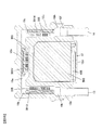
- インバータ回路の上下アームを構成する複数のパワー半導体素子と、
多面体形状を有し、前記複数のパワー半導体素子を封止する第1封止部材と、
前記複数のパワー半導体素子のいずれかと接続され、前記第1封止部材から突出する正極側端子と、
前記複数のパワー半導体素子のいずれかと接続され、前記第1封止部材から突出する負極側端子と、
前記正極側端子の少なくとも一部及び前記負極側端子の少なくとも一部を封止する第2封止部材と、
前記第1封止部材で封止された前記パワー半導体素子を収納するケースと、を備え、
前記正極側端子及び前記負極側端子は、前記第1封止部材から突出する部分が前記第1封止部材の一つの面に沿って一列に並べられ、
さらに、前記正極側端子及び前記負極側端子は、前記第2封止部材から積層状態で突出しておりかつ前記ケースの外に延出していることを特徴とするパワー半導体装置。 - 請求項1に記載のパワー半導体装置において、
前記正極側端子及び前記負極側端子の各層を流れる電流により互いに相殺し合う方向の磁束を発生することを特徴とするパワー半導体装置。 - 請求項1または2に記載のパワー半導体装置において、
前記ケースは、電気伝導性を有する部材で形成され、
前記上下アームの直列回路を流れる電流により前記ケースに渦電流が誘起されることを特徴とするパワー半導体装置。 - 請求項1乃至3のいずれか一項に記載のパワー半導体装置において、
前記ケースは、その外側に放熱用のフィンを有する放熱面が形成され、
前記ケースの内側に前記放熱面に対向するようにして、前記第1封止部材で封止された前記複数のパワー半導体素子が配置されることを特徴とするパワー半導体装置。 - 請求項1乃至4のいずれか一項に記載のパワー半導体装置において、
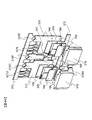
前記パワー半導体素子の駆動信号を伝達する信号接続端子と、
前記信号接続端子と金属接合により接続される信号配線と、をさらに備え、
前記正極側端子は、前記上下アームの直列回路に直流電力を供給するための直流正極接続端子と、前記直流正極接続端子と金属接合により接続される直流正極配線と、を含み、
前記負極側端子は、前記上下アームの直列回路に直流電力を供給するための直流負極接続端子と、前記直流負極接続端子と金属接合により接続される直流負極配線と、を含み、
前記第2封止部材は、前記信号接続端子と前記信号配線との接続部、前記直流正極接続端子と前記直流正極配線との接続部、及び前記直流負極接続端子と前記直流負極配線との接続部を封止することを特徴とするパワー半導体装置。 - 請求項5に記載のパワー半導体装置において、
前記信号接続端子、前記直流正極接続端子及び前記直流負極接続端子は、前記第1封止部材から同一方向にそれぞれ突出し、
前記信号接続端子、前記直流正極接続端子及び前記直流負極接続端子のそれぞれの端部は、同一方向にそれぞれ折り曲げられ、
前記信号接続端子、前記直流正極接続端子及び前記直流負極接続端子の折り曲げられた端部が、それぞれ前記信号配線、前記直流正極配線または前記直流負極配線と金属接続されることを特徴とするパワー半導体装置。 - 請求項5または6に記載のパワー半導体装置において、
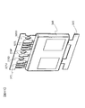
前記信号接続端子、前記直流正極接続端子及び前記直流負極接続端子は、前記第1封止部材から突出する部分が一列に配置されることを特徴とするパワー半導体装置。 - 請求項1乃至7のいずれか一項に記載のパワー半導体装置において、
前記第1封止部材から突出しており、前記上下アームの直列回路により直流電力から変換された交流電力を出力するための交流接続端子と、
前記交流接続端子と金属接合により接続される交流配線と、をさらに備え、
前記第2封止部材は、前記交流接続端子と前記交流配線との接続部をさらに封止することを特徴とするパワー半導体装置。 - 請求項5乃至7のいずれか一項に記載のパワー半導体装置において、
前記ケースは、一つの開口面を有しており、
前記直流正極接続端子と前記直流正極配線との接続部、及び前記直流負極接続端子と前記直流負極配線との接続部は、前記開口面よりも前記ケースの内側に配置され、
前記直流正極配線及び前記直流負極配線は、前記開口面から前記ケースの外に延出することを特徴とするパワー半導体装置。 - 請求項5乃至7、9のいずれか一項に記載のパワー半導体装置において、
前記直流正極配線及び前記直流負極配線を支持する支持部材をさらに備え、
前記支持部材は、前記ケースに固定されることを特徴とするパワー半導体装置。 - 請求項1乃至10のいずれか一項に記載のパワー半導体装置において、
前記第2封止部材は、前記ケースの内側と前記第1封止部材との間の空間に充填されることを特徴とするパワー半導体装置。
Priority Applications (13)
| Application Number | Priority Date | Filing Date | Title |
|---|---|---|---|
| JP2010140723A JP5380376B2 (ja) | 2010-06-21 | 2010-06-21 | パワー半導体装置 |
| EP11169980.7A EP2416483B1 (en) | 2010-06-21 | 2011-06-15 | Power semiconductor device and power conversion device |
| EP19175045.4A EP3562020B1 (en) | 2010-06-21 | 2011-06-15 | Power semiconductor device and power conversion device |
| US13/163,950 US9179581B2 (en) | 2010-06-21 | 2011-06-20 | Power semiconductor device and power conversion device |
| CN201110176325.1A CN102332831B (zh) | 2010-06-21 | 2011-06-21 | 功率半导体装置及使用其的电力转换装置 |
| JP2013205250A JP5744999B2 (ja) | 2010-06-21 | 2013-09-30 | パワー半導体装置、パワー半導体装置の製造方法 |
| JP2015089935A JP5973026B2 (ja) | 2010-06-21 | 2015-04-27 | パワー半導体装置 |
| US14/856,819 US10034401B2 (en) | 2010-06-21 | 2015-09-17 | Power semiconductor device and power conversion device |
| JP2016138115A JP6663810B2 (ja) | 2010-06-21 | 2016-07-13 | パワー半導体装置及びそれを用いた電力変換装置 |
| US16/017,827 US10512181B2 (en) | 2010-06-21 | 2018-06-25 | Power semiconductor device and power conversion device |
| JP2019011798A JP6818785B6 (ja) | 2010-06-21 | 2019-01-28 | パワー半導体装置及びそれを用いた電力変換装置 |
| US16/671,872 US11432419B2 (en) | 2010-06-21 | 2019-11-01 | Power semiconductor device and power conversion device |
| JP2020211955A JP7012813B2 (ja) | 2010-06-21 | 2020-12-22 | パワー半導体装置及びそれを用いた電力変換装置 |
Applications Claiming Priority (1)
| Application Number | Priority Date | Filing Date | Title |
|---|---|---|---|
| JP2010140723A JP5380376B2 (ja) | 2010-06-21 | 2010-06-21 | パワー半導体装置 |
Related Child Applications (1)
| Application Number | Title | Priority Date | Filing Date |
|---|---|---|---|
| JP2013205250A Division JP5744999B2 (ja) | 2010-06-21 | 2013-09-30 | パワー半導体装置、パワー半導体装置の製造方法 |
Publications (3)
| Publication Number | Publication Date |
|---|---|
| JP2012005322A JP2012005322A (ja) | 2012-01-05 |
| JP2012005322A5 JP2012005322A5 (ja) | 2012-11-01 |
| JP5380376B2 true JP5380376B2 (ja) | 2014-01-08 |
Family
ID=44720535
Family Applications (6)
| Application Number | Title | Priority Date | Filing Date |
|---|---|---|---|
| JP2010140723A Active JP5380376B2 (ja) | 2010-06-21 | 2010-06-21 | パワー半導体装置 |
| JP2013205250A Active JP5744999B2 (ja) | 2010-06-21 | 2013-09-30 | パワー半導体装置、パワー半導体装置の製造方法 |
| JP2015089935A Active JP5973026B2 (ja) | 2010-06-21 | 2015-04-27 | パワー半導体装置 |
| JP2016138115A Active JP6663810B2 (ja) | 2010-06-21 | 2016-07-13 | パワー半導体装置及びそれを用いた電力変換装置 |
| JP2019011798A Active JP6818785B6 (ja) | 2010-06-21 | 2019-01-28 | パワー半導体装置及びそれを用いた電力変換装置 |
| JP2020211955A Active JP7012813B2 (ja) | 2010-06-21 | 2020-12-22 | パワー半導体装置及びそれを用いた電力変換装置 |
Family Applications After (5)
| Application Number | Title | Priority Date | Filing Date |
|---|---|---|---|
| JP2013205250A Active JP5744999B2 (ja) | 2010-06-21 | 2013-09-30 | パワー半導体装置、パワー半導体装置の製造方法 |
| JP2015089935A Active JP5973026B2 (ja) | 2010-06-21 | 2015-04-27 | パワー半導体装置 |
| JP2016138115A Active JP6663810B2 (ja) | 2010-06-21 | 2016-07-13 | パワー半導体装置及びそれを用いた電力変換装置 |
| JP2019011798A Active JP6818785B6 (ja) | 2010-06-21 | 2019-01-28 | パワー半導体装置及びそれを用いた電力変換装置 |
| JP2020211955A Active JP7012813B2 (ja) | 2010-06-21 | 2020-12-22 | パワー半導体装置及びそれを用いた電力変換装置 |
Country Status (4)
| Country | Link |
|---|---|
| US (4) | US9179581B2 (ja) |
| EP (2) | EP2416483B1 (ja) |
| JP (6) | JP5380376B2 (ja) |
| CN (1) | CN102332831B (ja) |
Cited By (1)
| Publication number | Priority date | Publication date | Assignee | Title |
|---|---|---|---|---|
| JP2015156800A (ja) * | 2010-06-21 | 2015-08-27 | 日立オートモティブシステムズ株式会社 | パワー半導体装置及びそれを用いた電力変換装置 |
Families Citing this family (93)
| Publication number | Priority date | Publication date | Assignee | Title |
|---|---|---|---|---|
| JP4848187B2 (ja) * | 2006-01-17 | 2011-12-28 | 日立オートモティブシステムズ株式会社 | 電力変換装置 |
| JP4657329B2 (ja) * | 2008-07-29 | 2011-03-23 | 日立オートモティブシステムズ株式会社 | 電力変換装置および電動車両 |
| US10321585B2 (en) | 2008-07-29 | 2019-06-11 | Hitachi, Ltd. | Power conversion apparatus and electric vehicle |
| JP5557585B2 (ja) * | 2010-04-26 | 2014-07-23 | 日立オートモティブシステムズ株式会社 | パワーモジュール |
| JP5581131B2 (ja) * | 2010-06-30 | 2014-08-27 | 日立オートモティブシステムズ株式会社 | パワーモジュール及びそれを用いた電力変換装置 |
| JP5858934B2 (ja) * | 2011-02-02 | 2016-02-10 | ローム株式会社 | 半導体パワーデバイスおよびその製造方法 |
| JP5506740B2 (ja) | 2011-05-31 | 2014-05-28 | 日立オートモティブシステムズ株式会社 | 電力変換装置 |
| JP5502805B2 (ja) | 2011-06-08 | 2014-05-28 | 日立オートモティブシステムズ株式会社 | パワーモジュールおよびそれを用いた電力変換装置 |
| JP5520889B2 (ja) | 2011-06-24 | 2014-06-11 | 日立オートモティブシステムズ株式会社 | パワー半導体モジュール及びそれを用いた電力変換装置 |
| JP5651552B2 (ja) * | 2011-07-22 | 2015-01-14 | 日立オートモティブシステムズ株式会社 | 電力変換装置 |
| JP5338932B2 (ja) * | 2011-07-26 | 2013-11-13 | 株式会社デンソー | 電力変換装置 |
| JP5508357B2 (ja) | 2011-07-29 | 2014-05-28 | 日立オートモティブシステムズ株式会社 | 電力変換装置 |
| JP5567530B2 (ja) | 2011-08-19 | 2014-08-06 | 日立オートモティブシステムズ株式会社 | 摩擦攪拌接合構造およびパワー半導体装置 |
| US9048721B2 (en) * | 2011-09-27 | 2015-06-02 | Keihin Corporation | Semiconductor device |
| CN103023279B (zh) * | 2011-09-27 | 2015-05-13 | 株式会社京浜 | 半导体控制装置 |
| JP5813137B2 (ja) * | 2011-12-26 | 2015-11-17 | 三菱電機株式会社 | 電力用半導体装置及びその製造方法 |
| WO2013140502A1 (ja) * | 2012-03-19 | 2013-09-26 | 三菱電機株式会社 | 電力変換装置 |
| CN104170085B (zh) * | 2012-03-28 | 2017-05-10 | 富士电机株式会社 | 半导体装置 |
| JP5838918B2 (ja) * | 2012-06-13 | 2016-01-06 | 株式会社デンソー | 電力変換装置 |
| JP5747869B2 (ja) * | 2012-06-18 | 2015-07-15 | 株式会社デンソー | 電力変換装置 |
| JP5699995B2 (ja) * | 2012-07-02 | 2015-04-15 | 株式会社デンソー | 電力変換装置 |
| JP2014027797A (ja) | 2012-07-27 | 2014-02-06 | Yazaki Corp | 電気接続箱 |
| JP5941787B2 (ja) * | 2012-08-09 | 2016-06-29 | 日立オートモティブシステムズ株式会社 | パワーモジュールおよびパワーモジュールの製造方法 |
| JP5879233B2 (ja) * | 2012-08-31 | 2016-03-08 | 日立オートモティブシステムズ株式会社 | パワー半導体モジュール |
| JP5874838B2 (ja) * | 2012-09-19 | 2016-03-02 | 日産自動車株式会社 | 電動車両用強電ユニットの搭載構造 |
| JP5851372B2 (ja) * | 2012-09-28 | 2016-02-03 | 日立オートモティブシステムズ株式会社 | 電力変換装置 |
| JP2014074678A (ja) * | 2012-10-05 | 2014-04-24 | Tokai Rika Co Ltd | 電流検出装置 |
| KR101890752B1 (ko) | 2012-11-01 | 2018-08-22 | 삼성전자 주식회사 | 균일한 병렬 스위치 특성을 갖는 파워모듈용 기판 및 이를 포함하는 파워모듈 |
| ITMO20120321A1 (it) * | 2012-12-21 | 2014-06-22 | Meta System Spa | Procedimento per la realizzazione e l'assemblaggio di schede elettroniche e dispositivo elettronico cosi' ottenibile |
| US9730365B2 (en) * | 2012-12-30 | 2017-08-08 | General Electric Company | Heat sink apparatus and method for power semiconductor device module |
| JP5701412B2 (ja) * | 2013-02-21 | 2015-04-15 | 株式会社デンソー | 電力変換装置 |
| JP5932704B2 (ja) * | 2013-04-04 | 2016-06-08 | 株式会社日本自動車部品総合研究所 | 電力変換装置 |
| JP6364704B2 (ja) * | 2013-04-30 | 2018-08-01 | 株式会社明電舎 | 車載用電力変換装置 |
| US9992915B2 (en) * | 2013-10-07 | 2018-06-05 | Hitachi Automotive Systems, Ltd. | Power conversion device |
| JP5505915B1 (ja) * | 2013-10-30 | 2014-05-28 | 太陽誘電株式会社 | 通信モジュール |
| US9160825B2 (en) * | 2013-10-30 | 2015-10-13 | Taiyo Yuden Co., Ltd. | Communication module |
| JP6102691B2 (ja) * | 2013-11-15 | 2017-03-29 | 株式会社デンソー | 電力変換装置 |
| US20150138734A1 (en) * | 2013-11-18 | 2015-05-21 | Magna Electronics Inc. | 360 degree direct cooled power module |
| JP6112003B2 (ja) * | 2013-12-18 | 2017-04-12 | トヨタ自動車株式会社 | 冷却機能付き電子装置 |
| JP5991345B2 (ja) * | 2013-12-26 | 2016-09-14 | 株式会社デンソー | 電力変換装置 |
| US10080313B2 (en) * | 2014-01-27 | 2018-09-18 | Hitachi, Ltd. | Power module and method for manufacturing the same |
| KR20150111422A (ko) * | 2014-03-21 | 2015-10-06 | 엘에스산전 주식회사 | 자동차용 전장 부품 케이스 |
| JP6256145B2 (ja) * | 2014-03-26 | 2018-01-10 | 株式会社デンソー | 半導体装置及びその製造方法 |
| US10564193B2 (en) * | 2014-04-30 | 2020-02-18 | Onbalance Technologies Inc. | Energy monitoring and analysis system |
| JP6245075B2 (ja) * | 2014-05-28 | 2017-12-13 | アイシン・エィ・ダブリュ株式会社 | 車両用駆動装置 |
| JP6354392B2 (ja) * | 2014-07-03 | 2018-07-11 | 株式会社デンソー | 半導体装置 |
| US9829516B1 (en) * | 2014-09-23 | 2017-11-28 | Amazon Technologies, Inc. | Non-intrusive transient power detection system |
| EP3217535B1 (en) * | 2014-11-04 | 2021-04-28 | Mitsubishi Electric Corporation | Motor drive device and air conditioner |
| JP6312852B2 (ja) * | 2014-11-04 | 2018-04-18 | 三菱電機株式会社 | 電動機駆動装置および空気調和機 |
| CN107112898B (zh) | 2014-11-18 | 2019-06-21 | 通用电气全球采购有限责任公司 | 母线和功率电子装置及制造引线端连接器的方法 |
| JP6382097B2 (ja) * | 2014-12-24 | 2018-08-29 | 株式会社 日立パワーデバイス | 半導体パワーモジュールおよびそれを用いた電力変換装置 |
| JP6415605B2 (ja) * | 2015-01-19 | 2018-10-31 | 三菱電機株式会社 | コントローラ |
| JPWO2016181516A1 (ja) * | 2015-05-13 | 2017-08-03 | 三菱電機株式会社 | 半導体モジュール |
| DE102015209279A1 (de) * | 2015-05-21 | 2016-11-24 | Robert Bosch Gmbh | Elektrische Kontaktanordnung |
| US10312801B2 (en) * | 2015-07-09 | 2019-06-04 | Ce+T Power Luxembourg S.A. | High power density inverter (II) |
| US9584061B1 (en) * | 2015-09-17 | 2017-02-28 | Toyota Motor Engineering & Manufacturing North America, Inc. | Electric drive systems including smoothing capacitor cooling devices and systems |
| FR3043880B1 (fr) * | 2015-11-13 | 2017-12-29 | Valeo Systemes De Controle Moteur | Boitier pour un equipement electrique |
| KR101629397B1 (ko) * | 2015-12-03 | 2016-06-13 | 연세대학교 산학협력단 | 비대칭 모듈러 멀티레벨 컨버터 제어 장치 및 방법 |
| DE112016005528T5 (de) * | 2015-12-04 | 2018-08-30 | Rohm Co., Ltd. | Leistungsmodulvorrichtung, Kühlstruktur und elektrisches Fahrzeug oder elektrisches Hybridfahrzeug |
| JP6544222B2 (ja) * | 2015-12-11 | 2019-07-17 | 住友電気工業株式会社 | 半導体モジュール及び半導体モジュールユニット |
| USD811437S1 (en) * | 2016-03-30 | 2018-02-27 | Siemens Aktiengesellschaft | Motor controller |
| JP6209644B1 (ja) * | 2016-04-27 | 2017-10-04 | カルソニックカンセイ株式会社 | 半導体装置の冷却装置 |
| JP6575930B2 (ja) * | 2016-06-02 | 2019-09-18 | 株式会社オートネットワーク技術研究所 | 基板ユニット |
| WO2017221456A1 (ja) * | 2016-06-21 | 2017-12-28 | 三菱電機株式会社 | 電力変換装置 |
| CN107851636B (zh) * | 2016-07-15 | 2020-08-14 | 新电元工业株式会社 | 半导体模块 |
| DE102016120778B4 (de) | 2016-10-31 | 2024-01-25 | Infineon Technologies Ag | Baugruppe mit vertikal beabstandeten, teilweise verkapselten Kontaktstrukturen |
| JP6702155B2 (ja) * | 2016-11-22 | 2020-05-27 | トヨタ自動車株式会社 | インバータの車載構造 |
| JP6594916B2 (ja) * | 2017-01-12 | 2019-10-23 | 日立オートモティブシステムズ株式会社 | 電流検出装置 |
| CN110168907B (zh) * | 2017-01-13 | 2021-07-23 | 日立汽车系统株式会社 | 电力转换装置 |
| JP6750514B2 (ja) | 2017-01-18 | 2020-09-02 | 株式会社デンソー | 半導体装置 |
| JP2019033628A (ja) * | 2017-08-09 | 2019-02-28 | 株式会社デンソー | 電力変換装置 |
| JP6640165B2 (ja) * | 2017-09-29 | 2020-02-05 | 三菱電機株式会社 | 電力変換装置 |
| CN110164858B (zh) * | 2018-02-16 | 2023-05-05 | 株式会社电装 | 半导体器件 |
| KR102532313B1 (ko) * | 2018-03-07 | 2023-05-15 | 현대자동차주식회사 | 차량용 하이브리드 전력제어장치 |
| WO2020049891A1 (ja) * | 2018-09-05 | 2020-03-12 | 日立オートモティブシステムズ株式会社 | パワー半導体装置 |
| KR102554431B1 (ko) * | 2018-09-05 | 2023-07-13 | 삼성전자주식회사 | 반도체 장치 및 반도체 장치 제조 방법 |
| FR3091138B1 (fr) * | 2018-12-21 | 2022-07-22 | Valeo Siemens Eautomotive France Sas | Ensemble électrique comprenant des moyens de blindage électromagnétique intégrés |
| CN113228482B (zh) * | 2018-12-26 | 2024-03-08 | 松下知识产权经营株式会社 | 电力转换装置 |
| EP3687059A1 (de) * | 2019-01-22 | 2020-07-29 | Siemens Aktiengesellschaft | Betreiben von schaltelementen eines mehrpegelenergiewandlers |
| JP7120083B2 (ja) * | 2019-03-06 | 2022-08-17 | 株式会社デンソー | 半導体装置 |
| JP7003964B2 (ja) * | 2019-04-05 | 2022-01-21 | 株式会社デンソー | 電力変換装置 |
| JP7180540B2 (ja) * | 2019-05-28 | 2022-11-30 | 株式会社デンソー | 電力変換ユニット |
| US10667413B1 (en) * | 2019-07-01 | 2020-05-26 | Sumitomo Wiring Systems, Ltd. | Power distribution box assembly with terminal tower |
| DE102019214789A1 (de) | 2019-09-26 | 2021-04-01 | Zf Friedrichshafen Ag | Steuergerät zum Betreiben eines Elektroantriebs für ein Fahrzeug und Verfahren zum Herstellen eines deratigen Steuergeräts |
| DE102019216679A1 (de) * | 2019-10-29 | 2021-04-29 | Zf Friedrichshafen Ag | Elektronikmodul für einen Elektroantrieb eines Fahrzeugs mit gleichlangen Strompfaden für einen Highside-Schalter und einen Lowside-Schalter |
| WO2021176934A1 (ja) * | 2020-03-05 | 2021-09-10 | 富士電機株式会社 | 電力変換装置 |
| US20210367526A1 (en) * | 2020-05-22 | 2021-11-25 | Marel Power Solutions, Inc. | Packaged power module |
| EP3951851A1 (de) * | 2020-08-05 | 2022-02-09 | Siemens Aktiengesellschaft | Leistungshalbleitermodulsystem und herstellungsverfahren für ein leistungshalbleitermodulsystem |
| CN112706631B (zh) * | 2020-12-21 | 2022-04-26 | 中车永济电机有限公司 | 一种高功率密度水冷双向充电机装置 |
| GB2602338B (en) * | 2020-12-23 | 2023-03-15 | Yasa Ltd | A Method and Apparatus for Cooling One or More Power Devices |
| CN117378291A (zh) | 2021-05-27 | 2024-01-09 | 法雷奥新能源汽车德国有限责任公司 | 冷却结构、包括这种冷却结构的功率模块、包括这种功率模块的诸如逆变器的电功率转换器 |
| WO2023113824A1 (en) * | 2021-12-17 | 2023-06-22 | Vishay SIliconix, LLC | Semiconductor device and method of forming components for semiconductor device |
| CN115038312A (zh) * | 2022-06-24 | 2022-09-09 | 中国第一汽车股份有限公司 | 电机控制器的功率封装模块 |
Family Cites Families (40)
| Publication number | Priority date | Publication date | Assignee | Title |
|---|---|---|---|---|
| US5202578A (en) * | 1989-09-11 | 1993-04-13 | Kabushiki Kaisha Toshiba | Module-type semiconductor device of high power capacity |
| JP3129020B2 (ja) | 1992-04-09 | 2001-01-29 | 富士電機株式会社 | 半導体装置 |
| JP2912526B2 (ja) * | 1993-07-05 | 1999-06-28 | 三菱電機株式会社 | 半導体パワーモジュールおよび複合基板 |
| EP0706221B8 (en) * | 1994-10-07 | 2008-09-03 | Hitachi, Ltd. | Semiconductor device comprising a plurality of semiconductor elements |
| JPH1010508A (ja) * | 1996-06-25 | 1998-01-16 | Toshiba Corp | 液晶セルの組立装置 |
| JP3674333B2 (ja) * | 1998-09-11 | 2005-07-20 | 株式会社日立製作所 | パワー半導体モジュール並びにそれを用いた電動機駆動システム |
| JP3642012B2 (ja) * | 2000-07-21 | 2005-04-27 | 株式会社日立製作所 | 半導体装置,電力変換装置及び自動車 |
| JP2002315357A (ja) * | 2001-04-16 | 2002-10-25 | Hitachi Ltd | インバータ装置 |
| JP3910383B2 (ja) | 2001-07-17 | 2007-04-25 | 株式会社日立製作所 | パワーモジュールおよびインバータ |
| JP3740117B2 (ja) * | 2002-11-13 | 2006-02-01 | 三菱電機株式会社 | 電力用半導体装置 |
| JP2004208411A (ja) | 2002-12-25 | 2004-07-22 | Denso Corp | ハーフブリッジ回路用半導体モジュール |
| JP2004265931A (ja) * | 2003-02-14 | 2004-09-24 | Hitachi Ltd | 半導体素子駆動用集積回路及び電力変換装置 |
| US6933593B2 (en) * | 2003-08-14 | 2005-08-23 | International Rectifier Corporation | Power module having a heat sink |
| EP2216892B1 (en) * | 2003-08-21 | 2012-01-18 | Denso Corporation | Mounting structure of a semiconductor device |
| US7358442B2 (en) * | 2003-09-30 | 2008-04-15 | Rockwell Automation Technologies, Inc. | Bus structure for power switching circuits |
| US7301755B2 (en) * | 2003-12-17 | 2007-11-27 | Siemens Vdo Automotive Corporation | Architecture for power modules such as power inverters |
| JP4566678B2 (ja) * | 2004-10-04 | 2010-10-20 | 日立オートモティブシステムズ株式会社 | パワーモジュール |
| JP4547231B2 (ja) * | 2004-10-22 | 2010-09-22 | 日立オートモティブシステムズ株式会社 | 電力変換装置 |
| JP2006120970A (ja) * | 2004-10-25 | 2006-05-11 | Toyota Motor Corp | 半導体モジュールとその製造方法 |
| JP4569766B2 (ja) * | 2005-05-31 | 2010-10-27 | トヨタ自動車株式会社 | 半導体装置 |
| JP4581885B2 (ja) * | 2005-07-22 | 2010-11-17 | 株式会社デンソー | 半導体装置 |
| JP4979909B2 (ja) | 2005-08-19 | 2012-07-18 | 株式会社日立製作所 | 電力変換装置 |
| JP4603956B2 (ja) * | 2005-08-26 | 2010-12-22 | 日立オートモティブシステムズ株式会社 | 電力変換装置 |
| EP2202792B1 (en) * | 2006-06-09 | 2016-11-23 | Honda Motor Co., Ltd. | Semiconductor device |
| JP2008118067A (ja) * | 2006-11-08 | 2008-05-22 | Hitachi Ltd | パワーモジュール及びモータ一体型コントロール装置 |
| JP4909712B2 (ja) * | 2006-11-13 | 2012-04-04 | 日立オートモティブシステムズ株式会社 | 電力変換装置 |
| JP2008227131A (ja) | 2007-03-13 | 2008-09-25 | Renesas Technology Corp | 半導体装置及びその製造方法 |
| JP5227532B2 (ja) * | 2007-04-02 | 2013-07-03 | 日立オートモティブシステムズ株式会社 | インバータ回路用の半導体モジュール |
| JP4452952B2 (ja) * | 2007-06-20 | 2010-04-21 | 日立オートモティブシステムズ株式会社 | 電力変換装置 |
| JP4567029B2 (ja) * | 2007-06-22 | 2010-10-20 | 日立オートモティブシステムズ株式会社 | 電力変換装置 |
| JP4452953B2 (ja) * | 2007-08-09 | 2010-04-21 | 日立オートモティブシステムズ株式会社 | 電力変換装置 |
| JP4580997B2 (ja) | 2008-03-11 | 2010-11-17 | 日立オートモティブシステムズ株式会社 | 電力変換装置 |
| JP5067267B2 (ja) * | 2008-06-05 | 2012-11-07 | 三菱電機株式会社 | 樹脂封止型半導体装置とその製造方法 |
| JP4666185B2 (ja) * | 2008-06-26 | 2011-04-06 | 三菱電機株式会社 | 半導体装置 |
| JP4988665B2 (ja) | 2008-08-06 | 2012-08-01 | 日立オートモティブシステムズ株式会社 | 半導体装置および半導体装置を用いた電力変換装置 |
| JP5098951B2 (ja) * | 2008-10-22 | 2012-12-12 | 富士電機株式会社 | 半導体装置 |
| JP5002568B2 (ja) | 2008-10-29 | 2012-08-15 | 日立オートモティブシステムズ株式会社 | 電力変換装置 |
| JP5557441B2 (ja) * | 2008-10-31 | 2014-07-23 | 日立オートモティブシステムズ株式会社 | 電力変換装置および電動車両 |
| JP2010140723A (ja) | 2008-12-10 | 2010-06-24 | Autonetworks Technologies Ltd | 車輌用スイッチシステム |
| JP5380376B2 (ja) * | 2010-06-21 | 2014-01-08 | 日立オートモティブシステムズ株式会社 | パワー半導体装置 |
-
2010
- 2010-06-21 JP JP2010140723A patent/JP5380376B2/ja active Active
-
2011
- 2011-06-15 EP EP11169980.7A patent/EP2416483B1/en active Active
- 2011-06-15 EP EP19175045.4A patent/EP3562020B1/en active Active
- 2011-06-20 US US13/163,950 patent/US9179581B2/en active Active
- 2011-06-21 CN CN201110176325.1A patent/CN102332831B/zh active Active
-
2013
- 2013-09-30 JP JP2013205250A patent/JP5744999B2/ja active Active
-
2015
- 2015-04-27 JP JP2015089935A patent/JP5973026B2/ja active Active
- 2015-09-17 US US14/856,819 patent/US10034401B2/en active Active
-
2016
- 2016-07-13 JP JP2016138115A patent/JP6663810B2/ja active Active
-
2018
- 2018-06-25 US US16/017,827 patent/US10512181B2/en active Active
-
2019
- 2019-01-28 JP JP2019011798A patent/JP6818785B6/ja active Active
- 2019-11-01 US US16/671,872 patent/US11432419B2/en active Active
-
2020
- 2020-12-22 JP JP2020211955A patent/JP7012813B2/ja active Active
Cited By (2)
| Publication number | Priority date | Publication date | Assignee | Title |
|---|---|---|---|---|
| JP2015156800A (ja) * | 2010-06-21 | 2015-08-27 | 日立オートモティブシステムズ株式会社 | パワー半導体装置及びそれを用いた電力変換装置 |
| JP2019071784A (ja) * | 2010-06-21 | 2019-05-09 | 日立オートモティブシステムズ株式会社 | パワー半導体装置及びそれを用いた電力変換装置 |
Also Published As
| Publication number | Publication date |
|---|---|
| EP2416483B1 (en) | 2019-08-07 |
| JP6663810B2 (ja) | 2020-03-13 |
| EP3562020B1 (en) | 2022-04-20 |
| US20110310585A1 (en) | 2011-12-22 |
| JP6818785B6 (ja) | 2021-03-17 |
| US20180303001A1 (en) | 2018-10-18 |
| CN102332831B (zh) | 2014-08-20 |
| JP2014027877A (ja) | 2014-02-06 |
| JP2016182037A (ja) | 2016-10-13 |
| EP3562020A1 (en) | 2019-10-30 |
| JP6818785B2 (ja) | 2021-01-20 |
| JP2021052587A (ja) | 2021-04-01 |
| US10512181B2 (en) | 2019-12-17 |
| JP5973026B2 (ja) | 2016-08-17 |
| JP5744999B2 (ja) | 2015-07-08 |
| CN102332831A (zh) | 2012-01-25 |
| EP2416483A2 (en) | 2012-02-08 |
| US20160007492A1 (en) | 2016-01-07 |
| US9179581B2 (en) | 2015-11-03 |
| JP2012005322A (ja) | 2012-01-05 |
| US11432419B2 (en) | 2022-08-30 |
| US20200068735A1 (en) | 2020-02-27 |
| JP7012813B2 (ja) | 2022-01-28 |
| US10034401B2 (en) | 2018-07-24 |
| JP2015156800A (ja) | 2015-08-27 |
| JP2019071784A (ja) | 2019-05-09 |
| EP2416483A3 (en) | 2017-06-28 |
Similar Documents
| Publication | Publication Date | Title |
|---|---|---|
| JP7012813B2 (ja) | パワー半導体装置及びそれを用いた電力変換装置 | |
| JP5563383B2 (ja) | 電力変換装置 | |
| JP5592496B2 (ja) | 電力変換装置 | |
| JP5422466B2 (ja) | 電力変換装置 | |
| JP5455888B2 (ja) | 車両用電力変換装置 | |
| JP5422468B2 (ja) | 電力変換装置 | |
| JP5588895B2 (ja) | パワー半導体モジュール,パワー半導体モジュールの製造方法及び電力変換装置 | |
| JP5508357B2 (ja) | 電力変換装置 | |
| JP5651552B2 (ja) | 電力変換装置 | |
| WO2012165341A1 (ja) | 電力変換装置 | |
| JP2013115903A (ja) | 機電一体型の電動駆動装置 | |
| JP2014113053A (ja) | 電力変換装置 | |
| JP2013138609A (ja) | 半導体モジュール及びこれを備えた電力変換装置 | |
| JP5857092B2 (ja) | 電力変換装置 |
Legal Events
| Date | Code | Title | Description |
|---|---|---|---|
| A521 | Request for written amendment filed |
Free format text: JAPANESE INTERMEDIATE CODE: A523 Effective date: 20120912 |
|
| A621 | Written request for application examination |
Free format text: JAPANESE INTERMEDIATE CODE: A621 Effective date: 20120912 |
|
| A977 | Report on retrieval |
Free format text: JAPANESE INTERMEDIATE CODE: A971007 Effective date: 20130830 |
|
| TRDD | Decision of grant or rejection written | ||
| A01 | Written decision to grant a patent or to grant a registration (utility model) |
Free format text: JAPANESE INTERMEDIATE CODE: A01 Effective date: 20130903 |
|
| A61 | First payment of annual fees (during grant procedure) |
Free format text: JAPANESE INTERMEDIATE CODE: A61 Effective date: 20130930 |
|
| R150 | Certificate of patent or registration of utility model |
Ref document number: 5380376 Country of ref document: JP Free format text: JAPANESE INTERMEDIATE CODE: R150 Free format text: JAPANESE INTERMEDIATE CODE: R150 |
|
| S533 | Written request for registration of change of name |
Free format text: JAPANESE INTERMEDIATE CODE: R313533 |
|
| R350 | Written notification of registration of transfer |
Free format text: JAPANESE INTERMEDIATE CODE: R350 |