EP1535343B1 - Transistor a effet de champ a grille isolee presentant des barrieres de schottky passivees vers le canal - Google Patents
Transistor a effet de champ a grille isolee presentant des barrieres de schottky passivees vers le canal Download PDFInfo
- Publication number
- EP1535343B1 EP1535343B1 EP03785158.1A EP03785158A EP1535343B1 EP 1535343 B1 EP1535343 B1 EP 1535343B1 EP 03785158 A EP03785158 A EP 03785158A EP 1535343 B1 EP1535343 B1 EP 1535343B1
- Authority
- EP
- European Patent Office
- Prior art keywords
- channel
- semiconductor
- transistor
- metal
- source
- Prior art date
- Legal status (The legal status is an assumption and is not a legal conclusion. Google has not performed a legal analysis and makes no representation as to the accuracy of the status listed.)
- Expired - Lifetime
Links
- 230000004888 barrier function Effects 0.000 title description 45
- 230000005669 field effect Effects 0.000 title description 9
- 239000010410 layer Substances 0.000 claims description 166
- 239000004065 semiconductor Substances 0.000 claims description 145
- 229910052751 metal Inorganic materials 0.000 claims description 85
- 239000002184 metal Substances 0.000 claims description 85
- 239000000463 material Substances 0.000 claims description 52
- 229910052710 silicon Inorganic materials 0.000 claims description 35
- XUIMIQQOPSSXEZ-UHFFFAOYSA-N Silicon Chemical compound [Si] XUIMIQQOPSSXEZ-UHFFFAOYSA-N 0.000 claims description 33
- 239000010703 silicon Substances 0.000 claims description 33
- 229910052782 aluminium Inorganic materials 0.000 claims description 24
- XAGFODPZIPBFFR-UHFFFAOYSA-N aluminium Chemical compound [Al] XAGFODPZIPBFFR-UHFFFAOYSA-N 0.000 claims description 24
- 238000000926 separation method Methods 0.000 claims description 11
- 230000000694 effects Effects 0.000 claims description 10
- 239000002356 single layer Substances 0.000 claims description 8
- KRHYYFGTRYWZRS-UHFFFAOYSA-M Fluoride anion Chemical compound [F-] KRHYYFGTRYWZRS-UHFFFAOYSA-M 0.000 claims description 5
- 229910052732 germanium Inorganic materials 0.000 claims description 5
- 150000004678 hydrides Chemical class 0.000 claims description 5
- 150000004767 nitrides Chemical class 0.000 claims description 5
- 239000000126 substance Substances 0.000 claims description 5
- 229910000577 Silicon-germanium Inorganic materials 0.000 claims description 4
- 229910045601 alloy Inorganic materials 0.000 claims description 4
- 239000000956 alloy Substances 0.000 claims description 4
- GNPVGFCGXDBREM-UHFFFAOYSA-N germanium atom Chemical compound [Ge] GNPVGFCGXDBREM-UHFFFAOYSA-N 0.000 claims description 3
- 229910003465 moissanite Inorganic materials 0.000 claims description 3
- 229910010271 silicon carbide Inorganic materials 0.000 claims description 3
- 229910003811 SiGeC Inorganic materials 0.000 claims description 2
- HYIMSNHJOBLJNT-UHFFFAOYSA-N nifedipine Chemical compound COC(=O)C1=C(C)NC(C)=C(C(=O)OC)C1C1=CC=CC=C1[N+]([O-])=O HYIMSNHJOBLJNT-UHFFFAOYSA-N 0.000 claims description 2
- 239000003870 refractory metal Substances 0.000 claims description 2
- 239000000758 substrate Substances 0.000 description 42
- 238000002161 passivation Methods 0.000 description 24
- 239000012212 insulator Substances 0.000 description 22
- 238000000034 method Methods 0.000 description 21
- 150000002739 metals Chemical class 0.000 description 13
- 238000004519 manufacturing process Methods 0.000 description 11
- VYPSYNLAJGMNEJ-UHFFFAOYSA-N Silicium dioxide Chemical compound O=[Si]=O VYPSYNLAJGMNEJ-UHFFFAOYSA-N 0.000 description 10
- 230000006870 function Effects 0.000 description 10
- WGTYBPLFGIVFAS-UHFFFAOYSA-M tetramethylammonium hydroxide Chemical compound [OH-].C[N+](C)(C)C WGTYBPLFGIVFAS-UHFFFAOYSA-M 0.000 description 10
- 239000010408 film Substances 0.000 description 9
- 229920002120 photoresistant polymer Polymers 0.000 description 9
- 230000008901 benefit Effects 0.000 description 8
- 229910021332 silicide Inorganic materials 0.000 description 8
- VYZAMTAEIAYCRO-UHFFFAOYSA-N Chromium Chemical compound [Cr] VYZAMTAEIAYCRO-UHFFFAOYSA-N 0.000 description 7
- 239000011651 chromium Substances 0.000 description 7
- 238000000151 deposition Methods 0.000 description 7
- 238000005530 etching Methods 0.000 description 7
- VLJQDHDVZJXNQL-UHFFFAOYSA-N 4-methyl-n-(oxomethylidene)benzenesulfonamide Chemical compound CC1=CC=C(S(=O)(=O)N=C=O)C=C1 VLJQDHDVZJXNQL-UHFFFAOYSA-N 0.000 description 6
- 230000015572 biosynthetic process Effects 0.000 description 6
- 229910052804 chromium Inorganic materials 0.000 description 6
- 239000004020 conductor Substances 0.000 description 6
- 229910021340 platinum monosilicide Inorganic materials 0.000 description 6
- 230000008569 process Effects 0.000 description 6
- 125000004429 atom Chemical group 0.000 description 5
- 229910044991 metal oxide Inorganic materials 0.000 description 5
- 150000004706 metal oxides Chemical class 0.000 description 5
- 238000001020 plasma etching Methods 0.000 description 5
- FVBUAEGBCNSCDD-UHFFFAOYSA-N silicide(4-) Chemical compound [Si-4] FVBUAEGBCNSCDD-UHFFFAOYSA-N 0.000 description 5
- 239000000377 silicon dioxide Substances 0.000 description 5
- PXHVJJICTQNCMI-UHFFFAOYSA-N Nickel Chemical compound [Ni] PXHVJJICTQNCMI-UHFFFAOYSA-N 0.000 description 4
- XLOMVQKBTHCTTD-UHFFFAOYSA-N Zinc monoxide Chemical compound [Zn]=O XLOMVQKBTHCTTD-UHFFFAOYSA-N 0.000 description 4
- 238000010586 diagram Methods 0.000 description 4
- 230000001590 oxidative effect Effects 0.000 description 4
- BASFCYQUMIYNBI-UHFFFAOYSA-N platinum Chemical compound [Pt] BASFCYQUMIYNBI-UHFFFAOYSA-N 0.000 description 4
- 230000009467 reduction Effects 0.000 description 4
- 239000010409 thin film Substances 0.000 description 4
- 239000013078 crystal Substances 0.000 description 3
- 239000003989 dielectric material Substances 0.000 description 3
- 239000010931 gold Substances 0.000 description 3
- 239000007943 implant Substances 0.000 description 3
- 238000002955 isolation Methods 0.000 description 3
- TWNQGVIAIRXVLR-UHFFFAOYSA-N oxo(oxoalumanyloxy)alumane Chemical compound O=[Al]O[Al]=O TWNQGVIAIRXVLR-UHFFFAOYSA-N 0.000 description 3
- 229910052760 oxygen Inorganic materials 0.000 description 3
- 239000001301 oxygen Substances 0.000 description 3
- 235000012239 silicon dioxide Nutrition 0.000 description 3
- 230000005641 tunneling Effects 0.000 description 3
- IJGRMHOSHXDMSA-UHFFFAOYSA-N Atomic nitrogen Chemical compound N#N IJGRMHOSHXDMSA-UHFFFAOYSA-N 0.000 description 2
- MCMNRKCIXSYSNV-UHFFFAOYSA-N Zirconium dioxide Chemical compound O=[Zr]=O MCMNRKCIXSYSNV-UHFFFAOYSA-N 0.000 description 2
- CSDREXVUYHZDNP-UHFFFAOYSA-N alumanylidynesilicon Chemical compound [Al].[Si] CSDREXVUYHZDNP-UHFFFAOYSA-N 0.000 description 2
- 229910052785 arsenic Inorganic materials 0.000 description 2
- QVGXLLKOCUKJST-UHFFFAOYSA-N atomic oxygen Chemical compound [O] QVGXLLKOCUKJST-UHFFFAOYSA-N 0.000 description 2
- 238000004891 communication Methods 0.000 description 2
- 230000000295 complement effect Effects 0.000 description 2
- 230000007547 defect Effects 0.000 description 2
- 239000002019 doping agent Substances 0.000 description 2
- 238000005516 engineering process Methods 0.000 description 2
- 229910052731 fluorine Inorganic materials 0.000 description 2
- 229910052737 gold Inorganic materials 0.000 description 2
- 229910052739 hydrogen Inorganic materials 0.000 description 2
- 238000001459 lithography Methods 0.000 description 2
- 229910052759 nickel Inorganic materials 0.000 description 2
- 230000035515 penetration Effects 0.000 description 2
- 238000007747 plating Methods 0.000 description 2
- 229910052697 platinum Inorganic materials 0.000 description 2
- 238000012545 processing Methods 0.000 description 2
- 238000004088 simulation Methods 0.000 description 2
- 125000006850 spacer group Chemical group 0.000 description 2
- 239000011800 void material Substances 0.000 description 2
- 230000005428 wave function Effects 0.000 description 2
- 239000011787 zinc oxide Substances 0.000 description 2
- PAWQVTBBRAZDMG-UHFFFAOYSA-N 2-(3-bromo-2-fluorophenyl)acetic acid Chemical compound OC(=O)CC1=CC=CC(Br)=C1F PAWQVTBBRAZDMG-UHFFFAOYSA-N 0.000 description 1
- 229910052684 Cerium Inorganic materials 0.000 description 1
- 229910018999 CoSi2 Inorganic materials 0.000 description 1
- RYGMFSIKBFXOCR-UHFFFAOYSA-N Copper Chemical compound [Cu] RYGMFSIKBFXOCR-UHFFFAOYSA-N 0.000 description 1
- 229910052691 Erbium Inorganic materials 0.000 description 1
- 229910052693 Europium Inorganic materials 0.000 description 1
- PXGOKWXKJXAPGV-UHFFFAOYSA-N Fluorine Chemical compound FF PXGOKWXKJXAPGV-UHFFFAOYSA-N 0.000 description 1
- ZOKXTWBITQBERF-UHFFFAOYSA-N Molybdenum Chemical compound [Mo] ZOKXTWBITQBERF-UHFFFAOYSA-N 0.000 description 1
- 229910052772 Samarium Inorganic materials 0.000 description 1
- 229910052769 Ytterbium Inorganic materials 0.000 description 1
- PNEYBMLMFCGWSK-UHFFFAOYSA-N aluminium oxide Inorganic materials [O-2].[O-2].[O-2].[Al+3].[Al+3] PNEYBMLMFCGWSK-UHFFFAOYSA-N 0.000 description 1
- 229910021417 amorphous silicon Inorganic materials 0.000 description 1
- 230000003321 amplification Effects 0.000 description 1
- 238000004458 analytical method Methods 0.000 description 1
- 238000013459 approach Methods 0.000 description 1
- RQNWIZPPADIBDY-UHFFFAOYSA-N arsenic atom Chemical compound [As] RQNWIZPPADIBDY-UHFFFAOYSA-N 0.000 description 1
- 238000005452 bending Methods 0.000 description 1
- 229910052791 calcium Inorganic materials 0.000 description 1
- 230000008859 change Effects 0.000 description 1
- 150000001875 compounds Chemical class 0.000 description 1
- 238000010276 construction Methods 0.000 description 1
- 229910052802 copper Inorganic materials 0.000 description 1
- 239000010949 copper Substances 0.000 description 1
- 229910052593 corundum Inorganic materials 0.000 description 1
- 230000008878 coupling Effects 0.000 description 1
- 238000010168 coupling process Methods 0.000 description 1
- 238000005859 coupling reaction Methods 0.000 description 1
- 230000001419 dependent effect Effects 0.000 description 1
- 238000001312 dry etching Methods 0.000 description 1
- 230000005684 electric field Effects 0.000 description 1
- 230000005518 electrochemistry Effects 0.000 description 1
- 230000008030 elimination Effects 0.000 description 1
- 238000003379 elimination reaction Methods 0.000 description 1
- 239000011737 fluorine Substances 0.000 description 1
- 239000011521 glass Substances 0.000 description 1
- PCHJSUWPFVWCPO-UHFFFAOYSA-N gold Chemical compound [Au] PCHJSUWPFVWCPO-UHFFFAOYSA-N 0.000 description 1
- 229910000449 hafnium oxide Inorganic materials 0.000 description 1
- WIHZLLGSGQNAGK-UHFFFAOYSA-N hafnium(4+);oxygen(2-) Chemical compound [O-2].[O-2].[Hf+4] WIHZLLGSGQNAGK-UHFFFAOYSA-N 0.000 description 1
- 125000005843 halogen group Chemical group 0.000 description 1
- 239000002784 hot electron Substances 0.000 description 1
- 239000001257 hydrogen Substances 0.000 description 1
- 125000004435 hydrogen atom Chemical class [H]* 0.000 description 1
- 230000006872 improvement Effects 0.000 description 1
- 238000010348 incorporation Methods 0.000 description 1
- 239000011810 insulating material Substances 0.000 description 1
- 238000009413 insulation Methods 0.000 description 1
- 238000010849 ion bombardment Methods 0.000 description 1
- 229910052741 iridium Inorganic materials 0.000 description 1
- 230000001678 irradiating effect Effects 0.000 description 1
- 238000005259 measurement Methods 0.000 description 1
- 238000001465 metallisation Methods 0.000 description 1
- 238000004377 microelectronic Methods 0.000 description 1
- 239000000203 mixture Substances 0.000 description 1
- 238000012986 modification Methods 0.000 description 1
- 230000004048 modification Effects 0.000 description 1
- 229910052750 molybdenum Inorganic materials 0.000 description 1
- 239000011733 molybdenum Substances 0.000 description 1
- 229910052757 nitrogen Inorganic materials 0.000 description 1
- 238000003199 nucleic acid amplification method Methods 0.000 description 1
- 230000003647 oxidation Effects 0.000 description 1
- 238000007254 oxidation reaction Methods 0.000 description 1
- RVTZCBVAJQQJTK-UHFFFAOYSA-N oxygen(2-);zirconium(4+) Chemical compound [O-2].[O-2].[Zr+4] RVTZCBVAJQQJTK-UHFFFAOYSA-N 0.000 description 1
- 229910052763 palladium Inorganic materials 0.000 description 1
- 230000003071 parasitic effect Effects 0.000 description 1
- 238000000059 patterning Methods 0.000 description 1
- 230000000149 penetrating effect Effects 0.000 description 1
- 229910021420 polycrystalline silicon Inorganic materials 0.000 description 1
- 238000002360 preparation method Methods 0.000 description 1
- 229910052702 rhenium Inorganic materials 0.000 description 1
- 229910052701 rubidium Inorganic materials 0.000 description 1
- 239000000523 sample Substances 0.000 description 1
- 229910052594 sapphire Inorganic materials 0.000 description 1
- 239000010980 sapphire Substances 0.000 description 1
- 239000007787 solid Substances 0.000 description 1
- 230000000087 stabilizing effect Effects 0.000 description 1
- 230000003068 static effect Effects 0.000 description 1
- 238000004381 surface treatment Methods 0.000 description 1
- 229910052715 tantalum Inorganic materials 0.000 description 1
- GUVRBAGPIYLISA-UHFFFAOYSA-N tantalum atom Chemical compound [Ta] GUVRBAGPIYLISA-UHFFFAOYSA-N 0.000 description 1
- 238000012546 transfer Methods 0.000 description 1
- WFKWXMTUELFFGS-UHFFFAOYSA-N tungsten Chemical compound [W] WFKWXMTUELFFGS-UHFFFAOYSA-N 0.000 description 1
- 229910052721 tungsten Inorganic materials 0.000 description 1
- 239000010937 tungsten Substances 0.000 description 1
- 238000001039 wet etching Methods 0.000 description 1
- 229910001845 yogo sapphire Inorganic materials 0.000 description 1
- 229910052727 yttrium Inorganic materials 0.000 description 1
- 229910001928 zirconium oxide Inorganic materials 0.000 description 1
Images


Classifications
-
- H—ELECTRICITY
- H01—ELECTRIC ELEMENTS
- H01L—SEMICONDUCTOR DEVICES NOT COVERED BY CLASS H10
- H01L29/00—Semiconductor devices adapted for rectifying, amplifying, oscillating or switching, or capacitors or resistors with at least one potential-jump barrier or surface barrier, e.g. PN junction depletion layer or carrier concentration layer; Details of semiconductor bodies or of electrodes thereof ; Multistep manufacturing processes therefor
- H01L29/40—Electrodes ; Multistep manufacturing processes therefor
- H01L29/43—Electrodes ; Multistep manufacturing processes therefor characterised by the materials of which they are formed
- H01L29/47—Schottky barrier electrodes
-
- H—ELECTRICITY
- H01—ELECTRIC ELEMENTS
- H01L—SEMICONDUCTOR DEVICES NOT COVERED BY CLASS H10
- H01L21/00—Processes or apparatus adapted for the manufacture or treatment of semiconductor or solid state devices or of parts thereof
- H01L21/02—Manufacture or treatment of semiconductor devices or of parts thereof
- H01L21/04—Manufacture or treatment of semiconductor devices or of parts thereof the devices having at least one potential-jump barrier or surface barrier, e.g. PN junction, depletion layer or carrier concentration layer
- H01L21/18—Manufacture or treatment of semiconductor devices or of parts thereof the devices having at least one potential-jump barrier or surface barrier, e.g. PN junction, depletion layer or carrier concentration layer the devices having semiconductor bodies comprising elements of Group IV of the Periodic System or AIIIBV compounds with or without impurities, e.g. doping materials
- H01L21/28—Manufacture of electrodes on semiconductor bodies using processes or apparatus not provided for in groups H01L21/20 - H01L21/268
- H01L21/283—Deposition of conductive or insulating materials for electrodes conducting electric current
- H01L21/285—Deposition of conductive or insulating materials for electrodes conducting electric current from a gas or vapour, e.g. condensation
- H01L21/28506—Deposition of conductive or insulating materials for electrodes conducting electric current from a gas or vapour, e.g. condensation of conductive layers
- H01L21/28512—Deposition of conductive or insulating materials for electrodes conducting electric current from a gas or vapour, e.g. condensation of conductive layers on semiconductor bodies comprising elements of Group IV of the Periodic System
- H01L21/28537—Deposition of Schottky electrodes
-
- H—ELECTRICITY
- H01—ELECTRIC ELEMENTS
- H01L—SEMICONDUCTOR DEVICES NOT COVERED BY CLASS H10
- H01L23/00—Details of semiconductor or other solid state devices
- H01L23/52—Arrangements for conducting electric current within the device in operation from one component to another, i.e. interconnections, e.g. wires, lead frames
- H01L23/535—Arrangements for conducting electric current within the device in operation from one component to another, i.e. interconnections, e.g. wires, lead frames including internal interconnections, e.g. cross-under constructions
-
- H—ELECTRICITY
- H01—ELECTRIC ELEMENTS
- H01L—SEMICONDUCTOR DEVICES NOT COVERED BY CLASS H10
- H01L29/00—Semiconductor devices adapted for rectifying, amplifying, oscillating or switching, or capacitors or resistors with at least one potential-jump barrier or surface barrier, e.g. PN junction depletion layer or carrier concentration layer; Details of semiconductor bodies or of electrodes thereof ; Multistep manufacturing processes therefor
- H01L29/02—Semiconductor bodies ; Multistep manufacturing processes therefor
- H01L29/06—Semiconductor bodies ; Multistep manufacturing processes therefor characterised by their shape; characterised by the shapes, relative sizes, or dispositions of the semiconductor regions ; characterised by the concentration or distribution of impurities within semiconductor regions
- H01L29/0603—Semiconductor bodies ; Multistep manufacturing processes therefor characterised by their shape; characterised by the shapes, relative sizes, or dispositions of the semiconductor regions ; characterised by the concentration or distribution of impurities within semiconductor regions characterised by particular constructional design considerations, e.g. for preventing surface leakage, for controlling electric field concentration or for internal isolations regions
- H01L29/0642—Isolation within the component, i.e. internal isolation
- H01L29/0649—Dielectric regions, e.g. SiO2 regions, air gaps
-
- H—ELECTRICITY
- H01—ELECTRIC ELEMENTS
- H01L—SEMICONDUCTOR DEVICES NOT COVERED BY CLASS H10
- H01L29/00—Semiconductor devices adapted for rectifying, amplifying, oscillating or switching, or capacitors or resistors with at least one potential-jump barrier or surface barrier, e.g. PN junction depletion layer or carrier concentration layer; Details of semiconductor bodies or of electrodes thereof ; Multistep manufacturing processes therefor
- H01L29/02—Semiconductor bodies ; Multistep manufacturing processes therefor
- H01L29/06—Semiconductor bodies ; Multistep manufacturing processes therefor characterised by their shape; characterised by the shapes, relative sizes, or dispositions of the semiconductor regions ; characterised by the concentration or distribution of impurities within semiconductor regions
- H01L29/08—Semiconductor bodies ; Multistep manufacturing processes therefor characterised by their shape; characterised by the shapes, relative sizes, or dispositions of the semiconductor regions ; characterised by the concentration or distribution of impurities within semiconductor regions with semiconductor regions connected to an electrode carrying current to be rectified, amplified or switched and such electrode being part of a semiconductor device which comprises three or more electrodes
- H01L29/0895—Tunnel injectors
-
- H—ELECTRICITY
- H01—ELECTRIC ELEMENTS
- H01L—SEMICONDUCTOR DEVICES NOT COVERED BY CLASS H10
- H01L29/00—Semiconductor devices adapted for rectifying, amplifying, oscillating or switching, or capacitors or resistors with at least one potential-jump barrier or surface barrier, e.g. PN junction depletion layer or carrier concentration layer; Details of semiconductor bodies or of electrodes thereof ; Multistep manufacturing processes therefor
- H01L29/40—Electrodes ; Multistep manufacturing processes therefor
- H01L29/43—Electrodes ; Multistep manufacturing processes therefor characterised by the materials of which they are formed
- H01L29/45—Ohmic electrodes
- H01L29/456—Ohmic electrodes on silicon
-
- H—ELECTRICITY
- H01—ELECTRIC ELEMENTS
- H01L—SEMICONDUCTOR DEVICES NOT COVERED BY CLASS H10
- H01L29/00—Semiconductor devices adapted for rectifying, amplifying, oscillating or switching, or capacitors or resistors with at least one potential-jump barrier or surface barrier, e.g. PN junction depletion layer or carrier concentration layer; Details of semiconductor bodies or of electrodes thereof ; Multistep manufacturing processes therefor
- H01L29/40—Electrodes ; Multistep manufacturing processes therefor
- H01L29/43—Electrodes ; Multistep manufacturing processes therefor characterised by the materials of which they are formed
- H01L29/49—Metal-insulator-semiconductor electrodes, e.g. gates of MOSFET
- H01L29/4908—Metal-insulator-semiconductor electrodes, e.g. gates of MOSFET for thin film semiconductor, e.g. gate of TFT
-
- H—ELECTRICITY
- H01—ELECTRIC ELEMENTS
- H01L—SEMICONDUCTOR DEVICES NOT COVERED BY CLASS H10
- H01L29/00—Semiconductor devices adapted for rectifying, amplifying, oscillating or switching, or capacitors or resistors with at least one potential-jump barrier or surface barrier, e.g. PN junction depletion layer or carrier concentration layer; Details of semiconductor bodies or of electrodes thereof ; Multistep manufacturing processes therefor
- H01L29/66—Types of semiconductor device ; Multistep manufacturing processes therefor
- H01L29/66007—Multistep manufacturing processes
- H01L29/66075—Multistep manufacturing processes of devices having semiconductor bodies comprising group 14 or group 13/15 materials
- H01L29/66083—Multistep manufacturing processes of devices having semiconductor bodies comprising group 14 or group 13/15 materials the devices being controllable only by variation of the electric current supplied or the electric potential applied, to one or more of the electrodes carrying the current to be rectified, amplified, oscillated or switched, e.g. two-terminal devices
- H01L29/6609—Diodes
- H01L29/66143—Schottky diodes
-
- H—ELECTRICITY
- H01—ELECTRIC ELEMENTS
- H01L—SEMICONDUCTOR DEVICES NOT COVERED BY CLASS H10
- H01L29/00—Semiconductor devices adapted for rectifying, amplifying, oscillating or switching, or capacitors or resistors with at least one potential-jump barrier or surface barrier, e.g. PN junction depletion layer or carrier concentration layer; Details of semiconductor bodies or of electrodes thereof ; Multistep manufacturing processes therefor
- H01L29/66—Types of semiconductor device ; Multistep manufacturing processes therefor
- H01L29/66007—Multistep manufacturing processes
- H01L29/66075—Multistep manufacturing processes of devices having semiconductor bodies comprising group 14 or group 13/15 materials
- H01L29/66227—Multistep manufacturing processes of devices having semiconductor bodies comprising group 14 or group 13/15 materials the devices being controllable only by the electric current supplied or the electric potential applied, to an electrode which does not carry the current to be rectified, amplified or switched, e.g. three-terminal devices
- H01L29/66409—Unipolar field-effect transistors
- H01L29/66477—Unipolar field-effect transistors with an insulated gate, i.e. MISFET
- H01L29/66568—Lateral single gate silicon transistors
- H01L29/66636—Lateral single gate silicon transistors with source or drain recessed by etching or first recessed by etching and then refilled
-
- H—ELECTRICITY
- H01—ELECTRIC ELEMENTS
- H01L—SEMICONDUCTOR DEVICES NOT COVERED BY CLASS H10
- H01L29/00—Semiconductor devices adapted for rectifying, amplifying, oscillating or switching, or capacitors or resistors with at least one potential-jump barrier or surface barrier, e.g. PN junction depletion layer or carrier concentration layer; Details of semiconductor bodies or of electrodes thereof ; Multistep manufacturing processes therefor
- H01L29/66—Types of semiconductor device ; Multistep manufacturing processes therefor
- H01L29/66007—Multistep manufacturing processes
- H01L29/66075—Multistep manufacturing processes of devices having semiconductor bodies comprising group 14 or group 13/15 materials
- H01L29/66227—Multistep manufacturing processes of devices having semiconductor bodies comprising group 14 or group 13/15 materials the devices being controllable only by the electric current supplied or the electric potential applied, to an electrode which does not carry the current to be rectified, amplified or switched, e.g. three-terminal devices
- H01L29/66409—Unipolar field-effect transistors
- H01L29/66477—Unipolar field-effect transistors with an insulated gate, i.e. MISFET
- H01L29/66568—Lateral single gate silicon transistors
- H01L29/66643—Lateral single gate silicon transistors with source or drain regions formed by a Schottky barrier or a conductor-insulator-semiconductor structure
-
- H—ELECTRICITY
- H01—ELECTRIC ELEMENTS
- H01L—SEMICONDUCTOR DEVICES NOT COVERED BY CLASS H10
- H01L29/00—Semiconductor devices adapted for rectifying, amplifying, oscillating or switching, or capacitors or resistors with at least one potential-jump barrier or surface barrier, e.g. PN junction depletion layer or carrier concentration layer; Details of semiconductor bodies or of electrodes thereof ; Multistep manufacturing processes therefor
- H01L29/66—Types of semiconductor device ; Multistep manufacturing processes therefor
- H01L29/66007—Multistep manufacturing processes
- H01L29/66075—Multistep manufacturing processes of devices having semiconductor bodies comprising group 14 or group 13/15 materials
- H01L29/66227—Multistep manufacturing processes of devices having semiconductor bodies comprising group 14 or group 13/15 materials the devices being controllable only by the electric current supplied or the electric potential applied, to an electrode which does not carry the current to be rectified, amplified or switched, e.g. three-terminal devices
- H01L29/66409—Unipolar field-effect transistors
- H01L29/66477—Unipolar field-effect transistors with an insulated gate, i.e. MISFET
- H01L29/66666—Vertical transistors
-
- H—ELECTRICITY
- H01—ELECTRIC ELEMENTS
- H01L—SEMICONDUCTOR DEVICES NOT COVERED BY CLASS H10
- H01L29/00—Semiconductor devices adapted for rectifying, amplifying, oscillating or switching, or capacitors or resistors with at least one potential-jump barrier or surface barrier, e.g. PN junction depletion layer or carrier concentration layer; Details of semiconductor bodies or of electrodes thereof ; Multistep manufacturing processes therefor
- H01L29/66—Types of semiconductor device ; Multistep manufacturing processes therefor
- H01L29/66007—Multistep manufacturing processes
- H01L29/66075—Multistep manufacturing processes of devices having semiconductor bodies comprising group 14 or group 13/15 materials
- H01L29/66227—Multistep manufacturing processes of devices having semiconductor bodies comprising group 14 or group 13/15 materials the devices being controllable only by the electric current supplied or the electric potential applied, to an electrode which does not carry the current to be rectified, amplified or switched, e.g. three-terminal devices
- H01L29/66409—Unipolar field-effect transistors
- H01L29/66477—Unipolar field-effect transistors with an insulated gate, i.e. MISFET
- H01L29/66742—Thin film unipolar transistors
- H01L29/66772—Monocristalline silicon transistors on insulating substrates, e.g. quartz substrates
-
- H—ELECTRICITY
- H01—ELECTRIC ELEMENTS
- H01L—SEMICONDUCTOR DEVICES NOT COVERED BY CLASS H10
- H01L29/00—Semiconductor devices adapted for rectifying, amplifying, oscillating or switching, or capacitors or resistors with at least one potential-jump barrier or surface barrier, e.g. PN junction depletion layer or carrier concentration layer; Details of semiconductor bodies or of electrodes thereof ; Multistep manufacturing processes therefor
- H01L29/66—Types of semiconductor device ; Multistep manufacturing processes therefor
- H01L29/66007—Multistep manufacturing processes
- H01L29/66075—Multistep manufacturing processes of devices having semiconductor bodies comprising group 14 or group 13/15 materials
- H01L29/66227—Multistep manufacturing processes of devices having semiconductor bodies comprising group 14 or group 13/15 materials the devices being controllable only by the electric current supplied or the electric potential applied, to an electrode which does not carry the current to be rectified, amplified or switched, e.g. three-terminal devices
- H01L29/66409—Unipolar field-effect transistors
- H01L29/66477—Unipolar field-effect transistors with an insulated gate, i.e. MISFET
- H01L29/66787—Unipolar field-effect transistors with an insulated gate, i.e. MISFET with a gate at the side of the channel
- H01L29/66795—Unipolar field-effect transistors with an insulated gate, i.e. MISFET with a gate at the side of the channel with a horizontal current flow in a vertical sidewall of a semiconductor body, e.g. FinFET, MuGFET
-
- H—ELECTRICITY
- H01—ELECTRIC ELEMENTS
- H01L—SEMICONDUCTOR DEVICES NOT COVERED BY CLASS H10
- H01L29/00—Semiconductor devices adapted for rectifying, amplifying, oscillating or switching, or capacitors or resistors with at least one potential-jump barrier or surface barrier, e.g. PN junction depletion layer or carrier concentration layer; Details of semiconductor bodies or of electrodes thereof ; Multistep manufacturing processes therefor
- H01L29/66—Types of semiconductor device ; Multistep manufacturing processes therefor
- H01L29/66007—Multistep manufacturing processes
- H01L29/66075—Multistep manufacturing processes of devices having semiconductor bodies comprising group 14 or group 13/15 materials
- H01L29/66227—Multistep manufacturing processes of devices having semiconductor bodies comprising group 14 or group 13/15 materials the devices being controllable only by the electric current supplied or the electric potential applied, to an electrode which does not carry the current to be rectified, amplified or switched, e.g. three-terminal devices
- H01L29/66409—Unipolar field-effect transistors
- H01L29/66848—Unipolar field-effect transistors with a Schottky gate, i.e. MESFET
-
- H—ELECTRICITY
- H01—ELECTRIC ELEMENTS
- H01L—SEMICONDUCTOR DEVICES NOT COVERED BY CLASS H10
- H01L29/00—Semiconductor devices adapted for rectifying, amplifying, oscillating or switching, or capacitors or resistors with at least one potential-jump barrier or surface barrier, e.g. PN junction depletion layer or carrier concentration layer; Details of semiconductor bodies or of electrodes thereof ; Multistep manufacturing processes therefor
- H01L29/66—Types of semiconductor device ; Multistep manufacturing processes therefor
- H01L29/68—Types of semiconductor device ; Multistep manufacturing processes therefor controllable by only the electric current supplied, or only the electric potential applied, to an electrode which does not carry the current to be rectified, amplified or switched
- H01L29/76—Unipolar devices, e.g. field effect transistors
- H01L29/772—Field effect transistors
- H01L29/78—Field effect transistors with field effect produced by an insulated gate
- H01L29/7827—Vertical transistors
-
- H—ELECTRICITY
- H01—ELECTRIC ELEMENTS
- H01L—SEMICONDUCTOR DEVICES NOT COVERED BY CLASS H10
- H01L29/00—Semiconductor devices adapted for rectifying, amplifying, oscillating or switching, or capacitors or resistors with at least one potential-jump barrier or surface barrier, e.g. PN junction depletion layer or carrier concentration layer; Details of semiconductor bodies or of electrodes thereof ; Multistep manufacturing processes therefor
- H01L29/66—Types of semiconductor device ; Multistep manufacturing processes therefor
- H01L29/68—Types of semiconductor device ; Multistep manufacturing processes therefor controllable by only the electric current supplied, or only the electric potential applied, to an electrode which does not carry the current to be rectified, amplified or switched
- H01L29/76—Unipolar devices, e.g. field effect transistors
- H01L29/772—Field effect transistors
- H01L29/78—Field effect transistors with field effect produced by an insulated gate
- H01L29/7839—Field effect transistors with field effect produced by an insulated gate with Schottky drain or source contact
-
- H—ELECTRICITY
- H01—ELECTRIC ELEMENTS
- H01L—SEMICONDUCTOR DEVICES NOT COVERED BY CLASS H10
- H01L29/00—Semiconductor devices adapted for rectifying, amplifying, oscillating or switching, or capacitors or resistors with at least one potential-jump barrier or surface barrier, e.g. PN junction depletion layer or carrier concentration layer; Details of semiconductor bodies or of electrodes thereof ; Multistep manufacturing processes therefor
- H01L29/66—Types of semiconductor device ; Multistep manufacturing processes therefor
- H01L29/68—Types of semiconductor device ; Multistep manufacturing processes therefor controllable by only the electric current supplied, or only the electric potential applied, to an electrode which does not carry the current to be rectified, amplified or switched
- H01L29/76—Unipolar devices, e.g. field effect transistors
- H01L29/772—Field effect transistors
- H01L29/78—Field effect transistors with field effect produced by an insulated gate
- H01L29/785—Field effect transistors with field effect produced by an insulated gate having a channel with a horizontal current flow in a vertical sidewall of a semiconductor body, e.g. FinFET, MuGFET
-
- H—ELECTRICITY
- H01—ELECTRIC ELEMENTS
- H01L—SEMICONDUCTOR DEVICES NOT COVERED BY CLASS H10
- H01L29/00—Semiconductor devices adapted for rectifying, amplifying, oscillating or switching, or capacitors or resistors with at least one potential-jump barrier or surface barrier, e.g. PN junction depletion layer or carrier concentration layer; Details of semiconductor bodies or of electrodes thereof ; Multistep manufacturing processes therefor
- H01L29/66—Types of semiconductor device ; Multistep manufacturing processes therefor
- H01L29/68—Types of semiconductor device ; Multistep manufacturing processes therefor controllable by only the electric current supplied, or only the electric potential applied, to an electrode which does not carry the current to be rectified, amplified or switched
- H01L29/76—Unipolar devices, e.g. field effect transistors
- H01L29/772—Field effect transistors
- H01L29/80—Field effect transistors with field effect produced by a PN or other rectifying junction gate, i.e. potential-jump barrier
- H01L29/812—Field effect transistors with field effect produced by a PN or other rectifying junction gate, i.e. potential-jump barrier with a Schottky gate
- H01L29/8126—Thin film MESFET's
-
- H—ELECTRICITY
- H01—ELECTRIC ELEMENTS
- H01L—SEMICONDUCTOR DEVICES NOT COVERED BY CLASS H10
- H01L29/00—Semiconductor devices adapted for rectifying, amplifying, oscillating or switching, or capacitors or resistors with at least one potential-jump barrier or surface barrier, e.g. PN junction depletion layer or carrier concentration layer; Details of semiconductor bodies or of electrodes thereof ; Multistep manufacturing processes therefor
- H01L29/66—Types of semiconductor device ; Multistep manufacturing processes therefor
- H01L29/68—Types of semiconductor device ; Multistep manufacturing processes therefor controllable by only the electric current supplied, or only the electric potential applied, to an electrode which does not carry the current to be rectified, amplified or switched
- H01L29/76—Unipolar devices, e.g. field effect transistors
- H01L29/772—Field effect transistors
- H01L29/78—Field effect transistors with field effect produced by an insulated gate
- H01L29/786—Thin film transistors, i.e. transistors with a channel being at least partly a thin film
- H01L29/78696—Thin film transistors, i.e. transistors with a channel being at least partly a thin film characterised by the structure of the channel, e.g. multichannel, transverse or longitudinal shape, length or width, doping structure, or the overlap or alignment between the channel and the gate, the source or the drain, or the contacting structure of the channel
-
- Y—GENERAL TAGGING OF NEW TECHNOLOGICAL DEVELOPMENTS; GENERAL TAGGING OF CROSS-SECTIONAL TECHNOLOGIES SPANNING OVER SEVERAL SECTIONS OF THE IPC; TECHNICAL SUBJECTS COVERED BY FORMER USPC CROSS-REFERENCE ART COLLECTIONS [XRACs] AND DIGESTS
- Y10—TECHNICAL SUBJECTS COVERED BY FORMER USPC
- Y10S—TECHNICAL SUBJECTS COVERED BY FORMER USPC CROSS-REFERENCE ART COLLECTIONS [XRACs] AND DIGESTS
- Y10S438/00—Semiconductor device manufacturing: process
- Y10S438/958—Passivation layer
Definitions
- the invention relates generally to solid-state switching and amplification devices. More particularly, the invention relates to a transistor having passivated metal-semiconductor junctions from the source to the channel and/or from the channel to the drain and at which the Fermi level of a semiconductor which comprises the channel is depinned.
- MOSFET metal oxide semiconductor field effect transistor
- the Schottky barrier at a conventional metal - semiconductor junction is characterized by Fermi level pinning of the semiconductor, due to both extrinsic and intrinsic surface states.
- the extrinsic states may arise from defects in the crystal structure of the interface.
- the intrinsic states arise from the quantum-mechanical penetration of the electrons in the metal into the bandgap of the semiconductor.
- MIGS metal-induced gap states
- the Schottky barrier height at a metal-semiconductor interface determines the electrical properties of the junction. Thus, if it were possible to control or adjust the barrier height of a metal - semiconductor junction, electrical devices of desired characteristics could be produced. To tune the barrier height, the Fermi level of the semiconductor must be depinned. As discussed in detail in the above-cited patent application, the present inventors have achieved this goal in a device that still permits substantial current flow between the metal and the semiconductor. Below, the inventors present an application of this technology to MOSFET devices.
- MOSFETs which incorporate Schottky junctions have a long-and largely unfruitful-history.
- Lepselter and Kahng were investigating Schottky diodes.
- U.S. Patent 3,290,127 directed to a device with a PtSi/Si interface.
- Use of the silicide was found to be an improvement over previous metal/Si contacts.
- the diodes were reproducible and stable, in part because the interface was sealed, as noted by the inventors at the time.
- the silicide also may reduce the extrinsic surface states (defects). The remaining pinning is most likely due to intrinsic surface states (MIGS), although this was not recognized at the time.
- Lepselter and Sze incorporated the Schottky barrier into a MOSFET (see M. P. Lepselter and S. M. Sze, "SB-IGFET: An insulated-gate field-effect transistor using Schottky barrier contacts as source and drain", Proc. IEEE 56, 1088 (1968 )).
- U.S. Patent 3,590,471 to Lepselter discussed the incorporation of the Schottky barriers, but the channel was still essentially isolated by implanted regions.
- the first patent for a channel isolated by Schottky barriers U.S. Patent 3,708,360 ) was issued to Wakefield and Cunningham in 1973. This device also utilized silicided junctions.
- Lepselter described a Schottky barrier MOSFET. By eliminating the pn-junction in the source-substrate region, Lepselter showed that the parasitic pnpn structure responsible for latch-up could be eliminated. The proposed devices still utilized PtSi for the source and drain metal, however.
- U.S. Patent 6,096,590 to Chan et al. describes a device in which the PtSi/Si junctions are not recessed. This yields a poor sub-threshold slope from reduced coupling of the gate at the edge of the channel. Exponential turn-on, indicative of the Schottky barrier being too high, is seen in measurements presented in the patent. Further, the gate-source capacitance will be high.
- MOSFET devices having metal - semiconductor junctions between a source/drain and a channel have been demonstrated with sub-50 nm channel-lengths, using PtSi 2 (see, e.g., C. Wang et al., "Sub-40 nm PtSi Schottky source/drain metal-oxide field-effect transistors", Appl. Phys. Lett. 74, 1174 (1999 ); and A. Itoh et al., "A 25-nm-long channel metal-gate p-type Schottky source/drain metal-oxide-semiconductor field-effect transistor on separation-by-implanted-oxygen substrate", J. Journal Appl. Phys.
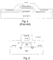
- FIG. 1 shows the FET 100 that was discussed by Hebiguchi.
- the transistor contains a glass substrate 110, a gate electrode 120, a gate insulating film 130, a drain electrode 140, a source electrode 150, and a semiconductor active film 160.
- voltage is applied to the source electrode 150 and to the gate electrode 120.
- the voltage applied to the gate electrode 120 changes the electrical properties of the semiconductor active film 160 allowing current to flow from the source electrode 150 to the drain electrode 140.
- the voltage applied to the gate electrode 120 creates a channel-generating region 170, in the semiconductor active film 160 a short distance from the gate insulating film 130, through which current may flow.
- the drain and source electrodes 140 and 150 are formed of conductive materials (metals) such as chromium (Cr), aluminum (Al), tantalum (Ta), platinum (Pt), gold (Au), tungsten (W), nickel (Ni), molybdenum (Mo), or certain mixtures of these materials, and the junctions between the semiconductor active film 160 and the source and drain electrodes 150 and 140 are insulating Schottky barriers.
- metal selected for an n-channel thin film transistor is chosen on the basis of having a workfunction that is smaller than that of silicon and the metal selected for a p-channel thin film transistor has a workfunction that is larger than that of silicon.
- Another type of junction to the channel is introduced by Yoshimura in U.S. Patent 6,037,605 ,with the stated goal being to reduce short-channel effects.
- An oxide or nitride is disposed between Si source and drain contacts and a Si channel.
- the oxide is thicker farther away from the channel (down into the Si) to reduce currents not controlled by the gate.
- the thickness of the oxide is "sufficiently thin to permit charge tunneling", and is disclosed to be 0.5 to 2.0 nm. This differs from the present invention, which is described in detail below, in several ways, for example the use of Si as a source/drain, as opposed to a metal.
- US 3,983,264 discloses forming a contact structure comprising an insulating film at the interface between the semiconductor surface and the metallization layer. A thickness of the insulating film below 1 nm is said to give unsatisfactory results.
- a transistor includes a semiconductor channel disposed nearby a gate (e.g., separated therefrom by a dielectric) and disposed in an electrical path between a source and a drain, wherein the channel and at least one of the source or the drain are separated by an interface layer of less than 1 nm so as to form a channel - interface layer - source/drain junction in which a Fermi level of the semiconductor channel is depinned in a region near the junction and the junction has a specific contact resistance of less than approximately 1000 ⁇ - ⁇ m 2 .
- the interface layer includes a passivating material which may be a nitride, a fluoride, an oxide, an oxynitride, a hydride and/or an arsenide of the semiconductor of the channel.
- the passivating material passivates said surface by covalently bonding with surface semiconductor atoms.
- the interface layer consists essentially of a monolayer configured to depin the Fermi level of the semiconductor of the channel, or an amount of passivation material sufficient to terminate all or a sufficient number of dangling bonds of the semiconductor channel to achieve chemical stability of the surface.
- the interface layer may include a separation layer of a material different than the passivating material. Where used, the separation layer has a thickness sufficient to reduce the effects of intrinsic surface states in the semiconductor channel.
- the above-cited co-pending patent application describes processes for depinning the Fermi level of a silicon-based or germanium semiconductor (e.g., Si, SiC, SiGe, SiGeC,or Ge) at a metal-semiconductor junction as well as devices that use such a junction.
- a silicon-based or germanium semiconductor e.g., Si, SiC, SiGe, SiGeC,or Ge
- an interface layer is introduced between the semiconductor and the metal.
- the interface layer functions to passivate the semiconductor surface (that is, terminate dangling bonds that may otherwise be present at the semiconductor surface so as to assure chemical stability of the surface) and to displace the semiconductor from the metal so as to reduce the effect of MIGS.
- minimum specific contact resistances of less than or equal to approximately 1000 ⁇ - ⁇ m 2 or less than or equal to approximately 100 ⁇ - ⁇ m 2 or less than or equal to approximately 50 ⁇ - ⁇ m 2 or less than or equal to approximately 10 ⁇ - ⁇ m 2 or even less than or equal to approximately 1 ⁇ - ⁇ m 2 may be achieved for such junctions in accordance with the present invention.
- a metal that has a work function near the conduction band of the semiconductor for n-type semiconductors, or a work function that is near the valence band for p-type semiconductors is selected.
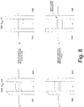
- FIG. 8 Shown in the illustration is a 2x2 grid of band diagrams.
- the upper two diagrams illustrate the operation of an n-type device having tunnel barriers (in the form of an interface layer configured in accordance with the present invention) and a metal source/drain in which the workfunction is aligned to the semiconductor channel conduction band under different gate voltages. Notice that the device is OFF (i.e., not conducting current) when the gate-to-source voltage (V GS ) is 0. The device is ON (i.e., conducting current) when V GS > 0.
- the lower two diagrams illustrate the operation of the n-type device having a metal source/drain in which the workfunction is aligned to the semiconductor channel mid-gap. Notice that even in the ON state ON (i.e., V GS > 0) a barrier to current flow exists due to band bending. This results in a higher contact resistance.
- the interface layers described in the above-cited patent application may be used in connection with a semiconductor surface of a channel in a FET, as discussed below. That is, an interface layer may be disposed between a source and a channel, a channel and a drain, or both of an insulated gate field effect transistor. Such use of an interface layer is described in detail herein.
- the present invention provides a source - channel and/or channel - drain contact wherein the Fermi level of the source and/or drain metal is aligned (or approximately aligned) with the conduction or valence band of the semiconductor, depending on the type of semiconductor material and metals used.
- the junction of the present invention can be used in making contacts to source or drain implanted wells and will have the advantage of reducing the need for high doping levels (which are now reaching their limits of solid solubility).
- the high doping profiles were required in the past in order to keep the junction depletion layer relatively thin, so as to increase the tunneling current, thus reducing the junction resistance.
- the present invention is used with high doping levels, the resistance will be further reduced.
- the present inventors have devised a scheme to passivate a semiconductor surface such as a channel surface within a Schottky barrier transistor.
- the scheme involves forming a passivation layer which is a nitride, hydride, oxide, arsenide and/or fluoride of the semiconductor that makes up the channel.
- a passivation layer which is a nitride, hydride, oxide, arsenide and/or fluoride of the semiconductor that makes up the channel.
- the term interface layer will be used in connection with the present invention to include passivation layers alone and passivation layers in combination with separation layers, where such separation layers are appropriate.
- the interface layer chemically neutralizes and physically protects the semiconductor channel surface.
- the interface layer also allows for a tunable Schottky barrier, having a height that depends on bulk characteristics of the channel semiconductor and the source/drain metal, rather than on surface properties. This allows greater control over the barrier height to meet the operational characteristics that are desired for the transistor.
- This scheme differs from past attempts by others to insulate channel surfaces and provide adjustable Schottky barriers in that the passivation materials used for the interface layer are not limited to metals that readily form silicides with the semiconductor channel.
- the present invention decouples the need for semiconductor passivation from other considerations used to select the source/drain metal, such as the desirability of a particular workfunction. It further provides for greater control of the Schottky-barrier height than previously possible.
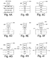
- FIG. 2 shows a transistor 200 formed on a substrate 210 (e.g., a semiconductor substrate such as Si or a compound substrate such as SOI) and configured in accordance with an embodiment of the present invention.
- the transistor 200 contains a channel 220 that is separated from a source 250 and a drain 260 by interface layers 230 and 240, respectively, each of which form passivated Schottky barriers.
- the particular transistor 200 shown, which is one example of a switching device, is an Insulated Gate FET.
- the interface layers 230 and 240 passivate the surfaces of channel 220 in the regions of the source/drain - channel junctions by chemically stabilizing the channel surface.
- the interface layers 230 and 240 also reduce or eliminate the effect of MIGS in the region of the source/drain - channel junctions by displacing the source/drain (250/260) away from the channel 220.
- the result of introducing the interface layers 230 and 240 between the semiconductor channel 220 and the metal source/drain 250/260 is a depinning of the Fermi level of the semiconductor that makes up channel 220.
- the height of the Schottky barrier will depend only on the difference of the bulk workfunctions of the metal and the semiconductor in contact at the junction, and will not be dependent upon the interface.
- the reduction in the effectiveness of the MIGS to pin the Fermi level depends on the choice of interface dielectric.
- MIGS metal-oxide-semiconductor
- dielectrics have much weaker MIGS than semiconductors, primarily due to larger bandgaps.
- the choice of dielectric is important in determining the final electrical characteristics of the Schottky barrier junction.
- the transistor 200 also includes a gate 270 surrounded by an insulator 280.
- the terms gate, source and drain each refer to terminals of a three terminal Insulated Gate FET.
- the source 250 and drain 260 are the terminals between which conduction occurs under the influence of an electric field resulting from a voltage applied to the gate 270.
- the source 250 and the drain 260 are provided at opposite ends of the channel 220 so that the channel 220 is disposed between the source 250 and the drain 260.
- the source 250 and drain 260 are fabricated such that they are geometrically symmetrical. Symmetrical source and drain terminals may be referred to as source/drain terminals.
- a particular terminal may be designated a source or a drain on the basis of the voltage to be applied to that terminal when the FET is operated in an electrical circuit.
- the source 250 is provided at a left-hand side of the channel 220 and the drain 260 is provided at a right-hand side of the channel 220, although another embodiment is contemplated wherein the source 250 and the drain 260 are interchanged.
- the source 250 and the drain 250 may each contain a conductor, preferably a metal.
- metals that may be used include pure metals, alloys, refractory metals, metals that do not form silicides, and metals having a predetermined work function.
- the gate 270 which may also preferably contain a conductor, such as a metal, is located above the channel 220 and is capacitively coupled to the channel 220 through the insulator 280. Note, in other embodiments the transistor's three terminals may be co-planar or the gate 270 may be disposed below the level of the source 250 and/or the drain 260 in the substrate 210.
- the insulator 280 (which may be made of a dielectric such as an oxide of the metal gate or an oxide of a semiconductor) surrounds the gate 270 and separates the gate 270 from the source 250, the drain 260, the channel 220, and the interface layers 230 and 240.
- the insulator 280 is of a sufficient thickness to provide a high resistance between the gate 270 and the channel 220 such that essentially no current flows between the gate 270 and the channel 220.
- the resistance may be between about 10 8 Ohms and about 10 12 Ohms, or greater. Such a resistance may allow the gate 270 and the channel 220 to be capacitively coupled, while preventing current from flowing between the gate 270 and the channel 220.
- the insulator 280 may also or alternatively contain a high-k dielectric material that has a higher dielectric constant than that of silicon dioxide (i.e., higher than about 4.0).
- the high-k material may allow the same charge induced in the channel 220 under the gate 270 to be achieved at the same gate voltage in a thicker layer. That is, the higher dielectric constant may allow the insulator 280 to have a greater layer thickness than a corresponding layer of silicon dioxide that provides the same amount of insulation. The increased thickness may simplify fabrication of the transistor 200.
- the thicker layer may also have less leakage current than a thinner SiO 2 layer.
- Exemplary high-k dielectric materials that are contemplated include materials having a dielectric constant greater than about 4 (e.g., zinc oxide, ZnO), greater than about 10 (e.g., aluminum oxide, Al 2 O 3 ), greater than about 20 (e.g., zirconium oxide, ZrO 2 ), and greater than about 40 (e.g., hafnium oxide, HfO).
- a dielectric constant greater than about 4 (e.g., zinc oxide, ZnO), greater than about 10 (e.g., aluminum oxide, Al 2 O 3 ), greater than about 20 (e.g., zirconium oxide, ZrO 2 ), and greater than about 40 (e.g., hafnium oxide, HfO).
- the channel 220 contains a semiconductor material.
- semiconductor is used to refer to a material having a bandgap that is greater than about 0.1 electron volts and less than about 4 electron volts.
- Exemplary semiconductors that are contemplated include Si, Ge, SiGe or SiC.
- the semiconductor material may have a wide range of doping levels including no doping at all.
- the interface layers 230 and 240 each contain a passivation material that provides passivation to the channel 220 by covalently bonding with a dangling bond of a surface semiconductor atom to fully coordinate the semiconductor atom and thereby help passivate the semiconductor atom.
- the passivation material is preferably selected from the group consisting of a hydride, a nitride, an arsenide, an oxide and a fluoride of the semiconductor channel 220.
- a separation layer in addition to a passivation layer within the interface layers 230 and 240 may be needed.
- the combination of the passivation layer and the separation layer must be sufficiently thin to permit the low specific contact resistances described in the above-cited patent application. Further details regarding the formation of an interface layer may be found in the above-cited patent application and will not be repeated herein.
- Figure 3 shows a method 300 for fabricating a transistor having passivated metal - semiconductor junctions from the source to the channel and from the channel to the drain, according to one embodiment of the present invention.
- the method starts at block 301 and then proceeds to block 310 where a substrate is provided.
- an insulated gate structure is formed on the substrate.
- the insulated gate structure may contain a gate having a conductive material (e.g., a metal) and a gate insulator having an insulating material beneath the conductive material.
- a channel is formed under the insulated gate.
- the channel may include undercut void regions subjacent the gate dielectric and extending into the channel on both ends of the insulated gate structure.
- the method advances to block 340 where an interface layer is formed on the channel sides.
- Forming the interface layer may include creating a passivating layer and (where necessary) a separation layer using one or more of the materials discussed above.
- the method then advances to block 350 where a source and drain are formed on opposite sides of the channel, including on the interface layer, and within any undercut regions. Depending upon the interface layer thickness and robustness, the source and drain may be formed by substantially non-invasive approaches.
- the method terminates at block 360.
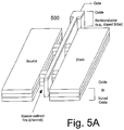
- Figures 4A-I show intermediate substrates, representing fabrication of the transistor shown in Figure 4I , according to one embodiment of the present invention.
- the particular transistor shown in Figure 4I contains passivated aluminum-silicon junctions 482I and 484I formed from the aluminum source 492I to the silicon channel 430I and from the silicon channel 430I to the aluminum drain 494I.
- this is merely one example of a transistor configured in accordance with the present invention.
- planar devices wherein the gate, source and drain are co-planar in or above the substrate are also within the scope of the present invention, as are embodiments where the gate is disposed in a plane below the source and/or drain.
- embodiments wherein the width of the gate is less than the width of the channel are included within the present invention.
- Figures 4A-I therefore show one embodiment of fabricating a transistor, according to the method 300.
- Figures 4A-4C show providing a substrate and forming an insulated gate on the substrate.
- Figures 4D-4E show forming a channel beneath the insulated gate, such that the channel and the insulated gate define a first and a second undercut void region that extend underneath the insulated gate toward the channel from a first and a second side of the insulated gate.
- Figure 4G shows forming an interface layer on exposed sidewall surfaces of the channel.
- Figures 4F, 4G, and 4H show forming a source and a drain terminal on a first and a second side of the channel including on the interface layers, and forming extension tips within the undercut voids beneath the insulated gate.
- Figure 4A shows a first intermediate substrate 400A containing a silicon substrate 410A, a layer of buried oxide of silicon 420A, a layer of silicon on insulator 430A, a layer of an oxide of silicon 440A, and an aluminum gate 450A.
- the layers 410A-430A represent a conventional Silicon On Insulator (SOI) substrate.
- SOI substrate includes the buried layer 440A to help isolate proximate semiconductor devices formed in the layer of silicon on insulator. This isolation may help reduce short-channel effects, as compared to semiconductor devices formed in a bulk wafer.
- the buried oxide layer may have a thickness that is effective to isolate the silicon on insulator, preferably greater than about 10 nm.
- the layer of silicon on insulator may have a thickness of about 20 nm, or slightly less.
- the SOI substrate is not a limitation of the present invention.
- Other substrates are contemplated to replace the SOI substrate.
- the SOI substrate may be replaced by a Silicon-On-Sapphire substrate, although this may increase the cost of fabrication, or the SOI substrate may be replaced by a plain silicon wafer, although this may provide inferior electrical isolation of semiconductor devices and poor short-channel characteristics.
- the layer of oxide of silicon 440A in one embodiment silicon dioxide (SiO 2 ), may be formed by wet or dry oxidation of the silicon on insulator, as is common in the semiconductor processing arts.
- the layer may be sufficiently thin to serve as a gate oxide and have a thickness between about 1 nm and about 10 nm.
- the aluminum gate 450A is formed on the oxide 440A.
- the aluminum gate has a width 451A that is about equal to, or slightly larger than the intended channel length, which in one embodiment is less than about 50 nm and in another embodiment is less than about 20 nm. More than slight increases of the width over the channel length may increase the extent and angle of a subsequent undercut etch, which may complicate fabrication.
- the gate450A may be formed by depositing a layer of aluminum on the oxide 440A, depositing a photoresist layer on the deposited aluminum layer, exposing a pattern including the width 451A in the photoresist using conventional high-resolution lithography, removing a portion of the photoresist according to the exposed pattern, wet or dry etching a portion of the deposited layer of aluminum according to the patterned photoresist, and removing the remaining photoresist.
- Figure 4B shows a second intermediate substrate 400B containing an oxide of aluminum insulator 460B formed on exposed portions, including the top and sides, of the aluminum gate 450B.
- the oxide of aluminum layer 460B may have a thickness between about 1 nm and about 20 nm. The thickness may be about equivalent to the thickness of the layer 440B, or slightly larger. Larger thickness may improve performance by reducing capacitance between the gate and the source, however the additional thickness may also increase fabrication complexity by increasing undercut.
- Forming the oxide of aluminum layer 460B may include oxidizing the aluminum gate 450A in an oxygen plasma etcher that provides a suitable oxidizing atmosphere, or by other methods known in the semiconductor processing arts.
- Figure 4C shows a third intermediate substrate 400C containing a gate oxide 440C formed by removing a portion of the layer 440B that is not beneath aluminum gate 450B or aluminum oxide 460B.
- the removal may include using the oxidized aluminum gate 450B-460B as a mask for the layer 440B and etching portions of the layer 440B that are not subjacent to and concealed by the oxidized aluminum gate 450B-460B. This removal leaves a portion of the silicon on insulator layer 430C that is not subjacent to the gate oxide 440C, aluminum gate 450C, or oxide 460C exposed.
- Etching may include Reactive Ion Etching (RIE) to encourage etching preferentially in the direction normal or perpendicular to the surface of the layer 440B.
- RIE Reactive Ion Etching
- RIE is a dry-etch process wherein the intermediate substrate 400B is placed on a radio frequency powered electrode and provided with a potential that helps ionize and accelerate ion bombardment of etching species extracted from plasma toward the etched surface.
- Figure 4D shows a fourth intermediate substrate 400D containing a silicon channel 430D formed by removing a portion of the silicon on insulator layer 430C that is substantially not subjacent and concealed by the gate oxide 440C. Removal may include etching silicon on insulator that has a standard Si-100 orientation with tetramethylammonium hydroxide (TMAH) to form angled sidewalls that slope inward toward the gate 450D, as shown. Alternatively, comparatively straight sidewalls aligned with the gate oxide 440D may be formed by a self-limiting etch in TMAH if the silicon on insulator has a Si-110 orientation. Such comparatively straight sidewalls may also be formed by RIE.
- TMAH tetramethylammonium hydroxide
- Figure 4E shows a fifth intermediate substrate 400E containing an undercut silicon channel 430E formed by removing a portion of the channel 430D that is subjacent and aligned with the gate oxide 440D.
- the undercut silicon channel 430E contains an undercut region wherein the silicon is removed from the channel 430D at a left and right-hand edge of the gate oxide 440D to allow a subsequent formation of source and drain material vertically under the gate oxide 440E. Removal may be by a non-directional or isotropic wet silicon etch with TMAH wherein etching takes place in substantial uniform amounts along the sidewall.
- the TMAH etch may not be completely self-limiting and may form an undercut due to the vertical ridges or stair steps of crystal structure.
- removal may be by an isotropic RIE.
- Figure 4F shows a sixth intermediate substrate 400F containing a seed layer 476F, 472F, and 474F formed respectively on a top surface of the insulated gate and on a left and right-hand side of the insulated gate.
- the seed layer facilitates subsequent formation of a metal source and drain.
- the seed layer may be deposited anisotropically so that no significant seed layer material is deposited on the vertical sidewalls of the aluminum oxide 460F, gate oxide 440F, or channel 430F and essentially no metal is deposited on the underside of the undercut overhang of the gate oxide 440F. This is desired to electrically isolate the seed layer portion 476F from the seed layer portion 472F and 474F.
- the seed layer contains chromium deposited from a thermal source. Chromium provides desirable electrochemistry and is well suited for formation of ultra-thin films.
- Figure 4G shows a seventh intermediate substrate 400G containing a modified seed layer 472G-474G formed by selectively removing the layer portion 476F from the top surface of the insulated gate. Removal of the portion 476F is desirable to allow depositing the source and drain materials superjacent the layer portions 472G and 476G without depositing the source and drain materials atop the oxidized aluminum gate structure. Since the seed layer portion 476F is electrically isolated from the seed layer portions 472F and 476F, the portion 476F may be removed electrochemically by a Cerric Ammonium Nitrate (CAN) chrome etch.
- CAN Cerric Ammonium Nitrate
- the seed layer portions 472F and 474F but not the seed layer portion 476F may be electrically coupled with a copper electrical probe at the edge of the substrate to etch the seed layer portion 476F but not the portions 472F-474F.
- patterning may be used to form chromium layers 472F and 474F without forming chromium layer 476F. This may avoid a subsequent removal of the chromium layer 476F.
- Figure 4H shows an eighth intermediate substrate 400H containing interface layers 482H and 484H formed on the sidewall surfaces of the channel 430H.
- the interface layers may be a monolayer, slightly more than a monolayer, less than about 0.3 nm, less than about 0.5 nm or less than about 1 nm (depending upon the desired Schottky barrier characteristics). That is, in some cases an amount of passivation material sufficient to terminate all or a sufficient number of dangling bonds of the semiconductor channel to achieve chemical stability of the surface may be used.
- the interface layers may be grown in accordance with the techniques discussed in the above-cited patent application. Passivation materials that are contemplated include arsenic, hydrogen, fluorine, oxygen, and nitrogen, as discussed above, and the interface layers 482H and 484H may be made up of both a passivation layer and a separation layer.
- Figure 4I shows a ninth intermediate substrate 400I containing a source 492I formed superjacent upon the seed material 472H and beneath the left undercut overhang and a drain 494I formed superjacent upon the seed material 474H and beneath the right undercut overhang.
- the source and drain have a thickness that extends above the gate insulator 440I. Desirably, the thickness may be precisely controlled. Forming may include plating the potentially different source/drain materials on the seed layers 472H and 474H.
- This may include depositing a photoresist, irradiating the photoresist to expose a channel width pattern, removing a portion of the photoresist to expose the seed layers 472H and 474H, plating the source/drain materials on the seed layers 472H and 474H, and removing the remainder of the photoresist.
- the source and drain materials are aluminum.
- the source and drain materials may be another desired and potentially different metal or alloy.
- the transistor shown in Figure 4I has a number of advantages.
- the transistor provides a simple construction. This may allow extending transistor fabrication below 50 nm channel lengths, below 20 nm channel lengths, or even below 10 nm channel lengths.
- Another advantage is greater control over the Schottky barrier height provided by the interface layers.
- the barrier height may be controlled by the properties of the interface layer such as passivation material, layer thickness, and layer formation conditions, in addition to difference in workfunctions between the source/drain and the channel. This ability to control the barrier height is further increased by greater flexibility in selecting source/drain materials, since, due to the interface layers, the source/drain materials do not have to readily form silicides with the silicon channel.
- the channel - interface layer - source/drain junction(s) of the transistor shown in Figure 4I are unique in that the Fermi level of the semiconductor channel is depinned in a region near the junction and the junction has a specific contact resistance of less than approximately 1000 ⁇ - ⁇ m 2 . This is true of all transistors configured in accordance with the present invention. Indeed, minimum specific contact resistances of less than or equal to approximately 10 ⁇ - ⁇ m 2 or even less than or equal to approximately 1 ⁇ - ⁇ m 2 may be achieved for such junctions in accordance with the present invention.
- a source/drain metal that has a work function near the conduction band of the semiconductor for n-type semiconductors, or a work function that is near the valence band for p-type semiconductors, is selected.
- the depinning role played by the interface layer in tuning, adjusting, or controlling the height of the barrier between the source/drain and the semiconductor channel involves both a reduction in surface states of the channel, by bonding to the semiconductor material to consume dangling bonds, a reduction in the formation of MIGS in the semiconductor channel, by providing a thickness and bandgap that prevent the electron wave function (of the source/drain metal) from penetrating into the semiconductor channel.
- the electron wave function may instead penetrate into the interface layer and form MIGS within the interface layer at an energy related to the states of the interface layer material.
- the density of the MIGS and the depth of MIGS penetration into the interface layer may be reduced by choosing an interface layer material or materials having a larger bandgap or higher effective mass than the semiconductor of the channel.
- the interface layer is operable to pass current to/from the semiconductor channel during device operation.
- an interface layer having a thickness of a monolayer, or, for example between about 0.1 nm and about 0.3 nm, and also having a wide bandgap (as compared to that of the semiconductor of the channel) so that the interface layer both depins the Fermi level (so that the barrier height depends predominantly on bulk properties of the junction materials) and allows sufficient current transfer across it.
- the interface layer may include only an amount of passivation material sufficient to terminate all or a sufficient number of dangling bonds of the semiconductor channel to achieve chemical stability of the surface.
- such interface layers may be sufficiently thin to provide low impedance to current flow (due to the exponential dependence of direct tunneling on barrier thickness), which is desirable for many semiconductor devices, while also providing sufficient semiconductor surface passivation to allow an adjustable barrier height. That is, the interface layer may allow passivation of surface states and reduction (or elimination) of MIGS in the semiconductor to allow for an adjustable barrier height with a substantially thin layer that allows sufficient current to be transferred across the interface layer.
- the barrier height can be made adjustable.
- adjustment may be made by tuning the degree of Fermi level pinning.
- some embodiments may allow for a sufficiently thin interface layer so that not all of the effects of MIGS in the semiconductor channel are eliminated.
- the pinning may be varied by combinations of thickness of the interface layer and the choice of interface material.
- the metal in contact with the interface layer may be pinned by MIGS at different levels in different materials.
- the semiconductor channel passivation may be left incomplete to allow for an effective level of unpassivated states.
- Complete depinning of the Fermi level that is removal of all surface states in the semiconductor channel including MIGS is another option, in which case one could tune the barrier height simply by choosing a pure metal or an alloy that possesses the desired workfunction.
- one embodiment for fabricating a transistor on a semiconductor substrate includes: (1) forming a semiconductor oxide dielectric layer on a semiconductor substrate by oxidizing the semiconductor substrate; (2) forming a metal gate on the semiconductor oxide layer by depositing a layer of metal on the semiconductor oxide and removing a portion of the deposited layer of metal based on a lithographic exposure; (3) forming a metal oxide dielectric layer on exposed portions of the metal gate by oxidizing the metal gate; (4) forming a gate oxide dielectric by removing a portion of the semiconductor oxide layer that is protected by the metal oxide formed on the metal gate; (5) forming a semiconductor channel structure by removing a portion of the semiconductor substrate that is not protected by the metal oxide formed on the metal gate; (6) forming an undercut semiconductor channel containing a source undercut region for a source tip and a drain undercut region for a drain tip by removing a source tip portion of the semiconductor channel structure that is subjacent to a left-hand end of the gate oxide and extends underneath the gate oxide toward the channel top
- the transistor illustrated in Figure 4I is but one example of the types of FETs that can benefit from the present invention.
- Other FETs known in the art may also realize such benefits by incorporating the present interface layers into source/drain - channel junctions.
- so-called FinFETs may incorporate such interface layers.
- a FinFET is an example of a thin-body SOI device and is the name given to a class of FETs developed by researchers at the University of California, Berkely.
- Conventional FinFETs are described in detail in Yang-Kyu Choi et al., "Nanoscale CMOS Spacer FinFET for the Terabit Era", IEEE Electron Device Letters, vol. 25, no. 1 (Jan. 2002 ), incorporated herein by reference, and an example of such a device 500 is illustrated in Figure 5A .
- the channel of a finFET is formed by spacer-defined semiconductor fins.
- FIG. 5B shows a Fin-FET 520 modified to incorporate interface layers 522 in accordance with an embodiment of the present invention.
- the semiconductor source and/or drain are replaced with a metal source and/or drain.
- the semiconductor fins i.e., the channel
- the semiconductor fins contact these source/drain regions through an interface layer.
- FIG. 6A Another transistor where the present invention may find application is the so-called vertical MOSFET, e.g., as described in E. Josse et al., "High performance 40 nm vertical MOSFET within a conventional CMOS process flow", 2001 Symposium on VLSI Technology Digest of Technical Papers. Paper No. 5B-2, pages 55 - 56 (2001 ), incorporated herein by reference.
- Vertical MOSFETs are characterized by a pillar-like channel sandwiched between a double gate. The source and drain are located at the ends of the channel pillar. An example of such a structure 600 is shown in Figure 6A .
- FIG. 6B shows a vertical MOSFET 620 modified to incorporate interface layers in accordance with an embodiment of the present invention.
- This transistor is similar to the MOSFET illustrated in Figure 6A but the upper Si n-region (the drain in this example) has been replace with a metal drain and contact to the channel is through an interface layer 622.
- such devices may be asymmetric, having a passivated Si/metal tunnel junction at the top contact, and a Si p-n junction at the bottom of the device on the substrate side.
- Complementary devices may be fabricated on the same substrate by first implanting p and n regions for the bottom contacts, and then employing two different metals, each with work functions chosen to yield p-type or n-type devices, as the top contacts to the channel.
- FIG. 7A illustrates yet another type of transistor 700, the MESFET.
- a MESFET Metal Semiconductor FET
- the conductance of the channel is modulated when an applied gate voltage results in a change in the depletion width of the Schottky barrier into the channel.
- the channel as shown may be a thin Si layer, as in an SOI substrate.
- the Schottky barrier For optimizing the utility of a particular MESFET application, it may be desirable to either raise or lower the Schottky barrier. This may be achieved as shown in Figure 7B by implementation of the present invention in a transistor 720 wherein a particular interface dielectric and contact metal may be appropriately chosen.
- the interface dielectric forms an interface layer 722 between the gate and the channel.
- the gate may be poly Si instead of a metal.
- Transistors such as those described herein may be used in chips, integrated circuits, monolithic devices, semiconductor devices, microelectronic devices, and the like within a number of electrical systems. Electrical systems that are contemplated include computer systems (e.g., portable, laptop, desktop, server, mainframe, etc.), hard copy equipment (e.g., printer, plotter, fax machine, etc.), and other electrical systems.
- a computer system may comprise a microprocessor having such a transistor to help execute instructions.
- the computer system may contain other conventional components including but not limited to a bus or other communication means to communicate information, a memory to store information (e.g., a dynamic memory such as RAM or a static memory such as ROM), a display device, a data input device, and a communication device such as a modem, as will be appreciated by a person having an ordinary level of skill in the art and the benefit of the present disclosure. Any or all of these devices may include transistors configured in accordance with the present invention.
Claims (16)
- Transistor (200) comprenant un canal à semi-conducteur à base de silicium ou de germanium (220) disposé (i) à proximité d'une grille (270) configurée pour réguler la conductance dans le canal et (ii) dans un trajet électrique entre une source (250) et un drain (260), dont au moins un(e) est réalisé(e) en un métal, où le canal et n'importe lequel/laquelle de la source et/du drain qui est réalisé(e) en le métal sont séparés par une couche d'interface (230, 240) inférieure à 1 nm de manière à former une jonction canal-couche d'interface-source/drain dans laquelle un niveau de Fermi du canal à semi-conducteur est décalé dans une région proche de la jonction, la jonction comportant une surface semi-conductrice passivée par un matériau de passivation de la couche d'interface, le matériau de passivation passivant ladite surface par liaison covalente avec des atomes semi-conducteurs de surface, la jonction ayant une résistance de contact spécifique inférieure à environ 1000 Ω-µm2.
- Transistor de la revendication 1, dans lequel le canal à semi-conducteur est réalisé en un élément entre Si, Ge, SiGe, SiGeC et SiC.
- Transistor de la revendication 1, dans lequel le métal comprend l'un d'un métal pur, d'un alliage et d'un métal réfractaire.
- Transistor de la revendication 1, dans lequel le métal comprend de l'aluminium.
- Transistor de la revendication 1, dans lequel la couche d'interface a une épaisseur inférieure à 0,5 nm.
- Transistor de la revendication 1, dans lequel la couche d'interface a une épaisseur inférieure à 0,3 nm.
- Transistor de la revendication 1, dans lequel la couche d'interface a une épaisseur comprise entre 0,1 et 0,3 nm.
- Transistor de la revendication 1, dans lequel la couche d'interface est une monocouche.
- Transistor de la revendication 1, dans lequel le matériau de passivation comprend un ou plusieurs élément(s) d'un nitrure du semi-conducteur du canal, d'un fluorure du semi-conducteur du canal, d'un oxyde du semi-conducteur du canal, d'un oxynitrure du semi-conducteur du canal, d'un hydrure du semi-conducteur du canal et/ou d'un arséniure du semi-conducteur du canal.
- Transistor de la revendication 9, dans lequel la couche d'interface consiste essentiellement en une quantité de matériau de passivation suffisante pour terminer suffisamment de liaisons pendantes d'une surface du canal à semi-conducteur afin d'obtenir une stabilité chimique de la surface.
- Transistor de la revendication 9, dans lequel la couche d'interface consiste essentiellement en une monocouche configurée pour décaler le niveau de Fermi du semi-conducteur du canal.
- Transistor de la revendication 11, dans lequel la couche d'interface a une épaisseur suffisante pour réduire les effets des états d'intervalles induits par un métal dans le canal à semi-conducteur.
- Transistor de la revendication 1, dans lequel la couche d'interface comporte en outre une couche de séparation.
- Transistor de la revendication 13, dans lequel la couche de séparation a une épaisseur suffisante pour réduire les effets des états d'intervalles induits par un métal dans le canal à semi-conducteur.
- Transistor de la revendication 1, dans lequel le canal à semi-conducteur est séparé de la grille par un diélectrique.
- Transistor de la revendication 1, dans lequel la couche d'interface comprend une monocouche de matériau de passivation.
Applications Claiming Priority (5)
| Application Number | Priority Date | Filing Date | Title |
|---|---|---|---|
| US217758 | 1988-07-11 | ||
| US10/217,758 US7084423B2 (en) | 2002-08-12 | 2002-08-12 | Method for depinning the Fermi level of a semiconductor at an electrical junction and devices incorporating such junctions |
| US342576 | 2003-01-14 | ||
| US10/342,576 US6833556B2 (en) | 2002-08-12 | 2003-01-14 | Insulated gate field effect transistor having passivated schottky barriers to the channel |
| PCT/US2003/025057 WO2004015782A1 (fr) | 2002-08-12 | 2003-08-08 | Transistor a effet de champ a grille isolee presentant des barrieres de schottky passivees vers le canal |
Publications (2)
| Publication Number | Publication Date |
|---|---|
| EP1535343A1 EP1535343A1 (fr) | 2005-06-01 |
| EP1535343B1 true EP1535343B1 (fr) | 2019-08-07 |
Family
ID=31720178
Family Applications (1)
| Application Number | Title | Priority Date | Filing Date |
|---|---|---|---|
| EP03785158.1A Expired - Lifetime EP1535343B1 (fr) | 2002-08-12 | 2003-08-08 | Transistor a effet de champ a grille isolee presentant des barrieres de schottky passivees vers le canal |
Country Status (8)
| Country | Link |
|---|---|
| US (7) | US6833556B2 (fr) |
| EP (1) | EP1535343B1 (fr) |
| JP (1) | JP4713884B2 (fr) |
| KR (1) | KR101018103B1 (fr) |
| CN (1) | CN100557816C (fr) |
| AU (1) | AU2003255257A1 (fr) |
| TW (2) | TWI310608B (fr) |
| WO (1) | WO2004015782A1 (fr) |
Families Citing this family (141)
| Publication number | Priority date | Publication date | Assignee | Title |
|---|---|---|---|---|
| US6303479B1 (en) * | 1999-12-16 | 2001-10-16 | Spinnaker Semiconductor, Inc. | Method of manufacturing a short-channel FET with Schottky-barrier source and drain contacts |
| US7190008B2 (en) | 2002-04-24 | 2007-03-13 | E Ink Corporation | Electro-optic displays, and components for use therein |
| US6835619B2 (en) * | 2002-08-08 | 2004-12-28 | Micron Technology, Inc. | Method of forming a memory transistor comprising a Schottky contact |
| US6833556B2 (en) | 2002-08-12 | 2004-12-21 | Acorn Technologies, Inc. | Insulated gate field effect transistor having passivated schottky barriers to the channel |
| US7084423B2 (en) | 2002-08-12 | 2006-08-01 | Acorn Technologies, Inc. | Method for depinning the Fermi level of a semiconductor at an electrical junction and devices incorporating such junctions |
| US7176483B2 (en) * | 2002-08-12 | 2007-02-13 | Acorn Technologies, Inc. | Method for depinning the Fermi level of a semiconductor at an electrical junction and devices incorporating such junctions |
| US7902029B2 (en) * | 2002-08-12 | 2011-03-08 | Acorn Technologies, Inc. | Process for fabricating a self-aligned deposited source/drain insulated gate field-effect transistor |
| KR100498475B1 (ko) * | 2003-01-07 | 2005-07-01 | 삼성전자주식회사 | 모스 전계 효과 트랜지스터 구조 및 그 제조 방법 |
| US20070262363A1 (en) * | 2003-02-28 | 2007-11-15 | Board Of Regents, University Of Texas System | Low temperature fabrication of discrete silicon-containing substrates and devices |
| KR100508548B1 (ko) * | 2003-04-16 | 2005-08-17 | 한국전자통신연구원 | 쇼트키 장벽 트랜지스터 및 그 제조방법 |
| US6894326B2 (en) | 2003-06-25 | 2005-05-17 | International Business Machines Corporation | High-density finFET integration scheme |
| US7456476B2 (en) | 2003-06-27 | 2008-11-25 | Intel Corporation | Nonplanar semiconductor device with partially or fully wrapped around gate electrode and methods of fabrication |
| US6909151B2 (en) | 2003-06-27 | 2005-06-21 | Intel Corporation | Nonplanar device with stress incorporation layer and method of fabrication |
| US6995376B2 (en) * | 2003-07-01 | 2006-02-07 | International Business Machines Corporation | Silicon-on-insulator latch-up pulse-radiation detector |
| KR100496891B1 (ko) * | 2003-08-14 | 2005-06-23 | 삼성전자주식회사 | 핀 전계효과 트랜지스터를 위한 실리콘 핀 및 그 제조 방법 |
| JP2005064500A (ja) * | 2003-08-14 | 2005-03-10 | Samsung Electronics Co Ltd | マルチ構造のシリコンフィンおよび製造方法 |
| JP4439358B2 (ja) * | 2003-09-05 | 2010-03-24 | 株式会社東芝 | 電界効果トランジスタ及びその製造方法 |
| JP2005086024A (ja) * | 2003-09-09 | 2005-03-31 | Toshiba Corp | 半導体装置及びその製造方法 |
| US6855588B1 (en) * | 2003-10-07 | 2005-02-15 | United Microelectronics Corp. | Method of fabricating a double gate MOSFET device |
| US20050139860A1 (en) * | 2003-10-22 | 2005-06-30 | Snyder John P. | Dynamic schottky barrier MOSFET device and method of manufacture |
| US7166867B2 (en) | 2003-12-05 | 2007-01-23 | International Rectifier Corporation | III-nitride device with improved layout geometry |
| US8217450B1 (en) * | 2004-02-03 | 2012-07-10 | GlobalFoundries, Inc. | Double-gate semiconductor device with gate contacts formed adjacent sidewalls of a fin |
| KR100574971B1 (ko) * | 2004-02-17 | 2006-05-02 | 삼성전자주식회사 | 멀티-게이트 구조의 반도체 소자 및 그 제조 방법 |
| US7923782B2 (en) * | 2004-02-27 | 2011-04-12 | International Business Machines Corporation | Hybrid SOI/bulk semiconductor transistors |
| US7154118B2 (en) | 2004-03-31 | 2006-12-26 | Intel Corporation | Bulk non-planar transistor having strained enhanced mobility and methods of fabrication |
| US7504328B2 (en) * | 2004-05-11 | 2009-03-17 | National University Of Singapore | Schottky barrier source/drain n-mosfet using ytterbium silicide |
| US7229893B2 (en) * | 2004-06-23 | 2007-06-12 | Taiwan Semiconductor Manufacturing Company, Ltd. | Method and apparatus for a semiconductor device with a high-k gate dielectric |
| JP4837902B2 (ja) | 2004-06-24 | 2011-12-14 | 富士通セミコンダクター株式会社 | 半導体装置 |
| US7042009B2 (en) | 2004-06-30 | 2006-05-09 | Intel Corporation | High mobility tri-gate devices and methods of fabrication |
| US7365015B2 (en) * | 2004-07-13 | 2008-04-29 | Lsi Logic Corporation | Damascene replacement metal gate process with controlled gate profile and length using Si1-xGex as sacrificial material |
| JP2006054423A (ja) * | 2004-07-13 | 2006-02-23 | Toshiba Corp | 半導体装置及びその製造方法 |
| US7279756B2 (en) * | 2004-07-21 | 2007-10-09 | Taiwan Semiconductor Manufacturing Company, Ltd. | Semiconductor device with high-k gate dielectric and quasi-metal gate, and method of forming thereof |
| US7598134B2 (en) | 2004-07-28 | 2009-10-06 | Micron Technology, Inc. | Memory device forming methods |
| US7348284B2 (en) | 2004-08-10 | 2008-03-25 | Intel Corporation | Non-planar pMOS structure with a strained channel region and an integrated strained CMOS flow |
| US7345309B2 (en) * | 2004-08-31 | 2008-03-18 | Lockheed Martin Corporation | SiC metal semiconductor field-effect transistor |
| US7527994B2 (en) * | 2004-09-01 | 2009-05-05 | Honeywell International Inc. | Amorphous silicon thin-film transistors and methods of making the same |
| US7078722B2 (en) * | 2004-09-20 | 2006-07-18 | International Business Machines Corporation | NFET and PFET devices and methods of fabricating same |
| JP2006100600A (ja) * | 2004-09-29 | 2006-04-13 | Toshiba Corp | 半導体装置およびその製造方法 |
| US7422946B2 (en) | 2004-09-29 | 2008-09-09 | Intel Corporation | Independently accessed double-gate and tri-gate transistors in same process flow |
| US7332439B2 (en) | 2004-09-29 | 2008-02-19 | Intel Corporation | Metal gate transistors with epitaxial source and drain regions |
| US20060086977A1 (en) | 2004-10-25 | 2006-04-27 | Uday Shah | Nonplanar device with thinned lower body portion and method of fabrication |
| US20060091467A1 (en) * | 2004-10-29 | 2006-05-04 | Doyle Brian S | Resonant tunneling device using metal oxide semiconductor processing |
| US7355235B2 (en) * | 2004-12-22 | 2008-04-08 | Taiwan Semiconductor Manufacturing Company, Ltd. | Semiconductor device and method for high-k gate dielectrics |
| US7332407B2 (en) * | 2004-12-23 | 2008-02-19 | Taiwan Semiconductor Manufacturing Company, Ltd. | Method and apparatus for a semiconductor device with a high-k gate dielectric |
| US7078285B1 (en) * | 2005-01-21 | 2006-07-18 | Sony Corporation | SiGe nickel barrier structure employed in a CMOS device to prevent excess diffusion of nickel used in the silicide material |
| US7518196B2 (en) | 2005-02-23 | 2009-04-14 | Intel Corporation | Field effect transistor with narrow bandgap source and drain regions and method of fabrication |
| US7271457B2 (en) * | 2005-03-04 | 2007-09-18 | Bae Systems Information And Electronic Systems Integration Inc. | Abrupt channel doping profile for fermi threshold field effect transistors |
| FR2883101B1 (fr) * | 2005-03-08 | 2007-06-08 | Centre Nat Rech Scient | Transistor mos nanometrique a rapport maximise entre courant a l'etat passant et courant a l'etat bloque |
| US20060202266A1 (en) | 2005-03-14 | 2006-09-14 | Marko Radosavljevic | Field effect transistor with metal source/drain regions |
| US7329937B2 (en) * | 2005-04-27 | 2008-02-12 | International Business Machines Corporation | Asymmetric field effect transistors (FETs) |
| US7176537B2 (en) * | 2005-05-23 | 2007-02-13 | Taiwan Semiconductor Manufacturing Company, Ltd. | High performance CMOS with metal-gate and Schottky source/drain |
| US7858481B2 (en) | 2005-06-15 | 2010-12-28 | Intel Corporation | Method for fabricating transistor with thinned channel |
| US7547637B2 (en) | 2005-06-21 | 2009-06-16 | Intel Corporation | Methods for patterning a semiconductor film |
| US7279375B2 (en) | 2005-06-30 | 2007-10-09 | Intel Corporation | Block contact architectures for nanoscale channel transistors |
| US20070001223A1 (en) * | 2005-07-01 | 2007-01-04 | Boyd Diane C | Ultrathin-body schottky contact MOSFET |
| US7402875B2 (en) | 2005-08-17 | 2008-07-22 | Intel Corporation | Lateral undercut of metal gate in SOI device |
| US20070090416A1 (en) | 2005-09-28 | 2007-04-26 | Doyle Brian S | CMOS devices with a single work function gate electrode and method of fabrication |
| US7479421B2 (en) | 2005-09-28 | 2009-01-20 | Intel Corporation | Process for integrating planar and non-planar CMOS transistors on a bulk substrate and article made thereby |
| US7485503B2 (en) | 2005-11-30 | 2009-02-03 | Intel Corporation | Dielectric interface for group III-V semiconductor device |
| KR100777101B1 (ko) * | 2005-12-07 | 2007-11-19 | 한국전자통신연구원 | 낮은 쇼트키 장벽 관통 트랜지스터 및 그 제조방법 |
| JP2007165772A (ja) * | 2005-12-16 | 2007-06-28 | Toshiba Corp | 半導体装置および半導体装置の製造方法 |
| US7432526B2 (en) * | 2005-12-20 | 2008-10-07 | Palo Alto Research Center Incorporated | Surface-passivated zinc-oxide based sensor |
| WO2007080576A1 (fr) * | 2006-01-09 | 2007-07-19 | Technion Research And Development Foundation Ltd. | Structures de transistor et procedes de fabrication de celles-ci |
| US7473593B2 (en) * | 2006-01-11 | 2009-01-06 | International Business Machines Corporation | Semiconductor transistors with expanded top portions of gates |
| FR2897202B1 (fr) * | 2006-02-08 | 2008-09-12 | St Microelectronics Crolles 2 | Transistor mos a barriere de schottky sur film semi-conducteur entierement appauvri et procede de fabrication d'un tel transistor. |
| WO2007101120A1 (fr) * | 2006-02-23 | 2007-09-07 | Acorn Technologies, Inc. | Procédé permettant de fabriquer un transistor à effet de champ à grille isolée semi-conducteur présentant plusieurs couches de source(s) et/ou de drain(s) métalliques déposées |
| JP2007299951A (ja) * | 2006-04-28 | 2007-11-15 | Toshiba Corp | 半導体装置およびその製造方法 |
| US8435873B2 (en) | 2006-06-08 | 2013-05-07 | Texas Instruments Incorporated | Unguarded Schottky barrier diodes with dielectric underetch at silicide interface |
| US7485524B2 (en) * | 2006-06-21 | 2009-02-03 | International Business Machines Corporation | MOSFETs comprising source/drain regions with slanted upper surfaces, and method for fabricating the same |
| US20080023752A1 (en) * | 2006-07-28 | 2008-01-31 | International Business Machines Corporation | BORON DOPED SiGe HALO FOR NFET TO CONTROL SHORT CHANNEL EFFECT |
| US8143646B2 (en) | 2006-08-02 | 2012-03-27 | Intel Corporation | Stacking fault and twin blocking barrier for integrating III-V on Si |
| US7646046B2 (en) * | 2006-11-14 | 2010-01-12 | Infineon Technologies Ag | Field effect transistor with a fin structure |
| US20080258242A1 (en) * | 2007-04-19 | 2008-10-23 | Northrop Grumman Space And Mission Systems Corp. | Low contact resistance ohmic contact for a high electron mobility transistor and fabrication method thereof |
| JP2008288499A (ja) * | 2007-05-21 | 2008-11-27 | Panasonic Corp | 半導体装置及びその製造方法 |
| JP5108408B2 (ja) * | 2007-07-26 | 2012-12-26 | ルネサスエレクトロニクス株式会社 | 半導体装置及びその製造方法 |
| JP2009059996A (ja) * | 2007-09-03 | 2009-03-19 | Univ Of Tokyo | 半導体装置及びその製造方法 |
| KR100945508B1 (ko) | 2007-11-16 | 2010-03-09 | 주식회사 하이닉스반도체 | 제로 캐패시터 램 및 그의 제조방법 |
| US8362566B2 (en) | 2008-06-23 | 2013-01-29 | Intel Corporation | Stress in trigate devices using complimentary gate fill materials |
| US8110877B2 (en) * | 2008-12-19 | 2012-02-07 | Intel Corporation | Metal-insulator-semiconductor tunneling contacts having an insulative layer disposed between source/drain contacts and source/drain regions |
| JP4752927B2 (ja) * | 2009-02-09 | 2011-08-17 | ソニー株式会社 | 薄膜トランジスタおよび表示装置 |
| JP5210915B2 (ja) * | 2009-02-09 | 2013-06-12 | 株式会社東芝 | 半導体装置の製造方法 |
| WO2010113715A1 (fr) * | 2009-03-31 | 2010-10-07 | 日鉱金属株式会社 | Procédé de fabrication d'un dispositif à semi-conducteurs et dispositif à semi-conducteurs |
| US8288803B2 (en) * | 2009-08-31 | 2012-10-16 | International Business Machines Corporation | Tunnel field effect devices |
| US9059318B2 (en) | 2009-08-31 | 2015-06-16 | International Business Machines Corporation | Stressed source/drain CMOS and method of forming same |
| US20110049582A1 (en) * | 2009-09-03 | 2011-03-03 | International Business Machines Corporation | Asymmetric source and drain stressor regions |
| US8669644B2 (en) * | 2009-10-07 | 2014-03-11 | Texas Instruments Incorporated | Hydrogen passivation of integrated circuits |
| JP5640379B2 (ja) * | 2009-12-28 | 2014-12-17 | ソニー株式会社 | 半導体装置の製造方法 |
| KR101121633B1 (ko) * | 2009-12-30 | 2012-03-09 | 주식회사 하이닉스반도체 | 반도체 장치 및 그 제조방법 |
| US8492234B2 (en) * | 2010-06-29 | 2013-07-23 | International Business Machines Corporation | Field effect transistor device |
| JP2012114173A (ja) * | 2010-11-23 | 2012-06-14 | Shinko Electric Ind Co Ltd | 半導体装置の製造方法及び半導体装置 |
| US9166004B2 (en) * | 2010-12-23 | 2015-10-20 | Intel Corporation | Semiconductor device contacts |
| US9023684B2 (en) * | 2011-03-04 | 2015-05-05 | Semiconductor Energy Laboratory Co., Ltd. | Semiconductor device and manufacturing method thereof |
| CN102148255B (zh) * | 2011-03-15 | 2013-07-31 | 清华大学 | 具有隧穿介质层的栅控肖特基结场效应晶体管及形成方法 |
| JP5360119B2 (ja) * | 2011-04-18 | 2013-12-04 | 富士通セミコンダクター株式会社 | 半導体装置とその製造方法 |
| JP5455973B2 (ja) | 2011-05-27 | 2014-03-26 | 三菱電機株式会社 | 炭化珪素半導体装置の製造方法 |
| CN102227001B (zh) | 2011-06-23 | 2013-03-06 | 北京大学 | 一种锗基nmos器件及其制备方法 |
| CN102222687B (zh) * | 2011-06-23 | 2012-12-19 | 北京大学 | 一种锗基nmos器件及其制备方法 |
| CN102931232B (zh) * | 2011-08-08 | 2015-09-02 | 中芯国际集成电路制造(上海)有限公司 | Nmos晶体管及其形成方法 |
| WO2013077954A1 (fr) * | 2011-11-23 | 2013-05-30 | Acorn Technologies, Inc. | Amélioration des contacts métalliques avec des semi-conducteurs du groupe iv par l'insertion de monocouches atomiques interfaciales |
| US8872230B2 (en) * | 2011-12-21 | 2014-10-28 | Imec | Tunnel field-effect transistor and methods for manufacturing thereof |
| KR20170121335A (ko) | 2011-12-30 | 2017-11-01 | 인텔 코포레이션 | 반도체 구조물 |
| CN103367399B (zh) * | 2012-03-31 | 2016-03-16 | 中芯国际集成电路制造(上海)有限公司 | 晶体管及晶体管的形成方法 |
| US9171929B2 (en) * | 2012-04-25 | 2015-10-27 | Taiwan Semiconductor Manufacturing Company, Ltd. | Strained structure of semiconductor device and method of making the strained structure |
| CN102723367B (zh) * | 2012-06-29 | 2015-02-11 | 昆山工研院新型平板显示技术中心有限公司 | 一种氧化物半导体薄膜晶体管 |
| US9136383B2 (en) * | 2012-08-09 | 2015-09-15 | Taiwan Semiconductor Manufacturing Company, Ltd. | Contact structure of semiconductor device |
| US8501566B1 (en) * | 2012-09-11 | 2013-08-06 | Nanya Technology Corp. | Method for fabricating a recessed channel access transistor device |
| KR101477529B1 (ko) * | 2013-07-02 | 2014-12-30 | 명지대학교 산학협력단 | 터널링 소자를 이용한 메모리에서 전하공핍을 이용한 비선택 셀의 프로그램 억제 방법 및 터널링 트랜지스터를 이용한 메모리 |
| KR102112283B1 (ko) * | 2013-08-20 | 2020-05-19 | 삼성디스플레이 주식회사 | 박막 트랜지스터를 포함하는 표시 기판 및 이의 제조 방법 |
| US9018711B1 (en) * | 2013-10-17 | 2015-04-28 | Globalfoundries Inc. | Selective growth of a work-function metal in a replacement metal gate of a semiconductor device |
| WO2015084896A1 (fr) * | 2013-12-02 | 2015-06-11 | Solexel, Inc. | Contacts passivés pour des cellules solaires à jonction arrière et à contact arrière |
| US9343589B2 (en) | 2014-01-22 | 2016-05-17 | Globalfoundries Inc. | Field effect transistor (FET) with self-aligned double gates on bulk silicon substrate, methods of forming, and related design structures |
| US9159617B2 (en) * | 2014-01-24 | 2015-10-13 | Globalfoundries Inc. | Structure and method of forming silicide on fins |
| US9136356B2 (en) * | 2014-02-10 | 2015-09-15 | Taiwan Semiconductor Manufacturing Co., Ltd. | Non-planar field effect transistor having a semiconductor fin and method for manufacturing |
| US9087689B1 (en) | 2014-07-11 | 2015-07-21 | Inoso, Llc | Method of forming a stacked low temperature transistor and related devices |
| KR102232755B1 (ko) * | 2015-04-07 | 2021-03-26 | 삼성전자주식회사 | 2차원 물질을 이용한 전자소자 및 그 제조 방법 |
| US9590102B2 (en) * | 2015-04-15 | 2017-03-07 | Taiwan Semiconductor Manufacturing Co., Ltd. | Semiconductor device and manufacturing method thereof |
| US10134839B2 (en) | 2015-05-08 | 2018-11-20 | Raytheon Company | Field effect transistor structure having notched mesa |
| US10062779B2 (en) | 2015-05-22 | 2018-08-28 | Taiwan Semiconductor Manufacturing Co., Ltd. | Semiconductor device and manufacturing method thereof |
| WO2017052587A1 (fr) * | 2015-09-25 | 2017-03-30 | Intel Corporation | Passivation d'interfaces de zone de canal de transistor |
| US9799649B2 (en) | 2015-12-17 | 2017-10-24 | Taiwan Semiconductor Manufacturing Company Limited | Semiconductor device and manufacturing method thereof |
| US10665688B2 (en) * | 2015-12-24 | 2020-05-26 | Intel Corporation | Low Schottky barrier contact structure for Ge NMOS |
| CN107104051B (zh) * | 2016-02-22 | 2021-06-29 | 联华电子股份有限公司 | 半导体元件以及其制作方法 |
| US20170317141A1 (en) * | 2016-04-28 | 2017-11-02 | HGST Netherlands B.V. | Nonvolatile schottky barrier memory transistor |
| US9620611B1 (en) | 2016-06-17 | 2017-04-11 | Acorn Technology, Inc. | MIS contact structure with metal oxide conductor |
| KR102619874B1 (ko) | 2016-06-23 | 2024-01-03 | 삼성전자주식회사 | 불순물 영역을 갖는 반도체 소자 |
| FR3053834B1 (fr) | 2016-07-05 | 2020-06-12 | Stmicroelectronics Sa | Structure de transistor |
| JP6981812B2 (ja) * | 2016-08-31 | 2021-12-17 | 株式会社半導体エネルギー研究所 | 半導体装置の作製方法 |
| CN116895686A (zh) * | 2016-11-18 | 2023-10-17 | 阿科恩科技公司 | 具有由具负肖特基势垒高度的电接触感生的源极和漏极的纳米线晶体管 |
| US10170627B2 (en) | 2016-11-18 | 2019-01-01 | Acorn Technologies, Inc. | Nanowire transistor with source and drain induced by electrical contacts with negative schottky barrier height |
| US20180240861A1 (en) * | 2017-02-23 | 2018-08-23 | International Business Machines Corporation | Multilayer dielectric for metal-insulator-metal capacitor (mimcap) capacitance and leakage improvement |
| US10483380B2 (en) * | 2017-04-20 | 2019-11-19 | Taiwan Semiconductor Manufacturing Co., Ltd. | Semiconductor device and method of manufacturing the same |
| WO2019046629A1 (fr) | 2017-08-31 | 2019-03-07 | Micron Technology, Inc. | Dispositifs à semi-conducteur, transistors hybrides et procédés associés |
| CN111052395A (zh) | 2017-08-31 | 2020-04-21 | 美光科技公司 | 半导体装置、晶体管以及用于接触金属氧化物半导体装置的相关方法 |
| US11094716B2 (en) | 2018-01-12 | 2021-08-17 | Intel Corporation | Source contact and channel interface to reduce body charging from band-to-band tunneling |
| CN109037355B (zh) * | 2018-08-27 | 2020-04-10 | 湘潭大学 | 一种基于铁电栅调控的肖特基二极管及其制备方法 |
| US11335789B2 (en) | 2018-09-26 | 2022-05-17 | Intel Corporation | Channel structures for thin-film transistors |
| KR102182971B1 (ko) | 2018-11-28 | 2020-11-25 | 양경모 | 전열 히팅장치 |
| CN109671627A (zh) * | 2018-12-24 | 2019-04-23 | 山东大学 | 降低硅和过渡金属硫化物半导体肖特基势垒的界面处理方法 |
| CN114122151B (zh) * | 2020-08-28 | 2023-10-24 | 长鑫存储技术有限公司 | 半导体器件及其制作方法 |
| KR102563383B1 (ko) * | 2021-03-04 | 2023-08-03 | 고려대학교 산학협력단 | 소스/드레인 금속 접촉 형성 시 발생하는 계면 결함의 특성을 추출하는 계면 결함 추출 장치 및 그 동작 방법 |
| CN116864522A (zh) * | 2022-03-27 | 2023-10-10 | 北京大学 | 一种具有自偏栅结构的互补型隧穿晶体管及其制备方法 |
Citations (1)
| Publication number | Priority date | Publication date | Assignee | Title |
|---|---|---|---|---|
| US6037605A (en) * | 1996-08-20 | 2000-03-14 | Kabushiki Kaisha Toshiba | Semiconductor device and method of manufacturing the same |
Family Cites Families (288)
| Publication number | Priority date | Publication date | Assignee | Title |
|---|---|---|---|---|
| GB122594A (en) | 1918-08-08 | 1919-01-30 | George Knight Letts | Improvements relating to Kettles, Saucepans, and the like. |
| US2981877A (en) | 1959-07-30 | 1961-04-25 | Fairchild Semiconductor | Semiconductor device-and-lead structure |
| US3513366A (en) | 1968-08-21 | 1970-05-19 | Motorola Inc | High voltage schottky barrier diode |
| US3623925A (en) | 1969-01-10 | 1971-11-30 | Fairchild Camera Instr Co | Schottky-barrier diode process and devices |
| US3590471A (en) * | 1969-02-04 | 1971-07-06 | Bell Telephone Labor Inc | Fabrication of insulated gate field-effect transistors involving ion implantation |
| JPS5514531B1 (fr) | 1969-06-18 | 1980-04-17 | ||
| US3708360A (en) * | 1970-06-09 | 1973-01-02 | Texas Instruments Inc | Self-aligned gate field effect transistor with schottky barrier drain and source |
| US3719797A (en) | 1971-12-16 | 1973-03-06 | Bell Telephone Labor Inc | Solid state temperature sensor employing a pair of dissimilar schottky-barrier diodes |
| US3983264A (en) * | 1972-07-20 | 1976-09-28 | Texas Instruments Incorporated | Metal-semiconductor ohmic contacts and methods of fabrication |
| US3877054A (en) | 1973-03-01 | 1975-04-08 | Bell Telephone Labor Inc | Semiconductor memory apparatus with a multilayer insulator contacting the semiconductor |
| US3983574A (en) * | 1973-06-01 | 1976-09-28 | Raytheon Company | Semiconductor devices having surface state control |
| US3946415A (en) * | 1974-08-28 | 1976-03-23 | Harris Corporation | Normally off schottky barrier field effect transistor and method of fabrication |
| US4019113A (en) * | 1974-11-20 | 1977-04-19 | James Keith Hartman | Energy conversion device |
| US4110488A (en) | 1976-04-09 | 1978-08-29 | Rca Corporation | Method for making schottky barrier diodes |
| US4056642A (en) * | 1976-05-14 | 1977-11-01 | Data General Corporation | Method of fabricating metal-semiconductor interfaces |
| US4278830A (en) | 1977-09-29 | 1981-07-14 | Nasa | Schottky barrier solar cell |
| US4304042A (en) | 1978-11-13 | 1981-12-08 | Xerox Corporation | Self-aligned MESFETs having reduced series resistance |
| DE2926874A1 (de) | 1979-07-03 | 1981-01-22 | Siemens Ag | Verfahren zum herstellen von niederohmigen, diffundierten bereichen bei der silizium-gate-technologie |
| US4422090A (en) * | 1979-07-25 | 1983-12-20 | Northern Telecom Limited | Thin film transistors |
| US4338616A (en) * | 1980-02-19 | 1982-07-06 | Xerox Corporation | Self-aligned Schottky metal semi-conductor field effect transistor with buried source and drain |
| US4300152A (en) * | 1980-04-07 | 1981-11-10 | Bell Telephone Laboratories, Incorporated | Complementary field-effect transistor integrated circuit device |
| US4801984A (en) | 1980-06-12 | 1989-01-31 | International Business Machines Corporation | Semiconductor ohmic contact |
| JPS5932902B2 (ja) | 1980-06-12 | 1984-08-11 | インターナシヨナルビジネス マシーンズ コーポレーシヨン | 半導体オ−ミツク接点 |
| US4691219A (en) | 1980-07-08 | 1987-09-01 | International Business Machines Corporation | Self-aligned polysilicon base contact structure |
| JPS57113289A (en) | 1980-12-30 | 1982-07-14 | Fujitsu Ltd | Semiconductor device and its manufacture |
| JPS584924A (ja) | 1981-07-01 | 1983-01-12 | Hitachi Ltd | 半導体装置の電極形成方法 |
| US4485550A (en) * | 1982-07-23 | 1984-12-04 | At&T Bell Laboratories | Fabrication of schottky-barrier MOS FETs |
| US4485265A (en) | 1982-11-22 | 1984-11-27 | President And Fellows Of Harvard College | Photovoltaic cell |
| DE3379367D1 (en) | 1982-12-08 | 1989-04-13 | Philips Nv | A semiconductor device comprising at least one schottkytype rectifier having controllable barrier height |
| KR910006249B1 (ko) | 1983-04-01 | 1991-08-17 | 가부시기가이샤 히다찌세이사꾸쇼 | 반도체 장치 |
| US4696828A (en) | 1984-02-17 | 1987-09-29 | Stauffer Chemical Company | Passivation of InP by plasma deposited phosphorus |
| JPH0673375B2 (ja) | 1984-03-19 | 1994-09-14 | 富士通株式会社 | 半導体装置の製造方法 |
| US4845050A (en) | 1984-04-02 | 1989-07-04 | General Electric Company | Method of making mo/tiw or w/tiw ohmic contacts to silicon |
| JPS60239066A (ja) | 1984-05-11 | 1985-11-27 | Hitachi Ltd | 半導体装置 |
| US4583110A (en) * | 1984-06-14 | 1986-04-15 | International Business Machines Corporation | Intermetallic semiconductor ohmic contact |
| US4538342A (en) | 1984-06-15 | 1985-09-03 | At&T Bell Laboratories | Forming platinum contacts to in-based group III-V compound devices |
| US4752815A (en) | 1984-06-15 | 1988-06-21 | Gould Inc. | Method of fabricating a Schottky barrier field effect transistor |
| US4800415A (en) | 1984-09-21 | 1989-01-24 | American Telephone And Telegraph Company, At&T Bell Laboratories | Bipolar inversion channel device |
| JPS61133646A (ja) | 1984-12-03 | 1986-06-20 | Toshiba Corp | 半導体装置の製造方法 |
| JPS6261363A (ja) | 1985-09-11 | 1987-03-18 | Hitachi Ltd | 半導体装置 |
| US4723197A (en) | 1985-12-16 | 1988-02-02 | National Semiconductor Corporation | Bonding pad interconnection structure |
| JPH0624251B2 (ja) | 1986-01-08 | 1994-03-30 | 富士通株式会社 | 光半導体装置 |
| US4689869A (en) * | 1986-04-07 | 1987-09-01 | International Business Machines Corporation | Fabrication of insulated gate gallium arsenide FET with self-aligned source/drain and submicron channel length |
| US4794444A (en) | 1986-04-10 | 1988-12-27 | General Electric Company | Ohmic contact and method for making same |
| US4772934A (en) | 1986-06-06 | 1988-09-20 | American Telephone And Telegraph Company, At&T Bell Laboratories | Delta-doped ohmic metal to semiconductor contacts |
| US5021365A (en) * | 1986-06-16 | 1991-06-04 | International Business Machines Corporation | Compound semiconductor interface control using cationic ingredient oxide to prevent fermi level pinning |
| US4843450A (en) * | 1986-06-16 | 1989-06-27 | International Business Machines Corporation | Compound semiconductor interface control |
| US5098859A (en) * | 1986-06-19 | 1992-03-24 | International Business Machines Corporation | Method for forming distributed barrier compound semiconductor contacts |
| EP0272303A1 (fr) | 1986-06-24 | 1988-06-29 | AT&T Corp. | Procede de fabrication de dispositifs dans des substrats semi-conducteurs iii-v et dispositifs ainsi formes |
| JPS63157466A (ja) | 1986-12-20 | 1988-06-30 | Fujitsu Ltd | シヨツトキ−バリアダイオ−ド |
| JPH0728025B2 (ja) | 1987-01-16 | 1995-03-29 | 日本電信電話株式会社 | 半導体装置 |
| US4960732A (en) | 1987-02-19 | 1990-10-02 | Advanced Micro Devices, Inc. | Contact plug and interconnect employing a barrier lining and a backfilled conductor material |
| JPH065737B2 (ja) | 1987-03-12 | 1994-01-19 | 日本電気株式会社 | シヨツトキ−接合構造 |
| US4796082A (en) | 1987-03-16 | 1989-01-03 | International Business Machines Corporation | Thermally stable ohmic contact for gallium-arsenide |
| KR920006875B1 (ko) | 1987-03-18 | 1992-08-21 | 후지쓰 가부시끼가이샤 | 비합금 오옴 콘택트들을 가지고 있는 화합물 반도체 장치 |
| GB2204066A (en) | 1987-04-06 | 1988-11-02 | Philips Electronic Associated | A method for manufacturing a semiconductor device having a layered structure |
| US4835580A (en) | 1987-04-30 | 1989-05-30 | Texas Instruments Incorporated | Schottky barrier diode and method |
| US4897368A (en) | 1987-05-21 | 1990-01-30 | Matsushita Electric Industrial Co., Ltd. | Method of fabricating a polycidegate employing nitrogen/oxygen implantation |
| US4811077A (en) | 1987-06-18 | 1989-03-07 | International Business Machines Corporation | Compound semiconductor surface termination |
| US5021840A (en) | 1987-08-18 | 1991-06-04 | Texas Instruments Incorporated | Schottky or PN diode with composite sidewall |
| US5093280A (en) | 1987-10-13 | 1992-03-03 | Northrop Corporation | Refractory metal ohmic contacts and method |
| US4914500A (en) | 1987-12-04 | 1990-04-03 | At&T Bell Laboratories | Method for fabricating semiconductor devices which include sources and drains having metal-containing material regions, and the resulting devices |
| US5027166A (en) | 1987-12-04 | 1991-06-25 | Sanken Electric Co., Ltd. | High voltage, high speed Schottky semiconductor device and method of fabrication |
| JPH01186672A (ja) | 1988-01-14 | 1989-07-26 | Nec Corp | ショットキー接合構造 |
| JP2678017B2 (ja) | 1988-06-13 | 1997-11-17 | シャープ株式会社 | アクティブマトリクス表示装置 |
| US4987095A (en) | 1988-06-15 | 1991-01-22 | International Business Machines Corp. | Method of making unpinned oxide-compound semiconductor structures |
| US5086321A (en) | 1988-06-15 | 1992-02-04 | International Business Machines Corporation | Unpinned oxide-compound semiconductor structures and method of forming same |
| US4999685A (en) | 1989-05-16 | 1991-03-12 | United States Of America As Represented By The Secretary Of The Air Force | Schotiky barrier height for metal contacts to III-V semiconductor compounds |
| JPH0329355A (ja) | 1989-06-26 | 1991-02-07 | Sanyo Electric Co Ltd | 半導体装置 |
| US5801444A (en) | 1989-09-29 | 1998-09-01 | International Business Machines Corporation | Multilevel electronic structures containing copper layer and copper-semiconductor layers |
| US5013685A (en) | 1989-11-02 | 1991-05-07 | At&T Bell Laboratories | Method of making a non-alloyed ohmic contact to III-V semiconductors-on-silicon |
| JPH03191518A (ja) | 1989-12-20 | 1991-08-21 | Nec Corp | 半導体装置およびその製造方法 |
| JP2513055B2 (ja) * | 1990-02-14 | 1996-07-03 | 日本電装株式会社 | 半導体装置の製造方法 |
| JPH03274735A (ja) | 1990-03-26 | 1991-12-05 | Hitachi Ltd | ショットキー電極を有する半導体装置の製造方法 |
| US5019530A (en) | 1990-04-20 | 1991-05-28 | International Business Machines Corporation | Method of making metal-insulator-metal junction structures with adjustable barrier heights |
| US5045502A (en) | 1990-05-10 | 1991-09-03 | Bell Communications Research, Inc. | PdIn ohmic contact to GaAs |
| US5285109A (en) | 1990-05-24 | 1994-02-08 | Sumitomo Electric Industries, Ltd. | Ohmic contact electrodes for n-type semiconductor cubic boron nitride |
| DE69111929T2 (de) * | 1990-07-09 | 1996-03-28 | Sony Corp | Halbleiteranordnung auf einem dielektrischen isolierten Substrat. |
| GB9015871D0 (en) | 1990-07-19 | 1990-09-05 | Secr Defence | Ohmic contact for p-type gaas |
| JP3061406B2 (ja) | 1990-09-28 | 2000-07-10 | 株式会社東芝 | 半導体装置 |
| JPH04199628A (ja) | 1990-11-29 | 1992-07-20 | Seiko Epson Corp | 半導体装置の製造方法 |
| US5238872A (en) | 1990-12-11 | 1993-08-24 | Samsung Semiconductor, Inc. | Barrier metal contact architecture |
| JP2794678B2 (ja) * | 1991-08-26 | 1998-09-10 | 株式会社 半導体エネルギー研究所 | 絶縁ゲイト型半導体装置およびその作製方法 |
| JPH04284668A (ja) | 1991-03-14 | 1992-10-09 | Fujitsu Ltd | 半導体装置及びその製造方法 |
| JP2756886B2 (ja) | 1991-08-30 | 1998-05-25 | 三菱電機株式会社 | 半導体装置およびその製造方法 |
| US5216282A (en) | 1991-10-29 | 1993-06-01 | International Business Machines Corporation | Self-aligned contact studs for semiconductor structures |
| WO1993011558A1 (fr) | 1991-11-26 | 1993-06-10 | Materials Research Corporation | Procede de modification de la resistance de contact dans des dispositifs a semiconducteur, et articles ainsi produits |
| US5231306A (en) | 1992-01-31 | 1993-07-27 | Micron Technology, Inc. | Titanium/aluminum/nitrogen material for semiconductor devices |
| US5216262A (en) | 1992-03-02 | 1993-06-01 | Raphael Tsu | Quantum well structures useful for semiconductor devices |
| JP3152739B2 (ja) | 1992-05-19 | 2001-04-03 | 株式会社日立製作所 | 半導体集積回路装置の製造方法 |
| JP3208599B2 (ja) | 1992-05-28 | 2001-09-17 | ソニー株式会社 | 接続孔埋め込み形成方法 |
| US5294834A (en) | 1992-06-01 | 1994-03-15 | Sverdrup Technology, Inc. | Low resistance contacts for shallow junction semiconductors |
| JPH0653165A (ja) | 1992-07-28 | 1994-02-25 | Sony Corp | メタルプラグの形成方法 |
| US5292677A (en) | 1992-09-18 | 1994-03-08 | Micron Technology, Inc. | Reduced mask CMOS process for fabricating stacked capacitor multi-megabit dynamic random access memories utilizing single etch stop layer for contacts |
| KR950010873B1 (ko) | 1993-02-27 | 1995-09-25 | 삼성전자주식회사 | 반도체장치의 제조방법 |
| KR960008558B1 (en) | 1993-03-02 | 1996-06-28 | Samsung Electronics Co Ltd | Low resistance contact structure and manufacturing method of high integrated semiconductor device |
| US5306386A (en) * | 1993-04-06 | 1994-04-26 | Hughes Aircraft Company | Arsenic passivation for epitaxial deposition of ternary chalcogenide semiconductor films onto silicon substrates |
| US5480829A (en) | 1993-06-25 | 1996-01-02 | Motorola, Inc. | Method of making a III-V complementary heterostructure device with compatible non-gold ohmic contacts |
| JP3688727B2 (ja) | 1993-08-20 | 2005-08-31 | 財団法人国際科学振興財団 | 半導体装置の製造方法 |
| US5592736A (en) | 1993-09-03 | 1997-01-14 | Micron Technology, Inc. | Fabricating an interconnect for testing unpackaged semiconductor dice having raised bond pads |
| US5596218A (en) * | 1993-10-18 | 1997-01-21 | Digital Equipment Corporation | Hot carrier-hard gate oxides by nitrogen implantation before gate oxidation |
| US5438210A (en) * | 1993-10-22 | 1995-08-01 | Worley; Eugene R. | Optical isolation connections using integrated circuit techniques |
| US5358574A (en) | 1993-11-22 | 1994-10-25 | Midwest Research Institute | Dry texturing of solar cells |
| JPH07183493A (ja) | 1993-12-24 | 1995-07-21 | Mitsubishi Electric Corp | 半導体装置 |
| KR100362751B1 (ko) | 1994-01-19 | 2003-02-11 | 소니 가부시끼 가이샤 | 반도체소자의콘택트홀및그형성방법 |
| JPH07235672A (ja) | 1994-02-21 | 1995-09-05 | Mitsubishi Electric Corp | 絶縁ゲート型半導体装置およびその製造方法 |
| JP3294041B2 (ja) | 1994-02-21 | 2002-06-17 | 株式会社東芝 | 半導体装置 |
| DE4405716C2 (de) | 1994-02-23 | 1996-10-31 | Telefunken Microelectron | Verfahren zur Herstellung von ohmschen Kontakten für Verbindungshalbleiter |
| US5962883A (en) | 1994-03-23 | 1999-10-05 | Lucent Technologies Inc. | Article comprising an oxide layer on a GaAs-based semiconductor body |
| US5624869A (en) | 1994-04-13 | 1997-04-29 | International Business Machines Corporation | Method of forming a film for a multilayer Semiconductor device for improving thermal stability of cobalt silicide using platinum or nitrogen |
| US5624868A (en) | 1994-04-15 | 1997-04-29 | Micron Technology, Inc. | Techniques for improving adhesion of silicon dioxide to titanium |
| US6011271A (en) | 1994-04-28 | 2000-01-04 | Fujitsu Limited | Semiconductor device and method of fabricating the same |
| US5478765A (en) * | 1994-05-04 | 1995-12-26 | Regents Of The University Of Texas System | Method of making an ultra thin dielectric for electronic devices |
| US5663584A (en) * | 1994-05-31 | 1997-09-02 | Welch; James D. | Schottky barrier MOSFET systems and fabrication thereof |
| US6624493B1 (en) * | 1994-05-31 | 2003-09-23 | James D. Welch | Biasing, operation and parasitic current limitation in single device equivalent to CMOS, and other semiconductor systems |
| US5442200A (en) | 1994-06-03 | 1995-08-15 | Advanced Technology Materials, Inc. | Low resistance, stable ohmic contacts to silcon carbide, and method of making the same |
| JPH11307633A (ja) | 1997-11-17 | 1999-11-05 | Sony Corp | 低誘電率膜を有する半導体装置、およびその製造方法 |
| JPH0864800A (ja) | 1994-08-25 | 1996-03-08 | Hitachi Ltd | 炭化珪素半導体素子 |
| JP2630279B2 (ja) | 1994-10-12 | 1997-07-16 | 日本電気株式会社 | ショットキー型光検出器およびその駆動方法 |
| JP2938351B2 (ja) * | 1994-10-18 | 1999-08-23 | 株式会社フロンテック | 電界効果トランジスタ |
| KR0148597B1 (ko) | 1994-11-23 | 1998-10-15 | 정선종 | 왜곡 성장층을 이용한 금속/반도체 접합 쇼트키 다이오드 광소자 |
| JP3198453B2 (ja) | 1994-12-15 | 2001-08-13 | シャープ株式会社 | 半導体装置及びその製造方法 |
| US5689125A (en) | 1995-06-12 | 1997-11-18 | The United States Of America As Represented By The Secretary Of The Air Force | Cadmium sulfide interface layers for improving III-V semiconductor device performance and characteristics |
| US5534449A (en) | 1995-07-17 | 1996-07-09 | Micron Technology, Inc. | Methods of forming complementary metal oxide semiconductor (CMOS) integrated circuitry |
| EP0757393A3 (fr) | 1995-08-02 | 1999-11-03 | Matsushita Electric Industrial Co., Ltd. | Dispositif semi-conducteur, émetteur de lumière et méthode de fabrication |
| JP2995284B2 (ja) | 1995-08-25 | 1999-12-27 | 工業技術院長 | 電極作成方法 |
| JPH0964336A (ja) | 1995-08-25 | 1997-03-07 | Advantest Corp | 原子層ドーピングによる半導体のオーム性電極構造及びその形成方法 |
| KR970030333A (ko) | 1995-11-03 | 1997-06-26 | 김주용 | 반도체소자의 도전 배선 콘택 제조방법 |
| KR100197653B1 (ko) | 1995-12-15 | 1999-06-15 | 김영환 | 반도체 소자의 콘택 형성방법 |
| GB9525784D0 (en) | 1995-12-16 | 1996-02-14 | Philips Electronics Nv | Hot carrier transistors and their manufacture |
| FR2742924B1 (fr) | 1995-12-22 | 1998-03-20 | Jorge Luis Regolini | Procede de depot selectif d'un siliciure de metal refractaire sur du silicium et plaquette de silicium metallisee par ce procede |
| SG46751A1 (en) | 1996-01-11 | 1998-02-20 | Taiwan Semiconductor Mfg | A modified tungsten-plug contact process |
| SE9600199D0 (sv) | 1996-01-19 | 1996-01-19 | Abb Research Ltd | A semiconductor device with a low resistance ohmic contact between a metal layer and a SiC-layer |
| TW367528B (en) | 1996-02-02 | 1999-08-21 | Applied Materials Inc | Titanium aluminide wetting layer for aluminum contacts |
| JPH09289178A (ja) | 1996-02-22 | 1997-11-04 | Matsushita Electric Ind Co Ltd | 半導体装置及びその製造方法 |
| US5929523A (en) | 1996-03-07 | 1999-07-27 | 3C Semiconductor Corporation | Os rectifying Schottky and ohmic junction and W/WC/TiC ohmic contacts on SiC |
| US6388272B1 (en) | 1996-03-07 | 2002-05-14 | Caldus Semiconductor, Inc. | W/WC/TAC ohmic and rectifying contacts on SiC |
| US5654234A (en) | 1996-04-29 | 1997-08-05 | Taiwan Semiconductor Manufacturing Company, Ltd. | Method for forming a void-free tungsten-plug contact in the presence of a contact opening overhang |
| US5612567A (en) * | 1996-05-13 | 1997-03-18 | North Carolina State University | Schottky barrier rectifiers and methods of forming same |
| FR2749977B1 (fr) * | 1996-06-14 | 1998-10-09 | Commissariat Energie Atomique | Transistor mos a puits quantique et procedes de fabrication de celui-ci |
| JPH1027847A (ja) | 1996-07-09 | 1998-01-27 | Mitsubishi Electric Corp | 集積化半導体素子 |
| JP3217015B2 (ja) * | 1996-07-18 | 2001-10-09 | インターナショナル・ビジネス・マシーンズ・コーポレーション | 電界効果トランジスタの形成方法 |
| US5869364A (en) | 1996-07-22 | 1999-02-09 | The United States Of America As Represented By The Secretary Of The Air Force | Single layer integrated metal process for metal semiconductor field effect transistor (MESFET) |
| US5763923A (en) | 1996-08-13 | 1998-06-09 | Micron Technology, Inc. | Compound PVD target material for semiconductor metallization |
| US5888891A (en) * | 1996-08-23 | 1999-03-30 | International Rectifier Corporation | Process for manufacturing a schottky diode with enhanced barrier height and high thermal stability |
| US5939763A (en) * | 1996-09-05 | 1999-08-17 | Advanced Micro Devices, Inc. | Ultrathin oxynitride structure and process for VLSI applications |
| US6399970B2 (en) | 1996-09-17 | 2002-06-04 | Matsushita Electric Industrial Co., Ltd. | FET having a Si/SiGeC heterojunction channel |
| KR100495543B1 (ko) | 1996-09-17 | 2005-09-08 | 마츠시타 덴끼 산교 가부시키가이샤 | 반도체장치및그제조방법 |
| US5789312A (en) | 1996-10-30 | 1998-08-04 | International Business Machines Corporation | Method of fabricating mid-gap metal gates compatible with ultra-thin dielectrics |
| US5897331A (en) | 1996-11-08 | 1999-04-27 | Midwest Research Institute | High efficiency low cost thin film silicon solar cell design and method for making |
| JPH10163468A (ja) | 1996-12-03 | 1998-06-19 | Kagaku Gijutsu Shinko Jigyodan | 膜状複合構造体 |
| US6320238B1 (en) | 1996-12-23 | 2001-11-20 | Agere Systems Guardian Corp. | Gate structure for integrated circuit fabrication |
| US5908313A (en) | 1996-12-31 | 1999-06-01 | Intel Corporation | Method of forming a transistor |
| JPH10209569A (ja) | 1997-01-16 | 1998-08-07 | Hewlett Packard Co <Hp> | p型窒化物半導体装置とその製造方法 |
| JP3060976B2 (ja) | 1997-01-21 | 2000-07-10 | 日本電気株式会社 | Mosfetおよびその製造方法 |
| US6015997A (en) | 1997-02-19 | 2000-01-18 | Micron Technology, Inc. | Semiconductor structure having a doped conductive layer |
| US6130503A (en) | 1997-03-04 | 2000-10-10 | Pioneer Electronic Corporation | Electron emission device and display using the same |
| JPH10335265A (ja) | 1997-05-27 | 1998-12-18 | Sony Corp | 半導体装置の製造方法 |
| JPH10335637A (ja) | 1997-05-30 | 1998-12-18 | Sony Corp | ヘテロ接合電界効果トランジスタ |
| US6222267B1 (en) | 1997-06-17 | 2001-04-24 | Yamaha Corporation | Semiconductor device and manufacturing thereof |
| JP3191728B2 (ja) | 1997-06-23 | 2001-07-23 | 日本電気株式会社 | 半導体装置及びその製造方法 |
| JPH1126713A (ja) | 1997-06-30 | 1999-01-29 | Hitachi Ltd | 半導体集積回路装置およびその製造方法 |
| DE19729396A1 (de) | 1997-07-09 | 1999-01-14 | Siemens Ag | Elektrischer Kontakt für ein II-VI-Halbleiterbauelement und Verfahren zum Herstellen des elektrischen Kontaktes |
| US6013553A (en) | 1997-07-24 | 2000-01-11 | Texas Instruments Incorporated | Zirconium and/or hafnium oxynitride gate dielectric |
| JP3457511B2 (ja) | 1997-07-30 | 2003-10-20 | 株式会社東芝 | 半導体装置及びその製造方法 |
| KR19990025041A (ko) | 1997-09-10 | 1999-04-06 | 김영환 | 반도체장치의 캐패시터 제조방법 |
| JPH11150084A (ja) | 1997-09-12 | 1999-06-02 | Canon Inc | 半導体装置および基板上への非晶質窒化硅素チタンの形成方法 |
| US6462931B1 (en) | 1997-10-23 | 2002-10-08 | Texas Instruments Incorporated | High-dielectric constant capacitor and memory |
| JP4067159B2 (ja) * | 1997-12-01 | 2008-03-26 | 新電元工業株式会社 | 半導体装置および半導体装置の製造方法 |
| US6207976B1 (en) * | 1997-12-17 | 2001-03-27 | Fujitsu Limited | Semiconductor device with ohmic contacts on compound semiconductor and manufacture thereof |
| KR100290467B1 (ko) | 1997-12-31 | 2001-08-07 | 박종섭 | 반도체소자의확산방지막형성방법 |
| US6268233B1 (en) | 1998-01-26 | 2001-07-31 | Canon Kabushiki Kaisha | Photovoltaic device |
| JP3855019B2 (ja) | 1998-02-10 | 2006-12-06 | 独立行政法人 日本原子力研究開発機構 | 金属、酸化膜及び炭化珪素半導体からなる積層構造体 |
| US5985759A (en) | 1998-02-24 | 1999-11-16 | Applied Materials, Inc. | Oxygen enhancement of ion metal plasma (IMP) sputter deposited barrier layers |
| US6303942B1 (en) | 1998-03-17 | 2001-10-16 | Farmer, Ii Kenneth Rudolph | Multi-layer charge injection barrier and uses thereof |
| US6303969B1 (en) | 1998-05-01 | 2001-10-16 | Allen Tan | Schottky diode with dielectric trench |
| KR100261170B1 (ko) * | 1998-05-06 | 2000-07-01 | 김영환 | 반도체소자 및 그 제조방법 |
| JP3436132B2 (ja) | 1998-05-13 | 2003-08-11 | セイコーエプソン株式会社 | 半導体装置 |
| JP3699823B2 (ja) | 1998-05-19 | 2005-09-28 | 株式会社東芝 | 半導体装置 |
| US6225168B1 (en) | 1998-06-04 | 2001-05-01 | Advanced Micro Devices, Inc. | Semiconductor device having metal gate electrode and titanium or tantalum nitride gate dielectric barrier layer and process of fabrication thereof |
| US6657300B2 (en) | 1998-06-05 | 2003-12-02 | Lumileds Lighting U.S., Llc | Formation of ohmic contacts in III-nitride light emitting devices |
| JP3175696B2 (ja) | 1998-06-10 | 2001-06-11 | 日本電気株式会社 | 半導体装置の製造方法 |
| US6017790A (en) | 1998-07-06 | 2000-01-25 | United Microelectronics Corp. | Method of manufacturing embedded dynamic random access memory |
| US6071783A (en) * | 1998-08-13 | 2000-06-06 | Taiwan Semiconductor Manufacturing Company | Pseudo silicon on insulator MOSFET device |
| US6972436B2 (en) | 1998-08-28 | 2005-12-06 | Cree, Inc. | High voltage, high temperature capacitor and interconnection structures |
| EP1114465B1 (fr) | 1998-09-02 | 2007-03-21 | SiCED Electronics Development GmbH & Co KG | Dispositif a semiconducteur a contact ohmique et procede pour etablir un contact ohmique avec un tel dispositif |
| US6555455B1 (en) | 1998-09-03 | 2003-04-29 | Micron Technology, Inc. | Methods of passivating an oxide surface subjected to a conductive material anneal |
| JP3361062B2 (ja) | 1998-09-17 | 2003-01-07 | 株式会社東芝 | 半導体装置 |
| JP2000101064A (ja) | 1998-09-25 | 2000-04-07 | Sanyo Electric Co Ltd | 電極、SiCの電極及びSiCデバイス |
| JP3606095B2 (ja) | 1998-10-06 | 2005-01-05 | セイコーエプソン株式会社 | 半導体装置の製造方法 |
| KR100434534B1 (ko) | 1998-10-13 | 2004-07-16 | 삼성전자주식회사 | 쇼트키 터널 장벽을 이용한 단일 전자 트랜지스터 및 그 제조방법 |
| JP3528665B2 (ja) | 1998-10-20 | 2004-05-17 | セイコーエプソン株式会社 | 半導体装置の製造方法 |
| KR20000027908A (ko) | 1998-10-29 | 2000-05-15 | 로버트 에이치. 씨. 챠오 | 임베디드 디램의 제조 방법 |
| JP4228250B2 (ja) | 1998-12-02 | 2009-02-25 | 富士通株式会社 | 化合物半導体装置 |
| JP3381690B2 (ja) | 1998-12-02 | 2003-03-04 | 日本電気株式会社 | 電界効果トランジスタおよびその製造方法 |
| JP4540142B2 (ja) | 1999-01-19 | 2010-09-08 | ルネサスエレクトロニクス株式会社 | 半導体装置の製造方法 |
| JP2000216241A (ja) | 1999-01-20 | 2000-08-04 | Applied Materials Inc | 半導体装置の製造方法 |
| US6737716B1 (en) | 1999-01-29 | 2004-05-18 | Kabushiki Kaisha Toshiba | Semiconductor device and method of manufacturing the same |
| JP3223903B2 (ja) | 1999-02-17 | 2001-10-29 | 日本電気株式会社 | 電界効果トランジスタ及びその製造方法 |
| US6291282B1 (en) * | 1999-02-26 | 2001-09-18 | Texas Instruments Incorporated | Method of forming dual metal gate structures or CMOS devices |
| US6396191B1 (en) | 1999-03-11 | 2002-05-28 | Eneco, Inc. | Thermal diode for energy conversion |
| US6459095B1 (en) | 1999-03-29 | 2002-10-01 | Hewlett-Packard Company | Chemically synthesized and assembled electronics devices |
| JP3934822B2 (ja) | 1999-04-13 | 2007-06-20 | 新日本無線株式会社 | ショットキーダイオードおよびその製造方法 |
| US6724088B1 (en) | 1999-04-20 | 2004-04-20 | International Business Machines Corporation | Quantum conductive barrier for contact to shallow diffusion region |
| US6198113B1 (en) * | 1999-04-22 | 2001-03-06 | Acorn Technologies, Inc. | Electrostatically operated tunneling transistor |
| US6117781A (en) | 1999-04-22 | 2000-09-12 | Advanced Micro Devices, Inc. | Optimized trench/via profile for damascene processing |
| US6287946B1 (en) | 1999-05-05 | 2001-09-11 | Hrl Laboratories, Llc | Fabrication of low resistance, non-alloyed, ohmic contacts to InP using non-stoichiometric InP layers |
| FR2793602B1 (fr) | 1999-05-12 | 2001-08-03 | Univ Claude Bernard Lyon | Procede et dispositif pour extraire des electrons dans le vide et cathodes d'emission pour un tel dispositif |
| US6293137B1 (en) | 2000-05-04 | 2001-09-25 | National Science Council | Hydrogen sensor |
| JP2000349285A (ja) | 1999-06-04 | 2000-12-15 | Hitachi Ltd | 半導体集積回路装置の製造方法および半導体集積回路装置 |
| US6274905B1 (en) | 1999-06-30 | 2001-08-14 | Fairchild Semiconductor Corporation | Trench structure substantially filled with high-conductivity material |
| US6344673B1 (en) | 1999-07-01 | 2002-02-05 | International Business Machines Corporation | Multilayered quantum conducting barrier structures |
| US6261932B1 (en) | 1999-07-29 | 2001-07-17 | Fairchild Semiconductor Corp. | Method of fabricating Schottky diode and related structure |
| US6261866B1 (en) * | 1999-07-30 | 2001-07-17 | The Charles Stark Draper Laboratory, Inc. | Method and apparatus for sealing a chip carrier and lid |
| US20030132452A1 (en) | 1999-09-20 | 2003-07-17 | Masatada Boriuchi | Semiconductor device and method of producing the same |
| US6339232B1 (en) | 1999-09-20 | 2002-01-15 | Kabushika Kaisha Toshiba | Semiconductor device |
| JP3329380B2 (ja) | 1999-09-21 | 2002-09-30 | 日本電気株式会社 | 半導体装置およびその製造方法 |
| US6284557B1 (en) | 1999-10-12 | 2001-09-04 | Taiwan Semiconductor Manufacturing Company | Optical sensor by using tunneling diode |
| JP2003512153A (ja) | 1999-10-20 | 2003-04-02 | ネオキスメット エルエルシー | 固体表面触媒反応装置 |
| US6373076B1 (en) | 1999-12-07 | 2002-04-16 | Philips Electronics North America Corporation | Passivated silicon carbide devices with low leakage current and method of fabricating |
| US20030235936A1 (en) * | 1999-12-16 | 2003-12-25 | Snyder John P. | Schottky barrier CMOS device and method |
| US6303479B1 (en) * | 1999-12-16 | 2001-10-16 | Spinnaker Semiconductor, Inc. | Method of manufacturing a short-channel FET with Schottky-barrier source and drain contacts |
| US6228732B1 (en) | 1999-12-22 | 2001-05-08 | Sony Corporation | Tunnel nitride for improved polysilicon emitter |
| US6150286A (en) * | 2000-01-03 | 2000-11-21 | Advanced Micro Devices, Inc. | Method of making an ultra thin silicon nitride film |
| US6509254B1 (en) | 2000-01-20 | 2003-01-21 | Matsushita Electric Industrial Co., Ltd. | Method of forming electrode structure and method of fabricating semiconductor device |
| FR2805395B1 (fr) | 2000-02-23 | 2002-05-10 | Centre Nat Rech Scient | Transistor mos pour circuits a haute densite d'integration |
| DE10010821A1 (de) | 2000-02-29 | 2001-09-13 | Infineon Technologies Ag | Verfahren zur Erhöhung der Kapazität in einem Speichergraben und Grabenkondensator mit erhöhter Kapazität |
| TW497120B (en) | 2000-03-06 | 2002-08-01 | Toshiba Corp | Transistor, semiconductor device and manufacturing method of semiconductor device |
| US6451690B1 (en) | 2000-03-13 | 2002-09-17 | Matsushita Electronics Corporation | Method of forming electrode structure and method of fabricating semiconductor device |
| JP4751498B2 (ja) | 2000-03-30 | 2011-08-17 | 富士通株式会社 | 半導体三端子装置 |
| US6509586B2 (en) * | 2000-03-31 | 2003-01-21 | Fujitsu Limited | Semiconductor device, method for fabricating the semiconductor device and semiconductor integrated circuit |
| JP2001298186A (ja) | 2000-04-14 | 2001-10-26 | Hitachi Ltd | 半導体装置およびその製造方法 |
| US6326294B1 (en) * | 2000-04-27 | 2001-12-04 | Kwangju Institute Of Science And Technology | Method of fabricating an ohmic metal electrode for use in nitride compound semiconductor devices |
| US6686616B1 (en) * | 2000-05-10 | 2004-02-03 | Cree, Inc. | Silicon carbide metal-semiconductor field effect transistors |
| US6380021B1 (en) | 2000-06-20 | 2002-04-30 | Taiwan Semiconductor Manufacturing Company | Ultra-shallow junction formation by novel process sequence for PMOSFET |
| US6444516B1 (en) | 2000-07-07 | 2002-09-03 | International Business Machines Corporation | Semi-insulating diffusion barrier for low-resistivity gate conductors |
| JP3833903B2 (ja) | 2000-07-11 | 2006-10-18 | 株式会社東芝 | 半導体装置の製造方法 |
| JP3563032B2 (ja) | 2000-12-18 | 2004-09-08 | 株式会社東芝 | 半導体装置及びその製造方法 |
| JP3305301B2 (ja) | 2000-08-02 | 2002-07-22 | 松下電器産業株式会社 | 電極構造体の形成方法及び半導体装置の製造方法 |
| US6521502B1 (en) | 2000-08-07 | 2003-02-18 | Advanced Micro Devices, Inc. | Solid phase epitaxy activation process for source/drain junction extensions and halo regions |
| US7082838B2 (en) | 2000-08-31 | 2006-08-01 | Tdk Corporation | Extraordinary piezoconductance in inhomogeneous semiconductors |
| JP4179492B2 (ja) | 2000-09-01 | 2008-11-12 | 日産自動車株式会社 | オーミック電極構造体、その製造方法、及びオーミック電極を用いた半導体装置 |
| US6563151B1 (en) * | 2000-09-05 | 2003-05-13 | Samsung Electronics Co., Ltd. | Field effect transistors having gate and sub-gate electrodes that utilize different work function materials and methods of forming same |
| JP4671314B2 (ja) | 2000-09-18 | 2011-04-13 | 独立行政法人産業技術総合研究所 | オーミック電極構造体の製造方法、接合型fet又は接合型sitのオーミック電極構造体の製造方法、及び半導体装置の製造方法 |
| FR2814856B1 (fr) | 2000-10-03 | 2003-07-11 | St Microelectronics Sa | Procede de realisation d'un contact sur un varbure de silicium |
| US6599644B1 (en) | 2000-10-06 | 2003-07-29 | Foundation For Research & Technology-Hellas | Method of making an ohmic contact to p-type silicon carbide, comprising titanium carbide and nickel silicide |
| US7132309B2 (en) | 2003-04-22 | 2006-11-07 | Chien-Min Sung | Semiconductor-on-diamond devices and methods of forming |
| JP4058231B2 (ja) | 2000-11-13 | 2008-03-05 | 株式会社東芝 | 半導体装置の製造方法 |
| WO2002043109A2 (fr) | 2000-11-21 | 2002-05-30 | Infineon Technologies Ag | Procede de fabrication d'un transistor a effet de champ plan et transistor a effet de champ plan |
| US6646302B2 (en) * | 2000-11-21 | 2003-11-11 | Cornell Research Foundation, Inc. | Embedded metal nanocrystals |
| JP3992439B2 (ja) | 2001-01-16 | 2007-10-17 | 株式会社ルネサステクノロジ | 半導体装置の製造方法 |
| JP2002217425A (ja) | 2001-01-16 | 2002-08-02 | Sanken Electric Co Ltd | 半導体装置用電極、半導体装置及びその製造方法 |
| US6844604B2 (en) | 2001-02-02 | 2005-01-18 | Samsung Electronics Co., Ltd. | Dielectric layer for semiconductor device and method of manufacturing the same |
| US7945592B2 (en) | 2001-03-20 | 2011-05-17 | Verizon Business Global Llc | XML based transaction detail records |
| JP2002359437A (ja) | 2001-03-29 | 2002-12-13 | Toshiba Electronic Engineering Corp | 光半導体素子および光半導体素子の製造方法 |
| JP3696119B2 (ja) * | 2001-04-26 | 2005-09-14 | 株式会社日立製作所 | 半導体装置、及び半導体装置の製造方法 |
| US6423604B1 (en) | 2001-05-01 | 2002-07-23 | Advanced Micro Devices, Inc. | Determination of thermal resistance for field effect transistor formed in SOI technology |
| US6563185B2 (en) * | 2001-05-21 | 2003-05-13 | The Regents Of The University Of Colorado | High speed electron tunneling device and applications |
| KR100403313B1 (ko) | 2001-05-22 | 2003-10-30 | 주식회사 하이닉스반도체 | 바이폴라 접합 트랜지스터를 이용한 마그네틱 램 및 그형성방법 |
| US6580141B2 (en) | 2001-06-01 | 2003-06-17 | General Semiconductor, Inc. | Trench schottky rectifier |
| US7291884B2 (en) | 2001-07-03 | 2007-11-06 | Siliconix Incorporated | Trench MIS device having implanted drain-drift region and thick bottom oxide |
| JP2003092271A (ja) | 2001-07-13 | 2003-03-28 | Seiko Epson Corp | 半導体装置及びその製造方法 |
| US6947392B2 (en) | 2001-07-16 | 2005-09-20 | International Business Machines Corporation | Methods and arrangements for building a subsource address multicast distribution tree using traced routes |
| US20030015707A1 (en) | 2001-07-17 | 2003-01-23 | Motorola, Inc. | Integrated radio frequency , optical, photonic, analog and digital functions in a semiconductor structure and method for fabricating semiconductor structure utilizing the formation of a compliant substrate for materials used to form the same |
| GB0118000D0 (en) | 2001-07-24 | 2001-09-19 | Koninkl Philips Electronics Nv | Manufacture of semiconductor devices with schottky barriers |
| US20030020069A1 (en) | 2001-07-25 | 2003-01-30 | Motorola, Inc. | Structure and method for optimizing transmission media through dielectric layering and doping in semiconductor structures and devices utilizing the formation of a compliant substrate |
| US6605832B2 (en) | 2001-07-31 | 2003-08-12 | Xerox Corporation | Semiconductor structures having reduced contact resistance |
| DE10138981B4 (de) | 2001-08-08 | 2005-09-08 | Infineon Technologies Ag | Verfahren zur Bildung von Siliziumoxid durch elektrochemische Oxidation eines Halbleiter-Substrats mit Vertiefungen |
| CN100359638C (zh) | 2001-10-22 | 2008-01-02 | 耶鲁大学 | 超掺杂半导体材料的方法以及超掺杂的半导体材料和器件 |
| US20030098489A1 (en) | 2001-11-29 | 2003-05-29 | International Business Machines Corporation | High temperature processing compatible metal gate electrode for pFETS and methods for fabrication |
| JP2003179049A (ja) | 2001-12-11 | 2003-06-27 | Matsushita Electric Ind Co Ltd | 絶縁膜形成方法、半導体装置及びその製造方法 |
| US6511905B1 (en) | 2002-01-04 | 2003-01-28 | Promos Technologies Inc. | Semiconductor device with Si-Ge layer-containing low resistance, tunable contact |
| JP2003332582A (ja) | 2002-05-13 | 2003-11-21 | Toshiba Corp | 半導体装置及びその製造方法 |
| US6690072B2 (en) | 2002-05-24 | 2004-02-10 | International Business Machines Corporation | Method and structure for ultra-low contact resistance CMOS formed by vertically self-aligned COSI2 on raised source drain Si/SiGe device |
| US6995430B2 (en) | 2002-06-07 | 2006-02-07 | Amberwave Systems Corporation | Strained-semiconductor-on-insulator device structures |
| JP4643884B2 (ja) | 2002-06-27 | 2011-03-02 | ルネサスエレクトロニクス株式会社 | 半導体装置およびその製造方法 |
| US7176483B2 (en) | 2002-08-12 | 2007-02-13 | Acorn Technologies, Inc. | Method for depinning the Fermi level of a semiconductor at an electrical junction and devices incorporating such junctions |
| US6833556B2 (en) | 2002-08-12 | 2004-12-21 | Acorn Technologies, Inc. | Insulated gate field effect transistor having passivated schottky barriers to the channel |
| US7084423B2 (en) | 2002-08-12 | 2006-08-01 | Acorn Technologies, Inc. | Method for depinning the Fermi level of a semiconductor at an electrical junction and devices incorporating such junctions |
| JP4238041B2 (ja) | 2003-02-06 | 2009-03-11 | アドバンスト ダイシング テクノロジース リミテッド | ダイシング装置、ダイシング方法及び半導体装置の製造方法 |
| US7030430B2 (en) * | 2003-08-15 | 2006-04-18 | Intel Corporation | Transition metal alloys for use as a gate electrode and devices incorporating these alloys |
| US7358196B2 (en) | 2005-02-07 | 2008-04-15 | Applied Materials, Inc. | Wet chemical treatment to form a thin oxide for high k gate dielectrics |
| US20070141798A1 (en) | 2005-12-20 | 2007-06-21 | Intel Corporation | Silicide layers in contacts for high-k/metal gate transistors |
| ES2310975B1 (es) | 2007-07-09 | 2009-09-03 | LABORATORIOS BZ I&D, S.L. | Regulador biofisiologico para tratamientos terapeuticos. |
| US7851325B1 (en) | 2008-09-12 | 2010-12-14 | Acorn Technologies, Inc. | Strained semiconductor using elastic edge relaxation, a buried stressor layer and a sacrificial stressor layer |
| US8110877B2 (en) | 2008-12-19 | 2012-02-07 | Intel Corporation | Metal-insulator-semiconductor tunneling contacts having an insulative layer disposed between source/drain contacts and source/drain regions |
| CN102227001B (zh) | 2011-06-23 | 2013-03-06 | 北京大学 | 一种锗基nmos器件及其制备方法 |
| US9224610B2 (en) | 2013-06-28 | 2015-12-29 | GlobalFoundries, Inc. | Integrated circuits having improved high-K dielectric layers and methods for fabrication of same |
-
2003
- 2003-01-14 US US10/342,576 patent/US6833556B2/en not_active Expired - Lifetime
- 2003-08-08 EP EP03785158.1A patent/EP1535343B1/fr not_active Expired - Lifetime
- 2003-08-08 KR KR1020057002426A patent/KR101018103B1/ko active IP Right Grant
- 2003-08-08 WO PCT/US2003/025057 patent/WO2004015782A1/fr active Application Filing
- 2003-08-08 CN CNB038194961A patent/CN100557816C/zh not_active Expired - Fee Related
- 2003-08-08 AU AU2003255257A patent/AU2003255257A1/en not_active Abandoned
- 2003-08-08 JP JP2004527994A patent/JP4713884B2/ja not_active Expired - Fee Related
- 2003-08-11 TW TW092122031A patent/TWI310608B/zh not_active IP Right Cessation
- 2003-08-12 TW TW092122115A patent/TWI327376B/zh not_active IP Right Cessation
-
2004
- 2004-01-09 US US10/754,966 patent/US7112478B2/en not_active Expired - Lifetime
-
2006
- 2006-04-11 US US11/403,185 patent/US7883980B2/en not_active Expired - Fee Related
-
2011
- 2011-02-07 US US13/022,559 patent/US8377767B2/en not_active Expired - Lifetime
-
2013
- 2013-02-01 US US13/757,597 patent/US8916437B2/en not_active Expired - Lifetime
-
2014
- 2014-06-06 US US14/298,810 patent/US9583614B2/en not_active Expired - Lifetime
-
2017
- 2017-01-27 US US15/418,360 patent/US11043571B2/en not_active Expired - Lifetime
Patent Citations (1)
| Publication number | Priority date | Publication date | Assignee | Title |
|---|---|---|---|---|
| US6037605A (en) * | 1996-08-20 | 2000-03-14 | Kabushiki Kaisha Toshiba | Semiconductor device and method of manufacturing the same |
Also Published As
| Publication number | Publication date |
|---|---|
| US8916437B2 (en) | 2014-12-23 |
| TWI310608B (en) | 2009-06-01 |
| US7883980B2 (en) | 2011-02-08 |
| US20140284666A1 (en) | 2014-09-25 |
| US8377767B2 (en) | 2013-02-19 |
| TW200411924A (en) | 2004-07-01 |
| WO2004015782A1 (fr) | 2004-02-19 |
| US20110210376A1 (en) | 2011-09-01 |
| US11043571B2 (en) | 2021-06-22 |
| US6833556B2 (en) | 2004-12-21 |
| AU2003255257A1 (en) | 2004-02-25 |
| US20170133476A1 (en) | 2017-05-11 |
| TW200427082A (en) | 2004-12-01 |
| EP1535343A1 (fr) | 2005-06-01 |
| JP2005536047A (ja) | 2005-11-24 |
| US20130140629A1 (en) | 2013-06-06 |
| CN1675778A (zh) | 2005-09-28 |
| US20070026591A1 (en) | 2007-02-01 |
| KR101018103B1 (ko) | 2011-02-25 |
| CN100557816C (zh) | 2009-11-04 |
| US20040026736A1 (en) | 2004-02-12 |
| JP4713884B2 (ja) | 2011-06-29 |
| US9583614B2 (en) | 2017-02-28 |
| KR20050047099A (ko) | 2005-05-19 |
| US20040142524A1 (en) | 2004-07-22 |
| US7112478B2 (en) | 2006-09-26 |
| TWI327376B (en) | 2010-07-11 |
Similar Documents
| Publication | Publication Date | Title |
|---|---|---|
| US11043571B2 (en) | Insulated gate field effect transistor having passivated schottky barriers to the channel | |
| US10374068B2 (en) | Tunnel field effect transistors | |
| US8058167B2 (en) | Dynamic Schottky barrier MOSFET device and method of manufacture | |
| KR100278427B1 (ko) | 스케일가능한모스전계효과트랜지스터 | |
| US6432829B2 (en) | Process for making planarized silicon fin device | |
| US7291524B2 (en) | Schottky-barrier mosfet manufacturing method using isotropic etch process | |
| US20100032771A1 (en) | Short-channel schottky-barrier mosfet device and manufacturing method | |
| US20070001223A1 (en) | Ultrathin-body schottky contact MOSFET | |
| US20100013015A1 (en) | Metal source/drain schottky barrier silicon-on-nothing mosfet device | |
| US6188114B1 (en) | Method of forming an insulated-gate field-effect transistor with metal spacers | |
| US5877058A (en) | Method of forming an insulated-gate field-effect transistor with metal spacers |
Legal Events
| Date | Code | Title | Description |
|---|---|---|---|
| PUAI | Public reference made under article 153(3) epc to a published international application that has entered the european phase |
Free format text: ORIGINAL CODE: 0009012 |
|
| 17P | Request for examination filed |
Effective date: 20050218 |
|
| AK | Designated contracting states |
Kind code of ref document: A1 Designated state(s): AT BE BG CH CY CZ DE DK EE ES FI FR GB GR HU IE IT LI LU MC NL PT RO SE SI SK TR |
|
| AX | Request for extension of the european patent |
Extension state: AL LT LV MK |
|
| DAX | Request for extension of the european patent (deleted) | ||
| RIN1 | Information on inventor provided before grant (corrected) |
Inventor name: CONNELY, DANIEL, J. Inventor name: GRUPP, DANIEL, E. |
|
| RIN1 | Information on inventor provided before grant (corrected) |
Inventor name: CONNELY, DANIEL, J. Inventor name: GRUPP, DANIEL, E. |
|
| 17Q | First examination report despatched |
Effective date: 20131008 |
|
| STAA | Information on the status of an ep patent application or granted ep patent |
Free format text: STATUS: EXAMINATION IS IN PROGRESS |
|
| GRAP | Despatch of communication of intention to grant a patent |
Free format text: ORIGINAL CODE: EPIDOSNIGR1 |
|
| STAA | Information on the status of an ep patent application or granted ep patent |
Free format text: STATUS: GRANT OF PATENT IS INTENDED |
|
| INTG | Intention to grant announced |
Effective date: 20181015 |
|
| GRAJ | Information related to disapproval of communication of intention to grant by the applicant or resumption of examination proceedings by the epo deleted |
Free format text: ORIGINAL CODE: EPIDOSDIGR1 |
|
| STAA | Information on the status of an ep patent application or granted ep patent |
Free format text: STATUS: EXAMINATION IS IN PROGRESS |
|
| RIC1 | Information provided on ipc code assigned before grant |
Ipc: H01L 29/49 20060101ALI20040302BHEP Ipc: H01L 29/78 20060101AFI20040302BHEP Ipc: H01L 21/336 20060101ALI20040302BHEP Ipc: H01L 29/45 20060101ALI20040302BHEP Ipc: H01L 29/51 20060101ALI20040302BHEP |
|
| GRAP | Despatch of communication of intention to grant a patent |
Free format text: ORIGINAL CODE: EPIDOSNIGR1 |
|
| STAA | Information on the status of an ep patent application or granted ep patent |
Free format text: STATUS: GRANT OF PATENT IS INTENDED |
|
| INTC | Intention to grant announced (deleted) | ||
| INTG | Intention to grant announced |
Effective date: 20190225 |
|
| GRAS | Grant fee paid |
Free format text: ORIGINAL CODE: EPIDOSNIGR3 |
|
| GRAA | (expected) grant |
Free format text: ORIGINAL CODE: 0009210 |
|
| STAA | Information on the status of an ep patent application or granted ep patent |
Free format text: STATUS: THE PATENT HAS BEEN GRANTED |
|
| AK | Designated contracting states |
Kind code of ref document: B1 Designated state(s): AT BE BG CH CY CZ DE DK EE ES FI FR GB GR HU IE IT LI LU MC NL PT RO SE SI SK TR |
|
| REG | Reference to a national code |
Ref country code: GB Ref legal event code: FG4D |
|
| REG | Reference to a national code |
Ref country code: CH Ref legal event code: EP Ref country code: AT Ref legal event code: REF Ref document number: 1165157 Country of ref document: AT Kind code of ref document: T Effective date: 20190815 |
|
| REG | Reference to a national code |
Ref country code: DE Ref legal event code: R096 Ref document number: 60352180 Country of ref document: DE |
|
| REG | Reference to a national code |
Ref country code: IE Ref legal event code: FG4D |
|
| REG | Reference to a national code |
Ref country code: NL Ref legal event code: MP Effective date: 20190807 |
|
| PG25 | Lapsed in a contracting state [announced via postgrant information from national office to epo] |
Ref country code: NL Free format text: LAPSE BECAUSE OF FAILURE TO SUBMIT A TRANSLATION OF THE DESCRIPTION OR TO PAY THE FEE WITHIN THE PRESCRIBED TIME-LIMIT Effective date: 20190807 Ref country code: SE Free format text: LAPSE BECAUSE OF FAILURE TO SUBMIT A TRANSLATION OF THE DESCRIPTION OR TO PAY THE FEE WITHIN THE PRESCRIBED TIME-LIMIT Effective date: 20190807 Ref country code: BG Free format text: LAPSE BECAUSE OF FAILURE TO SUBMIT A TRANSLATION OF THE DESCRIPTION OR TO PAY THE FEE WITHIN THE PRESCRIBED TIME-LIMIT Effective date: 20191107 Ref country code: FI Free format text: LAPSE BECAUSE OF FAILURE TO SUBMIT A TRANSLATION OF THE DESCRIPTION OR TO PAY THE FEE WITHIN THE PRESCRIBED TIME-LIMIT Effective date: 20190807 Ref country code: PT Free format text: LAPSE BECAUSE OF FAILURE TO SUBMIT A TRANSLATION OF THE DESCRIPTION OR TO PAY THE FEE WITHIN THE PRESCRIBED TIME-LIMIT Effective date: 20191209 |
|
| REG | Reference to a national code |
Ref country code: AT Ref legal event code: MK05 Ref document number: 1165157 Country of ref document: AT Kind code of ref document: T Effective date: 20190807 |
|
| PG25 | Lapsed in a contracting state [announced via postgrant information from national office to epo] |
Ref country code: GR Free format text: LAPSE BECAUSE OF FAILURE TO SUBMIT A TRANSLATION OF THE DESCRIPTION OR TO PAY THE FEE WITHIN THE PRESCRIBED TIME-LIMIT Effective date: 20191108 Ref country code: ES Free format text: LAPSE BECAUSE OF FAILURE TO SUBMIT A TRANSLATION OF THE DESCRIPTION OR TO PAY THE FEE WITHIN THE PRESCRIBED TIME-LIMIT Effective date: 20190807 |
|
| PG25 | Lapsed in a contracting state [announced via postgrant information from national office to epo] |
Ref country code: TR Free format text: LAPSE BECAUSE OF FAILURE TO SUBMIT A TRANSLATION OF THE DESCRIPTION OR TO PAY THE FEE WITHIN THE PRESCRIBED TIME-LIMIT Effective date: 20190807 |
|
| PG25 | Lapsed in a contracting state [announced via postgrant information from national office to epo] |
Ref country code: DK Free format text: LAPSE BECAUSE OF FAILURE TO SUBMIT A TRANSLATION OF THE DESCRIPTION OR TO PAY THE FEE WITHIN THE PRESCRIBED TIME-LIMIT Effective date: 20190807 Ref country code: IT Free format text: LAPSE BECAUSE OF FAILURE TO SUBMIT A TRANSLATION OF THE DESCRIPTION OR TO PAY THE FEE WITHIN THE PRESCRIBED TIME-LIMIT Effective date: 20190807 Ref country code: RO Free format text: LAPSE BECAUSE OF FAILURE TO SUBMIT A TRANSLATION OF THE DESCRIPTION OR TO PAY THE FEE WITHIN THE PRESCRIBED TIME-LIMIT Effective date: 20190807 Ref country code: EE Free format text: LAPSE BECAUSE OF FAILURE TO SUBMIT A TRANSLATION OF THE DESCRIPTION OR TO PAY THE FEE WITHIN THE PRESCRIBED TIME-LIMIT Effective date: 20190807 Ref country code: AT Free format text: LAPSE BECAUSE OF FAILURE TO SUBMIT A TRANSLATION OF THE DESCRIPTION OR TO PAY THE FEE WITHIN THE PRESCRIBED TIME-LIMIT Effective date: 20190807 |
|
| PG25 | Lapsed in a contracting state [announced via postgrant information from national office to epo] |
Ref country code: CH Free format text: LAPSE BECAUSE OF NON-PAYMENT OF DUE FEES Effective date: 20190831 Ref country code: CZ Free format text: LAPSE BECAUSE OF FAILURE TO SUBMIT A TRANSLATION OF THE DESCRIPTION OR TO PAY THE FEE WITHIN THE PRESCRIBED TIME-LIMIT Effective date: 20190807 Ref country code: MC Free format text: LAPSE BECAUSE OF FAILURE TO SUBMIT A TRANSLATION OF THE DESCRIPTION OR TO PAY THE FEE WITHIN THE PRESCRIBED TIME-LIMIT Effective date: 20190807 Ref country code: LU Free format text: LAPSE BECAUSE OF NON-PAYMENT OF DUE FEES Effective date: 20190808 Ref country code: LI Free format text: LAPSE BECAUSE OF NON-PAYMENT OF DUE FEES Effective date: 20190831 Ref country code: SK Free format text: LAPSE BECAUSE OF FAILURE TO SUBMIT A TRANSLATION OF THE DESCRIPTION OR TO PAY THE FEE WITHIN THE PRESCRIBED TIME-LIMIT Effective date: 20190807 |
|
| REG | Reference to a national code |
Ref country code: BE Ref legal event code: MM Effective date: 20190831 |
|
| REG | Reference to a national code |
Ref country code: DE Ref legal event code: R097 Ref document number: 60352180 Country of ref document: DE |
|
| PLBE | No opposition filed within time limit |
Free format text: ORIGINAL CODE: 0009261 |
|
| STAA | Information on the status of an ep patent application or granted ep patent |
Free format text: STATUS: NO OPPOSITION FILED WITHIN TIME LIMIT |
|
| PG25 | Lapsed in a contracting state [announced via postgrant information from national office to epo] |
Ref country code: IE Free format text: LAPSE BECAUSE OF NON-PAYMENT OF DUE FEES Effective date: 20190808 |
|
| 26N | No opposition filed |
Effective date: 20200603 |
|
| PG25 | Lapsed in a contracting state [announced via postgrant information from national office to epo] |
Ref country code: BE Free format text: LAPSE BECAUSE OF NON-PAYMENT OF DUE FEES Effective date: 20190831 Ref country code: SI Free format text: LAPSE BECAUSE OF FAILURE TO SUBMIT A TRANSLATION OF THE DESCRIPTION OR TO PAY THE FEE WITHIN THE PRESCRIBED TIME-LIMIT Effective date: 20190807 |
|
| PG25 | Lapsed in a contracting state [announced via postgrant information from national office to epo] |
Ref country code: CY Free format text: LAPSE BECAUSE OF FAILURE TO SUBMIT A TRANSLATION OF THE DESCRIPTION OR TO PAY THE FEE WITHIN THE PRESCRIBED TIME-LIMIT Effective date: 20190807 |
|
| PG25 | Lapsed in a contracting state [announced via postgrant information from national office to epo] |
Ref country code: HU Free format text: LAPSE BECAUSE OF FAILURE TO SUBMIT A TRANSLATION OF THE DESCRIPTION OR TO PAY THE FEE WITHIN THE PRESCRIBED TIME-LIMIT; INVALID AB INITIO Effective date: 20030808 |
|
| PGFP | Annual fee paid to national office [announced via postgrant information from national office to epo] |
Ref country code: FR Payment date: 20210927 Year of fee payment: 19 |
|
| PGFP | Annual fee paid to national office [announced via postgrant information from national office to epo] |
Ref country code: GB Payment date: 20210927 Year of fee payment: 19 Ref country code: DE Payment date: 20210929 Year of fee payment: 19 |
|
| REG | Reference to a national code |
Ref country code: DE Ref legal event code: R119 Ref document number: 60352180 Country of ref document: DE |
|
| GBPC | Gb: european patent ceased through non-payment of renewal fee |
Effective date: 20220808 |
|
| PG25 | Lapsed in a contracting state [announced via postgrant information from national office to epo] |
Ref country code: FR Free format text: LAPSE BECAUSE OF NON-PAYMENT OF DUE FEES Effective date: 20220831 Ref country code: DE Free format text: LAPSE BECAUSE OF NON-PAYMENT OF DUE FEES Effective date: 20230301 |
|
| PG25 | Lapsed in a contracting state [announced via postgrant information from national office to epo] |
Ref country code: GB Free format text: LAPSE BECAUSE OF NON-PAYMENT OF DUE FEES Effective date: 20220808 |