EP1216106B1 - Improved apparatus and method for growth of a thin film - Google Patents
Improved apparatus and method for growth of a thin film Download PDFInfo
- Publication number
- EP1216106B1 EP1216106B1 EP00963326.4A EP00963326A EP1216106B1 EP 1216106 B1 EP1216106 B1 EP 1216106B1 EP 00963326 A EP00963326 A EP 00963326A EP 1216106 B1 EP1216106 B1 EP 1216106B1
- Authority
- EP
- European Patent Office
- Prior art keywords
- pulses
- reactant
- reactants
- carrier gas
- excited species
- Prior art date
- Legal status (The legal status is an assumption and is not a legal conclusion. Google has not performed a legal analysis and makes no representation as to the accuracy of the status listed.)
- Expired - Lifetime
Links
Images
Classifications
-
- C—CHEMISTRY; METALLURGY
- C23—COATING METALLIC MATERIAL; COATING MATERIAL WITH METALLIC MATERIAL; CHEMICAL SURFACE TREATMENT; DIFFUSION TREATMENT OF METALLIC MATERIAL; COATING BY VACUUM EVAPORATION, BY SPUTTERING, BY ION IMPLANTATION OR BY CHEMICAL VAPOUR DEPOSITION, IN GENERAL; INHIBITING CORROSION OF METALLIC MATERIAL OR INCRUSTATION IN GENERAL
- C23C—COATING METALLIC MATERIAL; COATING MATERIAL WITH METALLIC MATERIAL; SURFACE TREATMENT OF METALLIC MATERIAL BY DIFFUSION INTO THE SURFACE, BY CHEMICAL CONVERSION OR SUBSTITUTION; COATING BY VACUUM EVAPORATION, BY SPUTTERING, BY ION IMPLANTATION OR BY CHEMICAL VAPOUR DEPOSITION, IN GENERAL
- C23C16/00—Chemical coating by decomposition of gaseous compounds, without leaving reaction products of surface material in the coating, i.e. chemical vapour deposition [CVD] processes
- C23C16/44—Chemical coating by decomposition of gaseous compounds, without leaving reaction products of surface material in the coating, i.e. chemical vapour deposition [CVD] processes characterised by the method of coating
- C23C16/455—Chemical coating by decomposition of gaseous compounds, without leaving reaction products of surface material in the coating, i.e. chemical vapour deposition [CVD] processes characterised by the method of coating characterised by the method used for introducing gases into reaction chamber or for modifying gas flows in reaction chamber
- C23C16/45523—Pulsed gas flow or change of composition over time
- C23C16/45525—Atomic layer deposition [ALD]
- C23C16/45544—Atomic layer deposition [ALD] characterized by the apparatus
-
- C—CHEMISTRY; METALLURGY
- C23—COATING METALLIC MATERIAL; COATING MATERIAL WITH METALLIC MATERIAL; CHEMICAL SURFACE TREATMENT; DIFFUSION TREATMENT OF METALLIC MATERIAL; COATING BY VACUUM EVAPORATION, BY SPUTTERING, BY ION IMPLANTATION OR BY CHEMICAL VAPOUR DEPOSITION, IN GENERAL; INHIBITING CORROSION OF METALLIC MATERIAL OR INCRUSTATION IN GENERAL
- C23C—COATING METALLIC MATERIAL; COATING MATERIAL WITH METALLIC MATERIAL; SURFACE TREATMENT OF METALLIC MATERIAL BY DIFFUSION INTO THE SURFACE, BY CHEMICAL CONVERSION OR SUBSTITUTION; COATING BY VACUUM EVAPORATION, BY SPUTTERING, BY ION IMPLANTATION OR BY CHEMICAL VAPOUR DEPOSITION, IN GENERAL
- C23C16/00—Chemical coating by decomposition of gaseous compounds, without leaving reaction products of surface material in the coating, i.e. chemical vapour deposition [CVD] processes
- C23C16/44—Chemical coating by decomposition of gaseous compounds, without leaving reaction products of surface material in the coating, i.e. chemical vapour deposition [CVD] processes characterised by the method of coating
- C23C16/448—Chemical coating by decomposition of gaseous compounds, without leaving reaction products of surface material in the coating, i.e. chemical vapour deposition [CVD] processes characterised by the method of coating characterised by the method used for generating reactive gas streams, e.g. by evaporation or sublimation of precursor materials
- C23C16/452—Chemical coating by decomposition of gaseous compounds, without leaving reaction products of surface material in the coating, i.e. chemical vapour deposition [CVD] processes characterised by the method of coating characterised by the method used for generating reactive gas streams, e.g. by evaporation or sublimation of precursor materials by activating reactive gas streams before their introduction into the reaction chamber, e.g. by ionisation or addition of reactive species
-
- C—CHEMISTRY; METALLURGY
- C23—COATING METALLIC MATERIAL; COATING MATERIAL WITH METALLIC MATERIAL; CHEMICAL SURFACE TREATMENT; DIFFUSION TREATMENT OF METALLIC MATERIAL; COATING BY VACUUM EVAPORATION, BY SPUTTERING, BY ION IMPLANTATION OR BY CHEMICAL VAPOUR DEPOSITION, IN GENERAL; INHIBITING CORROSION OF METALLIC MATERIAL OR INCRUSTATION IN GENERAL
- C23C—COATING METALLIC MATERIAL; COATING MATERIAL WITH METALLIC MATERIAL; SURFACE TREATMENT OF METALLIC MATERIAL BY DIFFUSION INTO THE SURFACE, BY CHEMICAL CONVERSION OR SUBSTITUTION; COATING BY VACUUM EVAPORATION, BY SPUTTERING, BY ION IMPLANTATION OR BY CHEMICAL VAPOUR DEPOSITION, IN GENERAL
- C23C16/00—Chemical coating by decomposition of gaseous compounds, without leaving reaction products of surface material in the coating, i.e. chemical vapour deposition [CVD] processes
- C23C16/44—Chemical coating by decomposition of gaseous compounds, without leaving reaction products of surface material in the coating, i.e. chemical vapour deposition [CVD] processes characterised by the method of coating
- C23C16/455—Chemical coating by decomposition of gaseous compounds, without leaving reaction products of surface material in the coating, i.e. chemical vapour deposition [CVD] processes characterised by the method of coating characterised by the method used for introducing gases into reaction chamber or for modifying gas flows in reaction chamber
- C23C16/45519—Inert gas curtains
- C23C16/45521—Inert gas curtains the gas, other than thermal contact gas, being introduced the rear of the substrate to flow around its periphery
-
- C—CHEMISTRY; METALLURGY
- C23—COATING METALLIC MATERIAL; COATING MATERIAL WITH METALLIC MATERIAL; CHEMICAL SURFACE TREATMENT; DIFFUSION TREATMENT OF METALLIC MATERIAL; COATING BY VACUUM EVAPORATION, BY SPUTTERING, BY ION IMPLANTATION OR BY CHEMICAL VAPOUR DEPOSITION, IN GENERAL; INHIBITING CORROSION OF METALLIC MATERIAL OR INCRUSTATION IN GENERAL
- C23C—COATING METALLIC MATERIAL; COATING MATERIAL WITH METALLIC MATERIAL; SURFACE TREATMENT OF METALLIC MATERIAL BY DIFFUSION INTO THE SURFACE, BY CHEMICAL CONVERSION OR SUBSTITUTION; COATING BY VACUUM EVAPORATION, BY SPUTTERING, BY ION IMPLANTATION OR BY CHEMICAL VAPOUR DEPOSITION, IN GENERAL
- C23C16/00—Chemical coating by decomposition of gaseous compounds, without leaving reaction products of surface material in the coating, i.e. chemical vapour deposition [CVD] processes
- C23C16/44—Chemical coating by decomposition of gaseous compounds, without leaving reaction products of surface material in the coating, i.e. chemical vapour deposition [CVD] processes characterised by the method of coating
- C23C16/455—Chemical coating by decomposition of gaseous compounds, without leaving reaction products of surface material in the coating, i.e. chemical vapour deposition [CVD] processes characterised by the method of coating characterised by the method used for introducing gases into reaction chamber or for modifying gas flows in reaction chamber
- C23C16/45523—Pulsed gas flow or change of composition over time
- C23C16/45525—Atomic layer deposition [ALD]
- C23C16/45527—Atomic layer deposition [ALD] characterized by the ALD cycle, e.g. different flows or temperatures during half-reactions, unusual pulsing sequence, use of precursor mixtures or auxiliary reactants or activations
- C23C16/45536—Use of plasma, radiation or electromagnetic fields
- C23C16/45542—Plasma being used non-continuously during the ALD reactions
-
- C—CHEMISTRY; METALLURGY
- C30—CRYSTAL GROWTH
- C30B—SINGLE-CRYSTAL GROWTH; UNIDIRECTIONAL SOLIDIFICATION OF EUTECTIC MATERIAL OR UNIDIRECTIONAL DEMIXING OF EUTECTOID MATERIAL; REFINING BY ZONE-MELTING OF MATERIAL; PRODUCTION OF A HOMOGENEOUS POLYCRYSTALLINE MATERIAL WITH DEFINED STRUCTURE; SINGLE CRYSTALS OR HOMOGENEOUS POLYCRYSTALLINE MATERIAL WITH DEFINED STRUCTURE; AFTER-TREATMENT OF SINGLE CRYSTALS OR A HOMOGENEOUS POLYCRYSTALLINE MATERIAL WITH DEFINED STRUCTURE; APPARATUS THEREFOR
- C30B25/00—Single-crystal growth by chemical reaction of reactive gases, e.g. chemical vapour-deposition growth
- C30B25/02—Epitaxial-layer growth
- C30B25/14—Feed and outlet means for the gases; Modifying the flow of the reactive gases
-
- C—CHEMISTRY; METALLURGY
- C30—CRYSTAL GROWTH
- C30B—SINGLE-CRYSTAL GROWTH; UNIDIRECTIONAL SOLIDIFICATION OF EUTECTIC MATERIAL OR UNIDIRECTIONAL DEMIXING OF EUTECTOID MATERIAL; REFINING BY ZONE-MELTING OF MATERIAL; PRODUCTION OF A HOMOGENEOUS POLYCRYSTALLINE MATERIAL WITH DEFINED STRUCTURE; SINGLE CRYSTALS OR HOMOGENEOUS POLYCRYSTALLINE MATERIAL WITH DEFINED STRUCTURE; AFTER-TREATMENT OF SINGLE CRYSTALS OR A HOMOGENEOUS POLYCRYSTALLINE MATERIAL WITH DEFINED STRUCTURE; APPARATUS THEREFOR
- C30B29/00—Single crystals or homogeneous polycrystalline material with defined structure characterised by the material or by their shape
- C30B29/10—Inorganic compounds or compositions
- C30B29/38—Nitrides
-
- H—ELECTRICITY
- H01—ELECTRIC ELEMENTS
- H01J—ELECTRIC DISCHARGE TUBES OR DISCHARGE LAMPS
- H01J37/00—Discharge tubes with provision for introducing objects or material to be exposed to the discharge, e.g. for the purpose of examination or processing thereof
- H01J37/32—Gas-filled discharge tubes
- H01J37/32431—Constructional details of the reactor
- H01J37/3244—Gas supply means
-
- Y—GENERAL TAGGING OF NEW TECHNOLOGICAL DEVELOPMENTS; GENERAL TAGGING OF CROSS-SECTIONAL TECHNOLOGIES SPANNING OVER SEVERAL SECTIONS OF THE IPC; TECHNICAL SUBJECTS COVERED BY FORMER USPC CROSS-REFERENCE ART COLLECTIONS [XRACs] AND DIGESTS
- Y10—TECHNICAL SUBJECTS COVERED BY FORMER USPC
- Y10T—TECHNICAL SUBJECTS COVERED BY FORMER US CLASSIFICATION
- Y10T117/00—Single-crystal, oriented-crystal, and epitaxy growth processes; non-coating apparatus therefor
- Y10T117/10—Apparatus
Definitions
- This invention relates generally to improved methods for deposition processes in the manufacture of semiconductor materials.
- Chemical vapor deposition (CVD) processes have long been used to form thin layers on substrates (and wafers) by sequential layer deposition by thermal reaction or decomposition of gaseous material (reactants) at the substrate surface.
- atomic layer epitaxy (ALE) sequential monolayers are deposited on a substrate surface by alternate exposure to chemical reactants. Repeated exposure cycles of the substrate to reactant gases builds the desired layer structure.
- ALE techniques are described for example in M. Ritala et al. (1998) J. ElectroChemical Society 145: 2914 ; H.shrinriki et al. (1998) J. ElectroChemical Society 145:3247 and J.L. Vossen et al. "Thin Film Deposition Processes II" (Academic Press, CA 1991 ).
- the terms ALE and "atomic layer chemical vapor deposition," ALCVD are considered equivalent in this disclosure.
- a basic system includes a reactant chamber, a substrate holder with a heater, a gas flow system including gas inlets for providing reactants to the substrate surface and an exhaust system for removing used gases.
- Deposition apparatus are configured for batch processing of multiple substrates or single-substrate processing.
- Single-substrate processing is presently more preferred for larger substrates to improve uniformity of deposition.
- Horizontal gas flow reactors such as described in Ozias U.S. patents 4,846,102 ; 5,096,534 ; and 5,244,694 which concentrate reactant gas flow at the substrate surface and particularly those equipped with gas manifolds that create uniform reactant gas velocity profiles ( Hawkins et al. U.S. patent 5,221,556 ) provide efficient uniform processing of large single substrates.
- ALCVD deposition processes are performed in a step-wise manner, in which a first reactant is introduced into the reaction chamber through a gas inlet or manifold to form a deposited layer on the substrate. Excess reactant gas is then evacuated from the reaction chamber in a pump-down step (see for example, Sherman, U.S. Patent No. 5,916,365 ). Optionally, an inert purge gas is flowed through the gas inlet to remove residual reactant. After the pump down, a second reactant is introduced into the chamber to react with the deposited reactant to form the desired substrate layer. Excess reactant is then removed in another pump-down step.
- Step-wise processing with chamber evacuation is employed to separate reactant gases and minimize reaction of these gases in the gas phase or in parts of the reaction chamber other than on the substrate to avoid formation of particles that are detrimental to substrate processing and to avoid depletion of reactants.
- Intervening chamber evacuation steps represent a significant portion of the time required for processing a substrate, in most cases exceeding 50%. A significant decrease in process time leading to a significant decrease in manufacturing cost could be achieved by eliminating the chamber evacuation steps.
- radicals can, for example, be generated (along with ions) by application of RF or microwave energy to form a plasma.
- a number of alternative methods for formation of radicals are known in the art, including, for example, thermal decomposition and photolysis.
- Reactive species including radicals
- Reactive species can be generated in situ in the reactant chamber at or near the substrate surface or generated remotely and subsequently carried, e.g., by gas flow, to the reaction chamber.
- Reactive species including radicals
- Remote radical generation allows exclusion of potentially undesirable reactive species (e,g., ions) that may be detrimental to substrate processing.
- remote radical generation techniques should provide sufficient radical densities at the substrate surface, notwithstanding the significant losses that can occur on transport of the radical to the reaction chamber. Radical losses are generally severe at higher pressure (> 10 Torr), thus precluding the use of higher pressure to separate the reactants in an ALE process.
- the present invention provides an improved method defined in claim 1 for substrate layer deposition in which substrate layers are grown by carrier gas delivery of sequential pulses of reactants to the substrate surface.
- At least one of the reactants comprises excited species, e.g., radicals.
- the method of this invention provides sequential repeated pulses of reactants in a flow of carrier gas for reaction at a substrate surface.
- the reactant pulses are delivered with sufficient intervening delay times to minimize undesirable reaction between reactants in adjacent pulses in the gas phase or undesired uncontrolled reactions on the substrate surface.
- the present invention provides an improved method for substrate layer deposition that combines a horizontal flow reactor chamber having uniform gas flow parallel to and concentrated at the substrate surface with continuous flow carrier gas delivery of sequential concentration pulses of reactants to the substrate surface.
- reactant pulses separated in time and space in a carrier gas flow significantly increases the speed of processing because intervening chamber pump down steps are not required.
- Use of the methods of this invention results in high layer growth rates typically greater than about 1 -10 nm/min.
- the method of this invention can be employed in any reaction chamber designed for thin film growth, including among others horizontal flow reactors, vertical furnaces, and stagnant flow reactors, as long as recirculation of reactant gases is minimized.
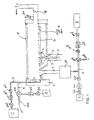
- Figure 1 illustrates a deposition apparatus adapted for delivery of sequential pulses of two different reactants A and B*, one of which B* contains excited species, to a substrate.
- the apparatus has a reaction chamber 10 with substrate 5 positioned on holder 15 which is optionally heated.
- the substrate holder can be heated resistively, inductively or by use of infrared lamps, as is known in the art.
- Gases flow into the reactor through one or more gas inlets 4 at the injector flange 6. Residual gases, after passage over the substrate are removed through an exhaust conduit 12 provided with a throttle valve 14 and a pressure measurement and control 14A.
- the reactor chamber illustrated is a radiantly heated, horizontal flow cold wall reactor, typically made of quartz, and having a divider plate 16 substantially aligned with the top surface of the substrate holder and separating the reaction chamber into upper and lower portions.
- the divider plate provides a substantially constant cross-section in the reaction area, thus, preventing recirculation cells.
- a bottom purge 17 is provided in order to prevent reactants from reaching the bottom of the reaction chamber.
- a generator of excited species 20 is provided remotely and upstream from the reaction area, and preferably upstream from the chamber 10. Most generally this generator couples an energy source into a flow of a precursor molecule (or mixture to molecules) to generate excited species.
- the generator 20 couples microwave energy from a magnetion to a gas line 8, so that the gas in inlet 7 contains excited species.
- Alternative generators suitable for use in this apparatus couple thermal energy or visable UV or IR radiation into a precursor.
- An exemplary microwave radical generator suitable for use in this invention is Rapid Reactive Radicals Technology, R 3 T, Kunststoff, Germany, model number TWR850.
- Precursors B are introduced into the excited species generator, illustrated as a microwave plasma generator, through gas line 8.
- a source of second reactant (A) is provided in gas line 9.
- Each gas line is provided with separate mass flow controls (MFC) (21 a, b and c) to allow selection of relative amounts of carrier, reactant and excited species B* introduced into the reaction chamber.
- Shut off valves (22a, b, c) to completely stop the flow of gas are provided in lines 11, 9 and 8.
- C is a carrier gas (e.g., typically N 2 or Ar)
- B is the precursor to the excited species (e.g., N 2 , H 2 , NH 3 , O 2 )
- A is a second reactant gas.
- Reactant A line 9 is provided with a dump circuit 30a which is in selective communication with line 9 via two-way valve 27a.
- Precursor B line 8 is optionally provided with a similar dump circuit 30b, two-way valve 27b and inert carrier gas circuit D (22d, 21d), analogous to the circuit for C.
- no valves are provided in conduit 7 extending from the generator of excited species to the reaction chamber to minimize decay of excited species during transport to the reaction area.
- the tube 7 is wide and short (approximately 2 cm in diameter x 15 cm long) to minimize wall losses of radicals.
- excited species can be introduced in the main carrier gas stream 4, just before it enters in the reactor.
- a unprocessed wafer is positioned on the holder in the reaction chamber, as is well known in the art.
- a main carrier gas C flow (13) is established into the reaction chamber (10) through MFC 21 c, valve 22c and the injector flange (6) on the inlet side of the reaction chamber.
- a flow of about 50 slm is used. The preferred gas flow is dependent on the design of the chamber and can be optimized without due experimentation.
- the pressure in the reaction chamber is preferably set at 0.5 to 100 Torr, and preferably 1-20 Torr, and more preferably 2-10 Torr, with conventional techniques using, for example, throttle valves (e.g., 14) and dry pumps (as known in the art, but not shown in Fig. 1 ).
- the temperature of the holder (susceptor) and substrate is controlled at a desired value by heating and thermocouple control, as is well known in the art. The optimum temperature is highly dependent on the reactants used. For the exemplary reactions discussed below, the temperature is typically in the range of about 200°C-500°C.
- a flow of reactant A is established at a desired flow rate (typically, ⁇ 1 slm, dependent upon the exact process chemistry) set by MFC 21 a through valve 27a which is initially set to flow into dump circuit 30a.
- a flow of precursor gas B is established at a desired flow rate (typically a few slm, also dependent upon the exact process chemistry) set by MFC 21 b through radical generator 20 via valve 22B.
- Flow through the generator of excited species may be a mixture of a precursor B in a carrier gas established by components D, 27d, 21 d.
- precursor gas B can be a mixture of a carrier gas and a precursor gas.
- both carrier gas C and precursor gas B are nitrogen. In that case, the dump circuit 30b, and carrier gas supply D are not needed.
- valve 27a is switched from the dump circuit to the reactor inlet for a predetermined time (t A , typically ranging from a fraction of a second to several seconds) and then switched back to the dump circuit providing a concentration pulse of reactant A into the flow of carrier gas C.
- t A a predetermined time
- t s 1 the radical generator is turned on to provide excited species B*, e.g. radicals, into the reaction chamber.
- the radical generator is kept on for a predetermined time (t B typically ranging from a fraction of a second to several seconds) and switched off to provide a pulse of excited species B*.
- the cycle of A and B* pulses is repeated, until a desired layer thickness is achieved.
- t s 2 can be different from t s 1 .
- the microwave power used is generally on the order of 100W - 5kw, and more preferably, is in the range of 500W - 2kw.
- the gas flow is almost constant, as B and C are flowing continuously and A ⁇ C, and B* ⁇ B*.
- the delay times are adjusted to avoid undesirable levels of gas phase reaction and undesirable levels of uncontrolled reaction on the substrate surface.
- Undesirable levels of gas phase and uncontrolled surface reactions are those levels of reaction that result in unacceptable defects in the layers formed on the substrate. Such defects can render the processed substrate or wafer unuseable.
- Time scheduling of pulses of reactants can readily be determined for a given reaction system and reactants by routine experimentation, as will be understood in view of the present disclosure, and is further discussed below with reference to Figs. 3A-C .
- the delay times between pulses of reactants may be different and may change during processing if desired.
- the apparatus can be provided with microprocessor and/or computer control for the automation of valves and for switching the generator of excited species on and off to provide desired timed pulses of reactants.
- microprocessor and/or computer control for the automation of valves and for switching the generator of excited species on and off to provide desired timed pulses of reactants.
- Such controls are known in the art and can be readily provided for a given apparatus.
- the apparatus has a gas inlet system having one or more gas inlets into the reaction chamber which allow establishment of carrier gas flow into the reaction chamber and into contact with a substrate surface in the chamber.
- the gas inlet system also allows introduction of one or more reactants including at least one reactant comprising excited species into the carrier gas flow which carries the reactants into contact with the substrate surface.
- Carrier gas flow is exhausted from the reaction chamber through a vacuum pump exhaust.
- the gas inlet system can have valves for generating concentration pulses of reactants.
- excited species can be generated remotely from the reaction chamber. Excited species can also be generated in situ in the reaction chamber, as is known in the art.
- the gas inlet system provides a separate conduit for introducing excited species into the carrier gas flow.
- the excited species can also be introduced into the carrier gas flow just before it enters the chamber. In this case, more losses of radicals are possible, but still enough radicals can be present to complete the reaction.
- the invention is illustrated with a horizontal flow, cold wall reactor having a constant cross-section reaction area, other horizontal designs, such as hot wall reactors, can also be employed in the methods of this invention.
- the invention can be readily adapted for use with vertical batch reaction chambers and furnaces, such as those described in U.S. patents 5,294,572 , 5,336,325 and 5,662,470 .
- the invention can also be readily adapted for use in reaction chambers in which gas flow is delivered perpendicular (rather than parallel) to the substrate surface, for example through an inlet positioned above the substrate surface, such as a shower head design. In each case, care is taken in reaction chamber design to avoid recirculation of reactants.
- Recirculation greatly enhances the residence time of reactive species which can lead to undesired gas phase reactions.
- Undesired gas phase reactions can lead to particle formation in the reaction chamber decreasing the quality of the layers formed on the substrate.
- Recirculation can be especially harmful when it occurs upstream from the wafer as then it affects the deposition process. Care must also be taken to operate the excited species as close as practically possible to the chamber to assure sufficient survival of radicals.
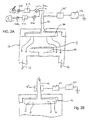
- FIG. 2A illustrates an alternate reaction chamber 10 in which excited species are formed in the reaction chamber.
- a showerhead inlet 40 is provided through which carrier flow and reactant gas pulses are established.
- a plasma can be generated by application of RF power electrically connected to the showerhead using an RF generator 42 coupled to an RF matching network, as is well-known in the art.
- Gas line 41 directs gases from gas manifolds into the showerhead inlet.
- a source of carrier gas C with valves and mass flow controller as in the apparatus of Fig. 1 , provides carrier gas flow into the chamber passing in contact with a substrate or wafer (5) on optionally heated holder 15 to exit through exhaust lines 12.
- a source of reactant A with valves, mass flow controller and dump circuit 30A, as in Fig.
- A provides concentration pulses of A into carrier gas C by timed operation of valve 27a. Pulses of A are alternated with pulses of RF power to generate alternate pulses of A and excited C* species. In this case, layers are formed by reaction of excited C* species with deposited A reactant. The pulses of A and C* are separated in time and space, as discussed above and in Figs. 3A - 3C below, to avoid an undesired level of gas phase or uncontrolled surface reactions.
- C can, for example, be nitrogen carrier gas and C* can be excited nitrogen species.
- Plasmas may also be generated in the reaction chamber using RF coils as is known in the art. RF power can be modulated as is well-known in the art to provide concentration pulse of excited species.
- An alternate means for generating a plasma employing a showerhead -type inlet is disclosed in U.S. patent 5,134,965 , which is incorporated by reference herein.
- FIG. 2B illustrates an alternative reactor design with remote plasma generation of excited species employing a showerhead inlet 40.
- An RF cavity or coil 47 is provided in the inlet line 41.
- RF power is applied from RF generator 42 through RF matching network 45 to generate a plasma in the inlet line 41.
- Excited species are formed in the inlet by pulsing the RF power on and off. Concentration pulses of excited species are carried into the reaction chamber in the carrier gas flow.
- the operation of RF generators and RF matching circuits are well-known in the art.
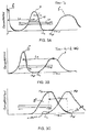
- Figures 3A and 3B schematically illustrate, in one dimension (x), progress of gas pulses traversing the reaction chamber in graphs of reactant concentration as a function of flow distance through the reaction chamber.
- Fig. 3A is at time t 0 , just as a pulse of reactant B* enters the reaction chamber (by, e.g., switching on the radical generator).
- an earlier pulse of A has traversed a distance equal to L S (the distance traversed in delay time t S between pulses of different reactant).
- L S the distance traversed in delay time t S between pulses of different reactant
- L D is the characteristic diffusion length, a measure of the broadening of the reactant pulse as a function of time due to gas diffusion
- L D 2 ⁇ Dt
- D is the diffusion coefficient of the reactant gas in the carrier
- t is the residence time
- t L R /D.
- Fig. 3B illustrates the B* pulse and A pulse at time t 0 + 1/2(L R /v). As indicated in the these figures, pulses broaden due to diffusion of reactants when the pulses traverse the reaction chamber. Pulses illustrated in Fig. 3B are sufficiently separated in distance, despite pulse broadening, to avoid interaction and reaction of reactants in different pulses.
- the delay t s between pulses is preferably sufficiently long to minimize overlap of reactant gas pulses in the reactor chamber and minimize gas phase or uncontrolled surface reactions. Significant gas phase reactions or uncontrolled reactions on the surface are avoided when L D ⁇ L S , e.g., preferably where L s is at least about 5 - 10 times L D . It should be noted that short cycles are desirable to maximize the throughput of the reactor. The desire to minimize pulse overlap is a trade-off with increased throughput.
- the delay time (t s ) between pulses e.g., the time between shutting of one reactant and admitting another reactant
- the delay time exceeds one second only at the lowest flow and highest pressure.
- reactant pulse sequences can follow each other in quite rapid succession, typically one every second, enabling a high layer growth rate. It should be noted that conditions do exist where L S >>L R . Essentially this implies that one reactant is fully purged from the reactor before the other reactant is introduced.
- Fig. 3B illustrates a pulse time scheme in which the time between pulses is sufficiently long that adjacent pulses of reactants do not overlap as they broaden and traverse the reaction chamber.
- the leading edge (LE B* ) of one pulse does not overlap the trailing edge (TE A ) of the preceding pulse.
- Significant gas phase reactions are avoided when L D is smaller (preferably 5-10 times smaller) than the distance between the trailing and leading edges of the pulses.
- Fig. 3C illustrates an embodiment where some overlap of reactant pulses is allowed. The amount of overlap illustrated in the figure typically does not result in levels of gas phase reaction or uncontrolled surface reaction that are high enough to detrimentally affect the quality of the layers formed on the substrate or wafer.
- Reactant pulse overlap can be characterized in terms of the relative concentration of the reactants at a given point in time, space or both during flow through the reactor. A preferred maximum overlap is defined as follows.
- the concentration of reactant B* at that same point is less than about 10% of the maximum concentration of B* (M B ) and at any point in time or space where the concentration of reactant B* is at its maximum (M B ), the concentration of reactant A at that same point is less than about 10% of the maximum concentration of A (M A ).
- Delay times selected to meet this maximum overlap criterium typically provide sufficiently clean layer deposition and decreased process times. In certain cases where more reactive chemistries are employed for layer deposition, the maximum overlap should be decreased to avoid undesired reactions which can affect layer quality. In such cases, the maximum concentrations of reactants A and B* at the maximum concentrations of B* and A, respectively, is 1 % or less.
- the pulse reactant system is operated under conditions that minimize diffusion, i.e., at high flow velocity.
- Delay times t S between pulse of gas are selected as described above to avoid or minimize undesired gas phase reaction between reactants and undesired uncontrolled surface reactions and to minimize processing time.
- the preferred carrier gas or gases used are nonreactive with any reactants that are to be used in a given process and also nonreactive with the substrate surface. Examples are N 2 , H 2 , noble gases and mixtures of these, the choice of which depends upon the process choice or precursors and exposed layers.
- Reactant gases include pure reactant gases, a mixture of reactants, excited species (e.g., radicals) or mixtures of excited neutrals and mixtures of excited neutrals with diluent or carrier gas. Reactants are typically introduced into the reaction chamber in a carrier gas. Reactants are in the vapor phase when introduced into the reaction chamber.
- one monolayer or less is typically grown (on the order of about 0.03 - 0.3 nm/ layer).
- Practical films useful in semiconductor applications ange in thickness from about 1 to about 50 nm. Processing times in a single wafer processing apparatus for practical films will require about 6-600 s for the illustrated reactor.
- the process cycle of layer deposition has been exemplified with sequential pulses of two reactants, one of which contains excited species.
- the method of this invention can be employed in formation of complex layers requiring more than two reactants (including reactants containing excited or activated species or radicals).
- the schedule or order of multiple reactant pulses employed in this invention can be sequential or readily adapted to any order of reactant pulsing for a wide variety of deposition or layering processes.
- the method of this invention has been exemplified with sequential pulses of reactant separated by a selected delay time (t s ) and of selected pulse duration (t A and t B ).
- the delay time between pulses of reactants can be varied over the course of multiple cycles, so long as the delay time used is sufficient to avoid an undesirable level of gas phase or uncontrolled surface reaction among reactants.
- the pulse duration of the different reactants may be the same or different and will preferably be selected to achieve a desired level of surface reaction.
- the pulse duration of the same reactants over the course of multiple cycles of layer deposition may be the same or different and will also preferably be selected to achieve a desired level of surface reaction.
- the reactant pulse schemes of Figs. 3A-C illustrate multiple pulses carried in a single flow of carrier gas, such as illustrated in the apparatus of Fig. 1 or Fig. 2 .
- sequential pulses of reactants can be delivered to a reaction area containing one or more substrates in separate carrier gas flows.
- Radicals or excited species useful in processing of substrates include, among others, active nitrogen (N*, N 2 *, N 2 + or mixtures thereof) generated by microwave discharge of nitrogen, oxygen radicals generated by microwave discharge of oxygen, radicals or reactive species generated by photolysis or thermal decomposition.
- Plasmas for radical generation can be generated by microwave or RF energy, as is well-known in the art. Radicals or excited species tend to recombine or decay into the non-excited state during transport to the reaction area through gas phase reactions and on the walls of conduits. Therefore, it is beneficial to install the radical generator as close as practical to the reaction area on the wafer surface. Further, the pressures during transport of the excited species cannot be too high. Successful generation and transport of radicals has been demonstrated at pressures up to about 50 torr in N 2 . Preferably the pressure in the apparatus of this invention is kept at about 5-10 torr.
- Excited neutrals can include radicals, and atoms and molecules in excited electronic states. Excited neutrals can be generated in plasmas sustained by RF or microwave energy. Alternatively, they can be generated by irradiation of precursor neutral species at selected wavelengths including ultra-violet (U.V.), visible and infra-red (IR) wavelengths to decompose neutrals forming radicals and or excited states. Excited neutrals, particularly radicals, can also be formed by thermal decomposition of precursors.
- U.V. ultra-violet
- IR infra-red
- the apparatus is preferably implemented with a microwave radical, excited neutrals generator which may be remote from the reactor chamber or within the reaction chamber.
- pressures are selected to be sufficiently high to facilitate ignition of a plasma as well as to limit diffusion of reactant pulses into each other to avoid undesired reactions. Pressures are also selected to be sufficiently low to avoid substantial decay of excited species or recombination of radicals so that practical levels of excited species reach the reaction area. Reactor pressures ranging from about 0.5 up to 10-20 Torr are preferred.
- a preferred microwave plasma source which provides high efficiency at these relatively low reactant pressures is described in Steinhardt et al. U.S. patent 5,489,362 , and is commercially available from R 3 T, as noted above.
- the apparatus can be used to produce silicon nitride layers on silicon wafers.
- reactant A is SiH 4 using nitrogen as the carrier gas and the substrate is heated to about 300- 550°C.
- B* is active nitrogen generated by passing nitrogen through a microwave radical generator. Repeated sequential pulses of SiH 4 and active nitrogen grows a SiN layer of desired thickness.
- the apparatus can be employed in the growth of layers by selective adsorption of a reactant.
- a reactant for example, under certain conditions metal organic precursors or SiH 4 can be made to preferentially adsorb onto Si and not onto SiO 2 or SiN 4 . Exposure of the selectively adsorbed species on Si to radicals effectively completes reaction only on Si. Thus, a layer is grown only on the area of Si. Similar adsorption selectivity of reactants and selective layer growth can be achieved on metal areas (e.g., Cu or Al) with respect to dielectrics.
- metal organic precursors or SiH 4 can be made to preferentially adsorb onto Si and not onto SiO 2 or SiN 4 . Exposure of the selectively adsorbed species on Si to radicals effectively completes reaction only on Si. Thus, a layer is grown only on the area of Si. Similar adsorption selectivity of reactants and selective layer growth can be achieved on metal areas (e.g., Cu or Al) with respect to dielectrics.
- the pulsed gas flow apparatus of this invention is preferably implemented in a horizontal flow reactor in a reactor system as described, for example, in Crabb et al. U.S. patents 4,828,224 , 5, 156,521 , 5,092,728 , and 5,435,682 .
- a variety of substrates and wafers of different sizes, shapes and materials can be processed by the method of this invention.
- Substrates are positioned in a substrate holder (a susceptor) that is typically heated.
- a variety of substrate holders are known in the art. Multiple substrates can be processed simultaneously, for example, by stacking the wafers in a boat, positioning wafers laterally apart on a single susceptor or by having multiple susceptors for holding one or more wafers in a reaction chamber.
Landscapes
- Chemical & Material Sciences (AREA)
- Engineering & Computer Science (AREA)
- Materials Engineering (AREA)
- Organic Chemistry (AREA)
- Metallurgy (AREA)
- Chemical Kinetics & Catalysis (AREA)
- General Chemical & Material Sciences (AREA)
- Mechanical Engineering (AREA)
- Physics & Mathematics (AREA)
- Plasma & Fusion (AREA)
- Electromagnetism (AREA)
- Crystallography & Structural Chemistry (AREA)
- Analytical Chemistry (AREA)
- Inorganic Chemistry (AREA)
- Chemical Vapour Deposition (AREA)
Applications Claiming Priority (3)
| Application Number | Priority Date | Filing Date | Title |
|---|---|---|---|
| US392371 | 1999-09-08 | ||
| US09/392,371 US6511539B1 (en) | 1999-09-08 | 1999-09-08 | Apparatus and method for growth of a thin film |
| PCT/US2000/024586 WO2001017692A1 (en) | 1999-09-08 | 2000-09-08 | Improved apparatus and method for growth of a thin film |
Publications (3)
| Publication Number | Publication Date |
|---|---|
| EP1216106A1 EP1216106A1 (en) | 2002-06-26 |
| EP1216106A4 EP1216106A4 (en) | 2005-09-28 |
| EP1216106B1 true EP1216106B1 (en) | 2014-05-21 |
Family
ID=23550311
Family Applications (1)
| Application Number | Title | Priority Date | Filing Date |
|---|---|---|---|
| EP00963326.4A Expired - Lifetime EP1216106B1 (en) | 1999-09-08 | 2000-09-08 | Improved apparatus and method for growth of a thin film |
Country Status (6)
| Country | Link |
|---|---|
| US (4) | US6511539B1 (https=) |
| EP (1) | EP1216106B1 (https=) |
| JP (1) | JP4994551B2 (https=) |
| KR (1) | KR100853702B1 (https=) |
| TW (1) | TW527224B (https=) |
| WO (1) | WO2001017692A1 (https=) |
Families Citing this family (755)
| Publication number | Priority date | Publication date | Assignee | Title |
|---|---|---|---|---|
| US7393561B2 (en) * | 1997-08-11 | 2008-07-01 | Applied Materials, Inc. | Method and apparatus for layer by layer deposition of thin films |
| US6974766B1 (en) * | 1998-10-01 | 2005-12-13 | Applied Materials, Inc. | In situ deposition of a low κ dielectric layer, barrier layer, etch stop, and anti-reflective coating for damascene application |
| US6511539B1 (en) * | 1999-09-08 | 2003-01-28 | Asm America, Inc. | Apparatus and method for growth of a thin film |
| US6319766B1 (en) | 2000-02-22 | 2001-11-20 | Applied Materials, Inc. | Method of tantalum nitride deposition by tantalum oxide densification |
| US7494927B2 (en) * | 2000-05-15 | 2009-02-24 | Asm International N.V. | Method of growing electrical conductors |
| JP3687651B2 (ja) * | 2000-06-08 | 2005-08-24 | ジニテック インク. | 薄膜形成方法 |
| US6620723B1 (en) * | 2000-06-27 | 2003-09-16 | Applied Materials, Inc. | Formation of boride barrier layers using chemisorption techniques |
| US7101795B1 (en) | 2000-06-28 | 2006-09-05 | Applied Materials, Inc. | Method and apparatus for depositing refractory metal layers employing sequential deposition techniques to form a nucleation layer |
| US7405158B2 (en) * | 2000-06-28 | 2008-07-29 | Applied Materials, Inc. | Methods for depositing tungsten layers employing atomic layer deposition techniques |
| US6551929B1 (en) * | 2000-06-28 | 2003-04-22 | Applied Materials, Inc. | Bifurcated deposition process for depositing refractory metal layers employing atomic layer deposition and chemical vapor deposition techniques |
| US6936538B2 (en) * | 2001-07-16 | 2005-08-30 | Applied Materials, Inc. | Method and apparatus for depositing tungsten after surface treatment to improve film characteristics |
| US20020036780A1 (en) * | 2000-09-27 | 2002-03-28 | Hiroaki Nakamura | Image processing apparatus |
| US9255329B2 (en) * | 2000-12-06 | 2016-02-09 | Novellus Systems, Inc. | Modulated ion-induced atomic layer deposition (MII-ALD) |
| US6998579B2 (en) | 2000-12-29 | 2006-02-14 | Applied Materials, Inc. | Chamber for uniform substrate heating |
| US6825447B2 (en) | 2000-12-29 | 2004-11-30 | Applied Materials, Inc. | Apparatus and method for uniform substrate heating and contaminate collection |
| US6765178B2 (en) | 2000-12-29 | 2004-07-20 | Applied Materials, Inc. | Chamber for uniform substrate heating |
| US6951804B2 (en) * | 2001-02-02 | 2005-10-04 | Applied Materials, Inc. | Formation of a tantalum-nitride layer |
| KR101027485B1 (ko) * | 2001-02-12 | 2011-04-06 | 에이에스엠 아메리카, 인코포레이티드 | 반도체 박막 증착을 위한 개선된 공정 |
| US6613656B2 (en) * | 2001-02-13 | 2003-09-02 | Micron Technology, Inc. | Sequential pulse deposition |
| US6660126B2 (en) | 2001-03-02 | 2003-12-09 | Applied Materials, Inc. | Lid assembly for a processing system to facilitate sequential deposition techniques |
| WO2002071463A1 (en) * | 2001-03-02 | 2002-09-12 | Tokyo Electron Limited | Shower head gas injection apparatus with secondary high pressure pulsed gas injection |
| US6878206B2 (en) | 2001-07-16 | 2005-04-12 | Applied Materials, Inc. | Lid assembly for a processing system to facilitate sequential deposition techniques |
| US6627268B1 (en) * | 2001-05-03 | 2003-09-30 | Novellus Systems, Inc. | Sequential ion, UV, and electron induced chemical vapor deposition |
| US6596643B2 (en) * | 2001-05-07 | 2003-07-22 | Applied Materials, Inc. | CVD TiSiN barrier for copper integration |
| JP2002339071A (ja) * | 2001-05-18 | 2002-11-27 | L'air Liquide Sa Pour L'etude & L'exploitation Des Procede S Georges Claude | Alcvdシステムにおける処理ガス供給機構 |
| JP2002343790A (ja) * | 2001-05-21 | 2002-11-29 | Nec Corp | 金属化合物薄膜の気相堆積方法及び半導体装置の製造方法 |
| US7037574B2 (en) | 2001-05-23 | 2006-05-02 | Veeco Instruments, Inc. | Atomic layer deposition for fabricating thin films |
| US6828218B2 (en) * | 2001-05-31 | 2004-12-07 | Samsung Electronics Co., Ltd. | Method of forming a thin film using atomic layer deposition |
| US6849545B2 (en) * | 2001-06-20 | 2005-02-01 | Applied Materials, Inc. | System and method to form a composite film stack utilizing sequential deposition techniques |
| US20030198754A1 (en) * | 2001-07-16 | 2003-10-23 | Ming Xi | Aluminum oxide chamber and process |
| KR100427996B1 (ko) * | 2001-07-19 | 2004-04-28 | 주식회사 아이피에스 | 박막증착용 반응용기 및 그를 이용한 박막증착방법 |
| US20060201428A1 (en) * | 2001-07-19 | 2006-09-14 | Park Young H | Shower head and method of fabricating the same |
| JP2005504885A (ja) | 2001-07-25 | 2005-02-17 | アプライド マテリアルズ インコーポレイテッド | 新規なスパッタ堆積方法を使用したバリア形成 |
| US20090004850A1 (en) * | 2001-07-25 | 2009-01-01 | Seshadri Ganguli | Process for forming cobalt and cobalt silicide materials in tungsten contact applications |
| US20080268635A1 (en) * | 2001-07-25 | 2008-10-30 | Sang-Ho Yu | Process for forming cobalt and cobalt silicide materials in copper contact applications |
| US9051641B2 (en) | 2001-07-25 | 2015-06-09 | Applied Materials, Inc. | Cobalt deposition on barrier surfaces |
| US20030029715A1 (en) * | 2001-07-25 | 2003-02-13 | Applied Materials, Inc. | An Apparatus For Annealing Substrates In Physical Vapor Deposition Systems |
| US8110489B2 (en) * | 2001-07-25 | 2012-02-07 | Applied Materials, Inc. | Process for forming cobalt-containing materials |
| US7085616B2 (en) * | 2001-07-27 | 2006-08-01 | Applied Materials, Inc. | Atomic layer deposition apparatus |
| WO2003023835A1 (en) * | 2001-08-06 | 2003-03-20 | Genitech Co., Ltd. | Plasma enhanced atomic layer deposition (peald) equipment and method of forming a conducting thin film using the same thereof |
| US6820570B2 (en) | 2001-08-15 | 2004-11-23 | Nobel Biocare Services Ag | Atomic layer deposition reactor |
| WO2003021002A1 (en) * | 2001-08-29 | 2003-03-13 | Tokyo Electron Limited | Apparatus and method for plasma processing |
| US6718126B2 (en) * | 2001-09-14 | 2004-04-06 | Applied Materials, Inc. | Apparatus and method for vaporizing solid precursor for CVD or atomic layer deposition |
| US20030059538A1 (en) * | 2001-09-26 | 2003-03-27 | Applied Materials, Inc. | Integration of barrier layer and seed layer |
| US7049226B2 (en) * | 2001-09-26 | 2006-05-23 | Applied Materials, Inc. | Integration of ALD tantalum nitride for copper metallization |
| US6936906B2 (en) * | 2001-09-26 | 2005-08-30 | Applied Materials, Inc. | Integration of barrier layer and seed layer |
| US6916398B2 (en) | 2001-10-26 | 2005-07-12 | Applied Materials, Inc. | Gas delivery apparatus and method for atomic layer deposition |
| US7780785B2 (en) | 2001-10-26 | 2010-08-24 | Applied Materials, Inc. | Gas delivery apparatus for atomic layer deposition |
| KR100760291B1 (ko) * | 2001-11-08 | 2007-09-19 | 에이에스엠지니텍코리아 주식회사 | 박막 형성 방법 |
| KR100782529B1 (ko) * | 2001-11-08 | 2007-12-06 | 에이에스엠지니텍코리아 주식회사 | 증착 장치 |
| US6773507B2 (en) * | 2001-12-06 | 2004-08-10 | Applied Materials, Inc. | Apparatus and method for fast-cycle atomic layer deposition |
| US7081271B2 (en) * | 2001-12-07 | 2006-07-25 | Applied Materials, Inc. | Cyclical deposition of refractory metal silicon nitride |
| US6729824B2 (en) | 2001-12-14 | 2004-05-04 | Applied Materials, Inc. | Dual robot processing system |
| US6939801B2 (en) * | 2001-12-21 | 2005-09-06 | Applied Materials, Inc. | Selective deposition of a barrier layer on a dielectric material |
| WO2003065424A2 (en) * | 2002-01-25 | 2003-08-07 | Applied Materials, Inc. | Apparatus for cyclical deposition of thin films |
| US6866746B2 (en) * | 2002-01-26 | 2005-03-15 | Applied Materials, Inc. | Clamshell and small volume chamber with fixed substrate support |
| US6998014B2 (en) | 2002-01-26 | 2006-02-14 | Applied Materials, Inc. | Apparatus and method for plasma assisted deposition |
| US6911391B2 (en) * | 2002-01-26 | 2005-06-28 | Applied Materials, Inc. | Integration of titanium and titanium nitride layers |
| US6787185B2 (en) * | 2002-02-25 | 2004-09-07 | Micron Technology, Inc. | Deposition methods for improved delivery of metastable species |
| US6833161B2 (en) * | 2002-02-26 | 2004-12-21 | Applied Materials, Inc. | Cyclical deposition of tungsten nitride for metal oxide gate electrode |
| US6972267B2 (en) * | 2002-03-04 | 2005-12-06 | Applied Materials, Inc. | Sequential deposition of tantalum nitride using a tantalum-containing precursor and a nitrogen-containing precursor |
| US6893506B2 (en) * | 2002-03-11 | 2005-05-17 | Micron Technology, Inc. | Atomic layer deposition apparatus and method |
| US6800134B2 (en) * | 2002-03-26 | 2004-10-05 | Micron Technology, Inc. | Chemical vapor deposition methods and atomic layer deposition methods |
| US6825134B2 (en) * | 2002-03-26 | 2004-11-30 | Applied Materials, Inc. | Deposition of film layers by alternately pulsing a precursor and high frequency power in a continuous gas flow |
| US6720027B2 (en) * | 2002-04-08 | 2004-04-13 | Applied Materials, Inc. | Cyclical deposition of a variable content titanium silicon nitride layer |
| US6846516B2 (en) * | 2002-04-08 | 2005-01-25 | Applied Materials, Inc. | Multiple precursor cyclical deposition system |
| JP4695343B2 (ja) * | 2002-04-11 | 2011-06-08 | 株式会社日立国際電気 | 縦型半導体製造装置 |
| US7279432B2 (en) * | 2002-04-16 | 2007-10-09 | Applied Materials, Inc. | System and method for forming an integrated barrier layer |
| US20030235961A1 (en) * | 2002-04-17 | 2003-12-25 | Applied Materials, Inc. | Cyclical sequential deposition of multicomponent films |
| US7374617B2 (en) * | 2002-04-25 | 2008-05-20 | Micron Technology, Inc. | Atomic layer deposition methods and chemical vapor deposition methods |
| US20030215570A1 (en) * | 2002-05-16 | 2003-11-20 | Applied Materials, Inc. | Deposition of silicon nitride |
| US7041335B2 (en) * | 2002-06-04 | 2006-05-09 | Applied Materials, Inc. | Titanium tantalum nitride silicide layer |
| US6838125B2 (en) * | 2002-07-10 | 2005-01-04 | Applied Materials, Inc. | Method of film deposition using activated precursor gases |
| US20040013803A1 (en) * | 2002-07-16 | 2004-01-22 | Applied Materials, Inc. | Formation of titanium nitride films using a cyclical deposition process |
| US6955211B2 (en) | 2002-07-17 | 2005-10-18 | Applied Materials, Inc. | Method and apparatus for gas temperature control in a semiconductor processing system |
| US7186385B2 (en) | 2002-07-17 | 2007-03-06 | Applied Materials, Inc. | Apparatus for providing gas to a processing chamber |
| US7066194B2 (en) * | 2002-07-19 | 2006-06-27 | Applied Materials, Inc. | Valve design and configuration for fast delivery system |
| US6772072B2 (en) * | 2002-07-22 | 2004-08-03 | Applied Materials, Inc. | Method and apparatus for monitoring solid precursor delivery |
| US6915592B2 (en) * | 2002-07-29 | 2005-07-12 | Applied Materials, Inc. | Method and apparatus for generating gas to a processing chamber |
| US6887521B2 (en) * | 2002-08-15 | 2005-05-03 | Micron Technology, Inc. | Gas delivery system for pulsed-type deposition processes used in the manufacturing of micro-devices |
| US6995081B2 (en) * | 2002-08-28 | 2006-02-07 | Micron Technology, Inc. | Systems and methods for forming tantalum silicide layers |
| US6967159B2 (en) * | 2002-08-28 | 2005-11-22 | Micron Technology, Inc. | Systems and methods for forming refractory metal nitride layers using organic amines |
| US6794284B2 (en) * | 2002-08-28 | 2004-09-21 | Micron Technology, Inc. | Systems and methods for forming refractory metal nitride layers using disilazanes |
| JP3594947B2 (ja) * | 2002-09-19 | 2004-12-02 | 東京エレクトロン株式会社 | 絶縁膜の形成方法、半導体装置の製造方法、基板処理装置 |
| KR100467357B1 (ko) * | 2002-09-24 | 2005-01-24 | 삼성전자주식회사 | 모오스 트랜지스터 제조 방법 |
| US20040065255A1 (en) * | 2002-10-02 | 2004-04-08 | Applied Materials, Inc. | Cyclical layer deposition system |
| US6821563B2 (en) | 2002-10-02 | 2004-11-23 | Applied Materials, Inc. | Gas distribution system for cyclical layer deposition |
| US20040069227A1 (en) * | 2002-10-09 | 2004-04-15 | Applied Materials, Inc. | Processing chamber configured for uniform gas flow |
| US6905737B2 (en) * | 2002-10-11 | 2005-06-14 | Applied Materials, Inc. | Method of delivering activated species for rapid cyclical deposition |
| US7540920B2 (en) * | 2002-10-18 | 2009-06-02 | Applied Materials, Inc. | Silicon-containing layer deposition with silicon compounds |
| US7097782B2 (en) | 2002-11-12 | 2006-08-29 | Micron Technology, Inc. | Method of exposing a substrate to a surface microwave plasma, etching method, deposition method, surface microwave plasma generating apparatus, semiconductor substrate etching apparatus, semiconductor substrate deposition apparatus, and microwave plasma generating antenna assembly |
| US7022605B2 (en) | 2002-11-12 | 2006-04-04 | Micron Technology, Inc. | Atomic layer deposition methods |
| EP1420080A3 (en) * | 2002-11-14 | 2005-11-09 | Applied Materials, Inc. | Apparatus and method for hybrid chemical deposition processes |
| US20040142558A1 (en) | 2002-12-05 | 2004-07-22 | Granneman Ernst H. A. | Apparatus and method for atomic layer deposition on substrates |
| US7244683B2 (en) * | 2003-01-07 | 2007-07-17 | Applied Materials, Inc. | Integration of ALD/CVD barriers with porous low k materials |
| US7262133B2 (en) | 2003-01-07 | 2007-08-28 | Applied Materials, Inc. | Enhancement of copper line reliability using thin ALD tan film to cap the copper line |
| US6753248B1 (en) | 2003-01-27 | 2004-06-22 | Applied Materials, Inc. | Post metal barrier/adhesion film |
| US6994319B2 (en) * | 2003-01-29 | 2006-02-07 | Applied Materials, Inc. | Membrane gas valve for pulsing a gas |
| US6868859B2 (en) * | 2003-01-29 | 2005-03-22 | Applied Materials, Inc. | Rotary gas valve for pulsing a gas |
| US20040177813A1 (en) | 2003-03-12 | 2004-09-16 | Applied Materials, Inc. | Substrate support lift mechanism |
| US6955986B2 (en) | 2003-03-27 | 2005-10-18 | Asm International N.V. | Atomic layer deposition methods for forming a multi-layer adhesion-barrier layer for integrated circuits |
| US6972055B2 (en) * | 2003-03-28 | 2005-12-06 | Finens Corporation | Continuous flow deposition system |
| US7342984B1 (en) | 2003-04-03 | 2008-03-11 | Zilog, Inc. | Counting clock cycles over the duration of a first character and using a remainder value to determine when to sample a bit of a second character |
| US20040198069A1 (en) * | 2003-04-04 | 2004-10-07 | Applied Materials, Inc. | Method for hafnium nitride deposition |
| US20050070126A1 (en) * | 2003-04-21 | 2005-03-31 | Yoshihide Senzaki | System and method for forming multi-component dielectric films |
| TW200506093A (en) * | 2003-04-21 | 2005-02-16 | Aviza Tech Inc | System and method for forming multi-component films |
| US7601223B2 (en) | 2003-04-29 | 2009-10-13 | Asm International N.V. | Showerhead assembly and ALD methods |
| US7537662B2 (en) | 2003-04-29 | 2009-05-26 | Asm International N.V. | Method and apparatus for depositing thin films on a surface |
| US7211508B2 (en) | 2003-06-18 | 2007-05-01 | Applied Materials, Inc. | Atomic layer deposition of tantalum based barrier materials |
| US20050178336A1 (en) * | 2003-07-15 | 2005-08-18 | Heng Liu | Chemical vapor deposition reactor having multiple inlets |
| US20050011459A1 (en) * | 2003-07-15 | 2005-01-20 | Heng Liu | Chemical vapor deposition reactor |
| US7399388B2 (en) * | 2003-07-25 | 2008-07-15 | Applied Materials, Inc. | Sequential gas flow oxide deposition technique |
| WO2005017963A2 (en) * | 2003-08-04 | 2005-02-24 | Asm America, Inc. | Surface preparation prior to deposition on germanium |
| US7378129B2 (en) * | 2003-08-18 | 2008-05-27 | Micron Technology, Inc. | Atomic layer deposition methods of forming conductive metal nitride comprising layers |
| CN100545303C (zh) | 2003-08-20 | 2009-09-30 | 维高仪器股份有限公司 | 用于竖流型转盘式反应器的烷基挤出流 |
| US7235482B2 (en) * | 2003-09-08 | 2007-06-26 | Taiwan Semiconductor Manufacturing Company, Ltd. | Method of manufacturing a contact interconnection layer containing a metal and nitrogen by atomic layer deposition for deep sub-micron semiconductor technology |
| US7018469B2 (en) * | 2003-09-23 | 2006-03-28 | Micron Technology, Inc. | Atomic layer deposition methods of forming silicon dioxide comprising layers |
| US20050067103A1 (en) * | 2003-09-26 | 2005-03-31 | Applied Materials, Inc. | Interferometer endpoint monitoring device |
| US6867152B1 (en) | 2003-09-26 | 2005-03-15 | Novellus Systems, Inc. | Properties of a silica thin film produced by a rapid vapor deposition (RVD) process |
| US6924223B2 (en) | 2003-09-30 | 2005-08-02 | Tokyo Electron Limited | Method of forming a metal layer using an intermittent precursor gas flow process |
| US20050069641A1 (en) * | 2003-09-30 | 2005-03-31 | Tokyo Electron Limited | Method for depositing metal layers using sequential flow deposition |
| US7166528B2 (en) * | 2003-10-10 | 2007-01-23 | Applied Materials, Inc. | Methods of selective deposition of heavily doped epitaxial SiGe |
| US20050095859A1 (en) * | 2003-11-03 | 2005-05-05 | Applied Materials, Inc. | Precursor delivery system with rate control |
| US7071118B2 (en) * | 2003-11-12 | 2006-07-04 | Veeco Instruments, Inc. | Method and apparatus for fabricating a conformal thin film on a substrate |
| US20050109276A1 (en) * | 2003-11-25 | 2005-05-26 | Applied Materials, Inc. | Thermal chemical vapor deposition of silicon nitride using BTBAS bis(tertiary-butylamino silane) in a single wafer chamber |
| KR100560654B1 (ko) * | 2004-01-08 | 2006-03-16 | 삼성전자주식회사 | 질화실리콘막을 형성을 위한 질소화합물 및 이를 이용한질화실리콘 막의 형성방법 |
| KR101025323B1 (ko) * | 2004-01-13 | 2011-03-29 | 가부시키가이샤 아루박 | 에칭 장치 및 에칭 방법 |
| US20050210455A1 (en) * | 2004-03-18 | 2005-09-22 | International Business Machines Corporation | Method for generating an executable workflow code from an unstructured cyclic process model |
| US20050252449A1 (en) * | 2004-05-12 | 2005-11-17 | Nguyen Son T | Control of gas flow and delivery to suppress the formation of particles in an MOCVD/ALD system |
| US8119210B2 (en) | 2004-05-21 | 2012-02-21 | Applied Materials, Inc. | Formation of a silicon oxynitride layer on a high-k dielectric material |
| US20060153995A1 (en) * | 2004-05-21 | 2006-07-13 | Applied Materials, Inc. | Method for fabricating a dielectric stack |
| US20060019033A1 (en) * | 2004-05-21 | 2006-01-26 | Applied Materials, Inc. | Plasma treatment of hafnium-containing materials |
| US20060062917A1 (en) * | 2004-05-21 | 2006-03-23 | Shankar Muthukrishnan | Vapor deposition of hafnium silicate materials with tris(dimethylamino)silane |
| US8323754B2 (en) * | 2004-05-21 | 2012-12-04 | Applied Materials, Inc. | Stabilization of high-k dielectric materials |
| US7097878B1 (en) | 2004-06-22 | 2006-08-29 | Novellus Systems, Inc. | Mixed alkoxy precursors and methods of their use for rapid vapor deposition of SiO2 films |
| US7129189B1 (en) | 2004-06-22 | 2006-10-31 | Novellus Systems, Inc. | Aluminum phosphate incorporation in silica thin films produced by rapid surface catalyzed vapor deposition (RVD) |
| US7202185B1 (en) | 2004-06-22 | 2007-04-10 | Novellus Systems, Inc. | Silica thin films produced by rapid surface catalyzed vapor deposition (RVD) using a nucleation layer |
| US7297608B1 (en) | 2004-06-22 | 2007-11-20 | Novellus Systems, Inc. | Method for controlling properties of conformal silica nanolaminates formed by rapid vapor deposition |
| US7241686B2 (en) * | 2004-07-20 | 2007-07-10 | Applied Materials, Inc. | Atomic layer deposition of tantalum-containing materials using the tantalum precursor TAIMATA |
| US20060019032A1 (en) * | 2004-07-23 | 2006-01-26 | Yaxin Wang | Low thermal budget silicon nitride formation for advance transistor fabrication |
| DE102004040943B4 (de) * | 2004-08-24 | 2008-07-31 | Qimonda Ag | Verfahren zur selektiven Abscheidung einer Schicht mittels eines ALD-Verfahrens |
| US20060046719A1 (en) * | 2004-08-30 | 2006-03-02 | Holtschneider David J | Method and apparatus for automatic connection of communication devices |
| US8158488B2 (en) | 2004-08-31 | 2012-04-17 | Micron Technology, Inc. | Method of increasing deposition rate of silicon dioxide on a catalyst |
| US20060084283A1 (en) * | 2004-10-20 | 2006-04-20 | Paranjpe Ajit P | Low temperature sin deposition methods |
| US7790633B1 (en) | 2004-10-26 | 2010-09-07 | Novellus Systems, Inc. | Sequential deposition/anneal film densification method |
| US7148155B1 (en) | 2004-10-26 | 2006-12-12 | Novellus Systems, Inc. | Sequential deposition/anneal film densification method |
| KR100636037B1 (ko) * | 2004-11-19 | 2006-10-18 | 삼성전자주식회사 | 티타늄 질화막 형성 방법 및 이를 수행하기 위한 장치 |
| KR100636036B1 (ko) * | 2004-11-19 | 2006-10-18 | 삼성전자주식회사 | 티타늄 질화막 형성 방법 및 이를 수행하기 위한 장치 |
| US7682940B2 (en) | 2004-12-01 | 2010-03-23 | Applied Materials, Inc. | Use of Cl2 and/or HCl during silicon epitaxial film formation |
| US7560352B2 (en) * | 2004-12-01 | 2009-07-14 | Applied Materials, Inc. | Selective deposition |
| US7312128B2 (en) * | 2004-12-01 | 2007-12-25 | Applied Materials, Inc. | Selective epitaxy process with alternating gas supply |
| US7429402B2 (en) * | 2004-12-10 | 2008-09-30 | Applied Materials, Inc. | Ruthenium as an underlayer for tungsten film deposition |
| US7294583B1 (en) | 2004-12-23 | 2007-11-13 | Novellus Systems, Inc. | Methods for the use of alkoxysilanol precursors for vapor deposition of SiO2 films |
| US7482247B1 (en) | 2004-12-30 | 2009-01-27 | Novellus Systems, Inc. | Conformal nanolaminate dielectric deposition and etch bag gap fill process |
| US7223707B1 (en) | 2004-12-30 | 2007-05-29 | Novellus Systems, Inc. | Dynamic rapid vapor deposition process for conformal silica laminates |
| US7271112B1 (en) | 2004-12-30 | 2007-09-18 | Novellus Systems, Inc. | Methods for forming high density, conformal, silica nanolaminate films via pulsed deposition layer in structures of confined geometry |
| KR101332739B1 (ko) * | 2005-01-18 | 2013-11-25 | 에이에스엠 아메리카, 인코포레이티드 | 박막 성장용 반응 시스템 |
| US7235492B2 (en) * | 2005-01-31 | 2007-06-26 | Applied Materials, Inc. | Low temperature etchant for treatment of silicon-containing surfaces |
| US20060177601A1 (en) * | 2005-02-10 | 2006-08-10 | Hyung-Sang Park | Method of forming a ruthenium thin film using a plasma enhanced atomic layer deposition apparatus and the method thereof |
| JP2008532271A (ja) * | 2005-02-22 | 2008-08-14 | エーエスエム アメリカ インコーポレイテッド | 原子層堆積のための表面のプラズマ前処理 |
| US7135418B1 (en) | 2005-03-09 | 2006-11-14 | Novellus Systems, Inc. | Optimal operation of conformal silica deposition reactors |
| US7109129B1 (en) | 2005-03-09 | 2006-09-19 | Novellus Systems, Inc. | Optimal operation of conformal silica deposition reactors |
| US8025922B2 (en) * | 2005-03-15 | 2011-09-27 | Asm International N.V. | Enhanced deposition of noble metals |
| US7608549B2 (en) * | 2005-03-15 | 2009-10-27 | Asm America, Inc. | Method of forming non-conformal layers |
| US7666773B2 (en) | 2005-03-15 | 2010-02-23 | Asm International N.V. | Selective deposition of noble metal thin films |
| US20060216548A1 (en) * | 2005-03-22 | 2006-09-28 | Ming Mao | Nanolaminate thin films and method for forming the same using atomic layer deposition |
| WO2006106764A1 (ja) * | 2005-03-30 | 2006-10-12 | Matsushita Electric Industrial Co., Ltd. | 伝送線路 |
| KR100628995B1 (ko) | 2005-03-30 | 2006-09-27 | 이선영 | 반도체 웨이퍼가공용 수소가스 자동처리시스템 |
| US7396415B2 (en) * | 2005-06-02 | 2008-07-08 | Asm America, Inc. | Apparatus and methods for isolating chemical vapor reactions at a substrate surface |
| US20060272577A1 (en) * | 2005-06-03 | 2006-12-07 | Ming Mao | Method and apparatus for decreasing deposition time of a thin film |
| US7651955B2 (en) * | 2005-06-21 | 2010-01-26 | Applied Materials, Inc. | Method for forming silicon-containing materials during a photoexcitation deposition process |
| US20060286774A1 (en) * | 2005-06-21 | 2006-12-21 | Applied Materials. Inc. | Method for forming silicon-containing materials during a photoexcitation deposition process |
| US7648927B2 (en) | 2005-06-21 | 2010-01-19 | Applied Materials, Inc. | Method for forming silicon-containing materials during a photoexcitation deposition process |
| US20070014919A1 (en) * | 2005-07-15 | 2007-01-18 | Jani Hamalainen | Atomic layer deposition of noble metal oxides |
| US20070020890A1 (en) * | 2005-07-19 | 2007-01-25 | Applied Materials, Inc. | Method and apparatus for semiconductor processing |
| US20070049043A1 (en) * | 2005-08-23 | 2007-03-01 | Applied Materials, Inc. | Nitrogen profile engineering in HI-K nitridation for device performance enhancement and reliability improvement |
| US7402534B2 (en) * | 2005-08-26 | 2008-07-22 | Applied Materials, Inc. | Pretreatment processes within a batch ALD reactor |
| US7521356B2 (en) * | 2005-09-01 | 2009-04-21 | Micron Technology, Inc. | Atomic layer deposition systems and methods including silicon-containing tantalum precursor compounds |
| US20070065576A1 (en) * | 2005-09-09 | 2007-03-22 | Vikram Singh | Technique for atomic layer deposition |
| US20070065578A1 (en) * | 2005-09-21 | 2007-03-22 | Applied Materials, Inc. | Treatment processes for a batch ALD reactor |
| US20070082507A1 (en) * | 2005-10-06 | 2007-04-12 | Applied Materials, Inc. | Method and apparatus for the low temperature deposition of doped silicon nitride films |
| US7464917B2 (en) * | 2005-10-07 | 2008-12-16 | Appiled Materials, Inc. | Ampoule splash guard apparatus |
| US8993055B2 (en) | 2005-10-27 | 2015-03-31 | Asm International N.V. | Enhanced thin film deposition |
| US20070099422A1 (en) * | 2005-10-28 | 2007-05-03 | Kapila Wijekoon | Process for electroless copper deposition |
| KR101019293B1 (ko) * | 2005-11-04 | 2011-03-07 | 어플라이드 머티어리얼스, 인코포레이티드 | 플라즈마-강화 원자층 증착 장치 및 방법 |
| US7589028B1 (en) | 2005-11-15 | 2009-09-15 | Novellus Systems, Inc. | Hydroxyl bond removal and film densification method for oxide films using microwave post treatment |
| US7658802B2 (en) * | 2005-11-22 | 2010-02-09 | Applied Materials, Inc. | Apparatus and a method for cleaning a dielectric film |
| US7491653B1 (en) | 2005-12-23 | 2009-02-17 | Novellus Systems, Inc. | Metal-free catalysts for pulsed deposition layer process for conformal silica laminates |
| KR101379015B1 (ko) | 2006-02-15 | 2014-03-28 | 한국에이에스엠지니텍 주식회사 | 플라즈마 원자층 증착법을 이용한 루테늄 막 증착 방법 및고밀도 루테늄 층 |
| US7964514B2 (en) * | 2006-03-02 | 2011-06-21 | Applied Materials, Inc. | Multiple nitrogen plasma treatments for thin SiON dielectrics |
| US20070215036A1 (en) * | 2006-03-15 | 2007-09-20 | Hyung-Sang Park | Method and apparatus of time and space co-divided atomic layer deposition |
| US20070218702A1 (en) * | 2006-03-15 | 2007-09-20 | Asm Japan K.K. | Semiconductor-processing apparatus with rotating susceptor |
| WO2007112058A2 (en) * | 2006-03-24 | 2007-10-04 | Applied Materials, Inc. | Carbon precursors for use during silicon epitaxial firm formation |
| US7737035B1 (en) | 2006-03-31 | 2010-06-15 | Novellus Systems, Inc. | Dual seal deposition process chamber and process |
| US7674337B2 (en) * | 2006-04-07 | 2010-03-09 | Applied Materials, Inc. | Gas manifolds for use during epitaxial film formation |
| US20070252299A1 (en) * | 2006-04-27 | 2007-11-01 | Applied Materials, Inc. | Synchronization of precursor pulsing and wafer rotation |
| US7537804B2 (en) * | 2006-04-28 | 2009-05-26 | Micron Technology, Inc. | ALD methods in which two or more different precursors are utilized with one or more reactants to form materials over substrates |
| US7288463B1 (en) | 2006-04-28 | 2007-10-30 | Novellus Systems, Inc. | Pulsed deposition layer gap fill with expansion material |
| US7798096B2 (en) * | 2006-05-05 | 2010-09-21 | Applied Materials, Inc. | Plasma, UV and ion/neutral assisted ALD or CVD in a batch tool |
| US20070259111A1 (en) * | 2006-05-05 | 2007-11-08 | Singh Kaushal K | Method and apparatus for photo-excitation of chemicals for atomic layer deposition of dielectric film |
| US7625820B1 (en) | 2006-06-21 | 2009-12-01 | Novellus Systems, Inc. | Method of selective coverage of high aspect ratio structures with a conformal film |
| US7501355B2 (en) * | 2006-06-29 | 2009-03-10 | Applied Materials, Inc. | Decreasing the etch rate of silicon nitride by carbon addition |
| WO2008005892A2 (en) * | 2006-06-30 | 2008-01-10 | Applied Materials, Inc. | Nanocrystal formation |
| US7795160B2 (en) * | 2006-07-21 | 2010-09-14 | Asm America Inc. | ALD of metal silicate films |
| WO2008016836A2 (en) * | 2006-07-29 | 2008-02-07 | Lotus Applied Technology, Llc | Radical-enhanced atomic layer deposition system and method |
| CN101496153A (zh) * | 2006-07-31 | 2009-07-29 | 应用材料股份有限公司 | 形成含碳外延硅层的方法 |
| WO2008033186A1 (en) * | 2006-07-31 | 2008-03-20 | Applied Materials, Inc. | Methods of controlling morphology during epitaxial layer formation |
| US20080038486A1 (en) * | 2006-08-03 | 2008-02-14 | Helmuth Treichel | Radical Assisted Batch Film Deposition |
| US7435484B2 (en) * | 2006-09-01 | 2008-10-14 | Asm Japan K.K. | Ruthenium thin film-formed structure |
| US8053372B1 (en) | 2006-09-12 | 2011-11-08 | Novellus Systems, Inc. | Method of reducing plasma stabilization time in a cyclic deposition process |
| US7871678B1 (en) | 2006-09-12 | 2011-01-18 | Novellus Systems, Inc. | Method of increasing the reactivity of a precursor in a cyclic deposition process |
| KR20080027009A (ko) * | 2006-09-22 | 2008-03-26 | 에이에스엠지니텍코리아 주식회사 | 원자층 증착 장치 및 그를 이용한 다층막 증착 방법 |
| US20080081114A1 (en) * | 2006-10-03 | 2008-04-03 | Novellus Systems, Inc. | Apparatus and method for delivering uniform fluid flow in a chemical deposition system |
| US7521379B2 (en) * | 2006-10-09 | 2009-04-21 | Applied Materials, Inc. | Deposition and densification process for titanium nitride barrier layers |
| US8986456B2 (en) | 2006-10-10 | 2015-03-24 | Asm America, Inc. | Precursor delivery system |
| US9087877B2 (en) * | 2006-10-24 | 2015-07-21 | Taiwan Semiconductor Manufacturing Company, Ltd. | Low-k interconnect structures with reduced RC delay |
| US8268409B2 (en) * | 2006-10-25 | 2012-09-18 | Asm America, Inc. | Plasma-enhanced deposition of metal carbide films |
| US20080099436A1 (en) * | 2006-10-30 | 2008-05-01 | Michael Grimbergen | Endpoint detection for photomask etching |
| US20080176149A1 (en) * | 2006-10-30 | 2008-07-24 | Applied Materials, Inc. | Endpoint detection for photomask etching |
| US7775508B2 (en) * | 2006-10-31 | 2010-08-17 | Applied Materials, Inc. | Ampoule for liquid draw and vapor draw with a continuous level sensor |
| US7611751B2 (en) * | 2006-11-01 | 2009-11-03 | Asm America, Inc. | Vapor deposition of metal carbide films |
| US20080124484A1 (en) * | 2006-11-08 | 2008-05-29 | Asm Japan K.K. | Method of forming ru film and metal wiring structure |
| DE102007037527B4 (de) * | 2006-11-10 | 2013-05-08 | Schott Ag | Verfahren zum Beschichten von Gegenständen mit Wechselschichten |
| US20080145536A1 (en) * | 2006-12-13 | 2008-06-19 | Applied Materials, Inc. | METHOD AND APPARATUS FOR LOW TEMPERATURE AND LOW K SiBN DEPOSITION |
| US7993457B1 (en) | 2007-01-23 | 2011-08-09 | Novellus Systems, Inc. | Deposition sub-chamber with variable flow |
| US7595270B2 (en) * | 2007-01-26 | 2009-09-29 | Asm America, Inc. | Passivated stoichiometric metal nitride films |
| US7598170B2 (en) * | 2007-01-26 | 2009-10-06 | Asm America, Inc. | Plasma-enhanced ALD of tantalum nitride films |
| US8821637B2 (en) * | 2007-01-29 | 2014-09-02 | Applied Materials, Inc. | Temperature controlled lid assembly for tungsten nitride deposition |
| US8043432B2 (en) * | 2007-02-12 | 2011-10-25 | Tokyo Electron Limited | Atomic layer deposition systems and methods |
| US20080241387A1 (en) * | 2007-03-29 | 2008-10-02 | Asm International N.V. | Atomic layer deposition reactor |
| US20080241384A1 (en) * | 2007-04-02 | 2008-10-02 | Asm Genitech Korea Ltd. | Lateral flow deposition apparatus and method of depositing film by using the apparatus |
| US20090096349A1 (en) * | 2007-04-26 | 2009-04-16 | Moshtagh Vahid S | Cross flow cvd reactor |
| US8216419B2 (en) * | 2008-03-28 | 2012-07-10 | Bridgelux, Inc. | Drilled CVD shower head |
| US7713874B2 (en) * | 2007-05-02 | 2010-05-11 | Asm America, Inc. | Periodic plasma annealing in an ALD-type process |
| US8092599B2 (en) * | 2007-07-10 | 2012-01-10 | Veeco Instruments Inc. | Movable injectors in rotating disc gas reactors |
| US20090035946A1 (en) * | 2007-07-31 | 2009-02-05 | Asm International N.V. | In situ deposition of different metal-containing films using cyclopentadienyl metal precursors |
| US20090041952A1 (en) * | 2007-08-10 | 2009-02-12 | Asm Genitech Korea Ltd. | Method of depositing silicon oxide films |
| KR20090018290A (ko) * | 2007-08-17 | 2009-02-20 | 에이에스엠지니텍코리아 주식회사 | 증착 장치 |
| US7678298B2 (en) * | 2007-09-25 | 2010-03-16 | Applied Materials, Inc. | Tantalum carbide nitride materials by vapor deposition processes |
| US7585762B2 (en) * | 2007-09-25 | 2009-09-08 | Applied Materials, Inc. | Vapor deposition processes for tantalum carbide nitride materials |
| US20090087550A1 (en) * | 2007-09-27 | 2009-04-02 | Tokyo Electron Limited | Sequential flow deposition of a tungsten silicide gate electrode film |
| US7824743B2 (en) | 2007-09-28 | 2010-11-02 | Applied Materials, Inc. | Deposition processes for titanium nitride barrier and aluminum |
| US20090087339A1 (en) * | 2007-09-28 | 2009-04-02 | Asm Japan K.K. | METHOD FOR FORMING RUTHENIUM COMPLEX FILM USING Beta-DIKETONE-COORDINATED RUTHENIUM PRECURSOR |
| KR101544198B1 (ko) | 2007-10-17 | 2015-08-12 | 한국에이에스엠지니텍 주식회사 | 루테늄 막 형성 방법 |
| US7939447B2 (en) * | 2007-10-26 | 2011-05-10 | Asm America, Inc. | Inhibitors for selective deposition of silicon containing films |
| US8668775B2 (en) * | 2007-10-31 | 2014-03-11 | Toshiba Techno Center Inc. | Machine CVD shower head |
| US8282735B2 (en) | 2007-11-27 | 2012-10-09 | Asm Genitech Korea Ltd. | Atomic layer deposition apparatus |
| US7655564B2 (en) * | 2007-12-12 | 2010-02-02 | Asm Japan, K.K. | Method for forming Ta-Ru liner layer for Cu wiring |
| US8092606B2 (en) * | 2007-12-18 | 2012-01-10 | Asm Genitech Korea Ltd. | Deposition apparatus |
| US7655543B2 (en) * | 2007-12-21 | 2010-02-02 | Asm America, Inc. | Separate injection of reactive species in selective formation of films |
| KR20090067505A (ko) * | 2007-12-21 | 2009-06-25 | 에이에스엠지니텍코리아 주식회사 | 루테늄막 증착 방법 |
| US20110054633A1 (en) * | 2008-01-18 | 2011-03-03 | Nanosurface Technologies, Llc | Nanofilm Protective and Release Matrices |
| CN101978472B (zh) * | 2008-01-18 | 2012-12-26 | 纳米表面技术有限责任公司 | 纳米膜保护和释放基质 |
| US7799674B2 (en) * | 2008-02-19 | 2010-09-21 | Asm Japan K.K. | Ruthenium alloy film for copper interconnects |
| US7767572B2 (en) * | 2008-02-21 | 2010-08-03 | Applied Materials, Inc. | Methods of forming a barrier layer in an interconnect structure |
| US8273178B2 (en) * | 2008-02-28 | 2012-09-25 | Asm Genitech Korea Ltd. | Thin film deposition apparatus and method of maintaining the same |
| US7618893B2 (en) * | 2008-03-04 | 2009-11-17 | Applied Materials, Inc. | Methods of forming a layer for barrier applications in an interconnect structure |
| US7659158B2 (en) | 2008-03-31 | 2010-02-09 | Applied Materials, Inc. | Atomic layer deposition processes for non-volatile memory devices |
| WO2009129332A2 (en) * | 2008-04-16 | 2009-10-22 | Asm America, Inc. | Atomic layer deposition of metal carbide films using aluminum hydrocarbon compounds |
| US8383525B2 (en) * | 2008-04-25 | 2013-02-26 | Asm America, Inc. | Plasma-enhanced deposition process for forming a metal oxide thin film and related structures |
| US7666474B2 (en) | 2008-05-07 | 2010-02-23 | Asm America, Inc. | Plasma-enhanced pulsed deposition of metal carbide films |
| US8076237B2 (en) * | 2008-05-09 | 2011-12-13 | Asm America, Inc. | Method and apparatus for 3D interconnect |
| US8084104B2 (en) * | 2008-08-29 | 2011-12-27 | Asm Japan K.K. | Atomic composition controlled ruthenium alloy film formed by plasma-enhanced atomic layer deposition |
| US20100062149A1 (en) * | 2008-09-08 | 2010-03-11 | Applied Materials, Inc. | Method for tuning a deposition rate during an atomic layer deposition process |
| US8491967B2 (en) * | 2008-09-08 | 2013-07-23 | Applied Materials, Inc. | In-situ chamber treatment and deposition process |
| US8133555B2 (en) | 2008-10-14 | 2012-03-13 | Asm Japan K.K. | Method for forming metal film by ALD using beta-diketone metal complex |
| US8146896B2 (en) * | 2008-10-31 | 2012-04-03 | Applied Materials, Inc. | Chemical precursor ampoule for vapor deposition processes |
| US9328417B2 (en) * | 2008-11-01 | 2016-05-03 | Ultratech, Inc. | System and method for thin film deposition |
| US9175388B2 (en) * | 2008-11-01 | 2015-11-03 | Ultratech, Inc. | Reaction chamber with removable liner |
| DE102008056890A1 (de) * | 2008-11-12 | 2010-05-20 | Fleissner Gmbh | Vorrichtung zum Einfärben von Warenbahnen |
| US10378106B2 (en) | 2008-11-14 | 2019-08-13 | Asm Ip Holding B.V. | Method of forming insulation film by modified PEALD |
| US20100151676A1 (en) * | 2008-12-16 | 2010-06-17 | Applied Materials, Inc. | Densification process for titanium nitride layer for submicron applications |
| US9379011B2 (en) | 2008-12-19 | 2016-06-28 | Asm International N.V. | Methods for depositing nickel films and for making nickel silicide and nickel germanide |
| US9394608B2 (en) | 2009-04-06 | 2016-07-19 | Asm America, Inc. | Semiconductor processing reactor and components thereof |
| US8486191B2 (en) * | 2009-04-07 | 2013-07-16 | Asm America, Inc. | Substrate reactor with adjustable injectors for mixing gases within reaction chamber |
| US20100266765A1 (en) * | 2009-04-21 | 2010-10-21 | White Carl L | Method and apparatus for growing a thin film onto a substrate |
| US20110020546A1 (en) * | 2009-05-15 | 2011-01-27 | Asm International N.V. | Low Temperature ALD of Noble Metals |
| DE102009026249B4 (de) * | 2009-07-24 | 2012-11-15 | Q-Cells Se | Plasma unterstütztes Abscheideverfahren, Halbleitervorrichtung und Abscheidevorrichtung |
| US8329569B2 (en) * | 2009-07-31 | 2012-12-11 | Asm America, Inc. | Deposition of ruthenium or ruthenium dioxide |
| US8883270B2 (en) | 2009-08-14 | 2014-11-11 | Asm America, Inc. | Systems and methods for thin-film deposition of metal oxides using excited nitrogen—oxygen species |
| US8877655B2 (en) | 2010-05-07 | 2014-11-04 | Asm America, Inc. | Systems and methods for thin-film deposition of metal oxides using excited nitrogen-oxygen species |
| US8802201B2 (en) | 2009-08-14 | 2014-08-12 | Asm America, Inc. | Systems and methods for thin-film deposition of metal oxides using excited nitrogen-oxygen species |
| US8637123B2 (en) * | 2009-12-29 | 2014-01-28 | Lotus Applied Technology, Llc | Oxygen radical generation for radical-enhanced thin film deposition |
| JP5742185B2 (ja) | 2010-03-19 | 2015-07-01 | 東京エレクトロン株式会社 | 成膜装置、成膜方法、回転数の最適化方法及び記憶媒体 |
| EP2553143B1 (en) * | 2010-03-29 | 2017-10-04 | Koolerheadz | Modular gas injection device |
| US8778204B2 (en) | 2010-10-29 | 2014-07-15 | Applied Materials, Inc. | Methods for reducing photoresist interference when monitoring a target layer in a plasma process |
| US8747964B2 (en) | 2010-11-04 | 2014-06-10 | Novellus Systems, Inc. | Ion-induced atomic layer deposition of tantalum |
| US9303319B2 (en) | 2010-12-17 | 2016-04-05 | Veeco Instruments Inc. | Gas injection system for chemical vapor deposition using sequenced valves |
| US8642473B2 (en) | 2011-03-04 | 2014-02-04 | Applied Materials, Inc. | Methods for contact clean |
| KR101819721B1 (ko) * | 2011-04-07 | 2018-02-28 | 피코순 오와이 | 플라즈마 소오스를 갖는 원자층 퇴적 |
| US8871617B2 (en) | 2011-04-22 | 2014-10-28 | Asm Ip Holding B.V. | Deposition and reduction of mixed metal oxide thin films |
| US8912096B2 (en) | 2011-04-28 | 2014-12-16 | Applied Materials, Inc. | Methods for precleaning a substrate prior to metal silicide fabrication process |
| US9312155B2 (en) | 2011-06-06 | 2016-04-12 | Asm Japan K.K. | High-throughput semiconductor-processing apparatus equipped with multiple dual-chamber modules |
| US9793148B2 (en) | 2011-06-22 | 2017-10-17 | Asm Japan K.K. | Method for positioning wafers in multiple wafer transport |
| US10364496B2 (en) | 2011-06-27 | 2019-07-30 | Asm Ip Holding B.V. | Dual section module having shared and unshared mass flow controllers |
| US10854498B2 (en) | 2011-07-15 | 2020-12-01 | Asm Ip Holding B.V. | Wafer-supporting device and method for producing same |
| US20130023129A1 (en) | 2011-07-20 | 2013-01-24 | Asm America, Inc. | Pressure transmitter for a semiconductor processing environment |
| US9218961B2 (en) | 2011-09-19 | 2015-12-22 | Applied Materials, Inc. | Methods of forming a metal containing layer on a substrate with high uniformity and good profile control |
| US8961804B2 (en) | 2011-10-25 | 2015-02-24 | Applied Materials, Inc. | Etch rate detection for photomask etching |
| US9341296B2 (en) | 2011-10-27 | 2016-05-17 | Asm America, Inc. | Heater jacket for a fluid line |
| US9096931B2 (en) | 2011-10-27 | 2015-08-04 | Asm America, Inc | Deposition valve assembly and method of heating the same |
| US9017481B1 (en) | 2011-10-28 | 2015-04-28 | Asm America, Inc. | Process feed management for semiconductor substrate processing |
| US8808559B2 (en) | 2011-11-22 | 2014-08-19 | Applied Materials, Inc. | Etch rate detection for reflective multi-material layers etching |
| US9167625B2 (en) | 2011-11-23 | 2015-10-20 | Asm Ip Holding B.V. | Radiation shielding for a substrate holder |
| US9005539B2 (en) | 2011-11-23 | 2015-04-14 | Asm Ip Holding B.V. | Chamber sealing member |
| US8927423B2 (en) | 2011-12-16 | 2015-01-06 | Applied Materials, Inc. | Methods for annealing a contact metal layer to form a metal silicidation layer |
| US8900469B2 (en) | 2011-12-19 | 2014-12-02 | Applied Materials, Inc. | Etch rate detection for anti-reflective coating layer and absorber layer etching |
| US8586479B2 (en) | 2012-01-23 | 2013-11-19 | Applied Materials, Inc. | Methods for forming a contact metal layer in semiconductor devices |
| US9202727B2 (en) | 2012-03-02 | 2015-12-01 | ASM IP Holding | Susceptor heater shim |
| US9330939B2 (en) | 2012-03-28 | 2016-05-03 | Applied Materials, Inc. | Method of enabling seamless cobalt gap-fill |
| US8946830B2 (en) | 2012-04-04 | 2015-02-03 | Asm Ip Holdings B.V. | Metal oxide protective layer for a semiconductor device |
| US9029253B2 (en) | 2012-05-02 | 2015-05-12 | Asm Ip Holding B.V. | Phase-stabilized thin films, structures and devices including the thin films, and methods of forming same |
| US8728832B2 (en) | 2012-05-07 | 2014-05-20 | Asm Ip Holdings B.V. | Semiconductor device dielectric interface layer |
| US8933375B2 (en) | 2012-06-27 | 2015-01-13 | Asm Ip Holding B.V. | Susceptor heater and method of heating a substrate |
| US9558931B2 (en) | 2012-07-27 | 2017-01-31 | Asm Ip Holding B.V. | System and method for gas-phase sulfur passivation of a semiconductor surface |
| US9117866B2 (en) | 2012-07-31 | 2015-08-25 | Asm Ip Holding B.V. | Apparatus and method for calculating a wafer position in a processing chamber under process conditions |
| US9169975B2 (en) | 2012-08-28 | 2015-10-27 | Asm Ip Holding B.V. | Systems and methods for mass flow controller verification |
| US9659799B2 (en) | 2012-08-28 | 2017-05-23 | Asm Ip Holding B.V. | Systems and methods for dynamic semiconductor process scheduling |
| US9021985B2 (en) | 2012-09-12 | 2015-05-05 | Asm Ip Holdings B.V. | Process gas management for an inductively-coupled plasma deposition reactor |
| US9324811B2 (en) | 2012-09-26 | 2016-04-26 | Asm Ip Holding B.V. | Structures and devices including a tensile-stressed silicon arsenic layer and methods of forming same |
| US10714315B2 (en) | 2012-10-12 | 2020-07-14 | Asm Ip Holdings B.V. | Semiconductor reaction chamber showerhead |
| US9805939B2 (en) | 2012-10-12 | 2017-10-31 | Applied Materials, Inc. | Dual endpoint detection for advanced phase shift and binary photomasks |
| US8778574B2 (en) | 2012-11-30 | 2014-07-15 | Applied Materials, Inc. | Method for etching EUV material layers utilized to form a photomask |
| US9640416B2 (en) | 2012-12-26 | 2017-05-02 | Asm Ip Holding B.V. | Single-and dual-chamber module-attachable wafer-handling chamber |
| US9018108B2 (en) | 2013-01-25 | 2015-04-28 | Applied Materials, Inc. | Low shrinkage dielectric films |
| US20160376700A1 (en) | 2013-02-01 | 2016-12-29 | Asm Ip Holding B.V. | System for treatment of deposition reactor |
| US8894870B2 (en) | 2013-02-01 | 2014-11-25 | Asm Ip Holding B.V. | Multi-step method and apparatus for etching compounds containing a metal |
| US9589770B2 (en) | 2013-03-08 | 2017-03-07 | Asm Ip Holding B.V. | Method and systems for in-situ formation of intermediate reactive species |
| US9484191B2 (en) | 2013-03-08 | 2016-11-01 | Asm Ip Holding B.V. | Pulsed remote plasma method and system |
| US9412602B2 (en) | 2013-03-13 | 2016-08-09 | Asm Ip Holding B.V. | Deposition of smooth metal nitride films |
| US8841182B1 (en) | 2013-03-14 | 2014-09-23 | Asm Ip Holding B.V. | Silane and borane treatments for titanium carbide films |
| US8846550B1 (en) | 2013-03-14 | 2014-09-30 | Asm Ip Holding B.V. | Silane or borane treatment of metal thin films |
| US9353439B2 (en) | 2013-04-05 | 2016-05-31 | Lam Research Corporation | Cascade design showerhead for transient uniformity |
| US8993054B2 (en) | 2013-07-12 | 2015-03-31 | Asm Ip Holding B.V. | Method and system to reduce outgassing in a reaction chamber |
| US9018111B2 (en) | 2013-07-22 | 2015-04-28 | Asm Ip Holding B.V. | Semiconductor reaction chamber with plasma capabilities |
| US9396934B2 (en) | 2013-08-14 | 2016-07-19 | Asm Ip Holding B.V. | Methods of forming films including germanium tin and structures and devices including the films |
| US9793115B2 (en) | 2013-08-14 | 2017-10-17 | Asm Ip Holding B.V. | Structures and devices including germanium-tin films and methods of forming same |
| US9543163B2 (en) | 2013-08-20 | 2017-01-10 | Applied Materials, Inc. | Methods for forming features in a material layer utilizing a combination of a main etching and a cyclical etching process |
| TWI633604B (zh) | 2013-09-27 | 2018-08-21 | 美商應用材料股份有限公司 | 實現無縫鈷間隙塡充之方法 |
| US9240412B2 (en) | 2013-09-27 | 2016-01-19 | Asm Ip Holding B.V. | Semiconductor structure and device and methods of forming same using selective epitaxial process |
| US9556516B2 (en) | 2013-10-09 | 2017-01-31 | ASM IP Holding B.V | Method for forming Ti-containing film by PEALD using TDMAT or TDEAT |
| US9605343B2 (en) | 2013-11-13 | 2017-03-28 | Asm Ip Holding B.V. | Method for forming conformal carbon films, structures conformal carbon film, and system of forming same |
| US10179947B2 (en) | 2013-11-26 | 2019-01-15 | Asm Ip Holding B.V. | Method for forming conformal nitrided, oxidized, or carbonized dielectric film by atomic layer deposition |
| US9236294B2 (en) * | 2014-01-13 | 2016-01-12 | Taiwan Semiconductor Manufacturing Co., Ltd. | Method for forming semiconductor device structure |
| US10145013B2 (en) | 2014-01-27 | 2018-12-04 | Veeco Instruments Inc. | Wafer carrier having retention pockets with compound radii for chemical vapor desposition systems |
| US9394609B2 (en) | 2014-02-13 | 2016-07-19 | Asm Ip Holding B.V. | Atomic layer deposition of aluminum fluoride thin films |
| US10683571B2 (en) | 2014-02-25 | 2020-06-16 | Asm Ip Holding B.V. | Gas supply manifold and method of supplying gases to chamber using same |
| US9508561B2 (en) | 2014-03-11 | 2016-11-29 | Applied Materials, Inc. | Methods for forming interconnection structures in an integrated cluster system for semicondcutor applications |
| US10167557B2 (en) | 2014-03-18 | 2019-01-01 | Asm Ip Holding B.V. | Gas distribution system, reactor including the system, and methods of using the same |
| US9447498B2 (en) | 2014-03-18 | 2016-09-20 | Asm Ip Holding B.V. | Method for performing uniform processing in gas system-sharing multiple reaction chambers |
| US11015245B2 (en) | 2014-03-19 | 2021-05-25 | Asm Ip Holding B.V. | Gas-phase reactor and system having exhaust plenum and components thereof |
| US10643925B2 (en) | 2014-04-17 | 2020-05-05 | Asm Ip Holding B.V. | Fluorine-containing conductive films |
| US9404587B2 (en) | 2014-04-24 | 2016-08-02 | ASM IP Holding B.V | Lockout tagout for semiconductor vacuum valve |
| US10858737B2 (en) | 2014-07-28 | 2020-12-08 | Asm Ip Holding B.V. | Showerhead assembly and components thereof |
| US9543180B2 (en) | 2014-08-01 | 2017-01-10 | Asm Ip Holding B.V. | Apparatus and method for transporting wafers between wafer carrier and process tool under vacuum |
| US9890456B2 (en) | 2014-08-21 | 2018-02-13 | Asm Ip Holding B.V. | Method and system for in situ formation of gas-phase compounds |
| US9528185B2 (en) | 2014-08-22 | 2016-12-27 | Applied Materials, Inc. | Plasma uniformity control by arrays of unit cell plasmas |
| US9657845B2 (en) | 2014-10-07 | 2017-05-23 | Asm Ip Holding B.V. | Variable conductance gas distribution apparatus and method |
| US10941490B2 (en) | 2014-10-07 | 2021-03-09 | Asm Ip Holding B.V. | Multiple temperature range susceptor, assembly, reactor and system including the susceptor, and methods of using the same |
| US10002936B2 (en) | 2014-10-23 | 2018-06-19 | Asm Ip Holding B.V. | Titanium aluminum and tantalum aluminum thin films |
| KR102300403B1 (ko) | 2014-11-19 | 2021-09-09 | 에이에스엠 아이피 홀딩 비.브이. | 박막 증착 방법 |
| US9920844B2 (en) | 2014-11-26 | 2018-03-20 | Lam Research Corporation | Valve manifold deadleg elimination via reentrant flow path |
| US9631276B2 (en) | 2014-11-26 | 2017-04-25 | Lam Research Corporation | Systems and methods enabling low defect processing via controlled separation and delivery of chemicals during atomic layer deposition |
| KR102263121B1 (ko) | 2014-12-22 | 2021-06-09 | 에이에스엠 아이피 홀딩 비.브이. | 반도체 소자 및 그 제조 방법 |
| US9478415B2 (en) | 2015-02-13 | 2016-10-25 | Asm Ip Holding B.V. | Method for forming film having low resistance and shallow junction depth |
| US10529542B2 (en) | 2015-03-11 | 2020-01-07 | Asm Ip Holdings B.V. | Cross-flow reactor and method |
| US10276355B2 (en) | 2015-03-12 | 2019-04-30 | Asm Ip Holding B.V. | Multi-zone reactor, system including the reactor, and method of using the same |
| US10023959B2 (en) | 2015-05-26 | 2018-07-17 | Lam Research Corporation | Anti-transient showerhead |
| TWI723024B (zh) | 2015-06-26 | 2021-04-01 | 美商應用材料股份有限公司 | 用於改良的氣體分配的遞迴注入設備 |
| US10458018B2 (en) | 2015-06-26 | 2019-10-29 | Asm Ip Holding B.V. | Structures including metal carbide material, devices including the structures, and methods of forming same |
| US10600673B2 (en) | 2015-07-07 | 2020-03-24 | Asm Ip Holding B.V. | Magnetic susceptor to baseplate seal |
| US9899291B2 (en) | 2015-07-13 | 2018-02-20 | Asm Ip Holding B.V. | Method for protecting layer by forming hydrocarbon-based extremely thin film |
| US10043661B2 (en) | 2015-07-13 | 2018-08-07 | Asm Ip Holding B.V. | Method for protecting layer by forming hydrocarbon-based extremely thin film |
| US10083836B2 (en) | 2015-07-24 | 2018-09-25 | Asm Ip Holding B.V. | Formation of boron-doped titanium metal films with high work function |
| US10087525B2 (en) | 2015-08-04 | 2018-10-02 | Asm Ip Holding B.V. | Variable gap hard stop design |
| US9647114B2 (en) | 2015-08-14 | 2017-05-09 | Asm Ip Holding B.V. | Methods of forming highly p-type doped germanium tin films and structures and devices including the films |
| US9711345B2 (en) | 2015-08-25 | 2017-07-18 | Asm Ip Holding B.V. | Method for forming aluminum nitride-based film by PEALD |
| US9960072B2 (en) | 2015-09-29 | 2018-05-01 | Asm Ip Holding B.V. | Variable adjustment for precise matching of multiple chamber cavity housings |
| US9607842B1 (en) | 2015-10-02 | 2017-03-28 | Asm Ip Holding B.V. | Methods of forming metal silicides |
| US9909214B2 (en) | 2015-10-15 | 2018-03-06 | Asm Ip Holding B.V. | Method for depositing dielectric film in trenches by PEALD |
| US9941425B2 (en) | 2015-10-16 | 2018-04-10 | Asm Ip Holdings B.V. | Photoactive devices and materials |
| US10211308B2 (en) | 2015-10-21 | 2019-02-19 | Asm Ip Holding B.V. | NbMC layers |
| US10322384B2 (en) | 2015-11-09 | 2019-06-18 | Asm Ip Holding B.V. | Counter flow mixer for process chamber |
| US9455138B1 (en) | 2015-11-10 | 2016-09-27 | Asm Ip Holding B.V. | Method for forming dielectric film in trenches by PEALD using H-containing gas |
| US9786492B2 (en) | 2015-11-12 | 2017-10-10 | Asm Ip Holding B.V. | Formation of SiOCN thin films |
| US9786491B2 (en) | 2015-11-12 | 2017-10-10 | Asm Ip Holding B.V. | Formation of SiOCN thin films |
| US9905420B2 (en) | 2015-12-01 | 2018-02-27 | Asm Ip Holding B.V. | Methods of forming silicon germanium tin films and structures and devices including the films |
| US9607837B1 (en) | 2015-12-21 | 2017-03-28 | Asm Ip Holding B.V. | Method for forming silicon oxide cap layer for solid state diffusion process |
| US9627221B1 (en) | 2015-12-28 | 2017-04-18 | Asm Ip Holding B.V. | Continuous process incorporating atomic layer etching |
| US9735024B2 (en) | 2015-12-28 | 2017-08-15 | Asm Ip Holding B.V. | Method of atomic layer etching using functional group-containing fluorocarbon |
| US11139308B2 (en) | 2015-12-29 | 2021-10-05 | Asm Ip Holding B.V. | Atomic layer deposition of III-V compounds to form V-NAND devices |
| CN107026100A (zh) * | 2016-02-01 | 2017-08-08 | 中芯国际集成电路制造(上海)有限公司 | 半导体制造设备以及制造方法 |
| US9754779B1 (en) | 2016-02-19 | 2017-09-05 | Asm Ip Holding B.V. | Method for forming silicon nitride film selectively on sidewalls or flat surfaces of trenches |
| US10468251B2 (en) | 2016-02-19 | 2019-11-05 | Asm Ip Holding B.V. | Method for forming spacers using silicon nitride film for spacer-defined multiple patterning |
| US10529554B2 (en) | 2016-02-19 | 2020-01-07 | Asm Ip Holding B.V. | Method for forming silicon nitride film selectively on sidewalls or flat surfaces of trenches |
| US10501866B2 (en) | 2016-03-09 | 2019-12-10 | Asm Ip Holding B.V. | Gas distribution apparatus for improved film uniformity in an epitaxial system |
| US10343920B2 (en) | 2016-03-18 | 2019-07-09 | Asm Ip Holding B.V. | Aligned carbon nanotubes |
| US9892913B2 (en) | 2016-03-24 | 2018-02-13 | Asm Ip Holding B.V. | Radial and thickness control via biased multi-port injection settings |
| US10087522B2 (en) | 2016-04-21 | 2018-10-02 | Asm Ip Holding B.V. | Deposition of metal borides |
| US10190213B2 (en) | 2016-04-21 | 2019-01-29 | Asm Ip Holding B.V. | Deposition of metal borides |
| US10865475B2 (en) | 2016-04-21 | 2020-12-15 | Asm Ip Holding B.V. | Deposition of metal borides and silicides |
| US10032628B2 (en) | 2016-05-02 | 2018-07-24 | Asm Ip Holding B.V. | Source/drain performance through conformal solid state doping |
| US10367080B2 (en) | 2016-05-02 | 2019-07-30 | Asm Ip Holding B.V. | Method of forming a germanium oxynitride film |
| KR102378021B1 (ko) | 2016-05-06 | 2022-03-23 | 에이에스엠 아이피 홀딩 비.브이. | SiOC 박막의 형성 |
| KR102592471B1 (ko) | 2016-05-17 | 2023-10-20 | 에이에스엠 아이피 홀딩 비.브이. | 금속 배선 형성 방법 및 이를 이용한 반도체 장치의 제조 방법 |
| US11453943B2 (en) | 2016-05-25 | 2022-09-27 | Asm Ip Holding B.V. | Method for forming carbon-containing silicon/metal oxide or nitride film by ALD using silicon precursor and hydrocarbon precursor |
| US10388509B2 (en) | 2016-06-28 | 2019-08-20 | Asm Ip Holding B.V. | Formation of epitaxial layers via dislocation filtering |
| US10612137B2 (en) | 2016-07-08 | 2020-04-07 | Asm Ip Holdings B.V. | Organic reactants for atomic layer deposition |
| US9859151B1 (en) | 2016-07-08 | 2018-01-02 | Asm Ip Holding B.V. | Selective film deposition method to form air gaps |
| US9793135B1 (en) | 2016-07-14 | 2017-10-17 | ASM IP Holding B.V | Method of cyclic dry etching using etchant film |
| US10714385B2 (en) | 2016-07-19 | 2020-07-14 | Asm Ip Holding B.V. | Selective deposition of tungsten |
| US10381226B2 (en) | 2016-07-27 | 2019-08-13 | Asm Ip Holding B.V. | Method of processing substrate |
| US10177025B2 (en) | 2016-07-28 | 2019-01-08 | Asm Ip Holding B.V. | Method and apparatus for filling a gap |
| US10395919B2 (en) | 2016-07-28 | 2019-08-27 | Asm Ip Holding B.V. | Method and apparatus for filling a gap |
| KR102532607B1 (ko) | 2016-07-28 | 2023-05-15 | 에이에스엠 아이피 홀딩 비.브이. | 기판 가공 장치 및 그 동작 방법 |
| US9887082B1 (en) | 2016-07-28 | 2018-02-06 | Asm Ip Holding B.V. | Method and apparatus for filling a gap |
| US9812320B1 (en) | 2016-07-28 | 2017-11-07 | Asm Ip Holding B.V. | Method and apparatus for filling a gap |
| US10090316B2 (en) | 2016-09-01 | 2018-10-02 | Asm Ip Holding B.V. | 3D stacked multilayer semiconductor memory using doped select transistor channel |
| US10410943B2 (en) | 2016-10-13 | 2019-09-10 | Asm Ip Holding B.V. | Method for passivating a surface of a semiconductor and related systems |
| US10643826B2 (en) | 2016-10-26 | 2020-05-05 | Asm Ip Holdings B.V. | Methods for thermally calibrating reaction chambers |
| US11532757B2 (en) | 2016-10-27 | 2022-12-20 | Asm Ip Holding B.V. | Deposition of charge trapping layers |
| US10229833B2 (en) | 2016-11-01 | 2019-03-12 | Asm Ip Holding B.V. | Methods for forming a transition metal nitride film on a substrate by atomic layer deposition and related semiconductor device structures |
| US10643904B2 (en) | 2016-11-01 | 2020-05-05 | Asm Ip Holdings B.V. | Methods for forming a semiconductor device and related semiconductor device structures |
| US10714350B2 (en) | 2016-11-01 | 2020-07-14 | ASM IP Holdings, B.V. | Methods for forming a transition metal niobium nitride film on a substrate by atomic layer deposition and related semiconductor device structures |
| US10435790B2 (en) | 2016-11-01 | 2019-10-08 | Asm Ip Holding B.V. | Method of subatmospheric plasma-enhanced ALD using capacitively coupled electrodes with narrow gap |
| FR3058162B1 (fr) * | 2016-11-02 | 2021-01-01 | Commissariat Energie Atomique | Procede de depot de films minces de chalcogenure |
| US10134757B2 (en) | 2016-11-07 | 2018-11-20 | Asm Ip Holding B.V. | Method of processing a substrate and a device manufactured by using the method |
| KR102546317B1 (ko) | 2016-11-15 | 2023-06-21 | 에이에스엠 아이피 홀딩 비.브이. | 기체 공급 유닛 및 이를 포함하는 기판 처리 장치 |
| US10340135B2 (en) | 2016-11-28 | 2019-07-02 | Asm Ip Holding B.V. | Method of topologically restricted plasma-enhanced cyclic deposition of silicon or metal nitride |
| US10186420B2 (en) | 2016-11-29 | 2019-01-22 | Asm Ip Holding B.V. | Formation of silicon-containing thin films |
| KR102762543B1 (ko) | 2016-12-14 | 2025-02-05 | 에이에스엠 아이피 홀딩 비.브이. | 기판 처리 장치 |
| US11581186B2 (en) | 2016-12-15 | 2023-02-14 | Asm Ip Holding B.V. | Sequential infiltration synthesis apparatus |
| US11447861B2 (en) * | 2016-12-15 | 2022-09-20 | Asm Ip Holding B.V. | Sequential infiltration synthesis apparatus and a method of forming a patterned structure |
| US9916980B1 (en) | 2016-12-15 | 2018-03-13 | Asm Ip Holding B.V. | Method of forming a structure on a substrate |
| KR102700194B1 (ko) | 2016-12-19 | 2024-08-28 | 에이에스엠 아이피 홀딩 비.브이. | 기판 처리 장치 |
| US10269558B2 (en) | 2016-12-22 | 2019-04-23 | Asm Ip Holding B.V. | Method of forming a structure on a substrate |
| US10867788B2 (en) | 2016-12-28 | 2020-12-15 | Asm Ip Holding B.V. | Method of forming a structure on a substrate |
| US11390950B2 (en) | 2017-01-10 | 2022-07-19 | Asm Ip Holding B.V. | Reactor system and method to reduce residue buildup during a film deposition process |
| US10655221B2 (en) | 2017-02-09 | 2020-05-19 | Asm Ip Holding B.V. | Method for depositing oxide film by thermal ALD and PEALD |
| US10468261B2 (en) | 2017-02-15 | 2019-11-05 | Asm Ip Holding B.V. | Methods for forming a metallic film on a substrate by cyclical deposition and related semiconductor device structures |
| US10224224B2 (en) | 2017-03-10 | 2019-03-05 | Micromaterials, LLC | High pressure wafer processing systems and related methods |
| US10283353B2 (en) | 2017-03-29 | 2019-05-07 | Asm Ip Holding B.V. | Method of reforming insulating film deposited on substrate with recess pattern |
| US10529563B2 (en) | 2017-03-29 | 2020-01-07 | Asm Ip Holdings B.V. | Method for forming doped metal oxide films on a substrate by cyclical deposition and related semiconductor device structures |
| US10103040B1 (en) | 2017-03-31 | 2018-10-16 | Asm Ip Holding B.V. | Apparatus and method for manufacturing a semiconductor device |
| USD830981S1 (en) | 2017-04-07 | 2018-10-16 | Asm Ip Holding B.V. | Susceptor for semiconductor substrate processing apparatus |
| US10847529B2 (en) | 2017-04-13 | 2020-11-24 | Asm Ip Holding B.V. | Substrate processing method and device manufactured by the same |
| KR102457289B1 (ko) | 2017-04-25 | 2022-10-21 | 에이에스엠 아이피 홀딩 비.브이. | 박막 증착 방법 및 반도체 장치의 제조 방법 |
| US10504901B2 (en) | 2017-04-26 | 2019-12-10 | Asm Ip Holding B.V. | Substrate processing method and device manufactured using the same |
| CN110546302B (zh) | 2017-05-05 | 2022-05-27 | Asm Ip 控股有限公司 | 用于受控形成含氧薄膜的等离子体增强沉积方法 |
| US10446393B2 (en) | 2017-05-08 | 2019-10-15 | Asm Ip Holding B.V. | Methods for forming silicon-containing epitaxial layers and related semiconductor device structures |
| US10770286B2 (en) | 2017-05-08 | 2020-09-08 | Asm Ip Holdings B.V. | Methods for selectively forming a silicon nitride film on a substrate and related semiconductor device structures |
| US10892156B2 (en) | 2017-05-08 | 2021-01-12 | Asm Ip Holding B.V. | Methods for forming a silicon nitride film on a substrate and related semiconductor device structures |
| US10622214B2 (en) | 2017-05-25 | 2020-04-14 | Applied Materials, Inc. | Tungsten defluorination by high pressure treatment |
| US10504742B2 (en) | 2017-05-31 | 2019-12-10 | Asm Ip Holding B.V. | Method of atomic layer etching using hydrogen plasma |
| US10886123B2 (en) | 2017-06-02 | 2021-01-05 | Asm Ip Holding B.V. | Methods for forming low temperature semiconductor layers and related semiconductor device structures |
| US12040200B2 (en) | 2017-06-20 | 2024-07-16 | Asm Ip Holding B.V. | Semiconductor processing apparatus and methods for calibrating a semiconductor processing apparatus |
| US11306395B2 (en) | 2017-06-28 | 2022-04-19 | Asm Ip Holding B.V. | Methods for depositing a transition metal nitride film on a substrate by atomic layer deposition and related deposition apparatus |
| US10685834B2 (en) | 2017-07-05 | 2020-06-16 | Asm Ip Holdings B.V. | Methods for forming a silicon germanium tin layer and related semiconductor device structures |
| KR20190009245A (ko) | 2017-07-18 | 2019-01-28 | 에이에스엠 아이피 홀딩 비.브이. | 반도체 소자 구조물 형성 방법 및 관련된 반도체 소자 구조물 |
| US10541333B2 (en) | 2017-07-19 | 2020-01-21 | Asm Ip Holding B.V. | Method for depositing a group IV semiconductor and related semiconductor device structures |
| US11374112B2 (en) | 2017-07-19 | 2022-06-28 | Asm Ip Holding B.V. | Method for depositing a group IV semiconductor and related semiconductor device structures |
| US11018002B2 (en) | 2017-07-19 | 2021-05-25 | Asm Ip Holding B.V. | Method for selectively depositing a Group IV semiconductor and related semiconductor device structures |
| US10312055B2 (en) | 2017-07-26 | 2019-06-04 | Asm Ip Holding B.V. | Method of depositing film by PEALD using negative bias |
| US10590535B2 (en) | 2017-07-26 | 2020-03-17 | Asm Ip Holdings B.V. | Chemical treatment, deposition and/or infiltration apparatus and method for using the same |
| US10605530B2 (en) | 2017-07-26 | 2020-03-31 | Asm Ip Holding B.V. | Assembly of a liner and a flange for a vertical furnace as well as the liner and the vertical furnace |
| TWI815813B (zh) | 2017-08-04 | 2023-09-21 | 荷蘭商Asm智慧財產控股公司 | 用於分配反應腔內氣體的噴頭總成 |
| US10770336B2 (en) | 2017-08-08 | 2020-09-08 | Asm Ip Holding B.V. | Substrate lift mechanism and reactor including same |
| US10692741B2 (en) | 2017-08-08 | 2020-06-23 | Asm Ip Holdings B.V. | Radiation shield |
| US11139191B2 (en) | 2017-08-09 | 2021-10-05 | Asm Ip Holding B.V. | Storage apparatus for storing cassettes for substrates and processing apparatus equipped therewith |
| US11769682B2 (en) | 2017-08-09 | 2023-09-26 | Asm Ip Holding B.V. | Storage apparatus for storing cassettes for substrates and processing apparatus equipped therewith |
| US10249524B2 (en) | 2017-08-09 | 2019-04-02 | Asm Ip Holding B.V. | Cassette holder assembly for a substrate cassette and holding member for use in such assembly |
| JP6947914B2 (ja) | 2017-08-18 | 2021-10-13 | アプライド マテリアルズ インコーポレイテッドApplied Materials,Incorporated | 高圧高温下のアニールチャンバ |
| US10276411B2 (en) | 2017-08-18 | 2019-04-30 | Applied Materials, Inc. | High pressure and high temperature anneal chamber |
| US10236177B1 (en) | 2017-08-22 | 2019-03-19 | ASM IP Holding B.V.. | Methods for depositing a doped germanium tin semiconductor and related semiconductor device structures |
| USD900036S1 (en) | 2017-08-24 | 2020-10-27 | Asm Ip Holding B.V. | Heater electrical connector and adapter |
| US11830730B2 (en) | 2017-08-29 | 2023-11-28 | Asm Ip Holding B.V. | Layer forming method and apparatus |
| US11056344B2 (en) | 2017-08-30 | 2021-07-06 | Asm Ip Holding B.V. | Layer forming method |
| KR102491945B1 (ko) | 2017-08-30 | 2023-01-26 | 에이에스엠 아이피 홀딩 비.브이. | 기판 처리 장치 |
| US11295980B2 (en) | 2017-08-30 | 2022-04-05 | Asm Ip Holding B.V. | Methods for depositing a molybdenum metal film over a dielectric surface of a substrate by a cyclical deposition process and related semiconductor device structures |
| KR102401446B1 (ko) | 2017-08-31 | 2022-05-24 | 에이에스엠 아이피 홀딩 비.브이. | 기판 처리 장치 |
| US10607895B2 (en) | 2017-09-18 | 2020-03-31 | Asm Ip Holdings B.V. | Method for forming a semiconductor device structure comprising a gate fill metal |
| KR102630301B1 (ko) | 2017-09-21 | 2024-01-29 | 에이에스엠 아이피 홀딩 비.브이. | 침투성 재료의 순차 침투 합성 방법 처리 및 이를 이용하여 형성된 구조물 및 장치 |
| US10844484B2 (en) | 2017-09-22 | 2020-11-24 | Asm Ip Holding B.V. | Apparatus for dispensing a vapor phase reactant to a reaction chamber and related methods |
| US10658205B2 (en) | 2017-09-28 | 2020-05-19 | Asm Ip Holdings B.V. | Chemical dispensing apparatus and methods for dispensing a chemical to a reaction chamber |
| US10403504B2 (en) | 2017-10-05 | 2019-09-03 | Asm Ip Holding B.V. | Method for selectively depositing a metallic film on a substrate |
| US10319588B2 (en) | 2017-10-10 | 2019-06-11 | Asm Ip Holding B.V. | Method for depositing a metal chalcogenide on a substrate by cyclical deposition |
| US10923344B2 (en) | 2017-10-30 | 2021-02-16 | Asm Ip Holding B.V. | Methods for forming a semiconductor structure and related semiconductor structures |
| US10872803B2 (en) | 2017-11-03 | 2020-12-22 | Asm Ip Holding B.V. | Apparatus and methods for isolating a reaction chamber from a loading chamber resulting in reduced contamination |
| US10872804B2 (en) | 2017-11-03 | 2020-12-22 | Asm Ip Holding B.V. | Apparatus and methods for isolating a reaction chamber from a loading chamber resulting in reduced contamination |
| KR102585074B1 (ko) | 2017-11-11 | 2023-10-04 | 마이크로머티어리얼즈 엘엘씨 | 고압 프로세싱 챔버를 위한 가스 전달 시스템 |
| KR102443047B1 (ko) | 2017-11-16 | 2022-09-14 | 에이에스엠 아이피 홀딩 비.브이. | 기판 처리 장치 방법 및 그에 의해 제조된 장치 |
| US10910262B2 (en) | 2017-11-16 | 2021-02-02 | Asm Ip Holding B.V. | Method of selectively depositing a capping layer structure on a semiconductor device structure |
| JP2021503714A (ja) | 2017-11-17 | 2021-02-12 | アプライド マテリアルズ インコーポレイテッドApplied Materials,Incorporated | 高圧処理システムのためのコンデンサシステム |
| US11022879B2 (en) | 2017-11-24 | 2021-06-01 | Asm Ip Holding B.V. | Method of forming an enhanced unexposed photoresist layer |
| TWI791689B (zh) | 2017-11-27 | 2023-02-11 | 荷蘭商Asm智慧財產控股私人有限公司 | 包括潔淨迷你環境之裝置 |
| JP7214724B2 (ja) | 2017-11-27 | 2023-01-30 | エーエスエム アイピー ホールディング ビー.ブイ. | バッチ炉で利用されるウェハカセットを収納するための収納装置 |
| US10991573B2 (en) | 2017-12-04 | 2021-04-27 | Asm Ip Holding B.V. | Uniform deposition of SiOC on dielectric and metal surfaces |
| US10290508B1 (en) | 2017-12-05 | 2019-05-14 | Asm Ip Holding B.V. | Method for forming vertical spacers for spacer-defined patterning |
| US10872771B2 (en) | 2018-01-16 | 2020-12-22 | Asm Ip Holding B. V. | Method for depositing a material film on a substrate within a reaction chamber by a cyclical deposition process and related device structures |
| TWI799494B (zh) | 2018-01-19 | 2023-04-21 | 荷蘭商Asm 智慧財產控股公司 | 沈積方法 |
| KR102695659B1 (ko) | 2018-01-19 | 2024-08-14 | 에이에스엠 아이피 홀딩 비.브이. | 플라즈마 보조 증착에 의해 갭 충진 층을 증착하는 방법 |
| USD903477S1 (en) | 2018-01-24 | 2020-12-01 | Asm Ip Holdings B.V. | Metal clamp |
| US11018047B2 (en) | 2018-01-25 | 2021-05-25 | Asm Ip Holding B.V. | Hybrid lift pin |
| USD880437S1 (en) | 2018-02-01 | 2020-04-07 | Asm Ip Holding B.V. | Gas supply plate for semiconductor manufacturing apparatus |
| US10535516B2 (en) | 2018-02-01 | 2020-01-14 | Asm Ip Holdings B.V. | Method for depositing a semiconductor structure on a surface of a substrate and related semiconductor structures |
| US11081345B2 (en) | 2018-02-06 | 2021-08-03 | Asm Ip Holding B.V. | Method of post-deposition treatment for silicon oxide film |
| US11685991B2 (en) | 2018-02-14 | 2023-06-27 | Asm Ip Holding B.V. | Method for depositing a ruthenium-containing film on a substrate by a cyclical deposition process |
| US10896820B2 (en) | 2018-02-14 | 2021-01-19 | Asm Ip Holding B.V. | Method for depositing a ruthenium-containing film on a substrate by a cyclical deposition process |
| US10731249B2 (en) | 2018-02-15 | 2020-08-04 | Asm Ip Holding B.V. | Method of forming a transition metal containing film on a substrate by a cyclical deposition process, a method for supplying a transition metal halide compound to a reaction chamber, and related vapor deposition apparatus |
| US10658181B2 (en) | 2018-02-20 | 2020-05-19 | Asm Ip Holding B.V. | Method of spacer-defined direct patterning in semiconductor fabrication |
| KR102636427B1 (ko) | 2018-02-20 | 2024-02-13 | 에이에스엠 아이피 홀딩 비.브이. | 기판 처리 방법 및 장치 |
| US10975470B2 (en) | 2018-02-23 | 2021-04-13 | Asm Ip Holding B.V. | Apparatus for detecting or monitoring for a chemical precursor in a high temperature environment |
| US11473195B2 (en) | 2018-03-01 | 2022-10-18 | Asm Ip Holding B.V. | Semiconductor processing apparatus and a method for processing a substrate |
| CN111902929B (zh) | 2018-03-09 | 2025-09-19 | 应用材料公司 | 用于含金属材料的高压退火处理 |
| US11629406B2 (en) | 2018-03-09 | 2023-04-18 | Asm Ip Holding B.V. | Semiconductor processing apparatus comprising one or more pyrometers for measuring a temperature of a substrate during transfer of the substrate |
| US11114283B2 (en) | 2018-03-16 | 2021-09-07 | Asm Ip Holding B.V. | Reactor, system including the reactor, and methods of manufacturing and using same |
| KR102646467B1 (ko) | 2018-03-27 | 2024-03-11 | 에이에스엠 아이피 홀딩 비.브이. | 기판 상에 전극을 형성하는 방법 및 전극을 포함하는 반도체 소자 구조 |
| US11230766B2 (en) | 2018-03-29 | 2022-01-25 | Asm Ip Holding B.V. | Substrate processing apparatus and method |
| US10510536B2 (en) | 2018-03-29 | 2019-12-17 | Asm Ip Holding B.V. | Method of depositing a co-doped polysilicon film on a surface of a substrate within a reaction chamber |
| US11088002B2 (en) | 2018-03-29 | 2021-08-10 | Asm Ip Holding B.V. | Substrate rack and a substrate processing system and method |
| KR102501472B1 (ko) | 2018-03-30 | 2023-02-20 | 에이에스엠 아이피 홀딩 비.브이. | 기판 처리 방법 |
| KR102600229B1 (ko) | 2018-04-09 | 2023-11-10 | 에이에스엠 아이피 홀딩 비.브이. | 기판 지지 장치, 이를 포함하는 기판 처리 장치 및 기판 처리 방법 |
| US11661654B2 (en) | 2018-04-18 | 2023-05-30 | Lam Research Corporation | Substrate processing systems including gas delivery system with reduced dead legs |
| TWI843623B (zh) | 2018-05-08 | 2024-05-21 | 荷蘭商Asm Ip私人控股有限公司 | 藉由循環沉積製程於基板上沉積氧化物膜之方法及相關裝置結構 |
| US10950429B2 (en) | 2018-05-08 | 2021-03-16 | Applied Materials, Inc. | Methods of forming amorphous carbon hard mask layers and hard mask layers formed therefrom |
| US12025484B2 (en) | 2018-05-08 | 2024-07-02 | Asm Ip Holding B.V. | Thin film forming method |
| US12272527B2 (en) | 2018-05-09 | 2025-04-08 | Asm Ip Holding B.V. | Apparatus for use with hydrogen radicals and method of using same |
| KR20190129718A (ko) | 2018-05-11 | 2019-11-20 | 에이에스엠 아이피 홀딩 비.브이. | 기판 상에 피도핑 금속 탄화물 막을 형성하는 방법 및 관련 반도체 소자 구조 |
| KR102596988B1 (ko) | 2018-05-28 | 2023-10-31 | 에이에스엠 아이피 홀딩 비.브이. | 기판 처리 방법 및 그에 의해 제조된 장치 |
| US11718913B2 (en) | 2018-06-04 | 2023-08-08 | Asm Ip Holding B.V. | Gas distribution system and reactor system including same |
| TWI840362B (zh) | 2018-06-04 | 2024-05-01 | 荷蘭商Asm Ip私人控股有限公司 | 水氣降低的晶圓處置腔室 |
| US11286562B2 (en) | 2018-06-08 | 2022-03-29 | Asm Ip Holding B.V. | Gas-phase chemical reactor and method of using same |
| KR102568797B1 (ko) | 2018-06-21 | 2023-08-21 | 에이에스엠 아이피 홀딩 비.브이. | 기판 처리 시스템 |
| US10797133B2 (en) | 2018-06-21 | 2020-10-06 | Asm Ip Holding B.V. | Method for depositing a phosphorus doped silicon arsenide film and related semiconductor device structures |
| TWI871083B (zh) | 2018-06-27 | 2025-01-21 | 荷蘭商Asm Ip私人控股有限公司 | 用於形成含金屬材料之循環沉積製程 |
| US11499222B2 (en) | 2018-06-27 | 2022-11-15 | Asm Ip Holding B.V. | Cyclic deposition methods for forming metal-containing material and films and structures including the metal-containing material |
| KR102686758B1 (ko) | 2018-06-29 | 2024-07-18 | 에이에스엠 아이피 홀딩 비.브이. | 박막 증착 방법 및 반도체 장치의 제조 방법 |
| US10612136B2 (en) | 2018-06-29 | 2020-04-07 | ASM IP Holding, B.V. | Temperature-controlled flange and reactor system including same |
| US10388513B1 (en) | 2018-07-03 | 2019-08-20 | Asm Ip Holding B.V. | Method for depositing silicon-free carbon-containing film as gap-fill layer by pulse plasma-assisted deposition |
| US10755922B2 (en) | 2018-07-03 | 2020-08-25 | Asm Ip Holding B.V. | Method for depositing silicon-free carbon-containing film as gap-fill layer by pulse plasma-assisted deposition |
| US10767789B2 (en) | 2018-07-16 | 2020-09-08 | Asm Ip Holding B.V. | Diaphragm valves, valve components, and methods for forming valve components |
| US10748783B2 (en) | 2018-07-25 | 2020-08-18 | Applied Materials, Inc. | Gas delivery module |
| US10483099B1 (en) | 2018-07-26 | 2019-11-19 | Asm Ip Holding B.V. | Method for forming thermally stable organosilicon polymer film |
| US11053591B2 (en) | 2018-08-06 | 2021-07-06 | Asm Ip Holding B.V. | Multi-port gas injection system and reactor system including same |
| US10883175B2 (en) | 2018-08-09 | 2021-01-05 | Asm Ip Holding B.V. | Vertical furnace for processing substrates and a liner for use therein |
| US10829852B2 (en) | 2018-08-16 | 2020-11-10 | Asm Ip Holding B.V. | Gas distribution device for a wafer processing apparatus |
| US11430674B2 (en) | 2018-08-22 | 2022-08-30 | Asm Ip Holding B.V. | Sensor array, apparatus for dispensing a vapor phase reactant to a reaction chamber and related methods |
| US11024523B2 (en) | 2018-09-11 | 2021-06-01 | Asm Ip Holding B.V. | Substrate processing apparatus and method |
| KR102707956B1 (ko) | 2018-09-11 | 2024-09-19 | 에이에스엠 아이피 홀딩 비.브이. | 박막 증착 방법 |
| US11049751B2 (en) | 2018-09-14 | 2021-06-29 | Asm Ip Holding B.V. | Cassette supply system to store and handle cassettes and processing apparatus equipped therewith |
| CN110970344B (zh) | 2018-10-01 | 2024-10-25 | Asmip控股有限公司 | 衬底保持设备、包含所述设备的系统及其使用方法 |
| US11232963B2 (en) | 2018-10-03 | 2022-01-25 | Asm Ip Holding B.V. | Substrate processing apparatus and method |
| KR102592699B1 (ko) | 2018-10-08 | 2023-10-23 | 에이에스엠 아이피 홀딩 비.브이. | 기판 지지 유닛 및 이를 포함하는 박막 증착 장치와 기판 처리 장치 |
| US10847365B2 (en) | 2018-10-11 | 2020-11-24 | Asm Ip Holding B.V. | Method of forming conformal silicon carbide film by cyclic CVD |
| US10811256B2 (en) | 2018-10-16 | 2020-10-20 | Asm Ip Holding B.V. | Method for etching a carbon-containing feature |
| KR102546322B1 (ko) | 2018-10-19 | 2023-06-21 | 에이에스엠 아이피 홀딩 비.브이. | 기판 처리 장치 및 기판 처리 방법 |
| KR102605121B1 (ko) | 2018-10-19 | 2023-11-23 | 에이에스엠 아이피 홀딩 비.브이. | 기판 처리 장치 및 기판 처리 방법 |
| USD948463S1 (en) | 2018-10-24 | 2022-04-12 | Asm Ip Holding B.V. | Susceptor for semiconductor substrate supporting apparatus |
| US10381219B1 (en) | 2018-10-25 | 2019-08-13 | Asm Ip Holding B.V. | Methods for forming a silicon nitride film |
| US12378665B2 (en) | 2018-10-26 | 2025-08-05 | Asm Ip Holding B.V. | High temperature coatings for a preclean and etch apparatus and related methods |
| US11087997B2 (en) | 2018-10-31 | 2021-08-10 | Asm Ip Holding B.V. | Substrate processing apparatus for processing substrates |
| KR102748291B1 (ko) | 2018-11-02 | 2024-12-31 | 에이에스엠 아이피 홀딩 비.브이. | 기판 지지 유닛 및 이를 포함하는 기판 처리 장치 |
| US11572620B2 (en) | 2018-11-06 | 2023-02-07 | Asm Ip Holding B.V. | Methods for selectively depositing an amorphous silicon film on a substrate |
| US11031242B2 (en) | 2018-11-07 | 2021-06-08 | Asm Ip Holding B.V. | Methods for depositing a boron doped silicon germanium film |
| US10847366B2 (en) | 2018-11-16 | 2020-11-24 | Asm Ip Holding B.V. | Methods for depositing a transition metal chalcogenide film on a substrate by a cyclical deposition process |
| US10818758B2 (en) | 2018-11-16 | 2020-10-27 | Asm Ip Holding B.V. | Methods for forming a metal silicate film on a substrate in a reaction chamber and related semiconductor device structures |
| US10559458B1 (en) | 2018-11-26 | 2020-02-11 | Asm Ip Holding B.V. | Method of forming oxynitride film |
| US12040199B2 (en) | 2018-11-28 | 2024-07-16 | Asm Ip Holding B.V. | Substrate processing apparatus for processing substrates |
| US11217444B2 (en) | 2018-11-30 | 2022-01-04 | Asm Ip Holding B.V. | Method for forming an ultraviolet radiation responsive metal oxide-containing film |
| KR102636428B1 (ko) | 2018-12-04 | 2024-02-13 | 에이에스엠 아이피 홀딩 비.브이. | 기판 처리 장치를 세정하는 방법 |
| WO2020117462A1 (en) | 2018-12-07 | 2020-06-11 | Applied Materials, Inc. | Semiconductor processing system |
| US11158513B2 (en) | 2018-12-13 | 2021-10-26 | Asm Ip Holding B.V. | Methods for forming a rhenium-containing film on a substrate by a cyclical deposition process and related semiconductor device structures |
| JP7504584B2 (ja) | 2018-12-14 | 2024-06-24 | エーエスエム・アイピー・ホールディング・ベー・フェー | 窒化ガリウムの選択的堆積を用いてデバイス構造体を形成する方法及びそのためのシステム |
| TWI866480B (zh) | 2019-01-17 | 2024-12-11 | 荷蘭商Asm Ip 私人控股有限公司 | 藉由循環沈積製程於基板上形成含過渡金屬膜之方法 |
| KR102727227B1 (ko) | 2019-01-22 | 2024-11-07 | 에이에스엠 아이피 홀딩 비.브이. | 기판 처리 장치 |
| CN111524788B (zh) | 2019-02-01 | 2023-11-24 | Asm Ip私人控股有限公司 | 氧化硅的拓扑选择性膜形成的方法 |
| US12359315B2 (en) | 2019-02-14 | 2025-07-15 | Asm Ip Holding B.V. | Deposition of oxides and nitrides |
| TWI845607B (zh) | 2019-02-20 | 2024-06-21 | 荷蘭商Asm Ip私人控股有限公司 | 用來填充形成於基材表面內之凹部的循環沉積方法及設備 |
| KR102626263B1 (ko) | 2019-02-20 | 2024-01-16 | 에이에스엠 아이피 홀딩 비.브이. | 처리 단계를 포함하는 주기적 증착 방법 및 이를 위한 장치 |
| KR20200102357A (ko) | 2019-02-20 | 2020-08-31 | 에이에스엠 아이피 홀딩 비.브이. | 3-d nand 응용의 플러그 충진체 증착용 장치 및 방법 |
| TWI873122B (zh) | 2019-02-20 | 2025-02-21 | 荷蘭商Asm Ip私人控股有限公司 | 填充一基板之一表面內所形成的一凹槽的方法、根據其所形成之半導體結構、及半導體處理設備 |
| TWI842826B (zh) | 2019-02-22 | 2024-05-21 | 荷蘭商Asm Ip私人控股有限公司 | 基材處理設備及處理基材之方法 |
| KR102782593B1 (ko) | 2019-03-08 | 2025-03-14 | 에이에스엠 아이피 홀딩 비.브이. | SiOC 층을 포함한 구조체 및 이의 형성 방법 |
| KR102762833B1 (ko) | 2019-03-08 | 2025-02-04 | 에이에스엠 아이피 홀딩 비.브이. | SiOCN 층을 포함한 구조체 및 이의 형성 방법 |
| KR102858005B1 (ko) | 2019-03-08 | 2025-09-09 | 에이에스엠 아이피 홀딩 비.브이. | 실리콘 질화물 층을 선택적으로 증착하는 방법, 및 선택적으로 증착된 실리콘 질화물 층을 포함하는 구조체 |
| JP2020167398A (ja) | 2019-03-28 | 2020-10-08 | エーエスエム・アイピー・ホールディング・ベー・フェー | ドアオープナーおよびドアオープナーが提供される基材処理装置 |
| KR102809999B1 (ko) | 2019-04-01 | 2025-05-19 | 에이에스엠 아이피 홀딩 비.브이. | 반도체 소자를 제조하는 방법 |
| KR102897355B1 (ko) | 2019-04-19 | 2025-12-08 | 에이에스엠 아이피 홀딩 비.브이. | 층 형성 방법 및 장치 |
| KR20200125453A (ko) | 2019-04-24 | 2020-11-04 | 에이에스엠 아이피 홀딩 비.브이. | 기상 반응기 시스템 및 이를 사용하는 방법 |
| KR102929471B1 (ko) | 2019-05-07 | 2026-02-20 | 에이에스엠 아이피 홀딩 비.브이. | 딥 튜브가 있는 화학물질 공급원 용기 |
| KR102869364B1 (ko) | 2019-05-07 | 2025-10-10 | 에이에스엠 아이피 홀딩 비.브이. | 비정질 탄소 중합체 막을 개질하는 방법 |
| KR102929472B1 (ko) | 2019-05-10 | 2026-02-20 | 에이에스엠 아이피 홀딩 비.브이. | 표면 상에 재료를 증착하는 방법 및 본 방법에 따라 형성된 구조 |
| JP7598201B2 (ja) | 2019-05-16 | 2024-12-11 | エーエスエム・アイピー・ホールディング・ベー・フェー | ウェハボートハンドリング装置、縦型バッチ炉および方法 |
| JP7612342B2 (ja) | 2019-05-16 | 2025-01-14 | エーエスエム・アイピー・ホールディング・ベー・フェー | ウェハボートハンドリング装置、縦型バッチ炉および方法 |
| USD975665S1 (en) | 2019-05-17 | 2023-01-17 | Asm Ip Holding B.V. | Susceptor shaft |
| USD947913S1 (en) | 2019-05-17 | 2022-04-05 | Asm Ip Holding B.V. | Susceptor shaft |
| USD935572S1 (en) | 2019-05-24 | 2021-11-09 | Asm Ip Holding B.V. | Gas channel plate |
| USD922229S1 (en) | 2019-06-05 | 2021-06-15 | Asm Ip Holding B.V. | Device for controlling a temperature of a gas supply unit |
| KR20200141002A (ko) | 2019-06-06 | 2020-12-17 | 에이에스엠 아이피 홀딩 비.브이. | 배기 가스 분석을 포함한 기상 반응기 시스템을 사용하는 방법 |
| KR102918757B1 (ko) | 2019-06-10 | 2026-01-28 | 에이에스엠 아이피 홀딩 비.브이. | 석영 에피택셜 챔버를 세정하는 방법 |
| KR20200143254A (ko) | 2019-06-11 | 2020-12-23 | 에이에스엠 아이피 홀딩 비.브이. | 개질 가스를 사용하여 전자 구조를 형성하는 방법, 상기 방법을 수행하기 위한 시스템, 및 상기 방법을 사용하여 형성되는 구조 |
| USD944946S1 (en) | 2019-06-14 | 2022-03-01 | Asm Ip Holding B.V. | Shower plate |
| USD931978S1 (en) | 2019-06-27 | 2021-09-28 | Asm Ip Holding B.V. | Showerhead vacuum transport |
| KR102911421B1 (ko) | 2019-07-03 | 2026-01-12 | 에이에스엠 아이피 홀딩 비.브이. | 기판 처리 장치용 온도 제어 조립체 및 이를 사용하는 방법 |
| JP7499079B2 (ja) | 2019-07-09 | 2024-06-13 | エーエスエム・アイピー・ホールディング・ベー・フェー | 同軸導波管を用いたプラズマ装置、基板処理方法 |
| CN112216646B (zh) | 2019-07-10 | 2026-02-10 | Asmip私人控股有限公司 | 基板支撑组件及包括其的基板处理装置 |
| KR102895115B1 (ko) | 2019-07-16 | 2025-12-03 | 에이에스엠 아이피 홀딩 비.브이. | 기판 처리 장치 |
| KR102860110B1 (ko) | 2019-07-17 | 2025-09-16 | 에이에스엠 아이피 홀딩 비.브이. | 실리콘 게르마늄 구조를 형성하는 방법 |
| TWI826704B (zh) | 2019-07-17 | 2023-12-21 | 荷蘭商Asm Ip私人控股有限公司 | 自由基輔助引燃電漿系統和方法 |
| US11643724B2 (en) | 2019-07-18 | 2023-05-09 | Asm Ip Holding B.V. | Method of forming structures using a neutral beam |
| KR102903090B1 (ko) | 2019-07-19 | 2025-12-19 | 에이에스엠 아이피 홀딩 비.브이. | 토폴로지-제어된 비정질 탄소 중합체 막을 형성하는 방법 |
| TWI839544B (zh) | 2019-07-19 | 2024-04-21 | 荷蘭商Asm Ip私人控股有限公司 | 形成形貌受控的非晶碳聚合物膜之方法 |
| CN112309843B (zh) | 2019-07-29 | 2026-01-23 | Asmip私人控股有限公司 | 实现高掺杂剂掺入的选择性沉积方法 |
| CN112309900B (zh) | 2019-07-30 | 2025-11-04 | Asmip私人控股有限公司 | 基板处理设备 |
| CN112309899B (zh) | 2019-07-30 | 2025-11-14 | Asmip私人控股有限公司 | 基板处理设备 |
| KR20210015655A (ko) | 2019-07-30 | 2021-02-10 | 에이에스엠 아이피 홀딩 비.브이. | 기판 처리 장치 및 방법 |
| US11227782B2 (en) | 2019-07-31 | 2022-01-18 | Asm Ip Holding B.V. | Vertical batch furnace assembly |
| US11587814B2 (en) | 2019-07-31 | 2023-02-21 | Asm Ip Holding B.V. | Vertical batch furnace assembly |
| US11587815B2 (en) | 2019-07-31 | 2023-02-21 | Asm Ip Holding B.V. | Vertical batch furnace assembly |
| KR20210018759A (ko) | 2019-08-05 | 2021-02-18 | 에이에스엠 아이피 홀딩 비.브이. | 화학물질 공급원 용기를 위한 액체 레벨 센서 |
| KR20210018761A (ko) | 2019-08-09 | 2021-02-18 | 에이에스엠 아이피 홀딩 비.브이. | 냉각 장치를 포함한 히터 어셈블리 및 이를 사용하는 방법 |
| USD965524S1 (en) | 2019-08-19 | 2022-10-04 | Asm Ip Holding B.V. | Susceptor support |
| USD965044S1 (en) | 2019-08-19 | 2022-09-27 | Asm Ip Holding B.V. | Susceptor shaft |
| JP7810514B2 (ja) | 2019-08-21 | 2026-02-03 | エーエスエム・アイピー・ホールディング・ベー・フェー | 成膜原料混合ガス生成装置及び成膜装置 |
| USD979506S1 (en) | 2019-08-22 | 2023-02-28 | Asm Ip Holding B.V. | Insulator |
| KR20210024423A (ko) | 2019-08-22 | 2021-03-05 | 에이에스엠 아이피 홀딩 비.브이. | 홀을 구비한 구조체를 형성하기 위한 방법 |
| USD949319S1 (en) | 2019-08-22 | 2022-04-19 | Asm Ip Holding B.V. | Exhaust duct |
| USD930782S1 (en) | 2019-08-22 | 2021-09-14 | Asm Ip Holding B.V. | Gas distributor |
| USD940837S1 (en) | 2019-08-22 | 2022-01-11 | Asm Ip Holding B.V. | Electrode |
| US11286558B2 (en) | 2019-08-23 | 2022-03-29 | Asm Ip Holding B.V. | Methods for depositing a molybdenum nitride film on a surface of a substrate by a cyclical deposition process and related semiconductor device structures including a molybdenum nitride film |
| KR102928101B1 (ko) | 2019-08-23 | 2026-02-13 | 에이에스엠 아이피 홀딩 비.브이. | 비스(디에틸아미노)실란을 사용하여 peald에 의해 개선된 품질을 갖는 실리콘 산화물 막을 증착하기 위한 방법 |
| KR102868968B1 (ko) | 2019-09-03 | 2025-10-10 | 에이에스엠 아이피 홀딩 비.브이. | 칼코지나이드 막 및 상기 막을 포함한 구조체를 증착하기 위한 방법 및 장치 |
| KR102806450B1 (ko) | 2019-09-04 | 2025-05-12 | 에이에스엠 아이피 홀딩 비.브이. | 희생 캡핑 층을 이용한 선택적 증착 방법 |
| KR102733104B1 (ko) | 2019-09-05 | 2024-11-22 | 에이에스엠 아이피 홀딩 비.브이. | 기판 처리 장치 |
| US12469693B2 (en) | 2019-09-17 | 2025-11-11 | Asm Ip Holding B.V. | Method of forming a carbon-containing layer and structure including the layer |
| US11562901B2 (en) | 2019-09-25 | 2023-01-24 | Asm Ip Holding B.V. | Substrate processing method |
| CN112593212B (zh) | 2019-10-02 | 2023-12-22 | Asm Ip私人控股有限公司 | 通过循环等离子体增强沉积工艺形成拓扑选择性氧化硅膜的方法 |
| KR102948143B1 (ko) | 2019-10-08 | 2026-04-07 | 에이에스엠 아이피 홀딩 비.브이. | 활성 종을 이용하기 위한 가스 분배 어셈블리를 포함한 반응기 시스템 및 이를 사용하는 방법 |
| TW202128273A (zh) | 2019-10-08 | 2021-08-01 | 荷蘭商Asm Ip私人控股有限公司 | 氣體注入系統、及將材料沉積於反應室內之基板表面上的方法 |
| TWI846953B (zh) | 2019-10-08 | 2024-07-01 | 荷蘭商Asm Ip私人控股有限公司 | 基板處理裝置 |
| TWI846966B (zh) | 2019-10-10 | 2024-07-01 | 荷蘭商Asm Ip私人控股有限公司 | 形成光阻底層之方法及包括光阻底層之結構 |
| US12009241B2 (en) | 2019-10-14 | 2024-06-11 | Asm Ip Holding B.V. | Vertical batch furnace assembly with detector to detect cassette |
| TWI834919B (zh) | 2019-10-16 | 2024-03-11 | 荷蘭商Asm Ip私人控股有限公司 | 氧化矽之拓撲選擇性膜形成之方法 |
| US11637014B2 (en) | 2019-10-17 | 2023-04-25 | Asm Ip Holding B.V. | Methods for selective deposition of doped semiconductor material |
| KR102845724B1 (ko) | 2019-10-21 | 2025-08-13 | 에이에스엠 아이피 홀딩 비.브이. | 막을 선택적으로 에칭하기 위한 장치 및 방법 |
| US11996292B2 (en) | 2019-10-25 | 2024-05-28 | Asm Ip Holding B.V. | Methods for filling a gap feature on a substrate surface and related semiconductor structures |
| US11646205B2 (en) | 2019-10-29 | 2023-05-09 | Asm Ip Holding B.V. | Methods of selectively forming n-type doped material on a surface, systems for selectively forming n-type doped material, and structures formed using same |
| KR102890638B1 (ko) | 2019-11-05 | 2025-11-25 | 에이에스엠 아이피 홀딩 비.브이. | 도핑된 반도체 층을 갖는 구조체 및 이를 형성하기 위한 방법 및 시스템 |
| US11501968B2 (en) | 2019-11-15 | 2022-11-15 | Asm Ip Holding B.V. | Method for providing a semiconductor device with silicon filled gaps |
| KR102861314B1 (ko) | 2019-11-20 | 2025-09-17 | 에이에스엠 아이피 홀딩 비.브이. | 기판의 표면 상에 탄소 함유 물질을 증착하는 방법, 상기 방법을 사용하여 형성된 구조물, 및 상기 구조물을 형성하기 위한 시스템 |
| CN112951697B (zh) | 2019-11-26 | 2025-07-29 | Asmip私人控股有限公司 | 基板处理设备 |
| KR20210065848A (ko) | 2019-11-26 | 2021-06-04 | 에이에스엠 아이피 홀딩 비.브이. | 제1 유전체 표면과 제2 금속성 표면을 포함한 기판 상에 타겟 막을 선택적으로 형성하기 위한 방법 |
| CN120432376A (zh) | 2019-11-29 | 2025-08-05 | Asm Ip私人控股有限公司 | 基板处理设备 |
| CN112885692B (zh) | 2019-11-29 | 2025-08-15 | Asmip私人控股有限公司 | 基板处理设备 |
| JP7527928B2 (ja) | 2019-12-02 | 2024-08-05 | エーエスエム・アイピー・ホールディング・ベー・フェー | 基板処理装置、基板処理方法 |
| KR20210070898A (ko) | 2019-12-04 | 2021-06-15 | 에이에스엠 아이피 홀딩 비.브이. | 기판 처리 장치 |
| US11885013B2 (en) | 2019-12-17 | 2024-01-30 | Asm Ip Holding B.V. | Method of forming vanadium nitride layer and structure including the vanadium nitride layer |
| KR102943768B1 (ko) | 2019-12-19 | 2026-03-26 | 에이에스엠 아이피 홀딩 비.브이. | 기판 상의 갭 피처를 충진하는 방법 및 이와 관련된 반도체 소자 구조 |
| TWI887322B (zh) | 2020-01-06 | 2025-06-21 | 荷蘭商Asm Ip私人控股有限公司 | 反應器系統、抬升銷、及處理方法 |
| JP7730637B2 (ja) | 2020-01-06 | 2025-08-28 | エーエスエム・アイピー・ホールディング・ベー・フェー | ガス供給アセンブリ、その構成要素、およびこれを含む反応器システム |
| US11993847B2 (en) | 2020-01-08 | 2024-05-28 | Asm Ip Holding B.V. | Injector |
| KR102882467B1 (ko) | 2020-01-16 | 2025-11-05 | 에이에스엠 아이피 홀딩 비.브이. | 고 종횡비 피처를 형성하는 방법 |
| US12341005B2 (en) | 2020-01-17 | 2025-06-24 | Asm Ip Holding B.V. | Formation of SiCN thin films |
| US12142479B2 (en) | 2020-01-17 | 2024-11-12 | Asm Ip Holding B.V. | Formation of SiOCN thin films |
| KR102675856B1 (ko) | 2020-01-20 | 2024-06-17 | 에이에스엠 아이피 홀딩 비.브이. | 박막 형성 방법 및 박막 표면 개질 방법 |
| TWI889744B (zh) | 2020-01-29 | 2025-07-11 | 荷蘭商Asm Ip私人控股有限公司 | 污染物捕集系統、及擋板堆疊 |
| TW202513845A (zh) | 2020-02-03 | 2025-04-01 | 荷蘭商Asm Ip私人控股有限公司 | 半導體裝置結構及其形成方法 |
| KR20210100010A (ko) | 2020-02-04 | 2021-08-13 | 에이에스엠 아이피 홀딩 비.브이. | 대형 물품의 투과율 측정을 위한 방법 및 장치 |
| US11776846B2 (en) | 2020-02-07 | 2023-10-03 | Asm Ip Holding B.V. | Methods for depositing gap filling fluids and related systems and devices |
| KR102916725B1 (ko) | 2020-02-13 | 2026-01-23 | 에이에스엠 아이피 홀딩 비.브이. | 수광 장치를 포함하는 기판 처리 장치 및 수광 장치의 교정 방법 |
| KR20210103953A (ko) | 2020-02-13 | 2021-08-24 | 에이에스엠 아이피 홀딩 비.브이. | 가스 분배 어셈블리 및 이를 사용하는 방법 |
| US11781243B2 (en) | 2020-02-17 | 2023-10-10 | Asm Ip Holding B.V. | Method for depositing low temperature phosphorous-doped silicon |
| US11901222B2 (en) | 2020-02-17 | 2024-02-13 | Applied Materials, Inc. | Multi-step process for flowable gap-fill film |
| TWI895326B (zh) | 2020-02-28 | 2025-09-01 | 荷蘭商Asm Ip私人控股有限公司 | 專用於零件清潔的系統 |
| KR102943116B1 (ko) | 2020-03-04 | 2026-03-23 | 에이에스엠 아이피 홀딩 비.브이. | 반응기 시스템용 정렬 고정구 |
| KR20210116240A (ko) | 2020-03-11 | 2021-09-27 | 에이에스엠 아이피 홀딩 비.브이. | 조절성 접합부를 갖는 기판 핸들링 장치 |
| US11876356B2 (en) | 2020-03-11 | 2024-01-16 | Asm Ip Holding B.V. | Lockout tagout assembly and system and method of using same |
| KR102775390B1 (ko) | 2020-03-12 | 2025-02-28 | 에이에스엠 아이피 홀딩 비.브이. | 타겟 토폴로지 프로파일을 갖는 층 구조를 제조하기 위한 방법 |
| US12173404B2 (en) | 2020-03-17 | 2024-12-24 | Asm Ip Holding B.V. | Method of depositing epitaxial material, structure formed using the method, and system for performing the method |
| KR102755229B1 (ko) | 2020-04-02 | 2025-01-14 | 에이에스엠 아이피 홀딩 비.브이. | 박막 형성 방법 |
| TWI887376B (zh) | 2020-04-03 | 2025-06-21 | 荷蘭商Asm Ip私人控股有限公司 | 半導體裝置的製造方法 |
| TWI888525B (zh) | 2020-04-08 | 2025-07-01 | 荷蘭商Asm Ip私人控股有限公司 | 用於選擇性蝕刻氧化矽膜之設備及方法 |
| US11821078B2 (en) | 2020-04-15 | 2023-11-21 | Asm Ip Holding B.V. | Method for forming precoat film and method for forming silicon-containing film |
| KR20210128343A (ko) | 2020-04-15 | 2021-10-26 | 에이에스엠 아이피 홀딩 비.브이. | 크롬 나이트라이드 층을 형성하는 방법 및 크롬 나이트라이드 층을 포함하는 구조 |
| US11996289B2 (en) | 2020-04-16 | 2024-05-28 | Asm Ip Holding B.V. | Methods of forming structures including silicon germanium and silicon layers, devices formed using the methods, and systems for performing the methods |
| KR102901748B1 (ko) | 2020-04-21 | 2025-12-17 | 에이에스엠 아이피 홀딩 비.브이. | 기판을 처리하기 위한 방법 |
| KR20210132600A (ko) | 2020-04-24 | 2021-11-04 | 에이에스엠 아이피 홀딩 비.브이. | 바나듐, 질소 및 추가 원소를 포함한 층을 증착하기 위한 방법 및 시스템 |
| KR102866804B1 (ko) | 2020-04-24 | 2025-09-30 | 에이에스엠 아이피 홀딩 비.브이. | 냉각 가스 공급부를 포함한 수직형 배치 퍼니스 어셈블리 |
| KR102934380B1 (ko) | 2020-04-24 | 2026-03-05 | 에이에스엠 아이피 홀딩 비.브이. | 바나듐 보라이드 및 바나듐 포스파이드 층을 포함한 구조체를 형성하는 방법 |
| TW202539998A (zh) | 2020-04-24 | 2025-10-16 | 荷蘭商Asm Ip私人控股有限公司 | 包含釩化合物之組成物與容器及用於穩定釩化合物之方法及系統 |
| CN113555279A (zh) | 2020-04-24 | 2021-10-26 | Asm Ip私人控股有限公司 | 形成含氮化钒的层的方法及包含其的结构 |
| KR102783898B1 (ko) | 2020-04-29 | 2025-03-18 | 에이에스엠 아이피 홀딩 비.브이. | 고체 소스 전구체 용기 |
| KR20210134869A (ko) | 2020-05-01 | 2021-11-11 | 에이에스엠 아이피 홀딩 비.브이. | Foup 핸들러를 이용한 foup의 빠른 교환 |
| JP7726664B2 (ja) | 2020-05-04 | 2025-08-20 | エーエスエム・アイピー・ホールディング・ベー・フェー | 基板を処理するための基板処理システム |
| KR20210137395A (ko) | 2020-05-07 | 2021-11-17 | 에이에스엠 아이피 홀딩 비.브이. | 불소계 라디칼을 이용하여 반응 챔버의 인시츄 식각을 수행하기 위한 장치 및 방법 |
| JP7736446B2 (ja) | 2020-05-07 | 2025-09-09 | エーエスエム・アイピー・ホールディング・ベー・フェー | 同調回路を備える反応器システム |
| KR102788543B1 (ko) | 2020-05-13 | 2025-03-27 | 에이에스엠 아이피 홀딩 비.브이. | 반응기 시스템용 레이저 정렬 고정구 |
| KR102936676B1 (ko) | 2020-05-15 | 2026-03-10 | 에이에스엠 아이피 홀딩 비.브이. | 다중 전구체를 사용하여 실리콘 게르마늄 균일도를 제어하기 위한 방법 |
| KR102905441B1 (ko) | 2020-05-19 | 2025-12-30 | 에이에스엠 아이피 홀딩 비.브이. | 기판 처리 장치 |
| KR20210145079A (ko) | 2020-05-21 | 2021-12-01 | 에이에스엠 아이피 홀딩 비.브이. | 기판을 처리하기 위한 플랜지 및 장치 |
| KR102795476B1 (ko) | 2020-05-21 | 2025-04-11 | 에이에스엠 아이피 홀딩 비.브이. | 다수의 탄소 층을 포함한 구조체 및 이를 형성하고 사용하는 방법 |
| TWI873343B (zh) | 2020-05-22 | 2025-02-21 | 荷蘭商Asm Ip私人控股有限公司 | 用於在基材上形成薄膜之反應系統 |
| KR20210146802A (ko) | 2020-05-26 | 2021-12-06 | 에이에스엠 아이피 홀딩 비.브이. | 붕소 및 갈륨을 함유한 실리콘 게르마늄 층을 증착하는 방법 |
| TWI876048B (zh) | 2020-05-29 | 2025-03-11 | 荷蘭商Asm Ip私人控股有限公司 | 基板處理方法 |
| TW202212620A (zh) | 2020-06-02 | 2022-04-01 | 荷蘭商Asm Ip私人控股有限公司 | 處理基板之設備、形成膜之方法、及控制用於處理基板之設備之方法 |
| KR20210156219A (ko) | 2020-06-16 | 2021-12-24 | 에이에스엠 아이피 홀딩 비.브이. | 붕소를 함유한 실리콘 게르마늄 층을 증착하는 방법 |
| TWI908816B (zh) | 2020-06-24 | 2025-12-21 | 荷蘭商Asm Ip私人控股有限公司 | 形成含矽層之方法 |
| KR102953798B1 (ko) | 2020-06-24 | 2026-04-15 | 에이에스엠 아이피 홀딩 비.브이. | 몰리브덴을 포함하는 막의 기상 증착 |
| TWI873359B (zh) | 2020-06-30 | 2025-02-21 | 荷蘭商Asm Ip私人控股有限公司 | 基板處理方法 |
| US12431354B2 (en) | 2020-07-01 | 2025-09-30 | Asm Ip Holding B.V. | Silicon nitride and silicon oxide deposition methods using fluorine inhibitor |
| KR102707957B1 (ko) | 2020-07-08 | 2024-09-19 | 에이에스엠 아이피 홀딩 비.브이. | 기판 처리 방법 |
| KR20220010438A (ko) | 2020-07-17 | 2022-01-25 | 에이에스엠 아이피 홀딩 비.브이. | 포토리소그래피에 사용하기 위한 구조체 및 방법 |
| KR20220011092A (ko) | 2020-07-20 | 2022-01-27 | 에이에스엠 아이피 홀딩 비.브이. | 전이 금속층을 포함하는 구조체를 형성하기 위한 방법 및 시스템 |
| TWI878570B (zh) | 2020-07-20 | 2025-04-01 | 荷蘭商Asm Ip私人控股有限公司 | 用於沉積鉬層之方法及系統 |
| TW202219303A (zh) | 2020-07-27 | 2022-05-16 | 荷蘭商Asm Ip私人控股有限公司 | 薄膜沉積製程 |
| KR20220020210A (ko) | 2020-08-11 | 2022-02-18 | 에이에스엠 아이피 홀딩 비.브이. | 기판 상에 티타늄 알루미늄 카바이드 막 구조체 및 관련 반도체 구조체를 증착하는 방법 |
| KR102915124B1 (ko) | 2020-08-14 | 2026-01-19 | 에이에스엠 아이피 홀딩 비.브이. | 기판 처리 방법 |
| US12040177B2 (en) | 2020-08-18 | 2024-07-16 | Asm Ip Holding B.V. | Methods for forming a laminate film by cyclical plasma-enhanced deposition processes |
| TWI911263B (zh) | 2020-08-25 | 2026-01-11 | 荷蘭商Asm Ip私人控股有限公司 | 清潔基板的方法、選擇性沉積的方法、及反應器系統 |
| TW202534193A (zh) | 2020-08-26 | 2025-09-01 | 荷蘭商Asm Ip私人控股有限公司 | 形成金屬氧化矽層及金屬氮氧化矽層的方法 |
| TWI911265B (zh) | 2020-08-27 | 2026-01-11 | 荷蘭商Asm Ip私人控股有限公司 | 形成圖案化結構的方法、操控機械特性的方法、及裝置結構 |
| TWI904232B (zh) | 2020-09-10 | 2025-11-11 | 荷蘭商Asm Ip私人控股有限公司 | 沉積間隙填充流體之方法及相關系統和裝置 |
| USD990534S1 (en) | 2020-09-11 | 2023-06-27 | Asm Ip Holding B.V. | Weighted lift pin |
| US20220084842A1 (en) * | 2020-09-11 | 2022-03-17 | Applied Materials, Inc. | Antifragile systems for semiconductor processing equipment using multiple special sensors and algorithms |
| KR20220036866A (ko) | 2020-09-16 | 2022-03-23 | 에이에스엠 아이피 홀딩 비.브이. | 실리콘 산화물 증착 방법 |
| USD1012873S1 (en) | 2020-09-24 | 2024-01-30 | Asm Ip Holding B.V. | Electrode for semiconductor processing apparatus |
| TWI889903B (zh) | 2020-09-25 | 2025-07-11 | 荷蘭商Asm Ip私人控股有限公司 | 基板處理方法 |
| US12009224B2 (en) | 2020-09-29 | 2024-06-11 | Asm Ip Holding B.V. | Apparatus and method for etching metal nitrides |
| TW202229612A (zh) | 2020-10-06 | 2022-08-01 | 荷蘭商Asm Ip私人控股有限公司 | 在部件的側壁上形成氮化矽的方法及系統 |
| KR20220045900A (ko) | 2020-10-06 | 2022-04-13 | 에이에스엠 아이피 홀딩 비.브이. | 실리콘 함유 재료를 증착하기 위한 증착 방법 및 장치 |
| CN114293174A (zh) | 2020-10-07 | 2022-04-08 | Asm Ip私人控股有限公司 | 气体供应单元和包括气体供应单元的衬底处理设备 |
| KR102855834B1 (ko) | 2020-10-14 | 2025-09-04 | 에이에스엠 아이피 홀딩 비.브이. | 단차형 구조 상에 재료를 증착하는 방법 |
| KR102873665B1 (ko) | 2020-10-15 | 2025-10-17 | 에이에스엠 아이피 홀딩 비.브이. | 반도체 소자의 제조 방법, 및 ether-cat을 사용하는 기판 처리 장치 |
| TW202217037A (zh) | 2020-10-22 | 2022-05-01 | 荷蘭商Asm Ip私人控股有限公司 | 沉積釩金屬的方法、結構、裝置及沉積總成 |
| TW202223136A (zh) | 2020-10-28 | 2022-06-16 | 荷蘭商Asm Ip私人控股有限公司 | 用於在基板上形成層之方法、及半導體處理系統 |
| TW202229620A (zh) | 2020-11-12 | 2022-08-01 | 特文特大學 | 沉積系統、用於控制反應條件之方法、沉積方法 |
| TW202229795A (zh) | 2020-11-23 | 2022-08-01 | 荷蘭商Asm Ip私人控股有限公司 | 具注入器之基板處理設備 |
| TW202235649A (zh) | 2020-11-24 | 2022-09-16 | 荷蘭商Asm Ip私人控股有限公司 | 填充間隙之方法與相關之系統及裝置 |
| TW202235675A (zh) | 2020-11-30 | 2022-09-16 | 荷蘭商Asm Ip私人控股有限公司 | 注入器、及基板處理設備 |
| KR20220077875A (ko) | 2020-12-02 | 2022-06-09 | 에이에스엠 아이피 홀딩 비.브이. | 샤워헤드 어셈블리용 세정 고정구 |
| US12255053B2 (en) | 2020-12-10 | 2025-03-18 | Asm Ip Holding B.V. | Methods and systems for depositing a layer |
| US12159788B2 (en) | 2020-12-14 | 2024-12-03 | Asm Ip Holding B.V. | Method of forming structures for threshold voltage control |
| CN114639631A (zh) | 2020-12-16 | 2022-06-17 | Asm Ip私人控股有限公司 | 跳动和摆动测量固定装置 |
| TW202232639A (zh) | 2020-12-18 | 2022-08-16 | 荷蘭商Asm Ip私人控股有限公司 | 具有可旋轉台的晶圓處理設備 |
| KR20220090435A (ko) | 2020-12-22 | 2022-06-29 | 에이에스엠 아이피 홀딩 비.브이. | 전구체 캡슐, 용기 및 방법 |
| TW202226899A (zh) | 2020-12-22 | 2022-07-01 | 荷蘭商Asm Ip私人控股有限公司 | 具匹配器的電漿處理裝置 |
| KR20220090438A (ko) | 2020-12-22 | 2022-06-29 | 에이에스엠 아이피 홀딩 비.브이. | 전이금속 증착 방법 |
| USD981973S1 (en) | 2021-05-11 | 2023-03-28 | Asm Ip Holding B.V. | Reactor wall for substrate processing apparatus |
| USD980813S1 (en) | 2021-05-11 | 2023-03-14 | Asm Ip Holding B.V. | Gas flow control plate for substrate processing apparatus |
| USD1023959S1 (en) | 2021-05-11 | 2024-04-23 | Asm Ip Holding B.V. | Electrode for substrate processing apparatus |
| USD980814S1 (en) | 2021-05-11 | 2023-03-14 | Asm Ip Holding B.V. | Gas distributor for substrate processing apparatus |
| USD990441S1 (en) | 2021-09-07 | 2023-06-27 | Asm Ip Holding B.V. | Gas flow control plate |
| USD1099184S1 (en) | 2021-11-29 | 2025-10-21 | Asm Ip Holding B.V. | Weighted lift pin |
| USD1060598S1 (en) | 2021-12-03 | 2025-02-04 | Asm Ip Holding B.V. | Split showerhead cover |
| TW202340530A (zh) | 2021-12-22 | 2023-10-16 | 荷蘭商Asm Ip私人控股有限公司 | 用於使用多種自由基物種處理矽表面的系統和方法 |
Family Cites Families (43)
| Publication number | Priority date | Publication date | Assignee | Title |
|---|---|---|---|---|
| SE393967B (sv) * | 1974-11-29 | 1977-05-31 | Sateko Oy | Forfarande och for utforande av stroleggning mellan lagren i ett virkespaket |
| US4282267A (en) | 1979-09-20 | 1981-08-04 | Western Electric Co., Inc. | Methods and apparatus for generating plasmas |
| US4389973A (en) * | 1980-03-18 | 1983-06-28 | Oy Lohja Ab | Apparatus for performing growth of compound thin films |
| US5693139A (en) | 1984-07-26 | 1997-12-02 | Research Development Corporation Of Japan | Growth of doped semiconductor monolayers |
| GB8516537D0 (en) | 1985-06-29 | 1985-07-31 | Standard Telephones Cables Ltd | Pulsed plasma apparatus |
| US5769950A (en) * | 1985-07-23 | 1998-06-23 | Canon Kabushiki Kaisha | Device for forming deposited film |
| US4761269A (en) | 1986-06-12 | 1988-08-02 | Crystal Specialties, Inc. | Apparatus for depositing material on a substrate |
| US4747367A (en) | 1986-06-12 | 1988-05-31 | Crystal Specialties, Inc. | Method and apparatus for producing a constant flow, constant pressure chemical vapor deposition |
| US4767494A (en) * | 1986-07-04 | 1988-08-30 | Nippon Telegraph & Telephone Corporation | Preparation process of compound semiconductor |
| US5221556A (en) | 1987-06-24 | 1993-06-22 | Epsilon Technology, Inc. | Gas injectors for reaction chambers in CVD systems |
| US5180435A (en) * | 1987-09-24 | 1993-01-19 | Research Triangle Institute, Inc. | Remote plasma enhanced CVD method and apparatus for growing an epitaxial semiconductor layer |
| JP2789587B2 (ja) * | 1988-01-08 | 1998-08-20 | 日本電気株式会社 | 絶縁薄膜の製造方法 |
| US5166092A (en) | 1988-01-28 | 1992-11-24 | Fujitsu Limited | Method of growing compound semiconductor epitaxial layer by atomic layer epitaxy |
| US4851095A (en) | 1988-02-08 | 1989-07-25 | Optical Coating Laboratory, Inc. | Magnetron sputtering apparatus and process |
| US5549937A (en) | 1989-10-11 | 1996-08-27 | U.S. Philips Corporation | Method of plasma-activated reactive deposition of electrically conducting multicomponent material from a gas phase |
| JP2822536B2 (ja) | 1990-02-14 | 1998-11-11 | 住友電気工業株式会社 | 立方晶窒化ホウ素薄膜の形成方法 |
| US5071670A (en) | 1990-06-11 | 1991-12-10 | Kelly Michael A | Method for chemical vapor deposition under a single reactor vessel divided into separate reaction chambers each with its own depositing and exhausting means |
| US5356673A (en) | 1991-03-18 | 1994-10-18 | Jet Process Corporation | Evaporation system and method for gas jet deposition of thin film materials |
| JPH04349107A (ja) * | 1991-05-24 | 1992-12-03 | Hitachi Ltd | 酸化物超電導薄膜の作製方法 |
| US5270247A (en) | 1991-07-12 | 1993-12-14 | Fujitsu Limited | Atomic layer epitaxy of compound semiconductor |
| US5242530A (en) | 1991-08-05 | 1993-09-07 | International Business Machines Corporation | Pulsed gas plasma-enhanced chemical vapor deposition of silicon |
| US5443647A (en) | 1993-04-28 | 1995-08-22 | The United States Of America As Represented By The Secretary Of The Army | Method and apparatus for depositing a refractory thin film by chemical vapor deposition |
| JPH07109576A (ja) * | 1993-10-07 | 1995-04-25 | Shinko Seiki Co Ltd | プラズマcvdによる成膜方法 |
| US5620523A (en) * | 1994-04-11 | 1997-04-15 | Canon Sales Co., Inc. | Apparatus for forming film |
| US5522934A (en) * | 1994-04-26 | 1996-06-04 | Tokyo Electron Limited | Plasma processing apparatus using vertical gas inlets one on top of another |
| US6200389B1 (en) * | 1994-07-18 | 2001-03-13 | Silicon Valley Group Thermal Systems Llc | Single body injector and deposition chamber |
| FI97731C (fi) | 1994-11-28 | 1997-02-10 | Mikrokemia Oy | Menetelmä ja laite ohutkalvojen valmistamiseksi |
| FI97730C (fi) * | 1994-11-28 | 1997-02-10 | Mikrokemia Oy | Laitteisto ohutkalvojen valmistamiseksi |
| FI100409B (fi) | 1994-11-28 | 1997-11-28 | Asm Int | Menetelmä ja laitteisto ohutkalvojen valmistamiseksi |
| JPH09270421A (ja) * | 1996-04-01 | 1997-10-14 | Mitsubishi Electric Corp | 表面処理装置および表面処理方法 |
| US6342277B1 (en) * | 1996-08-16 | 2002-01-29 | Licensee For Microelectronics: Asm America, Inc. | Sequential chemical vapor deposition |
| US5993916A (en) * | 1996-07-12 | 1999-11-30 | Applied Materials, Inc. | Method for substrate processing with improved throughput and yield |
| US5916365A (en) * | 1996-08-16 | 1999-06-29 | Sherman; Arthur | Sequential chemical vapor deposition |
| FI100758B (fi) * | 1996-09-11 | 1998-02-13 | Planar Internat Oy Ltd | Menetelmä ZnS:Mn-loisteainekerroksen kasvattamiseksi ohutkalvoelektrol uminenssikomponentteja varten |
| KR100274603B1 (ko) * | 1997-10-01 | 2001-01-15 | 윤종용 | 반도체장치의제조방법및그의제조장치 |
| US6104074A (en) * | 1997-12-11 | 2000-08-15 | Apa Optics, Inc. | Schottky barrier detectors for visible-blind ultraviolet detection |
| KR100269328B1 (ko) * | 1997-12-31 | 2000-10-16 | 윤종용 | 원자층 증착 공정을 이용하는 도전층 형성방법 |
| KR100275738B1 (ko) | 1998-08-07 | 2000-12-15 | 윤종용 | 원자층 증착법을 이용한 박막 제조방법 |
| US6188134B1 (en) * | 1998-08-20 | 2001-02-13 | The United States Of America As Represented By The Secretary Of The Navy | Electronic devices with rubidium barrier film and process for making same |
| US6200893B1 (en) | 1999-03-11 | 2001-03-13 | Genus, Inc | Radical-assisted sequential CVD |
| KR100273473B1 (ko) | 1999-04-06 | 2000-11-15 | 이경수 | 박막 형성 방법 |
| US6511539B1 (en) * | 1999-09-08 | 2003-01-28 | Asm America, Inc. | Apparatus and method for growth of a thin film |
| US6203613B1 (en) | 1999-10-19 | 2001-03-20 | International Business Machines Corporation | Atomic layer deposition with nitrate containing precursors |
-
1999
- 1999-09-08 US US09/392,371 patent/US6511539B1/en not_active Expired - Lifetime
-
2000
- 2000-09-06 TW TW089118222A patent/TW527224B/zh not_active IP Right Cessation
- 2000-09-08 JP JP2001521471A patent/JP4994551B2/ja not_active Expired - Lifetime
- 2000-09-08 KR KR1020027002315A patent/KR100853702B1/ko not_active Expired - Lifetime
- 2000-09-08 WO PCT/US2000/024586 patent/WO2001017692A1/en not_active Ceased
- 2000-09-08 EP EP00963326.4A patent/EP1216106B1/en not_active Expired - Lifetime
-
2002
- 2002-12-10 US US10/317,266 patent/US7141499B2/en not_active Expired - Lifetime
- 2002-12-10 US US10/317,275 patent/US6764546B2/en not_active Expired - Lifetime
-
2006
- 2006-11-27 US US11/605,615 patent/US7431767B2/en not_active Expired - Fee Related
Also Published As
| Publication number | Publication date |
|---|---|
| US7141499B2 (en) | 2006-11-28 |
| KR100853702B1 (ko) | 2008-08-25 |
| EP1216106A1 (en) | 2002-06-26 |
| KR20020046282A (ko) | 2002-06-20 |
| US7431767B2 (en) | 2008-10-07 |
| US20030101927A1 (en) | 2003-06-05 |
| US20030089308A1 (en) | 2003-05-15 |
| WO2001017692A9 (en) | 2002-10-03 |
| WO2001017692A1 (en) | 2001-03-15 |
| JP2003508932A (ja) | 2003-03-04 |
| JP4994551B2 (ja) | 2012-08-08 |
| US6511539B1 (en) | 2003-01-28 |
| US20070089669A1 (en) | 2007-04-26 |
| EP1216106A4 (en) | 2005-09-28 |
| US6764546B2 (en) | 2004-07-20 |
| TW527224B (en) | 2003-04-11 |
Similar Documents
| Publication | Publication Date | Title |
|---|---|---|
| EP1216106B1 (en) | Improved apparatus and method for growth of a thin film | |
| US7629256B2 (en) | In situ silicon and titanium nitride deposition | |
| EP1641031B1 (en) | Deposition of TiN films in a batch reactor | |
| US7361387B2 (en) | Plasma enhanced pulsed layer deposition | |
| US7393561B2 (en) | Method and apparatus for layer by layer deposition of thin films | |
| JP2637265B2 (ja) | 窒化珪素膜の形成方法 | |
| US11830731B2 (en) | Semiconductor deposition reactor manifolds | |
| US20040026371A1 (en) | Two-compartment chamber for sequential processing method | |
| US20140116470A1 (en) | Method of decontamination of process chamber after in-situ chamber clean | |
| US20060231017A1 (en) | Atomic layer deposition methods and chemical vapor deposition methods | |
| US20040152254A1 (en) | Method of forming a Ta2O5 comprising layer | |
| WO2004077515A2 (en) | Apparatus and method for delivery of reactive chemical precursors to the surface to be treated | |
| WO2004007795A1 (ja) | 半導体処理用の成膜方法 | |
| US7399357B2 (en) | Atomic layer deposition using multilayers | |
| KR100375834B1 (ko) | 리모트 플라즈마를 이용한 원자층 형성장치의 기체이송장치 |
Legal Events
| Date | Code | Title | Description |
|---|---|---|---|
| PUAI | Public reference made under article 153(3) epc to a published international application that has entered the european phase |
Free format text: ORIGINAL CODE: 0009012 |
|
| 17P | Request for examination filed |
Effective date: 20020307 |
|
| AK | Designated contracting states |
Kind code of ref document: A1 Designated state(s): AT BE CH CY DE DK ES FI FR GB GR IE IT LI LU MC NL PT SE |
|
| RBV | Designated contracting states (corrected) |
Designated state(s): AT BE CH DE FR GB LI |
|
| A4 | Supplementary search report drawn up and despatched |
Effective date: 20050812 |
|
| RIC1 | Information provided on ipc code assigned before grant |
Ipc: 7C 23C 16/452 B Ipc: 7C 23C 16/455 B Ipc: 7H 05H 1/10 B Ipc: 7B 05C 11/00 A |
|
| 17Q | First examination report despatched |
Effective date: 20060817 |
|
| RAP1 | Party data changed (applicant data changed or rights of an application transferred) |
Owner name: ASM INTERNATIONAL N.V. |
|
| RIC1 | Information provided on ipc code assigned before grant |
Ipc: C23C 16/455 20060101ALI20130131BHEP Ipc: B05C 11/00 20060101AFI20130131BHEP Ipc: H01J 37/32 20060101ALI20130131BHEP Ipc: C23C 16/452 20060101ALI20130131BHEP Ipc: H05H 1/10 20060101ALI20130131BHEP Ipc: C30B 25/14 20060101ALI20130131BHEP Ipc: C30B 29/38 20060101ALI20130131BHEP |
|
| GRAP | Despatch of communication of intention to grant a patent |
Free format text: ORIGINAL CODE: EPIDOSNIGR1 |
|
| INTG | Intention to grant announced |
Effective date: 20131001 |
|
| RBV | Designated contracting states (corrected) |
Designated state(s): DE FR GB |
|
| GRAS | Grant fee paid |
Free format text: ORIGINAL CODE: EPIDOSNIGR3 |
|
| GRAA | (expected) grant |
Free format text: ORIGINAL CODE: 0009210 |
|
| RAP1 | Party data changed (applicant data changed or rights of an application transferred) |
Owner name: ASM INTERNATIONAL N.V. |
|
| AK | Designated contracting states |
Kind code of ref document: B1 Designated state(s): DE FR GB |
|
| REG | Reference to a national code |
Ref country code: GB Ref legal event code: FG4D |
|
| REG | Reference to a national code |
Ref country code: DE Ref legal event code: R096 Ref document number: 60048585 Country of ref document: DE Effective date: 20140703 |
|
| REG | Reference to a national code |
Ref country code: DE Ref legal event code: R097 Ref document number: 60048585 Country of ref document: DE |
|
| PLBE | No opposition filed within time limit |
Free format text: ORIGINAL CODE: 0009261 |
|
| STAA | Information on the status of an ep patent application or granted ep patent |
Free format text: STATUS: NO OPPOSITION FILED WITHIN TIME LIMIT |
|
| 26N | No opposition filed |
Effective date: 20150224 |
|
| REG | Reference to a national code |
Ref country code: DE Ref legal event code: R097 Ref document number: 60048585 Country of ref document: DE Effective date: 20150224 |
|
| REG | Reference to a national code |
Ref country code: FR Ref legal event code: PLFP Year of fee payment: 17 |
|
| REG | Reference to a national code |
Ref country code: FR Ref legal event code: PLFP Year of fee payment: 18 |
|
| REG | Reference to a national code |
Ref country code: FR Ref legal event code: PLFP Year of fee payment: 19 |
|
| PGFP | Annual fee paid to national office [announced via postgrant information from national office to epo] |
Ref country code: FR Payment date: 20190815 Year of fee payment: 20 Ref country code: DE Payment date: 20190827 Year of fee payment: 20 |
|
| PGFP | Annual fee paid to national office [announced via postgrant information from national office to epo] |
Ref country code: GB Payment date: 20190905 Year of fee payment: 20 |
|
| REG | Reference to a national code |
Ref country code: DE Ref legal event code: R071 Ref document number: 60048585 Country of ref document: DE |
|
| REG | Reference to a national code |
Ref country code: GB Ref legal event code: PE20 Expiry date: 20200907 |
|
| PG25 | Lapsed in a contracting state [announced via postgrant information from national office to epo] |
Ref country code: GB Free format text: LAPSE BECAUSE OF EXPIRATION OF PROTECTION Effective date: 20200907 |