EP1034530B1 - Dispositifs d'affichage electroluminescents a matrice active - Google Patents
Dispositifs d'affichage electroluminescents a matrice active Download PDFInfo
- Publication number
- EP1034530B1 EP1034530B1 EP99922419A EP99922419A EP1034530B1 EP 1034530 B1 EP1034530 B1 EP 1034530B1 EP 99922419 A EP99922419 A EP 99922419A EP 99922419 A EP99922419 A EP 99922419A EP 1034530 B1 EP1034530 B1 EP 1034530B1
- Authority
- EP
- European Patent Office
- Prior art keywords
- current
- row
- display elements
- active matrix
- display element
- Prior art date
- Legal status (The legal status is an assumption and is not a legal conclusion. Google has not performed a legal analysis and makes no representation as to the accuracy of the status listed.)
- Expired - Lifetime
Links
Images
Classifications
-
- G—PHYSICS
- G09—EDUCATION; CRYPTOGRAPHY; DISPLAY; ADVERTISING; SEALS
- G09G—ARRANGEMENTS OR CIRCUITS FOR CONTROL OF INDICATING DEVICES USING STATIC MEANS TO PRESENT VARIABLE INFORMATION
- G09G3/00—Control arrangements or circuits, of interest only in connection with visual indicators other than cathode-ray tubes
- G09G3/20—Control arrangements or circuits, of interest only in connection with visual indicators other than cathode-ray tubes for presentation of an assembly of a number of characters, e.g. a page, by composing the assembly by combination of individual elements arranged in a matrix no fixed position being assigned to or needed to be assigned to the individual characters or partial characters
- G09G3/22—Control arrangements or circuits, of interest only in connection with visual indicators other than cathode-ray tubes for presentation of an assembly of a number of characters, e.g. a page, by composing the assembly by combination of individual elements arranged in a matrix no fixed position being assigned to or needed to be assigned to the individual characters or partial characters using controlled light sources
- G09G3/30—Control arrangements or circuits, of interest only in connection with visual indicators other than cathode-ray tubes for presentation of an assembly of a number of characters, e.g. a page, by composing the assembly by combination of individual elements arranged in a matrix no fixed position being assigned to or needed to be assigned to the individual characters or partial characters using controlled light sources using electroluminescent panels
- G09G3/32—Control arrangements or circuits, of interest only in connection with visual indicators other than cathode-ray tubes for presentation of an assembly of a number of characters, e.g. a page, by composing the assembly by combination of individual elements arranged in a matrix no fixed position being assigned to or needed to be assigned to the individual characters or partial characters using controlled light sources using electroluminescent panels semiconductive, e.g. using light-emitting diodes [LED]
- G09G3/3208—Control arrangements or circuits, of interest only in connection with visual indicators other than cathode-ray tubes for presentation of an assembly of a number of characters, e.g. a page, by composing the assembly by combination of individual elements arranged in a matrix no fixed position being assigned to or needed to be assigned to the individual characters or partial characters using controlled light sources using electroluminescent panels semiconductive, e.g. using light-emitting diodes [LED] organic, e.g. using organic light-emitting diodes [OLED]
- G09G3/3225—Control arrangements or circuits, of interest only in connection with visual indicators other than cathode-ray tubes for presentation of an assembly of a number of characters, e.g. a page, by composing the assembly by combination of individual elements arranged in a matrix no fixed position being assigned to or needed to be assigned to the individual characters or partial characters using controlled light sources using electroluminescent panels semiconductive, e.g. using light-emitting diodes [LED] organic, e.g. using organic light-emitting diodes [OLED] using an active matrix
- G09G3/3233—Control arrangements or circuits, of interest only in connection with visual indicators other than cathode-ray tubes for presentation of an assembly of a number of characters, e.g. a page, by composing the assembly by combination of individual elements arranged in a matrix no fixed position being assigned to or needed to be assigned to the individual characters or partial characters using controlled light sources using electroluminescent panels semiconductive, e.g. using light-emitting diodes [LED] organic, e.g. using organic light-emitting diodes [OLED] using an active matrix with pixel circuitry controlling the current through the light-emitting element
- G09G3/3241—Control arrangements or circuits, of interest only in connection with visual indicators other than cathode-ray tubes for presentation of an assembly of a number of characters, e.g. a page, by composing the assembly by combination of individual elements arranged in a matrix no fixed position being assigned to or needed to be assigned to the individual characters or partial characters using controlled light sources using electroluminescent panels semiconductive, e.g. using light-emitting diodes [LED] organic, e.g. using organic light-emitting diodes [OLED] using an active matrix with pixel circuitry controlling the current through the light-emitting element the current through the light-emitting element being set using a data current provided by the data driver, e.g. by using a two-transistor current mirror
- G09G3/325—Control arrangements or circuits, of interest only in connection with visual indicators other than cathode-ray tubes for presentation of an assembly of a number of characters, e.g. a page, by composing the assembly by combination of individual elements arranged in a matrix no fixed position being assigned to or needed to be assigned to the individual characters or partial characters using controlled light sources using electroluminescent panels semiconductive, e.g. using light-emitting diodes [LED] organic, e.g. using organic light-emitting diodes [OLED] using an active matrix with pixel circuitry controlling the current through the light-emitting element the current through the light-emitting element being set using a data current provided by the data driver, e.g. by using a two-transistor current mirror the data current flowing through the driving transistor during a setting phase, e.g. by using a switch for connecting the driving transistor to the data driver
-
- G—PHYSICS
- G09—EDUCATION; CRYPTOGRAPHY; DISPLAY; ADVERTISING; SEALS
- G09G—ARRANGEMENTS OR CIRCUITS FOR CONTROL OF INDICATING DEVICES USING STATIC MEANS TO PRESENT VARIABLE INFORMATION
- G09G3/00—Control arrangements or circuits, of interest only in connection with visual indicators other than cathode-ray tubes
- G09G3/20—Control arrangements or circuits, of interest only in connection with visual indicators other than cathode-ray tubes for presentation of an assembly of a number of characters, e.g. a page, by composing the assembly by combination of individual elements arranged in a matrix no fixed position being assigned to or needed to be assigned to the individual characters or partial characters
- G09G3/22—Control arrangements or circuits, of interest only in connection with visual indicators other than cathode-ray tubes for presentation of an assembly of a number of characters, e.g. a page, by composing the assembly by combination of individual elements arranged in a matrix no fixed position being assigned to or needed to be assigned to the individual characters or partial characters using controlled light sources
- G09G3/30—Control arrangements or circuits, of interest only in connection with visual indicators other than cathode-ray tubes for presentation of an assembly of a number of characters, e.g. a page, by composing the assembly by combination of individual elements arranged in a matrix no fixed position being assigned to or needed to be assigned to the individual characters or partial characters using controlled light sources using electroluminescent panels
-
- G—PHYSICS
- G09—EDUCATION; CRYPTOGRAPHY; DISPLAY; ADVERTISING; SEALS
- G09G—ARRANGEMENTS OR CIRCUITS FOR CONTROL OF INDICATING DEVICES USING STATIC MEANS TO PRESENT VARIABLE INFORMATION
- G09G2300/00—Aspects of the constitution of display devices
- G09G2300/08—Active matrix structure, i.e. with use of active elements, inclusive of non-linear two terminal elements, in the pixels together with light emitting or modulating elements
- G09G2300/0809—Several active elements per pixel in active matrix panels
- G09G2300/0842—Several active elements per pixel in active matrix panels forming a memory circuit, e.g. a dynamic memory with one capacitor
- G09G2300/0861—Several active elements per pixel in active matrix panels forming a memory circuit, e.g. a dynamic memory with one capacitor with additional control of the display period without amending the charge stored in a pixel memory, e.g. by means of additional select electrodes
- G09G2300/0866—Several active elements per pixel in active matrix panels forming a memory circuit, e.g. a dynamic memory with one capacitor with additional control of the display period without amending the charge stored in a pixel memory, e.g. by means of additional select electrodes by means of changes in the pixel supply voltage
-
- G—PHYSICS
- G09—EDUCATION; CRYPTOGRAPHY; DISPLAY; ADVERTISING; SEALS
- G09G—ARRANGEMENTS OR CIRCUITS FOR CONTROL OF INDICATING DEVICES USING STATIC MEANS TO PRESENT VARIABLE INFORMATION
- G09G2310/00—Command of the display device
- G09G2310/02—Addressing, scanning or driving the display screen or processing steps related thereto
- G09G2310/0243—Details of the generation of driving signals
- G09G2310/0254—Control of polarity reversal in general, other than for liquid crystal displays
- G09G2310/0256—Control of polarity reversal in general, other than for liquid crystal displays with the purpose of reversing the voltage across a light emitting or modulating element within a pixel
-
- G—PHYSICS
- G09—EDUCATION; CRYPTOGRAPHY; DISPLAY; ADVERTISING; SEALS
- G09G—ARRANGEMENTS OR CIRCUITS FOR CONTROL OF INDICATING DEVICES USING STATIC MEANS TO PRESENT VARIABLE INFORMATION
- G09G2310/00—Command of the display device
- G09G2310/02—Addressing, scanning or driving the display screen or processing steps related thereto
- G09G2310/0262—The addressing of the pixel, in a display other than an active matrix LCD, involving the control of two or more scan electrodes or two or more data electrodes, e.g. pixel voltage dependent on signals of two data electrodes
-
- G—PHYSICS
- G09—EDUCATION; CRYPTOGRAPHY; DISPLAY; ADVERTISING; SEALS
- G09G—ARRANGEMENTS OR CIRCUITS FOR CONTROL OF INDICATING DEVICES USING STATIC MEANS TO PRESENT VARIABLE INFORMATION
- G09G2320/00—Control of display operating conditions
- G09G2320/02—Improving the quality of display appearance
Definitions
- This invention relates to active matrix electroluminescent display devices comprising a matrix array of electroluminescent display elements each of which has an associated switching means for controlling the current through the display element, in accordance with an applied drive signal.
- Matrix display devices employing electroluminescent, light-emitting, display elements are well known.
- organic thin film electroluminescent elements and light-emitting diodes (LEDs) comprising traditional III-V semiconductor compounds, have been used.
- LEDs light-emitting diodes
- In the main, such display devices have been of the passive type in which the electroluminescent display elements are connected between intersecting sets of row and column address lines and addressed in multiplexed fashion.
- Recent developments in (organic) polymer electroluminescent materials have demonstrated their ability to be used practically for video display purposes and the like.
- Electroluminescent elements using such materials typically comprise one or more layers of a semiconducting conjugated polymer sandwiched between a pair of (anode and cathode) electrodes, one of which is transparent and the other of which is of a material suitable for injecting holes or electrons into the polymer layer.
- a semiconducting conjugated polymer sandwiched between a pair of (anode and cathode) electrodes, one of which is transparent and the other of which is of a material suitable for injecting holes or electrons into the polymer layer.
- An example of such is described in an article by D. Braun and A. J. Heeger in Applied Physics Letters 58 (18) p.p. 1982-1984 (6th May 1991).
- An active layer of such a material can be fabricated using a CVD process or simply by a spin-coating technique using a solution of a soluble conjugated polymer. Through these processes, LEDs and displays with large light-emitting surfaces can be produced.
- Organic electroluminescent materials offer advantages in that they are very efficient and require relatively low (DC) drive voltages. Moreover, in contrast to conventional LCDs, no backlight is required. In a simple matrix display device, the material is provided between sets of row and column address conductors at their intersections thereby forming a row and column array of electroluminescent display elements.
- each element is capable of providing both a display and a switching function enabling multiplexed drive operation.
- each display element is driven to emit light for only a small fraction of the overall field time, corresponding to a row address period.
- each display element can emit light for a period equal to f/N at most where f is the field period.
- the peak brightness produced by each element must be at least N times the required mean brightness and the peak display element current will be at least N times the mean current.
- the resulting high peak currents cause problems, notably with the more rapid degradation of the display element lifetime and with voltage drops caused along the row address conductors.
- each display element has an associated switch means which is operable to supply a drive current to the display element so as to maintain its light output for a significantly longer period than the row address period.
- each display element circuit is loaded with an analogue (display data) drive signal once per field period in a respective row address period which drive signal is stored and is effective to maintain a required drive current through the display element for a field period until the row of display elements concerned is next addressed. This reduces the peak brightness and the peak current required by each display element by a factor of approximately N for a display with N rows.
- An example of such an active matrix addressed electroluminescent display device is described in EP-A-0717446.
- each switch means comprises two TFTs (thin film transistors) and a storage capacitor.
- the anode of the display element is connected to the drain of the second TFT and the first TFT is connected to the gate of the second TFT which is connected also to one side of the capacitor.
- the first TFT is turned on by means of a row selection (gating) signal and a drive (data) signal is transferred via this TFT to the capacitor.
- the first TFT turns off and the voltage stored on the capacitor, constituting a gate voltage for the second TFT, is responsible for operation of the second TFT which is arranged to deliver electrical current to the display element.
- the gate of the first TFT is connected to a gate line (row conductor) common to all display elements in the same row and the source of the first TFT is connected to a source line (column conductor) common to all display elements in the same column.
- the drain and source electrodes of the second TFT are connected to the anode of the display element and a ground line which extends parallel to the source line and is common to all display elements in the same column.
- the other side of the capacitor is also connected to this ground line.
- the active matrix structure is fabricated on a suitable transparent, insulating, support, for example of glass, using thin film deposition and process technology similar to that used in the manufacture of AMLCDs.
- the drive current for the light-emitting diode display element is determined by a voltage applied to the gate of the second TFT. This current therefore depends strongly on the characteristics of that TFT. Variations in threshold voltage, mobility and dimensions of the TFT will produce unwanted variations in the display element current, and hence its light output. Such variations in the second TFTs associated with display elements over the area of the array, or between different arrays, due, for example, to manufacturing processes, lead to non-uniformity of light outputs from the display elements.
- This objective is achieved in the present invention by using a current mirror circuit for the switching means in which the same transistor is used to both sense and later produce the required drive current for the display element. This allows all variations in transistor characteristics to be compensated.
- an active matrix electroluminescent display device of the kind described in the opening paragraph, in which the switching means comprises a drive transistor whose first current - carrying terminal is connected to a first supply line, whose second current - carrying terminal is connected via the display element to a second supply line and whose gate is connected to its first current - carrying terminal via a capacitance, which is characterised in that the second current - carrying terminal of the drive transistor is connected to an input terminal for the drive signal and in that a switch device is connected between the second current - carrying terminal and the gate of the transistor which is operable during the application of a drive signal so as to store on the capacitance a gate voltage determined by the drive signal.
- the arrangement of the switching means is such that it operates effectively in the manner of a single transistor current mirror circuit wherein the same transistor performs current sampling and current output functions.
- the switch device When the switch device is closed the transistor is diode connected and the input drive signal determines a current flow through the transistor and a consequential gate voltage which is stored on the capacitance. After the switch device opens, the transistor acts as a current source for the display element with the gate voltage determining the current level through the display element, and hence its brightness, which level is thereafter maintained, according to the set value, for example until the display element is next addressed.
- an input current is sampled and the transistor gate voltage set accordingly and in a subsequent output phase the transistor operates to draw a current through the display element corresponding to the sampled current. Because in this arrangement the same transistor is used both to sample the input current during the sampling phase and to generate the drive current for the display element during the output phase the display element current is not dependent on the threshold voltage, the mobility, or the exact geometry of the transistor. The aforementioned problems of non-uniformity of light outputs from the display elements over the array is thus overcome.
- the display elements are arranged in rows and columns, and the switch devices of the switching means for a row of display elements are connected to a respective, common, row address conductor via which a selection (scan) signal for operating the switch devices in that row is supplied, and each row address conductor is arranged to receive a selection signal in turn, whereby the rows of display elements are addressed one at a time in sequence.
- a selection scan
- the drive signals (display data) for the display elements in a column are preferably supplied via a respective column address conductor common to the display elements in the column, there being a further switch device connected between the input terminal of the switching means of a display element and its associated column address conductor which is operable to transfer a drive signal on the column address conductor to the input terminal when the first - mentioned switch device is closed.
- the further switch device is preferably connected to the same row address conductor as the first - mentioned switch device and operable simultaneously with that switch device by the selection signal applied to the row address conductor.
- this further switching device serves to isolate the input terminal from the column address conductor.
- the first supply line is shared by all display elements in the same row or column.
- a respective supply line may be provided for each row or column of display elements.
- a supply line could effectively be shared by all the display elements in the array using, for example, lines extending in the column or row direction and connected together at their ends or by using lines extending in both the column and the row directions and connected together in the form of a grid. The approach selected will depend on the technological details for a given design and fabrication process.
- a first supply line which is associated, and shared by, a row of display elements may comprise the row address conductor associated with a different, preferably adjacent, row of display elements via which a selection signal is applied to the switch devices of the switching means of that different row.
- the switch devices preferably also comprise transistors and all transistors may conveniently be formed as TFTs on a substrate of glass or other insulating material together with the address conductors using standard thin film deposition and patterning processes as used in the field of active matrix display devices and other large area electronic devices. It is envisaged however, that, the active matrix circuitry of the device may be fabricated using IC technology with a semiconductor substrate.
- another switch device may be connected between the second current - carrying terminal of the drive transistor and the display element which is operable to isolate the display element from the drive transistor during the sampling phase.
- This switch device may similarly comprise a switching transistor but of opposite conductivity type to the transistors constituting the other switching devices so that, with its gate connected to the same row address conductor, it operates in complementary fashion.
- this transistor may comprise a p - channel device while the first - mentioned and further transistors comprise n - channel devices.
- the above transistor types can be reversed.
- a pulse signal is arranged to be applied to the first supply line, and thus the first current - carrying electrode of the drive transistor, during the sampling phase which reverse biases the display element, thereby preventing current flow through the display element and ensuring that the drain current through the drive transistor corresponds to the input signal current and that the appropriate gate - source voltage is sampled on the capacitance.
- this pulse is provided separate to the selection signal on that row address conductor and coincident in time with the selection signal on the row address conductor associated with the display element concerned.
- the amplitude of the pulse required is less than that of the selection signal.
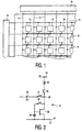
- the active matrix addressed electroluminescent display device comprises a panel having a row and column matrix array of regularly-spaced pixels, denoted by the blocks 10 and comprising electroluminescent display elements together with associated switching means, located at the intersections between crossing sets of row (selection) and column (data) address conductors, or lines, 12 and 14. Only a few pixels are shown in the Figure for simplicity. In practice there may be several hundred rows and columns of pixels.
- the pixels 10 are addressed via the sets of row and column address conductors by a peripheral drive circuit comprising a row, scanning, driver circuit 16 and a column, data, driver circuit 18 connected to the ends of the respective sets of conductors.
- FIG. 2 shows in simplified schematic form the circuit of a typical pixel block 10 in the array and is intended to illustrate the basic manner of its operation.
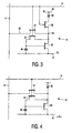
- a practical implementation of the pixel circuit of Figure 2 is illustrated in Figure 3.
- the electroluminescent display element, referenced at 20, comprises an organic light emitting diode, represented here as a diode element (LED) and comprising a pair of electrodes between which one or more active layers of organic electroluminescent material is sandwiched.
- the display elements of the array are carried together with the associated active matrix circuitry on one side of an insulating support. Either the cathodes or the anodes of the display elements are formed of transparent conductive material.
- the support is of transparent material such as glass and the electrodes of the display elements 20 closest to the substrate may consist of a transparent conductive material such as ITO so that light generated by the electroluminescent layer is transmitted through these electrodes and the support so as to be visible to a viewer at the other side of the support.
- the light output is intended to be viewed from above the panel and the display element anodes comprise parts of a continuous ITO layer 22 connected to a potential source and constituting a second supply line common to all display elements in the array and held at a fixed reference potential.
- the cathodes of the display elements comprise a metal having a low work-function such as calcium or a magnesium : silver alloy.
- the thickness of the organic electroluminescent material layer is between 100 nm and 200nm.
- suitable organic electroluminescent materials which can be used for the elements 20 are described in EP-A-0 717446 to which reference is invited for further information and whose disclosure in this respect is incorporated herein.
- Electroluminescent materials such as conjugated polymer materials described in WO96/36959 can also be used.
- Each display element 20 has an associated switch means which is connected to the row and column conductors 12 and 14 adjacent the display element and which is arranged to operate the display element in accordance with an applied analogue drive (data) signal level that determines the element's drive current, and hence light output (grey-scale).
- the display data signals are provided by the column driver circuit 18 which acts as a current source.
- a suitably processed video signal is supplied to this circuit which samples the video signal and applies a current constituting a data signal related to the video information to each of the column conductors in a manner appropriate to row at a time addressing of the array with the operations of the column driver circuit and the scanning row driver circuit being synchronised.
- the switch means comprises a drive transistor 30, more particularly a n - channel FET, whose first current - carrying (source) terminal is connected to a supply line 31 and whose second current - carrying (drain) terminal is connected, via a switch 33, to the cathode of the display element 20.
- the anode of the display element is connected to a second supply line 34, which in effect is constituted by the continuous electrode layer held at a fixed reference potential.
- the gate of the transistor 30 is connected to the supply line 31, and hence the source electrode, via a storage capacitance 38 which may be a separately formed capacitor or the intrinsic gate - source capacitance of the transistor.
- the gate of the transistor 30 is also connected via a switch 32 to its drain terminal.
- the transistor circuit operates in the manner of a single transistor current mirror with the same transistor performing both current sampling and current output functions and with the display element 20 acting as the load.
- An input to this current mirror circuit is provided by an input line 35 which connects to a node 36 between the switches 32 and 33, constituting an input terminal, via a further switch 37 which controls the application of an input signal to the node.
- Operation of the circuit takes place in two phases.
- a first, sampling, phase corresponding in time to an addressing period
- an input signal for determining a required output from the display element is fed into the circuit and a consequential gate - source voltage on the transistor 30 is sampled and stored in the capacitance 38.
- the transistor 30 operates to draw current through the display element 20 according to the level of the stored voltage so as to produce the required output from the display element, as determined by the input signal, which output is maintained for example until the display element is next addressed in a subsequent, new, sampling phase.
- the supply lines 31 and 34 are at appropriate, pre-set, potential levels, V1 and V2.
- the supply line 31 will normally be at ground potential (V1) and the supply line 34 will be at a positive potential (V2).
- the switches 32 and 37 are closed, which diode - connects the transistor 30, and the switch 33 is open, which isolates the display element load.
- An input signal, corresponding to the required display element current and denoted here as lin, is driven through the transistor 30 from an external source, e.g. the column driver circuit 18 in Figure 1, via the input line 35, the closed switch 37 and the input terminal 36. Because the transistor 30 is diode - connected by virtue of the dosed switch 32, the voltage across the capacitance 38 at the steady state condition will be the gate - source voltage that is required to drive a current lin through the channel of the transistor 30.
- the sampling phase is terminated upon the opening of the switches 32 and 37 isolating the input terminal 36 from the input line 35 and isolating the capacitance 38 so that the gate - source voltage, determined in accordance with the input signal lin, is stored in the capacitance 38.
- the output phase then begins upon the closing of the switch 33 thus connecting the display element cathode to the drain of the transistor 30.
- the transistor 30 then operates as a current source and a current approximately equal to lin is drawn through the display element 20.
- the drive current for the display element may differ very slightly from the input current lin because of capacitive coupling due to charge injection effects when switch 32 turns off causing a change in the voltage on capacitance 38 and also because the transistor 30 may not act as a perfect current source as in practice it is likely to have a finite output resistance. Because, however, the same transistor is used to sample lin during the sampling phase and to generate the current during the output phase, the display element current is not dependent on the threshold voltage or the mobility of the transistor 30.
- FIG 3 shows a practical embodiment of the pixel circuit of Figure 2 used in the display device of Figure 1.
- the switches 32, 33 and 37 are each constituted by transistors and these switching transistors, together with the drive transistor 30, are all formed as thin film field effect transistors, TFTs.
- the input line 35, and the corresponding input lines of all pixel circuits in the same column, are connected to a column address conductor 14 and through this to the column driver circuit 18.
- the gates of the transistors 32, 33 and 37, and likewise the gates of the corresponding transistors in pixel circuits in the same row, are all connected to the same row address conductor 12.
- the transistors 32 and 37 comprise n - channel devices and are turned on (closed) by means of a selection (scan) signal in the form of a voltage pulse applied to the row address conductor 12 by the row driver circuit 16.
- the transistor 33 is of opposite conductivity type, comprising a p - channel device, and operates in complementary fashion to the transistors 32 and 37 so that it turns off (opens) when the transistors 32 and 37 are closed in response to a selection signal on the conductor 12. and vice versa.
- the supply line 31 extends as an electrode parallel to the row conductor 12 and is shared by all pixel circuits in the same row.
- the supply lines 31 of all rows can be connected together at their ends.
- the supply lines may instead extend in the column direction with each lines then being shared by the display elements in a respective column.
- supply lines may be provided extending in both the row and column directions and interconnected to form a grid structure.
- the array is driven a row at a time in turn with a selection signal being applied to each row conductor 12 in sequence.
- the duration of the selection signal determines a row address period, corresponding to the period of the aforementioned sampling phase.
- appropriate input current drive signals constituting data signals, are applied to the column conductors 14 by the column driver circuit 18 as required for a row at a time addressing so as to set all the display elements in a selected row to their required drive level simultaneously in a row address period with a respective input signals determining the required display outputs from the display elements. Following addressing of a row in this way, the next row of display elements is addressed in like manner.
- the address sequence is repeated in subsequent field periods with the drive current for a given display element, and hence the output, being set in the respective row address period and maintained for a field period until the row of display elements concerned is next addressed.
- the matrix structure of the array comprising the TFTs, the sets of address lines, the storage capacitors (if provided as discrete components), the display element electrodes and their interconnections, is formed using standard thin film processing technology similar to that used in active matrix LCDs which basically involves the deposition and patterning of various thin film layers of conductive, insulating and semiconductive materials on the surface of an insulating support such as glass or plastics material by CVD deposition and photolithographic patterning techniques. An example of such is described in the aforementioned EP-A-0717446.
- the TFTs may comprise amorphous silicon or polycrystalline silicon TFTs.
- the organic electroluminescent material layer of the display elements may be formed by vapour deposition or by another suitable known technique, such as spin coating.
- the pixel circuit of Figure 3 requires the use of both n and p channel transistors which can complicate the fabrication process. Moreover, this particular circuit requires four transistors and a common electrode whose provision may reduce the effective aperture of the pixel.
- Figure 4 illustrates an alternative, modified, form of pixel circuit which avoids the need to use an opposite polarity type transistor.
- the transistor 33 is removed and the input terminal 36 is connected directly to the display element 20.
- the switching transistors 32 and 37 are closed, through a selection pulse on the associated row conductor 12, which diode - connects the transistor 30.
- the supply line 31 is supplied with a positive voltage pulse, rather than remaining at a constant reference potential as before, so that the display element 20 is reverse - biased.
- the drain current of the transistor 30 is equal to the input current lin.
- the appropriate gate - source voltage of the transistor 30 is again sampled on the capacitance 38.
- the switching transistors 32 and 37 are turned off (opened) as before and the supply line 31 is returned to its normal level, typically OV.
- the transistor 30 operates as before as a current source drawing current through the display element at a level determined by the voltage stored on the capacitor 38.
- a supply line 31 connected separately to a potential source may be provided for each row of pixels.
- the display elements in the row being addressed are turned off (as a result of pulsing the supply line 31) and if there is effectively only one common supply line in the array which is common to all pixel circuits, i.e. the supply line 31 of one row is part of a continuous line interconnecting all rows of pixel circuits, then all the display elements would be turned off during each sampling phase irrespective of which row is being addressed. This would reduce the duty cycle (the ratio of ON to OFF times) for a display element.
- the supply line 31 associated with a row may be kept separate from the supply lines associated with other rows.
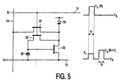
- FIG. 5 Another alternative form of pixel circuit which reduces the overall number of lines in the row direction is shown schematically in Figure 5, together with typical drive waveforms employed in this embodiment.
- the pixel circuit depicted is one in the Nth row of the array and in this arrangement the source of the transistor 30 and the side of the capacitance 38 remote from the gate are both connected to the next, adjacent, row conductor 14 associated with the (N+1)th row of pixels rather than to a separate, dedicated, supply line 31. Operation of this pixel circuit is basically the same as previously described.
- the required row drive waveforms applied to the Nth and (N+1)th row conductors 12 (and all other row conductors) differ from those in the previous embodiments.
- the waveform applied to each row conductor further includes an intermediate level pulse arranged to reverse bias the display element in similar manner to the pulsing of the supply line 31 in the Figure 4 embodiment.
- V s (N) denotes the selection pulse applied to the Nth row conductor to operate the transistors 32 and 37 of the pixel circuits in that row and V s (N+1) denotes the selection signal applied to the next, (N+1)th row conductor which, because the rows are addressed in sequence, occurs after the signal V s (N).
- the waveform for each row conductor includes a positive pulse, Vr, which precedes the selection signal and is coincident in time with the selection signal applied to the preceding row conductor 12 so that when the pixel circuits in the preceding row, i.e.
- V s (N) the positive pulse Vr appearing on the (N+1)th row conductor serves to reverse bias the display elements in the pixel circuits in row N during their sampling phase.
- the level of Vr is selected so as to provide the desired reverse biasing while being lower than the selection signal V s so as to ensure that the transistors 32 of 37 and the pixels circuits in the next, (N+1)th row are not turned on.
- the pixel circuits are based on an n-channel transistor 30, the same modes of operation are possible if the polarity of these transistors is reversed, the display element polarity is reversed, and the polarity of the pulses applied to the supply lines 31 row conductors 12 when used are reversed. Where p-type transistors 33 are used, these would become n-type.
- the material required for the cathode of a display element using organic electroluminescent material would normally have a low work function and typically would comprise a magnesium-based alloy or calcium. Such materials tend to be difficult to pattern photolithographically and hence a continuous layer of such material common to all display elements in the array may be preferred.
- the active matrix circuitry could be fabricated using IC technology on a semiconductor, for example, silicon, substrate.
- the upper electrodes of the LED display elements provided on this substrate would then be formed of transparent conductive material, e.g. ITO, with the light output of the elements being viewed through these upper electrodes.
- switches 32, 33 and 37 need not comprise transistors but may comprise other types of switches, for example, micro-relays or micro-switches.
- the display device may be a monochrome or multi-colour display device. It will be appreciated that a colour display device may be provided by using different light colour emitting display elements in the array. The different colour emitting display elements may typically be provided in a regular, repeating pattern of, for example, red, green and blue colour light emitting display elements.
- an active matrix electroluminescent display device has an array of current - driven electroluminescent display elements, for example comprising organic electroluminescent material, whose operations are each controlled by an associated switching means to which a drive signal for determining a desired light output is supplied in a respective address period and which is arranged to drive the display element according to the drive signal following the address period.
- Each switching means comprises a current mirror circuit in which the same transistor is used to both sense and produce the required drive current for the display element with the gate of the transistor being connected to a storage capacitance on which a voltage determined by the drive signal is stored. This allows variations in transistor characteristics over the array to be compensated and improved uniformity of light outputs from the display elements to be obtained.
Landscapes
- Engineering & Computer Science (AREA)
- Physics & Mathematics (AREA)
- Computer Hardware Design (AREA)
- General Physics & Mathematics (AREA)
- Theoretical Computer Science (AREA)
- Control Of Indicators Other Than Cathode Ray Tubes (AREA)
- Devices For Indicating Variable Information By Combining Individual Elements (AREA)
- Control Of El Displays (AREA)
Abstract
Claims (9)
- Dispositif d'affichage électroluminescent à matrice active comprenant un ensemble matriciel d'éléments d'affichage électroluminescents (10), qui comportent chacun un moyen de commutation associé pour contrôler le courant passant par l'élément d'affichage suivant un signal de commande (35) de courant appliqué et dans lequel le moyen de commutation comprend un transistor de commande (30) dont la première borne sous tension est connectée à une première ligne d'alimentation de potentiel (31), dont la deuxième borne sous tension est connectée par le biais de l'élément d'affichage (20) à une deuxième ligne d'alimentation de potentiel (34) et dont la grille est connectée à sa première borne sous tension par le biais d'une capacité (38),
caractérisé en ce que la deuxième borne sous tension du transistor de commande est connectée à une borne d'entrée pour introduire le signal de commande de courant, et en ce qu'un premier dispositif de commutation (32) est connecté entre la deuxième borne sous tension et la grille du transistor qui est fermé pendant l'application du signal de commande de courant de manière à stocker sur la capacité une tension de grille déterminée par le signal de commande de courant. - Dispositif d'affichage électroluminescent à matrice active suivant la revendication 1, dans lequel les éléments d'affichage sont agencés en rangées et en colonnes, et les dispositifs de commutation du moyen de commutation pour une rangée d'éléments d'affichage sont connectés à un conducteur d'adresse de rangée commun respectif (12) par le biais duquel un signal de sélection destiné à fermer les dispositifs de commutation dans cette rangée, est fourni, et chaque conducteur d'adresse de rangée est prévu pour recevoir le signal de sélection à son tour, de sorte que les rangées des éléments d'affichage sont adressées à raison d'une à la fois de manière successive.
- Dispositif d'affichage électroluminescent à matrice active suivant la revendication 2, dans lequel les signaux de commande pour les éléments d'affichage dans une colonne sont fournis par le biais d'un conducteur d'adresses de colonne respectif (14) commun aux éléments d'affichage de la colonne, un deuxième dispositif de commutation (37) étant connecté entre la borne d'entrée du moyen de commutation d'un élément d'affichage et son conducteur d'adresses de colonne associé, qui est fermé pour transférer un signal de commande sur le conducteur d'adresses de colonne à la borne d'entrée lorsque le premier dispositif de commutation est fermé.
- Dispositif d'affichage électroluminescent à matrice active suivant la revendication 3, dans lequel le deuxième dispositif de commutation est connecté au même conducteur d'adresses de rangée que le premier dispositif de commutation et est fermé en même temps que le premier dispositif de commutation par un signal de sélection appliqué au conducteur d'adresses de rangée.
- Dispositif d'affichage électroluminescent à matrice active suivant l'une quelconque des revendications 2 à 4, dans lequel la première ligne d'alimentation est partagée par tous les éléments d'affichage dans la même rangée ou colonne, la première ligne d'alimentation étant prévue pour chaque rangée ou colonne d'éléments d'affichage.
- Dispositif d'affichage électroluminescent à matrice active suivant la revendication 5, dans lequel la première ligne d'alimentation est associée à et partagée par une rangée d'éléments d'affichage et comprend le conducteur d'adresses de rangée associé à une rangée différente d'éléments d'affichage par le biais duquel le signal de sélection est appliqué aux dispositifs de commutation du moyen de commutation de cette rangée différente.
- Dispositif d'affichage électroluminescent à matrice active suivant l'une quelconque des revendications précédentes, dans lequel un troisième dispositif de commutation (33) est connecté entre la deuxième borne sous tension du transistor de commande et l'élément d'affichage qui est ouvert pour isoler l'élément d'affichage du transistor de commande lorsque le premier dispositif de commutation connecté entre cette borne et la grille du transistor de commande est fermée.
- Dispositif d'affichage électroluminescent à matrice active suivant l'une quelconque des revendications 1 à 6, dans lequel la première ligne d'alimentation est agencée pour recevoir un signal d'impulsion de potentiel pendant l'application d'un signal de commande de courant de manière à polariser dans le sens inverse l'élément d'affichage.
- Dispositif d'affichage électroluminescent à matrice active suivant l'une quelconque des revendications précédentes, dans lequel les transistors de commande et les dispositifs de commutation comprennent des transistors à couches minces supportés sur un substrat isolant.
Applications Claiming Priority (3)
| Application Number | Priority Date | Filing Date | Title |
|---|---|---|---|
| GB9812742 | 1998-06-12 | ||
| GBGB9812742.6A GB9812742D0 (en) | 1998-06-12 | 1998-06-12 | Active matrix electroluminescent display devices |
| PCT/IB1999/001041 WO1999065011A2 (fr) | 1998-06-12 | 1999-06-07 | Dispositifs d'affichage electroluminescents a matrice active |
Publications (2)
| Publication Number | Publication Date |
|---|---|
| EP1034530A2 EP1034530A2 (fr) | 2000-09-13 |
| EP1034530B1 true EP1034530B1 (fr) | 2004-01-21 |
Family
ID=10833684
Family Applications (1)
| Application Number | Title | Priority Date | Filing Date |
|---|---|---|---|
| EP99922419A Expired - Lifetime EP1034530B1 (fr) | 1998-06-12 | 1999-06-07 | Dispositifs d'affichage electroluminescents a matrice active |
Country Status (6)
| Country | Link |
|---|---|
| US (1) | US6373454B1 (fr) |
| EP (1) | EP1034530B1 (fr) |
| JP (1) | JP4965023B2 (fr) |
| DE (1) | DE69914302T2 (fr) |
| GB (1) | GB9812742D0 (fr) |
| WO (1) | WO1999065011A2 (fr) |
Cited By (1)
| Publication number | Priority date | Publication date | Assignee | Title |
|---|---|---|---|---|
| US8629817B2 (en) | 2006-03-10 | 2014-01-14 | Canon Kabushiki Kaisha | Driving circuit of display element and image display apparatus |
Families Citing this family (321)
| Publication number | Priority date | Publication date | Assignee | Title |
|---|---|---|---|---|
| US7071913B2 (en) | 1995-07-20 | 2006-07-04 | E Ink Corporation | Retroreflective electrophoretic displays and materials for making the same |
| US7167155B1 (en) | 1995-07-20 | 2007-01-23 | E Ink Corporation | Color electrophoretic displays |
| US6839158B2 (en) | 1997-08-28 | 2005-01-04 | E Ink Corporation | Encapsulated electrophoretic displays having a monolayer of capsules and materials and methods for making the same |
| US7075502B1 (en) | 1998-04-10 | 2006-07-11 | E Ink Corporation | Full color reflective display with multichromatic sub-pixels |
| US6842657B1 (en) | 1999-04-09 | 2005-01-11 | E Ink Corporation | Reactive formation of dielectric layers and protection of organic layers in organic semiconductor device fabrication |
| US7038655B2 (en) | 1999-05-03 | 2006-05-02 | E Ink Corporation | Electrophoretic ink composed of particles with field dependent mobilities |
| US8115729B2 (en) | 1999-05-03 | 2012-02-14 | E Ink Corporation | Electrophoretic display element with filler particles |
| US7030412B1 (en) | 1999-05-05 | 2006-04-18 | E Ink Corporation | Minimally-patterned semiconductor devices for display applications |
| JP4079198B2 (ja) * | 1999-06-17 | 2008-04-23 | ソニー株式会社 | 画像表示装置及びその駆動方法 |
| WO2001006484A1 (fr) * | 1999-07-14 | 2001-01-25 | Sony Corporation | Circuit d'attaque et affichage le comprenant, circuit de pixels et procede d'attaque |
| US7379039B2 (en) | 1999-07-14 | 2008-05-27 | Sony Corporation | Current drive circuit and display device using same pixel circuit, and drive method |
| EP1196814A1 (fr) * | 1999-07-21 | 2002-04-17 | E Ink Corporation | Utilisation d'un condensateur de memorisation pour ameliorer la performance d'un affichage electronique matriciel actif |
| JP2001109432A (ja) * | 1999-10-06 | 2001-04-20 | Pioneer Electronic Corp | アクティブマトリックス型発光パネルの駆動装置 |
| JP4831862B2 (ja) * | 1999-11-30 | 2011-12-07 | 株式会社半導体エネルギー研究所 | 電子装置 |
| TW587239B (en) | 1999-11-30 | 2004-05-11 | Semiconductor Energy Lab | Electric device |
| JP2001250680A (ja) * | 2000-03-07 | 2001-09-14 | Pioneer Electronic Corp | 発光素子およびその製造方法 |
| JP4954380B2 (ja) * | 2000-03-27 | 2012-06-13 | 株式会社半導体エネルギー研究所 | 発光装置、半導体装置 |
| TW521226B (en) | 2000-03-27 | 2003-02-21 | Semiconductor Energy Lab | Electro-optical device |
| US7893435B2 (en) | 2000-04-18 | 2011-02-22 | E Ink Corporation | Flexible electronic circuits and displays including a backplane comprising a patterned metal foil having a plurality of apertures extending therethrough |
| TW521237B (en) * | 2000-04-18 | 2003-02-21 | Semiconductor Energy Lab | Light emitting device |
| ATE438927T1 (de) * | 2000-04-18 | 2009-08-15 | E Ink Corp | Prozess zur herstellung von dünnfilmtransistoren |
| US7633471B2 (en) * | 2000-05-12 | 2009-12-15 | Semiconductor Energy Laboratory Co., Ltd. | Light-emitting device and electric appliance |
| US6507156B2 (en) * | 2000-05-16 | 2003-01-14 | Planar Systems, Inc. | Display |
| TW493153B (en) * | 2000-05-22 | 2002-07-01 | Koninkl Philips Electronics Nv | Display device |
| JP3822029B2 (ja) * | 2000-06-07 | 2006-09-13 | シャープ株式会社 | 発光器、発光装置、及び表示パネル |
| JP3877049B2 (ja) * | 2000-06-27 | 2007-02-07 | 株式会社日立製作所 | 画像表示装置及びその駆動方法 |
| US6738034B2 (en) | 2000-06-27 | 2004-05-18 | Hitachi, Ltd. | Picture image display device and method of driving the same |
| FR2810983B1 (fr) * | 2000-06-28 | 2004-05-21 | Solvay | Procede de fabrication d'oxiranne au moyen d'un compose peroxyde |
| CN100511369C (zh) | 2000-07-07 | 2009-07-08 | 精工爱普生株式会社 | 用于有机场致发光显示器的电流抽样电路 |
| WO2002005255A1 (fr) * | 2000-07-07 | 2002-01-17 | Seiko Epson Corporation | Dispositif electrooptique d'attaque de courant tel qu'un afficheur electroluminescent organique, avec des transistors d'attaque complementaires destines a contrecarrer les variation de la tension de seuil |
| WO2002071379A2 (fr) * | 2000-07-18 | 2002-09-12 | Emagin Corporation | Circuit de commande de type a courant pour afficheur a diodes lumineuses organiques |
| JP4925528B2 (ja) * | 2000-09-29 | 2012-04-25 | 三洋電機株式会社 | 表示装置 |
| KR100823047B1 (ko) | 2000-10-02 | 2008-04-18 | 가부시키가이샤 한도오따이 에네루기 켄큐쇼 | 자기발광 장치 및 그 구동 방법 |
| JP3937789B2 (ja) * | 2000-10-12 | 2007-06-27 | セイコーエプソン株式会社 | 有機エレクトロルミネッセンス素子を含む駆動回路及び電子機器及び電気光学装置 |
| JP4556957B2 (ja) * | 2000-10-12 | 2010-10-06 | セイコーエプソン株式会社 | 電気光学装置及び電子機器 |
| JP3594126B2 (ja) * | 2000-10-13 | 2004-11-24 | 日本電気株式会社 | 電流駆動回路 |
| SG114502A1 (en) | 2000-10-24 | 2005-09-28 | Semiconductor Energy Lab | Light emitting device and method of driving the same |
| JP3757797B2 (ja) * | 2001-01-09 | 2006-03-22 | 株式会社日立製作所 | 有機ledディスプレイおよびその駆動方法 |
| JP2002215095A (ja) * | 2001-01-22 | 2002-07-31 | Pioneer Electronic Corp | 発光ディスプレイの画素駆動回路 |
| US6912021B2 (en) * | 2001-01-22 | 2005-06-28 | Seiko Epson Corporation | Electro-optical device, method for driving electro-optical device, electronic apparatus, and method for driving electronic apparatus |
| JP4831874B2 (ja) | 2001-02-26 | 2011-12-07 | 株式会社半導体エネルギー研究所 | 発光装置及び電子機器 |
| US6661180B2 (en) | 2001-03-22 | 2003-12-09 | Semiconductor Energy Laboratory Co., Ltd. | Light emitting device, driving method for the same and electronic apparatus |
| US6693385B2 (en) | 2001-03-22 | 2004-02-17 | Semiconductor Energy Laboratory Co., Ltd. | Method of driving a display device |
| US6972742B2 (en) | 2001-05-09 | 2005-12-06 | Clare Micronix Integrated Systems, Inc. | Method of current balancing in visual display devices |
| WO2002091344A2 (fr) * | 2001-05-09 | 2002-11-14 | Clare Micronix Integrated Systems, Inc. | Procede et systeme d'adaptation de courant dans des circuits integres |
| US6943761B2 (en) | 2001-05-09 | 2005-09-13 | Clare Micronix Integrated Systems, Inc. | System for providing pulse amplitude modulation for OLED display drivers |
| US7009590B2 (en) * | 2001-05-15 | 2006-03-07 | Sharp Kabushiki Kaisha | Display apparatus and display method |
| US6975304B1 (en) * | 2001-06-11 | 2005-12-13 | Handspring, Inc. | Interface for processing of an alternate symbol in a computer device |
| US6734636B2 (en) * | 2001-06-22 | 2004-05-11 | International Business Machines Corporation | OLED current drive pixel circuit |
| KR100743103B1 (ko) * | 2001-06-22 | 2007-07-27 | 엘지.필립스 엘시디 주식회사 | 일렉트로 루미네센스 패널 |
| JP2003005710A (ja) | 2001-06-25 | 2003-01-08 | Nec Corp | 電流駆動回路及び画像表示装置 |
| JP4556354B2 (ja) * | 2001-07-09 | 2010-10-06 | セイコーエプソン株式会社 | 駆動回路、装置、及び電子機器 |
| JP2003043994A (ja) * | 2001-07-27 | 2003-02-14 | Canon Inc | アクティブマトリックス型ディスプレイ |
| US6967640B2 (en) * | 2001-07-27 | 2005-11-22 | E Ink Corporation | Microencapsulated electrophoretic display with integrated driver |
| JP2003043995A (ja) * | 2001-07-31 | 2003-02-14 | Matsushita Electric Ind Co Ltd | アクティブマトリックス型oled表示装置およびその駆動方法 |
| JP3951687B2 (ja) * | 2001-08-02 | 2007-08-01 | セイコーエプソン株式会社 | 単位回路の制御に使用されるデータ線の駆動 |
| JP2003114646A (ja) * | 2001-08-03 | 2003-04-18 | Semiconductor Energy Lab Co Ltd | 表示装置及びその駆動方法。 |
| US6876350B2 (en) | 2001-08-10 | 2005-04-05 | Semiconductor Energy Laboratory Co., Ltd. | Display device and electronic equipment using the same |
| US7227517B2 (en) * | 2001-08-23 | 2007-06-05 | Seiko Epson Corporation | Electronic device driving method, electronic device, semiconductor integrated circuit, and electronic apparatus |
| JP5636147B2 (ja) * | 2001-08-28 | 2014-12-03 | パナソニック株式会社 | アクティブマトリックス型表示装置 |
| JP4603233B2 (ja) * | 2001-08-29 | 2010-12-22 | 日本電気株式会社 | 電流負荷素子の駆動回路 |
| CN101257743B (zh) | 2001-08-29 | 2011-05-25 | 株式会社半导体能源研究所 | 发光器件及这种发光器件的驱动方法 |
| US7209101B2 (en) * | 2001-08-29 | 2007-04-24 | Nec Corporation | Current load device and method for driving the same |
| DE60239582D1 (de) * | 2001-08-29 | 2011-05-12 | Nec Corp | Treiber für eine TFT-Displaymatrix |
| JP4650601B2 (ja) * | 2001-09-05 | 2011-03-16 | 日本電気株式会社 | 電流駆動素子の駆動回路及び駆動方法ならびに画像表示装置 |
| US11302253B2 (en) | 2001-09-07 | 2022-04-12 | Joled Inc. | El display apparatus |
| CN1552050B (zh) | 2001-09-07 | 2010-10-06 | 松下电器产业株式会社 | El显示装置及其驱动方法 |
| WO2003023752A1 (fr) | 2001-09-07 | 2003-03-20 | Matsushita Electric Industrial Co., Ltd. | Affichage el, circuit d'entrainement d'affichage el et affichage d'image |
| JP2010122700A (ja) * | 2001-09-10 | 2010-06-03 | Seiko Epson Corp | 電気光学装置及び電子機器 |
| JP4581893B2 (ja) * | 2001-09-10 | 2010-11-17 | セイコーエプソン株式会社 | 電子装置、及び電子機器 |
| JP4075505B2 (ja) | 2001-09-10 | 2008-04-16 | セイコーエプソン株式会社 | 電子回路、電子装置、及び電子機器 |
| TW563088B (en) * | 2001-09-17 | 2003-11-21 | Semiconductor Energy Lab | Light emitting device, method of driving a light emitting device, and electronic equipment |
| US20040239654A1 (en) * | 2001-09-20 | 2004-12-02 | Yoshiyuki Okuda | Drive circuit for light emitting elements |
| CN107230450A (zh) | 2001-09-21 | 2017-10-03 | 株式会社半导体能源研究所 | 显示装置及其驱动方法 |
| SG120075A1 (en) | 2001-09-21 | 2006-03-28 | Semiconductor Energy Lab | Semiconductor device |
| JP3810725B2 (ja) * | 2001-09-21 | 2006-08-16 | 株式会社半導体エネルギー研究所 | 発光装置及び電子機器 |
| JP2006338042A (ja) * | 2001-09-21 | 2006-12-14 | Semiconductor Energy Lab Co Ltd | 発光装置、発光装置の駆動方法 |
| US20050057580A1 (en) * | 2001-09-25 | 2005-03-17 | Atsuhiro Yamano | El display panel and el display apparatus comprising it |
| JP5470668B2 (ja) * | 2001-09-28 | 2014-04-16 | パナソニック株式会社 | アクティブマトリクス型表示装置 |
| US6777885B2 (en) * | 2001-10-12 | 2004-08-17 | Semiconductor Energy Laboratory Co., Ltd. | Drive circuit, display device using the drive circuit and electronic apparatus using the display device |
| US7365713B2 (en) | 2001-10-24 | 2008-04-29 | Semiconductor Energy Laboratory Co., Ltd. | Semiconductor device and driving method thereof |
| US7456810B2 (en) | 2001-10-26 | 2008-11-25 | Semiconductor Energy Laboratory Co., Ltd. | Light-emitting device and driving method thereof |
| JP4498669B2 (ja) | 2001-10-30 | 2010-07-07 | 株式会社半導体エネルギー研究所 | 半導体装置、表示装置、及びそれらを具備する電子機器 |
| US7576734B2 (en) * | 2001-10-30 | 2009-08-18 | Semiconductor Energy Laboratory Co., Ltd. | Signal line driving circuit, light emitting device, and method for driving the same |
| US7742064B2 (en) | 2001-10-30 | 2010-06-22 | Semiconductor Energy Laboratory Co., Ltd | Signal line driver circuit, light emitting device and driving method thereof |
| US7180479B2 (en) | 2001-10-30 | 2007-02-20 | Semiconductor Energy Laboratory Co., Ltd. | Signal line drive circuit and light emitting device and driving method therefor |
| US7193619B2 (en) | 2001-10-31 | 2007-03-20 | Semiconductor Energy Laboratory Co., Ltd. | Signal line driving circuit and light emitting device |
| TWI261217B (en) | 2001-10-31 | 2006-09-01 | Semiconductor Energy Lab | Driving circuit of signal line and light emitting apparatus |
| JP4202012B2 (ja) | 2001-11-09 | 2008-12-24 | 株式会社半導体エネルギー研究所 | 発光装置及び電流記憶回路 |
| US7202847B2 (en) | 2002-06-28 | 2007-04-10 | E Ink Corporation | Voltage modulated driver circuits for electro-optic displays |
| US7483001B2 (en) * | 2001-11-21 | 2009-01-27 | Seiko Epson Corporation | Active matrix substrate, electro-optical device, and electronic device |
| TW529006B (en) * | 2001-11-28 | 2003-04-21 | Ind Tech Res Inst | Array circuit of light emitting diode display |
| US6865010B2 (en) | 2001-12-13 | 2005-03-08 | E Ink Corporation | Electrophoretic electronic displays with low-index films |
| JP2003195810A (ja) | 2001-12-28 | 2003-07-09 | Casio Comput Co Ltd | 駆動回路、駆動装置及び光学要素の駆動方法 |
| GB2384100B (en) * | 2002-01-09 | 2005-10-26 | Seiko Epson Corp | An electronic circuit for controlling the current supply to an element |
| JP2003216100A (ja) * | 2002-01-21 | 2003-07-30 | Matsushita Electric Ind Co Ltd | El表示パネルとel表示装置およびその駆動方法および表示装置の検査方法とel表示装置のドライバ回路 |
| US6900851B2 (en) | 2002-02-08 | 2005-05-31 | E Ink Corporation | Electro-optic displays and optical systems for addressing such displays |
| GB0205859D0 (en) * | 2002-03-13 | 2002-04-24 | Koninkl Philips Electronics Nv | Electroluminescent display device |
| JP2004004788A (ja) | 2002-04-24 | 2004-01-08 | Seiko Epson Corp | 電子素子の制御回路、電子回路、電気光学装置、電気光学装置の駆動方法、及び電子機器、並びに電子素子の制御方法 |
| JP3637911B2 (ja) | 2002-04-24 | 2005-04-13 | セイコーエプソン株式会社 | 電子装置、電子機器、および電子装置の駆動方法 |
| KR100702103B1 (ko) | 2002-04-26 | 2007-04-02 | 도시바 마쯔시따 디스플레이 테크놀로지 컴퍼니, 리미티드 | El 표시 장치의 구동 방법 |
| CN1983365B (zh) * | 2002-04-26 | 2011-05-18 | 东芝松下显示技术有限公司 | 用于场致发光显示屏的驱动电路 |
| JP2008003620A (ja) * | 2002-04-26 | 2008-01-10 | Toshiba Matsushita Display Technology Co Ltd | El表示装置 |
| WO2003091977A1 (fr) | 2002-04-26 | 2003-11-06 | Toshiba Matsushita Display Technology Co., Ltd. | Circuit de commande d'un ecran el |
| CN100536347C (zh) | 2002-04-26 | 2009-09-02 | 东芝松下显示技术有限公司 | 电流驱动型显示装置的驱动用半导体电路组及显示装置 |
| SG119186A1 (en) | 2002-05-17 | 2006-02-28 | Semiconductor Energy Lab | Display apparatus and driving method thereof |
| US7170479B2 (en) | 2002-05-17 | 2007-01-30 | Semiconductor Energy Laboratory Co., Ltd. | Display device and driving method thereof |
| TWI360098B (en) | 2002-05-17 | 2012-03-11 | Semiconductor Energy Lab | Display apparatus and driving method thereof |
| US7474285B2 (en) | 2002-05-17 | 2009-01-06 | Semiconductor Energy Laboratory Co., Ltd. | Display apparatus and driving method thereof |
| US7184034B2 (en) | 2002-05-17 | 2007-02-27 | Semiconductor Energy Laboratory Co., Ltd. | Display device |
| JP3918642B2 (ja) | 2002-06-07 | 2007-05-23 | カシオ計算機株式会社 | 表示装置及びその駆動方法 |
| JP3972359B2 (ja) * | 2002-06-07 | 2007-09-05 | カシオ計算機株式会社 | 表示装置 |
| JP4610843B2 (ja) * | 2002-06-20 | 2011-01-12 | カシオ計算機株式会社 | 表示装置及び表示装置の駆動方法 |
| TW594628B (en) * | 2002-07-12 | 2004-06-21 | Au Optronics Corp | Cell pixel driving circuit of OLED |
| GB0218170D0 (en) * | 2002-08-06 | 2002-09-11 | Koninkl Philips Electronics Nv | Electroluminescent display devices |
| US7312916B2 (en) | 2002-08-07 | 2007-12-25 | E Ink Corporation | Electrophoretic media containing specularly reflective particles |
| EP1532610A2 (fr) * | 2002-08-21 | 2005-05-25 | Koninklijke Philips Electronics N.V. | Dispositif d'affichage |
| JP4103500B2 (ja) | 2002-08-26 | 2008-06-18 | カシオ計算機株式会社 | 表示装置及び表示パネルの駆動方法 |
| JP2004145278A (ja) | 2002-08-30 | 2004-05-20 | Seiko Epson Corp | 電子回路、電子回路の駆動方法、電気光学装置、電気光学装置の駆動方法及び電子機器 |
| JP4194451B2 (ja) * | 2002-09-02 | 2008-12-10 | キヤノン株式会社 | 駆動回路及び表示装置及び情報表示装置 |
| JP4416456B2 (ja) * | 2002-09-02 | 2010-02-17 | キヤノン株式会社 | エレクトロルミネッセンス装置 |
| JP3984938B2 (ja) * | 2002-09-02 | 2007-10-03 | キヤノン株式会社 | シフトレジスタ及び表示装置及び情報表示装置 |
| JP4350463B2 (ja) * | 2002-09-02 | 2009-10-21 | キヤノン株式会社 | 入力回路及び表示装置及び情報表示装置 |
| GB0220614D0 (en) * | 2002-09-05 | 2002-10-16 | Koninkl Philips Electronics Nv | Electroluminescent display devices |
| JP2006072385A (ja) * | 2002-10-03 | 2006-03-16 | Seiko Epson Corp | 電子装置及び電子機器 |
| JP2004145300A (ja) | 2002-10-03 | 2004-05-20 | Seiko Epson Corp | 電子回路、電子回路の駆動方法、電子装置、電気光学装置、電気光学装置の駆動方法及び電子機器 |
| JP4201765B2 (ja) | 2002-10-09 | 2008-12-24 | 三菱電機株式会社 | 画像表示素子のデータ線駆動回路および画像表示装置 |
| JP2004138773A (ja) * | 2002-10-17 | 2004-05-13 | Tohoku Pioneer Corp | アクティブ型発光表示装置 |
| CN100375144C (zh) | 2002-11-06 | 2008-03-12 | 三菱电机株式会社 | 采样保持电路以及使用它的图像显示装置 |
| EP1576380A1 (fr) * | 2002-11-06 | 2005-09-21 | Koninklijke Philips Electronics N.V. | Procede et dispositif d'inspection pour affichage a matrice de del |
| US20050212448A1 (en) * | 2002-11-20 | 2005-09-29 | Makoto Shibusawa | Organic EL display and active matrix substrate |
| CN1711577A (zh) * | 2002-11-20 | 2005-12-21 | 东芝松下显示技术有限公司 | 有机el显示器和有源矩阵基板 |
| TWI470607B (zh) * | 2002-11-29 | 2015-01-21 | Semiconductor Energy Lab | A current driving circuit and a display device using the same |
| JP4566528B2 (ja) | 2002-12-05 | 2010-10-20 | シャープ株式会社 | 表示装置 |
| US7573442B2 (en) | 2002-12-06 | 2009-08-11 | Toshiba Matsushita Display Technology Co., Ltd. | Display, active matrix substrate, and driving method |
| CN1723622B (zh) | 2002-12-10 | 2011-08-24 | 株式会社半导体能源研究所 | 半导体装置、数字模拟转换电路和采用它们的具有灰度校正功能的显示器 |
| WO2004061812A1 (fr) | 2002-12-27 | 2004-07-22 | Semiconductor Energy Laboratory Co., Ltd. | Dispositif a semi-conducteur et ecran mettant ce dernier en application |
| EP1585098A4 (fr) | 2003-01-17 | 2007-03-21 | Semiconductor Energy Lab | Circuit d'alimentation, circuit d'entrainement de ligne de signal, son procede d'entrainement, et dispositif electroluminescent |
| KR100732106B1 (ko) | 2003-01-22 | 2007-06-27 | 도시바 마쯔시따 디스플레이 테크놀로지 컴퍼니, 리미티드 | 유기 el 디스플레이 및 액티브 매트릭스 기판 |
| JP4550372B2 (ja) * | 2003-05-16 | 2010-09-22 | 東芝モバイルディスプレイ株式会社 | アクティブマトリクス型表示装置 |
| JP4048969B2 (ja) * | 2003-02-12 | 2008-02-20 | セイコーエプソン株式会社 | 電気光学装置の駆動方法及び電子機器 |
| JP4378087B2 (ja) * | 2003-02-19 | 2009-12-02 | 奇美電子股▲ふん▼有限公司 | 画像表示装置 |
| JP3952965B2 (ja) | 2003-02-25 | 2007-08-01 | カシオ計算機株式会社 | 表示装置及び表示装置の駆動方法 |
| CN102360538B (zh) | 2003-02-28 | 2015-09-02 | 株式会社半导体能源研究所 | 半导体装置及其驱动方法 |
| JP4703103B2 (ja) * | 2003-03-05 | 2011-06-15 | 東芝モバイルディスプレイ株式会社 | アクティブマトリックス型のel表示装置の駆動方法 |
| TWI228696B (en) * | 2003-03-21 | 2005-03-01 | Ind Tech Res Inst | Pixel circuit for active matrix OLED and driving method |
| JP4166783B2 (ja) * | 2003-03-26 | 2008-10-15 | 株式会社半導体エネルギー研究所 | 発光装置及び素子基板 |
| JP4619289B2 (ja) | 2003-03-26 | 2011-01-26 | 株式会社半導体エネルギー研究所 | 表示装置及びその駆動方法、並びに電子機器 |
| JP4197287B2 (ja) | 2003-03-28 | 2008-12-17 | シャープ株式会社 | 表示装置 |
| JP4558509B2 (ja) | 2003-04-25 | 2010-10-06 | 株式会社半導体エネルギー研究所 | 半導体装置、表示装置、及び電子機器 |
| US7561147B2 (en) | 2003-05-07 | 2009-07-14 | Toshiba Matsushita Display Technology Co., Ltd. | Current output type of semiconductor circuit, source driver for display drive, display device, and current output method |
| EP1624435A1 (fr) * | 2003-05-07 | 2006-02-08 | Toshiba Matsushita Display Technology Co., Ltd. | Afficheur el et son procede d'excitation |
| US7453427B2 (en) | 2003-05-09 | 2008-11-18 | Semiconductor Energy Laboratory Co., Ltd. | Semiconductor device and driving method thereof |
| EP1624436A4 (fr) * | 2003-05-13 | 2009-04-15 | Toshiba Matsushita Display Tec | Dispositif d'affichage de type a matrice active |
| EP1624358B1 (fr) | 2003-05-14 | 2015-03-11 | Semiconductor Energy Laboratory Co., Ltd. | Dispositif semi-conducteur |
| US7566902B2 (en) | 2003-05-16 | 2009-07-28 | Semiconductor Energy Laboratory Co., Ltd. | Light-emitting device and electronic device |
| JP4467910B2 (ja) * | 2003-05-16 | 2010-05-26 | 東芝モバイルディスプレイ株式会社 | アクティブマトリクス型表示装置 |
| JP2004341353A (ja) * | 2003-05-16 | 2004-12-02 | Toshiba Matsushita Display Technology Co Ltd | アクティブマトリクス型表示装置 |
| JP4016962B2 (ja) | 2003-05-19 | 2007-12-05 | セイコーエプソン株式会社 | 電気光学装置、電気光学装置の駆動方法 |
| JP2004361753A (ja) * | 2003-06-05 | 2004-12-24 | Chi Mei Electronics Corp | 画像表示装置 |
| JP2004361737A (ja) * | 2003-06-05 | 2004-12-24 | Nippon Hoso Kyokai <Nhk> | 有機発光ダイオード駆動回路及びそれを用いたディスプレイ装置 |
| CN102201196B (zh) | 2003-06-06 | 2014-03-26 | 株式会社半导体能源研究所 | 半导体装置 |
| US6998788B2 (en) * | 2003-06-11 | 2006-02-14 | Au Optronics Corporation | Architecture of data driver applied at display elements with current-driven pixels |
| TW200500926A (en) * | 2003-06-17 | 2005-01-01 | Darfon Electronics Corp | Light emitting module and keyboard using the same |
| JP4662698B2 (ja) * | 2003-06-25 | 2011-03-30 | ルネサスエレクトロニクス株式会社 | 電流源回路、並びに電流設定方法 |
| GB0315929D0 (en) * | 2003-07-08 | 2003-08-13 | Koninkl Philips Electronics Nv | Display device |
| US8378939B2 (en) | 2003-07-11 | 2013-02-19 | Semiconductor Energy Laboratory Co., Ltd. | Semiconductor device |
| US7961160B2 (en) * | 2003-07-31 | 2011-06-14 | Semiconductor Energy Laboratory Co., Ltd. | Display device, a driving method of a display device, and a semiconductor integrated circuit incorporated in a display device |
| US8085226B2 (en) | 2003-08-15 | 2011-12-27 | Semiconductor Energy Laboratory Co., Ltd. | Semiconductor device |
| US8350785B2 (en) | 2003-09-12 | 2013-01-08 | Semiconductor Energy Laboratory Co., Ltd. | Semiconductor device and driving method of the same |
| CA2443206A1 (fr) | 2003-09-23 | 2005-03-23 | Ignis Innovation Inc. | Panneaux arriere d'ecran amoled - circuits de commande des pixels, architecture de reseau et compensation externe |
| US7193588B2 (en) * | 2003-09-29 | 2007-03-20 | Wintek Corporation | Active matrix organic electroluminescence display driving circuit |
| KR100599726B1 (ko) * | 2003-11-27 | 2006-07-12 | 삼성에스디아이 주식회사 | 발광 표시 장치 및 그 표시 패널과 구동 방법 |
| JP4297438B2 (ja) * | 2003-11-24 | 2009-07-15 | 三星モバイルディスプレイ株式會社 | 発光表示装置,表示パネル,及び発光表示装置の駆動方法 |
| JP4054794B2 (ja) | 2003-12-04 | 2008-03-05 | キヤノン株式会社 | 駆動装置及び表示装置及び記録装置 |
| JP4203656B2 (ja) * | 2004-01-16 | 2009-01-07 | カシオ計算機株式会社 | 表示装置及び表示パネルの駆動方法 |
| JP4263153B2 (ja) | 2004-01-30 | 2009-05-13 | Necエレクトロニクス株式会社 | 表示装置、表示装置の駆動回路およびその駆動回路用半導体デバイス |
| US7339560B2 (en) * | 2004-02-12 | 2008-03-04 | Au Optronics Corporation | OLED pixel |
| US7173585B2 (en) | 2004-03-10 | 2007-02-06 | Wintek Corporation | Active matrix display driving circuit |
| JP2005275315A (ja) * | 2004-03-26 | 2005-10-06 | Semiconductor Energy Lab Co Ltd | 表示装置、その駆動方法及びそれを用いた電子機器 |
| JP4665419B2 (ja) | 2004-03-30 | 2011-04-06 | カシオ計算機株式会社 | 画素回路基板の検査方法及び検査装置 |
| US20050224197A1 (en) * | 2004-04-12 | 2005-10-13 | Cheng Wen P | Combining device for tightly fixing screen to wall |
| US6977470B2 (en) * | 2004-04-28 | 2005-12-20 | Au Optronics Corp. | Current-driven OLED pixel |
| TWI288900B (en) * | 2004-04-30 | 2007-10-21 | Fujifilm Corp | Active matrix type display device |
| US8355015B2 (en) | 2004-05-21 | 2013-01-15 | Semiconductor Energy Laboratory Co., Ltd. | Semiconductor device, display device and electronic device including a diode electrically connected to a signal line |
| US20050258867A1 (en) * | 2004-05-21 | 2005-11-24 | Seiko Epson Corporation | Electronic circuit, electro-optical device, electronic device and electronic apparatus |
| JP2005352063A (ja) | 2004-06-09 | 2005-12-22 | Mitsubishi Electric Corp | 画像表示装置 |
| US20050275352A1 (en) * | 2004-06-14 | 2005-12-15 | Au Optronics Corporation. | Redundant storage capacitor and method for repairing OLED pixels and driving circuits |
| US7608861B2 (en) * | 2004-06-24 | 2009-10-27 | Canon Kabushiki Kaisha | Active matrix type display having two transistors of opposite conductivity acting as a single switch for the driving transistor of a display element |
| EP1610292B1 (fr) | 2004-06-25 | 2016-06-15 | Semiconductor Energy Laboratory Co., Ltd. | Dispositif de visualisation et son procédé de commande |
| CA2472671A1 (fr) | 2004-06-29 | 2005-12-29 | Ignis Innovation Inc. | Procede de programmation par tensions pour affichages a del excitees par courant |
| WO2006030544A1 (fr) * | 2004-09-14 | 2006-03-23 | Toshiba Matsushita Display Technology Co., Ltd. | Affichage, substrat de reseau et procede de fabrication de l'affichage |
| JP4192133B2 (ja) * | 2004-09-28 | 2008-12-03 | 東芝松下ディスプレイテクノロジー株式会社 | 表示装置及びその駆動方法 |
| JP4501785B2 (ja) | 2004-09-30 | 2010-07-14 | セイコーエプソン株式会社 | 画素回路及び電子機器 |
| KR100602352B1 (ko) * | 2004-11-22 | 2006-07-18 | 삼성에스디아이 주식회사 | 화소 및 이를 이용한 발광 표시장치 |
| JP4438066B2 (ja) * | 2004-11-26 | 2010-03-24 | キヤノン株式会社 | アクティブマトリクス型表示装置およびその電流プログラミング方法 |
| US7502040B2 (en) * | 2004-12-06 | 2009-03-10 | Semiconductor Energy Laboratory Co., Ltd. | Display device, driving method thereof and electronic appliance |
| US8576217B2 (en) | 2011-05-20 | 2013-11-05 | Ignis Innovation Inc. | System and methods for extraction of threshold and mobility parameters in AMOLED displays |
| US9275579B2 (en) | 2004-12-15 | 2016-03-01 | Ignis Innovation Inc. | System and methods for extraction of threshold and mobility parameters in AMOLED displays |
| WO2006063448A1 (fr) | 2004-12-15 | 2006-06-22 | Ignis Innovation Inc. | Procede et systeme de programmation, de calibrage et de commande d'un affichage a dispositif electroluminescent |
| US10012678B2 (en) | 2004-12-15 | 2018-07-03 | Ignis Innovation Inc. | Method and system for programming, calibrating and/or compensating, and driving an LED display |
| US8599191B2 (en) | 2011-05-20 | 2013-12-03 | Ignis Innovation Inc. | System and methods for extraction of threshold and mobility parameters in AMOLED displays |
| US10013907B2 (en) | 2004-12-15 | 2018-07-03 | Ignis Innovation Inc. | Method and system for programming, calibrating and/or compensating, and driving an LED display |
| US9171500B2 (en) | 2011-05-20 | 2015-10-27 | Ignis Innovation Inc. | System and methods for extraction of parasitic parameters in AMOLED displays |
| US9280933B2 (en) | 2004-12-15 | 2016-03-08 | Ignis Innovation Inc. | System and methods for extraction of threshold and mobility parameters in AMOLED displays |
| US20140111567A1 (en) | 2005-04-12 | 2014-04-24 | Ignis Innovation Inc. | System and method for compensation of non-uniformities in light emitting device displays |
| US9799246B2 (en) | 2011-05-20 | 2017-10-24 | Ignis Innovation Inc. | System and methods for extraction of threshold and mobility parameters in AMOLED displays |
| JP2006184577A (ja) * | 2004-12-27 | 2006-07-13 | Toshiba Matsushita Display Technology Co Ltd | 表示装置、アレイ基板、及び表示装置の製造方法 |
| JP2006184576A (ja) * | 2004-12-27 | 2006-07-13 | Toshiba Matsushita Display Technology Co Ltd | 自発光型表示装置及びアレイ基板 |
| US20060139265A1 (en) * | 2004-12-28 | 2006-06-29 | Semiconductor Energy Laboratory Co., Ltd. | Driving method of display device |
| US20060158399A1 (en) | 2005-01-14 | 2006-07-20 | Semiconductor Energy Laboratory Co., Ltd. | Driving method of display device |
| US7746299B2 (en) * | 2005-01-31 | 2010-06-29 | Toshiba Matsushita Display Technology Co., Ltd. | Display, array substrate, and method of driving display |
| JP4987310B2 (ja) * | 2005-01-31 | 2012-07-25 | 株式会社ジャパンディスプレイセントラル | 表示装置、アレイ基板、及び表示装置の駆動方法 |
| CA2496642A1 (fr) | 2005-02-10 | 2006-08-10 | Ignis Innovation Inc. | Methode d'attaque a courte duree de stabilisation pour afficheurs a diodes organiques electroluminescentes (oled) programmes par courant |
| WO2006092900A1 (fr) * | 2005-02-28 | 2006-09-08 | Toshiba Matsushita Display Technology Co., Ltd. | Affichage et procede de fabrication de celui-ci |
| JP2006251049A (ja) * | 2005-03-08 | 2006-09-21 | Toshiba Matsushita Display Technology Co Ltd | 表示装置及びアレイ基板 |
| US7355220B2 (en) * | 2005-03-31 | 2008-04-08 | Toshiba Matsushita Display Technology Co., Ltd. | Array substrate |
| US20060221005A1 (en) * | 2005-03-31 | 2006-10-05 | Kazuyoshi Omata | Display, array substrate, and method of driving display |
| JP2006284945A (ja) * | 2005-03-31 | 2006-10-19 | Toshiba Matsushita Display Technology Co Ltd | 表示装置及びその駆動方法 |
| JP2006284914A (ja) * | 2005-03-31 | 2006-10-19 | Toshiba Matsushita Display Technology Co Ltd | 表示装置及びその駆動方法 |
| JP2006284916A (ja) * | 2005-03-31 | 2006-10-19 | Toshiba Matsushita Display Technology Co Ltd | 表示装置、アレイ基板、及び表示装置の駆動方法 |
| JP2006309110A (ja) * | 2005-03-31 | 2006-11-09 | Toshiba Matsushita Display Technology Co Ltd | 表示装置、アレイ基板、及び表示装置の製造方法 |
| JP2006284944A (ja) * | 2005-03-31 | 2006-10-19 | Toshiba Matsushita Display Technology Co Ltd | 表示装置、アレイ基板、及び表示装置の駆動方法 |
| US7719526B2 (en) | 2005-04-14 | 2010-05-18 | Semiconductor Energy Laboratory Co., Ltd. | Display device, and driving method and electronic apparatus of the display device |
| US8633919B2 (en) * | 2005-04-14 | 2014-01-21 | Semiconductor Energy Laboratory Co., Ltd. | Display device, driving method of the display device, and electronic device |
| EP1720148A3 (fr) | 2005-05-02 | 2007-09-05 | Semiconductor Energy Laboratory Co., Ltd. | Dispositif d'affichage et son procédé de commande d'échelle des gris avec sous-trames |
| KR20080032072A (ko) | 2005-06-08 | 2008-04-14 | 이그니스 이노베이션 인크. | 발광 디바이스 디스플레이 구동 방법 및 시스템 |
| JP2007003792A (ja) * | 2005-06-23 | 2007-01-11 | Toshiba Matsushita Display Technology Co Ltd | 表示装置及びアレイ基板 |
| JP4826158B2 (ja) * | 2005-07-25 | 2011-11-30 | セイコーエプソン株式会社 | 電気光学装置 |
| US20070018917A1 (en) * | 2005-07-15 | 2007-01-25 | Seiko Epson Corporation | Electronic device, method of driving the same, electro-optical device, and electronic apparatus |
| TWI485681B (zh) * | 2005-08-12 | 2015-05-21 | 半導體能源研究所股份有限公司 | 顯示裝置 |
| CA2518276A1 (fr) | 2005-09-13 | 2007-03-13 | Ignis Innovation Inc. | Technique de compensation de la degradation de luminance dans des dispositifs electroluminescents |
| EP1764770A3 (fr) | 2005-09-16 | 2012-03-14 | Semiconductor Energy Laboratory Co., Ltd. | Dispositif d'affichage et procédé de commande du dispositif d'affichage |
| JP4556814B2 (ja) * | 2005-09-16 | 2010-10-06 | セイコーエプソン株式会社 | 装置、装置の駆動方法及び電子機器 |
| JP2006072377A (ja) * | 2005-09-16 | 2006-03-16 | Seiko Epson Corp | 回路、装置、及び電子機器 |
| JP2007133351A (ja) * | 2005-10-12 | 2007-05-31 | Canon Inc | 表示装置、アクティブマトリクス装置およびそれらの駆動方法 |
| EP1777690B1 (fr) | 2005-10-18 | 2012-08-01 | Semiconductor Energy Laboratory Co., Ltd. | Dispositif d'affichage |
| JP4991138B2 (ja) * | 2005-10-20 | 2012-08-01 | 株式会社ジャパンディスプレイセントラル | アクティブマトリックス型表示装置の駆動方法及び駆動装置 |
| JP2007121629A (ja) * | 2005-10-27 | 2007-05-17 | Canon Inc | アクティブマトリクス型表示装置およびカメラ |
| KR100916866B1 (ko) * | 2005-12-01 | 2009-09-09 | 도시바 모바일 디스플레이 가부시키가이샤 | El 표시 장치와 el 표시 장치의 구동 방법 |
| EP1793367A3 (fr) | 2005-12-02 | 2009-08-26 | Semiconductor Energy Laboratory Co., Ltd. | Dispositif semiconducteur |
| KR101404582B1 (ko) * | 2006-01-20 | 2014-06-09 | 가부시키가이샤 한도오따이 에네루기 켄큐쇼 | 표시장치의 구동방법 |
| KR100965022B1 (ko) * | 2006-02-20 | 2010-06-21 | 도시바 모바일 디스플레이 가부시키가이샤 | El 표시 장치 및 el 표시 장치의 구동 방법 |
| JP5224702B2 (ja) | 2006-03-13 | 2013-07-03 | キヤノン株式会社 | 画素回路、及び当該画素回路を有する画像表示装置 |
| TWI279763B (en) * | 2006-03-13 | 2007-04-21 | Himax Tech Ltd | Light emitting display, pixel circuit and driving method thereof |
| US7616179B2 (en) * | 2006-03-31 | 2009-11-10 | Canon Kabushiki Kaisha | Organic EL display apparatus and driving method therefor |
| KR100784014B1 (ko) * | 2006-04-17 | 2007-12-07 | 삼성에스디아이 주식회사 | 유기전계발광 표시장치 및 그의 구동방법 |
| US8477121B2 (en) | 2006-04-19 | 2013-07-02 | Ignis Innovation, Inc. | Stable driving scheme for active matrix displays |
| JP4208903B2 (ja) * | 2006-06-30 | 2009-01-14 | キヤノン株式会社 | アクティブマトリクス型表示装置及びそれを用いた情報処理装置 |
| JP5196744B2 (ja) * | 2006-06-30 | 2013-05-15 | キヤノン株式会社 | アクティブマトリクス型の表示装置 |
| JP4208902B2 (ja) * | 2006-06-30 | 2009-01-14 | キヤノン株式会社 | アクティブマトリクス型表示装置およびその駆動方法 |
| CA2556961A1 (fr) | 2006-08-15 | 2008-02-15 | Ignis Innovation Inc. | Technique de compensation de diodes electroluminescentes organiques basee sur leur capacite |
| WO2008029717A1 (fr) * | 2006-09-05 | 2008-03-13 | Canon Kabushiki Kaisha | Dispositif d'affichage émettant de la lumière organique |
| JP5665256B2 (ja) * | 2006-12-20 | 2015-02-04 | キヤノン株式会社 | 発光表示デバイス |
| US7355574B1 (en) * | 2007-01-24 | 2008-04-08 | Eastman Kodak Company | OLED display with aging and efficiency compensation |
| JP5361139B2 (ja) * | 2007-03-09 | 2013-12-04 | キヤノン株式会社 | 表示装置 |
| JP2009104104A (ja) * | 2007-05-30 | 2009-05-14 | Canon Inc | アクティブマトリックスディスプレイおよびその駆動方法 |
| JP2008298970A (ja) * | 2007-05-30 | 2008-12-11 | Canon Inc | 有機el画素回路及びその駆動方法 |
| JP4969322B2 (ja) * | 2007-06-01 | 2012-07-04 | 三菱電機株式会社 | 電圧発生回路およびそれを備える画像表示装置 |
| JP5495510B2 (ja) * | 2007-06-19 | 2014-05-21 | キヤノン株式会社 | 表示装置及びそれを用いた電子機器 |
| US20090006198A1 (en) * | 2007-06-29 | 2009-01-01 | David George Walsh | Product displays for retail stores |
| JP2009014836A (ja) * | 2007-07-02 | 2009-01-22 | Canon Inc | アクティブマトリクス型表示装置及びその駆動方法 |
| JP2009037123A (ja) * | 2007-08-03 | 2009-02-19 | Canon Inc | アクティブマトリクス型表示装置及びその駆動方法 |
| WO2009025387A1 (fr) * | 2007-08-21 | 2009-02-26 | Canon Kabushiki Kaisha | Appareil d'affichage et son procédé de commande |
| US20090066615A1 (en) * | 2007-09-11 | 2009-03-12 | Canon Kabushiki Kaisha | Display apparatus and driving method thereof |
| JP2009080272A (ja) * | 2007-09-26 | 2009-04-16 | Canon Inc | アクティブマトリクス型表示装置 |
| JP2009109641A (ja) * | 2007-10-29 | 2009-05-21 | Canon Inc | 駆動回路、及びアクティブマトリクス型表示装置 |
| JP2008146051A (ja) * | 2007-11-22 | 2008-06-26 | Toshiba Matsushita Display Technology Co Ltd | El表示装置 |
| US8339040B2 (en) * | 2007-12-18 | 2012-12-25 | Lumimove, Inc. | Flexible electroluminescent devices and systems |
| JP2009265410A (ja) * | 2008-04-25 | 2009-11-12 | Toshiba Mobile Display Co Ltd | アクティブマトリクス型表示装置 |
| JP2010008987A (ja) * | 2008-06-30 | 2010-01-14 | Canon Inc | 駆動回路 |
| US9311859B2 (en) | 2009-11-30 | 2016-04-12 | Ignis Innovation Inc. | Resetting cycle for aging compensation in AMOLED displays |
| US9384698B2 (en) | 2009-11-30 | 2016-07-05 | Ignis Innovation Inc. | System and methods for aging compensation in AMOLED displays |
| CA2669367A1 (fr) | 2009-06-16 | 2010-12-16 | Ignis Innovation Inc | Technique de compensation pour la variation chromatique des ecrans d'affichage . |
| CA2688870A1 (fr) | 2009-11-30 | 2011-05-30 | Ignis Innovation Inc. | Procede et techniques pour ameliorer l'uniformite d'affichage |
| US10319307B2 (en) | 2009-06-16 | 2019-06-11 | Ignis Innovation Inc. | Display system with compensation techniques and/or shared level resources |
| JP5284198B2 (ja) * | 2009-06-30 | 2013-09-11 | キヤノン株式会社 | 表示装置およびその駆動方法 |
| JP2011013415A (ja) * | 2009-07-01 | 2011-01-20 | Canon Inc | アクティブマトリックス型表示装置 |
| WO2011013409A1 (fr) * | 2009-07-28 | 2011-02-03 | シャープ株式会社 | Substrat de matrice active, dispositif daffichage et dispositif daffichage el organique |
| JP2011028135A (ja) * | 2009-07-29 | 2011-02-10 | Canon Inc | 表示装置及びその駆動方法 |
| US10996258B2 (en) | 2009-11-30 | 2021-05-04 | Ignis Innovation Inc. | Defect detection and correction of pixel circuits for AMOLED displays |
| US8803417B2 (en) | 2009-12-01 | 2014-08-12 | Ignis Innovation Inc. | High resolution pixel architecture |
| CA2687631A1 (fr) | 2009-12-06 | 2011-06-06 | Ignis Innovation Inc | Mecanisme de commande a faible puissance pour applications d'affichage |
| JP2010134471A (ja) * | 2010-01-12 | 2010-06-17 | Hitachi Displays Ltd | 画像表示装置 |
| US20140313111A1 (en) | 2010-02-04 | 2014-10-23 | Ignis Innovation Inc. | System and methods for extracting correlation curves for an organic light emitting device |
| US10163401B2 (en) | 2010-02-04 | 2018-12-25 | Ignis Innovation Inc. | System and methods for extracting correlation curves for an organic light emitting device |
| US9881532B2 (en) | 2010-02-04 | 2018-01-30 | Ignis Innovation Inc. | System and method for extracting correlation curves for an organic light emitting device |
| US10176736B2 (en) | 2010-02-04 | 2019-01-08 | Ignis Innovation Inc. | System and methods for extracting correlation curves for an organic light emitting device |
| CA2692097A1 (fr) | 2010-02-04 | 2011-08-04 | Ignis Innovation Inc. | Extraction de courbes de correlation pour des dispositifs luminescents |
| US10089921B2 (en) | 2010-02-04 | 2018-10-02 | Ignis Innovation Inc. | System and methods for extracting correlation curves for an organic light emitting device |
| CA2696778A1 (fr) | 2010-03-17 | 2011-09-17 | Ignis Innovation Inc. | Procedes d'extraction des parametres d'uniformite de duree de vie |
| US8513897B2 (en) * | 2010-10-01 | 2013-08-20 | Winstar Display Co., Ltd | OLED display with a current stabilizing device and its driving method |
| US8907991B2 (en) | 2010-12-02 | 2014-12-09 | Ignis Innovation Inc. | System and methods for thermal compensation in AMOLED displays |
| US9530349B2 (en) | 2011-05-20 | 2016-12-27 | Ignis Innovations Inc. | Charged-based compensation and parameter extraction in AMOLED displays |
| US9466240B2 (en) | 2011-05-26 | 2016-10-11 | Ignis Innovation Inc. | Adaptive feedback system for compensating for aging pixel areas with enhanced estimation speed |
| WO2012164475A2 (fr) | 2011-05-27 | 2012-12-06 | Ignis Innovation Inc. | Systèmes et procédés de compensation du vieillissement dans des écrans amoled |
| US10089924B2 (en) | 2011-11-29 | 2018-10-02 | Ignis Innovation Inc. | Structural and low-frequency non-uniformity compensation |
| US9324268B2 (en) | 2013-03-15 | 2016-04-26 | Ignis Innovation Inc. | Amoled displays with multiple readout circuits |
| JP6124573B2 (ja) | 2011-12-20 | 2017-05-10 | キヤノン株式会社 | 表示装置 |
| US8937632B2 (en) | 2012-02-03 | 2015-01-20 | Ignis Innovation Inc. | Driving system for active-matrix displays |
| US9747834B2 (en) | 2012-05-11 | 2017-08-29 | Ignis Innovation Inc. | Pixel circuits including feedback capacitors and reset capacitors, and display systems therefore |
| US8922544B2 (en) | 2012-05-23 | 2014-12-30 | Ignis Innovation Inc. | Display systems with compensation for line propagation delay |
| US9336717B2 (en) | 2012-12-11 | 2016-05-10 | Ignis Innovation Inc. | Pixel circuits for AMOLED displays |
| US9786223B2 (en) | 2012-12-11 | 2017-10-10 | Ignis Innovation Inc. | Pixel circuits for AMOLED displays |
| US9830857B2 (en) | 2013-01-14 | 2017-11-28 | Ignis Innovation Inc. | Cleaning common unwanted signals from pixel measurements in emissive displays |
| CN104981862B (zh) | 2013-01-14 | 2018-07-06 | 伊格尼斯创新公司 | 用于向驱动晶体管变化提供补偿的发光显示器的驱动方案 |
| EP3043338A1 (fr) | 2013-03-14 | 2016-07-13 | Ignis Innovation Inc. | Re-interpolation avec détection de bord pour extraire un motif de vieillissement d'écrans amoled |
| CN105144361B (zh) | 2013-04-22 | 2019-09-27 | 伊格尼斯创新公司 | 用于oled显示面板的检测系统 |
| CN107452314B (zh) | 2013-08-12 | 2021-08-24 | 伊格尼斯创新公司 | 用于要被显示器显示的图像的补偿图像数据的方法和装置 |
| US9083320B2 (en) | 2013-09-20 | 2015-07-14 | Maofeng YANG | Apparatus and method for electrical stability compensation |
| US9761170B2 (en) | 2013-12-06 | 2017-09-12 | Ignis Innovation Inc. | Correction for localized phenomena in an image array |
| US9741282B2 (en) | 2013-12-06 | 2017-08-22 | Ignis Innovation Inc. | OLED display system and method |
| US9806098B2 (en) | 2013-12-10 | 2017-10-31 | Semiconductor Energy Laboratory Co., Ltd. | Light-emitting device |
| US9502653B2 (en) | 2013-12-25 | 2016-11-22 | Ignis Innovation Inc. | Electrode contacts |
| DE102015206281A1 (de) | 2014-04-08 | 2015-10-08 | Ignis Innovation Inc. | Anzeigesystem mit gemeinsam genutzten Niveauressourcen für tragbare Vorrichtungen |
| JP5752295B2 (ja) * | 2014-05-29 | 2015-07-22 | 株式会社半導体エネルギー研究所 | 表示装置 |
| CA2879462A1 (fr) | 2015-01-23 | 2016-07-23 | Ignis Innovation Inc. | Compensation de la variation de couleur dans les dispositifs emetteurs |
| CA2889870A1 (fr) | 2015-05-04 | 2016-11-04 | Ignis Innovation Inc. | Systeme de retroaction optique |
| CA2892714A1 (fr) | 2015-05-27 | 2016-11-27 | Ignis Innovation Inc | Reduction de largeur de bande de memoire dans un systeme de compensation |
| CA2900170A1 (fr) | 2015-08-07 | 2017-02-07 | Gholamreza Chaji | Etalonnage de pixel fonde sur des valeurs de reference ameliorees |
| CN105489165B (zh) * | 2016-01-29 | 2018-05-11 | 深圳市华星光电技术有限公司 | 像素补偿电路、方法、扫描驱动电路及平面显示装置 |
Family Cites Families (15)
| Publication number | Priority date | Publication date | Assignee | Title |
|---|---|---|---|---|
| JPH0542488Y2 (fr) * | 1986-01-28 | 1993-10-26 | ||
| US4967140A (en) * | 1988-09-12 | 1990-10-30 | U.S. Philips Corporation | Current-source arrangement |
| US4996523A (en) * | 1988-10-20 | 1991-02-26 | Eastman Kodak Company | Electroluminescent storage display with improved intensity driver circuits |
| JPH04161984A (ja) * | 1990-10-26 | 1992-06-05 | Opt Tec Corp | 多重グレイレベルを有する大型映像表示ボードシステム |
| US5302966A (en) * | 1992-06-02 | 1994-04-12 | David Sarnoff Research Center, Inc. | Active matrix electroluminescent display and method of operation |
| GB9301463D0 (en) * | 1993-01-26 | 1993-03-17 | Philips Electronics Uk Ltd | Current memory |
| JP2821347B2 (ja) * | 1993-10-12 | 1998-11-05 | 日本電気株式会社 | 電流制御型発光素子アレイ |
| JP2689916B2 (ja) * | 1994-08-09 | 1997-12-10 | 日本電気株式会社 | アクティブマトリクス型電流制御型発光素子の駆動回路 |
| US5652600A (en) * | 1994-11-17 | 1997-07-29 | Planar Systems, Inc. | Time multiplexed gray scale approach |
| US5684365A (en) * | 1994-12-14 | 1997-11-04 | Eastman Kodak Company | TFT-el display panel using organic electroluminescent media |
| WO1996036959A2 (fr) | 1995-05-19 | 1996-11-21 | Philips Electronics N.V. | Dispositif d'affichage |
| EP0978114A4 (fr) * | 1997-04-23 | 2003-03-19 | Sarnoff Corp | Structure de pixel a diode luminescente a matrice active et procede |
| US6229506B1 (en) * | 1997-04-23 | 2001-05-08 | Sarnoff Corporation | Active matrix light emitting diode pixel structure and concomitant method |
| US6034659A (en) * | 1998-02-02 | 2000-03-07 | Wald; Steven F. | Active matrix electroluminescent grey scale display |
| JP3252897B2 (ja) * | 1998-03-31 | 2002-02-04 | 日本電気株式会社 | 素子駆動装置および方法、画像表示装置 |
-
1998
- 1998-06-12 GB GBGB9812742.6A patent/GB9812742D0/en not_active Ceased
-
1999
- 1999-06-07 JP JP2000553938A patent/JP4965023B2/ja not_active Expired - Lifetime
- 1999-06-07 WO PCT/IB1999/001041 patent/WO1999065011A2/fr not_active Ceased
- 1999-06-07 EP EP99922419A patent/EP1034530B1/fr not_active Expired - Lifetime
- 1999-06-07 DE DE1999614302 patent/DE69914302T2/de not_active Expired - Lifetime
- 1999-06-09 US US09/329,027 patent/US6373454B1/en not_active Expired - Lifetime
Cited By (1)
| Publication number | Priority date | Publication date | Assignee | Title |
|---|---|---|---|---|
| US8629817B2 (en) | 2006-03-10 | 2014-01-14 | Canon Kabushiki Kaisha | Driving circuit of display element and image display apparatus |
Also Published As
| Publication number | Publication date |
|---|---|
| WO1999065011A2 (fr) | 1999-12-16 |
| JP2002517806A (ja) | 2002-06-18 |
| EP1034530A2 (fr) | 2000-09-13 |
| GB9812742D0 (en) | 1998-08-12 |
| DE69914302T2 (de) | 2004-11-18 |
| JP4965023B2 (ja) | 2012-07-04 |
| DE69914302D1 (de) | 2004-02-26 |
| US6373454B1 (en) | 2002-04-16 |
| WO1999065011A3 (fr) | 2000-03-09 |
Similar Documents
| Publication | Publication Date | Title |
|---|---|---|
| EP1034530B1 (fr) | Dispositifs d'affichage electroluminescents a matrice active | |
| EP1034529B1 (fr) | Dispositifs d'affichage electroluminescent a matrice active | |
| US7221342B2 (en) | Electroluminescent display device | |
| US6498438B1 (en) | Current source and display device using the same | |
| US7619593B2 (en) | Active matrix display device | |
| DE102006057537B4 (de) | OLED-Anzeigevorrichtung und Ansteuerungsverfahren | |
| CN100367334C (zh) | 发光元件显示装置及其驱动方法 | |
| US7564433B2 (en) | Active matrix display devices | |
| KR100593276B1 (ko) | 유기 발광 다이오드 픽셀 회로 구동 방법 및 구동기 | |
| EP1704554B1 (fr) | Dispositifs d'affichage electroluminescents | |
| US20060022204A1 (en) | Electroluminescent display devices | |
| CN100412934C (zh) | 有源矩阵显示装置及其驱动方法 | |
| US20030117347A1 (en) | Active matrix electroluminescent display device | |
| KR20070000422A (ko) | 전계 발광 디스플레이 디바이스를 위한 임계전압 보상 방법 | |
| KR20060136392A (ko) | 전계 발광 디스플레이 디바이스를 위한 임계전압 보상 방법 |
Legal Events
| Date | Code | Title | Description |
|---|---|---|---|
| PUAI | Public reference made under article 153(3) epc to a published international application that has entered the european phase |
Free format text: ORIGINAL CODE: 0009012 |
|
| 17P | Request for examination filed |
Effective date: 20000313 |
|
| AK | Designated contracting states |
Kind code of ref document: A2 Designated state(s): DE FR GB NL |
|
| GRAH | Despatch of communication of intention to grant a patent |
Free format text: ORIGINAL CODE: EPIDOS IGRA |
|
| GRAS | Grant fee paid |
Free format text: ORIGINAL CODE: EPIDOSNIGR3 |
|
| GRAA | (expected) grant |
Free format text: ORIGINAL CODE: 0009210 |
|
| AK | Designated contracting states |
Kind code of ref document: B1 Designated state(s): DE FR GB NL |
|
| PG25 | Lapsed in a contracting state [announced via postgrant information from national office to epo] |
Ref country code: NL Free format text: LAPSE BECAUSE OF FAILURE TO SUBMIT A TRANSLATION OF THE DESCRIPTION OR TO PAY THE FEE WITHIN THE PRESCRIBED TIME-LIMIT Effective date: 20040121 |
|
| REG | Reference to a national code |
Ref country code: GB Ref legal event code: FG4D |
|
| REG | Reference to a national code |
Ref country code: GB Ref legal event code: 746 Effective date: 20040202 |
|
| REF | Corresponds to: |
Ref document number: 69914302 Country of ref document: DE Date of ref document: 20040226 Kind code of ref document: P |
|
| NLV1 | Nl: lapsed or annulled due to failure to fulfill the requirements of art. 29p and 29m of the patents act | ||
| ET | Fr: translation filed | ||
| REG | Reference to a national code |
Ref country code: FR Ref legal event code: D6 |
|
| PLBE | No opposition filed within time limit |
Free format text: ORIGINAL CODE: 0009261 |
|
| STAA | Information on the status of an ep patent application or granted ep patent |
Free format text: STATUS: NO OPPOSITION FILED WITHIN TIME LIMIT |
|
| 26N | No opposition filed |
Effective date: 20041022 |
|
| REG | Reference to a national code |
Ref country code: DE Ref legal event code: R081 Ref document number: 69914302 Country of ref document: DE Owner name: KONINKLIJKE PHILIPS N.V., NL Free format text: FORMER OWNER: KONINKLIJKE PHILIPS ELECTRONICS N.V., EINDHOVEN, NL Effective date: 20140328 |
|
| REG | Reference to a national code |
Ref country code: FR Ref legal event code: CD Owner name: KONINKLIJKE PHILIPS N.V., NL Effective date: 20141126 Ref country code: FR Ref legal event code: CA Effective date: 20141126 |
|
| REG | Reference to a national code |
Ref country code: FR Ref legal event code: PLFP Year of fee payment: 18 |
|
| REG | Reference to a national code |
Ref country code: FR Ref legal event code: PLFP Year of fee payment: 19 |
|
| REG | Reference to a national code |
Ref country code: DE Ref legal event code: R082 Ref document number: 69914302 Country of ref document: DE Representative=s name: DOMPATENT VON KREISLER SELTING WERNER - PARTNE, DE |
|
| REG | Reference to a national code |
Ref country code: FR Ref legal event code: PLFP Year of fee payment: 20 |
|
| PGFP | Annual fee paid to national office [announced via postgrant information from national office to epo] |
Ref country code: FR Payment date: 20180620 Year of fee payment: 20 |
|
| REG | Reference to a national code |
Ref country code: GB Ref legal event code: 732E Free format text: REGISTERED BETWEEN 20180809 AND 20180815 |
|
| PGFP | Annual fee paid to national office [announced via postgrant information from national office to epo] |
Ref country code: GB Payment date: 20180620 Year of fee payment: 20 Ref country code: DE Payment date: 20180625 Year of fee payment: 20 |
|
| REG | Reference to a national code |
Ref country code: DE Ref legal event code: R071 Ref document number: 69914302 Country of ref document: DE |
|
| REG | Reference to a national code |
Ref country code: GB Ref legal event code: PE20 Expiry date: 20190606 |
|
| REG | Reference to a national code |
Ref country code: DE Ref legal event code: R082 Ref document number: 69914302 Country of ref document: DE Representative=s name: DOMPATENT VON KREISLER SELTING WERNER - PARTNE, DE Ref country code: DE Ref legal event code: R081 Ref document number: 69914302 Country of ref document: DE Owner name: BEIJING XIAOMI MOBILE SOFTWARE CO., LTD., CN Free format text: FORMER OWNER: KONINKLIJKE PHILIPS N.V., EINDHOVEN, NL |
|
| PG25 | Lapsed in a contracting state [announced via postgrant information from national office to epo] |
Ref country code: GB Free format text: LAPSE BECAUSE OF EXPIRATION OF PROTECTION Effective date: 20190606 |