EP0906174B1 - Werkstückinspektion und handhabung - Google Patents
Werkstückinspektion und handhabung Download PDFInfo
- Publication number
- EP0906174B1 EP0906174B1 EP97925193A EP97925193A EP0906174B1 EP 0906174 B1 EP0906174 B1 EP 0906174B1 EP 97925193 A EP97925193 A EP 97925193A EP 97925193 A EP97925193 A EP 97925193A EP 0906174 B1 EP0906174 B1 EP 0906174B1
- Authority
- EP
- European Patent Office
- Prior art keywords
- disc
- edge
- camera
- pixel
- combination
- Prior art date
- Legal status (The legal status is an assumption and is not a legal conclusion. Google has not performed a legal analysis and makes no representation as to the accuracy of the status listed.)
- Expired - Lifetime
Links
Images


Classifications
-
- B—PERFORMING OPERATIONS; TRANSPORTING
- B24—GRINDING; POLISHING
- B24B—MACHINES, DEVICES, OR PROCESSES FOR GRINDING OR POLISHING; DRESSING OR CONDITIONING OF ABRADING SURFACES; FEEDING OF GRINDING, POLISHING, OR LAPPING AGENTS
- B24B53/00—Devices or means for dressing or conditioning abrasive surfaces
- B24B53/06—Devices or means for dressing or conditioning abrasive surfaces of profiled abrasive wheels
- B24B53/07—Devices or means for dressing or conditioning abrasive surfaces of profiled abrasive wheels by means of forming tools having a shape complementary to that to be produced, e.g. blocks, profile rolls
-
- B—PERFORMING OPERATIONS; TRANSPORTING
- B24—GRINDING; POLISHING
- B24B—MACHINES, DEVICES, OR PROCESSES FOR GRINDING OR POLISHING; DRESSING OR CONDITIONING OF ABRADING SURFACES; FEEDING OF GRINDING, POLISHING, OR LAPPING AGENTS
- B24B41/00—Component parts such as frames, beds, carriages, headstocks
-
- B—PERFORMING OPERATIONS; TRANSPORTING
- B23—MACHINE TOOLS; METAL-WORKING NOT OTHERWISE PROVIDED FOR
- B23Q—DETAILS, COMPONENTS, OR ACCESSORIES FOR MACHINE TOOLS, e.g. ARRANGEMENTS FOR COPYING OR CONTROLLING; MACHINE TOOLS IN GENERAL CHARACTERISED BY THE CONSTRUCTION OF PARTICULAR DETAILS OR COMPONENTS; COMBINATIONS OR ASSOCIATIONS OF METAL-WORKING MACHINES, NOT DIRECTED TO A PARTICULAR RESULT
- B23Q17/00—Arrangements for observing, indicating or measuring on machine tools
- B23Q17/24—Arrangements for observing, indicating or measuring on machine tools using optics or electromagnetic waves
-
- B—PERFORMING OPERATIONS; TRANSPORTING
- B23—MACHINE TOOLS; METAL-WORKING NOT OTHERWISE PROVIDED FOR
- B23Q—DETAILS, COMPONENTS, OR ACCESSORIES FOR MACHINE TOOLS, e.g. ARRANGEMENTS FOR COPYING OR CONTROLLING; MACHINE TOOLS IN GENERAL CHARACTERISED BY THE CONSTRUCTION OF PARTICULAR DETAILS OR COMPONENTS; COMBINATIONS OR ASSOCIATIONS OF METAL-WORKING MACHINES, NOT DIRECTED TO A PARTICULAR RESULT
- B23Q3/00—Devices holding, supporting, or positioning work or tools, of a kind normally removable from the machine
- B23Q3/18—Devices holding, supporting, or positioning work or tools, of a kind normally removable from the machine for positioning only
- B23Q3/186—Aligning devices
-
- B—PERFORMING OPERATIONS; TRANSPORTING
- B24—GRINDING; POLISHING
- B24B—MACHINES, DEVICES, OR PROCESSES FOR GRINDING OR POLISHING; DRESSING OR CONDITIONING OF ABRADING SURFACES; FEEDING OF GRINDING, POLISHING, OR LAPPING AGENTS
- B24B17/00—Special adaptations of machines or devices for grinding controlled by patterns, drawings, magnetic tapes or the like; Accessories therefor
- B24B17/04—Special adaptations of machines or devices for grinding controlled by patterns, drawings, magnetic tapes or the like; Accessories therefor involving optical auxiliary means, e.g. optical projection form grinding machines
- B24B17/06—Special adaptations of machines or devices for grinding controlled by patterns, drawings, magnetic tapes or the like; Accessories therefor involving optical auxiliary means, e.g. optical projection form grinding machines combined with electrical transmission means, e.g. controlled by photoelectric cells
-
- B—PERFORMING OPERATIONS; TRANSPORTING
- B24—GRINDING; POLISHING
- B24B—MACHINES, DEVICES, OR PROCESSES FOR GRINDING OR POLISHING; DRESSING OR CONDITIONING OF ABRADING SURFACES; FEEDING OF GRINDING, POLISHING, OR LAPPING AGENTS
- B24B41/00—Component parts such as frames, beds, carriages, headstocks
- B24B41/02—Frames; Beds; Carriages
-
- B—PERFORMING OPERATIONS; TRANSPORTING
- B24—GRINDING; POLISHING
- B24B—MACHINES, DEVICES, OR PROCESSES FOR GRINDING OR POLISHING; DRESSING OR CONDITIONING OF ABRADING SURFACES; FEEDING OF GRINDING, POLISHING, OR LAPPING AGENTS
- B24B41/00—Component parts such as frames, beds, carriages, headstocks
- B24B41/04—Headstocks; Working-spindles; Features relating thereto
-
- B—PERFORMING OPERATIONS; TRANSPORTING
- B24—GRINDING; POLISHING
- B24B—MACHINES, DEVICES, OR PROCESSES FOR GRINDING OR POLISHING; DRESSING OR CONDITIONING OF ABRADING SURFACES; FEEDING OF GRINDING, POLISHING, OR LAPPING AGENTS
- B24B49/00—Measuring or gauging equipment for controlling the feed movement of the grinding tool or work; Arrangements of indicating or measuring equipment, e.g. for indicating the start of the grinding operation
- B24B49/02—Measuring or gauging equipment for controlling the feed movement of the grinding tool or work; Arrangements of indicating or measuring equipment, e.g. for indicating the start of the grinding operation according to the instantaneous size and required size of the workpiece acted upon, the measuring or gauging being continuous or intermittent
-
- B—PERFORMING OPERATIONS; TRANSPORTING
- B24—GRINDING; POLISHING
- B24B—MACHINES, DEVICES, OR PROCESSES FOR GRINDING OR POLISHING; DRESSING OR CONDITIONING OF ABRADING SURFACES; FEEDING OF GRINDING, POLISHING, OR LAPPING AGENTS
- B24B49/00—Measuring or gauging equipment for controlling the feed movement of the grinding tool or work; Arrangements of indicating or measuring equipment, e.g. for indicating the start of the grinding operation
- B24B49/12—Measuring or gauging equipment for controlling the feed movement of the grinding tool or work; Arrangements of indicating or measuring equipment, e.g. for indicating the start of the grinding operation involving optical means
-
- B—PERFORMING OPERATIONS; TRANSPORTING
- B24—GRINDING; POLISHING
- B24B—MACHINES, DEVICES, OR PROCESSES FOR GRINDING OR POLISHING; DRESSING OR CONDITIONING OF ABRADING SURFACES; FEEDING OF GRINDING, POLISHING, OR LAPPING AGENTS
- B24B5/00—Machines or devices designed for grinding surfaces of revolution on work, including those which also grind adjacent plane surfaces; Accessories therefor
- B24B5/02—Machines or devices designed for grinding surfaces of revolution on work, including those which also grind adjacent plane surfaces; Accessories therefor involving centres or chucks for holding work
- B24B5/04—Machines or devices designed for grinding surfaces of revolution on work, including those which also grind adjacent plane surfaces; Accessories therefor involving centres or chucks for holding work for grinding cylindrical surfaces externally
-
- B—PERFORMING OPERATIONS; TRANSPORTING
- B24—GRINDING; POLISHING
- B24B—MACHINES, DEVICES, OR PROCESSES FOR GRINDING OR POLISHING; DRESSING OR CONDITIONING OF ABRADING SURFACES; FEEDING OF GRINDING, POLISHING, OR LAPPING AGENTS
- B24B5/00—Machines or devices designed for grinding surfaces of revolution on work, including those which also grind adjacent plane surfaces; Accessories therefor
- B24B5/02—Machines or devices designed for grinding surfaces of revolution on work, including those which also grind adjacent plane surfaces; Accessories therefor involving centres or chucks for holding work
- B24B5/06—Machines or devices designed for grinding surfaces of revolution on work, including those which also grind adjacent plane surfaces; Accessories therefor involving centres or chucks for holding work for grinding cylindrical surfaces internally
- B24B5/065—Machines or devices designed for grinding surfaces of revolution on work, including those which also grind adjacent plane surfaces; Accessories therefor involving centres or chucks for holding work for grinding cylindrical surfaces internally for brake drums
-
- B—PERFORMING OPERATIONS; TRANSPORTING
- B24—GRINDING; POLISHING
- B24B—MACHINES, DEVICES, OR PROCESSES FOR GRINDING OR POLISHING; DRESSING OR CONDITIONING OF ABRADING SURFACES; FEEDING OF GRINDING, POLISHING, OR LAPPING AGENTS
- B24B9/00—Machines or devices designed for grinding edges or bevels on work or for removing burrs; Accessories therefor
- B24B9/02—Machines or devices designed for grinding edges or bevels on work or for removing burrs; Accessories therefor characterised by a special design with respect to properties of materials specific to articles to be ground
- B24B9/06—Machines or devices designed for grinding edges or bevels on work or for removing burrs; Accessories therefor characterised by a special design with respect to properties of materials specific to articles to be ground of non-metallic inorganic material, e.g. stone, ceramics, porcelain
- B24B9/065—Machines or devices designed for grinding edges or bevels on work or for removing burrs; Accessories therefor characterised by a special design with respect to properties of materials specific to articles to be ground of non-metallic inorganic material, e.g. stone, ceramics, porcelain of thin, brittle parts, e.g. semiconductors, wafers
-
- H—ELECTRICITY
- H01—ELECTRIC ELEMENTS
- H01L—SEMICONDUCTOR DEVICES NOT COVERED BY CLASS H10
- H01L21/00—Processes or apparatus adapted for the manufacture or treatment of semiconductor or solid state devices or of parts thereof
- H01L21/02—Manufacture or treatment of semiconductor devices or of parts thereof
- H01L21/02002—Preparing wafers
- H01L21/02005—Preparing bulk and homogeneous wafers
- H01L21/02008—Multistep processes
- H01L21/0201—Specific process step
- H01L21/02013—Grinding, lapping
-
- H—ELECTRICITY
- H01—ELECTRIC ELEMENTS
- H01L—SEMICONDUCTOR DEVICES NOT COVERED BY CLASS H10
- H01L21/00—Processes or apparatus adapted for the manufacture or treatment of semiconductor or solid state devices or of parts thereof
- H01L21/02—Manufacture or treatment of semiconductor devices or of parts thereof
- H01L21/02002—Preparing wafers
- H01L21/02005—Preparing bulk and homogeneous wafers
- H01L21/02008—Multistep processes
- H01L21/0201—Specific process step
- H01L21/02021—Edge treatment, chamfering
-
- H—ELECTRICITY
- H01—ELECTRIC ELEMENTS
- H01L—SEMICONDUCTOR DEVICES NOT COVERED BY CLASS H10
- H01L21/00—Processes or apparatus adapted for the manufacture or treatment of semiconductor or solid state devices or of parts thereof
- H01L21/67—Apparatus specially adapted for handling semiconductor or electric solid state devices during manufacture or treatment thereof; Apparatus specially adapted for handling wafers during manufacture or treatment of semiconductor or electric solid state devices or components ; Apparatus not specifically provided for elsewhere
- H01L21/67005—Apparatus not specifically provided for elsewhere
- H01L21/67242—Apparatus for monitoring, sorting or marking
-
- H—ELECTRICITY
- H01—ELECTRIC ELEMENTS
- H01L—SEMICONDUCTOR DEVICES NOT COVERED BY CLASS H10
- H01L22/00—Testing or measuring during manufacture or treatment; Reliability measurements, i.e. testing of parts without further processing to modify the parts as such; Structural arrangements therefor
- H01L22/10—Measuring as part of the manufacturing process
- H01L22/12—Measuring as part of the manufacturing process for structural parameters, e.g. thickness, line width, refractive index, temperature, warp, bond strength, defects, optical inspection, electrical measurement of structural dimensions, metallurgic measurement of diffusions
-
- H—ELECTRICITY
- H01—ELECTRIC ELEMENTS
- H01L—SEMICONDUCTOR DEVICES NOT COVERED BY CLASS H10
- H01L2924/00—Indexing scheme for arrangements or methods for connecting or disconnecting semiconductor or solid-state bodies as covered by H01L24/00
- H01L2924/0001—Technical content checked by a classifier
- H01L2924/0002—Not covered by any one of groups H01L24/00, H01L24/00 and H01L2224/00
Definitions
- This invention concerns a system for inspecting circular workpieces such as disc-like wafers of semi conductor material, prior to and after machining, in combination with a machine for grinding the edge of such a workpiece, and assists in placement of the wafer on a grinding chuck, adjustment of machining tools, and checking the accuracy of the machined edge.
- US Patent 4638601 describes a system for rotating a circular disc in a first station so as to align the disc in a particular manner so that it can then be transferred linearly without rotation into a second station for mounting on a vacuum chuck for machining.
- the disc In the first station the disc is rotated so as to determine any eccentricity of the disc relative to the centre about which it is rotated, and this eccentricity is then aligned with the linear transfer path. Having achieved this alignment the centre about which the disc was rotating and the geometric centre of the disc are now aligned with the transfer axis.
- any error in placement at the first station (which typically can be of the order of a few millimetres) as between the geometric centre and the actual axis of rotation in the first station, is converted into an adjustment in the linear shift along the path from the one station to the other.
- This enables the disc to be centred accurately at the second station so that the geometric centre of the disc is aligned with the axis of rotation of the vacuum chuck in the second station, thereby enabling accurate grinding of the edge of the disc by a grinding wheel.
- a machine for edge grinding circular discs (wafers) of a material such as silicon in combination with an optical inspection system, the inspection system comprising a camera the lens of which forms an image of the edge of the disc in the camera, and means for illuminating the edge region of the disc viewed by the camera, the machine including computing means for analysing the camera image to determine a necessary movement of the disc in order to position it in a correct position for grinding.
- the machine includes a workpiece alignment and shifting system for moving circular disc workpieces from a first inspection station to a second machining station, said system comprising workpiece holding means for attachment to the face of a disc workpiece to move the latter from one position to another, robotic means controlling the position of the workpiece holding means and adapted to move in at least two orthogonal directions, both of which are parallel to the plane of the disc when it occupies the first station, means for rotating the disc in the inspection station and in the machining station, while the inspection means serves to determine the position of the geometric centre of the disc as it is rotated in the first station, and the computing means serves to calculate from data delivered by the inspection means the two shifts required along the orthogonal directions of movement of the robotic means, to move the geometric centre of the disc to a second desired position whose co-ordinates are known.
- the wafer is rotated around the inspection station axis and the computing means serves to determine two dimensions X1 and Z1, these being the distances, measured parallel to the X and Z axes, through which the geometric centre of the wafer needs to be shifted to coincide with the centre of rotation of the inspection station, and the machine includes a grinding chuck to which the wafer is transferred using the robotic means to be positioned thereon by making compensations in the X and Z directions so as to position the (now) known geometric centre of the wafer accurately relative to the axis of rotation of the grinding chuck.
- This method does not require the wafer to be rotated so that the line joining the axis of rotation of the inspection station to the geometric centre of the wafer is parallel to the robot X axis, in order to make the compensation, as is required in the method described in US Patent 4638601.
- the X and Z adjustments incorporated in the transfer from the first inspection station to the second grinding station chuck allows a "best fit" compromise between centering the wafer on the grinding chuck and unnecessarily removing material from the notch.
- the method allows the deliberate eccentric placement of the wafer on the grinding station chuck so that where peripheral damage has occurred as during slicing, the wafer can be re-ground about a new centre, so as to remove the unwanted damaged peripheral region. No such facility exists in general with a single axis shifting system as described in the aforementioned US Patent.
- the inspection station may also include means for determining the thickness of the workpiece (wafer), and this additional information can be used to make precise adjustments to the axial movement of a machining tool such as a grooved grinding wheel for engaging an edge of the workpiece at the workstation.
- a machining tool such as a grooved grinding wheel for engaging an edge of the workpiece at the workstation.
- the optical inspection means is preferably located at the inspection station with its optical axis parallel to the Y axis (ie. the axis of rotation of the workpiece in the inspection station), and preferably with the two axes in the same horizontal plane.
- Vernier means may be provided for adjusting the position of the optical inspection device so as to accommodate any substantial differences in diameter between workpieces.
- the optical inspection means preferably comprises a CCD camera the lens of which forms an optical image of the edge of the disc on the CCD chip, and the means for illuminating the edge region of the disc viewed by the camera serves to illuminate the disc so that the edge region viewed by the cameras is backlit, and is therefore viewed by the latter in silhouette.
- the CCD array typically contains a large number of pixels in a rectangular array. Typically an addressable array of 768 x 576 pixels is employed.
- the computing means preferably comprises electric circuit means receptive of signals obtained by scanning the CCD array in manner known per se, adapted to convert the signal from each pixel in the CCD array into a digital value according to whether a pixel is shaded by the image of the disc edge or not.
- the degree of digitisation of each pixel signal value determines up to a point the accuracy of the inspection system.
- each frame By storing each frame in succession, so it is possible to compare pixel dependent signals from one frame to the next, and to determine from that comparison change in the value of the pixel dependent signal from one frame to the next, indicative of any shift in the position of the image of the edge brought about by movement of the edge of the disc in the field of view due to eccentric mounting of the disc for rotation.
- the edge of the disc appears as a transition between light and dark and therefore the pixel dependent signal varies from one extreme value to its other extreme value, as between shading and no shading.
- the maximum resolution may be as low as the size of one pixel.
- B corresponds to no shading
- digital analysis can be applied to more accurately determine where the edge of the disc image lies in relation to the pixels, since if this happens to bisect a pixel (as can occur) the particular value of n , attributable to a bisected pixel on the scale A ⁇ B, will indicate the percentage of the pixel which is covered by the disc image (and therefore shaded) and the percentage which is unshaded.
- signals corresponding to pixels are preferably interrogated in groups simultaneously, single "rogue” values (attributable inter alia to noise etc.) are disregarded, and the true edge is identified as being where a majority of the adjoining pixel signal values indicate it to be.
- the actual position of the edge can be identified as being midway between the last pixel having a value of B on one side of the transition and the first pixel to have the value A on the other side of the transition, being the position at which the signal value is nearest the arithmetic mean of the pixel signal values A and B.
- a scaling factor can be determined for a given camera/lens combination, by which an apparent shift of the "true" edge by x pixels can be equated to a linear distance of r mm.
- the advantage of the invention is most readily realised if the angular orientation of the disc can be determined, with reference to a fixed point around its circumference, such as a notch, or a flat, or the disc has applied to the viewed surface a small distinguishable mark/spot or a machine detectable marking, such as a magnetic patch.
- the rotated position of the disc can then be determined by visual or camera inspection or by a suitable sensor such as a magnetic sensor, as appropriate.
- the mark eg notch
- a particular signal pattern will be generated, and signal processing and computing apparatus supplied with the camera output can be programmed to look for that pattern and note the angular position of the disc, from an encoder associated with the disc drive.
- any misalignment between the geometric centre of the disc and its axis of rotation in the inspection station will appear as a shift of the image of the disc on the CCD.
- the shift in X and Z needed to align the geometric centre with the vacuum chuck axis at a particular angle of the inspection station can be computed from (X 1 -Z 2 ), (Y 1 -Z 2 ).
- a second camera may be positioned so as to view the edge of the disc tangentially, with the optical axis of the camera in or parallel to the plane of the disc. This permits the profile of the edge of the disc to be inspected to an enlarged scale by displaying an enlarged image of what the camera sees on a CRT.
- the electrical signals from the camera are subjected to processing such as aforesaid before the camera signal is used to generate a display on a CRT, and in this way the image of the edge profile of the CRT is sharp and unaffected by the presence of the disc between the region of interest and the camera.
- Measurements may be made on the digital video signal using the described numerical analysis techniques so as to obtain measurement of the image produced on the CCD camera.
- the video signal obtained by reading the pixels of the CCD chip are preferably digitised and stored in a frame store and the digital values in the frame store are processed, and re-stored, either in a second frame store, or by replacing the values in the original frame store, and the representation of the wafer edge in the computer display is obtained by appropriately addressing the store containing the processed values.
- the profile of the disc can be checked at a number of points around the circumference and this can be achieved either by rotating the disc between a number of stationary positions and exposing an image of the edge of the disc to the camera chip at each position and storing the processed signal from each said stationary position, or alternatively the camera may be operated so as to produce a video signal corresponding to each of a succession of images as the disc rotates, each of which corresponds to the profile of a different region of the disc measured circularly around its circumference.
- the camera shutter may be operated in synchronism with the rotation of the disc to obtain this, or instead the camera may be set to take a larger number of high speed exposures as the disc rotates.
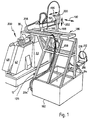
- Figure 1 shows a robotic system for handling circular platelike wafers of silicon typically 100 or 200mm diameter or larger
- Figures 1, 2 and 3 correspond to Figures 8 to 10 of our copending Patent Application reference C412/W.
- the system comprises a base 182 and structural framework generally designated 184 extending upwardly therefrom to provide a support for a linear slideway generally designated 186 along which a carriage 188 can slide in the direction of the arrow 190.
- a second slide 192 protrudes from the housing 188 at right angles to the slideway 186 and a sliding member 194 is adapted to move therealong in the direction of the arrow 196.
- An arm 198 protrudes from the housing 194 and a drive attached thereto and shown at 200 provides for movement of the arm 198 in the direction of the arrow 202.
- Electric power for the drives 200 and the drives in the housing 188 is provided via a multi-way umbilical 204 which is retained in the flexible safety harness 206 attached to the linear track 186.
- a vacuum chuck 208 At the lower end of the arm 198 is a vacuum chuck 208 and by suitable manoeuvring of the carriages 188 and 200 and the arm 198, so the vacuum chuck 208 can be positioned in front of a wafer 210 which is held upright in a supporting sleeve 212.
- An empty supporting sleeve at 214 is also shown ready to receive a processed wafer.
- a finished wafer workpiece 36 can be picked up from the workstation and to this end the transfer mechanism of Figure 1 is operated so as to position the chuck 208 opposite the wafer 36 on the workhead, so as to retrieve the finished wafer 36 and transfer this to the empty sleeve 214.
- Movement of the carriage 194 further out towards the sleeve 212 positions the chuck 208 in front of an unground workpiece 210, and after picking this up, it can be transferred into the inspection station and thereafter to the machining environment of the machine 400 for attachment to the vacuum chuck on the workhead in place of the previous wafer for grinding.
- a plurality of sleeves can be provided on the track 216 and all the workpieces located therein can be removed, centred, ground, inspected and returned thereto in turn.
- each of the wafers is positioned in the inspection apparatus shown in Figures 2 and 3, to enable the geometric centre of the wafer to be determined, and thereby allow it to be accurately positioned on the chuck 30 for grinding.
- the wafer may again be located for inspection of the edge profile of the wafer before it is returned to its storage sleeve.
- FIG 2 is an overall view showing where the inspection apparatus sits in relation to the grinding machine 400 and the robotic wafer handling system of Figure 1. As before the same reference numerals are used throughout.
- the inspection apparatus comprises a stand 218 on which is located a support framework which comprises a base 220 and an upright plate 222.
- a triangular stiffening plate 224 extends from the rear of the plate 222 and both 222 and 224 are welded to the plate 220 as at 226.
- a support bracket 230 Spaced from vertical edge 228 of the plate 222 is a support bracket 230, and a lamp and projection lens arrangement generally designated 232 is supported at the upper end of the bracket 230.
- a first camera 234 having a lens 236 is mounted on the plate 222 to view the edge of the disc 238 which is backlit by the lamp 232.
- a motor 240 is mounted on the rear of the plate 222.
- the motor drives a vacuum chuck on which the disc 238 which is to be inspected is planted by the vacuum chuck 208 of arm 198.
- Rotation of the motor 240 rotates the wafer 238.
- electrical signals can be derived from the camera output for feeding via a cable 242 to signal analysis apparatus for processing data obtained from the signals.
- a second camera 244 may be mounted on the support plate edge 228, with its optical axis tangential to the disc 238 (or at least parallel to the tangent thereto), to view the edge of the disc 238 generally tangentially, so as to obtain information on the profile of the edge.
- the disc edge is backlit by lamp 246 and signals from the camera 244 are supplied along cable 248. Power for the lamps 232 and 246 is supplied as required along cables 250 and 252 respectively.
- a computer 254 is supplied with signals from the camera 234 and via cables 242 and 248 and controls the cameras and their lamps 232 and 246 via return signal paths along 242 and 248 and via cables 250 and 252 respectively.
- the output of camera 244 can be displayed on a monitor 256 as required.
- the profile of the edge of the wafer 238 is shown at 258 together with a computer generated template 260, 262 showing eg the ideal angle for the sides of the profile.
- the shaded region 400 corresponds to the silhouette image of the disc 238 as seen by the CCD chip in the camera 234, where the disc has been rotated so that a notch 402 in its edge lies in the camera field of view.
- the shaded area 404 likewise corresponds to the silhouette image of the disc 238 as seen by the CCD chip, but this time with the notch out of the field of view of the camera.
- the notch only occupies a tiny percentage of the circumference of the disc, for the majority of the time the image presented to the camera chip will be as shown in Figure 5. However if the disc is mounted off-centre, the eccentric movement of the disc will cause the edge 406 of the shaded region to move over the surface of the CCD chip.
- the solid line 406 corresponds to the position of the image of the disc edge on the CCD chip in a position where the geometric centre of the disc has been rotated until it is displaced to the left of the axis about which the disc is being rotated, and the dotted outline 408 shows the position of the line 406 after the disc has rotated through 180°, so that the geometric centre (and therefore the image of the disc) has now shifted to the right.
- the shift H shown in Figure 5 is equal to twice the eccentricity of the disc where the eccentricity equals the distance between the centre of geometry of the disc and the centre about which the disc is being rotated.
- H H
- the geometric centre of the disc is co-incident with the axis about which the disc is rotated for machining purposes, or is displaced by a known amount along a given radius, relative to the machining axis, to accommodate a damaged region of the disc edge and allow regrinding of the disc.
- the present method and apparatus enables the geometric centre of the disc to be determined very accurately by noting the angular positions of the disc relative to the notch at which the various displacements of the image edge occur, and computing H (and therefore 1 ⁇ 2H).
- the edge of the disc is curved, the size of the CCD chip in the camera will be very small relative to the circumference of the disc, and although the line 406 has been shown as curved in Figure 5, the curvature will be barely visible in the image on the CCD chip and the .curvature in the drawing has been exaggerated. Provided the mechanism for moving the wafer and locating it on the workhead can do so very accurately, the accuracy with which the disc is located at the machining station will be dependent at least in part on the accuracy to which the dimension H can be measured.
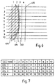
- the camera chip can be thought of as a rectilinear array of light sensitive devices closely packed and arranged in rows and columns.
- Figure 6 shows part of such an array and illustrates four of the columns and ten of the rows of such an array.
- the individual pixels contribute to the resolution in both the row and column direction and are made as small as possible.
- a camera chip having a diameter of approximately 1cm will have in excess of 100,000 such light sensitive elements (or pixels as they are commonly called), and it is not uncommon for the number of pixels to exceed 300,000 or more.
- the curvature of the line 412 in Figure 6 will be barely discernable relative to the matrix of rows and columns of pixels. However if we consider the curvature in the region of the notch for example the knuckle 414 in Figure 4, the curvature of the silhouette image in the region of the knuckle 414 might well equate to that shown in Figure 6.
- the mechanism of a CCD chip is such that at the beginning of each exposure period, all of the pixels are equally electrically charged.
- the array of pixels is then exposed to a pattern of light for a brief period of time and at the end of that period each of the pixels is inspected very rapidly and an electrical signal is generated for each of the pixels, the value of which is determined by the amount of charge needed to replace any which has dissipated during the exposure interval.
- the light sensitive elements are such that during the exposure period, if no light has fallen on a pixel, the charge at the end of the exposure period should be substantially the same as that at the beginning.
- the value of the electrical signal during read-out for such a pixel will therefore be high and might be digitised to a value 10.
- the original charge will be substantially dissipated and any light level above that threshold will not increase the electrical signal for that pixel during read-out. For this reason the quantity of light falling on the pixel array is controlled using an iris or neutral density filter and/or appropriate lighting, so that saturation as it is called does not occur. This means that the electrical signal value for each pixel during read-out will be proportional to the quantity of light which has fallen on the pixel during the exposure interval.
- the exposure interval is very short and the time to read out the pixels can be a tiny fraction of the exposure interval and typically a chip can be exposed and read out 50 times a second, although higher rates are possible.
- the electrical signal obtained during each read-out and generated by the electrical current needed to reinstate each pixel change can thus vary from 0 (for a pixel such as 1:1) to a maximum value '(say 10) for an unshaded pixel such as 3:1.
- a maximum value '(say 10) for an unshaded pixel such as 3:1.
- the amount of light falling thereon will be less than that of 3:1 and more than that of 1:1. If 50% of the pixel area is shaded, then approximately 50% of the light which would have produced a signal value of 10 on a read-out will have been received by the pixel during the exposure interval, and the digitised electrical signal value typically will be 5 when that pixel is read out.
- Figure 7 shows a table of typical digitised values of the electrical signal during read-out of the pixels in the array shown in Figure 6.
- the electrical signal from each read-out of the array must be interpreted so as to determine how far to the right the edge of the image has moved and therefore which of the columns has been intercepted. Since at the pixel level, the edge of the image may not be a sharp continuous line such as shown in Figure 6, and because of electrical imperfections and so-called electrical noise, low value signals can be obtained during read-out even from pixels which have been fully shaded, it is usually necessary to apply a so-called threshold to the signal value before a decision is taken as to whether or not the image of the disc edge has invaded a particular column of pixels or not.
- the maximum accuracy in the horizontal direction is therefore equal to the size of one pixel. Whilst this can be very small, it is nevertheless not necessarily accurate enough to allow the centre of the disc to be accurately located at the machining.
- a more accurate assessment of the position of the edge 414 can be made since if the actual digitised values are taken into account.
- the small change in value as between pixel 2:3 and pixel 3:3, is followed in column 4 by a pixel having a very low or zero value.
- the signal value in column 3 at row 3 can be considered to be a valid signal and can be taken into account.
- column 4 is the first column containing all high values and column 1 contains pixels all having zero or very low values and column 2 has generally low values in the region of the higher value signals in column 3.
- the precise position of the edge in for example row 4 can be said to be 20% across the width of pixel 3:4 measured from the left hand edge of the pixel.
- the digitised video signal values must therefore be considered in groups simultaneously and a decision taken to reject or allow through small changes for consideration depending on whether or not the small change is sandwiched between two low values or two high values, or in between a high and a low value. Only in the latter event would the intermediate signal value be retained for influencing the decision on the final position to be attributed to the disc edge.
- the tangential view of the edge profile should be as shown in Figure 9 where the shaded area 417 of the circular field of view is an idealised representation of the edge of the disc in silhouette.
- the edge profile of the disc is typically evaluated in person by the operator although automation may be possible.
- the image of the edge is not as shown in Figure 9, but is very obscure since the camera has to be located a considerable distance from the point on the periphery at which the optical axis intersects the disc edge, is to be brought into focus, and a considerable part of the edge of the disc (see 239 in Figure 10), will be in the field of view and will contribute to the image on the CCD chip.
- Telecentric lens such as supplied by Melles Griot of Cambridge, England, is used for the camera lens, it produces an in focus image to the same size of objects at different distances from the lens, and if the electrical signals from the camera are subjected to processing before they are used to generate a display on a visual display unit an image of the edge profile is obtained on the VDU which is sharp and clear, and unaffected by the presence of the disc between the region of interest and the camera.
- Hitachi KPM1 camera which has a chip which will allow a 768x576 pixel read out resolution.
- Figure 10 shows diagrammatically the signal processing and enhancement of the representation of the edge profile for display on a VDU display.
- the video signal is obtained by reading the pixels of the CCD chip of camera 244.
- the camera output is digitised and stored in a first frame store 420.
- the digital values in the frame store are processed by processor 420 using a computer programme stored in memory 424, and re-stored in a second frame store 426.
- a representation of the wafer edge in a computer VDU display is obtained by addressing the second frame store 426 via the computer bus 428 and video driver 430 for producing RGB signals for a VDU 432.
- the profile of the disc can be checked at a number of points around its circumference by rotating the disc between a number of stationary positions and exposing an image of the edge of the disc to the camera chip at each position and storing and processing the signal from each said stationary position of the disc.
- the camera may be operated so as to produce a video signal corresponding to each of a succession of images as the disc rotates continuously each image corresponding to the edge profile of a different region of the disc measured circularly around its circumference.
- the camera shutter may be operated in synchronism with the rotation of the disc to obtain this effect or the camera may be set to take a large number of high speed exposures as the disc rotates.
Landscapes
- Engineering & Computer Science (AREA)
- Mechanical Engineering (AREA)
- Physics & Mathematics (AREA)
- Condensed Matter Physics & Semiconductors (AREA)
- General Physics & Mathematics (AREA)
- Manufacturing & Machinery (AREA)
- Computer Hardware Design (AREA)
- Microelectronics & Electronic Packaging (AREA)
- Power Engineering (AREA)
- Inorganic Chemistry (AREA)
- Ceramic Engineering (AREA)
- Chemical & Material Sciences (AREA)
- Optics & Photonics (AREA)
- Mechanical Treatment Of Semiconductor (AREA)
- Grinding And Polishing Of Tertiary Curved Surfaces And Surfaces With Complex Shapes (AREA)
- Polishing Bodies And Polishing Tools (AREA)
- Constituent Portions Of Griding Lathes, Driving, Sensing And Control (AREA)
- Grinding Of Cylindrical And Plane Surfaces (AREA)
- Container, Conveyance, Adherence, Positioning, Of Wafer (AREA)
- Length Measuring Devices By Optical Means (AREA)
- Electrical Discharge Machining, Electrochemical Machining, And Combined Machining (AREA)
- Grinding-Machine Dressing And Accessory Apparatuses (AREA)
- Finish Polishing, Edge Sharpening, And Grinding By Specific Grinding Devices (AREA)
- Turning (AREA)
- Manipulator (AREA)
- Disintegrating Or Milling (AREA)
- Testing Or Measuring Of Semiconductors Or The Like (AREA)
Claims (18)
- Maschine zum Kantenschleifen von kreisförmigen Scheiben, z.B. Wafern, aus einem Material wie Silizium, in Verbindung mit einem optischen Überwachungssystem, das eine Kamera aufweist, deren Linse ein Bild der Kante der Scheibe in der Kamera ergibt, und mit einer Vorrichtung zum Beleuchten des Randbereiches der von der Kamera betrachteten Scheibe, wobei die Maschine eine Rechenvorrichtung zum Analysieren des Kamerabildes aufweist, um eine notwendige Bewegung der Scheibe zu ihrer Positionierung in eine korrekte Schleifposition zu bestimmen.
- Kombination nach Anspruch 1, bei der die Kamera eine CCD-Kamera ist, deren Linse ein optisches Bild der Kante der Scheibe auf dem CCD-Chip abbildet, wobei die Beleuchtungsvorrichtung den Randbereich der von der Kamera betrachteten Scheibe so beleuchtet, dass der von der Kamera betrachtete Randbereich von hinten beleuchtet wird und deshalb von der Kamera als Silhouette gesehen wird.
- Kombination nach Anspruch 2, bei der die CCD-Anordnung eine große Anzahl von adressierbaren Pixeln in einer rechteckigen Gruppierung enthält.
- Kombination nach Anspruch 2 oder 3, bei der die Rechenvorrichtung eine elektrische Schaltvorrichtung aufweist, die Signale aufnehmen kann, welche durch Abtasten der CCD-Anordnung erhalten werden, und die in der Lage ist, das Signal aus jedem adressierten Pixel in der CCD-Anordnung in einen digitalen Wert umzuwandeln, je nachdem, ob ein Pixel durch das Bild der Scheibenkante im Schatten liegt oder nicht.
- Kombination nach einem der Ansprüche 2 - 4, bei der für eine fest vorgegebene Anzahl von Pixeln der Grad der Digitalisierung eines jeden Pixel-Signalwertes die Genauigkeit des Überwachungssystems bestimmt.
- Kombination nach einem der Ansprüche 2 - 5, mit einer Vorrichtung zur Speicherung eines jeden Bildes nacheinander, eine Vorrichtung, durch die es möglich ist, pixelabhängige Signale von einem Bild zum nächsten zu vergleichen und ferner eine Vorrichtung, mit der aus diesem Vergleich jede Änderung im Wert des pixelabhängigen Signales von einem Bild zum nächsten bestimmt wird, damit ein Signal erzeugt wird, das eine Verschiebung in der Position des Bildes der Kante durch Bewegung der Kante der Scheibe in dem Betrachtungsfeld aufgrund einer exzentrischen Befestigung der Scheibe zur Drehung zustande bringt.
- Kombination nach Anspruch 6, bei der die Kante der Scheibe als ein Übergang zwischen hell und dunkel im Bild, das der CCD-Kamera präsentiert wird, erscheint und deshalb das pixelabhängige Signal sich von einem Extremwert in den anderen Extremwert, also zwischen Schatten und Nicht-Schatten verändert.
- Kombination nach Anspruch 7, bei der die Pixel-Signale auf einer Skala von n=A entsprechend einer voll abgedunkelten oder schwarzen Stelle auf n = B, wobei B einer Nicht-Abdunkelung entspricht, digitalisiert werden, eine digitale Analyse durchgeführt wird, um exakter zu bestimmen, wo die Kante des Scheibenbildes in bezug auf die Pixel liegt, wobei dann, wenn zufällig ein Pixel durchschnitten wird, der jeweilige Wert von n, der einem geschnittenen Pixel auf der Skala A→B zugeschrieben wird, den prozentualen Anteil des Pixels, der von dem Scheibenbild bedeckt und deshalb abgedunkelt ist, und den prozentualen Anteil, der nicht abgedunkelt ist, anzeigt.
- Kombination nach Anspruch 8, bei der die Pixel-Auflösung so ausgelegt ist, dass eine "Kante" in den Werten einer Anzahl von anschließenden Pixeln "gesehen" werden kann, eine Vorrichtung vorgesehen ist, mit der Signale entsprechend den Pixeln in Gruppen gleichzeitig abgefragt werden können, eine Impuls-Auswählvorrichtung einzelne "vagabundierende" Werte identifiziert, die unter anderem dem Rauschen usw. zugeschrieben werden und diese aus dem Signal entfernt werden und eine Vorrichtung zur Bestimmung der echten Kante vorgesehen ist, die dort gesehen wird, wo eine Mehrzahl der anschließenden Pixel-Signalwerte dies anzeigen.
- Kombination nach einem der Ansprüche 2 - 9, bei der jede Fehlausrichtung der in Rotation versetzten Scheibe zwischen dem geometrischen Mittelpunkt der Scheibe und ihrer Rotationsachse in der Überwachungsstation als eine Verschiebung des Bildes der Scheibe auf der CCD erscheint.
- Kombination nach Anspruch 10, mit einer Vorrichtung zur Speicherung des Wertes der Verschiebung bei einer Vielzahl von im Winkel versetzten Positionen, die durch den Codierer bestimmt werden, und einer Vorrichtung zum Berechnen der X Z Koordinaten (X1 Z1) des geometrischen Mittelpunktes der Scheibe daraus.
- Kombination nach einem der Ansprüche 2 - 11, bei der eine zweite Kamera so positioniert ist, dass sie den Rand der Scheibe tangential betrachtet, wobei die optische Achse der Kamera in oder parallel zur Ebene der Scheibe liegt, um das Profil der Kante der Scheibe in einem vergrößerten Maßstab überwachen zu können, indem ein vergrößertes Bild des optischen, von der Kamera auf einer CRT-Röhre geliefertes Bild dargestellt wird.
- Kombination nach Anspruch 12, bei der die zweite Kamera eine telezentrische Linse aufweist, die ein im Brennpunkt liegendes Bild mit der gleichen Größe von Objekten über einen Bereich von Abständen von der Linse erzeugt.
- Kombination nach Anspruch 13, mit einer CCD-Kamera in Verbindung mit einer telezentrischen Linse zum Digitalisieren des Videosignals aus der Kamera, und mit einer Signalverarbeitungsvorrichtung zur Erzeugung eines Signals für die Sichtanzeige auf einem Rechnermonitor.
- Kombination nach einem der Ansprüche 1 - 14, bei der die Maschine ein Ausricht- und Verschiebesystem zum Bewegen kreisförmiger Scheiben-Werkstücke von einer ersten Überwachungsstation in eine zweite Bearbeitungsstation aufweist, dieses System eine Werkstück-Haltevorrichtung zur Befestigung mit der Stirnseite eines Scheiben-Werkstückes besitzt, um letzteres von einer Position in eine andere Position zu bewegen, mit einem Roboter, der die Position der Werkstück-Haltevorrichtung steuert und in der Lage ist, Bewegungen in mindestens zwei zueinander rechtwinkligen Richtungen auszuführen, die beide parallel zu der Ebene der Scheibe liegen, wenn sie die erste Station einnimmt und mit einer Vorrichtung zum Rotieren der Scheibe in der Überwachtungsstation und in der Bearbeitungsstation, während die Überwachungsstation zur Bestimmung der Position des geometrischen Mittelpunktes der Scheibe bei deren Rotation in der ersten Station dient, und die Rechenvorrichtung aus von der Überwachungsvor-richtung gelieferten Daten alle Verschiebungen berechnet, die längs der ortho-gonalen Bewegungsrichtungen des Roboters erforderlich sind, um den geometri-schen Mittelpunkt der Scheibe in eine zweite gewünschte Position, deren Koordinaten bekannt sind, zu bewegen.
- Kombination nach Anspruch 15, bei der ein kreisförmiger Wafer, der zum Kantenschleifen in der Überwachungsstation so platziert wird, dass sein geometrischer Mittelpunkt etwa mit der Rotationsachse der Überwachungsstation ausgerichtet ist, um die Achse der Überwachungsstation gedreht wird, und die Rechenvorrichtung zur Bestimmung zweier Dimensionen X1 und Z1, nämlich der Abstände gemessen parallel zu den X- und Z-Achsen, dient, um die die geometrische Mitte des Wafers verschoben werden muss, damit sie mit der Rotationsmitte der Übertragungsstation zusammenfällt, und die Maschine eine Schleif-Spannvorrichtung aufweist, auf die der Wafer mit Hilfe des Roboters übertragen und darauf positioniert wird, indem Kompensationen in den X- und Z-Richtungen vorgenommen werden, damit der nunmehr bekannte geometrische Mittelpunkt des Wafers exakt in bezug auf die Rotationsachse der Schleif-Spannvorrichtung positioniert wird.
- Kombination nach Anspruch 16, bei der dann, wenn eine Beschädigung am Umfang eines Wafers auftritt, der Wafer absichtlich exzentrisch auf der Spannvorrichtung der Schleifstation angeordnet wird, so dass bei Vorhandensein einer Beschädigung am Umfang der Wafer erneut um einen neuen Mittelpunkt geschliffen wird, damit der unerwünschte, beschädigte Umfangsbereich entfernt wird.
- Kombination nach Anspruch 16, bei der die optische Überwachungsvorrichtung auf der Überwachungsstation angeordnet ist, wobei die optische Achse parallel zu der Y-Achse, d.h. der Rotationsachse des Werkstückes in der Überwachungsstation verläuft.
Applications Claiming Priority (7)
| Application Number | Priority Date | Filing Date | Title |
|---|---|---|---|
| GB9612594 | 1996-06-15 | ||
| GBGB9612594.3A GB9612594D0 (en) | 1996-06-15 | 1996-06-15 | Improvements in and relating to grinding machines |
| GB9626397 | 1996-12-19 | ||
| GBGB9626415.5A GB9626415D0 (en) | 1996-12-19 | 1996-12-19 | Workpiece inspection and handling |
| GB9626415 | 1996-12-19 | ||
| GBGB9626397.5A GB9626397D0 (en) | 1996-12-19 | 1996-12-19 | Improvements in and relating to grinding and polishing machines |
| PCT/GB1997/001570 WO1997048525A1 (en) | 1996-06-15 | 1997-06-11 | Workpiece inspection and handling |
Publications (2)
| Publication Number | Publication Date |
|---|---|
| EP0906174A1 EP0906174A1 (de) | 1999-04-07 |
| EP0906174B1 true EP0906174B1 (de) | 2002-08-28 |
Family
ID=27268329
Family Applications (9)
| Application Number | Title | Priority Date | Filing Date |
|---|---|---|---|
| EP97925191A Expired - Lifetime EP0865342B1 (de) | 1996-06-15 | 1997-06-11 | Verfahren zum schleifen von kanten |
| EP00114717A Withdrawn EP1050370A3 (de) | 1996-06-15 | 1997-06-11 | Schleifmaschine mit kurzem versteifenden Verbindungsaufbau |
| EP00102819A Expired - Lifetime EP1005955B1 (de) | 1996-06-15 | 1997-06-11 | Flexible Verbindung einer Schleifmaschinenspindel zu einer Plattform |
| EP97925193A Expired - Lifetime EP0906174B1 (de) | 1996-06-15 | 1997-06-11 | Werkstückinspektion und handhabung |
| EP97925192A Expired - Lifetime EP0907461B1 (de) | 1996-06-15 | 1997-06-11 | Flexible verbindung einer schleifmaschinenspindel zu einer plattform |
| EP00102837A Expired - Lifetime EP1005956B1 (de) | 1996-06-15 | 1997-06-11 | Flexible Verbindung einer Schleifmaschinenspindel zu einer Plattform |
| EP00102823A Expired - Lifetime EP1000706B1 (de) | 1996-06-15 | 1997-06-11 | Flexible verbindung einer schleifmaschinenspindel zu einer plattform |
| EP00114816A Withdrawn EP1048403A3 (de) | 1996-06-15 | 1997-06-11 | Verbesserungen an/und im Zusammenhang mit Schleifmaschinen |
| EP98309186A Withdrawn EP0904893A3 (de) | 1996-06-15 | 1997-06-11 | Inspektion der Kante einer Halbleiterscheibe nach dem Schleifen |
Family Applications Before (3)
| Application Number | Title | Priority Date | Filing Date |
|---|---|---|---|
| EP97925191A Expired - Lifetime EP0865342B1 (de) | 1996-06-15 | 1997-06-11 | Verfahren zum schleifen von kanten |
| EP00114717A Withdrawn EP1050370A3 (de) | 1996-06-15 | 1997-06-11 | Schleifmaschine mit kurzem versteifenden Verbindungsaufbau |
| EP00102819A Expired - Lifetime EP1005955B1 (de) | 1996-06-15 | 1997-06-11 | Flexible Verbindung einer Schleifmaschinenspindel zu einer Plattform |
Family Applications After (5)
| Application Number | Title | Priority Date | Filing Date |
|---|---|---|---|
| EP97925192A Expired - Lifetime EP0907461B1 (de) | 1996-06-15 | 1997-06-11 | Flexible verbindung einer schleifmaschinenspindel zu einer plattform |
| EP00102837A Expired - Lifetime EP1005956B1 (de) | 1996-06-15 | 1997-06-11 | Flexible Verbindung einer Schleifmaschinenspindel zu einer Plattform |
| EP00102823A Expired - Lifetime EP1000706B1 (de) | 1996-06-15 | 1997-06-11 | Flexible verbindung einer schleifmaschinenspindel zu einer plattform |
| EP00114816A Withdrawn EP1048403A3 (de) | 1996-06-15 | 1997-06-11 | Verbesserungen an/und im Zusammenhang mit Schleifmaschinen |
| EP98309186A Withdrawn EP0904893A3 (de) | 1996-06-15 | 1997-06-11 | Inspektion der Kante einer Halbleiterscheibe nach dem Schleifen |
Country Status (13)
| Country | Link |
|---|---|
| US (5) | US6224459B1 (de) |
| EP (9) | EP0865342B1 (de) |
| JP (6) | JP2000512564A (de) |
| KR (4) | KR100303074B1 (de) |
| CN (4) | CN1082868C (de) |
| AT (6) | ATE214321T1 (de) |
| AU (3) | AU3042097A (de) |
| DE (6) | DE69709924D1 (de) |
| ES (4) | ES2211390T3 (de) |
| GB (2) | GB2314037B (de) |
| MY (3) | MY132625A (de) |
| TW (3) | TW434117B (de) |
| WO (3) | WO1997048526A1 (de) |
Families Citing this family (102)
| Publication number | Priority date | Publication date | Assignee | Title |
|---|---|---|---|---|
| DE69709924D1 (de) * | 1996-06-15 | 2002-02-28 | Unova Uk Ltd | Flexible verbindung einer schleifmaschinenspindel zu einer plattform |
| DE945216T1 (de) * | 1998-03-25 | 2000-06-08 | Unova Uk Ltd | Kerben-Schleifwerkzeug |
| US6190261B1 (en) * | 1998-09-15 | 2001-02-20 | Flowserve Management Company | Pump assembly shaft guard |
| JP2000254857A (ja) * | 1999-01-06 | 2000-09-19 | Tokyo Seimitsu Co Ltd | 平面加工装置及び平面加工方法 |
| US6690473B1 (en) | 1999-02-01 | 2004-02-10 | Sensys Instruments Corporation | Integrated surface metrology |
| US7177019B2 (en) | 1999-02-01 | 2007-02-13 | Tokyo Electron Limited | Apparatus for imaging metrology |
| US7042580B1 (en) | 1999-02-01 | 2006-05-09 | Tokyo Electron Limited | Apparatus for imaging metrology |
| US6563586B1 (en) | 1999-02-01 | 2003-05-13 | Therma-Wave, Inc. | Wafer metrology apparatus and method |
| DE19910747B9 (de) * | 1999-03-11 | 2012-03-08 | Reishauer Ag | Verfahren und Vorrichtung zum Einmitten eines Abrichtwerkzeuges in die Ganglücke einer Schleifschnecke |
| AU4175800A (en) * | 1999-03-22 | 2000-10-09 | Sensys Instruments Corporation | Method and apparatus for wafer metrology |
| GB2351684B (en) * | 1999-07-03 | 2001-07-11 | Unova Uk Ltd | Improvement in and relating to edge grinding |
| MY126790A (en) * | 1999-09-16 | 2006-10-31 | Neomax Co Ltd | Method and apparatus for grinding magnetic member and method and apparatus for treating waste fluid |
| US6645059B1 (en) * | 1999-12-01 | 2003-11-11 | Gerber Coburn Optical Inc. | Device for retaining abrasive pad on lap in eyeglass lens making apparatus |
| GB0002251D0 (en) * | 2000-02-02 | 2000-03-22 | Unova Uk Ltd | Improvements in and relating to grinding machines |
| US6852012B2 (en) * | 2000-03-17 | 2005-02-08 | Wafer Solutions, Inc. | Cluster tool systems and methods for in fab wafer processing |
| DE10059067A1 (de) * | 2000-11-28 | 2002-06-06 | Peter Baeumler | Verfahren und Vorrichtung zur Herstellung von Zahnriemenformen und Zahnrädern |
| US6672943B2 (en) | 2001-01-26 | 2004-01-06 | Wafer Solutions, Inc. | Eccentric abrasive wheel for wafer processing |
| US6443817B1 (en) * | 2001-02-06 | 2002-09-03 | Mccarter Technology, Inc. | Method of finishing a silicon part |
| US6632012B2 (en) | 2001-03-30 | 2003-10-14 | Wafer Solutions, Inc. | Mixing manifold for multiple inlet chemistry fluids |
| ITBO20010434A1 (it) * | 2001-07-11 | 2003-01-11 | Marposs Spa | Apparecchiatura e metodo per il controllo del processo di lavorazionedi una macchina utensile |
| AT412197B (de) * | 2002-11-22 | 2004-11-25 | Lisec Peter | Vorrichtung zum bearbeiten von werkstoffplatten |
| KR100832297B1 (ko) * | 2002-12-17 | 2008-05-26 | 엘지디스플레이 주식회사 | 액정 표시패널의 연마량 측정장치 및 측정방법 |
| US6921322B2 (en) * | 2003-01-24 | 2005-07-26 | Artisan Industries, Inc. | Apparatus and methods for refinishing a surface in-situ |
| DE10303459A1 (de) * | 2003-01-29 | 2004-08-19 | Infineon Technologies Ag | Verfahren und Vorrichtung zum Kontrollieren des Randes eines scheibenförmigen Gegenstandes |
| US20050036717A1 (en) * | 2003-03-05 | 2005-02-17 | Tilia International, Inc. | Sealable bag having an integrated zipper for use in vacuum packaging |
| AU2003283553A1 (en) * | 2003-04-01 | 2004-10-25 | Unova U.K. Limited | Workpiece cooling during grinding |
| KR100940431B1 (ko) * | 2003-06-20 | 2010-02-10 | 주식회사 포스코 | 드라이어 공정의 스와프 제거 장치 |
| US7354990B2 (en) | 2003-08-26 | 2008-04-08 | General Electric Company | Purified polymeric materials and methods of purifying polymeric materials |
| US7244813B2 (en) * | 2003-08-26 | 2007-07-17 | General Electric Company | Methods of purifying polymeric material |
| JP4481667B2 (ja) * | 2004-02-02 | 2010-06-16 | 株式会社ディスコ | 切削方法 |
| EP1645513A3 (de) * | 2004-09-21 | 2006-04-19 | Philip Morris Products S.A. | Modulares Verpackungssystem |
| KR100573035B1 (ko) | 2004-09-24 | 2006-04-24 | 주식회사 실트론 | 웨이퍼 성형장치와 이 장치를 이용한 성형 방법 |
| CN100386179C (zh) * | 2005-05-24 | 2008-05-07 | 亚洲光学股份有限公司 | 重置定心系统 |
| CA2571275A1 (en) * | 2005-12-15 | 2007-06-15 | Ingersoll Machine Tools, Inc. | Determining cutting tool dimensions and run-out using acoustic emissions |
| CN100404200C (zh) * | 2006-04-14 | 2008-07-23 | 柯明月 | 硬脆材料颗粒产品表面磨削抛光机床 |
| KR100718943B1 (ko) * | 2006-05-29 | 2007-05-16 | 한국생산기술연구원 | 자석을 이용한 조립 장치 및 방법 |
| JP4915146B2 (ja) * | 2006-06-08 | 2012-04-11 | 信越半導体株式会社 | ウェーハの製造方法 |
| DE102006037267B4 (de) * | 2006-08-09 | 2010-12-09 | Siltronic Ag | Verfahren zur Herstellung von Halbleiterscheiben mit hochpräzisem Kantenprofil |
| JP4862896B2 (ja) * | 2007-01-31 | 2012-01-25 | 信越半導体株式会社 | シリコンウエーハの面取り装置およびシリコンウエーハの製造方法ならびにエッチドシリコンウエーハ |
| US20080252726A1 (en) * | 2007-04-10 | 2008-10-16 | Eastway Fair Company Limited | Video aid system |
| US7925075B2 (en) * | 2007-05-07 | 2011-04-12 | General Electric Company | Inspection system and methods with autocompensation for edge break gauging orientation |
| JP4999560B2 (ja) * | 2007-06-07 | 2012-08-15 | 豊田バンモップス株式会社 | 研削盤における砥石軸装置 |
| JP4262285B2 (ja) * | 2007-07-18 | 2009-05-13 | 株式会社コベルコ科研 | 形状測定装置,形状測定方法 |
| KR20090063804A (ko) | 2007-12-14 | 2009-06-18 | 주식회사 실트론 | 연삭 휠 트루잉 공구 및 그 제작방법, 이를 이용한 트루잉장치, 연삭 휠의 제작방법, 및 웨이퍼 에지 연삭장치 |
| WO2009094539A1 (en) * | 2008-01-24 | 2009-07-30 | Applied Materials, Inc. | Solar panel edge deletion module |
| JP5270974B2 (ja) * | 2008-06-17 | 2013-08-21 | 中村留精密工業株式会社 | 基板端面の研磨装置及び研磨判定方法 |
| JP5160993B2 (ja) * | 2008-07-25 | 2013-03-13 | 株式会社荏原製作所 | 基板処理装置 |
| JP4734398B2 (ja) * | 2008-12-04 | 2011-07-27 | 株式会社コベルコ科研 | 形状測定装置,形状測定方法 |
| JP2010162624A (ja) * | 2009-01-13 | 2010-07-29 | Ebara Corp | 研磨装置および研磨方法 |
| JP5328025B2 (ja) * | 2009-02-24 | 2013-10-30 | 株式会社和井田製作所 | エッジ検出装置及びこれを用いた工作機械、エッジ検出方法 |
| DE102009023275A1 (de) * | 2009-05-29 | 2010-12-02 | Liebherr-Verzahntechnik Gmbh | Verzahnmaschine |
| JP5471055B2 (ja) * | 2009-06-15 | 2014-04-16 | 株式会社ジェイテクト | 砥石の成形方法及び研削盤 |
| JP5621276B2 (ja) * | 2010-03-01 | 2014-11-12 | セイコーエプソン株式会社 | 液滴吐出装置 |
| TWM383466U (en) * | 2010-03-02 | 2010-07-01 | Axisco Prec Machinery Co Ltd | High-efficiency fine & coarse grinding CNC dual-axes surface grinder |
| CN101870088B (zh) * | 2010-06-13 | 2012-07-04 | 北京航空航天大学 | 用于端面磨削的密闭供液自吸式内冷却砂轮装置 |
| EP2433747B1 (de) * | 2010-09-24 | 2013-04-17 | Benteler Maschinenbau GmbH | Verfahren und Vorrichtung zum Schleifen der parallel zueinander verlaufenden Kanten von Glasplatten |
| US8629902B2 (en) * | 2010-10-12 | 2014-01-14 | Kla-Tencor Corporation | Coordinate fusion and thickness calibration for semiconductor wafer edge inspection |
| CN103442843B (zh) * | 2011-03-24 | 2016-04-20 | 埃尔温容克尔机械制造有限公司 | 磨削机装置和用于枢转磨削主轴单元的方法 |
| US20130057693A1 (en) * | 2011-09-02 | 2013-03-07 | John Baranek | Intruder imaging and identification system |
| US20130196572A1 (en) * | 2012-01-27 | 2013-08-01 | Sen-Hou Ko | Conditioning a pad in a cleaning module |
| CN102848309A (zh) * | 2012-10-08 | 2013-01-02 | 江苏环洋组合机床有限公司 | 一种活塞环内外角磨床磨头组件 |
| US9254549B2 (en) * | 2013-05-07 | 2016-02-09 | Jtekt Corporation | Grinding machine |
| TWI600499B (zh) * | 2013-08-09 | 2017-10-01 | Nakamura-Tome Precision Industry Co Ltd | Hard brittle plate grinding device and processing precision measurement and correction method |
| KR101531820B1 (ko) * | 2013-10-16 | 2015-06-24 | 서우테크놀로지 주식회사 | 반도체 스트립 그라인더 |
| TWI695441B (zh) * | 2013-12-02 | 2020-06-01 | 日商大亨股份有限公司 | 工件處理裝置、工件輸送系統 |
| US9886029B2 (en) * | 2013-12-02 | 2018-02-06 | Daihen Corporation | Workpiece processing apparatus and workpiece transfer system |
| US9498865B2 (en) * | 2013-12-27 | 2016-11-22 | United Technologies Corporation | System and methods for rough grinding |
| CN104748676A (zh) * | 2013-12-31 | 2015-07-01 | 北京北方微电子基地设备工艺研究中心有限责任公司 | 位置检测装置和传输系统 |
| DE202015001082U1 (de) * | 2015-02-06 | 2015-02-24 | Deckel Maho Pfronten Gmbh | Spindelvorrichtung für eine programmgesteuerte Werkzeugmaschine |
| CN105171701A (zh) * | 2015-07-20 | 2015-12-23 | 中国科学院上海光学精密机械研究所 | 高洁净真空位移台 |
| CN105345605A (zh) * | 2015-09-25 | 2016-02-24 | 广东先导半导体材料有限公司 | 一种晶片磨边方法和磨边机吸盘 |
| JP6555587B2 (ja) * | 2015-10-28 | 2019-08-07 | 日本電気硝子株式会社 | 板ガラスの製造方法及び製造装置 |
| KR102214510B1 (ko) * | 2016-01-18 | 2021-02-09 | 삼성전자 주식회사 | 기판 씨닝 장치, 이를 이용한 기판의 씨닝 방법, 및 반도체 패키지의 제조 방법 |
| JP6321703B2 (ja) * | 2016-03-04 | 2018-05-09 | ファナック株式会社 | ワイヤ放電加工機の検査システム |
| CN107283273B (zh) * | 2016-04-06 | 2023-08-01 | 天通日进精密技术有限公司 | 晶棒加工设备及用于该设备的主轴机构与晶棒加工方法 |
| CN107303650A (zh) * | 2016-04-21 | 2017-10-31 | 广东罗庚机器人有限公司 | 用于打磨抛光的自动抓取方法、装置及系统 |
| JP6651636B2 (ja) * | 2016-08-30 | 2020-02-19 | 本田技研工業株式会社 | ロボットの制御装置およびロボットの制御方法 |
| JP6912794B2 (ja) * | 2016-10-26 | 2021-08-04 | 株式会社シギヤ精機製作所 | 研削盤 |
| CN109937107A (zh) * | 2016-11-08 | 2019-06-25 | 贝瓦克生产机械有限公司 | 用于修整罐的方法和设备 |
| CN107081647B (zh) * | 2017-05-16 | 2023-04-11 | 四川纽赛特工业机器人制造有限公司 | 一种机器人打磨标准站 |
| CN108972263A (zh) * | 2017-06-02 | 2018-12-11 | 美克国际家私加工(天津)有限公司 | 一种多功能砂光工作站 |
| US10661406B2 (en) | 2018-01-11 | 2020-05-26 | Razor Edge Systems, Inc. | Robotic hand tool sharpening and cleaning apparatus |
| DE102018104550B4 (de) * | 2018-02-28 | 2022-10-13 | Walter Maschinenbau Gmbh | Werkzeugmaschine, insbesondere Schleif- und/oder Erodiermaschine sowie Verfahren zum Auswechseln einer Werkzeugbaugruppe |
| CN110549201B (zh) * | 2018-05-31 | 2023-01-17 | 长濑因特格莱斯株式会社 | 机床 |
| CN108747825B (zh) * | 2018-06-19 | 2020-04-21 | 湖南大学 | 一种基于视觉检测激光修整成型砂轮装置及其修整方法 |
| CN108714854B (zh) * | 2018-06-19 | 2020-09-11 | 湖南镭盛机电科技有限公司 | 基于复映法的成形砂轮检测修整装置及砂轮整形方法 |
| CN108747632A (zh) * | 2018-07-06 | 2018-11-06 | 湖州吉弘机械有限公司 | 一种叉车铸件生产打磨装置 |
| US10835920B2 (en) * | 2018-08-03 | 2020-11-17 | Indian Institute Of Technology Ropar | Technology and process for coating a substrate with swarf particles |
| EP3608060A1 (de) * | 2018-08-07 | 2020-02-12 | Comadur S.A. | Bearbeitungswerkzeug zum schleifen eines werkstücks |
| KR101966017B1 (ko) * | 2018-09-13 | 2019-04-04 | 오민섭 | 반도체소자의 불량분석을 위한 그라인딩 제어 방법 및 장치 |
| CN109839077B (zh) * | 2018-12-26 | 2020-10-13 | 太原理工大学 | 一种基于断面轮廓序列的微观多相结构三维建模测量装置 |
| CN109746786A (zh) * | 2019-01-22 | 2019-05-14 | 安徽鑫艺达抛光机械有限公司 | 一种半罐打磨装置 |
| US11577365B2 (en) | 2019-04-05 | 2023-02-14 | Honda Motor Co., Ltd. | Systems and methods of processing a rotatable assembly |
| CN109968147A (zh) * | 2019-04-15 | 2019-07-05 | 天津中屹铭科技有限公司 | 一种触觉高刚性可操控加工机器人 |
| CN112336295A (zh) * | 2019-08-08 | 2021-02-09 | 上海安翰医疗技术有限公司 | 磁性胶囊内窥镜的控制方法、装置、存储介质、电子装置 |
| KR102381559B1 (ko) * | 2019-10-29 | 2022-04-04 | (주)미래컴퍼니 | 연마 시스템 |
| TWM597200U (zh) * | 2020-02-18 | 2020-06-21 | 財團法人金屬工業研究發展中心 | 研磨輪量測裝置 |
| CN112809499B (zh) * | 2020-12-31 | 2022-03-29 | 开平市伟利卫浴有限公司 | 一种自冷却降温的打磨机 |
| CN113523903B (zh) * | 2021-07-27 | 2022-05-13 | 山东亿佰通机械股份有限公司 | 一种可调节的阀门加工平台 |
| CN115091224B (zh) * | 2022-08-05 | 2024-05-10 | 上海交通大学 | 用于薄壁件镜像铣削的射流主动抑振装置及方法 |
| CN115008302A (zh) * | 2022-08-10 | 2022-09-06 | 江苏二马液压元件有限公司 | 一种安全阀加工用密封面研磨装置 |
| CN117207063B (zh) * | 2023-11-07 | 2024-01-30 | 江苏阔能建材科技有限公司 | 一种用于特种门窗加工的打磨头以及智能磨床 |
Family Cites Families (42)
| Publication number | Priority date | Publication date | Assignee | Title |
|---|---|---|---|---|
| GB684933A (en) * | 1951-02-15 | 1952-12-24 | Timken Roller Bearing Co | Improvements in continuous feed reed-type honing machines |
| US2680941A (en) * | 1951-06-26 | 1954-06-15 | Heald Machine Co | Internal grinding machine |
| GB885062A (en) * | 1958-07-10 | 1961-12-20 | Jones & Shipman A A Ltd | Improvements relating to the machining of workpieces in grinding machines |
| US3361018A (en) * | 1965-10-08 | 1968-01-02 | Elihu I. Druckman | Spring mounted tool holder |
| US3534502A (en) * | 1968-01-24 | 1970-10-20 | Bryant Grinder Corp | Apparatus and method for grinding an external surface of revolution |
| GB1430632A (en) * | 1972-05-03 | 1976-03-31 | Schiess Ag | Grinding machines |
| GB1551923A (en) * | 1975-09-18 | 1979-09-05 | Toyoda Machine Works Ltd | Feed apparatus in a grinding-machine |
| DE3030914C2 (de) * | 1980-08-16 | 1989-08-10 | Peter 6000 Frankfurt Koblischek | Verfahren zur Herstellung von Maschinenständern mittels Polymerbeton |
| CH653941A5 (de) * | 1980-12-13 | 1986-01-31 | Hauni Werke Koerber & Co Kg | Vorrichtung zum umspannen planparalleler werkstuecke. |
| DE3114078A1 (de) * | 1981-04-08 | 1982-11-04 | Löhr & Herrmann Ingenieurgesellschaft mbH, 7531 Neuhausen | Vorrichtung zum kantenschleifen von plattenfoermigem gut |
| DE3204987C2 (de) * | 1982-02-12 | 1986-06-05 | Supfina Maschinenfabrik Hentzen GmbH & Co KG, 5630 Remscheid | Spannvorrichtung für durchmesserkleine scheibenförmige Werkstücke |
| JPS60104644A (ja) * | 1983-11-08 | 1985-06-10 | Mitsubishi Metal Corp | ウエハ−の外周研削・面取装置 |
| GB2157078B (en) * | 1984-03-30 | 1987-09-30 | Perkin Elmer Corp | Wafer alignment apparatus |
| SU1252136A1 (ru) * | 1984-07-31 | 1986-08-23 | Ордена Трудового Красного Знамени Институт Сверхтвердых Материалов Ан Усср | Устройство дл обработки плоских поверхностей |
| US4607461A (en) * | 1984-12-10 | 1986-08-26 | Charles Adams | Accurate positioning apparatus |
| US4638601A (en) * | 1985-11-04 | 1987-01-27 | Silicon Technology Corporation | Automatic edge grinder |
| US4794736A (en) * | 1985-12-27 | 1989-01-03 | Citizen Watch Co., Ltd. | Arrangement for mechanically and accurately processing a workpiece with a position detecting pattern or patterns |
| JPS6322259A (ja) * | 1986-07-10 | 1988-01-29 | Hitachi Cable Ltd | 半導体ウエハ加工方法および加工装置 |
| GB8701616D0 (en) * | 1987-01-26 | 1987-03-04 | Michell Instr Ltd | Dewpoint meter |
| JPH0637025B2 (ja) * | 1987-09-14 | 1994-05-18 | スピードファム株式会社 | ウエハの鏡面加工装置 |
| US4953522A (en) * | 1987-11-27 | 1990-09-04 | Schaudt Maschinenbau Gmbh | Method of dressing grinding wheels in grinding machines |
| JPH06104297B2 (ja) * | 1989-04-27 | 1994-12-21 | 信越半導体株式会社 | 半導体ウエーハの面取り装置 |
| US5201145A (en) * | 1990-03-31 | 1993-04-13 | Shin-Etsu Handotai Company, Limited | Monocrystal ingot attitude-adjusting/surface-grinding/conveying apparatus |
| US5185965A (en) * | 1991-07-12 | 1993-02-16 | Daito Shoji Co., Ltd. | Method and apparatus for grinding notches of semiconductor wafer |
| KR0185234B1 (ko) * | 1991-11-28 | 1999-04-15 | 가부시키 가이샤 토쿄 세이미쯔 | 반도체 웨이퍼의 모떼기 방법 |
| JP2760918B2 (ja) * | 1992-02-03 | 1998-06-04 | 大日本スクリーン製造株式会社 | ノッチ付ウエハの位置検出装置 |
| FR2691663B1 (fr) * | 1992-05-26 | 1996-10-11 | Essilor Int | Procede de ravivage de meules, disque et machine pour sa mise en óoeuvre. |
| DE4222790C1 (de) * | 1992-07-10 | 1994-01-05 | Netzsch Erich Holding | Verfahren und Anlage zum Entgraten und Weiterbearbeiten von Werkstücken, insbesondere aus keramischem Material |
| US5289661A (en) * | 1992-12-23 | 1994-03-01 | Texas Instruments Incorporated | Notch beveling on semiconductor wafer edges |
| DE4320934C2 (de) * | 1993-06-24 | 1995-04-20 | Wernicke & Co Gmbh | Brillenglasrandschleifmaschine |
| DE9313220U1 (de) * | 1993-09-02 | 1993-11-18 | Metabowerke Kg | Bandschleifmaschine |
| JPH07205001A (ja) * | 1993-11-16 | 1995-08-08 | Tokyo Seimitsu Co Ltd | ウェーハ面取り機 |
| IT1262263B (it) * | 1993-12-30 | 1996-06-19 | Delle Vedove Levigatrici Spa | Procedimento di levigatura per profili curvi e sagomati e macchina levigatrice che realizza tale procedimento |
| JP3035690B2 (ja) * | 1994-01-27 | 2000-04-24 | 株式会社東京精密 | ウェーハ直径・断面形状測定装置及びそれを組み込んだウェーハ面取り機 |
| US5452521A (en) * | 1994-03-09 | 1995-09-26 | Niewmierzycki; Leszek | Workpiece alignment structure and method |
| DE4414784C2 (de) * | 1994-04-28 | 1996-07-18 | Wernicke & Co Gmbh | Anlage zum Schleifen des Umfangsrandes und/ oder einer optischen Oberfläche von Brillengläsern |
| US5679060A (en) * | 1994-07-14 | 1997-10-21 | Silicon Technology Corporation | Wafer grinding machine |
| JP3010572B2 (ja) * | 1994-09-29 | 2000-02-21 | 株式会社東京精密 | ウェーハエッジの加工装置 |
| US5595528A (en) * | 1994-10-19 | 1997-01-21 | Vermont Rebuild, Inc. | Grinding wheel dresser |
| JP2882458B2 (ja) * | 1994-11-28 | 1999-04-12 | 株式会社東京精密 | ウェーハ面取り機 |
| JPH08243891A (ja) * | 1995-03-07 | 1996-09-24 | Kao Corp | 基板のチャンファ加工装置 |
| DE69709924D1 (de) * | 1996-06-15 | 2002-02-28 | Unova Uk Ltd | Flexible verbindung einer schleifmaschinenspindel zu einer plattform |
-
1997
- 1997-06-11 DE DE69709924T patent/DE69709924D1/de not_active Expired - Fee Related
- 1997-06-11 DE DE69723881T patent/DE69723881T2/de not_active Expired - Fee Related
- 1997-06-11 DE DE69738673T patent/DE69738673D1/de not_active Expired - Fee Related
- 1997-06-11 ES ES00102819T patent/ES2211390T3/es not_active Expired - Lifetime
- 1997-06-11 EP EP97925191A patent/EP0865342B1/de not_active Expired - Lifetime
- 1997-06-11 DE DE69711022T patent/DE69711022T2/de not_active Expired - Fee Related
- 1997-06-11 AT AT97925191T patent/ATE214321T1/de not_active IP Right Cessation
- 1997-06-11 DE DE69714995T patent/DE69714995T2/de not_active Expired - Fee Related
- 1997-06-11 KR KR1019980710237A patent/KR100303074B1/ko not_active IP Right Cessation
- 1997-06-11 KR KR1019980710235A patent/KR20000016638A/ko not_active Application Discontinuation
- 1997-06-11 EP EP00114717A patent/EP1050370A3/de not_active Withdrawn
- 1997-06-11 EP EP00102819A patent/EP1005955B1/de not_active Expired - Lifetime
- 1997-06-11 WO PCT/GB1997/001569 patent/WO1997048526A1/en active IP Right Grant
- 1997-06-11 US US09/202,752 patent/US6224459B1/en not_active Expired - Fee Related
- 1997-06-11 JP JP10502476A patent/JP2000512564A/ja not_active Ceased
- 1997-06-11 EP EP97925193A patent/EP0906174B1/de not_active Expired - Lifetime
- 1997-06-11 EP EP97925192A patent/EP0907461B1/de not_active Expired - Lifetime
- 1997-06-11 AT AT00102819T patent/ATE255485T1/de not_active IP Right Cessation
- 1997-06-11 EP EP00102837A patent/EP1005956B1/de not_active Expired - Lifetime
- 1997-06-11 EP EP00102823A patent/EP1000706B1/de not_active Expired - Lifetime
- 1997-06-11 AU AU30420/97A patent/AU3042097A/en not_active Abandoned
- 1997-06-11 GB GB9712081A patent/GB2314037B/en not_active Expired - Fee Related
- 1997-06-11 AT AT00102837T patent/ATE246072T1/de not_active IP Right Cessation
- 1997-06-11 AU AU30422/97A patent/AU3042297A/en not_active Abandoned
- 1997-06-11 ES ES97925191T patent/ES2170955T3/es not_active Expired - Lifetime
- 1997-06-11 AU AU30421/97A patent/AU3042197A/en not_active Abandoned
- 1997-06-11 WO PCT/GB1997/001568 patent/WO1997048522A1/en active IP Right Grant
- 1997-06-11 GB GB9712080A patent/GB2316637B/en not_active Expired - Fee Related
- 1997-06-11 AT AT97925192T patent/ATE211671T1/de not_active IP Right Cessation
- 1997-06-11 DE DE69726620T patent/DE69726620T2/de not_active Expired - Fee Related
- 1997-06-11 CN CN97195557A patent/CN1082868C/zh not_active Expired - Fee Related
- 1997-06-11 EP EP00114816A patent/EP1048403A3/de not_active Withdrawn
- 1997-06-11 CN CN97197169A patent/CN1096915C/zh not_active Expired - Fee Related
- 1997-06-11 ES ES97925192T patent/ES2171262T3/es not_active Expired - Lifetime
- 1997-06-11 JP JP10502477A patent/JP2000512565A/ja not_active Ceased
- 1997-06-11 WO PCT/GB1997/001570 patent/WO1997048525A1/en not_active Application Discontinuation
- 1997-06-11 KR KR1019980710234A patent/KR100329676B1/ko not_active IP Right Cessation
- 1997-06-11 EP EP98309186A patent/EP0904893A3/de not_active Withdrawn
- 1997-06-11 AT AT00102823T patent/ATE394197T1/de not_active IP Right Cessation
- 1997-06-11 KR KR1019980710236A patent/KR100302172B1/ko not_active IP Right Cessation
- 1997-06-11 ES ES97925193T patent/ES2183181T3/es not_active Expired - Lifetime
- 1997-06-11 US US09/194,706 patent/US6217420B1/en not_active Expired - Lifetime
- 1997-06-11 AT AT97925193T patent/ATE222834T1/de not_active IP Right Cessation
- 1997-06-12 TW TW087113613A patent/TW434117B/zh not_active IP Right Cessation
- 1997-06-12 TW TW086108093A patent/TW333488B/zh active
- 1997-06-12 MY MYPI97002617A patent/MY132625A/en unknown
- 1997-06-12 TW TW086108092A patent/TW354276B/zh active
- 1997-06-12 MY MYPI97002618A patent/MY132620A/en unknown
- 1997-06-13 MY MYPI97002623A patent/MY132455A/en unknown
-
1998
- 1998-12-22 JP JP10365011A patent/JP2000117602A/ja active Pending
- 1998-12-22 JP JP10365010A patent/JPH11320362A/ja active Pending
-
1999
- 1999-02-03 CN CN99101755A patent/CN1081510C/zh not_active Expired - Fee Related
- 1999-02-03 CN CN99101756A patent/CN1095726C/zh not_active Expired - Fee Related
- 1999-03-19 US US09/273,057 patent/US6267647B1/en not_active Expired - Lifetime
- 1999-03-19 US US09/273,060 patent/US6095897A/en not_active Expired - Fee Related
-
2000
- 2000-03-28 JP JP2000088956A patent/JP2000296446A/ja active Pending
- 2000-12-04 US US09/729,384 patent/US6461228B2/en not_active Expired - Lifetime
-
2002
- 2002-12-10 JP JP2002358116A patent/JP2003251557A/ja active Pending
Also Published As
Similar Documents
| Publication | Publication Date | Title |
|---|---|---|
| EP0906174B1 (de) | Werkstückinspektion und handhabung | |
| EP0990484B1 (de) | Vorrichtung zur Bearbeitung von optischen Linsen | |
| KR0185694B1 (ko) | 고정밀 부품 얼라인먼트 센서 시스템 | |
| US5529441A (en) | Drill coordinate optimization for multi-layer printed circuit board | |
| US5113565A (en) | Apparatus and method for inspection and alignment of semiconductor chips and conductive lead frames | |
| US5825913A (en) | System for finding the orientation of a wafer | |
| US5402364A (en) | Three dimensional measuring apparatus | |
| CN101277787B (zh) | 具有直接装载台板的抛光设备和方法 | |
| JPH01127238A (ja) | 可動部材用の限定的再位置決め区域における位置フイードバック向上 | |
| CN107919310B (zh) | 加工装置 | |
| KR20030025167A (ko) | 피처리 기판 결함 검사장치 및 반도체장치의 제조방법 | |
| US4200393A (en) | Method of positioning a semiconductor member by examining it and a die bonding apparatus using the same | |
| CN110640303B (zh) | 高精度视觉定位系统及其定位校准方法 | |
| CN111276412A (zh) | 中心检测方法 | |
| US5201145A (en) | Monocrystal ingot attitude-adjusting/surface-grinding/conveying apparatus | |
| EP0275989A1 (de) | Anordnung zum visuellen Ausrichten | |
| GB2337111A (en) | Workpiece inspection and handling | |
| JP3430768B2 (ja) | 芯ずれ調整装置及び調整方法 | |
| KR20140089298A (ko) | 웨이퍼 표면 검사 장치 | |
| JPH08243883A (ja) | 工具寸法自動測定装置 | |
| JPH03184742A (ja) | Nc加工装置における原点補正方法 | |
| JPH05160245A (ja) | 円形基板の位置決め装置 | |
| JP2000148219A (ja) | 撮像装置を用いた工具補正量算出装置 | |
| JP2018170312A (ja) | ウェーハの位置決め装置及びそれを用いた面取り装置 | |
| JPH02137339A (ja) | ペレットボンディング方法およびその装置 |
Legal Events
| Date | Code | Title | Description |
|---|---|---|---|
| PUAI | Public reference made under article 153(3) epc to a published international application that has entered the european phase |
Free format text: ORIGINAL CODE: 0009012 |
|
| 17P | Request for examination filed |
Effective date: 19981116 |
|
| AK | Designated contracting states |
Kind code of ref document: A1 Designated state(s): AT BE CH DE DK ES FI FR GB GR IE IT LI LU MC NL PT SE |
|
| EL | Fr: translation of claims filed | ||
| RIN1 | Information on inventor provided before grant (corrected) |
Inventor name: PIERSE, MICHAEL, GEORGE Inventor name: MORANTZ, PAUL, MASTIN, HOWARD Inventor name: FALKNER, DERMOT, ROBERT Inventor name: STOCKER, MARK, ANDREW |
|
| 17Q | First examination report despatched |
Effective date: 20010404 |
|
| GRAG | Despatch of communication of intention to grant |
Free format text: ORIGINAL CODE: EPIDOS AGRA |
|
| GRAG | Despatch of communication of intention to grant |
Free format text: ORIGINAL CODE: EPIDOS AGRA |
|
| GRAH | Despatch of communication of intention to grant a patent |
Free format text: ORIGINAL CODE: EPIDOS IGRA |
|
| GRAH | Despatch of communication of intention to grant a patent |
Free format text: ORIGINAL CODE: EPIDOS IGRA |
|
| GRAA | (expected) grant |
Free format text: ORIGINAL CODE: 0009210 |
|
| AK | Designated contracting states |
Kind code of ref document: B1 Designated state(s): AT BE CH DE DK ES FI FR GB GR IE IT LI LU MC NL PT SE |
|
| PG25 | Lapsed in a contracting state [announced via postgrant information from national office to epo] |
Ref country code: NL Free format text: LAPSE BECAUSE OF FAILURE TO SUBMIT A TRANSLATION OF THE DESCRIPTION OR TO PAY THE FEE WITHIN THE PRESCRIBED TIME-LIMIT Effective date: 20020828 Ref country code: GR Free format text: LAPSE BECAUSE OF FAILURE TO SUBMIT A TRANSLATION OF THE DESCRIPTION OR TO PAY THE FEE WITHIN THE PRESCRIBED TIME-LIMIT Effective date: 20020828 Ref country code: FI Free format text: LAPSE BECAUSE OF FAILURE TO SUBMIT A TRANSLATION OF THE DESCRIPTION OR TO PAY THE FEE WITHIN THE PRESCRIBED TIME-LIMIT Effective date: 20020828 Ref country code: BE Free format text: LAPSE BECAUSE OF FAILURE TO SUBMIT A TRANSLATION OF THE DESCRIPTION OR TO PAY THE FEE WITHIN THE PRESCRIBED TIME-LIMIT Effective date: 20020828 Ref country code: AT Free format text: LAPSE BECAUSE OF FAILURE TO SUBMIT A TRANSLATION OF THE DESCRIPTION OR TO PAY THE FEE WITHIN THE PRESCRIBED TIME-LIMIT Effective date: 20020828 |
|
| REF | Corresponds to: |
Ref document number: 222834 Country of ref document: AT Date of ref document: 20020915 Kind code of ref document: T |
|
| REG | Reference to a national code |
Ref country code: GB Ref legal event code: FG4D |
|
| REG | Reference to a national code |
Ref country code: CH Ref legal event code: EP |
|
| REG | Reference to a national code |
Ref country code: CH Ref legal event code: NV Representative=s name: PATENTANWAELTE FELDMANN & PARTNER AG |
|
| REF | Corresponds to: |
Ref document number: 69714995 Country of ref document: DE Date of ref document: 20021002 |
|
| REG | Reference to a national code |
Ref country code: IE Ref legal event code: FG4D |
|
| PG25 | Lapsed in a contracting state [announced via postgrant information from national office to epo] |
Ref country code: SE Free format text: LAPSE BECAUSE OF FAILURE TO SUBMIT A TRANSLATION OF THE DESCRIPTION OR TO PAY THE FEE WITHIN THE PRESCRIBED TIME-LIMIT Effective date: 20021128 Ref country code: DK Free format text: LAPSE BECAUSE OF FAILURE TO SUBMIT A TRANSLATION OF THE DESCRIPTION OR TO PAY THE FEE WITHIN THE PRESCRIBED TIME-LIMIT Effective date: 20021128 |
|
| PG25 | Lapsed in a contracting state [announced via postgrant information from national office to epo] |
Ref country code: PT Free format text: LAPSE BECAUSE OF FAILURE TO SUBMIT A TRANSLATION OF THE DESCRIPTION OR TO PAY THE FEE WITHIN THE PRESCRIBED TIME-LIMIT Effective date: 20021211 |
|
| NLV1 | Nl: lapsed or annulled due to failure to fulfill the requirements of art. 29p and 29m of the patents act | ||
| REG | Reference to a national code |
Ref country code: ES Ref legal event code: FG2A Ref document number: 2183181 Country of ref document: ES Kind code of ref document: T3 |
|
| ET | Fr: translation filed | ||
| PG25 | Lapsed in a contracting state [announced via postgrant information from national office to epo] |
Ref country code: LU Free format text: LAPSE BECAUSE OF NON-PAYMENT OF DUE FEES Effective date: 20030611 Ref country code: IE Free format text: LAPSE BECAUSE OF NON-PAYMENT OF DUE FEES Effective date: 20030611 |
|
| PG25 | Lapsed in a contracting state [announced via postgrant information from national office to epo] |
Ref country code: MC Free format text: LAPSE BECAUSE OF NON-PAYMENT OF DUE FEES Effective date: 20030630 |
|
| PLBE | No opposition filed within time limit |
Free format text: ORIGINAL CODE: 0009261 |
|
| STAA | Information on the status of an ep patent application or granted ep patent |
Free format text: STATUS: NO OPPOSITION FILED WITHIN TIME LIMIT |
|
| 26N | No opposition filed |
Effective date: 20030530 |
|
| ET1 | Fr: translation filed ** revision of the translation of the patent or the claims | ||
| REG | Reference to a national code |
Ref country code: IE Ref legal event code: MM4A |
|
| PGFP | Annual fee paid to national office [announced via postgrant information from national office to epo] |
Ref country code: GB Payment date: 20040602 Year of fee payment: 8 |
|
| PGFP | Annual fee paid to national office [announced via postgrant information from national office to epo] |
Ref country code: FR Payment date: 20040618 Year of fee payment: 8 |
|
| PGFP | Annual fee paid to national office [announced via postgrant information from national office to epo] |
Ref country code: ES Payment date: 20040708 Year of fee payment: 8 |
|
| PGFP | Annual fee paid to national office [announced via postgrant information from national office to epo] |
Ref country code: DE Payment date: 20040802 Year of fee payment: 8 |
|
| PG25 | Lapsed in a contracting state [announced via postgrant information from national office to epo] |
Ref country code: IT Free format text: LAPSE BECAUSE OF NON-PAYMENT OF DUE FEES Effective date: 20050611 Ref country code: GB Free format text: LAPSE BECAUSE OF NON-PAYMENT OF DUE FEES Effective date: 20050611 |
|
| PG25 | Lapsed in a contracting state [announced via postgrant information from national office to epo] |
Ref country code: ES Free format text: LAPSE BECAUSE OF NON-PAYMENT OF DUE FEES Effective date: 20050613 |
|
| PG25 | Lapsed in a contracting state [announced via postgrant information from national office to epo] |
Ref country code: DE Free format text: LAPSE BECAUSE OF NON-PAYMENT OF DUE FEES Effective date: 20060103 |
|
| PG25 | Lapsed in a contracting state [announced via postgrant information from national office to epo] |
Ref country code: FR Free format text: LAPSE BECAUSE OF NON-PAYMENT OF DUE FEES Effective date: 20060228 |
|
| GBPC | Gb: european patent ceased through non-payment of renewal fee |
Effective date: 20050611 |
|
| REG | Reference to a national code |
Ref country code: FR Ref legal event code: ST Effective date: 20060228 |
|
| REG | Reference to a national code |
Ref country code: ES Ref legal event code: FD2A Effective date: 20050613 |
|
| PGFP | Annual fee paid to national office [announced via postgrant information from national office to epo] |
Ref country code: CH Payment date: 20070628 Year of fee payment: 11 |
|
| REG | Reference to a national code |
Ref country code: CH Ref legal event code: PFA Owner name: UNOVA U.K. LIMITED Free format text: UNOVA U.K. LIMITED#26, TEMPLE STREET#AYLESBURY, BUCKINGHAMSHIRE HP20 2RQ (GB) -TRANSFER TO- UNOVA U.K. LIMITED#26, TEMPLE STREET#AYLESBURY, BUCKINGHAMSHIRE HP20 2RQ (GB) |
|
| REG | Reference to a national code |
Ref country code: CH Ref legal event code: PL |
|
| PG25 | Lapsed in a contracting state [announced via postgrant information from national office to epo] |
Ref country code: LI Free format text: LAPSE BECAUSE OF NON-PAYMENT OF DUE FEES Effective date: 20080630 Ref country code: CH Free format text: LAPSE BECAUSE OF NON-PAYMENT OF DUE FEES Effective date: 20080630 |