EP0881525A2 - Flüssigkristall-Anzeigevorrichtung und Verfahren zu ihrer Herstellung - Google Patents
Flüssigkristall-Anzeigevorrichtung und Verfahren zu ihrer Herstellung Download PDFInfo
- Publication number
- EP0881525A2 EP0881525A2 EP98113252A EP98113252A EP0881525A2 EP 0881525 A2 EP0881525 A2 EP 0881525A2 EP 98113252 A EP98113252 A EP 98113252A EP 98113252 A EP98113252 A EP 98113252A EP 0881525 A2 EP0881525 A2 EP 0881525A2
- Authority
- EP
- European Patent Office
- Prior art keywords
- resin
- substrates
- substrate
- liquid crystals
- liquid crystal
- Prior art date
- Legal status (The legal status is an assumption and is not a legal conclusion. Google has not performed a legal analysis and makes no representation as to the accuracy of the status listed.)
- Withdrawn
Links
Images


Classifications
-
- G—PHYSICS
- G02—OPTICS
- G02F—OPTICAL DEVICES OR ARRANGEMENTS FOR THE CONTROL OF LIGHT BY MODIFICATION OF THE OPTICAL PROPERTIES OF THE MEDIA OF THE ELEMENTS INVOLVED THEREIN; NON-LINEAR OPTICS; FREQUENCY-CHANGING OF LIGHT; OPTICAL LOGIC ELEMENTS; OPTICAL ANALOGUE/DIGITAL CONVERTERS
- G02F1/00—Devices or arrangements for the control of the intensity, colour, phase, polarisation or direction of light arriving from an independent light source, e.g. switching, gating or modulating; Non-linear optics
- G02F1/01—Devices or arrangements for the control of the intensity, colour, phase, polarisation or direction of light arriving from an independent light source, e.g. switching, gating or modulating; Non-linear optics for the control of the intensity, phase, polarisation or colour
- G02F1/13—Devices or arrangements for the control of the intensity, colour, phase, polarisation or direction of light arriving from an independent light source, e.g. switching, gating or modulating; Non-linear optics for the control of the intensity, phase, polarisation or colour based on liquid crystals, e.g. single liquid crystal display cells
- G02F1/133—Constructional arrangements; Operation of liquid crystal cells; Circuit arrangements
- G02F1/1333—Constructional arrangements; Manufacturing methods
- G02F1/1339—Gaskets; Spacers; Sealing of cells
-
- G—PHYSICS
- G02—OPTICS
- G02F—OPTICAL DEVICES OR ARRANGEMENTS FOR THE CONTROL OF LIGHT BY MODIFICATION OF THE OPTICAL PROPERTIES OF THE MEDIA OF THE ELEMENTS INVOLVED THEREIN; NON-LINEAR OPTICS; FREQUENCY-CHANGING OF LIGHT; OPTICAL LOGIC ELEMENTS; OPTICAL ANALOGUE/DIGITAL CONVERTERS
- G02F1/00—Devices or arrangements for the control of the intensity, colour, phase, polarisation or direction of light arriving from an independent light source, e.g. switching, gating or modulating; Non-linear optics
- G02F1/01—Devices or arrangements for the control of the intensity, colour, phase, polarisation or direction of light arriving from an independent light source, e.g. switching, gating or modulating; Non-linear optics for the control of the intensity, phase, polarisation or colour
- G02F1/13—Devices or arrangements for the control of the intensity, colour, phase, polarisation or direction of light arriving from an independent light source, e.g. switching, gating or modulating; Non-linear optics for the control of the intensity, phase, polarisation or colour based on liquid crystals, e.g. single liquid crystal display cells
- G02F1/133—Constructional arrangements; Operation of liquid crystal cells; Circuit arrangements
- G02F1/1333—Constructional arrangements; Manufacturing methods
- G02F1/1334—Constructional arrangements; Manufacturing methods based on polymer dispersed liquid crystals, e.g. microencapsulated liquid crystals
-
- G—PHYSICS
- G02—OPTICS
- G02F—OPTICAL DEVICES OR ARRANGEMENTS FOR THE CONTROL OF LIGHT BY MODIFICATION OF THE OPTICAL PROPERTIES OF THE MEDIA OF THE ELEMENTS INVOLVED THEREIN; NON-LINEAR OPTICS; FREQUENCY-CHANGING OF LIGHT; OPTICAL LOGIC ELEMENTS; OPTICAL ANALOGUE/DIGITAL CONVERTERS
- G02F1/00—Devices or arrangements for the control of the intensity, colour, phase, polarisation or direction of light arriving from an independent light source, e.g. switching, gating or modulating; Non-linear optics
- G02F1/01—Devices or arrangements for the control of the intensity, colour, phase, polarisation or direction of light arriving from an independent light source, e.g. switching, gating or modulating; Non-linear optics for the control of the intensity, phase, polarisation or colour
- G02F1/13—Devices or arrangements for the control of the intensity, colour, phase, polarisation or direction of light arriving from an independent light source, e.g. switching, gating or modulating; Non-linear optics for the control of the intensity, phase, polarisation or colour based on liquid crystals, e.g. single liquid crystal display cells
- G02F1/133—Constructional arrangements; Operation of liquid crystal cells; Circuit arrangements
- G02F1/1333—Constructional arrangements; Manufacturing methods
- G02F1/1341—Filling or closing of cells
- G02F1/13415—Drop filling process
Definitions
- This invention relates to a liquid crystal display panel applied to a liquid crystal display device or a light shutter, and further relates to a method for manufacturing the same.
- a liquid crystal display panel can be thinned, lightened and driven with low voltage, the panel has been applied to wrist watches, calculators, personal computers, personal word processors, and the like.
- the color and contrast of a twisted nematic (TN) liquid crystal panel or a super-twisted nematic (STN) liquid crystal panel varies, depending on the direction from which the liquid crystal panel is viewed.
- a polymer dispersed liquid crystal (PDLC) panel liquid crystal molecules are dispersed in a resin matrix between glass substrates to which electrodes are fixed, or a resin matrix is placed in a liquid crystal in a particle or network condition. When voltage is not applied, the liquid crystal molecules are oriented randomly.
- the PDLC panel has high transmissivity and constant color and contrast without being influenced by the direction from which the panel is viewed.
- a vacuum deposition method is known as a conventional method of manufacturing a liquid crystal display panel.
- glass substrates to which a pair of electrodes are fixed are washed, and a resin seal is then formed on the edge of one substrate (one section of the seal is left open for injection).
- spacers are dispersed on the other substrate.
- the substrates are fixed to each other, and the resin seal is cured by heating.
- the panel is placed in a vaccum container in order to keep a vacuum inside the panel.
- An injection mouth is set in contact with the liquid crystal, and the liquid crystal is then injected into the panel by changing pressure to a normal level.
- a pore is formed so as to remove liquid crystals, and a sealing material is cured by adding pressure after removing excess liquid crystals .
- the pore is open when the sealing material is cured, and air bubbles may enter between substrates when pressure is set back to the normal level.
- the substrates also bulge when pressure returns to the original level, and a precise gap cannot be formed.
- the mixed material between the substrates is cured while pressure is added to the panel, so that no air bubbles enter and a precise gap is formed.
- phase-separation of liquid crystals and resin is not carried out while adding pressure to a panel in Kokai No. Hei 4-37820 and Kokai No. Hei 6-235925.
- Kokai No. Hei 6-235935 is different from this invention in that the panel is placed in a vaccum.
- Liquid crystals and resin are easily injected between the substrates without applying a complex vacuum device.
- a highly volatile material can also be injected between the substrates.
- the time required for manufacturing liquid crystal display panels is significantly reduced in this invention.
- the liquid crystal display panel of this invention includes resin and liquid crystals sandwiched between substrates.
- a film is formed on one section of at least one substrate.
- a material sealed in the panel has a larger contact angle on the film than a contact angle on a central section of a display area where the film is not formed.
- the resin and the liquid crystals are in a phase-separation condition.
- the film is formed on the edge of the substrate.
- the film is formed on the edge of the display area.
- the film is made of thermoplastic resin.
- phase separation of the resin and the liquid crystals is carried out by irradiating light while pressure is added to at least one substrate.
- the resin is photosetting resin.
- the liquid crystal display panel of the second aspect of this invention includes a pair of substrates, resin and liquid crystals.
- the resin and the liquid crystals are sandwiched between the substrates.
- Sealing resin is continuously formed at a peripheral section of at least one of the substrates so as to adhere the substrates to each other.
- the resin and the liquid crystals are in a phase-separation state.
- the liquid crystal display panel of the third aspect of this invention includes a pair of substrates, resin and liquid crystals.
- the resin and the liquid crystals are sandwiched between the substrates.
- the sealing resin is formed intermittently outside of a picture element; and the resin and said liquid crystals are in a phase-separation state.
- the sealing resin is formed in at least two lines, that at least one of the two lines is formed continuously at a peripheral section of at least one of the substrates, and that at least one of the two lines is formed intermittently outside of a picture element.
- the liquid crystal display panel further includes a guide path for guiding a part of the sealing resin to the outside panel.
- a method of manufacturing a liquid crystal display panel according to the present ivention comprises the steps of:
- light is first irradiated to the peripheral section of the display area so as to carry out the phase separation of the liquid crystals and the resin, and then to the display area in order to carry out the phase separation of the liquid crystals and the resin inside the display area.
- the film is formed on the edge of the substrate.
- the film is formed on the edge of the display area.
- the film is made of thermoplastic resin.
- liquid crystals and the resin or the mixed material are sealed between the substrates by dropping the liquid crystals and the resin or the mixed material on at least one substrate, by reducing pressure while the liquid crystals and the resin or the mixed material are in contact with the other substrate, and by adhering the substrates to each other.
- phase separation of the liquid crystal and the resin is carried out by irradiating light only inside the display area.
- phase separation of the liquid crystal and the resin is carried out, and the cut surface or a section of the cut surface of the substrates is then sealed after the liquid crystal panel is cut.
- liquid crystals and the resin or the mixed material of liquid crystals and resin are sealed between the substrates by dropping the liquid crystals and the resin or the mixed material on the end section of a first substrate, by placing a second substrate so as to set it in contact with the liquid crystals and the resin or the mixed material, by gradually sliding down the second substrate with a contacting section at the center, and by adhering the first and the second substrates to each other.
- the resin is photosetting resin.
- the device for manufacturing a liquid crystal panel includes a means of sandwiching liquid crystals and resin or a mixed material of liquid crystals and resin between two substrates while pressure is added to the substrates at a constant level, and a means of placing a light scattering medium on at least one of the substrates and irradiating light from a light scattering medium side so as to carry out the phase separation of the liquid crystals and the resin.
- light is irradiated from the light scattering medium side while a buffer is placed on the other substrate and the liquid crystal panel is pressed with a light transmitting film from the light scattering medium side.
- the resin is photosetting resin.
- the liquid crystals and the resin can be sealed in-between the substrates simply by dropping a drop of liquid crystals and resin and adhering the substrates, so that a complex vacuum device for keeping the liquid crystal panel in a high vacuum atmosphere is not necessary.
- the time required for manufacturing is significantly reduced and a highly volatile material does not change its composition by being sealed in-between the substrates.
- the liquid crystals Since the resin and the liquid crystals are in a phase-separation state, the liquid crystals have a diameter of only about 1-2 ⁇ m.
- the phase separation of the liquid crystals and the resin is carried out by the irradiation of light, and the substrates can also be sealed by irradiating light without applying sealing resin. Therefore, the time required for curing is shortened, and the washing process of the liquid crystal during panel cutting and mounting processes becomes simple. As a result, the manufacturing time of liquid crystal panels is cut, and mounting defects are reduced.
- the film is formed on one section of at least one substrate so as to provide a larger contact angle for a material sealed in the substrates on the film than the contact angle at a section where the film is not formed, the spread of the material is prevented.
- the film is formed on the edge of the substrate, so that the film prevents the mixed material of liquid crystals and resin from being in contact with alignment marks.
- the formation of the film on the edge of the display area prevents the mixed material of liquid crystals and resin from spreading.
- thermoplastic resin Since thermoplastic resin is applied for the film, the fluidity of the thermoplastic resin can be increased by heating after the sealing resin is cured, so that the mixed material of liquid crystals and resin can spread to a sealing section.
- the phase-separation of the liquid crystals and the resin is carried out and the cut surface or one section of the cut surface of the substrates is sealed after the liquid crystal panel is cut.
- the substrates are sealed without applying sealing resin.
- the time for curing as well as manufacturing liquid crystal panels is significantly reduced.
- Fig. 1 is a cross-sectional view of a liquid crystal display panel of the first embodiment of the invention.
- transparent conductive films 2a and 2b made of indium-tin oxide alloy and mentioned as ITO films hereinafter
- ITO films indium-tin oxide films hereinafter
- alignment layers A5417 manufactured by Japan Synthetic Rubber Co., Ltd.
- the panel was heated for 30 minutes at 220°C after it was heated at 80°C for one minute.
- spacers 5 SiO 2 particles having a diameter of 13 ⁇ m and an adherence tendency (Sinsi bell AB-8-13 ⁇ m manufactured by Catalysts & Chemicals Industries Co., Ltd.) were applied on glass substrate 1a. Spacers 5 were adhered on substrate 1a after the substrate was left at 140°C for 90 minutes. Since the spacers were fixed, they were prevented from being displaced by a dropped material.
- a mixed material 6 was dropped in an amount greater than the amount needed to cover the display area when the substrates are sealed.
- the mixed material was made of 80% by weight of liquid crystals 3 having a diameter of about 1-2 ⁇ m (E-7 manufactured by British Drug House Ltd.), 1.8% by weight of polyester acrylate as photosetting resin 4, 18% by weight of 2-ethyl hexyl acrylate, and 0.2% by weight of photosetting initiator (Darocure 1173 manufactured by Merck Co.).
- Glass substrates 1a and 1b were adhered to each other so as to set transparent conductive films (ITO films) 2a and 2b facing each other.
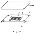
- the substrates 1a, 1b may be adhered to each other after dropping the mixed material of liquid crystals and resin in the display area as shown in Fig. 2A, a panel with a better display quality without bubbles can be obtained by dropping the mixed material of liquid crystal and resin 6 outside the display area 8 of the substrate 1b as illustrated in Figs. 2B (a) and 2C (a), putting an edge of the other substrate 1a on the substrate 1b and gradually inclining the substrate 1a along the substrate 1b as illustrated in Figs.
- FIG. 2D A diagram of the flow of the mixed material and the disappearance of the bubbles viewed from the panel plane are illustrated in Fig. 2D.
- the arrow in Fig. 2D shows the direction of the flow of the mixed material of liquid crystal and resin.
- an alignment mark 7 for aligning the substrates was formed at each edge of substrate 1b and outside a display area 8 as illustrated in Figs. 2A, 2B and 2C. Substrates 1a and 1b were fixed to each other by aligning at these marks. Since mixed material 6 was dropped in an amount more than the amount sealed between substrates 1a and 1b, it protruded beyond display area 8.
- an "opal" diffusion glass plate (DFO-15OS-1 manufactured by Sigma Koki Company Ltd.
- An "opal” diffusion glass plate comprises a transparent glass layer on which surface an opal glass layer including a photodiffusion material is affixed and it is well known in the art.) 26 was adhered to one substrate (on the side of light iraddiation) of a PDLC display panel 27 and was then placed on a reflector 28 made of aluminum or stainless steel so as to utilize reflection from the back surface. The reflector was placed on buffer 29 which was kept at 23°C by a circulating thermostat 30.
- a light transmitting film sheet 25 was sandwiched between the reflector and a quartz plate 24, and 1kg/cm 2 pressure was added to the surface of the liquid crystal display panel.
- a circulating thermostat 23 ride of a glass substrate in which water is circulating for keeping temperature constant, and quartz plate 24 for adding pressure were placed.
- a heat absorbing (or reflecting) filter for example, HAF-50S-30H manufactured by Sigma Koki Company Ltd.
- HAF-50S-30H manufactured by Sigma Koki Company Ltd.
- An ultraviolet ray cutting filter UV-35 manufactured by Toshiba Corporation 22 was also placed so as to exclude ultraviolet rays having less than 350nm wavelength and providing a negative effect on the liquid crystal transmission.
- the section except for the display area was shielded off from light, and light was irradiated onto the display area from the top substrate side with an ultra-high pressure mercury lamp (CHM-2000 manufactured by Oak Seisakusho Co., Ltd.) 20 while the panel was pressed from the bottom substrate with 1kg/cm 2 pressure.
- the phase separation of the liquid crystals and the resin in the panel was carried out by irradiating light with 50mW/cm 2 for five minutes, and the resin was cured.
- the panel was then cut along the display area circumference.
- the section except the display area was removed, and ultraviolet curing type resin (Locktite 352A manufactured by Locktite Japan Corporation) was coated along the cut surface. Ultraviolet rays were irradiated at 55mW/cm 2 for ninety seconds, thus sealing the cut surface.
- Example 1 As in Example 1, a mixed material 6 of liquid crystals 3, photosetting resin 4 and photosetting initiator was dropped on a substrate 1b in an amount greater than the volume amount sealed between the substrates. The substrate was then fixed to the other substrate. As shown in Fig. 4, the section except the peripheral section of a display area was shut off from light, and light was irradiated only to pheripheral section 8a of the display area at 50mW/cm 2 for five minutes, thus curing the resin. The shield at the display area was taken off, and light was irradiated to the area at 50mW/cm 2 for five minutes. As a result, the phase separation of the liquid crystals and the resin was carried out, and the resin was cured at the same time.
- the liquid crystal display panel was then cut along the peripheral section of the display area. After removing the unnecessary section of the panel, ultraviolet curing type resin (Locktite 352A manufactured by Locktite Japan Corporation) was coated on the cut surface of the panel. Ultraviolet rays were irradiated to the resin at 55mW/cm 2 for ninety seconds, thus sealing the cut surface. Since the mixed material of liquid crystals and resin outside the display area was applied as sealing resin in this example, it was unnecessary to form sealing resin in advance. In addition, the phase-separation in the display area was carried out after curing the peripheral section of the display area, so that a PDLC with a uniform panel gap was manufactured.
- ultraviolet curing type resin Locketite 352A manufactured by Locktite Japan Corporation
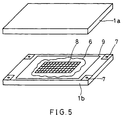
- Example 3 is explained by referring to Fig. 5.
- Transparent conductive films ITO films
- ITO films Transparent conductive films
- alignment layers AL5417 manufactured by Japan Synthetic Rubber Co., Ltd.
- the substrates were heated at 80°C for one minute and then at 220°C for thirty minutes.
- SiO 2 particles having an adherence tendency and a diameter of 13 ⁇ m (Sinsi ball AB-8-13 ⁇ m manufactured by Catalysts & Chemicals Industries Co., Ltd.) were dispersed as spacers.
- the spacers were adhered to substrate 1a after leaving the substrate at 140°C for ninety minutes, thus preventing the spacers from being displaced by dropped mixed material.
- Photo-setting resin was applied at the peripheral section of substrate 1b as seal 9.
- SiO 2 particles having diameter of 13 ⁇ m (Sinsi ball B-1 manufactured by Catalysts & Chemicals Industries Co., Ltd.) were mixed in the photosetting resin at 0.3% by weight as the spacers.
- a mixed material 6 was dropped on substrate 1b in an amount greater than the amount needed to cover the display area when the substrates are sealed.
- the mixed material includes 80% by weight of liquid crystals 3 (E-7 manufactured by British Drug House Ltd.), 1.8% by weight of polyester acrylate (photosetting resin 4), and 0.2% by weight of photosetting initiator (Darocure 1173 manufactured by Merck Co.).
- the seal was applied at the peripheral section of the substrate, and mixed material 6 of the liquid crystals and resin was dropped inside the peripheral section.
- Glass substrates 1a and 1b were adhered to each other, so that the transparent conductive films (ITO films) faced each other. As shown in Fig. 5, an alignment mark 7 for aligning the substrates was formed at each edge of the substrates outside display area 8. Substrates 1a and 1b were adhered to each other by matching the marks of substrate 1a to those of substrate 1b. Mixed material 6 was dropped between substrate 1a and 1b in an amount greater than the amount needed to cover the display area when the substrates are sealed, so that the material protruded outside the display area 8.
- ITO films transparent conductive films
- the phase separation of the liquid crystals and the resin inside the panel was carried out after irradiating light from the top substrate at 50mW/cm 2 for five minutes while pressure at 1kg/cm 2 was applied from the bottom substrate.
- the photosetting resin and seal resin 9 were cured at the same time.
- the liquid crystal panel was cut along the peripheral section of the display area, and the unnecessary section of the panel was removed.
- Ultraviolet curing type resin (Locktite 352A manufactured by Locktite Japan Corporation) was coated on the cut surface, and ultraviolet rays were irradiated to the resin at 55mW/cm 2 for ninety seconds so as to seal the cut surface.
- the mixed material of liquid crystals and photosetting resin was injected between the substrates simply, without applying a complex vacuum device. Since it was unnecessary to place the liquid crystal panel in a high vacuum atmosphere, the time required for manufacturing was significantly reduced. In addition, the seal was formed at the peripheral section of the substrate in advance, so that the substrates are matched precisely to each other.
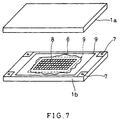
- the insulating films were formed on substrates 1a and 1b. Adhesive spacers were scattered on substrate 1a, and a mixed material was applied on substrate 1b.
- the mixed material was prepared by mixing SiO 2 particles having a diameter of 13 ⁇ m (Sinsi ball B-13 ⁇ m manufactured by Catalysts & Chemicals Industries Co., Ltd.) as spacers in photosetting resin (sealing resin). As in Fig. 6, the seal was formed intermittently outside a picture element.
- the phase separation of the liquid crystals and resin in the panel was carried out by irradiating light at 50mW/cm 2 from the top substrate for five minutes while pressure at 1kg/cm 2 was applied from the bottom substrate.
- the resin was cured at the same time.
- the panel was then cut along the peripheral section of the display area, and the unnecessary section of the panel was removed.
- Ultraviolet curing type resin (Locktite 352A manufactured by Locktite Japan Corporation) was coated on the cut surface of the substrates, and ultraviolet rays were irradiated to the resin at 55mW/cm 2 for ninety seconds so as to seal the cut surface.
- the mixed material of the liquid crystals and photocuring resin was easily injected into the substrates without applying a complex vacuum device. Unlike in the conventional method, it was unnecessary to place the liquid crystal in high vacuum atmosphere, so that the time required for manufacturing was significantly cut. By forming the seal intermittently outside a picture element, the liquid crystal panel with a uniform gap was provided.
- insulating films were formed on substrates 1a and 1b.
- adhesive spacers 5 were scattered.
- a mixed material was intermittently applied outside a picture element and was continuously applied at the peripheral section of the substrate as a seal (Fig. 7).
- the mixed material was prepared by mixing 0.3% by weight of SiO 2 particles having a diameter of 13 ⁇ m (Sinsi B-13 ⁇ m manufactured by Catalysts & Chemicals Industries Co., Ltd.) as spacers in photosetting resin (sealing resin).
- the phase-separation of the liquid crystals and resin inside the panel was carried out by irradiating light at 50mW/cm 2 for five minutes from the top substrate while pressure at 1kg/cm 2 was applied from the bottom substrate.
- the resin was cured at the same time.
- the plate was then cut along the peripheral section of the display area, and the unnecessary section of the plate was removed.
- Ultraviolet curing type resin (Locktite 352A manufactured by Locktite Japan Corporation) was coated on the cut surface of the substrates, and ultraviolet rays were irradiated to the resin at 55mW/cm 2 for ninety seconds, thus sealing the cut surface.
- the mixed material of liquid crystals and photosetting resin was injected between the substrates simply by dropping the material without applying a complex vacuum device. It was unnecessary to place the liquid crystal panel in a high vacuum atmosphere, so that the time required for manufacturing was significantly cut. Since the seal was formed intermittently outside the picture element, a liquid crystal panel with a uniform gap was provided. The seal was formed at the peripheral section of the substrates in advance, so that the substrates were precisely matched to each other.
- insulating films were applied on substrates 1a and 1b.
- adhesive spacers were applied on substrate 1a.
- a mixed material was applied outside a picture element and at the peripheral section of the substrate as a seal (Fig. 8).
- the mixed material was prepared by adding 0.3% by weight of SiO 2 particles having a diameter of 13 ⁇ m (Sinsi Ball B-13 ⁇ m manufactured by Catalysts & Chemicals Industries Co., Ltd.) as spacers in photosetting resin (seal resin). A part of the seal was applied as a guide path 9a for outflowing excess mixed material to the outside.
- the phase-separation of the liquid crystals and resin inside the panel was carried out by irradiating light at 50mW/cm 2 for five minutes from the top substrate while pressure at 1kg/cm 2 was applied from the bottom substrate.
- the resin was cured at the same time.
- the liquid crystal display panel was cut along the peripheral section of the display area, and the unnecessary section of the panel was removed.
- Ultraviolet curing type resin (Locktite 352A manufactured by Locktite Japan Corporation) was coated on the cut surface of the substrates, and ultraviolet rays were irradiated to the resin at 55mW/cm 2 for ninety seconds, thus sealing the cut surface.
- the mixed material of liquid crystals and photosetting resin was injected between the substrates simply, by dropping the material without applying a complex vacuum device. Unlike in the conventional method, it was unnecessary to place the liquid crystal panel in a high vacuum atmosphere, so that the time required for manufacturing was significantly cut. Since the guide path was formed, mixed material flowed out of the picture element. However, since the substrates were fixed by an outside seal, they were matched precisely to each other.
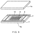
- Example 7 is explained by referring to Fig. 9.
- transparent conductive films ITO films
- ITO films transparent conductive films
- SiO 2 particles having a diameter of 13 ⁇ m were scattered on glass substrate 1a as spacers.
- an aqueous solution including 6% by weight of polyurethane as thermoplastic resin 10 (for example, MS6500 manufactured by Mitsubishi Heavy Industries, Ltd.) was printed at the edge of glass substrate 1b. Then, the substrate was heated at 80°C for one hour, thus forming a film.
- a mixed material 6 was dropped.
- the mixed material was made of 80% by weight of liquid crystals (E-7 manufactured by British Drug House Ltd.), 1.8% by weight of polyester acrylate as photosetting resin, 18% by weight of 2-ethyl hexyl acrylate, and 0.2% by weight of photosetting initiator (Darocure 1173 manufactured by Merck Co.).
- Glass substrates 1a and 1b were adhered to each other, so that the transparent conductive films (ITO films) were facing to each other.
- An alignment mark 7 was formed at each edge of the substrates outside the display area.
- the marks of substrate 1a and those of substrate 1b were matched to each other, thus aligning substrate 1a to substrate 1b. Since the mixed material of the liquid crystals and resin was dropped in an amount greater than the amount needed to cover the display area when the substrates are sealed, the material protruded outside the display area.
- Thermoplastic resin 10 was formed at the edge of glass substrate 1b. The wettability of mixed material 6 relative to thermoplastic resin 10 was poor (the contact angle was large), so that mixed material 6 did not come in contact with alignment marks 7 and precise alignment became possible.
- the section except for the display area of the panel was shielded from light, and light at 50mW/cm 2 was irradiated only to the display area for five minutes. As a result, the phase-separation of the liquid crystals and resin in the panel was carried out, and the resin was also cured. The panel was cut along the peripherial section of the display area, and the unnecessary section was removed.
- Ultraviolet curing type resin (Locktite 352A manufactured by Locktite Japan Corporation) was coated on the cut surface of the panel, and ultraviolet rays were irradiated to the cut surface at 55mW/cm 2 for ninety seconds to seal the cut surface.
- the mixed material of liquid crystals and resin was prevented from being in contact with the alignment marks since the thermoplastic resin was formed at the edge of the substrates.
- thermoplastic resin 10 was intermittently formed at the peripheral section (outside) of glass substrate 1b in this example, thermoplastic resin may be formed only at alignment marks 7.
- the thermoplastic resin is not limited to the polyurethane type, and can be a polystyrene type, polyamide type, polyvinyl chloride type, or polyethylene type. In other words, as long as the mixed material of liquid crystals and resin has a contact angle on the thermoplastic resin that is larger than a contact angle on the center of the display area, the resin can be used in the invention.
- Example 8 is explained by referrring to Fig. 10.
- transparent conductive films ITO films
- SiO 2 particles having a diameter of 13 ⁇ m were dispersed as spacers 5 on glass substrate 1a.
- an aqueous solution containing 6% by weight of polyurethane was printed as thermoplastic resin 10 (MS6500 manufactured by Mitsubishi Heavy Industries, Ltd.) at the edge of the display area on glass substrate 1b, and was treated with heat at 80 °C for one hour, thus forming a film.
- Ultravoilet curing resin was then printed as seal resin 9 at the edge of glass substrate 1b.
- a mixed material 6 was dropped on glass substrate 1b.
- the mixed material includes 80% by weight of E-7 (manufactured by British Drug House Ltd.) as liquid crystals, 1.8% by weight of polyester acrylate, and 0.2% by weight of photosetting initiator (Darocure 1173 manufactured by Merck Co.).
- thermoplastic resin 10 was formed inside seal resin 9, mixed material 6 did not come in contact with seal resin 9 after fixing the substrates to each other, thus preventing impurities in seal resin 9 from entering mixed material 6.
- the spread of the mixed material before pressing the panel was prevented by applying the thermoplastic resin at the peripheral section of the display area.
- the sealing resin was formed outside the display area in this example.
- the panel may be prepared in the following steps:
- thermoplastic resin is formed inside the display area, the mixed material is prevented from being in contact with the alignment marks.
- Example 9 is explained by referring to Fig. 11.
- transparent conductive films ITO films
- ITO films transparent conductive films
- SiO 2 particles having a diameter of 13 ⁇ m were scattered on substrate 1a as spacers.
- a mixed material 6 was dropped on glass substrate 1b.
- the mixed material included 80% by weight of liquid crystals 3 (E-7 manufactured by British Drug House Ltd.), 1.8% by weight of polyester acrylate as photosetting resin 4, 18% by weight of 2-ethyl hexyl acrylate, and 0.2% by weight of photosetting initiator (Darocure 1173 manufactured by Merck Co.).
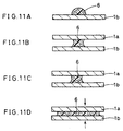
- Glass substrates 1a and 1b were set so as to face the transparent conductive films (ITO films) toward each other (Fig. 11B).
- the inside of the panel was depressurized to 1 Torr while PDLC was set in contact with one substrate (Fig. 11C).
- the substrates were fixed to each other (Fig. 11D).
- an alignment mark for fixing the substrates was formed at each edge of substrates 1a and 1b.
- the marks of substrate 1a were matched to the marks of substrate 1b.
- the section except the display area was shielded from light, and light at 50mW/cm 2 was irradiated to the display area for five minutes. As a result, the phase-separation of the liquid crystals and resin in the panel was carried out, and the resin was then cured at the same time.
- the panel was cut along the peripheral section of the display area, and the unnecessary section was removed.
- Ultraviolet curing type resin (Locktite 352A manufactured by Locktite Japan Corporation) was coated on the cut surface of the substrates, and ultraviolet rays were irradiated to the resin at 55mW/cm 2 for ninety seconds so as to seal the cut surface.
- the mixed material of polyester acrylate and 2-ethyl hexyl acrylate was applied as photosetting resin in this example.
- 2-hydroxy ethyl acrylate or trimethylol propanetriacrylate may also be used in this invention.
- thermosetting resin or thermoplastic resin may be applied and may be reacted with heat.
- E-8 manufactured by British Drug House Ltd.
- ZLI4792 manufactured by Merck Co.
- TL202 manufactured by Merck Co.
- Irgacure 184 (manufactured by Chiba-Geigy Co.) or Irgacure 651 (manufactured by Chiba-Geigy Co.) can be used as a polymerization initiator. In other words, this invention is effective without being dependent on liquid crystal materials and resin materials.
- a thermosetting agent or an agent curing at ordinary temperature may be applied as a sealing agent.
- An active matrix substrate having an active element can be applied as one of the substrates. Even though insulating films were formed on the substrate surface, the films need not be formed in this invention.
Applications Claiming Priority (3)
| Application Number | Priority Date | Filing Date | Title |
|---|---|---|---|
| JP22931694 | 1994-09-26 | ||
| JP229316/94 | 1994-09-26 | ||
| EP95115087A EP0703485B1 (de) | 1994-09-26 | 1995-09-25 | Flüssigkristallanzeigetafel, Verfahren und Vorrichtung zu ihrer Herstellung |
Related Parent Applications (1)
| Application Number | Title | Priority Date | Filing Date |
|---|---|---|---|
| EP95115087A Division EP0703485B1 (de) | 1994-09-26 | 1995-09-25 | Flüssigkristallanzeigetafel, Verfahren und Vorrichtung zu ihrer Herstellung |
Publications (2)
| Publication Number | Publication Date |
|---|---|
| EP0881525A2 true EP0881525A2 (de) | 1998-12-02 |
| EP0881525A3 EP0881525A3 (de) | 1999-03-10 |
Family
ID=16890233
Family Applications (2)
| Application Number | Title | Priority Date | Filing Date |
|---|---|---|---|
| EP95115087A Expired - Lifetime EP0703485B1 (de) | 1994-09-26 | 1995-09-25 | Flüssigkristallanzeigetafel, Verfahren und Vorrichtung zu ihrer Herstellung |
| EP98113252A Withdrawn EP0881525A3 (de) | 1994-09-26 | 1995-09-25 | Flüssigkristall-Anzeigevorrichtung und Verfahren zu ihrer Herstellung |
Family Applications Before (1)
| Application Number | Title | Priority Date | Filing Date |
|---|---|---|---|
| EP95115087A Expired - Lifetime EP0703485B1 (de) | 1994-09-26 | 1995-09-25 | Flüssigkristallanzeigetafel, Verfahren und Vorrichtung zu ihrer Herstellung |
Country Status (5)
| Country | Link |
|---|---|
| US (3) | US5854664A (de) |
| EP (2) | EP0703485B1 (de) |
| KR (1) | KR960011491A (de) |
| DE (1) | DE69526894T2 (de) |
| TW (1) | TW305949B (de) |
Cited By (2)
| Publication number | Priority date | Publication date | Assignee | Title |
|---|---|---|---|---|
| WO2005036248A1 (en) * | 2003-10-02 | 2005-04-21 | Reveo, Inc. | Liquid crystal cell assembly method and system |
| US7359028B2 (en) | 2004-03-11 | 2008-04-15 | Fujitsu Limited | Method of manufacturing liquid crystal display device |
Families Citing this family (185)
| Publication number | Priority date | Publication date | Assignee | Title |
|---|---|---|---|---|
| US5229612B1 (en) * | 1990-08-01 | 1998-04-14 | Exergen Corp | Radiation detector with remote temperature reference |
| US6011607A (en) * | 1995-02-15 | 2000-01-04 | Semiconductor Energy Laboratory Co., | Active matrix display with sealing material |
| JPH09171192A (ja) * | 1995-12-19 | 1997-06-30 | Semiconductor Energy Lab Co Ltd | アクティブマトリクス型液晶表示装置及びその製造方 法 |
| TW473629B (en) * | 1996-03-29 | 2002-01-21 | Toshiba Corp | Liquid crystal display device and its manufacture |
| US5818556A (en) * | 1996-07-24 | 1998-10-06 | Raychem Corporation | Method and apparatus for patterning encapsulated liquid crystal layers |
| WO1998005998A1 (en) * | 1996-08-07 | 1998-02-12 | Pilkington Plc | Light modulating liquid crystal devices |
| US6313894B1 (en) | 1997-03-10 | 2001-11-06 | Canon Kabushiki Kaisha | Liquid crystal display |
| TW392087B (en) * | 1997-03-10 | 2000-06-01 | Canon Kk | A liquid crystal display apparatus, a liquid crystal projector using the same, and a method of manufacturing the liquid crystal display apparatus |
| JPH1195230A (ja) * | 1997-09-19 | 1999-04-09 | Matsushita Electric Ind Co Ltd | 液晶パネルの製造方法および製造装置 |
| JP3654483B2 (ja) * | 1997-10-09 | 2005-06-02 | 富士写真フイルム株式会社 | 液晶表示装置の製造方法 |
| JP3024609B2 (ja) * | 1997-10-09 | 2000-03-21 | 日本電気株式会社 | 液晶表示素子セルの封孔装置 |
| GB9721804D0 (en) * | 1997-10-15 | 1997-12-17 | Gec Marconi Avionics Holdings | Improvements in or relating to liquid crystal displays |
| TW498179B (en) * | 1998-11-13 | 2002-08-11 | Matsushita Electric Ind Co Ltd | Light control element, optical device, and electrical device, and method of producing thereof |
| US7006193B2 (en) * | 1999-05-10 | 2006-02-28 | Au Optronics Corporation | Method of sealing two substrates with a non-epoxy or epoxy-acrylate sealant using laser radiation |
| JP2001222017A (ja) * | 1999-05-24 | 2001-08-17 | Fujitsu Ltd | 液晶表示装置及びその製造方法 |
| KR100441484B1 (ko) * | 1999-06-11 | 2004-07-23 | 세이코 엡슨 가부시키가이샤 | 액정장치 및 그 제조방법 |
| JP2001235760A (ja) * | 1999-12-14 | 2001-08-31 | Sharp Corp | 液晶表示素子の製造方法およびその製造装置 |
| US6902454B1 (en) * | 2000-07-28 | 2005-06-07 | Eastman Kodak Company | Process for laminating electrically addressable display |
| JP3903204B2 (ja) * | 2001-01-24 | 2007-04-11 | ソニー株式会社 | 表示装置の製造方法 |
| CN1193330C (zh) * | 2001-05-08 | 2005-03-16 | 松下电器产业株式会社 | 等离子体显示装置的制造方法 |
| KR100490048B1 (ko) * | 2001-06-19 | 2005-05-17 | 삼성전자주식회사 | 액정 표시 장치 제조용 인라인 시스템 및 이를 이용하는 액정 표시 장치의 제조 방법 |
| US7230670B2 (en) * | 2001-10-05 | 2007-06-12 | Lg.Philips Lcd Co., Ltd. | Method for fabricating LCD |
| CA2463679C (en) * | 2001-10-17 | 2009-08-04 | Leica Geosystems Ag | Optical telemeter |
| US6819391B2 (en) * | 2001-11-30 | 2004-11-16 | Lg. Philips Lcd Co., Ltd. | Liquid crystal display panel having dummy column spacer with opened portion |
| KR100685948B1 (ko) * | 2001-12-14 | 2007-02-23 | 엘지.필립스 엘시디 주식회사 | 액정표시소자 및 그 제조방법 |
| US7292304B2 (en) * | 2001-12-17 | 2007-11-06 | Lg.Philips Lcd Co., Ltd. | Liquid crystal display panel and method for fabricating the same comprising a dummy column spacer to regulate a liquid crystal flow and a supplemental dummy column spacer formed substantially parallel and along the dummy column spacer |
| KR100652045B1 (ko) * | 2001-12-21 | 2006-11-30 | 엘지.필립스 엘시디 주식회사 | 액정표시소자 및 그 제조방법 |
| KR100652046B1 (ko) * | 2001-12-22 | 2006-11-30 | 엘지.필립스 엘시디 주식회사 | 액정표시소자 및 그 제조방법 |
| KR100685949B1 (ko) | 2001-12-22 | 2007-02-23 | 엘지.필립스 엘시디 주식회사 | 액정표시소자 및 그 제조방법 |
| US7362407B2 (en) * | 2002-02-01 | 2008-04-22 | Lg.Philips Lcd Co., Ltd. | Method of fabricating liquid crystal display device |
| KR100510718B1 (ko) * | 2002-02-04 | 2005-08-30 | 엘지.필립스 엘시디 주식회사 | 액정표시소자의 제조 장치 |
| JP2003233080A (ja) | 2002-02-05 | 2003-08-22 | Lg Phillips Lcd Co Ltd | 合着装置及びこれを用いた液晶表示装置の製造方法 |
| KR100510719B1 (ko) * | 2002-02-05 | 2005-08-30 | 엘지.필립스 엘시디 주식회사 | 액정 표시 장치의 제조 방법 |
| KR100469353B1 (ko) * | 2002-02-06 | 2005-02-02 | 엘지.필립스 엘시디 주식회사 | 액정표시소자용 합착 장치 |
| KR100469354B1 (ko) | 2002-02-06 | 2005-02-02 | 엘지.필립스 엘시디 주식회사 | 액정 표시 장치의 제조 방법 |
| US7410109B2 (en) | 2002-02-07 | 2008-08-12 | Lg Display Co., Ltd. | Liquid crystal dispensing apparatus with nozzle protecting device |
| KR100672640B1 (ko) * | 2002-02-07 | 2007-01-23 | 엘지.필립스 엘시디 주식회사 | Uv조사장치 및 그를 이용한 액정표시소자의 제조방법 |
| KR100817129B1 (ko) * | 2002-02-07 | 2008-03-27 | 엘지.필립스 엘시디 주식회사 | 액정 패널의 절단 장치 및 그 방법 |
| KR100789454B1 (ko) | 2002-02-09 | 2007-12-31 | 엘지.필립스 엘시디 주식회사 | 액정 패널의 절단 장치 및 그 방법 |
| KR100832292B1 (ko) * | 2002-02-19 | 2008-05-26 | 엘지디스플레이 주식회사 | 액정 패널의 절단 장치 |
| US7365822B2 (en) | 2002-02-20 | 2008-04-29 | Lg.Philips Lcd Co., Ltd. | Method for fabricating LCD |
| KR100469359B1 (ko) * | 2002-02-20 | 2005-02-02 | 엘지.필립스 엘시디 주식회사 | 액정표시소자용 합착 장치 |
| KR100672641B1 (ko) * | 2002-02-20 | 2007-01-23 | 엘지.필립스 엘시디 주식회사 | 액정표시소자 및 그 제조방법 |
| KR100789455B1 (ko) | 2002-02-20 | 2007-12-31 | 엘지.필립스 엘시디 주식회사 | 액정 패널의 절단 방법 |
| KR100505180B1 (ko) * | 2002-02-20 | 2005-08-01 | 엘지.필립스 엘시디 주식회사 | 노즐세정장치를 구비한 액정적하장치 및 액정적하방법 |
| US6824023B2 (en) * | 2002-02-20 | 2004-11-30 | Lg. Philips Lcd Co., Ltd. | Liquid crystal dispensing apparatus |
| KR100532083B1 (ko) * | 2002-02-20 | 2005-11-30 | 엘지.필립스 엘시디 주식회사 | 일체화된 니들시트를 가진 액정적하장치 |
| US7006202B2 (en) * | 2002-02-21 | 2006-02-28 | Lg.Philips Lcd Co., Ltd. | Mask holder for irradiating UV-rays |
| US6864948B2 (en) | 2002-02-22 | 2005-03-08 | Lg.Philips Lcd Co., Ltd. | Apparatus for measuring dispensing amount of liquid crystal drops and method for manufacturing liquid crystal display device using the same |
| KR100469360B1 (ko) * | 2002-02-22 | 2005-02-02 | 엘지.필립스 엘시디 주식회사 | 액정표시소자의 제조 장비용 진공 합착 장치 및 구동 방법 |
| KR100741897B1 (ko) * | 2002-03-22 | 2007-07-24 | 엘지.필립스 엘시디 주식회사 | 가스 온도 조절 기능을 갖는 합착 장치 |
| KR100469508B1 (ko) | 2002-02-22 | 2005-02-02 | 엘지.필립스 엘시디 주식회사 | 스프링의 장력조정에 의해 액정적하량을 제어가 가능한액정적하장치 |
| US6712883B2 (en) | 2002-02-25 | 2004-03-30 | Lg.Philips Lcd Co., Ltd. | Apparatus and method for deaerating liquid crystal |
| US6803984B2 (en) | 2002-02-25 | 2004-10-12 | Lg.Philips Lcd Co., Ltd. | Method and apparatus for manufacturing liquid crystal display device using serial production processes |
| US8074551B2 (en) * | 2002-02-26 | 2011-12-13 | Lg Display Co., Ltd. | Cutting wheel for liquid crystal display panel |
| US6774958B2 (en) * | 2002-02-26 | 2004-08-10 | Lg.Philips Lcd Co., Ltd. | Liquid crystal panel, apparatus for inspecting the same, and method of fabricating liquid crystal display thereof |
| US6833901B2 (en) * | 2002-02-27 | 2004-12-21 | Lg. Philips Lcd Co., Ltd. | Method for fabricating LCD having upper substrate coated with sealant |
| US6784970B2 (en) * | 2002-02-27 | 2004-08-31 | Lg.Philips Lcd Co., Ltd. | Method of fabricating LCD |
| KR100720414B1 (ko) * | 2002-02-27 | 2007-05-22 | 엘지.필립스 엘시디 주식회사 | 액정 표시 장치의 제조 방법 |
| KR100511352B1 (ko) * | 2002-02-27 | 2005-08-31 | 엘지.필립스 엘시디 주식회사 | 액정적하장치 및 액정적하량 제어방법 |
| US7270587B2 (en) * | 2002-03-05 | 2007-09-18 | Lg.Philips Lcd Co., Ltd. | Apparatus and method for manufacturing liquid crystal display devices, method for using the apparatus, and device produced by the method |
| KR100685951B1 (ko) * | 2002-03-06 | 2007-02-23 | 엘지.필립스 엘시디 주식회사 | 액정표시소자 및 그 제조방법 |
| KR100798320B1 (ko) | 2002-03-06 | 2008-01-28 | 엘지.필립스 엘시디 주식회사 | 액정 패널의 검사 장치 및 그 방법 |
| KR100606966B1 (ko) * | 2002-03-06 | 2006-08-01 | 엘지.필립스 엘시디 주식회사 | 액정표시소자의 제조라인 |
| KR100662495B1 (ko) * | 2002-03-07 | 2007-01-02 | 엘지.필립스 엘시디 주식회사 | 액정표시소자의 제조방법 |
| JP2003270652A (ja) * | 2002-03-08 | 2003-09-25 | Lg Phillips Lcd Co Ltd | 液晶拡散制御装置及び液晶表示装置の製造方法 |
| KR100720415B1 (ko) | 2002-03-08 | 2007-05-22 | 엘지.필립스 엘시디 주식회사 | 액정표시소자 제조 공정용 반송 장치 |
| US7416010B2 (en) * | 2002-03-08 | 2008-08-26 | Lg Display Co., Ltd. | Bonding apparatus and system for fabricating liquid crystal display device |
| KR100807587B1 (ko) * | 2002-03-09 | 2008-02-28 | 엘지.필립스 엘시디 주식회사 | 액정 패널의 절단 방법 |
| US7027122B2 (en) * | 2002-03-12 | 2006-04-11 | Lg.Philips Lcd Co., Ltd. | Bonding apparatus having compensating system for liquid crystal display device and method for manufacturing the same |
| US6892437B2 (en) | 2002-03-13 | 2005-05-17 | Lg. Philips Lcd Co., Ltd. | Apparatus and method for manufacturing liquid crystal display device |
| KR100817130B1 (ko) * | 2002-03-13 | 2008-03-27 | 엘지.필립스 엘시디 주식회사 | 액정 패널의 연마량 검출 패턴 및 이를 이용한 연마불량판단 방법 |
| KR100870661B1 (ko) | 2002-03-15 | 2008-11-26 | 엘지디스플레이 주식회사 | 기판 수납용 카세트 |
| US7698833B2 (en) * | 2002-03-15 | 2010-04-20 | Lg Display Co., Ltd. | Apparatus for hardening a sealant located between a pair bonded substrates of liquid crystal display device |
| US6782928B2 (en) * | 2002-03-15 | 2004-08-31 | Lg.Philips Lcd Co., Ltd. | Liquid crystal dispensing apparatus having confirming function for remaining amount of liquid crystal and method for measuring the same |
| US6885427B2 (en) * | 2002-03-15 | 2005-04-26 | Lg.Philips Lcd Co., Ltd. | Substrate bonding apparatus for liquid crystal display device having alignment system with one end provided inside vacuum chamber |
| US7102726B2 (en) * | 2002-03-15 | 2006-09-05 | Lg. Philips Lcd Co., Ltd. | System for fabricating liquid crystal display and method of fabricating liquid crystal display using the same |
| KR100817131B1 (ko) * | 2002-03-15 | 2008-03-27 | 엘지.필립스 엘시디 주식회사 | 액정 패널의 검사 장치 및 그 방법 |
| KR100817132B1 (ko) * | 2002-03-15 | 2008-03-27 | 엘지.필립스 엘시디 주식회사 | 액정적하장치 |
| KR100720416B1 (ko) * | 2002-03-16 | 2007-05-22 | 엘지.필립스 엘시디 주식회사 | 액정표시소자용 합착 장치 |
| KR100685952B1 (ko) * | 2002-03-19 | 2007-02-23 | 엘지.필립스 엘시디 주식회사 | 액정표시소자용 기판, 액정표시소자 및 그 제조방법 |
| US7040525B2 (en) * | 2002-03-20 | 2006-05-09 | Lg.Philips Lcd Co., Ltd. | Stage structure in bonding machine and method for controlling the same |
| US7341641B2 (en) * | 2002-03-20 | 2008-03-11 | Lg.Philips Lcd Co., Ltd. | Bonding device for manufacturing liquid crystal display device |
| KR100854378B1 (ko) * | 2002-03-20 | 2008-08-26 | 엘지디스플레이 주식회사 | 액정 패널 및 그 제조방법 |
| KR100480819B1 (ko) | 2002-03-20 | 2005-04-06 | 엘지.필립스 엘시디 주식회사 | 합착기 챔버의 크리닝 방법 |
| KR100832293B1 (ko) | 2002-03-20 | 2008-05-26 | 엘지디스플레이 주식회사 | 액정 패널의 연마대 및 이를 이용한 연마장치 |
| KR100652050B1 (ko) * | 2002-03-20 | 2006-11-30 | 엘지.필립스 엘시디 주식회사 | 액정표시소자 및 그 제조방법 |
| KR100798322B1 (ko) * | 2002-03-21 | 2008-01-28 | 엘지.필립스 엘시디 주식회사 | 액정 패널의 연마량 보정 장치 및 방법 |
| KR100841623B1 (ko) | 2002-03-21 | 2008-06-27 | 엘지디스플레이 주식회사 | 액정 패널의 연마장치 |
| US6874662B2 (en) | 2002-03-21 | 2005-04-05 | Lg. Philips Lcd Co., Ltd. | Liquid crystal dispensing apparatus |
| US6827240B2 (en) | 2002-03-21 | 2004-12-07 | Lg.Philips Lcd Co., Ltd. | Liquid crystal dispensing apparatus |
| US6793756B2 (en) * | 2002-03-22 | 2004-09-21 | Lg. Phillips Lcd Co., Ltd. | Substrate bonding apparatus for liquid crystal display device and method for driving the same |
| JP4210139B2 (ja) * | 2002-03-23 | 2009-01-14 | エルジー ディスプレイ カンパニー リミテッド | スペーサの高さによって液晶の滴下量調整が可能である液晶滴下装置及びその滴下方法 |
| US7244160B2 (en) * | 2002-03-23 | 2007-07-17 | Lg.Philips Lcd Co., Ltd. | Liquid crystal display device bonding apparatus and method of using the same |
| KR100885840B1 (ko) * | 2002-03-23 | 2009-02-27 | 엘지디스플레이 주식회사 | 셀갭의 보정이 가능한 액정패널구조 |
| KR100662496B1 (ko) * | 2002-03-23 | 2007-01-02 | 엘지.필립스 엘시디 주식회사 | 액정표시소자 및 그 제조방법 |
| KR100860522B1 (ko) * | 2002-03-23 | 2008-09-26 | 엘지디스플레이 주식회사 | 액정 패널의 이송장치 |
| KR20030077070A (ko) * | 2002-03-25 | 2003-10-01 | 엘지.필립스 엘시디 주식회사 | 중력불량측정용 카세트 |
| KR100685923B1 (ko) * | 2002-03-25 | 2007-02-23 | 엘지.필립스 엘시디 주식회사 | 합착 장치 및 이를 이용한 액정표시장치의 제조 방법 |
| KR100518269B1 (ko) * | 2002-03-25 | 2005-10-04 | 엘지.필립스 엘시디 주식회사 | 복수의 액정적하기를 이용한 액정적하방법 |
| KR100848556B1 (ko) * | 2002-03-25 | 2008-07-25 | 엘지디스플레이 주식회사 | 액정 패널의 회전 버퍼 및 이를 이용한 러빙장치 |
| KR100720420B1 (ko) * | 2002-03-25 | 2007-05-22 | 엘지.필립스 엘시디 주식회사 | 액정표시소자용 합착 장치의 동작 제어 방법 및 그 장치 |
| KR100817134B1 (ko) * | 2002-03-25 | 2008-03-27 | 엘지.필립스 엘시디 주식회사 | 액정 패널의 제조장치 및 방법 |
| KR100640994B1 (ko) * | 2002-03-25 | 2006-11-02 | 엘지.필립스 엘시디 주식회사 | 씨일재 탈포용기 및 그를 이용한 씨일재 탈포장비 |
| TW595263B (en) * | 2002-04-12 | 2004-06-21 | O2Micro Inc | A circuit structure for driving cold cathode fluorescent lamp |
| US7649674B2 (en) | 2002-06-10 | 2010-01-19 | E Ink Corporation | Electro-optic display with edge seal |
| KR100698039B1 (ko) | 2002-06-14 | 2007-03-23 | 엘지.필립스 엘시디 주식회사 | 세정용 지그 |
| KR100698040B1 (ko) | 2002-06-14 | 2007-03-23 | 엘지.필립스 엘시디 주식회사 | 이동용 지그 |
| US7225917B2 (en) * | 2002-06-15 | 2007-06-05 | Lg.Philips Lcd Co., Ltd. | Conveyor system having width adjustment unit |
| KR20030095888A (ko) * | 2002-06-15 | 2003-12-24 | 엘지.필립스 엘시디 주식회사 | 액정 패널의 이송장치 |
| US7295279B2 (en) * | 2002-06-28 | 2007-11-13 | Lg.Philips Lcd Co., Ltd. | System and method for manufacturing liquid crystal display devices |
| KR100488535B1 (ko) | 2002-07-20 | 2005-05-11 | 엘지.필립스 엘시디 주식회사 | 액정토출장치 및 토출방법 |
| US7063758B2 (en) * | 2002-07-29 | 2006-06-20 | Three Bond Co., Ltd. | Laminating apparatus and laminating method |
| KR100675628B1 (ko) * | 2002-10-16 | 2007-02-01 | 엘지.필립스 엘시디 주식회사 | 절연막 식각장치 및 식각방법 |
| KR100724474B1 (ko) * | 2002-10-22 | 2007-06-04 | 엘지.필립스 엘시디 주식회사 | 액정 표시패널의 절단 장치 및 이를 이용한 절단방법 |
| KR100493384B1 (ko) * | 2002-11-07 | 2005-06-07 | 엘지.필립스 엘시디 주식회사 | 액정표시소자 제조 공정용 기판 합착 장치의 기판을로딩하기 위한 구조 |
| KR100689310B1 (ko) * | 2002-11-11 | 2007-03-08 | 엘지.필립스 엘시디 주식회사 | 액정 표시패널의 디스펜서 및 이를 이용한 노즐과 기판의갭 제어방법 |
| KR100618577B1 (ko) | 2002-11-13 | 2006-08-31 | 엘지.필립스 엘시디 주식회사 | 액정 표시패널의 디스펜서 및 이를 이용한 디스펜싱 방법 |
| KR100724475B1 (ko) * | 2002-11-13 | 2007-06-04 | 엘지.필립스 엘시디 주식회사 | 액정 표시패널의 실 디스펜서 및 이를 이용한 실 패턴의단선 검출방법 |
| KR100724476B1 (ko) * | 2002-11-13 | 2007-06-04 | 엘지.필립스 엘시디 주식회사 | 액정 표시패널의 디스펜서 및 이를 이용한 디스펜싱물질의 잔여량 검출방법 |
| KR100618576B1 (ko) | 2002-11-13 | 2006-08-31 | 엘지.필립스 엘시디 주식회사 | 액정 표시패널의 디스펜서 및 이를 이용한 디스펜싱 방법 |
| KR100720422B1 (ko) * | 2002-11-15 | 2007-05-22 | 엘지.필립스 엘시디 주식회사 | 액정표시소자 제조 장치 및 이를 이용한 제조 방법 |
| TWI257515B (en) * | 2002-11-16 | 2006-07-01 | Lg Philips Lcd Co Ltd | Substrate bonding apparatus for liquid crystal display device |
| US7275577B2 (en) * | 2002-11-16 | 2007-10-02 | Lg.Philips Lcd Co., Ltd. | Substrate bonding machine for liquid crystal display device |
| KR100720449B1 (ko) * | 2002-11-18 | 2007-05-22 | 엘지.필립스 엘시디 주식회사 | 액정표시소자 제조 장치 |
| KR100662497B1 (ko) | 2002-11-18 | 2007-01-02 | 엘지.필립스 엘시디 주식회사 | 액정표시소자 제조 공정용 기판 합착 장치 |
| KR100724477B1 (ko) * | 2002-11-19 | 2007-06-04 | 엘지.필립스 엘시디 주식회사 | 액정 표시패널의 디스펜서 및 이를 이용한 디스펜싱 방법 |
| KR100710163B1 (ko) * | 2002-11-28 | 2007-04-20 | 엘지.필립스 엘시디 주식회사 | 액정표시장치의 제조방법 |
| KR100710162B1 (ko) * | 2002-11-28 | 2007-04-20 | 엘지.필립스 엘시디 주식회사 | 액정표시장치의 실 패턴 형성방법 |
| KR100832297B1 (ko) * | 2002-12-17 | 2008-05-26 | 엘지디스플레이 주식회사 | 액정 표시패널의 연마량 측정장치 및 측정방법 |
| KR100700176B1 (ko) * | 2002-12-18 | 2007-03-27 | 엘지.필립스 엘시디 주식회사 | 액정 표시패널의 디스펜서 및 이를 이용한 노즐과 기판의갭 제어방법 |
| KR100771907B1 (ko) * | 2002-12-20 | 2007-11-01 | 엘지.필립스 엘시디 주식회사 | 액정 표시패널의 디스펜서 및 디스펜싱방법 |
| KR100618578B1 (ko) * | 2002-12-20 | 2006-08-31 | 엘지.필립스 엘시디 주식회사 | 액정 표시패널의 디스펜서 및 이를 이용한 디스펜싱 방법 |
| KR100618579B1 (ko) * | 2002-12-23 | 2006-08-31 | 엘지.필립스 엘시디 주식회사 | 디스펜서 정렬장치 및 그 방법 |
| KR100652212B1 (ko) * | 2002-12-30 | 2006-11-30 | 엘지.필립스 엘시디 주식회사 | 액정패널의 제조방법 및 이에 사용되는 씰패턴 형성장치 |
| KR100996576B1 (ko) | 2003-05-09 | 2010-11-24 | 주식회사 탑 엔지니어링 | 액정적하장치 및 액정적하방법 |
| KR100923680B1 (ko) * | 2003-04-29 | 2009-10-28 | 엘지디스플레이 주식회사 | 액정 표시패널의 절단장치 |
| US6937315B2 (en) * | 2003-05-01 | 2005-08-30 | Chunghwa Picture Tubes, Ltd. | Liquid crystal panel with isolation wall structure and its producing method |
| KR20040104037A (ko) * | 2003-06-02 | 2004-12-10 | 엘지.필립스 엘시디 주식회사 | 액정 표시패널의 디스펜서 |
| KR100939629B1 (ko) * | 2003-06-02 | 2010-01-29 | 엘지디스플레이 주식회사 | 액정 표시패널의 실린지 |
| KR100566455B1 (ko) * | 2003-06-24 | 2006-03-31 | 엘지.필립스 엘시디 주식회사 | 스페이서정보를 이용한 액정적하장치 및 액정적하방법 |
| KR100996554B1 (ko) * | 2003-06-24 | 2010-11-24 | 엘지디스플레이 주식회사 | 분리가능한 액정토출펌프를 구비한 액정적하장치 |
| KR100557500B1 (ko) * | 2003-06-24 | 2006-03-07 | 엘지.필립스 엘시디 주식회사 | 액정용기의 정보가 판독 가능한 액정적하장치 및 이를이용한 액정적하방법 |
| KR100966451B1 (ko) | 2003-06-25 | 2010-06-28 | 엘지디스플레이 주식회사 | 액정적하장치 |
| KR100495476B1 (ko) * | 2003-06-27 | 2005-06-14 | 엘지.필립스 엘시디 주식회사 | 액정적하장치 |
| US6892769B2 (en) | 2003-06-30 | 2005-05-17 | Lg.Philips Lcd Co., Ltd. | Substrate bonding apparatus for liquid crystal display device panel |
| US7285900B2 (en) * | 2003-10-22 | 2007-10-23 | Teco Nanotech Co., Ltd. | Field emission display having self-adhesive frame |
| KR20050041697A (ko) | 2003-10-31 | 2005-05-04 | 엘지.필립스 엘시디 주식회사 | 액정 표시패널의 러빙장치 |
| CN100362399C (zh) | 2003-11-17 | 2008-01-16 | Lg.菲利浦Lcd株式会社 | 液晶分配方法和装置 |
| KR100689313B1 (ko) * | 2003-11-22 | 2007-03-08 | 엘지.필립스 엘시디 주식회사 | 은-실런트 복합화 디스펜서 및 이를 이용한액정표시패널의 디스펜싱 방법 |
| KR100987897B1 (ko) * | 2003-11-25 | 2010-10-13 | 엘지디스플레이 주식회사 | 액정 표시패널의 디스펜서 및 이를 이용한 디스펜싱 방법 |
| KR100987910B1 (ko) * | 2003-11-28 | 2010-10-13 | 엘지디스플레이 주식회사 | 액정적하장치 및 액정적하방법 |
| KR100689314B1 (ko) * | 2003-11-29 | 2007-03-08 | 엘지.필립스 엘시디 주식회사 | 액정표시패널의 절단방법 |
| US8146641B2 (en) * | 2003-12-01 | 2012-04-03 | Lg Display Co., Ltd. | Sealant hardening apparatus of liquid crystal display panel and sealant hardening method thereof |
| US7349060B2 (en) | 2003-12-02 | 2008-03-25 | Lg.Philips Lcd Co., Ltd. | Loader and bonding apparatus for fabricating liquid crystal display device and loading method thereof |
| KR20050056799A (ko) * | 2003-12-10 | 2005-06-16 | 엘지.필립스 엘시디 주식회사 | 액정 표시패널의 실 패턴 구조 |
| KR101026935B1 (ko) | 2003-12-10 | 2011-04-04 | 엘지디스플레이 주식회사 | 디스펜서 정렬장치 및 그 방법 |
| US8203685B2 (en) * | 2003-12-10 | 2012-06-19 | Lg Display Co., Ltd. | Liquid crystal display panel having seal pattern for minimizing liquid crystal contamination and method of manufacturing the same |
| KR101003666B1 (ko) * | 2003-12-10 | 2010-12-23 | 엘지디스플레이 주식회사 | 정렬장치 |
| KR101025067B1 (ko) * | 2003-12-13 | 2011-03-25 | 엘지디스플레이 주식회사 | 액정 표시패널의 제조장치 |
| KR101010450B1 (ko) | 2003-12-17 | 2011-01-21 | 엘지디스플레이 주식회사 | 액정적하장치 |
| CN100359393C (zh) | 2003-12-17 | 2008-01-02 | Lg.菲利浦Lcd株式会社 | 液晶分配装置 |
| KR100710169B1 (ko) * | 2003-12-26 | 2007-04-20 | 엘지.필립스 엘시디 주식회사 | 액정 표시 장치의 제조 라인 및 제조 방법 |
| KR100972502B1 (ko) * | 2003-12-30 | 2010-07-26 | 엘지디스플레이 주식회사 | 액정표시장치의 등급표시 자동화 장치 및 이의 동작 방법 |
| KR101003603B1 (ko) * | 2003-12-30 | 2010-12-23 | 엘지디스플레이 주식회사 | 액정 표시패널의 디스펜서 및 이를 이용한 디스펜싱 방법 |
| US7075703B2 (en) * | 2004-01-16 | 2006-07-11 | E Ink Corporation | Process for sealing electro-optic displays |
| JP2005300972A (ja) * | 2004-04-13 | 2005-10-27 | Seiko Epson Corp | 表示装置の製造方法及び基板貼り合わせ装置 |
| KR100640216B1 (ko) * | 2004-05-29 | 2006-10-31 | 엘지.필립스 엘시디 주식회사 | 액정 표시패널 및 그 제조방법 |
| JP4381938B2 (ja) * | 2004-09-09 | 2009-12-09 | シャープ株式会社 | 液晶表示パネル及びその検査方法並びにそれに用いる検査装置 |
| KR20060079721A (ko) * | 2005-01-03 | 2006-07-06 | 삼성전자주식회사 | 액정 표시 장치용 표시판의 제조 방법 |
| WO2007102197A1 (ja) * | 2006-03-07 | 2007-09-13 | Fujitsu Limited | 液晶表示パネルの製造方法及び装置 |
| US8610988B2 (en) | 2006-03-09 | 2013-12-17 | E Ink Corporation | Electro-optic display with edge seal |
| US7666713B2 (en) * | 2006-03-24 | 2010-02-23 | Fujitsu Limited | Method for bonding heatsink and semiconductor device with heatsink |
| US8502952B2 (en) | 2007-04-14 | 2013-08-06 | Industrial Technology Research Institute | Color cholesteric liquid crystal display devices and fabrication methods thereof |
| US8562770B2 (en) | 2008-05-21 | 2013-10-22 | Manufacturing Resources International, Inc. | Frame seal methods for LCD |
| US9573346B2 (en) * | 2008-05-21 | 2017-02-21 | Manufacturing Resources International, Inc. | Photoinitiated optical adhesive and method for using same |
| WO2011018916A1 (ja) | 2009-08-12 | 2011-02-17 | コニカミノルタホールディングス株式会社 | 表示パネルの製造方法 |
| JP2011141409A (ja) * | 2010-01-07 | 2011-07-21 | Canon Inc | ディスプレイの製造方法 |
| US9884475B2 (en) | 2011-01-19 | 2018-02-06 | Precision Valve & Automation, Inc. | Machine for optical bonding, system and method of use thereof |
| US20120180935A1 (en) | 2011-01-19 | 2012-07-19 | Vannorden Jeffrey James | Robotic placement machine for optical bonding, system and method of use thereof |
| JP5411905B2 (ja) | 2011-09-30 | 2014-02-12 | オリジン電気株式会社 | 接合部材の製造装置及び接合部材の製造方法 |
| US20140071392A1 (en) * | 2012-09-07 | 2014-03-13 | Apple Inc. | Initial contact control for lamination |
| KR102038740B1 (ko) * | 2016-07-19 | 2019-10-31 | (주)화이트스톤 | 곡면 커버 글라스 보호필름, 이의 부착장치 및 이를 이용한 곡면 커버 글라스 보호필름의 부착방법 |
| US11133580B2 (en) * | 2017-06-22 | 2021-09-28 | Innolux Corporation | Antenna device |
| US10782569B2 (en) * | 2018-09-30 | 2020-09-22 | HKC Corporation Limited | Display panel and a display device |
Citations (6)
| Publication number | Priority date | Publication date | Assignee | Title |
|---|---|---|---|---|
| JPH0437820A (ja) * | 1990-06-04 | 1992-02-07 | Seiko Epson Corp | 液晶表示素子の製造方法 |
| JPH0460518A (ja) * | 1990-06-29 | 1992-02-26 | Kyoritsu Kagaku Sangyo Kk | 液晶表示装置の製造方法 |
| US5106441A (en) * | 1989-01-26 | 1992-04-21 | Nokia Unterhaltungselektronik | Method and jig for lcd-production |
| JPH055890A (ja) * | 1991-06-27 | 1993-01-14 | Sanyo Electric Co Ltd | 液晶表示パネルおよびその製造方法 |
| JPH05297381A (ja) * | 1991-06-28 | 1993-11-12 | Nippon Seiki Co Ltd | 液晶表示装置 |
| JPH06102498A (ja) * | 1992-08-04 | 1994-04-15 | Matsushita Electric Ind Co Ltd | 液晶パネルの製造方法 |
Family Cites Families (19)
| Publication number | Priority date | Publication date | Assignee | Title |
|---|---|---|---|---|
| US3990782A (en) * | 1974-09-09 | 1976-11-09 | Beckman Instruments, Inc. | Seal for liquid crystal display cell |
| US4094058A (en) * | 1976-07-23 | 1978-06-13 | Omron Tateisi Electronics Co. | Method of manufacture of liquid crystal displays |
| US4640583A (en) * | 1983-07-22 | 1987-02-03 | Kabushiki Kaisha Seiko Epson | Display panel having an inner and an outer seal and process for the production thereof |
| JPS61190313A (ja) | 1985-02-20 | 1986-08-25 | Matsushita Electric Ind Co Ltd | 液晶パネルの製造方法 |
| US5176140A (en) * | 1989-08-14 | 1993-01-05 | Olympus Optical Co., Ltd. | Ultrasonic probe |
| JPH04218027A (ja) * | 1990-06-14 | 1992-08-07 | Hoechst Japan Ltd | 液晶セルの製造法 |
| US5030018A (en) * | 1990-09-06 | 1991-07-09 | Itt Corporation | Adjustment device for centrifugal pump impeller |
| US5474629A (en) * | 1990-12-15 | 1995-12-12 | Semiconductor Energy Laboratory Co., Ltd. | Method for manufacturing a liquid crystal device |
| JP2992648B2 (ja) * | 1990-12-20 | 1999-12-20 | 株式会社半導体エネルギー研究所 | 液晶電気光学装置の作製方法 |
| JPH055892A (ja) * | 1991-06-27 | 1993-01-14 | Sanyo Electric Co Ltd | 液晶表示パネルおよびその製造方法 |
| JPH055893A (ja) * | 1991-06-27 | 1993-01-14 | Sanyo Electric Co Ltd | 液晶表示パネルおよびその製造方法 |
| JP3207282B2 (ja) * | 1992-05-15 | 2001-09-10 | 富士通株式会社 | ポリマー分散型液晶表示装置の製造方法 |
| US5499127A (en) * | 1992-05-25 | 1996-03-12 | Sharp Kabushiki Kaisha | Liquid crystal display device having a larger gap between the substrates in the display area than in the sealant area |
| JPH06235925A (ja) * | 1993-02-10 | 1994-08-23 | Matsushita Electric Ind Co Ltd | 液晶表示素子の製造方法 |
| FR2702058B1 (fr) * | 1993-02-23 | 1995-04-07 | Thomson Csf | Procédé d'obtention de matériaux composites à base de polymère et de cristaux liquides avec colorants dichroiques. |
| JPH0676929U (ja) * | 1993-03-31 | 1994-10-28 | カシオ計算機株式会社 | 高分子分散型液晶表示素子の製造装置 |
| US5552913A (en) * | 1993-06-03 | 1996-09-03 | Semiconductor Energy Laboratory Co., Ltd. | Liquid crystal device and method for producing the same |
| KR0163981B1 (ko) * | 1993-06-29 | 1999-01-15 | 사또오 아키오 | 필름제 액정셀 봉지용 수지조성물 |
| US5617228A (en) * | 1994-07-13 | 1997-04-01 | Kabushiki Kaisha Toshiba | Polymer-dispersed liquid crystal display device and method to set liquid crystal layer thickness in association with driving voltage |
-
1995
- 1995-09-25 DE DE69526894T patent/DE69526894T2/de not_active Expired - Fee Related
- 1995-09-25 EP EP95115087A patent/EP0703485B1/de not_active Expired - Lifetime
- 1995-09-25 EP EP98113252A patent/EP0881525A3/de not_active Withdrawn
- 1995-09-25 US US08/533,149 patent/US5854664A/en not_active Expired - Fee Related
- 1995-09-26 KR KR1019950031756A patent/KR960011491A/ko not_active Application Discontinuation
- 1995-09-29 TW TW084110184A patent/TW305949B/zh active
-
1997
- 1997-05-27 US US08/863,218 patent/US5852484A/en not_active Expired - Fee Related
- 1997-05-27 US US08/863,217 patent/US5872608A/en not_active Expired - Fee Related
Patent Citations (6)
| Publication number | Priority date | Publication date | Assignee | Title |
|---|---|---|---|---|
| US5106441A (en) * | 1989-01-26 | 1992-04-21 | Nokia Unterhaltungselektronik | Method and jig for lcd-production |
| JPH0437820A (ja) * | 1990-06-04 | 1992-02-07 | Seiko Epson Corp | 液晶表示素子の製造方法 |
| JPH0460518A (ja) * | 1990-06-29 | 1992-02-26 | Kyoritsu Kagaku Sangyo Kk | 液晶表示装置の製造方法 |
| JPH055890A (ja) * | 1991-06-27 | 1993-01-14 | Sanyo Electric Co Ltd | 液晶表示パネルおよびその製造方法 |
| JPH05297381A (ja) * | 1991-06-28 | 1993-11-12 | Nippon Seiki Co Ltd | 液晶表示装置 |
| JPH06102498A (ja) * | 1992-08-04 | 1994-04-15 | Matsushita Electric Ind Co Ltd | 液晶パネルの製造方法 |
Non-Patent Citations (4)
| Title |
|---|
| PATENT ABSTRACTS OF JAPAN vol. 16, no. 211 (P-1355) & JP 04 037820 A (SEIKO) * |
| PATENT ABSTRACTS OF JAPAN vol. 16, no. 252 (P-1367) & JP 04 060518 A (KIYOURITSU KAGAKU) * |
| PATENT ABSTRACTS OF JAPAN vol. 17, no. 265 (P-1542) & JP 05 005890 A (SANYO) * |
| PATENT ABSTRACTS OF JAPAN vol. 18, no. 373 (P-1769) & JP 06 102498 A (MATSUSHITA) & US 5 426 522 A (MATSUSHITA) 20 June 1995 * |
Cited By (2)
| Publication number | Priority date | Publication date | Assignee | Title |
|---|---|---|---|---|
| WO2005036248A1 (en) * | 2003-10-02 | 2005-04-21 | Reveo, Inc. | Liquid crystal cell assembly method and system |
| US7359028B2 (en) | 2004-03-11 | 2008-04-15 | Fujitsu Limited | Method of manufacturing liquid crystal display device |
Also Published As
| Publication number | Publication date |
|---|---|
| KR960011491A (ko) | 1996-04-20 |
| EP0703485B1 (de) | 2002-06-05 |
| DE69526894D1 (de) | 2002-07-11 |
| EP0881525A3 (de) | 1999-03-10 |
| US5872608A (en) | 1999-02-16 |
| DE69526894T2 (de) | 2003-01-23 |
| US5854664A (en) | 1998-12-29 |
| EP0703485A2 (de) | 1996-03-27 |
| US5852484A (en) | 1998-12-22 |
| EP0703485A3 (de) | 1997-07-30 |
| TW305949B (de) | 1997-05-21 |
Similar Documents
| Publication | Publication Date | Title |
|---|---|---|
| EP0703485B1 (de) | Flüssigkristallanzeigetafel, Verfahren und Vorrichtung zu ihrer Herstellung | |
| US5365356A (en) | Method of fabricating an encapsulated liquid crystal display | |
| US5729312A (en) | LCD and method for producing the same in which a larger number of substrate gap control materials is larger in the polymer walls than in the liquid crystal regions | |
| KR100685948B1 (ko) | 액정표시소자 및 그 제조방법 | |
| JP2001356354A (ja) | 液晶表示素子の製造方法 | |
| JPH0713138A (ja) | 高分子分散型液晶表示素子 | |
| JPH0973096A (ja) | 液晶表示素子の製造方法 | |
| US6341000B1 (en) | Liquid-crystal panel of polymer dispersed type and method of manufacturing the same | |
| JPS6145224A (ja) | 液晶表示素子の製造方法 | |
| US6246456B1 (en) | Liquid-crystal panel of polymer dispersed type, method of manufacturing the same, and liquid-crystal display apparatus | |
| WO2020186567A1 (zh) | 液晶显示面板的制作方法及液晶显示面板 | |
| JP3077740B2 (ja) | 液晶パネルとその製造方法及びその製造装置 | |
| JP3092899B2 (ja) | 液晶表示素子およびその製造方法 | |
| JP2800422B2 (ja) | 液晶表示素子とその製造方法 | |
| JP4362220B2 (ja) | Uvキュアラブル液晶を用いた液晶セルの製造方法 | |
| JPH07120758A (ja) | 高分子分散型液晶表示装置 | |
| JP2001215484A (ja) | 印刷用液晶インクおよびこれを用いた液晶表示素子 | |
| JPH0815710A (ja) | 液晶パネル,その製造方法及び液晶表示装置 | |
| JP2001075111A (ja) | 液晶素子製造方法 | |
| JPH05249440A (ja) | 液晶表示素子 | |
| JPH09230322A (ja) | 液晶光学素子およびその製造方法 | |
| JPH04107530A (ja) | 液晶パネルの製造方法 | |
| JPH04208924A (ja) | 液晶パネルの製造方法 | |
| JPH09318944A (ja) | 液晶表示素子の製造方法及びバックライトの製造方法並びにその製造システム | |
| JPS6132035A (ja) | 液晶表示素子の製造方法 |
Legal Events
| Date | Code | Title | Description |
|---|---|---|---|
| PUAI | Public reference made under article 153(3) epc to a published international application that has entered the european phase |
Free format text: ORIGINAL CODE: 0009012 |
|
| AC | Divisional application: reference to earlier application |
Ref document number: 703485 Country of ref document: EP |
|
| AK | Designated contracting states |
Kind code of ref document: A2 Designated state(s): DE FR NL |
|
| PUAL | Search report despatched |
Free format text: ORIGINAL CODE: 0009013 |
|
| AK | Designated contracting states |
Kind code of ref document: A3 Designated state(s): DE FR NL |
|
| RHK1 | Main classification (correction) |
Ipc: G02F 1/1333 |
|
| 17P | Request for examination filed |
Effective date: 19990416 |
|
| 17Q | First examination report despatched |
Effective date: 20001114 |
|
| GRAP | Despatch of communication of intention to grant a patent |
Free format text: ORIGINAL CODE: EPIDOSNIGR1 |
|
| GRAP | Despatch of communication of intention to grant a patent |
Free format text: ORIGINAL CODE: EPIDOSNIGR1 |
|
| STAA | Information on the status of an ep patent application or granted ep patent |
Free format text: STATUS: THE APPLICATION IS DEEMED TO BE WITHDRAWN |
|
| 18D | Application deemed to be withdrawn |
Effective date: 20050319 |