US8074551B2 - Cutting wheel for liquid crystal display panel - Google Patents
Cutting wheel for liquid crystal display panel Download PDFInfo
- Publication number
- US8074551B2 US8074551B2 US10/184,082 US18408202A US8074551B2 US 8074551 B2 US8074551 B2 US 8074551B2 US 18408202 A US18408202 A US 18408202A US 8074551 B2 US8074551 B2 US 8074551B2
- Authority
- US
- United States
- Prior art keywords
- cutting
- liquid crystal
- wheel
- crystal display
- cutting wheel
- Prior art date
- Legal status (The legal status is an assumption and is not a legal conclusion. Google has not performed a legal analysis and makes no representation as to the accuracy of the status listed.)
- Expired - Fee Related
Links
Images


Classifications
-
- C—CHEMISTRY; METALLURGY
- C03—GLASS; MINERAL OR SLAG WOOL
- C03B—MANUFACTURE, SHAPING, OR SUPPLEMENTARY PROCESSES
- C03B33/00—Severing cooled glass
- C03B33/10—Glass-cutting tools, e.g. scoring tools
- C03B33/105—Details of cutting or scoring means, e.g. tips
- C03B33/107—Wheel design, e.g. materials, construction, shape
-
- B—PERFORMING OPERATIONS; TRANSPORTING
- B28—WORKING CEMENT, CLAY, OR STONE
- B28D—WORKING STONE OR STONE-LIKE MATERIALS
- B28D1/00—Working stone or stone-like materials, e.g. brick, concrete or glass, not provided for elsewhere; Machines, devices, tools therefor
- B28D1/22—Working stone or stone-like materials, e.g. brick, concrete or glass, not provided for elsewhere; Machines, devices, tools therefor by cutting, e.g. incising
- B28D1/225—Working stone or stone-like materials, e.g. brick, concrete or glass, not provided for elsewhere; Machines, devices, tools therefor by cutting, e.g. incising for scoring or breaking, e.g. tiles
-
- Y—GENERAL TAGGING OF NEW TECHNOLOGICAL DEVELOPMENTS; GENERAL TAGGING OF CROSS-SECTIONAL TECHNOLOGIES SPANNING OVER SEVERAL SECTIONS OF THE IPC; TECHNICAL SUBJECTS COVERED BY FORMER USPC CROSS-REFERENCE ART COLLECTIONS [XRACs] AND DIGESTS
- Y02—TECHNOLOGIES OR APPLICATIONS FOR MITIGATION OR ADAPTATION AGAINST CLIMATE CHANGE
- Y02P—CLIMATE CHANGE MITIGATION TECHNOLOGIES IN THE PRODUCTION OR PROCESSING OF GOODS
- Y02P40/00—Technologies relating to the processing of minerals
- Y02P40/50—Glass production, e.g. reusing waste heat during processing or shaping
- Y02P40/57—Improving the yield, e-g- reduction of reject rates
-
- Y—GENERAL TAGGING OF NEW TECHNOLOGICAL DEVELOPMENTS; GENERAL TAGGING OF CROSS-SECTIONAL TECHNOLOGIES SPANNING OVER SEVERAL SECTIONS OF THE IPC; TECHNICAL SUBJECTS COVERED BY FORMER USPC CROSS-REFERENCE ART COLLECTIONS [XRACs] AND DIGESTS
- Y10—TECHNICAL SUBJECTS COVERED BY FORMER USPC
- Y10T—TECHNICAL SUBJECTS COVERED BY FORMER US CLASSIFICATION
- Y10T225/00—Severing by tearing or breaking
- Y10T225/10—Methods
- Y10T225/12—With preliminary weakening
-
- Y—GENERAL TAGGING OF NEW TECHNOLOGICAL DEVELOPMENTS; GENERAL TAGGING OF CROSS-SECTIONAL TECHNOLOGIES SPANNING OVER SEVERAL SECTIONS OF THE IPC; TECHNICAL SUBJECTS COVERED BY FORMER USPC CROSS-REFERENCE ART COLLECTIONS [XRACs] AND DIGESTS
- Y10—TECHNICAL SUBJECTS COVERED BY FORMER USPC
- Y10T—TECHNICAL SUBJECTS COVERED BY FORMER US CLASSIFICATION
- Y10T83/00—Cutting
- Y10T83/02—Other than completely through work thickness
- Y10T83/0333—Scoring
- Y10T83/0385—Rotary scoring blade
Definitions
- the present invention relates to a cutting wheel for a liquid crystal display panel, and more particularly, to a cutting wheel for a liquid crystal display panel for dividing liquid crystal display panels fabricated on a large-sized glass substrate into individual unit panels by cutting.
- a liquid crystal display (hereinafter abbreviated LCD) is a display apparatus enabling display of images by supplying liquid crystal cells arranged in a matrix with data signals according to image information to control light transmittance of the respective liquid crystal cells.
- LCDs are fabricated by forming thin film transistor (hereinafter abbreviated TFT) array substrates on a large-sized first mother substrate and color filter (hereinafter abbreviated CF) substrates on a second mother substrate and bonding the two mother substrates to each other, thereby fabricating multiple unit liquid crystal display panels simultaneously to improve yield.
- TFT thin film transistor
- CF color filter
- the cutting process for the unit panels is generally carried out by forming a cutting groove on a surface of the mother substrate using a wheel having a hardness that is greater than that of glass and making a crack propagate along the cutting groove.
- the cutting process of the unit panel in such an LCD is explained by referring to the attached drawings in detail as follows.
- FIG. 1 illustrates a schematic layout of a unit liquid crystal display panel prepared by bonding TFT array and CF substrates to each other.
- a liquid crystal display panel 10 includes an image display part 13 having liquid crystal cells arranged in a matrix, a gate pad part 14 connected to gate lines of the image display part 13 , and a data pad part 15 connected to data lines the image display part 13 .
- the gate and data pad parts 14 and 15 are formed in a peripheral area of a TFT array substrate 1 which is not overlapped with a CF substrate 2 .
- the gate pad part 14 supplies the gate lines of the image display part 13 with scan signals supplied from a gate driver integrated circuit, while the data pad part 15 supplies the data lines of the image display part 13 with image information supplied from a data driver integrated circuit.
- the data and gate lines to which the image information and scan signals are applied respectively cross each other on the TFT array substrate 1 of the image display part 13 .
- thin film transistors (not shown) are formed for switching signals to liquid crystal cells.
- Pixel electrodes are connected to the thin film transistors respectively to apply electric fields to the liquid crystal cells.
- a passivation layer (not shown) is formed on an entire surface to protect the data lines, gate lines, thin film transistors, and electrodes.
- Color filters are formed by coating and are separated by a black matrix and a transparent common electrode (not shown) on the CF substrate 2 .
- the common electrode serves as a counter electrode to the pixel electrode on the TFT array substrate 1 .
- the above-constructed TFT array and CF substrates 1 and 2 are provided with a cell gap therebetween making the substrates 1 and 2 face each other by a uniform distance.
- the substrates 1 and 2 are bonded to each other by a sealant (not shown) formed at a periphery of the image display part 13 , and a liquid crystal layer (not shown) in a space between the TFT array and CF substrates 1 and 2 .
- FIG. 2 illustrates a cross-sectional view of first and second mother substrates bonded to each other to form a plurality of unit liquid crystal display panels.
- a plurality of TFT array substrates 1 and a corresponding plurality of CF substrates 2 are formed on the first and second mother substrates, respectively.
- unit liquid crystal display panels are formed so that one side of each TFT array substrate 1 extends beyond a side of the corresponding CF substrate 2 . This is because the gate and data pad parts 14 and 15 are formed on a periphery of the TFT array substrate 1 in an area not overlapped with the corresponding CF substrate 2 .
- an area between adjacent CF substrates 2 on the second mother substrate 30 is as wide as a first dummy area 31 that corresponds to an area of the extension of the respective TFT array substrate on the first mother substrate 20 .
- the unit liquid crystal display panels are arranged properly for a maximum use of the first and second mother substrates 20 and 30 .
- the unit liquid crystal display panels are formed to be spaced apart from each other as wide as second dummy areas 32 , respectively.
- Third dummy areas 21 are formed at edges of the first and second mother substrates 20 and 30 for a process margin.
- liquid crystal display panels are cut individually.
- the first dummy area 31 , the second dummy areas 32 , and the third dummy areas 21 are removed simultaneously.
- FIGS. 3A and 3B illustrate front and side views of a cutting wheel used in cutting liquid crystal display panels.
- a penetrating hole 41 is formed at a center of a circular cutting wheel 40 to receive a support spindle (not shown), and a sharp blade 42 is formed along an edge of the cutting wheel 40 by grinding front and back faces of the cutting wheel 40 .
- the cutting wheel 40 rotates and is brought into close contact with a liquid crystal display panel to form a groove having a predetermined depth. After the groove has been formed in the liquid crystal display panel, a crack propagates downward through an applied external impact to cut the liquid crystal display panel.
- the above-constructed cutting wheel 40 is vulnerable to slipping, which can result in an abnormal groove on the liquid crystal display panel and an inability to control precisely the propagating direction of the cracking and having a required high pressure for adherence between the cutting wheel 40 and liquid crystal display panel to form the groove having a designed depth.
- FIGS. 4A and 4B illustrate front and side views of another cutting wheel used in cutting liquid crystal display panels.
- a penetrating hole 51 is formed at a center of a circular cutting wheel 50 to receive a support spindle (not shown), and a plurality of sharp blades 52 are formed along an edge of the cutting wheel 50 to be spaced apart by a uniform interval to have an uneven or serrated structure.
- the cutting wheel 50 shown in FIGS. 4A and 4B rotates and is brought into close contact with a liquid crystal display panel to form a groove having a predetermined depth by applying a uniform pressure thereto, like the other cutting wheel 40 in FIGS. 3A and 3B .
- the cutting wheel 50 shown in FIGS. 4A and 4B uses the uneven-structured blades 52 to prohibit slipping on the liquid crystal display panel to prevent the formation of an abnormal groove.
- the cutting wheel 50 which comes into tight contact with the liquid crystal display panel while rotating, gives an concentrated impact on the liquid crystal display panel to force the propagation of the crack in a uniform direction.
- the liquid crystal display panel can be cut even if the pressure making the cutting wheel 50 adhere closely to the liquid crystal display panel is lower than that of the previous cutting wheel 40 shown in FIGS. 3A and 3B .
- the cutting wheel 50 shown in FIGS. 4A and 4B is more advantageous than the previous cutting wheel 40 in FIGS. 3A and 3B .
- the protruding blades 52 are vulnerable to breakage. When particles such as glass are attached to the groove, a normal groove fails to be formed. Hence, the wheel should be changed frequently, thereby reducing productivity as well as increasing production cost due to purchasing costs of new wheels.
- tungsten carbide WC
- abrasion of the wheel requires the replacement of wheel after the formation of about 200 m of grooves on a plurality of the liquid crystal display panels.
- the endurance of the wheel is just extended to about 600 m. Such a short endurance of the wheel requires frequent replacements, thereby reducing productivity as well as increasing production cost.
- the present invention is directed to a cutting wheel for a liquid crystal display panel that substantially obviates one or more problems due to limitations and disadvantages of the related art.
- An advantage of the present invention is to provide a cutting wheel for a liquid crystal display panel to prevent frequent replacement of a cutting wheel due to the breakage of protruding blades of a cutting wheel having unevenly-shaped blades or particle deposition in a groove. Another advantage is an extended endurance of the cutting wheel.
- a cutting wheel for a liquid crystal display panel includes a circular first and second cutting wheel having a same size and a first and second cutting blade on the first and second cutting wheels, wherein the first and second cutting blades have the same shape.
- a cutting wheel for a liquid crystal display panel includes first blades formed along a cutting wheel, the first blades having a first protrusion portion at a first radius and second blades formed along the cutting wheel, the second blades having a first protrusion portion at a second radius and being alternated with the first blades.
- a cutting wheel for a liquid crystal display panel includes a first blade formed along an edge of a cutting wheel, the first blades having a first height; and the second blades between the first blades, the second blades having a second height.
- a cutting wheel for a liquid crystal display panel includes a first blade formed along an edge of a first cutting wheel, the first blades having a first protrusion portion at a first radius; and a second blade formed along an edge of a second cutting wheel, the second blades having a second protrusion portion at a second radius.
- FIG. 1 illustrates a schematic layout of a unit liquid crystal display panel prepared by bonding TFT array and color filter (CF) substrates to face each other;
- FIG. 2 illustrates a cross-sectional view of first and second mother substrates bonded to each other to form a plurality of unit liquid crystal display panels, in which TFT array substrates and CF substrates are formed on the first and second mother substrates, respectively;
- FIGS. 3A and 3B illustrate front and side views of a cutting wheel used in cutting liquid crystal display panels
- FIGS. 4A and 4B illustrate front and side views of another cutting wheel used in cutting liquid crystal display panels
- FIG. 5 illustrates a perspective view of a cutting wheel for a liquid crystal display panel according to a first embodiment of the present invention
- FIG. 6 illustrates an exemplary diagram of first and second grooves formed on a surface of a liquid crystal display panel by first and second cutting wheels
- FIG. 7 illustrates a perspective view of first and second cutting wheels having first and second blades are staggered or offset with respect to each other according to a second embodiment of the present invention
- FIG. 8 illustrates an exemplary diagram of first and second grooves formed on a surface of a liquid crystal display panel through first and second cutting wheels in FIG. 7 ;
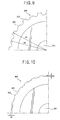
- FIG. 9 illustrates an enlarged partial view of a liquid crystal display panel cutting wheel according to a third embodiment of the present invention.
- FIG. 10 illustrates an enlarged partial view of a liquid crystal display panel cutting wheel according to a fourth embodiment of the present invention.
- FIG. 11 illustrates an enlarged view of a liquid crystal display panel cutting wheel in part according to a fifth embodiment of the present invention.
- FIG. 5 illustrates a perspective view of a cutting wheel for a liquid crystal display panel according to a first embodiment of the present invention.
- a cutting wheel for a liquid crystal display panel has a circular shape and includes a first cutting wheel 100 and a second cutting wheel 200 .
- Penetrating holes 101 and 201 are formed at centers of the first and second cutting wheels 100 and 200 to receive a support spindle (not shown). And, unevenly-shaped, or serrated first and second blades 102 and 202 are formed along edges of the first and second cutting wheels 100 and 200 , respectively. Protrusions of first and second blades 102 and 202 may also be evenly or unevenly spaced.
- the first and second cutting blades 102 and 202 according to the first embodiment of the present invention are preferably made of diamond, which has a hardness greater than that of generally used tungsten carbide, which will extend the endurance of the cutting blades.
- the first and second cutting wheels 100 and 200 can be formed individually to be bonded to a support spindle (not shown) through the penetrating holes 101 and 201 , or the cutting wheels 100 and 2000 can be built in one body, i.e., unitary.
- the rotating first and second blades 102 and 202 along edges of the first and second cutting wheels 100 and 200 come into close contact with the liquid crystal display panel of glass at a uniform pressure so as to form grooves having a predetermined depth.
- FIG. 6 illustrates an exemplary diagram of first and second grooves formed on a surface of a liquid crystal display panel using the first and second cutting wheels 100 and 200 according to the first embodiment of the present invention.
- first groove 151 is formed on a surface of a liquid crystal display panel 150 by first blades 102 of the first cutting wheel 100
- second groove 152 is formed on the surface of the liquid crystal display panel 150 by second blades 202 of the second cutting wheel 200 .
- the first and second grooves 151 and 152 are shown as a pair of parallel dotted lines. In practice, the first and second grooves 151 and 152 are about 300 ⁇ m apart.
- the first and second blades 102 and 202 are formed along the edges of the first and second cutting wheels 100 and 200 .
- the grooves are formed using a pair of the cutting wheels 100 and 200 . Hence, the cutting of the liquid crystal display panel can be carried out at a pressure lower than the case of using a single cutting wheel.
- the second blades 202 are able to form a normal groove on the surface of liquid crystal display panel.
- a groove can be formed on the liquid crystal display panel using the second blade 202 of the second cutting wheel 200 instead of replacing the first cutting wheel 100 , as in the related art.
- the cutting wheel for the liquid crystal display panel according to the first embodiment of the present invention has an extended endurance longer than that of the cutting wheel having the blade according to the related art.
- FIG. 7 illustrates a perspective view of first and second cutting wheels 100 and 200 , of which first and second blades 102 and 202 are staggered or offset with respect to each other, respectively, according to a second embodiment of the present invention.
- the offset of the first and second blades 102 and 202 may be at a predetermined angle.
- first and second blades 102 and 202 are arranged so that the blades of the respective wheels 100 and 200 are staggered or offset with respect to each other.
- First and second groves 151 and 152 also alternate with respect to each other on the surface of a liquid crystal display panel 150 . Cracks can be propagated well from the first and second grooves 151 and 152 .
- a groove can be formed on the liquid crystal display panel using the second blade 202 of the second cutting wheel 200 so as to extend the endurance of the cutting wheel.
- FIG. 9 illustrates an enlarged partial view of a liquid crystal display panel cutting wheel according to a third embodiment of the present invention.
- a circular cutting wheel 300 includes a penetrating hole 301 at a center to receive a support spindle (not shown), evenly-spaced first blades 302 are formed by grinding front and rear faces of the cutting wheel 300 along edges so that protrusions of the first blades 302 protrude from the center of the cutting wheel 300 at a first radius R 1 , and evenly-spaced second blades 303 alternating with the first blades 302 respectively so that protrusions of the second blades 303 protrude from the center of the cutting wheel 300 by a second radius R 2 .
- the first and second blades 302 and 303 may be unevenly spaced and/or unevenly shaped.
- the first and second blades 302 and 303 in FIG. 9 are preferably formed of diamond, which has a hardness greater than that of generally-used tungsten carbide.
- the first blades 302 protruding from the center of the cutting wheel 300 by the first radius R 1 are made to adhere closely to a liquid crystal display panel at a predetermined pressure and are rotated thereon, to form a groove having a predetermined uniform depth.
- the first blades 302 are abraded after grooves totaling 6000 m in length have been formed on the plurality of liquid crystal display panels such that a normal groove cannot be formed on the surface of the liquid crystal display panels.
- the second blades 303 protruding from the center of the cutting wheel 300 by the second radius R 2 are capable of forming the normal groove on the surface of the liquid crystal display panels.
- the normal groove can be formed on the liquid crystal display panel using the second blades 303 instead of replacing the cutting wheel 300 .
- the cutting wheel according to the third embodiment of the present invention has an extended endurance compared to that of the cutting wheel according to the related art, thereby extending the life of the cutting wheel.
- FIG. 10 illustrates an enlarged partial view of a liquid crystal display panel cutting wheel according to a fourth embodiment of the present invention.
- a circular cutting wheel 400 includes a penetrating hole 401 at a center to receive a support spindle (not shown), evenly-spaced first blades 402 formed by grinding front and rear faces of the cutting wheel along edges so as to have a first height H 1 from a perceived edge of the cutting wheel 400 , and evenly-spaced second blades 403 formed between the first blades 402 so as a second height H 2 .
- the first and second blades 402 and 403 may be unevenly shaped and may be unevenly spaced with respect to one another.
- the second blades 403 having the second height H 2 are capable of forming the normal groove on the surface of the liquid crystal display panel.
- the normal groove can be formed on the liquid crystal display panel using the second blades 403 instead of replacing the cutting wheel 400 .
- the cutting wheel according to the fourth embodiment of the present invention has an extended endurance compared to that of the cutting wheel according to the related art, thereby extending the life of the cutting wheel.
- FIG. 11 illustrates a perspective view of a liquid crystal display panel cutting wheel according to a fifth embodiment of the present invention.
- a first circular cutting wheel 500 includes a penetrating hole 501 at a center to receive a support spindle (not shown) and evenly-spaced first blades 502 formed by grinding front and rear faces of the first cutting wheel 500 along an edge to protrude from the center of the first cutting wheel 500 by a first radius R 1 and spaced apart from each other by a predetermined interval.
- a second circular cutting wheel 510 includes a penetrating hole 511 at a center to receive the support spindle and evenly-spaced second blades 512 formed by grinding front and rear faces of the second cutting wheel 510 along an edge to protrude from the center of the second cutting wheel 510 by a second radius R 2 and spaced apart from each other by a predetermined interval.
- the first and second blades 502 and 512 may be unevenly shaped and may be unevenly spaced with respect to each other.
- the second blades 512 of the second wheel 510 may be offset from the first blades 502 of the first wheel 500 , for example, by a predetermined angle.
- the first and second cutting wheels 500 and 510 are manufactured individually so as to be bonded to the support spindle through the penetrating holes 501 and 511 or can built in one body, i.e., be unitary.
- the second blades 512 are capable of forming the normal groove on the surface of the liquid crystal display panel.
- the normal groove can be formed on the liquid crystal display panel using the second blades 512 of the second cutting wheel 510 instead of replacing the first cutting wheel 500 .
- the cutting wheel for the liquid crystal display panel according to the fifth embodiment of the present invention has an extended endurance compared to that of the cutting wheel according to the related art, thereby extending the life of the cutting wheel.
- the cutting wheel for the liquid crystal display panel according to the first or second embodiment of the present invention includes a pair of the same-sized cutting wheels and the blades along the edges respectively, which can be operated under an improved pressure condition compared to the conventional devices.
- the cutting wheel for the liquid crystal display panel according to the first or second embodiment of the present invention is capable of forming a groove on the surface of the liquid crystal display panel continuously even if the blades of one of the cutting wheels are broken in part or particles are attached between the blades, thereby extending the life of the cutting wheel to improve a productivity as well as reduce a cost of purchasing the cutting wheel.
- the cutting wheel for the liquid crystal display panel according to the third, fourth, or fifth embodiment of the present invention has differentiated protruding heights of the blades formed along the edges of the circular cutting wheel, thereby extending the endurance of the cutting wheel compared to that of the related art. Therefore, the present invention extends the replacement time of the cutting wheel to improve productivity as well as reduce a cost of purchasing replacement cutting wheels.
Abstract
Description
Claims (5)
Applications Claiming Priority (4)
| Application Number | Priority Date | Filing Date | Title |
|---|---|---|---|
| KR1020020010311A KR100798319B1 (en) | 2002-02-26 | 2002-02-26 | Cutting wheel of liquid crystal display panel |
| KR2002-10311 | 2002-02-26 | ||
| KR2002-10312 | 2002-02-26 | ||
| KR1020020010312A KR20030070782A (en) | 2002-02-26 | 2002-02-26 | Cutting wheel of liquid crystal display panel |
Publications (2)
| Publication Number | Publication Date |
|---|---|
| US20030159297A1 US20030159297A1 (en) | 2003-08-28 |
| US8074551B2 true US8074551B2 (en) | 2011-12-13 |
Family
ID=27759809
Family Applications (1)
| Application Number | Title | Priority Date | Filing Date |
|---|---|---|---|
| US10/184,082 Expired - Fee Related US8074551B2 (en) | 2002-02-26 | 2002-06-28 | Cutting wheel for liquid crystal display panel |
Country Status (3)
| Country | Link |
|---|---|
| US (1) | US8074551B2 (en) |
| JP (1) | JP4126594B2 (en) |
| CN (1) | CN100493793C (en) |
Cited By (2)
| Publication number | Priority date | Publication date | Assignee | Title |
|---|---|---|---|---|
| US20130291703A1 (en) * | 2008-05-28 | 2013-11-07 | Mueller Martini Holding Ag | Device for forming a groove |
| US20180141229A1 (en) * | 2016-11-22 | 2018-05-24 | Xerox Corporation | Sequential die cut and slitting for improved collation |
Families Citing this family (17)
| Publication number | Priority date | Publication date | Assignee | Title |
|---|---|---|---|---|
| JP4038431B2 (en) * | 2001-03-16 | 2008-01-23 | 三星ダイヤモンド工業株式会社 | Scribing method, cutter wheel, scribing apparatus using the cutter wheel, and cutter wheel manufacturing apparatus for manufacturing the cutter wheel |
| WO2004048058A1 (en) * | 2002-11-22 | 2004-06-10 | Mitsuboshi Diamond Industrial Co.,Ltd. | Method for dividing substrate and method for manufacturing substrate using such method |
| US7694422B2 (en) * | 2006-10-17 | 2010-04-13 | Ed Vaes | Utility knife |
| EP2121260B1 (en) * | 2007-01-19 | 2014-02-12 | Awin Diamond Technology Corporation | Cutting disk for forming a scribed line and method of manufacturing the same |
| WO2009034759A1 (en) * | 2007-09-13 | 2009-03-19 | Sharp Kabushiki Kaisha | Cutter wheel |
| DE102007045383A1 (en) * | 2007-09-22 | 2008-07-17 | Bohle Ag | Production of cutting wheels for producing notched predetermined breaking points comprises forming a toothed structure using a laser beam to partially remove the peripheral region of the wheel in a specified region |
| DE202007013307U1 (en) * | 2007-09-22 | 2008-04-24 | Bohle Ag | cutting wheel |
| DE202007013306U1 (en) * | 2007-09-22 | 2008-04-24 | Bohle Ag | cutting wheel |
| KR20110013510A (en) * | 2008-06-05 | 2011-02-09 | 미쓰보시 다이야몬도 고교 가부시키가이샤 | Scribing wheel and method for scribing brittle material substrate |
| KR101138044B1 (en) | 2009-07-17 | 2012-04-23 | 이화다이아몬드공업 주식회사 | Scribing cutter having deposition layer and method of fabrication the same |
| KR101174876B1 (en) * | 2010-01-19 | 2012-08-17 | 삼성디스플레이 주식회사 | Cutting wheel for glass substrate |
| CN102211230A (en) * | 2010-04-06 | 2011-10-12 | 陈重光 | Saw bit capable of bidirectionally sawing |
| US20130112058A1 (en) * | 2011-11-09 | 2013-05-09 | James William Brown | Methods of manufacturing a glass substrate |
| CN103085106B (en) * | 2013-02-01 | 2015-09-30 | 四川虹视显示技术有限公司 | Oled substrate diced system |
| CN103316869A (en) * | 2013-06-26 | 2013-09-25 | 上海和辉光电有限公司 | Mechanism and method for automatically cleaning cutting wheel |
| EP2871034A1 (en) * | 2013-11-12 | 2015-05-13 | Nederlandse Organisatie voor toegepast- natuurwetenschappelijk onderzoek TNO | Cutting tool and cutting method for laminates. |
| KR102509796B1 (en) * | 2022-12-08 | 2023-03-14 | 유한회사 케이조선앤특수선 | screw foreign object removal device |
Citations (126)
| Publication number | Priority date | Publication date | Assignee | Title |
|---|---|---|---|---|
| US2762954A (en) * | 1950-09-09 | 1956-09-11 | Sylvania Electric Prod | Method for assembling transistors |
| JPS5165656A (en) | 1974-12-04 | 1976-06-07 | Shinshu Seiki Kk | |
| US3978580A (en) | 1973-06-28 | 1976-09-07 | Hughes Aircraft Company | Method of fabricating a liquid crystal display |
| US4094058A (en) | 1976-07-23 | 1978-06-13 | Omron Tateisi Electronics Co. | Method of manufacture of liquid crystal displays |
| JPS5738414A (en) | 1980-08-20 | 1982-03-03 | Showa Denko Kk | Spacer for display panel |
| JPS5788428A (en) | 1980-11-20 | 1982-06-02 | Ricoh Elemex Corp | Manufacture of liquid crystal display body device |
| JPS5827126A (en) | 1981-08-11 | 1983-02-17 | Nec Corp | Production of liquid crystal display panel |
| JPS5957221A (en) | 1982-09-28 | 1984-04-02 | Asahi Glass Co Ltd | Production of display element |
| JPS59195222A (en) | 1983-04-19 | 1984-11-06 | Matsushita Electric Ind Co Ltd | Manufacture of liquid-crystal panel |
| JPS60111221A (en) | 1983-11-19 | 1985-06-17 | Nippon Denso Co Ltd | Method and device for charging liquid crystal |
| JPS60164723A (en) | 1984-02-07 | 1985-08-27 | Seiko Instr & Electronics Ltd | Liquid crystal display device |
| JPS60217343A (en) | 1984-04-13 | 1985-10-30 | Matsushita Electric Ind Co Ltd | Liquid crystal display device and its preparation |
| JPS617822A (en) | 1984-06-22 | 1986-01-14 | Canon Inc | Production of liquid crystal element |
| JPS6155625A (en) | 1984-08-24 | 1986-03-20 | Nippon Denso Co Ltd | Manufacture of liquid crystal element |
| JPS6254225A (en) | 1985-07-15 | 1987-03-09 | Semiconductor Energy Lab Co Ltd | Manufacturing method for liquid crystal display |
| JPS6254228A (en) | 1985-07-15 | 1987-03-09 | Semiconductor Energy Lab Co Ltd | Manufacturing method for liquid crystal display |
| JPS6254229A (en) | 1985-07-15 | 1987-03-09 | Semiconductor Energy Lab Co Ltd | Manufacturing method for liquid crystal display |
| US4653864A (en) | 1986-02-26 | 1987-03-31 | Ovonic Imaging Systems, Inc. | Liquid crystal matrix display having improved spacers and method of making same |
| JPS6289025A (en) | 1985-10-15 | 1987-04-23 | Matsushita Electric Ind Co Ltd | Liquid crystal display panel and its production |
| JPS6290622A (en) | 1985-10-17 | 1987-04-25 | Seiko Epson Corp | Liquid crystal display device |
| US4691995A (en) | 1985-07-15 | 1987-09-08 | Semiconductor Energy Laboratory Co., Ltd. | Liquid crystal filling device |
| JPS62205319A (en) | 1986-03-06 | 1987-09-09 | Canon Inc | Ferroelectric liquid crystal element |
| JPS63110425A (en) | 1986-10-29 | 1988-05-14 | Toppan Printing Co Ltd | Cell for sealing liquid crystal |
| JPS63109413A (en) | 1986-10-27 | 1988-05-14 | Fujitsu Ltd | Production of liquid crystal display |
| JPS63128315A (en) | 1986-11-19 | 1988-05-31 | Victor Co Of Japan Ltd | Liquid crystal display element |
| US4775225A (en) | 1985-05-16 | 1988-10-04 | Canon Kabushiki Kaisha | Liquid crystal device having pillar spacers with small base periphery width in direction perpendicular to orientation treatment |
| JPS63311233A (en) | 1987-06-12 | 1988-12-20 | Toyota Motor Corp | Liquid crystal cell |
| JPH039549A (en) | 1989-05-16 | 1991-01-17 | Motorola Inc | Composite integrated storage device |
| US5024026A (en) * | 1989-07-17 | 1991-06-18 | American Saw & Mfg. Company | Segmental grinding wheel |
| JPH0536426A (en) | 1991-07-31 | 1993-02-12 | Mitsubishi Heavy Ind Ltd | Solid electrolytic fuel cell |
| JPH0536425A (en) | 1991-02-12 | 1993-02-12 | Tokyo Electric Power Co Inc:The | Alloy separator for solid electrolytic fuel cell and manufacture of the same |
| US5197453A (en) * | 1992-08-28 | 1993-03-30 | Sanders Saws, Inc. | Two-tier groove cutting circular saw blade with multiple core assembly |
| JPH05107533A (en) | 1991-10-16 | 1993-04-30 | Shinetsu Eng Kk | Method and device for sticking glass substrate for liquid crystal display plate |
| JPH05127179A (en) | 1991-11-01 | 1993-05-25 | Ricoh Co Ltd | Production of liquid crystal display element |
| JPH05154923A (en) | 1991-12-06 | 1993-06-22 | Hitachi Ltd | Substrate assembling device |
| US5247377A (en) | 1988-07-23 | 1993-09-21 | Rohm Gmbh Chemische Fabrik | Process for producing anisotropic liquid crystal layers on a substrate |
| JPH05265011A (en) | 1992-03-19 | 1993-10-15 | Seiko Instr Inc | Production of liquid crystal display element |
| JPH05281562A (en) | 1992-04-01 | 1993-10-29 | Matsushita Electric Ind Co Ltd | Manufacture of liquid crystal panel |
| JPH05281557A (en) | 1992-04-01 | 1993-10-29 | Matsushita Electric Ind Co Ltd | Manufacture of liquid crystal panel |
| US5263888A (en) | 1992-02-20 | 1993-11-23 | Matsushita Electric Industrial Co., Ltd. | Method of manufacture of liquid crystal display panel |
| JPH0618829A (en) | 1992-06-30 | 1994-01-28 | Shinetsu Eng Kk | Laminating device for glass substrate for liquid crystal display board |
| JPH0651256A (en) | 1992-07-30 | 1994-02-25 | Matsushita Electric Ind Co Ltd | Device for discharging liquid crystal |
| JPH0664229A (en) | 1992-08-24 | 1994-03-08 | Toshiba Corp | Optical printing head |
| JPH06148657A (en) | 1992-11-06 | 1994-05-27 | Matsushita Electric Ind Co Ltd | Method and device for manufacturing cell for liquid crystal display |
| JPH06160871A (en) | 1992-11-26 | 1994-06-07 | Matsushita Electric Ind Co Ltd | Liquid crystal display panel and its production |
| JPH06194637A (en) | 1992-12-24 | 1994-07-15 | Shinetsu Eng Kk | Method for sticking glass substrate for liquid crystal display plate |
| JPH06235925A (en) | 1993-02-10 | 1994-08-23 | Matsushita Electric Ind Co Ltd | Manufacture of liquid crystal display element |
| JPH06265915A (en) | 1993-03-12 | 1994-09-22 | Matsushita Electric Ind Co Ltd | Discharge device for filling liquid crystal |
| JPH06313870A (en) | 1993-04-28 | 1994-11-08 | Hitachi Ltd | Substrate assembly device |
| US5379139A (en) | 1986-08-20 | 1995-01-03 | Semiconductor Energy Laboratory Co., Ltd. | Liquid crystal device and method for manufacturing same with spacers formed by photolithography |
| JPH0784268A (en) | 1993-09-13 | 1995-03-31 | Hitachi Ltd | Method for plotting sealing material |
| US5406989A (en) | 1993-10-12 | 1995-04-18 | Ayumi Industry Co., Ltd. | Method and dispenser for filling liquid crystal into LCD cell |
| JPH07128674A (en) | 1993-11-05 | 1995-05-19 | Matsushita Electric Ind Co Ltd | Production of liquid crystal display element |
| JPH07181507A (en) | 1993-12-21 | 1995-07-21 | Canon Inc | Liquid crystal display device and information transmission device having the liquid crystal display device |
| JPH07275771A (en) | 1994-04-11 | 1995-10-24 | Hitachi Techno Eng Co Ltd | Coating applicator for paste |
| JPH07275770A (en) | 1994-04-06 | 1995-10-24 | Hitachi Techno Eng Co Ltd | Paste applicator |
| US5499128A (en) | 1993-03-15 | 1996-03-12 | Kabushiki Kaisha Toshiba | Liquid crystal display device with acrylic polymer spacers and method of manufacturing the same |
| JPH0876133A (en) | 1994-09-02 | 1996-03-22 | Shinetsu Eng Kk | Surface plate structure in laminating device for glass substrate for liquid crystal display plate |
| JPH0895066A (en) | 1994-09-27 | 1996-04-12 | Matsushita Electric Ind Co Ltd | Manufacture of liquid crystal element and device thereof |
| JPH08101395A (en) | 1994-09-30 | 1996-04-16 | Matsushita Electric Ind Co Ltd | Production of liquid crystal display element |
| US5507323A (en) | 1993-10-12 | 1996-04-16 | Fujitsu Limited | Method and dispenser for filling liquid crystal into LCD cell |
| JPH08106101A (en) | 1994-10-06 | 1996-04-23 | Fujitsu Ltd | Production of liquid crystal display panel |
| JPH08110504A (en) | 1994-10-13 | 1996-04-30 | Shinetsu Eng Kk | Heater of glass substrate for liquid crystal display |
| JPH08136937A (en) | 1994-11-09 | 1996-05-31 | Shinetsu Eng Kk | Method for pressurizing and heating glass substrate for liquid crystal display plate and device therefor |
| JPH08171094A (en) | 1994-12-19 | 1996-07-02 | Nippon Soken Inc | Liquid crystal injecting method and liquid crystal injecting device to liquid crystal display device |
| JPH08173874A (en) | 1994-12-26 | 1996-07-09 | Hitachi Techno Eng Co Ltd | Paste coater |
| JPH08190099A (en) | 1995-01-11 | 1996-07-23 | Fujitsu Ltd | Production of liquid crystal display device and apparatus for producing liquid crystal display device |
| US5539545A (en) | 1993-05-18 | 1996-07-23 | Semiconductor Energy Laboratory Co., Ltd. | Method of making LCD in which resin columns are cured and the liquid crystal is reoriented |
| US5548429A (en) | 1993-06-14 | 1996-08-20 | Canon Kabushiki Kaisha | Process for producing liquid crystal device whereby curing the sealant takes place after pre-baking the substrates |
| JPH08240807A (en) | 1995-03-06 | 1996-09-17 | Fujitsu Ltd | Method for sealing liquid crystal display panel |
| US5569285A (en) * | 1994-11-02 | 1996-10-29 | Webb; Nicholas J. | Scalpel with rotary depth guard |
| US5579754A (en) * | 1990-04-27 | 1996-12-03 | Chiuminatta; Edward | Apparatus and method for cutting unhardened concrete |
| JPH091026A (en) | 1995-06-23 | 1997-01-07 | Hitachi Techno Eng Co Ltd | Paste coating machine |
| JPH095762A (en) | 1995-06-20 | 1997-01-10 | Matsushita Electric Ind Co Ltd | Production of liquid crystal panel |
| JPH0926578A (en) | 1995-07-10 | 1997-01-28 | Fujitsu Ltd | Liquid crystal display panel and manufacture thereof |
| JPH0961829A (en) | 1995-08-21 | 1997-03-07 | Matsushita Electric Ind Co Ltd | Production of liquid crystal display element |
| US5642214A (en) | 1991-07-19 | 1997-06-24 | Sharp Kabushiki Kaisha | Optical modulating element and electronic apparatus using it |
| JPH09311340A (en) | 1996-05-21 | 1997-12-02 | Matsushita Electric Ind Co Ltd | Manufacture of liquid crystal display device |
| US5742370A (en) | 1996-09-12 | 1998-04-21 | Korea Institute Of Science And Technology | Fabrication method for liquid crystal alignment layer by magnetic field treatment |
| US5757451A (en) | 1995-09-08 | 1998-05-26 | Kabushiki Kaisha Toshiba | Liquid crystal display device spacers formed from stacked color layers |
| US5852484A (en) | 1994-09-26 | 1998-12-22 | Matsushita Electric Industrial Co., Ltd. | Liquid crystal display panel and method and device for manufacturing the same |
| US5861932A (en) | 1997-03-31 | 1999-01-19 | Denso Corporation | Liquid crystal cell and its manufacturing method |
| US5875922A (en) | 1997-10-10 | 1999-03-02 | Nordson Corporation | Apparatus for dispensing an adhesive |
| US5907984A (en) * | 1995-04-19 | 1999-06-01 | Cutting Edge Inc. | Parallel cutting assembly for cutting sheet material |
| US5952676A (en) | 1986-08-20 | 1999-09-14 | Semiconductor Energy Laboratory Co., Ltd. | Liquid crystal device and method for manufacturing same with spacers formed by photolithography |
| US5952678A (en) | 1995-01-23 | 1999-09-14 | Mitsubishi Denki Kabushiki Kaisha | SRAM cell with no PN junction between driver and load transistors and method of manufacturing the same |
| US5956112A (en) | 1995-10-02 | 1999-09-21 | Sharp Kabushiki Kaisha | Liquid crystal display device and method for manufacturing the same |
| US6001203A (en) | 1995-03-01 | 1999-12-14 | Matsushita Electric Industrial Co., Ltd. | Production process of liquid crystal display panel, seal material for liquid crystal cell and liquid crystal display |
| US6011609A (en) | 1996-10-05 | 2000-01-04 | Samsung Electronics Co., Ltd. | Method of manufacturing LCD by dropping liquid crystals on a substrate and then pressing the substrates |
| US6016181A (en) | 1996-11-07 | 2000-01-18 | Sharp Kabushiki Kaisha | Liquid crystal device having column spacers with portion on each of the spacers for reflecting or absorbing visible light and method for fabricating the same |
| US6016178A (en) | 1996-09-13 | 2000-01-18 | Sony Corporation | Reflective guest-host liquid-crystal display device |
| JP2000029035A (en) | 1998-07-09 | 2000-01-28 | Minolta Co Ltd | Liquid crystal element and its manufacture |
| US6055035A (en) | 1998-05-11 | 2000-04-25 | International Business Machines Corporation | Method and apparatus for filling liquid crystal display (LCD) panels |
| EP1003066A1 (en) | 1998-11-16 | 2000-05-24 | Matsushita Electric Industrial Co., Ltd. | Method of manufacturing liquid crystal display devices |
| US6163357A (en) | 1996-09-26 | 2000-12-19 | Kabushiki Kaisha Toshiba | Liquid crystal display device having the driving circuit disposed in the seal area, with different spacer density in driving circuit area than display area |
| US6219126B1 (en) | 1998-11-20 | 2001-04-17 | International Business Machines Corporation | Panel assembly for liquid crystal displays having a barrier fillet and an adhesive fillet in the periphery |
| JP2001117105A (en) | 1999-10-18 | 2001-04-27 | Toshiba Corp | Method of manufacturing for liquid crystal display device |
| US6226067B1 (en) | 1997-10-03 | 2001-05-01 | Minolta Co., Ltd. | Liquid crystal device having spacers and manufacturing method thereof |
| JP2001133794A (en) | 1999-11-01 | 2001-05-18 | Kyoritsu Kagaku Sangyo Kk | Sealing agent for dropping process of lcd panel |
| US6236445B1 (en) | 1996-02-22 | 2001-05-22 | Hughes Electronics Corporation | Method for making topographic projections |
| JP2001142074A (en) | 1999-11-10 | 2001-05-25 | Hitachi Ltd | Liquid crystal display device |
| JP2001147437A (en) | 1999-11-19 | 2001-05-29 | Nec Corp | Liquid crystal display panel and method of producing the same |
| JP2001154211A (en) | 1999-11-30 | 2001-06-08 | Hitachi Ltd | Liquid crystal panel and its manufacturing method |
| US20010021000A1 (en) | 2000-02-02 | 2001-09-13 | Norihiko Egami | Apparatus and method for manufacturing liquid crystal display |
| JP2001255542A (en) | 2000-03-14 | 2001-09-21 | Sharp Corp | Method and device for laminating substrate and method and device for manufacturing liquid crystal display device |
| JP2001264782A (en) | 2000-03-16 | 2001-09-26 | Ayumi Kogyo Kk | Method of filling gap of flat panel substrate with viscous liquid material |
| US6304306B1 (en) | 1995-02-17 | 2001-10-16 | Sharp Kabushiki Kaisha | Liquid crystal display device and method for producing the same |
| JP2001330840A (en) | 2000-05-18 | 2001-11-30 | Toshiba Corp | Method for manufacturing liquid crystal display element |
| JP2001356354A (en) | 2000-06-13 | 2001-12-26 | Matsushita Electric Ind Co Ltd | Method for manufacturing liquid crystal display device |
| US6337730B1 (en) | 1998-06-02 | 2002-01-08 | Denso Corporation | Non-uniformly-rigid barrier wall spacers used to correct problems caused by thermal contraction of smectic liquid crystal material |
| JP2002014360A (en) | 2000-06-29 | 2002-01-18 | Matsushita Electric Ind Co Ltd | Method and device for manufacturing liquid crystal panel |
| JP2002023176A (en) | 2000-07-05 | 2002-01-23 | Seiko Epson Corp | Liquid crystal filling system and method for filling liquid crystal |
| JP2002049045A (en) | 2000-08-03 | 2002-02-15 | Nec Corp | Method for manufacturing liquid crystal display panel |
| JP2002080321A (en) | 2000-06-20 | 2002-03-19 | Kyowa Hakko Kogyo Co Ltd | Cosmetic |
| JP2002082340A (en) | 2000-09-08 | 2002-03-22 | Fuji Xerox Co Ltd | Method for manufacturing flat panel display |
| JP2002090759A (en) | 2000-09-18 | 2002-03-27 | Sharp Corp | Apparatus and method for manufacturing liquid crystal display element |
| JP2002090760A (en) | 2000-09-12 | 2002-03-27 | Matsushita Electric Ind Co Ltd | Apparatus and method for manufacturing liquid crystal display panel |
| JP2002107740A (en) | 2000-09-28 | 2002-04-10 | Sharp Corp | Method and device for manufacturing liquid crystal display panel |
| JP2002122872A (en) | 2000-10-12 | 2002-04-26 | Hitachi Ltd | Liquid crystal display device and method of manufacturing the same |
| JP2002122873A (en) | 2000-10-13 | 2002-04-26 | Stanley Electric Co Ltd | Method of manufacturing liquid crystal display device |
| US6390086B1 (en) * | 2000-08-25 | 2002-05-21 | Louis M. Collins | Mobile concrete saw |
| US6414733B1 (en) | 1999-02-08 | 2002-07-02 | Dai Nippon Printing Co., Ltd. | Color liquid crystal display with a shielding member being arranged between sealing member and display zone |
| US6413150B1 (en) * | 1999-05-27 | 2002-07-02 | Texas Instruments Incorporated | Dual dicing saw blade assembly and process for separating devices arrayed a substrate |
| JP2002202512A (en) | 2000-12-28 | 2002-07-19 | Toshiba Corp | Liquid crystal display device and method of manufacturing for the same |
| JP2002202514A (en) | 2000-12-28 | 2002-07-19 | Matsushita Electric Ind Co Ltd | Liquid crystal panel, and method and manufacturing apparatus for manufacturing the same |
| JP2002214626A (en) | 2001-01-17 | 2002-07-31 | Toshiba Corp | Manufacturing method and sealing material for liquid crystal display |
Family Cites Families (1)
| Publication number | Priority date | Publication date | Assignee | Title |
|---|---|---|---|---|
| US6061181A (en) * | 1997-06-09 | 2000-05-09 | Fereidooni; Fred | Nontracking light converger |
-
2002
- 2002-06-28 US US10/184,082 patent/US8074551B2/en not_active Expired - Fee Related
- 2002-07-24 JP JP2002214967A patent/JP4126594B2/en not_active Expired - Fee Related
- 2002-09-03 CN CNB021319642A patent/CN100493793C/en not_active Expired - Fee Related
Patent Citations (130)
| Publication number | Priority date | Publication date | Assignee | Title |
|---|---|---|---|---|
| US2762954A (en) * | 1950-09-09 | 1956-09-11 | Sylvania Electric Prod | Method for assembling transistors |
| US3978580A (en) | 1973-06-28 | 1976-09-07 | Hughes Aircraft Company | Method of fabricating a liquid crystal display |
| JPS5165656A (en) | 1974-12-04 | 1976-06-07 | Shinshu Seiki Kk | |
| US4094058A (en) | 1976-07-23 | 1978-06-13 | Omron Tateisi Electronics Co. | Method of manufacture of liquid crystal displays |
| JPS5738414A (en) | 1980-08-20 | 1982-03-03 | Showa Denko Kk | Spacer for display panel |
| JPS5788428A (en) | 1980-11-20 | 1982-06-02 | Ricoh Elemex Corp | Manufacture of liquid crystal display body device |
| JPS5827126A (en) | 1981-08-11 | 1983-02-17 | Nec Corp | Production of liquid crystal display panel |
| JPS5957221A (en) | 1982-09-28 | 1984-04-02 | Asahi Glass Co Ltd | Production of display element |
| JPS59195222A (en) | 1983-04-19 | 1984-11-06 | Matsushita Electric Ind Co Ltd | Manufacture of liquid-crystal panel |
| JPS60111221A (en) | 1983-11-19 | 1985-06-17 | Nippon Denso Co Ltd | Method and device for charging liquid crystal |
| JPS60164723A (en) | 1984-02-07 | 1985-08-27 | Seiko Instr & Electronics Ltd | Liquid crystal display device |
| JPS60217343A (en) | 1984-04-13 | 1985-10-30 | Matsushita Electric Ind Co Ltd | Liquid crystal display device and its preparation |
| JPS617822A (en) | 1984-06-22 | 1986-01-14 | Canon Inc | Production of liquid crystal element |
| JPS6155625A (en) | 1984-08-24 | 1986-03-20 | Nippon Denso Co Ltd | Manufacture of liquid crystal element |
| US4775225A (en) | 1985-05-16 | 1988-10-04 | Canon Kabushiki Kaisha | Liquid crystal device having pillar spacers with small base periphery width in direction perpendicular to orientation treatment |
| US4691995A (en) | 1985-07-15 | 1987-09-08 | Semiconductor Energy Laboratory Co., Ltd. | Liquid crystal filling device |
| JPS6254228A (en) | 1985-07-15 | 1987-03-09 | Semiconductor Energy Lab Co Ltd | Manufacturing method for liquid crystal display |
| JPS6254225A (en) | 1985-07-15 | 1987-03-09 | Semiconductor Energy Lab Co Ltd | Manufacturing method for liquid crystal display |
| JPS6254229A (en) | 1985-07-15 | 1987-03-09 | Semiconductor Energy Lab Co Ltd | Manufacturing method for liquid crystal display |
| JPS6289025A (en) | 1985-10-15 | 1987-04-23 | Matsushita Electric Ind Co Ltd | Liquid crystal display panel and its production |
| JPS6290622A (en) | 1985-10-17 | 1987-04-25 | Seiko Epson Corp | Liquid crystal display device |
| US4653864A (en) | 1986-02-26 | 1987-03-31 | Ovonic Imaging Systems, Inc. | Liquid crystal matrix display having improved spacers and method of making same |
| JPS62205319A (en) | 1986-03-06 | 1987-09-09 | Canon Inc | Ferroelectric liquid crystal element |
| US5379139A (en) | 1986-08-20 | 1995-01-03 | Semiconductor Energy Laboratory Co., Ltd. | Liquid crystal device and method for manufacturing same with spacers formed by photolithography |
| US5952676A (en) | 1986-08-20 | 1999-09-14 | Semiconductor Energy Laboratory Co., Ltd. | Liquid crystal device and method for manufacturing same with spacers formed by photolithography |
| JPS63109413A (en) | 1986-10-27 | 1988-05-14 | Fujitsu Ltd | Production of liquid crystal display |
| JPS63110425A (en) | 1986-10-29 | 1988-05-14 | Toppan Printing Co Ltd | Cell for sealing liquid crystal |
| JPS63128315A (en) | 1986-11-19 | 1988-05-31 | Victor Co Of Japan Ltd | Liquid crystal display element |
| JPS63311233A (en) | 1987-06-12 | 1988-12-20 | Toyota Motor Corp | Liquid crystal cell |
| US5247377A (en) | 1988-07-23 | 1993-09-21 | Rohm Gmbh Chemische Fabrik | Process for producing anisotropic liquid crystal layers on a substrate |
| JPH039549A (en) | 1989-05-16 | 1991-01-17 | Motorola Inc | Composite integrated storage device |
| US5024026A (en) * | 1989-07-17 | 1991-06-18 | American Saw & Mfg. Company | Segmental grinding wheel |
| US5579754A (en) * | 1990-04-27 | 1996-12-03 | Chiuminatta; Edward | Apparatus and method for cutting unhardened concrete |
| JPH0536425A (en) | 1991-02-12 | 1993-02-12 | Tokyo Electric Power Co Inc:The | Alloy separator for solid electrolytic fuel cell and manufacture of the same |
| US5642214A (en) | 1991-07-19 | 1997-06-24 | Sharp Kabushiki Kaisha | Optical modulating element and electronic apparatus using it |
| JPH0536426A (en) | 1991-07-31 | 1993-02-12 | Mitsubishi Heavy Ind Ltd | Solid electrolytic fuel cell |
| JPH05107533A (en) | 1991-10-16 | 1993-04-30 | Shinetsu Eng Kk | Method and device for sticking glass substrate for liquid crystal display plate |
| JPH05127179A (en) | 1991-11-01 | 1993-05-25 | Ricoh Co Ltd | Production of liquid crystal display element |
| JPH05154923A (en) | 1991-12-06 | 1993-06-22 | Hitachi Ltd | Substrate assembling device |
| US5263888A (en) | 1992-02-20 | 1993-11-23 | Matsushita Electric Industrial Co., Ltd. | Method of manufacture of liquid crystal display panel |
| JPH05265011A (en) | 1992-03-19 | 1993-10-15 | Seiko Instr Inc | Production of liquid crystal display element |
| JPH05281562A (en) | 1992-04-01 | 1993-10-29 | Matsushita Electric Ind Co Ltd | Manufacture of liquid crystal panel |
| JPH05281557A (en) | 1992-04-01 | 1993-10-29 | Matsushita Electric Ind Co Ltd | Manufacture of liquid crystal panel |
| US5511591A (en) | 1992-04-13 | 1996-04-30 | Fujitsu Limited | Method and dispenser for filling liquid crystal into LCD cell |
| JPH0618829A (en) | 1992-06-30 | 1994-01-28 | Shinetsu Eng Kk | Laminating device for glass substrate for liquid crystal display board |
| JPH0651256A (en) | 1992-07-30 | 1994-02-25 | Matsushita Electric Ind Co Ltd | Device for discharging liquid crystal |
| JPH0664229A (en) | 1992-08-24 | 1994-03-08 | Toshiba Corp | Optical printing head |
| US5197453A (en) * | 1992-08-28 | 1993-03-30 | Sanders Saws, Inc. | Two-tier groove cutting circular saw blade with multiple core assembly |
| JPH06148657A (en) | 1992-11-06 | 1994-05-27 | Matsushita Electric Ind Co Ltd | Method and device for manufacturing cell for liquid crystal display |
| JPH06160871A (en) | 1992-11-26 | 1994-06-07 | Matsushita Electric Ind Co Ltd | Liquid crystal display panel and its production |
| JPH06194637A (en) | 1992-12-24 | 1994-07-15 | Shinetsu Eng Kk | Method for sticking glass substrate for liquid crystal display plate |
| JPH06235925A (en) | 1993-02-10 | 1994-08-23 | Matsushita Electric Ind Co Ltd | Manufacture of liquid crystal display element |
| JPH06265915A (en) | 1993-03-12 | 1994-09-22 | Matsushita Electric Ind Co Ltd | Discharge device for filling liquid crystal |
| US5499128A (en) | 1993-03-15 | 1996-03-12 | Kabushiki Kaisha Toshiba | Liquid crystal display device with acrylic polymer spacers and method of manufacturing the same |
| JPH06313870A (en) | 1993-04-28 | 1994-11-08 | Hitachi Ltd | Substrate assembly device |
| US5539545A (en) | 1993-05-18 | 1996-07-23 | Semiconductor Energy Laboratory Co., Ltd. | Method of making LCD in which resin columns are cured and the liquid crystal is reoriented |
| US5680189A (en) | 1993-05-18 | 1997-10-21 | Semiconductor Energy Laboratory Co., Ltd. | LCD columnar spacers made of a hydrophilic resin and LCD orientation film having a certain surface tension or alignment capability |
| US5548429A (en) | 1993-06-14 | 1996-08-20 | Canon Kabushiki Kaisha | Process for producing liquid crystal device whereby curing the sealant takes place after pre-baking the substrates |
| JPH0784268A (en) | 1993-09-13 | 1995-03-31 | Hitachi Ltd | Method for plotting sealing material |
| US5507323A (en) | 1993-10-12 | 1996-04-16 | Fujitsu Limited | Method and dispenser for filling liquid crystal into LCD cell |
| US5406989A (en) | 1993-10-12 | 1995-04-18 | Ayumi Industry Co., Ltd. | Method and dispenser for filling liquid crystal into LCD cell |
| JPH07128674A (en) | 1993-11-05 | 1995-05-19 | Matsushita Electric Ind Co Ltd | Production of liquid crystal display element |
| JPH07181507A (en) | 1993-12-21 | 1995-07-21 | Canon Inc | Liquid crystal display device and information transmission device having the liquid crystal display device |
| JPH07275770A (en) | 1994-04-06 | 1995-10-24 | Hitachi Techno Eng Co Ltd | Paste applicator |
| JPH07275771A (en) | 1994-04-11 | 1995-10-24 | Hitachi Techno Eng Co Ltd | Coating applicator for paste |
| JPH0876133A (en) | 1994-09-02 | 1996-03-22 | Shinetsu Eng Kk | Surface plate structure in laminating device for glass substrate for liquid crystal display plate |
| US5854664A (en) | 1994-09-26 | 1998-12-29 | Matsushita Electric Industrial Co., Ltd. | Liquid crystal display panel and method and device for manufacturing the same |
| US5852484A (en) | 1994-09-26 | 1998-12-22 | Matsushita Electric Industrial Co., Ltd. | Liquid crystal display panel and method and device for manufacturing the same |
| JPH0895066A (en) | 1994-09-27 | 1996-04-12 | Matsushita Electric Ind Co Ltd | Manufacture of liquid crystal element and device thereof |
| JPH08101395A (en) | 1994-09-30 | 1996-04-16 | Matsushita Electric Ind Co Ltd | Production of liquid crystal display element |
| JPH08106101A (en) | 1994-10-06 | 1996-04-23 | Fujitsu Ltd | Production of liquid crystal display panel |
| JPH08110504A (en) | 1994-10-13 | 1996-04-30 | Shinetsu Eng Kk | Heater of glass substrate for liquid crystal display |
| US5569285A (en) * | 1994-11-02 | 1996-10-29 | Webb; Nicholas J. | Scalpel with rotary depth guard |
| JPH08136937A (en) | 1994-11-09 | 1996-05-31 | Shinetsu Eng Kk | Method for pressurizing and heating glass substrate for liquid crystal display plate and device therefor |
| JPH08171094A (en) | 1994-12-19 | 1996-07-02 | Nippon Soken Inc | Liquid crystal injecting method and liquid crystal injecting device to liquid crystal display device |
| JPH08173874A (en) | 1994-12-26 | 1996-07-09 | Hitachi Techno Eng Co Ltd | Paste coater |
| JPH08190099A (en) | 1995-01-11 | 1996-07-23 | Fujitsu Ltd | Production of liquid crystal display device and apparatus for producing liquid crystal display device |
| US5952678A (en) | 1995-01-23 | 1999-09-14 | Mitsubishi Denki Kabushiki Kaisha | SRAM cell with no PN junction between driver and load transistors and method of manufacturing the same |
| US6304306B1 (en) | 1995-02-17 | 2001-10-16 | Sharp Kabushiki Kaisha | Liquid crystal display device and method for producing the same |
| US6001203A (en) | 1995-03-01 | 1999-12-14 | Matsushita Electric Industrial Co., Ltd. | Production process of liquid crystal display panel, seal material for liquid crystal cell and liquid crystal display |
| JPH08240807A (en) | 1995-03-06 | 1996-09-17 | Fujitsu Ltd | Method for sealing liquid crystal display panel |
| US5907984A (en) * | 1995-04-19 | 1999-06-01 | Cutting Edge Inc. | Parallel cutting assembly for cutting sheet material |
| JPH095762A (en) | 1995-06-20 | 1997-01-10 | Matsushita Electric Ind Co Ltd | Production of liquid crystal panel |
| JPH091026A (en) | 1995-06-23 | 1997-01-07 | Hitachi Techno Eng Co Ltd | Paste coating machine |
| JPH0926578A (en) | 1995-07-10 | 1997-01-28 | Fujitsu Ltd | Liquid crystal display panel and manufacture thereof |
| JPH0961829A (en) | 1995-08-21 | 1997-03-07 | Matsushita Electric Ind Co Ltd | Production of liquid crystal display element |
| US5757451A (en) | 1995-09-08 | 1998-05-26 | Kabushiki Kaisha Toshiba | Liquid crystal display device spacers formed from stacked color layers |
| US5956112A (en) | 1995-10-02 | 1999-09-21 | Sharp Kabushiki Kaisha | Liquid crystal display device and method for manufacturing the same |
| US6236445B1 (en) | 1996-02-22 | 2001-05-22 | Hughes Electronics Corporation | Method for making topographic projections |
| JPH09311340A (en) | 1996-05-21 | 1997-12-02 | Matsushita Electric Ind Co Ltd | Manufacture of liquid crystal display device |
| US5742370A (en) | 1996-09-12 | 1998-04-21 | Korea Institute Of Science And Technology | Fabrication method for liquid crystal alignment layer by magnetic field treatment |
| US6016178A (en) | 1996-09-13 | 2000-01-18 | Sony Corporation | Reflective guest-host liquid-crystal display device |
| US6163357A (en) | 1996-09-26 | 2000-12-19 | Kabushiki Kaisha Toshiba | Liquid crystal display device having the driving circuit disposed in the seal area, with different spacer density in driving circuit area than display area |
| US6011609A (en) | 1996-10-05 | 2000-01-04 | Samsung Electronics Co., Ltd. | Method of manufacturing LCD by dropping liquid crystals on a substrate and then pressing the substrates |
| US6016181A (en) | 1996-11-07 | 2000-01-18 | Sharp Kabushiki Kaisha | Liquid crystal device having column spacers with portion on each of the spacers for reflecting or absorbing visible light and method for fabricating the same |
| US5861932A (en) | 1997-03-31 | 1999-01-19 | Denso Corporation | Liquid crystal cell and its manufacturing method |
| US6226067B1 (en) | 1997-10-03 | 2001-05-01 | Minolta Co., Ltd. | Liquid crystal device having spacers and manufacturing method thereof |
| US5875922A (en) | 1997-10-10 | 1999-03-02 | Nordson Corporation | Apparatus for dispensing an adhesive |
| US6055035A (en) | 1998-05-11 | 2000-04-25 | International Business Machines Corporation | Method and apparatus for filling liquid crystal display (LCD) panels |
| US6337730B1 (en) | 1998-06-02 | 2002-01-08 | Denso Corporation | Non-uniformly-rigid barrier wall spacers used to correct problems caused by thermal contraction of smectic liquid crystal material |
| JP2000029035A (en) | 1998-07-09 | 2000-01-28 | Minolta Co Ltd | Liquid crystal element and its manufacture |
| EP1003066A1 (en) | 1998-11-16 | 2000-05-24 | Matsushita Electric Industrial Co., Ltd. | Method of manufacturing liquid crystal display devices |
| US6304311B1 (en) | 1998-11-16 | 2001-10-16 | Matsushita Electric Industrial Co., Ltd. | Method of manufacturing liquid crystal display device |
| US6219126B1 (en) | 1998-11-20 | 2001-04-17 | International Business Machines Corporation | Panel assembly for liquid crystal displays having a barrier fillet and an adhesive fillet in the periphery |
| US6414733B1 (en) | 1999-02-08 | 2002-07-02 | Dai Nippon Printing Co., Ltd. | Color liquid crystal display with a shielding member being arranged between sealing member and display zone |
| US6413150B1 (en) * | 1999-05-27 | 2002-07-02 | Texas Instruments Incorporated | Dual dicing saw blade assembly and process for separating devices arrayed a substrate |
| JP2001117105A (en) | 1999-10-18 | 2001-04-27 | Toshiba Corp | Method of manufacturing for liquid crystal display device |
| JP2001133794A (en) | 1999-11-01 | 2001-05-18 | Kyoritsu Kagaku Sangyo Kk | Sealing agent for dropping process of lcd panel |
| JP2001142074A (en) | 1999-11-10 | 2001-05-25 | Hitachi Ltd | Liquid crystal display device |
| JP2001147437A (en) | 1999-11-19 | 2001-05-29 | Nec Corp | Liquid crystal display panel and method of producing the same |
| JP2001154211A (en) | 1999-11-30 | 2001-06-08 | Hitachi Ltd | Liquid crystal panel and its manufacturing method |
| US20010021000A1 (en) | 2000-02-02 | 2001-09-13 | Norihiko Egami | Apparatus and method for manufacturing liquid crystal display |
| JP2001255542A (en) | 2000-03-14 | 2001-09-21 | Sharp Corp | Method and device for laminating substrate and method and device for manufacturing liquid crystal display device |
| JP2001264782A (en) | 2000-03-16 | 2001-09-26 | Ayumi Kogyo Kk | Method of filling gap of flat panel substrate with viscous liquid material |
| JP2001330840A (en) | 2000-05-18 | 2001-11-30 | Toshiba Corp | Method for manufacturing liquid crystal display element |
| JP2001356354A (en) | 2000-06-13 | 2001-12-26 | Matsushita Electric Ind Co Ltd | Method for manufacturing liquid crystal display device |
| JP2002080321A (en) | 2000-06-20 | 2002-03-19 | Kyowa Hakko Kogyo Co Ltd | Cosmetic |
| JP2002014360A (en) | 2000-06-29 | 2002-01-18 | Matsushita Electric Ind Co Ltd | Method and device for manufacturing liquid crystal panel |
| JP2002023176A (en) | 2000-07-05 | 2002-01-23 | Seiko Epson Corp | Liquid crystal filling system and method for filling liquid crystal |
| JP2002049045A (en) | 2000-08-03 | 2002-02-15 | Nec Corp | Method for manufacturing liquid crystal display panel |
| US6390086B1 (en) * | 2000-08-25 | 2002-05-21 | Louis M. Collins | Mobile concrete saw |
| JP2002082340A (en) | 2000-09-08 | 2002-03-22 | Fuji Xerox Co Ltd | Method for manufacturing flat panel display |
| JP2002090760A (en) | 2000-09-12 | 2002-03-27 | Matsushita Electric Ind Co Ltd | Apparatus and method for manufacturing liquid crystal display panel |
| JP2002090759A (en) | 2000-09-18 | 2002-03-27 | Sharp Corp | Apparatus and method for manufacturing liquid crystal display element |
| JP2002107740A (en) | 2000-09-28 | 2002-04-10 | Sharp Corp | Method and device for manufacturing liquid crystal display panel |
| JP2002122872A (en) | 2000-10-12 | 2002-04-26 | Hitachi Ltd | Liquid crystal display device and method of manufacturing the same |
| JP2002122873A (en) | 2000-10-13 | 2002-04-26 | Stanley Electric Co Ltd | Method of manufacturing liquid crystal display device |
| JP2002202512A (en) | 2000-12-28 | 2002-07-19 | Toshiba Corp | Liquid crystal display device and method of manufacturing for the same |
| JP2002202514A (en) | 2000-12-28 | 2002-07-19 | Matsushita Electric Ind Co Ltd | Liquid crystal panel, and method and manufacturing apparatus for manufacturing the same |
| JP2002214626A (en) | 2001-01-17 | 2002-07-31 | Toshiba Corp | Manufacturing method and sealing material for liquid crystal display |
Cited By (4)
| Publication number | Priority date | Publication date | Assignee | Title |
|---|---|---|---|---|
| US20130291703A1 (en) * | 2008-05-28 | 2013-11-07 | Mueller Martini Holding Ag | Device for forming a groove |
| US8844419B2 (en) * | 2008-05-28 | 2014-09-30 | Mueller Martini Holding Ag | Device for forming a groove |
| US20180141229A1 (en) * | 2016-11-22 | 2018-05-24 | Xerox Corporation | Sequential die cut and slitting for improved collation |
| US10022883B2 (en) * | 2016-11-22 | 2018-07-17 | Xerox Corporation | Sequential die cut and slitting for improved collation |
Also Published As
| Publication number | Publication date |
|---|---|
| US20030159297A1 (en) | 2003-08-28 |
| CN100493793C (en) | 2009-06-03 |
| JP2003246637A (en) | 2003-09-02 |
| JP4126594B2 (en) | 2008-07-30 |
| CN1440851A (en) | 2003-09-10 |
Similar Documents
| Publication | Publication Date | Title |
|---|---|---|
| US8074551B2 (en) | Cutting wheel for liquid crystal display panel | |
| US8726777B2 (en) | Cutting wheel for glass substrate | |
| US20070195255A1 (en) | Assembled substrate for liquid crystal panel, method of cutting the assembled substrate, and liquid crystal panel manufatured thereby | |
| TWI330272B (en) | Method of fabricating liquid crystal display device | |
| US20030181149A1 (en) | Grinding table for liquid crystal display panel and grinder apparatus using the same | |
| US20030168055A1 (en) | Method for cutting liquid crystal display panel | |
| US7179155B2 (en) | Device for grinding liquid crystal display panel | |
| JPH05203966A (en) | Color liquid crystal electrooptical device | |
| US8873017B2 (en) | Liquid crystal display device and method of manufacturing the same | |
| KR101803967B1 (en) | Cutting wheel for liquid crystal display panel, method of cutting liquid crystal display panel and method of fabricating liquid crystal display device | |
| KR100476501B1 (en) | apparatus for grinding liquid crystal cell and the method for grinding liquid crystal cell | |
| US7218372B2 (en) | Fabrication method of liquid crystal display panel | |
| JP2000187236A (en) | Liquid crystal display element | |
| JP5125917B2 (en) | Manufacturing method of liquid crystal panel | |
| KR20040092806A (en) | Apparatus for cutting liquid crystal display panel | |
| KR20030070782A (en) | Cutting wheel of liquid crystal display panel | |
| KR100798319B1 (en) | Cutting wheel of liquid crystal display panel | |
| JP2000047228A (en) | Liquid crystal display element | |
| KR101032942B1 (en) | Substrate edge grinder for liquid crystal display | |
| KR100919188B1 (en) | Cutting wheel of liquid crystal display panel | |
| KR20030016578A (en) | System and method for breaking an LCD panel | |
| KR100841629B1 (en) | In plane switching mode liquid crystal display device | |
| KR20060071091A (en) | Grinder wheel for liquid crystal display device and grinding method using the same | |
| KR101309406B1 (en) | Apparatus For Grinding A Substrate | |
| JPH09207056A (en) | Removing method for chipping of glass plate with a plurality of parallel groove |
Legal Events
| Date | Code | Title | Description |
|---|---|---|---|
| AS | Assignment |
Owner name: LG.PHILIPS LCD CO., LTD., KOREA, REPUBLIC OF Free format text: ASSIGNMENT OF ASSIGNORS INTEREST;ASSIGNOR:CHAE, KYUNG-SU;REEL/FRAME:013374/0860 Effective date: 20020904 |
|
| AS | Assignment |
Owner name: LG DISPLAY CO., LTD., KOREA, REPUBLIC OF Free format text: CHANGE OF NAME;ASSIGNOR:LG.PHILIPS LCD CO., LTD.;REEL/FRAME:021754/0045 Effective date: 20080304 Owner name: LG DISPLAY CO., LTD.,KOREA, REPUBLIC OF Free format text: CHANGE OF NAME;ASSIGNOR:LG.PHILIPS LCD CO., LTD.;REEL/FRAME:021754/0045 Effective date: 20080304 |
|
| STCF | Information on status: patent grant |
Free format text: PATENTED CASE |
|
| FEPP | Fee payment procedure |
Free format text: PAYOR NUMBER ASSIGNED (ORIGINAL EVENT CODE: ASPN); ENTITY STATUS OF PATENT OWNER: LARGE ENTITY Free format text: PAYER NUMBER DE-ASSIGNED (ORIGINAL EVENT CODE: RMPN); ENTITY STATUS OF PATENT OWNER: LARGE ENTITY |
|
| FPAY | Fee payment |
Year of fee payment: 4 |
|
| FEPP | Fee payment procedure |
Free format text: MAINTENANCE FEE REMINDER MAILED (ORIGINAL EVENT CODE: REM.); ENTITY STATUS OF PATENT OWNER: LARGE ENTITY |
|
| LAPS | Lapse for failure to pay maintenance fees |
Free format text: PATENT EXPIRED FOR FAILURE TO PAY MAINTENANCE FEES (ORIGINAL EVENT CODE: EXP.); ENTITY STATUS OF PATENT OWNER: LARGE ENTITY |
|
| STCH | Information on status: patent discontinuation |
Free format text: PATENT EXPIRED DUE TO NONPAYMENT OF MAINTENANCE FEES UNDER 37 CFR 1.362 |
|
| FP | Lapsed due to failure to pay maintenance fee |
Effective date: 20191213 |