EP0469630B1 - Procédé de fabrication d'un corps semi-conducteur - Google Patents
Procédé de fabrication d'un corps semi-conducteur Download PDFInfo
- Publication number
- EP0469630B1 EP0469630B1 EP91113048A EP91113048A EP0469630B1 EP 0469630 B1 EP0469630 B1 EP 0469630B1 EP 91113048 A EP91113048 A EP 91113048A EP 91113048 A EP91113048 A EP 91113048A EP 0469630 B1 EP0469630 B1 EP 0469630B1
- Authority
- EP
- European Patent Office
- Prior art keywords
- substrate
- layer
- porous
- monocrystalline
- thickness
- Prior art date
- Legal status (The legal status is an assumption and is not a legal conclusion. Google has not performed a legal analysis and makes no representation as to the accuracy of the status listed.)
- Expired - Lifetime
Links
Images
Classifications
-
- H—ELECTRICITY
- H01—ELECTRIC ELEMENTS
- H01L—SEMICONDUCTOR DEVICES NOT COVERED BY CLASS H10
- H01L21/00—Processes or apparatus adapted for the manufacture or treatment of semiconductor or solid state devices or of parts thereof
- H01L21/70—Manufacture or treatment of devices consisting of a plurality of solid state components formed in or on a common substrate or of parts thereof; Manufacture of integrated circuit devices or of parts thereof
- H01L21/71—Manufacture of specific parts of devices defined in group H01L21/70
- H01L21/76—Making of isolation regions between components
- H01L21/762—Dielectric regions, e.g. EPIC dielectric isolation, LOCOS; Trench refilling techniques, SOI technology, use of channel stoppers
- H01L21/7624—Dielectric regions, e.g. EPIC dielectric isolation, LOCOS; Trench refilling techniques, SOI technology, use of channel stoppers using semiconductor on insulator [SOI] technology
- H01L21/76243—Dielectric regions, e.g. EPIC dielectric isolation, LOCOS; Trench refilling techniques, SOI technology, use of channel stoppers using semiconductor on insulator [SOI] technology using silicon implanted buried insulating layers, e.g. oxide layers, i.e. SIMOX techniques
-
- H—ELECTRICITY
- H01—ELECTRIC ELEMENTS
- H01L—SEMICONDUCTOR DEVICES NOT COVERED BY CLASS H10
- H01L21/00—Processes or apparatus adapted for the manufacture or treatment of semiconductor or solid state devices or of parts thereof
- H01L21/70—Manufacture or treatment of devices consisting of a plurality of solid state components formed in or on a common substrate or of parts thereof; Manufacture of integrated circuit devices or of parts thereof
- H01L21/71—Manufacture of specific parts of devices defined in group H01L21/70
- H01L21/76—Making of isolation regions between components
- H01L21/762—Dielectric regions, e.g. EPIC dielectric isolation, LOCOS; Trench refilling techniques, SOI technology, use of channel stoppers
- H01L21/7624—Dielectric regions, e.g. EPIC dielectric isolation, LOCOS; Trench refilling techniques, SOI technology, use of channel stoppers using semiconductor on insulator [SOI] technology
- H01L21/76251—Dielectric regions, e.g. EPIC dielectric isolation, LOCOS; Trench refilling techniques, SOI technology, use of channel stoppers using semiconductor on insulator [SOI] technology using bonding techniques
-
- H—ELECTRICITY
- H01—ELECTRIC ELEMENTS
- H01L—SEMICONDUCTOR DEVICES NOT COVERED BY CLASS H10
- H01L21/00—Processes or apparatus adapted for the manufacture or treatment of semiconductor or solid state devices or of parts thereof
- H01L21/70—Manufacture or treatment of devices consisting of a plurality of solid state components formed in or on a common substrate or of parts thereof; Manufacture of integrated circuit devices or of parts thereof
- H01L21/71—Manufacture of specific parts of devices defined in group H01L21/70
- H01L21/76—Making of isolation regions between components
- H01L21/762—Dielectric regions, e.g. EPIC dielectric isolation, LOCOS; Trench refilling techniques, SOI technology, use of channel stoppers
- H01L21/7624—Dielectric regions, e.g. EPIC dielectric isolation, LOCOS; Trench refilling techniques, SOI technology, use of channel stoppers using semiconductor on insulator [SOI] technology
- H01L21/76264—SOI together with lateral isolation, e.g. using local oxidation of silicon, or dielectric or polycristalline material refilled trench or air gap isolation regions, e.g. completely isolated semiconductor islands
Definitions
- This invention relates to a process for preparing a semiconductor member, more particularly to a semiconductor which is suitable for separation of dielectric materials or electronic devices, integrated circuits prepared on a monocrystalline semiconductor layer on an insulating material.
- SOI silicon on insulator
- the CVD method requires sacrifice-oxidation in flat thin film formation, while the crystallinity is poor in the solid phase growth method.
- the beam annealing method problems are involved in controllability such as treatment time by converged beam scanning, the manner of overlapping of beams, focus adjustment, etc.
- the Zone Melting Recrystallization method is the most mature, and a relatively larger scale integrated circuit has been trially made, but still a large number of crystal defects such as point defect, line defect, plane defect (sub-boundary), etc. remain, and no device driven by minority carriers has been prepared.
- the method described in Japanese Laid-open Patent Application No. 56-16464 has the steps of forming an N-type monocrystalline S1 layer on a P-type Si wafer, providing a glass layer containing an oxide of the N-type impurity thereon and the step of bonding the glass layer to a glass layer containing the oxide of an N-purity impurity provided on another silicon wafer by heat treatment. And, subsequent to the bonding step, the P-type Si wafer is made porous, and then the porous layer is oxidized, followed by etching to remove the porous layer, thereby forming an SOI structure. Also, Japanese Patent Publication No.
- 53-45675 discloses a method in which a silicon monocrystalline wafer is made porous, then oxidized to make the porous layer higher in resistance; a monocrystalline Si layer is formed on the porous silicon layer; and a part of the monocrystalline Si layer is made porous and higher in resistance so as to surround the monocrystalline Si region, thereby separating the monocrystalline Si region.
- US-A-3 997 381 describes a process for preparing a semiconductor member comprising the steps of starting with a silicon monocrystalline, parent substrate; forming an epitaxial silicon monocrystalline layer upon said parent substrate, said epitaxial layer having substantially different doping concentrations than said parent substrate; forming an insulating layer on said parent substrate with epitaxial layer and on a silicon, supportive substrate; bonding said parent and supportive substrates whereby said insulating layers on said parent and supportive substrates are in physical contact and whereby said epitaxial layer is positioned between said parent and supportive substrates; lapping a portion of said parent substrate; etching said parent substrate by a preferential chemical etchant; measuring an electromotive force between an electrode pair immersed in said chemical etchant; and adding an oxidizing agent to said etchant in response to said measuring of electromotive force to control the etching characteristics of said etchant and to terminate said etching when removal is substantially complete.
- An object of the present invention is to provide a semiconductor member capable of overcoming the problems as described above and meeting the demands as described above and a process for preparing the member.
- Another object of the present invention is to provide a semiconductor having a monocrystalline layer excellent in crystallinity equally as monocrystalline SOI wafer, and a process for preparing the member excellent also in aspects of productivity, uniformity, controllability, economy.
- Still another object of the present invention is to provide a semiconductor member having excellent characteristics which can be sufficiently alternative for expensive SOS or SIMOX even in preparing a large scale integrated circuit by the SOI structure and a process for preparing the member economically.
- the present invention provides a process for preparing a semiconductor member according to claim 1.
- a preferred embodiment for preparing a semiconductor member according to the present invention is specified in claim 25.
- a semiconductor member of the present invention comprises:
- Another semiconductor member comprises:
- Still another semiconductor member has a non-porous silicon monocrystalline semiconductor layer arranged on a layer constituted of an insulating substance, wherein the dislocation defect density in the non-porous silicon monocrystalline semiconductor layer is 2.0 x 10 4 /cm 2 or less, and the life time of carriers is 5.0 x 10 -4 sec or longer.
- Still another semiconductor member has a non-porous silicon monocrystalline semiconductor layer arranged on a layer constituted of an insulating substance, wherein the dislocation defect density in the non-porous silicon monocrystalline semiconductor layer is 2.0 x 10 4 /cm 2 or less, and the life time of carriers is 5.0 x 10 -4 sec or longer, and also the difference between the maximum value and the minimum value of the thickness of the silicon monocrystalline semiconductor layer is 10% or less, with respect to the maximum value.
- a process for preparing a semiconductor member of the present invention comprises the steps of:
- the first member is prepared by making a non-porous monocrystalline semiconductor substrate partially porous to form a porous monocrystalline semiconductor layer on a first non-porous monocrystalline semiconductor layer, and by forming a second non-porous monocrystalline semiconductor layer on said porous monocrystalline semiconductor layer, the bonding step is carried out by bonding the surface of the second non-porous monocrystalline semiconductor layer onto an insulating layer of the second member, and before the porous monocrystalline semiconductor layer is removed by etching, the first non-porous monocrystalline semiconductor layer is removed.
- the semiconductor member obtained by the process of the present invention has a monocrystalline semiconductor layer where carrier life time is long and the defect is extremely little on an insulating material with excellent uniformity of thickness, and is applicable to various semiconductor devices. Also, the semiconductor member obtained by the process of the present invention is capable of high speed response, and is applicable to semiconductor device rich in reliability.
- the semiconductor member obtained can be also an alternative for expensive SOS or SIMOX.
- the process for preparing a semiconductor member of the present invention provides a process excellent in aspects of productivity, uniformity, controllability, economy in obtaining an Si crystal layer having crystallinity equal to monocrystalline wafer on an insulating material.
- a process for preparing a semiconductor member which can be an alternative for expensive SOS or SIMOX also in preparing a large scale integrated circuit of SOI structure.
- the process for preparing a semiconductor member of the present invention makes it possible to perform the treatment efficiently within a short time, and is excellent in its productivity and economy.
- the semiconductor material in the present invention is not limited to silicon at all.
- porous Si layer In porous Si layer, according to observation by transmission electron microscopy, pores with diameters of about 600 angstroms on an average are formed, and despite the fact that their density is half or lower as compared with monocrystalline silicon, momocrystallinity is maintained.
- Monocrystal refers to a crystalline solid such that, when calling attention on an optional crystal axis, its direction is the same at any part of the sample, and the porous layer used in the present invention, although having pores therethrough, the crystal axis in the crystalline region is the same in the direction at any part, thus being monocrystalline. And, epitaxial growth of a monocrystalline Si layer onto the porous layer is possible.
- the crystal growth method capable of low temperature growth such as molecular beam epitaxial growth, plasma CVD, low pressure CVD method, photo CVD, bias-oputtering method, liquid phase growth method, etc.
- the porous layer Since the porous layer has a large amount of voids formed internally thereof, its density can be reduced to half or lower. As the result, the surface area per unit volume (specific surface area) can be dramatically increased, and therefore its chemical etching rate is remarkably accelerated as compared with that of the etching rate of conventional non-porous monocrystalline layer.
- the present invention utilizes the two above-mentioned characteristics of the semiconductor as made porous, namely the fact that single crystallinity is maintained and a non-porous semiconductor monocrystal can therefore be epitaxially grown on the semiconductor substrate as made porous, and the fact that etching rate is remarkably more rapid as compared with non-porous monocrystal, whereby a non-porous semiconductor monocrystalline layer of high quality can be formed on a substrate having an insulating material surface within a short time.
- the porous layer can be more readily formed on a P-type Si layer than an N-type Si layer for the following reason.
- a porous Si was discovered by Uhlir et al. in the research process of electrolytic polishing of semiconductor in 1956 (A. Uhlir, Bell Syst. Tech. J., vol 35, p.333 (1956)).
- n and ⁇ are respectively numbers of positive holes necessary for dissolving one atom of silicon, and it has been postulated that porous silicon is formed when satisfying the condition of n > 2 or ⁇ > 4.
- the P-type silicon in which positive holes exist will be more readily made porous than the N-type silicon of the opposite characteristic.
- Selectivity in such pore structure formation has been verified by Nagano et al. (Nagano, Nakajima, Yasuno, Ohnaka, Kajiwara; Denshi Tsushin Gakkai Gijutsu Kenkyu Hokoku, vol. 79, SSD 79-9549(1979)) and Imai, (K. Imai; Solid-State Electronics vol. 24, 159 (1981)).
- the N-type silicon can be also made porous.
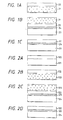
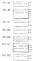
- a P-type Si monocrystalline substrate is provided, and all of it is made porous.
- epitaxial growth is effected on the substrate surface as made porous to form a thin film monocrystalline layer 22.
- the above P-type Si substrate is made porous by the anodization method by use of an HF solution.
- the porous Si layer 21 can be varied in its density to a range of 1.1 to 0.6 g/cm 3 by varying the HF solution concentration to 50 to 20% as compared with the density 2.33 g/cm 3 of the monocrystalline Si.
- the Si substrate 23 having the oxidized layer 24 on the surface is bonded onto the surface of the monocrystalline layer 22 on the porous Si substrate 21.
- the porous Si substrate 21 is all etched away to form a thin film-like monocrystalline silicon layer 22 remaining on the SiO 2 layer 24.
- the porous semiconductor layer is etched away without application of the oxidation treatment on the porous semiconductor layer, the oxidation swelling of the porous semiconductor layer can be prevented, whereby the influence of distortion on the monocrystalline layer as epitaxially grown can be prevented.
- the monocrystalline Si layer 22 equal to silicon wafer in crystallinity is formed flat and yet uniformly thinly over the whole wafer region with a large area on the oxidized Si layer 24 which is an insulating material.
- the semiconductor substrate thus obtained can be suitably used also with respect to preparation of an insulation separated electronic device.
- the thickness of the non-porous semiconductor crystalline layer to be formed on the porous semiconductor substrate may be desirably made preferably 50 ⁇ m or less, more preferably 20 ⁇ m or less, for forming a thin film semiconductor device on the above semiconductor monocrystalline layer.
- Bonding between the above non porous semiconductor monocrystal and the substrate having the insulating material surface should be preferably performed in an atmosphere of nitrogen, an inert gas or a gas mixture of these, or in an atmosphere containing an inert gas or nitrogen, and further desirably under heated state.
- etchants such as aqueous sodium hydroxide solution, aqueous potassium hydroxide solution, hydrofluoric acid-nitric acid-acetic acid mixed solution, etc.
- the substrate having an insulating material which can be used in the present invention may be one with at least its surface being constituted of an insulating material, or one with all of the substrate being constituted of an insulating material.
- the substrate with the surface being constituted of an insulating material may include monocrystalline or polycrystalline silicon substrates having the surface oxidized, electroconductive or semiconductive substrates having a layer of an insulating material such as oxide, nitride, boride, etc. formed on the surface, etc.
- Specific examples of the substrates wholly constituted of an insulating material may include substrates comprising insulating materials such as fused silica glass, sintered alumina, etc.
- a porous semiconductor substrate having a non-porous semiconductor monocrystalline layer may be also formed by applying a pore forming treatment on a substrate having a monocrystalline layer comprising a material which can be made porous with difficulty (e.g. N-type silicon) and a layer comprising a material which can be readily made porous (e.g. P-type silicon).
- a pore forming treatment on a substrate having a monocrystalline layer comprising a material which can be made porous with difficulty (e.g. N-type silicon) and a layer comprising a material which can be readily made porous (e.g. P-type silicon).
- the substrate may be also coated with an etching preventive material except for the porous semiconductor substrate during etching, so that the non-porous semiconductor monocrystalline layer and the substrate having the insulating material surface may not be deleteriously influenced by the etchant.
- the non-porous monocrystalline layer on the insulating material thus formed can be one having 5.0 x 10 -4 sec. or longer in terms of the life time of carriers, having remarkably less crystal defect such as through dislocation, etc. and also being extremely small in distribution of the layer thickness of the semiconductor monocrystalline layer.
- the dislocation defect density becomes 2 x 10 4 /cm 2 or less, and concerning the layer thickness of the semiconductor monocrystalline layer, within the range of the area of the semiconductor monocrystalline layer from 20 cm 2 to 500 cm 2 (5 cm (2 inches) wafer to 25 cm (10 inches) wafer), the difference between the maximum value and the minimum value of the thickness of the semiconductor monocrystalline layer can be suppressed below 10% or less based on the maximum value.
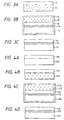
- Embodiment 2 is described in detail.
- a low impurity concentration layer 122 is formed by epitaxial growth according to various thin film growth methods.
- protons may be ion implanted into the surface of the P-type Si monocrystalline substrate 121 to form an N-type monocrystalline layer 122.
- the back surface of the P-type monocrystalline substrate 121 is denatured into a porous Si substrate 123 according to the anodization method by use of an HF solution.
- the porous Si layer 123 can be varied in its density to a range of 1.1 to 0.6 g/cm 3 by varying the HF solution concentration within the range of 50 to 20% as compared with the density of the monocrystalline Si of 2.33 g/cm 3 .
- the porous layer, as described above, is formed on the P-type substrate.
- the Si substrate 124 having the oxidized layer 125 on its surface is bonded to the surface of the monocrystalline Si layer 122 on the porous Si substrate 123.
- porous Si substrate 123 is all etched to leave a monocrystalline silicon layer 122 as thin film on the SiO 2 layer 125, thereby forming a semiconductor substrate.
- the monocrystalline Si layer 122 equal in crystallinity to silicon wafer is formed on the oxidized layer 125 which is an insulating material to be flat and to be yet made uniformly into thin layer, over the whole wafer region with a large area.
- the semiconductor substrate thus obtained can be used suitably also with respect to preparation or an insulation separated electronic device.
- Embodiment 2 is an example of the process of forming an N-type layer on a P-type substrate before pore formation, and then making selectively only the P-type substrate porous by anodization. Also in the present Embodiment, a semiconductor substrate having a semiconductor monocrystalline layer with the same performences as Embodiment 1 can be obtained.
- a P-type Si monocrystalline substrate is prepared and all of it is made porous. According to various growth methods, epitaxial growth is effected on the substrate surface made porous to form a thin film monocrystalline layer 12.
- the Si substrate having the oxidized layer 14 on the surface is bonded to the surface of the monocrystalline Si layer 12 on the porous Si substrate 11.
- an Si 3 N 4 layer 15 is deposited to cover over the whole of the bonded two silicon wafers as the anti-etching film.
- the Si 3 N 4 layer on the surface of the porous silicon substrate is removed.
- Apiezon Wax may be also employed in place of Si 3 N 4 .
- the porous Si substrate 11 is all etched and a monocrystalline silicon layer 12 made into a thin film remains on the SiO 2 layer 14 to form a semiconductor substrate.
- Fig. 3C shows a semiconductor substrate obtained in the present invention. More specifically, by removing the Si 3 N 4 layer 16 as the anti-etching film in Fig. 3B, a monocrystalline Si layer 12 of which crystallinity is equal to that of bulk wafer is formed through the SiO 2 layer 14 which is an insulating substance on the Si substrate 13, flat and yet uniformly into a thin layer, over the whole wafer region with a large area.
- the semiconductor substrate thus obtained can be used suitably also with respect to preparation of a discrete insulated electronic device. Also in the present Embodiment, a semiconductor substrate having a semiconductor monocrystalline layer with the same performances as Embodiment 1 can be obtained.
- a low impurity concentration layer 112 is formed by epitaxial growth according to various thin film growth methods.
- protons may be ion-implanted into the surface of the P-type Si monocrystalline substrate 111 to form an N-type monocrystalline layer 112.
- the back surface of the P-type monocrystalline substrate 111 is denatured into a porous Si substrate 113 according to the anodization method by use of an HF solution.
- the porous Si layer 113 can be varied in its density to a range of 1.1 to 0.6 g/cm 3 by varying the HF solution concentration to 50 to 20% as compared with the density of the monocrystalline Si of 2.33 g/cm 3 .
- the porous layer 113 as described above, is formed from the P-type substrate.
- the Si substrate 114 having the oxidized layer 115 on the surface is bonded on the surface of the monocrystalline Si layer 112 on the porous Si substrate 113.
- an Si 3 N 4 layer 116 is deposited to cover over the whole of the bonded two silicon wafers as the anti-etching film. Subsequently, as shown in Fig. 4C, the Si 3 N 4 layer on the surface of the porous silicon substrate is removed. As another anti-etching film 116, a material excellent in etching resistance such as Apiezon Wax may be also employed in place of Si 3 N 4 . Then, the porous Si substrate 113 is all etched to form a semiconductor substrate by retaining a monocrystalline silicon layer 112 made into a thin film on the SiO 2 layer 115. Fig. 4D shows a substrate having the semiconductor layer obtained in the present invention.
- a monocrystalline Si layer 112 is formed on the SiO 2 layer 115 which is the insulating material, flat and yet uniformly into a thin layer, over the whole wafer region with a large area.
- the semiconductor thus obtained will not be deleteriously affected by the etchant, and can be used suitably also with respect to preparation of a discrete insulated electronic device.
- the semiconductor substrate obtained in the present Embodiment has the same performances as that obtained in Embodiment 1.
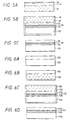
- a P-type Si monocrystalline substrate is prepared and all of it is made porous.
- a thin film monocrystalline layer 32 is formed by effecting epitaxial growth on the substrate surface made porous according to various growth methods.
- the Si substrate 33 having the oxidized layer 34 on the surface is bonded to the surface of the oxidized layer 36 formed on the monocrystalline Si layer 32 on the porous substrate 31.
- the bonding step is practiced by closely contacting the cleaned surfaces with each other, followed by heating in an inert gas atmosphere or nitrogen atmosphere.
- the oxidized layer 34 is formed in order to reduce the interface level of the non-porous monocrystalline layer 32 which is the final active layer.
- an Si 3 N 4 layer 35 is deposited as the anti-etching film to be coated on the bonded two silicon wafers as a whole. Subsequently, as shown in Fig.
- the Si 3 N 4 layer 35 on the surface of the porous silicon substrate 31 is removed.
- Apiezon Wax, etc. may be also employed in place of Si 3 N 4 .
- all of the porous Si substrate 31 is etched to have the monocrystalline silicon layer 32 made into a thin film remain on the SiO 2 layer, thereby forming a semiconductor substrate.
- Fig. 5C shows the substrate having the semiconductor layer obtained in the present invention. More specifically, by removing the Si 3 N 4 layer 35 as the anti-etching film shown in Fig 5B, the monocrystalline Si layer 32 equal in crystallinity to silicon wafer is formed through the SiO 2 layers 34 and 36 on the Si substrate 33, flat and yet uniformly into a thin layer, over the whole wafer region with a large area.
- the semiconductor substrate thus obtained can be used suitably also with respect to preparation of a discrete insulated electronic device. Also, the semiconductor substrate obtained in the present Embodiment has the same performances as that obtained in Embodiment 1.
- a low impurity concentration layer 132 is formed by epitaxial growth according to various thin film growth methods.
- the surface of the P-type Si monocrystalline substrate 131 is subjected to ion implantation of protons to form an N-type monocrystalline layer 132.
- the P-type Si monocrystalline substrate 131 is denatured from the back surface to a porous Si substrate 133 by the anodization method with an HF solution.
- the porous Si layer 133 can be varied in its density in the range of 1.1 to 0.6 g/cm 3 by varying the HF solution concentration to 50 to 20% as compared with the density of the monocrystalline Si of 2.33 g/cm 3 .
- the porous layer, as described above, is formed from the P-type substrate.
- the Si substrate 134 having the oxidized layer 135 is bonded onto the surface of the oxidized layer 137 formed on the monocrystalline Si layer 132 on the porous Si substrate 133.
- an Si 3 N 4 layer 136 is deposited to be coated on the bonded two silicon wafers as a whole. Then, as shown in Fig. 6D, the Si 3 N 4 layer 136 on the surface of the porous silicon substrate 133 is removed. Then the porous Si substrate 131 is all chemically etched to have a monocrystalline silicon layer made into a thin film remain on the SiO 2 layers 135 and 137, thereby forming a semiconductor substrate.
- the semiconductor substrate thus obtained is excellent in adhesion between the respective layers, and can be also used suitable also with respect to preparation of an isolation separated electronic device. Also, the semiconductor substrate obtained in the present Embodiment has the same performances as that obtained in Embodiment 1.
- a P-type Si monocrystalline substrate is prepared and all of it is made porous. According to various growth methods, epitaxial growth is effected on the substrate surface made porous to form a thin film monocrystalline layer 42.
- Fig. 7B by preparing another Si substrate 43 and after forming an oxidized layer 44 on its surface, the Si substrate 43 having the above oxidized layer 44 on the surface is bonded onto the surface of the oxidized layer 45 formed on the monocrystalline Si layer 42 on the porous Si substrate 41. This bonding step is practiced by closely contacting cleaned surfaces with each other, followed by heating in an inert gas atmosphere or nitrogen atmosphere.
- the oxidized layer 44 is formed in order to reduce the interface level of the monocrystalline layer 42 which is the active layer as the final semiconductor.
- the porous Si substrate 41 is all etched to have the monocrystalline silicon layer made into a thin film on the SiO 2 layers 44 and 45, thereby forming a semiconductor substrate.
- Fig. 7C shows the semiconductor substrate obtained in the present invention.
- a monocrystalline Si layer 42 equal in crystallinity to silicon wafer is formed through the SiO 2 layers 44 and 45 on the Si substrate 43, flat and yet uniformly into a thin layer, over the whole wafer region with a large area.
- the semiconductor substrate thus obtained can be also used suitably also as seen from the standpoint of preparation of an isolation separated electron device. Also, the semiconductor substrate obtained in the present embodiment has the same performances as that obtained in Embodiment 1.
- a low impurity concentration layer 142 is formed by epitaxial growth according to various thin film growth methods.
- the surface of the P-type Si monocrystalline substrate 141 is subjected to ion implantation of protons to form an N-type monocrystalline layer 142.
- the P-type Si monocrystalline substrate 141 is denatured from the back surface to a porous Si substrate 143 by the anodization method with an HF solution.
- the porous Si layer 143 can be varied in its density in the range of 1.1 to 0.6 g/cm 3 by varying the HP solution concentration to 50 to 20% as compared with the density of the monocrystalline Si of 2.33 g/cm 3 .
- the porous layer, as described above, is formed on the P-type substrate 141.
- the Si substrate 144 having the oxidized layer 145 is bonded onto the surface of the oxidized layer 146 formed on the monocrystalline Si layer 142 on the porous Si substrate 143.
- porous Si substrate is all chemically etched to have a monocrystalline silicon layer made into a thin film remain on the SiO 2 layers 145 and 146, thereby forming a semiconductor substrate.
- Fig. 8D shows the semiconductor substrate obtained in the present invention.
- a monocrystalline Si layer 142 equal in crystallinity to silicon wafer is formed through the SiO 2 layers 145 and 146 on the Si substrate 144, flat and yet uniformly into a thin layer, over the whole wafer region with a large area.
- the semiconductor substrate thus obtained can be also used suitably also with respect to preparation of an isolation separated electronic device. Also, the semiconductor substrate obtained in the present Embodiment has the same performances as that obtained in Embodiment 1.
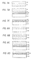
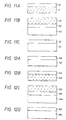
- a P-type Si monocrystalline substrate is prepared, and all of it is made porous. According to various growth methods, epitaxial growth is effected on the surface of the substrate 51 made porous to form a thin film monocrystalline layer 52.
- a light-transmissive substrate 53 represented by glass is prepared and the light-transmissive substrate 53 is bonded onto the surface of the monocrystalline Si layer 52 on the porous Si substrate 51.
- Fig. 9B shows the anti-etching film 54.
- an Si 3 N 4 layer 54 is deposited to be coasted on the bonded two substrates as a whole.
- Fig. 9C shows the Si 3 N 4 layer 54 on the surface of the porous silicon substrate.
- the porous Si substrate 51 is all etched away to have a monocrystalline silicon layer 52 made into a thin film remain on the light-transmissive substrate 53, thereby forming a semiconducor substrate.
- Fig. 9C shows the semiconductor substrate obtained in the present invention.
- the semiconductor substrate thus obtained can be also used suitable also as seen from the standpoint of preparation of an electronic device isolation separated with a light-transmissive insulating material. Also, the semiconductor obtained in the present Embodiment has the same performances as that obtained in Embodiment 1.
- a low impurity concentration layer 152 is formed by epitaxial growth according to various thin film growth methods.
- the surface of the P-type Si monocrystalline substrate 151 is subjected to ion implantation of protons to form an N-type monocrystalline layer 152.
- the P-type Si monocrystalline substrate 151 is denatured from the back surface to a porous Si substrate 153 by the anodization method with an HF solution.
- the porous Si layer 163 can be varied in its density in the range of 1.1 to 0.6 g/cm 3 by varying the HF solution concentration to 50 to 20% as compared with the density of the monocrystalline Si of 2.33 g/cm 3 .
- the porous layer 153 as described above, is formed on the P-type substrate 151.
- a light-transmissive substrate 154 onto the surface of the monocrystalline Si layer 152 on the porous Si substrate 153 is bonded the light-transmissive substrate 154. Then, as shown in Fig. 10C, as an anti-etching film 155, an Si 3 N 4 layer, etc. is deposited to be coated on the bonded two substrates as a whole. Subsequently, as shown in Fig. 10D, the Si 3 N 4 layer 155 on the surface of the porous silicon substrate 153 is removed. Then, the porous Si substrate 153 is all etched away to have the monocrystalline silicon layer 152 made into a thin film remain on the light-transmissive substrate 154, thereby forming a semiconductor substrate.
- Fig. 10D shows the semiconductor substrate obtained in the present invention. It is the monocrystalline Si layer 152 equal in crystallinity to silicon wafer formed on the light-transmissive substrate 154, flat and yet uniformly into a thin layer, over the whole wafer region with a large area.
- the semiconductor substrate thus obtained can be also used suitably also with respect to preparation of an isolation separated electronic device with a light-transmissive insulating material. Also, the semiconductor substrate obtained in the present Embodiment has the same performances as that obtained in Embodiment 1.
- a P-type Si monocrystalline substrate is prepared, and all of it is made porous. According to various growth methods, epitaxial growth is effected on the surface of the substrate 61 made porous to form a thin film monocrystalline layer 62.
- a light-transmissive substrate 63 represented by glass is prepared and the light-transmissive substrate 63 is bonded to the surface of the monocrystalline Si layer 62 on the porous Si substrate 61.
- porous Si substrate 61 is all etched to have the monocrystalline silicon layer 62 made into a thin film remain on the light-transmissive substrate 63, thereby forming a semiconductor substrate.
- Fig. 11C shows the semiconductor substrate obtained in the present invention. It is the monocrystalline Si layer 62 equal in crystallinity to silicon wafer formed on the light-transmissive substrate 63, flat and yet uniformly into a thin layer, over the whole wafer region with a large area.
- the semiconductor thus obtained can be also suitably used also with respect to preparation of an electronic device isolation separated with a light-transmissive insulating material.
- a low impurity concentration layer 162 is formed by epitaxial growth according to various thin film growth methods.
- the surface of the P-type Si monocrystalline substrate 161 is subjected to ion implantation of protons to form an N-type monocrystalline layer 162.
- the P-type Si monocrystalline substrate 161 is denatured from the back surface to a porous Si substrate 163 by the anodization method with an HF solution.
- the porous Si layer 163 can be varied in its density in the range of 1.1 to 0.6 g/cm 3 by varying the HF solution concentration to 50 to 20% as compared with the density of the monocrystalline Si of 2.33 g/cm 3 .
- the porous layer 163, as described above, is formed on the P-type substrate 163.
- the porous Si substrate 163 is all etched away to have the monocrystalline silicon layer 162 made into a thin film remain on the light-transmissive substrate 164, thereby forming a semiconductor substrate.
- Fig. 12D shows the semiconductor substrate obtained in the present invention. It is the monocrystalline Si layer 162 equal in crystallinity to silicon wafer formed on the light-transmissive substrate 164, flat and yet uniformly into a thin layer, over the whole wafer region with a large area.
- the semiconductor substrate thus obtained can be also used suitably also with respect to preparation of an isolation separated electronic device with a light-transmissive insulating material. Also, the semiconductor substrate obtained in the present Embodiment has the same performances as that obtained in Embodiment 1.
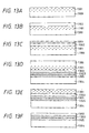
- Figs. 13A to 13F This Embodiment is described by referring to Figs. 13A to 13F.
- a porous region 1301 is formed on a part of an Si monocrystalline substrate 1300.
- a thin film Si monocrystalline layer 1302 is formed according to various crystal growth methods on the porous region 1301 (Fig. 13B).
- an oxidized film 1303 Fig. 13C.
- the oxidized film 1305 formed on the surface of another Si substrate 1304 is bonded to the above oxidized film 1303 (Fig. 13D).
- the Si monocrystalline substrate 1300 remaining without being made porous is removed by mechanical polishing or etching to have the porous region 1301 exposed (Fig. 13E).
- the porous region 1301 is etched away to form a semiconductor substrate having a thin film Si monocrystalline layer on an insulating material (Fig. 13F).
- the time required for making the substrate porous can be shortened and also the time for etching away the porous Si substrate can be shortened, whereby substrate formation can be effected highly efficiently.
- the thin film Si monocrystalline layer 1302 directly to the oxidized film 1305 without forming the oxidized film 1303 shown in Fig. 13, and it is also possible to bond an insulating substrate such as glass, etc. in place of the oxidized film 1305 formed on the Si substrate 1304.
- the semiconductor substrate thus obtained has the same excellent performances as those of the semiconductor substrate obtained in Embodiments 1 to 12.
- a P-type (100) monocrystalline Si substrate (Si wafer) having a diameter of 7.6 cm (3 inches) and a thickness of 200 microns was anodized in a 50% HF solution.
- the current density at this time was 100 mA/cm 2 .
- the porous structure formation rate at this time was 8.4 ⁇ m/min. and the P-type (100) Si substrate having a thickness of 200 microns as a whole was made porous in 24 minutes.
- chemical etching rate of ordinary Si monocrystal relative to hydrofluoric acid-nitric acid-acetic acid solution is about a little lower than 1 micron per minute (hydrofluoric acid-nitric acid-acetic acid solution, 1:3:8), but the chemical etching rate of a porous layer is accelerated by about 100-fold thereof. That is, the Si substrate 21 made porous having a thickness of 200 microns was removed in 2 minutes.
- a monocrystalline Si layer 22 having a thickness of 0.5 ⁇ m could be formed on the SiO 2 layer 24.
- the thickness of the monocrystalline Si layer obtained was examined by use of Scanning Ellipsometer. Specifically, the whole surface of the 3 inches wafer was scanned for the measurement. As the result, within the plane of the 3 inches wafer, the difference between the maximum value and the minimum value of the thickness of the monocrystalline Si layer was found to be suppressed 5% or less relative to the maximum value of the thickness. As the result of plan view observation of the monocrystalline Si layer by transmission electron microscopy, the dislocation defect density was found to be suppressed 1 x 10 3 /cm 2 or less, whereby it could be confirmed that no new crystal defect had been introduced in the monocrystalline Si layer formation step to maintain good crystallinity. When the life time of minority carriers was measured for the monocrystalline Si layer by use of the MOS C-t method, a high value of 2.0 x 10 -3 sec. was exhibited.
- a P-type (100) monocrystalline Si substrate having a diameter of 4 inches and a thickness of 500 microns was anodized in a 50% HF solution.
- the current density at this time was 100 mA/cm 2 .
- the porous structure formation rate at this time was 8.4 ⁇ m/min, and the P-type (100) Si substrate having a thickness of 500 microns as a whole was made porous in 60 minutes.
- Si epitaxial layer 22 On the P-type (100) porous Si substrate 21 was grown at low temperature an Si epitaxial layer 22 to a thickness of 0.5 microns by the plasma CVD method.
- the deposition conditions are as follows:
- the porous Si substrate 21 was chemically etched away by use of hydrofluoric acid-nitric acid-acetic acid solution (1:3:8).
- chemical etching rate of ordinary Si monocrystal relative to hydrofluoric acid-nitric acid-acetic acid solution is about a little lower than 1 micron per minute (hydrofluoric acid-nitric acid-acetic acid solution, 1:3:8), but the chemical etching rate of a porous layer is accelerated by about 100-fold thereof. That is, the Si substrate 21 made porous having a thickness of 500 microns was removed in 5 minutes.
- a monocrystalline Si layer having a thickness of 0.5 ⁇ m could be formed on the SiO 2 layer 24.
- the thickness of the monocrystalline Si layer obtained was examined by use of Scanning Ellipsometer. Specifically, the whole surface of the 4 inches wafer was scanned for the measurement. As the result, within the plane of the 4 inches wafer, the difference between the maximum value and the minimum value of the thickness of the monocrystalline Si layer was found to be suppressed 7% or less relative to the maximum value of the thickness. As the result of plan view observation of the monocrystalline Si layer by transmission electron microscopy, the dislocation defect density was found to be suppressed 1 x 10 3 /cm 2 or less, whereby it could be confirmed that no new crystal defect had been introduced in the monocrystalline Si layer formation step to maintain good crystallinity. When the life time of minority carriers was messured for the monocrystalline Si layer by use of the MOS C-t method, a high value of 2.0 x 10 -3 sec. was exhibited.
- a P-type (100) monocrystalline Si substrate (Si water) having a diameter of 3 inches and a thickness of 200 microns was anodized in a 50% HF solution.
- the current density at this time was 100 mA/cm 2 .
- the porous structure formation rate at this time was 8.4 ⁇ m/min. and the P-type (100) Si substrate having a thickness of 200 microns as a whole was made porous in 24 minutes.
- the deposition conditions are as follows:
- Substrate direct current bias 5 V.
- the porous Si substrate 21 was chemically etched away by use of hydrofluoric acid-nitric acid-acetic acid solution (1:3:8).
- chemical etching rate or ordinary Si monocrystal to hydrofluoric acid-nitric acid-acetic acid solution is about a little lower than 1 micron per minute (hydrofluoric acid-nitric acid-acetic acid solution, 1:3:8), the chemical etching rate or a porous layer is accelerated by about 100-fold thereof. That is, the Si substrate 21 made porous having a thickness of 200 microns was removed in 2 minutes.
- a monocrystalline Si layer having a thickness of 0.5 ⁇ m could be formed on the SiO 2 layer 24.
- a P-type (100) monocrystalline Si substrate having a diameter of 3 inches and a thickness of 200 microns was anodized in a 50% HF solution.
- the current density at this time was 100 mA/cm 2 .
- the porous structure formation rate at this time was 8.4 ⁇ m/min, and the P-type (100) Si substrate having a thickness of 200 microns as a whole was made porous in 24 minutes.
- Si epitaxial layer 22 On the P-type (100) porous Si substrate 21 was grown an Si epitaxial layer 22 to a thickness of 0.5 microns by the liquid phase growth method.
- the growth conditions are as follows:
- the Si substrate 21 was chemically etched away by use of hydrofluoric acid-nitric acid-acetic acid solution (1:3:8). As the result, the Si substrate 21 made porous having a thickness of 200 microns was removed in 2 minutes.
- a monocrystalline Si layer 22 having a thickness of 0.5 ⁇ m could be formed on the SiO 2 layer 24.
- a P-type (100) monocrystalline Si substrate having a diameter of 3 inches and a thickness of 200 microns was anodized in a 50% HF solution.
- the current density at this time was 100 mA/cm 2 .
- the porous structure formation rate at this time was 8.4 ⁇ m/min, and the P-type (100) Si substrate having a thickness of 200 microns as a whole was made porous in 24 minutes.
- the deposition conditions are as follows:
- the Si substrate 21 was chemically etched away by use of hydrofluoric acid-nitric acid-acetic acid solution (1:3:8). As the result, the Si substrate 21 made porous having a thickness of 200 microns was removed in 2 minutes.
- a monocrystalline Si layer having a thickness of 0.5 ⁇ m could be formed on the SiO 2 layer 24.
- SiH 2 Cl 2 was employed as the source gas, although it was necessary to elevate the growth temperture by some ten degrees, the accelerted etching characteristics inherent in the porous substrate were maintained.
- Si epitaxial layer 122 On a P-type (100) Si substrate 121 having a diameter of 3 inches and a thickness of 200 microns was grown an Si epitaxial layer 122 with a thickness of 1 micron by the CVD method.
- the deposition conditions are as follows:
- the substrate 121 was anodized in a 50% HF solution.
- the current density at this time was 100 mA/cm 2 .
- the porous structure formation rate at this time was 8.4 ⁇ m/min. and the P-type (100) Si substrate 121 having a thickness of 200 microns as a whole was made porous in 24 minutes. In this anodization, only the P-type (100) Si substrate 121 was made porous, and there was no change in the Si epitaxial layer 122.
- the epitaxial layer 122 was superposed another Si substrate 124 with an oxidized layer 125 of 5000 angstroms formed on the surface, and by heating in a nitrogen atmosphere at 800 °C for 0.5 hour, the two Si substrates were bonded firmly together. Then, the porous Si substrate 123 was chemically etched away by use of hydrofluoric acid-nitric acid-acetic acid solution (1:3:8). As the result, the Si substrate 123 made porous having a thickness of 200 microns was removed in 2 minutes.
- the thickness of the monocrystalline Si layer obtained was examined by use of Scanning Ellipsometer. As the result, within the plane of the 3 inches wafer, the difference between the maximum value and the minimum value of the thickness of the monocrystalline Si layer was found to be suppressed 5% or less relative to the maximum value of the thickness. As the result of plan view observation of the monocrystalline Si layer by a transmission electron microscopy, the dislocation defect density was found to be suppressed 1 x 10 3 /cm 2 or less, whereby it could be confirmed that no new crystal defect had been introduced in the monocrystalline Si layer formation step to maintain good crystallinity. When the life time of minority carriers was measured for the monocrystalline Si layer by use of the microwave reflection method, a high value of 2.0 x 10 -3 sec. was exhibited.
- Si epitaxial layer 122 On a P-type (100) Si substrate having a diameter of 3 inches and a thickness of 200 microns was grown an Si epitaxial layer 122 to a thickness of 0.5 micron by the CVD method.
- the deposition conditions are as follows:
- the substrate was anodized in a 50% HF solution.
- the current density at this time was 100 mA/cm 2 .
- the porous structure formation rate at this time was 8.4 ⁇ m/min. and the P-type (100) Si substrate 121 having a thickness of 200 microns as a whole was made porous in 24 minutes. In this anodization, only the P-type (100) Si substrate was made porous, and there was no change in the Si epitaxial layer 122.
- the epitaxial layer 122 was superposed another Si substrate 124 with an oxidized layer 125 of 5000 angstroms formed on the surface, and by heating in a nitrogen atmosphere at 800 °C for 0.5 hour, the two Si substrates were bonded firmly together. Then, the porous Si substrate 123 was chemically etched away by use of hydrofluoric acid-nitric acid-acetic acid solution (1:3:8). As the result, the Si substrate 123 made porous having a thickness of 200 microns was removed in 2 minutes.
- a P-type (100) Si substrate 121 having a diameter of 3 inches and a thickness of 200 microns was formed an N-type Si layer 122 to a thickness of 1 micron by ion implantation of protons into the surface.
- the amount of H + implanted was found to be 5 x 10 15 (ions/cm 2 ).
- the substrate 121 was anodized in a 50% HF solution.
- the current density at this time was 100 mA/cm 2 .
- the porous structure formation rate at this time was 8.4 ⁇ m/min, and the P-type (100) Si substrate 121 having a thickness of 200 microns as a whole was made porous in 24 minutes.
- the P-type (100) Si substrate 121 was made porous, and there was no change in the N-type Si layer 122.
- the N-type Si layer 122 was superposed another Si substrate 124 with an oxidized layer 125 of 5000 angstroms formed on the surface, and by heating in a nitrogen atmosphere at 800 °C for 0.5 hour, the two Si substrates were bonded firmly together.
- the porous Si substrate 123 was chemically etched away by use of hydrofluoric acid-nitric acid-acetic acid solution (1:3:8). As the result, the Si substrate 123 made porous having a thickness of 200 microns was removed in 2 minutes.
- a P-type (100) monocrystalline Si substrate having a diameter of 3 inches and a thickness of 200 microns was anodized in a 50% HF solution.
- the current density at this time was 100 mA/cm 2 .
- the porous structure formation rate at this time was 8.4 ⁇ m/min, and the P-type (100) Si substrate having a thickness of 200 microns as a whole was made porous in 24 minutes.
- Si epitaxial layer 12 On the P-type (100) porous Si substrate 11 was grown an Si epitaxial layer 12 to a thickness of 0.5 microns by the MBE (Molecular Beam Epitaxy) method.
- MBE Molecular Beam Epitaxy
- the epitaxial layer 12 was superposed another Si substrate 13 with an oxidized layer 14 of 5000 angstroms formed on the surface, and by heating in a nitrogen atmosphere at 800 °C for 0.5 hour, the two Si substrates were bonded firmly together.
- Si 3 N 4 was coated on the bonded substrate by the low pressure CVD method to a thickness of 0.1 ⁇ m. Thereafter, only the silicon nitride film on the porous substrate was removed by reactive ion etching. Then, the porous Si substrate 11 was chemically etched away by use of hydrofluoric acid-nitric acid-acetic acid solution (1:3:8).
- the Si substrate 11 made porous having a thickness of 200 microns was removed in 2 minutes. After removal of the Si 3 N 4 layer 15, a substrate having a monocrystalline Si layer having a thickness of 0.5 ⁇ m on the SiO 2 layer 14 could be formed.
- a P-type (100) monocrystalline Si substrate having a diameter of 3 inches and a thickness of 200 microns was anodized in a 50% HF solution.
- the current density at this time was 100 mA/cm 2 .
- the porous structure formation rate at this time was 8.4 ⁇ m/min, and the P-type (100) Si substrate having a thickness of 200 microns as a whole was made porous in 24 minutes.
- Si epitaxial layer 12 On the P-type (100) porous Si substrate 11 was grown an Si epitaxial layer 12 to a thickness of 0.5 microns by the plasma CVD method.
- the deposition conditions are as follows:
- the epitaxial layer 12 was superposed another Si substrate with an oxidized layer 14 of 5000 angstroms formed on the surface, and by heating in a nitrogen atmosphere at 800 °C for 0.5 hour, the two Si substrates were bonded firmly together.
- Si 3 N 4 was coated on the bonded substrate by the low pressure CVD method to a thickness of 0.1 ⁇ m. Thereafter, only the silicon nitride film on the porous substrate 11 was removed by reactive ion etching. Then, the porous Si substrate 11 was chemically etched away by use of hydrofluoric acid-nitric acid acetic acid solution (1:3:8).
- the Si substrate 11 made porous having a thickness of 200 microns was removed in 2 minutes. After removal of the Si 3 N 4 layer 15, a substrate having a monocrystalline Si layer 12 having a thickness of 0.5 ⁇ m on the SiO 2 layer could be formed.
- the thickness of the monocrystalline Si layer obtained was examined by use of Scanning Ellipsometer. As the result, within the plane of the 3 inches wafer, the difference between the maximum value and the minimum value of the thickness of the monocrystalline Si layer was found to be suppressed 5% or less relative to the maximum value of the thickness. As the result of observation by defect delineation etching by use of Sirtle etching, the dislocation defect density was found to be suppressed 1 x 10 3 /cm 2 or less, whereby it could be confirmed that no new crystal defect had been introduced in the monocrystalline Si layer formation step to maintain good crystallinity. When the life time of minority carriers was measured for the monocrystalline Si layer by use of the MOS C-t method, a high value of 2.0 x 10 -3 sec. was exhibited.
- a P-type (100) monocrystalline Si substrate having a diameter of 3 inches and a thickness of 200 microns was anodized in a 50% HF solution.
- the current density at this time was 100 mA/cm 2 .
- the porous structure formation rate at this time was 8.4 ⁇ m/min. and the P-type (100) Si substrate having a thickness of 200 microns as a whole was made porous in 24 minutes.
- the deposition conditions are as follows:
- the epitaxial layer 12 was superposed another Si substrate with an oxidized layer 14 of 5000 angstroms formed on the surface, and by heating in a nitrogen atmosphere at 800 °C for 0.5 hour, the two Si substrates were bonded firmly together.
- Si 3 N 4 was coated on the bonded substrate by the low pressure CVD method to a thickness of 0.1 ⁇ m. Thereafter, only the silicon nitride film on the porous substrate was removed by reactive ion etching. Then, the porous Si substrate 11 was chemically etched away by use of hydrofluoric acid-nitric acid-acetic acid solution (1:3:8).
- the Si substrate 11 made porous having a thickness of 200 microns was removed in 2 minutes. After removal of the Si 3 N 4 layer 15, a substrate having a monocrystalline Si layer 12 having a thickness of 0.5 ⁇ m on the SiO 2 layer 14 could be formed.
- a P-type (100) monocrystalline Si substrate having a diameter of 3 inches and a thickness of 200 microns was anodized in a 50% HF solution.
- the current density at this time was 100 mA/cm 2 .
- the porous structure formation rate at this time was 8.4 ⁇ m/min, and the P-type (100) 51 substrate having a thickness of 200 microns as a whole was made porous in 24 minutes.
- the growth conditions are as follows:
- the epitaxial layer 12 was superposed another Si substrate 13 with an oxidized layer 14 of 5000 angstroms formed on the surface, and by heating in a nitrogen atmosphere at 800 °C for 0.5 hour, the two Si substrates were bonded firmly together.
- Si 3 N 4 was coated on the bonded substrate by the low pressure CVD method to a thickness of 0.1 ⁇ m. Thereafter, only the silicon nitride film on the porous substrate was removed by reactive ion etching. Then, the porous Si substrate 11 was chemically etched away by use of hydrofluoric acid-nitric acid-acetic acid solution (1:3:8).
- the Si substrate 11 made porous having a thickness of 200 microns was removed in 2 minutes. After removal of the Si 3 N 4 layer 15, a substrate having a monocrystalline Si layer 12 having a thickness of 0.5 ⁇ m on the SiO 2 layer 14 could be formed.
- a P-type (100) monocrystalline Si substrate having a diameter of 3 inches and a thickness of 200 microns was anodized in a 50% HF solution.
- the current density at this time was 100 mA/cm 2 .
- the porous structure formation rate at this time was 8.4 ⁇ m/min. and the P-type (100) Si substrate having a thickness of 200 microns as a whole was made porous in 24 minutes.
- the deposition conditions are as follows:
- the epitaxial layer 12 was superposed another Si substrate 13 with an oxidized layer 14 of 5000 angstroms formed on the surface, and by heating in a nitrogen atmosphere at 800 °C for 0.5 hour, the two Si substrates were bonded flrmly together.
- Si 3 N 4 was coated on the bonded substrate by the low pressure CVD method to a thickness of 0.1 ⁇ m. Thereafter, only the silicon nitride film 15 on the porous substrate 11 was removed by reactive ion etching. Then, the porous Si substrate 11 was chemically etched away by use of hydrofluoric acid-nitric acid-acetic acid solution (1:3:8).
- the Si substrate 11 made porous having a thickness of 200 microns was removed in 2 minutes. After removal of the Si 3 N 4 layer 15, a substrate having a monocrystalline Si layer having a thickness of 0.5 ⁇ m on the SiO 2 layer 14 could be formed.
- Si epitaxial layer 112 On a P-type (100) Si substrate 111 having a diameter of 3 inches and a thickness of 200 microns was grown an Si epitaxial layer 112 with a thickness of 1 micron by the CVD method.
- the deposition conditions are as follows:
- the substrate was anodized in a 50% HF solution.
- the current density at this time was 100 mA/cm 2 .
- the porous structure formation rate at this time was 8.4 ⁇ m/min, and the P-type (100) Si substrate 111 having a thickness of 200 microns as a whole was made porous in 24 minutes.
- the P-type (100) Si substrate 111 was made porous, and there was no change in the Si epitaxial layer 112.
- Si 3 N 4 was coated on the bonded substrate by the low pressure CVD method to a thickness of 0.1 ⁇ m. Thereafter, only the nitride film on the porous substrate was removed by reactive ion etching. Then, the porous Si substrate 111 was chemically etched away by use of hydrofluoric acid-nitric acid-acetic acid solution (1:3:8). As the result, the Si substrate 113 made porous having a thickness of 200 microns was removed in 2 minutes. After removal of the Si 3 N 4 layer 116, a substrate having a monocrystalline Si layer 112 having a thickness of 1 ⁇ m could be formed on SiO 2 .
- the thickness of the monocrystalline Si layer obtained was examined by use of Scanning Ellipsometer. As the result, within the plane of the 3 inches wafer, the difference between the maximum value and the minimum value of the thickness of the monocrystalline Si layer was found to be suppressed 5% or less relative to the maximum value of the thickness. As the result of plan view observation of the monocrystalline Si layer by transmission electron microscopy, the dislocation defect density was found to be suppressed 1 x 10 3 /cm 2 or less, whereby it could be confirmed that no new crystal defect had been introduced in the monocrystalline Si layer formation process to maintain good crystallinity. When the life time of minority carriers was measured for the monocrystalline Si layer by use of the microwave reflection method, a high value of 2.0 x 10 -3 sec. was exhibited.
- Si epitaxial layer 112 On a P-type (100) Si substrate 111 having a diameter of 3 inches and a thickness of 200 microns was grown an Si epitaxial layer 112 to a thickness of 0.5 micron by the CVD method.
- the deposition conditions are as follows:
- the substrate was anodized in a 50% HF solution.
- the current density at this time was 100 mA/cm 2 .
- the porous structure formation rate at this time was 8.4 ⁇ m/min. and the P-type (100) Si substrate 111 having a thickness of 200 microns as a whole was made porous in 24 minutes. In this anodization, only the P-type (100) Si substrate 111 was made porous, and there was no change in the Si epitaxial layer 112.
- an Si substrate 114 with an oxidized layer of 5000 angstroms formed on the surface, and by heating in a nitrogen atmosphere at 800 °C for 0.5 hour, the two Si substrates were bonded firmly together.
- Si 3 N 4 was coated on the bonded substrate by the low pressure CVD method to a thickness of 0.1 ⁇ m. Thereafter, only the silicon nitride film 116 on the porous substrate 113 was removed by reactive ion etching. Then, the porous Si substrate 113 was chemically etched away by use of hydrofluoric acid-nitric acid-acetic acid solution (1:3:8).
- the Si substrate 113 made porous having a thickness of 200 microns was removed in 2 minutes.
- a substrate having a monocrystalline Si layer 112 having a thickness of 0.5 ⁇ m could be formed on the SiO 2 layer 115.
- a P-type (100) Si substrate 111 having a diameter of 3 inches and a thickness of 200 microns was formed an N-type Si layer 112 to a thickness of 1 micron by ion implantation of protons into the surface.
- the amount of H + implanted was found to be 5 x 10 15 (ions/cm 2 ).
- the substrate was anodized in a 50% HF solution.
- the current density at this time was 100 mA/cm 2 .
- the porous structure formation rate at this time was 8.4 ⁇ m/min. and the P-type (100) Si substrate 111 having a thickness of 200 microns as a whole was made porous in 24 minutes.
- the porous Si substrate 113 was chemically etched away by use of hydrofluoric acid-nitric acid-acetic acid solution (1:3:8). As the result, the Si substrate 113 made porous having a thickness of 200 microns was removed in 2 minutes. After removal of the Si 3 N 4 layer 116, a substrate having a monocrystalline Si layer 112 having a thickness of 1.0 ⁇ m could be formed on the SiO 2 . As the result of cross-sectional observation by transmission electron microscopy, it could be confirmed that no new crystal defect had been introduced in the Si layer to maintain good crystallinity.
- a P-type (100) monocrystalline Si substrate having a diameter of 3 inches and a thickness of 200 microns was anodized in a 50% HF solution.
- the current density at this time was 100 mA/cm 2 .
- the porous structure formation rate at this time was 8.4 ⁇ m/min. and the P-type (100) Si substrate having a thickness of 200 microns as a whole was made porous in 24 minutes.
- Si epitaxial layer 32 On the P-type (100) porous Si substrate 31 was grown an Si epitaxial layer 32 to a thickness of 0.5 microns by the MBE (Molecular Beam Epitaxy) method.
- MBE Molecular Beam Epitaxy
- an oxide layer 36 with a thickness of 1000 angstroms was formed on the surface of the epitaxial layer 32 .
- Si 3 N 4 was coated on the bonded substrate by the low pressure CVD method to a thickness of 0.1 ⁇ m. Thereafter, only the silicon nitride film on the porous substrate was removed by reactive ion etching. Then, the porous Si substrate 31 was chemically etched away by use of hydrofluoric acid-nitric acid-acetic acid solution (1:3:8).
- the Si substrate 31 made porous having a thickness of 200 microns was removed in 2 minutes.
- a substrate having a thin film monocrystalline Si layer 32 could be formed on the SiO 2 .
- a P-type (100) monocrystalline Si substrate having a diameter of 3 inches and a thickness of 200 microns was anodized in a 50% HF solution.
- the current density at this time was 100 mA/cm 2 .
- the porous structure formation rate at this time was 8.4 ⁇ m/min, and the P-type (100) Si substrate having a thickness of 200 microns as a whole was made porous in 24 minutes.
- the deposition conditions are as follows:
- an oxide layer 36 with a thickness of 1000 angstroms was formed on the surface of the epitaxial layer 32 .
- Si substrate 33 having an oxide layer 34 of 5000 angstroms formed on the surrace was superposed the above oxide layer 36, and by heating in a nitrogen atmosphere at 800 °C for 0.5 hour, the both were bonded firmly together.
- Si 3 N 4 was coated on the bonded substrate by the low pressure CVD method to a thickness of 0.1 ⁇ m. Thereafter, only the silicon nitride film on the porous substrate was removed by reactive ion etching. Then, the porous Si substrate 31 was chemically etched away by use of a KOH solution (6 M). As the result, the Si substrate 31 made porous having a thickness of 200 microns was removed in 2 minutes. After removal of the Si 3 N 4 layer, a substrate having a monocrystalline Si layer 32 with good crystallinity could be formed on the SiO 2 layer.
- the thickness of the monocrystalline Si layer obtained was examined by use of Scanning Ellipsometer. As the result, within the plane of the 3 inches wafer, the difference between the maximum value and the minimum value of the thickness of the monocrystalline Si layer was found to be suppressed 5% or less relative to the maximum value of the thickness. As the result of plan view observation of the monocrystalline Si layer by transmission electron microscopy, the dislocation defect density was found to be suppressed 1 x 10 3 /cm 2 or less, whereby it could be confirmed that no new crystal defect had been introduced in the monocrystalline Si layer formation process to maintain good crystallinity. When the life time of minority carriers was measured for the monocrystalline Si layer by use of the MOS C-t method, a high value of 2.0 x 10 -3 sec. was exhibited.
- a P-type (100) monocrystalline Si substrate having a diameter of 3 inches and a thickness of 200 microns was anodized in a 50% HF solution.
- the current density at this time was 100 mA/cm 2 .
- the porous structure formation rate at this time was 8.4 ⁇ m/min. and the P-type (100) Si substrate having a thickness of 200 microns as a whole was made porous in 24 minutes.
- the deposition conditions are as follows:
- an oxide layer 36 with a thickness of 1000 angstroms was formed on the surface of the epitaxial layer 32 .
- Si substrate 33 having an oxide layer 34 of 5000 angstroms formed on the surface was superposed the above oxide layer 36, and by heating in a nitrogen atmosphere at 800 °C for 0.5 hour, the both were bonded firmly together.
- Si 3 N 4 was coated on the bonded substrate by the low pressure CVD method to a thickness of 0.1 ⁇ m. Thereafter, only the nitride film on the porous substrate 31 was removed by reactive ion etching. Then, the porous Si substrate 31 was chemically etched away by use of a hydrofluoric acid-nitric acid-acetic acid solution (1:3:8). As the result, the Si substrate 31 made porous having a thickness of 200 microns was removed in 2 minutes. After removal of the Si 3 N 4 layer, a substrate having a monocrystalline Si layer 32 with good crystallinity could be formed on the SiO 2 layer.
- a P-type (100) monocrystalline Si substrate having a diameter of 3 inches and a thickness of 200 microns was anodized in a 50% HF solution.
- the current density at this time was 100 mA/cm 2 .
- the porous structure formation rate at this time was 8.4 ⁇ m/min. and the P-type (100) Si substrate having a thickness of 200 microns as a whole was made porous in 24 minutes.
- the growth conditions are as follows:
- an oxide layer 36 with a thickness of 1000 angstroms was formed on the surface of the epitaxial layer 32 .
- Si substrate 33 having an oxide layer 34 of 5000 angstroms formed on the surface was superposed the above oxide layer 36, and by heating in a nitrogen atmosphere at 700 °C for 0.5 hour, the both were bonded firmly together.
- Si 3 N 4 was coated on the bonded substrate by the low pressure CVD method to a thickness of 0.1 ⁇ m. Thereafter, only the silicon nitride film on the porous substrate was removed by reactive ion etching. Then, the porous Si substrate 31 was chemically etched away by use of a hydrofluoric acid-nitric acid-acetic acid solution (1:3:8).
- the Si substrate 31 made porous having a thickness of 200 microns was removed in 2 minutes. After removal of the Si 3 N 4 layer 35, a substrate having a monocrystalline Si layer 32 could be formed on the SiO 2 . The same effect was obtained also when Apiezon Wax was coated in place of the Si 3 N 4 layer, whereby only the Si substrate made porous could be completely removed.
- the thickness of the monocrystalline Si layer obtained was examined by use of Scanning Ellipsometer. As the result, within the plane of the 3 inches wafer, the difference between the maximum value and the minimum value of the thickness of the monocrystalline Si layer was found to be suppressed 5% or less relative to the maximum value of the thickness. As the result of plan view observation of the monocrystalline Si layer by transmission electron microscopy, the dislocation defect density was found to be suppressed 1 x 10 3 /cm 2 or less, whereby it could be confirmed that no new crystal defect had been introduced in the monocrystalline Si layer formation process to maintain good crystallinity. When the life time of minority carriers was measured for the monocrystalline Si layer by use of the MOS C-t method, a high value of 2.0 x 10 -3 sec. was exhibited.
- a P-type (100) monocrystalline Si substrate having a diameter of 3 inches and a thickness of 200 microns was anodized in a 50% HF solution.
- the current density at this time was 100 mA/cm 2 .
- the porous structure formation rate at this time was 8.4 ⁇ m/min. and the P-type (100) Si substrate having a thickness of 200 microns as a whole was made porous in 24 minutes.
- the deposition conditions are as follows:
- Si substrate 33 having an oxide layer 34 of 5000 angstroms formed on the surface was superposed the above oxide layer 36, and by heating in a nitrogen atmosphere at 700 °C for 0.5 hour, the both were bonded firmly together.
- Si 3 N 4 was coated on the bonded substrate by the low pressure CVD method to a thickness of 0.1 ⁇ m. Thereafter, only the silicon nitride film 35 on the porous substrate 31 was removed by reactive ion etching. Then, the porous Si substrate 31 was chemically etched away by use of a hydrofluoric acid-nitric acid-acetic acid solution (1:3:8). As the result, the Si substrate 31 made porous having a thickness of 200 microns was removed in 2 minutes. After removal of the Si 3 N 4 layer 35, a substrate having a monocrystalline Si layer 32 could be formed on the SiO 2 layer.
- Si epitaxial layer 132 On a P-type (100) Si substrate 131 having a diameter of 3 inches and a thickness of 200 microns was grown an Si epitaxial layer 132 with a thickness of 1 micron by the CVD method.
- the deposition conditions are as follows:
- the substrate was anodized in a 50% HF solution.
- the current density at this time was 100 mA/cm 2 .
- the porous structure formation rate at this time was 8.4 ⁇ m/min. and the P-type (100) Si substrate 131 having a thickness of 200 microns as a whole was made porous in 24 minutes. As described above, only the P-type (100) Si substrate 131 was made porous in this anodization, and there was no change in the Si epitaxial layer 132.
- an oxidized layer 137 On the surface of the epitaxial layer 132 was formed an oxidized layer 137, another Si substrate 134 having an oxidized layer 135 of 5000 angstroms formed on the surface was superposed on the above oxidized layer 137, and the two Si substrates were bonded together firmly by heating at 800 °C for 0.5 hour in a nitrogen atmosphere.
- Si 3 N 4 was coated with a thickness of 0.1 ⁇ m on the bonded substrate.
- the silicon nitride film on the porous substrate was removed by reactive ion etching.
- the porous Si substrate 133 was chemically etched away by use of hydrofluoric acid-nitric acid-acetic acid solution (1:3:8).
- the Si substrate 133 made porous having a thickness of 200 microns was removed in 2 minutes.
- a substrate having the monocrystalline Si layer 132 having a thickness of 1 ⁇ m could be formed on SiO 2 .
- Si epitaxial layer 132 On a P-type (100) Si substrate 131 having a diameter of 4 inches and a thickness of 500 microns was grown an Si epitaxial layer 132 with a thickness of 0.5 micron by the CVD method.
- the deposition conditions are as follows:
- the substrate was anodized in a 50% HF solution.
- the current density at this time was 100 mA/cm 2 .
- the porous structure formation rate at this time was 8.4 ⁇ m/min. and the P-type (100) Si substrate 131 having a thickness of 500 microns as a whole was made porous. Only the P-type (100) Si substrate 131 was made porous in this anodization, and there was no change in the Si epitaxial layer 132.
- an oxidized layer 137 with a thickness of 1000 angstroms.
- another Si substrate 134 having an oxidized layer 135 of 5000 angstroms formed on the surface was adhered on the above oxidized layer 137, and the both were bonded together firmly by heating at 700 °C for 0.5 hour in a nitrogen atmosphere.
- Si 3 N 4 was coated with a thickness of 0.1 ⁇ m on the bonded substrate, and only the silicon nitride film 136 on the porous substrate 133 was removed by reactive ion etching.
- the porous Si substrate was chemically etched away by use of hydrofluoric acid-nitric acid-acetic acid solution (1:3:8). As the result, the Si substrate made porous having a thickness of 500 microns was removed in 5 minutes. After removal of the Si 3 N 4 layer 136, a substrate having the monocrystalline Si layer 132 could be formed on SiO 2 .
- the thickness of the monocrystalline Si layer obtained was examined by use of Scanning Ellipsometer. As the result, within the plane of the 4 inches wafer, the difference between the maximum value and the minimum value of the thickness of the monocrystalline Si layer was found to be suppressed 8% or less relative to the maximum value of the thickness. As the result of plan view observation of the monocrystalline Si layer by transmission electron microscopy, the dislocation defect density was found to be suppressed 1 x 10 3 /cm 2 or less, whereby it could be confirmed that no new crystal defect had been introduced in the monocrystalline Si layer formation process to maintain good crystallinity. When the life time of minority carriers was measured for the monocrystalline Si layer by use of the MOS C-t method, a high value of 2.1 x 10 -3 sec. was exhibited.
- N-type Si layer 132 On the surface of a P-type (100) Si substrate 131 having a diameter of 3 inches and a thickness of 200 microns was formed N-type Si layer 132 with a thickness of 1 micron by ion implantation of protons. The amount of H + implanted was 5 x 10 15 (ions/cm 2 ). The substrate was anodized in a 50% HF solution. The current density at this time was 100 mA/cm 2 . The porous structure formation rate at this time was 8.4 ⁇ m/min. and the P-type (100) Si substrate 131 having a thickness of 200 microns as a whole was made porous in 24 minutes.
- the porous Si substrate 133 was chemically etched away by use of hydrofluoric acid-nitric acid-acetic acid solution (1:3:8). As the result, the Si substrate made porous having a thickness of 200 microns was removed in 2 minutes. After removal of the Si 3 N 4 layer 136, a substrate having the monocrystalline Si layer 132 could be formed on SiO 2 . As the result of cross-sectional observation by transmission electron microscopy, it was confirmed that no new crystalline defect had been introduced in the Si layer to maintain good crystallinity.
- a P-type (100) monocrystalline Si substrate having a diameter of 3 inches and a thickness of 200 microns was anodized in a 50% HF solution.
- the current density at this time was 100 mA/cm 2 .
- the porous structure formation rate at this time was 8.4 ⁇ m/min. and the P-type (100) Si substrate having a thickness of 200 microns as a whole was made porous in 24 minutes.
- Si epitaxial layer 42 On the P-type (100) porous Si substrate 41 was grown an Si epitaxial layer 42 to a thickness of 0.5 microns by the MBE (Molecular Beam Epitaxy) method.
- MBE Molecular Beam Epitaxy
- an oxidized layer 45 with a thickness of 1000 angstroms was formed on the surface of the epitaxial layer 42 .
- another Si substrate 43 with an oxidized layer 44 of 5000 angstroms formed on the surface was superposed on the above oxidized layer 45, and by heating in a nitrogen atmosphere at 800 °C for 0.5 hour, the two Si substrates were bonded firmly together.
- the porous Si substrate 41 was chemically etched away by use of hydrofluoric acid-nitric acid-acetic acid solution (1:3:8). As the result, the Si substrate 41 made porous having a thickness of 200 microns was removed in 2 minutes.
- a substrate having a thin film monocrystalline Si layer 42 could be formed on the SiO 2 .
- a substrate having a thin film monocrystalline Si layer 42 could be formed on the SiO 2 .
- a P-type (100) monocrystalline Si substrate having a diameter of 3 inches and a thickness of 200 microns was anodized in a 50% HF solution.
- the current density at this time was 100 mA/cm 2 .
- the porous structure formation rate at this time was 8.4 ⁇ m/min. and the P-type (100) Si substrate having a thickness of 200 microns as a whole was made porous in 24 minutes.
- the deposition conditions are as follows:
- an oxidized layer 45 with a thickness of 1000 angstroms.
- another Si substrate 43 with an oxidized layer 44 of 5000 angstroms formed on the surface was superposed on the above oxidized layer 45, and by heating in a nitrogen atmosphere at 800 °C for 0.5 hour, the two Si substrates were bonded firmly together.
- the porous Si substrate 41 was chemically etched away by use of a KOH solution of 6 M.
- a monocrystalline Si layer having good crystallinity could be formed on the SiO 2 .
- a P-type (100) monocrystalline Si substrate having a diameter of 5 inches and a thickness of 600 microns was anodized in a 50% HF solution.
- the current density at this time was 100 mA/cm 2 .
- the porous structure formation rate at this time was 8.4 ⁇ m/min. and the P-type (100) Si substrate having a thickness of 600 microns as a whole was made porous in 70 minutes.
- the deposition conditions are as follows:
- an oxidized layer 45 with a thickness or 1000 angstroms was formed on the surface of the epitaxial layer 42 .
- another Si substrate 43 with an oxidized layer 44 of 5000 angstroms formed on the surface was superposed on the above oxidized layer 45, and by heating in a nitrogen atmosphere at 800 °C for 0.5 hour, the two Si substrates were bonded firmly together.
- the porous Si substrate 41 was chemically etched away by use of hydrofluoric acid-nitric acid-acetic acid solution (1:3:8). As the result, the Si substrate 41 made porous having a thickness of 600 microns was removed in 7 minutes.
- a substrate having a monocrystalline Si layer 42 with good crystallinity could be formed on the SiO 2 .
- the thickness of the monocrystalline Si layer obtained was examined by use of Scanning Ellipsometer. As the result, within the plane of the 5 inches water, the difference between the maximum value and the minimum value of the thickness of the monocrystalline Si layer was found to be suppressed 8% or less based on the maximum value of the thickness. As the result of plan view observation of the monocrystalline Si layer by transmission electron microscopy, the dislocation defect density was found to be suppressed 1 x 10 3 /cm 2 or less, whereby it could be confirmed that no new crystal defect had been introduced in the monocrystalline Si layer formation step to maintain good crystallinity. When the life time of minority carriers was measured for the monocrystalline Si layer by use of the MOS C-t method, a high value of 2.1 x 10 -2 sec. was exhibited.
- a P-type (100) monocrystalline Si substrate having a diameter of 3 inches and a thickness of 200 microns was anodized in a 50% HF solution.
- the current density at this time was 100 mA/cm 2 .
- the porous structure formation rate at this time was 8.4 ⁇ m/min. and the P-type (100) Si substrate having a thickness of 200 microns as a whole was made porous in 24 minutes.
- the growth conditions are as follows:
- an oxidized layer 45 with a thickness of 1000 angstroms.
- another Si substrate 43 having an oxidized layer 44 of 5000 angstroms formed on the surface was closely contacted, and by heating in a nitrogen atmosphere at 700 °C for 0.5 hour, the two Si substrates were bonded firmly together.
- the porous Si substrate 41 was chemically etched away by use of hydrofluoric acid-nitric acid-acetic acid solution (1:3:8). As the result, the Si substrate 41 made porous having a thickness of 200 microns was removed in 2 minutes.
- a substrate having a monocrystalline Si layer could be formed on the SiO 2 .
- a P-type (100) monocrystalline Si substrate having a diameter of 3 inches and a thickness of 200 microns was anodized in a 50% HF solution.
- the current density at this time was 100 mA/cm 2 .
- the porous structure formation rate at this time was 8.4 ⁇ m/min. and the P-type (100) Si substrate having a thickness of 200 microns as a whole was made porous in 24 minutes.
- the deposition conditions are as follows:
- an oxidized layer 45 with a thickness of 1000 angstroms.
- another Si substrate 43 having an oxidized layer 44 of 5000 angstroms on the surface was closely contacted, and by heating in a nitrogen atmosphere at 700 °C for 0.5 hour, the two Si substrates were bonded firmly together.
- the porous Si substrate 41 was chemically etched away by use of hydrofluoric acid-nitric acid-acetic acid solution (1:3:8). As the result, the Si substrate 41 made porous having a thickness of 200 microns was removed in 2 minutes.
- a substrate having a monocrystalline Si layer 42 on SiO 2 could be formed.
- SiH 2 Cl 2 was employed, although it was necessary to elevate the growth temperature by some ten degrees, the accelerated chemical etching characteristics inherent in the porous substrate were maintained.
- Si epitaxial layer 142 On a P-type (100) Si substrate 141 having a diameter of 3 inches and a thickness of 200 microns was grown an Si epitaxial layer 142 with a thickness of 1 micron by the CVD method.
- the deposition conditions are as follows:
- the substrate was anodized in a 50% HF solution.
- the current density at this time was 100 mA/cm 2 .
- the porous structure formation rate at this time was 8.4 ⁇ m/min, and the P-type (100) Si substrate having a thickness of 200 microns as a whole was made porous. Only the P-type (100) Si substrate 141 was made porous in this anodization, and there was no change in the Si epitaxial layer 142.
- the porous Si substrate was chemically etched away by use of hydrofluoric acid-nitric acid-acetic acid solution (1:3:8). As the result, the Si substrate made porous having a thickness of 200 microns was removed in 2 minutes.
- a substrate having a monocrystalline layer 142 with a thickness of 1 ⁇ m on SiO 2 could be formed.
- a transmission electron microscopy it was confirmed that no new crystal defect had been introduced in the Si layer to maintain good crystallinity.
- Si epitaxial layer 142 On a P-type (100) si substrate 141 having a diameter of 3 inches and a thickness of 200 microns was grown an Si epitaxial layer 142 with a thickness of 0.5 micron by the CVD method.
- the deposition conditions are as follows:
- the substrate was anodized in a 50% HF solution.
- the current density at this time was 100 mA/cm 2 .
- the porous structure formation rate at this time was 8.4 ⁇ m/min. and the P-type (100) Si substrate 141 having a thickness of 200 microns as a whole was made porous in 24 minutes. Only the P-type (100) Si substrate 141 was made porous in this anodization, and there was no change in the Si epitaxial layer 142.
- an oxidized layer 146 with a thickness of 1000 angstroms.
- another Si substrate having an oxidized layer 145 of 5000 angstroms formed on the surface was closely contacted, and the two Si substrates were bonded together firmly by heating at 700 °C for 0.5 hour.
- the porous Si substrate was chemically etched away by use of hydrofluoric acid-nitric acid-acetic acid solution (1:3:8). As the result, the Si substrate made porous having a thickness of 200 microns was removed in 2 minutes.
- a P-type (100) Si substrate 141 having a diameter of 3 inches and a thickness of 200 microns was formed an N-type Si layer 142 with a thickness of 1 micron by ion implantation of protons.
- the amount of H + implanted was 5 x 10 15 (ions/cm 2 ).
- the substrate was anodized in a 50% HF solution.
- the current density at this time was 100 mA/cm 2 .
- the porous structure formation rate at this tine was 8.4 ⁇ m/min. and the P-type (100) Si substrate having a thickness of 200 microns as a whole was made porous in 24 minutes.
- a substrate having a monocrystalline Si layer on SiO 2 could be formed.
- the thickness of the monocrystalline Si layer obtained was examined by use of Scanning Ellipsometer. As the result, within the plane of the 3 inches wafer, the difference between the maximum value and the minimum value of the thickness of the monocrystalline Si layer was found to be suppressed 5% or less based on the maximum value of the thickness. As the result of plan-view observation of the monocrystalline Si layer by a transmission electron microscopy, the dislocation defect density was found to be suppressed 1 x 10 3 /cm 2 or less, whereby it could be confirmed that no new crystal defect had been introduced in the monocrystalline Si layer formation step to maintain good crystallinity. When the life time of minority carriers was measured for the monocrystalline layer by use of the MOS C-t method, a high value of 2.2 x 10 -3 sec. was exhibited.
- a P-type (100) monocrystalline Si substrate having a diameter of 3 inches and a thickness of 200 microns was anodized in a 50% HF solution.
- the current density at this time was 100 mA/cm 2 .
- the porous structure formation rate at this time was 8.4 ⁇ m/min. and the P-type (100) Si substrate having a thickness of 200 microns as a whole was made porous in 24 minutes.
- Si epitaxial layer 52 On the P-type (100) porous Si substrate 51 was grown an Si epitaxial layer 52 to a thickness of 0.5 microns at a low temperature by the MBE method.
- the deposition conditions are as follows:
- the two substrates were bonded firmly together.
- Si 3 N 4 was coated on the bonded substrate with a thickness of 0.1 ⁇ m.
- the porous Si substrate 51 was chemically etched away by use of hydrofluoric acid-nitric acid-acetic acid solution (1:3:8). As the result, the Si substrate 51 made porous having a thickness of 200 microns was removed in 2 minutes. After removal of the Si 3 N 4 layer 54, a substrate having the monocrystalline Si layer 52 with a thickness of 0.5 ⁇ m on the fused silica 53 could be obtained.
- a P-type (100) monocrystalline Si substrate having a diameter of 3 inches and a thickness of 200 microns was anodized in a 50% HF solution.
- the current density at this time was 100 mA/cm 2 .
- the porous structure formation rate at this time was 8.4 ⁇ m/min, and the P-type (100) Si substrate having a thickness of 200 microns as a whole was made porous in 24 minutes.
- the deposition conditions are as follows:
- the epitaxial layer 52 was superposed a glass substrate having a softening point around 500 °C applied with optical polishing, and by heating in a nitrogen atmosphere at 450 °C for 0.5 hour, the two substrates were bonded firmly together.
- Si 3 N 4 was coated on the bonded substrate with a thickness of 0.1 ⁇ m.
- the porous Si substrate was chemically etched away by use of 6M KOH solution. As the result, the Si substrate made porous having a thickness of 200 microns was removed in 2 minutes. After removal of the Si 3 N 4 layer, the monocrystalline layer 52 with a thickness of 5 ⁇ m on the low softening glass substrate 53 could be obtained.
- a P-type (100) monocrystalline Si substrate having a diameter of 3 inches and a thickness of 200 microns was anodized in a 50% HF solution.
- the current density at this time was 100 mA/cm 2 .
- the porous structure formation rate at this time was 8.4 ⁇ m/min, and the P-type (100) Si substrate having a thickness of 200 microns as a whole was made porous in 24 minutes.
- the deposition conditions are as follows:
- the two substrate were bonded firmly together.
- Si 3 N 4 was coated on the bonded substrate with a thickness of 0.1 ⁇ m.
- the porous Si substrate was chemically etched away by use of hydrofluoric acid-nitric acid-acetic acid solution (1:3:8). As the result, the Si substrate 51 made porous having a thickness of 200 microns was removed in 2 minutes.
- a substrate having the monocrystalline layer 52 with a thickness of 1.0 ⁇ m on the low melting point glass could be obtained.
- the same effect could be also obtained when Apiezon Wax was coated in place of the Si 3 N 4 layer, and only the Si substrate 51 made porous could be removed.
- the thickness of the monocrystalline Si layer obtained was examined by use of Scanning Ellipsometer. As the result, within the plane of the 3 inches wafer, the difference between the maximum value and the minimum value of the thickness of the monocrystalline Si layer was found to be suppressed 5% or less based on the maximum value of the thickness. As the result of plan-view observation of the monocrystalline Si layer by a transmission electron microscopy, the dislocation defect density was found to be suppressed 1 x 10 3 /cm 2 or less, whereby it could be confirmed that no new crystal defect had been introduced in the monocrystalline Si layer formation step to maintain good crystallinity. When the life time of minority carriers was measured for the monocrystalline Si layer by use of the MOS C-t method, a high value of 2.0 x 10 -3 sec. was exhibited.
- a P-type (100) monocrystalline Si substrate having a diameter of 3 inches and a thickness of 200 microns was anodized in a 50% HF solution.
- the current density at this time was 100 mA/cm 2 .
- the porous structure formation rate at this time was 8.4 ⁇ m/min, and the P-type (100) Si substrate having a thickness of 200 microns as a whole was made porous in 24 minutes.
- the growth conditions are as follows:
- the two substrates were bonded firmly together.
- Si 3 N 4 was coated on the bonded substrate with a thickness of 0.1 ⁇ m.
- the porous Si substrate was chemically etched away by use of hydrofluoric acid-nitric acid-acetic acid solution (1:3:8). As the result, the Si substrate 51 made porous having a thickness of 200 microns was removed in 2 minutes.
- a substrate having the monocrystalline Si layer 52 with a thickness of 10 ⁇ m on the glass 53 could be obtained.
- the same effect could be also obtained when Apiezon Wax was coated in place of the Si 3 N 4 layer, and only the Si substrate made porous could be completely removed.
- a P-type (100) monocrystalline Si substrate having a diameter of 3 inches and a thickness of 200 microns was anodized in a 50% HF solution.
- the current density at this time was 100 mA/cm 2 .
- the porous structure formation rate at this time was 8.4 ⁇ m/min. and the P-type (100) Si substrate having a thickness of 200 microns as a whole was made porous in 24 minutes.
- the deposition conditions are as follows:
- Si 3 N 4 was coated on the bonded substrate with a thickness of 0.1 ⁇ m. Subsequently, only the nitride film on the porous substrate was removed by reactive ion etching. Then, the porous Si substrate 51 was chemically etched away by use of hydrofluoric acid-nitric acid-acetic acid solution. As the result, the Si substrate 51 made porous having a thickness of 200 microns was removed in 2 minutes. After removal of the Si 3 N 4 layer, a substrate having the monocrystalline Si layer 52 with a thickness of 1.0 ⁇ m on the fused silica substrate 53 could be formed.
- Si epitaxial layer 152 On a P-type (100) Si substrate 151 having a diameter of 4 inches and a thickness of 300 microns was grown an Si epitaxial layer 152 with a thickness of 1 micron by the CVD method.
- the deposition conditions are as follows:
- the substrate was anodized in a 50% HF solution.
- the current density at this time was 100 mA/cm 2 .
- the porous structure formation rate at this time was 8.4 ⁇ m/min, and the P-type (100) Si substrate 151 having a thickness of 300 microns as a whole was made porous in 36 minutes.
- the P-type (100) Si substrate 151 was made porous in this anodization, and there was no change in the Si epitaxial layer 152.
- a fused silica substrate 154 applied with optical polishing, and the two substrate were bonded together firmly by heating at 800 °C for 0.5 hour in a nitrogen atmosphere.
- Si 3 N 4 was deposited with a thickness of 0.1 ⁇ m to be coated on the bonded substrate.
- the nitride film 155 on the porous substrate 153 was removed by reactive ion etching.
- the porous Si substrate was chemically etched away by use of hydrofluoric acid-nitric acid-acetic acid solution (1:3:8).
- the Si substrate 153 made porous having a thickness of 300 microns was removed in 4 minutes.
- a substrate having the monocrystalline Si layer 152 having a thickness of 1 ⁇ m on the fused silica substrate 154 could be formed.
- Si epitaxial layer 152 On a P-type (100) Si substrate 151 having a diameter of 3 inches and a thickness of 200 microns was grown an Si epitaxial layer 152 with a thickness of 0.5 micron by the CVD method.
- the deposition conditions are as follows:
- the substrate was anodized in a 50% HF solution.
- the current density at this time was 100 mA/cm 2 .
- the porous structure formation rate at this time was 8.4 ⁇ m/min. and the P-type (100) Si substrate 151 having a thickness of 200 microns as a whole was made porous in 24 minutes. Only the P-type (100) Si substrate was made porous in this anodization, and there was no change in the Si epitaxial layer 152.
- the epitaxial layer 152 was superposed a fused silica substrate 154 applied with optical polishing, and the two substrates were bonded together firmly by heating at 800 °C for 0.5 hour.
- Si 3 N 4 was deposited with a thickness of 0.1 ⁇ m to be coated on the bonded substrate.
- the nitride film 155 on the porous substrate 153 was removed by reactive ion etching.
- the porous Si substrate was chemically etched away by use of hydrofluoric acid-nitric acid-acetic acid solution (1:3:8). As the result, the Si substrate 153 made porous having a thickness of 200 microns was removed in 2 minutes.
- a P-type (100) Si substrate 151 having a diameter of 4 inches and a thickness of 300 microns was formed an N-type Si layer 152 with a thickness of 1 micron by ion implantation of protons.
- the amount of H+ implanted was 5 x 10¹⁵ (ions/cm 2 ).
- the substrate was anodized in a 50% HF solution.
- the current density at this time was 100 mA/cm 2 .
- the porous structure formation rate at this time was 8.4 ⁇ m/min. and the P-type (100) Si substrate 151 having a thickness of 300 microns as a whole was made porous in 37 minutes.
- the porous Si substrate was chemically etched away by use of hydrofluoric acid-nitric acid-acetic acid solution.
- the Si substrate 151 made porous having a thickness of 300 microns was removed in 4 minutes.
- a substrate having the monocrystalline Si layer 152 with a thickness of 1.0 ⁇ m on the fused silica 154 could be formed.
- the thicknees of the monocrystalline Si layer obtained was examined by use of Scanning Ellipsometer. As the result, within the plane of the 4 inches wafer, the difference between the maximum value and the minimum value of the thickness of the monocrystalline Si layer was found to be suppressed 6% or less based on the maximum value of the thickness. As the result of plan-view observation of the monocrystalline Si layer by a transmission electron microscopy, the dislocation defect density was found to be suppressed 1 x 10 3 /cm 2 or less, whereby it could be confirmed that no new crystal defect had been introduced in the monocrystalline Si layer formation step to maintain good crystallinity. When the life time of minority carriers was measured for the monocrystalline Si layer by use of the MOS C-t method, a high value of 2.2 x 10 -3 sec. was exhibited.
- a process for forming a semiconductor substrate excellent in aspects of productivity, uniformity, controllability, economy can be provided. Further, according to the present invention, there can be provided a process for forming a semiconductor substrate broad in scope of application which can make avail of the advantages of the SOI device of the prior.
- a P-type (100) monocrystalline Si substrate having a diameter of 3 inches and a thickness of 200 microns was anodized in a 50% HF solution.
- the current density at this time was 100 mA/cm 2 .
- the porous structure formation rate at this time was 8.4 ⁇ m/min. and the P-type (100) Si substrate having a thickness of 200 microns as a whole was made porous in 24 minutes.
- Si epitaxial layer 62 On the P-type (100) porous Si substrate 61 was grown an Si epitaxial layer 62 to a thickness of 0.5 microns by the MBE method.
- the deposition conditions are as follows:
- the epitaxial layer 62 was superposed a fused silica substrate 63 applied with optical polishing, and by heating in a nitrogen atmosphere at 800 °C for 0.5 hour, the two substrates were bonded firmly together.
- the porous Si substrate 61 was chemically etched away by use of hydrofluoric acid-nitric acid-acetic acid solution.
- the Si substrate 61 made porous having a thickness of 200 microns was removed in 2 minutes.
- a substrate having the monocrystalline Si layer 62 with a thickness of 0.5 ⁇ m on the fused silica 63 could be obtained.
- a P-type (100) monocrystalline Si substrate having a diameter of 3 inches and a thickness of 200 microns was anodized in a 50% HF solution.
- the current density at this time was 100 mA/cm 2 .
- the porous structure formation rate at this time was 8.4 ⁇ m/min. and the P-type (100) Si substrate having a thickness of 200 microns as a whole was made porous in 24 minutes.
- the deposition conditions are as follows:
- the epitaxial layer 62 was superposed a glass substrate having a softening point around 500 °C applied with optical polishing, and by heating in a nitrogen atmosphere at 450 °C for 0.5 hour, the two substrates were bonded firmly together. Then, the porous Si substrate 61 was chemically etched away by use of 6M KOH solution. As the result, the Si substrate 61 made porous having a thickness of 200 microns was removed in 2 minutes. A substrate having the monocrystalline Si layer 62 with a thickness of 5 ⁇ m on the low softening point glass 63 could be obtained.
- a P-type (100) monocrystalline Si substrate having a diameter of 3 inches and a thickness of 200 microns was anodized in a 50% HF solution.
- the current density at this time was 100 mA/cm 2 .
- the porous structure formation rate at this time was 8.4 ⁇ m/min. and the P-type (100) Si substrate having a thickness of 200 microns as a whole was made porous in 24 minutes.
- the deposition conditions are as follows:
- the epitaxial layer 62 was superposed a glass substrate 63 having a softening point around 500 °C applied with optical polishing, and by heating in a nitrogen atmosphere at 450 °C for 0.5 hour, the two substrates were bonded firmly together. Then, the porous Si substrate 61 was chemically etched away by use of 7 M NaOH solution.
- the chemical etching rate of ordinary Si monocrystal relative to 7 M NaOH solution is about a little less than 1 micron per minute, but the chemical etching rate of the porous layer is accelerated by about 100-fold thereof. That is, the Si substrate 61 made porous having a thickness of 200 microns was removed in 2 minutes. A substrate having tho monocrystalline Si layer 62 with a thickness of 1.0 ⁇ m on the low melting point glass 63 could be formed.
- the thickness of the monocrystalline Si layer obtained was examined by use of Scanning Ellipsometer. As the result, within the plane of the 3 inches wafer, the difference between the maximum value and the minimum value of the thickness of the monocrystalline Si layer was found to be suppressed 5% or less based on the maximum value of the thickness. As the result of plan-view observation of the monocrystalline Si layer by a transmission electron microscopy, the dislocation defect density was found to be suppressed 1 x 10 3 /cm 2 or less, whereby it could be confirmed that no new crystal defect had been introduced in the monocrystalline Si layer formation step to maintain good crystallinity. When the life time of minority carriers was measured for the monocrystalline layer by use of the MOS C-t method, a high value of 2.1 x 10 -3 sec. was exhibited.
- a P-type (100) monocrystalline Si substrate having a diameter of 3 inches and a thickness of 200 microns was anodized in a 50% HF solution.
- the current density at this time was 100 mA/cm 2 .
- the porous structure formation rate at this time was 8.4 ⁇ m/min. and the P-type (100) Si substrate having a thickness of 200 microns as a whole was made porous in 24 minutes.
- the growth conditions are as follows:
- the epitaxial layer 62 was superposed a glass substrate 63 having a softening point around 800 °C applied with optical polishing, and by heating in a nitrogen atmosphere at 750 °C for 0.5 hour, the two substrates were bonded firmly together. Then, the porous Si substrate 61 was chemically etched away by use of hydrofluoric acid-nitric acid-acetic acid solution. As the result, the Si substrate 61 made porous having a thickness of 200 microns was removed in 2 minutes, A substrate having the monocrystalline Si layer 62 with a thickness of 10 ⁇ m on the glass 63 could be obtained.
- a P-type (100) monocrystalline Si substrate having a diameter of 3 inches and a thickness of 200 microns was anodized in a 50% HF solution.
- the current density at this time was 100 mA/cm 2 .
- the porous structure formation rate at this time was 8.4 ⁇ m/min. and the P-type (100) Si substrate having a thickness of 200 microns as a whole was made porous in 24 minutes.
- the deposition conditions are as follows:
- the epitaxial layer 62 was superposed a fused silica substrate 63 applied with optical polishing, and by heating in a nitrogen atmosphere at 800 °C for 0.5 hour, the two substrates were bonded firmly together.
- the porous Si substrate 61 was chemically etched away by use of hydrofluoric acid-nitric acid-acetic acid solution.
- the Si substrate 61 made porous having a thickness of 200 microns was removed in 2 minutes.
- a substrate having the monocrystalline Si layer 62 with a thickness of 1.0 ⁇ m on the fused silica 63 could be formed.
- SiH 2 Cl 2 as the source gas was employed, although it was necessary to elevate the growth temperature by some ten degrees, the accelerated chemical etching characteristics inherent in the porous substrate were maintained.
- Si epitaxial layer 162 On a P-type (100) Si substrate 161 having a diameter of 4 inches and a thickness of 300 microns was grown an Si epitaxial layer 162 with a thickness of 1 micron by the CVD method.
- the deposition conditions are as follows:
- the substrate was anodized in a 50% HF solution.
- the current density at this time was 100 mA/cm 2 .
- the porous structure formation rate at this time was 8.4 ⁇ m/min, and the P-type (100) Si substrate 161 having a thickness of 300 microns as a whole was made porous in 37 minutes. Only the P-type (100) Si substrate 161 was made porous in this anodization, and there was no change in the Si epitaxial layer 162.
- an optical polished fused silica glass substrate 164 was superposed on the surface of the epitaxial layer and the two substrates were bonded together firmly by heating at 800 °C for 0.5 hour in a nitrogen atmosphere.
- the porous Si substrate 163 was chemically etched away by use of hydrofluoric acid-nitric acid-acetic acid solution (1:3:8). As the result, the Si substrate 163 made porous having a thickness of 300 microns was removed in 4 minutes. A substrate having the monocrystalline Si layer 162 having a thickness of 1 ⁇ m on the fused silica glass substrate 164 could be formed.
- the thickness of the monocrystalline Si layer obtained was examined by use of Scanning Ellipsometer. As the result, within the plane of the 4 inches wafer, the difference between the maximum value and the minimum value of the thickness of the monocrystalline Si layer was found to be suppressed 7% or less based on the maximum value of the thickness. As the result of plan-view observation of the monocrystalline Si layer by a transmission electron microscopy, the dislocation defect density was found to be suppressed 1 x 10 3 /cm 2 or less, whereby it could be confirmed that no new crystal defect had been introduced in the monocrystalline Si layer formation process to maintain good crystallinity. When the life time of minority carriers was measured for the monocrystalline Si layer by use of the MOS C-t method, a high value of 2.0 x 10 -3 sec. was exhibited.
- Si epitaxial layer 162 On a P-type (100) Si substrate 161 having a diameter of 3 inches and a thickness of 200 microns was grown an Si epitaxial layer 162 with a thickness of 0.5 micron by the CVD method.
- the deposition conditions are as follows:
- the substrate was anodized in a 50% HF solution.
- the current density at this time was 100 mA/cm 2 .
- the porous structure formation rate at this time was 8.4 ⁇ m/min. and the P-type (100) Si substrate 161 having a thickness of 200 microns as a whole was made porous in 24 minutes. Only the P-type (100) Si substrate 161 was made porous in this anodization, and there was no change in the Si epitaxial layer 162.
- the epitaxial layer 162 was superposed an optical polished fused silica glass substrate 164 and the two substrates were bonded together firmly by heating at 800 °C for 0.5 hour.
- the porous Si substrate 163 was chemically etched away by use of hydrofluoric acid-nitric acid-acetic acid solution.
- the Si substrate made porous having a thickness of 200 microns was removed in 2 minutes.
- a monocrystalline Si layer having a thickness of 0.5 ⁇ m on the glass substrate could be formed.
- a P-type (100) Si substrate 161 having a diameter of 3 inches and a thickness of 200 microns was formed an N-type Si layer 162 with a thickness of 1 micron by ion implantation of protons.
- the amount or H + implanted was 5 x 10 15 (ions/cm 2 ).
- the substrate was anodized in a 50% HF solution.
- the current density at this time was 100 mA/cm 2 .
- the porous structure formation rate at this time was 8.4 ⁇ m/min. and the P-type (100) Si substrate 161 having a thickness of 200 microns as a whole was made porous in 24 minutes.
- a P-type (100) monocrystalline Si substrate having a diameter of 6 inches and a thickness of 600 microns was anodized in a 50 % HF solution.
- the current density at this time was 10 mA/cm 2 .
- a porous layer having a thickness of 20 microns was formed on the surface.
- an Si epitaxial layer to a thickness of 0.5 micron by the low pressure CVD method.
- the deposition conditions are as follows:
- the surface of the epitaxial layer was thermally oxidized to 50 nm.
- the thermally oxidized film was superposed another silicon substrate having an oxidized layer of 0.8 micron on the surface, and by heating in a nitrogen atmosphere at 900 °C for 1.5 hours, the two substrates were firmly bonded together.
- Si 3 N 4 was deposited to a thickness of 0.1 ⁇ m to be coated on the bonded substrate. Subsequently, only the silicon nitride film on the porous substrate was removed by reactive ion etching.
- the bonded substrate was subjected to chemically selective etching by use of a hydrofluoric acid-nitric acid-acetic acid solution. After 15 minutes, the porous Si layer was chemically selectively etched to be completely removed, and only the monocrystalline Si layer as the etch-stop material remained without being chemically etched.
- the chemical etching rate of non-porous Si monocrystalline relative to the etchant is very low as about 40 angstroms even after 15 minutes, whereby the selective ratio of the etching rate between the non-porous layer and the porous layer is very large and the etched amount in the non-porous Si layer was practically negligible.
- a monocrystalline Si layer having a thickness of 0.5 ⁇ m on the silicon substrate having an insulating layer on the surface could be formed.
- the thickness of the monocrystalline Si layer obtained was examined by use of Scanning Ellipsometer. As the result, within the plane of the 6 inches wafer, the difference between the maximum value and the minimum value of the thickness of the monocrystalline Si layer was found to be suppressed 10% or less based on the maximum value of the thickness. As the result of plan view observation of the monocrystalline layer by a transmission electron microscopy, the dislocation defect density was found to be suppressed 1 x 10 3 /cm 2 or less, whereby it could be confirmed that no new crystal defect had been introduced in the monocrystalline Si layer formation process to maintain good crystallinity. When the life time of minority carriers was measured for the monocrystalline Si layer by use of the MOS C-t method, a high value of 2.0 x 10 -3 sec. was exhibited.
Landscapes
- Engineering & Computer Science (AREA)
- Condensed Matter Physics & Semiconductors (AREA)
- General Physics & Mathematics (AREA)
- Manufacturing & Machinery (AREA)
- Computer Hardware Design (AREA)
- Microelectronics & Electronic Packaging (AREA)
- Power Engineering (AREA)
- Physics & Mathematics (AREA)
- Recrystallisation Techniques (AREA)
- Element Separation (AREA)
- Crystals, And After-Treatments Of Crystals (AREA)
- Mechanical Treatment Of Semiconductor (AREA)
- Glass Compositions (AREA)
- Formation Of Insulating Films (AREA)
- Weting (AREA)
- Encapsulation Of And Coatings For Semiconductor Or Solid State Devices (AREA)
- Pressure Sensors (AREA)
- Internal Circuitry In Semiconductor Integrated Circuit Devices (AREA)
- Bipolar Transistors (AREA)
Claims (25)
- Procédé pour la préparation d'un élément semiconducteur, comprenant les étapes consistant :à préparer un premier élément comprenant une couche semiconductrice monocristalline non poreuse (22, 122, 12, 112, 32, 132, 42, 142, 1302) sur une couche semiconductrice monocristalline poreuse (21, 123, 11, 113, 31, 133, 41, 143, 1301),à lier ledit premier élément à la couche isolante (24, 125, 14, 115, 34, 135, 44, 145, 53, 154, 63, 164, 1305) d'un second élément (23, 124, 13, 114, 33, 134, 43, 144, 1304) de manière à placer ladite couche semiconductrice monocristalline non poreuse (22, 122, 12, 112, 32, 132, 42, 142, 1302) à l'intérieur de la structure multicouche à obtenir, puisà attaquer sélectivement ladite couche semiconductrice monocristalline poreuse (21, 123, 11, 113, 31, 133, 41, 143, 1301).
- Procédé pour la préparation d'un élément semiconducteur suivant la revendication 1, dans lequel le semiconducteur monocristallin comprend du silicium.
- Procédé pour la préparation d'un élément semiconducteur suivant la revendication 1, dans lequel la couche semiconductrice monocristalline poreuse (21, 123, 11, 113, 31, 133, 41, 143, 1301) est de type P.
- Procédé pour la préparation d'un élément semiconducteur suivant la revendication 1, dans lequel la couche semiconductrice monocristalline non poreuse (22, 122, 12, 112, 32, 132, 42, 142, 1302) a une épaisseur égale ou inférieure à 50 micromètres.
- Procédé pour la préparation d'un élément semiconducteur suivant la revendication 1, dans lequel l'étape de liaison est mise en oeuvre dans une atmosphère contenant de l'azote.
- Procédé pour la préparation d'un élément semiconducteur suivant la revendication 1, dans lequel l'étape de liaison comprend un traitement thermique.
- Procédé pour la préparation d'un élément semiconducteur suivant la revendication 1, dans lequel la couche semiconductrice monocristalline non poreuse (22, 122, 12, 112, 32, 132, 42, 142, 1302) dudit premier élément est formée par croissance épitaxiale.
- Procédé pour la préparation d'un élément semiconducteur suivant la revendication 1, dans lequel la couche semiconductrice monocristalline non poreuse (22, 122, 12, 112, 32, 132, 42, 142, 1302) dudit premier élément est formée par un procédé choisi entre le procédé épitaxial par faisceau moléculaire, le procédé CVD par plasma, le procédé CVD sous basse pression, le procédé CVD photo, le procédé de croissance en phase liquide ou le procédé de pulvérisation cathodique polarisé.
- Procédé pour la préparation d'un élément semiconducteur suivant la revendication 1, dans lequel la couche semiconductrice monocristalline poreuse (21, 123, 11, 113, 31, 133, 41, 143, 1301) dudit premier élément est obtenue en rendant poreuse par anodisation une couche monocristalline semiconductrice non poreuse.
- Procédé pour la préparation d'un élément semiconducteur suivant la revendication 9, dans lequel ladite anodisation est effectuée dans une solution de HF.
- Procédé pour la préparation d'un élément semiconducteur suivant la revendication 2, dans lequel la couche semiconductrice monocristalline non poreuse ((22, 122, 12, 112, 32, 132, 42, 142, 1302) dudit premier élément est une couche intrinsèque ou de type N.
- Procédé pour la préparation d'un élément semiconducteur suivant la revendication 11, dans lequel le silicium de type N est formé par implantation de protons ou par croissance épitaxiale.
- Procédé pour la préparation d'un élément semiconducteur suivant la revendication 1, dans lequel ledit second élément (53, 154, 63, 164, 1304) comprend une matière transmettant la lumière.
- Procédé pour la préparation d'un élément semiconducteur suivant la revendication 13, dans lequel ledit second élément comprend un verre.
- Procédé pour la préparation d'un élément semiconducteur suivant la revendication 14, dans lequel ledit verre consiste en verre quartzeux.
- Procédé pour la préparation d'un élément semiconducteur suivant la revendication 1, dans lequel ledit second élément (23, 124, 13, 114, 33, 134, 43, 144, 1304) est un substrat en silicium.
- Procédé pour la préparation d'un élément semiconducteur suivant la revendication 16, dans lequel une surface dudit substrat en silicium est oxydée pour la formation de ladite couche isolante (24, 125, 14, 115, 34, 135, 44, 145, 1305).
- Procédé pour la préparation d'un élément semiconducteur suivant la revendication 1, dans lequel l'attaque sélective de ladite couche semiconductrice monocristalline poreuse (21, 123, 11, 113, 31, 133, 41, 143) dudit premier élément est effectuée dans l'état où lesdits premier et second éléments liés l'un à l'autre sont couverts d'une matière anti-attaque (15, 116, 35, 136).
- Procédé pour la préparation d'un élément semiconducteur suivant la revendication 18, dans lequel la matière anti-attaque (15, 116, 35, 136) consiste en nitrure de silicium.
- Procédé pour la préparation d'un élément semiconducteur suivant la revendication 18, dans lequel la matière anti-attaque (15, 116, 35, 136) consiste en cire Apiezon.
- Procédé pour la préparation d'un élément semiconducteur suivant l'une quelconque des revendications 1 à 20, comprenant en outre l'étape de formation d'une couche isolante supplémentaire (36, 137, 45, 146, 1303) sur la couche semiconductrice monocristalline non poreuse (32, 132, 42, 142, 1302) dudit premier élément avant la liaison dudit premier élément à la couche isolante (34, 135, 44, 145, 1305) dudit second élément (33, 134, 43, 144, 1304).
- Procédé pour la préparation d'un élément semiconducteur suivant la revendication 21, dans lequel la couche isolante supplémentaire (36, 137, 45, 146, 1303) est formée par oxydation thermique de la couche semiconductrice monocristalline non poreuse (32, 132, 42, 142, 1302).
- Procédé pour la préparation d'un élément semiconducteur suivant l'une quelconque des revendications 1 à 22, dans lequel ledit premier élément comprenant une couche semiconductrice monocristalline poreuse (21, 11, 31, 41) et une couche semiconductrice monocristalline non poreuse (22, 12, 32, 42) est formé en rendant poreuse une couche semiconductrice monocristalline non poreuse pour former la couche semiconductrice monocristalline poreuse (21, 11, 31, 41) et
en formant ladite couche semiconductrice monocristalline non poreuse (22, 12, 32, 42) sur ladite couche semiconductrice monocristalline poreuse (21, 11, 31, 41). - Procédé pour la préparation d'un élément semiconducteur suivant l'une quelconque des revendications 1 à 22, dans lequel ledit premier élément comprenant une couche semiconductrice monocristalline poreuse (123, 113, 133, 143) et une couche semiconductrice monocristalline non poreuse (122, 112, 132, 142) est formé par les étapes consistant
à former une seconde couche semiconductrice monocristalline (122, 112, 132, 142) d'un second type d'électroconduction sur une première couche semiconductrice monocristalline (121, 111, 131, 141) d'un premier type d'électroconduction, et
à rendre poreuse ladite première couche semiconductrice monocristalline (121, 111, 131, 141) pour former ladite couche semiconductrice monocristalline poreuse (123, 113, 133, 143). - Procédé pour la préparation d'un élément semiconducteur suivant l'une quelconque des revendications 1 à 22, dans lequel
ledit premier élément est préparé en rendant partiellement poreux un substrat semiconducteur monocristallin non poreux pour former une couche semiconductrice monocristalline poreuse (1301) sur une première couche semiconductrice monocristalline non poreuse (1300), et en formant une seconde couche semiconductrice monocristalline non poreuse (1302) sur ladite couche semiconductrice monocristalline poreuse (1301),
l'étape de liaison est mise en oeuvre en liant la surface de ladite seconde couche semiconductrice mono-crisalline non poreuse (1302) sur une couche isolante (1305) du second élément (1304), et
avant l'élimination de ladite couche semiconductrice monocristalline poreuse (1301) par attaque, ladite première couche semiconductrice monocristalline non poreuse (1300) est éliminée.
Priority Applications (2)
| Application Number | Priority Date | Filing Date | Title |
|---|---|---|---|
| EP96114975A EP0747935B1 (fr) | 1990-08-03 | 1991-08-02 | Procédé pour fabrication d'un substrat du type SOI |
| EP95113701A EP0688048A3 (fr) | 1990-08-03 | 1991-08-02 | Substrat semi-conducteur ayant une structure SOI |
Applications Claiming Priority (3)
| Application Number | Priority Date | Filing Date | Title |
|---|---|---|---|
| JP20654890 | 1990-08-03 | ||
| JP206548/90 | 1990-08-03 | ||
| JP20654890 | 1990-08-03 |
Related Child Applications (3)
| Application Number | Title | Priority Date | Filing Date |
|---|---|---|---|
| EP95113701.7 Division-Into | 1991-08-02 | ||
| EP96114975A Division EP0747935B1 (fr) | 1990-08-03 | 1991-08-02 | Procédé pour fabrication d'un substrat du type SOI |
| EP95113701A Division EP0688048A3 (fr) | 1990-08-03 | 1991-08-02 | Substrat semi-conducteur ayant une structure SOI |
Publications (3)
| Publication Number | Publication Date |
|---|---|
| EP0469630A2 EP0469630A2 (fr) | 1992-02-05 |
| EP0469630A3 EP0469630A3 (en) | 1994-11-23 |
| EP0469630B1 true EP0469630B1 (fr) | 2002-05-08 |
Family
ID=16525210
Family Applications (3)
| Application Number | Title | Priority Date | Filing Date |
|---|---|---|---|
| EP96114975A Expired - Lifetime EP0747935B1 (fr) | 1990-08-03 | 1991-08-02 | Procédé pour fabrication d'un substrat du type SOI |
| EP95113701A Ceased EP0688048A3 (fr) | 1990-08-03 | 1991-08-02 | Substrat semi-conducteur ayant une structure SOI |
| EP91113048A Expired - Lifetime EP0469630B1 (fr) | 1990-08-03 | 1991-08-02 | Procédé de fabrication d'un corps semi-conducteur |
Family Applications Before (2)
| Application Number | Title | Priority Date | Filing Date |
|---|---|---|---|
| EP96114975A Expired - Lifetime EP0747935B1 (fr) | 1990-08-03 | 1991-08-02 | Procédé pour fabrication d'un substrat du type SOI |
| EP95113701A Ceased EP0688048A3 (fr) | 1990-08-03 | 1991-08-02 | Substrat semi-conducteur ayant une structure SOI |
Country Status (10)
| Country | Link |
|---|---|
| US (2) | US5371037A (fr) |
| EP (3) | EP0747935B1 (fr) |
| KR (1) | KR950014609B1 (fr) |
| CN (1) | CN1056940C (fr) |
| AT (2) | ATE217447T1 (fr) |
| CA (1) | CA2048339C (fr) |
| DE (2) | DE69133359T2 (fr) |
| MY (1) | MY141499A (fr) |
| SG (1) | SG59963A1 (fr) |
| TW (1) | TW334578B (fr) |
Families Citing this family (340)
| Publication number | Priority date | Publication date | Assignee | Title |
|---|---|---|---|---|
| US6171512B1 (en) | 1991-02-15 | 2001-01-09 | Canon Kabushiki Kaisha | Etching solution for etching porous silicon, etching method using the etching solution and method of preparing semiconductor member using the etching solution |
| EP0499488B9 (fr) * | 1991-02-15 | 2004-01-28 | Canon Kabushiki Kaisha | Solution d'attaque pour attaquer le silicium poreux, méthode d'attaque utilisant ladite solution, et procédé de préparation d'un composant semi-conducteur utilisant ladite solution |
| CA2069038C (fr) * | 1991-05-22 | 1997-08-12 | Kiyofumi Sakaguchi | Methode de fabrication d'elements a semiconducteur |
| DE69233314T2 (de) * | 1991-10-11 | 2005-03-24 | Canon K.K. | Verfahren zur Herstellung von Halbleiter-Produkten |
| DE69232432T2 (de) | 1991-11-20 | 2002-07-18 | Canon Kk | Verfahren zur Herstellung einer Halbleiteranordnung |
| DE69333619T2 (de) * | 1992-01-30 | 2005-09-29 | Canon K.K. | Herstellungsverfahren für Halbleitersubstrate |
| JP3214631B2 (ja) * | 1992-01-31 | 2001-10-02 | キヤノン株式会社 | 半導体基体及びその作製方法 |
| JP3250673B2 (ja) * | 1992-01-31 | 2002-01-28 | キヤノン株式会社 | 半導体素子基体とその作製方法 |
| JP3416163B2 (ja) * | 1992-01-31 | 2003-06-16 | キヤノン株式会社 | 半導体基板及びその作製方法 |
| JP3191061B2 (ja) * | 1992-01-31 | 2001-07-23 | キヤノン株式会社 | 半導体装置及び液晶表示装置 |
| JP2949404B2 (ja) * | 1993-05-20 | 1999-09-13 | エルジイ・セミコン・カンパニイ・リミテッド | 薄膜トランジスタ及びその製造方法 |
| JPH0799295A (ja) * | 1993-06-07 | 1995-04-11 | Canon Inc | 半導体基体の作成方法及び半導体基体 |
| US5719065A (en) | 1993-10-01 | 1998-02-17 | Semiconductor Energy Laboratory Co., Ltd. | Method for manufacturing semiconductor device with removable spacers |
| TW330313B (en) * | 1993-12-28 | 1998-04-21 | Canon Kk | A semiconductor substrate and process for producing same |
| JP3257580B2 (ja) * | 1994-03-10 | 2002-02-18 | キヤノン株式会社 | 半導体基板の作製方法 |
| US20030087503A1 (en) * | 1994-03-10 | 2003-05-08 | Canon Kabushiki Kaisha | Process for production of semiconductor substrate |
| JP3293736B2 (ja) | 1996-02-28 | 2002-06-17 | キヤノン株式会社 | 半導体基板の作製方法および貼り合わせ基体 |
| US7148119B1 (en) | 1994-03-10 | 2006-12-12 | Canon Kabushiki Kaisha | Process for production of semiconductor substrate |
| US6107213A (en) * | 1996-02-01 | 2000-08-22 | Sony Corporation | Method for making thin film semiconductor |
| US6103598A (en) * | 1995-07-13 | 2000-08-15 | Canon Kabushiki Kaisha | Process for producing semiconductor substrate |
| US6136684A (en) * | 1995-07-21 | 2000-10-24 | Canon Kabushiki Kaisha | Semiconductor substrate and process for production thereof |
| DE69627252T2 (de) * | 1995-08-02 | 2004-01-29 | Canon Kk | Halbleitersubstrat und Herstellungsverfahren |
| CN1132223C (zh) * | 1995-10-06 | 2003-12-24 | 佳能株式会社 | 半导体衬底及其制造方法 |
| JP3250722B2 (ja) * | 1995-12-12 | 2002-01-28 | キヤノン株式会社 | Soi基板の製造方法および製造装置 |
| JP3250721B2 (ja) * | 1995-12-12 | 2002-01-28 | キヤノン株式会社 | Soi基板の製造方法 |
| TW374196B (en) * | 1996-02-23 | 1999-11-11 | Semiconductor Energy Lab Co Ltd | Semiconductor thin film and method for manufacturing the same and semiconductor device and method for manufacturing the same |
| US8058142B2 (en) * | 1996-11-04 | 2011-11-15 | Besang Inc. | Bonded semiconductor structure and method of making the same |
| US8018058B2 (en) * | 2004-06-21 | 2011-09-13 | Besang Inc. | Semiconductor memory device |
| US20050280155A1 (en) * | 2004-06-21 | 2005-12-22 | Sang-Yun Lee | Semiconductor bonding and layer transfer method |
| US6054363A (en) * | 1996-11-15 | 2000-04-25 | Canon Kabushiki Kaisha | Method of manufacturing semiconductor article |
| SG55413A1 (en) * | 1996-11-15 | 1998-12-21 | Method Of Manufacturing Semico | Method of manufacturing semiconductor article |
| SG65697A1 (en) * | 1996-11-15 | 1999-06-22 | Canon Kk | Process for producing semiconductor article |
| US6756289B1 (en) | 1996-12-27 | 2004-06-29 | Canon Kabushiki Kaisha | Method of producing semiconductor member and method of producing solar cell |
| DE69738307T2 (de) * | 1996-12-27 | 2008-10-02 | Canon K.K. | Herstellungsverfahren eines Halbleiter-Bauelements und Herstellungsverfahren einer Solarzelle |
| CA2231625C (fr) * | 1997-03-17 | 2002-04-02 | Canon Kabushiki Kaisha | Substrat semiconducteur constitue d'une couche d'un compose semiconducteur, procede de fabrication connexe, et dispositif electronique fabrique sur ce substrat semiconducteur |
| SG63832A1 (en) | 1997-03-26 | 1999-03-30 | Canon Kk | Substrate and production method thereof |
| SG71094A1 (en) * | 1997-03-26 | 2000-03-21 | Canon Kk | Thin film formation using laser beam heating to separate layers |
| CA2232796C (fr) * | 1997-03-26 | 2002-01-22 | Canon Kabushiki Kaisha | Procede de formation d'une couche mince |
| CA2233127C (fr) | 1997-03-27 | 2004-07-06 | Canon Kabushiki Kaisha | Methode et appareil pour separer un element composite au moyen d'un fluide |
| JP3492142B2 (ja) | 1997-03-27 | 2004-02-03 | キヤノン株式会社 | 半導体基材の製造方法 |
| US5981400A (en) * | 1997-09-18 | 1999-11-09 | Cornell Research Foundation, Inc. | Compliant universal substrate for epitaxial growth |
| US6686623B2 (en) | 1997-11-18 | 2004-02-03 | Semiconductor Energy Laboratory Co., Ltd. | Nonvolatile memory and electronic apparatus |
| JP4323577B2 (ja) | 1997-12-26 | 2009-09-02 | キヤノン株式会社 | 分離方法および半導体基板の製造方法 |
| EP0926709A3 (fr) | 1997-12-26 | 2000-08-30 | Canon Kabushiki Kaisha | Méthode de fabrication d'une structure SOI |
| JP4075021B2 (ja) * | 1997-12-26 | 2008-04-16 | ソニー株式会社 | 半導体基板の製造方法および薄膜半導体部材の製造方法 |
| US6413874B1 (en) | 1997-12-26 | 2002-07-02 | Canon Kabushiki Kaisha | Method and apparatus for etching a semiconductor article and method of preparing a semiconductor article by using the same |
| JP3501642B2 (ja) * | 1997-12-26 | 2004-03-02 | キヤノン株式会社 | 基板処理方法 |
| SG87916A1 (en) | 1997-12-26 | 2002-04-16 | Canon Kk | Sample separating apparatus and method, and substrate manufacturing method |
| US6171982B1 (en) | 1997-12-26 | 2001-01-09 | Canon Kabushiki Kaisha | Method and apparatus for heat-treating an SOI substrate and method of preparing an SOI substrate by using the same |
| SG71903A1 (en) | 1998-01-30 | 2000-04-18 | Canon Kk | Process of reclamation of soi substrate and reproduced substrate |
| DE69917819T2 (de) * | 1998-02-04 | 2005-06-23 | Canon K.K. | SOI Substrat |
| TW437078B (en) | 1998-02-18 | 2001-05-28 | Canon Kk | Composite member, its separation method, and preparation method of semiconductor substrate by utilization thereof |
| US6540861B2 (en) * | 1998-04-01 | 2003-04-01 | Canon Kabushiki Kaisha | Member separating apparatus and processing apparatus |
| JP3697106B2 (ja) | 1998-05-15 | 2005-09-21 | キヤノン株式会社 | 半導体基板の作製方法及び半導体薄膜の作製方法 |
| US6388290B1 (en) | 1998-06-10 | 2002-05-14 | Agere Systems Guardian Corp. | Single crystal silicon on polycrystalline silicon integrated circuits |
| JP2000012864A (ja) | 1998-06-22 | 2000-01-14 | Semiconductor Energy Lab Co Ltd | 半導体装置の作製方法 |
| US6423614B1 (en) * | 1998-06-30 | 2002-07-23 | Intel Corporation | Method of delaminating a thin film using non-thermal techniques |
| US6180497B1 (en) | 1998-07-23 | 2001-01-30 | Canon Kabushiki Kaisha | Method for producing semiconductor base members |
| TW444266B (en) | 1998-07-23 | 2001-07-01 | Canon Kk | Semiconductor substrate and method of producing same |
| US6271101B1 (en) | 1998-07-29 | 2001-08-07 | Semiconductor Energy Laboratory Co., Ltd. | Process for production of SOI substrate and process for production of semiconductor device |
| JP4476390B2 (ja) * | 1998-09-04 | 2010-06-09 | 株式会社半導体エネルギー研究所 | 半導体装置の作製方法 |
| DE69930700T2 (de) | 1998-09-04 | 2006-11-09 | Canon K.K. | Halbleitersubstrat und Verfahren zu seiner Herstellung |
| EP0996145A3 (fr) * | 1998-09-04 | 2000-11-08 | Canon Kabushiki Kaisha | Procédé de fabrication de substrats semiconducteurs |
| JP2000349264A (ja) | 1998-12-04 | 2000-12-15 | Canon Inc | 半導体ウエハの製造方法、使用方法および利用方法 |
| US6417069B1 (en) | 1999-03-25 | 2002-07-09 | Canon Kabushiki Kaisha | Substrate processing method and manufacturing method, and anodizing apparatus |
| US6375738B1 (en) | 1999-03-26 | 2002-04-23 | Canon Kabushiki Kaisha | Process of producing semiconductor article |
| US6410436B2 (en) | 1999-03-26 | 2002-06-25 | Canon Kabushiki Kaisha | Method of cleaning porous body, and process for producing porous body, non-porous film or bonded substrate |
| US6326279B1 (en) | 1999-03-26 | 2001-12-04 | Canon Kabushiki Kaisha | Process for producing semiconductor article |
| US6468923B1 (en) | 1999-03-26 | 2002-10-22 | Canon Kabushiki Kaisha | Method of producing semiconductor member |
| US6841485B1 (en) * | 1999-04-16 | 2005-01-11 | Tokyo Electron Limited | Method of manufacturing semiconductor device and manufacturing line thereof |
| JP2001015721A (ja) | 1999-04-30 | 2001-01-19 | Canon Inc | 複合部材の分離方法及び薄膜の製造方法 |
| US6653209B1 (en) | 1999-09-30 | 2003-11-25 | Canon Kabushiki Kaisha | Method of producing silicon thin film, method of constructing SOI substrate and semiconductor device |
| US20010038153A1 (en) | 2000-01-07 | 2001-11-08 | Kiyofumi Sakaguchi | Semiconductor substrate and process for its production |
| CN1119830C (zh) * | 2000-04-27 | 2003-08-27 | 中国科学院上海冶金研究所 | 一种器件转移方法 |
| US6635552B1 (en) | 2000-06-12 | 2003-10-21 | Micron Technology, Inc. | Methods of forming semiconductor constructions |
| JP2002050749A (ja) * | 2000-07-31 | 2002-02-15 | Canon Inc | 複合部材の分離方法及び装置 |
| JP2002075917A (ja) * | 2000-08-25 | 2002-03-15 | Canon Inc | 試料の分離装置及び分離方法 |
| US6429070B1 (en) | 2000-08-30 | 2002-08-06 | Micron Technology, Inc. | DRAM cell constructions, and methods of forming DRAM cells |
| JP2002110949A (ja) | 2000-09-28 | 2002-04-12 | Canon Inc | Soiの熱処理方法及び製造方法 |
| US6660606B2 (en) | 2000-09-29 | 2003-12-09 | Canon Kabushiki Kaisha | Semiconductor-on-insulator annealing method |
| JP2002110688A (ja) | 2000-09-29 | 2002-04-12 | Canon Inc | Soiの熱処理方法及び製造方法 |
| JP2002353423A (ja) * | 2001-05-25 | 2002-12-06 | Canon Inc | 板部材の分離装置及び処理方法 |
| JP2002353081A (ja) | 2001-05-25 | 2002-12-06 | Canon Inc | 板部材の分離装置及び分離方法 |
| JP2003017667A (ja) * | 2001-06-29 | 2003-01-17 | Canon Inc | 部材の分離方法及び分離装置 |
| JP2003017668A (ja) * | 2001-06-29 | 2003-01-17 | Canon Inc | 部材の分離方法及び分離装置 |
| US7011864B2 (en) * | 2001-09-04 | 2006-03-14 | Tokyo Electron Limited | Film forming apparatus and film forming method |
| US6783862B2 (en) * | 2001-12-13 | 2004-08-31 | International Business Machines Corporation | Toughness, adhesion and smooth metal lines of porous low k dielectric interconnect structures |
| US20030230778A1 (en) | 2002-01-30 | 2003-12-18 | Sumitomo Mitsubishi Silicon Corporation | SOI structure having a SiGe Layer interposed between the silicon and the insulator |
| US6649492B2 (en) | 2002-02-11 | 2003-11-18 | International Business Machines Corporation | Strained Si based layer made by UHV-CVD, and devices therein |
| TWI300589B (fr) * | 2002-07-17 | 2008-09-01 | Univ Nat Chiao Tung | |
| JP2004056046A (ja) * | 2002-07-24 | 2004-02-19 | Disco Abrasive Syst Ltd | Soi基板の加工方法 |
| US7608927B2 (en) | 2002-08-29 | 2009-10-27 | Micron Technology, Inc. | Localized biasing for silicon on insulator structures |
| TWI242796B (en) * | 2002-09-04 | 2005-11-01 | Canon Kk | Substrate and manufacturing method therefor |
| JP2004103600A (ja) * | 2002-09-04 | 2004-04-02 | Canon Inc | 基板及びその製造方法 |
| JP2004103855A (ja) * | 2002-09-10 | 2004-04-02 | Canon Inc | 基板及びその製造方法 |
| JP2004103946A (ja) * | 2002-09-11 | 2004-04-02 | Canon Inc | 基板及びその製造方法 |
| US20040124088A1 (en) * | 2002-12-26 | 2004-07-01 | Canon Kabushiki Kaisha | Processing apparatus |
| US20100133695A1 (en) * | 2003-01-12 | 2010-06-03 | Sang-Yun Lee | Electronic circuit with embedded memory |
| FR2851846A1 (fr) * | 2003-02-28 | 2004-09-03 | Canon Kk | Systeme de liaison et procede de fabrication d'un substrat semi-conducteur |
| EP1620583A4 (fr) * | 2003-05-06 | 2009-04-22 | Canon Kk | Susbtrat a semiconducteur, dispositif a semiconducteur, led, et procede de realisation |
| JP2004335642A (ja) * | 2003-05-06 | 2004-11-25 | Canon Inc | 基板およびその製造方法 |
| JP2004335662A (ja) * | 2003-05-06 | 2004-11-25 | Canon Inc | 部材及び部材の製造方法 |
| US20050124137A1 (en) * | 2003-05-07 | 2005-06-09 | Canon Kabushiki Kaisha | Semiconductor substrate and manufacturing method therefor |
| JP2005005509A (ja) * | 2003-06-12 | 2005-01-06 | Canon Inc | 薄膜トランジスタ及びその製造方法 |
| US8071438B2 (en) * | 2003-06-24 | 2011-12-06 | Besang Inc. | Semiconductor circuit |
| US20100190334A1 (en) * | 2003-06-24 | 2010-07-29 | Sang-Yun Lee | Three-dimensional semiconductor structure and method of manufacturing the same |
| JP2005070360A (ja) * | 2003-08-22 | 2005-03-17 | Sony Corp | 電気回路基板 |
| US20050132332A1 (en) * | 2003-12-12 | 2005-06-16 | Abhay Sathe | Multi-location coordinated test apparatus |
| JP2005183845A (ja) * | 2003-12-22 | 2005-07-07 | Canon Inc | 多孔質シリコン領域を有する部材、及び、シリコンを含む部材の製造方法 |
| JP4416547B2 (ja) * | 2004-03-22 | 2010-02-17 | キヤノン株式会社 | 評価方法 |
| JP2005347301A (ja) * | 2004-05-31 | 2005-12-15 | Canon Inc | 基板の作製方法 |
| JP2005347302A (ja) * | 2004-05-31 | 2005-12-15 | Canon Inc | 基板の製造方法 |
| JP4771510B2 (ja) * | 2004-06-23 | 2011-09-14 | キヤノン株式会社 | 半導体層の製造方法及び基板の製造方法 |
| US7495313B2 (en) * | 2004-07-22 | 2009-02-24 | Board Of Trustees Of The Leland Stanford Junior University | Germanium substrate-type materials and approach therefor |
| KR100601976B1 (ko) * | 2004-12-08 | 2006-07-18 | 삼성전자주식회사 | 스트레인 실리콘 온 인슐레이터 구조체 및 그 제조방법 |
| US20060194441A1 (en) * | 2005-02-25 | 2006-08-31 | Sakae Koyata | Method for etching a silicon wafer and method for performing differentiation between the obverse and the reverse of a silicon wafer using the same method |
| US20110143506A1 (en) * | 2009-12-10 | 2011-06-16 | Sang-Yun Lee | Method for fabricating a semiconductor memory device |
| US8367524B2 (en) * | 2005-03-29 | 2013-02-05 | Sang-Yun Lee | Three-dimensional integrated circuit structure |
| US7262112B2 (en) * | 2005-06-27 | 2007-08-28 | The Regents Of The University Of California | Method for producing dislocation-free strained crystalline films |
| KR100707166B1 (ko) * | 2005-10-12 | 2007-04-13 | 삼성코닝 주식회사 | GaN 기판의 제조방법 |
| JP2007297657A (ja) * | 2006-04-28 | 2007-11-15 | Canon Inc | 吸着パット及び基板処理装置 |
| JP5171016B2 (ja) * | 2006-10-27 | 2013-03-27 | キヤノン株式会社 | 半導体部材、半導体物品の製造方法、その製造方法を用いたledアレイ |
| JP2008135690A (ja) * | 2006-10-30 | 2008-06-12 | Denso Corp | 半導体力学量センサおよびその製造方法 |
| JP5463017B2 (ja) * | 2007-09-21 | 2014-04-09 | 株式会社半導体エネルギー研究所 | 基板の作製方法 |
| JP2009094144A (ja) * | 2007-10-04 | 2009-04-30 | Canon Inc | 発光素子の製造方法 |
| JP5248995B2 (ja) * | 2007-11-30 | 2013-07-31 | 株式会社半導体エネルギー研究所 | 光電変換装置の製造方法 |
| JP5248994B2 (ja) * | 2007-11-30 | 2013-07-31 | 株式会社半導体エネルギー研究所 | 光電変換装置の製造方法 |
| US7781308B2 (en) * | 2007-12-03 | 2010-08-24 | Semiconductor Energy Laboratory Co., Ltd. | Method for manufacturing SOI substrate |
| JP5572307B2 (ja) * | 2007-12-28 | 2014-08-13 | 株式会社半導体エネルギー研究所 | 光電変換装置の製造方法 |
| US7868374B2 (en) * | 2008-02-21 | 2011-01-11 | International Business Machines Corporation | Semitubular metal-oxide-semiconductor field effect transistor |
| US7951656B2 (en) * | 2008-06-06 | 2011-05-31 | Semiconductor Energy Laboratory Co., Ltd. | Method for manufacturing semiconductor device |
| US8338218B2 (en) * | 2008-06-26 | 2012-12-25 | Semiconductor Energy Laboratory Co., Ltd. | Photoelectric conversion device module and manufacturing method of the photoelectric conversion device module |
| JP5700617B2 (ja) | 2008-07-08 | 2015-04-15 | 株式会社半導体エネルギー研究所 | Soi基板の作製方法 |
| SG160302A1 (en) * | 2008-09-29 | 2010-04-29 | Semiconductor Energy Lab | Method for manufacturing semiconductor substrate |
| US8048773B2 (en) * | 2009-03-24 | 2011-11-01 | Semiconductor Energy Laboratory Co., Ltd. | Method for manufacturing SOI substrate |
| US8362800B2 (en) | 2010-10-13 | 2013-01-29 | Monolithic 3D Inc. | 3D semiconductor device including field repairable logics |
| US7986042B2 (en) | 2009-04-14 | 2011-07-26 | Monolithic 3D Inc. | Method for fabrication of a semiconductor device and structure |
| US9577642B2 (en) | 2009-04-14 | 2017-02-21 | Monolithic 3D Inc. | Method to form a 3D semiconductor device |
| US8384426B2 (en) | 2009-04-14 | 2013-02-26 | Monolithic 3D Inc. | Semiconductor device and structure |
| US8362482B2 (en) | 2009-04-14 | 2013-01-29 | Monolithic 3D Inc. | Semiconductor device and structure |
| US8058137B1 (en) | 2009-04-14 | 2011-11-15 | Monolithic 3D Inc. | Method for fabrication of a semiconductor device and structure |
| US8395191B2 (en) | 2009-10-12 | 2013-03-12 | Monolithic 3D Inc. | Semiconductor device and structure |
| US8378715B2 (en) | 2009-04-14 | 2013-02-19 | Monolithic 3D Inc. | Method to construct systems |
| US9509313B2 (en) | 2009-04-14 | 2016-11-29 | Monolithic 3D Inc. | 3D semiconductor device |
| US8669778B1 (en) | 2009-04-14 | 2014-03-11 | Monolithic 3D Inc. | Method for design and manufacturing of a 3D semiconductor device |
| US9711407B2 (en) | 2009-04-14 | 2017-07-18 | Monolithic 3D Inc. | Method of manufacturing a three dimensional integrated circuit by transfer of a mono-crystalline layer |
| US8373439B2 (en) | 2009-04-14 | 2013-02-12 | Monolithic 3D Inc. | 3D semiconductor device |
| US8754533B2 (en) | 2009-04-14 | 2014-06-17 | Monolithic 3D Inc. | Monolithic three-dimensional semiconductor device and structure |
| US8405420B2 (en) | 2009-04-14 | 2013-03-26 | Monolithic 3D Inc. | System comprising a semiconductor device and structure |
| US8427200B2 (en) | 2009-04-14 | 2013-04-23 | Monolithic 3D Inc. | 3D semiconductor device |
| US8742476B1 (en) | 2012-11-27 | 2014-06-03 | Monolithic 3D Inc. | Semiconductor device and structure |
| US8450804B2 (en) | 2011-03-06 | 2013-05-28 | Monolithic 3D Inc. | Semiconductor device and structure for heat removal |
| US10354995B2 (en) | 2009-10-12 | 2019-07-16 | Monolithic 3D Inc. | Semiconductor memory device and structure |
| US9099424B1 (en) | 2012-08-10 | 2015-08-04 | Monolithic 3D Inc. | Semiconductor system, device and structure with heat removal |
| US10388863B2 (en) | 2009-10-12 | 2019-08-20 | Monolithic 3D Inc. | 3D memory device and structure |
| US8294159B2 (en) | 2009-10-12 | 2012-10-23 | Monolithic 3D Inc. | Method for fabrication of a semiconductor device and structure |
| US10366970B2 (en) | 2009-10-12 | 2019-07-30 | Monolithic 3D Inc. | 3D semiconductor device and structure |
| US8536023B2 (en) | 2010-11-22 | 2013-09-17 | Monolithic 3D Inc. | Method of manufacturing a semiconductor device and structure |
| US10043781B2 (en) | 2009-10-12 | 2018-08-07 | Monolithic 3D Inc. | 3D semiconductor device and structure |
| US11984445B2 (en) | 2009-10-12 | 2024-05-14 | Monolithic 3D Inc. | 3D semiconductor devices and structures with metal layers |
| US8476145B2 (en) | 2010-10-13 | 2013-07-02 | Monolithic 3D Inc. | Method of fabricating a semiconductor device and structure |
| US8581349B1 (en) | 2011-05-02 | 2013-11-12 | Monolithic 3D Inc. | 3D memory semiconductor device and structure |
| US10910364B2 (en) | 2009-10-12 | 2021-02-02 | Monolitaic 3D Inc. | 3D semiconductor device |
| US11374118B2 (en) | 2009-10-12 | 2022-06-28 | Monolithic 3D Inc. | Method to form a 3D integrated circuit |
| US10157909B2 (en) | 2009-10-12 | 2018-12-18 | Monolithic 3D Inc. | 3D semiconductor device and structure |
| US11018133B2 (en) | 2009-10-12 | 2021-05-25 | Monolithic 3D Inc. | 3D integrated circuit |
| JP5706670B2 (ja) | 2009-11-24 | 2015-04-22 | 株式会社半導体エネルギー研究所 | Soi基板の作製方法 |
| US8461035B1 (en) | 2010-09-30 | 2013-06-11 | Monolithic 3D Inc. | Method for fabrication of a semiconductor device and structure |
| US8492886B2 (en) | 2010-02-16 | 2013-07-23 | Monolithic 3D Inc | 3D integrated circuit with logic |
| US8026521B1 (en) | 2010-10-11 | 2011-09-27 | Monolithic 3D Inc. | Semiconductor device and structure |
| US9099526B2 (en) | 2010-02-16 | 2015-08-04 | Monolithic 3D Inc. | Integrated circuit device and structure |
| US8541819B1 (en) | 2010-12-09 | 2013-09-24 | Monolithic 3D Inc. | Semiconductor device and structure |
| US8373230B1 (en) | 2010-10-13 | 2013-02-12 | Monolithic 3D Inc. | Method for fabrication of a semiconductor device and structure |
| KR101134819B1 (ko) | 2010-07-02 | 2012-04-13 | 이상윤 | 반도체 메모리 장치의 제조 방법 |
| US10217667B2 (en) | 2011-06-28 | 2019-02-26 | Monolithic 3D Inc. | 3D semiconductor device, fabrication method and system |
| US9219005B2 (en) | 2011-06-28 | 2015-12-22 | Monolithic 3D Inc. | Semiconductor system and device |
| US9953925B2 (en) | 2011-06-28 | 2018-04-24 | Monolithic 3D Inc. | Semiconductor system and device |
| US8901613B2 (en) | 2011-03-06 | 2014-12-02 | Monolithic 3D Inc. | Semiconductor device and structure for heat removal |
| US8642416B2 (en) | 2010-07-30 | 2014-02-04 | Monolithic 3D Inc. | Method of forming three dimensional integrated circuit devices using layer transfer technique |
| KR101430635B1 (ko) * | 2010-10-06 | 2014-08-18 | 한국전자통신연구원 | 하전입자빔 생성에 사용되는 타겟 구조체, 그 제조 방법 및 이를 이용한 의료 기구 |
| US10497713B2 (en) | 2010-11-18 | 2019-12-03 | Monolithic 3D Inc. | 3D semiconductor memory device and structure |
| US8163581B1 (en) | 2010-10-13 | 2012-04-24 | Monolith IC 3D | Semiconductor and optoelectronic devices |
| US11482440B2 (en) | 2010-12-16 | 2022-10-25 | Monolithic 3D Inc. | 3D semiconductor device and structure with a built-in test circuit for repairing faulty circuits |
| US8273610B2 (en) | 2010-11-18 | 2012-09-25 | Monolithic 3D Inc. | Method of constructing a semiconductor device and structure |
| US10290682B2 (en) | 2010-10-11 | 2019-05-14 | Monolithic 3D Inc. | 3D IC semiconductor device and structure with stacked memory |
| US8114757B1 (en) | 2010-10-11 | 2012-02-14 | Monolithic 3D Inc. | Semiconductor device and structure |
| US11018191B1 (en) | 2010-10-11 | 2021-05-25 | Monolithic 3D Inc. | 3D semiconductor device and structure |
| US11024673B1 (en) | 2010-10-11 | 2021-06-01 | Monolithic 3D Inc. | 3D semiconductor device and structure |
| US11315980B1 (en) | 2010-10-11 | 2022-04-26 | Monolithic 3D Inc. | 3D semiconductor device and structure with transistors |
| US11600667B1 (en) | 2010-10-11 | 2023-03-07 | Monolithic 3D Inc. | Method to produce 3D semiconductor devices and structures with memory |
| US11227897B2 (en) | 2010-10-11 | 2022-01-18 | Monolithic 3D Inc. | Method for producing a 3D semiconductor memory device and structure |
| US11257867B1 (en) | 2010-10-11 | 2022-02-22 | Monolithic 3D Inc. | 3D semiconductor device and structure with oxide bonds |
| US11158674B2 (en) | 2010-10-11 | 2021-10-26 | Monolithic 3D Inc. | Method to produce a 3D semiconductor device and structure |
| US11469271B2 (en) | 2010-10-11 | 2022-10-11 | Monolithic 3D Inc. | Method to produce 3D semiconductor devices and structures with memory |
| US10896931B1 (en) | 2010-10-11 | 2021-01-19 | Monolithic 3D Inc. | 3D semiconductor device and structure |
| US10943934B2 (en) | 2010-10-13 | 2021-03-09 | Monolithic 3D Inc. | Multilevel semiconductor device and structure |
| US11163112B2 (en) | 2010-10-13 | 2021-11-02 | Monolithic 3D Inc. | Multilevel semiconductor device and structure with electromagnetic modulators |
| US10833108B2 (en) | 2010-10-13 | 2020-11-10 | Monolithic 3D Inc. | 3D microdisplay device and structure |
| US11404466B2 (en) | 2010-10-13 | 2022-08-02 | Monolithic 3D Inc. | Multilevel semiconductor device and structure with image sensors |
| US10998374B1 (en) | 2010-10-13 | 2021-05-04 | Monolithic 3D Inc. | Multilevel semiconductor device and structure |
| US11929372B2 (en) | 2010-10-13 | 2024-03-12 | Monolithic 3D Inc. | Multilevel semiconductor device and structure with image sensors and wafer bonding |
| US11605663B2 (en) | 2010-10-13 | 2023-03-14 | Monolithic 3D Inc. | Multilevel semiconductor device and structure with image sensors and wafer bonding |
| US11133344B2 (en) | 2010-10-13 | 2021-09-28 | Monolithic 3D Inc. | Multilevel semiconductor device and structure with image sensors |
| US10679977B2 (en) | 2010-10-13 | 2020-06-09 | Monolithic 3D Inc. | 3D microdisplay device and structure |
| US11164898B2 (en) | 2010-10-13 | 2021-11-02 | Monolithic 3D Inc. | Multilevel semiconductor device and structure |
| US11327227B2 (en) | 2010-10-13 | 2022-05-10 | Monolithic 3D Inc. | Multilevel semiconductor device and structure with electromagnetic modulators |
| US11437368B2 (en) | 2010-10-13 | 2022-09-06 | Monolithic 3D Inc. | Multilevel semiconductor device and structure with oxide bonding |
| US11855114B2 (en) | 2010-10-13 | 2023-12-26 | Monolithic 3D Inc. | Multilevel semiconductor device and structure with image sensors and wafer bonding |
| US10978501B1 (en) | 2010-10-13 | 2021-04-13 | Monolithic 3D Inc. | Multilevel semiconductor device and structure with waveguides |
| US9197804B1 (en) | 2011-10-14 | 2015-11-24 | Monolithic 3D Inc. | Semiconductor and optoelectronic devices |
| US8379458B1 (en) | 2010-10-13 | 2013-02-19 | Monolithic 3D Inc. | Semiconductor device and structure |
| US11984438B2 (en) | 2010-10-13 | 2024-05-14 | Monolithic 3D Inc. | Multilevel semiconductor device and structure with oxide bonding |
| US11063071B1 (en) | 2010-10-13 | 2021-07-13 | Monolithic 3D Inc. | Multilevel semiconductor device and structure with waveguides |
| US11694922B2 (en) | 2010-10-13 | 2023-07-04 | Monolithic 3D Inc. | Multilevel semiconductor device and structure with oxide bonding |
| US11043523B1 (en) | 2010-10-13 | 2021-06-22 | Monolithic 3D Inc. | Multilevel semiconductor device and structure with image sensors |
| US11855100B2 (en) | 2010-10-13 | 2023-12-26 | Monolithic 3D Inc. | Multilevel semiconductor device and structure with oxide bonding |
| US11869915B2 (en) | 2010-10-13 | 2024-01-09 | Monolithic 3D Inc. | Multilevel semiconductor device and structure with image sensors and wafer bonding |
| US11031275B2 (en) | 2010-11-18 | 2021-06-08 | Monolithic 3D Inc. | 3D semiconductor device and structure with memory |
| US11094576B1 (en) | 2010-11-18 | 2021-08-17 | Monolithic 3D Inc. | Methods for producing a 3D semiconductor memory device and structure |
| US11495484B2 (en) | 2010-11-18 | 2022-11-08 | Monolithic 3D Inc. | 3D semiconductor devices and structures with at least two single-crystal layers |
| US11443971B2 (en) | 2010-11-18 | 2022-09-13 | Monolithic 3D Inc. | 3D semiconductor device and structure with memory |
| US11610802B2 (en) | 2010-11-18 | 2023-03-21 | Monolithic 3D Inc. | Method for producing a 3D semiconductor device and structure with single crystal transistors and metal gate electrodes |
| US11482438B2 (en) | 2010-11-18 | 2022-10-25 | Monolithic 3D Inc. | Methods for producing a 3D semiconductor memory device and structure |
| US11508605B2 (en) | 2010-11-18 | 2022-11-22 | Monolithic 3D Inc. | 3D semiconductor memory device and structure |
| US11862503B2 (en) | 2010-11-18 | 2024-01-02 | Monolithic 3D Inc. | Method for producing a 3D semiconductor device and structure with memory cells and multiple metal layers |
| US11164770B1 (en) | 2010-11-18 | 2021-11-02 | Monolithic 3D Inc. | Method for producing a 3D semiconductor memory device and structure |
| US11355381B2 (en) | 2010-11-18 | 2022-06-07 | Monolithic 3D Inc. | 3D semiconductor memory device and structure |
| US11521888B2 (en) | 2010-11-18 | 2022-12-06 | Monolithic 3D Inc. | 3D semiconductor device and structure with high-k metal gate transistors |
| US11355380B2 (en) | 2010-11-18 | 2022-06-07 | Monolithic 3D Inc. | Methods for producing 3D semiconductor memory device and structure utilizing alignment marks |
| US11211279B2 (en) | 2010-11-18 | 2021-12-28 | Monolithic 3D Inc. | Method for processing a 3D integrated circuit and structure |
| US11901210B2 (en) | 2010-11-18 | 2024-02-13 | Monolithic 3D Inc. | 3D semiconductor device and structure with memory |
| US11923230B1 (en) | 2010-11-18 | 2024-03-05 | Monolithic 3D Inc. | 3D semiconductor device and structure with bonding |
| US11569117B2 (en) | 2010-11-18 | 2023-01-31 | Monolithic 3D Inc. | 3D semiconductor device and structure with single-crystal layers |
| US11804396B2 (en) | 2010-11-18 | 2023-10-31 | Monolithic 3D Inc. | Methods for producing a 3D semiconductor device and structure with memory cells and multiple metal layers |
| US11854857B1 (en) | 2010-11-18 | 2023-12-26 | Monolithic 3D Inc. | Methods for producing a 3D semiconductor device and structure with memory cells and multiple metal layers |
| US11735462B2 (en) | 2010-11-18 | 2023-08-22 | Monolithic 3D Inc. | 3D semiconductor device and structure with single-crystal layers |
| US11784082B2 (en) | 2010-11-18 | 2023-10-10 | Monolithic 3D Inc. | 3D semiconductor device and structure with bonding |
| US11121021B2 (en) | 2010-11-18 | 2021-09-14 | Monolithic 3D Inc. | 3D semiconductor device and structure |
| US11004719B1 (en) | 2010-11-18 | 2021-05-11 | Monolithic 3D Inc. | Methods for producing a 3D semiconductor memory device and structure |
| US11107721B2 (en) | 2010-11-18 | 2021-08-31 | Monolithic 3D Inc. | 3D semiconductor device and structure with NAND logic |
| US11482439B2 (en) | 2010-11-18 | 2022-10-25 | Monolithic 3D Inc. | Methods for producing a 3D semiconductor memory device comprising charge trap junction-less transistors |
| US11615977B2 (en) | 2010-11-18 | 2023-03-28 | Monolithic 3D Inc. | 3D semiconductor memory device and structure |
| US11018042B1 (en) | 2010-11-18 | 2021-05-25 | Monolithic 3D Inc. | 3D semiconductor memory device and structure |
| US9437758B2 (en) | 2011-02-21 | 2016-09-06 | Semiconductor Energy Laboratory Co., Ltd. | Photoelectric conversion device |
| US8975670B2 (en) | 2011-03-06 | 2015-03-10 | Monolithic 3D Inc. | Semiconductor device and structure for heat removal |
| US10388568B2 (en) | 2011-06-28 | 2019-08-20 | Monolithic 3D Inc. | 3D semiconductor device and system |
| JP2013058562A (ja) | 2011-09-07 | 2013-03-28 | Semiconductor Energy Lab Co Ltd | 光電変換装置 |
| US8687399B2 (en) | 2011-10-02 | 2014-04-01 | Monolithic 3D Inc. | Semiconductor device and structure |
| US9029173B2 (en) | 2011-10-18 | 2015-05-12 | Monolithic 3D Inc. | Method for fabrication of a semiconductor device and structure |
| US9136134B2 (en) | 2012-02-22 | 2015-09-15 | Soitec | Methods of providing thin layers of crystalline semiconductor material, and related structures and devices |
| AU2013225860B2 (en) * | 2012-02-29 | 2017-01-19 | Solexel, Inc. | Structures and methods for high efficiency compound semiconductor solar cells |
| US9000557B2 (en) | 2012-03-17 | 2015-04-07 | Zvi Or-Bach | Semiconductor device and structure |
| US11410912B2 (en) | 2012-04-09 | 2022-08-09 | Monolithic 3D Inc. | 3D semiconductor device with vias and isolation layers |
| US11594473B2 (en) | 2012-04-09 | 2023-02-28 | Monolithic 3D Inc. | 3D semiconductor device and structure with metal layers and a connective path |
| US11694944B1 (en) | 2012-04-09 | 2023-07-04 | Monolithic 3D Inc. | 3D semiconductor device and structure with metal layers and a connective path |
| US11164811B2 (en) | 2012-04-09 | 2021-11-02 | Monolithic 3D Inc. | 3D semiconductor device with isolation layers and oxide-to-oxide bonding |
| US11616004B1 (en) | 2012-04-09 | 2023-03-28 | Monolithic 3D Inc. | 3D semiconductor device and structure with metal layers and a connective path |
| US10600888B2 (en) | 2012-04-09 | 2020-03-24 | Monolithic 3D Inc. | 3D semiconductor device |
| US11476181B1 (en) | 2012-04-09 | 2022-10-18 | Monolithic 3D Inc. | 3D semiconductor device and structure with metal layers |
| US11735501B1 (en) | 2012-04-09 | 2023-08-22 | Monolithic 3D Inc. | 3D semiconductor device and structure with metal layers and a connective path |
| US11088050B2 (en) | 2012-04-09 | 2021-08-10 | Monolithic 3D Inc. | 3D semiconductor device with isolation layers |
| US11881443B2 (en) | 2012-04-09 | 2024-01-23 | Monolithic 3D Inc. | 3D semiconductor device and structure with metal layers and a connective path |
| US8557632B1 (en) | 2012-04-09 | 2013-10-15 | Monolithic 3D Inc. | Method for fabrication of a semiconductor device and structure |
| US8686428B1 (en) | 2012-11-16 | 2014-04-01 | Monolithic 3D Inc. | Semiconductor device and structure |
| US8574929B1 (en) | 2012-11-16 | 2013-11-05 | Monolithic 3D Inc. | Method to form a 3D semiconductor device and structure |
| US11309292B2 (en) | 2012-12-22 | 2022-04-19 | Monolithic 3D Inc. | 3D semiconductor device and structure with metal layers |
| US11784169B2 (en) | 2012-12-22 | 2023-10-10 | Monolithic 3D Inc. | 3D semiconductor device and structure with metal layers |
| US11018116B2 (en) | 2012-12-22 | 2021-05-25 | Monolithic 3D Inc. | Method to form a 3D semiconductor device and structure |
| US11961827B1 (en) | 2012-12-22 | 2024-04-16 | Monolithic 3D Inc. | 3D semiconductor device and structure with metal layers |
| US8674470B1 (en) | 2012-12-22 | 2014-03-18 | Monolithic 3D Inc. | Semiconductor device and structure |
| US11063024B1 (en) | 2012-12-22 | 2021-07-13 | Monlithic 3D Inc. | Method to form a 3D semiconductor device and structure |
| US11967583B2 (en) | 2012-12-22 | 2024-04-23 | Monolithic 3D Inc. | 3D semiconductor device and structure with metal layers |
| US11916045B2 (en) | 2012-12-22 | 2024-02-27 | Monolithic 3D Inc. | 3D semiconductor device and structure with metal layers |
| US11217565B2 (en) | 2012-12-22 | 2022-01-04 | Monolithic 3D Inc. | Method to form a 3D semiconductor device and structure |
| US9385058B1 (en) | 2012-12-29 | 2016-07-05 | Monolithic 3D Inc. | Semiconductor device and structure |
| US11087995B1 (en) | 2012-12-29 | 2021-08-10 | Monolithic 3D Inc. | 3D semiconductor device and structure |
| US10115663B2 (en) | 2012-12-29 | 2018-10-30 | Monolithic 3D Inc. | 3D semiconductor device and structure |
| US10651054B2 (en) | 2012-12-29 | 2020-05-12 | Monolithic 3D Inc. | 3D semiconductor device and structure |
| US11004694B1 (en) | 2012-12-29 | 2021-05-11 | Monolithic 3D Inc. | 3D semiconductor device and structure |
| US10903089B1 (en) | 2012-12-29 | 2021-01-26 | Monolithic 3D Inc. | 3D semiconductor device and structure |
| US9871034B1 (en) | 2012-12-29 | 2018-01-16 | Monolithic 3D Inc. | Semiconductor device and structure |
| US10600657B2 (en) | 2012-12-29 | 2020-03-24 | Monolithic 3D Inc | 3D semiconductor device and structure |
| US11430668B2 (en) | 2012-12-29 | 2022-08-30 | Monolithic 3D Inc. | 3D semiconductor device and structure with bonding |
| US11430667B2 (en) | 2012-12-29 | 2022-08-30 | Monolithic 3D Inc. | 3D semiconductor device and structure with bonding |
| US11177140B2 (en) | 2012-12-29 | 2021-11-16 | Monolithic 3D Inc. | 3D semiconductor device and structure |
| US10892169B2 (en) | 2012-12-29 | 2021-01-12 | Monolithic 3D Inc. | 3D semiconductor device and structure |
| US10325651B2 (en) | 2013-03-11 | 2019-06-18 | Monolithic 3D Inc. | 3D semiconductor device with stacked memory |
| US11869965B2 (en) | 2013-03-11 | 2024-01-09 | Monolithic 3D Inc. | 3D semiconductor device and structure with metal layers and memory cells |
| US8902663B1 (en) | 2013-03-11 | 2014-12-02 | Monolithic 3D Inc. | Method of maintaining a memory state |
| US11935949B1 (en) | 2013-03-11 | 2024-03-19 | Monolithic 3D Inc. | 3D semiconductor device and structure with metal layers and memory cells |
| US11923374B2 (en) | 2013-03-12 | 2024-03-05 | Monolithic 3D Inc. | 3D semiconductor device and structure with metal layers |
| US10840239B2 (en) | 2014-08-26 | 2020-11-17 | Monolithic 3D Inc. | 3D semiconductor device and structure |
| US8994404B1 (en) | 2013-03-12 | 2015-03-31 | Monolithic 3D Inc. | Semiconductor device and structure |
| US11088130B2 (en) | 2014-01-28 | 2021-08-10 | Monolithic 3D Inc. | 3D semiconductor device and structure |
| US11398569B2 (en) | 2013-03-12 | 2022-07-26 | Monolithic 3D Inc. | 3D semiconductor device and structure |
| US10224279B2 (en) | 2013-03-15 | 2019-03-05 | Monolithic 3D Inc. | Semiconductor device and structure |
| US9117749B1 (en) | 2013-03-15 | 2015-08-25 | Monolithic 3D Inc. | Semiconductor device and structure |
| US11574109B1 (en) | 2013-04-15 | 2023-02-07 | Monolithic 3D Inc | Automation methods for 3D integrated circuits and devices |
| US11341309B1 (en) | 2013-04-15 | 2022-05-24 | Monolithic 3D Inc. | Automation for monolithic 3D devices |
| US11270055B1 (en) | 2013-04-15 | 2022-03-08 | Monolithic 3D Inc. | Automation for monolithic 3D devices |
| US11487928B2 (en) | 2013-04-15 | 2022-11-01 | Monolithic 3D Inc. | Automation for monolithic 3D devices |
| US11030371B2 (en) | 2013-04-15 | 2021-06-08 | Monolithic 3D Inc. | Automation for monolithic 3D devices |
| US9021414B1 (en) | 2013-04-15 | 2015-04-28 | Monolithic 3D Inc. | Automation for monolithic 3D devices |
| US11720736B2 (en) | 2013-04-15 | 2023-08-08 | Monolithic 3D Inc. | Automation methods for 3D integrated circuits and devices |
| US9768056B2 (en) | 2013-10-31 | 2017-09-19 | Sunedison Semiconductor Limited (Uen201334164H) | Method of manufacturing high resistivity SOI wafers with charge trapping layers based on terminated Si deposition |
| US11031394B1 (en) | 2014-01-28 | 2021-06-08 | Monolithic 3D Inc. | 3D semiconductor device and structure |
| US11107808B1 (en) | 2014-01-28 | 2021-08-31 | Monolithic 3D Inc. | 3D semiconductor device and structure |
| US10297586B2 (en) | 2015-03-09 | 2019-05-21 | Monolithic 3D Inc. | Methods for processing a 3D semiconductor device |
| WO2015157538A1 (fr) | 2014-04-09 | 2015-10-15 | Corning Incorporated | Procédé et matériau pour anodes de batterie au lithium-ion |
| US11011507B1 (en) | 2015-04-19 | 2021-05-18 | Monolithic 3D Inc. | 3D semiconductor device and structure |
| US11056468B1 (en) | 2015-04-19 | 2021-07-06 | Monolithic 3D Inc. | 3D semiconductor device and structure |
| US10825779B2 (en) | 2015-04-19 | 2020-11-03 | Monolithic 3D Inc. | 3D semiconductor device and structure |
| US10381328B2 (en) | 2015-04-19 | 2019-08-13 | Monolithic 3D Inc. | Semiconductor device and structure |
| US11956952B2 (en) | 2015-08-23 | 2024-04-09 | Monolithic 3D Inc. | Semiconductor memory device and structure |
| US11978731B2 (en) | 2015-09-21 | 2024-05-07 | Monolithic 3D Inc. | Method to produce a multi-level semiconductor memory device and structure |
| CN108401468A (zh) | 2015-09-21 | 2018-08-14 | 莫诺利特斯3D有限公司 | 3d半导体器件和结构 |
| US10522225B1 (en) | 2015-10-02 | 2019-12-31 | Monolithic 3D Inc. | Semiconductor device with non-volatile memory |
| US11296115B1 (en) | 2015-10-24 | 2022-04-05 | Monolithic 3D Inc. | 3D semiconductor device and structure |
| US11114464B2 (en) | 2015-10-24 | 2021-09-07 | Monolithic 3D Inc. | 3D semiconductor device and structure |
| US10847540B2 (en) | 2015-10-24 | 2020-11-24 | Monolithic 3D Inc. | 3D semiconductor memory device and structure |
| US10418369B2 (en) | 2015-10-24 | 2019-09-17 | Monolithic 3D Inc. | Multi-level semiconductor memory device and structure |
| US11991884B1 (en) | 2015-10-24 | 2024-05-21 | Monolithic 3D Inc. | 3D semiconductor device and structure with logic and memory |
| US11937422B2 (en) | 2015-11-07 | 2024-03-19 | Monolithic 3D Inc. | Semiconductor memory device and structure |
| US11114427B2 (en) | 2015-11-07 | 2021-09-07 | Monolithic 3D Inc. | 3D semiconductor processor and memory device and structure |
| US11329059B1 (en) | 2016-10-10 | 2022-05-10 | Monolithic 3D Inc. | 3D memory devices and structures with thinned single crystal substrates |
| US11251149B2 (en) | 2016-10-10 | 2022-02-15 | Monolithic 3D Inc. | 3D memory device and structure |
| US11869591B2 (en) | 2016-10-10 | 2024-01-09 | Monolithic 3D Inc. | 3D memory devices and structures with control circuits |
| US11812620B2 (en) | 2016-10-10 | 2023-11-07 | Monolithic 3D Inc. | 3D DRAM memory devices and structures with control circuits |
| US11711928B2 (en) | 2016-10-10 | 2023-07-25 | Monolithic 3D Inc. | 3D memory devices and structures with control circuits |
| US11930648B1 (en) | 2016-10-10 | 2024-03-12 | Monolithic 3D Inc. | 3D memory devices and structures with metal layers |
| US11183412B2 (en) * | 2017-08-14 | 2021-11-23 | Watlow Electric Manufacturing Company | Method for joining quartz pieces and quartz electrodes and other devices of joined quartz |
| DE102019114328B4 (de) | 2018-05-31 | 2022-03-03 | Rohm Co. Ltd | Halbleitersubstratstruktur und leistungshalbleitervorrichtung |
| CN110943066A (zh) * | 2018-09-21 | 2020-03-31 | 联华电子股份有限公司 | 具有高电阻晶片的半导体结构及高电阻晶片的接合方法 |
| US11296106B2 (en) | 2019-04-08 | 2022-04-05 | Monolithic 3D Inc. | 3D memory semiconductor devices and structures |
| US11158652B1 (en) | 2019-04-08 | 2021-10-26 | Monolithic 3D Inc. | 3D memory semiconductor devices and structures |
| US11018156B2 (en) | 2019-04-08 | 2021-05-25 | Monolithic 3D Inc. | 3D memory semiconductor devices and structures |
| US10892016B1 (en) | 2019-04-08 | 2021-01-12 | Monolithic 3D Inc. | 3D memory semiconductor devices and structures |
| US11763864B2 (en) | 2019-04-08 | 2023-09-19 | Monolithic 3D Inc. | 3D memory semiconductor devices and structures with bit-line pillars |
| CN113889432A (zh) * | 2020-07-01 | 2022-01-04 | 中芯集成电路(宁波)有限公司上海分公司 | 绝缘体上半导体结构的制造方法 |
| CN116759296B (zh) * | 2023-08-17 | 2023-12-19 | 成都高投芯未半导体有限公司 | 一种晶圆背面工艺的防离子污染的加工方法 |
Family Cites Families (12)
| Publication number | Priority date | Publication date | Assignee | Title |
|---|---|---|---|---|
| US3997381A (en) * | 1975-01-10 | 1976-12-14 | Intel Corporation | Method of manufacture of an epitaxial semiconductor layer on an insulating substrate |
| US4001864A (en) * | 1976-01-30 | 1977-01-04 | Gibbons James F | Semiconductor p-n junction solar cell and method of manufacture |
| US4082570A (en) * | 1976-02-09 | 1978-04-04 | Semicon, Inc. | High intensity solar energy converter |
| SE409553B (sv) * | 1976-10-04 | 1979-08-27 | Aga Ab | Sett vid fraktionering av en gasblandning under utnyttjande av minst tva beddar |
| JPS5516464A (en) * | 1978-07-21 | 1980-02-05 | Nec Corp | Method of forming wafer for semiconductor device |
| US4380865A (en) * | 1981-11-13 | 1983-04-26 | Bell Telephone Laboratories, Incorporated | Method of forming dielectrically isolated silicon semiconductor materials utilizing porous silicon formation |
| US4459181A (en) * | 1982-09-23 | 1984-07-10 | Eaton Corporation | Semiconductor pattern definition by selective anodization |
| JP2505736B2 (ja) * | 1985-06-18 | 1996-06-12 | キヤノン株式会社 | 半導体装置の製造方法 |
| JPH0828470B2 (ja) * | 1986-11-07 | 1996-03-21 | キヤノン株式会社 | 半導体メモリ装置 |
| CA1321121C (fr) * | 1987-03-27 | 1993-08-10 | Hiroyuki Tokunaga | Methode de fabrication de semiconducteurs composites et dispositif a semiconducteur utilisant un semiconducteur composite fabrique selon cette methode |
| US4939101A (en) * | 1988-09-06 | 1990-07-03 | General Electric Company | Method of making direct bonded wafers having a void free interface |
| JPH03104276A (ja) * | 1989-09-19 | 1991-05-01 | Fujitsu Ltd | 半導体装置の製造方法 |
-
1991
- 1991-08-02 SG SG1996006279A patent/SG59963A1/en unknown
- 1991-08-02 EP EP96114975A patent/EP0747935B1/fr not_active Expired - Lifetime
- 1991-08-02 EP EP95113701A patent/EP0688048A3/fr not_active Ceased
- 1991-08-02 EP EP91113048A patent/EP0469630B1/fr not_active Expired - Lifetime
- 1991-08-02 DE DE69133359T patent/DE69133359T2/de not_active Expired - Fee Related
- 1991-08-02 CA CA002048339A patent/CA2048339C/fr not_active Expired - Fee Related
- 1991-08-02 KR KR1019910013439A patent/KR950014609B1/ko not_active IP Right Cessation
- 1991-08-02 DE DE69133004T patent/DE69133004T2/de not_active Expired - Lifetime
- 1991-08-02 AT AT91113048T patent/ATE217447T1/de not_active IP Right Cessation
- 1991-08-02 AT AT96114975T patent/ATE259098T1/de not_active IP Right Cessation
- 1991-08-03 CN CN91108569.6A patent/CN1056940C/zh not_active Expired - Fee Related
- 1991-08-03 MY MYPI91001403A patent/MY141499A/en unknown
- 1991-08-05 US US07/740,439 patent/US5371037A/en not_active Expired - Lifetime
- 1991-08-06 TW TW080106208A patent/TW334578B/zh active
-
1996
- 1996-12-13 US US08/766,888 patent/US6150031A/en not_active Expired - Fee Related
Also Published As
| Publication number | Publication date |
|---|---|
| EP0469630A3 (en) | 1994-11-23 |
| EP0747935A3 (fr) | 1997-10-01 |
| SG59963A1 (en) | 1999-02-22 |
| US5371037A (en) | 1994-12-06 |
| MY141499A (en) | 2010-05-14 |
| CA2048339A1 (fr) | 1992-02-04 |
| EP0747935A2 (fr) | 1996-12-11 |
| DE69133004T2 (de) | 2002-10-02 |
| KR950014609B1 (ko) | 1995-12-11 |
| ATE217447T1 (de) | 2002-05-15 |
| EP0688048A3 (fr) | 1996-02-28 |
| CN1061871A (zh) | 1992-06-10 |
| EP0688048A2 (fr) | 1995-12-20 |
| TW334578B (en) | 1998-06-21 |
| DE69133004D1 (de) | 2002-06-13 |
| CN1056940C (zh) | 2000-09-27 |
| EP0747935B1 (fr) | 2004-02-04 |
| CA2048339C (fr) | 1997-11-25 |
| DE69133359T2 (de) | 2004-12-16 |
| US6150031A (en) | 2000-11-21 |
| DE69133359D1 (de) | 2004-03-11 |
| EP0469630A2 (fr) | 1992-02-05 |
| ATE259098T1 (de) | 2004-02-15 |
Similar Documents
| Publication | Publication Date | Title |
|---|---|---|
| EP0469630B1 (fr) | Procédé de fabrication d'un corps semi-conducteur | |
| US5750000A (en) | Semiconductor member, and process for preparing same and semiconductor device formed by use of same | |
| EP0528229B1 (fr) | Procédé de fabrication d'un substrat semi-conducteur | |
| JP2608351B2 (ja) | 半導体部材及び半導体部材の製造方法 | |
| EP0554795B1 (fr) | Substrat de dispositif semi-conducteur et procédé pour préparer celui-ci | |
| US5767020A (en) | Etching solution for etching porous silicon, etching method using the etching solution and method of preparing semiconductor member using the etching solution | |
| JP3112121B2 (ja) | 半導体基材の作製方法および半導体部材 | |
| EP0553859B1 (fr) | Substrat semi-conducteur et procédé de sa fabrication | |
| JP2994837B2 (ja) | 半導体基板の平坦化方法、半導体基板の作製方法、及び半導体基板 | |
| JP2901031B2 (ja) | 半導体基材及びその作製方法 | |
| US5374329A (en) | Process for producing a semiconductor wafer | |
| US6254794B1 (en) | Etching solution for etching porous silicon, etching method using the etching solution and method of preparing semiconductor member using the etching solution | |
| JP3347354B2 (ja) | エッチング方法および半導体基材の作製方法 | |
| JP3119384B2 (ja) | 半導体基板及びその作製方法 | |
| JP3342442B2 (ja) | 半導体基板の作製方法及び半導体基板 | |
| JP3112100B2 (ja) | 半導体基材の作製方法 | |
| JP3112101B2 (ja) | 半導体基材の作製方法 | |
| JP3098810B2 (ja) | 絶縁ゲート型電界効果トランジスタ及びそれを用いた半導体装置 | |
| JP3098811B2 (ja) | 絶縁ゲート型電界効果トランジスタ及びそれを用いた半導体装置 | |
| JPH09121039A (ja) | 半導体部材 | |
| JP3293766B2 (ja) | 半導体部材の製造方法 | |
| JPH04349621A (ja) | 半導体基材の作製方法 |
Legal Events
| Date | Code | Title | Description |
|---|---|---|---|
| PUAI | Public reference made under article 153(3) epc to a published international application that has entered the european phase |
Free format text: ORIGINAL CODE: 0009012 |
|
| AK | Designated contracting states |
Kind code of ref document: A2 Designated state(s): AT BE CH DE DK ES FR GB GR IT LI LU NL SE |
|
| PUAL | Search report despatched |
Free format text: ORIGINAL CODE: 0009013 |
|
| AK | Designated contracting states |
Kind code of ref document: A3 Designated state(s): AT BE CH DE DK ES FR GB GR IT LI LU NL SE |
|
| 17P | Request for examination filed |
Effective date: 19950124 |
|
| 17Q | First examination report despatched |
Effective date: 19950301 |
|
| GRAG | Despatch of communication of intention to grant |
Free format text: ORIGINAL CODE: EPIDOS AGRA |
|
| RTI1 | Title (correction) |
Free format text: PROCESS FOR PREPARING A SEMICONDUCTOR BODY |
|
| GRAG | Despatch of communication of intention to grant |
Free format text: ORIGINAL CODE: EPIDOS AGRA |
|
| GRAH | Despatch of communication of intention to grant a patent |
Free format text: ORIGINAL CODE: EPIDOS IGRA |
|
| GRAH | Despatch of communication of intention to grant a patent |
Free format text: ORIGINAL CODE: EPIDOS IGRA |
|
| GRAH | Despatch of communication of intention to grant a patent |
Free format text: ORIGINAL CODE: EPIDOS IGRA |
|
| REG | Reference to a national code |
Ref country code: GB Ref legal event code: IF02 |
|
| GRAA | (expected) grant |
Free format text: ORIGINAL CODE: 0009210 |
|
| AK | Designated contracting states |
Kind code of ref document: B1 Designated state(s): AT BE CH DE DK ES FR GB GR IT LI LU NL SE |
|
| PG25 | Lapsed in a contracting state [announced via postgrant information from national office to epo] |
Ref country code: BE Free format text: LAPSE BECAUSE OF FAILURE TO SUBMIT A TRANSLATION OF THE DESCRIPTION OR TO PAY THE FEE WITHIN THE PRESCRIBED TIME-LIMIT Effective date: 20020508 Ref country code: LI Free format text: LAPSE BECAUSE OF FAILURE TO SUBMIT A TRANSLATION OF THE DESCRIPTION OR TO PAY THE FEE WITHIN THE PRESCRIBED TIME-LIMIT Effective date: 20020508 Ref country code: CH Free format text: LAPSE BECAUSE OF FAILURE TO SUBMIT A TRANSLATION OF THE DESCRIPTION OR TO PAY THE FEE WITHIN THE PRESCRIBED TIME-LIMIT Effective date: 20020508 |
|
| REF | Corresponds to: |
Ref document number: 217447 Country of ref document: AT Date of ref document: 20020515 Kind code of ref document: T |
|
| XX | Miscellaneous (additional remarks) |
Free format text: TEILANMELDUNG 95113701.7 EINGEREICHT AM 31/08/95. |
|
| REG | Reference to a national code |
Ref country code: CH Ref legal event code: EP |
|
| REF | Corresponds to: |
Ref document number: 69133004 Country of ref document: DE Date of ref document: 20020613 |
|
| PG25 | Lapsed in a contracting state [announced via postgrant information from national office to epo] |
Ref country code: LU Free format text: LAPSE BECAUSE OF NON-PAYMENT OF DUE FEES Effective date: 20020802 |
|
| PG25 | Lapsed in a contracting state [announced via postgrant information from national office to epo] |
Ref country code: DK Free format text: LAPSE BECAUSE OF FAILURE TO SUBMIT A TRANSLATION OF THE DESCRIPTION OR TO PAY THE FEE WITHIN THE PRESCRIBED TIME-LIMIT Effective date: 20020808 |
|
| REG | Reference to a national code |
Ref country code: GR Ref legal event code: EP Ref document number: 20020402545 Country of ref document: GR |
|
| ET | Fr: translation filed | ||
| REG | Reference to a national code |
Ref country code: CH Ref legal event code: PL |
|
| PG25 | Lapsed in a contracting state [announced via postgrant information from national office to epo] |
Ref country code: ES Free format text: LAPSE BECAUSE OF FAILURE TO SUBMIT A TRANSLATION OF THE DESCRIPTION OR TO PAY THE FEE WITHIN THE PRESCRIBED TIME-LIMIT Effective date: 20021128 |
|
| PLBE | No opposition filed within time limit |
Free format text: ORIGINAL CODE: 0009261 |
|
| STAA | Information on the status of an ep patent application or granted ep patent |
Free format text: STATUS: NO OPPOSITION FILED WITHIN TIME LIMIT |
|
| 26N | No opposition filed |
Effective date: 20030211 |
|
| PGFP | Annual fee paid to national office [announced via postgrant information from national office to epo] |
Ref country code: NL Payment date: 20040803 Year of fee payment: 14 |
|
| PGFP | Annual fee paid to national office [announced via postgrant information from national office to epo] |
Ref country code: AT Payment date: 20040811 Year of fee payment: 14 |
|
| PGFP | Annual fee paid to national office [announced via postgrant information from national office to epo] |
Ref country code: GR Payment date: 20050713 Year of fee payment: 15 |
|
| PGFP | Annual fee paid to national office [announced via postgrant information from national office to epo] |
Ref country code: GB Payment date: 20050727 Year of fee payment: 15 |
|
| PG25 | Lapsed in a contracting state [announced via postgrant information from national office to epo] |
Ref country code: IT Free format text: LAPSE BECAUSE OF NON-PAYMENT OF DUE FEES;WARNING: LAPSES OF ITALIAN PATENTS WITH EFFECTIVE DATE BEFORE 2007 MAY HAVE OCCURRED AT ANY TIME BEFORE 2007. THE CORRECT EFFECTIVE DATE MAY BE DIFFERENT FROM THE ONE RECORDED. Effective date: 20050802 Ref country code: AT Free format text: LAPSE BECAUSE OF NON-PAYMENT OF DUE FEES Effective date: 20050802 |
|
| PGFP | Annual fee paid to national office [announced via postgrant information from national office to epo] |
Ref country code: SE Payment date: 20050804 Year of fee payment: 15 |
|
| PG25 | Lapsed in a contracting state [announced via postgrant information from national office to epo] |
Ref country code: NL Free format text: LAPSE BECAUSE OF NON-PAYMENT OF DUE FEES Effective date: 20060301 |
|
| NLV4 | Nl: lapsed or anulled due to non-payment of the annual fee |
Effective date: 20060301 |
|
| PG25 | Lapsed in a contracting state [announced via postgrant information from national office to epo] |
Ref country code: SE Free format text: LAPSE BECAUSE OF NON-PAYMENT OF DUE FEES Effective date: 20060803 |
|
| EUG | Se: european patent has lapsed | ||
| GBPC | Gb: european patent ceased through non-payment of renewal fee |
Effective date: 20060802 |
|
| PG25 | Lapsed in a contracting state [announced via postgrant information from national office to epo] |
Ref country code: GB Free format text: LAPSE BECAUSE OF NON-PAYMENT OF DUE FEES Effective date: 20060802 |
|
| PG25 | Lapsed in a contracting state [announced via postgrant information from national office to epo] |
Ref country code: GR Free format text: LAPSE BECAUSE OF NON-PAYMENT OF DUE FEES Effective date: 20070302 |
|
| PGFP | Annual fee paid to national office [announced via postgrant information from national office to epo] |
Ref country code: FR Payment date: 20090821 Year of fee payment: 19 |
|
| PGFP | Annual fee paid to national office [announced via postgrant information from national office to epo] |
Ref country code: DE Payment date: 20090831 Year of fee payment: 19 |
|
| REG | Reference to a national code |
Ref country code: FR Ref legal event code: ST Effective date: 20110502 |
|
| REG | Reference to a national code |
Ref country code: DE Ref legal event code: R119 Ref document number: 69133004 Country of ref document: DE Effective date: 20110301 |
|
| PG25 | Lapsed in a contracting state [announced via postgrant information from national office to epo] |
Ref country code: DE Free format text: LAPSE BECAUSE OF NON-PAYMENT OF DUE FEES Effective date: 20110301 Ref country code: FR Free format text: LAPSE BECAUSE OF NON-PAYMENT OF DUE FEES Effective date: 20100831 |