JP5248994B2 - 光電変換装置の製造方法 - Google Patents
光電変換装置の製造方法 Download PDFInfo
- Publication number
- JP5248994B2 JP5248994B2 JP2008294261A JP2008294261A JP5248994B2 JP 5248994 B2 JP5248994 B2 JP 5248994B2 JP 2008294261 A JP2008294261 A JP 2008294261A JP 2008294261 A JP2008294261 A JP 2008294261A JP 5248994 B2 JP5248994 B2 JP 5248994B2
- Authority
- JP
- Japan
- Prior art keywords
- semiconductor layer
- single crystal
- layer
- crystal semiconductor
- electrode
- Prior art date
- Legal status (The legal status is an assumption and is not a legal conclusion. Google has not performed a legal analysis and makes no representation as to the accuracy of the status listed.)
- Expired - Fee Related
Links
- 238000006243 chemical reaction Methods 0.000 title claims description 139
- 238000000034 method Methods 0.000 title claims description 57
- 238000004519 manufacturing process Methods 0.000 title claims description 41
- 239000004065 semiconductor Substances 0.000 claims description 639
- 239000013078 crystal Substances 0.000 claims description 390
- 239000000758 substrate Substances 0.000 claims description 278
- 239000012535 impurity Substances 0.000 claims description 234
- 239000007789 gas Substances 0.000 claims description 166
- 150000002500 ions Chemical class 0.000 claims description 98
- 239000001257 hydrogen Substances 0.000 claims description 61
- 229910052739 hydrogen Inorganic materials 0.000 claims description 61
- BLRPTPMANUNPDV-UHFFFAOYSA-N Silane Chemical compound [SiH4] BLRPTPMANUNPDV-UHFFFAOYSA-N 0.000 claims description 54
- 229910000077 silane Inorganic materials 0.000 claims description 52
- UFHFLCQGNIYNRP-UHFFFAOYSA-N Hydrogen Chemical compound [H][H] UFHFLCQGNIYNRP-UHFFFAOYSA-N 0.000 claims description 51
- 238000005229 chemical vapour deposition Methods 0.000 claims description 23
- 238000000926 separation method Methods 0.000 claims description 22
- 230000015572 biosynthetic process Effects 0.000 claims description 20
- XYFCBTPGUUZFHI-UHFFFAOYSA-N Phosphine Chemical compound P XYFCBTPGUUZFHI-UHFFFAOYSA-N 0.000 claims description 11
- 230000001678 irradiating effect Effects 0.000 claims description 7
- 229910000073 phosphorus hydride Inorganic materials 0.000 claims description 5
- 239000010410 layer Substances 0.000 description 629
- 238000005268 plasma chemical vapour deposition Methods 0.000 description 33
- 229910021421 monocrystalline silicon Inorganic materials 0.000 description 31
- 239000011241 protective layer Substances 0.000 description 31
- IJGRMHOSHXDMSA-UHFFFAOYSA-N Atomic nitrogen Chemical compound N#N IJGRMHOSHXDMSA-UHFFFAOYSA-N 0.000 description 27
- 125000004429 atom Chemical group 0.000 description 21
- 229910052710 silicon Inorganic materials 0.000 description 21
- XUIMIQQOPSSXEZ-UHFFFAOYSA-N Silicon Chemical compound [Si] XUIMIQQOPSSXEZ-UHFFFAOYSA-N 0.000 description 20
- 238000010438 heat treatment Methods 0.000 description 20
- 239000010703 silicon Substances 0.000 description 20
- 229910052581 Si3N4 Inorganic materials 0.000 description 17
- 239000010408 film Substances 0.000 description 16
- HQVNEWCFYHHQES-UHFFFAOYSA-N silicon nitride Chemical compound N12[Si]34N5[Si]62N3[Si]51N64 HQVNEWCFYHHQES-UHFFFAOYSA-N 0.000 description 16
- 230000007547 defect Effects 0.000 description 15
- 229910021417 amorphous silicon Inorganic materials 0.000 description 13
- 238000005530 etching Methods 0.000 description 13
- 230000001133 acceleration Effects 0.000 description 12
- 238000010586 diagram Methods 0.000 description 12
- 238000002347 injection Methods 0.000 description 12
- 239000007924 injection Substances 0.000 description 12
- 238000011282 treatment Methods 0.000 description 12
- 238000005468 ion implantation Methods 0.000 description 11
- 238000010884 ion-beam technique Methods 0.000 description 11
- 238000010248 power generation Methods 0.000 description 11
- 230000008569 process Effects 0.000 description 11
- 230000006798 recombination Effects 0.000 description 11
- 239000000969 carrier Substances 0.000 description 10
- 229910052757 nitrogen Inorganic materials 0.000 description 10
- 239000002994 raw material Substances 0.000 description 10
- 150000002431 hydrogen Chemical class 0.000 description 9
- 238000002161 passivation Methods 0.000 description 9
- 235000012431 wafers Nutrition 0.000 description 9
- XLYOFNOQVPJJNP-UHFFFAOYSA-N water Substances O XLYOFNOQVPJJNP-UHFFFAOYSA-N 0.000 description 9
- VYPSYNLAJGMNEJ-UHFFFAOYSA-N Silicium dioxide Chemical compound O=[Si]=O VYPSYNLAJGMNEJ-UHFFFAOYSA-N 0.000 description 8
- 238000013532 laser treatment Methods 0.000 description 8
- 229910021420 polycrystalline silicon Inorganic materials 0.000 description 8
- 229910052814 silicon oxide Inorganic materials 0.000 description 8
- 229910001873 dinitrogen Inorganic materials 0.000 description 7
- 239000001301 oxygen Substances 0.000 description 7
- 229910052760 oxygen Inorganic materials 0.000 description 7
- 238000005215 recombination Methods 0.000 description 7
- 230000003746 surface roughness Effects 0.000 description 7
- 239000010409 thin film Substances 0.000 description 7
- ZOXJGFHDIHLPTG-UHFFFAOYSA-N Boron Chemical compound [B] ZOXJGFHDIHLPTG-UHFFFAOYSA-N 0.000 description 6
- QVGXLLKOCUKJST-UHFFFAOYSA-N atomic oxygen Chemical compound [O] QVGXLLKOCUKJST-UHFFFAOYSA-N 0.000 description 6
- 229910052796 boron Inorganic materials 0.000 description 6
- 238000009792 diffusion process Methods 0.000 description 6
- 239000000463 material Substances 0.000 description 6
- 229910021424 microcrystalline silicon Inorganic materials 0.000 description 6
- 230000010363 phase shift Effects 0.000 description 6
- 238000004544 sputter deposition Methods 0.000 description 6
- 238000007865 diluting Methods 0.000 description 5
- PZPGRFITIJYNEJ-UHFFFAOYSA-N disilane Chemical compound [SiH3][SiH3] PZPGRFITIJYNEJ-UHFFFAOYSA-N 0.000 description 5
- 238000000605 extraction Methods 0.000 description 5
- 239000011521 glass Substances 0.000 description 5
- 230000005660 hydrophilic surface Effects 0.000 description 5
- 239000000203 mixture Substances 0.000 description 5
- 230000001443 photoexcitation Effects 0.000 description 5
- CURLTUGMZLYLDI-UHFFFAOYSA-N Carbon dioxide Chemical compound O=C=O CURLTUGMZLYLDI-UHFFFAOYSA-N 0.000 description 4
- KRHYYFGTRYWZRS-UHFFFAOYSA-N Fluorane Chemical compound F KRHYYFGTRYWZRS-UHFFFAOYSA-N 0.000 description 4
- BQCADISMDOOEFD-UHFFFAOYSA-N Silver Chemical compound [Ag] BQCADISMDOOEFD-UHFFFAOYSA-N 0.000 description 4
- XLOMVQKBTHCTTD-UHFFFAOYSA-N Zinc monoxide Chemical compound [Zn]=O XLOMVQKBTHCTTD-UHFFFAOYSA-N 0.000 description 4
- 238000005259 measurement Methods 0.000 description 4
- 150000004767 nitrides Chemical class 0.000 description 4
- 230000003287 optical effect Effects 0.000 description 4
- 229910052709 silver Inorganic materials 0.000 description 4
- 239000004332 silver Substances 0.000 description 4
- 238000003860 storage Methods 0.000 description 4
- BOTDANWDWHJENH-UHFFFAOYSA-N Tetraethyl orthosilicate Chemical compound CCO[Si](OCC)(OCC)OCC BOTDANWDWHJENH-UHFFFAOYSA-N 0.000 description 3
- 230000008859 change Effects 0.000 description 3
- 229920001940 conductive polymer Polymers 0.000 description 3
- 239000004020 conductor Substances 0.000 description 3
- 238000000151 deposition Methods 0.000 description 3
- 230000008021 deposition Effects 0.000 description 3
- 238000010790 dilution Methods 0.000 description 3
- 239000012895 dilution Substances 0.000 description 3
- 238000001312 dry etching Methods 0.000 description 3
- 238000001678 elastic recoil detection analysis Methods 0.000 description 3
- GPRLSGONYQIRFK-UHFFFAOYSA-N hydron Chemical compound [H+] GPRLSGONYQIRFK-UHFFFAOYSA-N 0.000 description 3
- 238000002513 implantation Methods 0.000 description 3
- 238000009413 insulation Methods 0.000 description 3
- 229910052751 metal Inorganic materials 0.000 description 3
- 239000002184 metal Substances 0.000 description 3
- 239000007769 metal material Substances 0.000 description 3
- 230000010355 oscillation Effects 0.000 description 3
- 230000001590 oxidative effect Effects 0.000 description 3
- 238000007639 printing Methods 0.000 description 3
- 238000005001 rutherford backscattering spectroscopy Methods 0.000 description 3
- 238000007650 screen-printing Methods 0.000 description 3
- 239000000126 substance Substances 0.000 description 3
- 229910052721 tungsten Inorganic materials 0.000 description 3
- 239000010937 tungsten Substances 0.000 description 3
- WZJUBBHODHNQPW-UHFFFAOYSA-N 2,4,6,8-tetramethyl-1,3,5,7,2$l^{3},4$l^{3},6$l^{3},8$l^{3}-tetraoxatetrasilocane Chemical compound C[Si]1O[Si](C)O[Si](C)O[Si](C)O1 WZJUBBHODHNQPW-UHFFFAOYSA-N 0.000 description 2
- QGZKDVFQNNGYKY-UHFFFAOYSA-N Ammonia Chemical compound N QGZKDVFQNNGYKY-UHFFFAOYSA-N 0.000 description 2
- XKRFYHLGVUSROY-UHFFFAOYSA-N Argon Chemical compound [Ar] XKRFYHLGVUSROY-UHFFFAOYSA-N 0.000 description 2
- YCKRFDGAMUMZLT-UHFFFAOYSA-N Fluorine atom Chemical compound [F] YCKRFDGAMUMZLT-UHFFFAOYSA-N 0.000 description 2
- 244000126211 Hericium coralloides Species 0.000 description 2
- PXHVJJICTQNCMI-UHFFFAOYSA-N Nickel Chemical compound [Ni] PXHVJJICTQNCMI-UHFFFAOYSA-N 0.000 description 2
- GQPLMRYTRLFLPF-UHFFFAOYSA-N Nitrous Oxide Chemical compound [O-][N+]#N GQPLMRYTRLFLPF-UHFFFAOYSA-N 0.000 description 2
- OAICVXFJPJFONN-UHFFFAOYSA-N Phosphorus Chemical compound [P] OAICVXFJPJFONN-UHFFFAOYSA-N 0.000 description 2
- 238000001069 Raman spectroscopy Methods 0.000 description 2
- RTAQQCXQSZGOHL-UHFFFAOYSA-N Titanium Chemical compound [Ti] RTAQQCXQSZGOHL-UHFFFAOYSA-N 0.000 description 2
- 229910052782 aluminium Inorganic materials 0.000 description 2
- XAGFODPZIPBFFR-UHFFFAOYSA-N aluminium Chemical compound [Al] XAGFODPZIPBFFR-UHFFFAOYSA-N 0.000 description 2
- 229910052785 arsenic Inorganic materials 0.000 description 2
- RQNWIZPPADIBDY-UHFFFAOYSA-N arsenic atom Chemical compound [As] RQNWIZPPADIBDY-UHFFFAOYSA-N 0.000 description 2
- 239000012298 atmosphere Substances 0.000 description 2
- 230000000903 blocking effect Effects 0.000 description 2
- 229910002092 carbon dioxide Inorganic materials 0.000 description 2
- 239000001569 carbon dioxide Substances 0.000 description 2
- 238000004140 cleaning Methods 0.000 description 2
- 238000003776 cleavage reaction Methods 0.000 description 2
- 230000000694 effects Effects 0.000 description 2
- 230000005684 electric field Effects 0.000 description 2
- 238000001887 electron backscatter diffraction Methods 0.000 description 2
- 238000007667 floating Methods 0.000 description 2
- 239000011737 fluorine Substances 0.000 description 2
- 229910052731 fluorine Inorganic materials 0.000 description 2
- 125000002887 hydroxy group Chemical group [H]O* 0.000 description 2
- 230000006872 improvement Effects 0.000 description 2
- 229910003437 indium oxide Inorganic materials 0.000 description 2
- PJXISJQVUVHSOJ-UHFFFAOYSA-N indium(iii) oxide Chemical compound [O-2].[O-2].[O-2].[In+3].[In+3] PJXISJQVUVHSOJ-UHFFFAOYSA-N 0.000 description 2
- 239000011261 inert gas Substances 0.000 description 2
- 238000010329 laser etching Methods 0.000 description 2
- LQBJWKCYZGMFEV-UHFFFAOYSA-N lead tin Chemical compound [Sn].[Pb] LQBJWKCYZGMFEV-UHFFFAOYSA-N 0.000 description 2
- 238000002844 melting Methods 0.000 description 2
- 230000008018 melting Effects 0.000 description 2
- VNWKTOKETHGBQD-UHFFFAOYSA-N methane Chemical compound C VNWKTOKETHGBQD-UHFFFAOYSA-N 0.000 description 2
- 150000001282 organosilanes Chemical class 0.000 description 2
- 230000000737 periodic effect Effects 0.000 description 2
- 229910052698 phosphorus Inorganic materials 0.000 description 2
- 239000011574 phosphorus Substances 0.000 description 2
- 239000003870 refractory metal Substances 0.000 description 2
- 230000007017 scission Effects 0.000 description 2
- HBMJWWWQQXIZIP-UHFFFAOYSA-N silicon carbide Chemical compound [Si+]#[C-] HBMJWWWQQXIZIP-UHFFFAOYSA-N 0.000 description 2
- 229910000679 solder Inorganic materials 0.000 description 2
- 239000000243 solution Substances 0.000 description 2
- 229910052715 tantalum Inorganic materials 0.000 description 2
- GUVRBAGPIYLISA-UHFFFAOYSA-N tantalum atom Chemical compound [Ta] GUVRBAGPIYLISA-UHFFFAOYSA-N 0.000 description 2
- CZDYPVPMEAXLPK-UHFFFAOYSA-N tetramethylsilane Chemical compound C[Si](C)(C)C CZDYPVPMEAXLPK-UHFFFAOYSA-N 0.000 description 2
- 238000002230 thermal chemical vapour deposition Methods 0.000 description 2
- 229910052719 titanium Inorganic materials 0.000 description 2
- 239000010936 titanium Substances 0.000 description 2
- 230000007704 transition Effects 0.000 description 2
- WFKWXMTUELFFGS-UHFFFAOYSA-N tungsten Chemical compound [W] WFKWXMTUELFFGS-UHFFFAOYSA-N 0.000 description 2
- -1 tungsten nitride Chemical class 0.000 description 2
- 239000011787 zinc oxide Substances 0.000 description 2
- JBRZTFJDHDCESZ-UHFFFAOYSA-N AsGa Chemical compound [As]#[Ga] JBRZTFJDHDCESZ-UHFFFAOYSA-N 0.000 description 1
- VEXZGXHMUGYJMC-UHFFFAOYSA-M Chloride anion Chemical compound [Cl-] VEXZGXHMUGYJMC-UHFFFAOYSA-M 0.000 description 1
- VYZAMTAEIAYCRO-UHFFFAOYSA-N Chromium Chemical compound [Cr] VYZAMTAEIAYCRO-UHFFFAOYSA-N 0.000 description 1
- KRHYYFGTRYWZRS-UHFFFAOYSA-M Fluoride anion Chemical compound [F-] KRHYYFGTRYWZRS-UHFFFAOYSA-M 0.000 description 1
- 229910001218 Gallium arsenide Inorganic materials 0.000 description 1
- GPXJNWSHGFTCBW-UHFFFAOYSA-N Indium phosphide Chemical compound [In]#P GPXJNWSHGFTCBW-UHFFFAOYSA-N 0.000 description 1
- ZOKXTWBITQBERF-UHFFFAOYSA-N Molybdenum Chemical compound [Mo] ZOKXTWBITQBERF-UHFFFAOYSA-N 0.000 description 1
- 229910002656 O–Si–O Inorganic materials 0.000 description 1
- 229910008051 Si-OH Inorganic materials 0.000 description 1
- 229910008045 Si-Si Inorganic materials 0.000 description 1
- 229910006358 Si—OH Inorganic materials 0.000 description 1
- 229910006411 Si—Si Inorganic materials 0.000 description 1
- 229910001128 Sn alloy Inorganic materials 0.000 description 1
- NRTOMJZYCJJWKI-UHFFFAOYSA-N Titanium nitride Chemical class [Ti]#N NRTOMJZYCJJWKI-UHFFFAOYSA-N 0.000 description 1
- 238000005411 Van der Waals force Methods 0.000 description 1
- LEVVHYCKPQWKOP-UHFFFAOYSA-N [Si].[Ge] Chemical compound [Si].[Ge] LEVVHYCKPQWKOP-UHFFFAOYSA-N 0.000 description 1
- 238000010521 absorption reaction Methods 0.000 description 1
- 230000009471 action Effects 0.000 description 1
- 230000004913 activation Effects 0.000 description 1
- 239000000853 adhesive Substances 0.000 description 1
- 230000001070 adhesive effect Effects 0.000 description 1
- 230000002411 adverse Effects 0.000 description 1
- 229910045601 alloy Inorganic materials 0.000 description 1
- 239000000956 alloy Substances 0.000 description 1
- 239000005407 aluminoborosilicate glass Substances 0.000 description 1
- 239000005354 aluminosilicate glass Substances 0.000 description 1
- 229910052786 argon Inorganic materials 0.000 description 1
- 229910052788 barium Inorganic materials 0.000 description 1
- DSAJWYNOEDNPEQ-UHFFFAOYSA-N barium atom Chemical compound [Ba] DSAJWYNOEDNPEQ-UHFFFAOYSA-N 0.000 description 1
- 230000005540 biological transmission Effects 0.000 description 1
- 238000007664 blowing Methods 0.000 description 1
- 229910052795 boron group element Inorganic materials 0.000 description 1
- 239000005388 borosilicate glass Substances 0.000 description 1
- 239000003990 capacitor Substances 0.000 description 1
- 229910052804 chromium Inorganic materials 0.000 description 1
- 239000011651 chromium Substances 0.000 description 1
- 239000003034 coal gas Substances 0.000 description 1
- 150000001875 compounds Chemical class 0.000 description 1
- 238000011109 contamination Methods 0.000 description 1
- 238000001816 cooling Methods 0.000 description 1
- 229920001577 copolymer Polymers 0.000 description 1
- 238000005520 cutting process Methods 0.000 description 1
- 230000002950 deficient Effects 0.000 description 1
- 238000007872 degassing Methods 0.000 description 1
- 230000006866 deterioration Effects 0.000 description 1
- 230000002542 deteriorative effect Effects 0.000 description 1
- 230000018109 developmental process Effects 0.000 description 1
- ZOCHARZZJNPSEU-UHFFFAOYSA-N diboron Chemical compound B#B ZOCHARZZJNPSEU-UHFFFAOYSA-N 0.000 description 1
- 238000007599 discharging Methods 0.000 description 1
- KPUWHANPEXNPJT-UHFFFAOYSA-N disiloxane Chemical class [SiH3]O[SiH3] KPUWHANPEXNPJT-UHFFFAOYSA-N 0.000 description 1
- 239000000428 dust Substances 0.000 description 1
- 238000010891 electric arc Methods 0.000 description 1
- 238000005401 electroluminescence Methods 0.000 description 1
- 238000010894 electron beam technology Methods 0.000 description 1
- 238000002003 electron diffraction Methods 0.000 description 1
- 238000005265 energy consumption Methods 0.000 description 1
- 238000001704 evaporation Methods 0.000 description 1
- 239000000284 extract Substances 0.000 description 1
- 229910052732 germanium Inorganic materials 0.000 description 1
- GNPVGFCGXDBREM-UHFFFAOYSA-N germanium atom Chemical compound [Ge] GNPVGFCGXDBREM-UHFFFAOYSA-N 0.000 description 1
- 238000000227 grinding Methods 0.000 description 1
- FFUAGWLWBBFQJT-UHFFFAOYSA-N hexamethyldisilazane Chemical compound C[Si](C)(C)N[Si](C)(C)C FFUAGWLWBBFQJT-UHFFFAOYSA-N 0.000 description 1
- 150000004678 hydrides Chemical class 0.000 description 1
- 239000012212 insulator Substances 0.000 description 1
- 238000010030 laminating Methods 0.000 description 1
- 230000031700 light absorption Effects 0.000 description 1
- 238000004518 low pressure chemical vapour deposition Methods 0.000 description 1
- ORUIBWPALBXDOA-UHFFFAOYSA-L magnesium fluoride Chemical compound [F-].[F-].[Mg+2] ORUIBWPALBXDOA-UHFFFAOYSA-L 0.000 description 1
- 229910001635 magnesium fluoride Inorganic materials 0.000 description 1
- 239000000155 melt Substances 0.000 description 1
- 229910052750 molybdenum Inorganic materials 0.000 description 1
- 239000011733 molybdenum Substances 0.000 description 1
- 239000003345 natural gas Substances 0.000 description 1
- 230000007935 neutral effect Effects 0.000 description 1
- 229910052759 nickel Inorganic materials 0.000 description 1
- 239000012299 nitrogen atmosphere Substances 0.000 description 1
- 239000001272 nitrous oxide Substances 0.000 description 1
- 239000003921 oil Substances 0.000 description 1
- 230000003647 oxidation Effects 0.000 description 1
- 238000007254 oxidation reaction Methods 0.000 description 1
- 239000002245 particle Substances 0.000 description 1
- 229910052696 pnictogen Inorganic materials 0.000 description 1
- 238000005498 polishing Methods 0.000 description 1
- 229920000767 polyaniline Polymers 0.000 description 1
- 239000002861 polymer material Substances 0.000 description 1
- 229920000128 polypyrrole Polymers 0.000 description 1
- 229920000123 polythiophene Polymers 0.000 description 1
- 229910021426 porous silicon Inorganic materials 0.000 description 1
- 238000011084 recovery Methods 0.000 description 1
- 230000009467 reduction Effects 0.000 description 1
- 230000008929 regeneration Effects 0.000 description 1
- 238000011069 regeneration method Methods 0.000 description 1
- 230000008439 repair process Effects 0.000 description 1
- 230000000630 rising effect Effects 0.000 description 1
- 125000005372 silanol group Chemical group 0.000 description 1
- 229910021332 silicide Inorganic materials 0.000 description 1
- FVBUAEGBCNSCDD-UHFFFAOYSA-N silicide(4-) Chemical compound [Si-4] FVBUAEGBCNSCDD-UHFFFAOYSA-N 0.000 description 1
- 229910052990 silicon hydride Inorganic materials 0.000 description 1
- FDNAPBUWERUEDA-UHFFFAOYSA-N silicon tetrachloride Chemical compound Cl[Si](Cl)(Cl)Cl FDNAPBUWERUEDA-UHFFFAOYSA-N 0.000 description 1
- ABTOQLMXBSRXSM-UHFFFAOYSA-N silicon tetrafluoride Chemical compound F[Si](F)(F)F ABTOQLMXBSRXSM-UHFFFAOYSA-N 0.000 description 1
- 239000002210 silicon-based material Substances 0.000 description 1
- 239000002356 single layer Substances 0.000 description 1
- 239000007787 solid Substances 0.000 description 1
- 239000007921 spray Substances 0.000 description 1
- 239000002344 surface layer Substances 0.000 description 1
- 238000004381 surface treatment Methods 0.000 description 1
- MZLGASXMSKOWSE-UHFFFAOYSA-N tantalum nitride Chemical compound [Ta]#N MZLGASXMSKOWSE-UHFFFAOYSA-N 0.000 description 1
- XOLBLPGZBRYERU-UHFFFAOYSA-N tin dioxide Chemical compound O=[Sn]=O XOLBLPGZBRYERU-UHFFFAOYSA-N 0.000 description 1
- 229910001887 tin oxide Inorganic materials 0.000 description 1
- QQQSFSZALRVCSZ-UHFFFAOYSA-N triethoxysilane Chemical compound CCO[SiH](OCC)OCC QQQSFSZALRVCSZ-UHFFFAOYSA-N 0.000 description 1
- VEDJZFSRVVQBIL-UHFFFAOYSA-N trisilane Chemical compound [SiH3][SiH2][SiH3] VEDJZFSRVVQBIL-UHFFFAOYSA-N 0.000 description 1
- 238000001771 vacuum deposition Methods 0.000 description 1
- 239000012808 vapor phase Substances 0.000 description 1
- 238000010792 warming Methods 0.000 description 1
- 238000001039 wet etching Methods 0.000 description 1
Images


Classifications
-
- H—ELECTRICITY
- H01—ELECTRIC ELEMENTS
- H01L—SEMICONDUCTOR DEVICES NOT COVERED BY CLASS H10
- H01L31/00—Semiconductor devices sensitive to infrared radiation, light, electromagnetic radiation of shorter wavelength or corpuscular radiation and specially adapted either for the conversion of the energy of such radiation into electrical energy or for the control of electrical energy by such radiation; Processes or apparatus specially adapted for the manufacture or treatment thereof or of parts thereof; Details thereof
- H01L31/18—Processes or apparatus specially adapted for the manufacture or treatment of these devices or of parts thereof
- H01L31/1804—Processes or apparatus specially adapted for the manufacture or treatment of these devices or of parts thereof comprising only elements of Group IV of the Periodic System
-
- H—ELECTRICITY
- H01—ELECTRIC ELEMENTS
- H01L—SEMICONDUCTOR DEVICES NOT COVERED BY CLASS H10
- H01L31/00—Semiconductor devices sensitive to infrared radiation, light, electromagnetic radiation of shorter wavelength or corpuscular radiation and specially adapted either for the conversion of the energy of such radiation into electrical energy or for the control of electrical energy by such radiation; Processes or apparatus specially adapted for the manufacture or treatment thereof or of parts thereof; Details thereof
- H01L31/04—Semiconductor devices sensitive to infrared radiation, light, electromagnetic radiation of shorter wavelength or corpuscular radiation and specially adapted either for the conversion of the energy of such radiation into electrical energy or for the control of electrical energy by such radiation; Processes or apparatus specially adapted for the manufacture or treatment thereof or of parts thereof; Details thereof adapted as photovoltaic [PV] conversion devices
- H01L31/06—Semiconductor devices sensitive to infrared radiation, light, electromagnetic radiation of shorter wavelength or corpuscular radiation and specially adapted either for the conversion of the energy of such radiation into electrical energy or for the control of electrical energy by such radiation; Processes or apparatus specially adapted for the manufacture or treatment thereof or of parts thereof; Details thereof adapted as photovoltaic [PV] conversion devices characterised by at least one potential-jump barrier or surface barrier
- H01L31/075—Semiconductor devices sensitive to infrared radiation, light, electromagnetic radiation of shorter wavelength or corpuscular radiation and specially adapted either for the conversion of the energy of such radiation into electrical energy or for the control of electrical energy by such radiation; Processes or apparatus specially adapted for the manufacture or treatment thereof or of parts thereof; Details thereof adapted as photovoltaic [PV] conversion devices characterised by at least one potential-jump barrier or surface barrier the potential barriers being only of the PIN type
- H01L31/077—Semiconductor devices sensitive to infrared radiation, light, electromagnetic radiation of shorter wavelength or corpuscular radiation and specially adapted either for the conversion of the energy of such radiation into electrical energy or for the control of electrical energy by such radiation; Processes or apparatus specially adapted for the manufacture or treatment thereof or of parts thereof; Details thereof adapted as photovoltaic [PV] conversion devices characterised by at least one potential-jump barrier or surface barrier the potential barriers being only of the PIN type the devices comprising monocrystalline or polycrystalline materials
-
- Y—GENERAL TAGGING OF NEW TECHNOLOGICAL DEVELOPMENTS; GENERAL TAGGING OF CROSS-SECTIONAL TECHNOLOGIES SPANNING OVER SEVERAL SECTIONS OF THE IPC; TECHNICAL SUBJECTS COVERED BY FORMER USPC CROSS-REFERENCE ART COLLECTIONS [XRACs] AND DIGESTS
- Y02—TECHNOLOGIES OR APPLICATIONS FOR MITIGATION OR ADAPTATION AGAINST CLIMATE CHANGE
- Y02E—REDUCTION OF GREENHOUSE GAS [GHG] EMISSIONS, RELATED TO ENERGY GENERATION, TRANSMISSION OR DISTRIBUTION
- Y02E10/00—Energy generation through renewable energy sources
- Y02E10/50—Photovoltaic [PV] energy
- Y02E10/547—Monocrystalline silicon PV cells
-
- Y—GENERAL TAGGING OF NEW TECHNOLOGICAL DEVELOPMENTS; GENERAL TAGGING OF CROSS-SECTIONAL TECHNOLOGIES SPANNING OVER SEVERAL SECTIONS OF THE IPC; TECHNICAL SUBJECTS COVERED BY FORMER USPC CROSS-REFERENCE ART COLLECTIONS [XRACs] AND DIGESTS
- Y02—TECHNOLOGIES OR APPLICATIONS FOR MITIGATION OR ADAPTATION AGAINST CLIMATE CHANGE
- Y02E—REDUCTION OF GREENHOUSE GAS [GHG] EMISSIONS, RELATED TO ENERGY GENERATION, TRANSMISSION OR DISTRIBUTION
- Y02E10/00—Energy generation through renewable energy sources
- Y02E10/50—Photovoltaic [PV] energy
- Y02E10/548—Amorphous silicon PV cells
-
- Y—GENERAL TAGGING OF NEW TECHNOLOGICAL DEVELOPMENTS; GENERAL TAGGING OF CROSS-SECTIONAL TECHNOLOGIES SPANNING OVER SEVERAL SECTIONS OF THE IPC; TECHNICAL SUBJECTS COVERED BY FORMER USPC CROSS-REFERENCE ART COLLECTIONS [XRACs] AND DIGESTS
- Y02—TECHNOLOGIES OR APPLICATIONS FOR MITIGATION OR ADAPTATION AGAINST CLIMATE CHANGE
- Y02P—CLIMATE CHANGE MITIGATION TECHNOLOGIES IN THE PRODUCTION OR PROCESSING OF GOODS
- Y02P70/00—Climate change mitigation technologies in the production process for final industrial or consumer products
- Y02P70/50—Manufacturing or production processes characterised by the final manufactured product
Description
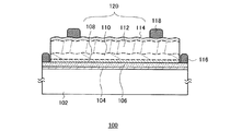
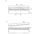
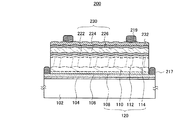
図1に、本形態に係る光電変換装置100の断面の模式図を示す。また、図2に、本形態に係る光電変換装置100の上面の模式図を示す。なお、図1は、図2中のO−P切断線に対応する断面図の一例である。
本形態では、上記実施の形態1と異なる光電変換装置の製造方法の例について説明する。具体的には、上記実施の形態1では、脆化層105、第1不純物半導体層108、第1電極106、絶縁層104の形成順序について(1)の例を説明したが、本形態では、(2)〜(4)の例について説明する。なお、脆化層105、第1不純物半導体層108、第1電極106、絶縁層104の形成順序以外については上記実施の形態1に準ずるため、説明は省略する。
本形態では、上記実施の形態1と異なる光電変換装置の製造方法の例について説明する。
本形態では、上記実施の形態1と異なる光電変換装置の製造方法の例について説明する。
本形態では、ユニットセルを複数積層した所謂タンデム型の光電変換装置の例について説明する。本形態では、ユニットセルを2層積層した光電変換装置について説明する。
本形態では、ユニットセルを複数積層した光電変換装置、具体的にはユニットセルを3層積層した所謂スタック型の光電変換装置300を示す。
実施形態1乃至6により得られる光電変換装置を用いて太陽光発電モジュールを製造することができる。本実施の形態では、上記実施の形態1に示す光電変換装置を用いた太陽光発電モジュールの一例を図24(A)に示す。太陽光発電モジュール1028は、支持基板102の一面上に設けられたユニットセル120により構成されている。支持基板102とユニットセル120との間には、支持基板102側から絶縁層104、第1電極106が設けられている。第1電極106は補助電極116と接続している。
図25は上記実施の形態7で示した太陽光発電モジュール1028を用いた太陽光発電システムの一例を示す。一又は複数の太陽光発電モジュール1028の出力電力は、充電制御回路1029により蓄電池1030を充電する。蓄電池1030の充電量が多い場合には、負荷1031に直接出力される場合もある。
101 単結晶半導体基板
102 支持基板
103 単結晶半導体基板
104 絶縁層
105 脆化層
106 第1電極
107 保護層
108 第1不純物半導体層
109 剥離基板
110 第1単結晶半導体層
111 非晶質半導体層
112 第2単結晶半導体層
113 非晶質半導体層
114 第2不純物半導体層
116 補助電極
118 第2電極
Claims (7)
- 単結晶半導体基板上に、第1電極を形成し、
前記第1電極を介して前記単結晶半導体基板にイオン又はクラスターイオンを照射することにより脆化層を、前記第1電極を介して前記単結晶半導体基板に不純物元素を添加することにより第1不純物半導体層を、それぞれ形成し、
前記第1電極上に、絶縁層を形成し、
前記絶縁層と支持基板とを重ね合わせて貼り合わせた後、前記脆化層又は前記脆化層の近傍を分離面として前記単結晶半導体基板を分離させることにより、前記支持基板上に第1単結晶半導体層を形成し、
シラン系ガスと水素との混合ガスを原料ガスとして、プラズマ化学気相成長法により、前記第1単結晶半導体層上に半導体層をエピタキシャル成長させて第2単結晶半導体層を形成し、
シラン系ガスと水素との混合ガスと、一導電型を付与する不純物元素を含むドーピングガスと、を原料ガスとして、プラズマ化学気相成長法により、前記第2単結晶半導体層上に半導体層をエピタキシャル成長させて、前記第1不純物半導体層とは逆の導電型を有する第2不純物半導体層を形成し、
前記第2不純物半導体層上に、第2電極を形成することを特徴とする光電変換装置の製造方法。 - 単結晶半導体基板上に、第1電極を形成し、
前記第1電極を介して前記単結晶半導体基板にイオン又はクラスターイオンを照射することにより脆化層を、前記第1電極を介して前記単結晶半導体基板に不純物元素を添加することにより第1不純物半導体層を、それぞれ形成し、
前記第1電極上に、絶縁層を形成し、
前記絶縁層と支持基板とを重ね合わせて貼り合わせた後、前記脆化層又は前記脆化層の近傍を分離面として前記単結晶半導体基板を分離させることにより、前記支持基板上に第1単結晶半導体層を形成し、
シラン系ガスと水素との混合ガスを原料ガスとして、プラズマ化学気相成長法により、前記第1単結晶半導体層上に半導体層をエピタキシャル成長させて第2単結晶半導体層を形成し、
シラン系ガスと水素との混合ガスと、一導電型を付与する不純物元素を含むドーピングガスと、を原料ガスとして、プラズマ化学気相成長法により、前記第2単結晶半導体層上に半導体層をエピタキシャル成長させて、前記第1不純物半導体層とは逆の導電型を有する第2不純物半導体層を形成し、
前記第2不純物半導体層上に、前記第2不純物半導体層とは逆の導電型を有する第3不純物半導体層を形成し、
前記第3不純物半導体層上に、非単結晶半導体層を形成し、
前記非単結晶半導体層上に、前記第3不純物半導体層とは逆の導電型を有する第4不純物半導体層を形成し、
前記第4不純物半導体層上に、第2電極を形成することを特徴とする光電変換装置の製造方法。 - 単結晶半導体基板上に、第1電極を形成し、
前記第1電極を介して前記単結晶半導体基板にイオン又はクラスターイオンを照射することにより脆化層を、前記第1電極を介して前記単結晶半導体基板に不純物元素を添加することにより第1不純物半導体層を、それぞれ形成し、
前記第1電極上に、絶縁層を形成し、
前記絶縁層と支持基板とを重ね合わせて貼り合わせた後、前記脆化層又は前記脆化層の近傍を分離面として前記単結晶半導体基板を分離させることにより、前記支持基板上に第1単結晶半導体層を形成し、
シラン系ガスと水素との混合ガスを原料ガスとして、プラズマ化学気相成長法により、前記第1単結晶半導体層上に半導体層をエピタキシャル成長させて第2単結晶半導体層を形成し、
シラン系ガスと水素との混合ガスと、一導電型を付与する不純物元素を含むドーピングガスと、を原料ガスとして、プラズマ化学気相成長法により、前記第2単結晶半導体層上に半導体層をエピタキシャル成長させて、前記第1不純物半導体層とは逆の導電型を有する第2不純物半導体層を形成し、
前記第2不純物半導体層上に、前記第2不純物半導体層とは逆の導電型を有する第3不純物半導体層を形成し、
前記第3不純物半導体層上に、第1非単結晶半導体層を形成し、
前記第1非単結晶半導体層上に、前記第3不純物半導体層とは逆の導電型を有する第4不純物半導体層を形成し、
前記第4不純物半導体層上に、前記第4不純物半導体層とは逆の導電型を有する第5不純物半導体層を形成し、
前記第5不純物半導体層上に、第2非単結晶半導体層を形成し、
前記第2非単結晶半導体層上に、前記第5不純物半導体層とは逆の導電型を有する第6不純物半導体層を形成し、
前記第6不純物半導体層上に、第2電極を形成することを特徴とする光電変換装置の製造方法。 - 請求項3において、
前記第2非単結晶半導体層のエネルギーギャップは、前記第1非単結晶半導体層のエネルギーギャップよりも大きいことを特徴とする光電変換装置の製造方法。 - 請求項1乃至請求項4のいずれか一において、
前記ドーピングガスとして、ジボラン又はフォスフィンを用いることを特徴とする光電変換装置の製造方法。 - 請求項1乃至請求項5のいずれか一において、
前記脆化層の形成には、水素を含む原料ガスにより生成されるイオン又はクラスターイオンを用い、
前記イオン又はクラスターイオンは、生成されたイオンを質量分離しないで電圧で加速して、前記単結晶半導体基板に照射することを特徴とする光電変換装置の製造方法。 - 請求項6において、
前記イオン又はクラスターイオンは、H 3 +イオンを含むことを特徴とする光電変換装置の製造方法。
Priority Applications (1)
| Application Number | Priority Date | Filing Date | Title |
|---|---|---|---|
| JP2008294261A JP5248994B2 (ja) | 2007-11-30 | 2008-11-18 | 光電変換装置の製造方法 |
Applications Claiming Priority (3)
| Application Number | Priority Date | Filing Date | Title |
|---|---|---|---|
| JP2007310817 | 2007-11-30 | ||
| JP2007310817 | 2007-11-30 | ||
| JP2008294261A JP5248994B2 (ja) | 2007-11-30 | 2008-11-18 | 光電変換装置の製造方法 |
Publications (3)
| Publication Number | Publication Date |
|---|---|
| JP2009152566A JP2009152566A (ja) | 2009-07-09 |
| JP2009152566A5 JP2009152566A5 (ja) | 2012-01-05 |
| JP5248994B2 true JP5248994B2 (ja) | 2013-07-31 |
Family
ID=40459831
Family Applications (1)
| Application Number | Title | Priority Date | Filing Date |
|---|---|---|---|
| JP2008294261A Expired - Fee Related JP5248994B2 (ja) | 2007-11-30 | 2008-11-18 | 光電変換装置の製造方法 |
Country Status (4)
| Country | Link |
|---|---|
| US (1) | US7985604B2 (ja) |
| EP (1) | EP2065946A2 (ja) |
| JP (1) | JP5248994B2 (ja) |
| KR (1) | KR101483417B1 (ja) |
Families Citing this family (25)
| Publication number | Priority date | Publication date | Assignee | Title |
|---|---|---|---|---|
| JP5248995B2 (ja) * | 2007-11-30 | 2013-07-31 | 株式会社半導体エネルギー研究所 | 光電変換装置の製造方法 |
| EP2075850A3 (en) * | 2007-12-28 | 2011-08-24 | Semiconductor Energy Laboratory Co, Ltd. | Photoelectric conversion device and manufacturing method thereof |
| JP5572307B2 (ja) * | 2007-12-28 | 2014-08-13 | 株式会社半導体エネルギー研究所 | 光電変換装置の製造方法 |
| KR20100138879A (ko) * | 2008-01-16 | 2010-12-31 | 고꾸리쯔 다이가꾸호우징 도쿄노우코우다이가쿠 | Al계 Ⅲ족 질화물 단결정층을 갖는 적층체의 제조 방법, 그 제법으로 제조되는 적층체, 그 적층체를 사용한 Al계 Ⅲ족 질화물 단결정 기판의 제조 방법, 및, 질화알루미늄 단결정 기판 |
| US8017429B2 (en) | 2008-02-19 | 2011-09-13 | Semiconductor Energy Laboratory Co., Ltd. | Method for manufacturing photoelectric conversion device |
| JP5654206B2 (ja) * | 2008-03-26 | 2015-01-14 | 株式会社半導体エネルギー研究所 | Soi基板の作製方法及び該soi基板を用いた半導体装置 |
| US8338218B2 (en) * | 2008-06-26 | 2012-12-25 | Semiconductor Energy Laboratory Co., Ltd. | Photoelectric conversion device module and manufacturing method of the photoelectric conversion device module |
| JP5552276B2 (ja) * | 2008-08-01 | 2014-07-16 | 株式会社半導体エネルギー研究所 | Soi基板の作製方法 |
| SG182208A1 (en) * | 2008-12-15 | 2012-07-30 | Semiconductor Energy Lab | Manufacturing method of soi substrate and manufacturing method of semiconductor device |
| JP5706670B2 (ja) | 2009-11-24 | 2015-04-22 | 株式会社半導体エネルギー研究所 | Soi基板の作製方法 |
| US8704083B2 (en) | 2010-02-11 | 2014-04-22 | Semiconductor Energy Laboratory Co., Ltd. | Photoelectric conversion device and fabrication method thereof |
| KR101112494B1 (ko) * | 2010-03-17 | 2012-03-13 | 한국과학기술원 | 광기전력 장치의 제조 방법 |
| NO20100616A1 (no) * | 2010-04-28 | 2011-10-31 | Innotech Solar Asa | Fremgangsmate og anordning for a fjerne en defekt fra en solcelle |
| JP5755931B2 (ja) | 2010-04-28 | 2015-07-29 | 株式会社半導体エネルギー研究所 | 半導体膜の作製方法、電極の作製方法、2次電池の作製方法、および太陽電池の作製方法 |
| US8173452B1 (en) * | 2010-12-29 | 2012-05-08 | Twin Creeks Technologies, Inc. | Method to form a device by constructing a support element on a thin semiconductor lamina |
| EP2659521A4 (en) * | 2010-12-29 | 2015-05-13 | Gtat Corp | METHOD AND APPARATUS FOR FORMING A FINE LAMINA |
| US8536448B2 (en) | 2010-12-29 | 2013-09-17 | Gtat Corporation | Zener diode within a diode structure providing shunt protection |
| CN103348491A (zh) * | 2010-12-29 | 2013-10-09 | Gtat公司 | 通过在薄的半导体薄片上构造支撑元件而形成设备的方法 |
| US8435804B2 (en) | 2010-12-29 | 2013-05-07 | Gtat Corporation | Method and apparatus for forming a thin lamina |
| US8268645B2 (en) | 2010-12-29 | 2012-09-18 | Twin Creeks Technologies, Inc. | Method and apparatus for forming a thin lamina |
| JP2013058562A (ja) | 2011-09-07 | 2013-03-28 | Semiconductor Energy Lab Co Ltd | 光電変換装置 |
| US8916954B2 (en) * | 2012-02-05 | 2014-12-23 | Gtat Corporation | Multi-layer metal support |
| US8841161B2 (en) | 2012-02-05 | 2014-09-23 | GTAT.Corporation | Method for forming flexible solar cells |
| US8785294B2 (en) | 2012-07-26 | 2014-07-22 | Gtat Corporation | Silicon carbide lamina |
| JP6459948B2 (ja) * | 2015-12-15 | 2019-01-30 | 株式会社Sumco | 半導体エピタキシャルウェーハの製造方法および固体撮像素子の製造方法 |
Family Cites Families (47)
| Publication number | Priority date | Publication date | Assignee | Title |
|---|---|---|---|---|
| US4180618A (en) * | 1977-07-27 | 1979-12-25 | Corning Glass Works | Thin silicon film electronic device |
| DE3177084D1 (en) * | 1980-04-10 | 1989-09-21 | Massachusetts Inst Technology | Method of producing sheets of crystalline material |
| JPS57160179A (en) * | 1981-03-28 | 1982-10-02 | Tdk Corp | Photodiode device and manufacture thereof |
| JPH0644638B2 (ja) | 1982-12-29 | 1994-06-08 | 圭弘 濱川 | 異質単位セル同士のスタック形光起電力素子 |
| US4496788A (en) * | 1982-12-29 | 1985-01-29 | Osaka Transformer Co., Ltd. | Photovoltaic device |
| US4633034A (en) * | 1985-02-08 | 1986-12-30 | Energy Conversion Devices, Inc. | Photovoltaic device and method |
| JPS63196082A (ja) * | 1987-02-10 | 1988-08-15 | Toa Nenryo Kogyo Kk | 太陽電池の製造方法 |
| US5750000A (en) * | 1990-08-03 | 1998-05-12 | Canon Kabushiki Kaisha | Semiconductor member, and process for preparing same and semiconductor device formed by use of same |
| ATE217447T1 (de) * | 1990-08-03 | 2002-05-15 | Canon Kk | Verfahren zur herstellung eines halbleiterkörpers |
| CA2069038C (en) * | 1991-05-22 | 1997-08-12 | Kiyofumi Sakaguchi | Method for preparing semiconductor member |
| JPH0644638A (ja) | 1992-07-24 | 1994-02-18 | Sony Corp | 録音装置 |
| JP3360919B2 (ja) * | 1993-06-11 | 2003-01-07 | 三菱電機株式会社 | 薄膜太陽電池の製造方法,及び薄膜太陽電池 |
| JP3352340B2 (ja) * | 1995-10-06 | 2002-12-03 | キヤノン株式会社 | 半導体基体とその製造方法 |
| JP3381443B2 (ja) * | 1995-02-02 | 2003-02-24 | ソニー株式会社 | 基体から半導体層を分離する方法、半導体素子の製造方法およびsoi基板の製造方法 |
| US5736431A (en) * | 1995-02-28 | 1998-04-07 | Semiconductor Energy Laboratory Co., Ltd. | Method for producing thin film solar battery |
| JPH08255762A (ja) * | 1995-03-17 | 1996-10-01 | Nec Corp | 半導体デバイスの製造方法 |
| JPH1093122A (ja) * | 1996-09-10 | 1998-04-10 | Nippon Telegr & Teleph Corp <Ntt> | 薄膜太陽電池の製造方法 |
| DE69738307T2 (de) * | 1996-12-27 | 2008-10-02 | Canon K.K. | Herstellungsverfahren eines Halbleiter-Bauelements und Herstellungsverfahren einer Solarzelle |
| JPH10335683A (ja) * | 1997-05-28 | 1998-12-18 | Ion Kogaku Kenkyusho:Kk | タンデム型太陽電池およびその製造方法 |
| JPH1197379A (ja) | 1997-07-25 | 1999-04-09 | Denso Corp | 半導体基板及び半導体基板の製造方法 |
| US6534380B1 (en) * | 1997-07-18 | 2003-03-18 | Denso Corporation | Semiconductor substrate and method of manufacturing the same |
| JPH11163363A (ja) | 1997-11-22 | 1999-06-18 | Semiconductor Energy Lab Co Ltd | 半導体装置およびその作製方法 |
| US6331208B1 (en) * | 1998-05-15 | 2001-12-18 | Canon Kabushiki Kaisha | Process for producing solar cell, process for producing thin-film semiconductor, process for separating thin-film semiconductor, and process for forming semiconductor |
| JP2000012864A (ja) * | 1998-06-22 | 2000-01-14 | Semiconductor Energy Lab Co Ltd | 半導体装置の作製方法 |
| JP2000124092A (ja) * | 1998-10-16 | 2000-04-28 | Shin Etsu Handotai Co Ltd | 水素イオン注入剥離法によってsoiウエーハを製造する方法およびこの方法で製造されたsoiウエーハ |
| JP2000150940A (ja) * | 1998-11-18 | 2000-05-30 | Denso Corp | 半導体微粒子集合体及びその製造方法 |
| JP2000349264A (ja) * | 1998-12-04 | 2000-12-15 | Canon Inc | 半導体ウエハの製造方法、使用方法および利用方法 |
| JP2000349266A (ja) * | 1999-03-26 | 2000-12-15 | Canon Inc | 半導体部材の製造方法、半導体基体の利用方法、半導体部材の製造システム、半導体部材の生産管理方法及び堆積膜形成装置の利用方法 |
| JP2001015721A (ja) * | 1999-04-30 | 2001-01-19 | Canon Inc | 複合部材の分離方法及び薄膜の製造方法 |
| US6387829B1 (en) * | 1999-06-18 | 2002-05-14 | Silicon Wafer Technologies, Inc. | Separation process for silicon-on-insulator wafer fabrication |
| JP4452789B2 (ja) * | 1999-09-01 | 2010-04-21 | 独立行政法人 日本原子力研究開発機構 | シリコン系結晶薄板の製造方法および光電変換素子用基板の製造方法 |
| JP2001160540A (ja) * | 1999-09-22 | 2001-06-12 | Canon Inc | 半導体装置の製造方法、液相成長法及び液相成長装置、太陽電池 |
| JP2001127313A (ja) * | 1999-10-25 | 2001-05-11 | Sony Corp | 薄膜半導体素子およびその製造方法 |
| JP3513592B2 (ja) * | 2000-09-25 | 2004-03-31 | 独立行政法人産業技術総合研究所 | 太陽電池の製造方法 |
| JP2002348198A (ja) | 2001-05-28 | 2002-12-04 | Nissin Electric Co Ltd | 半導体素子エピタキシャル成長用基板及びその製造方法 |
| US6818529B2 (en) * | 2002-09-12 | 2004-11-16 | Applied Materials, Inc. | Apparatus and method for forming a silicon film across the surface of a glass substrate |
| JP2005268682A (ja) | 2004-03-22 | 2005-09-29 | Canon Inc | 半導体基材及び太陽電池の製造方法 |
| EP2002484A4 (en) * | 2006-04-05 | 2016-06-08 | Silicon Genesis Corp | METHOD AND STRUCTURE FOR MANUFACTURING PHOTOVOLTAIC CELLS USING A LAYER TRANSFER PROCESS |
| JP2007310817A (ja) | 2006-05-22 | 2007-11-29 | Sharp Corp | 追加認証方法及び認証装置 |
| JP2008112847A (ja) * | 2006-10-30 | 2008-05-15 | Shin Etsu Chem Co Ltd | 単結晶シリコン太陽電池の製造方法及び単結晶シリコン太陽電池 |
| EP2135295A4 (en) * | 2007-04-06 | 2014-05-21 | Semiconductor Energy Lab | Photovoltaic module and method for its production |
| CN101657907B (zh) * | 2007-04-13 | 2012-12-26 | 株式会社半导体能源研究所 | 光伏器件及其制造方法 |
| JP5459899B2 (ja) * | 2007-06-01 | 2014-04-02 | 株式会社半導体エネルギー研究所 | 半導体装置の作製方法 |
| KR101608953B1 (ko) * | 2007-11-09 | 2016-04-04 | 가부시키가이샤 한도오따이 에네루기 켄큐쇼 | 광전 변환 장치 및 그 제조 방법 |
| TWI452703B (zh) * | 2007-11-16 | 2014-09-11 | Semiconductor Energy Lab | 光電轉換裝置及其製造方法 |
| JP5248995B2 (ja) * | 2007-11-30 | 2013-07-31 | 株式会社半導体エネルギー研究所 | 光電変換装置の製造方法 |
| JP5286046B2 (ja) * | 2007-11-30 | 2013-09-11 | 株式会社半導体エネルギー研究所 | 光電変換装置の製造方法 |
-
2008
- 2008-11-18 JP JP2008294261A patent/JP5248994B2/ja not_active Expired - Fee Related
- 2008-11-26 EP EP08020573A patent/EP2065946A2/en not_active Withdrawn
- 2008-11-26 US US12/324,065 patent/US7985604B2/en not_active Expired - Fee Related
- 2008-11-28 KR KR20080119602A patent/KR101483417B1/ko active IP Right Grant
Also Published As
| Publication number | Publication date |
|---|---|
| EP2065946A2 (en) | 2009-06-03 |
| JP2009152566A (ja) | 2009-07-09 |
| US7985604B2 (en) | 2011-07-26 |
| US20090142908A1 (en) | 2009-06-04 |
| KR101483417B1 (ko) | 2015-01-16 |
| KR20090056899A (ko) | 2009-06-03 |
Similar Documents
| Publication | Publication Date | Title |
|---|---|---|
| JP5248994B2 (ja) | 光電変換装置の製造方法 | |
| JP5248995B2 (ja) | 光電変換装置の製造方法 | |
| JP5572307B2 (ja) | 光電変換装置の製造方法 | |
| JP5352190B2 (ja) | 光電変換装置 | |
| JP5286046B2 (ja) | 光電変換装置の製造方法 | |
| JP5286146B2 (ja) | 光電変換装置の作製方法 | |
| US8338218B2 (en) | Photoelectric conversion device module and manufacturing method of the photoelectric conversion device module | |
| JP5315008B2 (ja) | 光電変換装置 | |
| JP5577030B2 (ja) | 光電変換装置及びその製造方法 | |
| US8017429B2 (en) | Method for manufacturing photoelectric conversion device | |
| JP5723204B2 (ja) | 半導体基板の作製方法 |
Legal Events
| Date | Code | Title | Description |
|---|---|---|---|
| A521 | Request for written amendment filed |
Free format text: JAPANESE INTERMEDIATE CODE: A523 Effective date: 20111114 |
|
| A621 | Written request for application examination |
Free format text: JAPANESE INTERMEDIATE CODE: A621 Effective date: 20111114 |
|
| A977 | Report on retrieval |
Free format text: JAPANESE INTERMEDIATE CODE: A971007 Effective date: 20121128 |
|
| A131 | Notification of reasons for refusal |
Free format text: JAPANESE INTERMEDIATE CODE: A131 Effective date: 20121204 |
|
| A521 | Request for written amendment filed |
Free format text: JAPANESE INTERMEDIATE CODE: A523 Effective date: 20130111 |
|
| TRDD | Decision of grant or rejection written | ||
| A01 | Written decision to grant a patent or to grant a registration (utility model) |
Free format text: JAPANESE INTERMEDIATE CODE: A01 Effective date: 20130402 |
|
| A61 | First payment of annual fees (during grant procedure) |
Free format text: JAPANESE INTERMEDIATE CODE: A61 Effective date: 20130411 |
|
| R150 | Certificate of patent or registration of utility model |
Free format text: JAPANESE INTERMEDIATE CODE: R150 |
|
| FPAY | Renewal fee payment (event date is renewal date of database) |
Free format text: PAYMENT UNTIL: 20160419 Year of fee payment: 3 |
|
| R250 | Receipt of annual fees |
Free format text: JAPANESE INTERMEDIATE CODE: R250 |
|
| R250 | Receipt of annual fees |
Free format text: JAPANESE INTERMEDIATE CODE: R250 |
|
| LAPS | Cancellation because of no payment of annual fees |