JP5572307B2 - 光電変換装置の製造方法 - Google Patents
光電変換装置の製造方法 Download PDFInfo
- Publication number
- JP5572307B2 JP5572307B2 JP2008319106A JP2008319106A JP5572307B2 JP 5572307 B2 JP5572307 B2 JP 5572307B2 JP 2008319106 A JP2008319106 A JP 2008319106A JP 2008319106 A JP2008319106 A JP 2008319106A JP 5572307 B2 JP5572307 B2 JP 5572307B2
- Authority
- JP
- Japan
- Prior art keywords
- single crystal
- layer
- crystal silicon
- silicon layer
- electrode
- Prior art date
- Legal status (The legal status is an assumption and is not a legal conclusion. Google has not performed a legal analysis and makes no representation as to the accuracy of the status listed.)
- Expired - Fee Related
Links
- 238000006243 chemical reaction Methods 0.000 title claims description 160
- 238000000034 method Methods 0.000 title claims description 57
- 238000004519 manufacturing process Methods 0.000 title claims description 35
- 229910021421 monocrystalline silicon Inorganic materials 0.000 claims description 405
- 239000000758 substrate Substances 0.000 claims description 325
- 229910052710 silicon Inorganic materials 0.000 claims description 232
- XUIMIQQOPSSXEZ-UHFFFAOYSA-N Silicon Chemical compound [Si] XUIMIQQOPSSXEZ-UHFFFAOYSA-N 0.000 claims description 230
- 239000010703 silicon Substances 0.000 claims description 230
- 239000012535 impurity Substances 0.000 claims description 222
- 150000002500 ions Chemical class 0.000 claims description 102
- 239000013078 crystal Substances 0.000 claims description 70
- 230000007547 defect Effects 0.000 claims description 59
- 238000010438 heat treatment Methods 0.000 claims description 34
- BLRPTPMANUNPDV-UHFFFAOYSA-N Silane Chemical compound [SiH4] BLRPTPMANUNPDV-UHFFFAOYSA-N 0.000 claims description 28
- 229910000077 silane Inorganic materials 0.000 claims description 27
- 230000008569 process Effects 0.000 claims description 16
- 230000001678 irradiating effect Effects 0.000 claims description 13
- 239000011521 glass Substances 0.000 claims description 9
- 230000008439 repair process Effects 0.000 claims description 9
- 239000010410 layer Substances 0.000 description 716
- 239000007789 gas Substances 0.000 description 113
- 239000001257 hydrogen Substances 0.000 description 39
- 229910052739 hydrogen Inorganic materials 0.000 description 39
- 238000005268 plasma chemical vapour deposition Methods 0.000 description 37
- UFHFLCQGNIYNRP-UHFFFAOYSA-N Hydrogen Chemical compound [H][H] UFHFLCQGNIYNRP-UHFFFAOYSA-N 0.000 description 34
- 238000000926 separation method Methods 0.000 description 34
- IJGRMHOSHXDMSA-UHFFFAOYSA-N Atomic nitrogen Chemical compound N#N IJGRMHOSHXDMSA-UHFFFAOYSA-N 0.000 description 33
- 239000011241 protective layer Substances 0.000 description 32
- 239000010408 film Substances 0.000 description 25
- 230000015572 biosynthetic process Effects 0.000 description 22
- 238000011282 treatment Methods 0.000 description 22
- 229910021417 amorphous silicon Inorganic materials 0.000 description 19
- 125000004429 atom Chemical group 0.000 description 19
- 238000005530 etching Methods 0.000 description 18
- 239000004065 semiconductor Substances 0.000 description 17
- 229910052581 Si3N4 Inorganic materials 0.000 description 16
- HQVNEWCFYHHQES-UHFFFAOYSA-N silicon nitride Chemical compound N12[Si]34N5[Si]62N3[Si]51N64 HQVNEWCFYHHQES-UHFFFAOYSA-N 0.000 description 16
- XLYOFNOQVPJJNP-UHFFFAOYSA-N water Substances O XLYOFNOQVPJJNP-UHFFFAOYSA-N 0.000 description 16
- 238000010586 diagram Methods 0.000 description 14
- 229910021424 microcrystalline silicon Inorganic materials 0.000 description 13
- 229910052757 nitrogen Inorganic materials 0.000 description 13
- 230000006798 recombination Effects 0.000 description 13
- 230000002829 reductive effect Effects 0.000 description 13
- 230000003746 surface roughness Effects 0.000 description 13
- 239000000463 material Substances 0.000 description 12
- 239000002994 raw material Substances 0.000 description 12
- 238000004140 cleaning Methods 0.000 description 11
- 238000002347 injection Methods 0.000 description 11
- 239000007924 injection Substances 0.000 description 11
- 238000010884 ion-beam technique Methods 0.000 description 11
- 238000010248 power generation Methods 0.000 description 11
- PXHVJJICTQNCMI-UHFFFAOYSA-N Nickel Chemical compound [Ni] PXHVJJICTQNCMI-UHFFFAOYSA-N 0.000 description 10
- 239000000969 carrier Substances 0.000 description 10
- 238000005468 ion implantation Methods 0.000 description 10
- 238000013532 laser treatment Methods 0.000 description 10
- 238000002161 passivation Methods 0.000 description 10
- 238000005498 polishing Methods 0.000 description 10
- 230000001133 acceleration Effects 0.000 description 9
- 230000006870 function Effects 0.000 description 9
- 239000001301 oxygen Substances 0.000 description 9
- 229910052760 oxygen Inorganic materials 0.000 description 9
- 229910021420 polycrystalline silicon Inorganic materials 0.000 description 9
- XKRFYHLGVUSROY-UHFFFAOYSA-N Argon Chemical compound [Ar] XKRFYHLGVUSROY-UHFFFAOYSA-N 0.000 description 8
- ZOXJGFHDIHLPTG-UHFFFAOYSA-N Boron Chemical compound [B] ZOXJGFHDIHLPTG-UHFFFAOYSA-N 0.000 description 8
- KRHYYFGTRYWZRS-UHFFFAOYSA-N Fluorane Chemical compound F KRHYYFGTRYWZRS-UHFFFAOYSA-N 0.000 description 8
- XYFCBTPGUUZFHI-UHFFFAOYSA-N Phosphine Chemical compound P XYFCBTPGUUZFHI-UHFFFAOYSA-N 0.000 description 8
- QVGXLLKOCUKJST-UHFFFAOYSA-N atomic oxygen Chemical compound [O] QVGXLLKOCUKJST-UHFFFAOYSA-N 0.000 description 8
- 229910052796 boron Inorganic materials 0.000 description 8
- 238000000605 extraction Methods 0.000 description 8
- 238000005229 chemical vapour deposition Methods 0.000 description 7
- 229910001873 dinitrogen Inorganic materials 0.000 description 7
- 238000002844 melting Methods 0.000 description 7
- 230000008018 melting Effects 0.000 description 7
- VYPSYNLAJGMNEJ-UHFFFAOYSA-N silicon dioxide Inorganic materials O=[Si]=O VYPSYNLAJGMNEJ-UHFFFAOYSA-N 0.000 description 7
- CURLTUGMZLYLDI-UHFFFAOYSA-N Carbon dioxide Chemical compound O=C=O CURLTUGMZLYLDI-UHFFFAOYSA-N 0.000 description 6
- 238000005215 recombination Methods 0.000 description 6
- 229910052814 silicon oxide Inorganic materials 0.000 description 6
- 239000002344 surface layer Substances 0.000 description 6
- WGTYBPLFGIVFAS-UHFFFAOYSA-M tetramethylammonium hydroxide Chemical compound [OH-].C[N+](C)(C)C WGTYBPLFGIVFAS-UHFFFAOYSA-M 0.000 description 6
- 238000001039 wet etching Methods 0.000 description 6
- 239000012298 atmosphere Substances 0.000 description 5
- 239000001307 helium Substances 0.000 description 5
- 229910052734 helium Inorganic materials 0.000 description 5
- SWQJXJOGLNCZEY-UHFFFAOYSA-N helium atom Chemical compound [He] SWQJXJOGLNCZEY-UHFFFAOYSA-N 0.000 description 5
- 229910052759 nickel Inorganic materials 0.000 description 5
- 230000003287 optical effect Effects 0.000 description 5
- 230000001443 photoexcitation Effects 0.000 description 5
- 239000000126 substance Substances 0.000 description 5
- QGZKDVFQNNGYKY-UHFFFAOYSA-N Ammonia Chemical compound N QGZKDVFQNNGYKY-UHFFFAOYSA-N 0.000 description 4
- BQCADISMDOOEFD-UHFFFAOYSA-N Silver Chemical compound [Ag] BQCADISMDOOEFD-UHFFFAOYSA-N 0.000 description 4
- XLOMVQKBTHCTTD-UHFFFAOYSA-N Zinc monoxide Chemical compound [Zn]=O XLOMVQKBTHCTTD-UHFFFAOYSA-N 0.000 description 4
- 229910052786 argon Inorganic materials 0.000 description 4
- PZPGRFITIJYNEJ-UHFFFAOYSA-N disilane Chemical compound [SiH3][SiH3] PZPGRFITIJYNEJ-UHFFFAOYSA-N 0.000 description 4
- 238000001312 dry etching Methods 0.000 description 4
- 230000000694 effects Effects 0.000 description 4
- GPRLSGONYQIRFK-UHFFFAOYSA-N hydron Chemical compound [H+] GPRLSGONYQIRFK-UHFFFAOYSA-N 0.000 description 4
- 230000005660 hydrophilic surface Effects 0.000 description 4
- 150000004767 nitrides Chemical class 0.000 description 4
- 229910000073 phosphorus hydride Inorganic materials 0.000 description 4
- 238000007650 screen-printing Methods 0.000 description 4
- 229910052709 silver Inorganic materials 0.000 description 4
- 239000004332 silver Substances 0.000 description 4
- 238000004544 sputter deposition Methods 0.000 description 4
- 238000003860 storage Methods 0.000 description 4
- 239000010409 thin film Substances 0.000 description 4
- 244000126211 Hericium coralloides Species 0.000 description 3
- OAICVXFJPJFONN-UHFFFAOYSA-N Phosphorus Chemical compound [P] OAICVXFJPJFONN-UHFFFAOYSA-N 0.000 description 3
- BOTDANWDWHJENH-UHFFFAOYSA-N Tetraethyl orthosilicate Chemical compound CCO[Si](OCC)(OCC)OCC BOTDANWDWHJENH-UHFFFAOYSA-N 0.000 description 3
- RTAQQCXQSZGOHL-UHFFFAOYSA-N Titanium Chemical compound [Ti] RTAQQCXQSZGOHL-UHFFFAOYSA-N 0.000 description 3
- 229910052782 aluminium Inorganic materials 0.000 description 3
- XAGFODPZIPBFFR-UHFFFAOYSA-N aluminium Chemical compound [Al] XAGFODPZIPBFFR-UHFFFAOYSA-N 0.000 description 3
- 239000001569 carbon dioxide Substances 0.000 description 3
- 229910002092 carbon dioxide Inorganic materials 0.000 description 3
- 230000008859 change Effects 0.000 description 3
- 229920001940 conductive polymer Polymers 0.000 description 3
- 239000004020 conductor Substances 0.000 description 3
- 229910021419 crystalline silicon Inorganic materials 0.000 description 3
- 238000000151 deposition Methods 0.000 description 3
- 230000008021 deposition Effects 0.000 description 3
- 238000001678 elastic recoil detection analysis Methods 0.000 description 3
- 125000004435 hydrogen atom Chemical group [H]* 0.000 description 3
- 239000011261 inert gas Substances 0.000 description 3
- 239000007791 liquid phase Substances 0.000 description 3
- 229910052751 metal Inorganic materials 0.000 description 3
- 239000002184 metal Substances 0.000 description 3
- 239000007769 metal material Substances 0.000 description 3
- 239000000203 mixture Substances 0.000 description 3
- 230000004048 modification Effects 0.000 description 3
- 238000012986 modification Methods 0.000 description 3
- 229910052698 phosphorus Inorganic materials 0.000 description 3
- 239000011574 phosphorus Substances 0.000 description 3
- 238000007639 printing Methods 0.000 description 3
- 238000005001 rutherford backscattering spectroscopy Methods 0.000 description 3
- 229910052719 titanium Inorganic materials 0.000 description 3
- 239000010936 titanium Substances 0.000 description 3
- 229910052721 tungsten Inorganic materials 0.000 description 3
- 239000010937 tungsten Substances 0.000 description 3
- WZJUBBHODHNQPW-UHFFFAOYSA-N 2,4,6,8-tetramethyl-1,3,5,7,2$l^{3},4$l^{3},6$l^{3},8$l^{3}-tetraoxatetrasilocane Chemical compound C[Si]1O[Si](C)O[Si](C)O[Si](C)O1 WZJUBBHODHNQPW-UHFFFAOYSA-N 0.000 description 2
- OKTJSMMVPCPJKN-UHFFFAOYSA-N Carbon Chemical compound [C] OKTJSMMVPCPJKN-UHFFFAOYSA-N 0.000 description 2
- YCKRFDGAMUMZLT-UHFFFAOYSA-N Fluorine atom Chemical compound [F] YCKRFDGAMUMZLT-UHFFFAOYSA-N 0.000 description 2
- GQPLMRYTRLFLPF-UHFFFAOYSA-N Nitrous Oxide Chemical compound [O-][N+]#N GQPLMRYTRLFLPF-UHFFFAOYSA-N 0.000 description 2
- CBENFWSGALASAD-UHFFFAOYSA-N Ozone Chemical compound [O-][O+]=O CBENFWSGALASAD-UHFFFAOYSA-N 0.000 description 2
- 238000005411 Van der Waals force Methods 0.000 description 2
- 229910021529 ammonia Inorganic materials 0.000 description 2
- 229910052785 arsenic Inorganic materials 0.000 description 2
- RQNWIZPPADIBDY-UHFFFAOYSA-N arsenic atom Chemical compound [As] RQNWIZPPADIBDY-UHFFFAOYSA-N 0.000 description 2
- 230000000903 blocking effect Effects 0.000 description 2
- 229910052799 carbon Inorganic materials 0.000 description 2
- 238000005520 cutting process Methods 0.000 description 2
- 230000002542 deteriorative effect Effects 0.000 description 2
- 238000009792 diffusion process Methods 0.000 description 2
- 230000005611 electricity Effects 0.000 description 2
- 238000007667 floating Methods 0.000 description 2
- 229910052731 fluorine Inorganic materials 0.000 description 2
- 239000011737 fluorine Substances 0.000 description 2
- 150000002431 hydrogen Chemical class 0.000 description 2
- QOSATHPSBFQAML-UHFFFAOYSA-N hydrogen peroxide;hydrate Chemical compound O.OO QOSATHPSBFQAML-UHFFFAOYSA-N 0.000 description 2
- 125000002887 hydroxy group Chemical group [H]O* 0.000 description 2
- 238000002513 implantation Methods 0.000 description 2
- 230000006872 improvement Effects 0.000 description 2
- 229910003437 indium oxide Inorganic materials 0.000 description 2
- PJXISJQVUVHSOJ-UHFFFAOYSA-N indium(iii) oxide Chemical compound [O-2].[O-2].[O-2].[In+3].[In+3] PJXISJQVUVHSOJ-UHFFFAOYSA-N 0.000 description 2
- LQBJWKCYZGMFEV-UHFFFAOYSA-N lead tin Chemical compound [Sn].[Pb] LQBJWKCYZGMFEV-UHFFFAOYSA-N 0.000 description 2
- VNWKTOKETHGBQD-UHFFFAOYSA-N methane Chemical compound C VNWKTOKETHGBQD-UHFFFAOYSA-N 0.000 description 2
- 230000010355 oscillation Effects 0.000 description 2
- 230000036961 partial effect Effects 0.000 description 2
- 239000002245 particle Substances 0.000 description 2
- 230000000737 periodic effect Effects 0.000 description 2
- 238000009832 plasma treatment Methods 0.000 description 2
- 239000003870 refractory metal Substances 0.000 description 2
- 230000008929 regeneration Effects 0.000 description 2
- 238000011069 regeneration method Methods 0.000 description 2
- 229910000679 solder Inorganic materials 0.000 description 2
- 239000007790 solid phase Substances 0.000 description 2
- 229910052715 tantalum Inorganic materials 0.000 description 2
- GUVRBAGPIYLISA-UHFFFAOYSA-N tantalum atom Chemical compound [Ta] GUVRBAGPIYLISA-UHFFFAOYSA-N 0.000 description 2
- CZDYPVPMEAXLPK-UHFFFAOYSA-N tetramethylsilane Chemical compound C[Si](C)(C)C CZDYPVPMEAXLPK-UHFFFAOYSA-N 0.000 description 2
- VEDJZFSRVVQBIL-UHFFFAOYSA-N trisilane Chemical compound [SiH3][SiH2][SiH3] VEDJZFSRVVQBIL-UHFFFAOYSA-N 0.000 description 2
- WFKWXMTUELFFGS-UHFFFAOYSA-N tungsten Chemical compound [W] WFKWXMTUELFFGS-UHFFFAOYSA-N 0.000 description 2
- -1 tungsten nitride Chemical class 0.000 description 2
- 238000010792 warming Methods 0.000 description 2
- 239000011787 zinc oxide Substances 0.000 description 2
- VHUUQVKOLVNVRT-UHFFFAOYSA-N Ammonium hydroxide Chemical compound [NH4+].[OH-] VHUUQVKOLVNVRT-UHFFFAOYSA-N 0.000 description 1
- VEXZGXHMUGYJMC-UHFFFAOYSA-M Chloride anion Chemical compound [Cl-] VEXZGXHMUGYJMC-UHFFFAOYSA-M 0.000 description 1
- VYZAMTAEIAYCRO-UHFFFAOYSA-N Chromium Chemical compound [Cr] VYZAMTAEIAYCRO-UHFFFAOYSA-N 0.000 description 1
- KRHYYFGTRYWZRS-UHFFFAOYSA-M Fluoride anion Chemical compound [F-] KRHYYFGTRYWZRS-UHFFFAOYSA-M 0.000 description 1
- DGAQECJNVWCQMB-PUAWFVPOSA-M Ilexoside XXIX Chemical compound C[C@@H]1CC[C@@]2(CC[C@@]3(C(=CC[C@H]4[C@]3(CC[C@@H]5[C@@]4(CC[C@@H](C5(C)C)OS(=O)(=O)[O-])C)C)[C@@H]2[C@]1(C)O)C)C(=O)O[C@H]6[C@@H]([C@H]([C@@H]([C@H](O6)CO)O)O)O.[Na+] DGAQECJNVWCQMB-PUAWFVPOSA-M 0.000 description 1
- ZOKXTWBITQBERF-UHFFFAOYSA-N Molybdenum Chemical compound [Mo] ZOKXTWBITQBERF-UHFFFAOYSA-N 0.000 description 1
- 229910002656 O–Si–O Inorganic materials 0.000 description 1
- SZKKRCSOSQAJDE-UHFFFAOYSA-N Schradan Chemical group CN(C)P(=O)(N(C)C)OP(=O)(N(C)C)N(C)C SZKKRCSOSQAJDE-UHFFFAOYSA-N 0.000 description 1
- 229910008051 Si-OH Inorganic materials 0.000 description 1
- 229910006358 Si—OH Inorganic materials 0.000 description 1
- 229910001128 Sn alloy Inorganic materials 0.000 description 1
- NRTOMJZYCJJWKI-UHFFFAOYSA-N Titanium nitride Chemical class [Ti]#N NRTOMJZYCJJWKI-UHFFFAOYSA-N 0.000 description 1
- 238000010521 absorption reaction Methods 0.000 description 1
- 230000009471 action Effects 0.000 description 1
- 230000004913 activation Effects 0.000 description 1
- 239000000853 adhesive Substances 0.000 description 1
- 230000001070 adhesive effect Effects 0.000 description 1
- 230000002411 adverse Effects 0.000 description 1
- 229910045601 alloy Inorganic materials 0.000 description 1
- 239000000956 alloy Substances 0.000 description 1
- 239000005407 aluminoborosilicate glass Substances 0.000 description 1
- 239000005354 aluminosilicate glass Substances 0.000 description 1
- 235000011114 ammonium hydroxide Nutrition 0.000 description 1
- 239000007864 aqueous solution Substances 0.000 description 1
- 238000001505 atmospheric-pressure chemical vapour deposition Methods 0.000 description 1
- 229910052788 barium Inorganic materials 0.000 description 1
- DSAJWYNOEDNPEQ-UHFFFAOYSA-N barium atom Chemical compound [Ba] DSAJWYNOEDNPEQ-UHFFFAOYSA-N 0.000 description 1
- 238000007664 blowing Methods 0.000 description 1
- 229910052795 boron group element Inorganic materials 0.000 description 1
- 239000005388 borosilicate glass Substances 0.000 description 1
- 239000003990 capacitor Substances 0.000 description 1
- 239000000919 ceramic Substances 0.000 description 1
- 229910052804 chromium Inorganic materials 0.000 description 1
- 239000011651 chromium Substances 0.000 description 1
- 239000003034 coal gas Substances 0.000 description 1
- 238000011109 contamination Methods 0.000 description 1
- 238000001816 cooling Methods 0.000 description 1
- 229920001577 copolymer Polymers 0.000 description 1
- DDJSWKLBKSLAAZ-UHFFFAOYSA-N cyclotetrasiloxane Chemical compound O1[SiH2]O[SiH2]O[SiH2]O[SiH2]1 DDJSWKLBKSLAAZ-UHFFFAOYSA-N 0.000 description 1
- 238000007599 discharging Methods 0.000 description 1
- 239000000428 dust Substances 0.000 description 1
- 238000010891 electric arc Methods 0.000 description 1
- 230000005684 electric field Effects 0.000 description 1
- 238000005401 electroluminescence Methods 0.000 description 1
- 238000005265 energy consumption Methods 0.000 description 1
- 238000005516 engineering process Methods 0.000 description 1
- 238000001704 evaporation Methods 0.000 description 1
- 230000001747 exhibiting effect Effects 0.000 description 1
- 239000000284 extract Substances 0.000 description 1
- 239000012530 fluid Substances 0.000 description 1
- 239000005431 greenhouse gas Substances 0.000 description 1
- 229910052736 halogen Inorganic materials 0.000 description 1
- 150000002367 halogens Chemical class 0.000 description 1
- FFUAGWLWBBFQJT-UHFFFAOYSA-N hexamethyldisilazane Chemical compound C[Si](C)(C)N[Si](C)(C)C FFUAGWLWBBFQJT-UHFFFAOYSA-N 0.000 description 1
- 150000004678 hydrides Chemical class 0.000 description 1
- 238000009413 insulation Methods 0.000 description 1
- 238000005304 joining Methods 0.000 description 1
- 238000010030 laminating Methods 0.000 description 1
- 238000010329 laser etching Methods 0.000 description 1
- 230000031700 light absorption Effects 0.000 description 1
- 239000007788 liquid Substances 0.000 description 1
- 238000004518 low pressure chemical vapour deposition Methods 0.000 description 1
- ORUIBWPALBXDOA-UHFFFAOYSA-L magnesium fluoride Chemical compound [F-].[F-].[Mg+2] ORUIBWPALBXDOA-UHFFFAOYSA-L 0.000 description 1
- 229910001635 magnesium fluoride Inorganic materials 0.000 description 1
- 238000005259 measurement Methods 0.000 description 1
- 239000000155 melt Substances 0.000 description 1
- QSHDDOUJBYECFT-UHFFFAOYSA-N mercury Chemical compound [Hg] QSHDDOUJBYECFT-UHFFFAOYSA-N 0.000 description 1
- 229910052753 mercury Inorganic materials 0.000 description 1
- 229910001507 metal halide Inorganic materials 0.000 description 1
- 150000005309 metal halides Chemical class 0.000 description 1
- 239000011259 mixed solution Substances 0.000 description 1
- 238000002156 mixing Methods 0.000 description 1
- 229910052750 molybdenum Inorganic materials 0.000 description 1
- 239000011733 molybdenum Substances 0.000 description 1
- 239000003345 natural gas Substances 0.000 description 1
- 230000007935 neutral effect Effects 0.000 description 1
- 239000012299 nitrogen atmosphere Substances 0.000 description 1
- 239000001272 nitrous oxide Substances 0.000 description 1
- 229910052756 noble gas Inorganic materials 0.000 description 1
- 150000002835 noble gases Chemical class 0.000 description 1
- 230000006911 nucleation Effects 0.000 description 1
- 238000010899 nucleation Methods 0.000 description 1
- HMMGMWAXVFQUOA-UHFFFAOYSA-N octamethylcyclotetrasiloxane Chemical compound C[Si]1(C)O[Si](C)(C)O[Si](C)(C)O[Si](C)(C)O1 HMMGMWAXVFQUOA-UHFFFAOYSA-N 0.000 description 1
- 239000003921 oil Substances 0.000 description 1
- 230000003647 oxidation Effects 0.000 description 1
- 238000007254 oxidation reaction Methods 0.000 description 1
- 229910052696 pnictogen Inorganic materials 0.000 description 1
- 229920000767 polyaniline Polymers 0.000 description 1
- 239000002861 polymer material Substances 0.000 description 1
- 229920000128 polypyrrole Polymers 0.000 description 1
- 229920000123 polythiophene Polymers 0.000 description 1
- 229910021426 porous silicon Inorganic materials 0.000 description 1
- 238000003825 pressing Methods 0.000 description 1
- 239000010453 quartz Substances 0.000 description 1
- 238000011084 recovery Methods 0.000 description 1
- 230000001172 regenerating effect Effects 0.000 description 1
- 230000000630 rising effect Effects 0.000 description 1
- 229910052594 sapphire Inorganic materials 0.000 description 1
- 239000010980 sapphire Substances 0.000 description 1
- 125000005372 silanol group Chemical group 0.000 description 1
- 229910021332 silicide Inorganic materials 0.000 description 1
- FVBUAEGBCNSCDD-UHFFFAOYSA-N silicide(4-) Chemical compound [Si-4] FVBUAEGBCNSCDD-UHFFFAOYSA-N 0.000 description 1
- HBMJWWWQQXIZIP-UHFFFAOYSA-N silicon carbide Chemical compound [Si+]#[C-] HBMJWWWQQXIZIP-UHFFFAOYSA-N 0.000 description 1
- 229910052990 silicon hydride Inorganic materials 0.000 description 1
- FDNAPBUWERUEDA-UHFFFAOYSA-N silicon tetrachloride Chemical compound Cl[Si](Cl)(Cl)Cl FDNAPBUWERUEDA-UHFFFAOYSA-N 0.000 description 1
- ABTOQLMXBSRXSM-UHFFFAOYSA-N silicon tetrafluoride Chemical compound F[Si](F)(F)F ABTOQLMXBSRXSM-UHFFFAOYSA-N 0.000 description 1
- 239000002210 silicon-based material Substances 0.000 description 1
- 239000002356 single layer Substances 0.000 description 1
- 239000011734 sodium Substances 0.000 description 1
- 229910052708 sodium Inorganic materials 0.000 description 1
- 239000007787 solid Substances 0.000 description 1
- 241000894007 species Species 0.000 description 1
- 239000007921 spray Substances 0.000 description 1
- 230000003068 static effect Effects 0.000 description 1
- 238000004381 surface treatment Methods 0.000 description 1
- MZLGASXMSKOWSE-UHFFFAOYSA-N tantalum nitride Chemical compound [Ta]#N MZLGASXMSKOWSE-UHFFFAOYSA-N 0.000 description 1
- 238000002230 thermal chemical vapour deposition Methods 0.000 description 1
- 230000008719 thickening Effects 0.000 description 1
- XOLBLPGZBRYERU-UHFFFAOYSA-N tin dioxide Chemical compound O=[Sn]=O XOLBLPGZBRYERU-UHFFFAOYSA-N 0.000 description 1
- 229910001887 tin oxide Inorganic materials 0.000 description 1
- 230000007704 transition Effects 0.000 description 1
- QQQSFSZALRVCSZ-UHFFFAOYSA-N triethoxysilane Chemical compound CCO[SiH](OCC)OCC QQQSFSZALRVCSZ-UHFFFAOYSA-N 0.000 description 1
- 238000004506 ultrasonic cleaning Methods 0.000 description 1
- 238000001771 vacuum deposition Methods 0.000 description 1
- 238000000927 vapour-phase epitaxy Methods 0.000 description 1
- 238000001947 vapour-phase growth Methods 0.000 description 1
- 229910052724 xenon Inorganic materials 0.000 description 1
- FHNFHKCVQCLJFQ-UHFFFAOYSA-N xenon atom Chemical compound [Xe] FHNFHKCVQCLJFQ-UHFFFAOYSA-N 0.000 description 1
Images
Classifications
-
- H—ELECTRICITY
- H01—ELECTRIC ELEMENTS
- H01L—SEMICONDUCTOR DEVICES NOT COVERED BY CLASS H10
- H01L31/00—Semiconductor devices sensitive to infrared radiation, light, electromagnetic radiation of shorter wavelength or corpuscular radiation and specially adapted either for the conversion of the energy of such radiation into electrical energy or for the control of electrical energy by such radiation; Processes or apparatus specially adapted for the manufacture or treatment thereof or of parts thereof; Details thereof
- H01L31/02—Details
- H01L31/0236—Special surface textures
- H01L31/02363—Special surface textures of the semiconductor body itself, e.g. textured active layers
-
- H—ELECTRICITY
- H01—ELECTRIC ELEMENTS
- H01L—SEMICONDUCTOR DEVICES NOT COVERED BY CLASS H10
- H01L31/00—Semiconductor devices sensitive to infrared radiation, light, electromagnetic radiation of shorter wavelength or corpuscular radiation and specially adapted either for the conversion of the energy of such radiation into electrical energy or for the control of electrical energy by such radiation; Processes or apparatus specially adapted for the manufacture or treatment thereof or of parts thereof; Details thereof
- H01L31/18—Processes or apparatus specially adapted for the manufacture or treatment of these devices or of parts thereof
- H01L31/1804—Processes or apparatus specially adapted for the manufacture or treatment of these devices or of parts thereof comprising only elements of Group IV of the Periodic System
-
- H—ELECTRICITY
- H01—ELECTRIC ELEMENTS
- H01L—SEMICONDUCTOR DEVICES NOT COVERED BY CLASS H10
- H01L31/00—Semiconductor devices sensitive to infrared radiation, light, electromagnetic radiation of shorter wavelength or corpuscular radiation and specially adapted either for the conversion of the energy of such radiation into electrical energy or for the control of electrical energy by such radiation; Processes or apparatus specially adapted for the manufacture or treatment thereof or of parts thereof; Details thereof
- H01L31/04—Semiconductor devices sensitive to infrared radiation, light, electromagnetic radiation of shorter wavelength or corpuscular radiation and specially adapted either for the conversion of the energy of such radiation into electrical energy or for the control of electrical energy by such radiation; Processes or apparatus specially adapted for the manufacture or treatment thereof or of parts thereof; Details thereof adapted as photovoltaic [PV] conversion devices
- H01L31/06—Semiconductor devices sensitive to infrared radiation, light, electromagnetic radiation of shorter wavelength or corpuscular radiation and specially adapted either for the conversion of the energy of such radiation into electrical energy or for the control of electrical energy by such radiation; Processes or apparatus specially adapted for the manufacture or treatment thereof or of parts thereof; Details thereof adapted as photovoltaic [PV] conversion devices characterised by at least one potential-jump barrier or surface barrier
- H01L31/075—Semiconductor devices sensitive to infrared radiation, light, electromagnetic radiation of shorter wavelength or corpuscular radiation and specially adapted either for the conversion of the energy of such radiation into electrical energy or for the control of electrical energy by such radiation; Processes or apparatus specially adapted for the manufacture or treatment thereof or of parts thereof; Details thereof adapted as photovoltaic [PV] conversion devices characterised by at least one potential-jump barrier or surface barrier the potential barriers being only of the PIN type
- H01L31/076—Multiple junction or tandem solar cells
-
- Y—GENERAL TAGGING OF NEW TECHNOLOGICAL DEVELOPMENTS; GENERAL TAGGING OF CROSS-SECTIONAL TECHNOLOGIES SPANNING OVER SEVERAL SECTIONS OF THE IPC; TECHNICAL SUBJECTS COVERED BY FORMER USPC CROSS-REFERENCE ART COLLECTIONS [XRACs] AND DIGESTS
- Y02—TECHNOLOGIES OR APPLICATIONS FOR MITIGATION OR ADAPTATION AGAINST CLIMATE CHANGE
- Y02E—REDUCTION OF GREENHOUSE GAS [GHG] EMISSIONS, RELATED TO ENERGY GENERATION, TRANSMISSION OR DISTRIBUTION
- Y02E10/00—Energy generation through renewable energy sources
- Y02E10/50—Photovoltaic [PV] energy
- Y02E10/547—Monocrystalline silicon PV cells
-
- Y—GENERAL TAGGING OF NEW TECHNOLOGICAL DEVELOPMENTS; GENERAL TAGGING OF CROSS-SECTIONAL TECHNOLOGIES SPANNING OVER SEVERAL SECTIONS OF THE IPC; TECHNICAL SUBJECTS COVERED BY FORMER USPC CROSS-REFERENCE ART COLLECTIONS [XRACs] AND DIGESTS
- Y02—TECHNOLOGIES OR APPLICATIONS FOR MITIGATION OR ADAPTATION AGAINST CLIMATE CHANGE
- Y02P—CLIMATE CHANGE MITIGATION TECHNOLOGIES IN THE PRODUCTION OR PROCESSING OF GOODS
- Y02P70/00—Climate change mitigation technologies in the production process for final industrial or consumer products
- Y02P70/50—Manufacturing or production processes characterised by the final manufactured product
Description
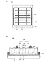
図1(A)に本発明に係る光電変換装置100の上面の模式図を示し、図1(B)に断面の模式図を示す。なお、図1(B)は、図1(A)中のO−P切断線に対応する断面図の一例である。
本形態では、上記実施の形態と異なる光電変換装置の製造方法について説明する。上記実施の形態では、単結晶シリコン基板101から薄片化した第1単結晶シリコン層110にレーザ処理を行うことによって結晶欠陥の修復を行う例について示した。本実施の形態では、第1単結晶シリコン層110表面を除去して結晶欠陥の低減を図る方法に関して説明する。なお、その他の構成は上記実施の形態に準じるものとし、説明は省略する。
本形態では、上記実施の形態と異なる光電変換装置の製造方法について、図10乃至図12を参照して説明する。具体的には、単結晶シリコン基板101に脆化層103、第1不純物シリコン層108、第1電極106及び絶縁層104を形成する方法に関して説明する。なお、その他の構成は上記実施の形態に準じるものとし、説明は省略する。
本形態では、上記実施の形態と異なる構成の光電変換装置について、図13を参照して説明する。具体的には、上記実施の形態では絶縁層104と支持基板102との間で接合する例を示したが、本形態では絶縁層104を設けることなく第1電極106と支持基板102との間で接合する例について説明する。
本形態では、単結晶シリコン層を分離して残る剥離基板130を再生処理する例について説明する。
本形態では、ユニットセルを複数積層した光電変換装置の例について説明する。本形態では、ユニットセルを2層積層した所謂タンデム型の光電変換装置について説明する。
本形態では、ユニットセルを複数積層した光電変換装置、具体的にはユニットセルを3層積層した所謂スタック型の光電変換装置について図面を参照して説明する。
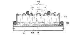
実施形態1乃至7により得られる光電変換装置を用いて太陽光発電モジュールを製造することができる。本実施の形態では、上記実施の形態に示す光電変換装置を用いた太陽光発電モジュールの一例を図20(A)に示す。太陽光発電モジュール1028は、支持基板102の一面上に設けられたユニットセル116により構成されている。支持基板102とユニットセル116との間には、支持基板102側から絶縁層104、第1電極106が設けられている。第1電極106は補助電極118と接続している。
図21は上記実施の形態8で示した太陽光発電モジュール1028を用いた太陽光発電システムの一例を示す。一又は複数の太陽光発電モジュール1028の出力電力は、充電制御回路1029により蓄電池1030を充電する。蓄電池1030の充電量が多い場合には、負荷1031に直接出力される場合もある。
101 単結晶シリコン基板
102 支持基板
103 脆化層
104 絶縁層
105 保護層
106 電極
108 不純物シリコン層
110 単結晶シリコン層
112 単結晶シリコン層
113 単結晶シリコン層
114 不純物シリコン層
116 ユニットセル
118 補助電極
119 パッシベーション層
120 電極
130 剥離基板
180 レーザビーム
Claims (2)
- 単結晶シリコン基板の一表面側からイオン又はクラスターイオンを照射して前記一表面側から所定の深さの領域に脆化層を形成し、且つ前記単結晶シリコン基板の一表面側に第1不純物シリコン層、第1電極および絶縁層を形成し、
ガラス基板の一表面側と、前記単結晶シリコン基板の一表面側と、を対向させ、前記ガラス基板の一表面側と前記絶縁層とを重ね合わせて貼り合わせ、
熱処理を行い、前記脆化層を境として前記単結晶シリコン基板を分離させ、前記ガラス基板上に単結晶シリコン層を40nm以上300nm以下の厚さで形成し、
前記単結晶シリコン層の結晶欠陥修復処理又は結晶欠陥除去処理を行った後、
前記ガラス基板の温度を600℃以上670℃以下にし、シラン系ガスを少なくとも含む原料ガスを用い、大気圧或いは大気圧近傍下で生成したプラズマにより前記原料ガスを活性化させ、前記単結晶シリコン層を1μm以上20μm以下でエピタキシャル成長させ、
前記単結晶シリコン層のエピタキシャル成長させた表面側に第2不純物シリコン層および第2の電極を形成する光電変換装置の製造方法であって、
照射する前記イオン又はクラスターイオンとしては、H3 +イオンの割合を多くすることを特徴とする光電変換装置の製造方法。 - 請求項1において、
大気圧或いは大気圧近傍とは、0.1気圧乃至10気圧の範囲とすることを特徴とする光電変換装置の製造方法。
Priority Applications (1)
Application Number | Priority Date | Filing Date | Title |
---|---|---|---|
JP2008319106A JP5572307B2 (ja) | 2007-12-28 | 2008-12-16 | 光電変換装置の製造方法 |
Applications Claiming Priority (3)
Application Number | Priority Date | Filing Date | Title |
---|---|---|---|
JP2007338578 | 2007-12-28 | ||
JP2008319106A JP5572307B2 (ja) | 2007-12-28 | 2008-12-16 | 光電変換装置の製造方法 |
Publications (3)
Publication Number | Publication Date |
---|---|
JP2009177145A JP2009177145A (ja) | 2009-08-06 |
JP2009177145A5 JP2009177145A5 (ja) | 2012-01-12 |
JP5572307B2 true JP5572307B2 (ja) | 2014-08-13 |
Family
ID=40828639
Family Applications (1)
Application Number | Title | Priority Date | Filing Date |
---|---|---|---|
JP2008319106A Expired - Fee Related JP5572307B2 (ja) | 2007-12-28 | 2008-12-16 | 光電変換装置の製造方法 |
Country Status (4)
Country | Link |
---|---|
US (1) | US8008169B2 (ja) |
JP (1) | JP5572307B2 (ja) |
CN (1) | CN101471398B (ja) |
TW (1) | TWI442590B (ja) |
Families Citing this family (30)
Publication number | Priority date | Publication date | Assignee | Title |
---|---|---|---|---|
US8017429B2 (en) | 2008-02-19 | 2011-09-13 | Semiconductor Energy Laboratory Co., Ltd. | Method for manufacturing photoelectric conversion device |
JP5654206B2 (ja) * | 2008-03-26 | 2015-01-14 | 株式会社半導体エネルギー研究所 | Soi基板の作製方法及び該soi基板を用いた半導体装置 |
TWI416757B (zh) * | 2008-10-13 | 2013-11-21 | Advanced Optoelectronic Tech | 多波長發光二極體及其製造方法 |
US20110041910A1 (en) * | 2009-08-18 | 2011-02-24 | Semiconductor Energy Laboratory Co., Ltd. | Photoelectric conversion device and manufacturing method thereof |
JP5706670B2 (ja) | 2009-11-24 | 2015-04-22 | 株式会社半導体エネルギー研究所 | Soi基板の作製方法 |
FR2955702B1 (fr) * | 2010-01-27 | 2012-01-27 | Commissariat Energie Atomique | Cellule photovoltaique comprenant un film mince de passivation en oxyde cristallin de silicium et procede de realisation |
US8704083B2 (en) | 2010-02-11 | 2014-04-22 | Semiconductor Energy Laboratory Co., Ltd. | Photoelectric conversion device and fabrication method thereof |
JP5726434B2 (ja) | 2010-04-14 | 2015-06-03 | 浜松ホトニクス株式会社 | 半導体光検出素子 |
US8614495B2 (en) * | 2010-04-23 | 2013-12-24 | Taiwan Semiconductor Manufacturing Company, Ltd. | Back side defect reduction for back side illuminated image sensor |
JP5755931B2 (ja) | 2010-04-28 | 2015-07-29 | 株式会社半導体エネルギー研究所 | 半導体膜の作製方法、電極の作製方法、2次電池の作製方法、および太陽電池の作製方法 |
JP5554142B2 (ja) * | 2010-05-14 | 2014-07-23 | 株式会社豊田中央研究所 | 半導体膜の気相成長方法 |
JP5622231B2 (ja) * | 2010-10-06 | 2014-11-12 | 三菱重工業株式会社 | 光電変換装置の製造方法 |
JP5912404B2 (ja) * | 2010-10-29 | 2016-04-27 | 株式会社半導体エネルギー研究所 | 光電変換装置 |
SG188730A1 (en) * | 2011-09-07 | 2013-04-30 | Air Prod & Chem | Precursors for photovoltaic passivation |
KR20130070892A (ko) * | 2011-12-20 | 2013-06-28 | 한국전자통신연구원 | 광 검출기 소자 |
US9099578B2 (en) | 2012-06-04 | 2015-08-04 | Nusola, Inc. | Structure for creating ohmic contact in semiconductor devices and methods for manufacture |
WO2013152054A1 (en) * | 2012-04-02 | 2013-10-10 | Nusola Inc. | Photovoltaic cell and process of manufacture |
US9276164B2 (en) * | 2012-11-26 | 2016-03-01 | Epistar Corporation | Optoelectronic device and method for manufacturing the same |
CN106158988B (zh) * | 2015-04-07 | 2017-12-12 | 昱晶能源科技股份有限公司 | 太阳能电池及其制造方法 |
US9972489B2 (en) | 2015-05-28 | 2018-05-15 | SemiNuclear, Inc. | Composition and method for making picocrystalline artificial borane atoms |
US11651957B2 (en) | 2015-05-28 | 2023-05-16 | SemiNuclear, Inc. | Process and manufacture of low-dimensional materials supporting both self-thermalization and self-localization |
KR101680036B1 (ko) * | 2015-07-07 | 2016-12-12 | 엘지전자 주식회사 | 태양 전지 및 이의 제조 방법 |
US20170012154A1 (en) * | 2015-07-09 | 2017-01-12 | Solaero Technologies Corp. | Method for producing solar cells and solar cell assemblies |
JP6459948B2 (ja) * | 2015-12-15 | 2019-01-30 | 株式会社Sumco | 半導体エピタキシャルウェーハの製造方法および固体撮像素子の製造方法 |
US9735267B1 (en) * | 2016-01-28 | 2017-08-15 | Taiwan Semiconductor Manufacturing Co., Ltd. | Structure and formation method of semiconductor device structure |
JP6259878B1 (ja) * | 2016-08-26 | 2018-01-10 | 株式会社フジクラ | 光電変換素子 |
CN110267915B (zh) * | 2016-11-29 | 2023-04-25 | 半核子有限公司 | 制备皮晶人造硼烷原子的组合物和方法 |
CN107265878A (zh) * | 2017-06-06 | 2017-10-20 | 界首市七曜新能源有限公司 | 高透光率太阳能热水器专用真空管 |
CN111987191A (zh) * | 2020-09-09 | 2020-11-24 | 苏州腾晖光伏技术有限公司 | 一种修复perc电池激光开膜损伤的方法 |
JP7282961B1 (ja) | 2022-07-28 | 2023-05-29 | 株式会社東芝 | 光電変換素子の検査装置、光電変換素子の製造装置、光電変換素子の製造方法 |
Family Cites Families (85)
Publication number | Priority date | Publication date | Assignee | Title |
---|---|---|---|---|
US4180618A (en) | 1977-07-27 | 1979-12-25 | Corning Glass Works | Thin silicon film electronic device |
US5091334A (en) | 1980-03-03 | 1992-02-25 | Semiconductor Energy Laboratory Co., Ltd. | Semiconductor device |
JPS56122123A (en) | 1980-03-03 | 1981-09-25 | Shunpei Yamazaki | Semiamorphous semiconductor |
DE3177084D1 (en) | 1980-04-10 | 1989-09-21 | Massachusetts Inst Technology | Method of producing sheets of crystalline material |
JPS5771126A (en) | 1980-10-21 | 1982-05-01 | Semiconductor Energy Lab Co Ltd | Semiamorhous semiconductor |
JPS5972781A (ja) | 1982-10-20 | 1984-04-24 | Semiconductor Energy Lab Co Ltd | 光電変換半導体装置 |
US4496788A (en) | 1982-12-29 | 1985-01-29 | Osaka Transformer Co., Ltd. | Photovoltaic device |
US4633034A (en) | 1985-02-08 | 1986-12-30 | Energy Conversion Devices, Inc. | Photovoltaic device and method |
ATE217447T1 (de) | 1990-08-03 | 2002-05-15 | Canon Kk | Verfahren zur herstellung eines halbleiterkörpers |
US5750000A (en) | 1990-08-03 | 1998-05-12 | Canon Kabushiki Kaisha | Semiconductor member, and process for preparing same and semiconductor device formed by use of same |
KR950013784B1 (ko) | 1990-11-20 | 1995-11-16 | 가부시키가이샤 한도오따이 에네루기 겐큐쇼 | 반도체 전계효과 트랜지스터 및 그 제조방법과 박막트랜지스터 |
US5849601A (en) | 1990-12-25 | 1998-12-15 | Semiconductor Energy Laboratory Co., Ltd. | Electro-optical device and method for manufacturing the same |
US7115902B1 (en) | 1990-11-20 | 2006-10-03 | Semiconductor Energy Laboratory Co., Ltd. | Electro-optical device and method for manufacturing the same |
US5514879A (en) | 1990-11-20 | 1996-05-07 | Semiconductor Energy Laboratory Co., Ltd. | Gate insulated field effect transistors and method of manufacturing the same |
JP2840699B2 (ja) | 1990-12-12 | 1998-12-24 | 株式会社 半導体エネルギー研究所 | 被膜形成装置及び被膜形成方法 |
US7576360B2 (en) | 1990-12-25 | 2009-08-18 | Semiconductor Energy Laboratory Co., Ltd. | Electro-optical device which comprises thin film transistors and method for manufacturing the same |
US7098479B1 (en) | 1990-12-25 | 2006-08-29 | Semiconductor Energy Laboratory Co., Ltd. | Electro-optical device and method for manufacturing the same |
CA2069038C (en) | 1991-05-22 | 1997-08-12 | Kiyofumi Sakaguchi | Method for preparing semiconductor member |
US5705828A (en) * | 1991-08-10 | 1998-01-06 | Sanyo Electric Co., Ltd. | Photovoltaic device |
US5946587A (en) | 1992-08-06 | 1999-08-31 | Canon Kabushiki Kaisha | Continuous forming method for functional deposited films |
US6835523B1 (en) | 1993-05-09 | 2004-12-28 | Semiconductor Energy Laboratory Co., Ltd. | Apparatus for fabricating coating and method of fabricating the coating |
JP3360919B2 (ja) | 1993-06-11 | 2003-01-07 | 三菱電機株式会社 | 薄膜太陽電池の製造方法,及び薄膜太陽電池 |
US6183816B1 (en) | 1993-07-20 | 2001-02-06 | Semiconductor Energy Laboratory Co., Ltd. | Method of fabricating the coating |
JP3352340B2 (ja) | 1995-10-06 | 2002-12-03 | キヤノン株式会社 | 半導体基体とその製造方法 |
JP3381443B2 (ja) | 1995-02-02 | 2003-02-24 | ソニー株式会社 | 基体から半導体層を分離する方法、半導体素子の製造方法およびsoi基板の製造方法 |
US5736431A (en) | 1995-02-28 | 1998-04-07 | Semiconductor Energy Laboratory Co., Ltd. | Method for producing thin film solar battery |
US5716480A (en) * | 1995-07-13 | 1998-02-10 | Canon Kabushiki Kaisha | Photovoltaic device and method of manufacturing the same |
JPH09255487A (ja) * | 1996-03-18 | 1997-09-30 | Sony Corp | 薄膜半導体の製造方法 |
JPH1093122A (ja) * | 1996-09-10 | 1998-04-10 | Nippon Telegr & Teleph Corp <Ntt> | 薄膜太陽電池の製造方法 |
DE69738307T2 (de) | 1996-12-27 | 2008-10-02 | Canon K.K. | Herstellungsverfahren eines Halbleiter-Bauelements und Herstellungsverfahren einer Solarzelle |
JPH10335683A (ja) | 1997-05-28 | 1998-12-18 | Ion Kogaku Kenkyusho:Kk | タンデム型太陽電池およびその製造方法 |
JP4027465B2 (ja) | 1997-07-01 | 2007-12-26 | 株式会社半導体エネルギー研究所 | アクティブマトリクス型表示装置およびその製造方法 |
US6534380B1 (en) | 1997-07-18 | 2003-03-18 | Denso Corporation | Semiconductor substrate and method of manufacturing the same |
JPH11103082A (ja) | 1997-09-26 | 1999-04-13 | Canon Inc | 光起電力素子及びその作製方法 |
JPH11163363A (ja) | 1997-11-22 | 1999-06-18 | Semiconductor Energy Lab Co Ltd | 半導体装置およびその作製方法 |
US6331208B1 (en) | 1998-05-15 | 2001-12-18 | Canon Kabushiki Kaisha | Process for producing solar cell, process for producing thin-film semiconductor, process for separating thin-film semiconductor, and process for forming semiconductor |
JP2000012864A (ja) | 1998-06-22 | 2000-01-14 | Semiconductor Energy Lab Co Ltd | 半導体装置の作製方法 |
JP2000124092A (ja) | 1998-10-16 | 2000-04-28 | Shin Etsu Handotai Co Ltd | 水素イオン注入剥離法によってsoiウエーハを製造する方法およびこの方法で製造されたsoiウエーハ |
JP2000150940A (ja) | 1998-11-18 | 2000-05-30 | Denso Corp | 半導体微粒子集合体及びその製造方法 |
JP2000349264A (ja) | 1998-12-04 | 2000-12-15 | Canon Inc | 半導体ウエハの製造方法、使用方法および利用方法 |
JP2000277439A (ja) | 1999-03-25 | 2000-10-06 | Kanegafuchi Chem Ind Co Ltd | 結晶質シリコン系薄膜のプラズマcvd方法およびシリコン系薄膜光電変換装置の製造方法 |
JP2000349266A (ja) * | 1999-03-26 | 2000-12-15 | Canon Inc | 半導体部材の製造方法、半導体基体の利用方法、半導体部材の製造システム、半導体部材の生産管理方法及び堆積膜形成装置の利用方法 |
JP2001015721A (ja) | 1999-04-30 | 2001-01-19 | Canon Inc | 複合部材の分離方法及び薄膜の製造方法 |
TW477009B (en) | 1999-05-26 | 2002-02-21 | Tadahiro Ohmi | Plasma process device |
US6387829B1 (en) | 1999-06-18 | 2002-05-14 | Silicon Wafer Technologies, Inc. | Separation process for silicon-on-insulator wafer fabrication |
JP2001089291A (ja) * | 1999-09-20 | 2001-04-03 | Canon Inc | 液相成長法、半導体部材の製造方法、太陽電池の製造方法 |
JP2001160540A (ja) | 1999-09-22 | 2001-06-12 | Canon Inc | 半導体装置の製造方法、液相成長法及び液相成長装置、太陽電池 |
JP3513592B2 (ja) | 2000-09-25 | 2004-03-31 | 独立行政法人産業技術総合研究所 | 太陽電池の製造方法 |
JP3480448B2 (ja) | 2001-03-05 | 2003-12-22 | 森 勇蔵 | エピタキシャルSiの高速成膜方法 |
JP2002348198A (ja) | 2001-05-28 | 2002-12-04 | Nissin Electric Co Ltd | 半導体素子エピタキシャル成長用基板及びその製造方法 |
JP2002371357A (ja) | 2001-06-14 | 2002-12-26 | Canon Inc | シリコン系薄膜の形成方法、シリコン系薄膜及び半導体素子並びにシリコン系薄膜の形成装置 |
TW521540B (en) | 2001-10-03 | 2003-02-21 | Hau-Ran Ni | An ECR plasma reactor system with multiple exciters |
JP3902534B2 (ja) * | 2001-11-29 | 2007-04-11 | 三洋電機株式会社 | 光起電力装置及びその製造方法 |
KR100442105B1 (ko) * | 2001-12-03 | 2004-07-27 | 삼성전자주식회사 | 소이형 기판 형성 방법 |
JP4070483B2 (ja) * | 2002-03-05 | 2008-04-02 | 三洋電機株式会社 | 光起電力装置並びにその製造方法 |
JP2004014958A (ja) | 2002-06-11 | 2004-01-15 | Fuji Electric Holdings Co Ltd | 薄膜多結晶太陽電池とその製造方法 |
US6818529B2 (en) | 2002-09-12 | 2004-11-16 | Applied Materials, Inc. | Apparatus and method for forming a silicon film across the surface of a glass substrate |
JP2004265889A (ja) * | 2003-01-16 | 2004-09-24 | Tdk Corp | 光電変換素子、光電変換装置、及び鉄シリサイド膜 |
JP4907088B2 (ja) | 2003-02-05 | 2012-03-28 | 株式会社半導体エネルギー研究所 | 表示装置の製造方法 |
JP4748954B2 (ja) | 2003-07-14 | 2011-08-17 | 株式会社半導体エネルギー研究所 | 液晶表示装置 |
TWI336921B (en) | 2003-07-18 | 2011-02-01 | Semiconductor Energy Lab | Method for manufacturing semiconductor device |
JP4480968B2 (ja) | 2003-07-18 | 2010-06-16 | 株式会社半導体エネルギー研究所 | 表示装置 |
US7211454B2 (en) | 2003-07-25 | 2007-05-01 | Semiconductor Energy Laboratory Co., Ltd. | Manufacturing method of a light emitting device including moving the source of the vapor deposition parallel to the substrate |
JP2005050905A (ja) | 2003-07-30 | 2005-02-24 | Sharp Corp | シリコン薄膜太陽電池の製造方法 |
US7253391B2 (en) | 2003-09-19 | 2007-08-07 | Semiconductor Energy Laboratory Co., Ltd. | Optical sensor device and electronic apparatus |
WO2005047968A1 (en) | 2003-11-14 | 2005-05-26 | Semiconductor Energy Laboratory Co., Ltd. | Display device and method for manufacturing the same |
JP2005268682A (ja) | 2004-03-22 | 2005-09-29 | Canon Inc | 半導体基材及び太陽電池の製造方法 |
JP5013393B2 (ja) | 2005-03-30 | 2012-08-29 | 東京エレクトロン株式会社 | プラズマ処理装置と方法 |
JP2006294422A (ja) | 2005-04-11 | 2006-10-26 | Tokyo Electron Ltd | プラズマ処理装置およびスロットアンテナおよびプラズマ処理方法 |
TWI408734B (zh) | 2005-04-28 | 2013-09-11 | Semiconductor Energy Lab | 半導體裝置及其製造方法 |
JP4597792B2 (ja) | 2005-06-27 | 2010-12-15 | 東京エレクトロン株式会社 | 処理ガス供給構造およびプラズマ処理装置 |
JP4777717B2 (ja) | 2005-08-10 | 2011-09-21 | 東京エレクトロン株式会社 | 成膜方法、プラズマ処理装置および記録媒体 |
US7301215B2 (en) | 2005-08-22 | 2007-11-27 | Canon Kabushiki Kaisha | Photovoltaic device |
EP1950813A4 (en) * | 2005-11-17 | 2010-07-21 | Asahi Glass Co Ltd | TRANSPARENT CONDUCTIVE SUBSTRATE FOR SOLAR CELL AND METHOD FOR MANUFACTURING THE SAME |
JP5068458B2 (ja) | 2006-01-18 | 2012-11-07 | 東京エレクトロン株式会社 | プラズマ処理装置およびプラズマ処理方法 |
JP4978985B2 (ja) | 2006-03-30 | 2012-07-18 | 東京エレクトロン株式会社 | プラズマ処理方法 |
EP2002484A4 (en) | 2006-04-05 | 2016-06-08 | Silicon Genesis Corp | METHOD AND STRUCTURE FOR MANUFACTURING PHOTOVOLTAIC CELLS USING A LAYER TRANSFER PROCESS |
JP2008112847A (ja) | 2006-10-30 | 2008-05-15 | Shin Etsu Chem Co Ltd | 単結晶シリコン太陽電池の製造方法及び単結晶シリコン太陽電池 |
EP2135295A4 (en) | 2007-04-06 | 2014-05-21 | Semiconductor Energy Lab | Photovoltaic module and method for its production |
JP5364293B2 (ja) | 2007-06-01 | 2013-12-11 | 株式会社半導体エネルギー研究所 | 表示装置の作製方法およびプラズマcvd装置 |
US8207010B2 (en) | 2007-06-05 | 2012-06-26 | Semiconductor Energy Laboratory Co., Ltd. | Method for manufacturing photoelectric conversion device |
JP5058084B2 (ja) | 2007-07-27 | 2012-10-24 | 株式会社半導体エネルギー研究所 | 光電変換装置の作製方法及びマイクロ波プラズマcvd装置 |
JP5216446B2 (ja) | 2007-07-27 | 2013-06-19 | 株式会社半導体エネルギー研究所 | プラズマcvd装置及び表示装置の作製方法 |
JP5248994B2 (ja) | 2007-11-30 | 2013-07-31 | 株式会社半導体エネルギー研究所 | 光電変換装置の製造方法 |
JP5248995B2 (ja) | 2007-11-30 | 2013-07-31 | 株式会社半導体エネルギー研究所 | 光電変換装置の製造方法 |
-
2008
- 2008-12-16 JP JP2008319106A patent/JP5572307B2/ja not_active Expired - Fee Related
- 2008-12-22 US US12/341,699 patent/US8008169B2/en not_active Expired - Fee Related
- 2008-12-22 TW TW097150079A patent/TWI442590B/zh not_active IP Right Cessation
- 2008-12-29 CN CN200810189178XA patent/CN101471398B/zh not_active Expired - Fee Related
Also Published As
Publication number | Publication date |
---|---|
US8008169B2 (en) | 2011-08-30 |
US20100047952A1 (en) | 2010-02-25 |
TWI442590B (zh) | 2014-06-21 |
TW200945613A (en) | 2009-11-01 |
CN101471398A (zh) | 2009-07-01 |
JP2009177145A (ja) | 2009-08-06 |
CN101471398B (zh) | 2012-11-14 |
Similar Documents
Publication | Publication Date | Title |
---|---|---|
JP5572307B2 (ja) | 光電変換装置の製造方法 | |
JP5248995B2 (ja) | 光電変換装置の製造方法 | |
JP5248994B2 (ja) | 光電変換装置の製造方法 | |
JP5459901B2 (ja) | 光電変換装置モジュールの作製方法 | |
JP5352190B2 (ja) | 光電変換装置 | |
JP5286046B2 (ja) | 光電変換装置の製造方法 | |
JP5469889B2 (ja) | 光電変換装置の製造方法 | |
JP5286146B2 (ja) | 光電変換装置の作製方法 | |
TWI557928B (zh) | 光電轉換裝置及其製造方法 | |
JP5438986B2 (ja) | 光電変換装置の製造方法 | |
JP5315008B2 (ja) | 光電変換装置 | |
US20110041910A1 (en) | Photoelectric conversion device and manufacturing method thereof |
Legal Events
Date | Code | Title | Description |
---|---|---|---|
RD02 | Notification of acceptance of power of attorney |
Free format text: JAPANESE INTERMEDIATE CODE: A7422 Effective date: 20111017 |
|
A521 | Request for written amendment filed |
Free format text: JAPANESE INTERMEDIATE CODE: A523 Effective date: 20111117 |
|
A621 | Written request for application examination |
Free format text: JAPANESE INTERMEDIATE CODE: A621 Effective date: 20111117 |
|
A977 | Report on retrieval |
Free format text: JAPANESE INTERMEDIATE CODE: A971007 Effective date: 20121010 |
|
A131 | Notification of reasons for refusal |
Free format text: JAPANESE INTERMEDIATE CODE: A131 Effective date: 20121016 |
|
A521 | Request for written amendment filed |
Free format text: JAPANESE INTERMEDIATE CODE: A523 Effective date: 20121106 |
|
A02 | Decision of refusal |
Free format text: JAPANESE INTERMEDIATE CODE: A02 Effective date: 20130618 |
|
A521 | Request for written amendment filed |
Free format text: JAPANESE INTERMEDIATE CODE: A523 Effective date: 20130809 |
|
A911 | Transfer to examiner for re-examination before appeal (zenchi) |
Free format text: JAPANESE INTERMEDIATE CODE: A911 Effective date: 20130820 |
|
A912 | Re-examination (zenchi) completed and case transferred to appeal board |
Free format text: JAPANESE INTERMEDIATE CODE: A912 Effective date: 20131025 |
|
A521 | Request for written amendment filed |
Free format text: JAPANESE INTERMEDIATE CODE: A523 Effective date: 20140512 |
|
A521 | Request for written amendment filed |
Free format text: JAPANESE INTERMEDIATE CODE: A523 Effective date: 20140526 |
|
A61 | First payment of annual fees (during grant procedure) |
Free format text: JAPANESE INTERMEDIATE CODE: A61 Effective date: 20140630 |
|
R150 | Certificate of patent or registration of utility model |
Ref document number: 5572307 Country of ref document: JP Free format text: JAPANESE INTERMEDIATE CODE: R150 |
|
R250 | Receipt of annual fees |
Free format text: JAPANESE INTERMEDIATE CODE: R250 |
|
LAPS | Cancellation because of no payment of annual fees |