US11651957B2 - Process and manufacture of low-dimensional materials supporting both self-thermalization and self-localization - Google Patents
Process and manufacture of low-dimensional materials supporting both self-thermalization and self-localization Download PDFInfo
- Publication number
- US11651957B2 US11651957B2 US16/425,582 US201916425582A US11651957B2 US 11651957 B2 US11651957 B2 US 11651957B2 US 201916425582 A US201916425582 A US 201916425582A US 11651957 B2 US11651957 B2 US 11651957B2
- Authority
- US
- United States
- Prior art keywords
- layer
- boron
- phonovoltaic
- oxysilaborane
- picocrystalline
- Prior art date
- Legal status (The legal status is an assumption and is not a legal conclusion. Google has not performed a legal analysis and makes no representation as to the accuracy of the status listed.)
- Active, expires
Links
Images


Classifications
-
- C—CHEMISTRY; METALLURGY
- C07—ORGANIC CHEMISTRY
- C07F—ACYCLIC, CARBOCYCLIC OR HETEROCYCLIC COMPOUNDS CONTAINING ELEMENTS OTHER THAN CARBON, HYDROGEN, HALOGEN, OXYGEN, NITROGEN, SULFUR, SELENIUM OR TELLURIUM
- C07F7/00—Compounds containing elements of Groups 4 or 14 of the Periodic System
- C07F7/02—Silicon compounds
- C07F7/21—Cyclic compounds having at least one ring containing silicon, but no carbon in the ring
-
- C—CHEMISTRY; METALLURGY
- C23—COATING METALLIC MATERIAL; COATING MATERIAL WITH METALLIC MATERIAL; CHEMICAL SURFACE TREATMENT; DIFFUSION TREATMENT OF METALLIC MATERIAL; COATING BY VACUUM EVAPORATION, BY SPUTTERING, BY ION IMPLANTATION OR BY CHEMICAL VAPOUR DEPOSITION, IN GENERAL; INHIBITING CORROSION OF METALLIC MATERIAL OR INCRUSTATION IN GENERAL
- C23C—COATING METALLIC MATERIAL; COATING MATERIAL WITH METALLIC MATERIAL; SURFACE TREATMENT OF METALLIC MATERIAL BY DIFFUSION INTO THE SURFACE, BY CHEMICAL CONVERSION OR SUBSTITUTION; COATING BY VACUUM EVAPORATION, BY SPUTTERING, BY ION IMPLANTATION OR BY CHEMICAL VAPOUR DEPOSITION, IN GENERAL
- C23C16/00—Chemical coating by decomposition of gaseous compounds, without leaving reaction products of surface material in the coating, i.e. chemical vapour deposition [CVD] processes
- C23C16/22—Chemical coating by decomposition of gaseous compounds, without leaving reaction products of surface material in the coating, i.e. chemical vapour deposition [CVD] processes characterised by the deposition of inorganic material, other than metallic material
- C23C16/30—Deposition of compounds, mixtures or solid solutions, e.g. borides, carbides, nitrides
- C23C16/38—Borides
-
- C—CHEMISTRY; METALLURGY
- C23—COATING METALLIC MATERIAL; COATING MATERIAL WITH METALLIC MATERIAL; CHEMICAL SURFACE TREATMENT; DIFFUSION TREATMENT OF METALLIC MATERIAL; COATING BY VACUUM EVAPORATION, BY SPUTTERING, BY ION IMPLANTATION OR BY CHEMICAL VAPOUR DEPOSITION, IN GENERAL; INHIBITING CORROSION OF METALLIC MATERIAL OR INCRUSTATION IN GENERAL
- C23C—COATING METALLIC MATERIAL; COATING MATERIAL WITH METALLIC MATERIAL; SURFACE TREATMENT OF METALLIC MATERIAL BY DIFFUSION INTO THE SURFACE, BY CHEMICAL CONVERSION OR SUBSTITUTION; COATING BY VACUUM EVAPORATION, BY SPUTTERING, BY ION IMPLANTATION OR BY CHEMICAL VAPOUR DEPOSITION, IN GENERAL
- C23C16/00—Chemical coating by decomposition of gaseous compounds, without leaving reaction products of surface material in the coating, i.e. chemical vapour deposition [CVD] processes
- C23C16/22—Chemical coating by decomposition of gaseous compounds, without leaving reaction products of surface material in the coating, i.e. chemical vapour deposition [CVD] processes characterised by the deposition of inorganic material, other than metallic material
- C23C16/30—Deposition of compounds, mixtures or solid solutions, e.g. borides, carbides, nitrides
- C23C16/40—Oxides
- C23C16/401—Oxides containing silicon
-
- C—CHEMISTRY; METALLURGY
- C30—CRYSTAL GROWTH
- C30B—SINGLE-CRYSTAL GROWTH; UNIDIRECTIONAL SOLIDIFICATION OF EUTECTIC MATERIAL OR UNIDIRECTIONAL DEMIXING OF EUTECTOID MATERIAL; REFINING BY ZONE-MELTING OF MATERIAL; PRODUCTION OF A HOMOGENEOUS POLYCRYSTALLINE MATERIAL WITH DEFINED STRUCTURE; SINGLE CRYSTALS OR HOMOGENEOUS POLYCRYSTALLINE MATERIAL WITH DEFINED STRUCTURE; AFTER-TREATMENT OF SINGLE CRYSTALS OR A HOMOGENEOUS POLYCRYSTALLINE MATERIAL WITH DEFINED STRUCTURE; APPARATUS THEREFOR
- C30B25/00—Single-crystal growth by chemical reaction of reactive gases, e.g. chemical vapour-deposition growth
-
- C—CHEMISTRY; METALLURGY
- C30—CRYSTAL GROWTH
- C30B—SINGLE-CRYSTAL GROWTH; UNIDIRECTIONAL SOLIDIFICATION OF EUTECTIC MATERIAL OR UNIDIRECTIONAL DEMIXING OF EUTECTOID MATERIAL; REFINING BY ZONE-MELTING OF MATERIAL; PRODUCTION OF A HOMOGENEOUS POLYCRYSTALLINE MATERIAL WITH DEFINED STRUCTURE; SINGLE CRYSTALS OR HOMOGENEOUS POLYCRYSTALLINE MATERIAL WITH DEFINED STRUCTURE; AFTER-TREATMENT OF SINGLE CRYSTALS OR A HOMOGENEOUS POLYCRYSTALLINE MATERIAL WITH DEFINED STRUCTURE; APPARATUS THEREFOR
- C30B29/00—Single crystals or homogeneous polycrystalline material with defined structure characterised by the material or by their shape
- C30B29/10—Inorganic compounds or compositions
- C30B29/40—AIIIBV compounds wherein A is B, Al, Ga, In or Tl and B is N, P, As, Sb or Bi
- C30B29/403—AIII-nitrides
- C30B29/406—Gallium nitride
-
- C—CHEMISTRY; METALLURGY
- C30—CRYSTAL GROWTH
- C30B—SINGLE-CRYSTAL GROWTH; UNIDIRECTIONAL SOLIDIFICATION OF EUTECTIC MATERIAL OR UNIDIRECTIONAL DEMIXING OF EUTECTOID MATERIAL; REFINING BY ZONE-MELTING OF MATERIAL; PRODUCTION OF A HOMOGENEOUS POLYCRYSTALLINE MATERIAL WITH DEFINED STRUCTURE; SINGLE CRYSTALS OR HOMOGENEOUS POLYCRYSTALLINE MATERIAL WITH DEFINED STRUCTURE; AFTER-TREATMENT OF SINGLE CRYSTALS OR A HOMOGENEOUS POLYCRYSTALLINE MATERIAL WITH DEFINED STRUCTURE; APPARATUS THEREFOR
- C30B7/00—Single-crystal growth from solutions using solvents which are liquid at normal temperature, e.g. aqueous solutions
- C30B7/10—Single-crystal growth from solutions using solvents which are liquid at normal temperature, e.g. aqueous solutions by application of pressure, e.g. hydrothermal processes
- C30B7/105—Single-crystal growth from solutions using solvents which are liquid at normal temperature, e.g. aqueous solutions by application of pressure, e.g. hydrothermal processes using ammonia as solvent, i.e. ammonothermal processes
-
- H—ELECTRICITY
- H01—ELECTRIC ELEMENTS
- H01B—CABLES; CONDUCTORS; INSULATORS; SELECTION OF MATERIALS FOR THEIR CONDUCTIVE, INSULATING OR DIELECTRIC PROPERTIES
- H01B1/00—Conductors or conductive bodies characterised by the conductive materials; Selection of materials as conductors
- H01B1/06—Conductors or conductive bodies characterised by the conductive materials; Selection of materials as conductors mainly consisting of other non-metallic substances
-
- H—ELECTRICITY
- H01—ELECTRIC ELEMENTS
- H01L—SEMICONDUCTOR DEVICES NOT COVERED BY CLASS H10
- H01L21/00—Processes or apparatus adapted for the manufacture or treatment of semiconductor or solid state devices or of parts thereof
- H01L21/02—Manufacture or treatment of semiconductor devices or of parts thereof
- H01L21/02104—Forming layers
- H01L21/02107—Forming insulating materials on a substrate
- H01L21/02109—Forming insulating materials on a substrate characterised by the type of layer, e.g. type of material, porous/non-porous, pre-cursors, mixtures or laminates
- H01L21/02112—Forming insulating materials on a substrate characterised by the type of layer, e.g. type of material, porous/non-porous, pre-cursors, mixtures or laminates characterised by the material of the layer
- H01L21/02123—Forming insulating materials on a substrate characterised by the type of layer, e.g. type of material, porous/non-porous, pre-cursors, mixtures or laminates characterised by the material of the layer the material containing silicon
- H01L21/02126—Forming insulating materials on a substrate characterised by the type of layer, e.g. type of material, porous/non-porous, pre-cursors, mixtures or laminates characterised by the material of the layer the material containing silicon the material containing Si, O, and at least one of H, N, C, F, or other non-metal elements, e.g. SiOC, SiOC:H or SiONC
- H01L21/02129—Forming insulating materials on a substrate characterised by the type of layer, e.g. type of material, porous/non-porous, pre-cursors, mixtures or laminates characterised by the material of the layer the material containing silicon the material containing Si, O, and at least one of H, N, C, F, or other non-metal elements, e.g. SiOC, SiOC:H or SiONC the material being boron or phosphorus doped silicon oxides, e.g. BPSG, BSG or PSG
-
- H—ELECTRICITY
- H01—ELECTRIC ELEMENTS
- H01L—SEMICONDUCTOR DEVICES NOT COVERED BY CLASS H10
- H01L21/00—Processes or apparatus adapted for the manufacture or treatment of semiconductor or solid state devices or of parts thereof
- H01L21/02—Manufacture or treatment of semiconductor devices or of parts thereof
- H01L21/02104—Forming layers
- H01L21/02107—Forming insulating materials on a substrate
- H01L21/02109—Forming insulating materials on a substrate characterised by the type of layer, e.g. type of material, porous/non-porous, pre-cursors, mixtures or laminates
- H01L21/02205—Forming insulating materials on a substrate characterised by the type of layer, e.g. type of material, porous/non-porous, pre-cursors, mixtures or laminates the layer being characterised by the precursor material for deposition
- H01L21/02208—Forming insulating materials on a substrate characterised by the type of layer, e.g. type of material, porous/non-porous, pre-cursors, mixtures or laminates the layer being characterised by the precursor material for deposition the precursor containing a compound comprising Si
-
- H—ELECTRICITY
- H01—ELECTRIC ELEMENTS
- H01L—SEMICONDUCTOR DEVICES NOT COVERED BY CLASS H10
- H01L21/00—Processes or apparatus adapted for the manufacture or treatment of semiconductor or solid state devices or of parts thereof
- H01L21/02—Manufacture or treatment of semiconductor devices or of parts thereof
- H01L21/02104—Forming layers
- H01L21/02107—Forming insulating materials on a substrate
- H01L21/02225—Forming insulating materials on a substrate characterised by the process for the formation of the insulating layer
- H01L21/0226—Forming insulating materials on a substrate characterised by the process for the formation of the insulating layer formation by a deposition process
- H01L21/02263—Forming insulating materials on a substrate characterised by the process for the formation of the insulating layer formation by a deposition process deposition from the gas or vapour phase
- H01L21/02271—Forming insulating materials on a substrate characterised by the process for the formation of the insulating layer formation by a deposition process deposition from the gas or vapour phase deposition by decomposition or reaction of gaseous or vapour phase compounds, i.e. chemical vapour deposition
-
- H—ELECTRICITY
- H01—ELECTRIC ELEMENTS
- H01L—SEMICONDUCTOR DEVICES NOT COVERED BY CLASS H10
- H01L21/00—Processes or apparatus adapted for the manufacture or treatment of semiconductor or solid state devices or of parts thereof
- H01L21/02—Manufacture or treatment of semiconductor devices or of parts thereof
- H01L21/02104—Forming layers
- H01L21/02365—Forming inorganic semiconducting materials on a substrate
- H01L21/02367—Substrates
- H01L21/0237—Materials
- H01L21/02373—Group 14 semiconducting materials
- H01L21/02381—Silicon, silicon germanium, germanium
-
- H—ELECTRICITY
- H01—ELECTRIC ELEMENTS
- H01L—SEMICONDUCTOR DEVICES NOT COVERED BY CLASS H10
- H01L21/00—Processes or apparatus adapted for the manufacture or treatment of semiconductor or solid state devices or of parts thereof
- H01L21/02—Manufacture or treatment of semiconductor devices or of parts thereof
- H01L21/02104—Forming layers
- H01L21/02365—Forming inorganic semiconducting materials on a substrate
- H01L21/02436—Intermediate layers between substrates and deposited layers
- H01L21/02439—Materials
- H01L21/02441—Group 14 semiconducting materials
- H01L21/0245—Silicon, silicon germanium, germanium
-
- H—ELECTRICITY
- H01—ELECTRIC ELEMENTS
- H01L—SEMICONDUCTOR DEVICES NOT COVERED BY CLASS H10
- H01L21/00—Processes or apparatus adapted for the manufacture or treatment of semiconductor or solid state devices or of parts thereof
- H01L21/02—Manufacture or treatment of semiconductor devices or of parts thereof
- H01L21/02104—Forming layers
- H01L21/02365—Forming inorganic semiconducting materials on a substrate
- H01L21/02436—Intermediate layers between substrates and deposited layers
- H01L21/02439—Materials
- H01L21/02488—Insulating materials
-
- H—ELECTRICITY
- H01—ELECTRIC ELEMENTS
- H01L—SEMICONDUCTOR DEVICES NOT COVERED BY CLASS H10
- H01L21/00—Processes or apparatus adapted for the manufacture or treatment of semiconductor or solid state devices or of parts thereof
- H01L21/02—Manufacture or treatment of semiconductor devices or of parts thereof
- H01L21/02104—Forming layers
- H01L21/02365—Forming inorganic semiconducting materials on a substrate
- H01L21/02436—Intermediate layers between substrates and deposited layers
- H01L21/02439—Materials
- H01L21/02491—Conductive materials
-
- H—ELECTRICITY
- H01—ELECTRIC ELEMENTS
- H01L—SEMICONDUCTOR DEVICES NOT COVERED BY CLASS H10
- H01L21/00—Processes or apparatus adapted for the manufacture or treatment of semiconductor or solid state devices or of parts thereof
- H01L21/02—Manufacture or treatment of semiconductor devices or of parts thereof
- H01L21/02104—Forming layers
- H01L21/02365—Forming inorganic semiconducting materials on a substrate
- H01L21/02436—Intermediate layers between substrates and deposited layers
- H01L21/02494—Structure
- H01L21/02496—Layer structure
- H01L21/02505—Layer structure consisting of more than two layers
-
- H—ELECTRICITY
- H01—ELECTRIC ELEMENTS
- H01L—SEMICONDUCTOR DEVICES NOT COVERED BY CLASS H10
- H01L21/00—Processes or apparatus adapted for the manufacture or treatment of semiconductor or solid state devices or of parts thereof
- H01L21/02—Manufacture or treatment of semiconductor devices or of parts thereof
- H01L21/02104—Forming layers
- H01L21/02365—Forming inorganic semiconducting materials on a substrate
- H01L21/02518—Deposited layers
- H01L21/02521—Materials
- H01L21/02565—Oxide semiconducting materials not being Group 12/16 materials, e.g. ternary compounds
-
- H—ELECTRICITY
- H01—ELECTRIC ELEMENTS
- H01L—SEMICONDUCTOR DEVICES NOT COVERED BY CLASS H10
- H01L21/00—Processes or apparatus adapted for the manufacture or treatment of semiconductor or solid state devices or of parts thereof
- H01L21/02—Manufacture or treatment of semiconductor devices or of parts thereof
- H01L21/02104—Forming layers
- H01L21/02365—Forming inorganic semiconducting materials on a substrate
- H01L21/02518—Deposited layers
- H01L21/0257—Doping during depositing
- H01L21/02573—Conductivity type
- H01L21/02579—P-type
-
- H—ELECTRICITY
- H01—ELECTRIC ELEMENTS
- H01L—SEMICONDUCTOR DEVICES NOT COVERED BY CLASS H10
- H01L21/00—Processes or apparatus adapted for the manufacture or treatment of semiconductor or solid state devices or of parts thereof
- H01L21/02—Manufacture or treatment of semiconductor devices or of parts thereof
- H01L21/02104—Forming layers
- H01L21/02365—Forming inorganic semiconducting materials on a substrate
- H01L21/02518—Deposited layers
- H01L21/0257—Doping during depositing
- H01L21/02573—Conductivity type
- H01L21/02581—Transition metal or rare earth elements
-
- H—ELECTRICITY
- H01—ELECTRIC ELEMENTS
- H01L—SEMICONDUCTOR DEVICES NOT COVERED BY CLASS H10
- H01L21/00—Processes or apparatus adapted for the manufacture or treatment of semiconductor or solid state devices or of parts thereof
- H01L21/02—Manufacture or treatment of semiconductor devices or of parts thereof
- H01L21/02104—Forming layers
- H01L21/02365—Forming inorganic semiconducting materials on a substrate
- H01L21/02518—Deposited layers
- H01L21/02587—Structure
- H01L21/0259—Microstructure
- H01L21/02595—Microstructure polycrystalline
-
- H—ELECTRICITY
- H01—ELECTRIC ELEMENTS
- H01L—SEMICONDUCTOR DEVICES NOT COVERED BY CLASS H10
- H01L21/00—Processes or apparatus adapted for the manufacture or treatment of semiconductor or solid state devices or of parts thereof
- H01L21/02—Manufacture or treatment of semiconductor devices or of parts thereof
- H01L21/02104—Forming layers
- H01L21/02365—Forming inorganic semiconducting materials on a substrate
- H01L21/02612—Formation types
- H01L21/02617—Deposition types
- H01L21/0262—Reduction or decomposition of gaseous compounds, e.g. CVD
-
- H—ELECTRICITY
- H01—ELECTRIC ELEMENTS
- H01L—SEMICONDUCTOR DEVICES NOT COVERED BY CLASS H10
- H01L21/00—Processes or apparatus adapted for the manufacture or treatment of semiconductor or solid state devices or of parts thereof
- H01L21/02—Manufacture or treatment of semiconductor devices or of parts thereof
- H01L21/02104—Forming layers
- H01L21/02365—Forming inorganic semiconducting materials on a substrate
- H01L21/02518—Deposited layers
- H01L21/02521—Materials
-
- H—ELECTRICITY
- H10—SEMICONDUCTOR DEVICES; ELECTRIC SOLID-STATE DEVICES NOT OTHERWISE PROVIDED FOR
- H10N—ELECTRIC SOLID-STATE DEVICES NOT OTHERWISE PROVIDED FOR
- H10N10/00—Thermoelectric devices comprising a junction of dissimilar materials, i.e. devices exhibiting Seebeck or Peltier effects
-
- H—ELECTRICITY
- H10—SEMICONDUCTOR DEVICES; ELECTRIC SOLID-STATE DEVICES NOT OTHERWISE PROVIDED FOR
- H10N—ELECTRIC SOLID-STATE DEVICES NOT OTHERWISE PROVIDED FOR
- H10N60/00—Superconducting devices
- H10N60/80—Constructional details
- H10N60/85—Superconducting active materials
-
- H—ELECTRICITY
- H10—SEMICONDUCTOR DEVICES; ELECTRIC SOLID-STATE DEVICES NOT OTHERWISE PROVIDED FOR
- H10N—ELECTRIC SOLID-STATE DEVICES NOT OTHERWISE PROVIDED FOR
- H10N60/00—Superconducting devices
- H10N60/99—Alleged superconductivity
Definitions
- This invention relates to low-dimensional materials and, specifically, to low-dimensional materials which support a quantum self-thermalization and a quantum self-localization, as well as the quantum phase transition between said quantum phases, by means of a controlled variation in the quantum entanglement of carbon-like artificial nuclei in tetravalent artificial atoms that self-assemble.
- thermodynamic cycle in 1824 that can describe a reversible thermomechanical heat engine operating between two heat reservoirs of different temperatures.
- Said thermodynamic cycle is known as the Carnot cycle.
- Any system undergoing the Carnot cycle is referred to as a Carnot heat engine.
- the laws of thermodynamics evolved from numerous investigations into the Carnot cycle. In the development of his namesake thermodynamic cycle, Carnot employed the caloric theory of heat.
- Clausius (1851) The Carnot cycle represented by Clausius (1851) is shown in FIG. 1 with a somewhat different symbolic representation.
- the Carnot cycle in FIG. 1 comprises four infinitesimal variations in the working substance: (1) isothermal expansion A ⁇ B; (2) adiabatic expansion B ⁇ C; (3) isothermal compression C ⁇ D; and (4) adiabatic compression D ⁇ A.
- isothermal expansion A ⁇ B the working substance is expanded at a constant temperature T by the extraction of latent heat Q A ⁇ B from the high-temperature T heat reservoir.
- adiabatic expansion B ⁇ C the working substance is adiabatically cooled from T to T ⁇ dT without an external heat exchange.
- a Carnot heat engine operating in accordance with the Carnot cycle in FIG. 1 constitutes a thermomechanical motor in which the difference between a larger latent heat Q A ⁇ B extracted from the high-temperature T heat reservoir and a lesser latent heat ⁇ Q C ⁇ D thereafter discharged into a low-temperature T ⁇ dT heat reservoir is converted into mechanical work.
- the change in entropy ⁇ S is generally given by:
- the Carnot cycle is reversible, such that the Carnot heat engine can operate either as a motor or a refrigerator. Under such a condition, the equality holds in Eq. (1) such that entropy is therefore conserved in the Carnot cycle.
- the Carnot cycle in FIG. 1 can also be represented in the manner portrayed in FIG. 2 , wherein the intensive thermodynamic variable along the ordinate is temperature T and the extensive thermodynamic variable along the abscissa is entropy S.
- the conservation of entropy in the Carnot cycle is deceptive in that the capability to perform work upon demand requires a spontaneity due to an irreversible process. In the case of a Carnot heat engine operating as a motor, the required spontaneity is associated with the generation of the high-temperature heat reservoir. During the Industrial Revolution, combustion was taken as a given in the Carnot cycle.
- Combustion is a chemical reaction in thermomechanical equilibrium with its surroundings which progresses in the direction of a decrease in Gibbs free energy ⁇ G ⁇ 0 which, in turn, progresses in the direction of a decrease in enthalpy ⁇ H ⁇ 0 and/or an increase in entropy ⁇ S>0 per the following reaction.
- ⁇ G ⁇ H ⁇ T ⁇ S ⁇ 0 (2)
- thermodynamics For chemical reactions ideally in thermomechanical equilibrium with the surroundings, the second law of thermodynamics can be expressed by:
- thermodynamics manifests an increase in entropy in any energy transformation progressing upon its own accord.
- the spontaneity of most fuels is due to a decrease in enthalpy, such that Eq. (3) is more specifically:
- the total entropy of both the working substance and its surroundings ⁇ G/T increases due to a decrease in the Gibbs free energy ⁇ G ⁇ 0 as a result of the formation of molecular bonding orbitals with a greater bound energy.
- the fuel-based economy of the world increases the entropy of the biosphere, depletes the natural fuels, and discharges harmful waste products into the biosphere due to the dependence on high-enthalpy fuels.
- Kirchhoff (1860) stated his law of radiation as: “The ratio between the emissive and absorptive power is the same for all bodies at the same temperature.” Kirchhoff's radiation law can be expressed in terms of a spectral radiance K(v,T).
- Planck (1901) thereby invoked a probabilistic interpretation of a Planckian resonator in his paper: “We now set the entropy S N of the system proportional to the logarithm of its probability W, within an arbitrary additive constant, so that the N resonators together have the energy E N .”
- S N k log W +constant (8)
- Planck (1901) derived the entropy S of each Planckian resonator as:
- Planck (1901) established that the radiative energy density u(v,T)dv within each spectral frequency interval v to v+dv satisfies the following relation.
- Planck statistically obtained the resonator entropy S and resonator energy U only Planck's spectral energy density u(v,T) can be experimentally measured.
- the blackbody radiation introduced by Kirchhoff (1860) was experimentally evaluated by the cavity radiation inside a hollow cavity formed by some insulating enclosure with walls in thermal equilibrium. The heat radiation within said cavity is allowed to achieve radiative equilibrium such that the rates of radiation emitted and absorbed by the cavity walls are the same over all of the frequencies.
- the cavity radiation is experimentally sampled by a small hole. At any radiator temperature T, there prevails a unique irradiance and an associated spectral irradiance spanning the frequency spectrum v over a wide range.
- Planck's blackbody radiation law in Eq. (16) has been experimentally validated.
- the experimentation involving blackbody cavity radiation cannot provide any physical insight into the constitution of a Planckian resonator.
- Planck's statistical derivation also fails to provide physical insight.
- Blackbody radiation constitutes a special form of heat radiation that satisfies Eq. (16), such that the emissivity thereby relates to Kirchhoff's universal function K(v,T)—so as to result in a unique radiation spectrum at a given radiator temperature.
- the infrared portion of the blackbody spectrum obeys the Rayleigh-Jeans blackbody radiation law derived from Planck's blackbody radiation law, per Eq. (17), for hv ⁇ kT.
- Rayleigh-Jeans' blackbody radiation law governs a wavelike electromagnetic radiation subject to a conventional form of Maxwell's equations.
- Wien's blackbody radiation law can be derived from Planck's blackbody radiation law in Eq. (16) as follows for hv>>kT.
- thermodynamic cycle in which spontaneity is due to an intrinsic entropy equilibration.
- the novel thermodynamic cycle exploits the quantum phase transition between quantum thermalization and quantum localization.
- a phonovoltaic cell can be produced that generates a flow of electric charge in response to an impressed electrical load.
- the phonovoltaic cell comprises a pair of conductors, preferably metallic electrodes with a solid semiconductive material between them that has two contiguous zones with different Seebeck coefficients.
- the flow of electric charge is believed to cause a decrease in the entropy of the ambient due to an uncompensated increase in the entropy of the phonovoltaic cell in response to the impressed electrical load.
- the phonovoltaic cell under thermal equilibrium extracts latent heat from the ambient and converts it directly into an electromotive force without using any outside agency, any moving parts, any depletable working substance, or any impinging radiation.
- the electromotive force is generated by a complementary Seebeck effect due to an uncompensated increase in the quantum transition entropy, at a constant temperature, of a phase transition between a quantum localization and a quantum thermalization of artificial nuclei that behave as mobile Planckian resonators.
- the first zone preferably comprises the chemical elements boron and hydrogen and the second zone preferably comprises the chemical elements boron, hydrogen and oxygen.
- the first zone is a boron layer comprising icosahedral boron and hydrogen and has a higher relative atomic concentration of boron than any other atom and the second zone is a boron layer comprising icosahedral boron, oxygen and hydrogen and has a higher relative atomic concentration of boron than any other atom.
- both the first and second zones also contain silicon. It is further preferred that each zone has a thickness of 4 nm or less.
- the first zone is a silaborane, preferably having a formula of (B 12 H w ) x Si y , wherein 3 ⁇ w ⁇ 5, 2 ⁇ x ⁇ 4, and 3 ⁇ y ⁇ 5 and the second zone is an oxysilaborane having a formula of (B 12 H w ) x Si y O z , wherein 3 ⁇ w ⁇ 5, 2 ⁇ x ⁇ 4, 3 ⁇ y ⁇ 5 and 0 ⁇ z ⁇ 3.
- Multiple p-isotype rectifiers are preferably in situ stacked in order to form a phonovoltaic pile comprising the phonovoltaic pile with the second conductor of a first phonovoltaic cell forming the first conductor for the next contiguous phonovoltaic cell.
- a p-isotype rectifier is produced such that the electrical conductivity is asymmetrical with respect to the polarity of an impressed electromotive force between the anode and cathode contact electrodes.
- the rectifier is produced from a solid semiconductor material having two contiguous zones, with each such zone contacted by a separate conductor. The two contiguous zones have different mobile-charge concentrations, such that the electrical conductivity is asymmetrical with respect to the polarity of an impressed electromotive force between the contact electrodes of said contiguous zones.
- An asymmetrical electrical conductance is considered to be a considerably greater current flow when one electrode is negatively biased relative to the other as compared to when the electrode is positively biased relative to the other.
- the first (anode) zone is a boron layer comprising icosahedral boron and hydrogen and has a higher relative atomic concentration of boron than any other atom
- the second (cathode) zone is a boron layer comprising icosahedral boron, oxygen and hydrogen and has a higher relative atomic concentration of boron than any other atom.
- both the first and second zones also contain silicon. It is also preferred that each zone has a thickness of 4 nm or less.
- the first zone is a silaborane, preferably having a formula of (B 12 H w ) x Si y , wherein 3 ⁇ w ⁇ 5, 2 ⁇ x ⁇ 4, and 3 ⁇ y ⁇ 5 and the second zone is an oxysilaborane having a formula of (B 12 H w ) x Si y O z , wherein 3 ⁇ w ⁇ 5, 2 ⁇ x ⁇ 4, 3 ⁇ y ⁇ 5 and 0 ⁇ z ⁇ 3.
- a conductor used in an integrated circuit can be formed where the effective resistance of the conductor is lower than that of a copper conductor having the same dimensions.
- the conductor is believed to displace electrical energy, in the absence of an electric field, without the actual displacement of electric charge. This is accomplished by using a solid semiconductor material whose electrical properties are modified by use of a trace amount of a metal, and in particular a coinage metal, to modify the electrical conductivity properties of the conductor. It is currently believed that this results in a microwave zitterschul Aharonov-Bohm effect that intrinsically generates a periodic driving force within the solid semiconductor material that is capable of displacing an electromagnetic power density through space without the aid of an outside agency.
- the conductor can connect two circuit elements, e.g. resistors, capacitors, diodes, power supplies, inductors, transformers, wires, or conductors, in an integrated circuit.
- the conductor can be used in the back end of line (BEOL) interconnects, including at sizes that are below 50 nm.
- BEOL back end of line
- the conductor comprises icosahedral boron, hydrogen and, optionally oxygen and has a higher relative atomic concentration of boron than any other atom.
- the conductor incorporates a trace amount of a coinage metal, such as gold, copper, and silver.
- a trace amount is an amount that is enough to alter the electrical conductivity of the conductor, which is believed to occur by partially or completely offsetting the nuclear electric quadrupole moment of the natural boron atoms, but not enough to affect the basic stoichiometric ratios of the conductor.
- the coinage metal is gold and it is preferably incorporated into the conductor at an atomic concentration of about 10 18 cm ⁇ 3 .
- the conductor also contains silicon.
- the conductor is a silaborane, preferably having a formula of (B 12 H w ) x Si y , wherein 3 ⁇ w ⁇ 5, 2 ⁇ x ⁇ 4, and 3 ⁇ y ⁇ 5 or, to a lesser degree of preference, an oxysilaborane having a formula of (B 12 H w ) x Si y O z , wherein 3 ⁇ w ⁇ 5, 2 ⁇ x ⁇ 4, 3 ⁇ y ⁇ 5 and 0 ⁇ z ⁇ 3.
- FIG. 1 is an illustration of the Carnot cycle
- FIG. 2 is an another illustration of the Carnot cycle
- FIG. 3 is an illustration of Gibbs equilibration of a nonequilibrium state
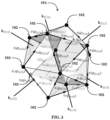
- FIG. 4 depicts a regular icosahedron inscribed in a cube in the manner employed by Longuet-Higgins and Roberts;
- FIG. 5 depicts the proposed nearly-symmetrical nuclear configuration of a boron icosahedron wherein the three-center bonds are described in terms of 24 delocalized tangential atomic orbitals ⁇ i (p ⁇ 111 ⁇ );
- FIG. 6 depicts an energy diagram showing the proposed energy levels of the clustered nuclei of the regular boron icosahedron shown in FIG. 5 ;
- FIG. 7 depicts an energy diagram showing the proposed energy levels of the clustered valence electrons of the regular boron icosahedron shown in FIG. 5 ;
- FIG. 8 is an illustration of a regular boron icosahedron with a symmetrical nuclear configuration shown with four hydrogens bonded by a Debye force;
- FIG. 9 is an illustration of a monocrystalline silicon unit cell
- FIG. 10 is an illustration of a diamond-like picocrystalline unit cell
- FIG. 11 is an energy level diagram depicting the occupied energy levels of the first eight valence electrons obeying Dirac's relativistic wave equation
- FIG. 12 is an energy level diagram depicting the occupied energy levels of the first twelve valence electrons obeying Dirac's relativistic wave equation
- FIG. 13 is an energy level diagram depicting the occupied energy levels of the first twenty-four valence electrons obeying Dirac's relativistic wave equation
- FIG. 14 is an energy level diagram depicting the occupied energy levels of the first thirty-two valence electrons obeying Dirac's relativistic wave equation
- FIG. 15 is an energy level diagram depicting the occupied energy levels of the thirty-six valence electrons obeying Dirac's relativistic wave equation
- FIG. 16 depicts an energy level diagram illustrating a proposed first disentanglement of the
- FIG. 17 depicts an energy level diagram illustrating a proposed second disentanglement of the
- FIGS. 18 A-B depict energy diagrams believed to reflect the occupied energy levels by valence electrons in negatively-ionized and positively-ionized picocrystalline artificial borane atoms B 12 2 ⁇ H 4 and B 12 2+ H 4 101 , due to disproportionation in picocrystalline silaborane p-(B 12 H 4 ) 3 Si;
- FIG. 19 is an illustration of a diamond-like picocrystalline unit cell with the incorporation of natural oxygen atoms
- FIG. 20 depicts an energy level diagram illustrating a proposed disentanglement of the
- FIG. 21 depicts a phonovoltaic cell 400 comprising multiple pairs of contiguous picocrystalline silaborane p-(B 12 H 4 ) 3 Si 5 regions and picocrystalline oxysilaborane p-(B 12 2 ⁇ H 4 ) 2 Si 4 O 2 2+ regions intervened by metallic electrodes;
- FIG. 22 is an another illustration of the Carnot cycle
- FIG. 23 is an illustration of a proposed quantum thermodynamic cycle
- FIGS. 24 A-D depict energy diagrams illustrating the proposed occupied electronic energy levels of the artificial nuclei of the first- and second-nearest neighbor picocrystalline artificial borane atoms 101 of a pair of conjoined picocrystalline silaborane p-(B 12 H 4 ) 3 Si 5 and picocrystalline oxysilaborane p-(B 12 2 ⁇ H 4 ) 2 Si 4 O 2 2+ regions 401 and 402 ;
- FIGS. 25 A-D depict a proposed spontaneous mobile charge diffusion
- FIGS. 26 A-D further depict a proposed mobile charge diffusion
- FIGS. 27 A-D still further depict a proposed mobile charge diffusion
- FIGS. 28 A-D depict a proposed spectral induction of valence electrons from intraicosahedral bonding suborbitals into intraicosahedral antibonding suborbitals in a picocrystalline silaborane p-(B 12 H 4 ) 3 Si 5 region;
- FIGS. 29 A-D depict a proposed self-thermalization of valence electrons in a picocrystalline silaborane p-(B 12 H 4 ) 3 Si 5 region due to the nuclear electric quadrupole moment of the natural boron atoms;
- FIGS. 30 A-D depict a proposed disproportionation in a picocrystalline silaborane p-(B 12 H 4 ) 3 Si 5 region;
- FIG. 31 is an illustration of a proposed quantum thermodynamic cycle
- FIG. 32 is an illustration of the Earth's energy budget
- FIG. 33 is an illustration of the spectral radiance of a blackbody
- FIG. 34 is a micrograph obtain by high-resolution transmission microscopy (HRTEM) of a picocrystalline borane solid deposited on monocrystalline silicon;
- FIG. 35 is an HRTEM fast Fourier transform (FFT) image of the monocrystalline silicon substrate
- FIG. 36 is an FFT image of the picocrystalline borane solid
- FIG. 37 is a graph in terms of interplanar lattice d-spacings of the HRTEM diffraction intensity of the monocrystalline substrate
- FIG. 38 is a graph in terms of interplanar lattice d-spacings of the HRTEM diffraction intensity of the picocrystalline borane solid;
- FIG. 39 is a conventional ⁇ -2 ⁇ x-ray diffraction (XRD) pattern of a self-assembled picocrystalline borane solid
- FIG. 40 is a grazing incidence x-ray diffraction (GIXRD) scan of the same self-assembled picocrystalline borane solid in FIG. 39 ;
- FIG. 41 is a second grazing incidence x-ray diffraction (GIXRD) scan of the same self-assembled picocrystalline borane solid scanned in FIG. 39 ;
- GIXRD grazing incidence x-ray diffraction
- FIG. 42 is an illustration of a silaboride film deposited on a donor-doped region of a monocrystalline substrate
- FIG. 43 is a graph of a GIXRD scan of the picocrystalline silaboride solid of Example 1;
- FIG. 44 is an illustration of an oxysilaborane film deposited over a donor-doped silicon region in accordance with Example 2;
- FIG. 45 is a conventional ⁇ -2 ⁇ x-ray diffraction (XRD) pattern of the thin oxysilaborane solid of Example 2;
- FIG. 46 is a graph of a GIXRD scan of the oxysilaborane solid of Example 2.
- FIG. 47 is an illustration of a silaborane film deposited on an n-type silicon substrate in accordance with Example 3.
- FIG. 48 is an x-ray photoelectron spectroscopy (XPS) depth profile of the silaborane film deposited in Example 3;
- FIG. 49 is an Auger electron spectroscopy (AES) depth profile of the silaborane film deposited in Example 3;
- FIG. 50 is an illustration of a silaborane film deposited on a p-type silicon substrate in accordance with Example 4.
- FIG. 51 is an x-ray photoelectron spectroscopy (XPS) depth profile of the silaborane film deposited in Example 4;
- FIG. 52 is a linear graph of the current-voltage characteristics of the silaborane film deposited in Example 4, as measured by an HP-4145 parameter analyzer with the sweep signals obtained by a mercury probe;
- FIG. 53 is a log-log graph of the current-voltage characteristics of the silaborane film deposited in Example 4, as measured by an HP-4145 parameter analyzer with the sweep signals obtained by a mercury probe;
- FIG. 54 is an illustration of an oxysilaborane film deposited on a p-type silicon substrate in accordance with Example 5;
- FIG. 55 is an x-ray photoelectron spectroscopy (XPS) depth profile of the oxysilaborane film deposited in Example 5;
- FIG. 56 is a linear graph of the current-voltage characteristics of the oxysilaborane film deposited in Example 5, as measured by an HP-4145 parameter analyzer with the sweep signals obtained by a mercury probe;
- FIG. 57 is a log-log graph of the current-voltage characteristics of the oxysilaborane film deposited in Example 5, as measured by an HP-4145 parameter analyzer with the sweep signals obtained by a mercury probe;
- FIG. 58 is an x-ray photoelectron spectroscopy (XPS) depth profile of another embodiment of an oxysilaborane film deposited per Example 6;
- XPS x-ray photoelectron spectroscopy
- FIG. 59 is a linear graph of the current-voltage characteristics of the oxysilaborane film characterized in Example 6, as measured by an HP-4145 parameter analyzer with the sweep signals obtained by a mercury probe;
- FIG. 60 is a log-log graph of the current-voltage characteristics of the oxysilaborane film characterized in Example 6, as measured by an HP-4145 parameter analyzer with the sweep signals obtained by a mercury probe;
- FIG. 61 is an x-ray photoelectron spectroscopy (XPS) depth profile of yet another embodiment of an oxysilaborane film deposited per Example 7;
- XPS x-ray photoelectron spectroscopy
- FIG. 62 is a linear graph of the current-voltage characteristics of the oxysilaborane film characterized in Example 7, as measured by an HP-4145 parameter analyzer with the sweep signals obtained by a mercury probe;
- FIG. 63 is a log-log graph of the current-voltage characteristics of the oxysilaborane film characterized in Example 7, as measured by an HP-4145 parameter analyzer with the sweep signals obtained by a mercury probe;
- FIG. 64 is an x-ray photoelectron spectroscopy (XPS) depth profile of still another embodiment of an oxysilaborane film deposited in Example 8;
- XPS x-ray photoelectron spectroscopy
- FIG. 65 is a linear graph of the current-voltage characteristics of the oxysilaborane film characterized in Example 8, as measured by an HP-4145 parameter analyzer with the sweep signals obtained by a mercury probe;
- FIG. 66 is a log-log graph of the current-voltage characteristics of the oxysilaborane film characterized in Example 8, as measured by an HP-4145 parameter analyzer with the sweep signals obtained by a mercury probe;
- FIG. 67 is an x-ray photoelectron spectroscopy (XPS) depth profile of yet still another embodiment of an oxysilaborane film deposited in Example 9;
- XPS x-ray photoelectron spectroscopy
- FIG. 68 is a linear graph of the current-voltage characteristics of the oxysilaborane film characterized in Example 9, as measured by an HP-4145 parameter analyzer with the sweep signals obtained by a mercury probe;
- FIG. 69 is a log-log graph of the current-voltage characteristics of the oxysilaborane film characterized in Example 9, as measured by an HP-4145 parameter analyzer with the sweep signals obtained by a mercury probe;
- FIG. 70 is an illustration of a p-isotype electrochemical rectifier comprising oxysilaborane film produced in accordance with Example 10;
- FIG. 71 is a linear graph of the current-voltage characteristics of the p-isotype electrochemical rectifier in Example 10, as measured by an HP-4145 parameter analyzer with the sweep signals obtained by microprobes;
- FIG. 72 is a linear graph of a different current-voltage range of the p-isotype electrochemical rectifier in Example 10, as measured by an HP-4145 parameter analyzer with the sweep signals obtained by microprobes;
- FIG. 73 is a log-log graph of forward-bias current-voltage characteristics of the p-isotype electrochemical rectifier in Example 10, as measured by an HP-4145 parameter analyzer with the sweep signals obtained by microprobes;
- FIG. 74 is a log-log graph of reverse-bias current-voltage characteristics of the p-isotype electrochemical rectifier in Example 10, as measured by an HP-4145 parameter analyzer with the sweep signals obtained by microprobes;
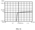
- FIG. 75 is a linear graph of the current-voltage characteristics of the p-isotype electrochemical rectifier in Example 11, as measured by an HP-4145 parameter analyzer with the sweep signals obtained by microprobes;
- FIG. 76 is a linear graph of a different current-voltage range of the p-isotype electrochemical rectifier in Example 11, as measured by an HP-4145 parameter analyzer with the sweep signals obtained by microprobes;
- FIG. 77 is a log-log graph of forward-bias current-voltage characteristics of the p-isotype electrochemical rectifier in Example 11, as measured by an HP-4145 parameter analyzer with the sweep signals obtained by microprobes;
- FIG. 78 is a log-log graph of reverse-bias current-voltage characteristics of the p-isotype electrochemical rectifier in Example 11, as measured by an HP-4145 parameter analyzer with the sweep signals obtained by microprobes;
- FIG. 79 is a linear graph of a first current-voltage range of the p-isotype electrochemical rectifier in Example 12, as measured by an HP-4145 parameter analyzer with the sweep signals obtained by means of microprobes;
- FIG. 80 is a linear graph of a second current-voltage range of the p-isotype electrochemical rectifier in Example 12, as measured by an HP-4145 parameter analyzer with the sweep signals obtained by means of microprobes;
- FIG. 81 is a linear graph of a third current-voltage range of the p-isotype electrochemical rectifier in Example 12, as measured by an HP-4145 parameter analyzer with the sweep signals obtained by means of microprobes;
- FIG. 82 is a log-log graph of forward-bias current-voltage characteristics of the p-isotype electrochemical rectifier in Example 12, as measured by an HP-4145 parameter analyzer with the sweep signals obtained by microprobes;
- FIG. 83 is a log-log graph of reverse-bias current-voltage characteristics of the p-isotype electrochemical rectifier in Example 12, as measured by an HP-4145 parameter analyzer with the sweep signals obtained by microprobes;
- FIG. 84 is an illustration of an electrochemical device comprising a silaborane film produced in accordance with Example 13;
- FIG. 85 is a linear graph of the current-voltage characteristics of the electrochemical device in Example 13, as measured by an HP-4145 parameter analyzer with the sweep signals obtained by microprobes;
- FIG. 86 is a linear graph of a second current-voltage characteristics of the electrochemical device in Example 13, as measured by an HP-4145 parameter analyzer with the sweep signals obtained by microprobes;
- FIG. 87 is a log-log graph of forward-bias current-voltage characteristics of the electrochemical device in Example 13, as measured by an HP-4145 parameter analyzer with the sweep signals obtained by microprobes;
- FIG. 88 is a log-log graph of reverse-bias current-voltage characteristics of the electrochemical device in Example 13, as measured by an HP-4145 parameter analyzer with the sweep signals obtained by microprobes;
- FIG. 89 is an illustration of an oxysilaborane film deposited on a p-type silicon substrate in accordance with Example 14;
- FIG. 90 is an x-ray photoelectron spectroscopy (XPS) depth profile of the oxysilaborane film deposited in Example 14;
- FIG. 91 is an illustration of the thermal processing budget of the oxysilaborane film deposited in Example 14;
- FIG. 92 is a geometric representation of an energy equilibration proposed by Josiah Willard Gibbs;
- FIG. 93 is a geometric representation of an entropy equilibration proposed by Josiah Willard Gibbs;
- FIGS. 94 A-B is an illustration comparing a phonovoltaic cell and a photovoltaic cell in the dark;
- FIGS. 95 A-B is an illustration comparing a phonovoltaic cell and a photovoltaic cell in which mobile electron-hole pairs are radiatively induced;
- FIGS. 96 A-B is an illustration comparing a phonovoltaic cell and a photovoltaic cell in which induced mobile electron-hole pairs are separated;
- FIGS. 97 A-B is an illustration comparing a phonovoltaic cell and a photovoltaic cell in which an electrical load is impressed;
- FIG. 98 is projected manufacturing cost analysis of a phonovoltaic cell
- FIGS. 99 A-C is an illustration comparing a phonovoltaic cell, a photovoltaic cell, and a thermionic converter
- FIG. 100 is an illustration of a device comprising an oxysilaborane film and gold produced in accordance with Example 15;
- FIG. 101 is an x-ray photoelectron spectroscopy (XPS) depth profile of the oxysilaborane film deposited in Example 15;
- XPS x-ray photoelectron spectroscopy
- FIG. 102 is secondary ion mass spectroscopy (SIMS) performed to measure a trace impurity concentration of gold in the oxysilaborane film in Example 15;
- SIMS secondary ion mass spectroscopy
- FIG. 103 depicts metal electrodes 536 and 537 evaporated over the gold film containing device of Example 15;
- FIG. 104 is a linear graph of the current-voltage characteristics of the oxysilaborane film in Example 15;
- a regular icosahedron is inscribed in a cube in FIG. 4 such that the coordinates of the icosahedral vertices are described, subject to Eq. (21), in terms of the following position coordinates: ( ⁇ , ⁇ 1,0), (0, ⁇ , ⁇ 1), and ( ⁇ 1, 0, ⁇ ).
- any orientation along, or parallel to, any cubic edge is generally represented by 100 .
- Any particular 100 orientation e.g. the [010] orientation along the positive y-axis, will be specifically denoted.
- a cubic face, or a plane parallel to a cubic face is generally represented by ⁇ 100 ⁇ .
- a particular ⁇ 100 ⁇ plane, e.g. the xz-plane normal to the [010] direction, is represented by (010).
- a particular 100 orientation, e.g. the [010] orientation is always normal to the corresponding ⁇ 100 ⁇ plane, viz. the (010) plane in this case.
- any orientation along, or parallel to, a cubic body diagonal is represented by 111 .
- icosahedral faces There are two classes of icosahedral faces: 8 icosahedral faces are constituted by ⁇ 111 ⁇ planes normal to a 111 cubic body diagonal and 12 icosahedral faces are constituted by ⁇ ⁇ 1 0 ⁇ planes intersecting in pairs along a 100 orientation. Three-center bonds exist along edges of the ⁇ 111 ⁇ planes.
- a molecular orbital analysis which describes the three-center boron bonds by a generalization of the methodology of Longuet-Higgins and Roberts performed in [0020]-[0063] of U.S. Provisional Application No. 62/591,848, is incorporated herein by reference.
- That generalized molecular orbital analysis describes a regular boron icosahedron 104 comprising 12 boron nuclei 102 , with a nearly-symmetrical nuclear configuration, that is constituted by 24 delocalized atomic orbitals ⁇ i (p ⁇ 111 ⁇ ) in a nearly-spherical spheroid wherein displacement is ideally limited to the 8 wave vectors.
- the boron icosahedron 104 in FIG. 5 is referred to herein as an artificial nucleus 104 .
- short-range periodic translational order is defined as a regular repetition of atomic positions over a space substantially confined to only first- and second-nearest neighbor atoms.
- the artificial nucleus 104 represented in FIG. 5 exhibits a short-range periodic translational order in which the 12 boron nuclei 102 ideally remain stationary at the 12 icosahedral vertices, such that all icosahedral displacement is ideally limited to only periodic vibrations along the 8 wave vectors.
- the artificial nucleus 104 in FIG. 5 constitutes a quantum Floquet-many-body subsystem that behaves similar to the nucleus of a natural carbon atom.
- a quantum Floquet-many-body system is a time-dependent many-body system that is periodic over time by virtue of its own dynamics. In order to understand preferred embodiments of this invention, it is purposeful to establish the quantum entanglement of the atomic orbitals ⁇ i (p ⁇ 111 ⁇ ) forming the quantum Floquet-many-body subsystem of the artificial nucleus 104 .
- the analysis of the artificial nucleus 104 in FIG. 5 was performed in terms of the group analysis of a regular icosahedron.
- the icosahedral symmetry group I h is unique amongst all the other symmetry groups in that it possesses the largest number of symmetry operations ( 120 ) of any symmetry group in Nature.
- the largest number of symmetry operations allowed in any crystallographic point group is 48, such that the icosahedral symmetry group I h is not a crystallographic point group that can support spatial crystals which exhibit a long-range periodic translational order.
- the inability of the icosahedral symmetry group I h to support a long-range periodic translational order allows it to, more generally, support an intrinsic spontaneous time-translational symmetry breaking to be described.
- FIG. 5 The believed energy levels of the 12 boron nuclei 102 forming the artificial nucleus 104 are shown in FIG. 6 .
- the energy levels of the 36 valence electrons of the artificial nucleus 104 are shown in FIG. 7 .
- the nuclear energy levels in FIG. 6 and the electronic energy levels in FIG. 7 satisfy the energy eigenvalues of Dirac's relativistic wave equation. It is believed that the artificial nucleus 104 shown in FIG. 5 constitutes a quantum Floquet-many-body system analogous to that of the natural nucleus of carbon 6 12 C.
- the artificial nucleus 104 in FIG. 5 constitutes a manifestation of the quantum Floquet-many-body fermion system with the highest possible degree of symmetry in Nature.
- a fermion is a subatomic particle, subject to the Pauli exclusion principle, which is characterized by Fermi-Dirac statistics, as well as, any composite particle comprised of an odd number of said subatomic particles.
- a quantum Floquet-many-body system comprising fermions at the vertices of a regular icosahedron will be hereinafter referred to as an icosahedral Floquet-many-fermion system.
- the 12 boron nuclei 102 of the artificial nucleus 104 are initially assumed to be boron 5 10 B nuclei comprising an odd number of both protons and neutrons.
- An incorporation of the other natural boron isotope 5 11 B will be later considered hereinbelow.
- the icosahedral Floquet-many-fermion system of the particular artificial nucleus 104 in FIG. 5 possesses the highest degree of degree of symmetry in Nature relative to the icosahedral vertices at which the 12 boron nuclei 102 reside. This symmetry is exhibited by the 12 nucleons of carbon 6 12 C.
- point displacement There exist only two types of point displacement, viz. translation along a rectilinear axis and rotation about a rectilinear axis. Translation and rotation exhibit contrary displacements of points, such as the twelve icosahedral vertices of an icosahedral Floquet-many-fermion system.
- the great circles associated with the quadrupole spherical harmonics contain the wave vectors of the artificial nucleus 104 in FIG. 5 . This is consistent with the displacement of an icosahedral Floquet-many-fermion system in Eqs. (22a-d).
- the symmetry analysis of the artificial nucleus 104 in FIG. 5 is of a general nature, without any commitment as to the physical size of the icosahedral Floquet-many-fermion system.
- the distance between opposite icosahedral faces of the artificial nucleus 104 is ideally 269 pm, such that it is specifically referred to as an icosahedral Floquet-many-fermion picocrystal.
- the distance between the opposite icosahedral faces of the natural nucleus of carbon 6 12 C can be measured in terms of femtometers, such that the natural nucleus of carbon 6 12 C constitutes an icosahedral Floquet-many-fermion femtocrystal. It is believed that the artificial nucleus 104 exhibits the same symmetry as the natural nucleus of carbon 6 12 C.
- Jahn-Teller effect results in a symmetry-breaking that lifts electronic orbital degeneracies by normal displacements of the 12 boron nuclei 102 , known as Jahn-Teller-active modes, that distort polyatomic ions and molecules in the absence of spin-orbit coupling.
- Preferred embodiments of the invention constitute novel and useful embodiments of a quantum thermodynamics capable of supporting a quantum thermodynamic cycle that self-thermalizes, so as to eliminate the dependence of a heat engine on fuels.
- the novel and useful embodiments of this invention cannot be described by means of classical thermodynamics due to the role of quantum entanglement.
- Einstein formed this conclusion by a consideration of the relativistic translational Doppler shift of a radiative body. In extending his special theory of relativity to include rotation in his general theory of relativity, Einstein was unable to derive a relativistic rotational Doppler shift.
- a rotating fermion since a rotating fermion necessarily emits radiation, then a rotating fermion can only stabilize as a member of a quantum many-body system in which pairs of complementary rotational Doppler shifts stabilize said quantum many-body system.
- the icosahedral Floquet-many-fermion picocrystal of the artificial nucleus 104 constitutes a stabilized quantum many-body system of fermions that can be described by Dirac's relativistic wave equation. Dirac's energy eigenvalues for a Dirac many-body system of fermions obtained within [0086]-[0167] of U.S. Provisional Application No. 62/591,848 are incorporated herein by reference.
- Fusion is generally taken herein to be any process in which fermions are bonded together by the transformation of a quantity of matter in into energy.
- a Dirac quasiparticle is a quantum Floquet-many-fermion system due to a dynamic interaction between fermions that entangles the individual energy levels.
- mc 2 - E + a 2 ⁇ mc 2 2 ⁇ n 2 + a 4 ⁇ mc 2 2 ⁇ ⁇ ⁇ n 3 > 0 E > 0 ( 25 ⁇ a )
- mc 2 - E - a 2 ⁇ mc 2 2 ⁇ n 2 - a 4 ⁇ mc 2 2 ⁇ ⁇ ⁇ n 3 ⁇ 0 E ⁇ 0 ( 25 ⁇ b )
- the first term on the right side of Eq. (25a) comprises energy eigenvalues obeying Schrödinger's wave equation.
- the successive higher-order shells thus comprise lower bound-energy eigenstates.
- the orbital angular momentum remains degenerate in the bound-energy eigenstates obeying Schrödinger's equation. This degeneracy is lifted by Dirac's equation.
- the second bound-energy term on the right side of Eq. (25a) is due to the fine structure of a spinning fermion.
- the salient properties of a fermion fine structure are cogently described in order to better understand real-world devices comprising preferred embodiments of this invention.
- quantum chemistry involves a finite variation in the quantity of matter of the chemical reactants and products due to fusion.
- the role of quantum chemistry in this invention will be further discussed below.
- the concept of apeiron was initially conceived by Anaximander of Miletus circa 585 BC.
- the ability to exploit electric charge e in a quantum thermodynamic cycle, capable of replacing a Carnot cycle, can only be achieved when electric charge e is provided a mechanical basis.
- the mechanical basis of electric charge e is fundamentally derived in [0794]-[0846] of U.S. Provisional Application No. 62/591,848 and incorporated herein by reference.
- Wien's spectral displacement law supports the following spectral displacement (i.e., a shift in frequency) at the constant irradiance
- Spectral displacement is capable of quantum mechanically supporting a heat engine.
- ⁇ dot over (s) ⁇ is the phase velocity of electromagnetic radiation.
- ⁇ dot over (s) ⁇ >0 work is done upon electromagnetic radiation in order to cause it to undergo a spectral displacement from some lower frequency interval (v,v+dv) into a higher frequency interval (v′,v′+dv′).
- v,v+dv some lower frequency interval
- v′,v′+dv′ a higher frequency interval
- Kirchhoff's universal function K(v,T) at the infrared spectral extreme hv ⁇ kT is dominated by the continuous thermal resonator energy kT while, very differently, Kirchhoff's universal function K(v,T) near the ultraviolet spectral extreme hv>>kT is dominated by the discrete vibrational energy hv n k .
- K ⁇ ( v , T ) 2 ⁇ v 2 c 2 ⁇ kT ⁇ ⁇ hv ⁇ ⁇ ⁇ kT ( 36 ⁇ a )
- K ⁇ ( v n ⁇ , T ) 2 ⁇ [ v n ⁇ c ] 2 ⁇ h ⁇ v n ⁇ ⁇ exp ⁇ [ - h ⁇ v n ⁇ kT ] ⁇ ⁇ hv n ⁇ ⁇ >> kT ( 36 ⁇ b )
- Einstein's molar heat capacity in Eq. (20) can be simplified as follows for a low-frequency Planckian resonator frequency, such that hv ⁇ kT.
- a picocrystalline artificial borane atom 101 constitutes: (1) an artificial nucleus 104 formed by a boron icosahedron comprising 12 natural boron nuclei 102 with a nearly-symmetrical nuclear configuration and (2) 4 artificial valence electrons constituted by 4 natural hydrogen atoms with the hydrogen nuclei 103 bonded to a boron icosahedron such that the 4 hydrogen valence electrons are aligned along a wave vector.
- the picocrystalline artificial borane atom 101 comprises a boron icosahedron with 36 boron valence electrons occupying intraicosahedral molecular orbitals, such that intericosahedral chemical bonds are by the hydrogen valence electrons.
- An electric quadrupole moment along the vectors causes an electric dipole moment in hydrogen atoms, such that the hydrogen nuclei 103 bond by a Debye force to the artificial nucleus 104 .
- a chemical bonding of the picocrystalline artificial borane atoms 101 is explained by a self-selective atomic replacement in the monocrystalline silicon unit cell 200 in FIG. 9 , which is comprised of 8 silicon vertex atoms 201 , 6 silicon face-center atoms 202 , as well as, 4 silicon basis atoms 203 .
- the 4 basis atoms 203 reside along a 111 cubic body diagonal in a tetrahedral arrangement.
- the monocrystalline silicon unit cell 200 is periodically translated over space so as to form a monocrystalline silicon lattice wherein the silicon vertex atoms 201 and the silicon face-center atoms 202 are covalently bonded to, and only to, the four silicon basis atoms 203 along a 111 crystal orientation.
- the resultant monocrystalline silicon lattice has a long-range periodic translational order in terms of cubic unit cells of ⁇ 0.5431 nm along each edge, without any 100 chemical bonds.
- a diamond-like picocrystalline silaborane unit cell 300 is constructed by replacing each silicon vertex atom 201 within the monocrystalline silicon unit cell 200 with a borane molecule 101 , as shown in FIG. 10 .
- the 8 borane molecules 101 at the vertices of the silaborane unit cell 300 in FIG. 10 are shared amongst 8 picocrystalline silaborane unit cells 300 in an extended solid lattice (not shown).
- the periodic translation of the picocrystalline silaborane unit cell 300 over space would, thereby, result in a picocrystalline silaborane (B 12 H 4 )Si 7 solid lattice that effectively acts as a self-assembled diamond-like picocrystalline lattice structurally similar to monocrystalline silicon.
- Picocrystalline artificial borane atoms 101 in FIG. 8 with a nearly-symmetrical nuclear configuration, replace the 8 silicon vertex atoms 201 in FIG. 10 in the picocrystalline silaborane (B 12 H 4 )Si 7 lattice.
- the picocrystalline oxysilaboranes of this invention constitute nearly transparent solids that are believed to be formed by a continuous random network of polyatomic unit cells obeying a modification of rules developed by Zachariasen in a paper “The Atomic Arrangement in Glass,” Journal of the American Chemical Society , Vol. 54, 1932, pp. 3841-3851. All references hereinafter to Zachariasen are understood as referring to this paper. Zachariasen focused on oxide glasses and, more particularly, on amorphous SiO 2 and amorphous B 2 O 3 . Zachariasen proved that amorphous SiO 2 is constituted by a continuous random network of SiO 4 tetrahedra. Similarly, the picocrystalline oxysilaboranes are believed to be constituted by the continuous random network of polyhedra with a nearly-symmetrical boron icosahedron at each of the eight polyhedra corners.
- picocrystalline oxysilaboranes constitute solids formed by the continuous random network of borane hexahedra which, by definition, are constituted by hexahedra with picocrystalline artificial borane atoms 101 at the hexahedral corners.
- the monocrystalline silicon unit cell 200 portrayed in FIG. 9 is a regular hexahedron (cube)
- the diamond-like picocrystalline silaborane unit cell 300 in FIG. 10 while portrayed for description purposes as a cube, is in actuality an irregular hexahedron.
- Zachariasen represented the atomic arrangement of an oxide glass by the continuous random network of polymorphic oxygen tetrahedra or triangles
- the atomic arrangement in a borane solid is described by a random network of irregular hexahedra.
- the eight corners of the borane hexahedron 300 in FIG. 10 are comprised of picocrystalline artificial borane atoms 101 .
- Each corner picocrystalline artificial borane atom 101 is, ideally, bonded to four tetravalent natural atoms 303 which are surrounded by eight corner picocrystalline artificial borane atoms 101 .
- the preferred tetravalent natural atoms 303 are natural silicon atoms.
- Each of the tetravalent natural atoms 303 bonds to one or more face-center atom 302 in the borane hexahedron 300 shown in FIG. 10 .
- Each face-center atom 302 can be any of, but not limited to: a tetravalent natural atom such as silicon; a hexavalent natural atom such as oxygen; or, possibly, a tetravalent picocrystalline artificial borane atom 101 .
- a tetravalent natural atom such as silicon
- a hexavalent natural atom such as oxygen
- a tetravalent picocrystalline artificial borane atom 101 a tetravalent natural atom such as silicon
- a hexavalent natural atom such as oxygen
- picocrystalline artificial borane atom 101 a tetravalent picocrystalline artificial borane atom 101 .
- each corner picocrystalline artificial borane atom 101 covalently bonds to four tetravalent natural atoms 303 along a 111 crystalline orientation. It is noteworthy to recognize that the tetravalent natural atoms 303 are in the positions of the silicon basis atoms 203 (as shown in FIG. 9 in the unit cell of monocrystalline silicon) that undergo a spatial displacement to preserve the unit cell dimension.
- each irregular borane hexahedron 300 forming a solid lattice is ideally constituted by 8 corner picocrystalline artificial borane atoms 101 , 6 face-center picocrystalline artificial borane atoms 101 , and 4 natural silicon atoms 303 .
- picocrystalline silaborane (B 12 H 4 ) 4 Si 4 forms a picocrystalline polymorph, similar to monocrystalline silicon, comprised of tetravalent natural silicon atoms 303 and tetravalent picocrystalline artificial borane atoms 101 . It is by means of this type of structure that spin-orbit coupling becomes physically important.
- Preferred embodiments of this invention involve a type of order not known in the prior art.
- Long-range periodic translational order is defined herein as the regular repetition of a certain invariant arrangement of atoms, known as a unit cell, through space so as to thereby form a translationally-invariant tiling in a regular array of natural atoms well beyond first- and second-nearest neighbor natural atoms.
- Monocrystalline and polycrystalline materials exhibit a long-range periodic translational order throughout space. The periodic repetition of atomic positions is preserved throughout the entire space of a monocrystalline material. In a polycrystalline material, the periodic repetition of atomic positions is maintained over the limited finite space in grains, which can be themselves arbitrarily oriented over space.
- a nanocrystalline material is any polycrystalline material in which the grain sizes range between 300 pm and 300 nm.
- Short-range periodic translational order is defined hereinafter as the repetition of natural atomic positions over a space substantially confined to only the first- and second-nearest neighbor natural atoms.
- the radii of isolated neutral atoms range between 30 and 300 pm.
- any picocrystalline material is a material exhibiting a short-range periodic translational order confined to repeating atomic positions in finite groups of first- and second-nearest neighbor natural atoms.
- An amorphous material as used hereinafter, is a material void of regularly repeating arrangements of atoms, so as to thus be incapable of supporting a constructive interference of x-rays.
- Short-range periodic translational order is dominant in picocrystalline silaborane (B 12 H 4 ) 4 Si 4 .
- a “picocrystalline artificial atom” is a cluster, of a size less than 300 pm, of natural atoms that are mutually bonded together so as to support a short-range periodic translational order and an internal discrete quantization of energy levels.
- special types of picocrystalline artificial atoms can be bonded to other natural atoms in order to form an extended lattice of natural atoms and picocrystalline artificial atoms.
- a natural atom is any isotope of a stable chemical element contained in the periodic chart.
- a special type of picocrystalline artificial atom comprises a boron icosahedron with a nearly-symmetrical nuclear configuration.
- Preferred embodiments of this invention remedy scaling limitations of monolithic integrated circuits by a material amalgamation of monocrystalline silicon and graphene that supports a displacement of electrical action over space.
- picocrystalline artificial borane atoms 101 replace the silicon vertex atoms 201 in FIG. 10 .
- picocrystalline silaborane (B 12 H 4 ) 4 Si 4 the six face-center atoms 302 are (although not shown in FIG. 10 ) picocrystalline artificial borane atoms 101 .
- picocrystalline silaborane (B 12 H 4 ) 4 Si 4 does not possess any long-range periodic translational order in the manner of monocrystalline silicon.
- picocrystalline silaborane (B 12 H 4 ) 4 Si 4 cannot physically support extended conduction and valence energy bands over space.
- the existence of van der Waals forces (and more particularly, Debye forces) between picocrystalline artificial borane atoms 101 further eliminates extended conduction and valence energy bands over space in picocrystalline silaborane (B 12 H 4 ) 4 Si 4 .
- the icosahedral symmetry of the picocrystalline artificial borane atoms 101 gives rise to a highly novel type of displacement of electrical action which is not known in the prior art.
- the profound novelty and utility of preferred embodiments of this invention consider the low-frequency extremes of Eqs. (36a-b).
- K ⁇ ( v , T ) 2 ⁇ v 2 c 2 ⁇ kT ⁇ ⁇ hv ⁇ ⁇ ⁇ kT ( 41 ⁇ a )
- K ⁇ ( v n ⁇ , T ) 2 ⁇ [ v n ⁇ c ] 2 ⁇ h ⁇ v n ⁇ ⁇ ⁇ hv n ⁇ ⁇ ⁇ ⁇ kT ( 41 ⁇ b )
- the quantum temperature ⁇ T 0.77° K of the artificial nucleus 104 is well below the absolute temperature 2.72° K associated with the cosmic microwave background radiation.
- the quantum temperature ⁇ T of the continuous thermal resonator is much greater than the ambient temperature T. Since the artificial nuclei 104 forming picocrystalline silaborane (B 12 H 4 ) 4 Si 4 constitute open icosahedral Floquet-many-fermion picocrystals, then the quantum temperature ⁇ T of any artificial nucleus 104 is clamped at the ambient temperature T.
- FIG. 11 four electrons initially occupy the +2p 3/2 4 antibonding suborbital and four electrons initially occupy the ⁇ 2p 3/2 4 bonding suborbital of a Dirac quasiparticle.
- Two consequences of FIG. 11 distinguish Dirac quasiparticles from fermions obeying Schrödinger's nonrelativistic wave equation.
- spectral induction is not known in the prior art, it is used in the successful operation of preferred embodiments of the present invention.
- the bound-energy eigenstates of a Dirac quasiparticle are involved in the chemical fusion of boron icosahedra comprising preferred embodiments of this invention.
- Spin-orbit coupling separates whole-integer-quantized orbitals into doublets of positive-energy half-integer-quantized suborbitals (n>0) per FIG. 11 .
- spin-orbit coupling separates whole-integer-quantized orbitals into pairs of negative-energy half-integer-quantized suborbitals (n ⁇ 0) in FIG. 11 .
- the half-integer-quantized suborbitals in FIG. 11 obey the energy eigenvalues of a Dirac quasiparticle in Eqs. (23a-b).
- the quantum entanglement of the half-integer-quantized suborbitals of a Dirac quasiparticle results in the highest-energy level in each shell possessing the highest bound energy in said shell. This seemingly strange phenomenon (which is further discussed hereinbelow) will be described in terms of relative changes in the Gibbs free energy.
- ⁇ 2sp 1/2 0 eigenstates, in FIG. 11 is due to the fact that the Gibbs free energy of the
- a principal attribute of the artificial nucleus 104 comprising the picocrystalline oxysilaboranes of this invention is the existence of excited eigenstates of a lower Gibbs free energy than that of the ground eigenstate in each shell.
- the stable unfilled shell condition in FIG. 11 is due to a spontaneous excitation of valence electrons into the higher-angular-momentum suborbital of a doublet generated by spin-orbit coupling.
- This spontaneous excitation of electrons is due to a decrease in Gibbs free energy in the higher-angular-momentum eigenstates
- the n ⁇ 2 shells are completely closed if valence electrons fill the
- +3s 1/2 eigenstate is positive, such that electrons are elevated by spin-orbit coupling.
- ⁇ 3s 1/2 eigenstate is positive-definite, such that valence electrons are lowered by spin-orbit coupling.
- +3d 5/2 )>0 in Eq. (45a) causes electrons to occupy the
- a Dirac quasiparticle physically constituted by a boron icosahedron, with a nearly-symmetrical nuclear configuration is a quantum many-body system that is ideally closed to its surroundings due to entangled intraicosahedral antibonding and bonding orbitals occupied by valence electrons in the manner shown in FIG. 15 .
- a boron icosahedron, with a nearly-symmetrical nuclear configuration can be transformed into a semi-open quantum many-body system able to interact with its surroundings due to the boron nuclei.
- An oblate spheroidal nucleus exhibits a negative electric quadrupole moment and, conversely, a prolate spheroidal nucleus exhibits a positive electric quadrupole moment.
- boron 5 10 B constitutes the stable nuclide exhibiting the largest nuclear electric quadrupole moment per nucleon, due to a deformed nucleus.
- Boron 5 10 B has a nuclear angular momentum 3 ⁇ and a large positive nuclear electric quadrupole moment of +0.085 ⁇ 10 ⁇ 28 e-m 2 whereas boron 5 11 B has a nuclear angular momentum 3/2 ⁇ and, also, a nuclear electric quadrupole moment of +0.041 ⁇ 10 ⁇ 28 e-m 2 .
- the energy associated with the nuclear electric quadrupole moment of the boron nuclei is expressed as follows with the aid of Gauss' law.
- This energy is associated with the disentanglement of the
- the concentration of picocrystalline artificial borane atoms 101 in picocrystalline silaborane (B 12 H 4 ) 4 Si 4 is ⁇ 10 22 cm ⁇ 3
- a self-thermalization of picocrystalline artificial borane atoms 101 causes picocrystalline silaborane (B 12 H 4 ) 4 Si 4 to essentially behave as a p-type semiconductor. This is due to the fact that the local disentanglement of the
- picocrystalline silaborane (B 12 H 4 ) 4 Si 4 undergoes a disproportionation that causes an ionization of the partially-disentangled picocrystalline artificial borane atoms 101 into pairs of dianions and dications.
- p-type picocrystalline silaborane is better chemically represented as p-(B 12 H 4 ) 3 Si 5 .
- ⁇ 2 is the square of the fine structure constant—which provides an approximate magnitude of a trace disproportionation of dianion-dication pairs in p-type picocrystalline silaborane p-(B 12 H 4 ) 3 Si 5 .
- p-type picocrystalline silaborane p-(B 12 H 4 ) 3 Si 5 is a semi-open mixed quantum many-body system comprising ⁇ 10 18 cm ⁇ 3 ionized picocrystalline artificial borane atoms 101 B 12 2 ⁇ H 4 and B 12 2+ H 4 distributed amongst ⁇ 10 22 cm ⁇ 3 picocrystalline artificial borane atoms 101 B 12 H 4 which host the p-type picocrystalline silaborane p-(B 12 H 4 ) 3 Si 5 solid.
- An ionization of the artificial nuclei 104 of stationary picocrystalline artificial borane atoms 101 provides for a charge displacement by means of free charge trapped in various artificial nuclei 104 .
- Disproportionation gives rise to a trace concentration of oppositely-ionized pairs of picocrystalline artificial borane atoms 101 B 12 2 ⁇ H 4 and B 12 2+ H 4 .
- the total concentration of neutral picocrystalline artificial borane atoms 101 B 12 H 4 is ⁇ 10 22 cm ⁇ 3 while a much smaller trace concentration of the ionized picocrystalline artificial borane atoms 101 B 12 2 ⁇ H 4 and B 12 2+ H 4 is ⁇ 10 18 cm ⁇ 3 . It is to be understood that an ionization of two neutral picocrystalline artificial borane atoms 101 B 12 H 4 is by virtue of the ionization of the associated artificial nuclei 104 B 12 2 ⁇ and B 12 2+ .
- Electric charge can become self-trapped within an induced potential well, so as to be displaced through space with the self-trapped potential well as a quasiparticle.
- This type of quasiparticle is referred to as a polaron.
- the pair of trapped charges in a bipolaron can generally be either a pair of electrons or a pair of holes.
- Boron-rich solids are particularly well suited for bipolaron formation due to the strong tendency of boron icosahedra to ionize, B 12 ⁇ B 12 2 ⁇ , in order to attain an electronic stability by filling unoccupied intraicosahedral bonding orbitals.
- Mobile charge displacement is sufficiently different in the picocrystalline oxysilaboranes that it is better described in terms of a special type of bipolaron.
- the contributions to the Seebeck coefficient by a carrier-induced softening of the lattice vibrations and by the hopping of singlet softening bipolaronic hole-pairs are largely insensitive to a compositional variation. There exists a variation in the Seebeck coefficient over a compositional range of boron carbide B 12+x C 3 ⁇ x due, in part, to disproportionation.
- Disproportionation in boron carbide is extremely different from that in picocrystalline silaborane p-(B 12 H 4 ) 3 Si 5 due to the Jahn-Teller distortion of the boron icosahedra in boron carbide.
- the electronic orbital degeneracies are lifted in picocrystalline silaborane p-(B 12 H 4 ) 3 Si 5 by spin-orbit coupling, so as to maintain a symmetrical nuclear configuration that escapes Jahn-Teller distortion. In their paper, Jahn and Teller ignored spin effects.
- the three-center chemical bonds supporting boron icosahedra with a symmetrical nuclear configuration, in FIG. 5 result in vibrations along the wave vectors normal to the three-center bonds, per Eqs. (22a-d), due to intertwined rotational and vibrational degrees of freedom.
- Disproportionation is an irreversible non-cyclic process in which the entropy of mixing is maximized per the second law of thermodynamics.
- the fraction of ionized borane molecules that are ionized into borane dications is designated by c.
- Picocrystalline silaborane p-(B 12 H 4 ) 3 Si 5 is thereby said to possess a large quantum electronegativity.
- Picocrystalline oxysilaborane p-(B 12 2 ⁇ H 4 ) 2 Si 4 O 2 2+ conversely possesses a low quantum electronegativity due to totally disentangled intraicosahedral negative-energy bonding eigenstates.
- the phonovoltaic cell 400 is, generally, constituted by any number of such pairs of conjoined regions 401 and 402 intervened by metallic electrodes 403 .
- Any two conjoined picocrystalline silaborane p-(B 12 H 4 ) 3 Si 5 and oxysilaborane p-(B 12 2 ⁇ H 4 ) 2 Si 4 O 2 2+ regions constitute, respectively, the anode region 401 and the cathode region 402 of a p-isotype rectifier 404 .
- a phonovoltaic cell 400 is comprised of a number of p-isotype rectifiers 404 intervened by metal electrodes 403 , with aluminum being the preferred metal.
- the picocrystalline oxysilaborane p-(B 12 2 ⁇ H 4 ) 2 Si 4 O 2 2+ region 402 is substantially void of mobile holes
- the conjoined picocrystalline silaborane p-(B 12 H 4 ) 3 Si 5 anode region 401 at room temperature contains mobile holes at the trace concentration of ⁇ 10 18 cm ⁇ 3 .
- picocrystalline silaborane p-(B 12 H 4 ) 3 Si 5 exhibits an infinite Seebeck coefficient of mixing due to the absence of bipolaronic hole-pairs under ideal conditions.
- the occupied energy levels of the boron icosahedra that comprise picocrystalline silaborane p-(B 12 H 4 ) 3 Si 5 are, ideally, represented in FIGS. 18 A-B .
- the occupied energy levels of the boron icosahedra that comprise picocrystalline oxysilaborane p-(B 12 2 ⁇ H 4 ) 2 Si 4 O 2 2+ are, ideally, further represented within FIG. 20 .
- the conjoined regions 401 and 402 in the phonovoltaic cell 400 support the diffusion of bipolaronic hole-pairs from each picocrystalline silaborane p-(B 12 H 4 ) 3 Si 5 region 401 into the conjoined picocrystalline oxysilaborane p-(B 12 2 ⁇ H 4 ) 2 Si 4 O 2 2+ region 402 .
- Bipolaronic hole-pairs diffuse on their own accord from the
- a mixing of mobile holes between the anode and cathode regions 401 and 402 of each p-isotype rectifier 404 is due to conjoined regions of different compositions.
- the mixing of the mobile holes between the anode region 401 and the cathode region 402 is an irreversible process that proceeds on its own accord until the entropy of mixing S mix is maximized.
- This process can be continuously sustained in the phonovoltaic cell 400 shown in FIG. 21 if, and only if, electric charge delivered to an electrical load is fully replenished by the self-thermalization and disproportionation of mobile electron-hole pairs in the picocrystalline silaborane p-(B 12 H 4 ) 3 Si 5 anode region 401 of each p-isotype rectifier 404 .
- This can be better explained in terms of a quantum thermodynamic cycle that generalizes a Carnot cycle.
- the power stroke of the Carnot cycle within FIG. 22 is the adiabatic expansion A ⁇ B of the ideal gas working substance under spontaneous cooling.
- the ideal gas working substance is spontaneously cooled from the elevated temperature T 0 +dT until it is clamped at the lower ambient temperature T 0 .
- Thermomechanical work is performed by the working substance during adiabatic expansion A ⁇ B.
- the power stroke of the quantum thermodynamic cycle in FIG. 23 is the adiabatic mixing A ⁇ B of the mobile-hole working substance under spontaneous cooling.
- the Seebeck coefficient ⁇ mix due to a change in the entropy of mixing S mix ranges from zero for B 13 C 2 to 105 ⁇ V/K for B 12.15 C 2.85 over the compositional range 0.15 ⁇ x ⁇ 1.7 of single-phase boron carbide B 12+x C 3 ⁇ x .
- the generation of an electromotive force by the phonovoltaic cell 400 shown in FIG. 21 is due to a difference in the Seebeck coefficients of conjoined regions, it is impossible for this to be realized by conjoined compositions of boron carbide.
- bipolaronic hole-pairs diffuse upon their own from the picocrystalline silaborane p-(B 12 H 4 ) 3 Si 5 anode region 401 into the conjoined picocrystalline oxysilaborane p-(B 12 2 ⁇ H 4 ) 2 Si 4 O 2 2+ cathode region 402 , under low-level ejection whereby the concentration of diffused bipolaronic hole-pairs is well below the concentration p 0 .
- bipolaronic hole-pairs 2e + under adiabatic mixing A ⁇ B into the picocrystalline oxysilaborane p-(B 12 2 ⁇ H 4 ) 2 Si 4 O 2 2+ region 402 diffuse to the conjoined metallic electrode 403 , whereupon they are collected.
- bipolaronic electron-pairs 2e ⁇ diffuse on their own accord from the picocrystalline silaborane p-(B 12 H 4 ) 3 Si 5 anode region 401 into the conjoined metal electrode 403 , whereupon they are collected.
- a transient current flows, in the positive sense, from the anode electrode 403 to the cathode electrode 403 during adiabatic mixing A ⁇ B in the phonovoltaic cell 400 shown in FIG. 21 .
- the bipolaronic electron-hole concentration in the picocrystalline silaborane p-(B 12 H 4 ) 3 Si 5 anode region 401 at B remains p 0 while the temperature is decreased during adiabatic mixing A ⁇ B from T 0 at A to T 0 ⁇ dT at B in FIG. 23 .
- Equation (2) in Clausius (1865) is expressed as:
- ⁇ ⁇ S ⁇ ⁇ ⁇ Q T ⁇ 0 ( 1 )
- Clausius (1865) denoted the numerator of the integrand as dQ—even though he recognized the integrand as being path-dependent.
- the direction of the inequality in Eq. (1) is due to the fact that Q is defined to be the path-dependent infinitesimal heat extracted by the working substance.
- the inequality is reversed if Q is defined in terms of heat emitted by the working substance.
- Clausius (1865) the inequality denotes irreversibility: “Here the equality sign is to be used when all the changes making up the cyclic process are reversible.
- FIGS. 24 A-B The intraicosahedral electron energy conditions within the conjoined picocrystalline silaborane p-(B 12 H 4 ) 3 Si 5 anode region 401 in the phonovoltaic cell 400 at the initial state A in FIG. 23 are shown in FIGS. 24 A-B .
- a bipolaronic hole-pair 2e + in the ionized artificial nucleus 104 is due to the missing electron-pair in the
- disproportionation results in a trace concentration of ⁇ 10 18 cm ⁇ 3 bipolaronic electron-hole pairs distributed amongst the ⁇ 10 22 cm ⁇ 3 neutral artificial nuclei 104 comprising the picocrystalline silaborane p-(B 12 H 4 ) 3 Si 5 anode region 401 of each p-isotype rectifier 404 of the phonovoltaic cell 400 .
- no bipolaronic holes ideally exist in the picocrystalline oxysilaborane p-(B 12 2 ⁇ H 4 ) 2 Si 4 O 2 2+ cathode region 402 in the phonovoltaic cell 400 at the initial state A in FIG. 23 .
- Bipolaronic hole-pairs injected into the picocrystalline oxysilaborane p-(B 12 2 ⁇ H 4 ) 2 Si 4 O 2 2+ cathode region 402 hop towards the metallic electrode 403 contacting said cathode region 402 per FIGS. 26 C-D .
- mobile bipolaronic hole-pairs 2e + hopping in the picocrystalline oxysilaborane p-(B 12 2 ⁇ H 4 ) 2 Si 4 O 2 2+ cathode region 402 are then collected by the metallic electrode 403 contacting said cathode region 402 .
- the displaced bipolaronic electron-hole pairs under adiabatic mixing A ⁇ B are ionized mobile Planckian resonators comprising a pair of charges 2e ⁇ or 2e + and a vibrational energy 3kT 0 (since hv n k ⁇ kT 0 ).
- the energy of each mobile charge collected by the electrodes 403 is 3/2 kT 0 per the equipartition theorem.
- the loss of heat energy during adiabatic mixing A ⁇ B causes a decrease in temperature from T 0 at A to T 0 ⁇ dT at B in FIG. 23 .
- This decrease in temperature perturbs the extrinsic concentration of the ionized artificial nuclei 104 in the picocrystalline silaborane p-(B 12 H 4 ) 3 Si 5 anode regions 401 of p-isotype rectifiers 404 comprising the phonovoltaic cell 400 . Since the nuclear electric quadrupole moments of the stationary natural boron nuclei 102 remain unchanged, the left side of Eq. (50) remains invariant. As the result, the decrease in temperature due to adiabatic mixing A ⁇ B manifests a localization of bipolaronic hole-pairs.
- the extrinsic concentration p>p 0 is increased in the picocrystalline silaborane p-(B 12 H 4 ) 3 Si 5 anode region 401 during the isothermal transition B ⁇ C.
- the decrease in the entropy of transition S trans under the isothermal phase transition B ⁇ C in FIG. 23 involves a latent heat exchange.
- a latent heat ⁇ Q B ⁇ C is discharged into the ambient during isothermal compression B ⁇ C.
- quantum thermodynamics differs from classical thermodynamics in a fundamental way. As previously discussed, entanglement fundamentally distinguishes quantum mechanics from classical mechanics.
- the icosahedral symmetry operations maximize the entanglement of the atomic orbitals ⁇ i (p ⁇ 111 ⁇ ) so as to result in intraicosahedral antibonding and bonding electron energy levels obeying Dirac's relativistic energy eigenvalues in Eqs. (23a-b).
- the electronic orbital degeneracies of the artificial nuclei 104 are lifted by a spin-orbit coupling in lieu of a Jahn-Teller distortion. It is by this means that the picocrystalline oxysilaboranes of the present invention are distinguished from all other icosahedral boron-rich solids. That is to say, the icosahedral symmetry is broken by Jahn-Teller distortion in all known icosahedral boron-rich solids in the prior art.
- any lowering of the temperature of picocrystalline silaborane p-(B 12 H 4 ) 3 Si 5 necessarily results in an increase in the entropy of entanglement S ent such that electrons are excited from the condition in FIG. 27 B into the condition shown in FIG. 28 B by an extraction of latent heat.
- the increase in the entropy of entanglement S ent exactly compensates the decrease in the entropy of transition S trans .
- the extracted latent heat in the isothermal phase transition B ⁇ C is physically transformed into stored electrical energy by virtue of the excitation of valence electrons in FIG. 28 B .
- the physical means by which this is accomplished will be described hereinbelow. For present purposes, it suffices that—unlike the Carnot cycle—no latent heat is discharged into the ambient during the isothermal phase transition B ⁇ C.
- Quantum localization is a dominant phenomenon due to the physical nature of quantum entanglement.
- the extrinsic bipolaronic electron-hole pair concentration p>p 0 is increased within the picocrystalline silaborane p-(B 12 H 4 ) 3 Si 5 anode regions 401 due to an increased quantum localization under the isothermal phase transition B ⁇ C.
- the nuclear electric quadrupole moments of the boron nuclei 102 cause a self-thermalization C ⁇ D of localized bipolaronic electron-hole pairs.
- FIG. 29 B Said self-thermalization is shown in FIG. 29 B .
- the self-thermalized neutral artificial nuclei 104 undergo an ionized disproportionation in the manner represented in FIGS. 30 A-B .
- the resultant bipolaronic hole-pair concentration p>p 0 remains localized during the adiabatic self-thermalization C ⁇ D per FIG. 23 .
- the quantum phase transition is then induced by the nuclear electric quadrupole moments of the boron nuclei 102 .
- an isothermal phase transition D ⁇ A causes a decrease in the bipolaronic hole-pair concentration p within the picocrystalline silaborane p-(B 12 H 4 ) 3 Si 5 anode regions 401 in the phonovoltaic cell 400 in accordance with:
- the isothermal phase transition D ⁇ A in FIG. 23 is associated with an uncompensated increase in the entropy of transition S trans from the localized state at D to the original thermalized state at A in FIG. 23 per FIGS. 24 A-B .
- the isothermal phase transition D ⁇ A constitutes an uncompensated increase in the entropy of transition S trans , since the entropy of entanglement S ent of the artificial nuclei 104 can never decrease on its own accord.
- the decrease in the entropy of entanglement S ent associated with a disentanglement of intraicosahedral energy levels is due to the nuclear electric quadrupole moments of the boron nuclei 102 during the adiabatic self-thermalization C ⁇ D represented in FIG. 23 .
- the isothermal phase transition D ⁇ A necessarily extracts the latent heat T 0 S trans from the ambient.
- the extraction of latent heat T 0 S trans during the isothermal phase transition D ⁇ A of the phonovoltaic cell 400 constitutes the entropy equilibration originally conceived, but never physically implemented, by Gibbs (1873).
- the extracted latent heat T 0 S trans from the ambient is directly transformed into a decrease in Gibbs free energy of mixing ⁇ G mix during A ⁇ B.
- the quantum thermodynamic cycle in FIG. 23 is modified in FIG. 31 in order to describe the phonovoltaic cell 400 in FIG. 21 .
- the irreversible quantum thermodynamic cycle per FIG. 31 transforms the extracted latent heat eT 0 ⁇ trans into an electromotive force eV out associated with the adiabatic mixing A ⁇ B of a unique electric charge working substance. It is extremely important that:
- the output voltage V out of the phonovoltaic cell 400 in FIG. 21 is due to the isothermal extraction of latent heat eT 0 ⁇ trans from the ambient without the need for a second heat reservoir.
- the phonovoltaic cell 400 in FIG. 21 is an irreversible thermoelectric engine operating in thermal equilibrium with the ambient heat reservoir, without the requirement of a second heat reservoir at a different temperature.
- the phonovoltaic cell 400 in FIG. 21 remedies fundamental limitations of all heat engines in the prior art.
- the phonovoltaic cell 400 eliminates the need to generate a high-temperature heat reservoir by means of combustion or any other process using a depletable energy source.
- the energy source of the phonovoltaic cell 400 in FIG. 21 is latent entropy in the biosphere.
- An engine performing work upon demand necessarily increases the entropy of the biosphere by virtue of said work.
- the thermoelectric work eV out delivered by the phonovoltaic cell 400 to an electrical load is directly transformed from an entropy reduction of the ambient, as originally conceived by Gibbs (1873), such that there is no net entropy change in the biosphere by virtue of the performance of work upon demand. That is to say, the entropy decrease of the biosphere due to the operation of the phonovoltaic cell 400 is compensated by the entropy increase of the biosphere associated with the work done upon demand by an impressed electrical load.
- the profound novelty and utility of the embodiments of this present invention can be framed in terms of the Earth's energy budget in FIG. 32 , which was prepared by NASA by means of actual data averaged over a ten year period.
- the solar radiation impinging upon Earth's atmosphere is emitted from the Sun's photosphere, which is at an effective temperature of 5,777° K that corresponds to a radiation frequency of 120 THz.
- the infrared radiation emitted by the Earth at 300° K is at a frequency of 6.2 THz.
- the irradiance of the back radiation from the atmosphere in FIG. 32 is 340 W/m 2 (or, also, 34 mW/cm 2 ).
- the Earth's energy budget can be framed by means of Planck's blackbody radiation law in Eq. (16).
- Planck's blackbody radiation law in Eq. (16) completely describes the spectral radiance emitted by a blackbody radiator in thermal equilibrium at any given temperature.
- a plot of various spectral radiance curves subject to Planck's blackbody radiation law for various radiator temperatures is provided in FIG. 33 .
- the integral of each spectral radiance curve over all wavelengths and the entire solid angle results in the power flux density
- the irradiance of blackbody radiation is a function of only the radiator temperature.
- 34 mW/cm 2 .
- Wien's spectral displacement law provides for work being done on, or by, radiation at a constant irradiance
- 34 mW/cm 2 that corresponds to the radiator temperature.
- the energy budget of Earth's biosphere can be viewed as the energy difference between the incoming solar radiation and the outgoing terrestrial radiation at a constant irradiance
- 34 mW/cm 2 .
- This energy budget of Earth's biosphere is cursory, it is useful in describing the novelty and utility of preferred embodiments of the present invention.
- the work done upon demand by thermomechanical engines necessarily limited in efficiency by the Carnot cycle, discharges latent heat into the biosphere, so as to thereby increase the entropy of the biosphere. This results from the fact that the Carnot heat engine is the only reversible thermomechanical engine that operates between two heat reservoirs at different temperatures. All other thermomechanical engines are irreversible heat engines with a lower efficiency than the Carnot heat engine.
- the Carnot heat engine extracts latent heat from a high-temperature heat reservoir and discharges some lesser latent heat into a low-temperature heat reservoir associated with the biosphere. Due to the reversibility of a Carnot heat engine, the entropy associated with the discharged latent heat is the same as that associated with the extracted latent heat.
- the ability of the Carnot heat engine to perform thermomechanical work upon demand is due to the spontaneity of the irreversible exothermic chemical reaction (typically combustion) that generates the high-temperature heat reservoir. Combustion perturbs the biosphere by the discharge of heat energy into the atmosphere and, moreover, by the discharge of chemical by-products deleteriously perturbing the atmosphere.
- the performance of work by thermomechanical engines increases the entropy of the biosphere.
- thermomechanical engines of an unnatural uncompensated increase in entropy of the biosphere, in regard to climate change, is argumentative at present. It is irrefutable, however, that the widespread proliferation of thermomechanical engines deleteriously perturbs the biosphere due to an ever-increasing entropy.
- the low power density of all known forms of renewable energy in the prior art is remedied by a novel and useful exploitation of the vibrational energy of the Planckian resonators of the artificial nuclei 104 in the phonovoltaic cell 400 in FIG. 21 .
- An uncompensated increase in the entanglement entropy S ent during the isothermal phase transition B ⁇ C in the phonovoltaic cell 400 is responsible for a decrease in the entropy of the ambient, as prophesized by Gibbs (1873).
- the only way to perform work on demand in harmony with Earth's energy budget in FIG. 32 is to cause a decrease in the entropy of the biosphere that is compensated by the entropy increase associated with the work performed upon demand.
- the uniqueness of the phonovoltaic cell 400 in FIG. 21 is the performance of work on demand by an induced decrease in entropy of the biosphere, as will be discussed.
- the invention involves a new type of solid-state composition of matter derived from the heating of boron and silicon hydrides in the presence of hydrogen and, optionally, an oxidizing chemical agent.
- Picocrystalline oxysilaborane (B 12 H 4 ) x Si y O z is contained in a broader compositional range of solid-state materials hereinafter referred to as “oxysilaborane” and represented by “(B 12 H w ) x Si y O z ”, with w, x, y, and z being numbers in the respective ranges: 3 ⁇ w ⁇ 5, 2 ⁇ x ⁇ 4, 3 ⁇ y ⁇ 5 and 0 ⁇ z ⁇ 3.
- oxysilaborane represented by “(B 12 H w ) x Si y O z ”
- These novel compositions can be described as “boranes” because of the hydrogen content.
- FIG. 34 shows a micrograph obtained by high-resolution transmission electron microscopy (HRTEM) of picocrystalline oxysilaborane 502 deposited on a monocrystalline (001) silicon substrate 501 .
- the interfacial layer 503 is due to specific deposition conditions, as will be explained later hereinbelow.
- An HRTEM fast Fourier transform (FFT) image of the monocrystalline silicon substrate 501 is shown in FIG. 35 .
- An FFT image of the picocrystalline oxysilaborane film 502 is shown in FIG. 36 . Whereas the FFT image of the silicon substrate 501 in FIG.
- the FFT image of the picocrystalline oxysilaborane film 502 in FIG. 36 exhibits a short-range order that is not characteristic of a monocrystalline lattice or an amorphous glass—for reasons affecting embodiments of this invention.
- the HRTEM diffraction intensity of the monocrystalline silicon substrate 501 is graphed in FIG. 37 in terms of the interplanar lattice d-spacings between parallel Bragg planes of atoms supporting a constructive electron wave interference.
- the highest-intensity peak shown in FIG. 37 is associated with the interplanar lattice d-spacing of 3.135 ⁇ between parallel ⁇ 111 ⁇ planes of atoms in the monocrystalline silicon substrate 501 .
- XRD x-ray diffraction
- the angle of incidence ⁇ of the x-ray beam and the angle 2 ⁇ of the diffracted x-ray beam are both relatively constant and collectively varied together over the x-ray diffraction angle 2 ⁇ .
- a set of regularly-spaced lattice planes results in a sharp diffraction peak.
- the thin picocrystalline borane film scanned in FIG. 39 was also deposited over a monocrystalline (001) silicon substrate.
- the high-intensity peaks in FIG. 39 are associated with x-ray diffraction from regularly-spaced silicon lattice planes.
- GIXRD grazing incidence x-ray diffraction
- a picocrystalline borane film is not polycrystalline.
- a polycrystalline film is comprised of a large number of crystalline grains that are randomly ordered, such that all sets of regular interplanar lattice spacings are brought into the Bragg condition in any GIXRD scan by virtue of the random ordering of the polycrystalline grains. This is not the case in FIGS. 40 - 41 .
- a possible explanation of the structure of a picocrystalline borane film is, now, introduced by reconciling the experimental diffraction data with the theoretical symmetry analysis provided hereinabove.
- the 20 C 3 icosahedral symmetry operations leave any regular icosahedron unchanged under an 120° rotation about an axis connecting the midpoints of the ten pairs of parallel (albeit inverted) triangular faces.
- boron icosahedra assumes that the boron nuclei at the 12 icosahedral vertices are all the same. This is not actually the case.
- An oblate spheroidal nucleus exhibits a negative electric quadrupole moment while a prolate spheroidal nucleus exhibits a positive electric quadrupole moment.
- boron 5 10 B is the stable nuclide with the greatest nuclear electric quadrupole moment per nucleon, which tends to destabilize the boron nuclei.
- Boron 5 10 B exhibits a nuclear angular momentum 3 ⁇ , as well as, a large positive nuclear electric quadrupole moment of +0.111 ⁇ 10 ⁇ 24 e-cm 2 .
- Boron 5 11 B exhibits a nuclear angular momentum 3/2 ⁇ , as well as, a positive nuclear electric quadrupole moment of +0.0355 ⁇ 10 ⁇ 24 e-cm 2 .
- the naturally-occurring isotopes of boron are ⁇ 20% 5 10 B and ⁇ 80% 5 11 B.
- the center of gravity of the boron nuclei is shifted from the geometric center of the icosahedral faces. This tends to deform the symmetrical nuclear configuration of boron icosahedra. This deformation can be related to an isotopic enrichment discussed by Nishizawa, “Isotopic Enrichment of Tritium by Using Guest-Host Chemistry,” in Journal of Nuclear Materials , Vol.
- Nishizawa employed a guest-host thermochemistry to eliminate radioactive tritium from waste water at a nuclear facility by a crown ether and an ammonium complex.
- Ammonium NH 3 weakly trapped by a crown ether exists in a symmetrical triangle with the three hydrogen nuclei at the triangle corners and the center of gravity at the geometric center. The distance between the hydrogen nuclei along the triangular edges is 1.62 ⁇ . If one hydrogen atom is replaced by a tritium atom, the center of gravity is shifted by 0.28 ⁇ towards the tritium atom.
- this isotopic distortion is similarly preserved in most of the boron icosahedra, such that Bragg peaks are associated with intericosahedral constructive x-ray diffraction patterns between parallel planes formed by boron icosahedra at the corners of a continuous random polyhedral network.
- a nanocrystalline solid is typically taken to be a polycrystalline solid with small grains, with the grain size being less than 300 nm. As the grain size is reduced, then the periodic translational order is of a shorter range and the x-ray diffraction peaks are broadened. Whereas any typical nanocrystalline material is void of any long-range order, the picocrystalline oxysilaboranes of this invention possess a short-range periodic translational order along with a long-range bond-orientational order that is believed to be due to the self-alignment of boron icosahedra with a nearly-symmetrical nuclear configuration.
- a picocrystalline borane solid is a solid, comprised of at least boron and hydrogen, that exhibits a long-range bond-orientational order due to sharp x-ray diffraction peaks when subjected to grazing-incidence x-ray diffraction (GIXRD).
- the artificial nuclei 104 which constitute the picocrystalline oxysilaboranes are boron icosahedra with a nearly-symmetrical nuclear configuration, so as to support the short-range periodic translational order.
- the intraicosahedral x-ray diffraction peaks in artificial nuclei 104 are broadened by a mixture of the two boron isotopes 5 10 B and 5 11 B. It is purposeful to more precisely define as to what is meant by “broad” and “sharp” x-ray diffraction peaks in preferred embodiments of this invention.
- Any sharp x-ray diffraction peak is characterized by a peak width at half intensity that is at least ten times smaller than the peak height.
- a broad x-ray diffraction peak is characterized by a peak width at half intensity that is greater than half the peak height.
- the extended three-dimensional network of the picocrystalline oxysilaboranes is formed by a translation through space of an irregular hexahedron.
- the fivefold symmetry of a regular icosahedron is incompatible with the fourfold symmetry of a regular hexahedron (cube), such that it is impossible to periodically translate a regular hexahedral unit cell, with icosahedral quantum dots at the vertices, over space in a translationally invariant manner. Symmetry breaking must occur in the irregular borane hexahedra 300 shown in FIG. 10 . In most known boron-rich solids in the prior art, the fivefold icosahedral symmetry is broken by Jahn-Teller distortion—such that the intericosahedral bonds tend to be stronger than the intraicosahedral bonds.
- the fivefold rotational symmetry of the icosahedral artificial nuclei 104 is maintained, such that the fourfold symmetry of the irregular borane hexahedra 300 is therefore broken.
- Each irregular borane hexahedron 300 is formed by artificial nuclei 104 at the hexahedral corners.
- an artificial nucleus 104 is formed by a boron icosahedron, with a nearly-symmetrical nuclear configuration that preserves a fivefold rotational symmetry.
- novel electronic and vibrational properties due to a fivefold rotational symmetry of the artificial nuclei 104 are observable.
- the artificial nuclei 104 are comprised by the regular arrangement of first- and second-nearest neighbor natural boron atoms 102 that supports a short-range translational order.
- the artificial atoms 101 of the picocrystalline oxysilaboranes confine a discrete quantization of energy levels in a region of space less than 300 pm.
- the discrete energy levels of the artificial nuclei 104 are fundamentally different from the discrete energy levels of natural atoms.
- Harris and Bertolucci emphasized that: “Light of infrared frequencies can generally promote molecules from one vibrational energy level into another.
- the rotational, vibrational, and electronic degrees of freedom are totally intertwined in rovibronic energy levels which support a redistribution of electrons in response to microwave radiation.
- the artificial nuclei 104 have a detectable infrastructure.
- the corresponding icosahedral faces of the artificial nuclei 104 are ideally self-aligned in picocrystalline oxysilaborane (B 12 H 4 ) x Si y O z over the preferred compositional range, wherein 2 ⁇ x ⁇ 4, 3 ⁇ y ⁇ 5 and 0 ⁇ z ⁇ 2.
- the self-alignment of the icosahedral faces of the artificial nuclei 104 is maintained in the presence of a random separation between the icosahedral body centers of the artificial nuclei 104 .
- the alignment of natural atoms in molecules is typically described in terms of the bond angle of the atomic valence electrons. This property relates to the fact that a natural atom is void of any externally apparent nuclear infrastructure.
- the artificial nuclei 104 in the picocrystalline oxysilaboranes exhibit an infrastructure associated with a nearly-symmetrical icosahedron, with a boron nucleus 102 at each icosahedral vertex per FIG. 5 .
- the boron nuclei 102 of an artificial nucleus 104 are chemically constituted by three-center bonds, such that a peak electron density ideally exists near the center of the eight icosahedral faces normal to the four wave vectors, per FIG. 5 .
- the artificial nuclei 104 comprise a caged boron icosahedron with no radial boron valence electrons.
- the artificial atoms 101 bond to natural atoms in picocrystalline oxysilaboranes by means of hydrogen atoms that are, in turn, bonded by a Debye force.
- the self-alignment of the artificial atoms 101 in the irregular borane hexahedra 300 results in the valence electrons of the hydrogen nuclei 103 being aligned along wave vectors.
- the four valence electrons of the tetravalent atoms 303 in the irregular borane hexahedra 300 are aligned along a wave vector, then the artificial atoms 101 are covalently bonded to the tetravalent atoms 303 along wave vectors by means of hydrogen atoms.
- the bond angle between the artificial atoms 101 and the natural tetravalent atoms 303 is aligned along wave vectors if the 20 icosahedral faces of the artificial atoms 101 are self-aligned and the icosahedral body centers randomly vary over a finite range.
- the self-alignment of the icosahedral faces and the random spatial variations of the icosahedral body centers of artificial nuclei 104 can be evaluated by x-ray diffraction spectroscopy. This is due to a fact that, unlike natural atoms, the artificial nuclei 104 possess an infrastructure of periodically repeating first- and second-nearest neighbor boron atoms.
- the short-range periodic translational order of the picocrystalline oxysilaboranes is characterized by a broad x-ray diffraction peak, under conventional ⁇ -2 ⁇ x-ray diffraction, that exists, at least partly, within the diffraction angle range 32° ⁇ 2 ⁇ 36°.
- the short-range periodic translational order of the artificial nuclei 104 supports the detection of the corners of the irregular borane hexahedra 300 forming the picocrystalline oxysilaboranes over a preferred compositional range.
- Intericosahedral x-ray diffraction peaks due to parallel faces within nearest-neighbor artificial nuclei 104 , collectively result in a broad x-ray diffraction peak, under conventional x-ray diffraction, that is included in the diffraction angle range 12° ⁇ 2 ⁇ 16°.
- the x-ray angle of incidence ⁇ and the diffraction angle 2 ⁇ are held relatively constant and, then, collectively varied over a very wide range of diffraction angles.
- Conventional ⁇ -2 ⁇ x-ray diffraction by itself, cannot establish the self-alignment of artificial nuclei 104 in the picocrystalline oxysilaboranes.
- GIXRD grazing-incidence x-ray diffraction
- a sharp x-ray diffraction peak exists in the picocrystalline oxysilaboranes due to intericosahedral constructive x-ray interference between parallel faces of corner artificial nuclei 104 .
- the icosahedral body centers of the nearest-neighbor corner artificial nuclei 104 are randomly separated over the limited, finite range of ⁇ 640 pm.
- a random separation of the corner artificial nuclei 104 in the irregular borane hexahedra 300 of the picocrystalline oxysilaboranes results in a range of sharp x-ray diffraction peaks.
- the existence of a sharp x-ray diffraction peak for any fixed angle of incidence ⁇ is a characteristic of the long-range bond-orientational order.
- Preferred picocrystalline oxysilaboranes will be described by actual examples.
- a method for making the oxysilaborane films of the present invention is a chemical vapor deposition causing the precipitation of a solid film by passing gas vapors containing boron, hydrogen, silicon, and oxygen over a heated substrate in a sealed chamber maintained at a pressure below that of the atmosphere.
- the preferred vapors are nitrous oxide N 2 O and the lower-order hydrides of boron and silicon, with diborane B 2 H 6 and monosilane SiH 4 being the most preferred. Both hydrides can be diluted in a hydrogen carrier gas.
- a molybdenum susceptor can provide a solid substrate carrier that can be resistively or inductively heated.
- the substrate can be heated without any susceptor in a resistively-heated quartz tube. In all these methods there can exist heated surfaces (other than the intended deposition substratum) on which an oxysilaborane film is deposited.
- the substrate can be heated without a susceptor in a cold-wall reactor by radiative heat by halogen lamps in a low-pressure rapid thermal chemical vapor deposition that minimizes reactor outgassing from heated surfaces coated by prior depositions.
- a preferred method for preparing the picocrystalline oxysilaboranes of the present invention is described after the processing in various examples is considered.
- a picocrystalline oxysilaborane solid deposited below ⁇ 350° C. is usually within the range of 10-25% depending on the degree of oxygen incorporation.
- an oxysilaboride solid When hydrogen is not actively incorporated in the chemical bonds of a picocrystalline oxysilaborane solid, it is more specifically referred to as an oxysilaboride solid.
- An oxysilaborane solid substantially void of oxygen is more specifically referred to as a silaborane solid.
- Oxygen can be introduced into a picocrystalline oxysilaborane solid by either individual oxygen atoms or as part of water molecules. Any picocrystalline oxysilaborane solid containing water molecules is said to be hydrous while a picocrystalline oxysilaborane solid constituted by individual hydrogen and oxygen atoms with a relatively negligible amount of water is said to be anhydrous. It has been observed that hydrous picocrystalline oxysilaborane solids tend to undergo a change in color and stoichiometry over time due, apparently, to the change in the trapped water. Unless explicitly asserted otherwise, picocrystalline oxysilaborane solids in embodiments described hereinbelow are understood to be anhydrous. In order to minimize hydration, a deposition reactor is fitted with a load-lock chamber isolating the reaction chamber from the direct exposure to the ambient moisture. However, adsorbed moisture is difficult to fully eliminate during sample loading.
- hydration can alter the boron-to-silicon ratio.
- the boron-to-silicon ratio is ideally six.
- An incorporation of atomic oxygen without hydration in oxysilaborane reduces the boron-to-silicon ratio while the incorporation of water molecules into hydrous oxysilaborane tends to increase the boron-to-silicon ratio. Both of these effects can exist concurrently.
- a preferred introduction of oxygen into anhydrous oxysilaborane is by means of nitrous oxide.
- the relative atomic concentration of boron in oxysilaborane amongst boron, silicon, and oxygen atoms is ideally ⁇ 83%.
- the relative atomic concentration of boron amongst boron, silicon, and oxygen atoms does not significantly exceed ⁇ 89%.
- the susceptibility to hydration depends, in part, on the relative oxygen atomic concentration in an oxysilaborane film and the method by which oxygen is introduced.
- Self-assembled picocrystalline oxysilaborane has characteristics that are useful in electronic integrated circuits using covalent semiconductors, such as monocrystalline silicon.
- the electronic properties of oxysilaborane solids can be modified in a controlled manner by processing conditions during wafer deposition.
- Picocrystalline oxysilaborane exhibits a long-range bond-orientational order.
- X-ray photoelectron spectroscopy (XPS) established the binding energy of the boron is electron in picocrystalline oxysilaborane as ⁇ 188 eV, which is characteristic of chemical bonds in an icosahedral boron molecule.
- the oxygen 1s electron binding energy, ⁇ 532 eV is very similar to that of the oxygen 1s electron binding energy in a metallic oxide and different from that of the oxygen 1s electron in a solid.
- the silicon 2p electron binding energy in the oxysilaborane solids of this invention exhibits a sharp energy peak of ⁇ 99.6 eV over the compositional range. This is important for several reasons. First of all, the absence of two energy peaks in oxysilaborane implies that the Si—Si and Si—B bonds possess an identical binding energy. Secondly, the measured binding energy of a silicon 2p electron in oxysilaborane is essentially that of monocrystalline silicon formed by tetrahedral chemical bonds in the diamond lattice. The silicon 2p electron binding energy in silicon dioxide is ⁇ 103.2 eV.
- the silicon 2p electron binding energy in oxysilaborane is that of monocrystalline silicon in a diamond lattice, despite being deposited over an amorphous oxide, due to the self-assembly of picocrystalline oxysilaboranes.
- picocrystalline oxysilaborane (B 12 H 4 ) x Si y O z self-assembles in a preferred compositional range (2 ⁇ x ⁇ 4, 3 ⁇ y ⁇ 5, 0 ⁇ z ⁇ 2) bounded by picocrystalline silaborane (B 12 H 4 ) 4 Si 4 at one compositional extreme and by picocrystalline oxysilaborane (B 12 2 ⁇ H 4 ) 2 Si 4 O 2 2+ at the other compositional extreme.
- the self-assembly of picocrystalline oxysilaborane (B 12 H 4 ) x Si y O z in the preferred compositional range is due to reasons to be developed later hereinbelow.
- the first several examples teach the preferred processing of picocrystalline silaborane (B 12 H 4 ) 4 Si 4 with the help of two examples in which processing of silaboride and oxysilaborane in a broader range (0 ⁇ w ⁇ 5, 2 ⁇ x ⁇ 4, 3 ⁇ y ⁇ 5, 0 ⁇ z ⁇ 3) of (B 12 ) x Si y O z H w is taught.
- Phosphorous was diffused into the 100 mm diameter monocrystalline (001) p-type silicon substrate 504 with a resistivity of 15 ⁇ -cm so as to result in an 8.7 ohm per square resistance, as measured by a four-point probe.
- the oxide was removed from the sample wafer by a hydrofluoric acid deglaze.
- the sample was inserted into a rapid thermal chemical vapor deposition (RTCVD) chamber of the type described by Gyurcsik et al. in “A Model for Rapid Thermal Processing,” IEEE Transactions on Semiconductor Manufacturing , Vol. 4, No. 1, 1991, p. 9.
- RTCVD rapid thermal chemical vapor deposition
- the RTCVD chamber was then closed and mechanically pumped down to a pressure of 10 mtorr.
- a 3% mixture, by volume, of diborane in hydrogen B 2 H 6 (3%)/H 2 (97%) at a flow rate of 364 sccm and a 7% mixture, by volume, of monosilane in hydrogen SiH 4 (7%)/H 2 (93%) at a flow rate of 390 sccm were introduced into the evacuated RTCVD deposition chamber.
- the reactant gas flow rate stabilized at a pressure of 3.29 torr, whereupon the tungsten-halogen lamps were turned on for 30 seconds and regulated so as to maintain the sample wafer at 605° C.
- a thin silaboride solid 506 was deposited over the donor-doped region 505 .
- the composition of the silaboride solid 506 was investigated by means of x-ray photoelectron spectroscopy (XPS).
- the binding energy of the boron 1s electron was measured as being 187.7 eV, which is consistent with icosahedral boron.
- the binding energy of the silicon 2p electron was measured to be 99.46 eV, which is characteristic of monocrystalline (001) n-type silicon.
- An XPS depth profile of the silaboride solid 506 measured the relative atomic concentrations of boron and silicon within the silaboride solid 506 as being 86% and 14% respectively.
- Rutherford backscattering spectroscopy measured the relative atomic concentrations of boron and silicon in the thin silaboride solid 506 as being 83.5% and 16.5% respectively.
- the relative hydrogen concentration within the thin silaboride solid 506 was measured by a hydrogen forward scattering (HFS) in which the hydrogen atoms are elastically scattered by incident high-energy helium atoms.
- Hydrogen forward scattering (HFS) is not as quantitative as the Rutherford backscattering spectroscopy (RBS), due to the oblique angle of incident helium atoms that causes a variation in the charge integration in various samples. Although the hydrogen counts per unit solid angle are constant, the solid angle itself can change between different samples. No hydrogen was detected. Any solid comprised of boron and silicon in the absence of hydrogen is referred to as a silaboride composition.
- a secondary ion mass spectroscopy (SIMS) analysis established the 5 11 B/ 5 10 B ratio of the silaboride solid 506 as the naturally-occurring ratio 4.03.
- the absence of any hydrogen or isotopic enrichment in the silaboride solid 506 of this example is due to the deposition temperature.
- a hydrogenation of silaborane can be realized when the deposition temperature is below ⁇ 350° C. or when oxygen is introduced, as will be discussed in examples hereinbelow.
- the silaboride solid 506 of this example was confirmed by x-ray diffraction as being a picocrystalline boron solid.
- a GIXRD scan of the picocrystalline silaboride solid 506 of this example is shown in FIG. 43 .
- Example 1 The procedure described above in Example 1 was carried out with the two exceptions that undiluted nitrous oxide N 2 O was introduced at a flow rate of 704 sccm and the flow rates of the two hydride gases were doubled.
- the vapor flow rate was stabilized at 9.54 torr, whereupon the tungsten-halogen lamps were turned on for 30 seconds, and regulated, in order to maintain the sample substrate 504 at 605° C.
- an oxysilaborane solid 507 was deposited upon the donor-doped region 505 .
- the composition of the thin oxysilaborane solid 507 was evaluated by x-ray diffraction spectroscopy.
- FIG. 45 A conventional ⁇ -2 ⁇ XRD scan of the thin oxysilaborane solid 507 is shown in FIG. 45 .
- the composition of the oxysilaborane solid 507 was established by XPS spectroscopy.
- the binding energy of the boron 1s electron was 187.7 eV and the binding energy of the silicon 2p electron was 99.46 eV, which are the same as Example 1.
- the binding energy of the oxygen 1s electron was 524 eV.
- the relative bulk atomic concentrations of boron, silicon, and oxygen were 81%, 12%, and 7%.
- the picocrystalline boron solid 507 of the present example is not a borane solid but, rather, is much better characterized as an oxygen-rich composition (B 12 ) 2 Si 3.5 O 2.5 H in which the hydrogen atoms are, most likely, bonded to the oxygen atoms.
- the pyrolysis of boron and silicon hydrides was carried out by a low-pressure chemical vapor deposition (LPCVD) within a horizontal resistively-heated reactor comprising a five inch diameter quartz deposition tube, which was fixed on a table.
- the resistive heating element was mounted upon a motorized track, such that 75 mm silicon substrates could be loaded onto a quartz holder in the front of the tube at room temperature. Water vapor adsorbed onto the quartz walls during the sample loading provided a source of water vapor for the subsequent chemical reaction.
- a 75 mm diameter monocrystalline (001) n-type silicon substrate 508 of a resistivity of 20 ⁇ -cm was loaded onto a quartz holder in the quartz tube, which was sealed and mechanically pumped down to a base pressure of 30 mtorr.
- a boron-rich film 509 was deposited on the (001) n-type silicon substrate 508 by introducing a 3% mixture, by volume, of diborane in hydrogen B 2 H 6 (3%)/H 2 (97%) at the flow rate of 180 sccm and a 10% mixture, by volume, of monosilane in hydrogen SiH 4 (10%)/H 2 (90%) at a flow rate of 120 sccm.
- the gas flow rates stabilized at a deposition pressure of 360 mtorr.
- the motorized heating element was transferred over the sample.
- the deposition temperature was stabilized at 230° C. after a ⁇ 20 minute temperature ramp due to the thermal mass of the quartz tube and the quartz sample holder.
- the pyrolysis was sustained for 8 minutes at 230° C., whereupon the motorized heating element was retracted and the reactive gases were secured.
- the relative atomic concentrations of boron and silicon in the silaborane film 509 were measured by different types of spectroscopy.
- FIG. 48 shows the relative atomic concentrations of boron, silicon and oxygen in the silaborane solid 509 as being respectively: 85%, 14%, and 1%.
- the binding energy of the boron 1s electron was 187 eV, which is characteristic of the bonds in icosahedral boron molecules.
- the XPS binding energy of the silicon 2p electron was 99.6 eV, which is characteristic of the silicon 2p electron in (001) monocrystalline silicon.
- the XPS binding energy of the oxygen 1s electron was measured as 532 eV.
- a depth analysis of the solid 509 by Rutherford backscattering spectroscopy (RBS) measured the relative bulk atomic concentrations of boron and silicon as 82.6% and 17.4% respectively.
- the Auger electron spectroscopy (AES) depth profile in FIG. 49 shows the relative atomic concentrations of boron, silicon, and oxygen in the silaborane solid 509 as being respectively: 73.9%, 26.1% and 0.1%.
- the thickness of the solid 509 was established by XPS, AES, and RBS as 998 ⁇ , 826 ⁇ , and 380 ⁇ .
- the relative bulk atomic concentrations of boron, hydrogen and silicon were all established by RBS/HFS depth profiles of the silaborane solid 509 of this example as: 66.5%, 19.5%, and 14.0%.
- a secondary ion mass spectroscopy (SIMS) depth profile was carried out in order to establish the existence of any isotopic enrichment.
- the film in Example 3 is referred to as a silaborane solid 509 since the small relative atomic concentration of oxygen is believed to be in the form of water. As a result, this film is better referred to as a hydrous silaborane solid 509 .
- the conventional ⁇ -2 ⁇ XRD diffraction pattern in FIG. 39 and the GIXRD diffraction pattern in FIG. 41 were both obtained from the hydrous silaborane solid 509 in Example 3.
- the hydrous silaborane solid 509 is a picocrystalline borane solid by the definition hereinabove.
- One objective of the present invention is to establish a novel genus of self-assembled picocrystalline oxysilaboranes promoting a redistribution of electrons amongst rovibronic energy levels in response to microwave radiation due to an uncompensated increase in entropy characterized by an isotopic enrichment of boron 5 10 B relative to boron 5 11 B.
- the novelty and utility of such a redistribution of electrons by microwave radiation can be further appreciated by other examples.
- a 100 mm diameter monocrystalline (001) p-type silicon substrate 510 with a resistivity of 30 ⁇ -cm was inserted onto a resistively-heated molybdenum susceptor in an EMCORE D-125 MOCVD reactor by a load-lock system that isolated the deposition chamber from the ambient.
- the chamber was pumped below 50 mtorr, whereupon a 3% mixture, by volume, of diborane in hydrogen B 2 H 6 (3%)/H 2 (97%) at the flow rate of 360 sccm and a 2% mixture, by volume, of monosilane in hydrogen SiH 4 (2%)/H 2 (98%) at a flow rate of 1300 sccm were introduced into the chamber, after which the reactant gases were permitted to mix.
- the chamber pressure was regulated at 9 torr and the molybdenum susceptor was rotated at 1100 rpm.
- the substrate temperature was increased to 280° C. by the resistively-heated rotating susceptor. Upon the stabilization at the deposition temperature of 280° C., the chemical reaction was allowed to proceed for 5 minutes, whereupon the susceptor heating was arrested and the sample was allowed to cool to below 80° C. before removing it from the deposition chamber.
- a thin film 511 with a polymeric semitransparent color was deposited upon the substrate 510 , as shown in FIG. 50 .
- the silaborane solid 511 thickness was measured by variable-angle spectroscopic ellipsometry to be 166 nm.
- the silaborane solid 511 was smooth with no signs of a grain structure.
- the silaborane solid 511 did not exhibit visible hydration effects.
- the XPS depth profile in FIG. 51 measured the relative atomic concentrations of boron and silicon in the bulk solid 511 as being 89% and 10% respectively.
- the silaborane solid 511 of this example is very similar to the silaborane solid 509 in Example 3 except that the silaborane solid 511 of this example did not exhibit measurable hydration effects. Electrical characteristics of the silaborane solid 511 were measured by an HP-4145 parameter analyzer, with sweep signals by a mercury probe. Linear and log-log graphs of the current-voltage characteristics of the silaborane solid 511 are shown in FIGS. 52 - 53 . The nonlinear current-voltage characteristics of the silaborane solid 511 are due to a space-charge-limited conduction current which deviates from Ohm's law beyond an onset of relaxation in accordance with FIG. 53 .
- a conduction current density in a solid is conventionally bounded by Ohm's law, Eq. (65), and the Mott-Gurney law, Eq. (65). If Ohm's law is satisfied, the mobile-charge transit time t is necessarily greater than the relaxation time ⁇ such that charge neutrality is thus preserved. If the transit time is less than the relaxation time, a conduction current becomes space-charge-limited in accordance with the Mott-Gurney law.
- the condition for a space-charge-limited current is:
- Example 4 The procedure described in Example 4 was carried out with the sole exception that nitrous oxide was introduced at a flow rate of 40 sccm.
- a thin oxysilaborane film 512 with a polymeric semitransparent color was deposited over the (001) monocrystalline p-type silicon substrate 510 .
- the oxysilaborane film thickness was measured by variable-angle spectroscopic ellipsometry as being 159 nm.
- the XPS depth profile in FIG. 55 established the relative atomic concentrations of boron, silicon, and oxygen in the bulk oxysilaborane solid 512 as respectively being: 88.0%, 10.4%, and 1.6%.
- the inclusion of oxygen transformed the silaborane solid 511 in FIG. 50 of Example 4 into the oxysilaborane solid 512 in FIG. 54 of this example.
- the incorporation of oxygen altered the oxysilaborane solid 512 of this example relative to the silaborane solid 511 of Example 4.
- the electrical impedance of the oxysilaborane film 512 of the present example was measured by an HP-4145 parameter analyzer, with the sweep signals provided by a mercury probe. Linear and log-log graphs of the impedance characteristics of the oxysilaborane solid 512 of this example are respectively shown in FIGS. 56 - 57 .
- the impedance of the oxysilaborane solid 512 of the present example increased relative to the silaborane solid 511 in Example 4. Whereas the space-charge-limited current in the silaborane solid 511 saturated at a quartic current-voltage characteristic, the space-charge-limited current in the oxysilaborane solid 512 of this present example saturated at a quintic current-voltage characteristic, as shown FIG. 57 .
- the space-charge current is limited by mobile charge drift.
- Example 5 The procedure described in Example 5 was carried out with a single exception that the flow rate of the nitrous oxide was increased from 40 sccm to 80 sccm.
- the thickness of the oxysilaborane solid 512 of this example was measured by variable-angle spectroscopic ellipsometry as being 147 nm.
- the XPS depth profile in FIG. 58 established the relative atomic concentrations of boron, silicon, and oxygen in the bulk oxysilaborane solid 512 as respectively: 88.1%, 9.5%, and 2.5%.
- the relative atomic concentration of boron in the oxysilaborane solid 512 of this example is the same as the oxysilaborane solid 512 within Example 5.
- the atomic concentration of silicon in the oxysilaborane solid 512 of this example decreased relative to that of the oxysilaborane solid 512 in Example 5.
- the bulk atomic concentration of oxygen in the oxysilaborane solid 512 of this example was increased relative to that of the picocrystalline oxysilaborane solid 512 in Example 5.
- An RBS and HFS analysis measured the bulk relative atomic concentrations of boron, hydrogen, silicon, and oxygen as being: 63%, 23%, 11%, and 3%.
- the relative atomic concentration of oxygen is close to its RBS detection limit and, thus, is not accurate.
- the impedance of the oxysilaborane film of this example was measured by an HP-4145 parameter analyzer, with the sweep signals obtained by a mercury probe. Linear and logarithm graphs of the impedance characteristics of the oxysilaborane solid 512 are respectively shown in FIGS. 59 - 60 .
- the impedance characteristics of the oxysilaborane solid 512 of this example exhibited a modestly greater impedance than that of the oxysilaborane solid 512 in Example 5.
- Example 6 The procedure described in Example 6 was carried out with the sole exception that the flow rate of the nitrous oxide was increased from 80 sccm to 100 sccm.
- the thickness of the oxysilaborane solid 512 of this example was measured by variable-angle spectroscopic ellipsometry as 140 nm.
- the XPS depth profile in FIG. 61 measured the relative atomic concentrations of boron, silicon, and oxygen in the oxysilaborane solid 512 as being respectively: 85.9%, 10.7%, and 3.4%.
- the impedance of the oxysilaborane solid 512 of this example was measured by an HP-4145 analyzer, with the two sweep signals obtained by a mercury probe.
- FIGS. 62 - 63 Linear and log-log graphs of the current-voltage characteristics of the oxysilaborane solid 512 of this example are shown in FIGS. 62 - 63 .
- the oxysilaborane solid 512 of this example exhibited a slightly higher impedance than that of Example 6.
- Example 7 The procedure described in Example 7 was carried out with a sole exception that the flow rate of nitrous oxide was increased from 100 sccm to 300 sccm.
- the thickness of the thin oxysilaborane solid 512 of this example was measured by variable-angle spectroscopic ellipsometry as being 126 nm.
- the XPS depth profile in FIG. 64 measured the relative atomic concentrations of boron, silicon, and oxygen in the oxysilaborane solid 512 of this example as: 83.4%, 10.5%, and 6.2%.
- the impedance of the oxysilaborane solid 512 was measured by an HP-4145 parameter analyzer.
- the linear and log-log graphs of the impedance characteristics of the oxysilaborane solid 512 of this example are shown in FIGS. 65 - 66 .
- Example 8 The procedure in Example 8 was carried out with the exception that the nitrous oxide flow rate was increased from 300 to 500 sccm.
- the thickness of the thin oxysilaborane solid 512 of this example was measured by variable-angle spectroscopic ellipsometry as 107 nm.
- the XPS depth profile in FIG. 67 established the relative atomic concentrations of boron, silicon and oxygen in the bulk oxysilaborane solid 512 of this example as being: 82.4%, 10.0%, and 7.6%.
- RBS and HFS analysis established the bulk relative atomic concentrations of boron, hydrogen, silicon, and oxygen: 66%, 20%, 9%, and 5%.
- the relative atomic concentration of oxygen is near its RBS detection limit.
- the impedance of the oxysilaborane solid 512 of this example was measured by an HP-4145 parameter analyzer, with sweep signals obtained by a mercury probe. Linear and log-log graphs of the impedance characteristics of the oxysilaborane solid 512 of this example are in FIGS. 68 - 69 .
- the oxysilaborane solid 512 of this example is oxygen-rich, such that it does not exist in the preferred compositional range (2 ⁇ x ⁇ 4, 3 ⁇ y ⁇ 5, 0 ⁇ z ⁇ 2) of picocrystalline oxysilaborane (B 12 H 4 ) x Si y O z but is contained in a broader compositional range (0 ⁇ w ⁇ 5, 2 ⁇ x ⁇ 4, 3 ⁇ y ⁇ 5, 0 ⁇ z ⁇ 3) of oxysilaborane (B 12 ) x Si y O z H w . It is significant that picocrystalline oxysilaborane unpins the surface Fermi level of monocrystalline silicon so as to modulate the surface electrochemical potential of monocrystalline silicon and, at the same time, conducts electricity. In order to more fully appreciate this property, it is purposeful to consider examples in which an electrochemical rectifier is formed with monocrystalline silicon.
- Monocrystalline silicon was epitaxially deposited over a (001) boron-doped p-type monocrystalline substrate 521 with a 100 mm diameter and 525 ⁇ m thickness.
- the resistivity of the degenerate monocrystalline silicon substrate 521 was 0.02 ⁇ -cm, which corresponds to an acceptor concentration of ⁇ 4 ⁇ 10 18 cm ⁇ 3 .
- a nondegenerate p-type monocrystalline silicon layer 522 was deposited on the silicon substrate 521 .
- the epitaxial silicon layer 522 had a thickness of 15 ⁇ m and a resistivity of 2 ⁇ -cm, which corresponds to an acceptor impurity concentration of ⁇ 7 ⁇ 10 15 cm ⁇ 3 . All oxide was removed by a hydrofluoric acid deglaze.
- the silicon substrate 521 was inserted onto a resistively-heated susceptor in an EMCORE MOCVD reactor by a load-lock system that isolated the deposition chamber from the ambient.
- the deposition chamber was pumped below 50 mtorr, whereupon a 3% mixture by volume of diborane in hydrogen B 2 H 6 (3%)/H 2 (97%) at the flow rate of 150 sccm and a 2% mixture by volume of monosilane in hydrogen SiH 4 (2%)/H 2 (98%) at the flow rate of 300 sccm were introduced into the deposition chamber.
- Nitrous oxide N 2 O was introduced at a flow rate of 100 sccm.
- the gases were permitted to mix before entering into the deposition chamber.
- the chamber pressure was regulated at 1.5 torr while the susceptor was rotated at 1100 rpm.
- the substrate temperature was increased to 230° C. for 2 minutes.
- the susceptor temperature was yet further increased to 260° C., whereupon it stabilized and the chemical reaction was permitted to proceed for 12 minutes.
- the susceptor heating was secured and the sample was permitted to cool below 80° C. in the reactant gases before it was removed from the deposition chamber.
- An oxysilaborane film 523 was deposited. The thickness was measured by variable-angle spectroscopic ellipsometry as being 12.8 nm. Due to the thickness, the oxysilaborane film 523 showed no coloration.
- Aluminum was evaporated over the entire substrate 521 backside in a bell-jar evaporator, after which, a similar layer of aluminum was evaporated on the oxysilaborane film 523 through a shadow mask in the bell-jar evaporator.
- the topside aluminum formed the cathode electrode 524 and the backside aluminum formed the anode electrode 525 , as shown in FIG. 70 .
- the electrical characteristics of the p-isotype electrochemical rectifier 520 of this example were measured by an HP-4145 parameter analyzer, with the sweep signals obtained from the anode and cathode electrodes 525 and 524 by means of microprobes.
- Linear current-voltage characteristics of the p-isotype electrochemical rectifier 520 of this example are shown at two distinct current-voltage ranges in FIGS. 71 - 72 .
- the electrochemical rectifier 520 achieves an asymmetrical electrical conductance without the aid of a p-n junction by means of a variation in the surface electrochemical potential.
- FIG. 71 a considerably greater current flows when the cathode electrode 524 is negatively-biased (forward-biased) relative to the anode electrode 525 .
- the cathode electrode 524 is positively-biased (reverse-biased) relative to the anode electrode 525 , the much smaller current increases with an increased reverse bias beyond ⁇ 1V.
- the increased reverse-bias current is believed to be due to deleterious interfacial effects due to non-ideal processing conditions.
- Forward-bias and reverse-bias logarithm current-voltage plots are represented in FIGS. 73 - 74 .
- the asymmetrical current conduction is due to a built-in field.
- Example 10 The procedure described in Example 10 was carried out with the sole exception that the flow rate of nitrous oxide N 2 O was increased from 20 sccm to 65 sccm.
- the thickness of the oxysilaborane film 523 of this example was measured by variable-angle spectroscopic ellipsometry as 12.4 nm.
- the electrical characteristics of the p-isotype electrochemical rectifier 520 of this example were measured by an HP-4145 parameter analyzer, with sweep signals obtained from the anode and cathode electrodes 525 and 524 by means of microprobes.
- the linear current-voltage characteristics of the p-isotype electrochemical rectifier 520 of this present example are shown at two different ranges in FIGS. 75 - 76 .
- FIGS. 77 - 78 Forward-bias and reverse-bias logarithm current-voltage plots are shown in FIGS. 77 - 78 .
- the bulk composition of the oxysilaborane film 523 of this example is substantially that of prototypical oxysilaborane (B 12 2 ⁇ H 4 ) 2 Si 4 O 2 2+ , rectification does not appear to be ideal for reasons that will be discussed later hereinbelow.
- Example 11 The procedure described above in Example 11 was carried out with the exception that the reaction time at 260° C. was decreased from 12 minutes to 6 minutes.
- the thickness of the oxysilaborane film 523 of this present example was measured by variable-angle spectroscopic ellipsometry as 7.8 nm.
- the electrical characteristics of the p-isotype electrochemical rectifier 520 of this example were measured by an HP-4145 parameter analyzer, with sweep signals obtained from the anode and cathode electrodes 525 and 524 by two microprobes.
- Linear current-voltage characteristics of the p-isotype electrochemical rectifier 520 of the present example are shown at three different current-voltage ranges in FIGS. 79 - 81 .
- the forward-bias and reverse-bias logarithm current-voltage characteristics are presented in FIGS. 82 - 83 .
- the rectification properties of this example are improved relative to Examples 10-11 due, in large part, to the thinner film 523 .
- Example 12 The procedure in Example 12 was carried out with the exception that nitrous oxide N 2 O was never introduced.
- the thickness of the silaborane film 526 represented in FIG. 84 was measured by variable-angle spectroscopic ellipsometry as being 11.4 nm.
- the electrical characteristics of the device 520 were measured by an HP-4145 parameter analyzer, with the sweep signals obtained from the anode and cathode electrodes 525 and 524 by means of microprobes.
- the linear current-voltage characteristics of the device 520 are shown in FIGS. 85 - 86 .
- the forward-bias and reverse-bias logarithm current-voltage plots are shown in FIGS. 87 - 88 .
- the fundamental difference between picocrystalline oxysilaborane p-(B 12 2 ⁇ H 4 ) 2 Si 4 O 2 2+ and picocrystalline silaborane p-(B 12 H 4 ) 3 Si 5 is exemplified by the fundamental difference in the rectification of the electrochemical devices 520 in Example 11 and Example 13 due to the critical role of oxygen.
- the difference in devices 520 of these examples is the oxygen concentration of the picocrystalline films 523 and 526 .
- the electric current in the p-isotype electrochemical rectifier 520 in Example 11 increases significantly as the cathode electrode 524 is increasingly forward-biased (i.e. negatively-biased) relative to the anode electrode 525 . As shown in FIG.
- a forward-bias current in the p-isotype electrochemical rectifier 520 in Example 11 increases linearly with the bias voltage at a low current and increases with a quartic voltage dependence beyond the relaxation voltage.
- the forward-bias current-voltage characteristic of the rectifier 520 in Example 11 is space-charge-limited by the oxysilaborane film 523 beyond a relaxation voltage, whereupon the transit time is less than the relaxation time.
- the current of the p-isotype electrochemical rectifier 520 in Example 11 increases at a reduced rate as the cathode electrode 524 is reverse-biased (i.e. positively-biased) relative to the anode electrode 525 .
- the conduction current represented by the log-log graph in FIG. 77 is characteristic of an injected charge plasma.
- the log-log current-voltage characteristic of the rectifier 520 shown in FIG. 77 should be characteristic of the charge plasma injected into a dielectric since the oxysilaborane film 523 in Example 11 has a bulk composition of picocrystalline oxysilaborane p-(B 12 2 ⁇ H 4 ) 2 Si 4 O 2 2+ with an ideally closed-shell electronic configuration similar to that of a dielectric.
- mobile-charge diffusion dominates a plasma-injected current-voltage characteristic of any dielectric within a diffusion length of either contact—such that the current density varies exponentially with voltage. If the dielectric length is much greater than a diffusion length, mobile-charge drift dominates the current-voltage characteristics—such that current varies linearly with voltage up to the relaxation voltage V ⁇ , whereupon it becomes space-charge-limited with a cubic variation.
- a silicon p-i-n diode with an intrinsic silicon region length of 4 mm exhibits a space-charge-limited current-voltage characteristic with a cubic dependency of the current density on the impressed voltage beyond a relaxation voltage of 10V.
- the length of the intrinsic silicon region of the p-i-n diode is decreased to approximately 1 mm, the current density varies exponentially with an impressed voltage due to a dominance of mobile-charge diffusion.
- the electrochemical rectifier 520 in Example 11 possesses a drift space-charge-limited current-voltage characteristic in the thin oxysilaborane film 523 of only 12.4 nm, which has a bulk composition substantially that of picocrystalline oxysilaborane p-(B 12 2 ⁇ H 4 ) 2 Si 4 O 2 2+ .
- the extrinsic mobile-charge concentration of self-assembled picocrystalline oxysilaborane (B 12 H 4 ) x Si y O z over a preferred compositional range (2 ⁇ x ⁇ 4, 3 ⁇ y ⁇ 5, 0 ⁇ z ⁇ 2) is ideally constant near p 0 ⁇ 10 18 cm ⁇ 3 due to the nuclear electric quadrupole moment of the boron icosahedra with an ideally symmetrical nuclear configuration.
- the extrinsic concentration p 0 corresponds to the impurity doping concentration in monocrystalline silicon attributed to an onset of bandgap narrowing.
- Picocrystalline oxysilaborane (B 12 H 4 ) x Si y O z is a novel composition in that it exhibits a closed-shell electronic configuration and also an extrinsic mobile-charge concentration near the onset of bandgap narrowing in silicon.
- a key element of charge conduction in picocrystalline oxysilaborane (B 12 H 4 ) x Si y O z over the preferred compositional range (2 ⁇ x ⁇ 4, 3 ⁇ y ⁇ 5, 0 ⁇ z ⁇ 2) is an invariant extrinsic charge concentration p 0 resulting from the nuclear electric quadrupole moment of the boron icosahedra and, as a result, is not affected by the conventional semiconductor impurity doping.
- the extrinsic charge concentration p 0 is not affected by the incorporation of oxygen in an oxysilaborane film.
- Eqs. (66)-(67) are combined to obtain the following relation.
- the relaxation time ⁇ depends upon both the charge mobility ⁇ and the extrinsic charge concentration p 0
- the relaxation voltage V ⁇ depends on the latter—which is invariant in picocrystalline oxysilaborane (B 12 H 4 ) x Si y O z over the preferred compositional range (2 ⁇ x ⁇ 4, 3 ⁇ y ⁇ 5, 0 ⁇ z ⁇ 2).
- oxysilaborane films with a common thickness have a common relaxation voltage V ⁇ .
- the picocrystalline silaborane p-(B 12 H 4 ) 3 Si 5 solid 526 deposited per Example 13 has a thickness of 11.4 nm and a relaxation voltage V ⁇ ⁇ 0.2V in FIGS. 87 - 88 .
- the picocrystalline oxysilaborane p-(B 12 2 ⁇ H 4 ) 2 Si 4 O 2 2+ solid 523 per Example 11 exhibits a thickness of 12.4 nm and relaxation voltage V ⁇ ⁇ 0.2V in FIGS. 77 - 78 .
- the picocrystalline silaborane p-(B 12 H 4 ) 3 Si 5 solid 526 deposited per Example 13 and the picocrystalline oxysilaborane p-(B 12 2 ⁇ H 4 ) 2 Si 4 O 2 2 2+ solid 523 per Example 11 share a common relaxation voltage V ⁇ ⁇ 0.2V, they have different conductivities ⁇ due to different charge mobilities ⁇ .
- the enthalpy is essentially constant such that charge diffusion is principally due to the entropy of mixing.
- Bipolaronic hole-pairs diffuse into the picocrystalline oxysilaborane p-(B 12 2 ⁇ H 4 ) 2 Si 4 O 2 2+ cathode region 402 of the phonovoltaic cell 400 by approximately two Debye lengths.
- an open-circuit electric field E emanates from oxysilaborane dications in region 402 and terminates upon silaborane dianions in region 401 of the phonovoltaic cell 400 in FIG. 21 .
- the electric field E per Eq. (70) is ⁇ 5 ⁇ 10 4 V/cm for a Debye length L D of ⁇ 4 nm. Only if the thickness of the cathode region 402 of the phonovoltaic cell 400 in FIG. 21 is less than the diffusion length will the open-circuit electric field in Eq. (70) manifest itself, in part, as an open-circuit electromotive force V between the conjoined anode and cathode regions 401 and 402 . At room temperature, the electrical energy stored in the electric field is ⁇ 39 meV. The electric field in Eq. (70) can manifest itself at external electrodes if, and only if, the space-charge-limited current density is, at least in part, diffusion limited.
- the thinnest picocrystalline oxysilaborane film in the above examples is 7.8 nm in Example 12, the film thickness is not sufficiently thin that the space-charge-limited current density is, at least in part, due to mobile charge diffusion.
- the thickness of the picocrystalline silaborane p-(B 12 H 4 ) 3 Si 5 anode regions 401 and picocrystalline oxysilaborane p-(B 12 2 ⁇ H 4 ) 2 Si 4 O 2 2+ cathode regions 402 must be less than ⁇ 4 nm. This presents a problem, as described in the example below.
- a 100 mm diameter monocrystalline (001) p-type silicon substrate 527 with a resistivity of 5 ⁇ -cm was loaded on a resistively-heated molybdenum susceptor in an EMCORE D-125 MOCVD reactor by a load-lock system which isolates the deposition chamber.
- the deposition chamber was pumped down below 50 mtorr, whereupon a 3% mixture, by volume, of diborane in hydrogen B 2 H 6 (3%)/H 2 (97%) at a flow rate of 150 sccm along with a 2% mixture, by volume, of monosilane in hydrogen SiH 4 (2%)/H 2 (98%) at a flow rate of 300 sccm were introduced into the deposition chamber.
- undiluted nitrous oxide N 2 O was introduced at a flow rate of 20 sccm.
- the reactant gases were allowed to mix together before entering into the deposition chamber.
- the chamber pressure was regulated at 1.2 torr while the susceptor was rotated at 1100 rpm.
- the substrate temperature was increased to 230° C. by the resistively-heated susceptor, prior to further increasing the temperature.
- a thin oxysilaborane film 528 was deposited on the silicon substrate 527 .
- the thickness of the oxysilaborane film 528 of this example was established by variable-angle spectroscopic ellipsometry as being 8.2 nm. The small thickness introduces deleterious anomalies in the oxysilaborane film 528 .
- X-ray photoelectron spectroscopy of the oxysilaborane film 528 of this example was impeded by the small thickness.
- XPS is a surface analytical method that can be used to establish depth profiles by an argon sputtering of the sample between a number of repeated surface measurements.
- the photoelectrons are not limited to the actual surface but, rather, can be emitted from depths below the surface of over 5.0 nm. In order to better improve the depth profile resolution, the takeoff angle was reduced to 20°, such that the escape depth of photoelectrons was on the order of 2.5 nm.
- an XPS depth profile of the oxysilaborane film 528 of this example in FIG. 90 established the relative bulk atomic concentrations of boron, silicon, and oxygen at the peak boron concentration as: 83.4%, 11.1%, and 5.5%.
- composition at a peak boron concentration is in accordance with prototypical picocrystalline oxysilaborane p-(B 12 2 ⁇ H 4 ) 2 Si 4 O 2 2+ .
- Deleterious compositional variations occur near both of the interfaces.
- the compositional deviations in prototypical picocrystalline oxysilaborane p-(B 12 2 ⁇ H 4 ) 2 Si 4 O 2 2+ measured by an XPS depth profile in this example relate to changes in the binding energy of the inner photoelectrons, especially the silicon 2p electron binding energy.
- the oxygen 1s electron binding energy was measured as 531.5 eV at the surface, 531.4 eV near the middle of the oxysilaborane film 528 of this example, and 530.8 eV near the silicon substrate 527 .
- the boron is electron binding energy in this example was measured by XPS as 187.3 eV at the surface, 187.6 eV in the middle of the oxysilaborane film 528 of this example, and 187.6 eV near the silicon substrate 527 .
- the above binding energies are nearly ideal.
- binding energies are consistent with the boron binding energy measured by XPS in the prior examples hereinabove. Quite different from all the other examples, however, is the existence of a double energy peak in the silicon 2p electron binding energy near the surface, with the lower peak being 99.7 eV.
- the binding energy of the silicon 2p electron is 99.3 eV in the middle of the oxysilaborane film 528 and near the silicon substrate 527 .
- the binding energy of this single energy peak is in agreement with the single energy peak in prior examples disclosed hereinabove.
- a thermal processing profile of a picocrystalline oxysilaborane solid similar to this example is in FIG. 91 . The temperature is represented along the ordinate and the elapsed run time along the abscissa in seconds.
- the cooling time is 12 minutes (from 840 to 1680 seconds).
- the film integrity can be improved by a more rapid cooling. It is known that an undesirable surface oxidation of the oxysilaborane film 528 of this example occurred during the sample cooling. This deleterious oxidation must be eliminated in the phonovoltaic cell 400 shown in FIG. 21 . It is further known that excess oxygen and silicon are incorporated in the oxysilaborane film 528 near the silicon substrate 527 due to the native oxide and other adsorbed contaminants introduced during the temperature ramp to the preferred temperature. As shown in the high-resolution transmission electron micrograph (HRTEM) in FIG. 34 , the deleterious interfacial layer 503 is ⁇ 2 nm thick. An interfacial layer impedes the successful operation of the phonovoltaic cell 400 shown in FIG. 21 .
- HRTEM transmission electron micrograph
- the phonovoltaic cell 400 in FIG. 21 must be in situ processed at an invariant deposition temperature.
- the metal electrodes 403 in the phonovoltaic cell 400 are in situ deposited by an MOCVD deposition using a suitable aluminum precursor.
- a suitable aluminum precursor is trimethylamine alane (TMAA) H 3 AlN(CH 3 ) 3 .
- TMAA trimethylamine alane
- the deposition of aluminum nanowires by means of TMAA is discussed in detail by Benson et al., “Chemical Vapor Deposition of Aluminum Nanowires on Metal Substrates for Electrical Energy Storage Applications,” ACS Nano 6 (1), pp. 118-125 (2012).
- a suitable substrate such as a silicon wafer can be inserted into an EMCORE D-125 MOCVD reactor, per Example 14, which is pumped down below 50 mtorr.
- Trimethylamine alane (TMAA) H 3 AlN(CH 3 ) 3 is introduced into the deposition chamber by means of a hydrogen carrier gas at a flow rate of 50 sccm.
- the deposition chamber pressure is regulated at 2-4 torr while the substrate is heated to ⁇ 230° C.
- the flow of TMAA is then arrested and a 3% mixture, by volume, of diborane in hydrogen B 2 H 6 (3%)/H 2 (97%) at a flow rate of 150 sccm along with a 2% mixture, by volume, of monosilane in hydrogen SiH 4 (2%)/H 2 (98%) at a flow rate of 300 sccm are introduced into the deposition chamber.
- the substrate temperature is maintained at ⁇ 230° C. and the reaction is permitted to proceed for several minutes until a thin layer of picocrystalline silaborane p-(B 12 H 4 ) 3 Si 5 of ⁇ 1-3 nm is deposited, whereupon undiluted nitrous oxide N 2 O at a flow rate of 20 sccm is abruptly introduced into the deposition chamber while the hydride gases remain flowing.
- the substrate temperature is maintained at ⁇ 230° C. and the reaction is permitted to proceed for several minutes until a thin layer of picocrystalline oxysilaborane p-(B 12 2 ⁇ H 4 ) 2 Si 4 O 2 2+ of ⁇ 1-3 nm is deposited, whereupon the flow of the hydrides and nitrous oxide is arrested and the hydrogen carrier gas of TMAA is reintroduced into the deposition chamber at the flow rate of 50 sccm. The reaction is permitted to proceed until approximately 10 nm of aluminum is deposited. At this point in the process, an in situ p-isotype rectifier 404 has been formed. It is to be understood that the deposition pressure and temperature can be adjusted in order to minimize the co-deposition of carbon during aluminum deposition and to optimize the growth rate of the thin anode region 401 and cathode region 402 .
- the deposition times of the picocrystalline silaborane p-(B 12 H 4 ) 3 Si 5 anode region 401 and the picocrystalline oxysilaborane p-(B 12 2 ⁇ H 4 ) 2 Si 4 O 2 2+ cathode region 402 can be adjusted to minimize the thickness of said regions.
- the in situ deposition of a p-isotype rectifier 404 as described above, can be repeated on an in situ basis so as to form the phonovoltaic cell 400 shown in FIG. 21 by an in situ MOCVD deposition resulting in a large number of p-isotype rectifiers 404 , said to be a phonovoltaic pile.
- An in situ phonovoltaic cell 400 comprises a phonovoltaic pile with 20-50 p-isotype rectifiers 404 .
- individual phonovoltaic cells 400 are formed by plasma etching the phonovoltaic pile of p-isotype rectifiers 404 by using conventional lithography.
- the open-circuit electric field E across the metallurgical junction of a picocrystalline silaborane p-(B 12 H 4 ) 3 Si 5 anode region 401 and the joined picocrystalline oxysilaborane p-(B 12 2 ⁇ H 4 ) 2 Si 4 O 2 2+ cathode region 402 , of a p-isotype rectifier 404 extends into each such region by approximately two Debye lengths L D .
- the magnitude of the open-circuit electric field E of the p-isotype rectifier 404 is ideally given by Eq. (70).
- the thickness of the picocrystalline silaborane p-(B 12 H 4 ) 3 Si 5 anode region 401 and the picocrystalline oxysilaborane p-(B 12 2 ⁇ H 4 ) 2 Si 4 O 2 2+ cathode region 402 so as to be less than a Debye length (i.e., less than ⁇ 4 nm)
- the work done by a compression of the open-circuit field lines manifests itself as the open-circuit voltage of each p-isotype rectifier 404 .
- the open-circuit voltage of each p-isotype rectifier 404 can be optimized at ⁇ 26 mV.
- Preferred embodiments of the invention sustain an open-circuit voltage.
- Gibbs free energy is the energy by which a body or many-body system may be diminished without increasing its volume or diminishing its entropy.
- Gibbs free energy is “represented geometrically by the distance of the point A representing the initial state from the surface of dissipated energy measured parallel to the axis of [E]” in FIG. 92 .
- the Gibbs free entropy is the entropy by which a body or many-body system may be increased without changing its energy or increasing its volume. Following the initial direction of Gibbs (1873), the Gibbs free entropy is “represented geometrically by the distance of the point representing the initial state from the surface of dissipated energy measured parallel to the axis of [S]” in FIG. 93 .
- the Gibbs free energy is widely used in the prior art in the equilibration of a nonequilibrium state.
- Preferred embodiments of this invention utilize Gibbs free entropy in a novel and useful manner.
- the Gibbs free energy and Gibbs free entropy are involved in the quantum thermodynamic cycle in FIG. 23 that represents the operation of the phonovoltaic cell 400 in FIG. 21 .
- the initial focus is on the Gibbs free entropy during the isothermal phase transition B ⁇ C in FIG. 23 .
- the volume of the artificial nuclei 104 comprising the picocrystalline oxysilaboranes remains invariant in the operation of the phonovoltaic cell 400 .
- the energy and temperature of the picocrystalline silaborane p-(B 12 H 4 ) 3 Si 5 anode regions 401 are both invariant during the isothermal phase transition B ⁇ C.
- the decrease in the phase transition entropy S trans is due to the Gibbs free entropy of artificial nuclei 104 in the picocrystalline silaborane p-(B 12 H 4 ) 3 Si 5 anode region 401 .
- the Gibbs free entropy (in the form of an intraicosahedral entanglement entropy S ent ) undergoes an uncompensated increase, such that there is a quantum localization of said artificial nuclei 104 that is thus accompanied by a decrease in the phase transition entropy S trans as prophesized by Gibbs (1873) in his development of the Gibbs free entropy.
- the novel ability of the artificial nuclei 104 to undergo a spontaneous increase in Gibbs free entropy, associated with the entanglement entropy S ent is the novel and useful property of preferred embodiments of this present invention that is not exhibited by any other known icosahedral boron-rich solid in the prior art.
- the ability to exploit the Gibbs free entropy in the phonovoltaic cell 400 is a consequence of the artificial nuclei 104 retaining an icosahedral symmetry due to a lifting of the polyatomic electronic orbital degeneracies by spin-orbit coupling in lieu of the lifting of polyatomic electronic orbital degeneracies by Jahn-Teller distortion in all other icosahedral boron-rich solids in the prior art. This is due, in turn, to a highly novel and useful Lorentz force initially conceived by Maxwell in 1861 that became permanently lost in the prior art soon thereafter.
- Equations (71a-f) comprise 6 vector equations that Maxwell specified in terms of 18 equations involving 18 Cartesian components.
- the scalar equation in Eq. (71g) is an expression of Gauss' law while the scalar equation in Eq. (71h) is the continuity equation.
- Maxwell expressed the general equations of the electromagnetic field in terms of 20 equations utilizing 20 variables.
- the instantaneous velocity v can be decomposed into two distinct velocities that were recognized by Maxwell in 1861-1865.
- any infinitesimal electromagnetic disturbance can be specified in terms of the velocity ⁇ dot over (r) ⁇ due to the motion of an inextensible electromagnetic disturbance through space and, also, the phase velocity ⁇ dot over (s) ⁇ due to the periodic oscillation of an electromagnetic disturbance.
- the generalization of Faraday's induction law by Maxwell yielded the magnetic component v ⁇ B of the Lorentz force, albeit not the conventional Lorentz force.
- examination of Maxwell's derivation manifests that the instantaneous velocity v is the phase velocity ⁇ dot over (s) ⁇ , such that Eqs. (73a-d) are:
- ⁇ ⁇ E - ⁇ B ⁇ t + ⁇ ⁇ s . ⁇ B ( 77 )
- the artificial nucleus 104 is formed by the chemical fusion of twelve natural boron atoms into an icosahedron, with a nearly-symmetrical nuclear configuration, in which all of the 36 boron valence electrons occupy intraicosahedral bonding and antibonding suborbitals. As previously disclosed hereinabove, fusion necessarily involves a transformation of a quantity of matter into energy. In the artificial nucleus 104 in FIG. 5 , a small quantity of matter is transformed into the “trembling motion” (zitterschul) of a Dirac quasiparticle. As derived in U.S. Provisional Application No. 62/591,848 and incorporated herein by reference, the “trembling motion” (zitterschul) of a Dirac quasiparticle gives rise to:
- ⁇ . 1 - 2 ⁇ ⁇ mc 2 ⁇ ⁇ ⁇ 2 ( 79 ⁇ a )
- ⁇ . 3 - 2 ⁇ c ⁇ ⁇ ⁇ ⁇ p ⁇ ⁇ ⁇ ⁇ 2 ( 79 ⁇ b )
- a phonon is a collective oscillation of atoms or molecules of a uniform frequency due to a periodic, elastic arrangement. The two oscillatory bound-energy terms on the right side of Eqs. (26a-b) induce zitterschul by a mass decrease.
- the corresponding zitterschul frequency is much too high to contribute to a conduction of electrical action, it supports the spectral induction of valence electrons from the intraicosahedral bonding suborbitals into the intraicosahedral antibonding suborbitals due to the uncompensated increase in the intraicosahedral entanglement entropy S ent .
- the entanglement entropy S ent constitutes the Gibbs free entropy that supports a generation of mobile electron-hole pairs by means of spectral induction in the phonovoltaic cell 400 .
- FIG. 94 A a p-n anisotype rectifier 414 in the dark is shown in FIG. 94 A along with the p-isotype rectifier 404 in FIG. 94 B .
- the various dimensions are greatly exaggerated for the ease of presentation of novel concepts in these, and other related, figures.
- 94 A is constituted by an acceptor-doped monocrystalline silicon p-Si anode region 411 and a conjoined donor-doped monocrystalline silicon n-Si cathode region 412 .
- the regions are electrically contacted by two aluminum electrodes 413 .
- Thermal equilibrium is established in the p-n anisotype rectifier 414 by the diffusion of mobile holes and mobile electrons between conjoined regions 411 and 412 , such that an open-circuit electric field exists between immobile donor ions and acceptor ions.
- the open-circuit electric field lines between the immobile donor and acceptor ions in the p-n anisotype rectifier 414 reside in a depleted space-charge region in which the immobile charge concentration far exceeds the mobile charge concentration.
- the crystalline restoration force in the p-n anisotype rectifier 414 is mobile charge recombination.
- the open-circuit electric field in the p-isotype rectifier 404 in FIG. 94 B prevails between mobile dications and dianions.
- the mobile dications and dianions in the p-isotype rectifier 404 are due to a charge diffusion across the metallurgical junction of the picocrystalline silaborane p-(B 12 H 4 ) 3 Si 5 anode region 401 and the picocrystalline oxysilaborane p-(B 12 2 ⁇ H 4 ) 2 Si 4 O 2 2+ cathode region 402 under open-circuit conditions.
- the open-circuit electric field lines between the mobile dications and dianions in the p-isotype rectifier 404 reside within an accumulated space-charge region in which the mobile charge concentration far exceeds the immobile charge concentration.
- the crystalline restoration force in the p-isotype rectifier 404 is a mobile charge generation.
- the anode potential floats below the cathode potential so as to arrest an open-circuit current in the p-isotype rectifier 404 in FIG. 94 B .
- No open-circuit voltage is generated in the p-n anisotype rectifier 414 in the dark, due to the absence of mobile electron-hole pairs available for conduction. This is remedied by the radiative generation of mobile electron-hole pairs in FIG. 95 A in response to impinging radiation hv.
- the open-circuit electric field between immobile acceptor and donor ions in the p-n anisotype rectifier 414 separates mobile electron-hole pairs which randomly diffuse into the depleted space-charge region. This charge separation causes mobile holes to diffuse towards the anode electrode 413 and mobile electrons towards the cathode electrode 413 . Since no current flow exists under open-circuit conditions, the anode potential floats above the cathode potential per FIG. 96 A . An electric current flow exists when an electrical load is impressed between the anode and cathode electrodes of the p-n anisotype rectifier 414 of the photovoltaic cell in FIG. 97 A and the p-isotype rectifier 404 of the phonovoltaic cell in FIG. 97 B . Whereas the open-circuit voltage of the p-n anisotype rectifier 414 is ⁇ 0.6 V, the open-circuit voltage of the p-isotype rectifier 404 is ⁇ 26 mV.
- the output voltage of the p-isotype rectifier 404 of the phonovoltaic cell 404 is orders of magnitude lower than that of the p-n anisotype rectifier 414 of a photovoltaic cell. This disparity is very deceiving since the power density of a solid-state device typically varies many orders of magnitude due to a variation in the current density. It is in this regard that the contrary polarity difference between the p-n anisotype rectifier 414 and p-isotype rectifier 404 is significant. Since the anode floats above the cathode, a reverse-bias current is delivered to an impressed electrical load by the p-n anisotype rectifier 414 of a photovoltaic cell in FIG. 97 A .
- the forward-bias current density of a rectifier is typically orders of magnitude greater than the reverse-bias current density.
- This limitation in the reverse-bias current density delivered to an electrical load by the p-n anisotype rectifier 414 of a photovoltaic cell is entirely consistent with a limitation in solar irradiance.
- the maximum power density of a silicon photovoltaic cell is limited to less than 34 mW/cm 2 by the solar irradiance.
- the efficiency of a photovoltaic cell is fundamentally limited in that the crystalline restoration force of the p-n anisotype rectifier 414 is mobile charge recombination—which is contrary to the preferred crystalline restoration force of charge generation. This is due, in turn, to a limitation in the contact technology of a monocrystalline semiconductor that supports extended conduction and valence energy bands over space.
- a substantial reduction in the Tamm-Shockley interface state density can be realized by terminating crystalline silicon regions with amorphous silicon dioxide films such that the surface electrochemical potential can be modulated, in device operation, throughout the forbidden energy region.
- a field-effect transistor uses the ability to modulate the electrical conductivity of a monocrystalline silicon surface by capacitively-coupled electrodes via an intervening silicon dioxide thin-film.
- any silicon dioxide must be removed from semiconductor contact regions due to the extremely high resistivity of silicon dioxide ⁇ 10 16 ⁇ -cm.
- the semiconductor surface is degenerately doped so as to form an isotype homojunction such that the semiconductor surface electrochemical potential is pinned in the conduction or valence energy band.
- a metal or a silicide can be alloyed to the degenerate semiconductor surface, such that mobile charges can tunnel through a potential barrier into the isotype homojunction.
- the isotype homojunction acts as an ohmic contact to any high-resistivity semiconductor region.
- this type of ohmic contact prevents the employment of a monocrystalline semiconductor in an electrochemical rectifier wherein the electrochemical potential varies between the external electrodes.
- This deficiency can be remedied by replacing the natural silicon atoms with picocrystalline artificial borane atoms 101 , so as to form a self-assembled picocrystalline oxysilaborane that exhibits a bond-orientational order compatible with monocrystalline silicon, as previously discussed hereinabove.
- Mobile charge conduction in the p-isotype rectifier 404 is by means of hopping between the artificial nuclei 104 of the picocrystalline artificial borane atoms 101 with a mobility of ⁇ 0.01 cm 2 /V-sec.
- the phonovoltaic cell 400 delivers a current to an electrical load under forward-bias conditions, the current density is reduced due to the hopping mobility. This tradeoff, however, results in a much more favorable power density than that of a photovoltaic cell.
- a projected manufacturing cost analysis of a phonovoltaic cell 400 is provided in FIG. 98 .
- the phonovoltaic pile of p-isotype rectifiers 404 in a phonovoltaic cell 400 is in situ deposited in an MOCVD reactor under computer control.
- the effective processing cost is taken to be the processing cost of the phonovoltaic pile of the phonovoltaic cell 400 .
- the specific resistance due to the hopping mobility is assumed to be 100 ⁇ -cm 2 . It is believed that this specific resistance is subject to a reduction by a yet further engineering improvement.
- the power density of 6.76 W/cm 2 is more than 200 times greater than that of the p-n anisotype rectifier of a photovoltaic cell.
- the p-isotype rectifier 404 of the phonovoltaic cell 400 can be in situ deposited, under computer control, in a phonovoltaic pile.
- the phonovoltaic pile in FIG. 98 is assumed to comprise 36 p-isotype rectifiers 404 .
- the power density of 243 W/cm 2 which is consistent with that of the thermionic converter in FIG. 99 A , is four orders of magnitude greater than that of a one-sun photovoltaic cell.
- the power cost of $2.25/kW is far below that of any known form of renewable energy and is competitive with combustion.
- U.S. Pat. No. 307,031 is the first patent ever granted on any electronic device.
- the inventor of this patent, Thomas A. Edison disclosed a new phenomenon: “I have discovered that if a conductive substance is interposed anywhere in the vacuous space within the globe of an incandescent electric lamp, and said conductive substance is connected outside of the lamp with one terminal, preferably the positive one, of the incandescent conductor, a portion of the current will, when the lamp is in operation, pass through the shunt-circuit thus formed, which shunt includes a portion of the vacuous space within the lamp.”
- the above phenomenon later became known as the Edison effect.
- the Edison effect is the phenomenon of the flow of electric charge between a pair of metallic electrodes, within an evacuated region, when one such metallic electrode (said to be the cathode electrode) is heated above the other such metallic electrode (said to be the anode electrode) by a sufficiently large temperature difference.
- the solid-state Edison effect is the phenomenon of a flow of electric charge between two metallic electrodes, both being at the ambient temperature, that are intervened by a solid semiconductive material having two contiguous zones of different Seebeck coefficients and that cause a decrease in the entropy of the ambient by the flow of electric charge to any passive electrical load impressed, directly or indirectly, between said metallic electrodes.
- a transient electric charge flow can exist between contiguous material regions of different Seebeck coefficients, said electric charge flow is continuously sustained if, and only, the increase in the entropy of mixing between said regions is due, at least indirectly, to the spectral induction of valence electrons into higher-energy antibonding energy levels due to an infrared zitterschul resonance.
- Maxwell conceived spectral induction (albeit not by name) in 1861 in a seminal paper “On Physical Lines of Force,” no actual use of spectral induction has ever occurred in the prior art. This is due, in turn, to a heretofore inability to adequately exploit zitterschul in practical materials and devices.
- the phonovoltaic cell 400 exploits a near-infrared zitterzi resonance to move electric charge through space in a novel and useful way.
- Another preferred embodiment of this invention exploits the microwave zitterschul in Eq. (79b) to displace electrical action, but not electrical charge, through space in a way that generalizes Maxwell's displacement current. Whereas Maxwell's electrical action is displaced over space by an externally-impressed time-dependent periodic driving force, electrical action is displaced herein by an intrinsic zitterschul.
- Maxwell's displacement current is not an actual current associated with the motion of electric charges over space but, rather, is a displaced electrical action due to a time-dependent electric field.
- the displacement of electric charge in a conductor is due to a time-independent electric field.
- An electric field E is, in general, a force per unit charge, such that charge displacement in a conductor in response to an electric field E constitutes a form of work that is accompanied by a Joule heating.
- Maxwell emphasized that charge monopole displacement in a conductor is always accompanied by the transformation of electrical energy into heat energy.
- the displacement of electricity involves an electromotive force, which has never been reconciled with ordinary mechanical force. What is needed in the art is a field-free material in which electricity is displaced by an electromotive force.
- the operation of the phonovoltaic cell 400 of this invention involves a displacement of electric charge through space by hopping between the artificial nuclei 104
- other preferred embodiments involve a novel displacement of electrical action through space with all valence electrons remaining in molecular bonds.
- the physical impact of the nuclear electric quadrupole moments of the natural boron atoms 102 must be eliminated.
- trace metallic impurities can be introduced at the same impurity concentration as that due to the nuclear electric quadrupole moments of the natural boron atoms 102 , which is now clarified by an example.
- a silicon dioxide film 532 was deposited over a gallium arsenide substrate 531 .
- the titanium film 533 and the gold film 534 were evaporated over the silicon dioxide film 532 .
- the substrate 531 was loaded onto a resistively-heated susceptor in the D-125 MOCVD chamber of Example 14.
- the chamber was mechanically pumped below 50 mtorr, whereupon a 3% mixture by volume of diborane in hydrogen B 2 H 6 (3%)/H 2 (97%) at a flow rate of 360 sccm and a 2% mixture by volume of monosilane in hydrogen SiH 4 (2%)/H 2 (98%) at a flow rate of 1300 sccm were introduced into the deposition chamber.
- undiluted nitrous oxide N 2 O was introduced at a flow rate of 150 sccm.
- the reaction gases were allowed to mix and to stabilize before entering the deposition chamber.
- the chamber pressure was regulated at 20 torr and the molybdenum susceptor was rotated at 1100 rpm.
- the substrate temperature was increased to 240° C. by the resistively-heated rotating susceptor. After stabilizing at a deposition temperature of 240° C., the chemical reaction was allowed to proceed for 20 minutes, whereupon the susceptor heating was halted and the sample was allowed to cool to below 80° C. prior to removing it from the chamber.
- An oxysilaborane film 535 was deposited over the gold film 534 , as represented in FIG. 100 .
- the film thickness was measured by variable-angle spectroscopic ellipsometry to be 91.8 nm.
- the SIMS depth profile in FIG. 102 established the gold atomic concentration as being ⁇ 10 18 cm ⁇ 3 .
- An RBS and HFS analysis established the relative atomic concentrations of boron, hydrogen, silicon, and oxygen as respectively being: 70%, 17%, 10%, and 3%.
- Metal electrodes 536 and 537 were evaporated over the gold film, per FIG. 103 , by evaporating aluminum through a shadow mask in a bell-jar evaporator.
- the current-voltage characteristics of the oxysilaborane film 535 were measured by an HP-4145 parameter analyzer, with the two sweep signals being obtained by microprobes positioned on the metal electrodes 536 and 537 .
- a graph of the current-voltage characteristics of the oxysilaborane film 535 is shown in FIG. 104 .
- the current-voltage characteristics exhibited an ohmic conduction, with the 2.9 ⁇ resistance due to the microprobe measurement apparatus.
- Maxwell's displacement current supports a displacement of electromagnetic energy through space without an actual displacement of electric charge.
- the power flux density of radiation propagating through space by means of Maxwell's displacement current is represented by the Poynting vector E ⁇ H.
- E ⁇ H The power flux density of radiation propagating through space by means of Maxwell's displacement current.
- the radiation power displaced through space must be provided by means of some sort of external periodic driving force.
- Maxwell's reformulated field equations are yet further generalized in Eqs. (75a-d) to include the spectral induction ⁇ dot over (s) ⁇ B and spectral displacement current density ⁇ dot over (s) ⁇ D that are unknown in the prior art.
- V ⁇ ⁇ 1 ⁇ A 0 2 ⁇ m ⁇ ⁇ ⁇ p ⁇ ( 83 )
- Eq. (83) The term ⁇ circumflex over (p) ⁇ on the right side of Eq. (83) pertains to the microwave zitterschul described by Eq. (79b). As discussed hereinabove, the existence of a microwave zitterschul is not known in the prior art.
- the above relation in Eq. (83) represents a novel and useful phenomenon, referred to herein as the microwave zitterterrorism Aharonov-Bohm effect. It is believed that the microwave zitterschul Aharonov-Bohm effect generates a periodic driving force in picocrystalline oxysilaboranes which is capable of displacing an electromagnetic power density E ⁇ H through space without the aid of any outside agency.
- the scaling paradigm of integrated circuits in the prior art involves the planar scaling of covalently-bonded semiconductor regions wherein electric charge monopoles are displaced in extended energy bands in which the mean free path of electric charge monopoles is typically many orders of magnitude greater than the interatomic spacing of the host semiconductor lattice atoms.
- This type of electric charge monopole displacement exists in the back end of line (BEOL) fabrication as well as in the front end of line (FEOL) fabrication of integrated circuits.
- BEOL interconnects were transformed from aluminum to copper in the prior art.
- the mean free path of electrons in copper is 39 nm, such that a large increase in resistivity occurs as the copper line widths are scaled below 50 nm.
- a parasitic leakage current occurs when silicon transistor feature sizes are scaled below approximately 28 nm, owing to the fundamental inability to confine mobile electric charge monopoles within extended energy bands over space.
- a number of other deleterious scaling effects occur in response to attempts to confine mobile electric charge monopoles in extended energy bands in deep-nanoscale integrated circuits. What is needed is a new type of integrated electrical displacement that does not involve the actual displacement of electric charge monopoles over space. It is here that the microwave zitterschul Aharonov-Bohm effect is useful.
- the electromagnetic power density E ⁇ H displaced through space by the microwave zitterschul Aharonov-Bohm effect is believed to support the spectral displacement current density ⁇ dot over (s) ⁇ D without incurring any resistance associated with an actual displacement of electric charge.
- preferred embodiments of this invention are believed to ideally act as a room-temperature superconductor, so long as the effective current density does not exceed a certain maximum current density. It is yet further believed that said maximum current density is comparable to that of graphene.
- the picocrystalline oxysilaboranes of this invention are highly useful as BEOL interconnects in that, unlike graphene, the deposition of the picocrystalline oxysilaboranes is by a low-temperature, conformal vapor-phase-deposition. It is believed that gold-doped picocrystalline silaborane, void of any oxygen, is most useful as a BEOL interconnect.
- An incorporation of a trace impurity concentration ⁇ 10 18 cm ⁇ 3 of gold atoms in gold-doped picocrystalline silaborane can be realized by including a gold precursor in the formation gas resulting in the deposition of picocrystalline silaborane.
- Preferred gold precursors are volatile organometallic dimethyl gold (III) complexes, with dimethyl gold (III) acetate (CH 3 ) 2 Au(OAc) being a preferred such gold precursor.
- the gold precursor can be introduced into the formation gas by a hydrogen carrier gas in an MOCVD reactor.
Abstract
Description
ΔG=ΔH−TΔS<0 (2)
U N =NU (6)
S N =NS (7)
S N =k log W+constant (8)
U N =Pε (9)
ε=hv (11)
ϕ−1=ϕ−1=2 sin 72°≈0.618 (21)
k [1
k [11
k [
k [
| TABLE 1 |
| Antibonding suborbitals of the |
| orbital | spin-orbital | radial harmonics | ℏωn κ | νn κ |
| n | l | σ · L | j|κ| | κ | multipole | μeV | GHz | ||||
| +1 | 0 | +1s | l + ½ | ½ | +1s1/2 | −(l + 1) | −1 | +1s1/2 | dipole | 0 | 0 |
| +2 | 1 | +2p | l + ½ | 3/2 | +2p3/2 | −(l + 1) | −2 | +2p3/2 | quadrupole | 45.3 | 10.9 |
| l − ½ | ½ | +2p1/2 | l | +1 | +2sp1/2 | |
0 | 0 | |||
| +2 | 0 | +2s | l + ½ | ½ | +2s1/2 | −(l + 1) | −1 | ||||
| +3 | 2 | +3d | l + ½ | 5/2 | +3d5/2 | −(l + 1) | −3 | +3d5/2 | octupole | 17.9 | 4.31 |
| l − ½ | 3/2 | +3d3/2 | l | +2 | +3pd3/2 | inner lobes | 13.4 | 3.22 | |||
| +3 | 1 | +3p | l + ½ | 3/2 | +3p3/2 | −(l + 1) | −2 | ||||
| l − ½ | ½ | +3p1/2 | l | +1 | +3sp1/2 | |
0 | 0 | |||
| +3 | 0 | 3s | l + ½ | ½ | +3s1/2 | −(l + 1) | −1 | ||||
| TABLE 2 |
| Bonding suborbitals of the |
| orbital | spin-orbital | radial harmonics | ℏωn κ | νn κ |
| n | l | σ · L | j|κ| | κ | multipole | μeV | GHz | ||||
| −1 | 0 | −1s | l − ½ | ½ | −1s1/2 | l | +1 | −1s1/2 | dipole | 0 | 0 |
| −2 | 1 | −2p | l − ½ | 3/2 | −2p3/2 | l | +2 | −2p3/2 | quadrupole | 45.3 | 10.9 |
| l + ½ | ½ | −2p1/2 | −(l + 1) | −1 | −2sp1/2 | |
0 | 0 | |||
| −2 | 0 | −2s | l − ½ | ½ | −2s1/2 | l | +1 | ||||
| −3 | 2 | −3d | l − ½ | 5/2 | −3d5/2 | l | +3 | −3d5/2 | octupole | 17.9 | 4.31 |
| l + ½ | 3/2 | −3d3/2 | −(l + 1) | −2 | −3pd3/2 | inner lobes | 13.4 | 3.22 | |||
| −3 | 1 | −3p | l − ½ | 3/2 | −3p3/2 | l | +2 | ||||
| l + ½ | ½ | −3p1/2 | −(l + 1) | −1 | −3sp1/2 | |
0 | 0 | |||
| −3 | 0 | −3s | l − ½ | ½ | −3s1/2 | l | +1 | ||||
Ξ=ec 2 ⊃ E=mc 2 (27)
1 C=1.09778×10⁻²⁴ kg·m (29)
Q(B)=0.1988 Q(5 10 B)+0.8012 Q(5 11 B)=+0.050×10⁻²⁸ e-m 2 (48)
E Q(B)n(B)=3kT 0(2p 0)hv n k <<kT 0 (50)
p 0≈2×1018 cm−3 for T 0=300° K (51)
U(T 0)=3kT 0 +hv n k hv n k <<kT 0 (53)
S mix =−Nk[c ln c+(1−c)ln(1−c)] (54)
−
T 0
T 0
V out =T 0
∇·D=ρ (72a)
∇×E=−{dot over (B)} (72b)
∇×H={dot over (D)} (72c)
∇·B=0 (72d)
Claims (55)
Priority Applications (1)
| Application Number | Priority Date | Filing Date | Title |
|---|---|---|---|
| US16/425,582 US11651957B2 (en) | 2015-05-28 | 2019-05-29 | Process and manufacture of low-dimensional materials supporting both self-thermalization and self-localization |
Applications Claiming Priority (9)
| Application Number | Priority Date | Filing Date | Title |
|---|---|---|---|
| US201562167418P | 2015-05-28 | 2015-05-28 | |
| US15/167,672 US20160351286A1 (en) | 2015-05-28 | 2016-05-27 | Composition and method for making picocrystalline artificial carbon atoms |
| PCT/US2016/063933 WO2018101905A1 (en) | 2016-11-29 | 2016-11-29 | Composition and method for making picocrystalline artificial borane atoms |
| US15/363,230 US9972489B2 (en) | 2015-05-28 | 2016-11-29 | Composition and method for making picocrystalline artificial borane atoms |
| US201762471815P | 2017-03-15 | 2017-03-15 | |
| US201762591848P | 2017-11-29 | 2017-11-29 | |
| PCT/US2017/064020 WO2018164746A2 (en) | 2016-11-29 | 2017-11-30 | Process and manufacture of low-dimensional materials supporting both self-thermalization and self-localization |
| US15/959,463 US11521853B2 (en) | 2015-05-28 | 2018-04-23 | Composition and method for making picocrystalline artificial borane atoms |
| US16/425,582 US11651957B2 (en) | 2015-05-28 | 2019-05-29 | Process and manufacture of low-dimensional materials supporting both self-thermalization and self-localization |
Related Parent Applications (2)
| Application Number | Title | Priority Date | Filing Date |
|---|---|---|---|
| PCT/US2017/064020 Continuation WO2018164746A2 (en) | 2015-05-28 | 2017-11-30 | Process and manufacture of low-dimensional materials supporting both self-thermalization and self-localization |
| US15/959,463 Continuation-In-Part US11521853B2 (en) | 2015-05-28 | 2018-04-23 | Composition and method for making picocrystalline artificial borane atoms |
Publications (2)
| Publication Number | Publication Date |
|---|---|
| US20210104403A1 US20210104403A1 (en) | 2021-04-08 |
| US11651957B2 true US11651957B2 (en) | 2023-05-16 |
Family
ID=75274951
Family Applications (1)
| Application Number | Title | Priority Date | Filing Date |
|---|---|---|---|
| US16/425,582 Active 2038-02-07 US11651957B2 (en) | 2015-05-28 | 2019-05-29 | Process and manufacture of low-dimensional materials supporting both self-thermalization and self-localization |
Country Status (1)
| Country | Link |
|---|---|
| US (1) | US11651957B2 (en) |
Families Citing this family (1)
| Publication number | Priority date | Publication date | Assignee | Title |
|---|---|---|---|---|
| US20210202764A1 (en) * | 2019-12-30 | 2021-07-01 | Globalfoundries U.S. Inc. | Separate absorption charge and multiplication avalanche photodiode structure and method of making such a structure |
Citations (27)
| Publication number | Priority date | Publication date | Assignee | Title |
|---|---|---|---|---|
| US3455745A (en) | 1966-07-08 | 1969-07-15 | Dow Corning | Coating of objects with tetraboron silicide |
| US3607367A (en) | 1968-04-01 | 1971-09-21 | Gen Technologies Corp | High-strength, high-modulus, low density, boron silicide monofilaments, and method of making same |
| US4818625A (en) | 1985-06-24 | 1989-04-04 | Lockheed Missiles & Space Company, Inc. | Boron-silicon-hydrogen alloy films |
| US5126284A (en) | 1991-10-25 | 1992-06-30 | Curran Patrick A | Method of inductively contacting semiconductor regions |
| US5272237A (en) | 1992-11-30 | 1993-12-21 | The United States Of America As Represented By The Secretary Of The Navy | Carborane-(siloxane or silane)-unsaturated hydrocarbon based polymers |
| US5598025A (en) | 1991-12-27 | 1997-01-28 | Kabushiki Kaisha Toshiba | Semiconductor device comprises an impurity layer having boron ions in the form of clusters of icosahedron structure |
| US6025611A (en) | 1996-09-20 | 2000-02-15 | The Board Of Regents Of The University Of Nebraska | Boron-carbide and boron rich rhobohedral based transistors and tunnel diodes |
| US20010035206A1 (en) * | 2000-01-13 | 2001-11-01 | Takashi Inamasu | Thin film solar cell and method of manufacturing the same |
| US6479919B1 (en) | 2001-04-09 | 2002-11-12 | Terrence L. Aselage | Beta cell device using icosahedral boride compounds |
| US6517808B1 (en) | 1993-06-03 | 2003-02-11 | The Regents Of The University Of California | Methods for boron delivery to mammalian tissue |
| US20040005768A1 (en) | 2001-04-09 | 2004-01-08 | Hersee Stephen D. | Method of making an icosahedral boride structure |
| US20070037360A1 (en) | 2005-08-11 | 2007-02-15 | Dongbu Electronics Co., Ltd. | Semiconductor device using EPI-layer and method of forming the same |
| CN101074478A (en) | 2006-05-15 | 2007-11-21 | 中芯国际集成电路制造(上海)有限公司 | Method for forming CVD film |
| US20090025556A1 (en) | 2007-07-27 | 2009-01-29 | Northwestern University | Metal-Organic Framework Materials Based on Icosahedral Boranes and Carboranes |
| US20100047952A1 (en) | 2007-12-28 | 2010-02-25 | Semiconductor Energy Laboratory Co., Ltd. | Method for manufacturing photoelectric conversion device |
| US20100163873A1 (en) | 2008-12-25 | 2010-07-01 | Au Optronics Corporation | Photo-voltaic cell device and display panel |
| US20100233633A1 (en) | 2007-06-19 | 2010-09-16 | Applied Materials, Inc. | Engineering boron-rich films for lithographic mask applications |
| US20100313952A1 (en) | 2009-06-10 | 2010-12-16 | Thinsilicion Corporation | Photovoltaic modules and methods of manufacturing photovoltaic modules having multiple semiconductor layer stacks |
| US20110260047A1 (en) | 2010-04-21 | 2011-10-27 | Axcelis Technologies, Inc. | Silaborane implantation processes |
| US20120043483A1 (en) | 2010-08-18 | 2012-02-23 | Honeywell Federal Manufacturing & Technologies, Llc | Boron cage compound materials and composites for shielding and absorbing neutrons |
| US8673251B2 (en) | 2007-11-02 | 2014-03-18 | Semequip, Inc. | Methods of preparing Clusterboron |
| RU2532137C2 (en) | 2009-09-18 | 2014-10-27 | Син-Эцу Кемикал Ко., Лтд. | Solar cell, solar cell fabrication method and solar cell module |
| US20150099078A1 (en) | 2013-10-04 | 2015-04-09 | Burning Bush Technologies, LLC | High performance compositions and composites |
| US20150206940A1 (en) | 2012-08-02 | 2015-07-23 | University-Industry Cooperation Group Of Kyung Hee University | Semiconductor device and method for producing same |
| WO2015186625A1 (en) | 2014-06-03 | 2015-12-10 | 株式会社日本製鋼所 | Method for producing semiconductor having gettering layer, method for manufacturing semiconductor device, and semiconductor device |
| US20160318810A1 (en) | 2015-04-08 | 2016-11-03 | The Government Of The United States Of America, As Represented By The Secretary Of The Navy | Insertion of elements within boron carbide |
| US20160351286A1 (en) | 2015-05-28 | 2016-12-01 | SemiNuclear, Inc. | Composition and method for making picocrystalline artificial carbon atoms |
-
2019
- 2019-05-29 US US16/425,582 patent/US11651957B2/en active Active
Patent Citations (27)
| Publication number | Priority date | Publication date | Assignee | Title |
|---|---|---|---|---|
| US3455745A (en) | 1966-07-08 | 1969-07-15 | Dow Corning | Coating of objects with tetraboron silicide |
| US3607367A (en) | 1968-04-01 | 1971-09-21 | Gen Technologies Corp | High-strength, high-modulus, low density, boron silicide monofilaments, and method of making same |
| US4818625A (en) | 1985-06-24 | 1989-04-04 | Lockheed Missiles & Space Company, Inc. | Boron-silicon-hydrogen alloy films |
| US5126284A (en) | 1991-10-25 | 1992-06-30 | Curran Patrick A | Method of inductively contacting semiconductor regions |
| US5598025A (en) | 1991-12-27 | 1997-01-28 | Kabushiki Kaisha Toshiba | Semiconductor device comprises an impurity layer having boron ions in the form of clusters of icosahedron structure |
| US5272237A (en) | 1992-11-30 | 1993-12-21 | The United States Of America As Represented By The Secretary Of The Navy | Carborane-(siloxane or silane)-unsaturated hydrocarbon based polymers |
| US6517808B1 (en) | 1993-06-03 | 2003-02-11 | The Regents Of The University Of California | Methods for boron delivery to mammalian tissue |
| US6025611A (en) | 1996-09-20 | 2000-02-15 | The Board Of Regents Of The University Of Nebraska | Boron-carbide and boron rich rhobohedral based transistors and tunnel diodes |
| US20010035206A1 (en) * | 2000-01-13 | 2001-11-01 | Takashi Inamasu | Thin film solar cell and method of manufacturing the same |
| US6479919B1 (en) | 2001-04-09 | 2002-11-12 | Terrence L. Aselage | Beta cell device using icosahedral boride compounds |
| US20040005768A1 (en) | 2001-04-09 | 2004-01-08 | Hersee Stephen D. | Method of making an icosahedral boride structure |
| US20070037360A1 (en) | 2005-08-11 | 2007-02-15 | Dongbu Electronics Co., Ltd. | Semiconductor device using EPI-layer and method of forming the same |
| CN101074478A (en) | 2006-05-15 | 2007-11-21 | 中芯国际集成电路制造(上海)有限公司 | Method for forming CVD film |
| US20100233633A1 (en) | 2007-06-19 | 2010-09-16 | Applied Materials, Inc. | Engineering boron-rich films for lithographic mask applications |
| US20090025556A1 (en) | 2007-07-27 | 2009-01-29 | Northwestern University | Metal-Organic Framework Materials Based on Icosahedral Boranes and Carboranes |
| US8673251B2 (en) | 2007-11-02 | 2014-03-18 | Semequip, Inc. | Methods of preparing Clusterboron |
| US20100047952A1 (en) | 2007-12-28 | 2010-02-25 | Semiconductor Energy Laboratory Co., Ltd. | Method for manufacturing photoelectric conversion device |
| US20100163873A1 (en) | 2008-12-25 | 2010-07-01 | Au Optronics Corporation | Photo-voltaic cell device and display panel |
| US20100313952A1 (en) | 2009-06-10 | 2010-12-16 | Thinsilicion Corporation | Photovoltaic modules and methods of manufacturing photovoltaic modules having multiple semiconductor layer stacks |
| RU2532137C2 (en) | 2009-09-18 | 2014-10-27 | Син-Эцу Кемикал Ко., Лтд. | Solar cell, solar cell fabrication method and solar cell module |
| US20110260047A1 (en) | 2010-04-21 | 2011-10-27 | Axcelis Technologies, Inc. | Silaborane implantation processes |
| US20120043483A1 (en) | 2010-08-18 | 2012-02-23 | Honeywell Federal Manufacturing & Technologies, Llc | Boron cage compound materials and composites for shielding and absorbing neutrons |
| US20150206940A1 (en) | 2012-08-02 | 2015-07-23 | University-Industry Cooperation Group Of Kyung Hee University | Semiconductor device and method for producing same |
| US20150099078A1 (en) | 2013-10-04 | 2015-04-09 | Burning Bush Technologies, LLC | High performance compositions and composites |
| WO2015186625A1 (en) | 2014-06-03 | 2015-12-10 | 株式会社日本製鋼所 | Method for producing semiconductor having gettering layer, method for manufacturing semiconductor device, and semiconductor device |
| US20160318810A1 (en) | 2015-04-08 | 2016-11-03 | The Government Of The United States Of America, As Represented By The Secretary Of The Navy | Insertion of elements within boron carbide |
| US20160351286A1 (en) | 2015-05-28 | 2016-12-01 | SemiNuclear, Inc. | Composition and method for making picocrystalline artificial carbon atoms |
Non-Patent Citations (39)
| Title |
|---|
| (Aselage, T.L.), The coexistence of silicon borides with boron-saturated silicon: Metastability of SiB3, Journal of Materials Research, vol. 13, No. 7, Jul. 1998. |
| (Branz, H.M., et al.) Incorporation of Boron During Thermal Chemical Vapor Deposition of Doped Hydrogenated Amorphous Silicon, Applied Physics Letters, AIP Publishing, vol. 51, No. 12, Sep. 1987, pp. 922-924 (DOI: 10.1063/1.98802). |
| (Caruso, A.N., et. al.), The all boron carbide diode neutron detector: Comparison with theory, Elsevier Materials Science and Engineering B 135 (2006), pp. 129-133. |
| (Hallam, B., et. al.) Modelling kinetics of the boron-oxygen defect system, Energy Procedia 92 (2016) pp. 42-51 (doi: 10.1016/j.egypro.2016.07.008). |
| (Herner, S.B., et al.) Silicon deposition from BC13/SiH4 mixtures: Effect of very high boron concentralion on microstructure, Journal of Vacuum Science & Technology B: Microelectronicsprocessing and Phenomena, American Vacuum Society, New York vol. 22, No. 1, Jan. 2004, pp. 1-5 (DOI: 10.1116/1631292). |
| (Kumar, V.R., et. al.), Graphene Based On-Chip Interconnects and TSVs, Prospects and Challenges, IEEE Nanotechnology Magazine, Dec. 2014, pp. 14-21, (doi:10.1109/MNANO.2014.2355275). |
| (Lim, B., et. al.) Generation and annihilation of boron-oxygen-related recombination centers in compensated p- and n-type silicon, Journal of Applied Physics 108, 103722(2010) (doi: 10.1063/1.3511741). |
| (Liu, J., et. al.), The local structure of transition metal doped semiconducting boron carbides, Journal of Physics, 43 (2010), 085403, 8 pp., (doi:10.1088/0022-3727/43/8/085403). |
| (Liu, N., et. al.), Large-Area, Transparent, and Flexible Infrared Photodector Febricated Using P-N Junctions Formed by N-Doping Chemical Vapor Deposition Grown Graphene, Nano Letters, American Chemical Society, 2014, pp. 3702-3708, (dx.doi.org/10.1021/nl500443j). |
| (Melnick, C. and Kaviany, M.), Phonovoltaic. I. Harvesting hot optical phonons in a nanoscale p-n junction, Physical Review B93, 094302 (2016). |
| (Olivia, J., et. al.) On the electronic structure and stability of icosahedral r-X2 Z10 H12 and Z12 H12 2-clusters; r ={ortho, meta, para}, X = {C, Si}, Z = {B, Al}, Physical Chemistry Chemical Physics, 12 (2010) pp. 5101-5108 (doi: 10.1039/b924322d). |
| (Palmer, D., et. al.) Kinetics of the electronically stimulated formation of a boron-oxygen complex in crystalline silicon, Physical Review B 76, 035210 (2007) (doi: 10.1103/PhysRevB.76.035210). |
| (Rybakov, S.Yu., et. al.), Oxygen Effect on the Stability of PECVD Boron-Carbon Films, Journal De Physique IV, Colloque C5, supplement au Journal de Physique II, vol. 5, Jun. 1995. |
| (Sarubbi, F., et al.) Chemical Vapor Deposition of α-Boron Layers on Silicon for Controlled Nanometer-Deep p+n Junction Formation, Journal of Electronic Materials, vol. 39, No. 2, 2010 (DOI: 10.1007/S11664-009-1018-6). |
| (Shioya, H., et. al.), Gate tunable non-linear currents in bi-layer graphene diodes, Applied Physics Letters, 100, 033113 (2012). |
| (Tsai, C.C.), Characterization of amorphous semiconducting silicon-boron alloys prepared by plasma decomposition, Physical Review B, vol. 9, No. 4, Feb. 1979. |
| Aselage, The Coexistence of Silicon Borides with Boron-Saturated Silicon: Metastability of SiB3, Journal of Materials Research, 1998; 13(7): 1786-1794 (doi: 10.1557/JMR.1998.0252) p. 1786, col. 2, para 4—p. 1787, col. 1, para 1. |
| Balakrishnarajan, MM et al., Structure and bonding in boron carbide: The invincibility of imperfections, New Journal of Chemistry, vol. 31, pp. 473-485. Feb. 27, 2007: p. 474. |
| Barron, Chemical Vapor Deposition of Silica Thin Films, OpenStax-CXX module; m24897, Jan. 22, 2010 (Jan. 22, 2010) (http://cte-cnx-dev.cnx.org/contents/jhbhyKow@4/Chemical-Vapor-Deposition-of-S) p. 9, para 1. |
| Beckel, Charles L. Vaughan, James P.; "Vibrations of Regular Boron Icosahedra", AIP Conference Proceedings 140, 1986, pp. 305-311, AIP Publishing, New Mexico, US. |
| Emin, David; "Unusual Properties of Icosahedral Boron-Rich Solids", Journal of Solid State Chemistry 179, Feb. 8, 2006, pp. 2791-2798, Elsevier. |
| Grunkkoette-Stock; Berhhard; Bezugly, Viktor; Kunstmann, Jens; Cuniberti, Gianaurelio; Frauenheim, Thomas; Niehaus, Thomas A.; "SCC-DFTB parametrization for Boron and Boranes", JCTC, Feb. 1, 2012, pp. 1153-1163, American Chemistry Society. |
| Howard, Iris A.; Beckel, Charles L.; "Analysis of Boron Carbides' Electronic Structure", NASA subcontract, Aug. 18, 1986, pp. 1-29, New Mexico, US. |
| Jones Otten, Carolyn; Lourie, Oleg R.; Yu, Min-Fend; Cowley, John M.; Dyer, Mark J.; Ruoff, Rodney S.; Buhro, William E.; "Crystalline Boron Nanowires", J. Am. Chem. Soc.; 2002, pp. 4564-4565 and 1-10, JACS Communications, WWW. |
| Kiran Shrestha "Electrical Conduction Mechanisms in the disordered material system p-type hydrogenated amorphous silicon", Dec. 2014, 90 pages. |
| Kirihara, Kazuhiro; Sasaki, Takeshi; Koshizaki, Naoto; Kimura, Kaoru; "Seebeck Coefficient and Power Factor of Single-Crystalline Boron Nanobelts", Applied Physics Express, 2011, pp. xxxxxx-1-xxxxxx-3, The Japan Society of Applied Physics. |
| Kuchumov et al., Monitoring the Microstructure of Nanosized Palladium Layers Obtained via Thermal and VUV Stimulated MOCVD, Surface and Coatings Technology, 2013; 230:266-272 (doi: 10.1016/j.surfcoat.2013.06.049) p. 267, col. 1, para 4. |
| Longuet-Higgins, H.C. Roberts, M. De V.; "The Electric Structure of an Icosahedron of Boron Atoms", Article, Feb. 16, 1995, pp. 110-119, The Royal Society, www.jstor.org. |
| Machine English translation of the description of CN101074478 to Ping et al., retrieved from the ESpacenet website. Internet retrieval date of Jan. 24, 2018. |
| Ohishi et al. "Synthesis and formation mechanism of hydrogenated boron clusters B12Hn with controlled hydrogen content", The Journal of Chemical Physics, vol. 133, 2010, pp. 074305-1 to 074305-7. |
| Parkhomenko et al., Deposition of Au Thin Films and Nanoparticles by MOCVD, Chem. Vap. Deposition, 2012; 18 (10-12); 336-342 (doi: 10.1002/cvde.201207004) p. 336, col. 1, para 1-2; p. 337, col. 1, para 1; p. 337, col. 1, para 3-col. 2, para 1; p. 337, Fig. 1 p. 338, col. 1, para 338, Table 2. |
| Sadrzadeh, Arta; Yakobson, Boris I.; "The Boron Fullerenes"; Handbook of Nanophysics: Clusters and Fullerenes; 2009 pp. 47-1-47-9, Rice University, US. |
| Sun, X, Two-Dimensional Boron Crystals: Structural Stability, Tunable Properties, Fabrications and Applications, Advanced Functional Materials, Nov. 11, 2016, vol. 27 No. 19; abstract; pp. 9-10. |
| Wang, Liaoyuan, "Electronic Structure of Elemental Boron", Thesis, 2010, pp. 1-62, U of MO, Kansas City, MO. |
| Weber, W.; Thorpe, M.F.; "Vibrations in Icosahedra Boron Molecules and in Elemental Boron Solids", J. Phys. Chem. Solids, 1975, pp. 967-974, Great Britain. |
| Werheit, Helmut, "Present Knowledge of Electronic Properties and Charge Transport of Icosahedral Boron-Rich Solids" 16th International Symposium on Boron, Borides and Related Materials, Journal of Physics: Conference Series 176, 2009, pp. 1-11, IOP Publishing Ltd. |
| Werheit, Helmut; Filipov, Volodymyr; Kuhlmann, Udo; Schwarz, Ulrich; Armbruester, Marc; Leithe-Jasper, Andreas; Tanaka, Takaho; Higashi, Iwami; Lunstroem, Torsten; Gurin, Vladimir N.; and Korsukova, Maria M.; "Raman Effect in icosahedral Boron-Rich Solids", Sci. Technol. Adv. Mater., 2010, pp. 1-28 (http://iopscience.iop.org/1468-6996/11/2/023001). |
| Wesemann et al., "Silaborates with an Unprecedented Cluster Geometry", Organometallics 1999, vol. 18, pp. 4654-4659. |
| Zhang, Y, Epitaxial growth of icosahedral boron arsenide on silicon carbide substrates: Improved process conditions and electrical properties, a dissertation, Kansas State University, (Retrieved from the Internet on Sep. 4, 2018). >URL: http://krex.k-state.edu/dspace/bitstream/handle/2097/13122/YiZhang2011.pdf?sequence=3>2011; abstract; pp. 1, 77-79. |
Also Published As
| Publication number | Publication date |
|---|---|
| US20210104403A1 (en) | 2021-04-08 |
Similar Documents
| Publication | Publication Date | Title |
|---|---|---|
| Ekuma et al. | Electronic structure and spectra of CuO | |
| Walsh et al. | Fermi level manipulation through native doping in the topological insulator Bi2Se3 | |
| Kapila et al. | Structural, electronic and magnetic properties of Mn, Co, Ni in Gen for (n= 1–13) | |
| US20230188213A1 (en) | Composition And Method For Making Picocrystalline Artificial Borane Atoms | |
| Qian et al. | Fabrication of 2D perovskite (PMA) 2PbI4 crystal and Cu ion implantation improved x-ray detector | |
| Zhang et al. | Angle-resolved photoemission spectroscopy study of topological quantum materials | |
| US20160351286A1 (en) | Composition and method for making picocrystalline artificial carbon atoms | |
| Xi et al. | Superconductivity in layered van der Waals hydrogenated germanene at high pressure | |
| Despotuli et al. | Nanoionics: new materials and supercapacitors | |
| JP7250340B2 (en) | Processing and fabrication of low-dimensional materials that support both self-thermalization and self-localization | |
| US11651957B2 (en) | Process and manufacture of low-dimensional materials supporting both self-thermalization and self-localization | |
| Shu et al. | Multifunctional two-dimensional VSi 2 N 4/WSi 2 N 4/VSi 2 N 4 photodetector driven by the photogalvanic effect | |
| RU2756481C2 (en) | Technology and production of low-dimensional material that supports both self-thermalization and self-localization | |
| JP7070871B2 (en) | Compositions and Methods for Producing Pico Crystal Artificial Borane Atoms | |
| Cybart et al. | Comparison of Y–Ba–Cu–O Films Irradiated With Helium and Neon Ions for the Fabricationof Josephson Devices | |
| Yamaga et al. | Electron spin resonance, dynamic Jahn-Teller effect, and electric transport mechanism in Na-doped type II silicon clathrates | |
| Kuryshev et al. | Electronic properties of InAs-based metal-insulator-semiconductor (MIS) structures | |
| Hiremath et al. | Dipole tuning of charge transport in molecular junctions | |
| Fu et al. | Robust photogalvanic effect, full spin polarization and pure spin current in the BiC photodetector by vacancy and substitution-doping | |
| Chen et al. | 2D Bi2Te3/Si heterostructure with high thermoelectric power factor enabled by interface regulated carrier injection | |
| Huang | Electronic Band Structure, Phonons and Exciton Binding Energies of Halide Perovskites CsSnX 3 with X= Cl, Br, I | |
| Xue et al. | Two-dimensional tetragonal and hexagonal lattices of transition metal carbides MC (M= Ti, Zr, Hf): Observation of two nodal loops and strong light-harvesting ability | |
| Zhang et al. | Guanidinium lead iodide two-dimensional perovskite single crystal for efficient x-ray detection | |
| Caddeo et al. | Bulk Structural and Electronic Properties at the Density Functional Theory and Post-Density Functional Theory Level of Calculation | |
| Elsayed | Investigating the Nature of Insulator-Metal Transition in Neutron-Transmutation-Doped Ge: Ga |
Legal Events
| Date | Code | Title | Description |
|---|---|---|---|
| AS | Assignment |
Owner name: SEMINUCLEAR, INC., TEXAS Free format text: ASSIGNMENT OF ASSIGNORS INTEREST;ASSIGNOR:CURRAN, PATRICK;REEL/FRAME:049310/0819 Effective date: 20190523 |
|
| FEPP | Fee payment procedure |
Free format text: ENTITY STATUS SET TO UNDISCOUNTED (ORIGINAL EVENT CODE: BIG.); ENTITY STATUS OF PATENT OWNER: MICROENTITY |
|
| FEPP | Fee payment procedure |
Free format text: PETITION RELATED TO MAINTENANCE FEES GRANTED (ORIGINAL EVENT CODE: PTGR); ENTITY STATUS OF PATENT OWNER: MICROENTITY |
|
| FEPP | Fee payment procedure |
Free format text: ENTITY STATUS SET TO MICRO (ORIGINAL EVENT CODE: MICR); ENTITY STATUS OF PATENT OWNER: MICROENTITY |
|
| STPP | Information on status: patent application and granting procedure in general |
Free format text: APPLICATION DISPATCHED FROM PREEXAM, NOT YET DOCKETED |
|
| STPP | Information on status: patent application and granting procedure in general |
Free format text: DOCKETED NEW CASE - READY FOR EXAMINATION |
|
| STPP | Information on status: patent application and granting procedure in general |
Free format text: NON FINAL ACTION MAILED |
|
| STPP | Information on status: patent application and granting procedure in general |
Free format text: RESPONSE TO NON-FINAL OFFICE ACTION ENTERED AND FORWARDED TO EXAMINER |
|
| STPP | Information on status: patent application and granting procedure in general |
Free format text: NON FINAL ACTION MAILED |
|
| STPP | Information on status: patent application and granting procedure in general |
Free format text: RESPONSE TO NON-FINAL OFFICE ACTION ENTERED AND FORWARDED TO EXAMINER |
|
| STCF | Information on status: patent grant |
Free format text: PATENTED CASE |