WO2021187588A1 - 透明導電層および透明導電性シート - Google Patents
透明導電層および透明導電性シート Download PDFInfo
- Publication number
- WO2021187588A1 WO2021187588A1 PCT/JP2021/011165 JP2021011165W WO2021187588A1 WO 2021187588 A1 WO2021187588 A1 WO 2021187588A1 JP 2021011165 W JP2021011165 W JP 2021011165W WO 2021187588 A1 WO2021187588 A1 WO 2021187588A1
- Authority
- WO
- WIPO (PCT)
- Prior art keywords
- transparent conductive
- conductive layer
- layer
- thickness direction
- grain boundary
- Prior art date
- Legal status (The legal status is an assumption and is not a legal conclusion. Google has not performed a legal analysis and makes no representation as to the accuracy of the status listed.)
- Ceased
Links
Images



Classifications
-
- C—CHEMISTRY; METALLURGY
- C08—ORGANIC MACROMOLECULAR COMPOUNDS; THEIR PREPARATION OR CHEMICAL WORKING-UP; COMPOSITIONS BASED THEREON
- C08J—WORKING-UP; GENERAL PROCESSES OF COMPOUNDING; AFTER-TREATMENT NOT COVERED BY SUBCLASSES C08B, C08C, C08F, C08G or C08H
- C08J7/00—Chemical treatment or coating of shaped articles made of macromolecular substances
- C08J7/04—Coating
- C08J7/044—Forming conductive coatings; Forming coatings having anti-static properties
-
- H—ELECTRICITY
- H01—ELECTRIC ELEMENTS
- H01B—CABLES; CONDUCTORS; INSULATORS; SELECTION OF MATERIALS FOR THEIR CONDUCTIVE, INSULATING OR DIELECTRIC PROPERTIES
- H01B1/00—Conductors or conductive bodies characterised by the conductive materials; Selection of materials as conductors
- H01B1/06—Conductors or conductive bodies characterised by the conductive materials; Selection of materials as conductors mainly consisting of other non-metallic substances
- H01B1/08—Conductors or conductive bodies characterised by the conductive materials; Selection of materials as conductors mainly consisting of other non-metallic substances oxides
-
- B—PERFORMING OPERATIONS; TRANSPORTING
- B32—LAYERED PRODUCTS
- B32B—LAYERED PRODUCTS, i.e. PRODUCTS BUILT-UP OF STRATA OF FLAT OR NON-FLAT, e.g. CELLULAR OR HONEYCOMB, FORM
- B32B7/00—Layered products characterised by the relation between layers; Layered products characterised by the relative orientation of features between layers, or by the relative values of a measurable parameter between layers, i.e. products comprising layers having different physical, chemical or physicochemical properties; Layered products characterised by the interconnection of layers
-
- B—PERFORMING OPERATIONS; TRANSPORTING
- B32—LAYERED PRODUCTS
- B32B—LAYERED PRODUCTS, i.e. PRODUCTS BUILT-UP OF STRATA OF FLAT OR NON-FLAT, e.g. CELLULAR OR HONEYCOMB, FORM
- B32B7/00—Layered products characterised by the relation between layers; Layered products characterised by the relative orientation of features between layers, or by the relative values of a measurable parameter between layers, i.e. products comprising layers having different physical, chemical or physicochemical properties; Layered products characterised by the interconnection of layers
- B32B7/02—Physical, chemical or physicochemical properties
- B32B7/022—Mechanical properties
-
- B—PERFORMING OPERATIONS; TRANSPORTING
- B32—LAYERED PRODUCTS
- B32B—LAYERED PRODUCTS, i.e. PRODUCTS BUILT-UP OF STRATA OF FLAT OR NON-FLAT, e.g. CELLULAR OR HONEYCOMB, FORM
- B32B7/00—Layered products characterised by the relation between layers; Layered products characterised by the relative orientation of features between layers, or by the relative values of a measurable parameter between layers, i.e. products comprising layers having different physical, chemical or physicochemical properties; Layered products characterised by the interconnection of layers
- B32B7/02—Physical, chemical or physicochemical properties
- B32B7/023—Optical properties
-
- B—PERFORMING OPERATIONS; TRANSPORTING
- B32—LAYERED PRODUCTS
- B32B—LAYERED PRODUCTS, i.e. PRODUCTS BUILT-UP OF STRATA OF FLAT OR NON-FLAT, e.g. CELLULAR OR HONEYCOMB, FORM
- B32B7/00—Layered products characterised by the relation between layers; Layered products characterised by the relative orientation of features between layers, or by the relative values of a measurable parameter between layers, i.e. products comprising layers having different physical, chemical or physicochemical properties; Layered products characterised by the interconnection of layers
- B32B7/02—Physical, chemical or physicochemical properties
- B32B7/025—Electric or magnetic properties
-
- B—PERFORMING OPERATIONS; TRANSPORTING
- B32—LAYERED PRODUCTS
- B32B—LAYERED PRODUCTS, i.e. PRODUCTS BUILT-UP OF STRATA OF FLAT OR NON-FLAT, e.g. CELLULAR OR HONEYCOMB, FORM
- B32B7/00—Layered products characterised by the relation between layers; Layered products characterised by the relative orientation of features between layers, or by the relative values of a measurable parameter between layers, i.e. products comprising layers having different physical, chemical or physicochemical properties; Layered products characterised by the interconnection of layers
- B32B7/02—Physical, chemical or physicochemical properties
- B32B7/027—Thermal properties
- B32B7/028—Heat-shrinkability
-
- B—PERFORMING OPERATIONS; TRANSPORTING
- B32—LAYERED PRODUCTS
- B32B—LAYERED PRODUCTS, i.e. PRODUCTS BUILT-UP OF STRATA OF FLAT OR NON-FLAT, e.g. CELLULAR OR HONEYCOMB, FORM
- B32B9/00—Layered products comprising a layer of a particular substance not covered by groups B32B11/00 - B32B29/00
-
- B—PERFORMING OPERATIONS; TRANSPORTING
- B32—LAYERED PRODUCTS
- B32B—LAYERED PRODUCTS, i.e. PRODUCTS BUILT-UP OF STRATA OF FLAT OR NON-FLAT, e.g. CELLULAR OR HONEYCOMB, FORM
- B32B9/00—Layered products comprising a layer of a particular substance not covered by groups B32B11/00 - B32B29/00
- B32B9/04—Layered products comprising a layer of a particular substance not covered by groups B32B11/00 - B32B29/00 comprising such particular substance as the main or only constituent of a layer, which is next to another layer of the same or of a different material
-
- C—CHEMISTRY; METALLURGY
- C08—ORGANIC MACROMOLECULAR COMPOUNDS; THEIR PREPARATION OR CHEMICAL WORKING-UP; COMPOSITIONS BASED THEREON
- C08J—WORKING-UP; GENERAL PROCESSES OF COMPOUNDING; AFTER-TREATMENT NOT COVERED BY SUBCLASSES C08B, C08C, C08F, C08G or C08H
- C08J5/00—Manufacture of articles or shaped materials containing macromolecular substances
- C08J5/18—Manufacture of films or sheets
-
- C—CHEMISTRY; METALLURGY
- C08—ORGANIC MACROMOLECULAR COMPOUNDS; THEIR PREPARATION OR CHEMICAL WORKING-UP; COMPOSITIONS BASED THEREON
- C08J—WORKING-UP; GENERAL PROCESSES OF COMPOUNDING; AFTER-TREATMENT NOT COVERED BY SUBCLASSES C08B, C08C, C08F, C08G or C08H
- C08J7/00—Chemical treatment or coating of shaped articles made of macromolecular substances
- C08J7/04—Coating
- C08J7/042—Coating with two or more layers, where at least one layer of a composition contains a polymer binder
-
- C—CHEMISTRY; METALLURGY
- C08—ORGANIC MACROMOLECULAR COMPOUNDS; THEIR PREPARATION OR CHEMICAL WORKING-UP; COMPOSITIONS BASED THEREON
- C08J—WORKING-UP; GENERAL PROCESSES OF COMPOUNDING; AFTER-TREATMENT NOT COVERED BY SUBCLASSES C08B, C08C, C08F, C08G or C08H
- C08J7/00—Chemical treatment or coating of shaped articles made of macromolecular substances
- C08J7/04—Coating
- C08J7/046—Forming abrasion-resistant coatings; Forming surface-hardening coatings
-
- C—CHEMISTRY; METALLURGY
- C23—COATING METALLIC MATERIAL; COATING MATERIAL WITH METALLIC MATERIAL; CHEMICAL SURFACE TREATMENT; DIFFUSION TREATMENT OF METALLIC MATERIAL; COATING BY VACUUM EVAPORATION, BY SPUTTERING, BY ION IMPLANTATION OR BY CHEMICAL VAPOUR DEPOSITION, IN GENERAL; INHIBITING CORROSION OF METALLIC MATERIAL OR INCRUSTATION IN GENERAL
- C23C—COATING METALLIC MATERIAL; COATING MATERIAL WITH METALLIC MATERIAL; SURFACE TREATMENT OF METALLIC MATERIAL BY DIFFUSION INTO THE SURFACE, BY CHEMICAL CONVERSION OR SUBSTITUTION; COATING BY VACUUM EVAPORATION, BY SPUTTERING, BY ION IMPLANTATION OR BY CHEMICAL VAPOUR DEPOSITION, IN GENERAL
- C23C14/00—Coating by vacuum evaporation, by sputtering or by ion implantation of the coating forming material
- C23C14/0021—Reactive sputtering or evaporation
- C23C14/0036—Reactive sputtering
- C23C14/0057—Reactive sputtering using reactive gases other than O2, H2O, N2, NH3 or CH4
-
- C—CHEMISTRY; METALLURGY
- C23—COATING METALLIC MATERIAL; COATING MATERIAL WITH METALLIC MATERIAL; CHEMICAL SURFACE TREATMENT; DIFFUSION TREATMENT OF METALLIC MATERIAL; COATING BY VACUUM EVAPORATION, BY SPUTTERING, BY ION IMPLANTATION OR BY CHEMICAL VAPOUR DEPOSITION, IN GENERAL; INHIBITING CORROSION OF METALLIC MATERIAL OR INCRUSTATION IN GENERAL
- C23C—COATING METALLIC MATERIAL; COATING MATERIAL WITH METALLIC MATERIAL; SURFACE TREATMENT OF METALLIC MATERIAL BY DIFFUSION INTO THE SURFACE, BY CHEMICAL CONVERSION OR SUBSTITUTION; COATING BY VACUUM EVAPORATION, BY SPUTTERING, BY ION IMPLANTATION OR BY CHEMICAL VAPOUR DEPOSITION, IN GENERAL
- C23C14/00—Coating by vacuum evaporation, by sputtering or by ion implantation of the coating forming material
- C23C14/02—Pretreatment of the material to be coated
- C23C14/024—Deposition of sublayers, e.g. to promote adhesion of the coating
-
- C—CHEMISTRY; METALLURGY
- C23—COATING METALLIC MATERIAL; COATING MATERIAL WITH METALLIC MATERIAL; CHEMICAL SURFACE TREATMENT; DIFFUSION TREATMENT OF METALLIC MATERIAL; COATING BY VACUUM EVAPORATION, BY SPUTTERING, BY ION IMPLANTATION OR BY CHEMICAL VAPOUR DEPOSITION, IN GENERAL; INHIBITING CORROSION OF METALLIC MATERIAL OR INCRUSTATION IN GENERAL
- C23C—COATING METALLIC MATERIAL; COATING MATERIAL WITH METALLIC MATERIAL; SURFACE TREATMENT OF METALLIC MATERIAL BY DIFFUSION INTO THE SURFACE, BY CHEMICAL CONVERSION OR SUBSTITUTION; COATING BY VACUUM EVAPORATION, BY SPUTTERING, BY ION IMPLANTATION OR BY CHEMICAL VAPOUR DEPOSITION, IN GENERAL
- C23C14/00—Coating by vacuum evaporation, by sputtering or by ion implantation of the coating forming material
- C23C14/06—Coating by vacuum evaporation, by sputtering or by ion implantation of the coating forming material characterised by the coating material
- C23C14/08—Oxides
- C23C14/086—Oxides of zinc, germanium, cadmium, indium, tin, thallium or bismuth
-
- C—CHEMISTRY; METALLURGY
- C23—COATING METALLIC MATERIAL; COATING MATERIAL WITH METALLIC MATERIAL; CHEMICAL SURFACE TREATMENT; DIFFUSION TREATMENT OF METALLIC MATERIAL; COATING BY VACUUM EVAPORATION, BY SPUTTERING, BY ION IMPLANTATION OR BY CHEMICAL VAPOUR DEPOSITION, IN GENERAL; INHIBITING CORROSION OF METALLIC MATERIAL OR INCRUSTATION IN GENERAL
- C23C—COATING METALLIC MATERIAL; COATING MATERIAL WITH METALLIC MATERIAL; SURFACE TREATMENT OF METALLIC MATERIAL BY DIFFUSION INTO THE SURFACE, BY CHEMICAL CONVERSION OR SUBSTITUTION; COATING BY VACUUM EVAPORATION, BY SPUTTERING, BY ION IMPLANTATION OR BY CHEMICAL VAPOUR DEPOSITION, IN GENERAL
- C23C14/00—Coating by vacuum evaporation, by sputtering or by ion implantation of the coating forming material
- C23C14/22—Coating by vacuum evaporation, by sputtering or by ion implantation of the coating forming material characterised by the process of coating
- C23C14/34—Sputtering
-
- C—CHEMISTRY; METALLURGY
- C23—COATING METALLIC MATERIAL; COATING MATERIAL WITH METALLIC MATERIAL; CHEMICAL SURFACE TREATMENT; DIFFUSION TREATMENT OF METALLIC MATERIAL; COATING BY VACUUM EVAPORATION, BY SPUTTERING, BY ION IMPLANTATION OR BY CHEMICAL VAPOUR DEPOSITION, IN GENERAL; INHIBITING CORROSION OF METALLIC MATERIAL OR INCRUSTATION IN GENERAL
- C23C—COATING METALLIC MATERIAL; COATING MATERIAL WITH METALLIC MATERIAL; SURFACE TREATMENT OF METALLIC MATERIAL BY DIFFUSION INTO THE SURFACE, BY CHEMICAL CONVERSION OR SUBSTITUTION; COATING BY VACUUM EVAPORATION, BY SPUTTERING, BY ION IMPLANTATION OR BY CHEMICAL VAPOUR DEPOSITION, IN GENERAL
- C23C14/00—Coating by vacuum evaporation, by sputtering or by ion implantation of the coating forming material
- C23C14/22—Coating by vacuum evaporation, by sputtering or by ion implantation of the coating forming material characterised by the process of coating
- C23C14/34—Sputtering
- C23C14/35—Sputtering by application of a magnetic field, e.g. magnetron sputtering
-
- C—CHEMISTRY; METALLURGY
- C23—COATING METALLIC MATERIAL; COATING MATERIAL WITH METALLIC MATERIAL; CHEMICAL SURFACE TREATMENT; DIFFUSION TREATMENT OF METALLIC MATERIAL; COATING BY VACUUM EVAPORATION, BY SPUTTERING, BY ION IMPLANTATION OR BY CHEMICAL VAPOUR DEPOSITION, IN GENERAL; INHIBITING CORROSION OF METALLIC MATERIAL OR INCRUSTATION IN GENERAL
- C23C—COATING METALLIC MATERIAL; COATING MATERIAL WITH METALLIC MATERIAL; SURFACE TREATMENT OF METALLIC MATERIAL BY DIFFUSION INTO THE SURFACE, BY CHEMICAL CONVERSION OR SUBSTITUTION; COATING BY VACUUM EVAPORATION, BY SPUTTERING, BY ION IMPLANTATION OR BY CHEMICAL VAPOUR DEPOSITION, IN GENERAL
- C23C14/00—Coating by vacuum evaporation, by sputtering or by ion implantation of the coating forming material
- C23C14/22—Coating by vacuum evaporation, by sputtering or by ion implantation of the coating forming material characterised by the process of coating
- C23C14/56—Apparatus specially adapted for continuous coating; Arrangements for maintaining the vacuum, e.g. vacuum locks
- C23C14/562—Apparatus specially adapted for continuous coating; Arrangements for maintaining the vacuum, e.g. vacuum locks for coating elongated substrates
-
- C—CHEMISTRY; METALLURGY
- C23—COATING METALLIC MATERIAL; COATING MATERIAL WITH METALLIC MATERIAL; CHEMICAL SURFACE TREATMENT; DIFFUSION TREATMENT OF METALLIC MATERIAL; COATING BY VACUUM EVAPORATION, BY SPUTTERING, BY ION IMPLANTATION OR BY CHEMICAL VAPOUR DEPOSITION, IN GENERAL; INHIBITING CORROSION OF METALLIC MATERIAL OR INCRUSTATION IN GENERAL
- C23C—COATING METALLIC MATERIAL; COATING MATERIAL WITH METALLIC MATERIAL; SURFACE TREATMENT OF METALLIC MATERIAL BY DIFFUSION INTO THE SURFACE, BY CHEMICAL CONVERSION OR SUBSTITUTION; COATING BY VACUUM EVAPORATION, BY SPUTTERING, BY ION IMPLANTATION OR BY CHEMICAL VAPOUR DEPOSITION, IN GENERAL
- C23C14/00—Coating by vacuum evaporation, by sputtering or by ion implantation of the coating forming material
- C23C14/58—After-treatment
- C23C14/5806—Thermal treatment
-
- G—PHYSICS
- G02—OPTICS
- G02F—OPTICAL DEVICES OR ARRANGEMENTS FOR THE CONTROL OF LIGHT BY MODIFICATION OF THE OPTICAL PROPERTIES OF THE MEDIA OF THE ELEMENTS INVOLVED THEREIN; NON-LINEAR OPTICS; FREQUENCY-CHANGING OF LIGHT; OPTICAL LOGIC ELEMENTS; OPTICAL ANALOGUE/DIGITAL CONVERTERS
- G02F1/00—Devices or arrangements for the control of the intensity, colour, phase, polarisation or direction of light arriving from an independent light source, e.g. switching, gating or modulating; Non-linear optics
- G02F1/01—Devices or arrangements for the control of the intensity, colour, phase, polarisation or direction of light arriving from an independent light source, e.g. switching, gating or modulating; Non-linear optics for the control of the intensity, phase, polarisation or colour
- G02F1/13—Devices or arrangements for the control of the intensity, colour, phase, polarisation or direction of light arriving from an independent light source, e.g. switching, gating or modulating; Non-linear optics for the control of the intensity, phase, polarisation or colour based on liquid crystals, e.g. single liquid crystal display cells
- G02F1/133—Constructional arrangements; Operation of liquid crystal cells; Circuit arrangements
- G02F1/1333—Constructional arrangements; Manufacturing methods
-
- G—PHYSICS
- G02—OPTICS
- G02F—OPTICAL DEVICES OR ARRANGEMENTS FOR THE CONTROL OF LIGHT BY MODIFICATION OF THE OPTICAL PROPERTIES OF THE MEDIA OF THE ELEMENTS INVOLVED THEREIN; NON-LINEAR OPTICS; FREQUENCY-CHANGING OF LIGHT; OPTICAL LOGIC ELEMENTS; OPTICAL ANALOGUE/DIGITAL CONVERTERS
- G02F1/00—Devices or arrangements for the control of the intensity, colour, phase, polarisation or direction of light arriving from an independent light source, e.g. switching, gating or modulating; Non-linear optics
- G02F1/01—Devices or arrangements for the control of the intensity, colour, phase, polarisation or direction of light arriving from an independent light source, e.g. switching, gating or modulating; Non-linear optics for the control of the intensity, phase, polarisation or colour
- G02F1/13—Devices or arrangements for the control of the intensity, colour, phase, polarisation or direction of light arriving from an independent light source, e.g. switching, gating or modulating; Non-linear optics for the control of the intensity, phase, polarisation or colour based on liquid crystals, e.g. single liquid crystal display cells
- G02F1/133—Constructional arrangements; Operation of liquid crystal cells; Circuit arrangements
- G02F1/1333—Constructional arrangements; Manufacturing methods
- G02F1/1343—Electrodes
-
- G—PHYSICS
- G06—COMPUTING OR CALCULATING; COUNTING
- G06F—ELECTRIC DIGITAL DATA PROCESSING
- G06F3/00—Input arrangements for transferring data to be processed into a form capable of being handled by the computer; Output arrangements for transferring data from processing unit to output unit, e.g. interface arrangements
- G06F3/01—Input arrangements or combined input and output arrangements for interaction between user and computer
- G06F3/03—Arrangements for converting the position or the displacement of a member into a coded form
- G06F3/041—Digitisers, e.g. for touch screens or touch pads, characterised by the transducing means
-
- H—ELECTRICITY
- H01—ELECTRIC ELEMENTS
- H01B—CABLES; CONDUCTORS; INSULATORS; SELECTION OF MATERIALS FOR THEIR CONDUCTIVE, INSULATING OR DIELECTRIC PROPERTIES
- H01B1/00—Conductors or conductive bodies characterised by the conductive materials; Selection of materials as conductors
- H01B1/20—Conductive material dispersed in non-conductive organic material
-
- H—ELECTRICITY
- H01—ELECTRIC ELEMENTS
- H01B—CABLES; CONDUCTORS; INSULATORS; SELECTION OF MATERIALS FOR THEIR CONDUCTIVE, INSULATING OR DIELECTRIC PROPERTIES
- H01B5/00—Non-insulated conductors or conductive bodies characterised by their form
- H01B5/14—Non-insulated conductors or conductive bodies characterised by their form comprising conductive layers or films on insulating-supports
-
- H—ELECTRICITY
- H01—ELECTRIC ELEMENTS
- H01Q—ANTENNAS, i.e. RADIO AERIALS
- H01Q1/00—Details of, or arrangements associated with, antennas
- H01Q1/36—Structural form of radiating elements, e.g. cone, spiral, umbrella; Particular materials used therewith
- H01Q1/38—Structural form of radiating elements, e.g. cone, spiral, umbrella; Particular materials used therewith formed by a conductive layer on an insulating support
-
- H—ELECTRICITY
- H01—ELECTRIC ELEMENTS
- H01Q—ANTENNAS, i.e. RADIO AERIALS
- H01Q1/00—Details of, or arrangements associated with, antennas
- H01Q1/52—Means for reducing coupling between antennas; Means for reducing coupling between an antenna and another structure
-
- H—ELECTRICITY
- H05—ELECTRIC TECHNIQUES NOT OTHERWISE PROVIDED FOR
- H05K—PRINTED CIRCUITS; CASINGS OR CONSTRUCTIONAL DETAILS OF ELECTRIC APPARATUS; MANUFACTURE OF ASSEMBLAGES OF ELECTRICAL COMPONENTS
- H05K9/00—Screening of apparatus or components against electric or magnetic fields
-
- H—ELECTRICITY
- H10—SEMICONDUCTOR DEVICES; ELECTRIC SOLID-STATE DEVICES NOT OTHERWISE PROVIDED FOR
- H10F—INORGANIC SEMICONDUCTOR DEVICES SENSITIVE TO INFRARED RADIATION, LIGHT, ELECTROMAGNETIC RADIATION OF SHORTER WAVELENGTH OR CORPUSCULAR RADIATION
- H10F77/00—Constructional details of devices covered by this subclass
- H10F77/20—Electrodes
Definitions
- the present invention relates to a transparent conductive layer and a transparent conductive sheet.
- a light-transmitting conductive film including a light-transmitting conductive layer having a plurality of crystal grains has been proposed (see, for example, Patent Document 1 below).
- the second inorganic oxide layer constituting the light-transmitting conductive layer described in Patent Document 1 has grain boundaries that partition the plurality of crystal grains described above. Specifically, such grain boundaries penetrate from the upper surface to the lower surface of the second inorganic oxide layer without branching.
- the light-transmitting conductive layer used in touch panels, solar cells, and dimming elements is required to have moisture permeation resistance.
- the grain boundaries do not branch and penetrate from the upper surface to the lower surface of the second inorganic oxide layer.
- the grain boundaries do not branch in the second inorganic oxide layer, so that the water path from the upper surface to the lower surface of the second inorganic oxide layer is shortened. .. Therefore, there is a problem that the moisture permeation resistance is lowered.
- the present invention provides a transparent conductive layer having low resistance and excellent moisture permeability, and a transparent conductive sheet.
- the present invention [1] includes a first main surface and a second main surface facing each other in the thickness direction, partitions a plurality of crystal grains and the plurality of crystal grains, and each of one end edge and the other end edge in the thickness direction is partitioned.
- a plurality of first grain boundaries opened on each of the first main surface and the second main surface, and one branching from an intermediate portion in the thickness direction of the first grain boundary, adjacent to the first first grain boundary.
- It is a transparent conductive layer having a second grain boundary extending to an intermediate portion in the thickness direction of the other first grain boundary and containing a rare gas atom having an atomic number larger than that of an argon atom.
- the present invention [2] includes the transparent conductive layer according to the above [1], which includes a region which is a single layer extending in a plane direction orthogonal to the thickness direction.
- the second grain boundary is a line segment connecting one intermediate portion in the thickness direction of the first grain boundary and another intermediate portion in the thickness direction of the first grain boundary in a cross-sectional view.
- the present invention [4] includes the transparent conductive layer according to any one of [1] to [3], wherein the material is a tin-containing oxide.
- the present invention [5] includes the transparent conductive layer according to any one of [1] to [4], which has a thickness of 100 nm or more.
- the present invention [6] includes a transparent conductive layer according to any one of [1] to [5] and a base material layer located on the second main surface side of the transparent conductive layer. Includes sex sheet.
- the transparent conductive layer of the present invention branches from the intermediate portion in the thickness direction of one first grain boundary, and extends to the intermediate portion in the thickness direction of the other first grain boundary adjacent to the first grain boundary. Have. Therefore, even if water comes into contact with the second main surface, a long water path from the second main surface to the first main surface can be secured. As a result, the transparent conductive layer is excellent in moisture permeation resistance.
- this transparent conductive layer contains a noble gas atom having an atomic number larger than that of the argon atom.
- a transparent conductive layer is produced by a sputtering method, atoms derived from the sputtering gas are incorporated into the transparent conductive layer. Atoms derived from such a sputtering gas inhibit the crystallization of the transparent conductive layer. As a result, the specific resistance of the transparent conductive layer increases.
- this transparent conductive layer is obtained by using a rare gas having an atomic number larger than that of the argon atom as the sputtering gas. Since a rare gas having an atomic number larger than that of an argon atom has a large atomic weight, it is possible to prevent atoms derived from a rare gas having an atomic number larger than that of an argon atom from being incorporated into the transparent conductive layer. That is, although this transparent conductive layer contains an atom derived from a rare gas having an atomic number larger than that of the argon atom, the amount thereof is suppressed as described above.
- the transparent conductive sheet of the present invention includes the transparent conductive layer of the present invention. Therefore, it has low resistance and excellent moisture permeation resistance. Has excellent moisture permeability.
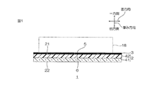
- FIG. 1 is a schematic view showing an embodiment of the transparent conductive layer and the transparent conductive sheet of the present invention.
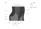
- FIG. 2 shows a cross-sectional view of the transparent conductive layer in the transparent conductive sheet shown in FIG.
- FIG. 3 is a schematic view showing an embodiment of a method for manufacturing a transparent conductive layer and a transparent conductive sheet of the present invention.
- FIG. 3A shows a step of preparing a transparent base material in the first step.
- FIG. 3B shows a step of arranging the hard coat layer on one surface in the thickness direction of the transparent base material in the first step.
- FIG. 3C shows a second step of arranging the transparent conductive layer on one surface in the thickness direction of the base material layer.
- FIG. 3D shows a third step of heating the transparent conductive layer.
- FIG. 3A shows a step of preparing a transparent base material in the first step.
- FIG. 3B shows a step of arranging the hard coat layer on one surface in the thickness direction of the transparent base material
- FIG. 4 is a graph showing the relationship between the specific resistance of the amorphous transparent conductive layer and the amount of oxygen introduced.
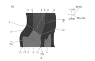
- FIG. 5 shows a schematic view of a modified example of the transparent conductive layer of the present invention (a modified example in which the second grain boundary does not have an apex).
- FIG. 6 shows a schematic view of a modified example of the transparent conductive layer of the present invention (a modified example having a plurality of second grain boundaries arranged in the thickness direction).
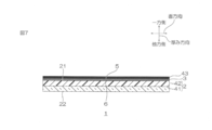
- FIG. 7 shows a schematic view of a modified example of the transparent conductive sheet of the present invention (a modified example including a first rare gas atom-free transparent conductive layer).
- FIG. 2 An embodiment of the transparent conductive layer and the transparent conductive sheet of the present invention will be described with reference to FIGS. 1 and 2.
- a plurality of crystal grains 4 (described later) are clearly shown, and the first grain boundary 7 (described later) and the second grain boundary 8 (described later), and the leader line and the virtual line segment (chain line) are shown.
- a plurality of crystal grains 4 are drawn in grays having different densities.
- the transparent conductive sheet 1 has a predetermined thickness and has a sheet shape extending in a plane direction orthogonal to the thickness direction.
- the transparent conductive sheet 1 includes a base material layer 2 and a transparent conductive layer 3 in order toward one side in the thickness direction.
- the transparent conductive sheet 1 includes a base material layer 2 and a transparent conductive layer 3 arranged on one surface of the base material layer 2 in the thickness direction.
- the base material layer 2 is a transparent base material for ensuring the mechanical strength of the transparent conductive sheet 1.
- the base material layer 2 extends in the plane direction.
- the base material layer 2 has a base material first main surface 21 and a base material second main surface 22.
- the first main surface 21 of the base material is a flat surface.
- the base material second main surface 22 is arranged to face the base material first main surface 21 on the other side in the thickness direction at intervals.
- the base material layer 2 is located on the second main surface 6 (described later) side of the transparent conductive layer 3.
- the base material second main surface 22 is parallel to the base material first main surface 21.
- the flat surface may be a plane in which the first main surface 21 of the base material layer 2 and the second main surface 22 of the base material layer 2 are substantially parallel to each other. For example, fine irregularities and waviness that cannot be observed are allowed.
- the base material layer 2 includes a transparent base material 41 and a functional layer 42.
- the base material layer 2 includes a transparent base material 41 and a functional layer 42 in order toward one side in the thickness direction.
- the base material layer 2 includes a transparent base material 41 and a functional layer 42 arranged on one surface in the thickness direction of the transparent base material 41.
- the transparent base material 41 has a film shape.
- Examples of the material of the transparent base material 41 include olefin resin, polyester resin, (meth) acrylic resin (acrylic resin and / or methacrylic resin), polycarbonate resin, polyether sulfone resin, polyarylate resin, melamine resin, and polyamide resin. Examples thereof include a polyimide resin, a cellulose resin, and a polystyrene resin.
- Examples of the olefin resin include polyethylene, polypropylene, and cycloolefin polymers.
- Examples of the polyester resin include polyethylene terephthalate (PET), polybutylene terephthalate, and polyethylene naphthalate.
- Examples of the (meth) acrylic resin include polymethacrylate.
- polyester resin is preferable, and polyethylene terephthalate (PET) is more preferable, from the viewpoint of transparency and moisture permeation resistance.
- the transparent base material 41 has transparency. Specifically, the total light transmittance (JIS K 7375-2008) of the transparent base material 41 is, for example, 60% or more, preferably 80% or more, and more preferably 85% or more.
- the thickness of the transparent substrate 41 is, for example, 1 ⁇ m or more, preferably 10 ⁇ m or more, preferably 30 ⁇ m or more, and for example, 1000 ⁇ m or less, preferably 500 ⁇ m or less, more preferably 250 ⁇ m or less, still more preferably 200 ⁇ m.
- it is particularly preferably 100 ⁇ m or less, and most preferably 60 ⁇ m or less.
- the functional layer 42 is arranged on one side of the transparent base material 41 in the thickness direction.
- the functional layer 42 has a film shape.
- Examples of the functional layer 42 include a hard coat layer.
- the base material layer 2 includes the transparent base material 41 and the hard coat layer in order toward one side in the thickness direction.
- the functional layer 42 is a hard coat layer
- the hard coat layer is a protective layer for suppressing scratches on the transparent conductive sheet 1.
- the hard coat layer is formed from, for example, a hard coat composition.
- the hard coat composition contains a resin and, if necessary, particles. That is, the hard coat layer contains a resin and, if necessary, particles.
- thermoplastic resin examples include polyolefin resins.
- the curable resin examples include an active energy ray-curable resin that is cured by irradiation with active energy rays (for example, ultraviolet rays and electron beams) and a thermosetting resin that is cured by heating.
- the curable resin preferably includes an active energy ray-curable resin.
- the active energy ray-curable resin examples include (meth) acrylic ultraviolet curable resin, urethane resin, melamine resin, alkyd resin, siloxane-based polymer, and organic silane condensate.
- the active energy ray-curable resin is preferably a (meth) acrylic ultraviolet-curable resin.
- the resin can contain, for example, the reactive diluent described in JP-A-2008-88309. Specifically, the resin can include polyfunctional (meth) acrylates.
- the resin can be used alone or in combination of two or more.
- Examples of particles include metal oxide fine particles and organic fine particles.
- Examples of the material of the metal oxide fine particles include silica, alumina, titania, zirconia, calcium oxide, tin oxide, indium oxide, cadmium oxide, and antimony oxide.
- Examples of the material of the organic fine particles include polymethylmethacrylate, silicone, polystyrene, polyurethane, acrylic-styrene copolymer, benzoguanamine, melamine, and polycarbonate.
- Particles can be used alone or in combination of two or more.
- a thixotropy-imparting agent a photopolymerization initiator, a filler (for example, organic clay), and a leveling agent can be added to the hard coat composition in an appropriate ratio.
- the hard coat composition can be diluted with a known solvent.
- a diluted solution of the hard coat composition is applied to one surface of the transparent base material 41 in the thickness direction in detail, and if necessary, it is heated and dried. After drying, the hard coat composition is cured by, for example, irradiation with active energy rays.
- the thickness of the hard coat layer is, for example, 0.1 ⁇ m or more, preferably 0.5 ⁇ m or more, more preferably 1 ⁇ m or more, and for example, 20 ⁇ m or less, preferably 10 ⁇ m or less, more preferably 5 ⁇ m or less. ..
- the transparent conductive layer 3 is arranged on one side of the base material layer 2 in the thickness direction. Specifically, the transparent conductive layer 3 is in contact with the entire surface of the first main surface 21 of the base material of the base material layer 2.
- the transparent conductive layer 3 has a predetermined thickness, preferably includes a region that is a single layer extending in the plane direction orthogonal to the thickness direction, and more preferably a single layer extending in the plane direction orthogonal to the thickness direction. It is a layer.
- the transparent conductive layer 3 includes a region which is not a plurality of layers laminated in the thickness direction, and more preferably, the transparent conductive layer 3 is not a plurality of layers laminated in the thickness direction. ..
- the plurality of transparent conductive layers partitioned along the plane direction, wherein the plurality of transparent conductive layers including a boundary parallel to the first main surface 21 of the base material layer 2 are the transparent conductive layers of the present invention. It is preferable that it is not included.
- the transparent conductive layer 3 includes a first main surface 5 and a second main surface 6 facing each other in the thickness direction.
- the first main surface 5 is exposed on one side in the thickness direction.
- the first main surface 5 is a flat surface.
- the second main surface 6 is arranged to face the other side of the first main surface 5 in the thickness direction at intervals.
- the second main surface 6 is a flat surface parallel to the first main surface 21. In this one embodiment, the second main surface 6 comes into contact with the first main surface 21 of the base material.
- the flat surface does not matter whether the first main surface 5 and the second main surface 6 are substantially parallel planes. For example, fine irregularities and waviness that cannot be observed are allowed.
- the transparent conductive layer 3 is crystalline.
- the transparent conductive layer 3 does not include an amorphous region in the plane direction, but includes only a crystalline region.
- the transparent conductive layer containing the amorphous region is identified, for example, by observing the crystal grains in the plane direction of the transparent conductive layer with TEM.
- the transparent conductive layer 3 is crystalline, for example, the transparent conductive layer 3 is immersed in a 5% by mass hydrochloric acid aqueous solution for 15 minutes, washed with water and dried, and the first main surface 5 has a length of about 15 mm. The resistance between the two terminals is measured, and the resistance between the two terminals is 10 k ⁇ or less. On the other hand, if the resistance between the two terminals exceeds 10 k ⁇ , the transparent conductive layer 3 is amorphous.
- the transparent conductive layer 3 has a plurality of crystal grains 4. Crystal grains 4 are sometimes referred to as grains.
- the transparent conductive layer 3 has a first grain boundary 7 and a second grain boundary 8 that partition a plurality of crystal grains 4.
- the first grain boundary 7 extends in the thickness direction, and in a cross-sectional view, one end edge 9 and the other end edge 10 in the thickness direction are opened on each of the first main surface 5 and the second main surface 6.
- a plurality of first grain boundaries 7 are present at intervals in the plane direction.
- the first grain boundary 7 can include a curved portion 15, a bent portion 16, and the like in a cross-sectional view.
- the second grain boundary 8 branches from the first intermediate portion 11 in the thickness direction of one first grain boundary 7 (see reference numeral 7A) among the plurality of first grain boundaries 7, and becomes one first grain boundary 7. It reaches the second intermediate portion 12 in the thickness direction of another adjacent first grain boundary 7 (see reference numeral 7B).
- the first intermediate portion 11 and the second intermediate portion 12 are, for example, both bent portions 16.
- the second grain boundary 8 connects the first intermediate portion 11 and the second intermediate portion 12.
- the second grain boundary 8 partitions the first crystal grain 31 located on one side in the thickness direction and the second crystal grain 32 located on the other side in the thickness direction in the thickness direction. That is, the first crystal grain 31 and the second crystal grain 32 are sequentially arranged in the thickness direction by the second grain boundary 8.
- the first crystal grain 31 includes the first main surface 5.
- the second crystal grain 32 includes the second main surface 6.
- the second grain boundary 8 includes the second curved portion 17.
- the second curved portion 17 has one vertex 20. That is, the second grain boundary 8 has a vertex 20.
- the apex 20 is located at a position 5 nm or more away from the line segment (broken line) connecting the first intermediate portion 11 and the second intermediate portion 12 in the cross-sectional view.
- the above-mentioned distance is preferably 10 nm or more.
- the apex 20 is located on one side in the thickness direction with respect to the above-mentioned line segment.
- the second grain boundary 8 has the above-mentioned apex 20
- the water path (described later) from the first main surface 5 to the second main surface 6 can be further lengthened. As a result, the moisture permeation resistance can be further improved.
- first grain boundary 7A extends from one end edge 9 in the thickness direction of the first grain boundary 7A to the first intermediate portion 11, branches from the first intermediate portion 11 to the second grain boundary 8, and from the second intermediate portion 12 to the other first.
- the grain boundaries that reach the grain boundaries 7B and subsequently reach the other end edge 10 in the thickness direction are not the first grain boundaries of the present invention. That is, the grain boundary from one first grain boundary 7A to another grain boundary 7B via the second grain boundary 8 is not the first grain boundary of the present invention.
- one of the first grain boundaries 7 extends from one end edge 9 in the thickness direction to the first intermediate portion 11 and branches from the first intermediate portion 11 into a plurality of each of the plurality of first grain boundaries 7.
- the grain boundary reaching the other end edge 10 in the thickness direction is included in the first grain boundary of the present invention. That is, the first grain boundary 7 that does not pass through the second grain boundary 8 is included in the first grain boundary of the present invention.
- the first grain boundary 7 and the second grain boundary 8 can be formed by, for example, adjusting the temperature of the base material layer 2 during sputtering, the film formation pressure, and the magnetic field strength of the target surface.
- the transparent conductive layer 3 contains a material and a rare gas atom having an atomic number larger than that of a trace amount of argon atom (hereinafter, referred to as a first rare gas atom). Specifically, in the transparent conductive layer 3, a trace amount of the first rare gas atom is present in the material matrix.
- the material is not particularly limited.
- the material for example, at least one selected from the group consisting of In, Sn, Zn, Ga, Sb, Nb, Ti, Si, Zr, Mg, Al, Au, Ag, Cu, Pd, and W.
- Examples include metal oxides including metals.
- examples of the metal oxide include tin-containing oxide, indium zinc composite oxide (IZO), indium gallium zinc composite oxide (IGZO), and indium gallium composite oxide (IGO).
- examples of the tin-containing oxide include indium tin oxide composite oxide (ITO) and antimony tin composite oxide (ATO).
- the metal oxide preferably includes a tin-containing oxide. If the material is a tin-containing oxide, it has excellent transparency and electrical conductivity.
- the content of tin oxide (SnO 2 ) in the transparent conductive layer 3 (tin-containing oxide) is not particularly limited, and is, for example, 0.5% by mass or more, preferably 3% by mass or more, and more preferably 6% by mass. % Or more, and for example, less than 50% by mass, preferably 25% by mass or less, more preferably 15% by mass or less.
- Examples of the first rare gas atom include a krypton atom and a xenon atom, and preferably a krypton atom.
- the first rare gas atom is derived from the first rare gas as a sputtering gas described later.
- the first rare gas atom derived from the first rare gas (described later) as the sputtering gas is incorporated into the transparent conductive layer 3.
- the content of the first rare gas atom in the transparent conductive layer 3 is, for example, 1.0 atom% or less, more preferably 0.7 atom% or less, still more preferably 0.5 atom% or less, and particularly preferably. It is 0.3 atomic% or less, most preferably 0.2 atomic% or less, further less than 0.1 atomic%, and for example, 0.0001 atomic% or more.
- the content of the first noble gas atom can be measured by, for example, Rutherford backscatter spectroscopy. Further, the presence of the first noble gas atom can be confirmed by, for example, fluorescent X-ray analysis.
- the content of the first noble gas atom in the transparent conductive layer 3 is excessively small (specifically, when the content of the first noble gas atom is not equal to or higher than the detection limit value (lower limit value) of the Rutherford backscattering analysis). ), The content of the first noble gas atom may not be quantified by Rutherford backscattering analysis. However, in the present application, even in such a case, when the presence of the first noble gas atom is identified by fluorescent X-ray analysis, the content of the first noble gas atom is at least 0.0001. Judge that it is atomic% or more.
- the thickness of the transparent conductive layer 3 is, for example, 10 nm or more, preferably 30 nm or more, more preferably 70 nm or more, still more preferably 100 nm or more, particularly preferably 120 nm or more, most preferably from the viewpoint of moisture permeability. From the viewpoint of thinning, for example, 1000 nm or less, preferably 500 nm or less, more preferably less than 300 nm, still more preferably 200 nm or less, particularly preferably less than 150 nm, most preferably 148 nm or less. Is. How to determine the thickness of the transparent conductive layer 3 will be described in detail later in Examples.
- the ratio of the average of the distances of the one end edge 9 and the other end edge 10 of the first grain boundary 7 in the thickness direction to the thickness of the transparent conductive layer 3 is, for example, more than 1, preferably 1.1 or more, more preferably. Is 1.2 or more, more preferably 1.5 or more, and for example, 5 or less, preferably 2.5 or less. Further, in a cross-sectional view, the average of the distances of the first intermediate portion 11 and the second intermediate portion 12 of the second grain boundary 8 with respect to the average of the distances of the one end edge 9 and the other end edge 10 of the first grain boundary 7 in the thickness direction.
- the ratio is, for example, 0.1 or more, preferably 0.3 or more, and for example, 5 or less, preferably 3 or less. If the above ratio exceeds the above lower limit and falls below the above upper limit, the moisture permeation resistance of the transparent conductive layer 3 can be improved.
- the moisture permeability for example, a 0 [g / m 2 ⁇ 24h ] exceeded.
- the transparent conductive layer 3 is excellent in moisture permeability.
- the moisture permeability of the transparent conductive layer 3 will be described in the evaluation method of Examples described later.
- the surface resistance of the transparent conductive layer 3 is, for example, 200 ⁇ / ⁇ or less, preferably 50 ⁇ / ⁇ or less, more preferably 30 ⁇ / ⁇ or less, still more preferably 20 ⁇ / ⁇ or less, and particularly preferably 15 ⁇ / ⁇ or less. And, for example, it exceeds 0 ⁇ / ⁇ .
- the specific resistance value of the transparent conductive layer 3 is, for example, 2.2 ⁇ 10-4 ⁇ cm or less, preferably 1.8 ⁇ 10-4 ⁇ cm or less, and more preferably 1.0 ⁇ 10-4 ⁇ cm or less. ..
- the specific resistance value is, for example, 0.1 ⁇ 10 -4 ⁇ ⁇ cm or more, preferably 0.5 ⁇ 10 -4 ⁇ ⁇ cm or more, more preferably 1.0 ⁇ 10 -4 ⁇ ⁇ cm. It is cm or more, more preferably 1.01 ⁇ 10 -4 ⁇ ⁇ cm or more.
- the specific resistance value can be obtained by multiplying the thickness of the transparent conductive layer 3 and the value of the surface resistance.
- the method for manufacturing the transparent conductive layer 3 and the transparent conductive sheet 1 includes a first step of preparing the base material layer 2 and a second step of arranging the transparent conductive layer 3 on one surface of the base material layer 2 in the thickness direction. It includes a third step of heating the transparent conductive layer 3. Further, in this manufacturing method, each layer is arranged in order by, for example, a roll-to-roll method.
- the base material layer 2 is prepared.
- a diluted solution of the hard coat composition is applied to one surface in the thickness direction of the transparent base material 41, and after drying, the hard coat composition is cured by ultraviolet irradiation or heating. As a result, a hard coat layer (functional layer 42) is formed on one surface of the transparent base material 41 in the thickness direction. As a result, the base material layer 2 is prepared.
- ⁇ Second step> In the second step, as shown in FIG. 3C, the transparent conductive layer 3 is arranged on one surface of the base material layer 2 in the thickness direction.
- sputtering is performed in the presence of sputtering gas while facing one surface of the base material layer 2 in the thickness direction to a target made of the material of the transparent conductive layer 3. Further, in sputtering, the base material layer 2 is in close contact with each other along the circumferential direction of the film forming roll.
- a reactive gas for example, oxygen
- oxygen may be present in addition to the sputtering gas.
- the sputtering gas is a rare gas having an atomic number larger than that of the argon atom (hereinafter referred to as the first rare gas).
- the first rare gas include krypton gas and xenon gas, and preferably krypton gas.
- the partial pressure of the sputtering gas in the sputtering apparatus is, for example, 0.05 Pa or more, preferably 0.1 Pa or more, and for example, 10 Pa or less, preferably 5 Pa or less, more preferably 1 Pa or less.
- the amount of the reactive gas introduced can be estimated from the surface resistance of the amorphous transparent conductive layer 3.
- the film quality (surface resistance) of the amorphous transparent conductive layer 3 changes depending on the amount of the reactive gas introduced into the amorphous transparent conductive layer 3, so that the target amorphous transparent conductive layer 3 is desired.
- the amount of the reactive gas introduced can be adjusted according to the surface resistance of the transparent conductive layer 3.
- the amount of the reactive gas introduced is adjusted in the range X of the region X of FIG. 4, and the amorphous transparent is transparent. It is preferable to obtain the conductive layer 3.
- the specific resistance of the amorphous transparent conductive layer 3 is, for example, 8.0 ⁇ 10 -4 ⁇ ⁇ cm or less, preferably 7.0 ⁇ 10 -4 ⁇ ⁇ cm or less, or, for example. , 2.0 ⁇ 10 -4 ⁇ ⁇ cm, preferably 4.0 ⁇ 10 -4 ⁇ ⁇ cm or more, more preferably 5.0 ⁇ 10 -4 ⁇ ⁇ cm or more. Introduce.
- the pressure in the sputtering apparatus is substantially the total pressure of the partial pressure of the sputtering gas and the partial pressure of the reactive gas.
- the power supply may be, for example, any of a DC power supply, an AC power supply, an MF power supply, and an RF power supply. Moreover, these combinations may be used.
- the value of the discharge output with respect to the long side of the target is, for example, 0.1 W / mm or more, preferably 0.5 W / mm, more preferably 1 W / mm or more, still more preferably 5 W / mm or more, or, for example. , 30 W / mm or less, preferably 15 W / mm or less.
- the long side direction of the target is, for example, a direction (TD direction) orthogonal to the transport direction in the roll-to-roll type sputtering apparatus.
- the horizontal magnetic field strength on the target surface is, for example, 10 mT or more, preferably 60 mT or more, and for example, 300 mT or less.
- the material of the transparent conductive layer 3 ejected from the target by sputtering is applied to the base material layer 2.
- the transparent conductive layer 3 is cooled through the cooling of the base material layer 2 by the film forming roll to crystallize the transparent conductive layer 3. Suppress.
- the temperature of the film-forming roll (and thus the temperature of the substrate layer 2) is, for example, ⁇ 50 ° C. or higher, preferably ⁇ 20 ° C. or higher, more preferably ⁇ 10 ° C. or higher, and for example. It is 30 ° C. or lower, preferably 20 ° C. or lower, more preferably 15 ° C. or lower, still more preferably 10 ° C. or lower, and particularly preferably 5 ° C. or lower.
- the base material layer 2 can be sufficiently cooled, and crystal growth during film formation of the transparent conductive layer 3 (particularly, crystal growth in the thickness direction of the transparent conductive layer 3) can be suppressed.
- the transparent conductive layer 3 after passing through the above the first grain boundary 7 and the second grain boundary 8 can be easily obtained.
- the amorphous transparent conductive layer 3 is arranged on one surface of the base material layer 2 in the thickness direction.
- the first rare gas is used as the sputtering gas, the first rare gas atom derived from the first rare gas is taken into the transparent conductive layer 3.
- the amorphous transparent conductive layer 3 is heated.
- the amorphous transparent conductive layer 3 is heated by a heating device (for example, an infrared heater and a hot air oven).
- the heating temperature is, for example, 80 ° C. or higher, preferably 110 ° C. or higher, and for example, less than 200 ° C., preferably 180 ° C. or lower.
- the heating time is, for example, 1 minute or more, preferably 10 minutes or more, more preferably 30 minutes or more, and for example, 24 hours or less, preferably 4 hours or less, more preferably 2 hours or less. be.
- the amorphous transparent conductive layer 3 is crystallized, and the crystalline transparent conductive layer 3 is formed.
- the transparent conductive layer 3 can be obtained, and the transparent conductive sheet 1 including the base material layer 2 and the transparent conductive layer 3 in this order can be obtained.
- the transparent conductive layer 3 can be patterned. Patterning is performed, for example, by etching.
- the transparent conductive layer 3 has a pattern shape.
- the pattern shape can be freely designed.
- the article with the transparent conductive sheet is provided with the parts and the transparent conductive sheet 1 in order toward one side in the thickness direction.
- the article with the transparent conductive sheet includes parts, a base material layer 2, and a transparent conductive layer 3 in this order toward one side in the thickness direction.
- the article is not particularly limited, and examples thereof include elements, members, and devices. More specifically, examples of the element include a dimming element and a photoelectric conversion element. Examples of the dimming element include a current-driven dimming element and an electric field-driven dimming element. Examples of the current-driven dimming element include an electrochromic (EC) dimming element. Examples of the electric field drive type dimming element include a PDLC (polymer dispensed liquid crystal) dimming element, a PNLC (polymer network liquid crystal) dimming element, and an SPD (suspended liquid crystal) dimming element. Examples of the photoelectric conversion element include a solar cell.
- Examples of the solar cell include an organic thin film solar cell, a perovskite solar cell, and a dye-sensitized solar cell.
- Examples of the member include an electromagnetic wave shield member, a heat ray control member, a heater member, lighting, and an antenna member.
- Examples of the device include a touch sensor device and an image display device.
- the article with a transparent conductive sheet can be obtained, for example, by adhering a component and a base material layer 2 in the transparent conductive sheet 1 via a fixing functional layer.
- Examples of the fixing functional layer include an adhesive layer and an adhesive layer.
- the fixing functional layer any material having transparency can be used without particular limitation.
- the fixing functional layer is preferably formed of a resin.
- the resin include acrylic resin, silicone resin, polyester resin, polyurethane resin, polyamide resin, polyvinyl ether resin, vinyl acetate / vinyl chloride copolymer, modified polyolefin resin, epoxy resin, fluororesin, natural rubber, and synthetic rubber.
- an acrylic resin is preferably selected as the resin from the viewpoint of excellent optical transparency, exhibiting adhesive properties such as appropriate wettability, cohesiveness and adhesiveness, and excellent weather resistance and heat resistance.
- NS adhesive properties
- the fixing functional layer (resin forming the fixing functional layer) is disclosed in a known corrosion inhibitor and a migration inhibitor (for example, Japanese Patent Application Laid-Open No. 2015-0222397) in order to suppress corrosion and migration of the transparent conductive layer 3. Material) can also be added.
- a known ultraviolet absorber may be added to the fixing functional layer (resin forming the fixing functional layer) in order to suppress deterioration of the article with a transparent conductive sheet during outdoor use.
- the ultraviolet absorber include benzophenone compounds, benzotriazole compounds, salicylic acid compounds, oxalic acid anilides compounds, cyanoacrylate compounds, and triazine compounds.
- cover layer can be arranged on the upper surface of the transparent conductive layer 3 in the article with the transparent conductive sheet.
- the cover layer is a layer that covers the transparent conductive layer 3, and can improve the reliability of the transparent conductive layer 3 and suppress functional deterioration due to scratches.
- the cover layer is preferably a dielectric.
- the cover layer is formed from a mixture of resin and inorganic materials.
- the resin include the resin exemplified by the fixing functional layer.
- the inorganic material has a composition containing, for example, an inorganic oxide such as silicon oxide, titanium oxide, niobium oxide, aluminum oxide, zirconium dioxide and calcium oxide, and a fluoride such as magnesium fluoride.
- a corrosion inhibitor, a migration inhibitor, and an ultraviolet absorber can be added to the cover layer (mixture of resin and inorganic material) from the same viewpoint as the above-mentioned fixing functional layer.
- an article with a transparent conductive sheet can also be obtained by adhering the component and the transparent conductive layer 3 in the transparent conductive sheet 1 via the fixing functional layer.
- the transparent conductive layer 3 can be arranged on one side in the thickness direction of the component to obtain an article with the transparent conductive layer.
- the article with a transparent conductive layer is provided with a component and a transparent conductive layer 3 in order toward one side in the thickness direction.
- the transparent conductive layer 3 is arranged on one surface in the thickness direction of the component by a sputtering method, or the transparent conductive layer 3 is transferred from the transparent conductive sheet 1 to one surface in the thickness direction of the component. Obtained by
- the component and the transparent conductive layer 3 can be adhered to each other via the fixing function layer.
- cover layer can be arranged on the upper surface of the transparent conductive layer 3 in the article with the transparent conductive layer.
- the transparent conductive layer 3 has a second grain boundary 8 that branches from the first intermediate portion 11 of one first grain boundary 7A and reaches the second intermediate portion 12 of the other first grain boundary 7B. Therefore, even if water comes into contact with the first main surface 5, it is possible to secure a long water path from the first main surface 5 to the second main surface 6. As a result, the transparent conductive layer 3 is excellent in moisture permeation resistance. Further, the transparent conductive sheet 1 provided with the transparent conductive layer 3 is also excellent in moisture permeation resistance.
- the transparent conductive sheet 1 when used as an electrode of a light control element or a solar cell element, even if the second main surface 22 of the base material is exposed to the outside air containing water, the transparent conductive layer 3 has a second grain boundary. Since the number 8 is provided, the intrusion route of water from the first main surface 5 to the second main surface 6 becomes long, and the arrival of water at the first main surface 5 can be delayed. Therefore, damage to the dimming layer or cell 18 (see FIG. 1) due to the ingress of water can be delayed. That is, a dimming element or a solar cell element having excellent moisture resistance can be configured.
- the transparent conductive layer 3 has the first grain boundary 7 and the second grain boundary 8, the specific resistance tends to be high from the viewpoint of carrier mobility.
- the transparent conductive layer 3 contains an atom derived from the sputtering gas (first rare gas atom). Therefore, even if the transparent conductive layer 3 has the first grain boundary 7 and the second grain boundary 8, the specific resistance of the transparent conductive layer 3 can be lowered.
- the transparent conductive layer 3 is manufactured by the sputtering method, atoms derived from the sputtering gas are incorporated into the transparent conductive layer 3. Atoms derived from such a sputtering gas inhibit the crystallization of the transparent conductive layer 3. As a result, the specific resistance of the transparent conductive layer 3 increases.
- the transparent conductive layer 3 is obtained by using the first rare gas as the sputtering gas. Since the first rare gas has an atomic weight larger than that of argon, it is possible to suppress the incorporation of atoms derived from the first rare gas (first rare gas atom) into the transparent conductive layer 3. That is, although the transparent conductive layer 3 contains an atom derived from the first rare gas (first rare gas atom), the amount thereof is suppressed as described above. Therefore, it is possible to prevent the first rare gas atom from inhibiting the crystallization of the transparent conductive layer 3. As a result, the specific resistance of the transparent conductive layer 3 can be lowered.
- the transparent conductive layer 3 can have a low specific resistance and is also excellent in moisture permeation resistance.
- the transparent conductive sheet 1, the touch sensor, the dimming element, the photoelectric conversion element, the heat ray control member, the antenna, the electromagnetic wave shielding member, and the image display device provided with the transparent conductive layer 3 have low resistance and have low resistance. Has excellent moisture permeability.
- the apex 20 may be located on the other side in the thickness direction from the line segment shown by the broken line.
- the second grain boundary 8 does not have to have a vertex 20.
- the second grain boundary 8 has a vertex 20.
- the path of water via the second grain boundary 8 having the apex 20 can be further lengthened. Therefore, the moisture permeation resistance of the transparent conductive layer 3 is even more excellent.
- the transparent conductive layer 3 includes a plurality of second grain boundaries 8 that overlap each other when projected in the thickness direction.
- the first grain boundary 7 may include a non-contact first grain boundary 7C that does not come into contact with the second grain boundary 8 in cross-sectional view.
- the transparent conductive sheet 1 includes the base material layer 2 and the transparent conductive layer 3 in order toward one side in the thickness direction. Further, in such a transparent conductive sheet 1, the transparent conductive layer 3 contains a first rare gas atom.
- the transparent conductive sheet 1 may further include a transparent conductive layer containing no first rare gas atom (hereinafter, referred to as a first rare gas atom-free transparent conductive layer 43).
- a transparent conductive layer containing no first rare gas atom hereinafter, referred to as a first rare gas atom-free transparent conductive layer 43.
- the transparent conductive sheet 1 the base material layer 2, the transparent conductive layer 3, and the first rare gas atom-free transparent conductive layer 43 are directed to one side in the thickness direction.
- the transparent conductive sheet 1 is arranged on the base material layer 2, the transparent conductive layer 3 arranged on one side in the thickness direction of the base material layer 2, and the transparent conductive layer 3 on one side in the thickness direction.
- the first rare gas atom-free transparent conductive layer 43 is provided.
- the first rare gas atom-free transparent conductive layer 43 does not contain the first rare gas atom, and has the above-mentioned material (specifically, the same material as the material contained in the transparent conductive layer 3) and an atomic number of a trace amount of argon atom or less.
- a noble gas atom having a hereinafter referred to as a second rare gas atom.
- a trace amount of the second rare gas atom is present in the material matrix.
- Examples of the second rare gas atom include an argon atom, a neon atom, and a helium atom, and preferably an argon atom.
- the second noble gas atom is derived from the second noble gas as a sputtering gas described later.
- the second rare gas atom derived from the second rare gas (described later) as the sputtering gas is incorporated into the first rare gas atom-free transparent conductive layer 43.
- the content of the second rare gas atom in the transparent conductive layer 3 is larger than the content of the first rare gas atom. Therefore, the content of the second rare gas atom in the first rare gas atom-free transparent conductive layer 43 is, specifically, 2.0 atom% or less, preferably 1.0 atom% or less, more preferably 1.0 atom% or less. 0.7 atomic% or less, particularly preferably 0.5 atomic% or less, most preferably 0.3 atomic% or less, further 0.2 atomic% or less, and for example, 0.0001 atomic% or more. be.
- the method for confirming the content of the second rare gas atom and the method for confirming the presence of the second rare gas atom are the above-mentioned method for confirming the content of the first rare gas atom and the method for confirming the presence of the first rare gas atom. It is the same as the confirmation method.
- the thickness of the first rare gas atom-free transparent conductive layer 43 is, for example, 1 nm or more, preferably 10 nm or more, more preferably 30 nm or more, still more preferably 70 nm or more, and for example, 500 nm or less, preferably. It is less than 300 nm, more preferably 200 nm or less, still more preferably less than 150 nm, and particularly preferably 100 nm or less.
- the method of obtaining the thickness of the first rare gas atom-free transparent conductive layer 43 is the same as the method of obtaining the thickness of the transparent conductive layer 3.
- the transparent conductive layer 3 is placed on one surface in the thickness direction of the base material layer 2. Is arranged, the first rare gas atom-free transparent conductive layer 43 is arranged on one surface of the transparent conductive layer 3 in the thickness direction.
- sputtering is performed in the presence of sputtering gas while facing one side of the transparent conductive layer 3 in the thickness direction to a target made of the material of the first rare gas atom-free transparent conductive layer 43.
- the transparent conductive layer 3 (specifically, the base material layer 2 provided with the transparent conductive layer 3) is in close contact with each other along the circumferential direction of the film forming roll.
- a reactive gas for example, oxygen
- oxygen may be present in addition to the sputtering gas.
- the sputtering gas is a rare gas having an atomic number equal to or less than an argon atom (hereinafter referred to as a second rare gas).
- a second rare gas examples include argon gas, neon gas, and helium gas, and preferably argon gas.
- the partial pressure of the sputtering gas, the amount of the reactive gas introduced, the power source, and the value of the discharge output with respect to the long side of the target in the sputtering apparatus are the same as the sputtering conditions when the transparent conductive layer 3 is arranged.
- the material of the first rare gas atom-free transparent conductive layer 43 ejected from the target by sputtering is formed on the transparent conductive layer 3.
- the first rare gas atom-free transparent conductive layer 43 is formed by cooling the transparent conductive layer 3 with a film forming roll. It is cooled to suppress the crystallization of the first rare gas atom-free transparent conductive layer 43.
- the temperature of the film-forming roll is the same as the temperature of the film-forming roll in sputtering when the transparent conductive layer 3 is arranged.
- the amorphous first rare gas atom-free transparent conductive layer 43 is arranged on one surface of the transparent conductive layer 3 in the thickness direction.
- the second rare gas is used as the sputtering gas, the second rare gas atom derived from the second rare gas is taken into the first rare gas atom-free transparent conductive layer 43.
- the first rare gas atom-free transparent conductive layer 43 is obtained, and the transparent conductive sheet including the base material layer 2, the transparent conductive layer 3, and the first rare gas atom-free transparent conductive layer 43 in this order. 1 is obtained.
- the transparent conductive sheet 1 includes a base material layer 2, a transparent conductive layer 3, and a first rare gas atom-free transparent conductive layer 43 in order toward one side in the thickness direction.
- the transparent conductive sheet 1 may be provided with the base material layer 2, the first rare gas atom-free transparent conductive layer 43, and the transparent conductive layer 3 in order toward one side in the thickness direction. ..
- the functional layer 42 is a hard coat layer has been described, but the functional layer 42 may be an optical adjustment layer.
- the optical adjustment layer is transparent in order to ensure excellent transparency of the transparent conductive sheet 1 while suppressing the pattern visibility of the transparent conductive layer 3 and suppressing reflection at the interface in the transparent conductive sheet 1.
- This is a layer for adjusting the optical physical characteristics (for example, the refractive index) of the conductive sheet 1.
- the optical adjustment layer is formed from, for example, an optical adjustment composition.
- the optical adjustment composition contains, for example, a resin and particles.
- the resin include the resins mentioned in the above hard coat composition.
- the particles include the particles mentioned in the above-mentioned hard coat composition.
- the optical adjustment composition may be a simple substance of a resin or a simple substance of an inorganic substance.
- the resin include the resins mentioned in the above hard coat composition.
- the inorganic substance include semi-metal oxides and / or metal oxides such as silicon oxide, alumina, titania, zirconia, calcium oxide, tin oxide, indium oxide, cadmium oxide and antimony oxide. It does not matter whether the metalloid oxide and / or the metal oxide has a chemical composition.
- the thickness of the optical adjustment layer is, for example, 1 nm or more, preferably 5 nm or more, more preferably 10 nm or more, and for example, 200 nm or less, preferably 100 nm or less.
- the thickness of the optical adjustment layer can be calculated, for example, based on the wavelength of the interference spectrum observed using an instantaneous multi-photometric system. Further, the thickness may be specified by observing the cross section of the optical adjustment layer with an FE-TEM.
- a hard coat layer and an optical adjustment layer can be used together (a multilayer including the hard coat layer and the optical adjustment layer).
- the base material layer 2 includes the transparent base material 41 and the functional layer 42 in order toward one side in the thickness direction.
- the base material layer 2 does not include the functional layer 42 and may be made of the transparent base material 41.
- the transparent conductive layer 3 contains a material and a first rare gas atom, but the transparent conductive layer 3 may also contain a second rare gas atom.
- the transparent conductive layer 3 contains a second rare gas atom
- a second rare gas is used together with the first rare gas as the sputtering gas in the second step.
- the second rare gas atom derived from the second rare gas is taken into the transparent conductive layer 3 together with the first rare gas atom derived from the first rare gas.
- the content of the second rare gas atom is 2.0 atom% or less, preferably 1.0 atom% or less, more preferably 0.7 atom% or less, and particularly preferably 0.5. It is atomic% or less, most preferably 0.3 atomic% or less, further 0.2 atomic% or less, and for example, 0.0001 atomic% or more.
- the transparent conductive layer 3 can contain the second rare gas atom, but preferably, the transparent conductive layer 3 does not contain the second rare gas atom. That is, preferably, the transparent conductive layer 3 is composed of a material and a first noble gas atom.
- amorphous transparent conductive layer having a thickness of 103 nm was arranged on one surface of the base material layer (hard coat layer) in the thickness direction by a reactive sputtering method.
- a reactive sputtering method a sputtering film forming apparatus (DC magnetron sputtering apparatus) capable of carrying out a film forming process by a roll-to-roll method was used.
- a sintered body of indium oxide and tin oxide (tin oxide concentration was 10% by mass) was used as a target.
- a DC power supply was used as the power supply for applying the voltage to the target.
- the horizontal magnetic field strength on the target was 90 mT.
- the base material layers were brought into close contact with each other along the circumferential direction of the film forming roll.
- the temperature of the film-forming roll (the temperature of the base material layer) was ⁇ 8 ° C.
- the krypton as a sputtering gas is introduced into the sputtering film forming apparatus.
- oxygen as a reactive gas were introduced, and the pressure inside the sputtering film forming apparatus was set to 0.2 Pa.
- the ratio of the amount of oxygen introduced to the total amount of krypton and oxygen introduced into the sputter film forming apparatus was about 2.5 flow rate%. As shown in FIG.
- the amount of oxygen introduced is within the region X of the specific resistance-oxygen introduced amount curve, and the value of the specific resistance of the amorphous transparent conductive layer is 6.5 ⁇ 10 -4 ⁇ ⁇ cm. Adjusted to be.
- the resistivity-oxygen introduction amount curve shown in FIG. 4 shows the amorphous transparent conductivity when the amorphous transparent conductive layer is formed by the reactive sputtering method under the same conditions as above except for the oxygen introduction amount. The dependence of the specific resistance of the layer on the amount of oxygen introduced can be investigated and created in advance.
- ⁇ Third step> The amorphous transparent conductive layer was crystallized by heating in a hot air oven. The heating temperature was 165 ° C. and the heating time was 1 hour.
- Example 2 A transparent conductive layer and a transparent conductive sheet were manufactured by the same procedure as in Example 1. However, the second step was changed as follows.
- amorphous transparent conductive layer having a thickness of 50 nm was arranged on one surface of the base material layer (hard coat layer) in the thickness direction by a reactive sputtering method.
- a reactive sputtering method a sputtering film forming apparatus (DC magnetron sputtering apparatus) capable of carrying out a film forming process by a roll-to-roll method was used.
- a sintered body of indium oxide and tin oxide (tin oxide concentration was 10% by mass) was used as a target.
- a DC power supply was used as the power supply for applying the voltage to the target.
- the horizontal magnetic field strength on the target was 90 mT.
- the film formation temperature (temperature of the base material layer) was ⁇ 5 ° C. Further, after vacuum exhausting the inside of the sputtering film forming apparatus until the ultimate vacuum degree in the forming chamber of the sputtering film forming apparatus reaches 0.8 ⁇ 10 -4 Pa, the krypton as a sputtering gas is introduced into the sputtering film forming apparatus.
- an amorphous first rare gas atom-free transparent conductive layer 43 having a thickness of 80 nm was arranged on one surface of the transparent conductive layer in the thickness direction by a reactive sputtering method.
- the conditions of the reactive sputtering method are the same as the conditions when the amorphous transparent conductive layer is arranged on one surface in the thickness direction of the base material layer (hard coat layer) by the above-mentioned reactive sputtering method.
- the sputtering gas was changed to argon gas. Further, after introducing the sputtering gas and oxygen as a reactive gas, the air pressure in the film forming chamber was changed to 0.4 Pa.
- a transparent conductive sheet including a base material layer, a transparent conductive layer (thickness 50 nm), and a first rare gas atom-free transparent conductive layer (thickness 80 nm) was obtained in order with the transparent conductive layer.
- Example 3 A transparent conductive sheet was obtained together with the transparent conductive layer by the same method as in Example 1. However, in the second step, the sputtering gas was changed to a mixed gas of krypton and argon (90% by volume of krypton, 10% by volume of argon). Further, the thickness of the transparent conductive layer was changed to 145 nm.
- Comparative Example 1 A transparent conductive sheet was obtained together with the transparent conductive layer by the same method as in Example 1. However, in the second step, the sputtering gas was changed to argon gas. Further, in the second step, the air pressure in the film forming chamber after the introduction of the sputtering gas and oxygen as the reactive gas was changed to 0.4 Pa. Moreover, the thickness of the transparent conductive layer was changed to 150 nm.
- Comparative Example 2 A transparent conductive sheet was obtained together with the transparent conductive layer by the same method as in Example 1.
- the sputtering gas was changed to argon gas. Further, in the second step, the air pressure in the film forming chamber after the introduction of the sputtering gas and oxygen as the reactive gas was changed to 0.4 Pa. Further, the temperature of the film-forming roll (the temperature of the base material layer) was changed to 50 ° C. Moreover, the thickness of the transparent conductive layer was changed to 52 nm.
- Comparative Example 3 A transparent conductive sheet was obtained together with the transparent conductive layer by the same method as in Example 1.
- the air pressure in the film forming chamber was changed to 0.4 Pa after introducing the sputtering gas and oxygen as the reactive gas.
- the temperature of the film forming roll was changed to 50 ° C.
- the thickness of the transparent conductive layer was changed to 26 nm.
- the thickness of the transparent conductive layer in Example 1, Example 3, and Comparative Examples 1 and 2 was measured by FE-TEM observation (cross-sectional observation). Specifically, first, a sample for observing a cross section of the transparent conductive layer in Example 1 and Comparative Examples 1 and 2 was prepared by the FIB microsampling method. In the FIB microsampling method, an FIB device (trade name "FB2200", manufactured by Hitachi) was used, and the acceleration voltage was set to 10 kV. Next, the thickness of the transparent conductive layer in the cross-section observation sample was measured by FE-TEM observation. In the FE-TEM observation, an FE-TEM device (trade name "JEM-2800", manufactured by JEOL) was used, and the acceleration voltage was set to 200 kV. The thickness of each is shown in Table 1.
- Example 2 a sample for cross-section observation was prepared from an intermediate product before arranging the first rare gas atom-free transparent conductive layer on one surface in the thickness direction of the transparent conductive layer. Then, this cross-section observation sample was measured by FE-TEM observation. Thereby, the thickness of the transparent conductive layer was measured.
- the thickness of the first rare gas atom-free transparent conductive layer is determined by measuring the total thickness of the transparent conductive layer and the first rare gas atom-free transparent conductive layer by FE-TEM observation. It was obtained by subtracting the thickness of the transparent conductive layer.
- Argon atoms are contained in the first rare gas atom-free transparent conductive layer of Examples 2 and 3 and the transparent conductive layer of Comparative Examples 1 and 2 by Rutherford Backscattering Spectroscopy (RBS). It was confirmed. More specifically, In + Sn (in Rutherford backscattering spectroscopy, it is difficult to measure In and Sn separately, so it was evaluated as the sum of the two elements), and the four elements O and Ar were measured as the detection elements. Then, the presence of argon atoms in the light-transmitting conductive layer was confirmed.
- the equipment used and the measurement conditions are as follows.
- FIB device Hitachi FB2200
- acceleration voltage 10kV
- FE-TEM device JEOL JEM-2800
- acceleration voltage 200kV
- the surface resistance of the transparent conductive layer of each example and each comparative example was measured at four terminals.
- the specific resistance value was obtained by multiplying the obtained surface resistance by the thickness of the transparent conductive layer.
- the resistivity value was evaluated based on the following criteria. The results are shown in Table 1.
- ⁇ The specific resistance value was 1.8 ⁇ 10 -4 ⁇ cm or less.
- ⁇ The specific resistance value exceeded 1.8 ⁇ 10 -4 ⁇ cm and was 2.2 ⁇ 10 -4 ⁇ cm or less.
- X The specific resistance value exceeded 2.2 ⁇ 10 -4 ⁇ cm.
- the transparent conductive layer and the transparent conductive sheet of the present invention are suitably used in, for example, an electromagnetic wave shielding member, a heat ray control member, a heater member, an illumination, an antenna member, a touch sensor device, and an image display device.
Landscapes
- Chemical & Material Sciences (AREA)
- Engineering & Computer Science (AREA)
- Organic Chemistry (AREA)
- Chemical Kinetics & Catalysis (AREA)
- Materials Engineering (AREA)
- Mechanical Engineering (AREA)
- Metallurgy (AREA)
- Physics & Mathematics (AREA)
- Thermal Sciences (AREA)
- Polymers & Plastics (AREA)
- Medicinal Chemistry (AREA)
- Health & Medical Sciences (AREA)
- Nonlinear Science (AREA)
- General Physics & Mathematics (AREA)
- Manufacturing & Machinery (AREA)
- Mathematical Physics (AREA)
- Crystallography & Structural Chemistry (AREA)
- Optics & Photonics (AREA)
- General Engineering & Computer Science (AREA)
- Theoretical Computer Science (AREA)
- Ceramic Engineering (AREA)
- Human Computer Interaction (AREA)
- Microelectronics & Electronic Packaging (AREA)
- Spectroscopy & Molecular Physics (AREA)
- Dispersion Chemistry (AREA)
- Laminated Bodies (AREA)
- Non-Insulated Conductors (AREA)
- Physical Vapour Deposition (AREA)
- Manufacturing Of Electric Cables (AREA)
- Shielding Devices Or Components To Electric Or Magnetic Fields (AREA)
- Photovoltaic Devices (AREA)
- Liquid Crystal (AREA)
Abstract
透明導電層3は、厚み方向に互いに対向する第1主面5および第2主面6を備える。透明導電層3は、複数の結晶粒4と、複数の結晶粒4を仕切り、厚み方向一端縁9および他端縁10のそれぞれが第1主面5および第2主面6のそれぞれにおいて開放される複数の第1粒界7と、一の第1粒界7Aの第1中間部11から分岐し、他の第1粒界7Bの第2中間部12に至る第2粒界8とを有する。透明導電層3は、アルゴン原子よりも原子番号の大きい希ガス原子を含有する。
Description
本発明は、透明導電層および透明導電性シートに関する。
従来、結晶質の透明導電層を備える透明導電性シートが知られている。
例えば、複数の結晶粒を有する光透過性導電層を備える光透過性導電フィルムが提案されている(例えば、下記特許文献1参照。)。
特許文献1に記載の光透過性導電層を構成する第2無機酸化物層には、上記した複数の結晶粒を仕切る粒界が存在する。具体的には、このような粒界は、分岐することなく、第2無機酸化物層の上面から下面に向かって貫通する。
近年、タッチパネル、太陽電池および調光素子に用いられている光透過性導電層には、耐透湿性が求められている。
特許文献1の第2無機酸化物層では、粒界が分岐することなく、第2無機酸化物層の上面から下面に向かって貫通する。このような第2無機酸化物層の上面に水が接触すると、第2無機酸化物層において、粒界が分岐しないため、第2無機酸化物層の上面から下面に至る水の経路が短くなる。そのため、耐透湿性が低下するという不具合がある。
また、このような光透過性導電層には、低抵抗が求められている。
本発明は、低抵抗であり、かつ、耐透湿性に優れる透明導電層、および、透明導電性シートを提供する。
本発明[1]は、厚み方向に互いに対向する第1主面および第2主面を備え、複数の結晶粒と、前記複数の結晶粒を仕切り、厚み方向一端縁および他端縁のそれぞれが前記第1主面および前記第2主面のそれぞれにおいて開放される複数の第1粒界と、一の前記第1粒界の厚み方向中間部から分岐し、前記一の第1粒界に隣接する他の前記第1粒界の厚み方向中間部に至る第2粒界とを有し、アルゴン原子よりも原子番号の大きい希ガス原子を含有する、透明導電層である。
本発明[2]は、前記厚み方向と直交する面方向に延びる単一の層である領域を含む、上記[1]に記載の透明導電層を含んでいる。
本発明[3]は、前記第2粒界が、断面視において、一の前記第1粒界の厚み方向中間部と他の前記第1粒界の厚み方向中間部とを結ぶ線分に対して5nm以上離れた位置にある頂点を有する、上記[1]または[2]に記載の透明導電層を含む。
本発明[4]は、材料が、スズ含有酸化物である、[1]~[3]のいずれか一項に記載の透明導電層を含む。
本発明[5]は、厚みが、100nm以上である、[1]~[4]のいずれか一項に記載の透明導電層を含む。
本発明[6]は、[1]~[5]のいずれか一項に記載の透明導電層と、前記透明導電層の前記第2主面側に位置する基材層とを備える、透明導電性シートを含む。
本発明の透明導電層は、一の第1粒界の厚み方向中間部から分岐し、一の第1粒界に隣接する他の第1粒界の厚み方向中間部に至る第2粒界を有する。そのため、第2主面に水が接触しても、第2主面から第1主面に至る水の経路を長く確保できる。その結果、透明導電層は、耐透湿性に優れる。
また、この透明導電層は、アルゴン原子よりも原子番号の大きい希ガス原子を含む。詳しくは、スパッタリング法によって、透明導電層を製造する場合には、スパッタリングガスに由来する原子が透明導電層に取り込まれる。このようなスパッタリングガスに由来する原子は、透明導電層の結晶化を阻害する。その結果、透明導電層の比抵抗が高くなる。
一方、この透明導電層は、スパッタリングガスとして、アルゴン原子よりも原子番号の大きい希ガスを用いて得られる。アルゴン原子よりも原子番号の大きい希ガスは、原子量が大きいため、アルゴン原子よりも原子番号の大きい希ガスに由来する原子が、透明導電層に取り込まれることを抑制できる。つまり、この透明導電層は、アルゴン原子よりも原子番号の大きい希ガスに由来する原子を含むものの、上記したように、その量は抑制されている。そのため、アルゴン原子よりも原子番号の大きい希ガスに由来する原子によって、透明導電層の結晶化が阻害されることを抑制できる。その結果。透明導電層の比抵抗を低くできる。
本発明の透明導電性シートは、本発明の透明導電層を備える。そのため、低抵抗であり、かつ、耐透湿性に優れる。
耐透湿性に優れる。
耐透湿性に優れる。
本発明の透明導電層および透明導電性シートの一実施形態を、図1および図2を参照して説明する。なお、図2において、複数の結晶粒4(後述)を明確に示し、また、第1粒界7(後述)および第2粒界8(後述)と、引出線および仮想線分(鎖線)とを区別するために、複数の結晶粒4を濃度が互いに異なるグレーで描画している。
<透明導電性シート>
図1に示すように、この透明導電性シート1は、所定厚みを有し、厚み方向に直交する面方向に延びるシート形状を有する。この透明導電性シート1は、基材層2と、透明導電層3とを厚み方向一方側に向かって順に備える。具体的には、透明導電性シート1は、基材層2と、基材層2の厚み方向一方面に配置される透明導電層3とを備える。
図1に示すように、この透明導電性シート1は、所定厚みを有し、厚み方向に直交する面方向に延びるシート形状を有する。この透明導電性シート1は、基材層2と、透明導電層3とを厚み方向一方側に向かって順に備える。具体的には、透明導電性シート1は、基材層2と、基材層2の厚み方向一方面に配置される透明導電層3とを備える。
<基材層>
基材層2は、透明導電性シート1の機械強度を確保するための透明基材である。基材層2は、面方向に延びる。基材層2は、基材第1主面21および基材第2主面22を有する。基材第1主面21は、平坦面である。基材第2主面22は、基材第1主面21に対して厚み方向他方側に間隔を隔てて対向配置される。なお、基材層2は、透明導電層3の第2主面6(後述)側に位置する。基材第2主面22は、基材第1主面21に平行する。
基材層2は、透明導電性シート1の機械強度を確保するための透明基材である。基材層2は、面方向に延びる。基材層2は、基材第1主面21および基材第2主面22を有する。基材第1主面21は、平坦面である。基材第2主面22は、基材第1主面21に対して厚み方向他方側に間隔を隔てて対向配置される。なお、基材層2は、透明導電層3の第2主面6(後述)側に位置する。基材第2主面22は、基材第1主面21に平行する。
なお、平坦面は、基材層2の第1主面21と基材層2の第2主面22とが略平行の平面であることを問わない。例えば、観察できない程度の微細な凹凸、波打ちは、許容される。
基材層2は、透明基材41および機能層42を備えている。
具体的には、基材層2は、透明基材41と、機能層42とを、厚み方向一方側に向かって順に備える。具体的には、基材層2は、透明基材41と、透明基材41の厚み方向一方面に配置される機能層42とを備える。
<透明基材>
透明基材41は、フィルム形状を有する。
透明基材41は、フィルム形状を有する。
透明基材41の材料としては、例えば、オレフィン樹脂、ポリエステル樹脂、(メタ)アクリル樹脂(アクリル樹脂および/またはメタクリル樹脂)、ポリカーボネート樹脂、ポリエーテルスルフォン樹脂、ポリアリレート樹脂、メラミン樹脂、ポリアミド樹脂、ポリイミド樹脂、セルロース樹脂、および、ポリスチレン樹脂が挙げられる。オレフィン樹脂として、例えば、ポリエチレン、ポリプロピレン、および、シクロオレフィンポリマーが挙げられる。ポリエステル樹脂として、例えば、ポリエチレンテレフタレート(PET)、ポリブチレンテレフタレート、および、ポリエチレンナフタレートが挙げられる。(メタ)アクリル樹脂として、例えば、ポリメタクリレートが挙げられる。透明基材41の材料として、透明性および耐透湿性の観点から、好ましくは、ポリエステル樹脂、より好ましくは、ポリエチレンテレフタレート(PET)が挙げられる。
透明基材41は、透明性を有している。具体的には、透明基材41の全光線透過率(JIS K 7375-2008)は、例えば、60%以上、好ましくは、80%以上、より好ましくは、85%以上である。
透明基材41の厚みは、例えば、1μm以上、好ましくは、10μm以上、好ましくは、30μm以上、また、例えば、1000μm以下、好ましくは、500μm以下、より好ましくは、250μm以下、さらに好ましくは、200μm以下、とりわけ好ましくは、100μm以下、最も好ましくは、60μm以下である。
<機能層>
機能層42は、透明基材41の厚み方向一方面に配置されている。
機能層42は、透明基材41の厚み方向一方面に配置されている。
機能層42は、フィルム形状を有する。
機能層42としては、例えば、ハードコート層が挙げられる。
このような場合には、基材層2は、透明基材41と、ハードコート層とを、厚み方向一方側に向かって順に備える。
以下の説明では、機能層42がハードコート層である場合について、説明する。
ハードコート層は、透明導電性シート1に傷が発生することを抑制するための保護層である。
ハードコート層は、例えば、ハードコート組成物から形成される。
ハードコート組成物は、樹脂、および、必要により、粒子を含む。つまり、ハードコート層は、樹脂、および、必要により、粒子を含む。
樹脂としては、例えば、熱可塑性樹脂、および、硬化性樹脂が挙げられる。熱可塑性樹脂としては、例えば、ポリオレフィン樹脂が挙げられる。
硬化性樹脂としては、例えば、活性エネルギー線(例えば、紫外線、および、電子線)の照射により硬化する活性エネルギー線硬化性樹脂、および、加熱により硬化する熱硬化性樹脂が挙げられる。硬化性樹脂としては、好ましくは、活性エネルギー線硬化性樹脂が挙げられる。
活性エネルギー線硬化性樹脂としては、例えば、(メタ)アクリル系紫外線硬化性樹脂、ウレタン樹脂、メラミン樹脂、アルキド樹脂、シロキサン系ポリマー、および、有機シラン縮合物が挙げられる。活性エネルギー線硬化性樹脂としては、好ましくは、(メタ)アクリル系紫外線硬化性樹脂が挙げられる。
また、樹脂は、例えば、特開2008-88309号公報に記載の反応性希釈剤を含むことができる。具体的には、樹脂は、多官能(メタ)アクリレートを含むことができる。
樹脂は、単独使用または2種以上併用できる。
粒子としては、例えば、金属酸化物微粒子および有機系微粒子が挙げられる。金属酸化物微粒子の材料としては、例えば、シリカ、アルミナ、チタニア、ジルコニア、酸化カルシウム、酸化錫、酸化インジウム、酸化カドミウム、および、酸化アンチモンが挙げられる。有機系微粒子の材料としては、ポリメチルメタクリレート、シリコーン、ポリスチレン、ポリウレタン、アクリル-スチレン共重合体、ベンゾグアナミン、メラミン、および、ポリカーボネートが挙げられる。
粒子は、単独使用または2種以上併用できる。
また、ハードコート組成物には、必要により、チキソトロピー付与剤、光重合開始剤、充填剤(例えば、有機粘土)、および、レベリング剤を適宜の割合で配合することができる。また、ハードコート組成物は、公知の溶剤で希釈することができる。
また、ハードコート層を形成するには、詳しくは後述するが、ハードコート組成物の希釈液を透明基材41の厚み方向一方面に塗布し、必要により加熱して、乾燥させる。乾燥後、例えば、活性エネルギー線照射により、ハードコート組成物を硬化させる。
これにより、ハードコート層を形成する。
ハードコート層の厚みは、例えば、0.1μm以上、好ましくは、0.5μm以上、より好ましくは、1μm以上、また、例えば、20μm以下、好ましくは、10μm以下、より好ましくは、5μm以下である。
<透明導電層>
透明導電層3は、基材層2の厚み方向一方側に配置されている。具体的には、透明導電層3は、基材層2の基材第1主面21の全面に接触している。透明導電層3は、所定厚みを有し、好ましくは、厚み方向に直交する面方向に延びる単一の層である領域を含み、より好ましくは、厚み方向に直交する面方向に延びる単一の層である。具体的には、好ましくは、透明導電層3は、厚み方向に積層される複数の層ではない領域を含み、より好ましくは、透明導電層3は、厚み方向に積層される複数の層ではない。より詳しくは、面方向に沿って仕切られる複数の透明導電層であって、基材層2の第1主面21に平行な境界を含む複数の透明導電層は、本発明の透明導電層に含まれないことが好ましい。
透明導電層3は、基材層2の厚み方向一方側に配置されている。具体的には、透明導電層3は、基材層2の基材第1主面21の全面に接触している。透明導電層3は、所定厚みを有し、好ましくは、厚み方向に直交する面方向に延びる単一の層である領域を含み、より好ましくは、厚み方向に直交する面方向に延びる単一の層である。具体的には、好ましくは、透明導電層3は、厚み方向に積層される複数の層ではない領域を含み、より好ましくは、透明導電層3は、厚み方向に積層される複数の層ではない。より詳しくは、面方向に沿って仕切られる複数の透明導電層であって、基材層2の第1主面21に平行な境界を含む複数の透明導電層は、本発明の透明導電層に含まれないことが好ましい。
透明導電層3は、厚み方向に互いに対向する第1主面5および第2主面6を備える。
第1主面5は、厚み方向一方側に露出する。第1主面5は、平坦面である。
第2主面6は、第1主面5の厚み方向他方側に間隔を隔てて対向配置される。第2主面6は、第1主面21に平行な平坦面である。この一実施形態では、第2主面6は、基材第1主面21に接触する。
なお、平坦面とは、第1主面5と第2主面6とが略平行の平面であることを問わない。例えば、観察できない程度の微細な凹凸、波打ちは、許容される。
この透明導電層3は、結晶質である。好ましくは、透明導電層3は、面方向で、非晶質な領域を含まず、結晶質な領域のみを含む。なお、非晶質な領域を含む透明導電層は、例えば、透明導電層の面方向の結晶粒をTEMで観察することにより、同定される。
透明導電層3が結晶質である場合には、例えば、透明導電層3を、5質量%の塩酸水溶液に15分間浸漬した後、水洗および乾燥し、第1主面5において15mm程度の間の二端子間抵抗を測定し、二端子間抵抗が10kΩ以下である。一方、上記した二端子間抵抗が10kΩ超過であれば、透明導電層3は、非晶質である。
図2に示すように、透明導電層3は、複数の結晶粒4を有する。結晶粒4は、グレインと称されることもある。
透明導電層3は、複数の結晶粒4を仕切る第1粒界7および第2粒界8を有する。
第1粒界7は、厚み方向に延びており、断面視において、その厚み方向一端縁9および他端縁10のそれぞれが第1主面5および第2主面6のそれぞれにおいて開放される。第1粒界7は、面方向に互いに間隔を隔てて複数存在する。また、第1粒界7は、断面視において、湾曲部15、折曲部16などを含むことができる。
第2粒界8は、複数の第1粒界7のうち、一の第1粒界7(符号7A参照)の厚み方向における第1中間部11から分岐し、一の第1粒界7に隣接する他の第1粒界7(符号7B参照)の厚み方向における第2中間部12に至る。なお、第1中間部11および第2中間部12は、例えば、いずれも、折曲部16である。第2粒界8は、第1中間部11および第2中間部12を連結する。これによって、第2粒界8は、その厚み方向一方側に位置する第1結晶粒31と、厚み方向他方側に位置する第2結晶粒32とを、厚み方向に仕切る。つまり、第2粒界8によって、第1結晶粒31および第2結晶粒32が、厚み方向に順に配置される。第1結晶粒31は、第1主面5を含む。第2結晶粒32は、第2主面6を含む。
また、第2粒界8は、第2湾曲部17を含む。この実施形態では、第2湾曲部17は、1つの頂点20を有する。つまり、第2粒界8は、頂点20を有する。
頂点20は、断面視において、第1中間部11と第2中間部12とを結ぶ線分(破線)に対して5nm以上離れた位置にある。上記した距離は、好ましくは、10nm以上である。
なお、この一実施形態では、頂点20は、上記した線分より、厚み方向一方側に位置する。
第2粒界8が、上記した頂点20を有すれば、第1主面5から第2主面6に至る水の経路(後述)をより一層長くできる。その結果、耐透湿性を、より一層向上させることができる。
また、一の第1粒界7Aの厚み方向一端縁9から第1中間部11に延び、第1中間部11から第2粒界8に分岐して、第2中間部12から他の第1粒界7Bに至り、続いて、厚み方向他端縁10に至る粒界は、本発明の第1粒界ではない。つまり、一の第1粒界7Aから第2粒界8を経由して他の粒界7Bに至る粒界は、本発明の第1粒界ではない。
一方、一の第1粒界7(符号7A参照)の厚み方向一端縁9から第1中間部11に延び、第1中間部11から複数に分岐して、複数の第1粒界7のそれぞれが厚み方向他端縁10に至る粒界は、本発明の第1粒界に含まれる。つまり、第2粒界8を経由しない第1粒界7は、本発明の第1粒界に含まれる。
第1粒界7および第2粒界8は、例えば、スパッタリング時の基材層2の温度、および、成膜気圧、および、ターゲット表面の磁場強度を調整することにより、形成することができる。
透明導電層3は、材料と、微量のアルゴン原子よりも原子番号の大きい希ガス原子(以下、第1希ガス原子と称する。)とを含む。具体的には、透明導電層3では、材料マトリックス中に、微量の第1希ガス原子が存在する。
材料は、特に限定されない。材料としては、例えば、In、Sn、Zn、Ga、Sb、Nb、Ti、Si、Zr、Mg、Al、Au、Ag、Cu、Pd、および、Wからなる群より選択される少なくとも1種の金属を含む金属酸化物が挙げられる。
具体的には、金属酸化物として、スズ含有酸化物、インジウム亜鉛複合酸化物(IZO)、インジウムガリウム亜鉛複合酸化物(IGZO)、および、インジウムガリウム複合酸化物(IGO)が挙げられる。スズ含有酸化物としては、例えば、インジウムスズ複合酸化物(ITO)、および、アンチモンスズ複合酸化物(ATO)が挙げられる。金属酸化物として、好ましくは、スズ含有酸化物が挙げられる。材料がスズ含有酸化物であれば、透明性および電気伝導性に優れる。
透明導電層3(スズ含有酸化物)における酸化スズ(SnO2)の含有量は、特に限定されず、例えば、0.5質量%以上、好ましくは、3質量%以上、より好ましくは、6質量%以上、また、例えば、50質量%未満、好ましくは、25質量%以下、より好ましくは、15質量%以下である。
第1希ガス原子としては、例えば、クリプトン原子、および、キセノン原子が挙げられ、好ましくは、クリプトン原子が挙げられる。
第1希ガス原子は、後述するスパッタリングガスとしての第1希ガスに由来する。換言すれば、詳しくは後述するが、スパッタリング法において、スパッタリングガスとしての第1希ガス(後述)に由来する第1希ガス原子が、透明導電層3に取り込まれる。
透明導電層3における第1希ガス原子の含有量は、例えば、1.0原子%以下、より好ましくは、0.7原子%以下、さらに好ましくは、0.5原子%以下、とりわけ好ましくは、0.3原子%以下、最も好ましくは、0.2原子%以下、さらには、0.1原子%未満、また、例えば、0.0001原子%以上である。
第1希ガス原子の含有量は、例えば、ラザフォード後方散乱分光法により測定することができる。また、第1希ガス原子の存在は、例えば、蛍光X線分析により確認することができる。透明導電層3において、第1希ガス原子の含有量が過度に少ない場合(具体的には、第1希ガス原子の含有量が、ラザフォード後方散乱分析の検出限界値(下限値)以上でない場合)には、第1希ガス原子の含有量をラザフォード後方散乱分析によって、定量できない場合がある。しかし、本願では、このような場合であっても、蛍光X線分析によって、第1希ガス原子の存在が同定される場合には、第1希ガス原子の含有量が、少なくとも、0.0001原子%以上であると判断する。
透明導電層3の厚みは、例えば、10nm以上、好ましくは、30nm以上、より好ましくは、70nm以上、さらに好ましくは、耐透湿性の観点から、100nm以上、とりわけ好ましくは、120nm以上、最も好ましくは、140nm以上、また、薄型化の観点から、例えば、1000nm以下、好ましくは、500nm以下、より好ましくは、300nm未満、さらに好ましくは、200nm以下、とりわけ好ましくは、150nm未満、最も好ましくは、148nm以下である。透明導電層3の厚みの求め方は、後の実施例で詳述する。
透明導電層3の厚みに対する、断面視における第1粒界7の厚み方向一端縁9および他端縁10の道のりの平均の比は、例えば、1超過、好ましくは、1.1以上、より好ましくは、1.2以上、さらに好ましくは、1.5以上、また、例えば、5以下、好ましくは、2.5以下である。また、断面視において、第1粒界7の厚み方向一端縁9および他端縁10の道のりの平均に対する、第2粒界8の第1中間部11および第2中間部12の道のりの平均の比は、例えば、0.1以上、好ましくは、0.3以上、また、例えば、5以下、好ましくは、3以下である。上記した比が上記した下限を上回り、また、上記した上限を下回れば、透明導電層3の耐透湿性を向上できる。
透明導電層3の、温度40℃、相対湿度90%における透湿度は、例えば、9.9×10⁻³[g/m2・24h]以下、好ましくは、10-3[g/m2・24h]以下、より好ましくは、10-4[g/m2・24h]以下、さらに好ましくは、10-5[g/m2・24h]以下が好適である。また、上記透湿度は、例えば、0[g/m2・24h]超過である。透明導電層3の透湿度が上記した上限以下であれば、透明導電層3は、耐透湿性に優れる。透明導電層3の透湿度は、後述する実施例の評価方法で説明する。
透明導電層3の表面抵抗は、例えば、200Ω/□以下、好ましくは、50Ω/□以下、より好ましくは、30Ω/□以下、さらに好ましくは、20Ω/□以下、とりわけ好ましくは、15Ω/□以下であり、また、例えば、0Ω/□超過である。
透明導電層3の比抵抗値は、例えば、2.2×10⁻⁴Ωcm以下、好ましくは、1.8×10⁻⁴Ωcm以下、より好ましくは、1.0×10⁻⁴Ωcm以下である。また、上記比抵抗値は、例えば、0.1×10⁻⁴Ω・cm以上、好ましくは、0.5×10⁻⁴Ω・cm以上、より好ましくは、1.0×10⁻⁴Ω・cm以上、さらに好ましくは、1.01×10⁻⁴Ω・cm以上である。比抵抗値は、透明導電層3の厚みと表面抵抗の値とを乗じることで求めることができる。
<透明導電層および透明導電性シートの製造方法>
透明導電層3および透明導電性シート1の製造方法を、図3を参照して説明する。
透明導電層3および透明導電性シート1の製造方法を、図3を参照して説明する。
透明導電層3および透明導電性シート1の製造方法は、基材層2を準備する第1工程と、基材層2の厚み方向一方面に、透明導電層3を配置する第2工程と、透明導電層3を加熱する第3工程とを備える。また、この製造方法では、各層を、例えば、ロールトゥロール方式で、順に配置する。
<第1工程>
第1工程では、基材層2を準備する。
第1工程では、基材層2を準備する。
基材層2を準備するには、図3Aに示すように、まず、透明基材3を準備する。
次いで、図3Bに示すように、透明基材41の厚み方向一方面に、ハードコート組成物の希釈液を塗布し、乾燥後、紫外線照射または加熱により、ハードコート組成物を硬化させる。これにより、透明基材41の厚み方向一方面に、ハードコート層(機能層42)を形成する。これにより、基材層2を準備する。
<第2工程>
第2工程では、図3Cに示すように、基材層2の厚み方向一方面に、透明導電層3を配置する。
第2工程では、図3Cに示すように、基材層2の厚み方向一方面に、透明導電層3を配置する。
具体的には、スパッタリング装置において、透明導電層3の材料からなるターゲットに、基材層2の厚み方向一方面を対向させながら、スパッタリングガス存在下、スパッタリングする。また、スパッタリングにおいて、基材層2は、成膜ロールの周方向に沿って、密着している。また、このとき、スパッタリングガス以外に、例えば、反応性ガス(例えば、酸素)を存在させることもできる。
スパッタリングガスは、アルゴン原子よりも原子番号の大きい希ガス(以下、第1希ガスと称する。)である。第1希ガスとしては、例えば、クリプトンガス、および、キセノンガスが挙げられ、好ましくは、クリプトンガスが挙げられる。
スパッタリング装置内におけるスパッタリングガスの分圧は、例えば、0.05Pa以上、好ましくは、0.1Pa以上、また、例えば、10Pa以下、好ましくは、5Pa以下、より好ましくは、1Pa以下である。
図4に示すように、反応性ガスの導入量は、非晶質の透明導電層3の表面抵抗によって見積もることができる。詳しくは、非晶質の透明導電層3内部に導入される反応性ガスの導入量によって、非晶質の透明導電層3の膜質(表面抵抗)が変化するため、目的とする非晶質の透明導電層3の表面抵抗に応じて、反応性ガスの導入量を調整することができる。なお、非晶質の透明導電層3を加熱して結晶膜の透明導電層3を得るためには、図4の領域Xの範囲で反応性ガスの導入量を調整し、非晶質の透明導電層3を得るのがよい。
具体的には、非晶質の透明導電層3の比抵抗が、例えば、8.0×10⁻⁴Ω・cm以下、好ましくは、7.0×10⁻⁴Ω・cm以下、また、例えば、2.0×10⁻⁴Ω・cm、好ましくは、4.0×10⁻⁴Ω・cm以上、より好ましくは、5.0×10⁻⁴Ω・cm以上となるように、反応性ガスを導入する。
スパッタリング装置内における圧力は、実質的に、スパッタリングガスの分圧、および、反応性ガスの分圧の合計圧力である。
電源は、例えば、DC電源、AC電源、MF電源、および、RF電源のいずれであってもよい。また、これらの組み合わせであってもよい。
ターゲットの長辺に対する放電出力の値は、例えば、0.1W/mm以上、好ましくは、0.5W/mm、より好ましくは、1W/mm以上、さらに好ましくは、5W/mm以上、また、例えば、30W/mm以下、好ましくは、15W/mm以下である。なお、ターゲットの長辺方向は、例えば、ロールトゥロール方式のスパッタリング装置における、搬送方向と直交する方向(TD方向)である。
ターゲット表面上の水平磁場強度は、例えば、10mT以上、好ましくは、60mT以上であり、また、例えば、300mT以下である。ターゲット表面上の水平磁場強度を上記範囲とすることで、透明導電層3内の第1希ガス原子の量を低減でき、低比抵抗性に優れる透明導電層3を製造できる。
そして、スパッタリングによりターゲットからはじき出された透明導電層3の材料は、基材層2に着膜する。この時、熱エネルギーが発生するため、好ましくは、透明導電層3の成膜時に、成膜ロールによって、基材層2の冷却を通じて透明導電層3を冷却し、透明導電層3の結晶化を抑制する。
詳しくは、成膜ロールの温度(ひいては、基材層2の温度)は、例えば、-50℃以上、好ましくは、-20℃以上、より好ましくは、-10℃以上であり、また、例えば、30℃以下、好ましくは、20℃以下、より好ましくは、15℃以下、さらに好ましくは、10℃以下、とりわけ好ましくは、5℃以下である。上記温度範囲であれば、基材層2を十分冷却でき、透明導電層3成膜時の結晶成長(特に、透明導電層3の厚み方向の結晶成長)を抑制できるため、後述の第3工程を経た後の透明導電層3において、第1粒界7および第2粒界8を得やすい。
これにより、基材層2の厚み方向一方面に、非晶質の透明導電層3を配置する。
また、上記したように、スパッタリングガスとしての第1希ガスを用いているため、第1希ガスに由来する第1希ガス原子が、透明導電層3に取り込まれる。
<第3工程>
第3工程では、非晶質の透明導電層3を加熱する。例えば、加熱装置(例えば、赤外線ヒーター、および、熱風オーブン)によって、非晶質の透明導電層3を加熱する。
第3工程では、非晶質の透明導電層3を加熱する。例えば、加熱装置(例えば、赤外線ヒーター、および、熱風オーブン)によって、非晶質の透明導電層3を加熱する。
加熱温度は、例えば、80℃以上、好ましくは、110℃以上、また、例えば、200℃未満、好ましくは、180℃以下である。また、加熱時間は、例えば、1分以上、好ましくは、10分間以上、より好ましくは、30分間以上、また、例えば、24時間以下、好ましくは、4時間以下、より好ましくは、2時間以下である。
これにより、図3Dに示すように、非晶質の透明導電層3が結晶化され、結晶質の透明導電層3が形成される。
これにより、透明導電層3が得られるとともに、基材層2と、透明導電層3とを順に備える透明導電性シート1が得られる。
その後、透明導電層3をパターンニングすることもできる。パターンニングは、例えば、エッチングによって実施される。
透明導電層3をパターンニングすれば、透明導電層3はパターン形状を有する。透明導電層3がパターン形状を有すると、パターン形状を自由に設計することができる。
<透明導電性シート付き物品および透明導電層付き物品>
透明導電性シート1を、部品の厚み方向一方面に配置して、透明導電性シート付き物品を得ることもできる。
透明導電性シート1を、部品の厚み方向一方面に配置して、透明導電性シート付き物品を得ることもできる。
透明導電性シート付き物品は、部品と、透明導電性シート1とを厚み方向一方側に向かって順に備える。詳しくは、透明導電性シート付き物品は、部品と、基材層2と、透明導電層3とを厚み方向一方側に向かって順に備える。
物品としては、特に限定されず、例えば、素子、部材、および、装置が挙げられる。より具体的には、素子としては、例えば、調光素子および光電変換素子が挙げられる。調光素子としては、例えば、電流駆動型調光素子および電界駆動型調光素子が挙げられる。電流駆動型調光素子としては、例えば、エレクトロクロミック(EC)調光素子が挙げられる。電界駆動型調光素子としては、例えば、PDLC(polymer dispersed liquid crystal)調光素子、PNLC(polymer network liquid crystal)調光素子、および、SPD(suspended particle device)調光素子が挙げられる。光電変換素子としては、例えば、太陽電池が挙げられる。太陽電池としては、例えば、有機薄膜太陽電池、ペロブスカイト太陽電池、および、色素増感太陽電池が挙げられる。部材としては、例えば、電磁波シールド部材、熱線制御部材、ヒーター部材、照明、および、アンテナ部材が挙げられる。装置としては、例えば、タッチセンサ装置および画像表示装置が挙げられる。
透明導電性シート付き物品は、例えば、部品と、透明導電性シート1における基材層2とを固着機能層を介して、接着することにより得られる。
固着機能層としては、例えば、粘着層および接着層が挙げられる。
固着機能層としては、透明性を有するものであれば特に材料の制限なく使用できる。固着機能層は、好ましくは、樹脂から形成されている。樹脂としては、例えば、アクリル樹脂、シリコーン樹脂、ポリエステル樹脂、ポリウレタン樹脂、ポリアミド樹脂、ポリビニルエーテル樹脂、酢酸ビニル/塩化ビニルコポリマー、変性ポリオレフィン樹脂、エポキシ樹脂、フッ素樹脂、天然ゴム、および、合成ゴムが挙げられる。。特に、光学的透明性に優れ、適度な濡れ性、凝集性および接着性などの粘着特性を示し、耐候性および耐熱性等にも優れるという観点から、樹脂として、好ましくは、アクリル樹脂が選択される。
固着機能層(固着機能層を形成する樹脂)には、透明導電層3の腐食およびマイグレーション抑制するために、公知の腐食防止剤、および、マイグレーション防止剤(例えば、特開2015-022397号に開示の材料)を添加することもできる。また、固着機能層(固着機能層を形成する樹脂)には、透明導電性シート付き物品の屋外使用時の劣化を抑制するために、公知の紫外線吸収剤を添加してもよい。紫外線吸収剤としては、例えば、ベンゾフェノン系化合物、ベンゾトリアゾール系化合物、サリチル酸系化合物、シュウ酸アニリド系化合物、シアノアクリレート系化合物、および、トリアジン系化合物が挙げられる。
また、透明導電性シート付き物品における透明導電層3の上面にカバー層を配置することもできる。
カバー層は、透明導電層3を被覆する層であり、透明導電層3の信頼性を向上させ、キズによる機能劣化を抑制できる。
カバー層は、好ましくは、誘電体である。カバー層は、樹脂および無機材料の混合物から形成されている。樹脂としては、固着機能層で例示する樹脂が挙げられる。無機材料は、例えば、酸化珪素、酸化チタン、酸化ニオブ、酸化アルミニウム、二酸化ジルコニウム、酸化カルシウムなどの無機酸化物およびフッ化マグネシウムなどのフッ化物を含有する組成からなる。
また、カバー層(樹脂および無機材料の混合物)には、上記した固着機能層と同様の観点から、腐食防止剤、マイグレーション防止剤、および、紫外線吸収剤を添加することもできる。
また、部品と、透明導電性シート1における透明導電層3とを固着機能層を介して、接着することにより、透明導電性シート付き物品を得ることもできる。
また、透明導電層3を、部品の厚み方向一方面に配置して、透明導電層付き物品を得ることもできる。
透明導電層付き物品は、部品と、透明導電層3とを厚み方向一方側に向かって順に備える。
透明導電層付き物品は、部品の厚み方向一方面に、スパッタリング法により、透明導電層3を配置するか、部品の厚み方向一方面に、透明導電性シート1から、透明導電層3を転写することにより得られる。
また、部品と、透明導電層3とを、上記固着機能層を介して、接着することもできる。
また、透明導電層付き物品における透明導電層3の上面にカバー層を配置することもできる。
<一実施形態の作用効果>
透明導電層3は、一の第1粒界7Aの第1中間部11から分岐し、他の第1粒界7Bの第2中間部12に至る第2粒界8を有する。そのため、第1主面5に水が接触しても、第1主面5から第2主面6に至る水の経路を長く確保することができる。その結果、透明導電層3は、耐透湿性に優れる。また、透明導電層3を備える透明導電性シート1も、耐透湿性に優れる。
透明導電層3は、一の第1粒界7Aの第1中間部11から分岐し、他の第1粒界7Bの第2中間部12に至る第2粒界8を有する。そのため、第1主面5に水が接触しても、第1主面5から第2主面6に至る水の経路を長く確保することができる。その結果、透明導電層3は、耐透湿性に優れる。また、透明導電層3を備える透明導電性シート1も、耐透湿性に優れる。
例えば、透明導電性シート1を調光素子または太陽電池素子の電極に用いるときに、基材第2主面22が、水分を含む外気に曝されても、透明導電層3が第2粒界8を備えるので、第1主面5から第2主面6までの水の侵入経路が長くなり、水の第1主面5への到達を遅延できる。そのため、水の浸入に起因する調光層またはセル18(図1参照)の損傷を遅延させることができる。つまり、耐湿性に優れる調光素子または太陽電池素子を構成することができる。
一方、透明導電層3が、第1粒界7および第2粒界8を有すると、キャリア移動度の観点から、比抵抗が高くなる傾向がある。
しかし、透明導電層3は、スパッタリングガスに由来する原子(第1希ガス原子)を含む。そのため、透明導電層3が、第1粒界7および第2粒界8を有していても、透明導電層3の比抵抗を低くできる。
詳しくは、スパッタリング法によって、透明導電層3を製造する場合には、スパッタリングガスに由来する原子が透明導電層3に取り込まれる。このようなスパッタリングガスに由来する原子は、透明導電層3の結晶化を阻害する。その結果、透明導電層3の比抵抗が高くなる。
一方、透明導電層3は、スパッタリングガスとして、第1希ガスを用いて得られる。第1希ガスは、アルゴンよりも原子量が大きいため、第1希ガスに由来する原子(第1希ガス原子)が、透明導電層3に取り込まれることを抑制できる。つまり、この透明導電層3は、第1希ガスに由来する原子(第1希ガス原子)を含むものの、上記したように、その量は抑制されている。そのため、第1希ガス原子によって、透明導電層3の結晶化が阻害されることを抑制できる。その結果、透明導電層3の比抵抗を低くできる。
以上より、透明導電層3は、比抵抗を低くでき、かつ、耐透湿性にも優れる。
そして、このような透明導電層3を備える透明導電性シート1、タッチセンサ、調光素子、光電変換素子、熱線制御部材、アンテナ、電磁波シールド部材および画像表示装置は、低抵抗であり、かつ、耐透湿性に優れる。
<変形例>
以下の各変形例において、上記した一実施形態と同様の部材および工程については、同一の参照符号を付し、その詳細な説明を省略する。また、各変形例は、特記する以外、一実施形態と同様の作用効果を奏することができる。さらに、一実施形態およびその変形例を適宜組み合わせることができる。
以下の各変形例において、上記した一実施形態と同様の部材および工程については、同一の参照符号を付し、その詳細な説明を省略する。また、各変形例は、特記する以外、一実施形態と同様の作用効果を奏することができる。さらに、一実施形態およびその変形例を適宜組み合わせることができる。
図示しないが、頂点20は、破線で示す線分より、厚み方向他方側に位置してもよい。
図5に示すように、第2粒界8は、頂点20を有さなくてもよい。
好ましくは、一実施形態のように、第2粒界8が、頂点20を有する。これによって、頂点20を有する第2粒界8を経由する水の経路をより一層長くすることができる。そのため、透明導電層3の耐透湿性は、より一層優れる。
図6に示すように、この変形例では、透明導電層3は、厚み方向に投影したときに、互いに重複する複数の第2粒界8を含む。
また、図6に示すように、第1粒界7は、断面視において第2粒界8と接触しない非接触第1粒界7Cを含んでもよい。
上記した説明では、透明導電性シート1は、基材層2と、透明導電層3とを厚み方向一方側に向かって順に備える。また、このような透明導電性シート1において、透明導電層3は、第1希ガス原子を含有する。
一方、透明導電性シート1は、さらに、第1希ガス原子を含有しない透明導電層(以下、第1希ガス原子不含透明導電層43と称する。)を備えることもできる。
具体的には、図7に示すように、透明導電性シート1は、基材層2と、透明導電層3と、第1希ガス原子不含透明導電層43とを厚み方向一方側に向かって順に備える。より具体的には、透明導電性シート1は、基材層2と、基材層2の厚み方向一方面に配置される透明導電層3と、透明導電層3の厚み方向一方面に配置される第1希ガス原子不含透明導電層43とを備える。
第1希ガス原子不含透明導電層43は、第1希ガス原子を含まず、上記材料(詳しくは、透明導電層3が含む材料と同様の材料)と、微量のアルゴン原子以下の原子番号を有する希ガス原子(以下、第2希ガス原子と称する。)とを含む。具体的には、第1希ガス原子不含透明導電層43では、上記材料マトリックス中に、微量の第2希ガス原子が存在する。
第2希ガス原子としては、例えば、アルゴン原子、ネオン原子、および、ヘリウム原子が挙げられ、好ましくは、アルゴン原子が挙げられる。
第2希ガス原子は、後述するスパッタリングガスとしての第2希ガスに由来する。換言すれば、詳しくは後述するが、スパッタリング法において、スパッタリングガスとしての第2希ガス(後述)に由来する第2希ガス原子が、第1希ガス原子不含透明導電層43に取り込まれる。
第2希ガス原子は、第1希ガス原子よりも原子量が小さいため、透明導電層3における第2希ガス原子の含有量は、第1希ガス原子の含有量よりも多くなる。そのため、第1希ガス原子不含透明導電層43における第2希ガス原子の含有量は、具体的には、2.0原子%以下、好ましくは、1.0原子%以下、さらに好ましくは、0.7原子%以下、とりわけ好ましくは、0.5原子%以下、最も好ましくは、0.3原子%以下、さらには、0.2原子%以下、また、例えば、0.0001原子%以上である。
第2希ガス原子の含有量の確認方法、および、第2希ガス原子の存在の確認方法は、上記した第1希ガス原子の含有量の確認方法、および、第1希ガス原子の存在の確認方法と同様である。
第1希ガス原子不含透明導電層43の厚みは、例えば、1nm以上、好ましくは、10nm以上、より好ましくは、30nm以上、さらに好ましくは、70nm以上、また、例えば、500nm以下、好ましくは、300nm未満、より好ましくは、200nm以下、さらに好ましくは、150nm未満、とりわけ好ましくは、100nm以下である。第1希ガス原子不含透明導電層43の厚みの求め方は、透明導電層3の厚みの求め方と同様である。
そして、透明導電層3の厚み方向一方面に、第1希ガス原子不含透明導電層43を配置するには、上記第2工程において、基材層2の厚み方向一方面に透明導電層3を配置した後に、透明導電層3の厚み方向一方面に、第1希ガス原子不含透明導電層43を配置する。
具体的には、スパッタリング装置において、第1希ガス原子不含透明導電層43の材料からなるターゲットに、透明導電層3の厚み方向一方面を対向させながら、スパッタリングガス存在下、スパッタリングする。また、スパッタリングにおいて、透明導電層3(詳しくは、透明導電層3を備える基材層2)は、成膜ロールの周方向に沿って、密着している。また、このとき、スパッタリングガス以外に、例えば、反応性ガス(例えば、酸素)を存在させることもできる。
スパッタリングガスは、アルゴン原子以下の原子番号を有する希ガス(以下、第2希ガスと称する。)である。第2希ガスとしては、例えば、アルゴンガス、ネオンガス、および、ヘリウムガスが挙げられ、好ましくは、アルゴンガスが挙げられる。
スパッタリング装置内におけるスパッタリングガスの分圧、反応性ガスの導入量、電源、および、ターゲットの長辺に対する放電出力の値は、上記した透明導電層3を配置する際のスパッタリング条件と同様である。
そして、スパッタリングによりターゲットからはじき出された第1希ガス原子不含透明導電層43の材料は、透明導電層3に着膜する。この時、熱エネルギーが発生するため、第1希ガス原子不含透明導電層43の成膜時には、成膜ロールによって、透明導電層3の冷却を通じて第1希ガス原子不含透明導電層43を冷却し、第1希ガス原子不含透明導電層43の結晶化を抑制する。
詳しくは、成膜ロールの温度は、上記した透明導電層3を配置する際のスパッタリングにおける成膜ロールの温度と同様である。
これにより、透明導電層3の厚み方向一方面に、非晶質の第1希ガス原子不含透明導電層43を配置する。
また、上記したように、スパッタリングガスとしての第2希ガスを用いているため、第2希ガスに由来する第2希ガス原子が、第1希ガス原子不含透明導電層43に取り込まれる。
これにより、第1希ガス原子不含透明導電層43が得られるとともに、基材層2と、透明導電層3と、第1希ガス原子不含透明導電層43とを順に備える透明導電性シート1が得られる。
また、図7において、透明導電性シート1は、基材層2と、透明導電層3と、第1希ガス原子不含透明導電層43とを厚み方向一方側に向かって順に備える。一方、図示しないが、透明導電性シート1は、基材層2と、第1希ガス原子不含透明導電層43と、透明導電層3とを厚み方向一方側に向かって順に備えることもできる。
また、上記した説明では、機能層42がハードコート層である場合について説明したが、機能層42は、光学調整層であってもよい。
光学調整層は、透明導電層3のパターン視認を抑制したり、透明導電性シート1内の界面での反射を抑制しつつ、透明導電性シート1に優れた透明性を確保するために、透明導電性シート1の光学物性(例えば、屈折率)を調整する層である。
光学調整層は、例えば、光学調整組成物から形成される。
光学調整組成物は、例えば、樹脂および粒子を含有する。樹脂としては、上記ハードコート組成物で挙げた樹脂が挙げられる。粒子としては、上記ハードコート組成物で挙げた粒子が挙げられる。光学調整組成物は、樹脂単体、または、無機物単体であってもよい。樹脂としては、上記ハードコート組成物で挙げた樹脂が挙げられる。また、無機物としては、例えば、酸化珪素、アルミナ、チタニア、ジルコニア、酸化カルシウム、酸化錫、酸化インジウム、酸化カドミウム、酸化アンチモンなどの半金属酸化物および/または金属酸化物が挙げられる。半金属酸化物および/または金属酸化物は、化学両論組成であるか否かは問わない。
光学調整層の厚みは、例えば、1nm以上、好ましくは、5nm以上、より好ましくは、10nm以上、また、例えば、200nm以下、好ましくは、100nm以下である。光学調整層の厚みは、例えば、瞬間マルチ測光システムを用いて観測される干渉スペクトルの波長に基づいて算出することができる。また、光学調整層の断面を、FE-TEMで、観察することで厚みを特定してもよい。
また、機能層42として、ハードコート層および光学調整層を併用(ハードコート層および光学調整層を含む多層)することもできる。
また、上記した説明では、基材層2は、透明基材41と、機能層42とを厚み方向一方側に向かって順に備える。しかし、基材層2は、機能層42を備えず、透明基材41からなることもできる。
また、上記した説明では、透明導電層3は、材料と、第1希ガス原子を含むが、これらとともに、第2希ガス原子を含むこともできる。
透明導電層3が、第2希ガス原子を含む場合には、上記第2工程において、スパッタリングガスとして、第1希ガスとともに、第2希ガスを用いる。
これにより、第1希ガスに由来する第1希ガス原子とともに、第2希ガスに由来する第2希ガス原子が、透明導電層3に取り込まれる。
第2希ガス原子の含有量は、具体的には、2.0原子%以下、好ましくは、1.0原子%以下、さらに好ましくは、0.7原子%以下、とりわけ好ましくは、0.5原子%以下、最も好ましくは、0.3原子%以下、さらには、0.2原子%以下、また、例えば、0.0001原子%以上である。
上記したように、透明導電層3は、第2希ガス原子を含むことができるが、好ましくは、透明導電層3は、第2希ガス原子を含まない。つまり、好ましくは、透明導電層3は、材料と、第1希ガス原子とからなる。
以下に実施例および比較例を示し、本発明をさらに具体的に説明する。なお、本発明は、何ら実施例および比較例に限定されない。また、以下の記載において用いられる配合割合(割合)、物性値、パラメータなどの具体的数値は、上記の「発明を実施するための形態」において記載されている、それらに対応する配合割合(割合)、物性値、パラメータなど該当記載の上限(「以下」、「未満」として定義されている数値)または下限(「以上」、「超過」として定義されている数値)に代替することができる。
1.透明導電層および透明導電性シートの製造
実施例1
<第1工程>
透明基材としての長尺のPETフィルム(厚さ50μm、東レ社製)の厚み方向一方面に、ハードコート組成物(アクリル樹脂を含有する紫外線硬化性樹脂)を塗布して塗膜を形成した。次に、紫外線照射によって、塗膜を硬化させた。これにより、ハードコート層(厚さ2μm)を形成した。これにより、基材層を準備した。
実施例1
<第1工程>
透明基材としての長尺のPETフィルム(厚さ50μm、東レ社製)の厚み方向一方面に、ハードコート組成物(アクリル樹脂を含有する紫外線硬化性樹脂)を塗布して塗膜を形成した。次に、紫外線照射によって、塗膜を硬化させた。これにより、ハードコート層(厚さ2μm)を形成した。これにより、基材層を準備した。
<第2工程>
次に、反応性スパッタリング法により、基材層(ハードコート層)の厚み方向一方面に、厚さ103nmの非晶質の透明導電層を配置した。反応性スパッタリング法では、ロールトゥロール方式で成膜プロセスを実施できるスパッタ成膜装置(DCマグネトロンスパッタリング装置)を使用した。
次に、反応性スパッタリング法により、基材層(ハードコート層)の厚み方向一方面に、厚さ103nmの非晶質の透明導電層を配置した。反応性スパッタリング法では、ロールトゥロール方式で成膜プロセスを実施できるスパッタ成膜装置(DCマグネトロンスパッタリング装置)を使用した。
詳しくは、ターゲットとしては、酸化インジウムと酸化スズとの焼結体(酸化スズ濃度は10質量%)を用いた。ターゲットに対する電圧印加のための電源としては、DC電源を用いた。ターゲット上の水平磁場強度は90mTとした。スパッタリング装置において、基材層を、成膜ロールの周方向に沿って、密着させた。成膜ロールの温度(基材層の温度)は、-8℃とした。また、スパッタ成膜装置が備える成膜室内の到達真空度が0.8×10⁻⁴Paに至るまでスパッタ成膜装置内を真空排気した後、スパッタ成膜装置内に、スパッタリングガスとしてのクリプトンと、反応性ガスとしての酸素とを導入し、スパッタ成膜装置内の気圧を0.2Paとした。スパッタ成膜装置に導入されるクリプトンおよび酸素の合計導入量に対する酸素導入量の割合は約2.5流量%であった。酸素導入量は、図4に示すように、比抵抗-酸素導入量曲線の領域X内であって、非晶質の透明導電層の比抵抗の値が6.5×10⁻⁴Ω・cmになるように調整した。図4に示す比抵抗-酸素導入量曲線は、酸素導入量以外の条件は上記と同じ条件で、非晶質の透明導電層を反応性スパッタリング法で形成した場合の、非晶質の透明導電層の比抵抗の酸素導入量依存性を、予め調べて作成できる。
<第3工程>
非晶質の透明導電層を、熱風オーブン内での加熱によって結晶化させた。加熱温度は165℃とし、加熱時間は1時間とした。
非晶質の透明導電層を、熱風オーブン内での加熱によって結晶化させた。加熱温度は165℃とし、加熱時間は1時間とした。
これにより、透明導電層とともに、基材層と、透明導電層とを順に備える透明導電性シートを得た。
実施例2
実施例1と同様の手順により、透明導電層および透明導電性シートを製造した。
但し、第2工程を以下の通り、変更した。
実施例1と同様の手順により、透明導電層および透明導電性シートを製造した。
但し、第2工程を以下の通り、変更した。
<第2工程>
反応性スパッタリング法により、基材層(ハードコート層)の厚み方向一方面に、厚さ50nmの非晶質の透明導電層を配置した。反応性スパッタリング法では、ロールトゥロール方式で成膜プロセスを実施できるスパッタ成膜装置(DCマグネトロンスパッタリング装置)を使用した。
反応性スパッタリング法により、基材層(ハードコート層)の厚み方向一方面に、厚さ50nmの非晶質の透明導電層を配置した。反応性スパッタリング法では、ロールトゥロール方式で成膜プロセスを実施できるスパッタ成膜装置(DCマグネトロンスパッタリング装置)を使用した。
詳しくは、ターゲットとしては、酸化インジウムと酸化スズとの焼結体(酸化スズ濃度は10質量%)を用いた。ターゲットに対する電圧印加のための電源としては、DC電源を用いた。ターゲット上の水平磁場強度は90mTとした。成膜温度(基材層の温度)は-5℃とした。また、スパッタ成膜装置が備える成膜室内の到達真空度が0.8×10⁻⁴Paに至るまでスパッタ成膜装置内を真空排気した後、スパッタ成膜装置内に、スパッタリングガスとしてのクリプトンと、反応性ガスとしての酸素とを導入し、成膜室内の気圧を0.2Paとした。成膜室への酸素導入量は、形成される膜の比抵抗の値が6.5×10⁻⁴Ω・cmになるように調整した。
次いで、反応性スパッタリング法により、透明導電層の厚み方向一方面に、厚さ80nmの非晶質の第1希ガス原子不含透明導電層43を配置した。
反応性スパッタリング法の条件は、上記した反応性スパッタリング法により、基材層(ハードコート層)の厚み方向一方面に、非晶質の透明導電層を配置した際の条件と同様である。
但し、スパッタリングガスをアルゴンガスに変更した。また、スパッタリングガスと、反応性ガスとしての酸素とを導入した後における、成膜室内の気圧を0.4Paに変更した。
これにより、透明導電層とともに、基材層と、透明導電層(厚さ50nm)と、第1希ガス原子不含透明導電層(厚さ80nm)とを順に備える透明導電性シートを得た。
実施例3
実施例1と同様の手法で、透明導電層とともに、透明導電性シートを得た。
但し、第2工程において、スパッタリングガスを、クリプトンおよびアルゴンの混合ガス(クリプトン90体積%、アルゴン10体積%)に変更した。また、透明導電層の厚みを、145nmに変更した。
実施例1と同様の手法で、透明導電層とともに、透明導電性シートを得た。
但し、第2工程において、スパッタリングガスを、クリプトンおよびアルゴンの混合ガス(クリプトン90体積%、アルゴン10体積%)に変更した。また、透明導電層の厚みを、145nmに変更した。
比較例1
実施例1と同様の手法で、透明導電層とともに、透明導電性シートを得た。
但し、第2工程において、スパッタリングガスをアルゴンガスに変更した。また、第2工程において、スパッタリングガスと、反応性ガスとしての酸素とを導入した後における、成膜室内の気圧を0.4Paに変更した。また、透明導電層の厚みを、150nmに変更した。
実施例1と同様の手法で、透明導電層とともに、透明導電性シートを得た。
但し、第2工程において、スパッタリングガスをアルゴンガスに変更した。また、第2工程において、スパッタリングガスと、反応性ガスとしての酸素とを導入した後における、成膜室内の気圧を0.4Paに変更した。また、透明導電層の厚みを、150nmに変更した。
比較例2
実施例1と同様の手法で、透明導電層とともに、透明導電性シートを得た。
実施例1と同様の手法で、透明導電層とともに、透明導電性シートを得た。
但し、第2工程において、スパッタリングガスをアルゴンガスに変更した。また、第2工程において、スパッタリングガスと、反応性ガスとしての酸素とを導入した後における、成膜室内の気圧を0.4Paに変更した。また、成膜ロールの温度(基材層の温度)を50℃に変更した。また、透明導電層の厚みを、52nmに変更した。
比較例3
実施例1と同様の手法で、透明導電層とともに、透明導電性シートを得た。
実施例1と同様の手法で、透明導電層とともに、透明導電性シートを得た。
但し、第2工程において、スパッタリングガスと、反応性ガスとしての酸素とを導入した後における、成膜室内の気圧を0.4Paに変更した。また、第3工程において、成膜ロールの温度(基材層の温度)を50℃に変更した。また、透明導電層の厚みを、26nmに変更した。
2.評価
[透明導電層の厚み]
実施例1、実施例3、比較例1、2における透明導電層の厚さを、FE-TEM観察(断面観察)により測定した。具体的には、まず、FIBマイクロサンプリング法により、実施例1および比較例1、2における透明導電層の断面観察用サンプルを作製した。FIBマイクロサンプリング法では、FIB装置(商品名「FB2200」、Hitachi製)を使用し、加速電圧を10kVとした。次に、断面観察用サンプルにおける透明導電層の厚さを、FE-TEM観察によって測定した。FE-TEM観察では、FE-TEM装置(商品名「JEM-2800」,JEOL製)を使用し、加速電圧を200kVとした。それぞれの厚みを、表1に示す。
[透明導電層の厚み]
実施例1、実施例3、比較例1、2における透明導電層の厚さを、FE-TEM観察(断面観察)により測定した。具体的には、まず、FIBマイクロサンプリング法により、実施例1および比較例1、2における透明導電層の断面観察用サンプルを作製した。FIBマイクロサンプリング法では、FIB装置(商品名「FB2200」、Hitachi製)を使用し、加速電圧を10kVとした。次に、断面観察用サンプルにおける透明導電層の厚さを、FE-TEM観察によって測定した。FE-TEM観察では、FE-TEM装置(商品名「JEM-2800」,JEOL製)を使用し、加速電圧を200kVとした。それぞれの厚みを、表1に示す。
実施例2における透明導電層の厚さは、透明導電層の厚み方向一方面に、第1希ガス原子不含透明導電層を配置する前の中間作製物から断面観察用サンプルを作製した。そして、この、断面観察用サンプルを、FE-TEM観察により測定した。これにより、透明導電層の厚みを測定した。また、第1希ガス原子不含透明導電層の厚みは、FE-TEM観察により、透明導電層および第1希ガス原子不含透明導電層の厚みの総厚みを測定し、その総厚みから、透明導電層の厚みを差し引くことにより求めた。
[透明導電層内のクリプトン原子の確認]
実施例1、実施例2、実施例3および比較例3における透明導電層がクリプトン原子を含有することは、次のようにして確認した。まず、走査型蛍光X線分析装置(商品名「ZSX PrimusIV」、リガク社製)を使用して、下記の測定条件にて蛍光X線分析測定を5回繰り返し、各走査角度の平均値を算出し、X線スペクトルを作成した。そして、作成されたX線スペクトルにおいて、走査角度28.2°近傍にピークが出ていることを確認することにより、透明導電層にクリプトン原子が含有されることを確認した。
実施例1、実施例2、実施例3および比較例3における透明導電層がクリプトン原子を含有することは、次のようにして確認した。まず、走査型蛍光X線分析装置(商品名「ZSX PrimusIV」、リガク社製)を使用して、下記の測定条件にて蛍光X線分析測定を5回繰り返し、各走査角度の平均値を算出し、X線スペクトルを作成した。そして、作成されたX線スペクトルにおいて、走査角度28.2°近傍にピークが出ていることを確認することにより、透明導電層にクリプトン原子が含有されることを確認した。
<測定条件>
スペクトル;Kr-KA
測定径:30mm
雰囲気:真空
ターゲット:Rh
管電圧:50kV
管電流:60mA
1次フィルタ:Ni40
走査角度(deg):27.0~29.5
ステップ(deg):0.020
速度(deg/分):0.75
アッテネータ:1/1
スリット:S2
分光結晶:LiF(200)
検出器:SC
PHA:100~300
スペクトル;Kr-KA
測定径:30mm
雰囲気:真空
ターゲット:Rh
管電圧:50kV
管電流:60mA
1次フィルタ:Ni40
走査角度(deg):27.0~29.5
ステップ(deg):0.020
速度(deg/分):0.75
アッテネータ:1/1
スリット:S2
分光結晶:LiF(200)
検出器:SC
PHA:100~300
[透明導電層内のアルゴン原子の確認]
ラザフォード後方散乱分光法(RBS)により、実施例2および実施例3の第1希ガス原子不含透明導電層と、比較例1および比較例2の透明導電層にアルゴン原子が含有されていることを確認した。より詳細には、In+Sn(ラザフォード後方散乱分光法では、InとSnを分離しての測定が困難であるため、2元素の合算として評価した。)、O、Arの4元素を検出元素として測定し、光透過性導電層におけるアルゴン原子の存在を確認した。使用装置および測定条件は、下記の通りである。
ラザフォード後方散乱分光法(RBS)により、実施例2および実施例3の第1希ガス原子不含透明導電層と、比較例1および比較例2の透明導電層にアルゴン原子が含有されていることを確認した。より詳細には、In+Sn(ラザフォード後方散乱分光法では、InとSnを分離しての測定が困難であるため、2元素の合算として評価した。)、O、Arの4元素を検出元素として測定し、光透過性導電層におけるアルゴン原子の存在を確認した。使用装置および測定条件は、下記の通りである。
<使用装置>
Pelletron 3SDH(National Electrostatics Corporation製)
<測定条件>
入射イオン:4He++
入射エネルギー:2300keV
入射角:0deg
散乱角:160deg
試料電流:6nA
ビーム径:2mmφ
面内回転:無
照射量:75μC
Pelletron 3SDH(National Electrostatics Corporation製)
<測定条件>
入射イオン:4He++
入射エネルギー:2300keV
入射角:0deg
散乱角:160deg
試料電流:6nA
ビーム径:2mmφ
面内回転:無
照射量:75μC
[第1粒界および第2粒界の有無]
FIBマイクロサンプリング法により、実施例1~実施例3、比較例1、および、比較例2の透明導電性シートを断面調整した後、それぞれの透明導電層の断面に対してFE-TEM観察を実施し、第1粒界および第2粒界の有無を観察した。なお、倍率を、いずれかの結晶粒が観察できるように、設定した。第1粒界および第2粒界の有無を、表1に示す。
FIBマイクロサンプリング法により、実施例1~実施例3、比較例1、および、比較例2の透明導電性シートを断面調整した後、それぞれの透明導電層の断面に対してFE-TEM観察を実施し、第1粒界および第2粒界の有無を観察した。なお、倍率を、いずれかの結晶粒が観察できるように、設定した。第1粒界および第2粒界の有無を、表1に示す。
装置および測定条件は以下のとおりである。
FIB装置:Hitachi製 FB2200、 加速電圧:10kV
FE-TEM 装置: JEOL製 JEM-2800、加速電圧:200kV
FIB装置:Hitachi製 FB2200、 加速電圧:10kV
FE-TEM 装置: JEOL製 JEM-2800、加速電圧:200kV
[比抵抗値]
各実施例および各比較例の透明導電層の表面抵抗を四端子測定した。得られた表面抵抗に、透明導電層の厚みを乗じることで、比抵抗値を求めた。比抵抗値について、以下の基準に基づき評価した。その結果を表1に示す。
○:比抵抗値が、1.8×10⁻⁴Ωcm以下であった。
△:比抵抗値が、1.8×10⁻⁴Ωcm超過、2.2×10⁻⁴Ωcm以下であった。
×:比抵抗値が、2.2×10⁻⁴Ωcm超過であった。
各実施例および各比較例の透明導電層の表面抵抗を四端子測定した。得られた表面抵抗に、透明導電層の厚みを乗じることで、比抵抗値を求めた。比抵抗値について、以下の基準に基づき評価した。その結果を表1に示す。
○:比抵抗値が、1.8×10⁻⁴Ωcm以下であった。
△:比抵抗値が、1.8×10⁻⁴Ωcm超過、2.2×10⁻⁴Ωcm以下であった。
×:比抵抗値が、2.2×10⁻⁴Ωcm超過であった。
[透湿度]
各実施例および各比較例の透明導電層の透湿度を、水蒸気透過率測定装置(「PERMATRAN W3/33」、MOCON社製)を用いて、温度40℃、相対湿度90%の条件で、測定した。なお、測定では、透明導電層の第1主面を、検出器側に配置した。透湿度について、以下の基準に基づき評価した。その結果を表1に示す。
○:透明導電層の透湿度が、9.9×10⁻³(g/m2・24h)以下であった。
×:透明導電層の透湿度が、1.0×10⁻²(g/m2・24h)以上であった。

各実施例および各比較例の透明導電層の透湿度を、水蒸気透過率測定装置(「PERMATRAN W3/33」、MOCON社製)を用いて、温度40℃、相対湿度90%の条件で、測定した。なお、測定では、透明導電層の第1主面を、検出器側に配置した。透湿度について、以下の基準に基づき評価した。その結果を表1に示す。
○:透明導電層の透湿度が、9.9×10⁻³(g/m2・24h)以下であった。
×:透明導電層の透湿度が、1.0×10⁻²(g/m2・24h)以上であった。
なお、上記発明は、本発明の例示の実施形態として提供したが、これは単なる例示にすぎず、限定的に解釈してはならない。当該技術分野の当業者によって明らかな本発明の変形例は、後記請求の範囲に含まれるものである。
本発明の透明導電層および透明導電性シートは、例えば、電磁波シールド部材、熱線制御部材、ヒーター部材、照明、アンテナ部材、タッチセンサ装置および画像表示装置において、好適に用いられる。
1 透明導電性シート
2 基材層
3 透明導電層
4 結晶粒
5 第1主面
6 第2主面
7 第1粒界
8 第2粒界
11 第1中間部
12 第2中間部
20 頂点
2 基材層
3 透明導電層
4 結晶粒
5 第1主面
6 第2主面
7 第1粒界
8 第2粒界
11 第1中間部
12 第2中間部
20 頂点
Claims (6)
- 厚み方向に互いに対向する第1主面および第2主面を備え、
複数の結晶粒と、
前記複数の結晶粒を仕切り、厚み方向一端縁および他端縁のそれぞれが前記第1主面および前記第2主面のそれぞれにおいて開放される複数の第1粒界と、
一の前記第1粒界の厚み方向中間部から分岐し、前記一の第1粒界に隣接する他の前記第1粒界の厚み方向中間部に至る第2粒界とを有し、
アルゴン原子よりも原子番号の大きい希ガス原子を含有する、透明導電層。 - 前記厚み方向と直交する面方向に延びる単一の層である領域を含む、請求項1に記載の透明導電層。
- 前記第2粒界が、断面視において、一の前記第1粒界の厚み方向中間部と他の前記第1粒界の厚み方向中間部とを結ぶ線分に対して5nm以上離れた位置にある頂点を有する、請求項1または2に記載の透明導電層。
- 材料が、スズ含有酸化物である、請求項1~3のいずれか一項に記載の透明導電層。
- 厚みが、100nm以上である、請求項1~4のいずれか一項に記載の透明導電層。
- 請求項1~5のいずれか一項に記載の透明導電層と、
前記透明導電層の前記第2主面側に位置する基材層と
を備える、透明導電性シート。
Priority Applications (3)
| Application Number | Priority Date | Filing Date | Title |
|---|---|---|---|
| KR1020227030814A KR20220156820A (ko) | 2020-03-19 | 2021-03-18 | 투명 도전층 및 투명 도전성 시트 |
| JP2021545483A JP6971433B1 (ja) | 2020-03-19 | 2021-03-18 | 透明導電層および透明導電性シート |
| CN202180022001.4A CN115280430B (zh) | 2020-03-19 | 2021-03-18 | 透明导电层和透明导电性片 |
Applications Claiming Priority (26)
| Application Number | Priority Date | Filing Date | Title |
|---|---|---|---|
| JP2020049864 | 2020-03-19 | ||
| JP2020-049864 | 2020-03-19 | ||
| JP2020074853 | 2020-04-20 | ||
| JP2020-074854 | 2020-04-20 | ||
| JP2020-074853 | 2020-04-20 | ||
| JP2020074854 | 2020-04-20 | ||
| JP2020-134833 | 2020-08-07 | ||
| JP2020134832 | 2020-08-07 | ||
| JP2020134833 | 2020-08-07 | ||
| JP2020-134832 | 2020-08-07 | ||
| JP2020140240 | 2020-08-21 | ||
| JP2020140239 | 2020-08-21 | ||
| JP2020-140241 | 2020-08-21 | ||
| JP2020-140239 | 2020-08-21 | ||
| JP2020140241 | 2020-08-21 | ||
| JP2020-140240 | 2020-08-21 | ||
| JP2020-140238 | 2020-08-21 | ||
| JP2020140238 | 2020-08-21 | ||
| JP2020149474 | 2020-09-04 | ||
| JP2020-149474 | 2020-09-04 | ||
| JP2020181349 | 2020-10-29 | ||
| JP2020-181349 | 2020-10-29 | ||
| JP2020200422 | 2020-12-02 | ||
| JP2020200421 | 2020-12-02 | ||
| JP2020-200422 | 2020-12-02 | ||
| JP2020-200421 | 2020-12-02 |
Publications (1)
| Publication Number | Publication Date |
|---|---|
| WO2021187588A1 true WO2021187588A1 (ja) | 2021-09-23 |
Family
ID=77770986
Family Applications (10)
| Application Number | Title | Priority Date | Filing Date |
|---|---|---|---|
| PCT/JP2021/011148 Ceased WO2021187573A1 (ja) | 2020-03-19 | 2021-03-18 | 透明導電性フィルム、および透明導電性フィルムの製造方法 |
| PCT/JP2021/011160 Ceased WO2021187583A1 (ja) | 2020-03-19 | 2021-03-18 | 透明導電層および透明導電性フィルム |
| PCT/JP2021/011162 Ceased WO2021187585A1 (ja) | 2020-03-19 | 2021-03-18 | 透明導電性フィルム |
| PCT/JP2021/011163 Ceased WO2021187586A1 (ja) | 2020-03-19 | 2021-03-18 | 透明導電性フィルム |
| PCT/JP2021/011164 Ceased WO2021187587A1 (ja) | 2020-03-19 | 2021-03-18 | 透明導電性フィルム |
| PCT/JP2021/011161 Ceased WO2021187584A1 (ja) | 2020-03-19 | 2021-03-18 | 透明導電層および透明導電性フィルム |
| PCT/JP2021/011166 Ceased WO2021187589A1 (ja) | 2020-03-19 | 2021-03-18 | 透明導電層および透明導電性シート |
| PCT/JP2021/011159 Ceased WO2021187582A1 (ja) | 2020-03-19 | 2021-03-18 | 透明導電層および透明導電性フィルム |
| PCT/JP2021/011156 Ceased WO2021187581A1 (ja) | 2020-03-19 | 2021-03-18 | 透明導電性フィルム、および透明導電性フィルムの製造方法 |
| PCT/JP2021/011165 Ceased WO2021187588A1 (ja) | 2020-03-19 | 2021-03-18 | 透明導電層および透明導電性シート |
Family Applications Before (9)
| Application Number | Title | Priority Date | Filing Date |
|---|---|---|---|
| PCT/JP2021/011148 Ceased WO2021187573A1 (ja) | 2020-03-19 | 2021-03-18 | 透明導電性フィルム、および透明導電性フィルムの製造方法 |
| PCT/JP2021/011160 Ceased WO2021187583A1 (ja) | 2020-03-19 | 2021-03-18 | 透明導電層および透明導電性フィルム |
| PCT/JP2021/011162 Ceased WO2021187585A1 (ja) | 2020-03-19 | 2021-03-18 | 透明導電性フィルム |
| PCT/JP2021/011163 Ceased WO2021187586A1 (ja) | 2020-03-19 | 2021-03-18 | 透明導電性フィルム |
| PCT/JP2021/011164 Ceased WO2021187587A1 (ja) | 2020-03-19 | 2021-03-18 | 透明導電性フィルム |
| PCT/JP2021/011161 Ceased WO2021187584A1 (ja) | 2020-03-19 | 2021-03-18 | 透明導電層および透明導電性フィルム |
| PCT/JP2021/011166 Ceased WO2021187589A1 (ja) | 2020-03-19 | 2021-03-18 | 透明導電層および透明導電性シート |
| PCT/JP2021/011159 Ceased WO2021187582A1 (ja) | 2020-03-19 | 2021-03-18 | 透明導電層および透明導電性フィルム |
| PCT/JP2021/011156 Ceased WO2021187581A1 (ja) | 2020-03-19 | 2021-03-18 | 透明導電性フィルム、および透明導電性フィルムの製造方法 |
Country Status (6)
| Country | Link |
|---|---|
| US (2) | US20230127104A1 (ja) |
| JP (15) | JP7237150B2 (ja) |
| KR (11) | KR20220156819A (ja) |
| CN (10) | CN115298763A (ja) |
| TW (10) | TW202145262A (ja) |
| WO (10) | WO2021187573A1 (ja) |
Families Citing this family (10)
| Publication number | Priority date | Publication date | Assignee | Title |
|---|---|---|---|---|
| WO2022092190A2 (ja) * | 2020-10-29 | 2022-05-05 | 日東電工株式会社 | 透明導電性フィルム、および透明導電性フィルムの製造方法 |
| WO2022202715A1 (ja) * | 2021-03-23 | 2022-09-29 | 日東電工株式会社 | 電極 |
| US20230391969A1 (en) * | 2021-08-06 | 2023-12-07 | Nitto Denko Corporation | Laminate |
| CN116348293B (zh) * | 2021-08-06 | 2024-04-02 | 日东电工株式会社 | 层叠体 |
| JP7509852B2 (ja) * | 2022-11-10 | 2024-07-02 | 日東電工株式会社 | 透明導電性フィルム |
| WO2024166683A1 (ja) * | 2023-02-08 | 2024-08-15 | 日東電工株式会社 | 調光フィルム |
| JP7549117B1 (ja) | 2023-12-21 | 2024-09-10 | 日東電工株式会社 | 調光フィルム |
| JP2024131595A (ja) | 2023-03-16 | 2024-09-30 | 日東電工株式会社 | 透明導電性フィルム |
| JP2024131594A (ja) | 2023-03-16 | 2024-09-30 | 日東電工株式会社 | 透明導電性フィルム |
| JP7768443B1 (ja) * | 2025-03-21 | 2025-11-12 | 住友ベークライト株式会社 | 積層体、及び積層体の製造方法 |
Citations (3)
| Publication number | Priority date | Publication date | Assignee | Title |
|---|---|---|---|---|
| JPH05334924A (ja) * | 1992-05-29 | 1993-12-17 | Tonen Corp | 透明導電薄膜の製造法 |
| JPH07262829A (ja) * | 1994-03-25 | 1995-10-13 | Hitachi Ltd | 透明導電膜及びその形成方法 |
| JP2000038654A (ja) * | 1998-07-21 | 2000-02-08 | Nippon Sheet Glass Co Ltd | 透明導電膜付き基板の製造方法、透明導電膜付き基板およびそれを用いた液晶表示素子 |
Family Cites Families (50)
| Publication number | Priority date | Publication date | Assignee | Title |
|---|---|---|---|---|
| JPS61279003A (ja) * | 1985-06-05 | 1986-12-09 | コニカ株式会社 | 透明導電性フイルム |
| JPH0658476B2 (ja) * | 1985-06-19 | 1994-08-03 | 株式会社日立製作所 | 液晶表示素子用基板の製造方法 |
| JPH07258827A (ja) * | 1994-03-25 | 1995-10-09 | Mitsubishi Electric Corp | 金属薄膜,その形成方法,半導体装置およびその製造方法 |
| JP4010587B2 (ja) * | 1995-12-20 | 2007-11-21 | 三井化学株式会社 | 透明導電性積層体及びそれを用いたエレクトロルミネッセンス発光素子 |
| JP3549089B2 (ja) | 1998-07-28 | 2004-08-04 | セントラル硝子株式会社 | 透明導電膜付きガラス基板とその製法 |
| JP2000238178A (ja) * | 1999-02-24 | 2000-09-05 | Teijin Ltd | 透明導電積層体 |
| JP2000282225A (ja) * | 1999-04-01 | 2000-10-10 | Nippon Sheet Glass Co Ltd | 透明導電膜形成方法及び該方法より形成された透明導電膜 |
| JP4132458B2 (ja) * | 1999-08-23 | 2008-08-13 | Tdk株式会社 | 有機el素子 |
| JP2002371355A (ja) * | 2001-06-14 | 2002-12-26 | Nitto Denko Corp | 透明薄膜の製造方法 |
| JP2002371350A (ja) * | 2001-06-14 | 2002-12-26 | Nitto Denko Corp | 透明積層体の製造方法 |
| JP4177709B2 (ja) | 2002-05-20 | 2008-11-05 | 株式会社日本触媒 | 繊維状の金属酸化物微粒子 |
| WO2004105055A1 (ja) * | 2003-05-26 | 2004-12-02 | Nippon Soda Co., Ltd. | 透明導電膜付透光性基板 |
| WO2006033166A1 (ja) * | 2004-09-24 | 2006-03-30 | Tadahiro Ohmi | 有機el発光素子、その製造方法および表示装置 |
| JP4618707B2 (ja) * | 2004-03-19 | 2011-01-26 | 日東電工株式会社 | 電解質膜および固体高分子型燃料電池 |
| JP4882262B2 (ja) * | 2005-03-31 | 2012-02-22 | 凸版印刷株式会社 | 透明導電膜積層体の製造方法 |
| JP4899443B2 (ja) * | 2005-11-22 | 2012-03-21 | 大日本印刷株式会社 | 導電性基板 |
| US7867636B2 (en) * | 2006-01-11 | 2011-01-11 | Murata Manufacturing Co., Ltd. | Transparent conductive film and method for manufacturing the same |
| JP2010080358A (ja) * | 2008-09-29 | 2010-04-08 | Hitachi Ltd | 透明導電膜付基板、及びそれを用いた表示素子及び太陽電池 |
| JP2010162746A (ja) * | 2009-01-14 | 2010-07-29 | Jsr Corp | 透明導電性積層フィルム及びそれを用いたタッチパネル |
| JP2010177161A (ja) * | 2009-02-02 | 2010-08-12 | Toyobo Co Ltd | 透明導電性フィルム |
| KR101656118B1 (ko) * | 2009-09-18 | 2016-09-08 | 파나소닉 아이피 매니지먼트 가부시키가이샤 | 태양 전지, 태양 전지 모듈 및 태양 전지 시스템 |
| JP6023402B2 (ja) * | 2010-12-27 | 2016-11-09 | 日東電工株式会社 | 透明導電性フィルムおよびその製造方法 |
| JP4960511B1 (ja) * | 2011-01-26 | 2012-06-27 | 株式会社東芝 | 半導体発光素子及びその製造方法 |
| JP5729595B2 (ja) | 2011-03-11 | 2015-06-03 | 三菱マテリアル株式会社 | 太陽電池用透明導電膜およびその製造方法 |
| JP5244950B2 (ja) * | 2011-10-06 | 2013-07-24 | 日東電工株式会社 | 透明導電性フィルム |
| JP2013193440A (ja) * | 2012-03-22 | 2013-09-30 | Sekisui Nano Coat Technology Co Ltd | 光透過性導電性フィルム、その製造方法及びその用途 |
| CN103999166B (zh) * | 2012-06-07 | 2018-01-09 | 日东电工株式会社 | 透明导电性膜 |
| JP5620967B2 (ja) | 2012-11-22 | 2014-11-05 | 日東電工株式会社 | 透明導電性フィルム |
| JP6261987B2 (ja) * | 2013-01-16 | 2018-01-17 | 日東電工株式会社 | 透明導電フィルムおよびその製造方法 |
| JP6227321B2 (ja) * | 2013-08-05 | 2017-11-08 | リンテック株式会社 | プロテクトフィルム付き透明導電性フィルム |
| JP2015146244A (ja) * | 2014-02-03 | 2015-08-13 | 凸版印刷株式会社 | 透明導電性フィルムおよびこの製造方法 |
| WO2015178298A1 (ja) * | 2014-05-20 | 2015-11-26 | 日東電工株式会社 | 透明導電性フィルムおよびその製造方法 |
| KR20170008195A (ko) * | 2014-05-20 | 2017-01-23 | 닛토덴코 가부시키가이샤 | 투명 도전성 필름 |
| CN106460161B (zh) * | 2014-11-07 | 2018-12-04 | 捷客斯金属株式会社 | Ito溅射靶及其制造方法和ito透明导电膜及ito透明导电膜的制造方法 |
| US20170271613A1 (en) * | 2014-12-03 | 2017-09-21 | Joled Inc. | Organic light-emitting device |
| WO2016158606A1 (ja) * | 2015-03-31 | 2016-10-06 | 東洋紡株式会社 | 透明導電性フィルム |
| JP6553451B2 (ja) * | 2015-08-25 | 2019-07-31 | 日東電工株式会社 | 透明樹脂フィルム、透明導電性フィルムおよびそれを用いたタッチパネル |
| JP6159490B1 (ja) * | 2015-09-30 | 2017-07-05 | 積水化学工業株式会社 | 光透過性導電フィルム、及び、アニール処理された光透過性導電フィルムの製造方法 |
| JP6412539B2 (ja) * | 2015-11-09 | 2018-10-24 | 日東電工株式会社 | 光透過性導電フィルムおよび調光フィルム |
| JP6654865B2 (ja) * | 2015-11-12 | 2020-02-26 | 日東電工株式会社 | 非晶質透明導電性フィルム、ならびに、結晶質透明導電性フィルムおよびその製造方法 |
| JP7046497B2 (ja) | 2016-09-02 | 2022-04-04 | 日東電工株式会社 | 液晶調光部材、光透過性導電フィルム、および液晶調光素子 |
| CN109073940B (zh) * | 2016-04-01 | 2022-03-08 | 日东电工株式会社 | 液晶调光构件、透光性导电薄膜、及液晶调光元件 |
| WO2017170760A1 (ja) * | 2016-04-01 | 2017-10-05 | 日東電工株式会社 | 光透過性フィルム |
| CN109313962A (zh) * | 2016-06-10 | 2019-02-05 | 日东电工株式会社 | 透明导电性薄膜及触摸面板 |
| JP6803191B2 (ja) * | 2016-10-14 | 2020-12-23 | 株式会社カネカ | 透明導電性フィルムの製造方法 |
| JP6490262B2 (ja) * | 2017-05-09 | 2019-03-27 | 日東電工株式会社 | 光透過性導電層付きフィルム、調光フィルムおよび調光装置 |
| JP2018192634A (ja) * | 2017-05-12 | 2018-12-06 | 株式会社ダイセル | カールが抑制されたハードコートフィルム及びその製造方法 |
| JP7264807B2 (ja) * | 2017-12-28 | 2023-04-25 | 日東電工株式会社 | 光透過性導電フィルム、その製造方法、調光フィルム、および、調光部材 |
| CN108486550B (zh) * | 2018-04-27 | 2020-06-16 | 华南理工大学 | 一种金属氧化物透明导电薄膜的制备方法及其产品和用途 |
| JP7054651B2 (ja) * | 2018-06-19 | 2022-04-14 | 日東電工株式会社 | 下地層付きフィルム、透明導電性フィルム、透明導電性フィルム積層体および画像表示装置 |
-
2021
- 2021-03-18 KR KR1020227030813A patent/KR20220156819A/ko active Pending
- 2021-03-18 US US17/912,182 patent/US20230127104A1/en not_active Abandoned
- 2021-03-18 JP JP2021517066A patent/JP7237150B2/ja active Active
- 2021-03-18 JP JP2021545488A patent/JP7073589B2/ja active Active
- 2021-03-18 KR KR1020227030805A patent/KR20220155282A/ko active Pending
- 2021-03-18 KR KR1020227030815A patent/KR20220155287A/ko active Pending
- 2021-03-18 KR KR1020227030814A patent/KR20220156820A/ko not_active Ceased
- 2021-03-18 KR KR1020227030816A patent/KR20220155288A/ko active Pending
- 2021-03-18 WO PCT/JP2021/011148 patent/WO2021187573A1/ja not_active Ceased
- 2021-03-18 KR KR1020227030826A patent/KR20220156825A/ko active Pending
- 2021-03-18 WO PCT/JP2021/011160 patent/WO2021187583A1/ja not_active Ceased
- 2021-03-18 KR KR1020247001254A patent/KR20240011876A/ko active Pending
- 2021-03-18 US US17/912,196 patent/US20230131985A1/en not_active Abandoned
- 2021-03-18 WO PCT/JP2021/011162 patent/WO2021187585A1/ja not_active Ceased
- 2021-03-18 CN CN202180022368.6A patent/CN115298763A/zh active Pending
- 2021-03-18 CN CN202180022376.0A patent/CN115315759A/zh active Pending
- 2021-03-18 KR KR1020227030803A patent/KR20220155281A/ko not_active Ceased
- 2021-03-18 KR KR1020227030806A patent/KR20220155283A/ko not_active Ceased
- 2021-03-18 WO PCT/JP2021/011163 patent/WO2021187586A1/ja not_active Ceased
- 2021-03-18 CN CN202180022926.9A patent/CN115315760A/zh active Pending
- 2021-03-18 JP JP2021545487A patent/JP7073588B2/ja active Active
- 2021-03-18 JP JP2021517065A patent/JP6970861B1/ja active Active
- 2021-03-18 CN CN202180021961.9A patent/CN115298759A/zh active Pending
- 2021-03-18 KR KR1020227030820A patent/KR20220156824A/ko active Pending
- 2021-03-18 JP JP2021545862A patent/JP6974656B1/ja active Active
- 2021-03-18 JP JP2021545721A patent/JP7308960B2/ja active Active
- 2021-03-18 JP JP2021517067A patent/JP7278372B2/ja active Active
- 2021-03-18 JP JP2021545483A patent/JP6971433B1/ja active Active
- 2021-03-18 WO PCT/JP2021/011164 patent/WO2021187587A1/ja not_active Ceased
- 2021-03-18 JP JP2021545486A patent/JP7240514B2/ja active Active
- 2021-03-18 WO PCT/JP2021/011161 patent/WO2021187584A1/ja not_active Ceased
- 2021-03-18 KR KR1020227030827A patent/KR20220156826A/ko active Pending
- 2021-03-18 CN CN202180022256.0A patent/CN115298762A/zh active Pending
- 2021-03-18 WO PCT/JP2021/011166 patent/WO2021187589A1/ja not_active Ceased
- 2021-03-18 CN CN202180022337.0A patent/CN115335924B/zh active Active
- 2021-03-18 WO PCT/JP2021/011159 patent/WO2021187582A1/ja not_active Ceased
- 2021-03-18 CN CN202180021972.7A patent/CN115280429A/zh active Pending
- 2021-03-18 JP JP2021545482A patent/JP6987321B1/ja active Active
- 2021-03-18 CN CN202180022424.6A patent/CN115298764A/zh active Pending
- 2021-03-18 CN CN202180022001.4A patent/CN115280430B/zh active Active
- 2021-03-18 WO PCT/JP2021/011156 patent/WO2021187581A1/ja not_active Ceased
- 2021-03-18 WO PCT/JP2021/011165 patent/WO2021187588A1/ja not_active Ceased
- 2021-03-18 CN CN202180021850.8A patent/CN115280428A/zh active Pending
- 2021-03-19 TW TW110110105A patent/TW202145262A/zh unknown
- 2021-03-19 TW TW110110107A patent/TW202145263A/zh unknown
- 2021-03-19 TW TW110110042A patent/TW202141535A/zh unknown
- 2021-03-19 TW TW110110096A patent/TWI885098B/zh active
- 2021-03-19 TW TW110110106A patent/TW202143252A/zh unknown
- 2021-03-19 TW TW110110098A patent/TW202141536A/zh unknown
- 2021-03-19 TW TW110109978A patent/TW202145258A/zh unknown
- 2021-03-19 TW TW110110099A patent/TWI819287B/zh active
- 2021-03-19 TW TW110110097A patent/TW202147345A/zh unknown
- 2021-03-19 TW TW110110100A patent/TW202139214A/zh unknown
- 2021-11-04 JP JP2021180164A patent/JP7273930B2/ja active Active
- 2021-11-30 JP JP2021193794A patent/JP7213941B2/ja active Active
-
2022
- 2022-05-11 JP JP2022078435A patent/JP2022105579A/ja active Pending
- 2022-05-25 JP JP2022084908A patent/JP2022118005A/ja active Pending
- 2022-06-09 JP JP2022093446A patent/JP2022133292A/ja active Pending
Patent Citations (3)
| Publication number | Priority date | Publication date | Assignee | Title |
|---|---|---|---|---|
| JPH05334924A (ja) * | 1992-05-29 | 1993-12-17 | Tonen Corp | 透明導電薄膜の製造法 |
| JPH07262829A (ja) * | 1994-03-25 | 1995-10-13 | Hitachi Ltd | 透明導電膜及びその形成方法 |
| JP2000038654A (ja) * | 1998-07-21 | 2000-02-08 | Nippon Sheet Glass Co Ltd | 透明導電膜付き基板の製造方法、透明導電膜付き基板およびそれを用いた液晶表示素子 |
Also Published As
Similar Documents
| Publication | Publication Date | Title |
|---|---|---|
| JP6971433B1 (ja) | 透明導電層および透明導電性シート | |
| JP7686806B2 (ja) | 光透過性導電層および光透過性導電フィルム | |
| JP7372995B2 (ja) | 光透過性導電層積層体の製造方法および光透過性導電層積層体 | |
| JP7451505B2 (ja) | 透明導電性フィルムの製造方法 | |
| JP7556912B2 (ja) | 透明導電性フィルムの製造方法 | |
| JP7565936B2 (ja) | 光透過性導電膜および透明導電性フィルム | |
| JP7737307B2 (ja) | 透明導電性フィルム | |
| TWI877328B (zh) | 透光性導電膜及透明導電性膜 | |
| WO2022092190A2 (ja) | 透明導電性フィルム、および透明導電性フィルムの製造方法 |
Legal Events
| Date | Code | Title | Description |
|---|---|---|---|
| ENP | Entry into the national phase |
Ref document number: 2021545483 Country of ref document: JP Kind code of ref document: A |
|
| 121 | Ep: the epo has been informed by wipo that ep was designated in this application |
Ref document number: 21770584 Country of ref document: EP Kind code of ref document: A1 |
|
| NENP | Non-entry into the national phase |
Ref country code: DE |
|
| 122 | Ep: pct application non-entry in european phase |
Ref document number: 21770584 Country of ref document: EP Kind code of ref document: A1 |