WO2014030666A1 - 透明電極、電子デバイス、および透明電極の製造方法 - Google Patents
透明電極、電子デバイス、および透明電極の製造方法 Download PDFInfo
- Publication number
- WO2014030666A1 WO2014030666A1 PCT/JP2013/072269 JP2013072269W WO2014030666A1 WO 2014030666 A1 WO2014030666 A1 WO 2014030666A1 JP 2013072269 W JP2013072269 W JP 2013072269W WO 2014030666 A1 WO2014030666 A1 WO 2014030666A1
- Authority
- WO
- WIPO (PCT)
- Prior art keywords
- layer
- nitrogen
- group
- transparent electrode
- general formula
- Prior art date
Links
- 238000000034 method Methods 0.000 title description 110
- 238000004519 manufacturing process Methods 0.000 title description 14
- 150000001875 compounds Chemical class 0.000 claims abstract description 212
- 239000000463 material Substances 0.000 claims abstract description 205
- QJGQUHMNIGDVPM-UHFFFAOYSA-N nitrogen group Chemical group [N] QJGQUHMNIGDVPM-UHFFFAOYSA-N 0.000 claims abstract description 156
- 229910052709 silver Inorganic materials 0.000 claims abstract description 69
- 239000004332 silver Substances 0.000 claims abstract description 69
- 229910052757 nitrogen Inorganic materials 0.000 claims abstract description 39
- 125000004433 nitrogen atom Chemical group N* 0.000 claims abstract description 38
- 229910052751 metal Inorganic materials 0.000 claims abstract description 34
- 239000002184 metal Substances 0.000 claims abstract description 34
- 238000000859 sublimation Methods 0.000 claims abstract description 9
- 230000008022 sublimation Effects 0.000 claims abstract description 9
- BQCADISMDOOEFD-UHFFFAOYSA-N Silver Chemical compound [Ag] BQCADISMDOOEFD-UHFFFAOYSA-N 0.000 claims description 67
- 125000001424 substituent group Chemical group 0.000 claims description 49
- 229910052782 aluminium Inorganic materials 0.000 claims description 22
- XAGFODPZIPBFFR-UHFFFAOYSA-N aluminium Chemical compound [Al] XAGFODPZIPBFFR-UHFFFAOYSA-N 0.000 claims description 22
- 125000004435 hydrogen atom Chemical group [H]* 0.000 claims description 20
- 239000010936 titanium Substances 0.000 claims description 17
- 125000006615 aromatic heterocyclic group Chemical group 0.000 claims description 12
- RTAQQCXQSZGOHL-UHFFFAOYSA-N Titanium Chemical compound [Ti] RTAQQCXQSZGOHL-UHFFFAOYSA-N 0.000 claims description 9
- 229910052719 titanium Inorganic materials 0.000 claims description 9
- 239000010931 gold Substances 0.000 claims description 8
- 125000005549 heteroarylene group Chemical group 0.000 claims description 8
- 238000002156 mixing Methods 0.000 claims description 8
- BWHMMNNQKKPAPP-UHFFFAOYSA-L potassium carbonate Substances [K+].[K+].[O-]C([O-])=O BWHMMNNQKKPAPP-UHFFFAOYSA-L 0.000 claims description 8
- 125000000732 arylene group Chemical group 0.000 claims description 7
- 239000004281 calcium formate Substances 0.000 claims description 7
- GEHJYWRUCIMESM-UHFFFAOYSA-L sodium sulphite Substances [Na+].[Na+].[O-]S([O-])=O GEHJYWRUCIMESM-UHFFFAOYSA-L 0.000 claims description 7
- 235000010265 sodium sulphite Nutrition 0.000 claims description 7
- TWRXJAOTZQYOKJ-UHFFFAOYSA-L magnesium chloride Substances [Mg+2].[Cl-].[Cl-] TWRXJAOTZQYOKJ-UHFFFAOYSA-L 0.000 claims description 6
- 125000002029 aromatic hydrocarbon group Chemical group 0.000 claims description 5
- 235000010290 biphenyl Nutrition 0.000 claims description 5
- 239000004305 biphenyl Substances 0.000 claims description 5
- 125000005647 linker group Chemical group 0.000 claims description 5
- 235000011147 magnesium chloride Nutrition 0.000 claims description 5
- 239000004283 Sodium sorbate Substances 0.000 claims description 4
- 239000001144 aluminium sodium sulphate Substances 0.000 claims description 4
- KWYUFKZDYYNOTN-UHFFFAOYSA-M potassium hydroxide Substances [OH-].[K+] KWYUFKZDYYNOTN-UHFFFAOYSA-M 0.000 claims description 4
- 239000001120 potassium sulphate Substances 0.000 claims description 4
- 239000004405 propyl p-hydroxybenzoate Substances 0.000 claims description 4
- 239000002151 riboflavin Substances 0.000 claims description 4
- 239000000205 acacia gum Substances 0.000 claims description 3
- 239000000555 dodecyl gallate Substances 0.000 claims description 3
- PCHJSUWPFVWCPO-UHFFFAOYSA-N gold Chemical compound [Au] PCHJSUWPFVWCPO-UHFFFAOYSA-N 0.000 claims description 3
- 229910052737 gold Inorganic materials 0.000 claims description 3
- 239000000661 sodium alginate Substances 0.000 claims description 3
- PPASLZSBLFJQEF-RKJRWTFHSA-M sodium ascorbate Substances [Na+].OC[C@@H](O)[C@H]1OC(=O)C(O)=C1[O-] PPASLZSBLFJQEF-RKJRWTFHSA-M 0.000 claims description 3
- 239000004229 Alkannin Substances 0.000 claims description 2
- 239000004277 Ferrous carbonate Substances 0.000 claims description 2
- 239000004231 Riboflavin-5-Sodium Phosphate Substances 0.000 claims description 2
- 239000001099 ammonium carbonate Substances 0.000 claims description 2
- 230000035699 permeability Effects 0.000 abstract description 5
- 239000010410 layer Substances 0.000 description 624
- 239000010408 film Substances 0.000 description 127
- -1 polyethylene terephthalate Polymers 0.000 description 123
- 239000000758 substrate Substances 0.000 description 93
- 239000002346 layers by function Substances 0.000 description 64
- 239000002019 doping agent Substances 0.000 description 59
- 238000002347 injection Methods 0.000 description 54
- 239000007924 injection Substances 0.000 description 54
- 230000005525 hole transport Effects 0.000 description 36
- 230000000903 blocking effect Effects 0.000 description 33
- 239000003566 sealing material Substances 0.000 description 33
- 238000002834 transmittance Methods 0.000 description 33
- 230000015572 biosynthetic process Effects 0.000 description 32
- 238000005401 electroluminescence Methods 0.000 description 29
- 238000010438 heat treatment Methods 0.000 description 25
- 238000007740 vapor deposition Methods 0.000 description 24
- 238000000151 deposition Methods 0.000 description 22
- 230000008021 deposition Effects 0.000 description 22
- 239000011521 glass Substances 0.000 description 22
- 239000000523 sample Substances 0.000 description 22
- 230000006870 function Effects 0.000 description 20
- 239000000853 adhesive Substances 0.000 description 18
- 230000001070 adhesive effect Effects 0.000 description 18
- 238000000576 coating method Methods 0.000 description 17
- 239000010409 thin film Substances 0.000 description 16
- 238000001771 vacuum deposition Methods 0.000 description 16
- XLOMVQKBTHCTTD-UHFFFAOYSA-N Zinc monoxide Chemical compound [Zn]=O XLOMVQKBTHCTTD-UHFFFAOYSA-N 0.000 description 15
- 239000000203 mixture Substances 0.000 description 15
- BASFCYQUMIYNBI-UHFFFAOYSA-N platinum Chemical compound [Pt] BASFCYQUMIYNBI-UHFFFAOYSA-N 0.000 description 15
- 238000000605 extraction Methods 0.000 description 14
- 230000006872 improvement Effects 0.000 description 14
- IJGRMHOSHXDMSA-UHFFFAOYSA-N Atomic nitrogen Chemical compound N#N IJGRMHOSHXDMSA-UHFFFAOYSA-N 0.000 description 13
- 239000011368 organic material Substances 0.000 description 13
- 230000001681 protective effect Effects 0.000 description 13
- 238000004544 sputter deposition Methods 0.000 description 13
- 238000003860 storage Methods 0.000 description 13
- 241001432959 Chernes Species 0.000 description 12
- 239000002585 base Substances 0.000 description 12
- 230000000694 effects Effects 0.000 description 12
- 239000011777 magnesium Substances 0.000 description 12
- 150000004945 aromatic hydrocarbons Chemical group 0.000 description 11
- 229910052749 magnesium Inorganic materials 0.000 description 11
- 238000007789 sealing Methods 0.000 description 11
- VYPSYNLAJGMNEJ-UHFFFAOYSA-N silicon dioxide Inorganic materials O=[Si]=O VYPSYNLAJGMNEJ-UHFFFAOYSA-N 0.000 description 11
- FYYHWMGAXLPEAU-UHFFFAOYSA-N Magnesium Chemical compound [Mg] FYYHWMGAXLPEAU-UHFFFAOYSA-N 0.000 description 10
- 238000010586 diagram Methods 0.000 description 10
- 239000002904 solvent Substances 0.000 description 10
- YXFVVABEGXRONW-UHFFFAOYSA-N Toluene Chemical compound CC1=CC=CC=C1 YXFVVABEGXRONW-UHFFFAOYSA-N 0.000 description 9
- 230000004888 barrier function Effects 0.000 description 9
- 239000003086 colorant Substances 0.000 description 9
- XEEYBQQBJWHFJM-UHFFFAOYSA-N Iron Chemical compound [Fe] XEEYBQQBJWHFJM-UHFFFAOYSA-N 0.000 description 8
- 239000010949 copper Substances 0.000 description 8
- 239000007772 electrode material Substances 0.000 description 8
- NROKBHXJSPEDAR-UHFFFAOYSA-M potassium fluoride Chemical compound [F-].[K+] NROKBHXJSPEDAR-UHFFFAOYSA-M 0.000 description 8
- 239000011787 zinc oxide Substances 0.000 description 8
- RYGMFSIKBFXOCR-UHFFFAOYSA-N Copper Chemical compound [Cu] RYGMFSIKBFXOCR-UHFFFAOYSA-N 0.000 description 7
- 229910045601 alloy Inorganic materials 0.000 description 7
- 239000000956 alloy Substances 0.000 description 7
- MWPLVEDNUUSJAV-UHFFFAOYSA-N anthracene Chemical class C1=CC=CC2=CC3=CC=CC=C3C=C21 MWPLVEDNUUSJAV-UHFFFAOYSA-N 0.000 description 7
- 125000003118 aryl group Chemical group 0.000 description 7
- 239000012298 atmosphere Substances 0.000 description 7
- 230000005540 biological transmission Effects 0.000 description 7
- 229910052802 copper Inorganic materials 0.000 description 7
- 238000011156 evaluation Methods 0.000 description 7
- 229910052738 indium Inorganic materials 0.000 description 7
- 229910010272 inorganic material Inorganic materials 0.000 description 7
- 230000003287 optical effect Effects 0.000 description 7
- 229920000139 polyethylene terephthalate Polymers 0.000 description 7
- 239000005020 polyethylene terephthalate Substances 0.000 description 7
- 238000006862 quantum yield reaction Methods 0.000 description 7
- 229920005989 resin Polymers 0.000 description 7
- 239000011347 resin Substances 0.000 description 7
- YMWUJEATGCHHMB-UHFFFAOYSA-N Dichloromethane Chemical compound ClCCl YMWUJEATGCHHMB-UHFFFAOYSA-N 0.000 description 6
- APFVFJFRJDLVQX-UHFFFAOYSA-N indium atom Chemical compound [In] APFVFJFRJDLVQX-UHFFFAOYSA-N 0.000 description 6
- PQXKHYXIUOZZFA-UHFFFAOYSA-M lithium fluoride Chemical compound [Li+].[F-] PQXKHYXIUOZZFA-UHFFFAOYSA-M 0.000 description 6
- IBHBKWKFFTZAHE-UHFFFAOYSA-N n-[4-[4-(n-naphthalen-1-ylanilino)phenyl]phenyl]-n-phenylnaphthalen-1-amine Chemical compound C1=CC=CC=C1N(C=1C2=CC=CC=C2C=CC=1)C1=CC=C(C=2C=CC(=CC=2)N(C=2C=CC=CC=2)C=2C3=CC=CC=C3C=CC=2)C=C1 IBHBKWKFFTZAHE-UHFFFAOYSA-N 0.000 description 6
- 229910052697 platinum Inorganic materials 0.000 description 6
- 239000000243 solution Substances 0.000 description 6
- WHXSMMKQMYFTQS-UHFFFAOYSA-N Lithium Chemical compound [Li] WHXSMMKQMYFTQS-UHFFFAOYSA-N 0.000 description 5
- 229910010413 TiO 2 Inorganic materials 0.000 description 5
- 150000001716 carbazoles Chemical class 0.000 description 5
- 125000000609 carbazolyl group Chemical group C1(=CC=CC=2C3=CC=CC=C3NC12)* 0.000 description 5
- 229940125773 compound 10 Drugs 0.000 description 5
- 239000000470 constituent Substances 0.000 description 5
- 230000006866 deterioration Effects 0.000 description 5
- 230000005281 excited state Effects 0.000 description 5
- 239000011147 inorganic material Substances 0.000 description 5
- ZLVXBBHTMQJRSX-VMGNSXQWSA-N jdtic Chemical compound C1([C@]2(C)CCN(C[C@@H]2C)C[C@H](C(C)C)NC(=O)[C@@H]2NCC3=CC(O)=CC=C3C2)=CC=CC(O)=C1 ZLVXBBHTMQJRSX-VMGNSXQWSA-N 0.000 description 5
- 229910052744 lithium Inorganic materials 0.000 description 5
- 239000007769 metal material Substances 0.000 description 5
- 229910044991 metal oxide Inorganic materials 0.000 description 5
- 150000004706 metal oxides Chemical class 0.000 description 5
- TWNQGVIAIRXVLR-UHFFFAOYSA-N oxo(oxoalumanyloxy)alumane Chemical compound O=[Al]O[Al]=O TWNQGVIAIRXVLR-UHFFFAOYSA-N 0.000 description 5
- 239000001301 oxygen Substances 0.000 description 5
- 229910052760 oxygen Inorganic materials 0.000 description 5
- 238000002360 preparation method Methods 0.000 description 5
- 238000007639 printing Methods 0.000 description 5
- 239000000126 substance Substances 0.000 description 5
- 125000005259 triarylamine group Chemical group 0.000 description 5
- WFKWXMTUELFFGS-UHFFFAOYSA-N tungsten Chemical compound [W] WFKWXMTUELFFGS-UHFFFAOYSA-N 0.000 description 5
- 229910052721 tungsten Inorganic materials 0.000 description 5
- 239000010937 tungsten Substances 0.000 description 5
- XLYOFNOQVPJJNP-UHFFFAOYSA-N water Chemical compound O XLYOFNOQVPJJNP-UHFFFAOYSA-N 0.000 description 5
- BPMFPOGUJAAYHL-UHFFFAOYSA-N 9H-Pyrido[2,3-b]indole Chemical group C1=CC=C2C3=CC=CC=C3NC2=N1 BPMFPOGUJAAYHL-UHFFFAOYSA-N 0.000 description 4
- ZMXDDKWLCZADIW-UHFFFAOYSA-N N,N-Dimethylformamide Chemical compound CN(C)C=O ZMXDDKWLCZADIW-UHFFFAOYSA-N 0.000 description 4
- SECXISVLQFMRJM-UHFFFAOYSA-N N-Methylpyrrolidone Chemical compound CN1CCCC1=O SECXISVLQFMRJM-UHFFFAOYSA-N 0.000 description 4
- PCLIMKBDDGJMGD-UHFFFAOYSA-N N-bromosuccinimide Chemical compound BrN1C(=O)CCC1=O PCLIMKBDDGJMGD-UHFFFAOYSA-N 0.000 description 4
- 229910006404 SnO 2 Inorganic materials 0.000 description 4
- 238000004220 aggregation Methods 0.000 description 4
- 230000002776 aggregation Effects 0.000 description 4
- QVGXLLKOCUKJST-UHFFFAOYSA-N atomic oxygen Chemical compound [O] QVGXLLKOCUKJST-UHFFFAOYSA-N 0.000 description 4
- 125000003785 benzimidazolyl group Chemical group N1=C(NC2=C1C=CC=C2)* 0.000 description 4
- 239000000872 buffer Substances 0.000 description 4
- 238000006243 chemical reaction Methods 0.000 description 4
- 239000011248 coating agent Substances 0.000 description 4
- 239000004020 conductor Substances 0.000 description 4
- IYYZUPMFVPLQIF-ALWQSETLSA-N dibenzothiophene Chemical group C1=CC=CC=2[34S]C3=C(C=21)C=CC=C3 IYYZUPMFVPLQIF-ALWQSETLSA-N 0.000 description 4
- 239000006185 dispersion Substances 0.000 description 4
- 238000005566 electron beam evaporation Methods 0.000 description 4
- 230000001747 exhibiting effect Effects 0.000 description 4
- 125000003983 fluorenyl group Chemical group C1(=CC=CC=2C3=CC=CC=C3CC12)* 0.000 description 4
- 238000005286 illumination Methods 0.000 description 4
- AMGQUBHHOARCQH-UHFFFAOYSA-N indium;oxotin Chemical compound [In].[Sn]=O AMGQUBHHOARCQH-UHFFFAOYSA-N 0.000 description 4
- 230000003993 interaction Effects 0.000 description 4
- 239000004973 liquid crystal related substance Substances 0.000 description 4
- 239000011159 matrix material Substances 0.000 description 4
- 238000005259 measurement Methods 0.000 description 4
- 150000002739 metals Chemical class 0.000 description 4
- 239000012044 organic layer Substances 0.000 description 4
- 125000002524 organometallic group Chemical group 0.000 description 4
- VLTRZXGMWDSKGL-UHFFFAOYSA-N perchloric acid Chemical class OCl(=O)(=O)=O VLTRZXGMWDSKGL-UHFFFAOYSA-N 0.000 description 4
- 239000002861 polymer material Substances 0.000 description 4
- 229920000307 polymer substrate Polymers 0.000 description 4
- 239000011698 potassium fluoride Substances 0.000 description 4
- 235000003270 potassium fluoride Nutrition 0.000 description 4
- 230000006798 recombination Effects 0.000 description 4
- 238000005215 recombination Methods 0.000 description 4
- 229910052710 silicon Inorganic materials 0.000 description 4
- 235000012239 silicon dioxide Nutrition 0.000 description 4
- 239000002356 single layer Substances 0.000 description 4
- 238000003786 synthesis reaction Methods 0.000 description 4
- 229910052715 tantalum Inorganic materials 0.000 description 4
- GUVRBAGPIYLISA-UHFFFAOYSA-N tantalum atom Chemical compound [Ta] GUVRBAGPIYLISA-UHFFFAOYSA-N 0.000 description 4
- ZWEHNKRNPOVVGH-UHFFFAOYSA-N 2-Butanone Chemical compound CCC(C)=O ZWEHNKRNPOVVGH-UHFFFAOYSA-N 0.000 description 3
- VQGHOUODWALEFC-UHFFFAOYSA-N 2-phenylpyridine Chemical compound C1=CC=CC=C1C1=CC=CC=N1 VQGHOUODWALEFC-UHFFFAOYSA-N 0.000 description 3
- 229910015902 Bi 2 O 3 Inorganic materials 0.000 description 3
- IAZDPXIOMUYVGZ-UHFFFAOYSA-N Dimethylsulphoxide Chemical compound CS(C)=O IAZDPXIOMUYVGZ-UHFFFAOYSA-N 0.000 description 3
- XEKOWRVHYACXOJ-UHFFFAOYSA-N Ethyl acetate Chemical compound CCOC(C)=O XEKOWRVHYACXOJ-UHFFFAOYSA-N 0.000 description 3
- CSNNHWWHGAXBCP-UHFFFAOYSA-L Magnesium sulfate Chemical compound [Mg+2].[O-][S+2]([O-])([O-])[O-] CSNNHWWHGAXBCP-UHFFFAOYSA-L 0.000 description 3
- OKKJLVBELUTLKV-UHFFFAOYSA-N Methanol Chemical compound OC OKKJLVBELUTLKV-UHFFFAOYSA-N 0.000 description 3
- ZOKXTWBITQBERF-UHFFFAOYSA-N Molybdenum Chemical compound [Mo] ZOKXTWBITQBERF-UHFFFAOYSA-N 0.000 description 3
- IMNFDUFMRHMDMM-UHFFFAOYSA-N N-Heptane Chemical compound CCCCCCC IMNFDUFMRHMDMM-UHFFFAOYSA-N 0.000 description 3
- 239000004285 Potassium sulphite Substances 0.000 description 3
- NIXOWILDQLNWCW-UHFFFAOYSA-N acrylic acid group Chemical group C(C=C)(=O)O NIXOWILDQLNWCW-UHFFFAOYSA-N 0.000 description 3
- 150000004982 aromatic amines Chemical class 0.000 description 3
- 229910052788 barium Inorganic materials 0.000 description 3
- DSAJWYNOEDNPEQ-UHFFFAOYSA-N barium atom Chemical compound [Ba] DSAJWYNOEDNPEQ-UHFFFAOYSA-N 0.000 description 3
- 239000005388 borosilicate glass Substances 0.000 description 3
- 125000004432 carbon atom Chemical group C* 0.000 description 3
- 238000005266 casting Methods 0.000 description 3
- 150000004696 coordination complex Chemical class 0.000 description 3
- 238000001723 curing Methods 0.000 description 3
- 238000009792 diffusion process Methods 0.000 description 3
- 238000010894 electron beam technology Methods 0.000 description 3
- 238000001704 evaporation Methods 0.000 description 3
- 230000008020 evaporation Effects 0.000 description 3
- 125000005842 heteroatom Chemical group 0.000 description 3
- 239000011261 inert gas Substances 0.000 description 3
- 229910001507 metal halide Inorganic materials 0.000 description 3
- 150000005309 metal halides Chemical class 0.000 description 3
- 229910052750 molybdenum Inorganic materials 0.000 description 3
- 239000011733 molybdenum Substances 0.000 description 3
- 239000004309 nisin Substances 0.000 description 3
- 125000002080 perylenyl group Chemical group C1(=CC=C2C=CC=C3C4=CC=CC5=CC=CC(C1=C23)=C45)* 0.000 description 3
- 125000001997 phenyl group Chemical group [H]C1=C([H])C([H])=C(*)C([H])=C1[H] 0.000 description 3
- IEQIEDJGQAUEQZ-UHFFFAOYSA-N phthalocyanine Chemical compound N1C(N=C2C3=CC=CC=C3C(N=C3C4=CC=CC=C4C(=N4)N3)=N2)=C(C=CC=C2)C2=C1N=C1C2=CC=CC=C2C4=N1 IEQIEDJGQAUEQZ-UHFFFAOYSA-N 0.000 description 3
- 229920000642 polymer Polymers 0.000 description 3
- 238000006116 polymerization reaction Methods 0.000 description 3
- 229920000123 polythiophene Chemical class 0.000 description 3
- 230000008569 process Effects 0.000 description 3
- 125000003373 pyrazinyl group Chemical group 0.000 description 3
- 125000001567 quinoxalinyl group Chemical group N1=C(C=NC2=CC=CC=C12)* 0.000 description 3
- 230000002441 reversible effect Effects 0.000 description 3
- 238000004528 spin coating Methods 0.000 description 3
- 238000012546 transfer Methods 0.000 description 3
- 125000000391 vinyl group Chemical group [H]C([*])=C([H])[H] 0.000 description 3
- DMEVMYSQZPJFOK-UHFFFAOYSA-N 3,4,5,6,9,10-hexazatetracyclo[12.4.0.02,7.08,13]octadeca-1(18),2(7),3,5,8(13),9,11,14,16-nonaene Chemical group N1=NN=C2C3=CC=CC=C3C3=CC=NN=C3C2=N1 DMEVMYSQZPJFOK-UHFFFAOYSA-N 0.000 description 2
- WDBQJSCPCGTAFG-QHCPKHFHSA-N 4,4-difluoro-N-[(1S)-3-[4-(3-methyl-5-propan-2-yl-1,2,4-triazol-4-yl)piperidin-1-yl]-1-pyridin-3-ylpropyl]cyclohexane-1-carboxamide Chemical compound FC1(CCC(CC1)C(=O)N[C@@H](CCN1CCC(CC1)N1C(=NN=C1C)C(C)C)C=1C=NC=CC=1)F WDBQJSCPCGTAFG-QHCPKHFHSA-N 0.000 description 2
- UJOBWOGCFQCDNV-UHFFFAOYSA-N 9H-carbazole Chemical compound C1=CC=C2C3=CC=CC=C3NC2=C1 UJOBWOGCFQCDNV-UHFFFAOYSA-N 0.000 description 2
- XKRFYHLGVUSROY-UHFFFAOYSA-N Argon Chemical compound [Ar] XKRFYHLGVUSROY-UHFFFAOYSA-N 0.000 description 2
- WKBOTKDWSSQWDR-UHFFFAOYSA-N Bromine atom Chemical group [Br] WKBOTKDWSSQWDR-UHFFFAOYSA-N 0.000 description 2
- 229920008347 Cellulose acetate propionate Polymers 0.000 description 2
- 239000004593 Epoxy Substances 0.000 description 2
- FXHOOIRPVKKKFG-UHFFFAOYSA-N N,N-Dimethylacetamide Chemical compound CN(C)C(C)=O FXHOOIRPVKKKFG-UHFFFAOYSA-N 0.000 description 2
- UFWIBTONFRDIAS-UHFFFAOYSA-N Naphthalene Chemical compound C1=CC=CC2=CC=CC=C21 UFWIBTONFRDIAS-UHFFFAOYSA-N 0.000 description 2
- PXHVJJICTQNCMI-UHFFFAOYSA-N Nickel Chemical compound [Ni] PXHVJJICTQNCMI-UHFFFAOYSA-N 0.000 description 2
- 239000004952 Polyamide Substances 0.000 description 2
- 239000004698 Polyethylene Substances 0.000 description 2
- JUJWROOIHBZHMG-UHFFFAOYSA-N Pyridine Chemical group C1=CC=NC=C1 JUJWROOIHBZHMG-UHFFFAOYSA-N 0.000 description 2
- 229910052581 Si3N4 Inorganic materials 0.000 description 2
- XUIMIQQOPSSXEZ-UHFFFAOYSA-N Silicon Chemical compound [Si] XUIMIQQOPSSXEZ-UHFFFAOYSA-N 0.000 description 2
- YTPLMLYBLZKORZ-UHFFFAOYSA-N Thiophene Chemical group C=1C=CSC=1 YTPLMLYBLZKORZ-UHFFFAOYSA-N 0.000 description 2
- ATJFFYVFTNAWJD-UHFFFAOYSA-N Tin Chemical compound [Sn] ATJFFYVFTNAWJD-UHFFFAOYSA-N 0.000 description 2
- GWEVSGVZZGPLCZ-UHFFFAOYSA-N Titan oxide Chemical compound O=[Ti]=O GWEVSGVZZGPLCZ-UHFFFAOYSA-N 0.000 description 2
- 125000004062 acenaphthenyl group Chemical group C1(CC2=CC=CC3=CC=CC1=C23)* 0.000 description 2
- 125000000217 alkyl group Chemical group 0.000 description 2
- 125000003277 amino group Chemical group 0.000 description 2
- 125000004397 aminosulfonyl group Chemical group NS(=O)(=O)* 0.000 description 2
- 238000000137 annealing Methods 0.000 description 2
- 150000001454 anthracenes Chemical class 0.000 description 2
- 229940058303 antinematodal benzimidazole derivative Drugs 0.000 description 2
- 125000004429 atom Chemical group 0.000 description 2
- 125000003828 azulenyl group Chemical group 0.000 description 2
- QVQLCTNNEUAWMS-UHFFFAOYSA-N barium oxide Chemical compound [Ba]=O QVQLCTNNEUAWMS-UHFFFAOYSA-N 0.000 description 2
- IOJUPLGTWVMSFF-UHFFFAOYSA-N benzothiazole Chemical group C1=CC=C2SC=NC2=C1 IOJUPLGTWVMSFF-UHFFFAOYSA-N 0.000 description 2
- UFVXQDWNSAGPHN-UHFFFAOYSA-K bis[(2-methylquinolin-8-yl)oxy]-(4-phenylphenoxy)alumane Chemical compound [Al+3].C1=CC=C([O-])C2=NC(C)=CC=C21.C1=CC=C([O-])C2=NC(C)=CC=C21.C1=CC([O-])=CC=C1C1=CC=CC=C1 UFVXQDWNSAGPHN-UHFFFAOYSA-K 0.000 description 2
- CXKCTMHTOKXKQT-UHFFFAOYSA-N cadmium oxide Inorganic materials [Cd]=O CXKCTMHTOKXKQT-UHFFFAOYSA-N 0.000 description 2
- XJHCXCQVJFPJIK-UHFFFAOYSA-M caesium fluoride Chemical compound [F-].[Cs+] XJHCXCQVJFPJIK-UHFFFAOYSA-M 0.000 description 2
- OSGAYBCDTDRGGQ-UHFFFAOYSA-L calcium sulfate Chemical compound [Ca+2].[O-]S([O-])(=O)=O OSGAYBCDTDRGGQ-UHFFFAOYSA-L 0.000 description 2
- 125000003917 carbamoyl group Chemical group [H]N([H])C(*)=O 0.000 description 2
- 125000004623 carbolinyl group Chemical group 0.000 description 2
- 229910052799 carbon Inorganic materials 0.000 description 2
- 239000000969 carrier Substances 0.000 description 2
- 238000005229 chemical vapour deposition Methods 0.000 description 2
- 239000000460 chlorine Substances 0.000 description 2
- 229910052801 chlorine Inorganic materials 0.000 description 2
- 238000004891 communication Methods 0.000 description 2
- 229920001940 conductive polymer Polymers 0.000 description 2
- JHIVVAPYMSGYDF-UHFFFAOYSA-N cyclohexanone Chemical compound O=C1CCCCC1 JHIVVAPYMSGYDF-UHFFFAOYSA-N 0.000 description 2
- NNBZCPXTIHJBJL-UHFFFAOYSA-N decalin Chemical compound C1CCCC2CCCCC21 NNBZCPXTIHJBJL-UHFFFAOYSA-N 0.000 description 2
- 230000003111 delayed effect Effects 0.000 description 2
- TXCDCPKCNAJMEE-UHFFFAOYSA-N dibenzofuran Chemical group C1=CC=C2C3=CC=CC=C3OC2=C1 TXCDCPKCNAJMEE-UHFFFAOYSA-N 0.000 description 2
- 150000004826 dibenzofurans Chemical class 0.000 description 2
- 238000007607 die coating method Methods 0.000 description 2
- ZUOUZKKEUPVFJK-UHFFFAOYSA-N diphenyl Chemical group C1=CC=CC=C1C1=CC=CC=C1 ZUOUZKKEUPVFJK-UHFFFAOYSA-N 0.000 description 2
- SNRUBQQJIBEYMU-UHFFFAOYSA-N dodecane Chemical compound CCCCCCCCCCCC SNRUBQQJIBEYMU-UHFFFAOYSA-N 0.000 description 2
- 238000001035 drying Methods 0.000 description 2
- 238000003818 flash chromatography Methods 0.000 description 2
- NIHNNTQXNPWCJQ-UHFFFAOYSA-N fluorene Chemical compound C1=CC=C2CC3=CC=CC=C3C2=C1 NIHNNTQXNPWCJQ-UHFFFAOYSA-N 0.000 description 2
- 230000009477 glass transition Effects 0.000 description 2
- RBTKNAXYKSUFRK-UHFFFAOYSA-N heliogen blue Chemical compound [Cu].[N-]1C2=C(C=CC=C3)C3=C1N=C([N-]1)C3=CC=CC=C3C1=NC([N-]1)=C(C=CC=C3)C3=C1N=C([N-]1)C3=CC=CC=C3C1=N2 RBTKNAXYKSUFRK-UHFFFAOYSA-N 0.000 description 2
- 150000002430 hydrocarbons Chemical class 0.000 description 2
- 125000002883 imidazolyl group Chemical group 0.000 description 2
- VVVPGLRKXQSQSZ-UHFFFAOYSA-N indolo[3,2-c]carbazole Chemical class C1=CC=CC2=NC3=C4C5=CC=CC=C5N=C4C=CC3=C21 VVVPGLRKXQSQSZ-UHFFFAOYSA-N 0.000 description 2
- 125000001041 indolyl group Chemical group 0.000 description 2
- 150000002484 inorganic compounds Chemical class 0.000 description 2
- 238000007733 ion plating Methods 0.000 description 2
- 238000010884 ion-beam technique Methods 0.000 description 2
- 238000001182 laser chemical vapour deposition Methods 0.000 description 2
- 239000005355 lead glass Substances 0.000 description 2
- 239000007788 liquid Substances 0.000 description 2
- 238000001451 molecular beam epitaxy Methods 0.000 description 2
- 125000001624 naphthyl group Chemical group 0.000 description 2
- 239000012299 nitrogen atmosphere Substances 0.000 description 2
- 125000002347 octyl group Chemical group [H]C([*])([H])C([H])([H])C([H])([H])C([H])([H])C([H])([H])C([H])([H])C([H])([H])C([H])([H])[H] 0.000 description 2
- WCPAKWJPBJAGKN-UHFFFAOYSA-N oxadiazole Chemical group C1=CON=N1 WCPAKWJPBJAGKN-UHFFFAOYSA-N 0.000 description 2
- 150000004866 oxadiazoles Chemical class 0.000 description 2
- 150000007978 oxazole derivatives Chemical class 0.000 description 2
- 230000003647 oxidation Effects 0.000 description 2
- 238000007254 oxidation reaction Methods 0.000 description 2
- SWELZOZIOHGSPA-UHFFFAOYSA-N palladium silver Chemical compound [Pd].[Ag] SWELZOZIOHGSPA-UHFFFAOYSA-N 0.000 description 2
- 238000005268 plasma chemical vapour deposition Methods 0.000 description 2
- 229920003023 plastic Polymers 0.000 description 2
- 239000004033 plastic Substances 0.000 description 2
- 229920002492 poly(sulfone) Polymers 0.000 description 2
- 229920002647 polyamide Polymers 0.000 description 2
- 229920000767 polyaniline Polymers 0.000 description 2
- 239000004417 polycarbonate Substances 0.000 description 2
- 229920000515 polycarbonate Polymers 0.000 description 2
- 229920000728 polyester Polymers 0.000 description 2
- 229920000573 polyethylene Polymers 0.000 description 2
- 229920006254 polymer film Polymers 0.000 description 2
- 150000004032 porphyrins Chemical class 0.000 description 2
- 229910000027 potassium carbonate Inorganic materials 0.000 description 2
- 239000004297 potassium metabisulphite Substances 0.000 description 2
- 235000010263 potassium metabisulphite Nutrition 0.000 description 2
- 238000012545 processing Methods 0.000 description 2
- 150000003216 pyrazines Chemical class 0.000 description 2
- 125000003226 pyrazolyl group Chemical group 0.000 description 2
- 125000005581 pyrene group Chemical group 0.000 description 2
- 150000003222 pyridines Chemical class 0.000 description 2
- 150000003230 pyrimidines Chemical class 0.000 description 2
- 125000000714 pyrimidinyl group Chemical group 0.000 description 2
- 125000000168 pyrrolyl group Chemical group 0.000 description 2
- 239000010453 quartz Substances 0.000 description 2
- 125000002294 quinazolinyl group Chemical group N1=C(N=CC2=CC=CC=C12)* 0.000 description 2
- 229910052761 rare earth metal Inorganic materials 0.000 description 2
- 150000002910 rare earth metals Chemical class 0.000 description 2
- 238000005546 reactive sputtering Methods 0.000 description 2
- 150000003839 salts Chemical class 0.000 description 2
- 239000004065 semiconductor Substances 0.000 description 2
- 229910002027 silica gel Inorganic materials 0.000 description 2
- 239000000741 silica gel Substances 0.000 description 2
- 239000010703 silicon Substances 0.000 description 2
- 239000000377 silicon dioxide Substances 0.000 description 2
- HQVNEWCFYHHQES-UHFFFAOYSA-N silicon nitride Chemical compound N12[Si]34N5[Si]62N3[Si]51N64 HQVNEWCFYHHQES-UHFFFAOYSA-N 0.000 description 2
- 229910052814 silicon oxide Inorganic materials 0.000 description 2
- 239000005361 soda-lime glass Substances 0.000 description 2
- 229910052708 sodium Inorganic materials 0.000 description 2
- 239000011734 sodium Substances 0.000 description 2
- PUZPDOWCWNUUKD-UHFFFAOYSA-M sodium fluoride Chemical compound [F-].[Na+] PUZPDOWCWNUUKD-UHFFFAOYSA-M 0.000 description 2
- 230000003595 spectral effect Effects 0.000 description 2
- 238000005507 spraying Methods 0.000 description 2
- 229910001220 stainless steel Inorganic materials 0.000 description 2
- 239000010935 stainless steel Substances 0.000 description 2
- 229910052712 strontium Inorganic materials 0.000 description 2
- CIOAGBVUUVVLOB-UHFFFAOYSA-N strontium atom Chemical compound [Sr] CIOAGBVUUVVLOB-UHFFFAOYSA-N 0.000 description 2
- 150000003467 sulfuric acid derivatives Chemical class 0.000 description 2
- 229940042055 systemic antimycotics triazole derivative Drugs 0.000 description 2
- 125000001935 tetracenyl group Chemical group C1(=CC=CC2=CC3=CC4=CC=CC=C4C=C3C=C12)* 0.000 description 2
- 238000002230 thermal chemical vapour deposition Methods 0.000 description 2
- 239000004308 thiabendazole Substances 0.000 description 2
- 229910052718 tin Inorganic materials 0.000 description 2
- OGIDPMRJRNCKJF-UHFFFAOYSA-N titanium oxide Inorganic materials [Ti]=O OGIDPMRJRNCKJF-UHFFFAOYSA-N 0.000 description 2
- 239000012780 transparent material Substances 0.000 description 2
- 150000003918 triazines Chemical class 0.000 description 2
- 150000003852 triazoles Chemical group 0.000 description 2
- 125000005580 triphenylene group Chemical group 0.000 description 2
- RIOQSEWOXXDEQQ-UHFFFAOYSA-N triphenylphosphine Chemical compound C1=CC=CC=C1P(C=1C=CC=CC=1)C1=CC=CC=C1 RIOQSEWOXXDEQQ-UHFFFAOYSA-N 0.000 description 2
- 238000007738 vacuum evaporation Methods 0.000 description 2
- QGKMIGUHVLGJBR-UHFFFAOYSA-M (4z)-1-(3-methylbutyl)-4-[[1-(3-methylbutyl)quinolin-1-ium-4-yl]methylidene]quinoline;iodide Chemical class [I-].C12=CC=CC=C2N(CCC(C)C)C=CC1=CC1=CC=[N+](CCC(C)C)C2=CC=CC=C12 QGKMIGUHVLGJBR-UHFFFAOYSA-M 0.000 description 1
- UWRZIZXBOLBCON-VOTSOKGWSA-N (e)-2-phenylethenamine Chemical class N\C=C\C1=CC=CC=C1 UWRZIZXBOLBCON-VOTSOKGWSA-N 0.000 description 1
- JYEUMXHLPRZUAT-UHFFFAOYSA-N 1,2,3-triazine Chemical group C1=CN=NN=C1 JYEUMXHLPRZUAT-UHFFFAOYSA-N 0.000 description 1
- OIAQMFOKAXHPNH-UHFFFAOYSA-N 1,2-diphenylbenzene Chemical group C1=CC=CC=C1C1=CC=CC=C1C1=CC=CC=C1 OIAQMFOKAXHPNH-UHFFFAOYSA-N 0.000 description 1
- 125000002030 1,2-phenylene group Chemical group [H]C1=C([H])C([*:1])=C([*:2])C([H])=C1[H] 0.000 description 1
- YJTKZCDBKVTVBY-UHFFFAOYSA-N 1,3-Diphenylbenzene Chemical group C1=CC=CC=C1C1=CC=CC(C=2C=CC=CC=2)=C1 YJTKZCDBKVTVBY-UHFFFAOYSA-N 0.000 description 1
- BCMCBBGGLRIHSE-UHFFFAOYSA-N 1,3-benzoxazole Chemical class C1=CC=C2OC=NC2=C1 BCMCBBGGLRIHSE-UHFFFAOYSA-N 0.000 description 1
- 125000000355 1,3-benzoxazolyl group Chemical group O1C(=NC2=C1C=CC=C2)* 0.000 description 1
- OCJBOOLMMGQPQU-UHFFFAOYSA-N 1,4-dichlorobenzene Chemical compound ClC1=CC=C(Cl)C=C1 OCJBOOLMMGQPQU-UHFFFAOYSA-N 0.000 description 1
- XJKSTNDFUHDPQJ-UHFFFAOYSA-N 1,4-diphenylbenzene Chemical group C1=CC=CC=C1C1=CC=C(C=2C=CC=CC=2)C=C1 XJKSTNDFUHDPQJ-UHFFFAOYSA-N 0.000 description 1
- 125000001140 1,4-phenylene group Chemical group [H]C1=C([H])C([*:2])=C([H])C([H])=C1[*:1] 0.000 description 1
- SULWTXOWAFVWOY-PHEQNACWSA-N 2,3-bis[(E)-2-phenylethenyl]pyrazine Chemical class C=1C=CC=CC=1/C=C/C1=NC=CN=C1\C=C\C1=CC=CC=C1 SULWTXOWAFVWOY-PHEQNACWSA-N 0.000 description 1
- UFCZRCPQBWIXTR-UHFFFAOYSA-N 2,8-dibromodibenzofuran Chemical compound C1=C(Br)C=C2C3=CC(Br)=CC=C3OC2=C1 UFCZRCPQBWIXTR-UHFFFAOYSA-N 0.000 description 1
- SMZOUWXMTYCWNB-UHFFFAOYSA-N 2-(2-methoxy-5-methylphenyl)ethanamine Chemical compound COC1=CC=C(C)C=C1CCN SMZOUWXMTYCWNB-UHFFFAOYSA-N 0.000 description 1
- IJVRPNIWWODHHA-UHFFFAOYSA-N 2-cyanoprop-2-enoic acid Chemical class OC(=O)C(=C)C#N IJVRPNIWWODHHA-UHFFFAOYSA-N 0.000 description 1
- 125000003903 2-propenyl group Chemical group [H]C([*])([H])C([H])=C([H])[H] 0.000 description 1
- 125000001494 2-propynyl group Chemical group [H]C#CC([H])([H])* 0.000 description 1
- BZHCVCNZIJZMRN-UHFFFAOYSA-N 9h-pyridazino[3,4-b]indole Chemical group N1=CC=C2C3=CC=CC=C3NC2=N1 BZHCVCNZIJZMRN-UHFFFAOYSA-N 0.000 description 1
- 238000006677 Appel reaction Methods 0.000 description 1
- ISMDILRWKSYCOD-GNKBHMEESA-N C(C1=CC=CC=C1)[C@@H]1NC(OCCCCCCCCCCCNC([C@@H](NC(C[C@@H]1O)=O)C(C)C)=O)=O Chemical compound C(C1=CC=CC=C1)[C@@H]1NC(OCCCCCCCCCCCNC([C@@H](NC(C[C@@H]1O)=O)C(C)C)=O)=O ISMDILRWKSYCOD-GNKBHMEESA-N 0.000 description 1
- XMWRBQBLMFGWIX-UHFFFAOYSA-N C60 fullerene Chemical class C12=C3C(C4=C56)=C7C8=C5C5=C9C%10=C6C6=C4C1=C1C4=C6C6=C%10C%10=C9C9=C%11C5=C8C5=C8C7=C3C3=C7C2=C1C1=C2C4=C6C4=C%10C6=C9C9=C%11C5=C5C8=C3C3=C7C1=C1C2=C4C6=C2C9=C5C3=C12 XMWRBQBLMFGWIX-UHFFFAOYSA-N 0.000 description 1
- UXVMQQNJUSDDNG-UHFFFAOYSA-L Calcium chloride Chemical compound [Cl-].[Cl-].[Ca+2] UXVMQQNJUSDDNG-UHFFFAOYSA-L 0.000 description 1
- 239000004215 Carbon black (E152) Substances 0.000 description 1
- 229920000298 Cellophane Polymers 0.000 description 1
- 229920000623 Cellulose acetate phthalate Polymers 0.000 description 1
- 229920001747 Cellulose diacetate Polymers 0.000 description 1
- 229920002284 Cellulose triacetate Polymers 0.000 description 1
- ZAMOUSCENKQFHK-UHFFFAOYSA-N Chlorine atom Chemical compound [Cl] ZAMOUSCENKQFHK-UHFFFAOYSA-N 0.000 description 1
- VYZAMTAEIAYCRO-UHFFFAOYSA-N Chromium Chemical compound [Cr] VYZAMTAEIAYCRO-UHFFFAOYSA-N 0.000 description 1
- 241000284156 Clerodendrum quadriloculare Species 0.000 description 1
- 229940126639 Compound 33 Drugs 0.000 description 1
- XDTMQSROBMDMFD-UHFFFAOYSA-N Cyclohexane Chemical compound C1CCCCC1 XDTMQSROBMDMFD-UHFFFAOYSA-N 0.000 description 1
- IMROMDMJAWUWLK-UHFFFAOYSA-N Ethenol Chemical compound OC=C IMROMDMJAWUWLK-UHFFFAOYSA-N 0.000 description 1
- KRHYYFGTRYWZRS-UHFFFAOYSA-M Fluoride anion Chemical compound [F-] KRHYYFGTRYWZRS-UHFFFAOYSA-M 0.000 description 1
- YLQBMQCUIZJEEH-UHFFFAOYSA-N Furan Chemical group C=1C=COC=1 YLQBMQCUIZJEEH-UHFFFAOYSA-N 0.000 description 1
- 239000004284 Heptyl p-hydroxybenzoate Substances 0.000 description 1
- 229910004542 HfN Inorganic materials 0.000 description 1
- DGAQECJNVWCQMB-PUAWFVPOSA-M Ilexoside XXIX Chemical compound C[C@@H]1CC[C@@]2(CC[C@@]3(C(=CC[C@H]4[C@]3(CC[C@@H]5[C@@]4(CC[C@@H](C5(C)C)OS(=O)(=O)[O-])C)C)[C@@H]2[C@]1(C)O)C)C(=O)O[C@H]6[C@@H]([C@H]([C@@H]([C@H](O6)CO)O)O)O.[Na+] DGAQECJNVWCQMB-PUAWFVPOSA-M 0.000 description 1
- 229910000799 K alloy Inorganic materials 0.000 description 1
- MPCRDALPQLDDFX-UHFFFAOYSA-L Magnesium perchlorate Chemical compound [Mg+2].[O-]Cl(=O)(=O)=O.[O-]Cl(=O)(=O)=O MPCRDALPQLDDFX-UHFFFAOYSA-L 0.000 description 1
- CERQOIWHTDAKMF-UHFFFAOYSA-N Methacrylic acid Chemical compound CC(=C)C(O)=O CERQOIWHTDAKMF-UHFFFAOYSA-N 0.000 description 1
- PAYRUJLWNCNPSJ-UHFFFAOYSA-N N-phenyl amine Natural products NC1=CC=CC=C1 PAYRUJLWNCNPSJ-UHFFFAOYSA-N 0.000 description 1
- 239000000020 Nitrocellulose Substances 0.000 description 1
- 239000004677 Nylon Substances 0.000 description 1
- CTQNGGLPUBDAKN-UHFFFAOYSA-N O-Xylene Chemical compound CC1=CC=CC=C1C CTQNGGLPUBDAKN-UHFFFAOYSA-N 0.000 description 1
- 229920000144 PEDOT:PSS Polymers 0.000 description 1
- 229910019142 PO4 Inorganic materials 0.000 description 1
- OAICVXFJPJFONN-UHFFFAOYSA-N Phosphorus Chemical compound [P] OAICVXFJPJFONN-UHFFFAOYSA-N 0.000 description 1
- 229920012266 Poly(ether sulfone) PES Polymers 0.000 description 1
- 239000004697 Polyetherimide Substances 0.000 description 1
- 239000004642 Polyimide Substances 0.000 description 1
- 239000004721 Polyphenylene oxide Substances 0.000 description 1
- 239000004734 Polyphenylene sulfide Substances 0.000 description 1
- 239000004743 Polypropylene Substances 0.000 description 1
- 239000004372 Polyvinyl alcohol Substances 0.000 description 1
- 229920001328 Polyvinylidene chloride Polymers 0.000 description 1
- 239000012327 Ruthenium complex Substances 0.000 description 1
- PMZURENOXWZQFD-UHFFFAOYSA-L Sodium Sulfate Chemical compound [Na+].[Na+].[O-]S([O-])(=O)=O PMZURENOXWZQFD-UHFFFAOYSA-L 0.000 description 1
- UCKMPCXJQFINFW-UHFFFAOYSA-N Sulphide Chemical compound [S-2] UCKMPCXJQFINFW-UHFFFAOYSA-N 0.000 description 1
- 229920010524 Syndiotactic polystyrene Polymers 0.000 description 1
- FZWLAAWBMGSTSO-UHFFFAOYSA-N Thiazole Chemical group C1=CSC=N1 FZWLAAWBMGSTSO-UHFFFAOYSA-N 0.000 description 1
- SLGBZMMZGDRARJ-UHFFFAOYSA-N Triphenylene Natural products C1=CC=C2C3=CC=CC=C3C3=CC=CC=C3C2=C1 SLGBZMMZGDRARJ-UHFFFAOYSA-N 0.000 description 1
- HCHKCACWOHOZIP-UHFFFAOYSA-N Zinc Chemical compound [Zn] HCHKCACWOHOZIP-UHFFFAOYSA-N 0.000 description 1
- 229910008322 ZrN Inorganic materials 0.000 description 1
- NNLVGZFZQQXQNW-ADJNRHBOSA-N [(2r,3r,4s,5r,6s)-4,5-diacetyloxy-3-[(2s,3r,4s,5r,6r)-3,4,5-triacetyloxy-6-(acetyloxymethyl)oxan-2-yl]oxy-6-[(2r,3r,4s,5r,6s)-4,5,6-triacetyloxy-2-(acetyloxymethyl)oxan-3-yl]oxyoxan-2-yl]methyl acetate Chemical compound O([C@@H]1O[C@@H]([C@H]([C@H](OC(C)=O)[C@H]1OC(C)=O)O[C@H]1[C@@H]([C@@H](OC(C)=O)[C@H](OC(C)=O)[C@@H](COC(C)=O)O1)OC(C)=O)COC(=O)C)[C@@H]1[C@@H](COC(C)=O)O[C@@H](OC(C)=O)[C@H](OC(C)=O)[C@H]1OC(C)=O NNLVGZFZQQXQNW-ADJNRHBOSA-N 0.000 description 1
- FJWGYAHXMCUOOM-QHOUIDNNSA-N [(2s,3r,4s,5r,6r)-2-[(2r,3r,4s,5r,6s)-4,5-dinitrooxy-2-(nitrooxymethyl)-6-[(2r,3r,4s,5r,6s)-4,5,6-trinitrooxy-2-(nitrooxymethyl)oxan-3-yl]oxyoxan-3-yl]oxy-3,5-dinitrooxy-6-(nitrooxymethyl)oxan-4-yl] nitrate Chemical compound O([C@@H]1O[C@@H]([C@H]([C@H](O[N+]([O-])=O)[C@H]1O[N+]([O-])=O)O[C@H]1[C@@H]([C@@H](O[N+]([O-])=O)[C@H](O[N+]([O-])=O)[C@@H](CO[N+]([O-])=O)O1)O[N+]([O-])=O)CO[N+](=O)[O-])[C@@H]1[C@@H](CO[N+]([O-])=O)O[C@@H](O[N+]([O-])=O)[C@H](O[N+]([O-])=O)[C@H]1O[N+]([O-])=O FJWGYAHXMCUOOM-QHOUIDNNSA-N 0.000 description 1
- NEIHULKJZQTQKJ-UHFFFAOYSA-N [Cu].[Ag] Chemical compound [Cu].[Ag] NEIHULKJZQTQKJ-UHFFFAOYSA-N 0.000 description 1
- XHCLAFWTIXFWPH-UHFFFAOYSA-N [O-2].[O-2].[O-2].[O-2].[O-2].[V+5].[V+5] Chemical compound [O-2].[O-2].[O-2].[O-2].[O-2].[V+5].[V+5] XHCLAFWTIXFWPH-UHFFFAOYSA-N 0.000 description 1
- 238000010521 absorption reaction Methods 0.000 description 1
- 125000002777 acetyl group Chemical group [H]C([H])([H])C(*)=O 0.000 description 1
- 125000003668 acetyloxy group Chemical group [H]C([H])([H])C(=O)O[*] 0.000 description 1
- 239000002253 acid Substances 0.000 description 1
- 125000002252 acyl group Chemical group 0.000 description 1
- 125000004423 acyloxy group Chemical group 0.000 description 1
- 239000000443 aerosol Substances 0.000 description 1
- 150000001338 aliphatic hydrocarbons Chemical class 0.000 description 1
- 229910052783 alkali metal Inorganic materials 0.000 description 1
- 150000001339 alkali metal compounds Chemical class 0.000 description 1
- 150000001340 alkali metals Chemical class 0.000 description 1
- 229910052784 alkaline earth metal Inorganic materials 0.000 description 1
- 150000001341 alkaline earth metal compounds Chemical class 0.000 description 1
- 150000001342 alkaline earth metals Chemical class 0.000 description 1
- 125000003342 alkenyl group Chemical group 0.000 description 1
- 125000003545 alkoxy group Chemical group 0.000 description 1
- 125000004453 alkoxycarbonyl group Chemical group 0.000 description 1
- 125000004390 alkyl sulfonyl group Chemical group 0.000 description 1
- 125000004414 alkyl thio group Chemical group 0.000 description 1
- 125000000304 alkynyl group Chemical group 0.000 description 1
- 239000005354 aluminosilicate glass Substances 0.000 description 1
- 125000003368 amide group Chemical group 0.000 description 1
- 229910003481 amorphous carbon Inorganic materials 0.000 description 1
- 125000002490 anilino group Chemical group [H]N(*)C1=C([H])C([H])=C([H])C([H])=C1[H] 0.000 description 1
- 125000005577 anthracene group Chemical group 0.000 description 1
- 125000005428 anthryl group Chemical group [H]C1=C([H])C([H])=C2C([H])=C3C(*)=C([H])C([H])=C([H])C3=C([H])C2=C1[H] 0.000 description 1
- 229940027991 antiseptic and disinfectant quinoline derivative Drugs 0.000 description 1
- 229910052786 argon Inorganic materials 0.000 description 1
- 125000005161 aryl oxy carbonyl group Chemical group 0.000 description 1
- 125000004391 aryl sulfonyl group Chemical group 0.000 description 1
- 125000005110 aryl thio group Chemical group 0.000 description 1
- 125000004104 aryloxy group Chemical group 0.000 description 1
- SGUXGJPBTNFBAD-UHFFFAOYSA-L barium iodide Chemical compound [I-].[I-].[Ba+2] SGUXGJPBTNFBAD-UHFFFAOYSA-L 0.000 description 1
- 229910001638 barium iodide Inorganic materials 0.000 description 1
- 229940075444 barium iodide Drugs 0.000 description 1
- HFACYLZERDEVSX-UHFFFAOYSA-N benzidine Chemical compound C1=CC(N)=CC=C1C1=CC=C(N)C=C1 HFACYLZERDEVSX-UHFFFAOYSA-N 0.000 description 1
- 125000003236 benzoyl group Chemical group [H]C1=C([H])C([H])=C(C([H])=C1[H])C(*)=O 0.000 description 1
- 150000001638 boron Chemical class 0.000 description 1
- GDTBXPJZTBHREO-UHFFFAOYSA-N bromine Substances BrBr GDTBXPJZTBHREO-UHFFFAOYSA-N 0.000 description 1
- 229910052794 bromium Inorganic materials 0.000 description 1
- 125000006309 butyl amino group Chemical group 0.000 description 1
- 125000004744 butyloxycarbonyl group Chemical group 0.000 description 1
- CFEAAQFZALKQPA-UHFFFAOYSA-N cadmium(2+);oxygen(2-) Chemical compound [O-2].[Cd+2] CFEAAQFZALKQPA-UHFFFAOYSA-N 0.000 description 1
- 229910052791 calcium Inorganic materials 0.000 description 1
- 239000011575 calcium Substances 0.000 description 1
- 239000001110 calcium chloride Substances 0.000 description 1
- 229910001628 calcium chloride Inorganic materials 0.000 description 1
- WUKWITHWXAAZEY-UHFFFAOYSA-L calcium difluoride Chemical compound [F-].[F-].[Ca+2] WUKWITHWXAAZEY-UHFFFAOYSA-L 0.000 description 1
- 229910001634 calcium fluoride Inorganic materials 0.000 description 1
- BRPQOXSCLDDYGP-UHFFFAOYSA-N calcium oxide Chemical compound [O-2].[Ca+2] BRPQOXSCLDDYGP-UHFFFAOYSA-N 0.000 description 1
- 239000000292 calcium oxide Substances 0.000 description 1
- ODINCKMPIJJUCX-UHFFFAOYSA-N calcium oxide Inorganic materials [Ca]=O ODINCKMPIJJUCX-UHFFFAOYSA-N 0.000 description 1
- 239000004303 calcium sorbate Substances 0.000 description 1
- 235000010244 calcium sorbate Nutrition 0.000 description 1
- 235000011132 calcium sulphate Nutrition 0.000 description 1
- 125000001951 carbamoylamino group Chemical group C(N)(=O)N* 0.000 description 1
- 125000002837 carbocyclic group Chemical group 0.000 description 1
- 150000001721 carbon Chemical group 0.000 description 1
- 125000006297 carbonyl amino group Chemical group [H]N([*:2])C([*:1])=O 0.000 description 1
- 125000002915 carbonyl group Chemical group [*:2]C([*:1])=O 0.000 description 1
- 125000002091 cationic group Chemical group 0.000 description 1
- 229920002678 cellulose Polymers 0.000 description 1
- 229920006217 cellulose acetate butyrate Polymers 0.000 description 1
- 229940081734 cellulose acetate phthalate Drugs 0.000 description 1
- 239000000919 ceramic Substances 0.000 description 1
- MOOUSOJAOQPDEH-UHFFFAOYSA-K cerium(iii) bromide Chemical compound [Br-].[Br-].[Br-].[Ce+3] MOOUSOJAOQPDEH-UHFFFAOYSA-K 0.000 description 1
- 230000008859 change Effects 0.000 description 1
- 238000003486 chemical etching Methods 0.000 description 1
- 239000003795 chemical substances by application Substances 0.000 description 1
- 125000001309 chloro group Chemical group Cl* 0.000 description 1
- 229910052804 chromium Inorganic materials 0.000 description 1
- 239000011651 chromium Substances 0.000 description 1
- 125000005578 chrysene group Chemical group 0.000 description 1
- 150000001846 chrysenes Chemical class 0.000 description 1
- 238000010549 co-Evaporation Methods 0.000 description 1
- 229940044175 cobalt sulfate Drugs 0.000 description 1
- 229910000361 cobalt sulfate Inorganic materials 0.000 description 1
- KTVIXTQDYHMGHF-UHFFFAOYSA-L cobalt(2+) sulfate Chemical compound [Co+2].[O-]S([O-])(=O)=O KTVIXTQDYHMGHF-UHFFFAOYSA-L 0.000 description 1
- 238000004737 colorimetric analysis Methods 0.000 description 1
- 230000000295 complement effect Effects 0.000 description 1
- 229940125904 compound 1 Drugs 0.000 description 1
- 229940125782 compound 2 Drugs 0.000 description 1
- 229940126214 compound 3 Drugs 0.000 description 1
- 229940125898 compound 5 Drugs 0.000 description 1
- 238000001816 cooling Methods 0.000 description 1
- 229920001577 copolymer Polymers 0.000 description 1
- 125000005583 coronene group Chemical group 0.000 description 1
- 150000001893 coumarin derivatives Chemical class 0.000 description 1
- 230000008878 coupling Effects 0.000 description 1
- 238000010168 coupling process Methods 0.000 description 1
- 238000005859 coupling reaction Methods 0.000 description 1
- 238000007766 curtain coating Methods 0.000 description 1
- 125000004093 cyano group Chemical group *C#N 0.000 description 1
- 125000004122 cyclic group Chemical group 0.000 description 1
- 125000000000 cycloalkoxy group Chemical group 0.000 description 1
- 125000000753 cycloalkyl group Chemical group 0.000 description 1
- 125000005366 cycloalkylthio group Chemical group 0.000 description 1
- 125000006639 cyclohexyl carbonyl group Chemical group 0.000 description 1
- 125000000113 cyclohexyl group Chemical group [H]C1([H])C([H])([H])C([H])([H])C([H])(*)C([H])([H])C1([H])[H] 0.000 description 1
- HHNHBFLGXIUXCM-GFCCVEGCSA-N cyclohexylbenzene Chemical compound [CH]1CCCC[C@@H]1C1=CC=CC=C1 HHNHBFLGXIUXCM-GFCCVEGCSA-N 0.000 description 1
- 125000002933 cyclohexyloxy group Chemical group C1(CCCCC1)O* 0.000 description 1
- 125000006312 cyclopentyl amino group Chemical group [H]N(*)C1([H])C([H])([H])C([H])([H])C([H])([H])C1([H])[H] 0.000 description 1
- 125000001511 cyclopentyl group Chemical group [H]C1([H])C([H])([H])C([H])([H])C([H])(*)C1([H])[H] 0.000 description 1
- 125000001887 cyclopentyloxy group Chemical group C1(CCCC1)O* 0.000 description 1
- 239000002274 desiccant Substances 0.000 description 1
- 229940117389 dichlorobenzene Drugs 0.000 description 1
- 235000014113 dietary fatty acids Nutrition 0.000 description 1
- 125000002147 dimethylamino group Chemical group [H]C([H])([H])N(*)C([H])([H])[H] 0.000 description 1
- 239000012153 distilled water Substances 0.000 description 1
- 238000009826 distribution Methods 0.000 description 1
- 125000003438 dodecyl group Chemical group [H]C([H])([H])C([H])([H])C([H])([H])C([H])([H])C([H])([H])C([H])([H])C([H])([H])C([H])([H])C([H])([H])C([H])([H])C([H])([H])C([H])([H])* 0.000 description 1
- 239000000975 dye Substances 0.000 description 1
- 230000005684 electric field Effects 0.000 description 1
- 230000005611 electricity Effects 0.000 description 1
- 239000008393 encapsulating agent Substances 0.000 description 1
- 125000003700 epoxy group Chemical group 0.000 description 1
- 239000003822 epoxy resin Substances 0.000 description 1
- 125000004185 ester group Chemical group 0.000 description 1
- 125000001301 ethoxy group Chemical group [H]C([H])([H])C([H])([H])O* 0.000 description 1
- 125000001495 ethyl group Chemical group [H]C([H])([H])C([H])([H])* 0.000 description 1
- 125000000031 ethylamino group Chemical group [H]C([H])([H])C([H])([H])N([H])[*] 0.000 description 1
- 125000004672 ethylcarbonyl group Chemical group [H]C([H])([H])C([H])([H])C(*)=O 0.000 description 1
- 125000006125 ethylsulfonyl group Chemical group 0.000 description 1
- 125000004705 ethylthio group Chemical group C(C)S* 0.000 description 1
- 125000002534 ethynyl group Chemical group [H]C#C* 0.000 description 1
- 239000000284 extract Substances 0.000 description 1
- 239000000194 fatty acid Substances 0.000 description 1
- 229930195729 fatty acid Natural products 0.000 description 1
- 230000002349 favourable effect Effects 0.000 description 1
- 239000000706 filtrate Substances 0.000 description 1
- GVEPBJHOBDJJJI-UHFFFAOYSA-N fluoranthene Chemical group C1=CC(C2=CC=CC=C22)=C3C2=CC=CC3=C1 GVEPBJHOBDJJJI-UHFFFAOYSA-N 0.000 description 1
- 150000002219 fluoranthenes Chemical class 0.000 description 1
- 150000008376 fluorenones Chemical class 0.000 description 1
- GNBHRKFJIUUOQI-UHFFFAOYSA-N fluorescein Chemical class O1C(=O)C2=CC=CC=C2C21C1=CC=C(O)C=C1OC1=CC(O)=CC=C21 GNBHRKFJIUUOQI-UHFFFAOYSA-N 0.000 description 1
- 239000007850 fluorescent dye Substances 0.000 description 1
- 229910052731 fluorine Inorganic materials 0.000 description 1
- 125000001153 fluoro group Chemical group F* 0.000 description 1
- 125000004216 fluoromethyl group Chemical group [H]C([H])(F)* 0.000 description 1
- 229910003472 fullerene Inorganic materials 0.000 description 1
- 125000002541 furyl group Chemical group 0.000 description 1
- 229910052733 gallium Inorganic materials 0.000 description 1
- 239000007789 gas Substances 0.000 description 1
- 229910052732 germanium Inorganic materials 0.000 description 1
- GNPVGFCGXDBREM-UHFFFAOYSA-N germanium atom Chemical compound [Ge] GNPVGFCGXDBREM-UHFFFAOYSA-N 0.000 description 1
- 229910000449 hafnium oxide Inorganic materials 0.000 description 1
- WIHZLLGSGQNAGK-UHFFFAOYSA-N hafnium(4+);oxygen(2-) Chemical compound [O-2].[O-2].[Hf+4] WIHZLLGSGQNAGK-UHFFFAOYSA-N 0.000 description 1
- 150000008282 halocarbons Chemical class 0.000 description 1
- 229910052736 halogen Inorganic materials 0.000 description 1
- 125000005843 halogen group Chemical group 0.000 description 1
- 150000002367 halogens Chemical class 0.000 description 1
- 125000005143 heteroarylsulfonyl group Chemical group 0.000 description 1
- 125000000623 heterocyclic group Chemical group 0.000 description 1
- 125000004051 hexyl group Chemical group [H]C([H])([H])C([H])([H])C([H])([H])C([H])([H])C([H])([H])C([H])([H])* 0.000 description 1
- 125000003707 hexyloxy group Chemical group [H]C([H])([H])C([H])([H])C([H])([H])C([H])([H])C([H])([H])C([H])([H])O* 0.000 description 1
- 229940083761 high-ceiling diuretics pyrazolone derivative Drugs 0.000 description 1
- 239000012943 hotmelt Substances 0.000 description 1
- 150000007857 hydrazones Chemical class 0.000 description 1
- BHEPBYXIRTUNPN-UHFFFAOYSA-N hydridophosphorus(.) (triplet) Chemical compound [PH] BHEPBYXIRTUNPN-UHFFFAOYSA-N 0.000 description 1
- 229930195733 hydrocarbon Natural products 0.000 description 1
- 125000002887 hydroxy group Chemical group [H]O* 0.000 description 1
- 150000002460 imidazoles Chemical class 0.000 description 1
- 239000012535 impurity Substances 0.000 description 1
- 125000003454 indenyl group Chemical group C1(C=CC2=CC=CC=C12)* 0.000 description 1
- YZASAXHKAQYPEH-UHFFFAOYSA-N indium silver Chemical compound [Ag].[In] YZASAXHKAQYPEH-UHFFFAOYSA-N 0.000 description 1
- 238000007641 inkjet printing Methods 0.000 description 1
- 229940079865 intestinal antiinfectives imidazole derivative Drugs 0.000 description 1
- PNDPGZBMCMUPRI-UHFFFAOYSA-N iodine Chemical compound II PNDPGZBMCMUPRI-UHFFFAOYSA-N 0.000 description 1
- 229910052741 iridium Inorganic materials 0.000 description 1
- UEEXRMUCXBPYOV-UHFFFAOYSA-N iridium;2-phenylpyridine Chemical compound [Ir].C1=CC=CC=C1C1=CC=CC=N1.C1=CC=CC=C1C1=CC=CC=N1.C1=CC=CC=C1C1=CC=CC=N1 UEEXRMUCXBPYOV-UHFFFAOYSA-N 0.000 description 1
- 229910052742 iron Inorganic materials 0.000 description 1
- 150000002518 isoindoles Chemical class 0.000 description 1
- 125000001449 isopropyl group Chemical group [H]C([H])([H])C([H])(*)C([H])([H])[H] 0.000 description 1
- 150000002576 ketones Chemical class 0.000 description 1
- 238000010030 laminating Methods 0.000 description 1
- 238000003475 lamination Methods 0.000 description 1
- 239000003446 ligand Substances 0.000 description 1
- 230000031700 light absorption Effects 0.000 description 1
- 239000007791 liquid phase Substances 0.000 description 1
- COLNWNFTWHPORY-UHFFFAOYSA-M lithium;8-hydroxyquinoline-2-carboxylate Chemical compound [Li+].C1=C(C([O-])=O)N=C2C(O)=CC=CC2=C1 COLNWNFTWHPORY-UHFFFAOYSA-M 0.000 description 1
- 230000007774 longterm Effects 0.000 description 1
- OTCKOJUMXQWKQG-UHFFFAOYSA-L magnesium bromide Chemical compound [Mg+2].[Br-].[Br-] OTCKOJUMXQWKQG-UHFFFAOYSA-L 0.000 description 1
- 229910001623 magnesium bromide Inorganic materials 0.000 description 1
- 229910001629 magnesium chloride Inorganic materials 0.000 description 1
- ORUIBWPALBXDOA-UHFFFAOYSA-L magnesium fluoride Chemical compound [F-].[F-].[Mg+2] ORUIBWPALBXDOA-UHFFFAOYSA-L 0.000 description 1
- 229910001635 magnesium fluoride Inorganic materials 0.000 description 1
- BLQJIBCZHWBKSL-UHFFFAOYSA-L magnesium iodide Chemical compound [Mg+2].[I-].[I-] BLQJIBCZHWBKSL-UHFFFAOYSA-L 0.000 description 1
- 229910001641 magnesium iodide Inorganic materials 0.000 description 1
- 239000000395 magnesium oxide Substances 0.000 description 1
- CPLXHLVBOLITMK-UHFFFAOYSA-N magnesium oxide Inorganic materials [Mg]=O CPLXHLVBOLITMK-UHFFFAOYSA-N 0.000 description 1
- SJCKRGFTWFGHGZ-UHFFFAOYSA-N magnesium silver Chemical group [Mg].[Ag] SJCKRGFTWFGHGZ-UHFFFAOYSA-N 0.000 description 1
- 229910052943 magnesium sulfate Inorganic materials 0.000 description 1
- 235000019341 magnesium sulphate Nutrition 0.000 description 1
- AXZKOIWUVFPNLO-UHFFFAOYSA-N magnesium;oxygen(2-) Chemical compound [O-2].[Mg+2] AXZKOIWUVFPNLO-UHFFFAOYSA-N 0.000 description 1
- 239000012528 membrane Substances 0.000 description 1
- AUHZEENZYGFFBQ-UHFFFAOYSA-N mesitylene Substances CC1=CC(C)=CC(C)=C1 AUHZEENZYGFFBQ-UHFFFAOYSA-N 0.000 description 1
- 125000001827 mesitylenyl group Chemical group [H]C1=C(C(*)=C(C([H])=C1C([H])([H])[H])C([H])([H])[H])C([H])([H])[H] 0.000 description 1
- 150000002736 metal compounds Chemical class 0.000 description 1
- 229910052976 metal sulfide Inorganic materials 0.000 description 1
- 125000000956 methoxy group Chemical group [H]C([H])([H])O* 0.000 description 1
- 125000006261 methyl amino sulfonyl group Chemical group [H]N(C([H])([H])[H])S(*)(=O)=O 0.000 description 1
- 125000002496 methyl group Chemical group [H]C([H])([H])* 0.000 description 1
- 125000004458 methylaminocarbonyl group Chemical group [H]N(C(*)=O)C([H])([H])[H] 0.000 description 1
- 125000002816 methylsulfanyl group Chemical group [H]C([H])([H])S[*] 0.000 description 1
- 125000006216 methylsulfinyl group Chemical group [H]C([H])([H])S(*)=O 0.000 description 1
- 125000004170 methylsulfonyl group Chemical group [H]C([H])([H])S(*)(=O)=O 0.000 description 1
- 230000004048 modification Effects 0.000 description 1
- 238000012986 modification Methods 0.000 description 1
- 238000013008 moisture curing Methods 0.000 description 1
- 125000001421 myristyl group Chemical group [H]C([*])([H])C([H])([H])C([H])([H])C([H])([H])C([H])([H])C([H])([H])C([H])([H])C([H])([H])C([H])([H])C([H])([H])C([H])([H])C([H])([H])C([H])([H])C([H])([H])[H] 0.000 description 1
- 239000002105 nanoparticle Substances 0.000 description 1
- 150000002790 naphthalenes Chemical class 0.000 description 1
- 125000005184 naphthylamino group Chemical group C1(=CC=CC2=CC=CC=C12)N* 0.000 description 1
- 125000005185 naphthylcarbonyl group Chemical group C1(=CC=CC2=CC=CC=C12)C(=O)* 0.000 description 1
- 125000005186 naphthyloxy group Chemical group C1(=CC=CC2=CC=CC=C12)O* 0.000 description 1
- 125000005146 naphthylsulfonyl group Chemical group C1(=CC=CC2=CC=CC=C12)S(=O)(=O)* 0.000 description 1
- 125000005029 naphthylthio group Chemical group C1(=CC=CC2=CC=CC=C12)S* 0.000 description 1
- 229910052759 nickel Inorganic materials 0.000 description 1
- 229910000484 niobium oxide Inorganic materials 0.000 description 1
- URLJKFSTXLNXLG-UHFFFAOYSA-N niobium(5+);oxygen(2-) Chemical compound [O-2].[O-2].[O-2].[O-2].[O-2].[Nb+5].[Nb+5] URLJKFSTXLNXLG-UHFFFAOYSA-N 0.000 description 1
- 150000004767 nitrides Chemical class 0.000 description 1
- 125000000449 nitro group Chemical group [O-][N+](*)=O 0.000 description 1
- 229920001220 nitrocellulos Polymers 0.000 description 1
- 229910017464 nitrogen compound Inorganic materials 0.000 description 1
- JFNLZVQOOSMTJK-KNVOCYPGSA-N norbornene Chemical compound C1[C@@H]2CC[C@H]1C=C2 JFNLZVQOOSMTJK-KNVOCYPGSA-N 0.000 description 1
- 229920001778 nylon Polymers 0.000 description 1
- 125000005447 octyloxy group Chemical group [H]C([H])([H])C([H])([H])C([H])([H])C([H])([H])C([H])([H])C([H])([H])C([H])([H])C([H])([H])O* 0.000 description 1
- 239000003921 oil Substances 0.000 description 1
- 239000012788 optical film Substances 0.000 description 1
- 150000002894 organic compounds Chemical class 0.000 description 1
- 239000003960 organic solvent Substances 0.000 description 1
- 230000010355 oscillation Effects 0.000 description 1
- 125000002971 oxazolyl group Chemical group 0.000 description 1
- RVTZCBVAJQQJTK-UHFFFAOYSA-N oxygen(2-);zirconium(4+) Chemical compound [O-2].[O-2].[Zr+4] RVTZCBVAJQQJTK-UHFFFAOYSA-N 0.000 description 1
- 125000003854 p-chlorophenyl group Chemical group [H]C1=C([H])C(*)=C([H])C([H])=C1Cl 0.000 description 1
- NRZWYNLTFLDQQX-UHFFFAOYSA-N p-tert-Amylphenol Chemical compound CCC(C)(C)C1=CC=C(O)C=C1 NRZWYNLTFLDQQX-UHFFFAOYSA-N 0.000 description 1
- 229910052763 palladium Inorganic materials 0.000 description 1
- KDLHZDBZIXYQEI-UHFFFAOYSA-N palladium Substances [Pd] KDLHZDBZIXYQEI-UHFFFAOYSA-N 0.000 description 1
- 125000005582 pentacene group Chemical group 0.000 description 1
- 125000002958 pentadecyl group Chemical group [H]C([*])([H])C([H])([H])C([H])([H])C([H])([H])C([H])([H])C([H])([H])C([H])([H])C([H])([H])C([H])([H])C([H])([H])C([H])([H])C([H])([H])C([H])([H])C([H])([H])C([H])([H])[H] 0.000 description 1
- 125000006340 pentafluoro ethyl group Chemical group FC(F)(F)C(F)(F)* 0.000 description 1
- 125000000538 pentafluorophenyl group Chemical group FC1=C(F)C(F)=C(*)C(F)=C1F 0.000 description 1
- 125000004115 pentoxy group Chemical group [*]OC([H])([H])C([H])([H])C([H])([H])C(C([H])([H])[H])([H])[H] 0.000 description 1
- 125000001147 pentyl group Chemical group C(CCCC)* 0.000 description 1
- 125000004675 pentylcarbonyl group Chemical group C(CCCC)C(=O)* 0.000 description 1
- 239000012071 phase Substances 0.000 description 1
- YNPNZTXNASCQKK-UHFFFAOYSA-N phenanthrene Chemical group C1=CC=C2C3=CC=CC=C3C=CC2=C1 YNPNZTXNASCQKK-UHFFFAOYSA-N 0.000 description 1
- 150000005041 phenanthrolines Chemical class 0.000 description 1
- 125000005561 phenanthryl group Chemical group 0.000 description 1
- 150000004986 phenylenediamines Chemical class 0.000 description 1
- 125000003356 phenylsulfanyl group Chemical group [*]SC1=C([H])C([H])=C([H])C([H])=C1[H] 0.000 description 1
- 125000003170 phenylsulfonyl group Chemical group C1(=CC=CC=C1)S(=O)(=O)* 0.000 description 1
- 239000010452 phosphate Substances 0.000 description 1
- 125000001476 phosphono group Chemical group [H]OP(*)(=O)O[H] 0.000 description 1
- 238000000016 photochemical curing Methods 0.000 description 1
- 238000000206 photolithography Methods 0.000 description 1
- LFSXCDWNBUNEEM-UHFFFAOYSA-N phthalazine Chemical group C1=NN=CC2=CC=CC=C21 LFSXCDWNBUNEEM-UHFFFAOYSA-N 0.000 description 1
- 125000004592 phthalazinyl group Chemical group C1(=NN=CC2=CC=CC=C12)* 0.000 description 1
- 125000001388 picenyl group Chemical group C1(=CC=CC2=CC=C3C4=CC=C5C=CC=CC5=C4C=CC3=C21)* 0.000 description 1
- 125000003386 piperidinyl group Chemical group 0.000 description 1
- 125000005936 piperidyl group Chemical group 0.000 description 1
- 238000005498 polishing Methods 0.000 description 1
- 229920003227 poly(N-vinyl carbazole) Polymers 0.000 description 1
- 229920001643 poly(ether ketone) Polymers 0.000 description 1
- 229920003229 poly(methyl methacrylate) Polymers 0.000 description 1
- 229920000548 poly(silane) polymer Polymers 0.000 description 1
- 229920001230 polyarylate Polymers 0.000 description 1
- 229920000647 polyepoxide Polymers 0.000 description 1
- 229920000570 polyether Polymers 0.000 description 1
- 229920001601 polyetherimide Polymers 0.000 description 1
- 239000011112 polyethylene naphthalate Substances 0.000 description 1
- 229920001721 polyimide Polymers 0.000 description 1
- 239000004926 polymethyl methacrylate Substances 0.000 description 1
- 229920000306 polymethylpentene Polymers 0.000 description 1
- 239000011116 polymethylpentene Substances 0.000 description 1
- 229920000098 polyolefin Polymers 0.000 description 1
- 229920000069 polyphenylene sulfide Polymers 0.000 description 1
- 229920001155 polypropylene Polymers 0.000 description 1
- 229920002451 polyvinyl alcohol Polymers 0.000 description 1
- 239000005033 polyvinylidene chloride Substances 0.000 description 1
- 150000004033 porphyrin derivatives Chemical class 0.000 description 1
- BITYAPCSNKJESK-UHFFFAOYSA-N potassiosodium Chemical compound [Na].[K] BITYAPCSNKJESK-UHFFFAOYSA-N 0.000 description 1
- CHWRSCGUEQEHOH-UHFFFAOYSA-N potassium oxide Chemical compound [O-2].[K+].[K+] CHWRSCGUEQEHOH-UHFFFAOYSA-N 0.000 description 1
- 229910001950 potassium oxide Inorganic materials 0.000 description 1
- 239000002244 precipitate Substances 0.000 description 1
- 239000000047 product Substances 0.000 description 1
- 125000002572 propoxy group Chemical group [*]OC([H])([H])C(C([H])([H])[H])([H])[H] 0.000 description 1
- 125000001436 propyl group Chemical group [H]C([*])([H])C([H])([H])C([H])([H])[H] 0.000 description 1
- 125000004673 propylcarbonyl group Chemical group 0.000 description 1
- 238000000746 purification Methods 0.000 description 1
- 239000012264 purified product Substances 0.000 description 1
- LNKHTYQPVMAJSF-UHFFFAOYSA-N pyranthrene Chemical group C1=C2C3=CC=CC=C3C=C(C=C3)C2=C2C3=CC3=C(C=CC=C4)C4=CC4=CC=C1C2=C34 LNKHTYQPVMAJSF-UHFFFAOYSA-N 0.000 description 1
- 125000004309 pyranyl group Chemical class O1C(C=CC=C1)* 0.000 description 1
- JEXVQSWXXUJEMA-UHFFFAOYSA-N pyrazol-3-one Chemical class O=C1C=CN=N1 JEXVQSWXXUJEMA-UHFFFAOYSA-N 0.000 description 1
- 150000003219 pyrazolines Chemical class 0.000 description 1
- 150000003220 pyrenes Chemical class 0.000 description 1
- 125000001725 pyrenyl group Chemical group 0.000 description 1
- PBMFSQRYOILNGV-UHFFFAOYSA-N pyridazine Chemical group C1=CC=NN=C1 PBMFSQRYOILNGV-UHFFFAOYSA-N 0.000 description 1
- 150000004892 pyridazines Chemical class 0.000 description 1
- 125000002098 pyridazinyl group Chemical group 0.000 description 1
- 125000004076 pyridyl group Chemical group 0.000 description 1
- 125000005400 pyridylcarbonyl group Chemical group N1=C(C=CC=C1)C(=O)* 0.000 description 1
- 229940083082 pyrimidine derivative acting on arteriolar smooth muscle Drugs 0.000 description 1
- WVIICGIFSIBFOG-UHFFFAOYSA-N pyrylium Chemical class C1=CC=[O+]C=C1 WVIICGIFSIBFOG-UHFFFAOYSA-N 0.000 description 1
- DLJHXMRDIWMMGO-UHFFFAOYSA-N quinolin-8-ol;zinc Chemical compound [Zn].C1=CN=C2C(O)=CC=CC2=C1.C1=CN=C2C(O)=CC=CC2=C1 DLJHXMRDIWMMGO-UHFFFAOYSA-N 0.000 description 1
- 150000003248 quinolines Chemical class 0.000 description 1
- 150000004322 quinolinols Chemical group 0.000 description 1
- PYWVYCXTNDRMGF-UHFFFAOYSA-N rhodamine B Chemical class [Cl-].C=12C=CC(=[N+](CC)CC)C=C2OC2=CC(N(CC)CC)=CC=C2C=1C1=CC=CC=C1C(O)=O PYWVYCXTNDRMGF-UHFFFAOYSA-N 0.000 description 1
- 238000005096 rolling process Methods 0.000 description 1
- 238000005488 sandblasting Methods 0.000 description 1
- 238000007650 screen-printing Methods 0.000 description 1
- 238000010008 shearing Methods 0.000 description 1
- 150000003967 siloles Chemical class 0.000 description 1
- 125000003808 silyl group Chemical group [H][Si]([H])([H])[*] 0.000 description 1
- 239000004299 sodium benzoate Substances 0.000 description 1
- 239000011775 sodium fluoride Substances 0.000 description 1
- 235000013024 sodium fluoride Nutrition 0.000 description 1
- KKCBUQHMOMHUOY-UHFFFAOYSA-N sodium oxide Chemical compound [O-2].[Na+].[Na+] KKCBUQHMOMHUOY-UHFFFAOYSA-N 0.000 description 1
- 229910001948 sodium oxide Inorganic materials 0.000 description 1
- 229910052938 sodium sulfate Inorganic materials 0.000 description 1
- 235000011152 sodium sulphate Nutrition 0.000 description 1
- 239000007787 solid Substances 0.000 description 1
- 238000005477 sputtering target Methods 0.000 description 1
- PJANXHGTPQOBST-UHFFFAOYSA-N stilbene Chemical class C=1C=CC=CC=1C=CC1=CC=CC=C1 PJANXHGTPQOBST-UHFFFAOYSA-N 0.000 description 1
- 125000000475 sulfinyl group Chemical group [*:2]S([*:1])=O 0.000 description 1
- 125000000542 sulfonic acid group Chemical group 0.000 description 1
- 229910052717 sulfur Inorganic materials 0.000 description 1
- 239000011593 sulfur Substances 0.000 description 1
- 239000002344 surface layer Substances 0.000 description 1
- YRGLXIVYESZPLQ-UHFFFAOYSA-I tantalum pentafluoride Chemical compound F[Ta](F)(F)(F)F YRGLXIVYESZPLQ-UHFFFAOYSA-I 0.000 description 1
- 125000000999 tert-butyl group Chemical group [H]C([H])([H])C(*)(C([H])([H])[H])C([H])([H])[H] 0.000 description 1
- 229920001187 thermosetting polymer Polymers 0.000 description 1
- 150000004867 thiadiazoles Chemical class 0.000 description 1
- 150000007979 thiazole derivatives Chemical class 0.000 description 1
- 125000000335 thiazolyl group Chemical group 0.000 description 1
- 125000001544 thienyl group Chemical group 0.000 description 1
- 125000003396 thiol group Chemical group [H]S* 0.000 description 1
- 125000003944 tolyl group Chemical group 0.000 description 1
- 150000003623 transition metal compounds Chemical class 0.000 description 1
- 238000013519 translation Methods 0.000 description 1
- ILJSQTXMGCGYMG-UHFFFAOYSA-N triacetic acid Chemical compound CC(=O)CC(=O)CC(O)=O ILJSQTXMGCGYMG-UHFFFAOYSA-N 0.000 description 1
- 125000004306 triazinyl group Chemical group 0.000 description 1
- 125000002889 tridecyl group Chemical group [H]C([*])([H])C([H])([H])C([H])([H])C([H])([H])C([H])([H])C([H])([H])C([H])([H])C([H])([H])C([H])([H])C([H])([H])C([H])([H])C([H])([H])C([H])([H])[H] 0.000 description 1
- 125000002023 trifluoromethyl group Chemical group FC(F)(F)* 0.000 description 1
- 125000000025 triisopropylsilyl group Chemical group C(C)(C)[Si](C(C)C)(C(C)C)* 0.000 description 1
- 125000000026 trimethylsilyl group Chemical group [H]C([H])([H])[Si]([*])(C([H])([H])[H])C([H])([H])[H] 0.000 description 1
- 229910001935 vanadium oxide Inorganic materials 0.000 description 1
- PXXNTAGJWPJAGM-UHFFFAOYSA-N vertaline Natural products C1C2C=3C=C(OC)C(OC)=CC=3OC(C=C3)=CC=C3CCC(=O)OC1CC1N2CCCC1 PXXNTAGJWPJAGM-UHFFFAOYSA-N 0.000 description 1
- 238000005406 washing Methods 0.000 description 1
- 239000008096 xylene Substances 0.000 description 1
- 125000005023 xylyl group Chemical group 0.000 description 1
- 229910052725 zinc Inorganic materials 0.000 description 1
- 239000011701 zinc Substances 0.000 description 1
- YVTHLONGBIQYBO-UHFFFAOYSA-N zinc indium(3+) oxygen(2-) Chemical compound [O--].[Zn++].[In+3] YVTHLONGBIQYBO-UHFFFAOYSA-N 0.000 description 1
- 229910001928 zirconium oxide Inorganic materials 0.000 description 1
Images


Classifications
-
- B—PERFORMING OPERATIONS; TRANSPORTING
- B32—LAYERED PRODUCTS
- B32B—LAYERED PRODUCTS, i.e. PRODUCTS BUILT-UP OF STRATA OF FLAT OR NON-FLAT, e.g. CELLULAR OR HONEYCOMB, FORM
- B32B15/00—Layered products comprising a layer of metal
- B32B15/04—Layered products comprising a layer of metal comprising metal as the main or only constituent of a layer, which is next to another layer of the same or of a different material
-
- H—ELECTRICITY
- H10—SEMICONDUCTOR DEVICES; ELECTRIC SOLID-STATE DEVICES NOT OTHERWISE PROVIDED FOR
- H10K—ORGANIC ELECTRIC SOLID-STATE DEVICES
- H10K85/00—Organic materials used in the body or electrodes of devices covered by this subclass
- H10K85/60—Organic compounds having low molecular weight
- H10K85/649—Aromatic compounds comprising a hetero atom
- H10K85/654—Aromatic compounds comprising a hetero atom comprising only nitrogen as heteroatom
-
- B—PERFORMING OPERATIONS; TRANSPORTING
- B05—SPRAYING OR ATOMISING IN GENERAL; APPLYING FLUENT MATERIALS TO SURFACES, IN GENERAL
- B05D—PROCESSES FOR APPLYING FLUENT MATERIALS TO SURFACES, IN GENERAL
- B05D1/00—Processes for applying liquids or other fluent materials
- B05D1/36—Successively applying liquids or other fluent materials, e.g. without intermediate treatment
-
- B—PERFORMING OPERATIONS; TRANSPORTING
- B05—SPRAYING OR ATOMISING IN GENERAL; APPLYING FLUENT MATERIALS TO SURFACES, IN GENERAL
- B05D—PROCESSES FOR APPLYING FLUENT MATERIALS TO SURFACES, IN GENERAL
- B05D5/00—Processes for applying liquids or other fluent materials to surfaces to obtain special surface effects, finishes or structures
-
- B—PERFORMING OPERATIONS; TRANSPORTING
- B05—SPRAYING OR ATOMISING IN GENERAL; APPLYING FLUENT MATERIALS TO SURFACES, IN GENERAL
- B05D—PROCESSES FOR APPLYING FLUENT MATERIALS TO SURFACES, IN GENERAL
- B05D7/00—Processes, other than flocking, specially adapted for applying liquids or other fluent materials to particular surfaces or for applying particular liquids or other fluent materials
- B05D7/50—Multilayers
- B05D7/56—Three layers or more
- B05D7/58—No clear coat specified
- B05D7/588—No curing step for the last layer
- B05D7/5883—No curing step for any layer
-
- H—ELECTRICITY
- H01—ELECTRIC ELEMENTS
- H01B—CABLES; CONDUCTORS; INSULATORS; SELECTION OF MATERIALS FOR THEIR CONDUCTIVE, INSULATING OR DIELECTRIC PROPERTIES
- H01B13/00—Apparatus or processes specially adapted for manufacturing conductors or cables
-
- H—ELECTRICITY
- H01—ELECTRIC ELEMENTS
- H01B—CABLES; CONDUCTORS; INSULATORS; SELECTION OF MATERIALS FOR THEIR CONDUCTIVE, INSULATING OR DIELECTRIC PROPERTIES
- H01B5/00—Non-insulated conductors or conductive bodies characterised by their form
- H01B5/14—Non-insulated conductors or conductive bodies characterised by their form comprising conductive layers or films on insulating-supports
-
- H—ELECTRICITY
- H10—SEMICONDUCTOR DEVICES; ELECTRIC SOLID-STATE DEVICES NOT OTHERWISE PROVIDED FOR
- H10K—ORGANIC ELECTRIC SOLID-STATE DEVICES
- H10K50/00—Organic light-emitting devices
- H10K50/80—Constructional details
- H10K50/805—Electrodes
- H10K50/81—Anodes
- H10K50/816—Multilayers, e.g. transparent multilayers
-
- H—ELECTRICITY
- H10—SEMICONDUCTOR DEVICES; ELECTRIC SOLID-STATE DEVICES NOT OTHERWISE PROVIDED FOR
- H10K—ORGANIC ELECTRIC SOLID-STATE DEVICES
- H10K50/00—Organic light-emitting devices
- H10K50/80—Constructional details
- H10K50/805—Electrodes
- H10K50/82—Cathodes
- H10K50/828—Transparent cathodes, e.g. comprising thin metal layers
-
- H—ELECTRICITY
- H10—SEMICONDUCTOR DEVICES; ELECTRIC SOLID-STATE DEVICES NOT OTHERWISE PROVIDED FOR
- H10K—ORGANIC ELECTRIC SOLID-STATE DEVICES
- H10K85/00—Organic materials used in the body or electrodes of devices covered by this subclass
- H10K85/60—Organic compounds having low molecular weight
- H10K85/649—Aromatic compounds comprising a hetero atom
- H10K85/657—Polycyclic condensed heteroaromatic hydrocarbons
- H10K85/6572—Polycyclic condensed heteroaromatic hydrocarbons comprising only nitrogen in the heteroaromatic polycondensed ring system, e.g. phenanthroline or carbazole
-
- B—PERFORMING OPERATIONS; TRANSPORTING
- B32—LAYERED PRODUCTS
- B32B—LAYERED PRODUCTS, i.e. PRODUCTS BUILT-UP OF STRATA OF FLAT OR NON-FLAT, e.g. CELLULAR OR HONEYCOMB, FORM
- B32B2307/00—Properties of the layers or laminate
- B32B2307/20—Properties of the layers or laminate having particular electrical or magnetic properties, e.g. piezoelectric
- B32B2307/202—Conductive
-
- B—PERFORMING OPERATIONS; TRANSPORTING
- B32—LAYERED PRODUCTS
- B32B—LAYERED PRODUCTS, i.e. PRODUCTS BUILT-UP OF STRATA OF FLAT OR NON-FLAT, e.g. CELLULAR OR HONEYCOMB, FORM
- B32B2307/00—Properties of the layers or laminate
- B32B2307/40—Properties of the layers or laminate having particular optical properties
- B32B2307/412—Transparent
-
- B—PERFORMING OPERATIONS; TRANSPORTING
- B32—LAYERED PRODUCTS
- B32B—LAYERED PRODUCTS, i.e. PRODUCTS BUILT-UP OF STRATA OF FLAT OR NON-FLAT, e.g. CELLULAR OR HONEYCOMB, FORM
- B32B2457/00—Electrical equipment
-
- B—PERFORMING OPERATIONS; TRANSPORTING
- B32—LAYERED PRODUCTS
- B32B—LAYERED PRODUCTS, i.e. PRODUCTS BUILT-UP OF STRATA OF FLAT OR NON-FLAT, e.g. CELLULAR OR HONEYCOMB, FORM
- B32B2457/00—Electrical equipment
- B32B2457/20—Displays, e.g. liquid crystal displays, plasma displays
- B32B2457/202—LCD, i.e. liquid crystal displays
-
- H—ELECTRICITY
- H10—SEMICONDUCTOR DEVICES; ELECTRIC SOLID-STATE DEVICES NOT OTHERWISE PROVIDED FOR
- H10K—ORGANIC ELECTRIC SOLID-STATE DEVICES
- H10K50/00—Organic light-emitting devices
- H10K50/10—OLEDs or polymer light-emitting diodes [PLED]
- H10K50/17—Carrier injection layers
- H10K50/171—Electron injection layers
-
- H—ELECTRICITY
- H10—SEMICONDUCTOR DEVICES; ELECTRIC SOLID-STATE DEVICES NOT OTHERWISE PROVIDED FOR
- H10K—ORGANIC ELECTRIC SOLID-STATE DEVICES
- H10K71/00—Manufacture or treatment specially adapted for the organic devices covered by this subclass
- H10K71/60—Forming conductive regions or layers, e.g. electrodes
-
- Y—GENERAL TAGGING OF NEW TECHNOLOGICAL DEVELOPMENTS; GENERAL TAGGING OF CROSS-SECTIONAL TECHNOLOGIES SPANNING OVER SEVERAL SECTIONS OF THE IPC; TECHNICAL SUBJECTS COVERED BY FORMER USPC CROSS-REFERENCE ART COLLECTIONS [XRACs] AND DIGESTS
- Y10—TECHNICAL SUBJECTS COVERED BY FORMER USPC
- Y10T—TECHNICAL SUBJECTS COVERED BY FORMER US CLASSIFICATION
- Y10T428/00—Stock material or miscellaneous articles
- Y10T428/24—Structurally defined web or sheet [e.g., overall dimension, etc.]
- Y10T428/24942—Structurally defined web or sheet [e.g., overall dimension, etc.] including components having same physical characteristic in differing degree
Definitions
- the present invention relates to a transparent electrode, an electronic device, and a method for producing the transparent electrode, and more particularly, a transparent electrode having both conductivity and light transmittance, and further an electronic device using the transparent electrode, and production of the transparent electrode Regarding the method.
- An organic electroluminescence device (so-called organic EL device) using electroluminescence (hereinafter referred to as EL) of an organic material is a thin-film type completely solid device capable of emitting light at a low voltage of several V to several tens V. It has many excellent features such as high brightness, high luminous efficiency, thinness, and light weight. For this reason, it has been attracting attention in recent years as surface light emitters such as backlights for various displays, display boards such as signboards and emergency lights, and illumination light sources.
- Such an organic electroluminescent element has a configuration in which a light emitting layer composed of an organic material is sandwiched between two electrodes, and emitted light generated in the light emitting layer passes through the electrode and is extracted outside. For this reason, at least one of the two electrodes is configured as a transparent electrode.
- an oxide semiconductor material such as ITO (indium tin oxide; molecular formula: SnO 2 —In 2 O 3 ) is generally used, but the resistance is reduced by laminating ITO and silver.
- ITO indium tin oxide; molecular formula: SnO 2 —In 2 O 3
- the material cost is high, and it is necessary to anneal at about 300 ° C. after film formation in order to reduce resistance. Therefore, a configuration in which a metal material such as silver having high electrical conductivity is thinned, and a configuration in which conductivity is ensured with a thinner film thickness than silver alone by mixing aluminum with silver (for example, the following patent documents) 3).
- the present invention provides a transparent electrode having both sufficient conductivity and light transmittance, and an electronic device and a method for manufacturing the transparent electrode, in which performance is improved by using the transparent electrode. For the purpose.
- the transparent electrode of the present invention for achieving the above object has the following configuration.
- n is the number of unshared electron pairs that the nitrogen atom has, and the effective weight when the molecular weight is M
- a nitrogen-containing layer configured using a compound having a shared electron pair content [n / M] of 2.0 ⁇ 10 ⁇ 3 ⁇ [n / M];
- An electrode layer mainly composed of silver;
- a high surface energy material having a higher sublimation heat enthalpy than silver is provided, and includes a high surface energy material layer in contact with and sandwiched between the nitrogen-containing layer and the electrode layer.
- the electronic device of the present invention is an electronic device having the transparent electrode.
- the method for producing a transparent electrode according to the present invention is a method for producing the transparent electrode, which contains a nitrogen atom and does not participate in aromaticity among the lone pairs of the nitrogen atom and coordinates to a metal.
- a step of forming a nitrogen-containing layer a step of forming a high surface energy material layer using a high surface energy material having a sublimation heat enthalpy larger than silver in contact with the nitrogen-containing layer, and the high surface energy material layer Forming an electrode layer mainly composed of silver on the provided nitrogen-containing layer.
- an electrode layer mainly composed of silver is adjacent to a nitrogen-containing layer configured using a compound containing a nitrogen atom via a high surface energy material layer.
- the configuration is provided.
- the electrode layer mainly composed of silver aggregates by reducing the diffusion distance of silver at the adjacent interface due to the interaction with the high surface energy material layer and the interaction with the nitrogen atoms constituting the nitrogen-containing layer. Is suppressed. Therefore, in general, a silver thin film that is easily isolated in an island shape by film growth of a nuclear growth type (Volume-Weber: VW type) is a single-layer growth type (Frank-van der Merwe: FM type). As a result, a film is formed. Accordingly, an electrode layer having a uniform film thickness can be obtained even though the film thickness is small.
- the effective unshared electron pair content [n / M] described above is applied as an index of the bond stability of silver constituting the electrode layer with respect to the nitrogen-containing layer, and this value is 2.0 ⁇ 10 ⁇ 3 ⁇
- the nitrogen-containing layer was constituted using a compound that would be [n / M]. This makes it possible to provide a nitrogen-containing layer that can reliably obtain the effect of “suppressing aggregation of silver” as described above. This effect is said to be 6 nm on such a nitrogen-containing layer through an ultra-thin high-energy material layer so as not to inhibit light transmittance, as will be described in detail in a later example. It was also confirmed from the fact that an electrode layer having an extremely thin film and having a sheet resistance suppressed to a low value of about two orders of magnitude was formed.
- this transparent electrode it is possible to reliably obtain an electrode layer having a uniform film thickness while ensuring light transmission while having a thin film thickness. It becomes possible to achieve both improvement in conductivity and improvement in light transmittance in the transparent electrode used.
- the present invention it is possible to achieve both improvement in conductivity and light transmission in the transparent electrode, and improvement in performance of an electronic device using the transparent electrode. It becomes possible.
- the production method of the present invention it is possible to obtain a transparent electrode that achieves both improved conductivity and improved light transmission.
- FIG. 1 is a cross-sectional configuration diagram showing a first example of an organic electroluminescent element using a transparent electrode of the present invention. It is a cross-sectional block diagram which shows the 2nd example of the organic electroluminescent element using the transparent electrode of this invention. It is a cross-sectional block diagram which shows the 3rd example of the organic electroluminescent element using the transparent electrode of this invention. It is a cross-sectional block diagram which shows the 4th example of the organic electroluminescent element using the transparent electrode of this invention.
- FIG. 4 is a cross-sectional configuration diagram illustrating a bottom emission type organic electroluminescence device manufactured in Example 2.
- FIG. 1 is a schematic cross-sectional view showing the configuration of the transparent electrode of the embodiment.
- the transparent electrode 1 has a laminated structure including a nitrogen-containing layer 1a, an electrode layer 1b, and a high surface energy material layer A sandwiched between the nitrogen-containing layer 1a and the electrode layer 1b. It is.
- the transparent electrode 1 is provided on the base 11 in the order of the nitrogen-containing layer 1a, the high surface energy material layer A, and the electrode layer 1b.
- the electrode layer 1b which comprises the electrode part in the transparent electrode 1 is a layer comprised mainly by silver (Ag).
- the nitrogen-containing layer 1a with respect to the electrode layer 1b is composed of a compound containing nitrogen atoms (N), and in particular, non-coincidence of nitrogen atoms that are stably bonded to silver which is the main material constituting the electrode layer 1b.
- the electron pair is [effective unshared electron pair], and a compound having a content of the [effective unshared electron pair] within a predetermined range is used.
- the high surface energy material layer A is characterized by being a layer formed using a material having a larger sublimation heat enthalpy than silver (Ag) constituting the electrode layer 1b.
- the transparency of the transparent electrode 1 of the present invention means that the light transmittance at a wavelength of 550 nm is 50% or more.
- the substrate 11 on which the transparent electrode 1 of the present invention is formed examples include, but are not limited to, glass and plastic. Further, the substrate 11 may be transparent or opaque. When the transparent electrode 1 of the present invention is used in an electronic device that extracts light from the substrate 11 side, the substrate 11 is preferably transparent. Examples of the transparent substrate 11 that is preferably used include glass, quartz, and a transparent resin film. A particularly preferred substrate 11 is a resin film capable of giving flexibility to the transparent electrode 1 and an electronic device such as an organic electroluminescent element formed using the transparent electrode 1.
- the glass examples include silica glass, soda lime silica glass, lead glass, borosilicate glass, and alkali-free glass. From the viewpoints of adhesion, durability, and smoothness with the nitrogen-containing layer 1a, the surface of these glass materials is subjected to physical treatment such as polishing, a coating made of an inorganic material or an organic material, if necessary, A hybrid film combining these films is formed.
- polyesters such as polyethylene terephthalate (PET) and polyethylene naphthalate (PEN), polyethylene, polypropylene, cellophane, cellulose diacetate, cellulose triacetate (TAC), cellulose acetate butyrate, cellulose acetate propionate ( CAP), cellulose esters such as cellulose acetate phthalate, cellulose nitrate or derivatives thereof, polyvinylidene chloride, polyvinyl alcohol, polyethylene vinyl alcohol, syndiotactic polystyrene, polycarbonate, norbornene resin, polymethylpentene, polyether ketone, polyimide , Polyethersulfone (PES), polyphenylene sulfide, polysulfone , Polyetherimide, polyetherketoneimide, polyamide, fluororesin, nylon, polymethylmethacrylate, acrylic or polyarylates, cyclone resins such as Arton (trade name, manufactured by JSR) or Appel (trade name
- a film made of an inorganic material or an organic material or a hybrid film combining these films may be formed on the surface of the resin film.
- Such coatings and hybrid coatings have a water vapor transmission rate (25 ⁇ 0.5 ° C., relative humidity 90 ⁇ 2% RH) of 0.01 g / (measured by a method in accordance with JIS-K-7129-1992. m 2 ⁇ 24 hours) or less of a barrier film (also referred to as a barrier film or the like) is preferable.
- the oxygen permeability measured by a method according to JIS-K-7126-1987 is 10 ⁇ 3 ml / (m 2 ⁇ 24 hours ⁇ atm) or less, and the water vapor permeability is 10 ⁇ 5 g / (m 2 ⁇ 24 hours) or less high barrier film is preferable.
- the material for forming the barrier film as described above may be any material that has a function of suppressing intrusion of elements that cause deterioration of elements such as moisture and oxygen.
- silicon oxide, silicon dioxide, silicon nitride, or the like is used. be able to.
- the method for forming the barrier film is not particularly limited.
- the vacuum deposition method, the sputtering method, the reactive sputtering method, the molecular beam epitaxy method, the cluster ion beam method, the ion plating method, the plasma polymerization method, the atmospheric pressure plasma weighting can be used, but an atmospheric pressure plasma polymerization method described in JP-A No. 2004-68143 is particularly preferable.
- the base material 11 is opaque
- a metal substrate such as aluminum or stainless steel, an opaque resin substrate, a ceramic substrate, or the like can be used. These substrates may be in the form of a film that bends flexibly.
- the nitrogen-containing layer 1a is a layer provided adjacent to the high surface energy material layer A, and is configured using a compound containing a nitrogen atom (N). Part of this nitrogen-containing layer 1a may be in contact with the electrode layer 1b.
- the compound that constitutes the nitrogen-containing layer 1a is a non-shared electron pair of a nitrogen atom that stably binds to silver, which is the main material constituting the electrode layer 1b. Unshared electron pairs], and the content ratio of the [effective unshared electron pairs] is within a predetermined range.
- “effective unshared electron pair” means an unshared electron pair that is not involved in aromaticity and is not coordinated to a metal among the unshared electron pairs of the nitrogen atom contained in the compound.
- [Effective unshared electron pair] as described above refers to an unshared electron pair possessed by a nitrogen atom regardless of whether or not the nitrogen atom itself provided with the unshared electron pair is a hetero atom constituting an aromatic ring. Is selected depending on whether or not is involved in aromaticity. For example, even if a nitrogen atom is a heteroatom constituting an aromatic ring, if the nitrogen atom has an unshared electron pair that does not participate in aromaticity, the unshared electron pair is [effective unshared electron. It is counted as one of the pair.
- the number n of [effective unshared electron pairs] with respect to the molecular weight M of such a compound is defined as, for example, the effective unshared electron pair content [n / M].
- the nitrogen-containing layer 1a is characterized in that this [n / M] is configured using a compound selected so that 2.0 ⁇ 10 ⁇ 3 ⁇ [n / M].
- the nitrogen-containing layer 1a is effective unshared electron pair content which is defined as above [n / M] is preferably be in the range of 3.9 ⁇ 10 -3 ⁇ [n / M], 6. More preferably, the range is 5 ⁇ 10 ⁇ 3 ⁇ [n / M].
- the nitrogen-containing layer 1a may be configured using a compound having an effective unshared electron pair content [n / M] within the predetermined range described above, or may be configured only with such a compound. Further, such a compound and other compounds may be mixed and used. The other compound may or may not contain a nitrogen atom, and the effective unshared electron pair content [n / M] may not be within the predetermined range described above.
- the nitrogen-containing layer 1a is composed of a plurality of compounds, for example, based on the mixing ratio of the compounds, the molecular weight M of the mixed compound obtained by mixing these compounds is obtained, and [effective non- The total number n of [shared electron pairs] is obtained as an average value of the effective unshared electron pair content [n / M], and this value is preferably within the predetermined range described above. That is, it is preferable that the effective unshared electron pair content [n / M] of the nitrogen-containing layer 1a itself is within a predetermined range.
- the nitrogen-containing layer 1a is configured using a plurality of compounds and the configuration is such that the mixing ratio (content ratio) of the compounds is different in the film thickness direction, the high surface energy material layer A and the electrode
- the effective unshared electron pair content [n / M] in the surface layer of the nitrogen-containing layer 1a on the side in contact with the layer 1b may be in a predetermined range.
- Table 1 shows the corresponding general formulas when these exemplary compounds also belong to the general formulas (1) to (8a) representing other compounds described below.
- the transparent electrode 1 provided with the nitrogen-containing layer 1a in addition to the compound having the above-mentioned effective unshared electron pair content [n / M] within the predetermined range described above.
- a compound having a property required for each electronic device to which is applied is used.
- the transparent electrode 1 is used as an electrode of an organic electroluminescence device
- the compound constituting the nitrogen-containing layer 1a is a general formula (described later) from the viewpoint of film forming properties and electron transport properties.
- the compounds represented by 1) to (8a) are used.
- the compounds represented by the general formulas (1) to (8a) there are also compounds that fall within the range of the effective unshared electron pair content [n / M] described above. It can be used alone as a compound constituting the nitrogen-containing layer 1a (see Table 1 above).
- the compounds represented by the following general formulas (1) to (8a) are compounds that do not fall within the above-mentioned range of the effective unshared electron pair content [n / M]
- the effective unshared electron pair content [ n / M] can be used as a compound constituting the nitrogen-containing layer 1a by mixing with a compound in the range described above.
- R11 in General formula (1) and said R12 represent a hydrogen atom or a substituent.
- substituents examples include an alkyl group (for example, methyl group, ethyl group, propyl group, isopropyl group, tert-butyl group, pentyl group, hexyl group, octyl group, dodecyl group, tridecyl group, tetradecyl group, pentadecyl group).
- alkyl group for example, methyl group, ethyl group, propyl group, isopropyl group, tert-butyl group, pentyl group, hexyl group, octyl group, dodecyl group, tridecyl group, tetradecyl group, pentadecyl group.
- cycloalkyl groups for example, cyclopentyl group, cyclohexyl group, etc.
- alkenyl groups for example, vinyl group, allyl group, etc.
- alkynyl groups for example, ethynyl group, propargyl group, etc.
- aromatic hydrocarbon groups aromatic Also referred to as aromatic carbocyclic group, aryl group, etc., for example, phenyl group, p-chlorophenyl group, mesityl group, tolyl group, xylyl group, naphthyl group, anthryl group, azulenyl group, acenaphthenyl group, fluorenyl group, phenanthryl group, indenyl group , Pyrenyl group, biphenylyl group), aromatic heterocyclic group (eg , Furyl group, thienyl group, pyridyl group, pyridazinyl group,
- substituents may be further substituted with the above substituents.
- a plurality of these substituents may be bonded to each other to form a ring.
- This general formula (2) is also a form of the general formula (1).
- Y21 represents a divalent linking group composed of an arylene group, a heteroarylene group, or a combination thereof.
- E201 to E216 and E221 to E238 each represent —C (R21) ⁇ or —N ⁇ , and R21 represents a hydrogen atom or a substituent.
- R21 represents a hydrogen atom or a substituent.
- k21 and k22 represent an integer of 0 to 4, and k21 + k22 is an integer of 2 or more.
- examples of the arylene group represented by Y21 include o-phenylene group, p-phenylene group, naphthalenediyl group, anthracenediyl group, naphthacenediyl group, pyrenediyl group, naphthylnaphthalenediyl group, and biphenyldiyl.
- examples of the heteroarylene group represented by Y21 include a carbazole ring, a carboline ring, a diazacarbazole ring (also referred to as a monoazacarboline ring, and one of carbon atoms constituting the carboline ring is nitrogen.
- the ring structure is replaced by an atom), a triazole ring, a pyrrole ring, a pyridine ring, a pyrazine ring, a quinoxaline ring, a thiophene ring, an oxadiazole ring, a dibenzofuran ring, a dibenzothiophene ring, and an indole ring.
- a carbazole ring also referred to as a monoazacarboline ring
- a triazole ring also referred to as a monoazacarboline ring
- a pyrrole ring also referred to as a monoazacarboline ring
- a condensed aromatic heterocyclic ring formed by condensing three or more rings is used.
- a group derived from a condensed aromatic heterocyclic ring formed by condensing three or more rings is preferably included, and a group derived from a dibenzofuran ring or a dibenzothiophene ring is preferable.
- a group derived from a dibenzofuran ring or a dibenzothiophene ring is preferable.
- R21 of —C (R21) represented by E201 to E216 and E221 to E238 is a substituent
- examples of the substituent include R11 of the general formula (1)
- the substituents exemplified as R12 apply similarly.
- E221 to E224 and E230 to E233 are each represented by —C (R21) ⁇ .
- E203 is represented by —C (R21) ⁇ and R21 represents a linking site
- R21 preferably represents a linking site.
- This general formula (3) is also a form of the general formula (1).
- E301 to E312 each represent —C (R31) ⁇
- R31 represents a hydrogen atom or a substituent.
- Y31 represents a divalent linking group composed of an arylene group, a heteroarylene group, or a combination thereof.
- This general formula (4) is also a form of the general formula (1).
- E401 to E414 each represent —C (R41) ⁇ , and R41 represents a hydrogen atom or a substituent.
- Ar41 represents a substituted or unsubstituted aromatic hydrocarbon ring or aromatic heterocyclic ring.
- k41 represents an integer of 3 or more.
- the aromatic hydrocarbon ring includes benzene ring, biphenyl ring, naphthalene ring, azulene ring, anthracene ring, phenanthrene ring, pyrene ring, chrysene Ring, naphthacene ring, triphenylene ring, o-terphenyl ring, m-terphenyl ring, p-terphenyl ring, acenaphthene ring, coronene ring, fluorene ring, fluoranthrene ring, naphthacene ring, pentacene ring, perylene ring, pentaphen And a ring, a picene ring, a pyrene ring, a pyranthrene ring, and an anthraanthrene ring.
- These rings may further have the substituents exemplified as R11
- the aromatic heterocycle when Ar41 represents an aromatic heterocycle, the aromatic heterocycle includes a furan ring, a thiophene ring, an oxazole ring, a pyrrole ring, a pyridine ring, a pyridazine ring, a pyrimidine ring, a pyrazine ring, Triazine ring, benzimidazole ring, oxadiazole ring, triazole ring, imidazole ring, pyrazole ring, thiazole ring, indole ring, benzimidazole ring, benzothiazole ring, benzoxazole ring, quinoxaline ring, quinazoline ring, phthalazine ring, carbazole ring And azacarbazole ring.
- the azacarbazole ring refers to one in which at least one carbon atom of the benzene ring constituting the carbazole ring is replaced with a nitrogen atom. These rings may further have the substituents exemplified as R11 and R12 in the general formula (1).
- R51 represents a substituent
- E501, E502, E511 to E515, E521 to E525 each represent —C (R52) ⁇ or —N ⁇
- R52 represents a hydrogen atom (H) or a substituent.
- at least one of E521 to E525 Is -N (nitrogen atom).
- E601 to E612 each represent —C (R61) ⁇ or —N ⁇ , and R61 represents a hydrogen atom or a substituent.
- Ar61 represents a substituted or unsubstituted aromatic hydrocarbon ring or aromatic heterocyclic ring.
- the substituted or unsubstituted aromatic hydrocarbon ring or aromatic heterocyclic ring represented by Ar61 may be the same as Ar41 in the general formula (4).
- R71 to R73 each represents a hydrogen atom (H) or a substituent
- Ar71 represents an aromatic hydrocarbon ring group or an aromatic heterocyclic group.
- the aromatic hydrocarbon ring or aromatic heterocycle represented by Ar71 may be the same as Ar41 in the general formula (4).
- R81 to R86 each represent a hydrogen atom (H) or a substituent.
- E801 to E803 each represent —C (R87) ⁇ or —N ⁇ , and R87 represents a hydrogen atom (H) or a substituent.
- Ar81 represents an aromatic hydrocarbon ring group or an aromatic heterocyclic group.
- examples of the aromatic hydrocarbon ring or aromatic heterocycle represented by Ar81 include those similar to Ar41 in the general formula (4).
- the nitrogen-containing compound represented by the general formula (8a) is one form of the nitrogen-containing compound represented by the general formula (8), and Ar81 in the general formula (8) is a carbazole derivative.
- E804 to E811 each represent —C (R88) ⁇ or —N ⁇ , and R88 represents a hydrogen atom (H) or a substituent.
- Step 1 (Synthesis of Intermediate 1) Under a nitrogen atmosphere, 2,8-dibromodibenzofuran (1.0 mol), carbazole (2.0 mol), copper powder (3.0 mol), potassium carbonate (1.5 mol), DMAc (dimethylacetamide) 300 ml Mixed in and stirred at 130 ° C. for 24 hours.
- Step 2 (Synthesis of Intermediate 2)
- Intermediate 1 (0.5 mol) was dissolved in 100 ml of DMF (dimethylformamide) at room temperature in the atmosphere, NBS (N-bromosuccinimide) (2.0 mol) was added, and the mixture was stirred overnight at room temperature. The resulting precipitate was filtered and washed with methanol, yielding intermediate 2 in 92% yield.
- Step 3 (Synthesis of Compound 5) Under a nitrogen atmosphere, intermediate 2 (0.25 mol), 2-phenylpyridine (1.0 mol), ruthenium complex [( ⁇ 6 -C 6 H 6 ) RuCl 2 ] 2 (0.05 mol), triphenyl Phosphine (0.2 mol) and potassium carbonate (12 mol) were mixed in 3 L of NMP (N-methyl-2-pyrrolidone) and stirred at 140 ° C. overnight.
- NMP N-methyl-2-pyrrolidone
- the film forming method includes a method using a wet process such as a coating method, an inkjet method, a coating method, a dip method, Examples include a method using a dry process such as a vapor deposition method (resistance heating method, electron beam vapor deposition method, etc.), a sputtering method, a CVD method, or the like. Of these, the vapor deposition method is preferably applied.
- the nitrogen-containing layer 1a is formed using a plurality of compounds
- co-evaporation in which a plurality of compounds are simultaneously supplied from a plurality of evaporation sources is applied.
- a coating method is preferably applied.
- a coating solution in which the compound is dissolved in a solvent is used.
- the solvent in which the compound is dissolved is not limited.
- a coating solution may be prepared using a solvent capable of dissolving the plurality of compounds.
- the high surface energy material layer A is a layer formed using a high surface energy material having a higher sublimation heat enthalpy than silver (Ag) constituting the electrode layer 1b, and is formed on the nitrogen-containing layer 1a and the electrode layer 1b. It is provided between these layers in contact.
- Examples of the material (high surface energy material) having higher sublimation heat enthalpy than silver (Ag) include aluminum (Al), titanium (Ti), gold (Au), and platinum (Pt).
- the high surface energy material layer A is configured using at least one of these materials, and may be composed of these materials as main components and contain other materials. As other materials, silver (Ag), magnesium (Mg), copper (Cu), indium (In), lithium (Li), or the like is used.
- the high surface energy material layer A as described above does not inhibit the light transmittance of the transparent electrode 1 and does not inhibit the influence of nitrogen contained in the nitrogen-containing layer 1a on the electrode layer 1b. It is important that the film thickness is sufficiently thin. For this reason, such a high surface energy material layer A may have a film thickness of 1 nm or less, and does not have to be configured as a continuous film, and has an island shape or a shape having a plurality of holes. May be. Such a high surface energy material layer A constitutes a substantial electrode layer portion of the transparent electrode 1 together with the electrode layer 1b.
- the film-forming method of such a high surface energy material layer A is not specifically limited, a vapor deposition method (especially electron beam vapor deposition method) and a sputtering method are applied preferably.
- the electrode layer 1b is a layer composed mainly of silver, is composed of silver or an alloy composed mainly of silver, and sandwiches the high surface energy material layer A with the nitrogen-containing layer 1a. It is a layer arranged in a state. Such an electrode layer 1b is provided adjacent to the high surface energy material layer A. Moreover, when the high surface energy material layer A is not a continuous film but an island-like or hole-containing layer, a part of the electrode layer 1b is provided adjacent to the nitrogen-containing layer 1a.
- a method for forming such an electrode layer 1b a method using a wet process such as a coating method, an inkjet method, a coating method, a dip method, a vapor deposition method (resistance heating method, electron beam vapor deposition method, etc.), a sputtering method, Examples include a method using a dry process such as a CVD method. Of these, the vapor deposition method is preferably applied.
- the electrode layer 1b is formed on the nitrogen-containing layer 1a through the ultra-thin high surface energy material layer A, so that the electrode layer 1b has sufficient conductivity even without high-temperature annealing after the film formation. Although it is characterized, it may be subjected to high-temperature annealing after film formation, if necessary.
- an alloy containing silver (Ag) as a main component constituting the electrode layer 1b is silver magnesium (AgMg), silver copper (AgCu), silver palladium (AgPd), silver palladium copper (AgPdCu), silver indium (AgIn). Etc.
- the electrode layer 1b as described above may have a structure in which silver or an alloy layer mainly composed of silver is divided into a plurality of layers as necessary.
- the electrode layer 1b preferably has a thickness in the range of 4 to 12 nm.
- the film thickness of 12 nm or less is preferable because the absorption component or reflection component of the layer can be kept low and the light transmittance of the electrode layer 1b is maintained.
- the electroconductivity of a layer is also ensured because a film thickness is 4 nm or more.
- the transparent electrode 1 having a laminated structure in which the high surface energy material layer A is sandwiched between the nitrogen-containing layer 1a and the electrode layer 1b as described above, the upper part of the electrode layer 1b is covered with a protective film, Another conductive layer may be laminated.
- the protective film and the conductive layer have light transmittance so as not to impair the light transmittance of the transparent electrode 1.
- the transparent electrode 1 includes a high refractive index layer.
- the electrode layer 1b configured using a metal has an imaginary part as a refractive index, and a decrease in light transmittance of a long wavelength part due to these terms occurs.
- the high refractive index layer By disposing the high refractive index layer in the vicinity of the electrode layer 1b, it is possible to adjust such light transmittance, and it is possible to suppress a decrease in light transmittance.
- Such a high refractive index layer is a layer made of a light-transmitting material having a refractive index higher than that of the nitrogen-containing layer 3, and if it is provided on the electrode layer 1b, It also serves as a protective film for the electrode layer 1b.
- Such a high refractive index layer is formed by a known method such as a vacuum method, a dry method such as a sputtering method, or a wet method such as a method of applying an ink in which nano-sized metal oxide ink is dispersed in a solvent.
- a film can be formed by appropriately selecting from film methods.
- the transparent electrode 1 configured as described above includes a silver (Ag) layer between a nitrogen-containing layer 1a configured using a compound containing a nitrogen atom and an electrode layer 1b containing silver (Ag) as a main component. ), And a high surface energy material layer A composed of a material having a larger sublimation heat enthalpy than that of ().
- the electrode layer 1b mainly composed of silver has an interaction between the material constituting the high surface energy material layer A and silver (Ag), and the nitrogen atoms and silver (Ag) constituting the nitrogen-containing layer 1a. As a result of this interaction, the diffusion distance of silver at the adjacent interface is reduced and aggregation is suppressed.
- a silver thin film that is easily isolated in an island shape by film growth of a nuclear growth type (Volume-Weber: VW type) is a single-layer growth type (Frank-van der Merwe: FM type).
- a film is formed. Therefore, the electrode layer 1b having a uniform film thickness can be obtained even though the film thickness is small.
- the film thickness of the high surface energy material layer A may be an extremely thin film, light absorption in the high surface energy material layer A is minimized. The light transmittance of the transparent electrode 1 is not hindered. Further, since the film thickness of the high surface energy material layer A is an extremely thin film, the nitrogen constituting the nitrogen-containing layer 1a may interact with the silver constituting the electrode layer 1b via the high surface energy material layer A. It becomes possible.
- the effective unshared electron pair content [n / M] described above is applied as an index of the bond stability of silver constituting the electrode layer 1b with respect to the nitrogen-containing layer 1a, and this value is 2.0 ⁇ 10 ⁇ .
- the nitrogen-containing layer 1a was configured using a compound satisfying 3 ⁇ [n / M]. This makes it possible to provide the nitrogen-containing layer 1a that can reliably obtain the effect of “suppressing the aggregation of silver” as described above. This is because, as will be described in detail in the following examples, on such a nitrogen-containing layer 1a, an electrode whose sheet resistance is suppressed to a low value of about two digits although it is an extremely thin film of 6 nm. It was also confirmed from the formation of the layer 1b.
- the transparent electrode 1 it is possible to reliably obtain the electrode layer 1 b in which conductivity is ensured by having a uniform film thickness while ensuring light transmittance by being thin. Thus, it is possible to achieve both improvement in conductivity and improvement in light transmission in the transparent electrode 1 using silver.
- Such a transparent electrode 1 is low in cost because it does not use indium (In), which is a rare metal, and has excellent long-term reliability because it does not use a chemically unstable material such as ZnO. Yes.
- the transparent electrode 1 having the above-described configuration can be used for various electronic devices.
- Examples of electronic devices include organic electroluminescent elements, LEDs (light emitting diodes), liquid crystal elements, solar cells, touch panels, etc.
- each organic electroluminescent element using a transparent electrode as an anode or a cathode will be described as an example of application.
- FIG. 2 is a cross-sectional configuration diagram illustrating a first example of an organic electroluminescent element using the transparent electrode 1 described above as an example of the electronic device of the present invention. The configuration of the organic electroluminescent element will be described below based on this figure.
- the organic electroluminescent element EL-1 shown in FIG. 2 is provided on the substrate 13, and in order from the substrate 13 side, the light-emitting functional layer 3 constituted by using the counter electrode 5-1, an organic material, and the like, and transparent The electrode 1 is laminated in this order.
- the organic electroluminescent element EL-1 is characterized in that the transparent electrode 1 of the present invention described above is used as the transparent electrode 1. For this reason, the organic electroluminescent element EL-1 is configured as a top emission type in which generated light (hereinafter referred to as emitted light h) is extracted from at least the side opposite to the substrate 13.
- the overall layer structure of the organic electroluminescent element EL-1 is not limited and may be a general layer structure.
- the transparent electrode 1 is disposed on the cathode side, and mainly.
- the electrode layer 1b functions as a cathode, while the counter electrode 5-1 functions as an anode.
- the hole injection layer 3a / the hole transport layer 3b / the light emitting layer 3c / the electron transport layer 3d / the electron injection layer 3e] is sequentially laminated from the side of the counter electrode 5-1 that is an anode.
- the light emitting layer 3c composed of at least an organic material.
- the light emitting layer according to the present invention is composed of a single layer or a plurality of layers, and when there are a plurality of light emitting layers, a non-light emitting intermediate layer may be provided between the light emitting layers.
- a hole blocking layer also referred to as a hole blocking layer
- an electron injection layer also referred to as a cathode buffer layer
- An electron blocking layer also referred to as an electron barrier layer
- a hole injection layer also referred to as an anode buffer layer
- the electron transport layer according to the present invention is a layer having a function of transporting electrons, and in a broad sense, an electron injection layer and a hole blocking layer are also included in the electron transport layer. Moreover, you may be comprised by multiple layers.
- the hole transport layer according to the present invention is a layer having a function of transporting holes, and in a broad sense, a hole injection layer and an electron blocking layer are also included in the hole transport layer. Moreover, you may be comprised by multiple layers.
- the light emitting functional layer 3 excluding the anode and the cathode is also referred to as an “organic layer”.
- the electron injection layer may be made of an inorganic material.
- the nitrogen-containing layer 1a may also serve as an electron injection layer, or may serve as an electron transport layer and an electron injection layer.
- the organic electroluminescent element according to the present invention has a light emitting functional layer including at least one light emitting layer as one light emitting unit, and a plurality of the light emitting units (light emitting functional layers) are stacked between an anode and a cathode.
- a light emitting functional layer including at least one light emitting layer as one light emitting unit, and a plurality of the light emitting units (light emitting functional layers) are stacked between an anode and a cathode.
- An element having a so-called tandem structure may be used.
- first light emitting unit, the second light emitting unit, and the third light emitting unit may all be the same or different.
- Two light emitting units may be the same, and the remaining one may be different.
- a plurality of light emitting units may be laminated directly or via an intermediate layer, and the intermediate layer is generally an intermediate electrode, an intermediate conductive layer, a charge generation layer, an electron extraction layer, a connection layer, an intermediate layer.
- a known material structure can be used as long as it is also called an insulating layer and has a function of supplying electrons to the anode-side adjacent layer and holes to the cathode-side adjacent layer.
- Examples of materials used for the intermediate layer include ITO (indium tin oxide), IZO (indium zinc oxide), ZnO 2 , TiN, ZrN, HfN, TiO x , VO x , CuI, InN, GaN, Conductive inorganic compound layers such as CuAlO 2 , CuGaO 2 , SrCu 2 O 2 , LaB 6 , RuO 2 and Al, two-layer films such as Au / Bi 2 O 3 , SnO 2 / Ag / SnO 2 , ZnO / Multi-layer film such as Ag / ZnO, Bi 2 O 3 / Au / Bi 2 O 3 , TiO 2 / TiN / TiO 2 , TiO 2 / ZrN / TiO 2 , fullerenes such as C60, conductive organic substances such as oligothiophene Conductive organic compounds such as metal phthalocyanines, metal-free phthalocyanines, metal porphyrins, metal-
- Preferred examples of the structure in the light emitting unit include, for example, those obtained by removing the anode and the cathode from the structures (1) to (7) mentioned in the above representative element structures.
- the invention is not limited to these.
- the light emitting unit (light emitting functional layer) closest to the cathode has an electron injection layer or an electron transport layer
- the nitrogen-containing layer 1a may also serve as these layers.
- tandem organic electroluminescent device examples include, for example, US Pat. No. 6,337,492, US Pat. No. 7,420,203, US Pat. No. 7,473,923, US Pat. 872,472, US Pat. No. 6,107,734, US Pat. No. 6,337,492, WO 2005/009087, JP 2006-228712, JP 2006-24791, JP 2006. -49393, JP-A-2006-49394, JP-A-2006-49396, JP-A-2011-96679, JP-A-2005-340187, JP-A-4711424, JP-A-34966681, JP-A-3884564, JP-A-431169.
- JP, JP 2010-192719, JP 2009-076929, JP 2008-078414 Examples of the element configurations and constituent materials described in JP-A No. 2007-059848, JP-A No. 2003-272860, JP-A No. 2003-045676, and International Publication No. 2005/094130 are included, but the present invention is not limited thereto. Not.
- the details of the main layers constituting the organic electroluminescent element EL-1 described above are as follows: the substrate 13, the transparent electrode 1, the counter electrode 5-1, each layer constituting the light emitting functional layer 3, and the method for forming the light emitting functional layer 3.
- the auxiliary electrode 15 and the transparent sealing material 17 will be described in this order. Thereafter, a method for producing the organic electroluminescent element EL-1 will be described.
- the substrate 13 is the same as the base material on which the transparent electrode 1 of the present invention described above is provided.
- the organic electroluminescent element EL-1 is a double-sided light emitting type that also takes out the emitted light h from the counter electrode 5-1
- the transparent material having optical transparency is selected from the exemplified base materials. Used.
- the transparent electrode 1 is the transparent electrode 1 of the present invention described above, in which a nitrogen-containing layer 1a, a high surface energy material layer A, and an electrode layer 1b are sequentially formed from the light emitting functional layer 3 side. .
- the electrode layer 1b and the high surface energy material layer A constituting the transparent electrode 1 serve as a substantial cathode.
- a nitrogen-containing layer 1a made of an organic material is disposed between the light emitting functional layer 3 and the electrode layer 1b used as a substantial cathode. Become. For this reason, the nitrogen-containing layer 1 a of the transparent electrode 1 in the present embodiment is also regarded as a layer constituting a part of the light emitting functional layer 3.
- Such a nitrogen-containing layer 1a is constituted by using a compound having an electron transporting property or an electron injecting property from among the compounds having the above-mentioned effective unshared electron pair content [n / M] in a predetermined range.
- a nitrogen-containing layer 1a is composed of a compound having an electron transporting property or an electron injecting property so that the nitrogen-containing layer 1a itself has the above-described effective unshared electron pair content [n / M]
- a compound having an effective unshared electron pair content [n / M] having a size may be mixed and used.
- the nitrogen-containing layer 1a may have a laminated structure.
- the interface layer having a thickness of about 5 nm on the high surface energy material layer A side in the nitrogen-containing layer 1a is preferably configured to have the above-described effective unshared electron pair content [n / M].
- the layer closer to the light emitting functional layer 3 is preferably configured as an electron transport layer or an electron injection layer using a nitrogen-containing compound.
- the counter electrode 5-1 is an electrode film that functions as an anode for supplying holes to the light emitting functional layer 3, and the interface layer in contact with the light emitting functional layer 3 is made of a material suitable as an anode.
- a material suitable for the anode a material having a work function (4 eV or more, preferably 4.5 eV or more) of a metal, an alloy, an electrically conductive compound or a mixture thereof is preferably used.
- Specific examples of such electrode materials include metals such as Au, and conductive transparent materials such as CuI, indium tin oxide (ITO), SnO 2 , and ZnO.
- an amorphous material such as IDIXO (In 2 O 3 —ZnO) capable of forming a transparent conductive film may be used.
- these electrode materials may be formed into a thin film by a method such as vapor deposition or sputtering, and a pattern having a desired shape may be formed by a photolithography method, or when pattern accuracy is not so high (about 100 ⁇ m or more) A pattern may be formed through a mask having a desired shape at the time of vapor deposition or sputtering of the electrode material.
- a wet film forming method such as a printing method or a coating method can be used.
- the transmittance be greater than 10%, and the sheet resistance as the anode is several hundred ⁇ / sq. The following is preferred.
- the film thickness of the anode depends on the material, it is usually selected in the range of 10 nm to 1 ⁇ m, preferably 10 nm to 200 nm.
- the organic electroluminescent element EL-1 is a double-sided light emitting type that takes out the emitted light h from the counter electrode 5-1 side, a conductive material having good light transmittance among the conductive materials described above is used.
- the counter electrode 5-1 may be configured by selection.
- the light emitting layer according to the present invention is a layer that provides a field where electrons and holes injected from an electrode or an adjacent layer are recombined to emit light via excitons, and the light emitting portion is a layer of the light emitting layer. Even within, it may be the interface between the light emitting layer and the adjacent layer.
- the structure of the light emitting layer according to the present invention is not particularly limited as long as it satisfies the requirements defined in the present invention.
- the total thickness of the light emitting layer is not particularly limited, but it prevents the uniformity of the film to be formed, the application of unnecessary high voltage during light emission, and the improvement of the stability of the emission color with respect to the driving current. From the viewpoint, it is preferable to adjust to a range of 2 nm to 5 ⁇ m, more preferably to a range of 2 nm to 500 nm, and further preferably to a range of 5 nm to 200 nm.
- the film thickness of the light emitting layer is preferably adjusted to a range of 2 nm to 1 ⁇ m, more preferably adjusted to a range of 2 nm to 200 nm, and further preferably adjusted to a range of 3 nm to 150 nm.
- the light emitting layer preferably contains a light emitting dopant (a light emitting dopant compound, a dopant compound, also simply referred to as a dopant) and a host compound (a matrix material, a light emitting host compound, also simply referred to as a host).
- a light emitting dopant a light emitting dopant compound, a dopant compound, also simply referred to as a dopant
- a host compound a matrix material, a light emitting host compound, also simply referred to as a host.
- Luminescent dopant The luminescent dopant which concerns on this invention is demonstrated.
- a fluorescent luminescent dopant also referred to as a fluorescent dopant or a fluorescent compound
- a phosphorescent dopant also referred to as a phosphorescent dopant or a phosphorescent compound
- the concentration of the light-emitting dopant in the light-emitting layer can be arbitrarily determined based on the specific dopant used and the requirements of the device, and is contained at a uniform concentration in the film thickness direction of the light-emitting layer. It may also have an arbitrary concentration distribution.
- the light emitting dopant according to the present invention may be used in combination of two or more kinds, a combination of dopants having different structures, or a combination of a fluorescent light emitting dopant and a phosphorescent light emitting dopant. Thereby, arbitrary luminescent colors can be obtained.
- the light emission color of the organic EL device of the present invention and the compound according to the present invention is shown in FIG. 4.16 on page 108 of “New Color Science Handbook” (edited by the Japan Color Society, University of Tokyo Press, 1985). It is determined by the color when the result measured with the total CS-2000 (manufactured by Konica Minolta Sensing Co., Ltd.) is applied to the CIE chromaticity coordinates.
- one or a plurality of light-emitting layers contain a plurality of light-emitting dopants having different emission colors and emit white light.
- the phosphorescent dopant according to the present invention is a compound in which light emission from an excited triplet is observed.
- the phosphorescent dopant is a compound that emits phosphorescence at room temperature (25 ° C.) and has a phosphorescence quantum yield of 25. Although it is defined as a compound of 0.01 or more at ° C., a preferable phosphorescence quantum yield is 0.1 or more.
- the phosphorescent quantum yield can be measured by the method described in Spectroscopic II, page 398 (1992 edition, Maruzen) of Experimental Chemistry Course 4 of the 4th edition. Although the phosphorescence quantum yield in a solution can be measured using various solvents, the phosphorescence dopant according to the present invention achieves the phosphorescence quantum yield (0.01 or more) in any solvent. That's fine.
- phosphorescent dopants There are two types of light emission of phosphorescent dopants in principle. One is the recombination of carriers on the host compound to which carriers are transported to generate an excited state of the host compound, and this energy is transferred to the phosphorescent dopant. It is an energy transfer type to obtain light emission from a phosphorescent dopant. The other is a carrier trap type in which a phosphorescent dopant serves as a carrier trap, and carrier recombination occurs on the phosphorescent dopant to emit light from the phosphorescent dopant. In any case, it is a condition that the excited state energy of the phosphorescent dopant is lower than the excited state energy of the host compound.
- the phosphorescent dopant (which is also used in the present invention) can be appropriately selected from known ones used for the light emitting layer of the organic EL device.
- a preferable phosphorescent dopant includes an organometallic complex having Ir as a central metal. More preferably, a complex containing at least one coordination mode of a metal-carbon bond, a metal-nitrogen bond, a metal-oxygen bond, and a metal-sulfur bond is preferable.
- Fluorescent luminescent dopant (1.2) Fluorescent luminescent dopant
- fluorescent dopant The fluorescent luminescent dopant according to the present invention (hereinafter also referred to as “fluorescent dopant”) will be described.
- the fluorescent dopant according to the present invention is a compound that can emit light from an excited singlet, and is not particularly limited as long as light emission from the excited singlet is observed.
- Examples of the fluorescent dopant according to the present invention include anthracene derivatives, pyrene derivatives, chrysene derivatives, fluoranthene derivatives, perylene derivatives, fluorene derivatives, arylacetylene derivatives, styrylarylene derivatives, styrylamine derivatives, arylamine derivatives, boron complexes, coumarin derivatives.
- luminescent dopants using delayed fluorescence have been developed, and these may be used.
- luminescent dopant using delayed fluorescence examples include compounds described in, for example, International Publication No. 2011/156793, Japanese Patent Application Laid-Open No. 2011-213643, Japanese Patent Application Laid-Open No. 2010-93181, and the like. It is not limited to.
- the host compound according to the present invention is a compound mainly responsible for charge injection and transport in the light emitting layer, and its own light emission is not substantially observed in the organic EL device.
- it is a compound having a phosphorescence quantum yield of phosphorescence emission of less than 0.1 at room temperature (25 ° C.), more preferably a compound having a phosphorescence quantum yield of less than 0.01. Moreover, it is preferable that the mass ratio in the layer is 20% or more among the compounds contained in a light emitting layer.
- the excited state energy of the host compound is preferably higher than the excited state energy of the light-emitting dopant contained in the same layer.
- the host compounds may be used alone or in combination of two or more. By using a plurality of types of host compounds, it is possible to adjust the movement of charges, and the organic EL element can be made highly efficient.
- the host compound that can be used in the present invention is not particularly limited, and compounds conventionally used in organic EL devices can be used. It may be a low molecular compound or a high molecular compound having a repeating unit, or a compound having a reactive group such as a vinyl group or an epoxy group.
- Tg glass transition temperature
- the glass transition point (Tg) is a value determined by a method in accordance with JIS-K-7121 using DSC (Differential Scanning Colorimetry).
- the electron transport layer is made of a material having a function of transporting electrons, and may have a function of transmitting electrons injected from the cathode to the light emitting layer.
- the total film thickness of the electron transport layer of the present invention is not particularly limited, but is usually in the range of 2 nm to 5 ⁇ m, more preferably 2 nm to 500 nm, and further preferably 5 nm to 200 nm.
- the organic EL element when the light generated in the light emitting layer is extracted from the electrode, the light extracted directly from the light emitting layer interferes with the light extracted after being reflected by the electrode from which the light is extracted and the electrode located at the counter electrode. It is known to wake up. When light is reflected by the cathode, this interference effect can be efficiently utilized by appropriately adjusting the total film thickness of the electron transport layer between several nanometers and several micrometers.
- the electron mobility of the electron transport layer is preferably 10 ⁇ 5 cm 2 / Vs or more, particularly when the thickness is large.
- the material used for the electron transporting layer may be any of electron injecting or transporting properties and hole blocking properties, and can be selected from conventionally known compounds. Can be selected and used.
- a nitrogen-containing aromatic heterocyclic derivative (carbazole derivative, azacarbazole derivative (one or more of carbon atoms constituting the carbazole ring is substituted with a nitrogen atom), pyridine derivative, pyrimidine derivative, pyrazine derivative, pyridazine derivative, Triazine derivatives, quinoline derivatives, quinoxaline derivatives, phenanthroline derivatives, azatriphenylene derivatives, oxazole derivatives, thiazole derivatives, oxadiazole derivatives, thiadiazole derivatives, triazole derivatives, benzimidazole derivatives, benzoxazole derivatives, benzthiazole derivatives, etc.), dibenzofuran derivatives, And dibenzothiophene derivatives, silole derivatives, aromatic hydrocarbon ring derivatives (naphthalene derivatives, anthracene derivatives, triphenylene, etc.)
- a metal complex having a quinolinol skeleton or a dibenzoquinolinol skeleton as a ligand such as tris (8-quinolinol) aluminum (Alq), tris (5,7-dichloro-8-quinolinol) aluminum, tris (5,7- Dibromo-8-quinolinol) aluminum, tris (2-methyl-8-quinolinol) aluminum, tris (5-methyl-8-quinolinol) aluminum, bis (8-quinolinol) zinc (Znq), etc.
- a metal complex in which the central metal is replaced with In, Mg, Cu, Ca, Sn, Ga, or Pb can also be used as the electron transport material.
- metal-free or metal phthalocyanine, or those having terminal ends substituted with an alkyl group or a sulfonic acid group can be preferably used as the electron transporting material.
- the distyrylpyrazine derivative exemplified as the material for the light emitting layer can also be used as an electron transport material, and an inorganic semiconductor such as n-type-Si, n-type-SiC, etc. as in the case of the hole injection layer and the hole transport layer. Can also be used as an electron transporting material.
- a polymer material in which these materials are introduced into a polymer chain or these materials are used as a polymer main chain can also be used.
- the electron transport layer may be doped with a doping material as a guest material to form an electron transport layer having a high n property (electron rich).
- the doping material include n-type dopants such as metal complexes and metal compounds such as metal halides.
- Specific examples of the electron transport layer having such a structure include, for example, JP-A-4-297076, JP-A-10-270172, JP-A-2000-196140, 2001-102175, J. Appl. Phys., 95, 5773 (2004) and the like.
- More preferable electron transport materials in the present invention include pyridine derivatives, pyrimidine derivatives, pyrazine derivatives, triazine derivatives, dibenzofuran derivatives, dibenzothiophene derivatives, carbazole derivatives, azacarbazole derivatives, and benzimidazole derivatives.
- the electron transport material may be used alone or in combination of two or more.
- the hole blocking layer is a layer having a function of an electron transport layer in a broad sense, and is preferably made of a material having a function of transporting electrons while having a small ability to transport holes, and transporting electrons while transporting holes. The probability of recombination of electrons and holes can be improved by blocking.
- the structure of the electron transport layer described above can be used as a hole blocking layer according to the present invention, if necessary.
- the hole blocking layer provided in the organic EL device of the present invention is preferably provided adjacent to the cathode side of the light emitting layer.
- the film thickness of the hole blocking layer according to the present invention is preferably in the range of 3 to 100 nm, more preferably in the range of 5 to 30 nm.
- the material used for the hole blocking layer As the material used for the hole blocking layer, the material used for the above-described electron transport layer is preferably used, and the material used as the above-described host compound is also preferably used for the hole blocking layer.
- the electron injection layer (also referred to as “cathode buffer layer”) according to the present invention is a layer provided between the cathode and the light emitting layer in order to lower the driving voltage and improve the light emission luminance. It is described in detail in Chapter 2 “Electrode Materials” (pages 123 to 166) of the second edition of “The Forefront of Industrialization (issued by NTT Corporation on November 30, 1998)”.
- the electron injection layer may be provided as necessary, and may be present between the cathode and the light emitting layer or between the cathode and the electron transport layer as described above.
- the electron injection layer is preferably a very thin film, and although depending on the material, the film thickness is preferably in the range of 0.1 nm to 5 nm. Moreover, the nonuniform film
- JP-A-6-325871, JP-A-9-17574, JP-A-10-74586, and the like Specific examples of materials preferably used for the electron injection layer are as follows. , Metals typified by strontium and aluminum, alkali metal compounds typified by lithium fluoride, sodium fluoride, potassium fluoride, etc., alkaline earth metal compounds typified by magnesium fluoride, calcium fluoride, etc., oxidation Examples thereof include metal oxides typified by aluminum, metal complexes typified by lithium 8-hydroxyquinolate (Liq), and the like. Further, the above-described electron transport material can also be used. Moreover, the material used for said electron injection layer may be used independently, and may be used in combination of multiple types.
- the hole transport layer is made of a material having a function of transporting holes and may have a function of transmitting holes injected from the anode to the light emitting layer.
- the total thickness of the hole transport layer of the present invention is not particularly limited, but is usually in the range of 5 nm to 5 ⁇ m, more preferably 2 nm to 500 nm, and further preferably 5 nm to 200 nm.
- the material used for the hole transport layer may have any of the hole injection property or the transport property and the electron barrier property. Any one can be selected and used.
- porphyrin derivatives for example, porphyrin derivatives, phthalocyanine derivatives, oxazole derivatives, oxadiazole derivatives, triazole derivatives, imidazole derivatives, pyrazoline derivatives, pyrazolone derivatives, phenylenediamine derivatives, hydrazone derivatives, stilbene derivatives, polyarylalkane derivatives, triarylamine derivatives, carbazole derivatives , Indolocarbazole derivatives, isoindole derivatives, acene derivatives such as anthracene and naphthalene, fluorene derivatives, fluorenone derivatives, and polyvinyl carbazole, polymeric materials or oligomers in which an aromatic amine is introduced into the main chain or side chain, polysilane, Conductive polymer or oligomer (for example, PEDOT: PSS, aniline copolymer, polyaniline, polythiophene, etc.) It is.
- PEDOT PSS, ani
- triarylamine derivative examples include a benzidine type typified by ⁇ NPD, a starburst type typified by MTDATA, and a compound having fluorene or anthracene in the triarylamine linking core part.
- hexaazatriphenylene derivatives such as those described in JP-T-2003-519432 and JP-A-2006-135145 can also be used as a hole transport material.
- a hole transport layer having a high p property doped with impurities can also be used. Examples thereof include those described in JP-A-4-297076, JP-A-2000-196140, 2001-102175, J. Appl. Phys., 95, 5773 (2004), etc. Is mentioned.
- JP-A-11-251067, J. Org. Huang et. al. It is also possible to use so-called p-type hole transport materials and inorganic compounds such as p-type-Si and p-type-SiC as described in the literature (Applied Physics Letters 80 (2002), p. 139). Further, ortho-metalated organometallic complexes having Ir or Pt as the central metal represented by Ir (ppy) 3 are also preferably used.
- the above-mentioned materials can be used as the hole transport material, a triarylamine derivative, carbazole derivative, indolocarbazole derivative, azatriphenylene derivative, organometallic complex, aromatic amine is introduced into the main chain or side chain.
- the polymer materials or oligomers used are preferably used.
- the hole transport material may be used alone or in combination of two or more.
- the electron blocking layer is a layer having a function of a hole transport layer in a broad sense, and is preferably made of a material having a function of transporting holes and a small ability to transport electrons, and transporting electrons while transporting holes. The probability of recombination of electrons and holes can be improved by blocking.
- the above-described configuration of the hole transport layer can be used as an electron blocking layer according to the present invention, if necessary.
- the electron blocking layer provided in the organic EL device of the present invention is preferably provided adjacent to the anode side of the light emitting layer.
- the film thickness of the electron blocking layer according to the present invention is preferably in the range of 3 to 100 nm, more preferably in the range of 5 to 30 nm.
- the hole injection layer (also referred to as “anode buffer layer”) according to the present invention is a layer provided between the anode and the light emitting layer for the purpose of lowering the driving voltage and improving the light emission luminance. It is described in detail in Volume 2, Chapter 2, “Electrode Materials” (pages 123 to 166) of “The Forefront of Industrialization (issued by NTT Corporation on November 30, 1998)”.
- the hole injection layer may be provided as necessary, and may be present between the anode and the light emitting layer or between the anode and the hole transport layer as described above.
- the details of the hole injection layer are described in JP-A-9-45479, JP-A-9-260062, JP-A-8-288069, etc.
- Examples of materials used for the hole injection layer include: Examples thereof include materials used for the above-described hole transport layer.
- phthalocyanine derivatives typified by copper phthalocyanine, hexaazatriphenylene derivatives as described in JP-T-2003-519432, JP-A-2006-135145, etc.
- metal oxides typified by vanadium oxide, amorphous carbon, polyaniline (emeral) Din) and polythiophene conductive polymers
- orthometalated complexes represented by tris (2-phenylpyridine) iridium complex 2,4-phenylpyridine
- the materials used for the hole injection layer described above may be used alone or in combination of two or more.
- Each layer constituting the light emitting functional layer described above may further contain other inclusions.
- the inclusion include halogen elements such as bromine, iodine, and chlorine, halogenated compounds, alkali metals such as Pd, Ca, and Na, alkaline earth metals, transition metal compounds, complexes, and salts.
- the content of the inclusion can be arbitrarily determined, but is preferably 1000 ppm or less, more preferably 500 ppm or less, and even more preferably 50 ppm or less with respect to the total mass% of the contained layer. .
- each layer constituting the light emitting functional layer is not particularly limited, and a conventionally known formation method such as a vacuum deposition method or a wet method (also referred to as a wet process) can be used.
- wet method examples include spin coating method, casting method, ink jet method, printing method, die coating method, blade coating method, roll coating method, spray coating method, curtain coating method, and LB method (Langmuir-Blodgett method). From the viewpoint of obtaining a homogeneous thin film easily and high productivity, a method with high roll-to-roll method suitability such as a die coating method, a roll coating method, an ink jet method and a spray coating method is preferable.
- liquid medium for dissolving or dispersing the organic EL material according to the present invention examples include ketones such as methyl ethyl ketone and cyclohexanone, fatty acid esters such as ethyl acetate, halogenated hydrocarbons such as dichlorobenzene, toluene, xylene, and mesitylene.
- ketones such as methyl ethyl ketone and cyclohexanone
- fatty acid esters such as ethyl acetate
- halogenated hydrocarbons such as dichlorobenzene, toluene, xylene, and mesitylene.
- Aromatic hydrocarbons such as cyclohexylbenzene, aliphatic hydrocarbons such as cyclohexane, decalin, and dodecane
- organic solvents such as DMF and DMSO
- a dispersion method it can be dispersed by a dispersion method such as ultrasonic wave, high shearing force dispersion or media dispersion.
- vapor deposition conditions vary depending on the type of compound used, etc., but generally a boat heating temperature of 50 ° C. to 450 ° C., a vacuum degree of 10 ⁇ 6 Pa to 10 ⁇ 2 Pa, a vapor deposition rate of 0.01 nm / It is desirable to select appropriately within a range of from 2 to 50 nm / second, a substrate temperature of from ⁇ 50 ° C. to 300 ° C., and a film thickness of from 0.1 nm to 5 ⁇ m, preferably from 5 nm to 200 nm.
- the organic layer of the present invention it is preferable to consistently produce from the hole injection layer to the cathode by a single evacuation, but it may be taken out halfway and subjected to different film forming methods. In that case, it is preferable to perform the work in a dry inert gas atmosphere.
- the auxiliary electrode 15 is provided for the purpose of reducing the resistance of the transparent electrode 1, and is provided in contact with the electrode layer 1 b of the transparent electrode 1.
- the material forming the auxiliary electrode 15 is preferably a metal having low resistance such as gold, platinum, silver, copper, or aluminum. Since these metals have low light transmittance, a pattern is formed in a range not affected by extraction of the emitted light h from the light extraction surface 17a.
- Examples of the method for forming the auxiliary electrode 15 include a vapor deposition method, a sputtering method, a printing method, an ink jet method, and an aerosol jet method.
- the line width of the auxiliary electrode 15 is preferably 50 ⁇ m or less from the viewpoint of the aperture ratio for extracting light, and the thickness of the auxiliary electrode 15 is preferably 1 ⁇ m or more from the viewpoint of conductivity.
- the transparent sealing material 17 covers the organic electroluminescent element EL-1 and is a plate-shaped (film-shaped) sealing member that is fixed to the substrate 13 by the adhesive 19. It may be a sealing film.
- the surface of the transparent sealing material 17 serves as a light extraction surface 17a for extracting the emitted light h of the organic electroluminescent element EL-1.
- Such a transparent sealing material 17 is provided in a state of covering at least the light emitting functional layer 3 in a state in which the terminal portions of the transparent electrode 1 and the counter electrode 5-1 in the organic electroluminescent element EL-1 are exposed.
- an electrode may be provided on the transparent sealing material 17 so that the electrode is electrically connected to the terminal portions of the transparent electrode 1 and the counter electrode 5-1 of the organic electroluminescent element EL-1.
- the plate-like (film-like) transparent sealing material 17 include a glass substrate and a polymer substrate, and these substrate materials may be used in the form of a thinner film.
- the glass substrate include soda-lime glass, barium / strontium-containing glass, lead glass, aluminosilicate glass, borosilicate glass, barium borosilicate glass, and quartz.
- the polymer substrate include polycarbonate, acrylic, polyethylene terephthalate, polyether sulfide, and polysulfone.
- the transparent sealing material 17 in which a polymer substrate is formed into a thin film can be preferably used.
- the polymer substrate in the form of a film has an oxygen permeability measured by a method according to JIS K 7126-1987 of 1 ⁇ 10 ⁇ 3 ml / (m 2 ⁇ 24 h ⁇ atm) or less, and JIS K 7129-1992.
- the water vapor transmission rate (25 ⁇ 0.5 ° C., relative humidity (90 ⁇ 2)% RH) measured by a method based on the above is 1 ⁇ 10 ⁇ 3 g / (m 2 ⁇ 24 h) or less. It is preferable.
- the above substrate material may be processed into a concave plate shape and used as the transparent sealing material 17.
- the above-described substrate member is subjected to processing such as sand blasting or chemical etching to form a concave shape.
- An adhesive 19 for fixing the plate-like transparent sealing material 17 to the substrate 13 side seals the organic electroluminescent element EL-1 sandwiched between the transparent sealing material 17 and the substrate 13. Used as a sealing agent to stop.
- Specific examples of such an adhesive 19 include photocuring and thermosetting adhesives having reactive vinyl groups of acrylic acid oligomers and methacrylic acid oligomers, moisture curing types such as 2-cyanoacrylates, and the like. Can be mentioned.
- an adhesive 19 there can be mentioned epoxy-based heat and chemical curing type (two-component mixing).
- hot-melt type polyamide, polyester, and polyolefin can be mentioned.
- a cationic curing type ultraviolet curing epoxy resin adhesive can be mentioned.
- the adhesive 19 is preferably one that can be adhesively cured from room temperature to 80 ° C. Further, a desiccant may be dispersed in the adhesive 19.
- Application of the adhesive 19 to the bonding portion between the transparent sealing material 17 and the substrate 13 may be performed using a commercially available dispenser or may be printed like screen printing.
- this gap when a gap is formed between the plate-shaped transparent sealing material 17, the substrate 13, and the adhesive 19, this gap has an inert gas such as nitrogen or argon or fluoride in the gas phase and the liquid phase. It is preferable to inject an inert liquid such as hydrocarbon or silicon oil. A vacuum is also possible. Moreover, a hygroscopic compound can also be enclosed inside.
- an inert gas such as nitrogen or argon or fluoride in the gas phase and the liquid phase. It is preferable to inject an inert liquid such as hydrocarbon or silicon oil. A vacuum is also possible.
- a hygroscopic compound can also be enclosed inside.
- hygroscopic compound examples include metal oxides (for example, sodium oxide, potassium oxide, calcium oxide, barium oxide, magnesium oxide, aluminum oxide) and sulfates (for example, sodium sulfate, calcium sulfate, magnesium sulfate, cobalt sulfate).
- metal oxides for example, sodium oxide, potassium oxide, calcium oxide, barium oxide, magnesium oxide, aluminum oxide
- sulfates for example, sodium sulfate, calcium sulfate, magnesium sulfate, cobalt sulfate.
- metal halides eg calcium chloride, magnesium chloride, cesium fluoride, tantalum fluoride, cerium bromide, magnesium bromide, barium iodide, magnesium iodide etc.
- perchloric acids eg perchloric acid Barium, magnesium perchlorate, and the like
- anhydrous salts are preferably used in sulfates, metal halides, and perchloric acids.
- the transparent sealing material 17 when a sealing film is used as the transparent sealing material 17, the light emitting functional layer 3 in the organic electroluminescent element EL-1 is completely covered, and the transparent electrode 1 and the counter electrode 5-1 in the organic electroluminescent element EL-1 are covered.
- a sealing film is provided on the substrate 13 with the terminal portions thereof exposed.
- Such a sealing film is made of a material having a function of suppressing intrusion of a substance that causes deterioration of the light emitting functional layer 3 in the organic electroluminescent element EL-1, such as moisture and oxygen.
- a material for example, an inorganic material such as silicon oxide, silicon dioxide, or silicon nitride is used.
- a laminated structure may be formed by using a film made of an organic material together with a film made of these inorganic materials.
- the method for forming these films is not particularly limited.
- vacuum deposition, sputtering, reactive sputtering, molecular beam epitaxy, cluster ion beam, ion plating, plasma polymerization, atmospheric pressure plasma A combination method, a plasma CVD method, a laser CVD method, a thermal CVD method, a coating method, or the like can be used.
- a protective film or a protective plate may be provided between the substrate 13 and the organic electroluminescent element EL and the transparent sealing material 17.
- This protective film or protective plate is for mechanically protecting the organic electroluminescent element EL, and in particular, when the transparent sealing material 17 is a sealing film, it is mechanical for the organic electroluminescent element EL. Since protection is not sufficient, it is preferable to provide such a protective film or protective plate.
- a glass plate, a polymer plate, a thinner polymer film, a metal plate, a thinner metal film, a polymer material film or a metal material film is applied.
- a polymer film because it is light and thin.
- the external extraction efficiency of the emitted light h at room temperature is preferably 1% or more, and more preferably 5% or more.
- the external extraction quantum efficiency (%) the number of photons extracted outside the organic electroluminescence device / the number of electrons flowed to the organic EL device ⁇ 100.
- a color improvement filter such as a color filter
- a color conversion filter that converts the emission color from the organic EL element into multiple colors using a phosphor is also used. Also good.
- the counter electrode 5-1 to be the anode is formed on the substrate 13 by the appropriate method described above, and the light emitting functional layer 3 is further formed.
- the nitrogen-containing layer 1a is formed to have a thickness of 1 ⁇ m or less, preferably 10 nm to 100 nm.
- the high surface energy material layer A using aluminum is formed as an ultrathin film, preferably with a film thickness of 1 nm or less.
- an electrode layer 1b made of silver (or an alloy containing silver as a main component) is formed to a thickness of 4 nm to 12 nm, and the transparent electrode 1 on the cathode side is manufactured.
- These nitrogen-containing layer 1a, high surface energy material layer A, and electrode layer 1b can be formed by spin coating, casting, ink jetting, vapor deposition, sputtering, printing, etc., but a homogeneous film can be obtained.
- the vacuum evaporation method is particularly preferable because it is easily formed and pinholes are hardly generated.
- a pattern is formed in a shape in which a terminal portion is drawn from the upper side of the light emitting functional layer 3 to the periphery of the substrate 13 while maintaining the insulating state with respect to the counter electrode 5-1 by the light emitting functional layer 3.
- the nitrogen-containing layer 1a and the high surface energy material layer A may be patterned in the same shape as the electrode layer 1b.
- a pattern of the auxiliary electrode 15 is formed as necessary. Thereby, organic electroluminescent element EL-1 is obtained.
- a transparent sealing material 17 covering at least the light emitting functional layer 3 is provided in a state where the terminal portions of the transparent electrode 1 and the counter electrode 5-1 in the organic electroluminescent element EL-1 are exposed.
- the adhesive 19 is used to adhere the transparent sealing material 17 to the substrate 13 side, and the organic electroluminescent element EL-1 is sealed between the transparent sealing material 17 and the substrate 13.
- a desired organic electroluminescence element EL-1 is obtained on the substrate 13.
- the light emitting functional layer 3 is consistently produced from the counter electrode 5-1 by one evacuation, but the substrate 13 is removed from the vacuum atmosphere in the middle. You may take out and perform a different film-forming method. At that time, it is necessary to consider that the work is performed in a dry inert gas atmosphere.
- the counter electrode 5-1 as an anode has a positive polarity and the electrode layer 1b as a cathode has a negative polarity.
- a voltage of about 2 V to 40 V is applied, light emission can be observed.
- An alternating voltage may be applied.
- the alternating current waveform to be applied may be arbitrary.
- the transparent electrode 1 having both conductivity and light transmittance of the present invention is used as a cathode, and the light emitting functional layer 3 and the anode are formed on the nitrogen-containing layer 1a side of the transparent electrode 1.
- the counter electrode 5-1 is provided in this order. For this reason, a sufficient voltage is applied between the transparent electrode 1 and the counter electrode 5-1 to realize high-intensity light emission in the organic electroluminescent element EL-1, while the emitted light h from the transparent electrode 1 side is emitted. It is possible to increase the luminance by improving the extraction efficiency.
- the organic electroluminescence element EL-1 has a uniform film thickness, so that the transparent electrode 1 with high smoothness is used, so that the rectification ratio is improved, the possibility of short circuit is low, and the reliability is improved. It will be.
- FIG. 3 is a cross-sectional configuration diagram showing a second example of the organic electroluminescent element using the transparent electrode described above as an example of the electronic device of the present invention.
- the organic electroluminescent element EL-2 of the second example shown in this figure is different from the organic electroluminescent element EL-1 of the first example described with reference to FIG. 2 in that the transparent electrode 1 is provided on the transparent substrate 13 ′.
- the light emitting functional layer 3 and the counter electrode 5-2 are laminated in this order on the upper portion.
- a detailed description of the same components as those in the first example will be omitted, and the characteristic configuration of the organic electroluminescence element EL-2 in the second example will be described.
- the organic electroluminescent element EL-2 shown in FIG. 3 is provided on the transparent substrate 13 ′, and in order from the transparent substrate 13 ′ side, the transparent electrode 1 serving as the anode, the light emitting functional layer 3, and the counter electrode serving as the cathode. 5-2 are stacked.
- the transparent electrode 1 is characterized in that the transparent electrode 1 of the present invention described above is used.
- the organic electroluminescent element EL-2 is configured as a bottom emission type in which the emitted light h is extracted from at least the transparent substrate 13 'side.
- the overall layer structure of the organic electroluminescent element EL-2 is not limited, but may be a general layer structure as in the first example.
- the hole injection layer 3a / hole transport layer 3b / light emitting layer 3c / electron transport layer 3d / electron injection layer 3e are arranged in this order on the transparent electrode 1 functioning as an anode.
- a configuration in which a counter electrode 5-2 that is stacked and further serves as a cathode is stacked on top of this is illustrated. In the configuration as described above, only the portion where the light emitting functional layer 3 is sandwiched between the transparent electrode 1 and the counter electrode 5-2 becomes a light emitting region in the organic electroluminescent element EL-2, as in the first example. It is.
- the transparent electrode 1 is substantially made of the transparent electrode 1 laminated in the order of the nitrogen-containing layer 1a, the high surface energy material layer A, and the electrode layer 1b on the transparent substrate 13 ′.
- the light emitting functional layer 3 is directly provided on the electrode layer 1b functioning as an anode. Therefore, the nitrogen-containing layer 1a is configured using a compound having the above-described effective unshared electron pair content [n / M] in a predetermined range, and further the effective unshared electron pair content [n / N] of the nitrogen-containing layer 1a itself.
- the nitrogen-containing layer 1a may have a laminated structure.
- the interface layer having a thickness of about 5 nm on the high surface energy material layer A side in the nitrogen-containing layer 1a is preferably configured to have the above-described effective unshared electron pair content [n / M]. .
- the auxiliary electrode 15 may be provided in contact with the electrode layer 1b of the transparent electrode 1 for the purpose of reducing the resistance of the transparent electrode 1. It is the same.
- the counter electrode 5-2 provided above the light emitting functional layer 3 is an electrode film that functions as a cathode, and the interface layer in contact with the light emitting functional layer 3 is made of a material suitable for the cathode.
- a material suitable for the cathode a material having a low work function (4 eV or less) metal (referred to as an electron injecting metal), an alloy, an electrically conductive compound, and a mixture thereof as an electrode material is used.
- Specific examples of such electrode materials include sodium, sodium-potassium alloy, magnesium, lithium, magnesium / copper mixture, magnesium / silver mixture, magnesium / aluminum mixture, magnesium / indium mixture, aluminum / aluminum oxide (Al2O3) mixture.
- Indium, lithium / aluminum mixtures, aluminum, rare earth metals and the like are preferred.
- a mixture of an electron injecting metal and a second metal which is a stable metal having a larger work function than this for example, a magnesium / silver mixture, Magnesium / aluminum mixtures, magnesium / indium mixtures, aluminum / aluminum oxide (Al2O3) mixtures, lithium / aluminum mixtures, aluminum and the like are preferred.
- the cathode can be produced by forming a thin film of these electrode materials by a method such as vapor deposition or sputtering.
- the sheet resistance as a cathode is several hundred ⁇ / sq.
- the film thickness is usually selected from the range of 10 nm to 5 ⁇ m, preferably 50 nm to 200 nm.
- the sealing material 17 ′ for sealing such a bottom emission type organic electroluminescent element EL-2 does not need to have light transmittance.
- a sealing material 17 ′ may be made of a metal material in addition to the same material as the transparent sealing material used in the first example.
- the metal material include those made of one or more metals or alloys selected from the group consisting of stainless steel, iron, copper, aluminum, magnesium, nickel, zinc, chromium, titanium, molybdenum, silicon, germanium, and tantalum.
- the material constituting the counter electrode 5-2 is light among the conductive materials described above.
- a conductive material with good permeability may be selected and used.
- a transparent sealing material having light transmittance is used as the sealing material 17 ′.
- the organic electroluminescent element EL-2 described above uses the transparent electrode 1 having both conductivity and light transmittance of the present invention as an anode, and a light emitting functional layer 3 and a counter electrode 5-2 serving as a cathode on the upper portion. Is provided. Therefore, as in the first example, a sufficient voltage is applied between the transparent electrode 1 and the counter electrode 5-2 to realize high-luminance light emission in the organic electroluminescent element EL-2, while the transparent electrode 1 It is possible to increase the luminance by improving the extraction efficiency of the emitted light h from the side. Further, it is possible to improve the light emission life by reducing the drive voltage for obtaining a predetermined luminance.
- the organic electroluminescence element EL-2 has a uniform film thickness and uses the transparent electrode 1 having high smoothness, so that the rectification ratio is improved as in the first example, and the possibility of short circuit is low and the reliability is low. The improvement of the property is intended.
- FIG. 4 is a cross-sectional configuration diagram illustrating a third example of an organic electroluminescent element using the above-described transparent electrode as an example of the electronic device of the present invention.
- the organic electroluminescent element EL-3 of the third example shown in this figure is different from the organic electroluminescent element EL-1 of the first example described with reference to FIG.
- the light emitting functional layer 3 is sandwiched between the two transparent electrodes 1.
- the detailed description of the same components as those in the first example will be omitted, and the characteristic configuration of the organic electroluminescent element EL-3 in the third example will be described.
- the organic electroluminescent element EL-3 shown in FIG. 4 is provided on the transparent substrate 13 ′, and in order from the transparent substrate 13 ′ side, the transparent electrode 1 serving as the anode, the light emitting functional layer 3, and the transparent electrode serving as the cathode. 1 are stacked in this order.
- the transparent electrode 1 is characterized in that the transparent electrode 1 of the present invention described above is used.
- the organic electroluminescent element EL-3 is configured as a double-sided light emitting type in which the emitted light h is extracted from both the transparent substrate 13 'side and the transparent sealing material 17 side opposite to the transparent substrate 13' side.
- the overall layer structure of the organic electroluminescent element EL-3 is not limited, but may be a general layer structure as in the first example.
- a configuration in which a hole injection layer 3a / a hole transport layer 3b / a light emitting layer 3c / an electron transport layer 3d are provided in this order on the transparent electrode 1 serving as an anode is illustrated.
- a configuration in which the transparent electrode 1 serving as a cathode is laminated on the upper portion is exemplified.
- the electron transport layer 3d also serves as the electron injection layer and also serves as the nitrogen-containing layer 1a of the transparent electrode 1 serving as the cathode.
- the light emitting functional layer 3 may have various configurations as necessary, and may be provided with a hole blocking layer or an electron blocking layer that is not shown here. . In the above configuration, only the portion sandwiched between the two transparent electrodes 1 becomes the light emitting region in the organic electroluminescent element EL-3, as in the first example.
- the transparent electrode 1 provided on the transparent substrate 13 ′ side includes the nitrogen-containing layer 1a, the high surface energy material layer A, and the electrode layer 1b from the transparent substrate 13 ′ side.
- the light emitting functional layer 3 is directly provided on the upper part of the electrode layer 1b substantially functioning as an anode. Therefore, the nitrogen-containing layer 1a on the transparent substrate 13 ′ side may be configured using a compound having the above-mentioned effective unshared electron pair content [n / M] satisfying a predetermined range, and further the nitrogen-containing layer 1a itself.
- the effective unshared electron pair content [n / M] is preferably within a predetermined range, and it is not necessary to use a material having a hole transporting property or a hole injecting property.
- the nitrogen-containing layer 1a may have a laminated structure.
- the interface layer having a thickness of about 5 nm on the high surface energy material layer A side in the nitrogen-containing layer 1a is preferably configured to have the above-described effective unshared electron pair content [n / M]. .
- the transparent electrode 1 provided on the light emitting functional layer 3 is provided in the order of the nitrogen-containing layer 1a, the high surface energy material layer A, and the electrode layer 1b from the light emitting functional layer 3 side, and substantially serves as a cathode.
- the nitrogen-containing layer 1a is disposed between the functioning electrode layer 1b and the high surface energy material layer A and the light emitting functional layer 3. For this reason, the nitrogen-containing layer 1 a on the light emitting functional layer 3 also serves as a part of the light emitting functional layer 3.
- Such a nitrogen-containing layer 1a is configured using a compound having an electron transporting property or an electron injecting property from among the compounds having the above-mentioned effective unshared electron pair content [n / M] in a predetermined range.
- a nitrogen-containing layer 1a is composed of a compound having an electron transporting property or an electron injecting property so that the nitrogen-containing layer 1a itself has the above-described effective unshared electron pair content [n / M]
- a compound having an effective unshared electron pair content [n / M] having a size may be mixed and used.
- the nitrogen-containing layer 1a may have a laminated structure.
- the interface layer having a thickness of about 5 nm on the high surface energy material layer A side in the nitrogen-containing layer 1a is preferably configured to have the above-described effective unshared electron pair content [n / M].
- the layer closer to the light emitting functional layer 3 is preferably configured as an electron transport layer or an electron injection layer using a nitrogen-containing compound.
- the auxiliary electrode 15 may be provided in contact with the electrode layer 1b of the two transparent electrodes 1 for the purpose of reducing the resistance of the transparent electrode 1. It is the same as one example.
- this organic electroluminescent element EL-3 is a double-sided light emitting type, it is sealed with a transparent sealing material 17 having light transmittance.
- the organic electroluminescent element EL-3 described above has a configuration in which the transparent electrode 1 having both conductivity and light transmittance of the present invention is used as an anode and a cathode, and the light emitting functional layer 3 is sandwiched therebetween. For this reason, as in the first example, a sufficient voltage is applied between the two transparent electrodes 1 to realize high-intensity light emission in the organic electroluminescent element EL-3, and light emission from the two transparent electrodes 1 side. It is possible to increase the brightness by improving the extraction efficiency of the light h. Further, it is possible to improve the light emission life by reducing the drive voltage for obtaining a predetermined luminance.
- the organic electroluminescent element EL-3 has a uniform film thickness and uses the transparent electrode 1 having high smoothness, so that the rectification ratio is improved as in the first example, and the possibility of short-circuiting is low and reliable. The improvement of the property is intended.
- FIG. 5 is a cross-sectional configuration diagram showing a fourth example of an organic electroluminescent element using the above-described transparent electrode as an example of the electronic device of the present invention.
- the organic electroluminescent element EL-4 of the fourth example shown in this figure is different from the organic electroluminescent element EL-1 of the first example described with reference to FIG.
- the electrode 1), the light emitting functional layer 3, and the anode (counter electrode 5-4) are provided and the stacking order is reversed.
- a detailed description of the same components as those in the first example will be omitted, and a characteristic configuration of the organic electroluminescence element EL-4 in the fourth example will be described.
- the organic electroluminescent element EL-4 shown in FIG. 5 is provided on the transparent substrate 13 ′, and in order from the transparent substrate 13 ′ side, the transparent electrode 1 serving as the cathode, the light emitting functional layer 3, and the counter electrode serving as the anode. 5-4 are laminated in this order.
- the transparent electrode 1 is characterized in that the transparent electrode 1 of the present invention described above is used.
- the organic electroluminescent element EL-4 is configured as a bottom emission type in which the emitted light h is extracted from at least the transparent substrate 13 'side.
- the overall layer structure of the organic electroluminescent element EL-4 is not limited, but may be a general layer structure, as in the first example.
- an electron injection layer 3e / electron transport layer 3d / light emitting layer 3c / hole transport layer 3b / hole injection layer 3a are provided in this order on the transparent electrode 1 serving as a cathode.
- a configuration in which a counter electrode 5-4 serving as an anode is laminated on the upper portion is illustrated.
- the light emitting functional layer 3 may have various configurations as necessary, and may be provided with a hole blocking layer or an electron blocking layer that is not shown here. . In the above configuration, only the portion sandwiched between the transparent electrode 1 and the counter electrode 5-4 becomes the light emitting region in the organic electroluminescent element EL-4, as in the first example.
- the transparent electrode 1 is substantially made of the transparent electrode 1 laminated in the order of the nitrogen-containing layer 1a, the high surface energy material layer A, and the electrode layer 1b on the transparent substrate 13 ′.
- the light emitting functional layer 3 is directly provided on the electrode layer 1b functioning as a cathode. Therefore, the nitrogen-containing layer 1a may be configured using a compound that satisfies the above-described effective unshared electron pair content ratio [n / M], and further includes the effective unshared electron pair content of the nitrogen-containing layer 1a itself.
- the rate [n / M] is preferably within a predetermined range, and it is not necessary to use a material having an electron transporting property or an electron injecting property.
- the nitrogen-containing layer 1a may have a laminated structure.
- the interface layer having a thickness of about 5 nm on the high surface energy material layer A side in the nitrogen-containing layer 1a is preferably configured to have the above-described effective unshared electron pair content [n / M]. .
- the auxiliary electrode 15 may be provided in contact with the electrode layer 1b of the transparent electrode 1 for the purpose of reducing the resistance of the transparent electrode 1. It is the same.
- the counter electrode 5-4 provided as an anode above the light emitting functional layer 3 is configured using the same material as the anode described in the first example.
- a configuration in which the anode on the light emitting functional layer 3 is also the transparent electrode 1 is exemplified.
- the high surface energy material layer A and the electrode layer 1b provided on the light emitting functional layer 3 via the nitrogen-containing layer 1a serve as a substantial anode.
- the nitrogen-containing layer 1 a provided on the light emitting functional layer 3 also serves as a part of the light emitting functional layer 3.
- Such a nitrogen-containing layer 1a is configured by using a compound having a hole transporting property or a hole injecting property from among the compounds having the above-mentioned effective unshared electron pair content [n / M] in a predetermined range. It is preferable.
- the nitrogen-containing layer 1a includes a compound having a hole transporting property or a hole injecting property so that the nitrogen-containing layer 1a itself has the above-described effective unshared electron pair content [n / M], A compound having a certain amount of effective unshared electron pair content [n / M] may be mixed and used.
- This nitrogen-containing layer 1a may also have a laminated structure.
- the interface layer having a thickness of about 5 nm on the high surface energy material layer A side in the nitrogen-containing layer 1a is preferably configured to have the above-described effective unshared electron pair content [n / M].
- the layer closer to the light emitting functional layer 3 is preferably configured as a hole transport layer or a hole injection layer using a nitrogen-containing compound.
- the organic electroluminescent element EL-4 described above uses the transparent electrode 1 having both conductivity and light transmittance according to the present invention as a cathode, and a light emitting functional layer 3 and a counter electrode 5-4 serving as an anode on the upper side. Are provided in this order. Therefore, as in the first example, a sufficient voltage is applied between the transparent electrode 1 and the counter electrode 5-4 to realize high luminance light emission in the organic electroluminescent element EL-4, while the transparent electrode 1 It is possible to increase the luminance by improving the extraction efficiency of the emitted light h from the side. Further, it is possible to improve the light emission life by reducing the drive voltage for obtaining a predetermined luminance.
- the organic electroluminescent element EL-4 has a uniform film thickness and uses the transparent electrode 1 with high smoothness, so that the rectification ratio is improved as in the first example, and the possibility of short circuit is low and the reliability is low. The improvement of the property is intended.
- organic electroluminescent devices are surface light emitters as described above, they can be used as various light emission sources.
- lighting devices such as home lighting and interior lighting, backlights for clocks and liquid crystals, lighting for billboard advertisements, light sources for traffic lights, light sources for optical storage media, light sources for electrophotographic copying machines, light sources for optical communication processors, Examples include, but are not limited to, a light source of an optical sensor, and can be effectively used as a backlight of a liquid crystal display device combined with a color filter and a light source for illumination.
- the organic electroluminescent device of the present invention may be used as a kind of lamp for illumination or exposure light source, a projection device for projecting an image, or a type for directly viewing a still image or a moving image. It may be used as a display device (display).
- the area of the light emitting surface may be increased by so-called tiling, in which the light emitting panels provided with the organic electroluminescent elements are joined together in a plane, in accordance with the recent increase in the size of lighting devices and displays.
- the drive method when used as a display device for moving image reproduction may be either a simple matrix (passive matrix) method or an active matrix method.
- a color or full-color display device can be produced by using two or more organic electroluminescent elements of the present invention having different emission colors.
- a lighting device will be described as an example of the application, and then a lighting device having a light emitting surface enlarged by tiling will be described.
- Lighting device-1 >> The illuminating device of this invention has the said organic electroluminescent element.
- the organic electroluminescent element used in the illumination device of the present invention may be designed such that each organic electroluminescent element having the above-described configuration has a resonator structure.
- Examples of the purpose of use of the organic electroluminescence device configured as a resonator structure include, but are not limited to, a light source of an optical storage medium, a light source of an electrophotographic copying machine, a light source of an optical communication processor, a light source of an optical sensor, and the like. Not. Moreover, you may use for the said use by making a laser oscillation.
- the material used for the organic electroluminescent element of this invention is applicable to the organic electroluminescent element (it is also called a white organic electroluminescent element) which produces substantially white light emission.
- a plurality of light emitting materials can simultaneously emit a plurality of light emission colors to obtain white light emission by color mixing.
- the combination of a plurality of emission colors may include three emission maximum wavelengths of the three primary colors of red, green and blue, or two using the complementary colors such as blue and yellow, blue green and orange. The thing containing the light emission maximum wavelength may be used.
- the combination of luminescent materials for obtaining multiple luminescent colors is a combination of multiple phosphorescent or fluorescent materials that emit light, fluorescent materials or phosphorescent materials, and light from the luminescent materials. Any combination with a dye material that emits light as light may be used, but in a white organic electroluminescent element, a combination of a plurality of light-emitting dopants may be used.
- Such a white organic electroluminescent element is different from a configuration in which organic electroluminescent elements emitting each color are individually arranged in parallel to obtain white light emission, and the organic electroluminescent element itself emits white light. For this reason, a mask is not required for film formation of most layers constituting the element, and for example, an electrode film can be formed on one side by vapor deposition, casting, spin coating, ink jet, printing, etc., and productivity is improved. To do.
- the light emitting material used for the light emitting layer of such a white organic electroluminescent element is not particularly limited.
- a backlight in a liquid crystal display element is adapted to a wavelength range corresponding to the CF (color filter) characteristics.
- any metal complex according to the present invention or a known light emitting material may be selected and combined to be whitened.
- the white organic electroluminescent element described above it is possible to produce a lighting device that emits substantially white light.
- the organic electroluminescent element of this invention can be used also as an illuminating device which used multiple and made the light emission surface large area.
- the light emitting surface is enlarged by arranging a plurality of light emitting panels provided with organic electroluminescent elements on a transparent substrate on the support substrate (that is, tiling).
- the support substrate may also serve as a sealing material, and each light emitting panel is tiled in a state where the organic electroluminescent element is sandwiched between the support substrate and the transparent substrate of the light emitting panel.
- An adhesive may be filled between the support substrate and the transparent substrate, thereby sealing the organic electroluminescent element. Note that the terminals of the transparent electrode and the counter electrode are exposed around the light emitting panel.
- the center of each light emitting panel is a light emitting region, and a non-light emitting region is generated between the light emitting panels.
- a light extraction member for increasing the amount of light extracted from the non-light emitting area may be provided in the non-light emitting area of the light extraction surface.
- a light collecting sheet or a light diffusion sheet can be used as the light extraction member.
- Electrodes 101 and 102 ⁇ Procedure for Producing Transparent Electrodes of Samples 101 and 102>
- electrode layers made of silver (Ag) were formed on glass substrates with respective film thicknesses shown in Table 2 below.
- a transparent alkali-free glass substrate was fixed to a substrate holder of a commercially available vacuum deposition apparatus and attached to a vacuum tank of the vacuum deposition apparatus. Moreover, silver (Ag) was put into the resistance heating boat made from tungsten, and it attached in the said vacuum chamber. Next, after depressurizing the vacuum chamber to 4 ⁇ 10 ⁇ 4 Pa, the resistance heating boat was energized and heated, and the electrode layers made of silver were respectively deposited at a deposition rate of 0.1 nm / second to 0.2 nm / second. It was formed with a film thickness. In Sample 101, an electrode layer was formed with a thickness of 6 nm, and in Sample 102, an electrode layer was formed with a thickness of 15 nm.
- a transparent alkali-free glass substrate was fixed to a substrate holder of a commercially available vacuum deposition apparatus.
- each compound shown in following Table 2 was put into the resistance heating boat made from tantalum. These substrate holder and heating boat were attached to the first vacuum chamber of the vacuum deposition apparatus.
- silver (Ag) was put into the resistance heating boat made from tungsten, and it attached in the 2nd vacuum chamber.
- compounds No.-1 to No.-5 are shown below, and a nitrogen atom having [effective unshared electron pair] is marked with ⁇ .
- compound No.-1 is anthracene containing no nitrogen atom
- compounds No.-2 to No.-5 contain nitrogen, but the value of effective unshared electron pair content [n / M] is [N / M] ⁇ 2.0 ⁇ 10 ⁇ 3 .
- Compound No. 1, No. 1 39, no. 40, no. 38 is an exemplary compound shown as the value of the effective unshared electron pair content [n / M] in the previous embodiment as [n / M] ⁇ 2.0 ⁇ 10 ⁇ 3 .
- Table 2 below also shows the number of effective unshared electron pairs [n], molecular weight [M], and effective unshared electron pair content [n / M] of the compounds used here.
- the heating boat containing each compound was energized and heated, and deposited on the substrate at a deposition rate of 0.1 nm / sec to 0.2 nm / sec.
- a nitrogen-containing layer (underlayer in sample 103) composed of each compound having a film thickness of 25 nm was provided.
- the base material formed up to the nitrogen-containing layer (underlying layer) is transferred to the second vacuum chamber while maintaining a vacuum, and after the pressure in the second vacuum chamber is reduced to 4 ⁇ 10 ⁇ 4 Pa, a heating boat containing silver is added. Heated with electricity.
- an electrode layer made of silver having a film thickness of 6 nm was formed at a deposition rate of 0.1 nm / second to 0.2 nm / second, and a sample having a laminated structure of a nitrogen-containing layer (underlayer) and the upper electrode layer Each of the transparent electrodes 103 to 1111 was obtained.
- a transparent alkali-free glass substrate was fixed to a substrate holder of a commercially available vacuum deposition apparatus.
- each compound No.1, No.4, No.39 shown in following Table 2 was put into the resistance heating boat made from tantalum. These substrate holder and heating boat were attached to the first vacuum chamber of the vacuum deposition apparatus.
- silver (Ag) was put into the resistance heating boat made from tungsten, and it attached in the 2nd vacuum chamber of a vacuum evaporation system.
- platinum (Pt) was placed as a sputtering target in the vacuum chamber of the sputtering film forming apparatus.
- the value of the effective unshared electron pair content [n / M] is [n / M] ⁇ 2.0 ⁇ 10 ⁇ 3 in the previous embodiment. It is an exemplary compound shown as. Table 2 below also shows the number of effective unshared electron pairs [n], molecular weight [M], and effective unshared electron pair content [n / M] of the compounds used here.
- the heating boat containing each compound was energized and heated, and the deposition rate was 0.1 nm / second to 0.2 nm / second.
- a nitrogen-containing layer composed of each compound having a film thickness of 25 nm was provided on the substrate.
- the base material formed up to the nitrogen-containing layer is transferred into the vacuum chamber of the sputter deposition apparatus, and platinum (Pt) is sputtered at a rate of 0.05 nm / second in this vacuum chamber. A 5 nm high surface energy material layer was formed.
- a high refractive index layer made of titanium oxide (TiO 2 ) was further formed with a film thickness of 50 nm on the electrode layer of the transparent electrode manufactured as in Sample 115. Formation of the high refractive index layer was carried out by electron beam evaporation in a vacuum chamber different from the formation of the electrode layer following the formation of the electrode layer.
- Example 1 As is apparent from Table 2, the transparent electrodes of the samples 112 to 132, that is, the effective unshared electron pair content [n / M] is within a confirmed predetermined range of 2.0 ⁇ 10 ⁇ 3 ⁇ [n / M].
- a transparent electrode comprising a nitrogen-containing layer composed of the compounds No. 1 to No. 45, a high surface energy material layer on the top, and an electrode layer composed of silver is substantially conductive. Sheet resistance value is 20 ⁇ / sq., Though the electrode layer responsible for the property is an extremely thin film of 8 nm or 6 nm. The following low values were suppressed.
- the electrode layer formed on the nitrogen-containing layer through the high surface energy material layer is formed by a single-layer growth type (Frank-van der Merwe: FM type) film growth. It was confirmed that the film was formed with a substantially uniform film thickness.
- the transparent electrodes of these samples 112 to 132 have a high surface energy material layer, but the film thickness is about 0.5 nm and is sufficiently thin, so that the light transmittance is 70% or more and the transparent electrode is used as the transparent electrode. It was confirmed that it could be used.
- the transparent electrode of the sample 132 in which the high refractive index layer is further provided on the upper part of the electrode layer is light-transmitting due to the provision of the high refractive index layer as compared with the transparent electrode of the sample 115 in which the high refractive index layer is not provided. An improvement of about 15% was confirmed.
- the transparent electrodes of the samples 101 to 111 that is, the transparent electrodes not provided with the high surface energy material layer, have a light transmittance as low as 60% or less compared with the transparent electrodes of the samples 112 to 132.
- the sheet resistance value is also 30 ⁇ / sq. It was higher than above.
- the transparent electrodes of Samples 104 to 107, in which nitrogen-containing layers were formed using No. -1 to No.-5, could not be used as electrodes because the sheet resistance could not be measured.
- these transparent electrodes have a light transmittance of less than 50% and could not be used as transparent electrodes.
- the sample 102 without the nitrogen-containing layer or the base layer is a thick film with an electrode layer thickness of 15 nm. Therefore, although the sheet resistance is low, the light transmittance is low and cannot be used as a transparent electrode. It was.
- FIG. 6 shows compounds No. 1 to No. 20 in which the effective unshared electron pair content [n / M] is 2.0 ⁇ 10 ⁇ 3 ⁇ [n / M] ⁇ 1.9 ⁇ 10 ⁇ 2.
- the effective unshared electron pair content [n / M] of the compound constituting the nitrogen-containing layer and the measurement for each transparent electrode The graph which plotted the value of made sheet resistance is shown.
- a thin film is obtained in order to obtain light transmissivity by selecting and using a compound constituting the nitrogen-containing layer provided adjacent to the electrode layer using the effective unshared electron pair content [n / M] as an index.
- an electrode film having low resistance that is, a transparent electrode
- an electrode layer using silver (Ag) is formed with a film thickness of 6 nm on the nitrogen-containing layer 1a, and a two-layer structure of the nitrogen-containing layer 1a and the electrode layer 1b is formed. A transparent electrode was formed.
- a high surface energy material layer A made of the material shown in Table 3 below is formed on the nitrogen-containing layer 1a with a film thickness of 0.5 nm, and then silver (Ag) is used.
- the electrode layers were formed in the respective film thicknesses shown in Table 3 below.
- the transparent electrode 1 having a three-layer structure including the nitrogen-containing layer 1a, the high surface energy material layer A, and the electrode layer 1b was formed.
- a heating boat containing ⁇ -NPD represented by the following structural formula is energized and heated to provide a hole transport layer that serves as both a hole injection layer and a hole transport layer made of ⁇ -NPD.
- An injection layer 31 was formed on the transparent electrode 1. At this time, the deposition rate was 0.1 nm / second to 0.2 nm / second, and the film thickness was 20 nm.
- a heating boat containing the host material H-1 represented by the following structural formula and a heating boat containing the phosphorescent compound Ir1 represented by the following structural formula were respectively energized independently, and the host material H-1 and A light emitting layer 32 made of the phosphorescent compound Ir1 was formed on the hole transport / injection layer 31.
- the film thickness was 30 nm.
- a heating boat containing BAlq represented by the following structural formula as a hole blocking material was energized and heated to form a hole blocking layer 33 made of BAlq on the light emitting layer 32.
- the deposition rate was 0.1 nm / second to 0.2 nm / second, and the film thickness was 10 nm.
- Counter electrode 5-2 formation of cathode
- the transparent substrate 13 ′ on which the light emitting functional layer 3 is formed is transferred into the second vacuum chamber of the vacuum deposition apparatus, and after the pressure in the second vacuum chamber is reduced to 4 ⁇ 10 ⁇ 4 Pa, 2
- the heating boat containing aluminum attached in the vacuum chamber was energized and heated.
- a counter electrode 5-2 made of aluminum having a film thickness of 100 nm was formed at a deposition rate of 0.3 nm / second.
- the counter electrode 5-2 is used as a cathode.
- a bottom emission type organic electroluminescent element EL-2 was formed on the transparent substrate 13 ′.
- the organic electroluminescent element EL-2 is covered with a sealing material 17 ′ made of a glass substrate having a thickness of 300 ⁇ m, and the sealing material 17 ′ and the transparent substrate 13 ′ are surrounded by the organic electroluminescent element EL-2.
- the adhesive 19 (sealing material) was filled in between.
- an epoxy photocurable adhesive (Lux Track LC0629B manufactured by Toagosei Co., Ltd.) was used.
- the adhesive 19 filled between the sealing material 17 ′ and the transparent substrate 13 ′ is irradiated with UV light from the side of the sealing material 17 ′ made of a glass substrate to cure the adhesive 19, thereby organic electroluminescence.
- Element EL-2 was sealed.
- the organic electroluminescent element EL-2 In the formation of the organic electroluminescent element EL-2, a vapor deposition mask is used for forming each layer, and the central 4.5 cm ⁇ 4.5 cm of the 5 cm ⁇ 5 cm transparent substrate 13 ′ is defined as the light emitting region a.
- a non-light emitting region b having a width of 0.25 cm was provided on the entire circumference of a.
- the electrode layer 1b of the transparent electrode 1 serving as the anode and the counter electrode 5-2 serving as the cathode are insulated by the hole transport / injection layer 31 to the electron transport / injection layer 34, and the transparent substrate 13 ′.
- the terminal part was formed in the shape pulled out to the periphery of the.
- the organic electroluminescence element EL-2 is provided on the transparent substrate 13 ′, and the light emission of each of the organic electroluminescence elements of the samples 201 to 203, which is sealed with the sealing material 17 ′ and the adhesive 19, is performed. I got a panel. In each of these light emitting panels, each color of emitted light h generated in the light emitting layer 32 is extracted from the transparent substrate 13 'side.
- Example 2 ⁇ Evaluation of each sample of Example 2> With respect to the organic electroluminescent element EL-2 (light emitting panel) manufactured using Samples 201 to 216, measurement of driving voltage, evaluation of luminance unevenness, and high temperature / high humidity storage stability were performed. The results are also shown in Table 3 below.
- a spectral radiance meter CS-1000 manufactured by Konica Minolta Sensing was used. A smaller value of the obtained drive voltage indicates a more favorable result.
- the luminance unevenness In the evaluation of the luminance unevenness, a current of 2.5 mA / cm 2 is applied to each organic electroluminescent element EL-2, and the central luminance (central luminance) on the light emitting surface on the transparent electrode 1 side (that is, the transparent substrate 13 ′ side). ) And the luminance (edge luminance) at the end near the feeding point on the transparent electrode 1 side.
- the spectral radiance meter CS-1000 manufactured by Konica Minolta Sensing was used for measuring the luminance. Then, the central luminance with respect to the measured edge luminance was calculated as luminance unevenness. For this reason, the luminance unevenness represents the uniformity of the light emission luminance in the light emitting surface, and the closer to 100%, the better the result.
- each of the light emitting panels of Samples 201 to 216 is stored for 300 hours in a high temperature and high humidity environment (temperature 60 ° C., humidity 90%), and the driving voltage of each light emitting panel before and after storage.
- the difference ⁇ V and the rectification ratio after storage were evaluated.
- the drive voltage difference ⁇ V was calculated as the amount of change in the drive voltage measured at the time when each light-emitting panel was driven to have a luminance of 1000 cd before and after storage.
- the calculated drive voltage difference ⁇ V indicates that the smaller the value, the better the result.
- the rectification ratio is measured for each light-emitting panel after storage when a + 2.5V drive voltage is applied in the forward direction and when a -2.5V drive voltage is applied in the reverse direction.
- the logarithmic value of the ratio of these current values [current value (+2.5 V) / current value ( ⁇ 2.5 V)] was calculated as the rectification ratio (log).
- a higher rectification ratio (log) indicates better leakage characteristics.
- Table 3 The results are also shown in Table 3 below.
- Example 2> As apparent from Table 3, the organic electroluminescent elements of Samples 204 to 216, that is, the compound No. having an effective unshared electron pair content [n / M] of 2.0 ⁇ 10 ⁇ 3 ⁇ [n / M].
- the organic electroluminescence element EL-2 of these samples 204 to 216 has a luminance unevenness value indicating uniformity within the light emitting surface exceeding 90%, and the occurrence of luminance unevenness is suppressed to be small. It was. Furthermore, the organic electroluminescent elements EL-2 of these samples 204 to 216 were confirmed to emit light even after storage in a high temperature / high humidity environment, the drive voltage difference ⁇ V was also low, and the rectification ratio after storage was sufficient. As a result, it was confirmed that the leakage was suppressed and the storage stability at high temperature and high humidity was excellent. In addition, it was confirmed that the electrode layer 1b made of silver was configured as a continuous film and exhibited barrier properties, and deterioration of the light emitting functional layer 3 formed of an organic material was prevented.
- the organic electroluminescent elements of Samples 201 to 203 using a transparent electrode that does not have the high surface energy material layer A have a higher driving voltage and luminance unevenness compared to the samples 204 to 216. And high temperature and humidity storage was low.
- the light emitting element did not emit light even when the driving voltage exceeded 10V.
- the organic electroluminescent element EL-2 using the transparent electrode 1 having the configuration of the present invention is capable of high-luminance emission at a low driving voltage and is excellent in storage stability.
- the driving voltage for obtaining the predetermined luminance can be reduced and the light emission life can be improved.
- Example 2 Using the transparent electrodes of Samples 112 to 132 of the configuration of the present invention prepared in Example 1 as anodes, white emission bottom emission type organic electroluminescence elements having the anode provided below the light emitting functional layer were prepared. Each of the produced organic electroluminescent elements was evaluated in the same manner as in Example 2. As in Example 2, the occurrence of uneven brightness was suppressed to a small level, and deterioration of the light emitting functional layer made of an organic material was prevented. It has been confirmed. Thus, it was confirmed that the present invention is also effective as a configuration of an organic electroluminescent element that emits white light.
- the transparent electrodes of the samples 112 to 132 of the present invention prepared in Example 1 were formed as anodes.
- the transparent substrate on which each anode was formed was fixed to a substrate holder of a commercially available vacuum deposition apparatus.
- each of crucibles for vapor deposition in the vacuum vapor deposition apparatus was filled with the constituent material of each layer to be formed next in an optimum amount for device fabrication, and fixed to the vacuum vapor deposition apparatus.
- the evaporation crucible used was made of a resistance heating material made of molybdenum or tungsten.
- the inside of the vacuum deposition apparatus is depressurized to a vacuum of 1 ⁇ 10 ⁇ 4 Pa, and then the deposition crucible containing ⁇ -NPD is energized and heated to deposit on the transparent electrode at a deposition rate of 0.1 nm / second. Then, a hole injecting and transporting layer having a thickness of 40 nm was formed.
- the following compound BD-1 which is a blue light-emitting dopant and the following compound H-2 which is a host compound are co-deposited at a deposition rate of 0.1 nm / second so that the compound BD-1 has a concentration of 5%.
- a fluorescent light emitting layer exhibiting blue light emission with a film thickness of 15 nm was formed.
- the following compound GD-1 which is a green luminescent dopant
- the following compound RD-1 which is a red luminescent dopant
- the following compound H-3 which is a host compound
- compound GD-1 is Compound D-15 previously shown as the luminescent dopant
- Compound RD-1 is Compound D-1 previously shown as the luminescent dopant.
- Compound E-1 was deposited at a deposition rate of 0.1 nm / second to form an electron transport layer having a thickness of 30 nm.
- Compound E-1 is Compound 10 shown above as a material constituting the nitrogen-containing layer.
- Example 2 Using the transparent electrodes of Samples 112 to 132 of the configuration of the present invention produced in Example 1 as anodes, white light emitting tandem organic electroluminescent elements having the anode provided below the light emitting functional layer were produced. Each of the produced organic electroluminescent elements was evaluated in the same manner as in Example 2. As in Example 2, the occurrence of uneven brightness was suppressed to a small level, and deterioration of the light emitting functional layer made of an organic material was prevented. It has been confirmed. Thus, it was confirmed that the present invention is also effective as a configuration of a tandem organic electroluminescent element.
- the transparent electrodes of the samples 112 to 132 of the present invention prepared in Example 1 were formed as anodes.
- the transparent substrate on which each anode was formed was fixed to a substrate holder of a commercially available vacuum deposition apparatus.
- each of crucibles for vapor deposition in the vacuum vapor deposition apparatus was filled with the constituent material of each layer to be formed next in an optimum amount for device fabrication, and fixed to the vacuum vapor deposition apparatus.
- the evaporation crucible used was made of a resistance heating material made of molybdenum or tungsten.
- the inside of the vacuum deposition apparatus is depressurized to a vacuum of 1 ⁇ 10 ⁇ 4 Pa, and then the deposition crucible containing ⁇ -NPD is energized and heated to deposit on the transparent electrode at a deposition rate of 0.1 nm / second. Then, a hole injecting and transporting layer having a thickness of 40 nm was formed.
- the compound BD-1 which is a blue light-emitting dopant and the compound H-2 which is a host compound are co-deposited at a deposition rate of 0.1 nm / second so that the compound BD-1 has a concentration of 5%.
- a fluorescent light emitting layer exhibiting blue light emission with a film thickness of 30 nm was formed.
- the compound E-1 was deposited at a deposition rate of 0.1 nm / second to form an electron transport layer having a thickness of 30 nm.
- lithium was deposited to a thickness of 1 nm to form an intermediate metal layer.
- the ⁇ -NPD was deposited at a deposition rate of 0.1 nm / second to form a 50 nm-thick hole injecting and transporting layer.
- the compound GD-1 which is a green light-emitting dopant
- the compound RD-1 which is a red light-emitting dopant
- the compound H-3 which is a host compound
- the compound E-1 was deposited at a deposition rate of 0.1 nm / second to form an electron transport layer having a thickness of 30 nm.
- SYMBOLS 1 Transparent electrode, 1a ... Nitrogen-containing layer, 1b ... Electrode layer, A ... High surface energy material layer, EL, EL-1, EL-2, EL-3, EL-4 ... Organic electroluminescent element (electronic device)
Landscapes
- Physics & Mathematics (AREA)
- Engineering & Computer Science (AREA)
- Optics & Photonics (AREA)
- Spectroscopy & Molecular Physics (AREA)
- Chemical & Material Sciences (AREA)
- Materials Engineering (AREA)
- Life Sciences & Earth Sciences (AREA)
- Wood Science & Technology (AREA)
- Manufacturing & Machinery (AREA)
- Electroluminescent Light Sources (AREA)
- Non-Insulated Conductors (AREA)
Abstract
Description
銀を主成分とする電極層と、
銀よりも昇華熱エンタルピーが大きい高表面エネルギー材料を用いて構成され、前記窒素含有層と前記電極層とに接してこれらの間に挟持された高表面エネルギー材料層とを備える。
1.透明電極
2.透明電極の用途
3.有機電界発光素子の第1例(トップエミッション型)
4.有機電界発光素子の第2例(ボトムエミッション型)
5.有機電界発光素子の第3例(両面発光型)
6.有機電界発光素子の第4例(逆積み構成)
7.有機電界発光素子の用途
8.照明装置-1
9.照明装置-2
図1は、実施形態の透明電極の構成を示す断面模式図である。この図に示すように、透明電極1は、窒素含有層1aと、電極層1bと、これらの窒素含有層1a-電極層1b間に挟持された高表面エネルギー材料層Aとを備えた積層構造である。この透明電極1は、例えば基材11の上部に、窒素含有層1a、高表面エネルギー材料層A、電極層1bの順に設けられている。このうち、透明電極1における電極部分を構成する電極層1bは、銀(Ag)を主成分として構成された層である。また電極層1bに対する窒素含有層1aは、窒素原子(N)を含有する化合物を用いて構成されおり、特に電極層1bを構成する主材料である銀と安定的に結合する窒素原子の非共有電子対を[有効非共有電子対]とし、この[有効非共有電子対]の含有率が所定範囲である化合物を用いていることを特徴としている。また高表面エネルギー材料層Aは、電極層1bを構成する銀(Ag)よりも、昇華熱エンタルピーが大きい材料を用いて構成された層であることを特徴としている。
本発明の透明電極1が形成される基材11は、例えばガラス、プラスチック等を挙げることができるが、これらに限定されない。また、基材11は透明であっても不透明であってもよい。本発明の透明電極1が、基材11側から光を取り出す電子デバイスに用いられる場合には、基材11は透明であることが好ましい。好ましく用いられる透明な基材11としては、ガラス、石英、透明樹脂フィルムを挙げることができる。特に好ましい基材11は、透明電極1およびこれを用いて構成される有機電界発光素子などの電子デバイスにフレキシブル性を与えることが可能な樹脂フィルムである。
窒素含有層1aは、高表面エネルギー材料層Aに隣接して設けられた層であり、窒素原子(N)を含有する化合物を用いて構成されている。この窒素含有層1aは、一部が電極層1bに接していても良い。この窒素含有層1aを構成する化合物は、当該化合物に含有される窒素原子のうち、特に電極層1bを構成する主材料である銀と安定的に結合する窒素原子の非共有電子対を[有効非共有電子対]とし、この[有効非共有電子対]の含有率が所定範囲であることを特徴としている。
以下に、窒素含有層1aを構成する化合物として、上述した有効非共有電子対含有率[n/M]が2.0×10-3≦[n/M]を満たす化合物の具体例(No.1~No.45)を示す。各化合物No.1~No.45には、[有効非共有電子対]を有する窒素原子に対して○を付した。また、下記表1には、これらの化合物No.1~No.45の分子量M、[有効非共有電子対]の数n、および有効非共有電子対含有率[n/M]を示す。下記化合物33の銅フタロシアニンにおいては、窒素原子が有する非共有電子対のうち銅に配位していない非共有電子対が[有効非共有電子対]としてカウントされる。


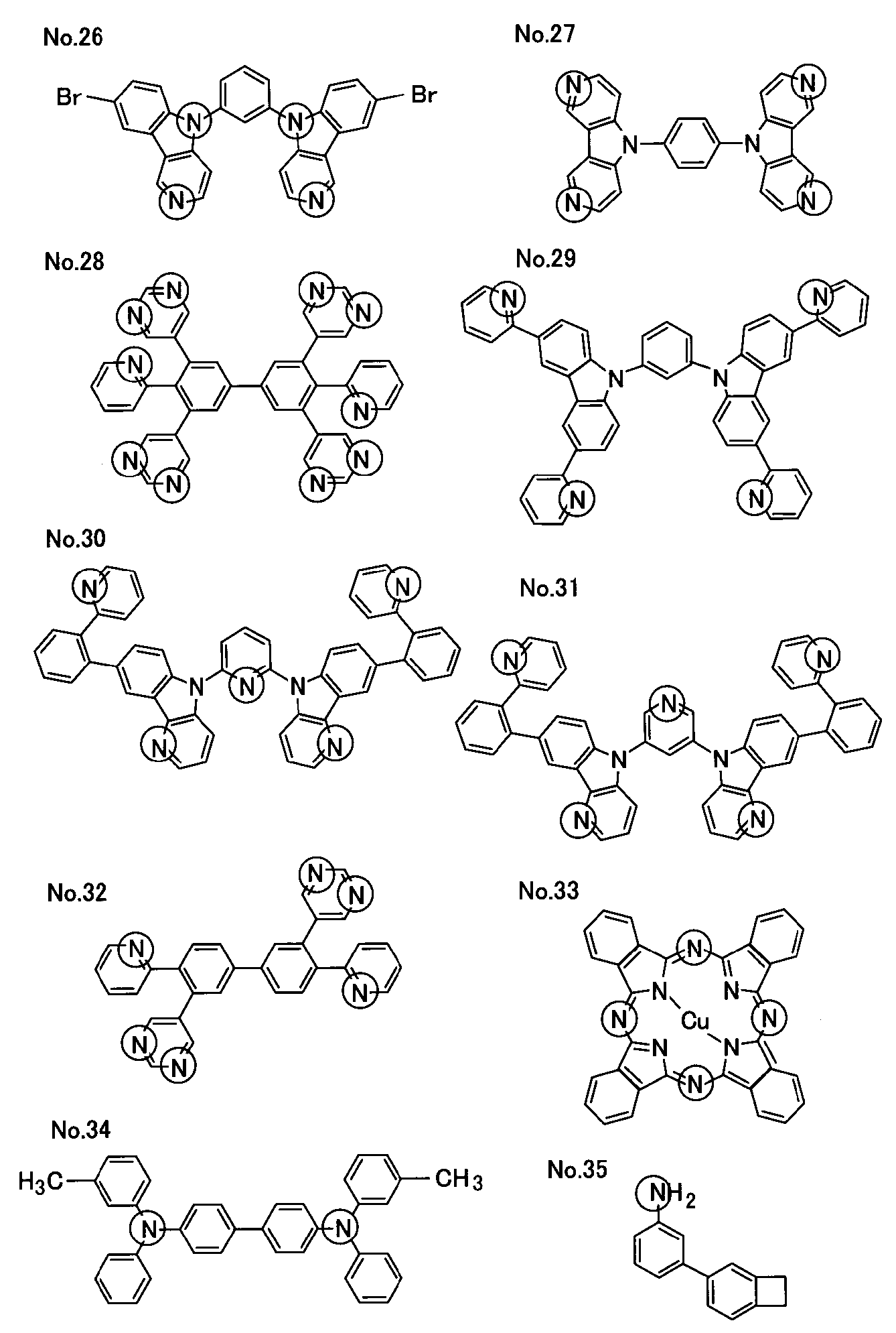

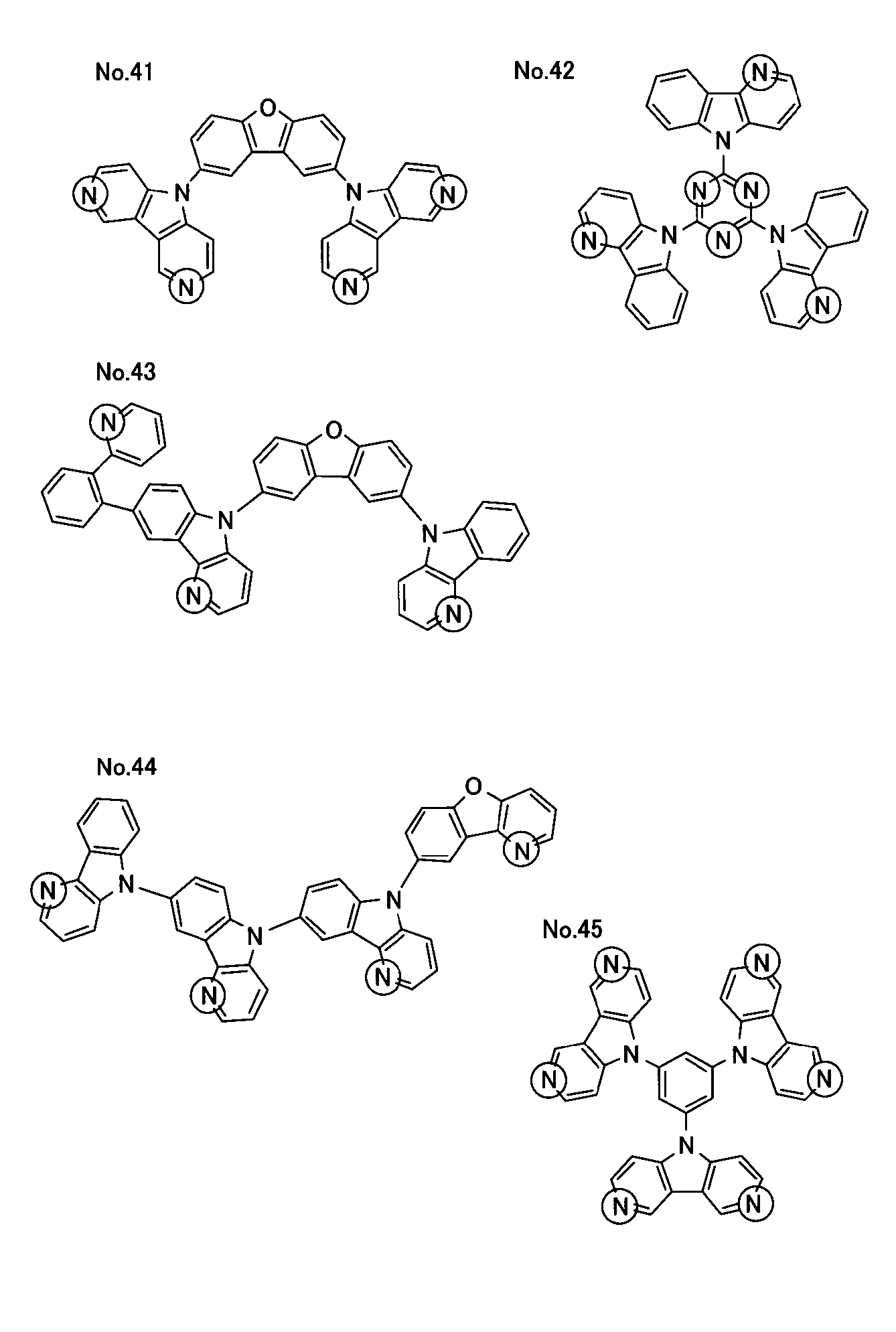
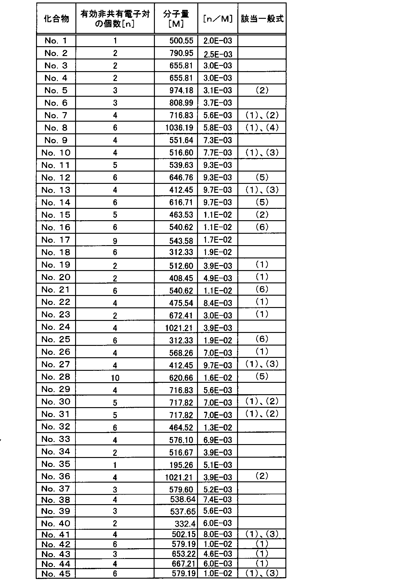
また窒素含有層1aを構成する化合物としては、以上のような有効非共有電子対含有率[n/M]が上述した所定範囲である化合物の他、この窒素含有層1aを備えた透明電極1が適用される電子デバイスごとに必要とされる性質を有する化合物が用いられる。例えば、この透明電極1が、有機電界発光素子の電極として用いられる場合、その成膜性や、電子輸送性の観点から、窒素含有層1aを構成する化合物としては、以降に説明する一般式(1)~(8a)で表される化合物が用いられる。


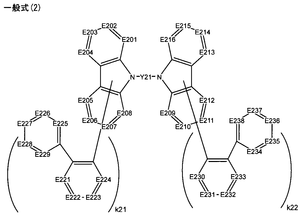
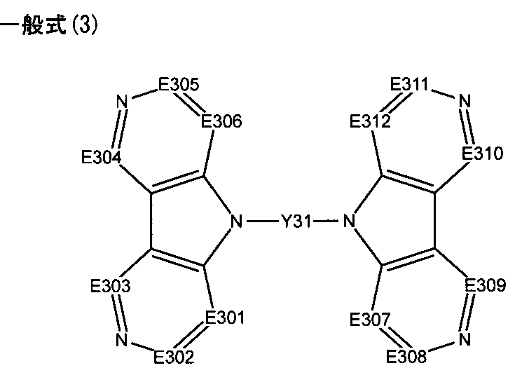


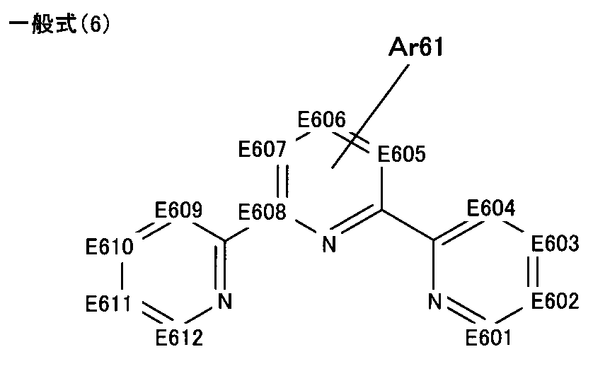


また窒素含有層1aを構成するさらに他の化合物として、以上のような一般式(1)~(8a)で表される化合物の他、下記に具体例を示す化合物1~166が例示される。これらの化合物は、電子輸送性または電子注入性を備えた材料である。したがって、これらの化合物を用いて窒素含有層1aを構成した透明電極1は、有機電界発光素子における透明電極として好適であり、有機電界発光素子における電子輸送層または電子注入層として窒素含有層1aを用いることができるのである。尚、これらの化合物1~166の中には、上述した有効非共有電子対含有率[n/M]の範囲に当てはまる化合物も含まれ、このような化合物であれば単独で窒素含有層1aを構成する化合物として用いることができる。さらに、これらの化合物1~166の中には、上述した一般式(1)~(8a)に当てはまる化合物もある。

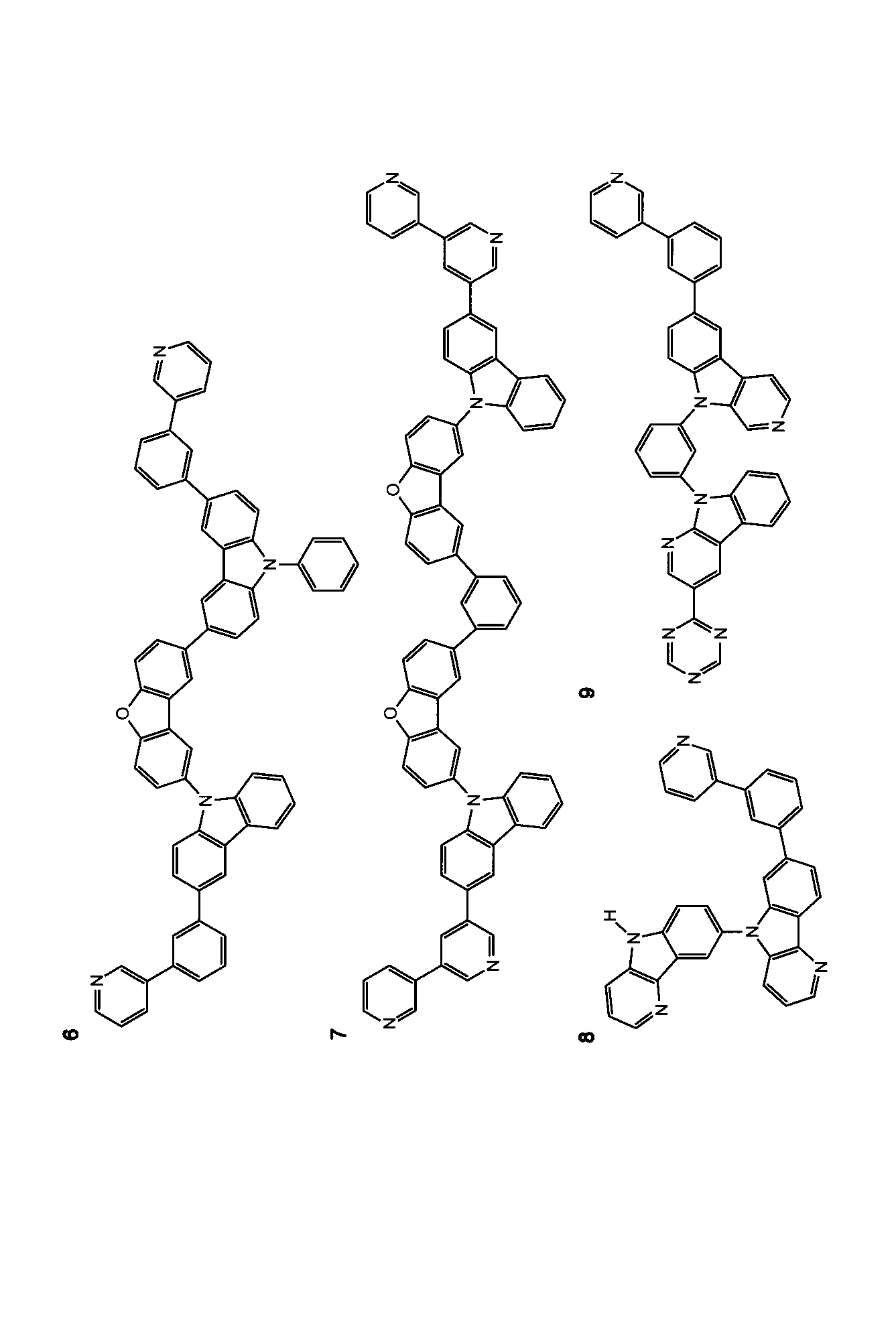


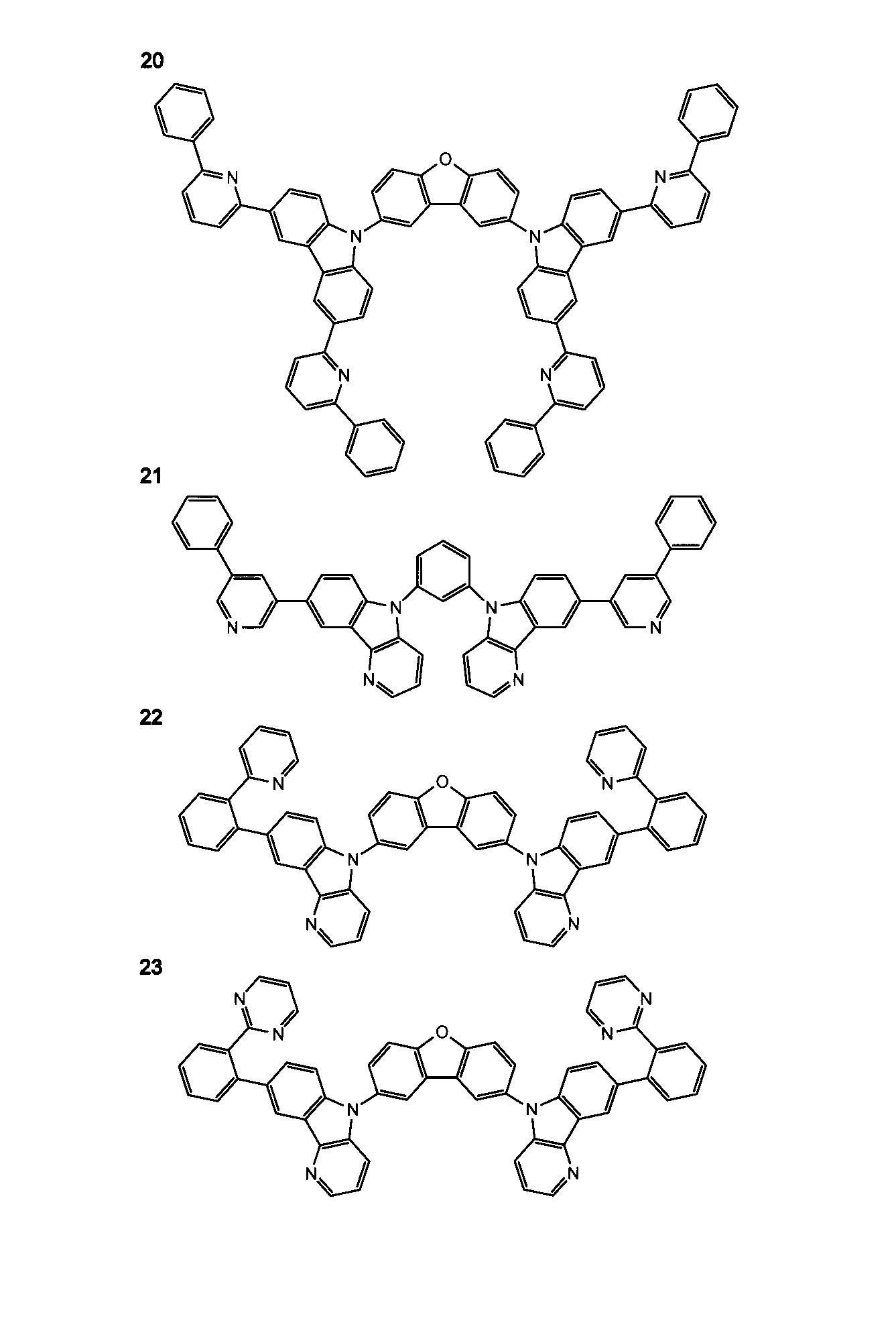


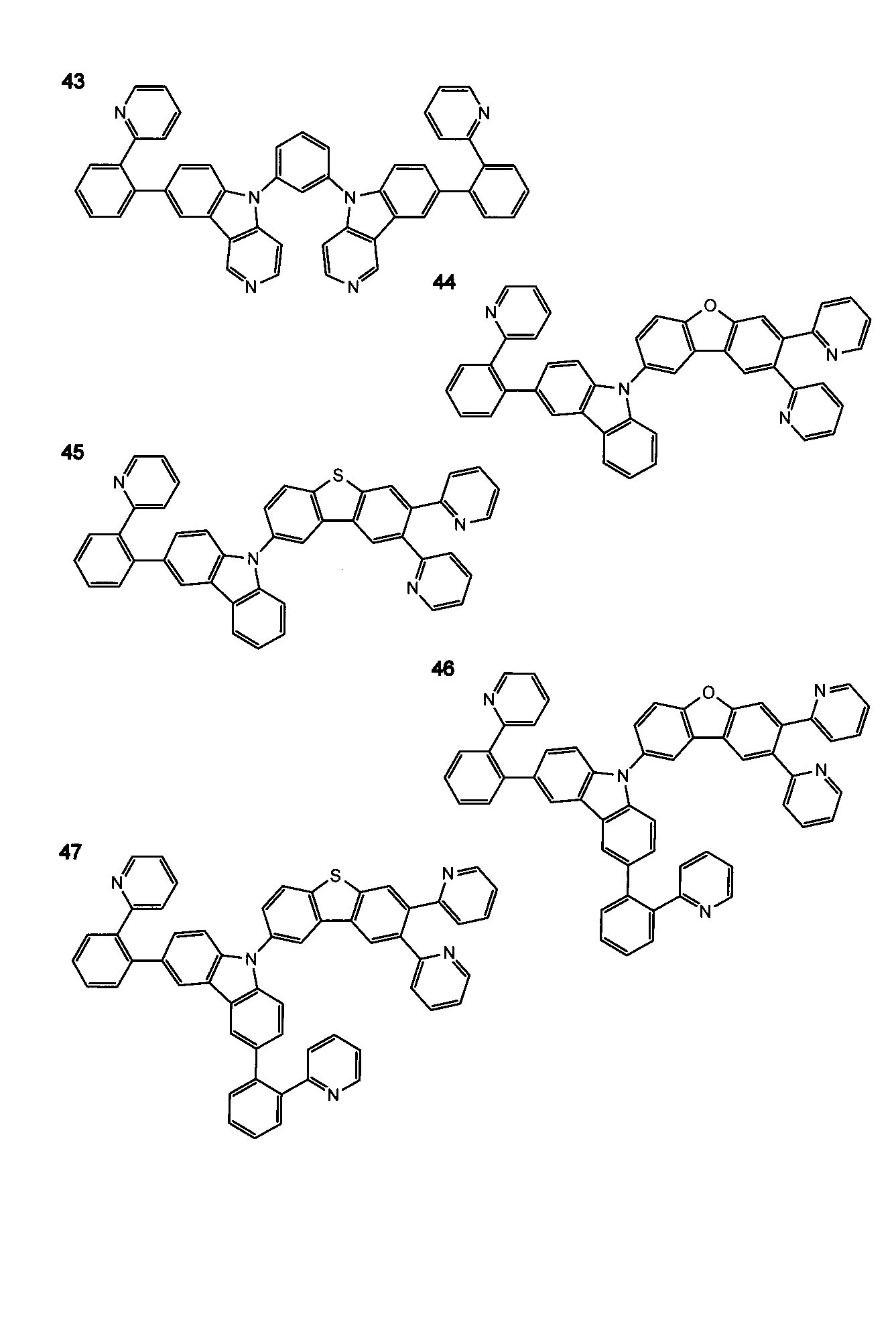
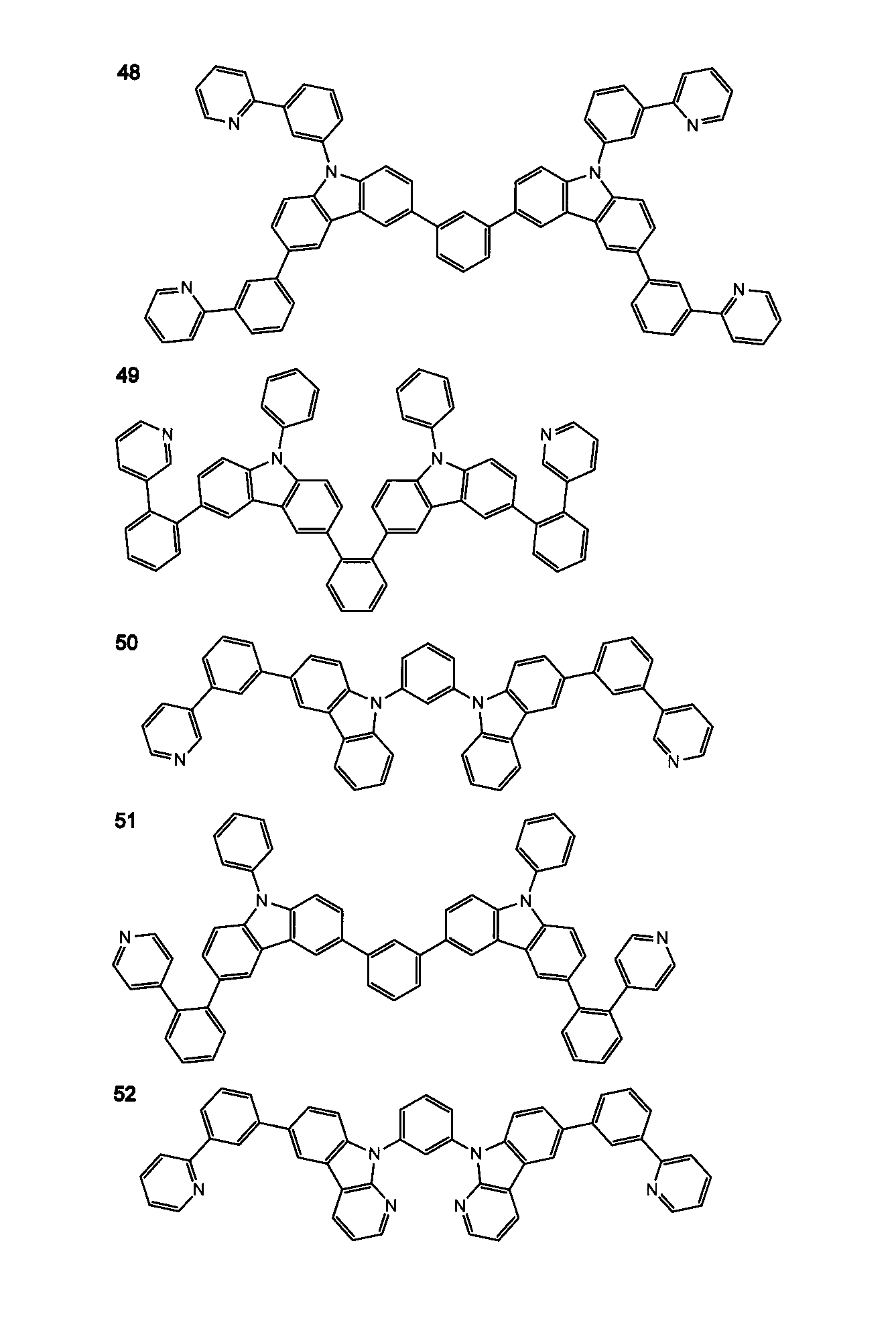


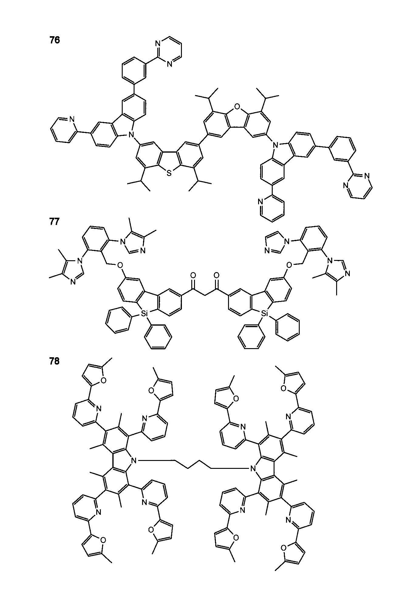


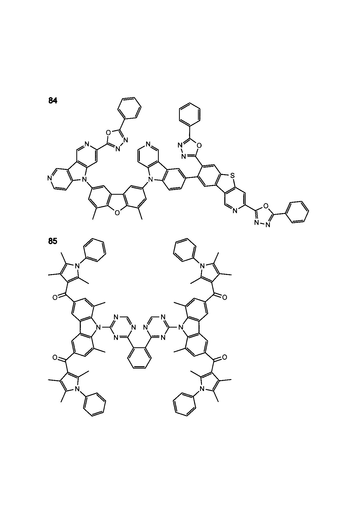


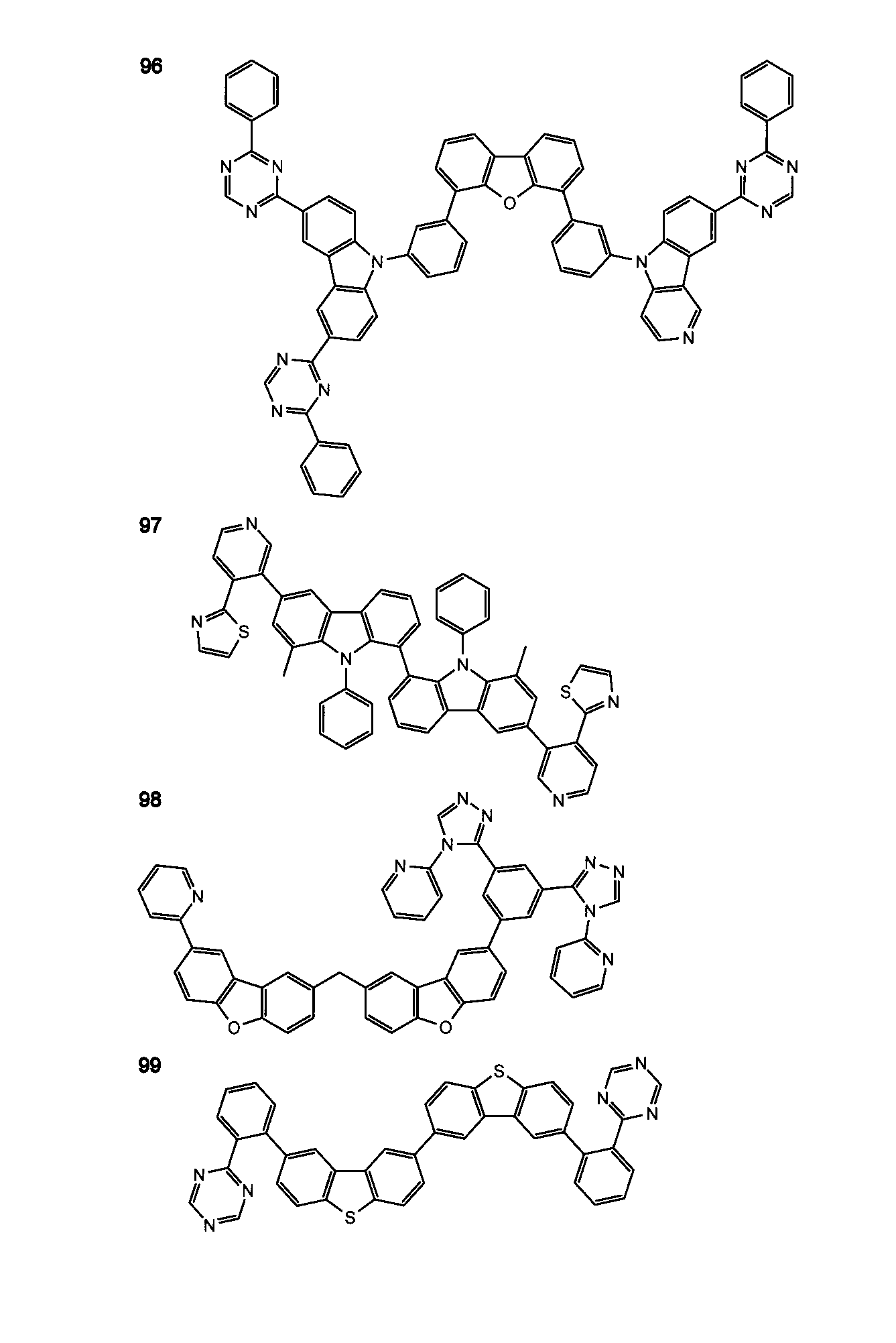

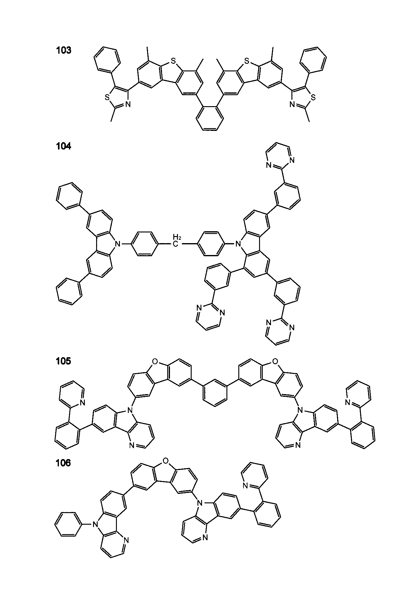
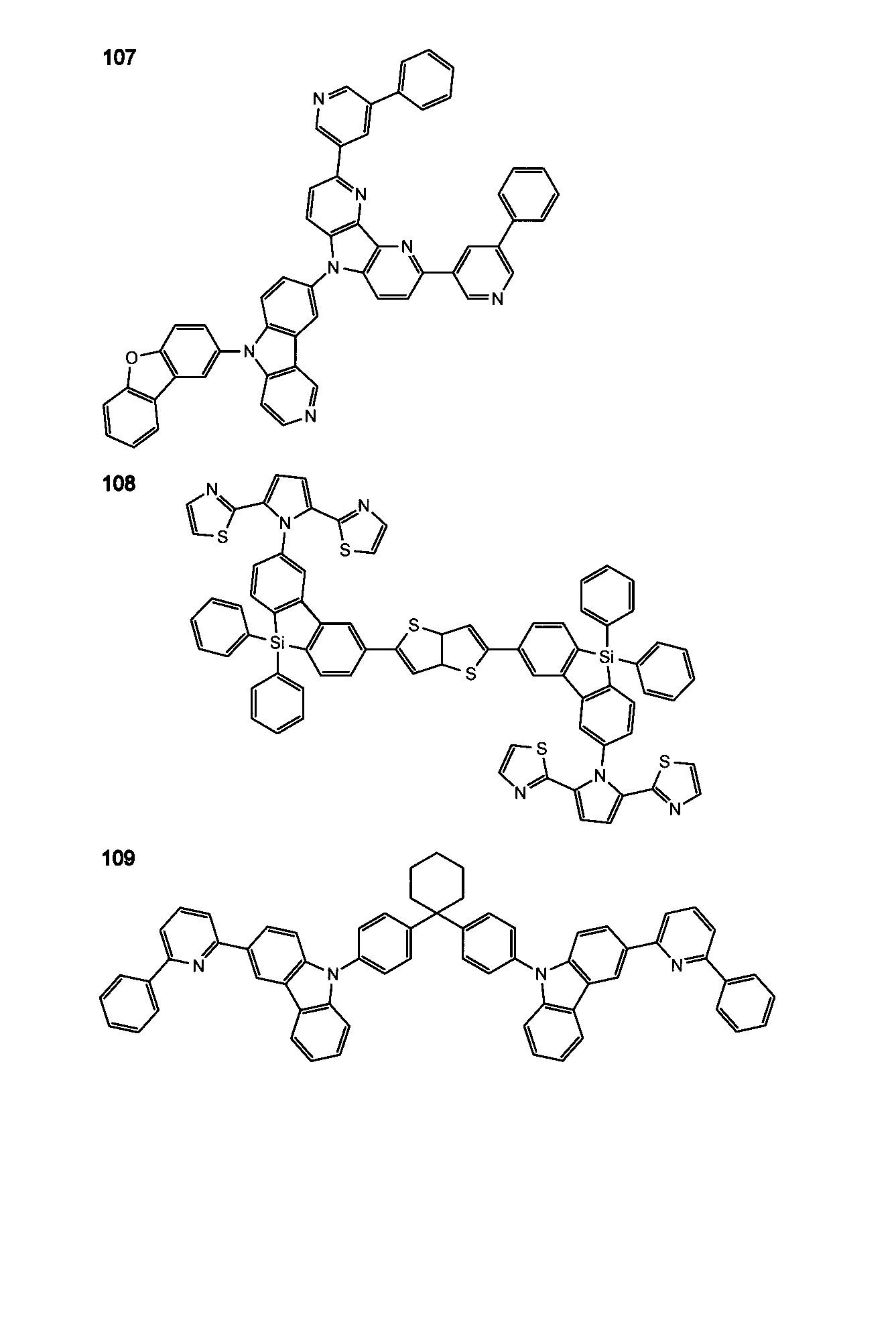


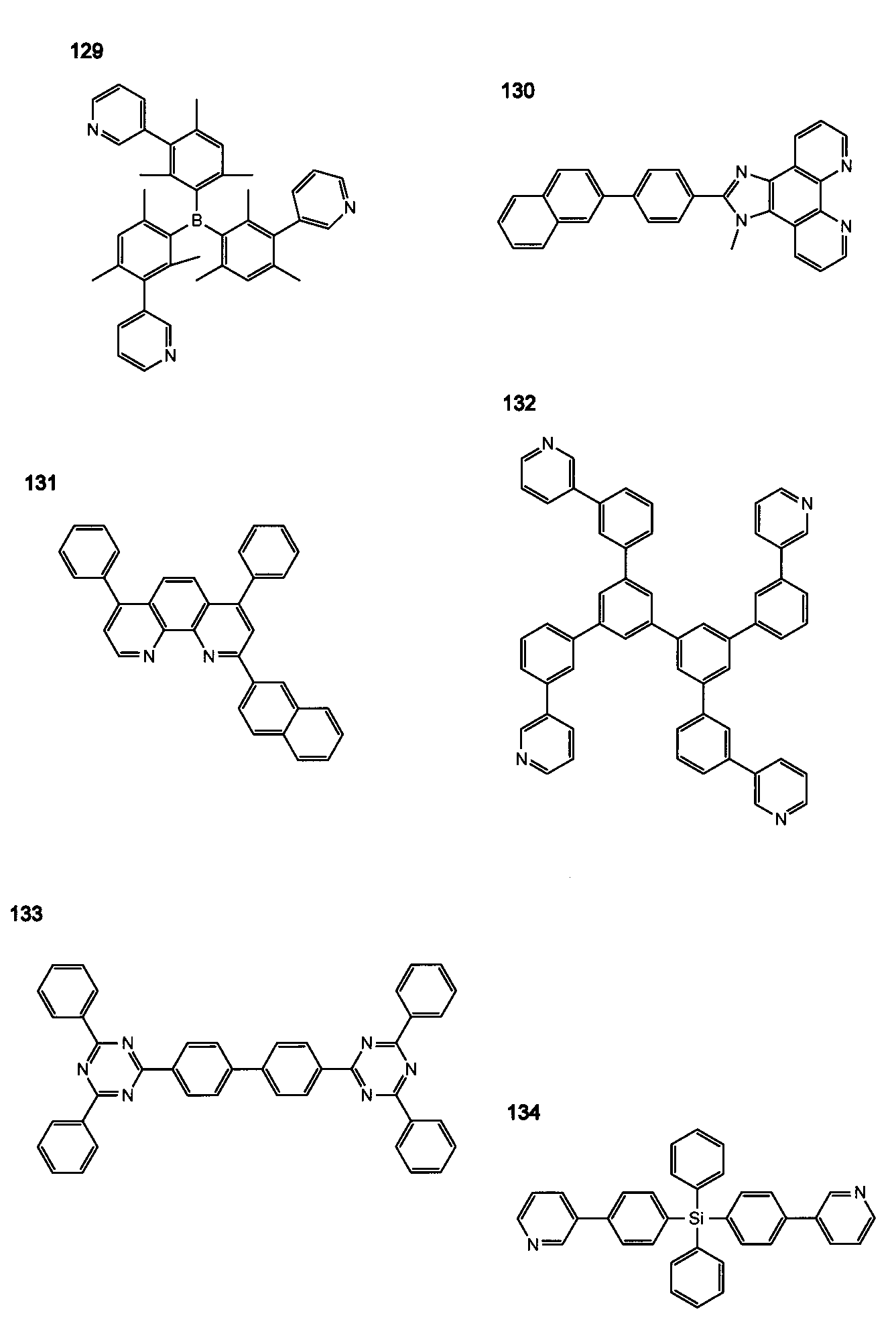


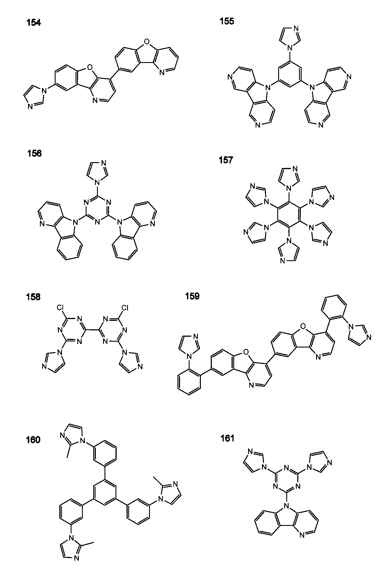

以下に代表的な化合物の合成例として、化合物5の具体的な合成例を示すが、これに限定されない。
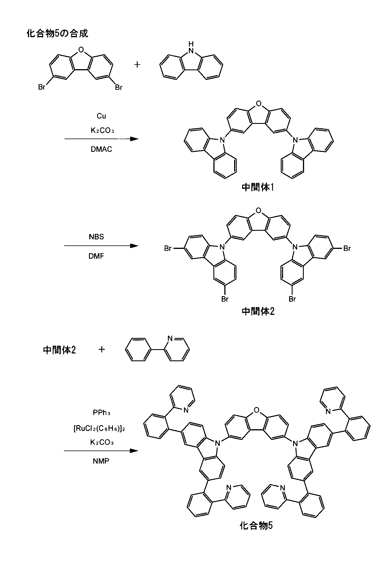
窒素雰囲気下、2,8-ジブロモジベンゾフラン(1.0モル)、カルバゾール(2.0モル)、銅粉末(3.0モル)、炭酸カリウム(1.5モル)を、DMAc(ジメチルアセトアミド)300ml中で混合し、130℃で24時間撹拌した。これによって得た反応液を室温まで冷却後、トルエン1Lを加え、蒸留水で3回洗浄し、減圧雰囲気下において洗浄物から溶媒を留去し、その残渣をシリカゲルフラッシュクロマトグラフィー(n-ヘプタン:トルエン=4:1~3:1)にて精製し、中間体1を収率85%で得た。
室温、大気下で中間体1(0.5モル)をDMF(ジメチルホルムアミド)100mlに溶解し、NBS(N-ブロモコハク酸イミド)(2.0モル)を加え、一晩室温で撹拌した。得られた沈殿を濾過し、メタノールで洗浄し、中間体2を収率92%で得た。
窒素雰囲気下、中間体2(0.25モル)、2-フェニルピリジン(1.0モル)、ルテニウム錯体[(η6-C6H6)RuCl2]2(0.05モル)、トリフェニルホスフィン(0.2モル)、炭酸カリウム(12モル)を、NMP(N-メチル-2-ピロリドン)3L中で混合し、140℃で一晩撹拌した。
以上のような窒素含有層1aが基材11上に成膜されたものである場合、その成膜方法としては、塗布法、インクジェット法、コーティング法、ディップ法などのウェットプロセスを用いる方法や、蒸着法(抵抗加熱法、電子ビーム蒸着法など)、スパッタ法、CVD法などのドライプロセスを用いる方法などが挙げられる。なかでも蒸着法が好ましく適用される。
高表面エネルギー材料層Aは、電極層1bを構成する銀(Ag)よりも、昇華熱エンタルピーが大きい高表面エネルギー材料を用いて構成された層であって、窒素含有層1aおよび電極層1bに接した状態で、これらの層間に設けられている。銀(Ag)よりも、昇華熱エンタルピーが大きい材料(高表面エネルギー材料)としては、アルミニウム(Al)、チタン(Ti)、金(Au)、プラチナ(Pt)等が例示される。高表面エネルギー材料層Aは、これらの材料のうちの少なくとも1つを用いて構成されると共に、これらの材料を主成分とし、その他の材料を含有していてもよい。その他の材料としては、銀(Ag)、マグネシウム(Mg)、銅(Cu)、インジウム(In)、リチウム(Li)などが用いられる。
電極層1bは、銀を主成分として構成された層であって、銀または銀を主成分とした合金を用いて構成され、窒素含有層1aとの間に高表面エネルギー材料層Aを挟持する状態で配置された層である。このような電極層1bは、高表面エネルギー材料層Aに隣接して設けられている。また、高表面エネルギー材料層Aが連続膜ではなく、島状であったり孔を有する層である場合、電極層1bの一部は窒素含有層1aに隣接して設けられている。
以上のように構成された透明電極1は、窒素原子を含有する化合物を用いて構成された窒素含有層1aと、銀(Ag)を主成分とした電極層1bとの間に、銀(Ag)よりも昇華熱エンタルピーが大きい材料を用いて構成された高表面エネルギー材料層Aを挟持した構成である。これにより、銀を主成分とする電極層1bは、高表面エネルギー材料層Aを構成する材料と銀(Ag)との相互作用、および窒素含有層1aを構成する窒素原子と銀(Ag)との相互作用により、隣接界面においての銀の拡散距離が減少して凝集が抑えられたものとなる。
上述した構成の透明電極1は、各種電子デバイスに用いることができる。電子デバイスの例としては、有機電界発光素子、LED(light Emitting Diode)、液晶素子、太陽電池、タッチパネル等が挙げられ、これらの電子デバイスにおいて光透過性を必要とされる電極部材として、上述の透明電極1を用いることができる。
<有機電界発光素子EL-1の構成>
図2は、本発明の電子デバイスの一例として、上述した透明電極1を用いた有機電界発光素子の第1例を示す断面構成図である。以下にこの図に基づいて有機電界発光素子の構成を説明する。
(1)陽極/発光層/陰極
(2)陽極/発光層/電子輸送層/陰極
(3)陽極/正孔輸送層/発光層/陰極
(4)陽極/正孔輸送層/発光層/電子輸送層/陰極
(5)陽極/正孔輸送層/発光層/電子輸送層/電子注入層/陰極
(6)陽極/正孔注入層/正孔輸送層/発光層/電子輸送層/陰極
(7)陽極/正孔注入層/正孔輸送層/(電子阻止層/)発光層/(正孔阻止層/)電子輸送層/電子注入層/陰極
上記の中で(7)の構成が好ましく用いられるが、これに限定されるものではない。
また、本発明に係る有機電界発光素子は、少なくとも1層の発光層を含む発光機能層を1つの発光ユニットとし、陽極と陰極との間にこの発光ユニット(発光機能層)を複数積層した、いわゆるタンデム構造の素子であってもよい。
[陽極/第1発光ユニット/中間層/第2発光ユニット/中間層/第3発光ユニット/陰極]
基板13は、先に説明した本発明の透明電極1が設けられる基材と同様のものが用いられる。ただしこの有機電界発光素子EL-1が、対向電極5-1側からも発光光hを取り出す両面発光型である場合、例示した基材のうちから光透過性を有する透明なものが選択して用いられる。
透明電極1は、先に説明した本発明の透明電極1であり、発光機能層3側から順に、窒素含有層1a、高表面エネルギー材料層A、および電極層1bを順に成膜した構成である。ここでは特に、透明電極1を構成する電極層1bおよび高表面エネルギー材料層Aが実質的な陰極となる。また本実施形態の有機電界発光素子EL-1においては、発光機能層3と、実質的な陰極として用いられる電極層1bとの間に、有機材料からなる窒素含有層1aが配置された構成となる。このため本実施形態における透明電極1の窒素含有層1aは、発光機能層3の一部を構成する層であるともみなされる。
対向電極5-1は、発光機能層3に正孔を供給するための陽極として機能する電極膜であり、発光機能層3に接する側の界面層が、陽極として適する材料で構成されていることとする。陽極として適する材料としては、仕事関数の大きい(4eV以上、好ましくは4.5eV以上)金属、合金、電気伝導性化合物及びこれらの混合物を電極物質とするものが好ましく用いられる。このような電極物質の具体例としては、Au等の金属、CuI、インジウムチンオキシド(ITO)、SnO2、ZnO等の導電性透明材料が挙げられる。また、IDIXO(In2O3-ZnO)等非晶質で透明導電膜を作製可能な材料を用いてもよい。
本発明に係る発光層は、電極または隣接層から注入されてくる電子及び正孔が再結合し、励起子を経由して発光する場を提供する層であり、発光する部分は発光層の層内であっても、発光層と隣接層との界面であってもよい。本発明に係る発光層は、本発明で規定する要件を満たしていれば、その構成に特に制限はない。
本発明に係る発光ドーパントについて説明する。
発光ドーパントとしては、蛍光発光性ドーパント(蛍光ドーパント、蛍光性化合物ともいう)と、リン光発光性ドーパント(リン光ドーパント、リン光性化合物ともいう)が好ましく用いられる。本発明においては、少なくとも1層の発光層がリン光発光ドーパントを含有することが好ましい。
本発明に係るリン光発光性ドーパント(以下、「リン光ドーパント」ともいう)について説明する。


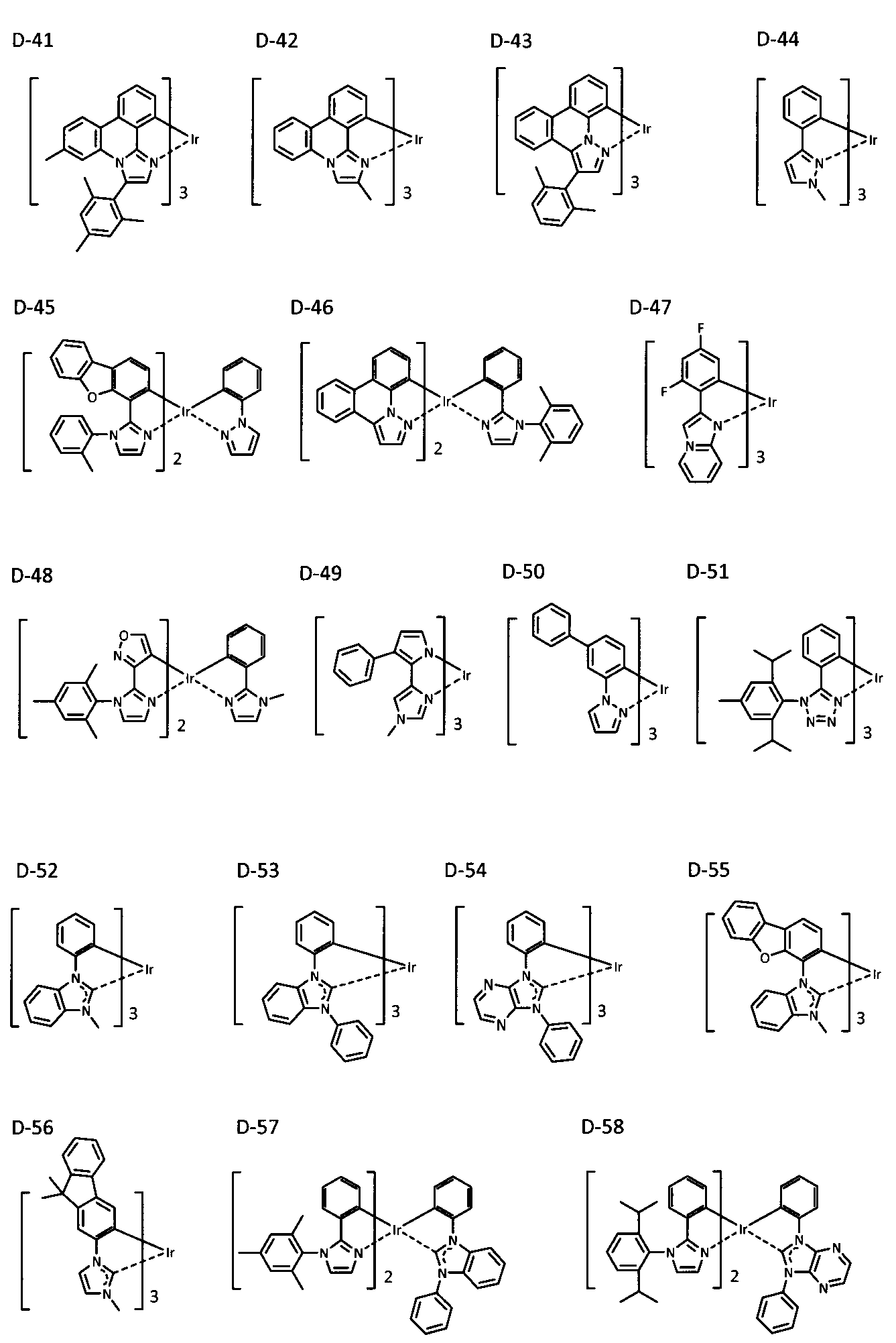
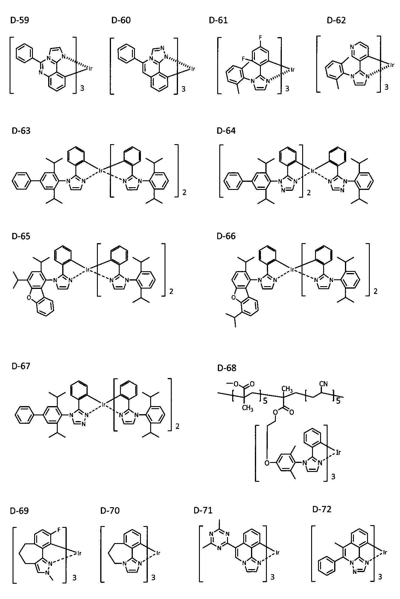
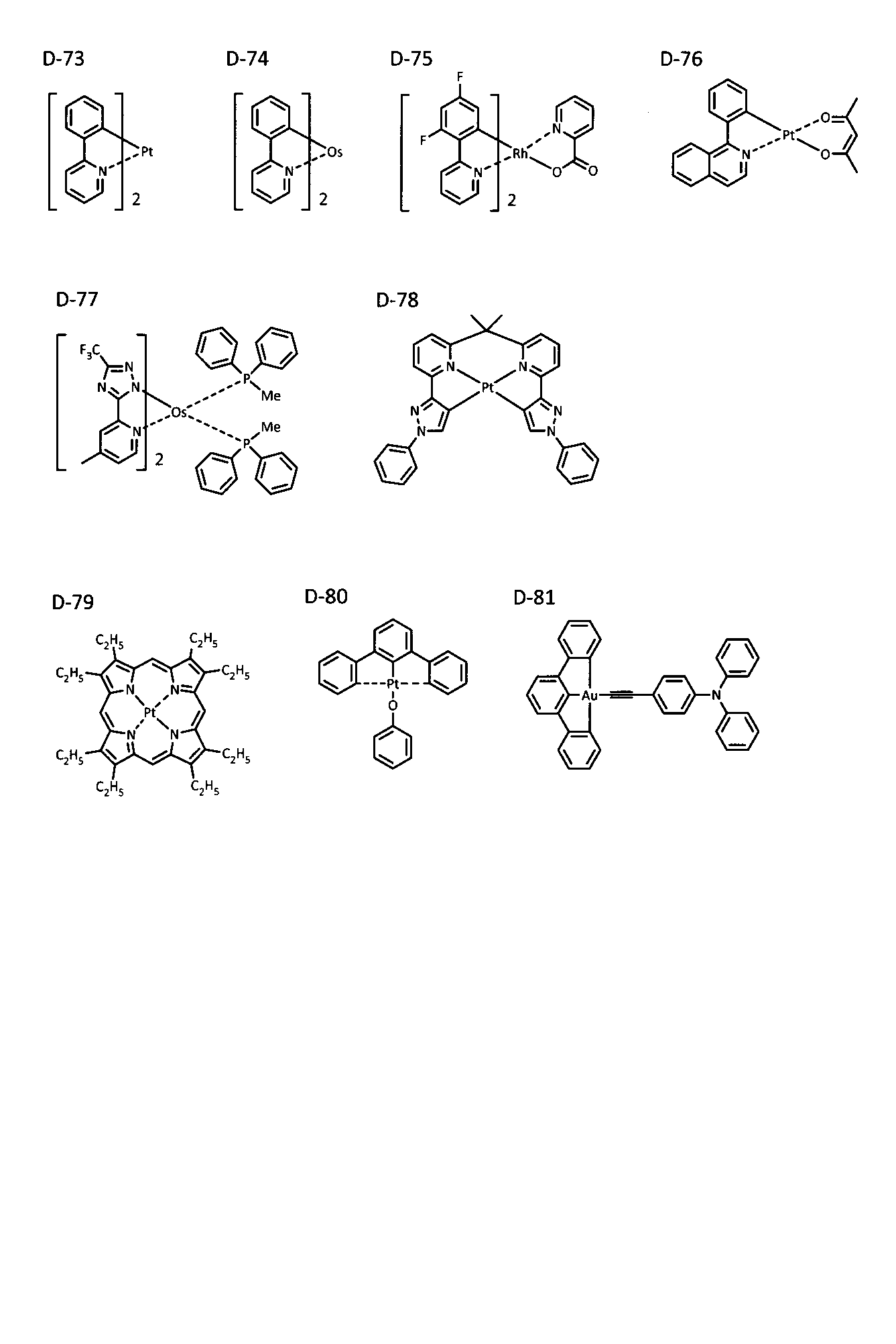
本発明に係る蛍光発光性ドーパント(以下、「蛍光ドーパント」ともいう)について説明する。
本発明に係るホスト化合物は、発光層において主に電荷の注入および輸送を担う化合物であり、有機EL素子においてそれ自体の発光は実質的に観測されない。
本発明において電子輸送層とは、電子を輸送する機能を有する材料からなり、陰極より注入された電子を発光層に伝達する機能を有していればよい。
また、これらの材料を高分子鎖に導入した、またはこれらの材料を高分子の主鎖とした高分子材料を用いることもできる。
正孔阻止層とは広い意味では電子輸送層の機能を有する層であり、好ましくは電子を輸送する機能を有しつつ正孔を輸送する能力が小さい材料からなり、電子を輸送しつつ正孔を阻止することで電子と正孔の再結合確率を向上させることができる。
本発明に係る電子注入層(「陰極バッファー層」ともいう)とは、駆動電圧低下や発光輝度向上のために陰極と発光層との間に設けられる層のことで、「有機EL素子とその工業化最前線(1998年11月30日エヌ・ティー・エス社発行)」の第2編第2章「電極材料」(123~166頁)に詳細に記載されている。
また、上記の電子注入層に用いられる材料は単独で用いてもよく、複数種を併用して用いてもよい。
本発明において正孔輸送層とは、正孔を輸送する機能を有する材料からなり、陽極より注入された正孔を発光層に伝達する機能を有していればよい。
電子阻止層とは広い意味では正孔輸送層の機能を有する層であり、好ましくは正孔を輸送する機能を有しつつ電子を輸送する能力が小さい材料からなり、正孔を輸送しつつ電子を阻止することで電子と正孔の再結合確率を向上させることができる。
[正孔注入層]
本発明に係る正孔注入層(「陽極バッファー層」ともいう)とは、駆動電圧低下や発光輝度向上のために陽極と発光層との間に設けられる層のことで、「有機EL素子とその工業化最前線(1998年11月30日エヌ・ティー・エス社発行)」の第2編第2章「電極材料」(123~166頁)に詳細に記載されている。
前述した発光機能層を構成する各層は、さらに他の含有物が含まれていてもよい。
含有物としては、例えば臭素、ヨウ素及び塩素等のハロゲン元素やハロゲン化化合物、Pd、Ca、Na等のアルカリ金属やアルカリ土類金属、遷移金属の化合物や錯体、塩等が挙げられる。
発光機能層を構成する各層(正孔注入層、正孔輸送層、発光層、正孔阻止層、電子輸送層、電子注入層等)の形成方法について説明する。
補助電極15は、透明電極1の抵抗を下げる目的で設けるものであって、透明電極1の電極層1bに接して設けられる。補助電極15を形成する材料は、金、白金、銀、銅、アルミニウム等の抵抗が低い金属が好ましい。これらの金属は光透過性が低いため、光取り出し面17aからの発光光hの取り出しの影響のない範囲でパターン形成される。このような補助電極15の形成方法としては、蒸着法、スパッタリング法、印刷法、インクジェット法、エアロゾルジェット法などが挙げられる。補助電極15の線幅は、光を取り出す開口率の観点から50μm以下であることが好ましく、補助電極15の厚さは、導電性の観点から1μ以上であることが好ましい。
透明封止材17は、有機電界発光素子EL-1を覆うものであって、板状(フィルム状)の封止部材であって接着剤19によって基板13側に固定されるものであっても良く、封止膜であっても良い。この透明封止材17の表面は、有機電界発光素子EL-1の発光光hを取り出す光取り出し面17aとなっている。このような透明封止材17は、有機電界発光素子EL-1における透明電極1および対向電極5-1の端子部分を露出させる状態で、少なくとも発光機能層3を覆う状態で設けられている。また透明封止材17に電極を設け、有機電界発光素子EL-1の透明電極1および対向電極5-1の端子部分と、この電極とを導通させるように構成されていても良い。
尚、ここでの図示は省略したが、基板13との間に有機電界発光素子ELおよび透明封止材17を挟んで保護膜もしくは保護板を設けても良い。この保護膜もしくは保護板は、有機電界発光素子ELを機械的に保護するためのものであり、特に透明封止材17が封止膜である場合には、有機電界発光素子ELに対する機械的な保護が十分ではないため、このような保護膜もしくは保護板を設けることが好ましい。
ここでは一例として、図2に示す有機電界発光素子EL-1の製造方法を説明する。
以上説明した有機電界発光素子EL-1は、本発明の導電性と光透過性とを兼ね備えた透明電極1を陰極として用い、この透明電極1における窒素含有層1a側に発光機能層3と陽極となる対向電極5-1とをこの順に設けた構成である。このため、透明電極1と対向電極5-1との間に十分な電圧を印加して有機電界発光素子EL-1での高輝度発光を実現しつつ、透明電極1側からの発光光hの取り出し効率が向上することによる高輝度化を図ることが可能である。さらに、所定輝度を得るための駆動電圧の低減による発光寿命の向上を図ることも可能になる。また有機電界発光素子EL-1は、均一な膜厚であることで平滑性の高い透明電極1を用いたことにより、整流比が向上し、短絡の可能性が低く信頼性の向上が図られたものとなる。
<有機電界発光素子の構成>
図3は、本発明の電子デバイスの一例として、上述した透明電極を用いた有機電界発光素子の第2例を示す断面構成図である。この図に示す第2例の有機電界発光素子EL-2が、図2を用いて説明した第1例の有機電界発光素子EL-1と異なるところは、透明基板13’上に透明電極1を設け、この上部に発光機能層3と対向電極5-2とをこの順に積層したところにある。以下、第1例と同様の構成要素についての重複する詳細な説明は省略し、第2例の有機電界発光素子EL-2の特徴的な構成を説明する。
以上説明した有機電界発光素子EL-2は、本発明の導電性と光透過性とを兼ね備えた透明電極1を陽極として用い、この上部に発光機能層3と陰極となる対向電極5-2とを設けた構成である。このため、第1例と同様に、透明電極1と対向電極5-2との間に十分な電圧を印加して有機電界発光素子EL-2での高輝度発光を実現しつつ、透明電極1側からの発光光hの取り出し効率が向上することによる高輝度化を図ることが可能である。さらに、所定輝度を得るための駆動電圧の低減による発光寿命の向上を図ることも可能になる。また有機電界発光素子EL-2は、均一な膜厚であることで平滑性の高い透明電極1を用いたことにより、第1例と同様に整流比が向上し、短絡の可能性が低く信頼性の向上が図られたものとなる。
<有機電界発光素子の構成>
図4は、本発明の電子デバイスの一例として、上述した透明電極を用いた有機電界発光素子の第3例を示す断面構成図である。この図に示す第3例の有機電界発光素子EL-3が、図2を用いて説明した第1例の有機電界発光素子EL-1と異なるところは、基板として透明基板13’を用い、2つの透明電極1間に発光機能層3を挟持させたところにある。以下、第1例と同様の構成要素についての重複する詳細な説明は省略し、第3例の有機電界発光素子EL-3の特徴的な構成を説明する。
以上説明した有機電界発光素子EL-3は、本発明の導電性と光透過性とを兼ね備えた透明電極1を陽極および陰極として用い、この間に発光機能層3を挟持した構成である。このため、第1例と同様に、2つの透明電極1間に十分な電圧を印加して有機電界発光素子EL-3での高輝度発光を実現しつつ、2つの透明電極1側からの発光光hの取り出し効率が向上することによる高輝度化を図ることが可能である。さらに、所定輝度を得るための駆動電圧の低減による発光寿命の向上を図ることも可能になる。また有機電界発光素子EL-3は、均一な膜厚であることで平滑性の高い透明電極1を用いたことにより、第1例と同様に整流比が向上し、短絡の可能性が低く信頼性の向上が図られたものとなる。
<有機電界発光素子の構成>
図5は、本発明の電子デバイスの一例として、上述した透明電極を用いた有機電界発光素子の第4例を示す断面構成図である。この図に示す第4例の有機電界発光素子EL-4が、図2を用いて説明した第1例の有機電界発光素子EL-1と異なるところは、透明基板13’側から順に陰極(透明電極1)、発光機能層3、陽極(対向電極5-4)を設けて積層順を逆にしたところにある。以下、第1例と同様の構成要素についての重複する詳細な説明は省略し、第4例の有機電界発光素子EL-4の特徴的な構成を説明する。
以上説明した有機電界発光素子EL-4は、本発明の導電性と光透過性とを兼ね備えた透明電極1を陰極として用い、この上部に発光機能層3と陽極となる対向電極5-4とをこの順に設けた構成である。このため、第1例と同様に、透明電極1と対向電極5-4との間に十分な電圧を印加して有機電界発光素子EL-4での高輝度発光を実現しつつ、透明電極1側からの発光光hの取り出し効率が向上することによる高輝度化を図ることが可能である。さらに、所定輝度を得るための駆動電圧の低減による発光寿命の向上を図ることも可能になる。また有機電界発光素子EL-4は、均一な膜厚であることで平滑性の高い透明電極1を用いたことにより、第1例と同様に整流比が向上し、短絡の可能性が低く信頼性の向上が図られたものとなる。
上述した各構成の有機電界発光素子は、上述したように面発光体であるため各種の発光光源として用いることができる。例えば、家庭用照明や車内照明などの照明装置、時計や液晶用のバックライト、看板広告用照明、信号機の光源、光記憶媒体の光源、電子写真複写機の光源、光通信処理機の光源、光センサーの光源等が挙げられるが、これに限定するものではなく、特にカラーフィルターと組み合わせた液晶表示装置のバックライト、照明用光源としての用途に有効に用いることができる。
本発明の照明装置は、上記有機電界発光素子を有する。
また本発明の有機電界発光素子は、複数用いて発光面を大面積化した照明装置としても用いることができる。この場合、透明基板上に有機電界発光素子を設けた複数の発光パネルを、支持基板上に複数配列する(すなわちタイリングする)ことによって発光面を大面積化する。支持基板は、封止材を兼ねるものであっても良く、この支持基板と、発光パネルの透明基板との間に有機電界発光素子を挟持する状態で各発光パネルをタイリングする。支持基板と透明基板との間には接着剤を充填し、これによって有機電界発光素子を封止しても良い。尚、発光パネルの周囲には、透明電極および対向電極の端子を露出させておく。
以降の表2に構成を示すように、試料101~132の各透明電極を、導電性領域の面積が5cm×5cmとなるように作製した。尚、ここでは、上記表1に示した化合物No.1~No.45の中から適宜選択した化合物を用いた。
以下のようにして、ガラス製の基材上に、下記表2に示すそれぞれの膜厚で銀(Ag)からなる電極層を形成した。
以下のようにして、ガラス製の基材上に、下記表2に示すそれぞれの材料を用いた窒素含有層と、銀からなる電極層との2層構造の透明電極を形成した。尚、試料103では、窒素含有層に換えて窒素を含有しない下地層を形成した。
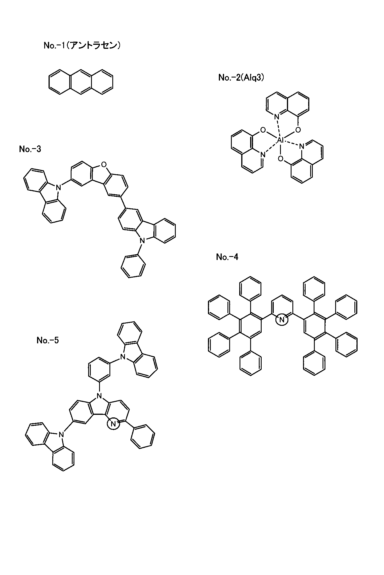
以下のようにして、ガラス製の基材上に、下記表2に示すそれぞれの材料を用いた窒素含有層と、プラチナ(Pt)からなる高表面エネルギー材料層と、銀からなる電極層との3層構造の透明電極を形成した。
上記試料112~114と同様の手順で、試料115~127の各透明電極を得た。ただし、窒素含有層を構成する化合物は下記表2に示す通りであり、高表面エネルギー材料層を構成する材料としてチタン(Ti)を用いた。チタン(Ti)からなる高表面エネルギー層の形成は、窒素含有層および電極層の形成とは別の真空槽内において電子ビーム蒸着法によって行った。
上記試料112~114と同様の手順で、試料128,129の各透明電極を得た。ただし、窒素含有層を構成する化合物として下記表2に示す各材料を用い、高表面エネルギー材料層を構成する材料としてチタン(Ti)を用い、銀からなる電極層の膜厚を8nmとした。チタン(Ti)からなる高表面エネルギー層の形成は、窒素含有層および電極層の形成とは別の真空槽内において電子ビーム蒸着法によって行った。
上記試料112~114と同様の手順で、試料128,129の各透明電極を得た。ただし、基材としてポリエチレンテレフタレート(PET)を用い、窒素含有層を構成する化合物として下記表2に示す各材料を用い、高表面エネルギー材料層を構成する材料としてチタン(Ti)を用い、銀からなる電極層の膜厚を8nmとした。チタン(Ti)からなる高表面エネルギー層の形成は、窒素含有層および電極層の形成とは別の真空槽内において電子ビーム蒸着法によって行った。
上記試料115のようにして作製した透明電極の電極層上に、さらに酸化チタン(TiO2)からなる高屈折率層を膜厚50nmで形成した。高屈折率層の形成は、電極層の形成に引き続き、電極層の形成とは別の真空槽内において電子ビーム蒸着法によって行った。
上記で作製した試料101~132の各透明電極について、波長550nmの光に対する光透過率、およびシート抵抗値を測定した。光透過率の測定は、分光光度計(日立製作所製U-3300)を用い、試料と同じ基材をベースラインとして行った。シート抵抗値の測定は、抵抗率計(三菱化学社製MCP-T610)を用い、4端子4探針法定電流印加方式で行った。この結果を下記表2に合わせて示す。
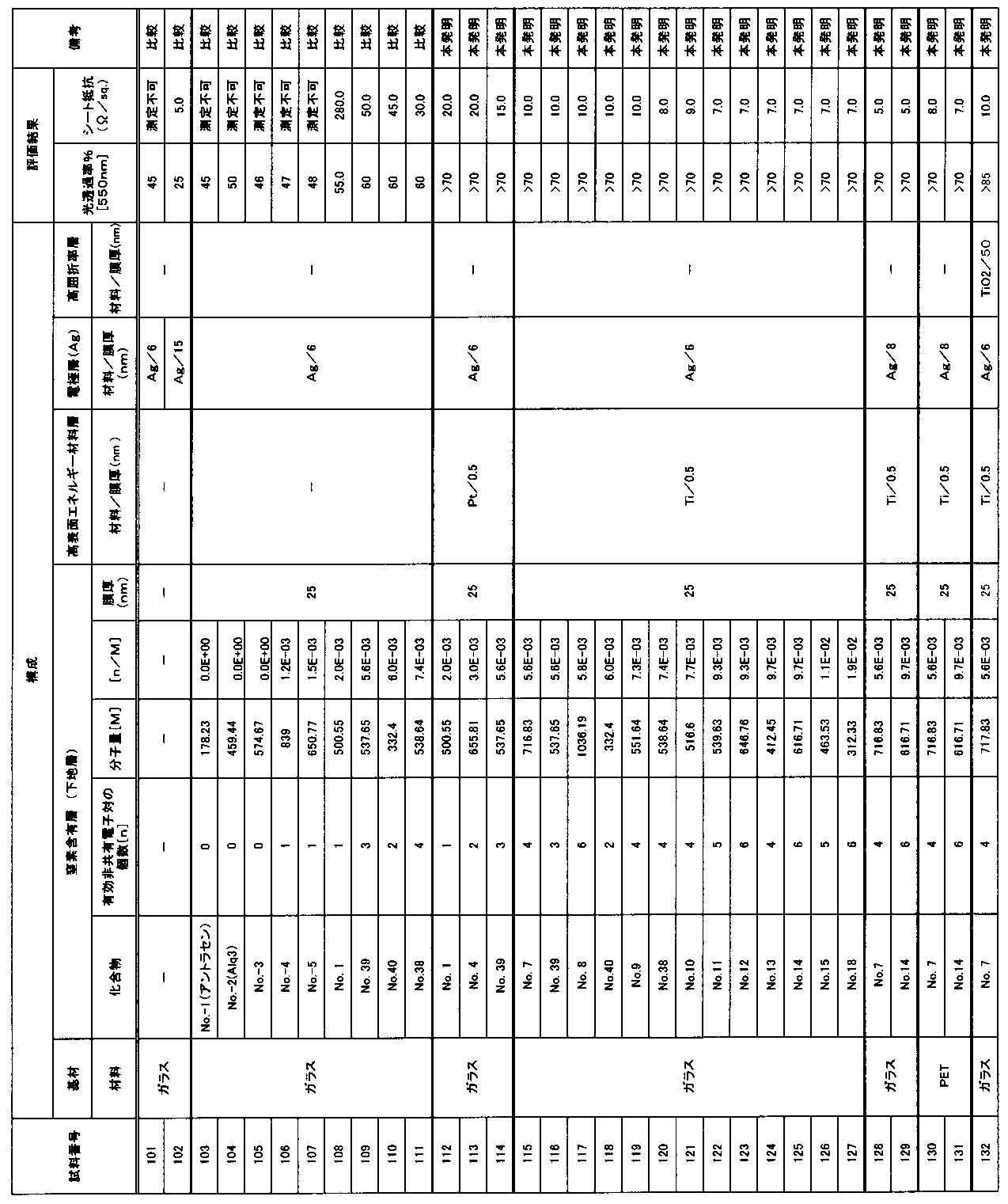
表2から明らかなように、試料112~132の透明電極、すなわち有効非共有電子対含有率[n/M]が2.0×10-3≦[n/M]の確認された所定範囲内である化合物No.1~No.45を用いて構成された窒素含有層と、この上部の高表面エネルギー材料層と、銀で構成された電極層とを備えた透明電極は、実質的な導電性を担う電極層が8nmまたは6nmと極薄膜でありながらも、シート抵抗値の値が20Ω/sq.以下の低い値に抑えられていた。このことから、本発明構成の透明電極では、高表面エネルギー材料層を介して窒素含有層上に形成された電極層が、単層成長型(Frank-van der Merwe:FM型)の膜成長によってほぼ均一な膜厚で形成されていることが確認された。
以降の表3に構成を示すように、各構成の透明電極を陽極として発光機能層の下部に設けた試料201~216のボトムエミッション型の各有機電界発光素子を作製した。図7を参照し、作製手順を説明する。尚、下記表3には、試料201~216の有機電界発光素子に用いた透明電極の構成を示した。各透明電極を構成する各層の形成手順は実施例1で説明した手順と同様である。またここで用いた各化合物は、実施例1で用いた化合物の中からさらに選択した化合物である。
(透明電極1の形成)
先ず試料201~216において、透明なPET製の透明基板13’の上部に、下記表3に示した各化合物で構成された窒素含有層1aを25nmの膜厚で形成した。
先ず、正孔輸送注入材料として下記構造式に示すα-NPDが入った加熱ボートに通電して加熱し、α-NPDよりなる正孔注入層と正孔輸送層とを兼ねた正孔輸送・注入層31を、透明電極1上に成膜した。この際、蒸着速度0.1nm/秒~0.2nm/秒、膜厚20nmとした。

次に、下記構造式に示すホスト材料H-1の入った加熱ボートと、下記構造式に示す燐光発光性化合物Ir1の入った加熱ボートとを、それぞれ独立に通電し、ホスト材料H-1と燐光発光性化合物Ir1とよりなる発光層32を、正孔輸送・注入層31上に成膜した。この際、蒸着速度がホスト材料H-1:燐光発光性化合物Ir1=100:6となるように、加熱ボートの通電を調節した。また膜厚30nmとした。

次いで、正孔阻止材料として下記構造式に示すBAlqが入った加熱ボートに通電して加熱し、BAlqよりなる正孔阻止層33を、発光層32上に成膜した。この際、蒸着速度0.1nm/秒~0.2nm/秒、膜厚10nmとした。

その後、電子輸送材料として、先に構造式を示した化合物10の入った加熱ボートと、フッ化カリウムの入った加熱ボートとをそれぞれ独立に通電し、化合物10とフッ化カリウムとよりなる電子注入層と電子輸送層とを兼ねた電子輸送・注入層34を、正孔阻止層33上に成膜した。この際、蒸着速度が化合物10:フッ化カリウム=75:25になるように、加熱ボートの通電を調節した。また膜厚30nmとした。尚、化合物10は、有効非共有電子対含有率[n/M]が所定範囲である化合物No.7でもある。
以上の後には、発光機能層3が形成された透明基板13’を、真空蒸着装置の第2真空槽内に移送し、第2真空槽内を4×10⁻⁴Paまで減圧した後、第2真空槽内に取り付けられたアルミニウムの入った加熱ボートを通電して加熱した。これにより、蒸着速度0.3nm/秒で膜厚100nmのアルミニウムからなる対向電極5-2を形成した。この対向電極5-2は、陰極として用いられる。以上により透明基板13’上に、ボトムエミッション型の有機電界発光素子EL-2を形成した。
その後、有機電界発光素子EL-2を、厚さ300μmのガラス基板からなる封止材17’で覆い、有機電界発光素子EL-2を囲む状態で、封止材17’と透明基板13’との間に接着剤19(シール材)を充填した。接着剤19としては、エポキシ系光硬化型接着剤(東亞合成社製ラックストラックLC0629B)を用いた。封止材17’と透明基板13’との間に充填した接着剤19に対して、ガラス基板からなる封止材17’側からUV光を照射し、接着剤19を硬化させて有機電界発光素子EL-2を封止した。
試料201~216で作製した有機電界発光素子EL-2(発光パネル)について、駆動電圧の測定、輝度ムラおよび高温・高湿保存性の評価を行った。この結果を下記表3に合わせて示す。

表3から明らかなように、試料204~216の有機電界発光素子、すなわち有効非共有電子対含有率[n/M]が2.0×10-3≦[n/M]である化合物No.1~No.45のうちの何れかを用いた窒素含有層1aと、この上部の高表面エネルギー材料層Aと、銀で構成された電極層1bとを備えた透明電極1を有する有機電界発光素子EL-2は、駆動電圧が10V以下、具体的には6V以下の低い駆動電圧で1000cd/m2の正面輝度の発光が得られることが確認された。またこれらの試料204~216の有機電界発光素子EL-2は、発光面内の均一性を示す輝度ムラの値が90%を越えて大きく輝度ムラの発生が小さく抑えられていることが確認された。さらにこれらの試料204~216の有機電界発光素子EL-2は、高温・高湿環境下での保存後にも発光が確認され、駆動電圧差ΔVも低い値であり、保存後の整流比も十分でリークが抑えられており、高温・高湿保存性にも優れていることが確認された。またこれにより、銀からなる電極層1bが連続膜として構成されてバリア性を発揮し、有機材料で構成された発光機能層3の劣化が防止されていることが確認された。


Claims (17)
- 窒素原子を含有すると共に当該窒素原子が有する非共有電子対のうち芳香族性に関与せずかつ金属に配位していない非共有電子対の数をn、分子量をMとした場合の有効非共有電子対含有率[n/M]が2.0×10-3≦[n/M]となる化合物を用いて構成された窒素含有層と、
銀を主成分とする電極層と、
銀よりも昇華熱エンタルピーが大きい高表面エネルギー材料を用いて構成され、前記窒素含有層と前記電極層とに接してこれらの間に挟持された高表面エネルギー材料層とを備えた
透明電極。 - 前記化合物における前記有効非共有電子対含有率[n/M]が、3.9×10-3≦[n/M]である
請求項1記載の透明電極。 - 前記化合物における前記有効非共有電子対含有率[n/M]が、6.5×10-3≦[n/M]である
請求項1に記載の透明電極。 - 前記窒素含有層は、前記化合物と共に他の化合物を用いて構成され、これらの化合物の混合比を考慮した前記有効非共有電子対含有率[n/M]の平均値が、2.0×10-3≦[n/M]である
請求項1~3に記載の透明電極。 - 前記窒素含有層は、下記一般式(1)で表される化合物を含有する
請求項1~4の何れかに記載の透明電極。
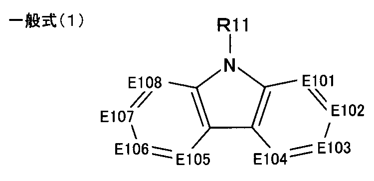
またR11および上記R12は水素原子または置換基を表す。] - 前記窒素含有層は、
前記一般式(1)におけるE103およびE106を-N=とした下記一般式(1a)で表される化合物を含有する
請求項5記載の透明電極。

- 前記窒素含有層は、下記一般式(2)で表される化合物を含有する
請求項1~4の何れかに記載の透明電極。

E201~E216、E221~E238は、各々-C(R21)=または-N=を表し、上記R21は水素原子または置換基を表す。
またE221~E229の少なくとも1つおよびE230~E238の少なくとも1つは-N=を表す。
k21およびk22は0~4の整数を表すが、k21+k22は2以上の整数である。〕 - 前記窒素含有層は、下記一般式(3)で表される化合物を含有する
請求項1~4の何れかに記載の透明電極。
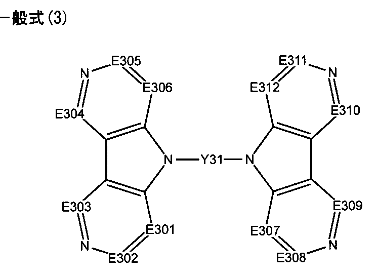
Y31は、アリーレン基、ヘテロアリーレン基またはそれらの組み合わせからなる2価の連結基を表す。] - 前記窒素含有層は、下記一般式(4)で表される化合物を含有する
請求項1~4の何れかに記載の透明電極。
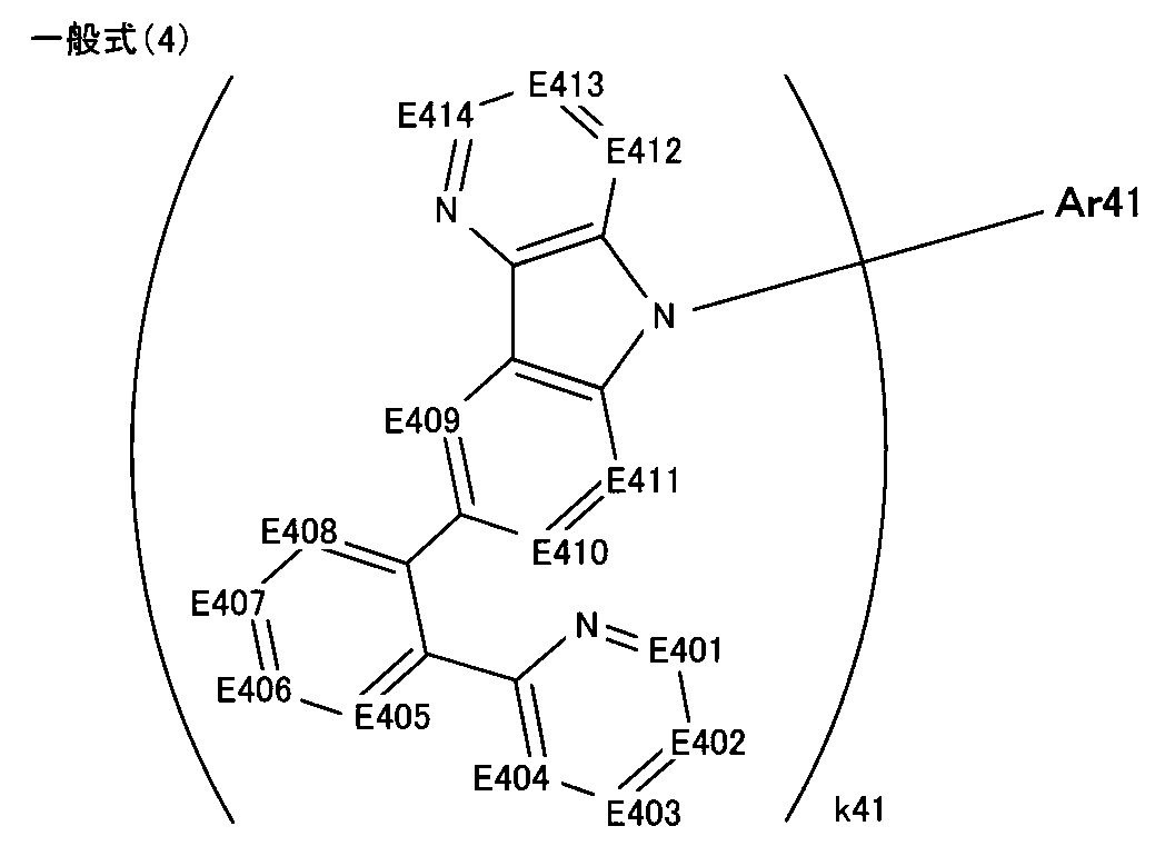
Ar41は、置換あるいは無置換の、芳香族炭化水素環あるいは芳香族複素環を表す。
またk41は3以上の整数を表す。] - 前記窒素含有層は、下記一般式(5)で表される化合物を含有する
請求項1~4の何れかに記載の透明電極。

R51は置換基を表し、
E501,E502、E511~E515、E521~E525は、各々-C(R52)=または-N=を表し、
E503~E505は、各々-C(R52)=を表し、
前記R52は、水素原子(H)または置換基を表し、
E501およびE502のうち少なくとも1つは-N=であり、
E511~E515のうち少なくとも1つは-N=であり、
E521~E525のうち少なくとも1つは-N=である。〕 - 前記窒素含有層は、下記一般式(6)で表される化合物を含有する
請求項1~4の何れかに記載の透明電極。

Ar61は、置換あるいは無置換の、芳香族炭化水素環あるいは芳香族複素環を表す。] - 前記窒素含有層は、下記一般式(7)で表される化合物を含有する
請求項1~4のいずれかに記載の透明電極。

R71~R73は、各々水素原子(H)または置換基を表し、
Ar71は、芳香族炭化水素環基または芳香族複素環基を表す。〕 - 前記窒素含有層は、下記一般式(8)で表される化合物を含有する
請求項1~4のいずれかに記載の透明電極。

R81~R86は、各々水素原子(H)または置換基を表し、
E801~E803は、各々-C(R87)=または-N=を表し、
前記R87は、水素原子(H)または置換基を表し、
Ar81は、芳香族炭化水素環基または芳香族複素環基を表す。〕 - 前記窒素含有層は、下記一般式(8a)で表される化合物を含有する
請求項13に記載の透明電極。
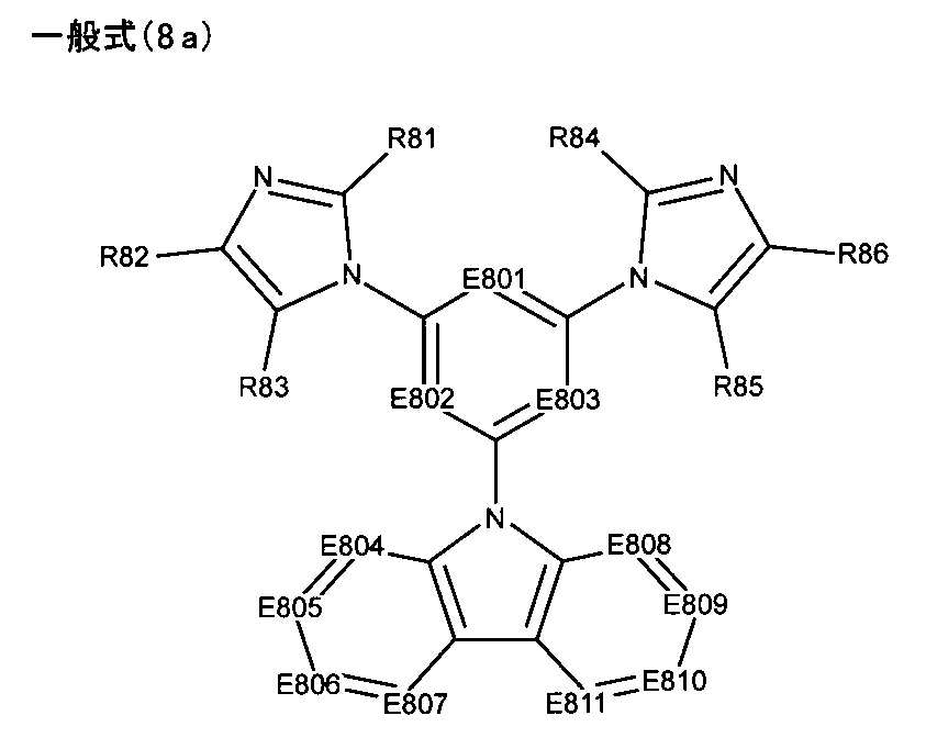
E804~E811は、各々-C(R88)=または-N=を表し、
前記R88は、それぞれが水素原子(H)または置換基と表し、
E808~E811のうち少なくとも一つは-N=であり、
E804~E807、E808~E811は、各々互いに結合して新たな環を形成してもよい。〕 - 前記高表面エネルギー材料として、アルミニウム(Al)、金(Au)、およびチタン(Ti)の少なくとも1つが用いられる
請求項1~14の何れかに記載の透明電極。 - 請求項1~15の何れかに記載の透明電極を有する
電子デバイス。 - 窒素原子を含有すると共に当該窒素原子が有する非共有電子対のうち芳香族性に関与せずかつ金属に配位していない非共有電子対の数をn、分子量をMとした場合の有効非共有電子対含有率[n/M]が2.0×10-3≦[n/M]となる化合物を用いて窒素含有層を形成する工程と、
前記窒素含有層に接して、銀よりも昇華熱エンタルピーが大きい高表面エネルギー材料を用いて高表面エネルギー材料層を形成する工程と、
前記高表面エネルギー材料層が設けられた前記窒素含有層上に銀を主成分とする電極層を形成する工程とを有する
透明電極の製造方法。
Priority Applications (3)
| Application Number | Priority Date | Filing Date | Title |
|---|---|---|---|
| US14/415,066 US20150207080A1 (en) | 2012-08-24 | 2013-08-21 | Transparent electrode, electronic device, and method for manufacturing transparent electrode |
| JP2014531648A JP6217642B2 (ja) | 2012-08-24 | 2013-08-21 | 透明電極、電子デバイス、および透明電極の製造方法 |
| EP13830585.9A EP2890221A4 (en) | 2012-08-24 | 2013-08-21 | TRANSPARENT ELECTRODE, ELECTRONIC DEVICE AND METHOD FOR PRODUCING THE TRANSPARENT ELECTRODE |
Applications Claiming Priority (2)
| Application Number | Priority Date | Filing Date | Title |
|---|---|---|---|
| JP2012-185433 | 2012-08-24 | ||
| JP2012185433 | 2012-08-24 |
Publications (1)
| Publication Number | Publication Date |
|---|---|
| WO2014030666A1 true WO2014030666A1 (ja) | 2014-02-27 |
Family
ID=50149972
Family Applications (1)
| Application Number | Title | Priority Date | Filing Date |
|---|---|---|---|
| PCT/JP2013/072269 WO2014030666A1 (ja) | 2012-08-24 | 2013-08-21 | 透明電極、電子デバイス、および透明電極の製造方法 |
Country Status (4)
| Country | Link |
|---|---|
| US (1) | US20150207080A1 (ja) |
| EP (1) | EP2890221A4 (ja) |
| JP (1) | JP6217642B2 (ja) |
| WO (1) | WO2014030666A1 (ja) |
Cited By (3)
| Publication number | Priority date | Publication date | Assignee | Title |
|---|---|---|---|---|
| CN104934140B (zh) * | 2015-06-08 | 2016-09-21 | 郑州大学 | 一种自支撑pedot/pss透明导电薄膜的制备方法 |
| JP2019021676A (ja) * | 2017-07-12 | 2019-02-07 | 株式会社Joled | 有機el素子、有機el表示パネル、および、有機el表示パネルの製造方法 |
| TWI705000B (zh) * | 2014-11-28 | 2020-09-21 | 日商住友化學股份有限公司 | 光學積層體 |
Families Citing this family (5)
| Publication number | Priority date | Publication date | Assignee | Title |
|---|---|---|---|---|
| KR102323243B1 (ko) * | 2015-07-22 | 2021-11-08 | 삼성디스플레이 주식회사 | 유기 발광 소자 및 이를 포함하는 유기 발광 표시 장치 |
| CN107921738A (zh) * | 2015-08-12 | 2018-04-17 | 富士胶片株式会社 | 层叠膜 |
| US11167375B2 (en) | 2018-08-10 | 2021-11-09 | The Research Foundation For The State University Of New York | Additive manufacturing processes and additively manufactured products |
| CN114621291B (zh) * | 2020-12-14 | 2024-04-16 | 广东阿格蕾雅光电材料有限公司 | 双核金属铂配合物及其应用 |
| CN116528603A (zh) * | 2023-05-31 | 2023-08-01 | 广州追光科技有限公司 | 一种有机太阳能电池及其制备方法 |
Citations (206)
| Publication number | Priority date | Publication date | Assignee | Title |
|---|---|---|---|---|
| US5061569A (en) | 1990-07-26 | 1991-10-29 | Eastman Kodak Company | Electroluminescent device with organic electroluminescent medium |
| JPH04297076A (ja) | 1991-01-31 | 1992-10-21 | Toshiba Corp | 有機el素子 |
| JPH06325871A (ja) | 1993-05-18 | 1994-11-25 | Mitsubishi Kasei Corp | 有機電界発光素子 |
| EP0650955A1 (en) | 1993-11-01 | 1995-05-03 | Hodogaya Chemical Co., Ltd. | Amine compound and electro-luminescence device comprising same |
| JPH08288069A (ja) | 1995-04-07 | 1996-11-01 | Sanyo Electric Co Ltd | 有機エレクトロルミネッセンス素子 |
| JPH0917574A (ja) | 1995-04-27 | 1997-01-17 | Pioneer Electron Corp | 有機エレクトロルミネッセンス素子 |
| JPH0945479A (ja) | 1995-07-27 | 1997-02-14 | Hewlett Packard Co <Hp> | 有機エレクトロルミネセンス装置及び有機エレクトロルミネセンス装置の製造方法 |
| JPH09260062A (ja) | 1996-03-25 | 1997-10-03 | Tdk Corp | 有機エレクトロルミネセンス素子 |
| JPH1074586A (ja) | 1996-07-29 | 1998-03-17 | Eastman Kodak Co | エレクトロルミネセンスデバイスで用いられる二層電子注入電極 |
| JPH10270172A (ja) | 1997-01-27 | 1998-10-09 | Junji Kido | 有機エレクトロルミネッセント素子 |
| JPH11251067A (ja) | 1998-03-02 | 1999-09-17 | Junji Kido | 有機エレクトロルミネッセント素子 |
| JP2000196140A (ja) | 1998-12-28 | 2000-07-14 | Sharp Corp | 有機エレクトロルミネッセンス素子とその製造法 |
| US6107734A (en) | 1998-05-20 | 2000-08-22 | Idemitsu Kosan Co., Ltd. | Organic EL light emitting element with light emitting layers and intermediate conductive layer |
| JP2001102175A (ja) | 1999-09-29 | 2001-04-13 | Junji Kido | 有機エレクトロルミネッセント素子、有機エレクトロルミネッセント素子群及びその発光スペクトルの制御方法 |
| WO2001039234A2 (en) | 1999-11-24 | 2001-05-31 | The Trustees Of Princeton University | Organic light emitting diode having a blue phosphorescent molecule as an emitter |
| JP2001257076A (ja) | 2000-03-13 | 2001-09-21 | Tdk Corp | 有機el素子 |
| JP2001313179A (ja) | 2000-05-01 | 2001-11-09 | Mitsubishi Chemicals Corp | 有機電界発光素子 |
| JP2001357977A (ja) | 2000-06-12 | 2001-12-26 | Fuji Photo Film Co Ltd | 有機電界発光素子 |
| US6337492B1 (en) | 1997-07-11 | 2002-01-08 | Emagin Corporation | Serially-connected organic light emitting diode stack having conductors sandwiching each light emitting layer |
| WO2002002714A2 (en) | 2000-06-30 | 2002-01-10 | E.I. Du Pont De Nemours And Company | Electroluminescent iridium compounds with fluorinated phenylpyridines, phenylpyrimidines, and phenylquinolines and devices made with such compounds |
| JP2002008860A (ja) | 2000-04-18 | 2002-01-11 | Mitsubishi Chemicals Corp | 有機電界発光素子 |
| JP2002015871A (ja) | 2000-04-27 | 2002-01-18 | Toray Ind Inc | 発光素子 |
| JP2002015623A (ja) | 2000-04-27 | 2002-01-18 | Mitsui Chemicals Inc | 透明電極 |
| US20020015824A1 (en) | 2000-06-29 | 2002-02-07 | Nippon Sheet Glass Co., Ltd. | Window glass for vehicle and method of manufacturing the same |
| JP2002043056A (ja) | 2000-07-19 | 2002-02-08 | Canon Inc | 発光素子 |
| WO2002015645A1 (en) | 2000-08-11 | 2002-02-21 | The Trustees Of Princeton University | Organometallic compounds and emission-shifting organic electrophosphorescence |
| JP2002075645A (ja) | 2000-08-29 | 2002-03-15 | Semiconductor Energy Lab Co Ltd | 発光装置 |
| US20020034656A1 (en) | 1998-09-14 | 2002-03-21 | Thompson Mark E. | Organometallic complexes as phosphorescent emitters in organic LEDs |
| JP2002105445A (ja) | 2000-09-29 | 2002-04-10 | Fuji Photo Film Co Ltd | 有機発光素子材料及びそれを用いた有機発光素子 |
| JP2002141173A (ja) | 2000-08-22 | 2002-05-17 | Semiconductor Energy Lab Co Ltd | 発光装置 |
| JP2002203683A (ja) | 2000-10-30 | 2002-07-19 | Toyota Central Res & Dev Lab Inc | 有機電界発光素子 |
| JP2002231453A (ja) | 2000-11-30 | 2002-08-16 | Mitsubishi Chemicals Corp | 有機電界発光素子 |
| JP2002234888A (ja) | 2001-02-09 | 2002-08-23 | Mitsui Chemicals Inc | アミン化合物および該化合物を含有する有機電界発光素子 |
| JP2002255934A (ja) | 2000-12-25 | 2002-09-11 | Fuji Photo Film Co Ltd | 新規化合物、その重合体、それらを利用した発光素子材料およびその発光素子 |
| JP2002260861A (ja) | 2001-01-02 | 2002-09-13 | Eastman Kodak Co | 有機発光デバイス |
| US20020134984A1 (en) | 2001-02-01 | 2002-09-26 | Fuji Photo Film Co., Ltd. | Transition metal complex and light-emitting device |
| JP2002280183A (ja) | 2000-12-28 | 2002-09-27 | Toshiba Corp | 有機el素子および表示装置 |
| JP2002299060A (ja) | 2001-03-30 | 2002-10-11 | Fuji Photo Film Co Ltd | 有機発光素子 |
| JP2002305084A (ja) | 2000-12-25 | 2002-10-18 | Fuji Photo Film Co Ltd | 新規インドール誘導体およびそれを利用した発光素子 |
| JP2002305083A (ja) | 2001-04-04 | 2002-10-18 | Mitsubishi Chemicals Corp | 有機電界発光素子 |
| JP2002302671A (ja) | 2000-02-10 | 2002-10-18 | Fuji Photo Film Co Ltd | イリジウム錯体からなる発光素子材料及び発光素子 |
| JP2002302516A (ja) | 2001-04-03 | 2002-10-18 | Fuji Photo Film Co Ltd | 新規ポリマーおよびそれを用いた発光素子 |
| JP2002308855A (ja) | 2001-04-05 | 2002-10-23 | Fuji Photo Film Co Ltd | 新規化合物、およびそれを用いた発光素子 |
| JP2002308837A (ja) | 2001-04-05 | 2002-10-23 | Fuji Photo Film Co Ltd | 新規化合物、およびそれを用いた発光素子 |
| JP2002319491A (ja) | 2000-08-24 | 2002-10-31 | Fuji Photo Film Co Ltd | 発光素子及び新規重合体子 |
| JP2002334787A (ja) | 2001-03-09 | 2002-11-22 | Sony Corp | 有機電界発光素子 |
| JP2002334789A (ja) | 2001-03-09 | 2002-11-22 | Sony Corp | 有機電界発光素子 |
| JP2002334786A (ja) | 2001-03-09 | 2002-11-22 | Sony Corp | 有機電界発光素子 |
| JP2002334788A (ja) | 2001-03-09 | 2002-11-22 | Sony Corp | 有機電界発光素子 |
| JP2002338579A (ja) | 2001-03-16 | 2002-11-27 | Fuji Photo Film Co Ltd | ヘテロ環化合物及びそれを用いた発光素子 |
| JP2002343568A (ja) | 2001-05-10 | 2002-11-29 | Sony Corp | 有機電界発光素子 |
| JP2002352957A (ja) | 2001-05-23 | 2002-12-06 | Honda Motor Co Ltd | 有機エレクトロルミネッセンス素子 |
| JP2002363552A (ja) | 2001-03-08 | 2002-12-18 | Univ Of Hong Kong | 有機金属発光材料 |
| JP2002363227A (ja) | 2001-04-03 | 2002-12-18 | Fuji Photo Film Co Ltd | 新規ポリマーおよびそれを用いた発光素子 |
| JP2003003165A (ja) | 2001-06-25 | 2003-01-08 | Showa Denko Kk | 有機発光素子および発光材料 |
| US20030016205A1 (en) | 2001-07-19 | 2003-01-23 | Masae Kawabata | Lighting unit and liquid crystal display device including the lighting unit |
| JP2003027048A (ja) | 2001-07-11 | 2003-01-29 | Fuji Photo Film Co Ltd | 発光素子 |
| JP2003031367A (ja) | 2001-07-11 | 2003-01-31 | Konica Corp | 有機エレクトロルミネッセンス素子及び表示装置 |
| JP2003045662A (ja) | 2001-08-01 | 2003-02-14 | Konica Corp | 有機エレクトロルミネッセンス素子及び表示装置 |
| JP2003045676A (ja) | 2001-07-26 | 2003-02-14 | Junji Kido | 有機エレクトロルミネッセント素子 |
| US6528187B1 (en) | 1998-09-08 | 2003-03-04 | Fuji Photo Film Co., Ltd. | Material for luminescence element and luminescence element using the same |
| JP2003081988A (ja) | 2000-09-26 | 2003-03-19 | Canon Inc | 発光素子、表示装置及び発光素子用金属配位化合物 |
| WO2003040257A1 (en) | 2001-11-07 | 2003-05-15 | E. I. Du Pont De Nemours And Company | Electroluminescent platinum compounds and devices made with such compounds |
| JP2003519432A (ja) | 1999-12-31 | 2003-06-17 | エルジー・ケミカル・カンパニー・リミテッド | p−型半導体性質を有する有機化合物を含む電子素子 |
| US20030138657A1 (en) | 2000-12-07 | 2003-07-24 | Canon Kabushiki Kaisha | Deuterated semi-conducting organic compounds used for opto-electronic devices |
| WO2003060956A2 (en) | 2002-01-18 | 2003-07-24 | Lg Chem, Ltd. | New material for transporting electrons and organic electroluminescent display using the same |
| US20030152802A1 (en) | 2001-06-19 | 2003-08-14 | Akira Tsuboyama | Metal coordination compound and organic liminescence device |
| US20030175553A1 (en) | 2001-12-28 | 2003-09-18 | Thompson Mark E. | White light emitting oleds from combined monomer and aggregate emission |
| JP2003272860A (ja) | 2002-03-26 | 2003-09-26 | Junji Kido | 有機エレクトロルミネッセント素子 |
| JP2003282270A (ja) | 2002-03-25 | 2003-10-03 | Konica Corp | 有機エレクトロルミネッセンス素子及びそれを用いた表示装置 |
| US6687266B1 (en) | 2002-11-08 | 2004-02-03 | Universal Display Corporation | Organic light emitting materials and devices |
| JP3496681B2 (ja) | 1994-12-13 | 2004-02-16 | ザ、トラスティーズ オブ プリンストン ユニバーシティ | 多色オーガニック発光素子 |
| US20040036077A1 (en) | 2002-08-22 | 2004-02-26 | Fuji Photo Film Co., Ltd. | Light emitting element |
| JP2004068143A (ja) | 2002-06-10 | 2004-03-04 | Konica Minolta Holdings Inc | 薄膜形成方法並びに該薄膜形成方法により薄膜が形成された基材 |
| WO2004063159A1 (ja) | 2003-01-10 | 2004-07-29 | Idemitsu Kosan Co., Ltd. | 含窒素複素環誘導体及びそれを用いた有機エレクトロルミネッセンス素子 |
| WO2004080975A1 (ja) | 2003-03-13 | 2004-09-23 | Idemitsu Kosan Co., Ltd. | 新規含窒素複素環誘導体及びそれを用いた有機エレクトロルミネッセンス素子 |
| WO2004093207A2 (de) | 2003-04-15 | 2004-10-28 | Covion Organic Semiconductors Gmbh | Mischungen von organischen zur emission befähigten halbleitern und matrixmaterialien, deren verwendung und elektronikbauteile enthaltend diese mischungen |
| WO2004107822A1 (ja) | 2003-05-29 | 2004-12-09 | Nippon Steel Chemical Co., Ltd. | 有機電界発光素子 |
| WO2005009087A1 (ja) | 2003-07-02 | 2005-01-27 | Idemitsu Kosan Co., Ltd. | 有機エレクトロルミネッセンス素子及びそれを用いた表示装置 |
| US20050025993A1 (en) | 2003-07-25 | 2005-02-03 | Thompson Mark E. | Materials and structures for enhancing the performance of organic light emitting devices |
| WO2005019373A2 (de) | 2003-08-19 | 2005-03-03 | Basf Aktiengesellschaft | Übergangsmetallkomplexe mit carbenliganden als emitter für organische licht-emittierende dioden (oleds) |
| US6872472B2 (en) | 2002-02-15 | 2005-03-29 | Eastman Kodak Company | Providing an organic electroluminescent device having stacked electroluminescent units |
| WO2005030900A1 (ja) | 2003-09-25 | 2005-04-07 | Nippon Steel Chemical Co., Ltd. | 有機電界発光素子 |
| US20050112407A1 (en) | 2003-11-21 | 2005-05-26 | Fuji Photo Film Co., Ltd. | Organic electroluminescent device |
| US6921915B2 (en) | 2001-03-08 | 2005-07-26 | Canon Kabushiki Kaisha | Metal coordination compound, luminescence device and display apparatus |
| WO2005076380A2 (en) | 2004-02-03 | 2005-08-18 | Universal Display Corporation | Oleds utilizing multidentate ligand systems |
| WO2005085387A1 (ja) | 2004-03-08 | 2005-09-15 | Idemitsu Kosan Co., Ltd. | 有機エレクトロルミネッセンス素子用材料及びそれを利用した有機エレクトロルミネッセンス素子 |
| WO2005089025A1 (ja) | 2004-03-15 | 2005-09-22 | Nippon Steel Chemical Co., Ltd. | 有機電界発光素子 |
| WO2005094130A1 (ja) | 2004-03-26 | 2005-10-06 | Matsushita Electric Works, Ltd. | 有機発光素子 |
| US20050238919A1 (en) | 2004-04-23 | 2005-10-27 | Fuji Photo Film Co., Ltd. | Organic electroluminescent device |
| US20050244673A1 (en) | 2002-08-27 | 2005-11-03 | Fujitsu Limited | Organometallic complex, organic EL element and organic EL display |
| US20050260441A1 (en) | 2004-05-18 | 2005-11-24 | Thompson Mark E | Luminescent compounds with carbene ligands |
| JP2005340187A (ja) | 2004-04-28 | 2005-12-08 | Semiconductor Energy Lab Co Ltd | 発光素子およびその作製方法、並びに前記発光素子を用いた発光装置 |
| JP2005340122A (ja) | 2004-05-31 | 2005-12-08 | Konica Minolta Holdings Inc | 有機エレクトロルミネッセンス素子、照明装置及び表示装置 |
| WO2005123873A1 (ja) | 2004-06-17 | 2005-12-29 | Konica Minolta Holdings, Inc. | 有機エレクトロルミネッセンス素子材料、有機エレクトロルミネッセンス素子、表示装置及び照明装置 |
| US20060008670A1 (en) | 2004-07-06 | 2006-01-12 | Chun Lin | Organic light emitting materials and devices |
| JP2006024791A (ja) | 2004-07-08 | 2006-01-26 | International Manufacturing & Engineering Services Co Ltd | 有機素子、有機エレクトロルミネッセント素子、及び有機太陽電池 |
| WO2006009024A1 (ja) | 2004-07-23 | 2006-01-26 | Konica Minolta Holdings, Inc. | 有機エレクトロルミネッセンス素子、表示装置及び照明装置 |
| JP2006049393A (ja) | 2004-07-30 | 2006-02-16 | Sanyo Electric Co Ltd | 有機エレクトロルミネッセント素子及び有機エレクトロルミネッセント表示装置 |
| JP2006049394A (ja) | 2004-07-30 | 2006-02-16 | Sanyo Electric Co Ltd | 有機エレクトロルミネッセント素子及び有機エレクトロルミネッセント表示装置 |
| JP2006049396A (ja) | 2004-07-30 | 2006-02-16 | Sanyo Electric Co Ltd | 有機エレクトロルミネッセント素子及び有機エレクトロルミネッセント表示装置 |
| US20060098120A1 (en) | 2002-09-16 | 2006-05-11 | France Telecom | Method for acquiring data describing audio-visual contents, system, broadcast server, description server, and reception terminal therefor |
| US20060103874A1 (en) | 2004-11-05 | 2006-05-18 | Brother Kogyo Kabushiki Kaisha | System, device, server, and program for image processing |
| JP2006135145A (ja) | 2004-11-08 | 2006-05-25 | Sony Corp | 表示素子用有機材料および表示素子 |
| WO2006056418A2 (de) | 2004-11-25 | 2006-06-01 | Basf Aktiengesellschaft | Verwendung von übergangsmetall-carbenkomplexen in organischen licht-emittierenden dioden (oleds) |
| JP2006156445A (ja) | 2004-11-25 | 2006-06-15 | Konica Minolta Holdings Inc | 有機エレクトロルミネッセンス素子、表示装置及び照明装置 |
| JP2006164961A (ja) | 2004-11-09 | 2006-06-22 | Ulvac Seimaku Kk | 積層型透明電極層の製造方法及びこの方法に使用する積層型透明電極形成用の積層体 |
| WO2006067931A1 (ja) | 2004-12-22 | 2006-06-29 | Idemitsu Kosan Co., Ltd. | アントラセン誘導体及びそれを用いた有機エレクトロルミネッセンス素子 |
| WO2006082742A1 (ja) | 2005-02-04 | 2006-08-10 | Konica Minolta Holdings, Inc. | 有機エレクトロルミネッセンス素子材料、有機エレクトロルミネッセンス素子、表示装置及び照明装置 |
| US7090928B2 (en) | 2003-04-01 | 2006-08-15 | The University Of Southern California | Binuclear compounds |
| JP2006228712A (ja) | 2005-01-21 | 2006-08-31 | Semiconductor Energy Lab Co Ltd | 発光装置 |
| US20060202194A1 (en) | 2005-03-08 | 2006-09-14 | Jeong Hyun C | Red phosphorescene compounds and organic electroluminescence device using the same |
| US20060240279A1 (en) | 2005-04-21 | 2006-10-26 | Vadim Adamovich | Non-blocked phosphorescent OLEDs |
| WO2006114966A1 (ja) | 2005-04-18 | 2006-11-02 | Konica Minolta Holdings, Inc. | 有機エレクトロルミネッセンス素子、表示装置及び照明装置 |
| US20060251923A1 (en) | 2005-05-06 | 2006-11-09 | Chun Lin | Stability OLED materials and devices |
| US20060263635A1 (en) | 2005-05-06 | 2006-11-23 | Fuji Photo Film Co., Ltd. | Organic electroluminescent device |
| US20060280965A1 (en) | 2005-05-31 | 2006-12-14 | Raymond Kwong | Triphenylene hosts in phosphorescent light emitting diodes |
| WO2007002683A2 (en) | 2005-06-27 | 2007-01-04 | E. I. Du Pont De Nemours And Company | Electrically conductive polymer compositions |
| WO2007004380A1 (ja) | 2005-07-01 | 2007-01-11 | Konica Minolta Holdings, Inc. | 有機エレクトロルミネッセンス素子材料、有機エレクトロルミネッセンス素子、表示装置及び照明装置 |
| JP2007059848A (ja) | 2005-08-26 | 2007-03-08 | Dainippon Printing Co Ltd | 有機エレクトロルミネッセンス素子 |
| US20070087321A1 (en) | 2003-09-09 | 2007-04-19 | Csaba Pribenszky | Post-thaw survival of chryopreserved biological material by hydrostatic pressure challenge |
| WO2007052431A1 (ja) | 2005-10-31 | 2007-05-10 | Konica Minolta Holdings, Inc. | 有機エレクトロルミネッセンス素子、表示装置及び照明装置 |
| WO2007063796A1 (ja) | 2005-12-01 | 2007-06-07 | Nippon Steel Chemical Co., Ltd. | 有機電界発光素子 |
| WO2007063754A1 (ja) | 2005-12-01 | 2007-06-07 | Nippon Steel Chemical Co., Ltd. | 有機電界発光素子用化合物及び有機電界発光素子 |
| US7230107B1 (en) | 2004-12-29 | 2007-06-12 | E. I. Du Pont De Nemours And Company | Metal quinoline complexes |
| US7250226B2 (en) | 2001-08-31 | 2007-07-31 | Nippon Hoso Kyokai | Phosphorescent compound, a phosphorescent composition and an organic light-emitting device |
| WO2007086552A1 (ja) | 2006-01-30 | 2007-08-02 | Chisso Corporation | 新規化合物およびこれを用いた有機電界発光素子 |
| US20070190359A1 (en) | 2006-02-10 | 2007-08-16 | Knowles David B | Metal complexes of cyclometallated imidazo[1,2-ƒ]phenanthridine and diimidazo[1,2-a:1',2'-c]quinazoline ligands and isoelectronic and benzannulated analogs thereof |
| JP2007254297A (ja) | 2006-03-20 | 2007-10-04 | Nippon Steel Chem Co Ltd | 発光層化合物及び有機電界発光素子 |
| US7279704B2 (en) | 2004-05-18 | 2007-10-09 | The University Of Southern California | Complexes with tridentate ligands |
| US20070278938A1 (en) | 2006-04-26 | 2007-12-06 | Idemitsu Kosan Co., Ltd. | Aromatic amine derivative and electroluminescence device using the same |
| US20080015355A1 (en) | 2004-06-28 | 2008-01-17 | Thomas Schafer | Electroluminescent Metal Complexes With Triazoles And Benzotriazoles |
| US7338722B2 (en) | 2003-03-24 | 2008-03-04 | The University Of Southern California | Phenyl and fluorenyl substituted phenyl-pyrazole complexes of Ir |
| JP2008074939A (ja) | 2006-09-21 | 2008-04-03 | Konica Minolta Holdings Inc | 有機エレクトロルミネッセンス素子材料、有機エレクトロルミネッセンス素子、表示装置及び照明装置 |
| JP2008078414A (ja) | 2006-09-21 | 2008-04-03 | Matsushita Electric Works Ltd | 有機エレクトロルミネッセンス素子 |
| US20080106190A1 (en) | 2006-08-23 | 2008-05-08 | Idemitsu Kosan Co., Ltd. | Aromatic amine derivatives and organic electroluminescent device using same |
| WO2008056746A1 (fr) | 2006-11-09 | 2008-05-15 | Nippon Steel Chemical Co., Ltd. | Composé pour un dispositif électroluminescent organique et dispositif électroluminescent organique |
| US20080124572A1 (en) | 2006-11-24 | 2008-05-29 | Idemitsu Kosan Co., Ltd. | Aromatic amine derivative and organic electroluminescence device using the same |
| US7393599B2 (en) | 2004-05-18 | 2008-07-01 | The University Of Southern California | Luminescent compounds with carbene ligands |
| US7396598B2 (en) | 2001-06-20 | 2008-07-08 | Showa Denko K.K. | Light emitting material and organic light-emitting device |
| WO2008101842A1 (en) | 2007-02-23 | 2008-08-28 | Basf Se | Electroluminescent metal complexes with benzotriazoles |
| US7420203B2 (en) | 2001-12-05 | 2008-09-02 | Semiconductor Energy Laboratory Co., Ltd. | Organic semiconductor element |
| US20080220265A1 (en) | 2006-12-08 | 2008-09-11 | Universal Display Corporation | Cross-linkable Iridium Complexes and Organic Light-Emitting Devices Using the Same |
| WO2008114690A1 (ja) | 2007-03-15 | 2008-09-25 | Hodogaya Chemical Co., Ltd. | 置換されたビピリジル基とピリドインドール環構造がフェニレン基を介して連結した化合物および有機エレクトロルミネッセンス素子 |
| US7445855B2 (en) | 2004-05-18 | 2008-11-04 | The University Of Southern California | Cationic metal-carbene complexes |
| WO2008132085A1 (de) | 2007-04-26 | 2008-11-06 | Basf Se | Silane enthaltend phenothiazin-s-oxid oder phenothiazin-s,s-dioxid-gruppen und deren verwendung in oleds |
| JP2008277810A (ja) | 2008-04-14 | 2008-11-13 | Konica Minolta Holdings Inc | 有機エレクトロルミネッセンス素子及び表示装置 |
| WO2008140115A1 (ja) | 2007-05-16 | 2008-11-20 | Konica Minolta Holdings, Inc. | 有機エレクトロルミネッセンス素子、表示装置及び照明装置 |
| US20080297033A1 (en) | 2006-02-10 | 2008-12-04 | Knowles David B | Blue phosphorescent imidazophenanthridine materials |
| WO2009000673A2 (en) | 2007-06-22 | 2008-12-31 | Basf Se | Light emitting cu(i) complexes |
| WO2009003898A1 (de) | 2007-07-05 | 2009-01-08 | Basf Se | Organische leuchtdioden enthaltend carben-übergangsmetall-komplex-emitter und mindestens eine verbindung ausgewählt aus disilylcarbazolen; disilyldibenzofuranen, disilyldibenzothiophenen, disilyldibenzophospholen, disilyldibenzothiophen-s-oxiden und disilyldibenzothiophen-s,s-dioxiden |
| US20090011531A1 (en) | 2007-07-06 | 2009-01-08 | Jds Uniphase Corporation | Semiconductor Laser With Narrow Beam Divergence |
| US20090017330A1 (en) | 2007-07-10 | 2009-01-15 | Idemitsu Kosan Co., Ltd. | Material for organic electroluminescence device and organic electroluminescence device utilizing the same |
| US20090017955A1 (en) | 2006-01-26 | 2009-01-15 | Nabtesco Corporation | Reduction Gear Box |
| JP4213169B2 (ja) | 2006-04-21 | 2009-01-21 | 出光興産株式会社 | 有機el発光素子およびそれを用いた発光装置 |
| US20090030202A1 (en) | 2007-07-10 | 2009-01-29 | Idemitsu Kosan Co., Ltd. | Material for organic electroluminescent element and organic electroluminescent element employing the same |
| WO2009018009A1 (en) | 2007-07-27 | 2009-02-05 | E. I. Du Pont De Nemours And Company | Aqueous dispersions of electrically conducting polymers containing inorganic nanoparticles |
| US20090039776A1 (en) | 2007-08-09 | 2009-02-12 | Canon Kabushiki Kaisha | Organometallic complex and organic light-emitting element using same |
| WO2009021126A2 (en) | 2007-08-08 | 2009-02-12 | Universal Display Corporation | Benzo-fused thiophene or benzo-fused furan compounds comprising a triphenylene group |
| EP2034538A1 (en) | 2006-06-02 | 2009-03-11 | Idemitsu Kosan Co., Ltd. | Material for organic electroluminescence element, and organic electroluminescence element using the material |
| US20090085469A1 (en) | 2005-03-03 | 2009-04-02 | Idemitsu Kosan Co., Ltd. | Luminescent metal complex, method for producing same and organic electroluminescent light-emitting device using same |
| JP2009076929A (ja) | 2003-11-10 | 2009-04-09 | Junji Kido | 有機素子、及び、有機素子の製造方法 |
| US20090101870A1 (en) | 2007-10-22 | 2009-04-23 | E. I. Du Pont De Nemours And Company | Electron transport bi-layers and devices made with such bi-layers |
| WO2009050290A1 (de) | 2007-10-17 | 2009-04-23 | Basf Se | Übergangsmetallkomplexe mit verbrückten carbenliganden und deren verwendung in oleds |
| US20090108737A1 (en) | 2006-12-08 | 2009-04-30 | Raymond Kwong | Light-emitting organometallic complexes |
| WO2009054253A1 (ja) | 2007-10-26 | 2009-04-30 | Konica Minolta Holdings, Inc. | 有機エレクトロルミネッセンス素子、表示装置及び照明装置 |
| US7534505B2 (en) | 2004-05-18 | 2009-05-19 | The University Of Southern California | Organometallic compounds for use in electroluminescent devices |
| WO2009066779A1 (ja) | 2007-11-22 | 2009-05-28 | Idemitsu Kosan Co., Ltd. | 有機el素子 |
| JP2009114086A (ja) | 2007-11-02 | 2009-05-28 | Canon Inc | 白金錯体及びこれを用いた有機発光素子 |
| JP2009124114A (ja) | 2007-10-22 | 2009-06-04 | Chisso Corp | シロール誘導体化合物を用いた電子輸送・注入層用材料及び有機電界発光素子 |
| WO2009069442A1 (ja) | 2007-11-26 | 2009-06-04 | Konica Minolta Holdings, Inc. | 有機エレクトロルミネッセンス素子、表示装置及び照明装置 |
| US20090165846A1 (en) | 2005-09-07 | 2009-07-02 | Universitaet Braunschweig | Triplet emitter having condensed five-membered rings |
| WO2009086028A2 (en) | 2007-12-28 | 2009-07-09 | Universal Display Corporation | Carbazole-containing materials in phosphorescent light emitting diodes |
| JP2009151963A (ja) | 2007-12-19 | 2009-07-09 | Institute Of Physical & Chemical Research | 透明電極およびその製造方法 |
| WO2009100991A1 (en) | 2008-02-12 | 2009-08-20 | Basf Se | Electroluminescent metal complexes with dibenzo[f,h]quinoxalines |
| WO2009113646A1 (ja) | 2008-03-13 | 2009-09-17 | 宇部興産株式会社 | 置換エチニル金-環状アルキルアミノカルベン錯体及び有機エレクトロルミネッセンス素子 |
| JP2009209133A (ja) | 2008-02-05 | 2009-09-17 | Chisso Corp | ピリジル基を有するアントラセン誘導体化合物及び有機電界発光素子 |
| WO2010032663A1 (ja) | 2008-09-17 | 2010-03-25 | コニカミノルタホールディングス株式会社 | 有機エレクトロルミネッセンス素子、表示装置、照明装置及び有機エレクトロルミネッセンス素子材料 |
| JP2010093181A (ja) | 2008-10-10 | 2010-04-22 | Canon Inc | 有機発光素子 |
| WO2010047707A1 (en) | 2008-10-23 | 2010-04-29 | Universal Display Corporation | Organic light emitting device and materials for use in same |
| JP2010123439A (ja) * | 2008-11-20 | 2010-06-03 | Fujifilm Corp | 有機電界発光素子 |
| WO2010086089A1 (de) | 2009-02-02 | 2010-08-05 | Merck Patent Gmbh | Metallkomplexe |
| JP2010192719A (ja) | 2009-02-19 | 2010-09-02 | Yamagata Promotional Organization For Industrial Technology | 有機エレクトロルミネッセンス素子 |
| JP2010251675A (ja) | 2008-05-13 | 2010-11-04 | Konica Minolta Holdings Inc | 有機エレクトロルミネッセンス素子、表示装置及び照明装置 |
| WO2010150593A1 (ja) | 2009-06-24 | 2010-12-29 | コニカミノルタホールディングス株式会社 | 有機エレクトロルミネッセンス素子、表示装置、照明装置及び縮合多環式複素環化合物 |
| WO2011004639A1 (ja) | 2009-07-07 | 2011-01-13 | コニカミノルタホールディングス株式会社 | 有機エレクトロルミネッセンス素子、新規な化合物、照明装置及び表示装置 |
| WO2011004807A1 (ja) * | 2009-07-10 | 2011-01-13 | コニカミノルタホールディングス株式会社 | 有機光電変換素子、それを用いた太陽電池および光センサアレイ |
| EP2311826A2 (en) | 2008-11-03 | 2011-04-20 | LG Chem, Ltd. | Novel nitrogen-containing heterocyclic compound and organic electronic device using the same |
| WO2011051404A1 (de) | 2009-10-28 | 2011-05-05 | Basf Se | Heteroleptische carben-komplexe und deren verwendung in der organischen elektronik |
| JP2011096679A (ja) | 2005-09-22 | 2011-05-12 | Panasonic Electric Works Co Ltd | 有機発光素子及びその製造方法 |
| US7964293B2 (en) | 2005-09-05 | 2011-06-21 | Jnc Corporation | Electron transport material and organic electroluminescent device using the same |
| WO2011073149A1 (de) | 2009-12-14 | 2011-06-23 | Basf Se | Metallkomplexe, enthaltend diazabenzimidazolcarben-liganden und deren verwendung in oleds |
| JP4711424B2 (ja) | 2005-05-20 | 2011-06-29 | エルジー ディスプレイ カンパニー リミテッド | 積層型oled用中間電極 |
| WO2011086935A1 (ja) | 2010-01-15 | 2011-07-21 | 出光興産株式会社 | 含窒素複素環誘導体及びそれを含んでなる有機エレクトロルミネッセンス素子 |
| JP2011213643A (ja) | 2010-03-31 | 2011-10-27 | Canon Inc | 銅錯体化合物及びこれを用いた有機発光素子 |
| WO2011134013A1 (en) | 2010-04-28 | 2011-11-03 | Commonwealth Scientific And Industrial Research Organisation | Electroluminescent devices based on phosphorescent iridium and related group viii metal multicyclic compounds |
| WO2011156793A1 (en) | 2010-06-11 | 2011-12-15 | Universal Display Corporation | Triplet-triplet annihilation up-conversion for display and lighting applications |
| WO2011157339A1 (de) | 2010-06-15 | 2011-12-22 | Merck Patent Gmbh | Metallkomplexe |
| WO2012020327A1 (en) | 2010-04-16 | 2012-02-16 | Basf Se | Bridged benzimidazole-carbene complexes and use thereof in oleds |
| WO2012023947A1 (en) | 2010-08-20 | 2012-02-23 | Universal Display Corporation | Bicarbazole compounds for oleds |
| JP2012049551A (ja) * | 2011-10-03 | 2012-03-08 | Konica Minolta Holdings Inc | 有機エレクトロルミネッセンス素子、表示装置及び照明装置 |
| JP2012069737A (ja) | 2010-09-24 | 2012-04-05 | Konica Minolta Holdings Inc | 有機エレクトロルミネッセンス素子、表示装置及び照明装置 |
| US20120212126A1 (en) | 2011-02-23 | 2012-08-23 | Universal Display Corporation | Thioazole and oxazole carbene metal complexes as phosphorescent oled materials |
| WO2012115034A1 (ja) | 2011-02-22 | 2012-08-30 | コニカミノルタホールディングス株式会社 | 有機エレクトロルミネッセンス素子、照明装置及び表示装置 |
| US20120228583A1 (en) | 2011-03-08 | 2012-09-13 | Universal Display Corporation | Pyridyl carbene phosphorescent emitters |
| JP2012195554A (ja) | 2011-03-01 | 2012-10-11 | Konica Minolta Holdings Inc | 有機エレクトロルミネッセンス素子、表示装置及び照明装置 |
Family Cites Families (6)
| Publication number | Priority date | Publication date | Assignee | Title |
|---|---|---|---|---|
| JPH1170610A (ja) * | 1996-07-26 | 1999-03-16 | Asahi Glass Co Ltd | 透明導電膜、および透明電極の形成方法 |
| US20030004773A1 (en) * | 2001-03-15 | 2003-01-02 | Objectsoft, Inc. | Scheduling system with methods for polling to determine best date and time |
| KR101511072B1 (ko) * | 2009-03-20 | 2015-04-10 | 롬엔드하스전자재료코리아유한회사 | 신규한 유기 발광 화합물 및 이를 포함하는 유기 전계 발광소자 |
| JP2011032533A (ja) * | 2009-07-31 | 2011-02-17 | Kobe Steel Ltd | 反射膜積層体 |
| WO2011046165A1 (ja) * | 2009-10-17 | 2011-04-21 | コニカミノルタホールディングス株式会社 | 有機エレクトロルミネッセンス素子、白色に発光する有機エレクトロルミネッセンス素子、表示装置及び照明装置 |
| JP5673675B2 (ja) * | 2010-04-26 | 2015-02-18 | コニカミノルタ株式会社 | 透明電極の製造方法、透明電極および有機電子素子 |
-
2013
- 2013-08-21 US US14/415,066 patent/US20150207080A1/en not_active Abandoned
- 2013-08-21 WO PCT/JP2013/072269 patent/WO2014030666A1/ja active Application Filing
- 2013-08-21 EP EP13830585.9A patent/EP2890221A4/en not_active Withdrawn
- 2013-08-21 JP JP2014531648A patent/JP6217642B2/ja active Active
Patent Citations (210)
| Publication number | Priority date | Publication date | Assignee | Title |
|---|---|---|---|---|
| US5061569A (en) | 1990-07-26 | 1991-10-29 | Eastman Kodak Company | Electroluminescent device with organic electroluminescent medium |
| JPH04297076A (ja) | 1991-01-31 | 1992-10-21 | Toshiba Corp | 有機el素子 |
| JPH06325871A (ja) | 1993-05-18 | 1994-11-25 | Mitsubishi Kasei Corp | 有機電界発光素子 |
| EP0650955A1 (en) | 1993-11-01 | 1995-05-03 | Hodogaya Chemical Co., Ltd. | Amine compound and electro-luminescence device comprising same |
| JP3496681B2 (ja) | 1994-12-13 | 2004-02-16 | ザ、トラスティーズ オブ プリンストン ユニバーシティ | 多色オーガニック発光素子 |
| JPH08288069A (ja) | 1995-04-07 | 1996-11-01 | Sanyo Electric Co Ltd | 有機エレクトロルミネッセンス素子 |
| JPH0917574A (ja) | 1995-04-27 | 1997-01-17 | Pioneer Electron Corp | 有機エレクトロルミネッセンス素子 |
| JPH0945479A (ja) | 1995-07-27 | 1997-02-14 | Hewlett Packard Co <Hp> | 有機エレクトロルミネセンス装置及び有機エレクトロルミネセンス装置の製造方法 |
| JPH09260062A (ja) | 1996-03-25 | 1997-10-03 | Tdk Corp | 有機エレクトロルミネセンス素子 |
| JPH1074586A (ja) | 1996-07-29 | 1998-03-17 | Eastman Kodak Co | エレクトロルミネセンスデバイスで用いられる二層電子注入電極 |
| JPH10270172A (ja) | 1997-01-27 | 1998-10-09 | Junji Kido | 有機エレクトロルミネッセント素子 |
| US6337492B1 (en) | 1997-07-11 | 2002-01-08 | Emagin Corporation | Serially-connected organic light emitting diode stack having conductors sandwiching each light emitting layer |
| JPH11251067A (ja) | 1998-03-02 | 1999-09-17 | Junji Kido | 有機エレクトロルミネッセント素子 |
| US6107734A (en) | 1998-05-20 | 2000-08-22 | Idemitsu Kosan Co., Ltd. | Organic EL light emitting element with light emitting layers and intermediate conductive layer |
| JP3884564B2 (ja) | 1998-05-20 | 2007-02-21 | 出光興産株式会社 | 有機el発光素子およびそれを用いた発光装置 |
| US6528187B1 (en) | 1998-09-08 | 2003-03-04 | Fuji Photo Film Co., Ltd. | Material for luminescence element and luminescence element using the same |
| US20020034656A1 (en) | 1998-09-14 | 2002-03-21 | Thompson Mark E. | Organometallic complexes as phosphorescent emitters in organic LEDs |
| JP2000196140A (ja) | 1998-12-28 | 2000-07-14 | Sharp Corp | 有機エレクトロルミネッセンス素子とその製造法 |
| JP2001102175A (ja) | 1999-09-29 | 2001-04-13 | Junji Kido | 有機エレクトロルミネッセント素子、有機エレクトロルミネッセント素子群及びその発光スペクトルの制御方法 |
| WO2001039234A2 (en) | 1999-11-24 | 2001-05-31 | The Trustees Of Princeton University | Organic light emitting diode having a blue phosphorescent molecule as an emitter |
| JP2003519432A (ja) | 1999-12-31 | 2003-06-17 | エルジー・ケミカル・カンパニー・リミテッド | p−型半導体性質を有する有機化合物を含む電子素子 |
| JP2002302671A (ja) | 2000-02-10 | 2002-10-18 | Fuji Photo Film Co Ltd | イリジウム錯体からなる発光素子材料及び発光素子 |
| JP2001257076A (ja) | 2000-03-13 | 2001-09-21 | Tdk Corp | 有機el素子 |
| JP2002008860A (ja) | 2000-04-18 | 2002-01-11 | Mitsubishi Chemicals Corp | 有機電界発光素子 |
| JP2002015623A (ja) | 2000-04-27 | 2002-01-18 | Mitsui Chemicals Inc | 透明電極 |
| JP2002015871A (ja) | 2000-04-27 | 2002-01-18 | Toray Ind Inc | 発光素子 |
| JP2001313179A (ja) | 2000-05-01 | 2001-11-09 | Mitsubishi Chemicals Corp | 有機電界発光素子 |
| JP2001357977A (ja) | 2000-06-12 | 2001-12-26 | Fuji Photo Film Co Ltd | 有機電界発光素子 |
| US20020015824A1 (en) | 2000-06-29 | 2002-02-07 | Nippon Sheet Glass Co., Ltd. | Window glass for vehicle and method of manufacturing the same |
| WO2002002714A2 (en) | 2000-06-30 | 2002-01-10 | E.I. Du Pont De Nemours And Company | Electroluminescent iridium compounds with fluorinated phenylpyridines, phenylpyrimidines, and phenylquinolines and devices made with such compounds |
| JP2002043056A (ja) | 2000-07-19 | 2002-02-08 | Canon Inc | 発光素子 |
| WO2002015645A1 (en) | 2000-08-11 | 2002-02-21 | The Trustees Of Princeton University | Organometallic compounds and emission-shifting organic electrophosphorescence |
| JP2002141173A (ja) | 2000-08-22 | 2002-05-17 | Semiconductor Energy Lab Co Ltd | 発光装置 |
| JP2002319491A (ja) | 2000-08-24 | 2002-10-31 | Fuji Photo Film Co Ltd | 発光素子及び新規重合体子 |
| JP2002075645A (ja) | 2000-08-29 | 2002-03-15 | Semiconductor Energy Lab Co Ltd | 発光装置 |
| JP2003081988A (ja) | 2000-09-26 | 2003-03-19 | Canon Inc | 発光素子、表示装置及び発光素子用金属配位化合物 |
| JP2002105445A (ja) | 2000-09-29 | 2002-04-10 | Fuji Photo Film Co Ltd | 有機発光素子材料及びそれを用いた有機発光素子 |
| JP2002203683A (ja) | 2000-10-30 | 2002-07-19 | Toyota Central Res & Dev Lab Inc | 有機電界発光素子 |
| JP2002231453A (ja) | 2000-11-30 | 2002-08-16 | Mitsubishi Chemicals Corp | 有機電界発光素子 |
| US20030138657A1 (en) | 2000-12-07 | 2003-07-24 | Canon Kabushiki Kaisha | Deuterated semi-conducting organic compounds used for opto-electronic devices |
| JP2002255934A (ja) | 2000-12-25 | 2002-09-11 | Fuji Photo Film Co Ltd | 新規化合物、その重合体、それらを利用した発光素子材料およびその発光素子 |
| JP2002305084A (ja) | 2000-12-25 | 2002-10-18 | Fuji Photo Film Co Ltd | 新規インドール誘導体およびそれを利用した発光素子 |
| JP2002280183A (ja) | 2000-12-28 | 2002-09-27 | Toshiba Corp | 有機el素子および表示装置 |
| JP2002260861A (ja) | 2001-01-02 | 2002-09-13 | Eastman Kodak Co | 有機発光デバイス |
| US20020134984A1 (en) | 2001-02-01 | 2002-09-26 | Fuji Photo Film Co., Ltd. | Transition metal complex and light-emitting device |
| JP2002234888A (ja) | 2001-02-09 | 2002-08-23 | Mitsui Chemicals Inc | アミン化合物および該化合物を含有する有機電界発光素子 |
| JP2002363552A (ja) | 2001-03-08 | 2002-12-18 | Univ Of Hong Kong | 有機金属発光材料 |
| US6921915B2 (en) | 2001-03-08 | 2005-07-26 | Canon Kabushiki Kaisha | Metal coordination compound, luminescence device and display apparatus |
| JP2002334786A (ja) | 2001-03-09 | 2002-11-22 | Sony Corp | 有機電界発光素子 |
| JP2002334788A (ja) | 2001-03-09 | 2002-11-22 | Sony Corp | 有機電界発光素子 |
| JP2002334787A (ja) | 2001-03-09 | 2002-11-22 | Sony Corp | 有機電界発光素子 |
| JP2002334789A (ja) | 2001-03-09 | 2002-11-22 | Sony Corp | 有機電界発光素子 |
| JP2002338579A (ja) | 2001-03-16 | 2002-11-27 | Fuji Photo Film Co Ltd | ヘテロ環化合物及びそれを用いた発光素子 |
| JP2002299060A (ja) | 2001-03-30 | 2002-10-11 | Fuji Photo Film Co Ltd | 有機発光素子 |
| JP2002363227A (ja) | 2001-04-03 | 2002-12-18 | Fuji Photo Film Co Ltd | 新規ポリマーおよびそれを用いた発光素子 |
| JP2002302516A (ja) | 2001-04-03 | 2002-10-18 | Fuji Photo Film Co Ltd | 新規ポリマーおよびそれを用いた発光素子 |
| JP2002305083A (ja) | 2001-04-04 | 2002-10-18 | Mitsubishi Chemicals Corp | 有機電界発光素子 |
| JP2002308837A (ja) | 2001-04-05 | 2002-10-23 | Fuji Photo Film Co Ltd | 新規化合物、およびそれを用いた発光素子 |
| JP2002308855A (ja) | 2001-04-05 | 2002-10-23 | Fuji Photo Film Co Ltd | 新規化合物、およびそれを用いた発光素子 |
| JP2002343568A (ja) | 2001-05-10 | 2002-11-29 | Sony Corp | 有機電界発光素子 |
| JP2002352957A (ja) | 2001-05-23 | 2002-12-06 | Honda Motor Co Ltd | 有機エレクトロルミネッセンス素子 |
| US20030152802A1 (en) | 2001-06-19 | 2003-08-14 | Akira Tsuboyama | Metal coordination compound and organic liminescence device |
| US7396598B2 (en) | 2001-06-20 | 2008-07-08 | Showa Denko K.K. | Light emitting material and organic light-emitting device |
| JP2003003165A (ja) | 2001-06-25 | 2003-01-08 | Showa Denko Kk | 有機発光素子および発光材料 |
| JP2003031367A (ja) | 2001-07-11 | 2003-01-31 | Konica Corp | 有機エレクトロルミネッセンス素子及び表示装置 |
| JP2003027048A (ja) | 2001-07-11 | 2003-01-29 | Fuji Photo Film Co Ltd | 発光素子 |
| US20030016205A1 (en) | 2001-07-19 | 2003-01-23 | Masae Kawabata | Lighting unit and liquid crystal display device including the lighting unit |
| JP2003045676A (ja) | 2001-07-26 | 2003-02-14 | Junji Kido | 有機エレクトロルミネッセント素子 |
| JP2003045662A (ja) | 2001-08-01 | 2003-02-14 | Konica Corp | 有機エレクトロルミネッセンス素子及び表示装置 |
| US7250226B2 (en) | 2001-08-31 | 2007-07-31 | Nippon Hoso Kyokai | Phosphorescent compound, a phosphorescent composition and an organic light-emitting device |
| WO2003040257A1 (en) | 2001-11-07 | 2003-05-15 | E. I. Du Pont De Nemours And Company | Electroluminescent platinum compounds and devices made with such compounds |
| US7473923B2 (en) | 2001-12-05 | 2009-01-06 | Semiconductor Energy Laboratory Co., Ltd. | Organic semiconductor element |
| US7420203B2 (en) | 2001-12-05 | 2008-09-02 | Semiconductor Energy Laboratory Co., Ltd. | Organic semiconductor element |
| US20030175553A1 (en) | 2001-12-28 | 2003-09-18 | Thompson Mark E. | White light emitting oleds from combined monomer and aggregate emission |
| WO2003060956A2 (en) | 2002-01-18 | 2003-07-24 | Lg Chem, Ltd. | New material for transporting electrons and organic electroluminescent display using the same |
| US6872472B2 (en) | 2002-02-15 | 2005-03-29 | Eastman Kodak Company | Providing an organic electroluminescent device having stacked electroluminescent units |
| JP2003282270A (ja) | 2002-03-25 | 2003-10-03 | Konica Corp | 有機エレクトロルミネッセンス素子及びそれを用いた表示装置 |
| JP2003272860A (ja) | 2002-03-26 | 2003-09-26 | Junji Kido | 有機エレクトロルミネッセント素子 |
| JP2004068143A (ja) | 2002-06-10 | 2004-03-04 | Konica Minolta Holdings Inc | 薄膜形成方法並びに該薄膜形成方法により薄膜が形成された基材 |
| US20040036077A1 (en) | 2002-08-22 | 2004-02-26 | Fuji Photo Film Co., Ltd. | Light emitting element |
| US20050244673A1 (en) | 2002-08-27 | 2005-11-03 | Fujitsu Limited | Organometallic complex, organic EL element and organic EL display |
| US20060098120A1 (en) | 2002-09-16 | 2006-05-11 | France Telecom | Method for acquiring data describing audio-visual contents, system, broadcast server, description server, and reception terminal therefor |
| US6687266B1 (en) | 2002-11-08 | 2004-02-03 | Universal Display Corporation | Organic light emitting materials and devices |
| WO2004063159A1 (ja) | 2003-01-10 | 2004-07-29 | Idemitsu Kosan Co., Ltd. | 含窒素複素環誘導体及びそれを用いた有機エレクトロルミネッセンス素子 |
| WO2004080975A1 (ja) | 2003-03-13 | 2004-09-23 | Idemitsu Kosan Co., Ltd. | 新規含窒素複素環誘導体及びそれを用いた有機エレクトロルミネッセンス素子 |
| US7338722B2 (en) | 2003-03-24 | 2008-03-04 | The University Of Southern California | Phenyl and fluorenyl substituted phenyl-pyrazole complexes of Ir |
| US7090928B2 (en) | 2003-04-01 | 2006-08-15 | The University Of Southern California | Binuclear compounds |
| WO2004093207A2 (de) | 2003-04-15 | 2004-10-28 | Covion Organic Semiconductors Gmbh | Mischungen von organischen zur emission befähigten halbleitern und matrixmaterialien, deren verwendung und elektronikbauteile enthaltend diese mischungen |
| WO2004107822A1 (ja) | 2003-05-29 | 2004-12-09 | Nippon Steel Chemical Co., Ltd. | 有機電界発光素子 |
| WO2005009087A1 (ja) | 2003-07-02 | 2005-01-27 | Idemitsu Kosan Co., Ltd. | 有機エレクトロルミネッセンス素子及びそれを用いた表示装置 |
| US20050025993A1 (en) | 2003-07-25 | 2005-02-03 | Thompson Mark E. | Materials and structures for enhancing the performance of organic light emitting devices |
| WO2005019373A2 (de) | 2003-08-19 | 2005-03-03 | Basf Aktiengesellschaft | Übergangsmetallkomplexe mit carbenliganden als emitter für organische licht-emittierende dioden (oleds) |
| US20070087321A1 (en) | 2003-09-09 | 2007-04-19 | Csaba Pribenszky | Post-thaw survival of chryopreserved biological material by hydrostatic pressure challenge |
| WO2005030900A1 (ja) | 2003-09-25 | 2005-04-07 | Nippon Steel Chemical Co., Ltd. | 有機電界発光素子 |
| JP2009076929A (ja) | 2003-11-10 | 2009-04-09 | Junji Kido | 有機素子、及び、有機素子の製造方法 |
| US20050112407A1 (en) | 2003-11-21 | 2005-05-26 | Fuji Photo Film Co., Ltd. | Organic electroluminescent device |
| US7332232B2 (en) | 2004-02-03 | 2008-02-19 | Universal Display Corporation | OLEDs utilizing multidentate ligand systems |
| WO2005076380A2 (en) | 2004-02-03 | 2005-08-18 | Universal Display Corporation | Oleds utilizing multidentate ligand systems |
| WO2005085387A1 (ja) | 2004-03-08 | 2005-09-15 | Idemitsu Kosan Co., Ltd. | 有機エレクトロルミネッセンス素子用材料及びそれを利用した有機エレクトロルミネッセンス素子 |
| WO2005089025A1 (ja) | 2004-03-15 | 2005-09-22 | Nippon Steel Chemical Co., Ltd. | 有機電界発光素子 |
| WO2005094130A1 (ja) | 2004-03-26 | 2005-10-06 | Matsushita Electric Works, Ltd. | 有機発光素子 |
| US20050238919A1 (en) | 2004-04-23 | 2005-10-27 | Fuji Photo Film Co., Ltd. | Organic electroluminescent device |
| JP2005340187A (ja) | 2004-04-28 | 2005-12-08 | Semiconductor Energy Lab Co Ltd | 発光素子およびその作製方法、並びに前記発光素子を用いた発光装置 |
| US7445855B2 (en) | 2004-05-18 | 2008-11-04 | The University Of Southern California | Cationic metal-carbene complexes |
| US7393599B2 (en) | 2004-05-18 | 2008-07-01 | The University Of Southern California | Luminescent compounds with carbene ligands |
| US7534505B2 (en) | 2004-05-18 | 2009-05-19 | The University Of Southern California | Organometallic compounds for use in electroluminescent devices |
| US20050260441A1 (en) | 2004-05-18 | 2005-11-24 | Thompson Mark E | Luminescent compounds with carbene ligands |
| US7279704B2 (en) | 2004-05-18 | 2007-10-09 | The University Of Southern California | Complexes with tridentate ligands |
| JP2005340122A (ja) | 2004-05-31 | 2005-12-08 | Konica Minolta Holdings Inc | 有機エレクトロルミネッセンス素子、照明装置及び表示装置 |
| WO2005123873A1 (ja) | 2004-06-17 | 2005-12-29 | Konica Minolta Holdings, Inc. | 有機エレクトロルミネッセンス素子材料、有機エレクトロルミネッセンス素子、表示装置及び照明装置 |
| US20080015355A1 (en) | 2004-06-28 | 2008-01-17 | Thomas Schafer | Electroluminescent Metal Complexes With Triazoles And Benzotriazoles |
| US20060008670A1 (en) | 2004-07-06 | 2006-01-12 | Chun Lin | Organic light emitting materials and devices |
| JP2006024791A (ja) | 2004-07-08 | 2006-01-26 | International Manufacturing & Engineering Services Co Ltd | 有機素子、有機エレクトロルミネッセント素子、及び有機太陽電池 |
| WO2006009024A1 (ja) | 2004-07-23 | 2006-01-26 | Konica Minolta Holdings, Inc. | 有機エレクトロルミネッセンス素子、表示装置及び照明装置 |
| JP2006049396A (ja) | 2004-07-30 | 2006-02-16 | Sanyo Electric Co Ltd | 有機エレクトロルミネッセント素子及び有機エレクトロルミネッセント表示装置 |
| JP2006049393A (ja) | 2004-07-30 | 2006-02-16 | Sanyo Electric Co Ltd | 有機エレクトロルミネッセント素子及び有機エレクトロルミネッセント表示装置 |
| JP2006049394A (ja) | 2004-07-30 | 2006-02-16 | Sanyo Electric Co Ltd | 有機エレクトロルミネッセント素子及び有機エレクトロルミネッセント表示装置 |
| US20060103874A1 (en) | 2004-11-05 | 2006-05-18 | Brother Kogyo Kabushiki Kaisha | System, device, server, and program for image processing |
| JP2006135145A (ja) | 2004-11-08 | 2006-05-25 | Sony Corp | 表示素子用有機材料および表示素子 |
| JP2006164961A (ja) | 2004-11-09 | 2006-06-22 | Ulvac Seimaku Kk | 積層型透明電極層の製造方法及びこの方法に使用する積層型透明電極形成用の積層体 |
| WO2006056418A2 (de) | 2004-11-25 | 2006-06-01 | Basf Aktiengesellschaft | Verwendung von übergangsmetall-carbenkomplexen in organischen licht-emittierenden dioden (oleds) |
| US20080018221A1 (en) | 2004-11-25 | 2008-01-24 | Basf Aktiengesellschaft | Use Of Transition Metal Carbene Complexes In Organic Light-Emitting Diodes (Oleds) |
| JP2006156445A (ja) | 2004-11-25 | 2006-06-15 | Konica Minolta Holdings Inc | 有機エレクトロルミネッセンス素子、表示装置及び照明装置 |
| WO2006067931A1 (ja) | 2004-12-22 | 2006-06-29 | Idemitsu Kosan Co., Ltd. | アントラセン誘導体及びそれを用いた有機エレクトロルミネッセンス素子 |
| US7230107B1 (en) | 2004-12-29 | 2007-06-12 | E. I. Du Pont De Nemours And Company | Metal quinoline complexes |
| JP2006228712A (ja) | 2005-01-21 | 2006-08-31 | Semiconductor Energy Lab Co Ltd | 発光装置 |
| WO2006082742A1 (ja) | 2005-02-04 | 2006-08-10 | Konica Minolta Holdings, Inc. | 有機エレクトロルミネッセンス素子材料、有機エレクトロルミネッセンス素子、表示装置及び照明装置 |
| US20090085469A1 (en) | 2005-03-03 | 2009-04-02 | Idemitsu Kosan Co., Ltd. | Luminescent metal complex, method for producing same and organic electroluminescent light-emitting device using same |
| US20060202194A1 (en) | 2005-03-08 | 2006-09-14 | Jeong Hyun C | Red phosphorescene compounds and organic electroluminescence device using the same |
| WO2006114966A1 (ja) | 2005-04-18 | 2006-11-02 | Konica Minolta Holdings, Inc. | 有機エレクトロルミネッセンス素子、表示装置及び照明装置 |
| US20060240279A1 (en) | 2005-04-21 | 2006-10-26 | Vadim Adamovich | Non-blocked phosphorescent OLEDs |
| US20060263635A1 (en) | 2005-05-06 | 2006-11-23 | Fuji Photo Film Co., Ltd. | Organic electroluminescent device |
| US20060251923A1 (en) | 2005-05-06 | 2006-11-09 | Chun Lin | Stability OLED materials and devices |
| JP4711424B2 (ja) | 2005-05-20 | 2011-06-29 | エルジー ディスプレイ カンパニー リミテッド | 積層型oled用中間電極 |
| US20060280965A1 (en) | 2005-05-31 | 2006-12-14 | Raymond Kwong | Triphenylene hosts in phosphorescent light emitting diodes |
| WO2007002683A2 (en) | 2005-06-27 | 2007-01-04 | E. I. Du Pont De Nemours And Company | Electrically conductive polymer compositions |
| WO2007004380A1 (ja) | 2005-07-01 | 2007-01-11 | Konica Minolta Holdings, Inc. | 有機エレクトロルミネッセンス素子材料、有機エレクトロルミネッセンス素子、表示装置及び照明装置 |
| JP2007059848A (ja) | 2005-08-26 | 2007-03-08 | Dainippon Printing Co Ltd | 有機エレクトロルミネッセンス素子 |
| US7964293B2 (en) | 2005-09-05 | 2011-06-21 | Jnc Corporation | Electron transport material and organic electroluminescent device using the same |
| US20090165846A1 (en) | 2005-09-07 | 2009-07-02 | Universitaet Braunschweig | Triplet emitter having condensed five-membered rings |
| JP2011096679A (ja) | 2005-09-22 | 2011-05-12 | Panasonic Electric Works Co Ltd | 有機発光素子及びその製造方法 |
| WO2007052431A1 (ja) | 2005-10-31 | 2007-05-10 | Konica Minolta Holdings, Inc. | 有機エレクトロルミネッセンス素子、表示装置及び照明装置 |
| WO2007063796A1 (ja) | 2005-12-01 | 2007-06-07 | Nippon Steel Chemical Co., Ltd. | 有機電界発光素子 |
| WO2007063754A1 (ja) | 2005-12-01 | 2007-06-07 | Nippon Steel Chemical Co., Ltd. | 有機電界発光素子用化合物及び有機電界発光素子 |
| US20090017955A1 (en) | 2006-01-26 | 2009-01-15 | Nabtesco Corporation | Reduction Gear Box |
| WO2007086552A1 (ja) | 2006-01-30 | 2007-08-02 | Chisso Corporation | 新規化合物およびこれを用いた有機電界発光素子 |
| US20070190359A1 (en) | 2006-02-10 | 2007-08-16 | Knowles David B | Metal complexes of cyclometallated imidazo[1,2-ƒ]phenanthridine and diimidazo[1,2-a:1',2'-c]quinazoline ligands and isoelectronic and benzannulated analogs thereof |
| US20080297033A1 (en) | 2006-02-10 | 2008-12-04 | Knowles David B | Blue phosphorescent imidazophenanthridine materials |
| JP2007254297A (ja) | 2006-03-20 | 2007-10-04 | Nippon Steel Chem Co Ltd | 発光層化合物及び有機電界発光素子 |
| JP4213169B2 (ja) | 2006-04-21 | 2009-01-21 | 出光興産株式会社 | 有機el発光素子およびそれを用いた発光装置 |
| US20070278938A1 (en) | 2006-04-26 | 2007-12-06 | Idemitsu Kosan Co., Ltd. | Aromatic amine derivative and electroluminescence device using the same |
| EP2034538A1 (en) | 2006-06-02 | 2009-03-11 | Idemitsu Kosan Co., Ltd. | Material for organic electroluminescence element, and organic electroluminescence element using the material |
| US20080106190A1 (en) | 2006-08-23 | 2008-05-08 | Idemitsu Kosan Co., Ltd. | Aromatic amine derivatives and organic electroluminescent device using same |
| JP2008074939A (ja) | 2006-09-21 | 2008-04-03 | Konica Minolta Holdings Inc | 有機エレクトロルミネッセンス素子材料、有機エレクトロルミネッセンス素子、表示装置及び照明装置 |
| JP2008078414A (ja) | 2006-09-21 | 2008-04-03 | Matsushita Electric Works Ltd | 有機エレクトロルミネッセンス素子 |
| WO2008056746A1 (fr) | 2006-11-09 | 2008-05-15 | Nippon Steel Chemical Co., Ltd. | Composé pour un dispositif électroluminescent organique et dispositif électroluminescent organique |
| US20080124572A1 (en) | 2006-11-24 | 2008-05-29 | Idemitsu Kosan Co., Ltd. | Aromatic amine derivative and organic electroluminescence device using the same |
| US20080220265A1 (en) | 2006-12-08 | 2008-09-11 | Universal Display Corporation | Cross-linkable Iridium Complexes and Organic Light-Emitting Devices Using the Same |
| US20090108737A1 (en) | 2006-12-08 | 2009-04-30 | Raymond Kwong | Light-emitting organometallic complexes |
| WO2008101842A1 (en) | 2007-02-23 | 2008-08-28 | Basf Se | Electroluminescent metal complexes with benzotriazoles |
| WO2008114690A1 (ja) | 2007-03-15 | 2008-09-25 | Hodogaya Chemical Co., Ltd. | 置換されたビピリジル基とピリドインドール環構造がフェニレン基を介して連結した化合物および有機エレクトロルミネッセンス素子 |
| WO2008132085A1 (de) | 2007-04-26 | 2008-11-06 | Basf Se | Silane enthaltend phenothiazin-s-oxid oder phenothiazin-s,s-dioxid-gruppen und deren verwendung in oleds |
| WO2008140115A1 (ja) | 2007-05-16 | 2008-11-20 | Konica Minolta Holdings, Inc. | 有機エレクトロルミネッセンス素子、表示装置及び照明装置 |
| WO2009000673A2 (en) | 2007-06-22 | 2008-12-31 | Basf Se | Light emitting cu(i) complexes |
| WO2009003898A1 (de) | 2007-07-05 | 2009-01-08 | Basf Se | Organische leuchtdioden enthaltend carben-übergangsmetall-komplex-emitter und mindestens eine verbindung ausgewählt aus disilylcarbazolen; disilyldibenzofuranen, disilyldibenzothiophenen, disilyldibenzophospholen, disilyldibenzothiophen-s-oxiden und disilyldibenzothiophen-s,s-dioxiden |
| US20090011531A1 (en) | 2007-07-06 | 2009-01-08 | Jds Uniphase Corporation | Semiconductor Laser With Narrow Beam Divergence |
| US20090017330A1 (en) | 2007-07-10 | 2009-01-15 | Idemitsu Kosan Co., Ltd. | Material for organic electroluminescence device and organic electroluminescence device utilizing the same |
| US20090030202A1 (en) | 2007-07-10 | 2009-01-29 | Idemitsu Kosan Co., Ltd. | Material for organic electroluminescent element and organic electroluminescent element employing the same |
| WO2009018009A1 (en) | 2007-07-27 | 2009-02-05 | E. I. Du Pont De Nemours And Company | Aqueous dispersions of electrically conducting polymers containing inorganic nanoparticles |
| WO2009021126A2 (en) | 2007-08-08 | 2009-02-12 | Universal Display Corporation | Benzo-fused thiophene or benzo-fused furan compounds comprising a triphenylene group |
| US20090039776A1 (en) | 2007-08-09 | 2009-02-12 | Canon Kabushiki Kaisha | Organometallic complex and organic light-emitting element using same |
| WO2009050290A1 (de) | 2007-10-17 | 2009-04-23 | Basf Se | Übergangsmetallkomplexe mit verbrückten carbenliganden und deren verwendung in oleds |
| US20090101870A1 (en) | 2007-10-22 | 2009-04-23 | E. I. Du Pont De Nemours And Company | Electron transport bi-layers and devices made with such bi-layers |
| JP2009124114A (ja) | 2007-10-22 | 2009-06-04 | Chisso Corp | シロール誘導体化合物を用いた電子輸送・注入層用材料及び有機電界発光素子 |
| WO2009054253A1 (ja) | 2007-10-26 | 2009-04-30 | Konica Minolta Holdings, Inc. | 有機エレクトロルミネッセンス素子、表示装置及び照明装置 |
| JP2009114086A (ja) | 2007-11-02 | 2009-05-28 | Canon Inc | 白金錯体及びこれを用いた有機発光素子 |
| WO2009066779A1 (ja) | 2007-11-22 | 2009-05-28 | Idemitsu Kosan Co., Ltd. | 有機el素子 |
| WO2009069442A1 (ja) | 2007-11-26 | 2009-06-04 | Konica Minolta Holdings, Inc. | 有機エレクトロルミネッセンス素子、表示装置及び照明装置 |
| JP2009151963A (ja) | 2007-12-19 | 2009-07-09 | Institute Of Physical & Chemical Research | 透明電極およびその製造方法 |
| WO2009086028A2 (en) | 2007-12-28 | 2009-07-09 | Universal Display Corporation | Carbazole-containing materials in phosphorescent light emitting diodes |
| JP2009209133A (ja) | 2008-02-05 | 2009-09-17 | Chisso Corp | ピリジル基を有するアントラセン誘導体化合物及び有機電界発光素子 |
| WO2009100991A1 (en) | 2008-02-12 | 2009-08-20 | Basf Se | Electroluminescent metal complexes with dibenzo[f,h]quinoxalines |
| WO2009113646A1 (ja) | 2008-03-13 | 2009-09-17 | 宇部興産株式会社 | 置換エチニル金-環状アルキルアミノカルベン錯体及び有機エレクトロルミネッセンス素子 |
| JP2008277810A (ja) | 2008-04-14 | 2008-11-13 | Konica Minolta Holdings Inc | 有機エレクトロルミネッセンス素子及び表示装置 |
| JP2010251675A (ja) | 2008-05-13 | 2010-11-04 | Konica Minolta Holdings Inc | 有機エレクトロルミネッセンス素子、表示装置及び照明装置 |
| WO2010032663A1 (ja) | 2008-09-17 | 2010-03-25 | コニカミノルタホールディングス株式会社 | 有機エレクトロルミネッセンス素子、表示装置、照明装置及び有機エレクトロルミネッセンス素子材料 |
| JP2010093181A (ja) | 2008-10-10 | 2010-04-22 | Canon Inc | 有機発光素子 |
| WO2010047707A1 (en) | 2008-10-23 | 2010-04-29 | Universal Display Corporation | Organic light emitting device and materials for use in same |
| EP2311826A2 (en) | 2008-11-03 | 2011-04-20 | LG Chem, Ltd. | Novel nitrogen-containing heterocyclic compound and organic electronic device using the same |
| JP2010123439A (ja) * | 2008-11-20 | 2010-06-03 | Fujifilm Corp | 有機電界発光素子 |
| WO2010086089A1 (de) | 2009-02-02 | 2010-08-05 | Merck Patent Gmbh | Metallkomplexe |
| JP2010192719A (ja) | 2009-02-19 | 2010-09-02 | Yamagata Promotional Organization For Industrial Technology | 有機エレクトロルミネッセンス素子 |
| WO2010150593A1 (ja) | 2009-06-24 | 2010-12-29 | コニカミノルタホールディングス株式会社 | 有機エレクトロルミネッセンス素子、表示装置、照明装置及び縮合多環式複素環化合物 |
| WO2011004639A1 (ja) | 2009-07-07 | 2011-01-13 | コニカミノルタホールディングス株式会社 | 有機エレクトロルミネッセンス素子、新規な化合物、照明装置及び表示装置 |
| WO2011004807A1 (ja) * | 2009-07-10 | 2011-01-13 | コニカミノルタホールディングス株式会社 | 有機光電変換素子、それを用いた太陽電池および光センサアレイ |
| WO2011051404A1 (de) | 2009-10-28 | 2011-05-05 | Basf Se | Heteroleptische carben-komplexe und deren verwendung in der organischen elektronik |
| WO2011073149A1 (de) | 2009-12-14 | 2011-06-23 | Basf Se | Metallkomplexe, enthaltend diazabenzimidazolcarben-liganden und deren verwendung in oleds |
| WO2011086935A1 (ja) | 2010-01-15 | 2011-07-21 | 出光興産株式会社 | 含窒素複素環誘導体及びそれを含んでなる有機エレクトロルミネッセンス素子 |
| JP2011213643A (ja) | 2010-03-31 | 2011-10-27 | Canon Inc | 銅錯体化合物及びこれを用いた有機発光素子 |
| WO2012020327A1 (en) | 2010-04-16 | 2012-02-16 | Basf Se | Bridged benzimidazole-carbene complexes and use thereof in oleds |
| WO2011134013A1 (en) | 2010-04-28 | 2011-11-03 | Commonwealth Scientific And Industrial Research Organisation | Electroluminescent devices based on phosphorescent iridium and related group viii metal multicyclic compounds |
| WO2011156793A1 (en) | 2010-06-11 | 2011-12-15 | Universal Display Corporation | Triplet-triplet annihilation up-conversion for display and lighting applications |
| WO2011157339A1 (de) | 2010-06-15 | 2011-12-22 | Merck Patent Gmbh | Metallkomplexe |
| WO2012023947A1 (en) | 2010-08-20 | 2012-02-23 | Universal Display Corporation | Bicarbazole compounds for oleds |
| JP2012069737A (ja) | 2010-09-24 | 2012-04-05 | Konica Minolta Holdings Inc | 有機エレクトロルミネッセンス素子、表示装置及び照明装置 |
| WO2012115034A1 (ja) | 2011-02-22 | 2012-08-30 | コニカミノルタホールディングス株式会社 | 有機エレクトロルミネッセンス素子、照明装置及び表示装置 |
| US20120212126A1 (en) | 2011-02-23 | 2012-08-23 | Universal Display Corporation | Thioazole and oxazole carbene metal complexes as phosphorescent oled materials |
| JP2012195554A (ja) | 2011-03-01 | 2012-10-11 | Konica Minolta Holdings Inc | 有機エレクトロルミネッセンス素子、表示装置及び照明装置 |
| US20120228583A1 (en) | 2011-03-08 | 2012-09-13 | Universal Display Corporation | Pyridyl carbene phosphorescent emitters |
| JP2012049551A (ja) * | 2011-10-03 | 2012-03-08 | Konica Minolta Holdings Inc | 有機エレクトロルミネッセンス素子、表示装置及び照明装置 |
Non-Patent Citations (40)
| Title |
|---|
| "Bunko", 1992, MARUZEN, article "Jikken Kagaku Koza", pages: 398 |
| "Shin-Hen Shikisai Kagaku Handbook", 1985, UNIVERSITY OF TOKYO PRESS, pages: 108 |
| "Yuki EL Soshi to Sono Kogyoka-Saizensen", 30 November 1998, NTS INC., article "Denkyoku Zairyou", pages: 123 - 166 |
| ADV. MATER., vol. 16, 2004, pages 2003 |
| ADV. MATER., vol. 17, 2005, pages 1059 |
| ADV. MATER., vol. 19, 2007, pages 739 |
| ADV. MATER., vol. 6, 1994, pages 677 |
| ANGEW. CHERN. LNT. ED., vol. 45, 2006, pages 7800 |
| ANGEW. CHERN. LNT. ED., vol. 47, 2008, pages 1 |
| APPL. PHYS. LETT., vol. 51, 1987, pages 913 |
| APPL. PHYS. LETT., vol. 69, 1996, pages 2160 |
| APPL. PHYS. LETT., vol. 74, 1999, pages 1361 |
| APPL. PHYS. LETT., vol. 75, 1999, pages 4 |
| APPL. PHYS. LETT., vol. 78, 2001, pages 1622 |
| APPL. PHYS. LETT., vol. 78, 2001, pages 673 |
| APPL. PHYS. LETT., vol. 79, 2001, pages 156 |
| APPL. PHYS. LETT., vol. 79, 2001, pages 449 |
| APPL. PHYS. LETT., vol. 81, 2002, pages 162 |
| APPL. PHYS. LETT., vol. 86, 2005, pages 153505 |
| APPL. PHYS. LETT., vol. 90, 2007, pages 183503 |
| CHERN. COMMUN., 2005, pages 2906 |
| CHERN. LETT., vol. 34, 2005, pages 592 |
| CHERN. MATER., vol. 15, 2003, pages 3148 |
| CHERN. MATER., vol. 16, 2004, pages 2480 |
| CHERN. MATER., vol. 17, 2005, pages 3532 |
| CHERN. MATER., vol. 18, 2006, pages 5119 |
| INORG. CHERN., vol. 40, 2001, pages 1704 |
| INORG. CHERN., vol. 42, 2003, pages 1248 |
| INORG. CHERN., vol. 46, 2007, pages 4308 |
| J. APPL. PHYS., vol. 95, 2004, pages 5773 |
| J. HUANG, APPLIED PHYSICS LETTERS, vol. 80, 2002, pages 139 |
| J. LUMIN., vol. 72-74, 1997, pages 985 |
| J. MATER. CHERN., vol. 3, 1993, pages 319 |
| NATURE, vol. 395, 1998, pages 151 |
| ORGANOMETALLICS, vol. 23, 2004, pages 3745 |
| See also references of EP2890221A4 |
| SID SYMPOSIUM DIGEST, vol. 37, 2006, pages 923 |
| SYNTH. MET., vol. 111, 2000, pages 421 |
| SYNTH. MET., vol. 87, 1997, pages 171 |
| SYNTH. MET., vol. 91, 1997, pages 209 |
Cited By (3)
| Publication number | Priority date | Publication date | Assignee | Title |
|---|---|---|---|---|
| TWI705000B (zh) * | 2014-11-28 | 2020-09-21 | 日商住友化學股份有限公司 | 光學積層體 |
| CN104934140B (zh) * | 2015-06-08 | 2016-09-21 | 郑州大学 | 一种自支撑pedot/pss透明导电薄膜的制备方法 |
| JP2019021676A (ja) * | 2017-07-12 | 2019-02-07 | 株式会社Joled | 有機el素子、有機el表示パネル、および、有機el表示パネルの製造方法 |
Also Published As
| Publication number | Publication date |
|---|---|
| EP2890221A4 (en) | 2016-09-14 |
| EP2890221A1 (en) | 2015-07-01 |
| JP6217642B2 (ja) | 2017-10-25 |
| US20150207080A1 (en) | 2015-07-23 |
| JPWO2014030666A1 (ja) | 2016-07-28 |
Similar Documents
| Publication | Publication Date | Title |
|---|---|---|
| JP6070567B2 (ja) | 透明電極、および電子デバイス | |
| JP6128117B2 (ja) | 透明電極の製造方法 | |
| WO2013161602A1 (ja) | 透明電極、電子デバイス、および有機電界発光素子 | |
| JP6287854B2 (ja) | 透明電極、電子デバイス、および有機電界発光素子 | |
| JP6217642B2 (ja) | 透明電極、電子デバイス、および透明電極の製造方法 | |
| JP5943005B2 (ja) | 透明電極、電子デバイス、有機電界発光素子、および有機電界発光素子の製造方法 | |
| JP6256349B2 (ja) | 透明電極、及び、電子デバイス | |
| JP6119742B2 (ja) | 透明電極、透明電極の製造方法、電子デバイス、および有機電界発光素子 | |
| JPWO2013141057A1 (ja) | 有機電界発光素子 | |
| JP6314838B2 (ja) | 透明電極、電子デバイス、および有機電界発光素子 | |
| JP6112107B2 (ja) | 透明電極、電子デバイス及び有機エレクトロルミネッセンス素子 | |
| JP6304229B2 (ja) | 透明電極、電子デバイス、および有機電界発光素子 | |
| JP6241281B2 (ja) | 透明電極および電子デバイス | |
| WO2013137234A1 (ja) | 透明電極、電子デバイス、および透明電極の製造方法 | |
| JP2014063634A (ja) | 透明電極、及び電子デバイス | |
| JP6241282B2 (ja) | 透明電極および電子デバイス | |
| WO2014181640A1 (ja) | 発光素子および表示装置 | |
| JP6314839B2 (ja) | 透明電極、電子デバイス、および有機電界発光素子 | |
| WO2014098014A1 (ja) | 透明電極、及び、電子デバイス | |
| WO2014175181A1 (ja) | 透明導電体、及び、電子デバイス |
Legal Events
| Date | Code | Title | Description |
|---|---|---|---|
| 121 | Ep: the epo has been informed by wipo that ep was designated in this application |
Ref document number: 13830585 Country of ref document: EP Kind code of ref document: A1 |
|
| WWE | Wipo information: entry into national phase |
Ref document number: 2013830585 Country of ref document: EP |
|
| WWE | Wipo information: entry into national phase |
Ref document number: 14415066 Country of ref document: US |
|
| ENP | Entry into the national phase |
Ref document number: 2014531648 Country of ref document: JP Kind code of ref document: A |
|
| NENP | Non-entry into the national phase |
Ref country code: DE |