WO2005085387A1 - 有機エレクトロルミネッセンス素子用材料及びそれを利用した有機エレクトロルミネッセンス素子 - Google Patents
有機エレクトロルミネッセンス素子用材料及びそれを利用した有機エレクトロルミネッセンス素子 Download PDFInfo
- Publication number
- WO2005085387A1 WO2005085387A1 PCT/JP2005/003783 JP2005003783W WO2005085387A1 WO 2005085387 A1 WO2005085387 A1 WO 2005085387A1 JP 2005003783 W JP2005003783 W JP 2005003783W WO 2005085387 A1 WO2005085387 A1 WO 2005085387A1
- Authority
- WO
- WIPO (PCT)
- Prior art keywords
- group
- substituent
- carbon atoms
- nuclear
- nuclear carbon
- Prior art date
Links
- 239000000463 material Substances 0.000 title claims abstract description 75
- 238000005401 electroluminescence Methods 0.000 title abstract description 13
- 150000001875 compounds Chemical class 0.000 claims abstract description 102
- 239000010409 thin film Substances 0.000 claims abstract description 12
- 125000001424 substituent group Chemical group 0.000 claims description 152
- 125000004432 carbon atom Chemical group C* 0.000 claims description 121
- 125000000623 heterocyclic group Chemical group 0.000 claims description 44
- 125000003118 aryl group Chemical group 0.000 claims description 43
- 229910052799 carbon Inorganic materials 0.000 claims description 37
- 229910052786 argon Inorganic materials 0.000 claims description 31
- 125000004104 aryloxy group Chemical group 0.000 claims description 30
- 125000000217 alkyl group Chemical group 0.000 claims description 29
- 125000004429 atom Chemical group 0.000 claims description 29
- 239000002019 doping agent Substances 0.000 claims description 24
- OKTJSMMVPCPJKN-UHFFFAOYSA-N Carbon Chemical compound [C] OKTJSMMVPCPJKN-UHFFFAOYSA-N 0.000 claims description 21
- 125000003710 aryl alkyl group Chemical group 0.000 claims description 21
- 125000003545 alkoxy group Chemical group 0.000 claims description 19
- 125000004435 hydrogen atom Chemical group [H]* 0.000 claims description 17
- 125000001769 aryl amino group Chemical group 0.000 claims description 16
- 150000001721 carbon Chemical group 0.000 claims description 16
- 125000004093 cyano group Chemical group *C#N 0.000 claims description 15
- 125000001691 aryl alkyl amino group Chemical group 0.000 claims description 14
- 125000000732 arylene group Chemical group 0.000 claims description 14
- 125000003282 alkyl amino group Chemical group 0.000 claims description 12
- 125000003342 alkenyl group Chemical group 0.000 claims description 9
- 229910052757 nitrogen Inorganic materials 0.000 claims description 8
- 125000005843 halogen group Chemical group 0.000 claims description 7
- NAWXUBYGYWOOIX-SFHVURJKSA-N (2s)-2-[[4-[2-(2,4-diaminoquinazolin-6-yl)ethyl]benzoyl]amino]-4-methylidenepentanedioic acid Chemical compound C1=CC2=NC(N)=NC(N)=C2C=C1CCC1=CC=C(C(=O)N[C@@H](CC(=C)C(O)=O)C(O)=O)C=C1 NAWXUBYGYWOOIX-SFHVURJKSA-N 0.000 claims description 6
- 125000000449 nitro group Chemical group [O-][N+](*)=O 0.000 claims description 6
- 239000003960 organic solvent Substances 0.000 claims description 6
- 125000003277 amino group Chemical group 0.000 claims description 5
- 125000003178 carboxy group Chemical group [H]OC(*)=O 0.000 claims description 5
- 125000002887 hydroxy group Chemical group [H]O* 0.000 claims description 5
- 125000004433 nitrogen atom Chemical group N* 0.000 claims description 5
- 125000005110 aryl thio group Chemical group 0.000 claims description 4
- 125000004122 cyclic group Chemical group 0.000 claims description 4
- 125000000753 cycloalkyl group Chemical group 0.000 claims description 4
- 238000004020 luminiscence type Methods 0.000 claims description 4
- 125000005647 linker group Chemical group 0.000 claims description 3
- 125000002029 aromatic hydrocarbon group Chemical group 0.000 claims 3
- 125000005017 substituted alkenyl group Chemical group 0.000 claims 3
- QJGQUHMNIGDVPM-UHFFFAOYSA-N nitrogen group Chemical group [N] QJGQUHMNIGDVPM-UHFFFAOYSA-N 0.000 abstract description 3
- 230000002035 prolonged effect Effects 0.000 abstract 1
- YMWUJEATGCHHMB-UHFFFAOYSA-N Dichloromethane Chemical compound ClCCl YMWUJEATGCHHMB-UHFFFAOYSA-N 0.000 description 129
- -1 n-octyl Chemical group 0.000 description 123
- 239000010410 layer Substances 0.000 description 110
- VLKZOEOYAKHREP-UHFFFAOYSA-N n-Hexane Chemical compound CCCCCC VLKZOEOYAKHREP-UHFFFAOYSA-N 0.000 description 67
- 239000002904 solvent Substances 0.000 description 55
- XKRFYHLGVUSROY-UHFFFAOYSA-N Argon Chemical group [Ar] XKRFYHLGVUSROY-UHFFFAOYSA-N 0.000 description 54
- 239000000203 mixture Substances 0.000 description 53
- LFQSCWFLJHTTHZ-UHFFFAOYSA-N Ethanol Chemical compound CCO LFQSCWFLJHTTHZ-UHFFFAOYSA-N 0.000 description 44
- 238000006243 chemical reaction Methods 0.000 description 37
- 239000003921 oil Substances 0.000 description 37
- HEMHJVSKTPXQMS-UHFFFAOYSA-M Sodium hydroxide Chemical compound [OH-].[Na+] HEMHJVSKTPXQMS-UHFFFAOYSA-M 0.000 description 36
- 238000002347 injection Methods 0.000 description 36
- 239000007924 injection Substances 0.000 description 36
- 230000015572 biosynthetic process Effects 0.000 description 35
- 238000003786 synthesis reaction Methods 0.000 description 34
- XLYOFNOQVPJJNP-UHFFFAOYSA-N water Substances O XLYOFNOQVPJJNP-UHFFFAOYSA-N 0.000 description 33
- 239000000243 solution Substances 0.000 description 31
- CDBYLPFSWZWCQE-UHFFFAOYSA-L Sodium Carbonate Chemical compound [Na+].[Na+].[O-]C([O-])=O CDBYLPFSWZWCQE-UHFFFAOYSA-L 0.000 description 30
- OKKJLVBELUTLKV-UHFFFAOYSA-N methanol Substances OC OKKJLVBELUTLKV-UHFFFAOYSA-N 0.000 description 28
- VEXZGXHMUGYJMC-UHFFFAOYSA-N Hydrochloric acid Chemical compound Cl VEXZGXHMUGYJMC-UHFFFAOYSA-N 0.000 description 27
- 238000010898 silica gel chromatography Methods 0.000 description 27
- WQDUMFSSJAZKTM-UHFFFAOYSA-N Sodium methoxide Chemical compound [Na+].[O-]C WQDUMFSSJAZKTM-UHFFFAOYSA-N 0.000 description 24
- KDLHZDBZIXYQEI-UHFFFAOYSA-N palladium Substances [Pd] KDLHZDBZIXYQEI-UHFFFAOYSA-N 0.000 description 24
- NFHFRUOZVGFOOS-UHFFFAOYSA-N palladium;triphenylphosphane Chemical compound [Pd].C1=CC=CC=C1P(C=1C=CC=CC=1)C1=CC=CC=C1.C1=CC=CC=C1P(C=1C=CC=CC=1)C1=CC=CC=C1.C1=CC=CC=C1P(C=1C=CC=CC=1)C1=CC=CC=C1.C1=CC=CC=C1P(C=1C=CC=CC=1)C1=CC=CC=C1 NFHFRUOZVGFOOS-UHFFFAOYSA-N 0.000 description 24
- 238000010992 reflux Methods 0.000 description 24
- 239000012298 atmosphere Substances 0.000 description 22
- 239000012044 organic layer Substances 0.000 description 22
- KWOLFJPFCHCOCG-UHFFFAOYSA-N Acetophenone Chemical compound CC(=O)C1=CC=CC=C1 KWOLFJPFCHCOCG-UHFFFAOYSA-N 0.000 description 20
- FAPWRFPIFSIZLT-UHFFFAOYSA-M Sodium chloride Chemical class [Na+].[Cl-] FAPWRFPIFSIZLT-UHFFFAOYSA-M 0.000 description 20
- 239000010408 film Substances 0.000 description 20
- 229910052763 palladium Inorganic materials 0.000 description 19
- XTHFKEDIFFGKHM-UHFFFAOYSA-N Dimethoxyethane Chemical compound COCCOC XTHFKEDIFFGKHM-UHFFFAOYSA-N 0.000 description 18
- YXFVVABEGXRONW-UHFFFAOYSA-N Toluene Chemical compound CC1=CC=CC=C1 YXFVVABEGXRONW-UHFFFAOYSA-N 0.000 description 15
- 238000001035 drying Methods 0.000 description 15
- 238000000034 method Methods 0.000 description 15
- 229910000029 sodium carbonate Inorganic materials 0.000 description 15
- 239000007787 solid Substances 0.000 description 15
- CSNNHWWHGAXBCP-UHFFFAOYSA-L Magnesium sulfate Chemical compound [Mg+2].[O-][S+2]([O-])([O-])[O-] CSNNHWWHGAXBCP-UHFFFAOYSA-L 0.000 description 14
- 239000007864 aqueous solution Substances 0.000 description 14
- ZMXDDKWLCZADIW-UHFFFAOYSA-N N,N-Dimethylformamide Chemical compound CN(C)C=O ZMXDDKWLCZADIW-UHFFFAOYSA-N 0.000 description 12
- 238000001914 filtration Methods 0.000 description 12
- 239000002244 precipitate Substances 0.000 description 12
- 229910052783 alkali metal Inorganic materials 0.000 description 10
- 150000001340 alkali metals Chemical class 0.000 description 10
- 150000004696 coordination complex Chemical class 0.000 description 10
- 238000005259 measurement Methods 0.000 description 10
- HXITXNWTGFUOAU-UHFFFAOYSA-N phenylboronic acid Chemical compound OB(O)C1=CC=CC=C1 HXITXNWTGFUOAU-UHFFFAOYSA-N 0.000 description 10
- 230000007704 transition Effects 0.000 description 9
- HUMNYLRZRPPJDN-UHFFFAOYSA-N benzaldehyde Chemical compound O=CC1=CC=CC=C1 HUMNYLRZRPPJDN-UHFFFAOYSA-N 0.000 description 8
- 230000005281 excited state Effects 0.000 description 8
- 230000004888 barrier function Effects 0.000 description 7
- 230000007613 environmental effect Effects 0.000 description 7
- 238000001704 evaporation Methods 0.000 description 7
- 125000001041 indolyl group Chemical group 0.000 description 7
- 229910052751 metal Inorganic materials 0.000 description 7
- 239000002184 metal Substances 0.000 description 7
- 239000004065 semiconductor Substances 0.000 description 7
- 239000000758 substrate Substances 0.000 description 7
- RIOQSEWOXXDEQQ-UHFFFAOYSA-N triphenylphosphine Chemical compound C1=CC=CC=C1P(C=1C=CC=CC=1)C1=CC=CC=C1 RIOQSEWOXXDEQQ-UHFFFAOYSA-N 0.000 description 7
- IJGRMHOSHXDMSA-UHFFFAOYSA-N Atomic nitrogen Chemical compound N#N IJGRMHOSHXDMSA-UHFFFAOYSA-N 0.000 description 6
- 125000000904 isoindolyl group Chemical group C=1(NC=C2C=CC=CC12)* 0.000 description 6
- 125000005561 phenanthryl group Chemical group 0.000 description 6
- 229910052761 rare earth metal Inorganic materials 0.000 description 6
- PMZURENOXWZQFD-UHFFFAOYSA-L Sodium Sulfate Chemical compound [Na+].[Na+].[O-]S([O-])(=O)=O PMZURENOXWZQFD-UHFFFAOYSA-L 0.000 description 5
- 239000007983 Tris buffer Substances 0.000 description 5
- 239000012300 argon atmosphere Substances 0.000 description 5
- PXXJHWLDUBFPOL-UHFFFAOYSA-N benzamidine Chemical compound NC(=N)C1=CC=CC=C1 PXXJHWLDUBFPOL-UHFFFAOYSA-N 0.000 description 5
- 239000013078 crystal Substances 0.000 description 5
- 239000007772 electrode material Substances 0.000 description 5
- 230000009477 glass transition Effects 0.000 description 5
- 238000010438 heat treatment Methods 0.000 description 5
- 239000012046 mixed solvent Substances 0.000 description 5
- 125000001997 phenyl group Chemical group [H]C1=C([H])C([H])=C(*)C([H])=C1[H] 0.000 description 5
- 150000002910 rare earth metals Chemical class 0.000 description 5
- 239000011347 resin Substances 0.000 description 5
- 229920005989 resin Polymers 0.000 description 5
- 125000000999 tert-butyl group Chemical group [H]C([H])([H])C(*)(C([H])([H])[H])C([H])([H])[H] 0.000 description 5
- HIXDQWDOVZUNNA-UHFFFAOYSA-N 2-(3,4-dimethoxyphenyl)-5-hydroxy-7-methoxychromen-4-one Chemical compound C=1C(OC)=CC(O)=C(C(C=2)=O)C=1OC=2C1=CC=C(OC)C(OC)=C1 HIXDQWDOVZUNNA-UHFFFAOYSA-N 0.000 description 4
- MZRVEZGGRBJDDB-UHFFFAOYSA-N N-Butyllithium Chemical compound [Li]CCCC MZRVEZGGRBJDDB-UHFFFAOYSA-N 0.000 description 4
- JUJWROOIHBZHMG-UHFFFAOYSA-N Pyridine Chemical compound C1=CC=NC=C1 JUJWROOIHBZHMG-UHFFFAOYSA-N 0.000 description 4
- 229910052784 alkaline earth metal Inorganic materials 0.000 description 4
- 150000001342 alkaline earth metals Chemical class 0.000 description 4
- 230000000052 comparative effect Effects 0.000 description 4
- ZUOUZKKEUPVFJK-UHFFFAOYSA-N diphenyl Chemical compound C1=CC=CC=C1C1=CC=CC=C1 ZUOUZKKEUPVFJK-UHFFFAOYSA-N 0.000 description 4
- RTZKZFJDLAIYFH-UHFFFAOYSA-N ether Substances CCOCC RTZKZFJDLAIYFH-UHFFFAOYSA-N 0.000 description 4
- 239000011521 glass Substances 0.000 description 4
- 230000005525 hole transport Effects 0.000 description 4
- QNGNSVIICDLXHT-UHFFFAOYSA-N para-ethylbenzaldehyde Natural products CCC1=CC=C(C=O)C=C1 QNGNSVIICDLXHT-UHFFFAOYSA-N 0.000 description 4
- BASFCYQUMIYNBI-UHFFFAOYSA-N platinum Substances [Pt] BASFCYQUMIYNBI-UHFFFAOYSA-N 0.000 description 4
- 125000005493 quinolyl group Chemical group 0.000 description 4
- VQGHOUODWALEFC-UHFFFAOYSA-N 2-phenylpyridine Chemical group C1=CC=CC=C1C1=CC=CC=N1 VQGHOUODWALEFC-UHFFFAOYSA-N 0.000 description 3
- UHOVQNZJYSORNB-UHFFFAOYSA-N Benzene Chemical compound C1=CC=CC=C1 UHOVQNZJYSORNB-UHFFFAOYSA-N 0.000 description 3
- YCKRFDGAMUMZLT-UHFFFAOYSA-N Fluorine atom Chemical compound [F] YCKRFDGAMUMZLT-UHFFFAOYSA-N 0.000 description 3
- KFZMGEQAYNKOFK-UHFFFAOYSA-N Isopropanol Chemical compound CC(C)O KFZMGEQAYNKOFK-UHFFFAOYSA-N 0.000 description 3
- RWRDLPDLKQPQOW-UHFFFAOYSA-N Pyrrolidine Chemical compound C1CCNC1 RWRDLPDLKQPQOW-UHFFFAOYSA-N 0.000 description 3
- XLOMVQKBTHCTTD-UHFFFAOYSA-N Zinc monoxide Chemical compound [Zn]=O XLOMVQKBTHCTTD-UHFFFAOYSA-N 0.000 description 3
- CUJRVFIICFDLGR-UHFFFAOYSA-N acetylacetonate Chemical compound CC(=O)[CH-]C(C)=O CUJRVFIICFDLGR-UHFFFAOYSA-N 0.000 description 3
- 239000002253 acid Substances 0.000 description 3
- 229910052782 aluminium Inorganic materials 0.000 description 3
- XAGFODPZIPBFFR-UHFFFAOYSA-N aluminium Chemical compound [Al] XAGFODPZIPBFFR-UHFFFAOYSA-N 0.000 description 3
- LZCZIHQBSCVGRD-UHFFFAOYSA-N benzenecarboximidamide;hydron;chloride Chemical compound [Cl-].NC(=[NH2+])C1=CC=CC=C1 LZCZIHQBSCVGRD-UHFFFAOYSA-N 0.000 description 3
- ZADPBFCGQRWHPN-UHFFFAOYSA-N boronic acid Chemical compound OBO ZADPBFCGQRWHPN-UHFFFAOYSA-N 0.000 description 3
- 229910052792 caesium Inorganic materials 0.000 description 3
- 238000005229 chemical vapour deposition Methods 0.000 description 3
- MVPPADPHJFYWMZ-UHFFFAOYSA-N chlorobenzene Chemical group ClC1=CC=CC=C1 MVPPADPHJFYWMZ-UHFFFAOYSA-N 0.000 description 3
- XCJYREBRNVKWGJ-UHFFFAOYSA-N copper(II) phthalocyanine Chemical compound [Cu+2].C12=CC=CC=C2C(N=C2[N-]C(C3=CC=CC=C32)=N2)=NC1=NC([C]1C=CC=CC1=1)=NC=1N=C1[C]3C=CC=CC3=C2[N-]1 XCJYREBRNVKWGJ-UHFFFAOYSA-N 0.000 description 3
- 125000001995 cyclobutyl group Chemical group [H]C1([H])C([H])([H])C([H])(*)C1([H])[H] 0.000 description 3
- 125000000113 cyclohexyl group Chemical group [H]C1([H])C([H])([H])C([H])([H])C([H])(*)C([H])([H])C1([H])[H] 0.000 description 3
- 230000000694 effects Effects 0.000 description 3
- 239000011737 fluorine Substances 0.000 description 3
- 229910052731 fluorine Inorganic materials 0.000 description 3
- 230000005283 ground state Effects 0.000 description 3
- 125000005956 isoquinolyl group Chemical group 0.000 description 3
- 229910052744 lithium Inorganic materials 0.000 description 3
- IBHBKWKFFTZAHE-UHFFFAOYSA-N n-[4-[4-(n-naphthalen-1-ylanilino)phenyl]phenyl]-n-phenylnaphthalen-1-amine Chemical group C1=CC=CC=C1N(C=1C2=CC=CC=C2C=CC=1)C1=CC=C(C=2C=CC(=CC=2)N(C=2C=CC=CC=2)C=2C3=CC=CC=C3C=CC=2)C=C1 IBHBKWKFFTZAHE-UHFFFAOYSA-N 0.000 description 3
- 238000003756 stirring Methods 0.000 description 3
- 239000000126 substance Substances 0.000 description 3
- 238000002834 transmittance Methods 0.000 description 3
- JYEUMXHLPRZUAT-UHFFFAOYSA-N 1,2,3-triazine Chemical compound C1=CN=NN=C1 JYEUMXHLPRZUAT-UHFFFAOYSA-N 0.000 description 2
- 125000001637 1-naphthyl group Chemical group [H]C1=C([H])C([H])=C2C(*)=C([H])C([H])=C([H])C2=C1[H] 0.000 description 2
- CFOIBEJBQITLOX-UHFFFAOYSA-N 2,9-phenanthroline Chemical compound C1=CN=CC2=C(C=NC=C3)C3=CC=C21 CFOIBEJBQITLOX-UHFFFAOYSA-N 0.000 description 2
- DFOXNJJDHZZPHY-UHFFFAOYSA-N 2-benzofuran-4-carbaldehyde Chemical compound O=CC1=CC=CC2=COC=C12 DFOXNJJDHZZPHY-UHFFFAOYSA-N 0.000 description 2
- QVVUZKNAHIPWIJ-UHFFFAOYSA-N 2-benzofuran-5-carbaldehyde Chemical compound C1=C(C=O)C=CC2=COC=C21 QVVUZKNAHIPWIJ-UHFFFAOYSA-N 0.000 description 2
- ZLDMZIXUGCGKMB-UHFFFAOYSA-N 3,5-dibromobenzaldehyde Chemical compound BrC1=CC(Br)=CC(C=O)=C1 ZLDMZIXUGCGKMB-UHFFFAOYSA-N 0.000 description 2
- SUISZCALMBHJQX-UHFFFAOYSA-N 3-bromobenzaldehyde Chemical compound BrC1=CC=CC(C=O)=C1 SUISZCALMBHJQX-UHFFFAOYSA-N 0.000 description 2
- JKYFHENVIWHGLJ-UHFFFAOYSA-N 3-bromobenzenecarboximidamide Chemical compound NC(=N)C1=CC=CC(Br)=C1 JKYFHENVIWHGLJ-UHFFFAOYSA-N 0.000 description 2
- 239000005725 8-Hydroxyquinoline Substances 0.000 description 2
- LVZWSLJZHVFIQJ-UHFFFAOYSA-N Cyclopropane Chemical compound C1CC1 LVZWSLJZHVFIQJ-UHFFFAOYSA-N 0.000 description 2
- FYYHWMGAXLPEAU-UHFFFAOYSA-N Magnesium Chemical compound [Mg] FYYHWMGAXLPEAU-UHFFFAOYSA-N 0.000 description 2
- NEAPKZHDYMQZCB-UHFFFAOYSA-N N-[2-[4-[2-(2,3-dihydro-1H-inden-2-ylamino)pyrimidin-5-yl]piperazin-1-yl]ethyl]-2-oxo-3H-1,3-benzoxazole-6-carboxamide Chemical compound C1CN(CCN1CCNC(=O)C2=CC3=C(C=C2)NC(=O)O3)C4=CN=C(N=C4)NC5CC6=CC=CC=C6C5 NEAPKZHDYMQZCB-UHFFFAOYSA-N 0.000 description 2
- GLUUGHFHXGJENI-UHFFFAOYSA-N Piperazine Chemical compound C1CNCCN1 GLUUGHFHXGJENI-UHFFFAOYSA-N 0.000 description 2
- NQRYJNQNLNOLGT-UHFFFAOYSA-N Piperidine Chemical compound C1CCNCC1 NQRYJNQNLNOLGT-UHFFFAOYSA-N 0.000 description 2
- WCUXLLCKKVVCTQ-UHFFFAOYSA-M Potassium chloride Chemical compound [Cl-].[K+] WCUXLLCKKVVCTQ-UHFFFAOYSA-M 0.000 description 2
- KYQCOXFCLRTKLS-UHFFFAOYSA-N Pyrazine Chemical compound C1=CN=CC=N1 KYQCOXFCLRTKLS-UHFFFAOYSA-N 0.000 description 2
- CZPWVGJYEJSRLH-UHFFFAOYSA-N Pyrimidine Chemical compound C1=CN=CN=C1 CZPWVGJYEJSRLH-UHFFFAOYSA-N 0.000 description 2
- PPBRXRYQALVLMV-UHFFFAOYSA-N Styrene Chemical compound C=CC1=CC=CC=C1 PPBRXRYQALVLMV-UHFFFAOYSA-N 0.000 description 2
- NPRDEIDCAUHOJU-UHFFFAOYSA-N [Pt].N1C(C=C2N=C(C=C3NC(=C4)C=C3)C=C2)=CC=C1C=C1C=CC4=N1 Chemical compound [Pt].N1C(C=C2N=C(C=C3NC(=C4)C=C3)C=C2)=CC=C1C=C1C=CC4=N1 NPRDEIDCAUHOJU-UHFFFAOYSA-N 0.000 description 2
- 239000003513 alkali Substances 0.000 description 2
- 150000001339 alkali metal compounds Chemical class 0.000 description 2
- 150000001341 alkaline earth metal compounds Chemical class 0.000 description 2
- 125000002947 alkylene group Chemical group 0.000 description 2
- 229910045601 alloy Inorganic materials 0.000 description 2
- 239000000956 alloy Substances 0.000 description 2
- 150000004945 aromatic hydrocarbons Chemical group 0.000 description 2
- 125000001797 benzyl group Chemical group [H]C1=C([H])C([H])=C(C([H])=C1[H])C([H])([H])* 0.000 description 2
- 235000010290 biphenyl Nutrition 0.000 description 2
- 239000004305 biphenyl Substances 0.000 description 2
- UFVXQDWNSAGPHN-UHFFFAOYSA-K bis[(2-methylquinolin-8-yl)oxy]-(4-phenylphenoxy)alumane Chemical compound [Al+3].C1=CC=C([O-])C2=NC(C)=CC=C21.C1=CC=C([O-])C2=NC(C)=CC=C21.C1=CC([O-])=CC=C1C1=CC=CC=C1 UFVXQDWNSAGPHN-UHFFFAOYSA-K 0.000 description 2
- 125000000609 carbazolyl group Chemical group C1(=CC=CC=2C3=CC=CC=C3NC12)* 0.000 description 2
- HVYWMOMLDIMFJA-DPAQBDIFSA-N cholesterol Chemical compound C1C=C2C[C@@H](O)CC[C@]2(C)[C@@H]2[C@@H]1[C@@H]1CC[C@H]([C@H](C)CCCC(C)C)[C@@]1(C)CC2 HVYWMOMLDIMFJA-DPAQBDIFSA-N 0.000 description 2
- 150000001924 cycloalkanes Chemical group 0.000 description 2
- DMEGYFMYUHOHGS-UHFFFAOYSA-N cycloheptane Chemical compound C1CCCCCC1 DMEGYFMYUHOHGS-UHFFFAOYSA-N 0.000 description 2
- ZSWFCLXCOIISFI-UHFFFAOYSA-N cyclopentadiene Chemical compound C1C=CC=C1 ZSWFCLXCOIISFI-UHFFFAOYSA-N 0.000 description 2
- 125000001511 cyclopentyl group Chemical group [H]C1([H])C([H])([H])C([H])([H])C([H])(*)C1([H])[H] 0.000 description 2
- 125000001559 cyclopropyl group Chemical group [H]C1([H])C([H])([H])C1([H])* 0.000 description 2
- 125000004185 ester group Chemical group 0.000 description 2
- 125000001495 ethyl group Chemical group [H]C([H])([H])C([H])([H])* 0.000 description 2
- 239000007789 gas Substances 0.000 description 2
- 150000004820 halides Chemical class 0.000 description 2
- 229910052741 iridium Inorganic materials 0.000 description 2
- UEEXRMUCXBPYOV-UHFFFAOYSA-N iridium;2-phenylpyridine Chemical compound [Ir].C1=CC=CC=C1C1=CC=CC=N1.C1=CC=CC=C1C1=CC=CC=N1.C1=CC=CC=C1C1=CC=CC=N1 UEEXRMUCXBPYOV-UHFFFAOYSA-N 0.000 description 2
- 125000001449 isopropyl group Chemical group [H]C([H])([H])C([H])(*)C([H])([H])[H] 0.000 description 2
- 239000003446 ligand Substances 0.000 description 2
- 239000007788 liquid Substances 0.000 description 2
- DLEDOFVPSDKWEF-UHFFFAOYSA-N lithium butane Chemical compound [Li+].CCC[CH2-] DLEDOFVPSDKWEF-UHFFFAOYSA-N 0.000 description 2
- 125000000040 m-tolyl group Chemical group [H]C1=C([H])C(*)=C([H])C(=C1[H])C([H])([H])[H] 0.000 description 2
- 239000011777 magnesium Substances 0.000 description 2
- 229910052749 magnesium Inorganic materials 0.000 description 2
- 229940091250 magnesium supplement Drugs 0.000 description 2
- 150000002739 metals Chemical class 0.000 description 2
- 125000002496 methyl group Chemical group [H]C([H])([H])* 0.000 description 2
- 125000004108 n-butyl group Chemical group [H]C([H])([H])C([H])([H])C([H])([H])C([H])([H])* 0.000 description 2
- 229960003540 oxyquinoline Drugs 0.000 description 2
- 230000035699 permeability Effects 0.000 description 2
- ISWSIDIOOBJBQZ-UHFFFAOYSA-N phenol group Chemical group C1(=CC=CC=C1)O ISWSIDIOOBJBQZ-UHFFFAOYSA-N 0.000 description 2
- 229910052697 platinum Inorganic materials 0.000 description 2
- 150000004032 porphyrins Chemical class 0.000 description 2
- UMJSCPRVCHMLSP-UHFFFAOYSA-N pyridine Natural products COC1=CC=CN=C1 UMJSCPRVCHMLSP-UHFFFAOYSA-N 0.000 description 2
- MCJGNVYPOGVAJF-UHFFFAOYSA-N quinolin-8-ol Chemical compound C1=CN=C2C(O)=CC=CC2=C1 MCJGNVYPOGVAJF-UHFFFAOYSA-N 0.000 description 2
- 125000001567 quinoxalinyl group Chemical group N1=C(C=NC2=CC=CC=C12)* 0.000 description 2
- 230000005855 radiation Effects 0.000 description 2
- 150000002909 rare earth metal compounds Chemical class 0.000 description 2
- 238000005215 recombination Methods 0.000 description 2
- 230000006798 recombination Effects 0.000 description 2
- 229910052707 ruthenium Inorganic materials 0.000 description 2
- 125000002914 sec-butyl group Chemical group [H]C([H])([H])C([H])([H])C([H])(*)C([H])([H])[H] 0.000 description 2
- 239000011734 sodium Substances 0.000 description 2
- 238000004528 spin coating Methods 0.000 description 2
- 238000004544 sputter deposition Methods 0.000 description 2
- 238000001771 vacuum deposition Methods 0.000 description 2
- XRNVSPDQTPVECU-UHFFFAOYSA-N (4-bromophenyl)methanamine Chemical group NCC1=CC=C(Br)C=C1 XRNVSPDQTPVECU-UHFFFAOYSA-N 0.000 description 1
- XPEIJWZLPWNNOK-UHFFFAOYSA-N (4-phenylphenyl)boronic acid Chemical compound C1=CC(B(O)O)=CC=C1C1=CC=CC=C1 XPEIJWZLPWNNOK-UHFFFAOYSA-N 0.000 description 1
- YCEZZDNWLVQCRU-UHFFFAOYSA-N 1,2-diaminoethyl Chemical group N[CH]CN YCEZZDNWLVQCRU-UHFFFAOYSA-N 0.000 description 1
- WQONPSCCEXUXTQ-UHFFFAOYSA-N 1,2-dibromobenzene Chemical compound BrC1=CC=CC=C1Br WQONPSCCEXUXTQ-UHFFFAOYSA-N 0.000 description 1
- QWBHKFVKMJUFCG-UHFFFAOYSA-N 1,3,5-trichloro-2,4-dihydropyrimidine Chemical compound ClN1CN(Cl)C=C(Cl)C1 QWBHKFVKMJUFCG-UHFFFAOYSA-N 0.000 description 1
- YJTKZCDBKVTVBY-UHFFFAOYSA-N 1,3-Diphenylbenzene Chemical group C1=CC=CC=C1C1=CC=CC(C=2C=CC=CC=2)=C1 YJTKZCDBKVTVBY-UHFFFAOYSA-N 0.000 description 1
- LLAPDLPYIYKTGQ-UHFFFAOYSA-N 1-aminoethyl Chemical group C[CH]N LLAPDLPYIYKTGQ-UHFFFAOYSA-N 0.000 description 1
- MNCMBBIFTVWHIP-UHFFFAOYSA-N 1-anthracen-9-yl-2,2,2-trifluoroethanone Chemical group C1=CC=C2C(C(=O)C(F)(F)F)=C(C=CC=C3)C3=CC2=C1 MNCMBBIFTVWHIP-UHFFFAOYSA-N 0.000 description 1
- XUMWJQJGCFTJOE-UHFFFAOYSA-N 1-benzofuran-3-carbaldehyde Chemical group C1=CC=C2C(C=O)=COC2=C1 XUMWJQJGCFTJOE-UHFFFAOYSA-N 0.000 description 1
- CFBCZETZIPZOGW-UHFFFAOYSA-N 1-benzofuran-4-ol Chemical group OC1=CC=CC2=C1C=CO2 CFBCZETZIPZOGW-UHFFFAOYSA-N 0.000 description 1
- IZFOPMSVNDORMZ-UHFFFAOYSA-N 1-benzofuran-5-ol Chemical group OC1=CC=C2OC=CC2=C1 IZFOPMSVNDORMZ-UHFFFAOYSA-N 0.000 description 1
- HLSNQZQSNWFXET-UHFFFAOYSA-N 1-benzofuran-6-carbaldehyde Chemical group O=CC1=CC=C2C=COC2=C1 HLSNQZQSNWFXET-UHFFFAOYSA-N 0.000 description 1
- WXVRAHOQLYAQCR-UHFFFAOYSA-N 1-benzofuran-7-ol Chemical group OC1=CC=CC2=C1OC=C2 WXVRAHOQLYAQCR-UHFFFAOYSA-N 0.000 description 1
- 125000006083 1-bromoethyl group Chemical group 0.000 description 1
- 125000001478 1-chloroethyl group Chemical group [H]C([H])([H])C([H])(Cl)* 0.000 description 1
- 125000004066 1-hydroxyethyl group Chemical group [H]OC([H])([*])C([H])([H])[H] 0.000 description 1
- 125000004343 1-phenylethyl group Chemical group [H]C1=C([H])C([H])=C(C([H])=C1[H])C([H])(*)C([H])([H])[H] 0.000 description 1
- 125000001462 1-pyrrolyl group Chemical group [*]N1C([H])=C([H])C([H])=C1[H] 0.000 description 1
- UIWLITBBFICQKW-UHFFFAOYSA-N 1h-benzo[h]quinolin-2-one Chemical compound C1=CC=C2C3=NC(O)=CC=C3C=CC2=C1 UIWLITBBFICQKW-UHFFFAOYSA-N 0.000 description 1
- OVSKIKFHRZPJSS-UHFFFAOYSA-N 2,4-D Chemical compound OC(=O)COC1=CC=C(Cl)C=C1Cl OVSKIKFHRZPJSS-UHFFFAOYSA-N 0.000 description 1
- STTGYIUESPWXOW-UHFFFAOYSA-N 2,9-dimethyl-4,7-diphenyl-1,10-phenanthroline Chemical compound C=12C=CC3=C(C=4C=CC=CC=4)C=C(C)N=C3C2=NC(C)=CC=1C1=CC=CC=C1 STTGYIUESPWXOW-UHFFFAOYSA-N 0.000 description 1
- VZSRBBMJRBPUNF-UHFFFAOYSA-N 2-(2,3-dihydro-1H-inden-2-ylamino)-N-[3-oxo-3-(2,4,6,7-tetrahydrotriazolo[4,5-c]pyridin-5-yl)propyl]pyrimidine-5-carboxamide Chemical compound C1C(CC2=CC=CC=C12)NC1=NC=C(C=N1)C(=O)NCCC(N1CC2=C(CC1)NN=N2)=O VZSRBBMJRBPUNF-UHFFFAOYSA-N 0.000 description 1
- ADDZHRRCUWNSCS-UHFFFAOYSA-N 2-Benzofurancarboxaldehyde Chemical group C1=CC=C2OC(C=O)=CC2=C1 ADDZHRRCUWNSCS-UHFFFAOYSA-N 0.000 description 1
- 125000000022 2-aminoethyl group Chemical group [H]C([*])([H])C([H])([H])N([H])[H] 0.000 description 1
- KAHPDQNYPVBHGE-UHFFFAOYSA-N 2-benzofuran-1-carbaldehyde Chemical group C1=CC=CC2=C(C=O)OC=C21 KAHPDQNYPVBHGE-UHFFFAOYSA-N 0.000 description 1
- 125000006280 2-bromobenzyl group Chemical group [H]C1=C([H])C(Br)=C(C([H])=C1[H])C([H])([H])* 0.000 description 1
- 125000005999 2-bromoethyl group Chemical group 0.000 description 1
- IMRWILPUOVGIMU-UHFFFAOYSA-N 2-bromopyridine Chemical compound BrC1=CC=CC=N1 IMRWILPUOVGIMU-UHFFFAOYSA-N 0.000 description 1
- 125000001340 2-chloroethyl group Chemical group [H]C([H])(Cl)C([H])([H])* 0.000 description 1
- 125000001731 2-cyanoethyl group Chemical group [H]C([H])(*)C([H])([H])C#N 0.000 description 1
- 125000002941 2-furyl group Chemical group O1C([*])=C([H])C([H])=C1[H] 0.000 description 1
- 125000006290 2-hydroxybenzyl group Chemical group [H]OC1=C(C([H])=C([H])C([H])=C1[H])C([H])([H])* 0.000 description 1
- 125000000954 2-hydroxyethyl group Chemical group [H]C([*])([H])C([H])([H])O[H] 0.000 description 1
- KXGFMDJXCMQABM-UHFFFAOYSA-N 2-methoxy-6-methylphenol Chemical compound [CH]OC1=CC=CC([CH])=C1O KXGFMDJXCMQABM-UHFFFAOYSA-N 0.000 description 1
- 125000001622 2-naphthyl group Chemical group [H]C1=C([H])C([H])=C2C([H])=C(*)C([H])=C([H])C2=C1[H] 0.000 description 1
- FZTBAQBBLSYHJZ-UHFFFAOYSA-N 2-phenyl-1,3-oxazol-4-ol Chemical compound OC1=COC(C=2C=CC=CC=2)=N1 FZTBAQBBLSYHJZ-UHFFFAOYSA-N 0.000 description 1
- CCMLIFHRMDXEBM-UHFFFAOYSA-N 2-phenyl-1,3-thiazol-4-ol Chemical compound OC1=CSC(C=2C=CC=CC=2)=N1 CCMLIFHRMDXEBM-UHFFFAOYSA-N 0.000 description 1
- HJJXCBIOYBUVBH-UHFFFAOYSA-N 2-phenyl-1h-benzimidazol-4-ol Chemical compound N1C=2C(O)=CC=CC=2N=C1C1=CC=CC=C1 HJJXCBIOYBUVBH-UHFFFAOYSA-N 0.000 description 1
- FLEKYFPINOSNRF-UHFFFAOYSA-N 2-phenylpyridine;rhenium Chemical compound [Re].C1=CC=CC=C1C1=CC=CC=N1.C1=CC=CC=C1C1=CC=CC=N1.C1=CC=CC=C1C1=CC=CC=N1 FLEKYFPINOSNRF-UHFFFAOYSA-N 0.000 description 1
- 125000004105 2-pyridyl group Chemical group N1=C([*])C([H])=C([H])C([H])=C1[H] 0.000 description 1
- 125000000389 2-pyrrolyl group Chemical group [H]N1C([*])=C([H])C([H])=C1[H] 0.000 description 1
- JMTMSDXUXJISAY-UHFFFAOYSA-N 2H-benzotriazol-4-ol Chemical compound OC1=CC=CC2=C1N=NN2 JMTMSDXUXJISAY-UHFFFAOYSA-N 0.000 description 1
- 125000006279 3-bromobenzyl group Chemical group [H]C1=C([H])C(=C([H])C(Br)=C1[H])C([H])([H])* 0.000 description 1
- 125000003682 3-furyl group Chemical group O1C([H])=C([*])C([H])=C1[H] 0.000 description 1
- 125000006291 3-hydroxybenzyl group Chemical group [H]OC1=C([H])C([H])=C([H])C(=C1[H])C([H])([H])* 0.000 description 1
- 125000003349 3-pyridyl group Chemical group N1=C([H])C([*])=C([H])C([H])=C1[H] 0.000 description 1
- 125000001397 3-pyrrolyl group Chemical group [H]N1C([H])=C([*])C([H])=C1[H] 0.000 description 1
- ZZLCFHIKESPLTH-UHFFFAOYSA-N 4-Methylbiphenyl Chemical group C1=CC(C)=CC=C1C1=CC=CC=C1 ZZLCFHIKESPLTH-UHFFFAOYSA-N 0.000 description 1
- JODFDXUBCBQKNC-UHFFFAOYSA-N 4-bromobenzenecarboximidamide Chemical compound NC(=N)C1=CC=C(Br)C=C1 JODFDXUBCBQKNC-UHFFFAOYSA-N 0.000 description 1
- 125000003143 4-hydroxybenzyl group Chemical group [H]C([*])([H])C1=C([H])C([H])=C(O[H])C([H])=C1[H] 0.000 description 1
- 125000000339 4-pyridyl group Chemical group N1=C([H])C([H])=C([*])C([H])=C1[H] 0.000 description 1
- ZCYVEMRRCGMTRW-UHFFFAOYSA-N 7553-56-2 Chemical compound [I] ZCYVEMRRCGMTRW-UHFFFAOYSA-N 0.000 description 1
- QTBSBXVTEAMEQO-UHFFFAOYSA-M Acetate Chemical compound CC([O-])=O QTBSBXVTEAMEQO-UHFFFAOYSA-M 0.000 description 1
- 229920000178 Acrylic resin Polymers 0.000 description 1
- 239000004925 Acrylic resin Substances 0.000 description 1
- 229910001316 Ag alloy Inorganic materials 0.000 description 1
- 229910001148 Al-Li alloy Inorganic materials 0.000 description 1
- ROFVEXUMMXZLPA-UHFFFAOYSA-N Bipyridyl Chemical group N1=CC=CC=C1C1=CC=CC=N1 ROFVEXUMMXZLPA-UHFFFAOYSA-N 0.000 description 1
- WKBOTKDWSSQWDR-UHFFFAOYSA-N Bromine atom Chemical compound [Br] WKBOTKDWSSQWDR-UHFFFAOYSA-N 0.000 description 1
- 229910052684 Cerium Inorganic materials 0.000 description 1
- ZAMOUSCENKQFHK-UHFFFAOYSA-N Chlorine atom Chemical compound [Cl] ZAMOUSCENKQFHK-UHFFFAOYSA-N 0.000 description 1
- PMPVIKIVABFJJI-UHFFFAOYSA-N Cyclobutane Chemical compound C1CCC1 PMPVIKIVABFJJI-UHFFFAOYSA-N 0.000 description 1
- XDTMQSROBMDMFD-UHFFFAOYSA-N Cyclohexane Chemical compound C1CCCCC1 XDTMQSROBMDMFD-UHFFFAOYSA-N 0.000 description 1
- KRHYYFGTRYWZRS-UHFFFAOYSA-M Fluoride anion Chemical compound [F-] KRHYYFGTRYWZRS-UHFFFAOYSA-M 0.000 description 1
- DGAQECJNVWCQMB-PUAWFVPOSA-M Ilexoside XXIX Chemical compound C[C@@H]1CC[C@@]2(CC[C@@]3(C(=CC[C@H]4[C@]3(CC[C@@H]5[C@@]4(CC[C@@H](C5(C)C)OS(=O)(=O)[O-])C)C)[C@@H]2[C@]1(C)O)C)C(=O)O[C@H]6[C@@H]([C@H]([C@@H]([C@H](O6)CO)O)O)O.[Na+] DGAQECJNVWCQMB-PUAWFVPOSA-M 0.000 description 1
- 229910000799 K alloy Inorganic materials 0.000 description 1
- WHXSMMKQMYFTQS-UHFFFAOYSA-N Lithium Chemical compound [Li] WHXSMMKQMYFTQS-UHFFFAOYSA-N 0.000 description 1
- CBENFWSGALASAD-UHFFFAOYSA-N Ozone Chemical compound [O-][O+]=O CBENFWSGALASAD-UHFFFAOYSA-N 0.000 description 1
- PCNDJXKNXGMECE-UHFFFAOYSA-N Phenazine Natural products C1=CC=CC2=NC3=CC=CC=C3N=C21 PCNDJXKNXGMECE-UHFFFAOYSA-N 0.000 description 1
- OAICVXFJPJFONN-UHFFFAOYSA-N Phosphorus Chemical compound [P] OAICVXFJPJFONN-UHFFFAOYSA-N 0.000 description 1
- KJTLSVCANCCWHF-UHFFFAOYSA-N Ruthenium Chemical compound [Ru] KJTLSVCANCCWHF-UHFFFAOYSA-N 0.000 description 1
- XUIMIQQOPSSXEZ-UHFFFAOYSA-N Silicon Chemical compound [Si] XUIMIQQOPSSXEZ-UHFFFAOYSA-N 0.000 description 1
- NINIDFKCEFEMDL-UHFFFAOYSA-N Sulfur Chemical compound [S] NINIDFKCEFEMDL-UHFFFAOYSA-N 0.000 description 1
- 229910052771 Terbium Inorganic materials 0.000 description 1
- 229910052769 Ytterbium Inorganic materials 0.000 description 1
- DGEZNRSVGBDHLK-UHFFFAOYSA-N [1,10]phenanthroline Chemical group C1=CN=C2C3=NC=CC=C3C=CC2=C1 DGEZNRSVGBDHLK-UHFFFAOYSA-N 0.000 description 1
- GYGZPRGJGBQNKY-UHFFFAOYSA-N [Ir].C1N(C=Cc2ccccc12)c1ccccc1.C1N(C=Cc2ccccc12)c1ccccc1.C1N(C=Cc2ccccc12)c1ccccc1 Chemical compound [Ir].C1N(C=Cc2ccccc12)c1ccccc1.C1N(C=Cc2ccccc12)c1ccccc1.C1N(C=Cc2ccccc12)c1ccccc1 GYGZPRGJGBQNKY-UHFFFAOYSA-N 0.000 description 1
- JFBZPFYRPYOZCQ-UHFFFAOYSA-N [Li].[Al] Chemical compound [Li].[Al] JFBZPFYRPYOZCQ-UHFFFAOYSA-N 0.000 description 1
- 125000003670 adamantan-2-yl group Chemical group [H]C1([H])C(C2([H])[H])([H])C([H])([H])C3([H])C([*])([H])C1([H])C([H])([H])C2([H])C3([H])[H] 0.000 description 1
- 239000000654 additive Substances 0.000 description 1
- 230000000996 additive effect Effects 0.000 description 1
- 229910001508 alkali metal halide Inorganic materials 0.000 description 1
- 150000008045 alkali metal halides Chemical class 0.000 description 1
- 229910001413 alkali metal ion Inorganic materials 0.000 description 1
- 229910000272 alkali metal oxide Inorganic materials 0.000 description 1
- 229910001420 alkaline earth metal ion Inorganic materials 0.000 description 1
- 125000004453 alkoxycarbonyl group Chemical group 0.000 description 1
- 125000004202 aminomethyl group Chemical group [H]N([H])C([H])([H])* 0.000 description 1
- 125000002078 anthracen-1-yl group Chemical group [H]C1=C([H])C([H])=C2C([H])=C3C([*])=C([H])C([H])=C([H])C3=C([H])C2=C1[H] 0.000 description 1
- 125000000748 anthracen-2-yl group Chemical group [H]C1=C([H])C([H])=C2C([H])=C3C([H])=C([*])C([H])=C([H])C3=C([H])C2=C1[H] 0.000 description 1
- XJDFBLQCLSBCGQ-UHFFFAOYSA-N anthracene-1-carbaldehyde Chemical compound C1=CC=C2C=C3C(C=O)=CC=CC3=CC2=C1 XJDFBLQCLSBCGQ-UHFFFAOYSA-N 0.000 description 1
- 150000001491 aromatic compounds Chemical class 0.000 description 1
- 125000006615 aromatic heterocyclic group Chemical group 0.000 description 1
- QVGXLLKOCUKJST-UHFFFAOYSA-N atomic oxygen Chemical compound [O] QVGXLLKOCUKJST-UHFFFAOYSA-N 0.000 description 1
- 125000006269 biphenyl-2-yl group Chemical group [H]C1=C([H])C([H])=C(C([H])=C1[H])C1=C(*)C([H])=C([H])C([H])=C1[H] 0.000 description 1
- 125000006268 biphenyl-3-yl group Chemical group [H]C1=C([H])C([H])=C(C([H])=C1[H])C1=C([H])C(*)=C([H])C([H])=C1[H] 0.000 description 1
- 125000000319 biphenyl-4-yl group Chemical group [H]C1=C([H])C([H])=C([H])C([H])=C1C1=C([H])C([H])=C([*])C([H])=C1[H] 0.000 description 1
- 230000000903 blocking effect Effects 0.000 description 1
- GDTBXPJZTBHREO-UHFFFAOYSA-N bromine Substances BrBr GDTBXPJZTBHREO-UHFFFAOYSA-N 0.000 description 1
- 229910052794 bromium Inorganic materials 0.000 description 1
- 125000005997 bromomethyl group Chemical group 0.000 description 1
- 125000000484 butyl group Chemical group [H]C([*])([H])C([H])([H])C([H])([H])C([H])([H])[H] 0.000 description 1
- TVFDJXOCXUVLDH-UHFFFAOYSA-N caesium atom Chemical compound [Cs] TVFDJXOCXUVLDH-UHFFFAOYSA-N 0.000 description 1
- 239000000919 ceramic Substances 0.000 description 1
- 230000008859 change Effects 0.000 description 1
- 239000003610 charcoal Substances 0.000 description 1
- 239000002800 charge carrier Substances 0.000 description 1
- 239000013522 chelant Substances 0.000 description 1
- 239000000460 chlorine Substances 0.000 description 1
- 229910052801 chlorine Inorganic materials 0.000 description 1
- 125000004218 chloromethyl group Chemical group [H]C([H])(Cl)* 0.000 description 1
- 235000012000 cholesterol Nutrition 0.000 description 1
- 238000004140 cleaning Methods 0.000 description 1
- 238000013329 compounding Methods 0.000 description 1
- 239000000470 constituent Substances 0.000 description 1
- GBRBMTNGQBKBQE-UHFFFAOYSA-L copper;diiodide Chemical compound I[Cu]I GBRBMTNGQBKBQE-UHFFFAOYSA-L 0.000 description 1
- 238000000151 deposition Methods 0.000 description 1
- 238000003795 desorption Methods 0.000 description 1
- 125000005594 diketone group Chemical group 0.000 description 1
- 239000006185 dispersion Substances 0.000 description 1
- 238000009826 distribution Methods 0.000 description 1
- 229920001971 elastomer Polymers 0.000 description 1
- 238000005566 electron beam evaporation Methods 0.000 description 1
- 239000003822 epoxy resin Substances 0.000 description 1
- 150000002170 ethers Chemical class 0.000 description 1
- PCHJSUWPFVWCPO-UHFFFAOYSA-N gold Chemical compound [Au] PCHJSUWPFVWCPO-UHFFFAOYSA-N 0.000 description 1
- 229910052737 gold Inorganic materials 0.000 description 1
- 239000010931 gold Substances 0.000 description 1
- IXCSERBJSXMMFS-UHFFFAOYSA-N hcl hcl Chemical compound Cl.Cl IXCSERBJSXMMFS-UHFFFAOYSA-N 0.000 description 1
- RBTKNAXYKSUFRK-UHFFFAOYSA-N heliogen blue Chemical compound [Cu].[N-]1C2=C(C=CC=C3)C3=C1N=C([N-]1)C3=CC=CC=C3C1=NC([N-]1)=C(C=CC=C3)C3=C1N=C([N-]1)C3=CC=CC=C3C1=N2 RBTKNAXYKSUFRK-UHFFFAOYSA-N 0.000 description 1
- 125000005842 heteroatom Chemical group 0.000 description 1
- UQWQCMSYGMAGKF-UHFFFAOYSA-N hexane;lithium Chemical compound [Li].CCCCCC UQWQCMSYGMAGKF-UHFFFAOYSA-N 0.000 description 1
- 125000004051 hexyl group Chemical group [H]C([H])([H])C([H])([H])C([H])([H])C([H])([H])C([H])([H])C([H])([H])* 0.000 description 1
- 230000002209 hydrophobic effect Effects 0.000 description 1
- 125000004356 hydroxy functional group Chemical group O* 0.000 description 1
- NPZTUJOABDZTLV-UHFFFAOYSA-N hydroxybenzotriazole Substances O=C1C=CC=C2NNN=C12 NPZTUJOABDZTLV-UHFFFAOYSA-N 0.000 description 1
- 125000004029 hydroxymethyl group Chemical group [H]OC([H])([H])* 0.000 description 1
- 230000001771 impaired effect Effects 0.000 description 1
- 229910052738 indium Inorganic materials 0.000 description 1
- APFVFJFRJDLVQX-UHFFFAOYSA-N indium atom Chemical compound [In] APFVFJFRJDLVQX-UHFFFAOYSA-N 0.000 description 1
- AMGQUBHHOARCQH-UHFFFAOYSA-N indium;oxotin Chemical compound [In].[Sn]=O AMGQUBHHOARCQH-UHFFFAOYSA-N 0.000 description 1
- 150000002484 inorganic compounds Chemical class 0.000 description 1
- 229910010272 inorganic material Inorganic materials 0.000 description 1
- QWXYZCJEXYQNEI-OSZHWHEXSA-N intermediate I Chemical compound COC(=O)[C@@]1(C=O)[C@H]2CC=[N+](C\C2=C\C)CCc2c1[nH]c1ccccc21 QWXYZCJEXYQNEI-OSZHWHEXSA-N 0.000 description 1
- 239000011630 iodine Substances 0.000 description 1
- 229910052740 iodine Inorganic materials 0.000 description 1
- 238000007733 ion plating Methods 0.000 description 1
- GKOZUEZYRPOHIO-UHFFFAOYSA-N iridium atom Chemical compound [Ir] GKOZUEZYRPOHIO-UHFFFAOYSA-N 0.000 description 1
- 125000000959 isobutyl group Chemical group [H]C([H])([H])C([H])(C([H])([H])[H])C([H])([H])* 0.000 description 1
- 239000001989 lithium alloy Substances 0.000 description 1
- 125000003564 m-cyanobenzyl group Chemical group [H]C1=C([H])C(=C([H])C(C#N)=C1[H])C([H])([H])* 0.000 description 1
- SJCKRGFTWFGHGZ-UHFFFAOYSA-N magnesium silver Chemical compound [Mg].[Ag] SJCKRGFTWFGHGZ-UHFFFAOYSA-N 0.000 description 1
- 229940073640 magnesium sulfate anhydrous Drugs 0.000 description 1
- 238000004519 manufacturing process Methods 0.000 description 1
- 239000011159 matrix material Substances 0.000 description 1
- 230000007246 mechanism Effects 0.000 description 1
- 229910044991 metal oxide Inorganic materials 0.000 description 1
- 150000004706 metal oxides Chemical class 0.000 description 1
- 238000002488 metal-organic chemical vapour deposition Methods 0.000 description 1
- 125000003136 n-heptyl group Chemical group [H]C([H])([H])C([H])([H])C([H])([H])C([H])([H])C([H])([H])C([H])([H])C([H])([H])* 0.000 description 1
- 125000001280 n-hexyl group Chemical group C(CCCCC)* 0.000 description 1
- 125000000740 n-pentyl group Chemical group [H]C([H])([H])C([H])([H])C([H])([H])C([H])([H])C([H])([H])* 0.000 description 1
- 125000004123 n-propyl group Chemical group [H]C([H])([H])C([H])([H])C([H])([H])* 0.000 description 1
- 125000001624 naphthyl group Chemical group 0.000 description 1
- LQNUZADURLCDLV-UHFFFAOYSA-N nitrobenzene Chemical compound [O-][N+](=O)C1=CC=CC=C1 LQNUZADURLCDLV-UHFFFAOYSA-N 0.000 description 1
- 125000006504 o-cyanobenzyl group Chemical group [H]C1=C([H])C(C#N)=C(C([H])=C1[H])C([H])([H])* 0.000 description 1
- 238000005580 one pot reaction Methods 0.000 description 1
- 150000002894 organic compounds Chemical class 0.000 description 1
- 229910052762 osmium Inorganic materials 0.000 description 1
- UPIUNSCEIALIPL-UHFFFAOYSA-N osmium 2-phenylpyridine Chemical compound [Os].C1=CC=CC=C1C1=CC=CC=N1.C1=CC=CC=C1C1=CC=CC=N1.C1=CC=CC=C1C1=CC=CC=N1 UPIUNSCEIALIPL-UHFFFAOYSA-N 0.000 description 1
- 150000004866 oxadiazoles Chemical class 0.000 description 1
- TWNQGVIAIRXVLR-UHFFFAOYSA-N oxo(oxoalumanyloxy)alumane Chemical compound O=[Al]O[Al]=O TWNQGVIAIRXVLR-UHFFFAOYSA-N 0.000 description 1
- 239000001301 oxygen Substances 0.000 description 1
- 229910052760 oxygen Inorganic materials 0.000 description 1
- 125000001147 pentyl group Chemical group C(CCCC)* 0.000 description 1
- KELCFVWDYYCEOQ-UHFFFAOYSA-N phenanthridin-1-ol Chemical compound C1=CC=CC2=C3C(O)=CC=CC3=NC=C21 KELCFVWDYYCEOQ-UHFFFAOYSA-N 0.000 description 1
- 150000007965 phenolic acids Chemical class 0.000 description 1
- 229920001568 phenolic resin Polymers 0.000 description 1
- 239000005011 phenolic resin Substances 0.000 description 1
- KHUXNRRPPZOJPT-UHFFFAOYSA-N phenoxy radical Chemical compound O=C1C=C[CH]C=C1 KHUXNRRPPZOJPT-UHFFFAOYSA-N 0.000 description 1
- 229910052698 phosphorus Inorganic materials 0.000 description 1
- 239000011574 phosphorus Substances 0.000 description 1
- IEQIEDJGQAUEQZ-UHFFFAOYSA-N phthalocyanine Chemical compound N1C(N=C2C3=CC=CC=C3C(N=C3C4=CC=CC=C4C(=N4)N3)=N2)=C(C=CC=C2)C2=C1N=C1C2=CC=CC=C2C4=N1 IEQIEDJGQAUEQZ-UHFFFAOYSA-N 0.000 description 1
- 239000006187 pill Substances 0.000 description 1
- 238000005268 plasma chemical vapour deposition Methods 0.000 description 1
- 239000004033 plastic Substances 0.000 description 1
- 229920003023 plastic Polymers 0.000 description 1
- 229920005668 polycarbonate resin Polymers 0.000 description 1
- 239000004431 polycarbonate resin Substances 0.000 description 1
- 229920000647 polyepoxide Polymers 0.000 description 1
- 229920001225 polyester resin Polymers 0.000 description 1
- 239000004645 polyester resin Substances 0.000 description 1
- 229920000139 polyethylene terephthalate Polymers 0.000 description 1
- 239000005020 polyethylene terephthalate Substances 0.000 description 1
- 229920001721 polyimide Polymers 0.000 description 1
- 239000009719 polyimide resin Substances 0.000 description 1
- BITYAPCSNKJESK-UHFFFAOYSA-N potassiosodium Chemical compound [Na].[K] BITYAPCSNKJESK-UHFFFAOYSA-N 0.000 description 1
- 229910052700 potassium Inorganic materials 0.000 description 1
- 239000001103 potassium chloride Substances 0.000 description 1
- 235000011164 potassium chloride Nutrition 0.000 description 1
- 239000000843 powder Substances 0.000 description 1
- 239000000047 product Substances 0.000 description 1
- 125000001436 propyl group Chemical group [H]C([*])([H])C([H])([H])C([H])([H])[H] 0.000 description 1
- 125000001725 pyrenyl group Chemical group 0.000 description 1
- PBMFSQRYOILNGV-UHFFFAOYSA-N pyridazine Chemical compound C1=CC=NN=C1 PBMFSQRYOILNGV-UHFFFAOYSA-N 0.000 description 1
- LISFMEBWQUVKPJ-UHFFFAOYSA-N quinolin-2-ol Chemical compound C1=CC=C2NC(=O)C=CC2=C1 LISFMEBWQUVKPJ-UHFFFAOYSA-N 0.000 description 1
- HCWPIIXVSYCSAN-UHFFFAOYSA-N radium atom Chemical compound [Ra] HCWPIIXVSYCSAN-UHFFFAOYSA-N 0.000 description 1
- 229910052702 rhenium Inorganic materials 0.000 description 1
- 229910052701 rubidium Inorganic materials 0.000 description 1
- 229910052706 scandium Inorganic materials 0.000 description 1
- 239000010703 silicon Substances 0.000 description 1
- 229910052710 silicon Inorganic materials 0.000 description 1
- 229910052708 sodium Inorganic materials 0.000 description 1
- 238000003860 storage Methods 0.000 description 1
- 125000005415 substituted alkoxy group Chemical group 0.000 description 1
- 229910052717 sulfur Inorganic materials 0.000 description 1
- 239000011593 sulfur Substances 0.000 description 1
- 238000005979 thermal decomposition reaction Methods 0.000 description 1
- XOLBLPGZBRYERU-UHFFFAOYSA-N tin dioxide Chemical compound O=[Sn]=O XOLBLPGZBRYERU-UHFFFAOYSA-N 0.000 description 1
- 229910001887 tin oxide Inorganic materials 0.000 description 1
- 239000012780 transparent material Substances 0.000 description 1
- ODHXBMXNKOYIBV-UHFFFAOYSA-N triphenylamine Chemical compound C1=CC=CC=C1N(C=1C=CC=CC=1)C1=CC=CC=C1 ODHXBMXNKOYIBV-UHFFFAOYSA-N 0.000 description 1
- NHDIQVFFNDKAQU-UHFFFAOYSA-N tripropan-2-yl borate Chemical compound CC(C)OB(OC(C)C)OC(C)C NHDIQVFFNDKAQU-UHFFFAOYSA-N 0.000 description 1
- 238000004506 ultrasonic cleaning Methods 0.000 description 1
- 238000007738 vacuum evaporation Methods 0.000 description 1
- 238000007740 vapor deposition Methods 0.000 description 1
- 125000000391 vinyl group Chemical group [H]C([*])=C([H])[H] 0.000 description 1
- 229910052727 yttrium Inorganic materials 0.000 description 1
- YVTHLONGBIQYBO-UHFFFAOYSA-N zinc indium(3+) oxygen(2-) Chemical compound [O--].[Zn++].[In+3] YVTHLONGBIQYBO-UHFFFAOYSA-N 0.000 description 1
- 239000011787 zinc oxide Substances 0.000 description 1
Classifications
-
- C—CHEMISTRY; METALLURGY
- C07—ORGANIC CHEMISTRY
- C07D—HETEROCYCLIC COMPOUNDS
- C07D239/00—Heterocyclic compounds containing 1,3-diazine or hydrogenated 1,3-diazine rings
- C07D239/02—Heterocyclic compounds containing 1,3-diazine or hydrogenated 1,3-diazine rings not condensed with other rings
- C07D239/24—Heterocyclic compounds containing 1,3-diazine or hydrogenated 1,3-diazine rings not condensed with other rings having three or more double bonds between ring members or between ring members and non-ring members
- C07D239/26—Heterocyclic compounds containing 1,3-diazine or hydrogenated 1,3-diazine rings not condensed with other rings having three or more double bonds between ring members or between ring members and non-ring members with only hydrogen atoms, hydrocarbon or substituted hydrocarbon radicals, directly attached to ring carbon atoms
-
- C—CHEMISTRY; METALLURGY
- C07—ORGANIC CHEMISTRY
- C07D—HETEROCYCLIC COMPOUNDS
- C07D403/00—Heterocyclic compounds containing two or more hetero rings, having nitrogen atoms as the only ring hetero atoms, not provided for by group C07D401/00
- C07D403/02—Heterocyclic compounds containing two or more hetero rings, having nitrogen atoms as the only ring hetero atoms, not provided for by group C07D401/00 containing two hetero rings
- C07D403/10—Heterocyclic compounds containing two or more hetero rings, having nitrogen atoms as the only ring hetero atoms, not provided for by group C07D401/00 containing two hetero rings linked by a carbon chain containing aromatic rings
-
- C—CHEMISTRY; METALLURGY
- C07—ORGANIC CHEMISTRY
- C07D—HETEROCYCLIC COMPOUNDS
- C07D403/00—Heterocyclic compounds containing two or more hetero rings, having nitrogen atoms as the only ring hetero atoms, not provided for by group C07D401/00
- C07D403/14—Heterocyclic compounds containing two or more hetero rings, having nitrogen atoms as the only ring hetero atoms, not provided for by group C07D401/00 containing three or more hetero rings
-
- C—CHEMISTRY; METALLURGY
- C09—DYES; PAINTS; POLISHES; NATURAL RESINS; ADHESIVES; COMPOSITIONS NOT OTHERWISE PROVIDED FOR; APPLICATIONS OF MATERIALS NOT OTHERWISE PROVIDED FOR
- C09K—MATERIALS FOR MISCELLANEOUS APPLICATIONS, NOT PROVIDED FOR ELSEWHERE
- C09K11/00—Luminescent, e.g. electroluminescent, chemiluminescent materials
- C09K11/06—Luminescent, e.g. electroluminescent, chemiluminescent materials containing organic luminescent materials
-
- H—ELECTRICITY
- H05—ELECTRIC TECHNIQUES NOT OTHERWISE PROVIDED FOR
- H05B—ELECTRIC HEATING; ELECTRIC LIGHT SOURCES NOT OTHERWISE PROVIDED FOR; CIRCUIT ARRANGEMENTS FOR ELECTRIC LIGHT SOURCES, IN GENERAL
- H05B33/00—Electroluminescent light sources
- H05B33/12—Light sources with substantially two-dimensional radiating surfaces
- H05B33/14—Light sources with substantially two-dimensional radiating surfaces characterised by the chemical or physical composition or the arrangement of the electroluminescent material, or by the simultaneous addition of the electroluminescent material in or onto the light source
-
- H—ELECTRICITY
- H10—SEMICONDUCTOR DEVICES; ELECTRIC SOLID-STATE DEVICES NOT OTHERWISE PROVIDED FOR
- H10K—ORGANIC ELECTRIC SOLID-STATE DEVICES
- H10K50/00—Organic light-emitting devices
- H10K50/10—OLEDs or polymer light-emitting diodes [PLED]
- H10K50/11—OLEDs or polymer light-emitting diodes [PLED] characterised by the electroluminescent [EL] layers
- H10K50/125—OLEDs or polymer light-emitting diodes [PLED] characterised by the electroluminescent [EL] layers specially adapted for multicolour light emission, e.g. for emitting white light
-
- H—ELECTRICITY
- H10—SEMICONDUCTOR DEVICES; ELECTRIC SOLID-STATE DEVICES NOT OTHERWISE PROVIDED FOR
- H10K—ORGANIC ELECTRIC SOLID-STATE DEVICES
- H10K85/00—Organic materials used in the body or electrodes of devices covered by this subclass
- H10K85/60—Organic compounds having low molecular weight
- H10K85/649—Aromatic compounds comprising a hetero atom
- H10K85/654—Aromatic compounds comprising a hetero atom comprising only nitrogen as heteroatom
-
- H—ELECTRICITY
- H10—SEMICONDUCTOR DEVICES; ELECTRIC SOLID-STATE DEVICES NOT OTHERWISE PROVIDED FOR
- H10K—ORGANIC ELECTRIC SOLID-STATE DEVICES
- H10K85/00—Organic materials used in the body or electrodes of devices covered by this subclass
- H10K85/60—Organic compounds having low molecular weight
- H10K85/649—Aromatic compounds comprising a hetero atom
- H10K85/657—Polycyclic condensed heteroaromatic hydrocarbons
-
- C—CHEMISTRY; METALLURGY
- C09—DYES; PAINTS; POLISHES; NATURAL RESINS; ADHESIVES; COMPOSITIONS NOT OTHERWISE PROVIDED FOR; APPLICATIONS OF MATERIALS NOT OTHERWISE PROVIDED FOR
- C09K—MATERIALS FOR MISCELLANEOUS APPLICATIONS, NOT PROVIDED FOR ELSEWHERE
- C09K2211/00—Chemical nature of organic luminescent or tenebrescent compounds
- C09K2211/10—Non-macromolecular compounds
- C09K2211/1003—Carbocyclic compounds
- C09K2211/1007—Non-condensed systems
-
- C—CHEMISTRY; METALLURGY
- C09—DYES; PAINTS; POLISHES; NATURAL RESINS; ADHESIVES; COMPOSITIONS NOT OTHERWISE PROVIDED FOR; APPLICATIONS OF MATERIALS NOT OTHERWISE PROVIDED FOR
- C09K—MATERIALS FOR MISCELLANEOUS APPLICATIONS, NOT PROVIDED FOR ELSEWHERE
- C09K2211/00—Chemical nature of organic luminescent or tenebrescent compounds
- C09K2211/10—Non-macromolecular compounds
- C09K2211/1003—Carbocyclic compounds
- C09K2211/1011—Condensed systems
-
- C—CHEMISTRY; METALLURGY
- C09—DYES; PAINTS; POLISHES; NATURAL RESINS; ADHESIVES; COMPOSITIONS NOT OTHERWISE PROVIDED FOR; APPLICATIONS OF MATERIALS NOT OTHERWISE PROVIDED FOR
- C09K—MATERIALS FOR MISCELLANEOUS APPLICATIONS, NOT PROVIDED FOR ELSEWHERE
- C09K2211/00—Chemical nature of organic luminescent or tenebrescent compounds
- C09K2211/10—Non-macromolecular compounds
- C09K2211/1018—Heterocyclic compounds
- C09K2211/1025—Heterocyclic compounds characterised by ligands
- C09K2211/1029—Heterocyclic compounds characterised by ligands containing one nitrogen atom as the heteroatom
-
- C—CHEMISTRY; METALLURGY
- C09—DYES; PAINTS; POLISHES; NATURAL RESINS; ADHESIVES; COMPOSITIONS NOT OTHERWISE PROVIDED FOR; APPLICATIONS OF MATERIALS NOT OTHERWISE PROVIDED FOR
- C09K—MATERIALS FOR MISCELLANEOUS APPLICATIONS, NOT PROVIDED FOR ELSEWHERE
- C09K2211/00—Chemical nature of organic luminescent or tenebrescent compounds
- C09K2211/10—Non-macromolecular compounds
- C09K2211/1018—Heterocyclic compounds
- C09K2211/1025—Heterocyclic compounds characterised by ligands
- C09K2211/1044—Heterocyclic compounds characterised by ligands containing two nitrogen atoms as heteroatoms
-
- C—CHEMISTRY; METALLURGY
- C09—DYES; PAINTS; POLISHES; NATURAL RESINS; ADHESIVES; COMPOSITIONS NOT OTHERWISE PROVIDED FOR; APPLICATIONS OF MATERIALS NOT OTHERWISE PROVIDED FOR
- C09K—MATERIALS FOR MISCELLANEOUS APPLICATIONS, NOT PROVIDED FOR ELSEWHERE
- C09K2211/00—Chemical nature of organic luminescent or tenebrescent compounds
- C09K2211/10—Non-macromolecular compounds
- C09K2211/1018—Heterocyclic compounds
- C09K2211/1025—Heterocyclic compounds characterised by ligands
- C09K2211/1059—Heterocyclic compounds characterised by ligands containing three nitrogen atoms as heteroatoms
-
- C—CHEMISTRY; METALLURGY
- C09—DYES; PAINTS; POLISHES; NATURAL RESINS; ADHESIVES; COMPOSITIONS NOT OTHERWISE PROVIDED FOR; APPLICATIONS OF MATERIALS NOT OTHERWISE PROVIDED FOR
- C09K—MATERIALS FOR MISCELLANEOUS APPLICATIONS, NOT PROVIDED FOR ELSEWHERE
- C09K2211/00—Chemical nature of organic luminescent or tenebrescent compounds
- C09K2211/18—Metal complexes
- C09K2211/185—Metal complexes of the platinum group, i.e. Os, Ir, Pt, Ru, Rh or Pd
-
- H—ELECTRICITY
- H10—SEMICONDUCTOR DEVICES; ELECTRIC SOLID-STATE DEVICES NOT OTHERWISE PROVIDED FOR
- H10K—ORGANIC ELECTRIC SOLID-STATE DEVICES
- H10K50/00—Organic light-emitting devices
- H10K50/10—OLEDs or polymer light-emitting diodes [PLED]
- H10K50/14—Carrier transporting layers
- H10K50/16—Electron transporting layers
- H10K50/165—Electron transporting layers comprising dopants
-
- H—ELECTRICITY
- H10—SEMICONDUCTOR DEVICES; ELECTRIC SOLID-STATE DEVICES NOT OTHERWISE PROVIDED FOR
- H10K—ORGANIC ELECTRIC SOLID-STATE DEVICES
- H10K50/00—Organic light-emitting devices
- H10K50/10—OLEDs or polymer light-emitting diodes [PLED]
- H10K50/18—Carrier blocking layers
-
- H—ELECTRICITY
- H10—SEMICONDUCTOR DEVICES; ELECTRIC SOLID-STATE DEVICES NOT OTHERWISE PROVIDED FOR
- H10K—ORGANIC ELECTRIC SOLID-STATE DEVICES
- H10K71/00—Manufacture or treatment specially adapted for the organic devices covered by this subclass
- H10K71/30—Doping active layers, e.g. electron transporting layers
-
- H—ELECTRICITY
- H10—SEMICONDUCTOR DEVICES; ELECTRIC SOLID-STATE DEVICES NOT OTHERWISE PROVIDED FOR
- H10K—ORGANIC ELECTRIC SOLID-STATE DEVICES
- H10K85/00—Organic materials used in the body or electrodes of devices covered by this subclass
- H10K85/30—Coordination compounds
- H10K85/311—Phthalocyanine
-
- H—ELECTRICITY
- H10—SEMICONDUCTOR DEVICES; ELECTRIC SOLID-STATE DEVICES NOT OTHERWISE PROVIDED FOR
- H10K—ORGANIC ELECTRIC SOLID-STATE DEVICES
- H10K85/00—Organic materials used in the body or electrodes of devices covered by this subclass
- H10K85/30—Coordination compounds
- H10K85/321—Metal complexes comprising a group IIIA element, e.g. Tris (8-hydroxyquinoline) gallium [Gaq3]
- H10K85/324—Metal complexes comprising a group IIIA element, e.g. Tris (8-hydroxyquinoline) gallium [Gaq3] comprising aluminium, e.g. Alq3
-
- H—ELECTRICITY
- H10—SEMICONDUCTOR DEVICES; ELECTRIC SOLID-STATE DEVICES NOT OTHERWISE PROVIDED FOR
- H10K—ORGANIC ELECTRIC SOLID-STATE DEVICES
- H10K85/00—Organic materials used in the body or electrodes of devices covered by this subclass
- H10K85/30—Coordination compounds
- H10K85/341—Transition metal complexes, e.g. Ru(II)polypyridine complexes
- H10K85/342—Transition metal complexes, e.g. Ru(II)polypyridine complexes comprising iridium
-
- H—ELECTRICITY
- H10—SEMICONDUCTOR DEVICES; ELECTRIC SOLID-STATE DEVICES NOT OTHERWISE PROVIDED FOR
- H10K—ORGANIC ELECTRIC SOLID-STATE DEVICES
- H10K85/00—Organic materials used in the body or electrodes of devices covered by this subclass
- H10K85/60—Organic compounds having low molecular weight
- H10K85/631—Amine compounds having at least two aryl rest on at least one amine-nitrogen atom, e.g. triphenylamine
- H10K85/633—Amine compounds having at least two aryl rest on at least one amine-nitrogen atom, e.g. triphenylamine comprising polycyclic condensed aromatic hydrocarbons as substituents on the nitrogen atom
Definitions
- Organic electroluminescent material for organic electroluminescent device and organic electroluminescent device using the same
- the present invention relates to a material for an organic electroluminescence device and an organic electroluminescence device using the same, and more particularly, to a material for an organic electroluminescence device having high luminous efficiency and heat resistance and a long life, and a material for the organic electroluminescence device. It relates to the organic electorescence luminescence element used.
- organic EL devices having an organic light emitting layer sandwiched between electrodes have been intensively researched and developed for the following reasons and the like.
- a fluorescent molecule in a singlet excited state (sometimes referred to as an S1 state) undergoes a radiation transition to a ground state. It utilizes the phenomenon of fluorescence emission (luminescence phenomenon), which is the energy conversion that takes place in the environment.
- a fluorescent molecule in a triplet excited state (sometimes referred to as a T1 state) is also supposed.
- a strong fluorescent molecule is used. Will gradually transition from a triplet excited state to another state due to a non-radiative transition. As a result, thermal energy is emitted instead of generating fluorescent light.
- the singlet and the triplet mean the energy multiplicity determined by the number of combinations of the total spin angular momentum and the total orbital angular momentum of the fluorescent molecule.
- the singlet excited state is defined as the energy state when one electron transitions to a higher energy level from the ground state without unpaired electrons without changing the spin state of the electron. Is done.
- a triplet excited state is defined as an energy state in which one electron transitions to a higher energy level with the electron spin state reversed.
- light emission from the triplet excited state defined in this way can be observed at an extremely low temperature, for example, the liquid nitrogen temperature ( ⁇ 196 ° C.) of liquid nitrogen, but it is practical. Under the temperature condition, the light intensity was too small.
- the total luminous efficiency of the conventional organic EL device is the recombination efficiency ( ⁇ rec) of the injected charge carriers (electrons and holes) and the probability that the generated excitons cause radiative transition (() rad). ), So that the total light emission efficiency ( ⁇ el) in the organic EL device is expressed by the following equation.
- the coefficient 0.25 at ⁇ rad in the equation takes into account the generation probability of singlet excitons as 1Z4. Therefore, even if recombination and radiation attenuation of excitons occur with a probability coefficient of 1, the theoretical upper limit of the luminous efficiency of the organic EL device is 25%.
- the triplet exciton cannot be substantially used, and only the singlet exciton causes a radiative transition. Therefore, the upper limit of the luminous efficiency is low. There was a problem. Therefore, even at room temperature, the energy is transferred from the generated triplet exciton to the phosphorescent dopant using the triplet exciton (triplet excited state) of the organic light emitting material (host material).
- Non-Patent Document 1 Has been attempted to cause a fluorescence emission phenomenon (for example, see Non-Patent Document 1). More specifically, by constructing an organic EL device including an organic light-emitting layer composed of 4,4-N, N-dicarbazolyl biphenyl and an Ir complex as a phosphorescent dopant, It has been reported that a fluorescent phenomenon occurs.
- Non-Patent Document 1 the half life of the organic EL device described in Non-Patent Document 1 is less than 150 hours, which is insufficient for practical use as an organic EL device.
- a rivazole derivative having a glass transition temperature of 110 ° C. or higher as a host material (see, for example, Patent Document 1).
- the short heat resistance achieved only 200 hours at 85 ° C storage, and could not achieve the practical performance.
- Patent Document 1 International Publication WO01Z072927
- Non-Patent Document 1 Jpn.J. Appl.Phys., 38 (1999) L1502
- the present invention has been made to solve the above-mentioned problems, and an object of the present invention is to provide a material for an organic EL device having high luminous efficiency and heat resistance and a long life, and an organic EL device using the same. Aim.
- the present inventors have conducted intensive studies to achieve the above object, and as a result, by using a compound having a specific structure represented by the following general formula (1) as a material for an organic EL device, Since the energy of the compound in the triplet excited state is sufficiently large, sufficient energy can be transferred to the phosphorescent light emitting material, the luminous efficiency and heat resistance are improved, and an organic EL device having a long life can be obtained. And completed the present invention.
- the present invention provides a material for an organic EL device including at least one compound represented by the following general formula (1).
- L is a linking group having at least one meta bond.
- R-R are each independently a hydrogen atom or an optionally substituted carbon atom having 1 to 50 carbon atoms.
- R is an aryl group having 6 to 50 nuclear carbon atoms which may have a substituent, a heterocyclic group having 5 to 50 nuclear atoms which may have a substituent, and a substituent.
- n is an integer of 1 to 5.
- the present invention provides an organic EL device in which one or more organic thin film layers having at least a light emitting layer are sandwiched between a cathode and an anode, wherein at least one of the organic thin film layers is used for the organic EL device.
- An object is to provide an organic EL device containing a material.
- An organic EL device using the material for an organic EL device of the present invention is extremely practical because it has high luminous efficiency and heat resistance and has a long life.
- the material for an organic EL device of the present invention also has a compound power represented by the following general formula (1).
- n is an integer of 115.
- 1 and 2 each independently represent a hydrogen atom, may have a substituent, may have an alkyl group having 1 to 50 carbon atoms, may have a substituent, and has a heterocyclic ring having 5 to 50 nuclear atoms.
- An arylamino group having a nuclear carbon number of 5 to 50, an aralkylamino group having a nuclear carbon number of 7 to 50 which may have a substituent, or a substituent having an atomic aralkylamino group having a nuclear carbon number of 6 to 50 may be used.
- alkyl group of R—R examples include a methyl group, an ethyl group, a propyl group,
- Mouth pill n-butyl, s-butyl, isobutyl, t-butyl, n-pentyl, n-hexyl, n-heptyl, n-octyl, hydroxymethyl, 1-hydroxyethyl 2-, 2-hydroxyethyl, 2-hydroxyisobutyl, 1,2-dihydroxyethyl, 1,3-dihydroxyisopropyl, 2,3-dihydroxy-tbutyl, 1,2,3-tributyl Hydroxypropyl, chloromethyl, 1-chloroethyl, 2-chloroethyl, 2-chloroisobutyl, 1,2-dichloroethyl, 1,3-dichloroisopropyl, 2,3 —Dichloro t-butyl group, 1,2,3 trichloromethyl propyl group, bromomethyl group, 1-bromoethyl group, 2-bromoethyl group, 2-bromois
- Examples of the aryl group of R—R include a phenyl group, a 1-naphthyl group, and a 2-naphthyl
- Examples of the heterocyclic group represented by R—R include 1 pyrrolyl group, 2 pyrrolyl group, and 3 pyrrolyl group.
- a group having a group in which 110 benzene rings are bonded such as biphenyl and terphenyl
- a group having a condensed ring such as naphthyl, anthral, phenanthryl, pyrenyl, and cholesterol are particularly preferable.
- These have two to five benzene rings bonded together and have many meta bonds that cause the molecule to be twisted.
- R-R alkoxy group is represented by OY, and examples of Y include the alkyl group
- the aryloxy group of R—R is represented as OY ′, and examples of Y ′ are the aryl
- Examples of the aralkyl group for R—R include a benzyl group, a 1-phenylethyl group,
- alkenyl group of R—R examples include a vinyl group, an aryl group, a 1-butyl group,
- alkylamino group examples include arylamino group and aralkylamino group of R—R.
- arylamino group and aralkylamino group of R—R examples include
- each of the above groups includes a halogen atom, a hydroxyl group, an amino group, a nitro group, a cyano group, an alkyl group, an alkenyl group, a cycloalkyl group, an alkoxy group, an aryl group, a heterocyclic group, an aralkyl group. And aryloxy groups, alkoxycarbonyl groups, carboxyl groups and the like.
- It may be an arylthio group having 5 to 50 nuclear carbon atoms, a carboxyl group, a halogen atom, a cyano group, a nitro group or a hydroxyl group. ).
- Examples of the aryl group, the heterocyclic group, the alkyl group, the alkoxy group, the aralkyl group, and the aryloxy group of R include the same as those described for R—R.
- the arylthio group of R is represented by SY ′, and examples of Y ′ include the same as those of the aryl group.
- halogen atom for R examples include fluorine, chlorine, bromine, and iodine.
- an aromatic heterocyclic compound containing at least one hetero atom in the molecule is preferably used as the nitrogen-containing ring.
- Specific compounds of the nitrogen ring derivative include, for example, pyridine, pyrimidine, pyrazine, pyridazine, triazine and the like.
- L is a linking group having at least one meta bond.
- L is preferably a group represented by the following general formulas (2), (9) or (10).
- p is an integer of 120
- q is an integer of 120
- R is a hydrogen atom or an optionally substituted carbon atom having 150 carbon atoms.
- Ar is a heterocyclic group having 5 to 50 nuclear atoms, which may have a substituent
- It may have a substituent, may have an aryleneoxy group having 5 to 50 nuclear carbon atoms, and may have a substituent! Even if it has an aryleneamino group having 5 to 50 nuclear carbon atoms or a substituent, Yes, it is an arylene group having 6 to 50 nuclear carbon atoms.
- aryloxy group examples include the aryloxy group and arylamino described for R—R in the general formula (1).
- Examples include a group in which one hydrogen atom is removed from each of a phenyl group and an aryl group to make it divalent.
- Ar is a heterocyclic group having 5 to 50 nuclear atoms which may have a substituent,
- heterocyclic group examples include aryloxy group, arylamino group, aryl group of Ar
- Examples of the divalent heterocyclic group, aryleneoxy group, aryleneamino group, and arylene group include examples in which one hydrogen atom has been removed from the aryloxy group, arylamino group, or aryl group to be divalent.
- s is an integer from 0 to 20
- t is an integer from 1 to 20
- u is an integer from 0 to 20.
- R is a hydrogen atom or an optionally substituted carbon atom having 1 to 50 carbon atoms.
- R may be plural.
- Examples of an alkenyl group, an alkylamino group, an arylamino group, an aralkylamino group, and an aryl group include those represented by R—R in the aforementioned general formula (1).
- Ar and Ar may each independently have a substituent! ⁇ nuclear
- Examples of the monoene group include an aryloxy group and an aryl group described for R—R in the general formula (1).
- Examples include divalent groups by removing one hydrogen atom from each of a luamino group and an aryl group.
- the compound represented by the general formula (9) preferably has at least one substituent represented by any of the following general formulas (3) to (8). [0025]
- V is an integer from 0 to 20
- w is an integer from 1 to 20
- x is an integer from 0 to 20
- y is an integer from 0 to 20.
- R represents a hydrogen atom or a carbon atom which may have a substituent 1
- R may be plural.
- alkenyl group alkylamino group, arylamino group, aralkylamino group and aryl group
- alkenyl group alkylamino group, arylamino group, aralkylamino group and aryl group
- aryl group examples include the same as those described for R—R in the general formula (1).
- Ar—Ar are each independently a nucleus which may have a substituent.
- alkylene group examples include an aryloxy group and an aryloxy group described for R—R in the general formula (1).
- Examples include divalent groups by removing one hydrogen atom from each of a lumino group and an aryl group.
- the compound represented by the general formula (10) preferably has at least one substituent represented by any of the following general formulas (3) to (8).
- Examples of L in the general formula (1) include the following structures.
- R is an aryl group having 6 to 50 nuclear carbon atoms which may have a substituent, a heterocyclic group having 5 to 50 nuclear atoms which may have a substituent, Optionally substituted charcoal
- the aryl group having 6 to 50 carbon atoms is preferably a carbazolyl group represented by the following general formulas (3) to (8) or a carbon number as a preferable substituent which may be further substituted by a substituent.
- 1-6 alkyl groups ethyl group, methyl group, i-propyl group, n-propyl group, s-butyl group, t-butyl group, pentyl group, hexyl group, cyclopentyl group, cyclohexyl group, etc.
- carbon number 116 alkoxy groups ethoxy, methoxy, i-propoxy, n-propoxy, s-butoxy, t-butoxy, pentoxy, hexoxy, cyclopentoxy, cyclohexyloxy, etc.
- a and b are each an integer of 0 to 4.
- R represents the same group as described above, and when a plurality of Rs are present, they may be bonded to each other to form a ring structure.
- V is a single bond, CR R 'one, -SiR R' one, O—, —CO One or NR (R and R ′ each independently represent a hydrogen atom or a nucleus which may have a substituent;
- aryl group examples of the aryl group, the heterocyclic group, and the alkyl group of R and R ′ are those represented by the general formula (1)
- E represents a cyclic structure indicated by a circle surrounding the symbol E.
- the carbon atom is replaced by a nitrogen atom having 3 to 20 nuclear carbon atoms which may have a substituent.
- a cycloalkane residue, an aromatic hydrocarbon residue having 4 to 50 nuclear carbon atoms which may have a substituent or a heterocyclic residue having 4 to 50 nuclear atoms which may have a substituent. is there.
- aromatic hydrocarbon residue and the heterocyclic residue of E include those represented by R in the aforementioned general formula (1).
- the carbon atom may be replaced by a nitrogen atom having 3 to 20 carbon atoms.
- the cycloalkane residue include cyclopropane, cyclobutane, cyclopropane, cyclohexane, cycloheptane, pyrrolidine, and piperidine. And divalent residues such as piperazine.
- Examples of the general formula (3) include, for example, structures represented by the following general formulas (11) and (14) (the same applies to the general formula (4));
- Examples of the general formula (5) include structures represented by the following general formulas (15) to (18).
- the material for an organic EL device comprising the compound represented by the general formula (1) of the present invention is preferably a host material contained in a light emitting layer of an organic electroluminescence device.
- the reason for this is that if the host material is a compound represented by the general formula (1), it can be combined with the phosphorescent dopant described below to obtain the compound represented by the general formula (1) even at room temperature (20 ° C).
- the triplet exciton state of the compound represented can be effectively utilized. That is, in general formula (1) This is because a fluorescent emission phenomenon can be caused by effectively transferring energy from the triplet state generated by the compound represented to the phosphorescent dopant.
- the compound represented by the general formula (1) in the present invention preferably has a glass transition temperature of 120 ° C or higher, more preferably 120 ° C to 190 ° C.
- the temperature is more preferably in the range of 140 ° C to 180 ° C.
- the glass transition temperature is 120 ° C or higher, the organic EL that is easily crystallized has a long life when combined with a phosphorescent dopant, and is short-circuited when energized under high-temperature environmental conditions.
- the operating environment of the device is not restricted.
- the glass transition temperature is 190 ° C or lower, it is easy to handle easily because thermal decomposition does not occur when forming a film by vapor deposition.
- the glass transition temperature (Tg) is defined as the point of change in specific heat obtained by heating using a scanning calorimeter (DSC, Differential Scanning Calorimetory) in a nitrogen circulation state, for example, under a heating condition of 10 ° CZ. You can ask.
- DSC scanning calorimeter
- the organic EL device of the present invention is an organic EL device in which one or more organic thin film layers having at least a light emitting layer are sandwiched between a cathode and an anode, at least one of the organic thin film layers of the present invention. Contains materials for organic EL devices.
- the light emitting layer preferably contains a host material and a phosphorescent light emitting material, and the host material preferably contains the material for an organic EL device of the present invention.
- the material strength for the organic EL device of the present invention also be obtained.
- the triplet energy of the compound represented by the general formula (1) in the light-emitting layer is E1
- the triplet energy value of the phosphorescent dopant is E2
- the relationship of El> E2 is satisfied.
- the triplet exciton state of the compound can be ensured even at room temperature.
- the fluorescent light emission phenomenon can be caused by reliably transferring the energy from the triplet state generated by the compound represented by the general formula (1) to the phosphorescent dopant.
- the phosphorescent light-emitting material is preferably a metal complex containing at least one metal selected from the group consisting of Ir, Ru, Pd, Pt, Os, and Re. .
- the reason for this is that if the phosphorescent light emitting material is a metal complex of these, the triplet exciton force of the compound represented by the general formula (1) can effectively transfer energy.
- metal complex examples include tris (2-furylidine) iridium, tris (2-phenylylidine) ruthenium, tris (2-phenylylidine) palladium, bis (2-phenylylidine) platinum, Metal complexes such as tris (2-phenylpyridine) osmium, tris (2-phenylpyridine) rhenium, otataethyl platinum porphyrin, octaphenyl platinum porphyrin, otataethyl palladium porphyrin, otatafil-rubaladium porphyrin and the like are more effective.
- a metal complex containing Ir for example, tris (2-phenylpyridine) iridium represented by the following formula is more preferable.
- the metal complex has at least one skeleton selected from the group consisting of a ligand, a phenylubiridine skeleton, a biviridyl skeleton, and a phenanthroline skeleton.
- a ligand a phenylubiridine skeleton
- a biviridyl skeleton a phenanthroline skeleton.
- a phenanthroline skeleton a phenanthroline skeleton.
- the skeleton has a phenylpyridine skeleton such as tris (2-phenylpyridin) iridium.
- the amount of the phosphorescent light-emitting material is 0.1 to 30 parts by weight with respect to 100 parts by weight of the compound (host material) represented by the general formula (1). And more preferably 0.5 to 20 parts by weight, and even more preferably 1 to 15 parts by weight.
- the reason for this is that if the compounding amount of the phosphorescent light emitting material is 0.1 part by weight or more, the effect of addition is exhibited, and the triplet exciton force of the compound represented by the general formula (1) is effectively reduced.
- the amount is 30 parts by weight or less, it is easy to uniformly mix the phosphorescent light emitting material, and the emission luminance does not vary.
- a known method such as an evaporation method, a spin coating method, and an LB method can be applied.
- the organic EL device of the present invention may be provided with a hole injection layer having a thickness of 5 nm to 5 ⁇ m. This By providing such a hole injecting layer, hole injection into the light emitting layer becomes good, high luminous brightness can be obtained, and low voltage driving becomes possible.
- this hole injection layer has a hole mobility force of 1 X 10 " 6 c ⁇ 2 ⁇ ⁇ sec or more measured when a voltage in the range of 1 X 10 4 — 1 X 10 6 VZcm is applied. It is preferable to use a compound having an ionization energy of 5.5 eV or less, such as a porphyrin compound, an aromatic tertiary amine compound, a styrylamine compound, or an aromatic compound.
- Group dimethylidin compounds and condensed aromatic ring compounds and specific examples thereof include 4,4′bis [N— (1 naphthyl) N phenylamino] biphenyl (abbreviated as NPD) and Organic compounds such as 4,4 ', 4 "tris [N- (3-methylphenyl) Nphenylamino] triphenylamine (abbreviated as MTDATA) and the like. It is more preferable to laminate two or more hole injection layers as necessary. At this time, the anode Z hole injection layer 1 (hole injection material 1) Z hole injection layer 2 (hole injection material 2) The ionized energy ( ⁇ ) is the preferred form of reducing the driving voltage when ⁇ (hole injection material 1) ⁇ (hole injection material 2)
- an inorganic compound such as ⁇ -type Si or ⁇ -type SiC as a constituent material of the hole injection layer.
- conductivity may be good preferable to provide a 1 X 10- 1Q sZcm more organic semiconductor layers.
- the organic EL device of the present invention may be provided with an electron injection layer having a thickness of 5 nm to 5 ⁇ m.
- an electron injection layer By providing such an electron injection layer, electron injection into the light emitting layer is improved, high emission luminance can be obtained, and low voltage driving becomes possible.
- the electron injection layer has an electron mobility force of 1 X 10 " 6 c ⁇ 2 ⁇ ⁇ sec or more measured when a voltage in the range of 1 X 10 4 — 1 X 10 6 VZcm is applied. It is preferable to use a compound having an ionization energy of more than 5.5 eV.
- Examples of a material for such an electron injection layer include a metal complex of 8-hydroxyquinoline (A1 chelate: Alq), a derivative thereof, and an oxadiazole derivative. And so on.
- the electron injection layer contains an alkali metal, the voltage can be significantly reduced, The service life can be extended.
- a hole barrier layer having a thickness of 5 nm to 5 ⁇ m may be provided between the light emitting layer and the cathode.
- a hole barrier layer By providing such a hole barrier layer, the property of confining holes in the organic light emitting layer is improved, high light emission luminance can be obtained, and low voltage driving becomes possible.
- Examples of such a material for the hole barrier layer include 2,9-dimethyl-4,7-diphenyl-1,10-phenanthroline and 2,9-ethyl-4,7-diphenyl-1,10-phenanthroline.
- Possible force It is preferable to further contain an alkali metal, for example, Li or Cs.
- the content is preferably 0.01 to 30% by weight, when the total amount of the hole barrier layer is 100% by weight, and 0.05 to 20% by weight. More preferably, the content is 0.1 to 5% by weight. The reason is that if the content of the alkali metal is 0.01% by weight or more, the effect of addition is exhibited, and if the content is 30% by weight or less, the dispersibility of the alkali metal is uniform and the emission luminance varies. Because there is nothing.
- a known method such as an evaporation method, a spin coating method, and an LB method can be applied.
- the organic EL device of the present invention is preferably formed by adding a reducing dopant to the interface region between the cathode and the organic thin film layer.
- Examples of the reducing dopant include alkali metals, alkali metal complexes, alkali metal compounds, alkaline earth metals, alkaline earth metal complexes, alkaline earth metal compounds, rare earth metals, rare earth metal complexes, rare earth metal compounds, and halides thereof. And at least one selected from oxides and the like.
- the alkali metals include Li (work function: 2.93 eV), Na (work function: 2.36 eV), K (work function: 2.28 eV), Rb (work function: 2.16 eV), Cs (work function) : 95 eV), and those having a work function of 3. OeV or less are particularly preferable. Of these, Li, K, Rb and Cs are preferred.o
- the alkaline earth metals include Ca (work function: 2.9 eV) and Sr (work function: 2.0—2). 5 eV), Ba (work function: 2.52 eV), etc., and those with a work function of 3. OeV or less are particularly preferable.
- rare earth metal examples include Sc, Y, Ce, Tb, and Yb, and those having a work function of 3. OeV or less are particularly preferable.
- preferred ones can improve the emission luminance and extend the life of the organic EL device by adding a relatively small amount of additive to the electron injection region where the reducing ability is particularly high.
- alkali metal compound examples include alkali oxides such as Li0, Cs0, and KO; LiF;
- alkali halides such as NaF, CsF, and KF.
- Potassium chloride or alkali fluoride is preferred.
- alkaline earth metal compound examples include BaO, SrO, CaO and Ba Sr ⁇ (0 ⁇ ⁇ 1) or a mixture thereof, Ba Ca O (0 ⁇ x ⁇ 1), and the like.BaO, SrO, CaO x l- ⁇ x 1- ⁇
- rare earth metal compound YbF, ScF, ScO, YO, CeO, GdF, T
- 33323232bF and the like and YbF, ScF and TbF are preferable.
- the alkali metal complex, alkaline earth metal complex, and rare earth metal complex are not particularly limited as long as they contain at least one of an alkali metal ion, an alkaline earth metal ion, and a rare earth metal ion, respectively. .
- ligands include quinolinol, benzoquinolinol, ataridinol, phenanthridinol, hydroxyphenyloxazole, hydroxyphenylthiazole, hydroxydiaryloxadiazole, hydroxydiarylthiadiazole, hydroxy Phenylviridine, hydroxyphenylbenzoimidazole, hydroxybenzotriazole, hydroxyfluborane, bipyridyl, phenanthine phosphorus, phthalocyanine, porphyrin, cyclopentadiene, 13 diketones, azomethines, and derivatives thereof Etc. are preferred, but not limited to these
- reducing dopant As a form of addition of the reducing dopant, it is preferable to form a layer or an island in the interface region.
- a reducing dopant As a forming method, while a reducing dopant is deposited by a resistance heating deposition method, an organic substance which is a light emitting material and an electron injection material forming an interface region is simultaneously deposited, A method in which a reducing dopant is dispersed in an organic substance is preferred.
- the reducing dopant is formed in a layered form, after forming the light emitting material or the electron injecting material, which is an organic layer at the interface, in a layered form, the reducing dopant is deposited alone by a resistance heating evaporation method, and preferably, the thickness of the layer is reduced to 0. . Formed with 1-15nm.
- the reducing dopant When the reducing dopant is formed in an island shape, the light emitting material or the electron injecting material, which is the organic layer at the interface, is formed in the shape of an island, and then the reducing dopant is vapor-deposited by a resistance heating evaporation method alone. It is formed with a thickness of 0.05-lnm.
- the anode corresponds to the lower electrode or the counter electrode depending on the configuration of the organic EL display device, and the anode has a large work function (for example, 4.OeV or more) metal or alloy. It is preferable to use an electrically conductive compound or a mixture thereof. Specifically, indium tin oxide (ITO), indium zinc oxide (IZO), copper iodide (Cul), tin oxide (SnO), zinc oxide (ZnO), gold, platinum, palladium, etc.
- ITO indium tin oxide
- IZO indium zinc oxide
- Cul copper iodide
- SnO tin oxide
- ZnO zinc oxide
- gold platinum, palladium, etc.
- anode having a uniform thickness can be formed by using a method that allows the above.
- the anode needs to be a transparent electrode. In that case, use a conductive transparent material such as ITO, IZO, Cul, SnO, ZnO, etc.
- the transmittance of EL light emission is set to a value of 70% or more.
- the thickness of the anode is not particularly limited, but is preferably in the range of 10-1, OOOnrn, and more preferably in the range of 10 to 200 nm. The reason is that by setting the thickness of the anode to a value within such a range, a uniform thickness distribution and a transmittance of EL light emission of 70% or more can be obtained, while the sheet resistance of the anode is reduced to 1,000. This is because the value can be set to a value of ⁇ or less, more preferably a value of 100 ⁇ or less.
- An anode (lower electrode), an organic light-emitting medium, and a cathode (counter electrode) are sequentially provided, and the lower electrode and the counter electrode are configured in an XY matrix, so that an arbitrary pixel on the light emitting surface can be formed. It is also preferable to emit light. That is, by configuring the anode and the like in this manner, various information can be easily displayed on the organic EL element.
- the cathode also corresponds to the lower electrode or the counter electrode depending on the configuration of the organic EL device, but has a small work function (for example, less than 4. OeV), a metal, an alloy, It is preferred to use electrically conductive compounds or mixtures or inclusions thereof. Specifically, sodium, sodium-potassium alloys, cesium, magnesium, lithium, magnesium-silver alloys, aluminum, aluminum oxide, aluminum-lithium alloys, indium, rare earth metals, and mixtures of these metals with the materials of the organic thin film layer It is preferable to use a single electrode material such as a mixture of a metal and an electron injection layer material, or to use a combination of two or more of these electrode materials.
- the thickness of the cathode is not particularly limited, as in the case of the anode, but is specifically set to a value within the range of 10-1 and OOOnm, preferably within the range of 10-200nm. More preferably, the value of Further, in the case of taking out EL emission from the cathode, it is necessary to make the cathode a transparent electrode. In this case, it is preferable that the transmittance of the EL emission be 70% or more. Note that, similarly to the anode, the cathode is preferably formed by a method capable of forming a film in a dry state, such as a vacuum evaporation method or a sputtering method.
- the support substrate of the organic EL device of the present invention preferably has excellent mechanical strength and low moisture and oxygen permeability.
- a glass plate, a metal plate, a ceramic plate, or a glass plate is preferred.
- plastic plates polycarbonate resin, acrylic resin, chloride chloride resin, polyethylene terephthalate resin, polyimide resin, polyester resin, epoxy resin, phenolic resin, silicon resin, fluorine resin, etc.
- the supporting substrate made of these materials is further subjected to a moisture-proof treatment or a hydrophobic treatment by applying an inorganic film or applying a fluorine resin. It is preferable that there is.
- the water content and the gas permeation coefficient of the support substrate in order to prevent water from entering the organic thin film layer.
- the water content of the support substrate 0.1 to 0001% by weight or less and the gas permeability coefficient X 10- 13 cc 'cmZcm 2' sec.cmHg hereinafter.
- the glass substrate with the ITO transparent electrode having a thickness of 25 mm ⁇ 75 mm ⁇ 0.7 mm was subjected to ultrasonic cleaning for 5 minutes in isopropyl alcohol, and then to UV ozone cleaning for 30 minutes.
- the washed glass substrate with a transparent electrode is mounted on a substrate holder of a vacuum evaporation apparatus.
- the copper phthalocyanine having a film thickness of 10 nm is coated on the surface on the side where the transparent electrode is formed so as to cover the transparent electrode.
- a film hereinafter abbreviated as “CuPc film” was formed. This CuPc film functions as a hole injection layer.
- HI NPD film 4,4'bis [N- (1-naphthyl) Nphenylamino] biphenyl film having a thickness of 30 nm was formed.
- This ⁇ NPD film functions as a hole transport layer.
- the compound (H-1) having a thickness of 30 nm was deposited as a host material to form a light emitting layer.
- the following tris (2-phenylpyridine) Ir hereinafter abbreviated as “Ir (ppy)
- Ir (ppy) tris (2-phenylpyridine) Ir
- the concentration of Ir (ppy) in the light emitting layer is 5 weight
- This film functions as a light emitting layer.
- the following (1,1′-bisphenol) 4 olato) bis (2-methyl-8-quinolinolate) aluminum (hereinafter abbreviated as “B Alq film”) having a thickness of 10 nm was formed.
- This BAlq film functions as a hole barrier layer.
- an aluminum complex of the following 8-hydroxyquinoline (hereinafter abbreviated as “Alq film”) having a thickness of 40 nm was formed on this film.
- This Alq film functions as an electron injection layer.
- LiF which is an alkali metal halide, was deposited to a thickness of 0.2 nm, and then aluminum was deposited to a thickness of 150 nm.
- This AlZLiF acts as a cathode.
- an organic EL device was manufactured.
- the obtained device was subjected to a conduction test. As a result, at a voltage of 5.4 V and a current density of 0.25 mA / cm 2 , green light emission of luminescence luminance lOlcdZm 2 was obtained, and the chromaticity coordinates were (0.32, 0.61), and the luminous efficiency was 40.4 cdZA. In addition, this element was set to an initial luminance of 5000 cdZm. The constant current drive at 2 and the time to halve the emission luminance to 2500 cdZm 2 were 624 hours. Table 1 shows the results.
- An organic EL device was prepared in the same manner as in Example 1 except that the compound shown in Table 1 was used instead of the compound (H-1) as a host material for the light emitting layer, and an electric current test was performed. Table 1 shows the results.
- Example 2-11 The element obtained in Example 2-11 was subjected to a heat conduction test as a heat resistance test at 105 ° C. in an environmental condition. It was confirmed that green light emission was obtained.
- An organic EL device was prepared in the same manner as in Example 1 except that the following compound listed in Table 1 was used instead of the compound (H-1) as a host material for the light emitting layer, and an electric current test was performed.
- Table 1 shows the results.
- the device obtained in Comparative Example 14 was subjected to a heat resistance test of 105. A current test was conducted under the environmental conditions C. As a result, it was confirmed that the light emission luminance was significantly reduced 500 hours after the current was passed.
- Table 1 As shown in Table 1, the organic EL devices of Examples 11 to 11 exhibited high luminous efficiency, long life, high heat resistance, and emitted green light.
- Example 1 Ir (ppy) was used as the phosphorescent Ir metal complex dopant of the light emitting layer.
- the obtained device was subjected to a current test, the voltage 7. 3V, current density 1 at 2m A / cm 2, red light emission with an emission luminance of 101cd / m 2 was obtained, the chromaticity coordinates (0. 66, 0.32), and the luminous efficiency was 8.4 cdZA.
- the constant current was driven the device at an initial luminance 500CdZm 2, the time to half to the light-emitting luminance 250CdZm 2 was 1731 hours. Table 2 shows these results.
- An organic EL device was prepared in the same manner as in Example 12 except that the compound shown in Table 2 was used instead of the compound (H-1) as a host material of the light emitting layer, and an electric current test was performed. Table 2 shows the results.
- An organic EL device was prepared in the same manner as in Example 12 except that the compound shown in Table 2 was used instead of the compound (H-1) as a host material of the light emitting layer, and an electric current test was performed. Table 2 shows the results.
- Example 1 (P) was used as the phosphorescent Ir metal complex dopant of the light emitting layer.
- An organic EL device was prepared in the same manner as described above, except that the compound shown in Table 3 was used instead of the compound (H-1) as a host material of the light emitting layer, and an electric current test was performed. Further, the device was driven at a constant current at an initial luminance of lOOOOcdZm 2 , and the time required for halving the luminance to 500 cdZm 2 was measured. Table 3 shows the results.
- Examples 15-18 bis (2-phenylisoquinoline) iridium acetyl acetate toner Hlr ( p iq) was used instead of Ir (piq) as the phosphorescent Ir metal complex dopant of the light emitting layer.
- An organic EL device was prepared in the same manner except that (acac)) was used, and a current test was performed. In addition, the device was driven at a constant current at an initial luminance of 100 cdZm 2 , and the time required for halving the luminance to 500 cdZm 2 was measured. Table 3 shows the results.
- an organic EL device using the material for an organic EL device of the present invention has high luminous efficiency and heat resistance and has a long life, and is therefore extremely practical.
Abstract
Description


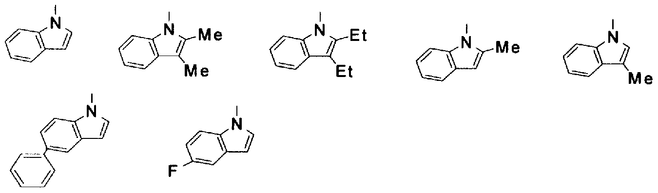


Claims


Priority Applications (3)
| Application Number | Priority Date | Filing Date | Title |
|---|---|---|---|
| JP2006510748A JPWO2005085387A1 (ja) | 2004-03-08 | 2005-03-04 | 有機エレクトロルミネッセンス素子用材料及びそれを利用した有機エレクトロルミネッセンス素子 |
| EP05720055A EP1724323A4 (en) | 2004-03-08 | 2005-03-04 | MATERIAL FOR ORGANIC ELECTROLUMINESCENCE DEVICE AND ORGANIC ELECTROLUMINESCENCE DEVICE USING SUCH MATERIAL |
| US10/591,908 US20070190355A1 (en) | 2004-03-08 | 2005-03-04 | Material for organic electroluminescence device and organic electroluminescence device utilizing the same |
Applications Claiming Priority (2)
| Application Number | Priority Date | Filing Date | Title |
|---|---|---|---|
| JP2004064004 | 2004-03-08 | ||
| JP2004-064004 | 2004-03-08 |
Publications (1)
| Publication Number | Publication Date |
|---|---|
| WO2005085387A1 true WO2005085387A1 (ja) | 2005-09-15 |
Family
ID=34918176
Family Applications (1)
| Application Number | Title | Priority Date | Filing Date |
|---|---|---|---|
| PCT/JP2005/003783 WO2005085387A1 (ja) | 2004-03-08 | 2005-03-04 | 有機エレクトロルミネッセンス素子用材料及びそれを利用した有機エレクトロルミネッセンス素子 |
Country Status (6)
| Country | Link |
|---|---|
| US (1) | US20070190355A1 (ja) |
| EP (1) | EP1724323A4 (ja) |
| JP (1) | JPWO2005085387A1 (ja) |
| CN (1) | CN1934213A (ja) |
| TW (1) | TW200602457A (ja) |
| WO (1) | WO2005085387A1 (ja) |
Cited By (64)
| Publication number | Priority date | Publication date | Assignee | Title |
|---|---|---|---|---|
| WO2006040915A2 (ja) * | 2004-09-22 | 2006-04-20 | Japan Science & Tech Agency | 有機エレクトロルミネッセンス素子 |
| WO2006062062A1 (ja) * | 2004-12-10 | 2006-06-15 | Pioneer Corporation | 有機化合物、電荷輸送材料および有機電界発光素子 |
| WO2006067976A1 (ja) * | 2004-12-24 | 2006-06-29 | Pioneer Corporation | 有機化合物、電荷輸送材料および有機電界発光素子 |
| JP2006188493A (ja) * | 2004-12-10 | 2006-07-20 | Pioneer Electronic Corp | 有機化合物、電荷輸送材料および有機電界発光素子 |
| JP2008214615A (ja) * | 2007-02-06 | 2008-09-18 | Sumitomo Chemical Co Ltd | 組成物及び該組成物を用いてなる発光素子 |
| WO2009031855A1 (en) * | 2007-09-05 | 2009-03-12 | Cheil Industries Inc. | Material for organic photoelectric device, and organic photoelectric device including the same |
| JP2009224512A (ja) * | 2008-03-14 | 2009-10-01 | Tosoh Corp | りん光性の有機電界発光素子 |
| JP2010090084A (ja) * | 2008-10-10 | 2010-04-22 | Chemiprokasei Kaisha Ltd | 新規なビス(カルバゾリルフェニル)誘導体、それを用いたホスト材料および有機エレクトロルミネッセンス素子 |
| WO2010074422A1 (en) * | 2008-12-24 | 2010-07-01 | Cheil Industries Inc. | Novel compound for organic photoelectric device and organic photoelectric device including the same |
| WO2011021689A1 (ja) | 2009-08-21 | 2011-02-24 | 東ソー株式会社 | 環状アジン誘導体とそれらの製造方法、ならびにそれらを構成成分とする有機電界発光素子 |
| JP2011063584A (ja) * | 2009-08-21 | 2011-03-31 | Tosoh Corp | トリアジン誘導体、その製造方法、及びそれを構成成分とする有機電界発光素子 |
| WO2011046182A1 (ja) * | 2009-10-16 | 2011-04-21 | 出光興産株式会社 | 含フルオレン芳香族化合物、有機エレクトロルミネッセンス素子用材料及びそれを用いた有機エレクトロルミネッセンス素子 |
| JP2011084553A (ja) * | 2009-09-15 | 2011-04-28 | Tosoh Corp | ピリミジン誘導体、その製造方法、及びそれを構成成分とする有機電界発光素子 |
| WO2011057706A2 (de) | 2009-11-14 | 2011-05-19 | Merck Patent Gmbh | Materialien für elektronische vorrichtungen |
| JP2011121934A (ja) * | 2009-11-12 | 2011-06-23 | Tosoh Corp | トリアジン誘導体、その製造方法、及びそれを構成成分とする有機電界発光素子 |
| JP4751955B1 (ja) * | 2010-07-09 | 2011-08-17 | 富士フイルム株式会社 | 有機電界発光素子 |
| JP2012501091A (ja) * | 2008-08-25 | 2012-01-12 | チェイル インダストリーズ インコーポレイテッド | 有機光電素子用材料およびこれを含む有機光電素子 |
| JP2012056880A (ja) * | 2010-09-08 | 2012-03-22 | Idemitsu Kosan Co Ltd | インドロカルバゾール化合物、有機エレクトロルミネッセンス素子用材料、及びそれを用いた有機エレクトロルミネッセンス素子 |
| KR20120042886A (ko) | 2009-07-31 | 2012-05-03 | 후지필름 가부시키가이샤 | 유기 전계 발광 소자 |
| WO2012069121A1 (de) | 2010-11-24 | 2012-05-31 | Merck Patent Gmbh | Materialien für organische elektrolumineszenzvorrichtungen |
| WO2012080052A1 (en) | 2010-12-13 | 2012-06-21 | Basf Se | Bispyrimidines for electronic applications |
| WO2012110182A1 (de) | 2011-02-17 | 2012-08-23 | Merck Patent Gmbh | Verbindungen für elektronische vorrichtungen |
| WO2012149999A1 (de) | 2011-05-05 | 2012-11-08 | Merck Patent Gmbh | Verbindungen für elektronische vorrichtungen |
| US8362246B2 (en) | 2010-12-13 | 2013-01-29 | Basf Se | Bispyrimidines for electronic applications |
| WO2013050862A1 (ja) | 2011-10-07 | 2013-04-11 | ユーディーシー アイルランド リミテッド | 有機電界発光素子及び該素子用発光材料並びに発光装置、表示装置及び照明装置 |
| WO2013064881A2 (ja) | 2011-11-02 | 2013-05-10 | ユーディーシー アイルランド リミテッド | 有機電界発光素子、有機電界発光素子用材料並びに該有機電界発光素子を用いた発光装置、表示装置及び照明装置 |
| WO2013069762A1 (ja) * | 2011-11-11 | 2013-05-16 | 東ソー株式会社 | 含窒素縮環芳香族基を有する環状アジン化合物とその製造方法、及びそれを構成成分とする有機電界発光素子 |
| WO2013072740A2 (ja) | 2011-11-15 | 2013-05-23 | ユーディーシー アイルランド リミテッド | 電荷輸送材料、有機電界発光素子及び該素子を用いたことを特徴とする発光装置、表示装置または照明装置 |
| WO2013108069A2 (ja) | 2011-10-06 | 2013-07-25 | ユーディーシー アイルランド リミテッド | 有機電界発光素子とそれに用いることができる化合物および有機電界発光素子用材料、並びに該素子を用いた発光装置、表示装置及び照明装置 |
| EP2623508A1 (en) | 2012-02-02 | 2013-08-07 | Konica Minolta Advanced Layers, Inc. | Iridium complex compound, organic electroluminescent element material, organic electroluminescent element, illumination device and display device |
| DE102013201846A1 (de) | 2012-02-06 | 2013-08-14 | Udc Ireland Limited | Organisches Elektrolumineszenz-Element, Verbindung und Material für organisches Elektrolumineszenz-Element, die hier verrwendet werden können, Licht-emittierende Vorrichtung, Anzeigevorrichtung und Beleuchtungsvorrichtung, die jeweils das Element verwenden |
| WO2014030666A1 (ja) | 2012-08-24 | 2014-02-27 | コニカミノルタ株式会社 | 透明電極、電子デバイス、および透明電極の製造方法 |
| JP2014125449A (ja) * | 2012-12-26 | 2014-07-07 | Tosoh Corp | 環状アジン化合物の製造方法 |
| JP2014139237A (ja) * | 2007-11-30 | 2014-07-31 | Semiconductor Energy Lab Co Ltd | キノキサリン誘導体 |
| WO2014157618A1 (ja) | 2013-03-29 | 2014-10-02 | コニカミノルタ株式会社 | 有機エレクトロルミネッセンス素子、それを具備した照明装置及び表示装置 |
| WO2014157610A1 (ja) | 2013-03-29 | 2014-10-02 | コニカミノルタ株式会社 | 有機エレクトロルミネッセンス素子、照明装置、表示装置、有機ルミネッセンス素子用発光性薄膜と組成物及び発光方法 |
| WO2014157494A1 (ja) | 2013-03-29 | 2014-10-02 | コニカミノルタ株式会社 | 有機エレクトロルミネッセンス素子用材料、有機エレクトロルミネッセンス素子、表示装置及び照明装置 |
| US8933622B2 (en) | 2005-05-24 | 2015-01-13 | Pioneer Corporation | Organic electroluminescence element |
| US9059411B2 (en) | 2012-02-29 | 2015-06-16 | Semiconductor Energy Laboratory Co., Ltd. | Fluorene compound, light-emitting element, light-emitting device, electronic device, and lighting device |
| US9133118B2 (en) | 2010-01-15 | 2015-09-15 | Udc Ireland Limited | Organic electroluminescence device |
| WO2015156449A1 (ko) * | 2014-04-09 | 2015-10-15 | 삼성에스디아이 주식회사 | 유기 화합물, 조성물, 유기 광전자 소자 및 표시 장치 |
| WO2016002864A1 (ja) * | 2014-07-01 | 2016-01-07 | 東ソー株式会社 | トリアジン化合物、その製造方法、及びその用途 |
| JP2016050195A (ja) * | 2014-09-02 | 2016-04-11 | 東ソー株式会社 | トリアジン化合物、その製造方法、及びそれを構成成分とする有機電界発光素子 |
| US9340728B2 (en) | 2009-07-31 | 2016-05-17 | Udc Ireland Limited | Organic electroluminescence device |
| WO2016117429A1 (ja) * | 2015-01-20 | 2016-07-28 | 保土谷化学工業株式会社 | ピリミジン誘導体および有機エレクトロルミネッセンス素子 |
| JP2016155795A (ja) * | 2014-07-01 | 2016-09-01 | 東ソー株式会社 | トリアジン化合物、その製造方法、及びその用途 |
| KR20170015414A (ko) | 2010-01-28 | 2017-02-08 | 유디씨 아일랜드 리미티드 | 유기 전계 발광 소자 및 전하 수송 재료 |
| WO2017043645A1 (ja) * | 2015-09-10 | 2017-03-16 | 東ソー株式会社 | 環状アジン化合物、その製造方法、製造中間体、及び用途 |
| US9663711B2 (en) | 2011-08-25 | 2017-05-30 | Semiconductor Energy Laboratory Co., Ltd. | Light-emitting element, light-emitting device, electronic device, lighting device, and novel organic compound |
| US9676717B2 (en) | 2010-01-15 | 2017-06-13 | Udc Ireland Limited | Organic electroluminescence device |
| KR20170087845A (ko) | 2010-01-28 | 2017-07-31 | 유디씨 아일랜드 리미티드 | 유기 전계 발광 소자 |
| EP3200255A2 (en) | 2016-01-06 | 2017-08-02 | Konica Minolta, Inc. | Organic electroluminescent element, method for producing organic electroluminescent element, display, and lighting device |
| JP2017160145A (ja) * | 2016-03-08 | 2017-09-14 | 東ソー株式会社 | トリアリールトリアジン化合物の製造方法 |
| US20180062085A1 (en) * | 2016-08-24 | 2018-03-01 | Cynora Gmbh | Organic molecules for use in optoelectronic devices |
| US9923149B2 (en) | 2014-05-23 | 2018-03-20 | Semiconductor Energy Laboratory Co., Ltd. | Heterocyclic compound, light-emitting element, light-emitting device, electronic device, and lighting device |
| JP2018534237A (ja) * | 2015-09-11 | 2018-11-22 | エルジー・ケム・リミテッド | ヘテロ環化合物およびこれを用いた有機発光素子 |
| JP2019513133A (ja) * | 2016-03-17 | 2019-05-23 | メルク、パテント、ゲゼルシャフト、ミット、ベシュレンクテル、ハフツングMerck Patent GmbH | スピロビフルオレン構造を有する化合物 |
| US10312454B2 (en) | 2015-06-17 | 2019-06-04 | Samsung Sdi Co., Ltd. | Compound for organic optoelectric device, organic optoelectric device and display device |
| US10431749B2 (en) | 2010-07-09 | 2019-10-01 | Udc Ireland Limited | Organic electroluminescent element |
| US10446764B2 (en) | 2014-05-22 | 2019-10-15 | Samsung Sdi Co., Ltd. | Organic compound, composition, organic optoelectric device, and display device |
| US10644245B2 (en) | 2015-06-19 | 2020-05-05 | Samsung Sdi Co., Ltd. | Composition for organic photoelectronic element, organic photoelectronic element, and display apparatus |
| US10784447B2 (en) | 2015-04-24 | 2020-09-22 | Samsung Sdi Co., Ltd. | Organic compound, composition, and organic optoelectronic diode |
| US11177441B2 (en) | 2014-01-24 | 2021-11-16 | Samsung Sdi Co., Ltd. | Organic compound, composition, organic optoelectronic device, and display device |
| EP4271160A2 (en) | 2015-02-13 | 2023-11-01 | Merck Patent GmbH | Aromatic heterocyclic derivative, and organic electroluminescent element, illumination device, and display device using aromatic heterocyclic derivative |
Families Citing this family (44)
| Publication number | Priority date | Publication date | Assignee | Title |
|---|---|---|---|---|
| EP1750487A4 (en) * | 2004-05-14 | 2008-12-17 | Idemitsu Kosan Co | ORGANIC ELECTROLUMINESCENCE ELEMENT |
| US7651791B2 (en) | 2005-12-15 | 2010-01-26 | Idemitsu Kosan Co., Ltd. | Material for organic electroluminescence device and electroluminescence device employing the same |
| CN110724124A (zh) * | 2007-05-17 | 2020-01-24 | 株式会社半导体能源研究所 | 三唑衍生物 |
| KR100957620B1 (ko) * | 2007-11-01 | 2010-05-13 | 제일모직주식회사 | 유기광전소자용 재료, 및 이를 이용한 유기광전소자 |
| JP2010031248A (ja) * | 2008-06-23 | 2010-02-12 | Sumitomo Chemical Co Ltd | 組成物及び該組成物を用いてなる発光素子 |
| EP2452997A4 (en) * | 2009-07-10 | 2013-10-09 | Cheil Ind Inc | CONNECTION FOR AN ORGANIC PHOTOELECTRIC ELEMENT AND ORGANIC PHOTOELECTRIC ELEMENT THEREWITH |
| US8617720B2 (en) | 2009-12-21 | 2013-12-31 | E I Du Pont De Nemours And Company | Electroactive composition and electronic device made with the composition |
| JP5238889B2 (ja) | 2010-01-15 | 2013-07-17 | 出光興産株式会社 | 有機エレクトロルミネッセンス素子 |
| JP4729642B1 (ja) * | 2010-07-09 | 2011-07-20 | 富士フイルム株式会社 | 有機電界発光素子 |
| US8883323B2 (en) | 2010-11-22 | 2014-11-11 | Idemitsu Kosan Co., Ltd. | Organic electroluminescence device |
| US9324950B2 (en) * | 2010-11-22 | 2016-04-26 | Idemitsu Kosan Co., Ltd. | Organic electroluminescence device |
| US20130264560A1 (en) * | 2010-12-20 | 2013-10-10 | E I Du Pont De Nemours And Company | Triazine derivatives for electronic applications |
| US9705091B2 (en) | 2010-12-20 | 2017-07-11 | Idemitsu Kosan Co., Ltd. | Aromatic heterocycle derivative and organic electroluminescent element using same |
| KR101802008B1 (ko) * | 2010-12-21 | 2017-11-27 | 이 아이 듀폰 디 네모아 앤드 캄파니 | 피리미딘 화합물을 포함하는 전자 소자 |
| KR102261235B1 (ko) | 2011-11-22 | 2021-06-04 | 이데미쓰 고산 가부시키가이샤 | 방향족 복소 고리 유도체, 유기 일렉트로루미네선스 소자용 재료 및 유기 일렉트로루미네선스 소자 |
| EP2752902B9 (en) | 2011-11-22 | 2017-08-30 | Idemitsu Kosan Co., Ltd | Aromatic heterocyclic derivative, material for organic electroluminescent element, and organic electroluminescent element |
| KR101407588B1 (ko) | 2011-12-27 | 2014-06-13 | 에스에프씨 주식회사 | 축합환 화합물 및 이를 포함한 유기 발광 소자 |
| CN103360368A (zh) * | 2012-03-30 | 2013-10-23 | 海洋王照明科技股份有限公司 | 含苯并咪唑取代吡啶的有机半导体材料及其制备方法和应用 |
| JP6312960B2 (ja) | 2012-08-03 | 2018-04-18 | 株式会社半導体エネルギー研究所 | 発光素子、発光装置、電子機器、照明装置及び複素環化合物 |
| KR102176965B1 (ko) * | 2012-09-07 | 2020-11-10 | 이데미쓰 고산 가부시키가이샤 | 신규 방향족 복소 고리 유도체, 유기 일렉트로 루미네선스 소자용 재료, 유기 일렉트로 루미네선스 소자용 재료 용액 및 유기 일렉트로 루미네선스 소자 |
| EP2896621B1 (en) * | 2012-09-12 | 2018-04-25 | Idemitsu Kosan Co., Ltd | Novel compound, material for organic electroluminescence element, organic electroluminescence element, and electronic device |
| KR101499356B1 (ko) * | 2013-06-28 | 2015-03-05 | 주식회사 엘지화학 | 헤테로환 화합물 및 이를 포함하는 유기 발광 소자 |
| CN105473569B (zh) | 2013-11-13 | 2021-01-01 | 出光兴产株式会社 | 化合物、有机电致发光元件用材料、有机电致发光元件和电子设备 |
| KR102235598B1 (ko) * | 2014-03-11 | 2021-04-05 | 삼성디스플레이 주식회사 | 축합환 화합물 및 이를 포함하는 유기 전계 발광 소자 |
| KR101542714B1 (ko) | 2014-04-04 | 2015-08-12 | 주식회사 엘지화학 | 헤테로고리 화합물 및 이를 포함하는 유기 발광 소자 |
| KR101537500B1 (ko) | 2014-04-04 | 2015-07-20 | 주식회사 엘지화학 | 유기 발광 소자 |
| KR20150115622A (ko) | 2014-04-04 | 2015-10-14 | 주식회사 엘지화학 | 헤테로고리 화합물 및 이를 포함하는 유기 발광 소자 |
| CN103951657A (zh) * | 2014-05-09 | 2014-07-30 | 江西冠能光电材料有限公司 | 一种高电负性有机半导体 |
| US10297762B2 (en) * | 2014-07-09 | 2019-05-21 | Universal Display Corporation | Organic electroluminescent materials and devices |
| KR101857146B1 (ko) * | 2014-10-28 | 2018-05-11 | 삼성에스디아이 주식회사 | 유기 광전자 소자 및 표시 장치 |
| KR101829749B1 (ko) * | 2014-10-31 | 2018-02-19 | 삼성에스디아이 주식회사 | 유기 광전자 소자용 화합물, 유기 광전자 소자용 조성물, 유기 광전자 소자 및 표시 장치 |
| CN105646458A (zh) * | 2014-11-13 | 2016-06-08 | 上海和辉光电有限公司 | 一种化合物及其制备方法和应用 |
| CN105646459A (zh) * | 2014-11-13 | 2016-06-08 | 上海和辉光电有限公司 | 一种化合物及其制备方法和应用 |
| JP6640735B2 (ja) | 2014-11-28 | 2020-02-05 | 出光興産株式会社 | 化合物、有機エレクトロルミネッセンス素子用材料、有機エレクトロルミネッセンス素子および電子機器 |
| KR102611317B1 (ko) | 2014-12-24 | 2023-12-07 | 솔루스첨단소재 주식회사 | 유기 화합물 및 이를 포함하는 유기 전계 발광 소자 |
| KR101924086B1 (ko) * | 2016-02-26 | 2018-11-30 | 삼성에스디아이 주식회사 | 유기 화합물, 유기 광전자 소자 및 표시 장치 |
| KR101999709B1 (ko) * | 2016-03-21 | 2019-07-12 | 주식회사 엘지화학 | 유기 발광 소자 |
| KR102044942B1 (ko) * | 2016-05-02 | 2019-11-14 | 삼성에스디아이 주식회사 | 유기 광전자 소자용 화합물, 유기 광전자 소자 및 표시 장치 |
| CN110511212B (zh) * | 2019-09-12 | 2021-10-19 | 南京邮电大学 | 一种双极性d-a型主体材料及有机电致发光器件 |
| CN111205269B (zh) * | 2020-01-10 | 2023-05-12 | 上海百豪新材料有限公司 | 基于咔唑的有机电致磷光材料组成物制备方法及应用制备 |
| CN111187254B (zh) * | 2020-01-10 | 2023-11-07 | 上海百豪新材料有限公司 | 一种基于咔唑的有机电致磷光材料组成物及其应用 |
| US20230124891A1 (en) * | 2020-02-05 | 2023-04-20 | Idemitsu Kosan Co.,Ltd. | Compound, material for organic electroluminescent elements, organic electroluminescent element, and electronic device |
| CN117177967A (zh) * | 2022-03-21 | 2023-12-05 | 株式会社Lg化学 | 含杂环的化合物和包含其的有机发光器件 |
| KR20230173757A (ko) * | 2022-06-17 | 2023-12-27 | 덕산네오룩스 주식회사 | 유기전기소자용 화합물, 이를 이용한 유기전기소자 및 그 전자 장치 |
Citations (2)
| Publication number | Priority date | Publication date | Assignee | Title |
|---|---|---|---|---|
| JP2003022893A (ja) * | 2001-07-06 | 2003-01-24 | Fuji Photo Film Co Ltd | 発光素子 |
| JP2004022334A (ja) * | 2002-06-17 | 2004-01-22 | Konica Minolta Holdings Inc | 有機エレクトロルミネッセンス素子及び表示装置 |
Family Cites Families (4)
| Publication number | Priority date | Publication date | Assignee | Title |
|---|---|---|---|---|
| JP4036041B2 (ja) * | 2002-06-24 | 2008-01-23 | コニカミノルタホールディングス株式会社 | 有機エレクトロルミネッセンス素子及び表示装置 |
| JP4490923B2 (ja) * | 2003-12-15 | 2010-06-30 | 出光興産株式会社 | 有機エレクトロルミネッセンス素子用材料及びそれを用いた有機エレクロルミネッセンス素子 |
| TWI428053B (zh) * | 2004-02-09 | 2014-02-21 | Idemitsu Kosan Co | Organic electroluminescent element |
| TW200541401A (en) * | 2004-02-13 | 2005-12-16 | Idemitsu Kosan Co | Organic electroluminescent device |
-
2005
- 2005-03-04 US US10/591,908 patent/US20070190355A1/en not_active Abandoned
- 2005-03-04 CN CNA2005800075331A patent/CN1934213A/zh active Pending
- 2005-03-04 JP JP2006510748A patent/JPWO2005085387A1/ja not_active Withdrawn
- 2005-03-04 EP EP05720055A patent/EP1724323A4/en not_active Withdrawn
- 2005-03-04 WO PCT/JP2005/003783 patent/WO2005085387A1/ja active Application Filing
- 2005-03-08 TW TW094107036A patent/TW200602457A/zh unknown
Patent Citations (2)
| Publication number | Priority date | Publication date | Assignee | Title |
|---|---|---|---|---|
| JP2003022893A (ja) * | 2001-07-06 | 2003-01-24 | Fuji Photo Film Co Ltd | 発光素子 |
| JP2004022334A (ja) * | 2002-06-17 | 2004-01-22 | Konica Minolta Holdings Inc | 有機エレクトロルミネッセンス素子及び表示装置 |
Non-Patent Citations (1)
| Title |
|---|
| See also references of EP1724323A4 * |
Cited By (107)
| Publication number | Priority date | Publication date | Assignee | Title |
|---|---|---|---|---|
| WO2006040915A3 (ja) * | 2004-09-22 | 2006-06-29 | Japan Science & Tech Agency | 有機エレクトロルミネッセンス素子 |
| WO2006040915A2 (ja) * | 2004-09-22 | 2006-04-20 | Japan Science & Tech Agency | 有機エレクトロルミネッセンス素子 |
| EP1820801A4 (en) * | 2004-12-10 | 2009-12-23 | Pioneer Corp | ORGANIC COMPOUND, CHARGE TRANSPORT MATERIAL, AND ORGANIC ELECTROLUMINESCENT ELEMENT |
| JP2006188493A (ja) * | 2004-12-10 | 2006-07-20 | Pioneer Electronic Corp | 有機化合物、電荷輸送材料および有機電界発光素子 |
| WO2006062062A1 (ja) * | 2004-12-10 | 2006-06-15 | Pioneer Corporation | 有機化合物、電荷輸送材料および有機電界発光素子 |
| US8178215B2 (en) | 2004-12-10 | 2012-05-15 | Pioneer Corporation | Organic compound containing at least two carbazolyl-substituted phenyl structures; charge-transporting material and organic el element containing the compound |
| WO2006067976A1 (ja) * | 2004-12-24 | 2006-06-29 | Pioneer Corporation | 有機化合物、電荷輸送材料および有機電界発光素子 |
| JP2006199679A (ja) * | 2004-12-24 | 2006-08-03 | Pioneer Electronic Corp | 有機化合物、電荷輸送材料および有機電界発光素子 |
| US8324403B2 (en) | 2004-12-24 | 2012-12-04 | Pioneer Corporation | Organic compound, charge-transporting material, and organic electroluminescent element |
| US8933622B2 (en) | 2005-05-24 | 2015-01-13 | Pioneer Corporation | Organic electroluminescence element |
| JP2008214615A (ja) * | 2007-02-06 | 2008-09-18 | Sumitomo Chemical Co Ltd | 組成物及び該組成物を用いてなる発光素子 |
| WO2009031855A1 (en) * | 2007-09-05 | 2009-03-12 | Cheil Industries Inc. | Material for organic photoelectric device, and organic photoelectric device including the same |
| US8343640B2 (en) | 2007-09-05 | 2013-01-01 | Cheil Industries, Inc. | Material for organic photoelectric device, and organic photoelectric device including the same |
| US9595677B2 (en) | 2007-09-05 | 2017-03-14 | Cheil Industries, Inc. | Material for organic photoelectric device, and organic photoelectric device including the same |
| JP2014139237A (ja) * | 2007-11-30 | 2014-07-31 | Semiconductor Energy Lab Co Ltd | キノキサリン誘導体 |
| JP2009224512A (ja) * | 2008-03-14 | 2009-10-01 | Tosoh Corp | りん光性の有機電界発光素子 |
| JP2012501091A (ja) * | 2008-08-25 | 2012-01-12 | チェイル インダストリーズ インコーポレイテッド | 有機光電素子用材料およびこれを含む有機光電素子 |
| JP2010090084A (ja) * | 2008-10-10 | 2010-04-22 | Chemiprokasei Kaisha Ltd | 新規なビス(カルバゾリルフェニル)誘導体、それを用いたホスト材料および有機エレクトロルミネッセンス素子 |
| JP2012513987A (ja) * | 2008-12-24 | 2012-06-21 | チェイル インダストリーズ インコーポレイテッド | 新規な有機光電素子用化合物およびこれを含む有機光電素子 |
| US9199966B2 (en) | 2008-12-24 | 2015-12-01 | Cheil Industries, Inc. | Compound for an organic photoelectric device, organic photoelectric device, and display device including the same |
| WO2010074422A1 (en) * | 2008-12-24 | 2010-07-01 | Cheil Industries Inc. | Novel compound for organic photoelectric device and organic photoelectric device including the same |
| US9340728B2 (en) | 2009-07-31 | 2016-05-17 | Udc Ireland Limited | Organic electroluminescence device |
| KR20120042886A (ko) | 2009-07-31 | 2012-05-03 | 후지필름 가부시키가이샤 | 유기 전계 발광 소자 |
| KR20170038117A (ko) | 2009-07-31 | 2017-04-05 | 유디씨 아일랜드 리미티드 | 유기 전계 발광 소자 |
| KR20180015771A (ko) | 2009-07-31 | 2018-02-13 | 유디씨 아일랜드 리미티드 | 유기 전계 발광 소자 |
| EP3389110A1 (en) | 2009-07-31 | 2018-10-17 | UDC Ireland Limited | Organic electroluminescent element |
| EP4326036A2 (en) | 2009-07-31 | 2024-02-21 | UDC Ireland Limited | Organic electroluminescent element |
| KR20170120193A (ko) | 2009-07-31 | 2017-10-30 | 유디씨 아일랜드 리미티드 | 유기 전계 발광 소자 |
| US9120773B2 (en) | 2009-08-21 | 2015-09-01 | Tosoh Corporation | Cyclic azine derivatives, processes for producing these, and organic electroluminescent element containing these as component |
| US9624193B2 (en) | 2009-08-21 | 2017-04-18 | Tosoh Corporation | Cyclic azine derivatives, processes for producing these, and organic electroluminescent element containing these as component |
| WO2011021689A1 (ja) | 2009-08-21 | 2011-02-24 | 東ソー株式会社 | 環状アジン誘導体とそれらの製造方法、ならびにそれらを構成成分とする有機電界発光素子 |
| JP2011063584A (ja) * | 2009-08-21 | 2011-03-31 | Tosoh Corp | トリアジン誘導体、その製造方法、及びそれを構成成分とする有機電界発光素子 |
| JP2011084553A (ja) * | 2009-09-15 | 2011-04-28 | Tosoh Corp | ピリミジン誘導体、その製造方法、及びそれを構成成分とする有機電界発光素子 |
| CN102471320A (zh) * | 2009-10-16 | 2012-05-23 | 出光兴产株式会社 | 含芴芳香族化合物、有机电致发光元件用材料及使用其的有机电致发光元件 |
| WO2011046182A1 (ja) * | 2009-10-16 | 2011-04-21 | 出光興産株式会社 | 含フルオレン芳香族化合物、有機エレクトロルミネッセンス素子用材料及びそれを用いた有機エレクトロルミネッセンス素子 |
| EP2489664A4 (en) * | 2009-10-16 | 2013-04-03 | Idemitsu Kosan Co | AROMATIC COMPOUND CONTAINING FLUORENE, MATERIAL FOR ORGANIC ELECTROLUMINESCENCE ELEMENT, AND ORGANIC ELECTROLUMINESCENT ELEMENT USING SUCH MATERIAL |
| US9266851B2 (en) | 2009-10-16 | 2016-02-23 | Idemitsu Kosan Co., Ltd. | Fluorene-containing aromatic compound, material for organic electroluminescent element, and organic electroluminescent element using same |
| JP2011121934A (ja) * | 2009-11-12 | 2011-06-23 | Tosoh Corp | トリアジン誘導体、その製造方法、及びそれを構成成分とする有機電界発光素子 |
| WO2011057706A2 (de) | 2009-11-14 | 2011-05-19 | Merck Patent Gmbh | Materialien für elektronische vorrichtungen |
| DE102009053382A1 (de) | 2009-11-14 | 2011-05-19 | Merck Patent Gmbh | Materialien für elektronische Vorrichtungen |
| US9676717B2 (en) | 2010-01-15 | 2017-06-13 | Udc Ireland Limited | Organic electroluminescence device |
| US9133118B2 (en) | 2010-01-15 | 2015-09-15 | Udc Ireland Limited | Organic electroluminescence device |
| KR20170015414A (ko) | 2010-01-28 | 2017-02-08 | 유디씨 아일랜드 리미티드 | 유기 전계 발광 소자 및 전하 수송 재료 |
| KR20170087845A (ko) | 2010-01-28 | 2017-07-31 | 유디씨 아일랜드 리미티드 | 유기 전계 발광 소자 |
| KR20170092138A (ko) | 2010-01-28 | 2017-08-10 | 유디씨 아일랜드 리미티드 | 유기 전계 발광 소자 및 전하 수송 재료 |
| JP4751955B1 (ja) * | 2010-07-09 | 2011-08-17 | 富士フイルム株式会社 | 有機電界発光素子 |
| US10431749B2 (en) | 2010-07-09 | 2019-10-01 | Udc Ireland Limited | Organic electroluminescent element |
| JP2012056880A (ja) * | 2010-09-08 | 2012-03-22 | Idemitsu Kosan Co Ltd | インドロカルバゾール化合物、有機エレクトロルミネッセンス素子用材料、及びそれを用いた有機エレクトロルミネッセンス素子 |
| WO2012069121A1 (de) | 2010-11-24 | 2012-05-31 | Merck Patent Gmbh | Materialien für organische elektrolumineszenzvorrichtungen |
| JP2014507383A (ja) * | 2010-12-13 | 2014-03-27 | ビーエーエスエフ ソシエタス・ヨーロピア | 電子装置用途のためのビスピリミジン |
| US8362246B2 (en) | 2010-12-13 | 2013-01-29 | Basf Se | Bispyrimidines for electronic applications |
| JP2016183190A (ja) * | 2010-12-13 | 2016-10-20 | ビーエーエスエフ ソシエタス・ヨーロピアBasf Se | 電子装置用途のためのビスピリミジン |
| WO2012080052A1 (en) | 2010-12-13 | 2012-06-21 | Basf Se | Bispyrimidines for electronic applications |
| WO2012110182A1 (de) | 2011-02-17 | 2012-08-23 | Merck Patent Gmbh | Verbindungen für elektronische vorrichtungen |
| WO2012149999A1 (de) | 2011-05-05 | 2012-11-08 | Merck Patent Gmbh | Verbindungen für elektronische vorrichtungen |
| US11008510B2 (en) | 2011-08-25 | 2021-05-18 | Semiconductor Energy Laboratory Co., Ltd. | Light-emitting element, light-emitting device, electronic device, lighting device, and novel organic compound |
| US11773321B2 (en) | 2011-08-25 | 2023-10-03 | Semiconductor Energy Laboratory Co., Ltd. | Light-emitting element, light-emitting device, electronic device, lighting device, and novel organic compound |
| US9663711B2 (en) | 2011-08-25 | 2017-05-30 | Semiconductor Energy Laboratory Co., Ltd. | Light-emitting element, light-emitting device, electronic device, lighting device, and novel organic compound |
| WO2013108069A2 (ja) | 2011-10-06 | 2013-07-25 | ユーディーシー アイルランド リミテッド | 有機電界発光素子とそれに用いることができる化合物および有機電界発光素子用材料、並びに該素子を用いた発光装置、表示装置及び照明装置 |
| WO2013050862A1 (ja) | 2011-10-07 | 2013-04-11 | ユーディーシー アイルランド リミテッド | 有機電界発光素子及び該素子用発光材料並びに発光装置、表示装置及び照明装置 |
| WO2013064881A2 (ja) | 2011-11-02 | 2013-05-10 | ユーディーシー アイルランド リミテッド | 有機電界発光素子、有機電界発光素子用材料並びに該有機電界発光素子を用いた発光装置、表示装置及び照明装置 |
| CN104039773B (zh) * | 2011-11-11 | 2016-08-24 | 东曹株式会社 | 具有含氮缩环芳香基的环状吖嗪化合物及其制造方法、以及以该环状吖嗪化合物为构成成分的有机电致发光元件 |
| US9252368B2 (en) | 2011-11-11 | 2016-02-02 | Tosoh Corporation | Cyclic azine compound having nitrogen-containing condensed aromatic group, method for producing same, and organic electroluminescent device comprising same as constituent component |
| CN104039773A (zh) * | 2011-11-11 | 2014-09-10 | 东曹株式会社 | 具有含氮缩环芳香基的环状吖嗪化合物及其制造方法、以及以该环状吖嗪化合物为构成成分的有机电致发光元件 |
| JP2014111548A (ja) * | 2011-11-11 | 2014-06-19 | Tosoh Corp | 含窒素縮環芳香族基を有する環状アジン化合物とその製造方法、及びそれらを構成成分とする有機電界発光素子 |
| WO2013069762A1 (ja) * | 2011-11-11 | 2013-05-16 | 東ソー株式会社 | 含窒素縮環芳香族基を有する環状アジン化合物とその製造方法、及びそれを構成成分とする有機電界発光素子 |
| WO2013072740A2 (ja) | 2011-11-15 | 2013-05-23 | ユーディーシー アイルランド リミテッド | 電荷輸送材料、有機電界発光素子及び該素子を用いたことを特徴とする発光装置、表示装置または照明装置 |
| EP2623508A1 (en) | 2012-02-02 | 2013-08-07 | Konica Minolta Advanced Layers, Inc. | Iridium complex compound, organic electroluminescent element material, organic electroluminescent element, illumination device and display device |
| DE102013201846A1 (de) | 2012-02-06 | 2013-08-14 | Udc Ireland Limited | Organisches Elektrolumineszenz-Element, Verbindung und Material für organisches Elektrolumineszenz-Element, die hier verrwendet werden können, Licht-emittierende Vorrichtung, Anzeigevorrichtung und Beleuchtungsvorrichtung, die jeweils das Element verwenden |
| DE102013201846B4 (de) | 2012-02-06 | 2021-09-09 | Udc Ireland Limited | Organisches Elektrolumineszenz-Element, Verbindung für organisches Elektrolumineszenz-Element, die hier verwendet werden kann, Licht-emittierende Vorrichtung, Anzeigevorrichtung und Beleuchtungsvorrichtung, die jeweils das Element verwenden |
| US9059411B2 (en) | 2012-02-29 | 2015-06-16 | Semiconductor Energy Laboratory Co., Ltd. | Fluorene compound, light-emitting element, light-emitting device, electronic device, and lighting device |
| WO2014030666A1 (ja) | 2012-08-24 | 2014-02-27 | コニカミノルタ株式会社 | 透明電極、電子デバイス、および透明電極の製造方法 |
| JP2014125449A (ja) * | 2012-12-26 | 2014-07-07 | Tosoh Corp | 環状アジン化合物の製造方法 |
| WO2014157494A1 (ja) | 2013-03-29 | 2014-10-02 | コニカミノルタ株式会社 | 有機エレクトロルミネッセンス素子用材料、有機エレクトロルミネッセンス素子、表示装置及び照明装置 |
| WO2014157618A1 (ja) | 2013-03-29 | 2014-10-02 | コニカミノルタ株式会社 | 有機エレクトロルミネッセンス素子、それを具備した照明装置及び表示装置 |
| WO2014157610A1 (ja) | 2013-03-29 | 2014-10-02 | コニカミノルタ株式会社 | 有機エレクトロルミネッセンス素子、照明装置、表示装置、有機ルミネッセンス素子用発光性薄膜と組成物及び発光方法 |
| US11177441B2 (en) | 2014-01-24 | 2021-11-16 | Samsung Sdi Co., Ltd. | Organic compound, composition, organic optoelectronic device, and display device |
| US10873033B2 (en) | 2014-04-09 | 2020-12-22 | Samsung Sdi Co., Ltd. | Organic compound, composition, organic optoelectronic diode, and display device |
| WO2015156449A1 (ko) * | 2014-04-09 | 2015-10-15 | 삼성에스디아이 주식회사 | 유기 화합물, 조성물, 유기 광전자 소자 및 표시 장치 |
| US10446764B2 (en) | 2014-05-22 | 2019-10-15 | Samsung Sdi Co., Ltd. | Organic compound, composition, organic optoelectric device, and display device |
| US10770660B2 (en) | 2014-05-23 | 2020-09-08 | Semiconductor Energy Laboratory Co., Ltd. | Heterocyclic compound, light-emitting element, light-emitting device, electronic device, and lighting device |
| US9923149B2 (en) | 2014-05-23 | 2018-03-20 | Semiconductor Energy Laboratory Co., Ltd. | Heterocyclic compound, light-emitting element, light-emitting device, electronic device, and lighting device |
| WO2016002864A1 (ja) * | 2014-07-01 | 2016-01-07 | 東ソー株式会社 | トリアジン化合物、その製造方法、及びその用途 |
| JP2016155795A (ja) * | 2014-07-01 | 2016-09-01 | 東ソー株式会社 | トリアジン化合物、その製造方法、及びその用途 |
| JP2016050195A (ja) * | 2014-09-02 | 2016-04-11 | 東ソー株式会社 | トリアジン化合物、その製造方法、及びそれを構成成分とする有機電界発光素子 |
| JPWO2016117429A1 (ja) * | 2015-01-20 | 2017-11-09 | 保土谷化学工業株式会社 | ピリミジン誘導体および有機エレクトロルミネッセンス素子 |
| CN107406415A (zh) * | 2015-01-20 | 2017-11-28 | 保土谷化学工业株式会社 | 嘧啶衍生物和有机电致发光器件 |
| WO2016117429A1 (ja) * | 2015-01-20 | 2016-07-28 | 保土谷化学工業株式会社 | ピリミジン誘導体および有機エレクトロルミネッセンス素子 |
| CN107406415B (zh) * | 2015-01-20 | 2021-02-19 | 保土谷化学工业株式会社 | 嘧啶衍生物和有机电致发光器件 |
| US10566543B2 (en) | 2015-01-20 | 2020-02-18 | Hodogaya Chemical Co., Ltd. | Pyrimidine derivative and organic electroluminescent devices |
| EP4271160A2 (en) | 2015-02-13 | 2023-11-01 | Merck Patent GmbH | Aromatic heterocyclic derivative, and organic electroluminescent element, illumination device, and display device using aromatic heterocyclic derivative |
| US10784447B2 (en) | 2015-04-24 | 2020-09-22 | Samsung Sdi Co., Ltd. | Organic compound, composition, and organic optoelectronic diode |
| US10312454B2 (en) | 2015-06-17 | 2019-06-04 | Samsung Sdi Co., Ltd. | Compound for organic optoelectric device, organic optoelectric device and display device |
| US10644245B2 (en) | 2015-06-19 | 2020-05-05 | Samsung Sdi Co., Ltd. | Composition for organic photoelectronic element, organic photoelectronic element, and display apparatus |
| WO2017043645A1 (ja) * | 2015-09-10 | 2017-03-16 | 東ソー株式会社 | 環状アジン化合物、その製造方法、製造中間体、及び用途 |
| JP2017128561A (ja) * | 2015-09-10 | 2017-07-27 | 東ソー株式会社 | 環状アジン化合物、その製造方法、製造中間体、及び用途 |
| JP2018534237A (ja) * | 2015-09-11 | 2018-11-22 | エルジー・ケム・リミテッド | ヘテロ環化合物およびこれを用いた有機発光素子 |
| US10323006B2 (en) | 2015-09-11 | 2019-06-18 | Lg Chem, Ltd. | Heterocyclic compound and organic light emitting element using same |
| EP3200255A2 (en) | 2016-01-06 | 2017-08-02 | Konica Minolta, Inc. | Organic electroluminescent element, method for producing organic electroluminescent element, display, and lighting device |
| JP2017160145A (ja) * | 2016-03-08 | 2017-09-14 | 東ソー株式会社 | トリアリールトリアジン化合物の製造方法 |
| JP7073267B2 (ja) | 2016-03-17 | 2022-05-23 | メルク パテント ゲゼルシャフト ミット ベシュレンクテル ハフツング | スピロビフルオレン構造を有する化合物 |
| JP2019513133A (ja) * | 2016-03-17 | 2019-05-23 | メルク、パテント、ゲゼルシャフト、ミット、ベシュレンクテル、ハフツングMerck Patent GmbH | スピロビフルオレン構造を有する化合物 |
| CN107778294B (zh) * | 2016-08-24 | 2021-07-09 | 西诺拉股份有限公司 | 有机分子,特别应用于有机光电装置中 |
| CN107778294A (zh) * | 2016-08-24 | 2018-03-09 | 西诺拉股份有限公司 | 有机分子,特别应用于有机光电装置中 |
| US11588114B2 (en) | 2016-08-24 | 2023-02-21 | Samsung Display Co., Ltd. | Organic molecules for use in optoelectronic devices |
| US20180062085A1 (en) * | 2016-08-24 | 2018-03-01 | Cynora Gmbh | Organic molecules for use in optoelectronic devices |
| US10665792B2 (en) * | 2016-08-24 | 2020-05-26 | Cynora Gmbh | Organic molecules for use in optoelectronic devices |
Also Published As
| Publication number | Publication date |
|---|---|
| US20070190355A1 (en) | 2007-08-16 |
| TW200602457A (en) | 2006-01-16 |
| CN1934213A (zh) | 2007-03-21 |
| JPWO2005085387A1 (ja) | 2007-12-13 |
| EP1724323A4 (en) | 2008-11-05 |
| EP1724323A1 (en) | 2006-11-22 |
Similar Documents
| Publication | Publication Date | Title |
|---|---|---|
| WO2005085387A1 (ja) | 有機エレクトロルミネッセンス素子用材料及びそれを利用した有機エレクトロルミネッセンス素子 | |
| KR101888249B1 (ko) | 화합물 및 이를 포함하는 유기 전자 소자 | |
| JP5390728B1 (ja) | ビスカルバゾール誘導体、有機エレクトロルミネッセンス素子用材料及びそれを用いた有機エレクトロルミネッセンス素子 | |
| JP6129075B2 (ja) | ビスカルバゾール誘導体およびこれを用いた有機エレクトロルミネッセンス素子 | |
| JP6101248B2 (ja) | 新規化合物、有機エレクトロルミネッセンス素子用材料および有機エレクトロルミネッセンス素子 | |
| KR101290027B1 (ko) | 질소 함유 헤테로환 유도체 및 그것을 사용한 유기전기발광 소자 | |
| TWI471405B (zh) | A phosphorescent element material, and an organic electroluminescent device using the same | |
| TWI551602B (zh) | 具有吲哚并咔唑環結構之化合物及有機電致發光元件 | |
| WO2005112519A1 (ja) | 有機エレクトロルミネッセンス素子 | |
| US20120091885A1 (en) | Novel organic electroluminescent compounds and organic electroluminescent device using the same | |
| JP6060095B2 (ja) | カルバゾール化合物、有機エレクトロルミネッセンス素子用材料および有機エレクトロルミネッセンス素子 | |
| WO2013147205A1 (ja) | 有機エレクトロルミネッセンス素子および有機エレクトロルミネッセンス素子用材料 | |
| EP2110376A1 (en) | Novel compounds for electronic material and organic electronic device using the same | |
| KR20150030660A (ko) | Oled 발광 영역을 위한 비스카바졸 유도체 호스트 물질 및 적색 에미터 | |
| TW200922904A (en) | Phenanthrene derivative and material for organic electroluminescence device | |
| JP2013526014A (ja) | 新規有機電界発光化合物およびこれを使用する有機電界発光素子 | |
| TW201219539A (en) | Monoamine derivative and organic electroluminescent element using same | |
| KR20070030759A (ko) | 유기 전기 발광 소자용 재료 및 이를 이용한 유기 전기발광 소자 | |
| TW200806635A (en) | Nitrogen-containing heterocyclic derivatives and organic electroluminescence device using the same | |
| JP6034005B2 (ja) | ビスカルバゾール誘導体およびこれを用いた有機エレクトロルミネッセンス素子 | |
| EP2372804B1 (en) | Organic electroluminescence element and compound | |
| TW202030193A (zh) | 具有氮雜苯并㗁唑環構造之化合物及有機電致發光元件 | |
| WO2009084544A1 (ja) | 含窒素複素環誘導体及びそれを用いた有機エレクトロルミネッセンス素子 | |
| JP2015013807A (ja) | 芳香族アミン誘導体およびそれを用いた有機エレクトロルミネッセンス素子 |
Legal Events
| Date | Code | Title | Description |
|---|---|---|---|
| AK | Designated states |
Kind code of ref document: A1 Designated state(s): AE AG AL AM AT AU AZ BA BB BG BR BW BY BZ CA CH CN CO CR CU CZ DE DK DM DZ EC EE EG ES FI GB GD GE GH GM HR HU ID IL IN IS JP KE KG KP KR KZ LC LK LR LS LT LU LV MA MD MG MK MN MW MX MZ NA NI NO NZ OM PG PH PL PT RO RU SC SD SE SG SK SL SM SY TJ TM TN TR TT TZ UA UG US UZ VC VN YU ZA ZM ZW |
|
| AL | Designated countries for regional patents |
Kind code of ref document: A1 Designated state(s): BW GH GM KE LS MW MZ NA SD SL SZ TZ UG ZM ZW AM AZ BY KG KZ MD RU TJ TM AT BE BG CH CY CZ DE DK EE ES FI FR GB GR HU IE IS IT LT LU MC NL PL PT RO SE SI SK TR BF BJ CF CG CI CM GA GN GQ GW ML MR NE SN TD TG |
|
| 121 | Ep: the epo has been informed by wipo that ep was designated in this application | ||
| WWE | Wipo information: entry into national phase |
Ref document number: 2006510748 Country of ref document: JP |
|
| WWE | Wipo information: entry into national phase |
Ref document number: 2005720055 Country of ref document: EP |
|
| WWE | Wipo information: entry into national phase |
Ref document number: 3250/CHENP/2006 Country of ref document: IN |
|
| WWE | Wipo information: entry into national phase |
Ref document number: 200580007533.1 Country of ref document: CN Ref document number: 1020067018427 Country of ref document: KR |
|
| NENP | Non-entry into the national phase |
Ref country code: DE |
|
| WWW | Wipo information: withdrawn in national office |
Ref document number: DE |
|
| WWP | Wipo information: published in national office |
Ref document number: 2005720055 Country of ref document: EP |
|
| WWE | Wipo information: entry into national phase |
Ref document number: 10591908 Country of ref document: US Ref document number: 2007190355 Country of ref document: US |
|
| WWP | Wipo information: published in national office |
Ref document number: 1020067018427 Country of ref document: KR |
|
| WWP | Wipo information: published in national office |
Ref document number: 10591908 Country of ref document: US |