US8324403B2 - Organic compound, charge-transporting material, and organic electroluminescent element - Google Patents
Organic compound, charge-transporting material, and organic electroluminescent element Download PDFInfo
- Publication number
- US8324403B2 US8324403B2 US11/722,760 US72276005A US8324403B2 US 8324403 B2 US8324403 B2 US 8324403B2 US 72276005 A US72276005 A US 72276005A US 8324403 B2 US8324403 B2 US 8324403B2
- Authority
- US
- United States
- Prior art keywords
- group
- ring
- organic
- organic compound
- light
- Prior art date
- Legal status (The legal status is an assumption and is not a legal conclusion. Google has not performed a legal analysis and makes no representation as to the accuracy of the status listed.)
- Active, expires
Links
- 0 Cc1cc(-c2ccc(*(c3c-4cccc3)c3ccccc3)c-4c2)ccc1-c1cc(-c2ccccc2*2c3ccccc3)c2cc1 Chemical compound Cc1cc(-c2ccc(*(c3c-4cccc3)c3ccccc3)c-4c2)ccc1-c1cc(-c2ccccc2*2c3ccccc3)c2cc1 0.000 description 11
- LWSYSCQGRROTHV-UHFFFAOYSA-N CC.CCC Chemical compound CC.CCC LWSYSCQGRROTHV-UHFFFAOYSA-N 0.000 description 6
- OTMSDBZUPAUEDD-UHFFFAOYSA-N CC Chemical compound CC OTMSDBZUPAUEDD-UHFFFAOYSA-N 0.000 description 4
- PHKRQYLYOWOUDX-UHFFFAOYSA-N C.C.CC Chemical compound C.C.CC PHKRQYLYOWOUDX-UHFFFAOYSA-N 0.000 description 3
- WPIOAQCLFQJPJT-UHFFFAOYSA-N C1=CC=C(C2=CC(C3=CC(C4=C(N5C6=C(C=CC=C6)C6=C5C=CC=C6)C=CC(N5C6=C(C=CC=C6)C6=C5C=CC=C6)=C4)=CC=C3)=CC(C3=CC=CC=C3)=N2)C=C1 Chemical compound C1=CC=C(C2=CC(C3=CC(C4=C(N5C6=C(C=CC=C6)C6=C5C=CC=C6)C=CC(N5C6=C(C=CC=C6)C6=C5C=CC=C6)=C4)=CC=C3)=CC(C3=CC=CC=C3)=N2)C=C1 WPIOAQCLFQJPJT-UHFFFAOYSA-N 0.000 description 3
- IPEDTLYZERPFFQ-UHFFFAOYSA-N C1=CC=C(C2=CC(C3=CC=C(C4=C(N5C6=C(C=CC=C6)C6=C5C=CC=C6)C=CC(N5C6=C(C=CC=C6)C6=C5C=CC=C6)=C4)C=C3)=CC(C3=CC=CC=C3)=N2)C=C1 Chemical compound C1=CC=C(C2=CC(C3=CC=C(C4=C(N5C6=C(C=CC=C6)C6=C5C=CC=C6)C=CC(N5C6=C(C=CC=C6)C6=C5C=CC=C6)=C4)C=C3)=CC(C3=CC=CC=C3)=N2)C=C1 IPEDTLYZERPFFQ-UHFFFAOYSA-N 0.000 description 3
- GTQLXJUYKGDZRD-UHFFFAOYSA-N C1=CC=C(C2=CC(C3=CC=CC=C3)=NC(C3=CC=C(C4=C(N5C6=C(C=CC=C6)C6=C5C=CC=C6)C=CC(N5C6=C(C=CC=C6)C6=C5C=CC=C6)=C4)C=C3)=C2)C=C1 Chemical compound C1=CC=C(C2=CC(C3=CC=CC=C3)=NC(C3=CC=C(C4=C(N5C6=C(C=CC=C6)C6=C5C=CC=C6)C=CC(N5C6=C(C=CC=C6)C6=C5C=CC=C6)=C4)C=C3)=C2)C=C1 GTQLXJUYKGDZRD-UHFFFAOYSA-N 0.000 description 3
- CJBPBQCYNDGTON-UHFFFAOYSA-N C1=CC=C(C2=CC(C3=C(N4C5=C(C=CC=C5)C5=C4C=CC=C5)C=CC(N4C5=C(C=CC=C5)C5=C4C=CC=C5)=C3)=NC(C3=CC(N4C5=C(C=CC=C5)C5=C4C=CC=C5)=CC=C3N3C4=C(C=CC=C4)C4=C3C=CC=C4)=C2)C=C1 Chemical compound C1=CC=C(C2=CC(C3=C(N4C5=C(C=CC=C5)C5=C4C=CC=C5)C=CC(N4C5=C(C=CC=C5)C5=C4C=CC=C5)=C3)=NC(C3=CC(N4C5=C(C=CC=C5)C5=C4C=CC=C5)=CC=C3N3C4=C(C=CC=C4)C4=C3C=CC=C4)=C2)C=C1 CJBPBQCYNDGTON-UHFFFAOYSA-N 0.000 description 2
- QTUQSGFPNQGYFG-UHFFFAOYSA-N C1=CC=C(C2=CC(C3=CC(C4=CC(N5C6=C(C=CC=C6)C6=C5C=CC=C6)=CC=C4N4C5=C(C=CC=C5)C5=C4C=CC=C5)=CC=C3)=NC(C3=CC=CC(C4=C(N5C6=C(C=CC=C6)C6=C5C=CC=C6)C=CC(N5C6=C(C=CC=C6)C6=C5C=CC=C6)=C4)=C3)=C2)C=C1 Chemical compound C1=CC=C(C2=CC(C3=CC(C4=CC(N5C6=C(C=CC=C6)C6=C5C=CC=C6)=CC=C4N4C5=C(C=CC=C5)C5=C4C=CC=C5)=CC=C3)=NC(C3=CC=CC(C4=C(N5C6=C(C=CC=C6)C6=C5C=CC=C6)C=CC(N5C6=C(C=CC=C6)C6=C5C=CC=C6)=C4)=C3)=C2)C=C1 QTUQSGFPNQGYFG-UHFFFAOYSA-N 0.000 description 2
- VVCXVSPJNCZNKL-UHFFFAOYSA-N C1=CC=C(C2=CC(C3=CC(N4C5=C(C=CC=C5)C5=C4C=CC=C5)=CC=C3N3C4=C(C=CC=C4)C4=C3C=CC=C4)=CC(C3=CC=CC=C3)=N2)C=C1 Chemical compound C1=CC=C(C2=CC(C3=CC(N4C5=C(C=CC=C5)C5=C4C=CC=C5)=CC=C3N3C4=C(C=CC=C4)C4=C3C=CC=C4)=CC(C3=CC=CC=C3)=N2)C=C1 VVCXVSPJNCZNKL-UHFFFAOYSA-N 0.000 description 2
- GTCFHAHEZRZCBE-UHFFFAOYSA-N C1=CC=C(C2=CC=C(C3=CC(C4=CC=CC=C4)=NC(C4=CC=CC(C5=C(N6C7=C(C=CC=C7)C7=C6C=CC=C7)C=CC(N6C7=C(C=CC=C7)C7=C6/C=C\C=C/7)=C5)=C4)=C3)C=C2)C=C1 Chemical compound C1=CC=C(C2=CC=C(C3=CC(C4=CC=CC=C4)=NC(C4=CC=CC(C5=C(N6C7=C(C=CC=C7)C7=C6C=CC=C7)C=CC(N6C7=C(C=CC=C7)C7=C6/C=C\C=C/7)=C5)=C4)=C3)C=C2)C=C1 GTCFHAHEZRZCBE-UHFFFAOYSA-N 0.000 description 2
- BWZVCCNYKMEVEX-UHFFFAOYSA-N CC1=CC(C)=NC(C)=C1 Chemical compound CC1=CC(C)=NC(C)=C1 BWZVCCNYKMEVEX-UHFFFAOYSA-N 0.000 description 2
- MCSVPUFQWOFDNK-BBGCQQAYSA-N BrC1=CC=C(C2=CC(C3=CC=CC=C3)=CC(C3=CC=CC=C3)=N2)C=C1.CC(=O)C1=CC=C(Br)C=C1.FC1=CC(C2=CC=C(C3=CC(C4=CC=CC=C4)=CC(C4=CC=CC=C4)=N3)C=C2)=C(F)C=C1.O=C(/C=C/C1=CC=CC=C1)C1=CC=C(Br)C=C1.O=C(C[N+]1=CC=CC=C1)C1=CC=CC=C1.O=CC1=CC=CC=C1.OB(O)C1=C(F)C=CC(F)=C1.[Br-] Chemical compound BrC1=CC=C(C2=CC(C3=CC=CC=C3)=CC(C3=CC=CC=C3)=N2)C=C1.CC(=O)C1=CC=C(Br)C=C1.FC1=CC(C2=CC=C(C3=CC(C4=CC=CC=C4)=CC(C4=CC=CC=C4)=N3)C=C2)=C(F)C=C1.O=C(/C=C/C1=CC=CC=C1)C1=CC=C(Br)C=C1.O=C(C[N+]1=CC=CC=C1)C1=CC=CC=C1.O=CC1=CC=CC=C1.OB(O)C1=C(F)C=CC(F)=C1.[Br-] MCSVPUFQWOFDNK-BBGCQQAYSA-N 0.000 description 1
- ZMZMBKAYUZEQLC-ALZFXVCESA-N BrC1=CC=C(C2=CC(C3=CC=CC=C3)=NC(C3=CC=CC=C3)=C2)C=C1.CC(=O)C1=CC=CC=C1.FC1=CC(C2=CC=C(C3=CC(C4=CC=CC=C4)=NC(C4=CC=CC=C4)=C3)C=C2)=C(F)C=C1.O=C(/C=C/C1=CC=C(Br)C=C1)C1=CC=CC=C1.O=C(C[N+]1=CC=CC=C1)C1=CC=CC=C1.O=CC1=CC=C(Br)C=C1.OB(O)C1=C(F)C=CC(F)=C1.[Br-] Chemical compound BrC1=CC=C(C2=CC(C3=CC=CC=C3)=NC(C3=CC=CC=C3)=C2)C=C1.CC(=O)C1=CC=CC=C1.FC1=CC(C2=CC=C(C3=CC(C4=CC=CC=C4)=NC(C4=CC=CC=C4)=C3)C=C2)=C(F)C=C1.O=C(/C=C/C1=CC=C(Br)C=C1)C1=CC=CC=C1.O=C(C[N+]1=CC=CC=C1)C1=CC=CC=C1.O=CC1=CC=C(Br)C=C1.OB(O)C1=C(F)C=CC(F)=C1.[Br-] ZMZMBKAYUZEQLC-ALZFXVCESA-N 0.000 description 1
- CKYNIMYRSPQEFV-XDTQWQDQSA-N BrC1=CC=CC(C2=CC(C3=CC=C(C4=CC=CC=C4)C=C3)=CC(C3=CC=CC=C3)=N2)=C1.CC(=O)C1=CC(Br)=CC=C1.O=C(/C=C/C1=CC=C(C2=CC=CC=C2)C=C1)C1=CC=CC(Br)=C1.O=C(C[N+]1=CC=CC=C1)C1=CC=CC=C1.O=CC1=CC=C(C2=CC=CC=C2)C=C1.OB(O)C1=C(F)C=CC(F)=C1.[Br-] Chemical compound BrC1=CC=CC(C2=CC(C3=CC=C(C4=CC=CC=C4)C=C3)=CC(C3=CC=CC=C3)=N2)=C1.CC(=O)C1=CC(Br)=CC=C1.O=C(/C=C/C1=CC=C(C2=CC=CC=C2)C=C1)C1=CC=CC(Br)=C1.O=C(C[N+]1=CC=CC=C1)C1=CC=CC=C1.O=CC1=CC=C(C2=CC=CC=C2)C=C1.OB(O)C1=C(F)C=CC(F)=C1.[Br-] CKYNIMYRSPQEFV-XDTQWQDQSA-N 0.000 description 1
- HBLYWMLWHZDNFJ-UHFFFAOYSA-N BrC1=CC=CC(C2=CC(C3=CC=CC=C3)=CC(C3=CC=CC(Br)=C3)=N2)=C1.C1=CC=C(C2=CC(C3=CC=CC(C4=C(N5C6=C(C=CC=C6)C6=C5C=CC=C6)C=CC(N5C6=C(C=CC=C6)C6=C5C=CC=C6)=C4)=C3)=NC(C3=CC(C4=CC(N5C6=C(C=CC=C6)C6=C5C=CC=C6)=CC=C4N4C5=C(C=CC=C5)C5=C4C=CC=C5)=CC=C3)=C2)C=C1.CC(=O)C1=CC(Br)=CC=C1.FC1=CC=C(F)C(C2=CC=CC(C3=CC(C4=CC=CC=C4)=CC(C4=CC=CC(C5=C(F)C=CC(F)=C5)=C4)=N3)=C2)=C1.O=CC1=CC=CC=C1.OB(O)C1=C(F)C=CC(F)=C1 Chemical compound BrC1=CC=CC(C2=CC(C3=CC=CC=C3)=CC(C3=CC=CC(Br)=C3)=N2)=C1.C1=CC=C(C2=CC(C3=CC=CC(C4=C(N5C6=C(C=CC=C6)C6=C5C=CC=C6)C=CC(N5C6=C(C=CC=C6)C6=C5C=CC=C6)=C4)=C3)=NC(C3=CC(C4=CC(N5C6=C(C=CC=C6)C6=C5C=CC=C6)=CC=C4N4C5=C(C=CC=C5)C5=C4C=CC=C5)=CC=C3)=C2)C=C1.CC(=O)C1=CC(Br)=CC=C1.FC1=CC=C(F)C(C2=CC=CC(C3=CC(C4=CC=CC=C4)=CC(C4=CC=CC(C5=C(F)C=CC(F)=C5)=C4)=N3)=C2)=C1.O=CC1=CC=CC=C1.OB(O)C1=C(F)C=CC(F)=C1 HBLYWMLWHZDNFJ-UHFFFAOYSA-N 0.000 description 1
- LRVNFFXETAPTCB-QTOUBLRHSA-N BrC1=CC=CC(C2=CC(C3=CC=CC=C3)=NC(C3=CC=CC=C3)=C2)=C1.CC(=O)C1=CC=CC=C1.FC1=CC(C2=CC=CC(C3=CC(C4=CC=CC=C4)=NC(C4=CC=CC=C4)=C3)=C2)=C(F)C=C1.O=C(/C=C/C1=CC(Br)=CC=C1)C1=CC=CC=C1.O=C(C[N+]1=CC=CC=C1)C1=CC=CC=C1.O=CC1=CC(Br)=CC=C1.OB(O)C1=C(F)C=CC(F)=C1.[Br-] Chemical compound BrC1=CC=CC(C2=CC(C3=CC=CC=C3)=NC(C3=CC=CC=C3)=C2)=C1.CC(=O)C1=CC=CC=C1.FC1=CC(C2=CC=CC(C3=CC(C4=CC=CC=C4)=NC(C4=CC=CC=C4)=C3)=C2)=C(F)C=C1.O=C(/C=C/C1=CC(Br)=CC=C1)C1=CC=CC=C1.O=C(C[N+]1=CC=CC=C1)C1=CC=CC=C1.O=CC1=CC(Br)=CC=C1.OB(O)C1=C(F)C=CC(F)=C1.[Br-] LRVNFFXETAPTCB-QTOUBLRHSA-N 0.000 description 1
- VZPOENWTBXLOMO-UHFFFAOYSA-N C.C.C.CCCCC1=CC(CCCC)=NC(CCCC)=C1 Chemical compound C.C.C.CCCCC1=CC(CCCC)=NC(CCCC)=C1 VZPOENWTBXLOMO-UHFFFAOYSA-N 0.000 description 1
- OORWMPOICHTKKF-UHFFFAOYSA-N C.CC.CCN Chemical compound C.CC.CCN OORWMPOICHTKKF-UHFFFAOYSA-N 0.000 description 1
- ZKFVDYDDBNAAMH-DKDHTGRZSA-N C/C=C(C)/N=C(\C)CC.CC1=NC(C)=C(C)C(C)=C1C.CC=O.O=C(O)C(F)(F)F Chemical compound C/C=C(C)/N=C(\C)CC.CC1=NC(C)=C(C)C(C)=C1C.CC=O.O=C(O)C(F)(F)F ZKFVDYDDBNAAMH-DKDHTGRZSA-N 0.000 description 1
- CBYPRBWFNIRQJC-BILNIXKCSA-N C/C=C(\C)C(C)=O.CC(=O)C[N+]1=CC=CC=C1.CC(=O)O.CC1=CC(C)=NC(C)=C1C.CC=O.CCC(C)=O.N.[CH3-] Chemical compound C/C=C(\C)C(C)=O.CC(=O)C[N+]1=CC=CC=C1.CC(=O)O.CC1=CC(C)=NC(C)=C1C.CC=O.CCC(C)=O.N.[CH3-] CBYPRBWFNIRQJC-BILNIXKCSA-N 0.000 description 1
- QGXQAGYRKKXPLF-WKCSMUNRSA-N C1=CC2=C(C=C1)/C1=N/C3=C4C=CC=CC4=C4/N=C5/C6C=CC=CC6C6=N5[Pt]5(N34)N3/C(=N\C2=N15)C1=C(C=CC=C1)/C3=N/6.C1=CC2=CC3=C(C=C2C=C1)/C1=N/C2=C4C=C5C=CC=CC5=CC4=C4/N=C5/C6C=C7C=CC=CC7=CC6C6=N5[Pt]5(N24)N2/C(=N\C3=N15)C1=C(C=C3C=CC=CC3=C1)/C2=N/6.C1=CC=C(/C2=C3\C=C/C4=C/C5=N6/C(=C(/C7=CC=CC=C7)C7=CC=C8/C=C9/C=CC2=N9[Pt]6(N87)N43)C=C5)C=C1 Chemical compound C1=CC2=C(C=C1)/C1=N/C3=C4C=CC=CC4=C4/N=C5/C6C=CC=CC6C6=N5[Pt]5(N34)N3/C(=N\C2=N15)C1=C(C=CC=C1)/C3=N/6.C1=CC2=CC3=C(C=C2C=C1)/C1=N/C2=C4C=C5C=CC=CC5=CC4=C4/N=C5/C6C=C7C=CC=CC7=CC6C6=N5[Pt]5(N24)N2/C(=N\C3=N15)C1=C(C=C3C=CC=CC3=C1)/C2=N/6.C1=CC=C(/C2=C3\C=C/C4=C/C5=N6/C(=C(/C7=CC=CC=C7)C7=CC=C8/C=C9/C=CC2=N9[Pt]6(N87)N43)C=C5)C=C1 QGXQAGYRKKXPLF-WKCSMUNRSA-N 0.000 description 1
- VXMZWOGMZVVVRK-UHFFFAOYSA-N C1=CC2=C(C=C1)N(C1=CC(N3C4=C(C=CC=C4)C4=C3C=CC=C4)=NC(N3C4=C(C=CC=C4)C4=C3C=CC=C4)=C1)C1=C2C=CC=C1 Chemical compound C1=CC2=C(C=C1)N(C1=CC(N3C4=C(C=CC=C4)C4=C3C=CC=C4)=NC(N3C4=C(C=CC=C4)C4=C3C=CC=C4)=C1)C1=C2C=CC=C1 VXMZWOGMZVVVRK-UHFFFAOYSA-N 0.000 description 1
- ALYRADPUTABFPK-UHFFFAOYSA-N C1=CC2=C(C=C1)N(C1=CC=C(C3=CC(C4=CC=C(C5=CC(C6=CC=C(N7C8=C(C=CC=C8)C8=C7C=CC=C8)C=C6)=NC(C6=CC=C(N7C8=C(C=CC=C8)C8=C7C=CC=C8)C=C6)=C5)C=C4)=CC(C4=CC=C(N5C6=C(C=CC=C6)C6=C5C=CC=C6)C=C4)=N3)C=C1)C1=C2C=CC=C1.C1=CC2=C(C=C1)N(C1=CC=C(C3=CC(C4=CC=C(N5C6=C(C=CC=C6)C6=C5C=CC=C6)C=C4)=NC(C4=CC=C(N5C6=C(C=CC=C6)C6=C5C=CC=C6)C=C4)=C3)C=C1)C1=C2C=CC=C1 Chemical compound C1=CC2=C(C=C1)N(C1=CC=C(C3=CC(C4=CC=C(C5=CC(C6=CC=C(N7C8=C(C=CC=C8)C8=C7C=CC=C8)C=C6)=NC(C6=CC=C(N7C8=C(C=CC=C8)C8=C7C=CC=C8)C=C6)=C5)C=C4)=CC(C4=CC=C(N5C6=C(C=CC=C6)C6=C5C=CC=C6)C=C4)=N3)C=C1)C1=C2C=CC=C1.C1=CC2=C(C=C1)N(C1=CC=C(C3=CC(C4=CC=C(N5C6=C(C=CC=C6)C6=C5C=CC=C6)C=C4)=NC(C4=CC=C(N5C6=C(C=CC=C6)C6=C5C=CC=C6)C=C4)=C3)C=C1)C1=C2C=CC=C1 ALYRADPUTABFPK-UHFFFAOYSA-N 0.000 description 1
- NSMAZUKMTJMFED-UHFFFAOYSA-N C1=CC2=C(C=C1)N(C1=NC=C(C3=CC=C(N4C5=C(C=CC=C5)C5=C4/C=C\C=C/5)C=C3)C=C1)C1=C2C=CC=C1.C1=CC2=C(C=C1)N(C1=NC=C(C3=CC=C(N4C5=C(C=CC=C5)C5=C4/C=C\C=C/5)C=C3)C=N1)C1=C2C=CC=C1.C1=CC2=C(C=C1)N(C1=NC=C(C3=CC=C(N4C5=C(C=CC=C5)C5=C4/C=C\C=C/5)C=C3)N=C1)C1=C2C=CC=C1 Chemical compound C1=CC2=C(C=C1)N(C1=NC=C(C3=CC=C(N4C5=C(C=CC=C5)C5=C4/C=C\C=C/5)C=C3)C=C1)C1=C2C=CC=C1.C1=CC2=C(C=C1)N(C1=NC=C(C3=CC=C(N4C5=C(C=CC=C5)C5=C4/C=C\C=C/5)C=C3)C=N1)C1=C2C=CC=C1.C1=CC2=C(C=C1)N(C1=NC=C(C3=CC=C(N4C5=C(C=CC=C5)C5=C4/C=C\C=C/5)C=C3)N=C1)C1=C2C=CC=C1 NSMAZUKMTJMFED-UHFFFAOYSA-N 0.000 description 1
- SBLQEBVFCBGVOV-UHFFFAOYSA-N C1=CC2=C(C=C1)N(CN1C3=C(C=CC=C3)C3=C1/C=C\C=C/3)C1=C2C=CC=C1.CC Chemical compound C1=CC2=C(C=C1)N(CN1C3=C(C=CC=C3)C3=C1/C=C\C=C/3)C1=C2C=CC=C1.CC SBLQEBVFCBGVOV-UHFFFAOYSA-N 0.000 description 1
- DGEZNRSVGBDHLK-UHFFFAOYSA-N C1=CC2=C(N=C1)C1=C(C=CC=N1)C=C2 Chemical compound C1=CC2=C(N=C1)C1=C(C=CC=N1)C=C2 DGEZNRSVGBDHLK-UHFFFAOYSA-N 0.000 description 1
- TVIVIEFSHFOWTE-UHFFFAOYSA-K C1=CC2=CC=CN3=C2C(=C1)O[Al]312(OC3=CC=CC4=CC=CN1=C43)OC1=CC=CC3=CC=CN2=C31 Chemical compound C1=CC2=CC=CN3=C2C(=C1)O[Al]312(OC3=CC=CC4=CC=CN1=C43)OC1=CC=CC3=CC=CN2=C31 TVIVIEFSHFOWTE-UHFFFAOYSA-K 0.000 description 1
- UXOIUPUFGBUBBS-LUNUOUMVSA-J C1=CC2=CC=N3[Ir]C4=C(C=CC=C4)C3=C2C=C1.C1=CC2=N(C=C1)[Pt]C1=C2SC=C1.C1=CC=N2[Ir]C3=C(C=CC=C3)C2=C1.CC1=CC(C)=O[Ir]2(O1)C1=C(SC3=CC=CC=C31)C1=CC=C3C=CC=CC3=N12.CC1=CC(C)=O[Ir]2(O1)C1=C(SC3=CC=CC=C31)C1=CC=CC=N12.CC1=CC(C)=O[Ir]2(O1)C1=CC=CC=C1C1=N2C2=CC=CC=C2S1.CC1=CC=C2C3=C(C4=CC=CC=C4S3)[Ir]3(OC(C)=CC(C)=O3)N2=C1 Chemical compound C1=CC2=CC=N3[Ir]C4=C(C=CC=C4)C3=C2C=C1.C1=CC2=N(C=C1)[Pt]C1=C2SC=C1.C1=CC=N2[Ir]C3=C(C=CC=C3)C2=C1.CC1=CC(C)=O[Ir]2(O1)C1=C(SC3=CC=CC=C31)C1=CC=C3C=CC=CC3=N12.CC1=CC(C)=O[Ir]2(O1)C1=C(SC3=CC=CC=C31)C1=CC=CC=N12.CC1=CC(C)=O[Ir]2(O1)C1=CC=CC=C1C1=N2C2=CC=CC=C2S1.CC1=CC=C2C3=C(C4=CC=CC=C4S3)[Ir]3(OC(C)=CC(C)=O3)N2=C1 UXOIUPUFGBUBBS-LUNUOUMVSA-J 0.000 description 1
- JWSPGUDOHKWCDH-JUVFBFIGSA-N C1=CC=C(/C2=C3\C=C/C4=C(\C5=CC=CC=C5)C5=N6/C(=C(/C7=CC=CC=C7)C7=CC=C8/C(C9=CC=CC=C9)=C9/C=CC2=N9[Pt]6(N87)N34)C=C5)C=C1.CCC1=C(C)/C2=C/C3=C(CC)C(C)=C4/C=C5/C(CC)=C(C)C6=N5[Pt]5(N43)N3/C(=C\C1=N25)C(C)=C(CC)/C3=C/6.CCC1=C(CC)/C2=C/C3=C(CC)C(CC)=C4/C=C5/C(CC)=C(CC)C6=N5[Pd]5(N34)N3/C(=C\C1=N25)C(CC)=C(CC)/C3=C/6.CCC1=C(CC)/C2=C/C3=C(CC)C(CC)=C4/C=C5/C(CC)=C(CC)C6=N5[Pt]5(N34)N3/C(=C\C1=N25)C(CC)=C(CC)/C3=C/6 Chemical compound C1=CC=C(/C2=C3\C=C/C4=C(\C5=CC=CC=C5)C5=N6/C(=C(/C7=CC=CC=C7)C7=CC=C8/C(C9=CC=CC=C9)=C9/C=CC2=N9[Pt]6(N87)N34)C=C5)C=C1.CCC1=C(C)/C2=C/C3=C(CC)C(C)=C4/C=C5/C(CC)=C(C)C6=N5[Pt]5(N43)N3/C(=C\C1=N25)C(C)=C(CC)/C3=C/6.CCC1=C(CC)/C2=C/C3=C(CC)C(CC)=C4/C=C5/C(CC)=C(CC)C6=N5[Pd]5(N34)N3/C(=C\C1=N25)C(CC)=C(CC)/C3=C/6.CCC1=C(CC)/C2=C/C3=C(CC)C(CC)=C4/C=C5/C(CC)=C(CC)C6=N5[Pt]5(N34)N3/C(=C\C1=N25)C(CC)=C(CC)/C3=C/6 JWSPGUDOHKWCDH-JUVFBFIGSA-N 0.000 description 1
- DWBMNDBFWKUAAR-UHFFFAOYSA-N C1=CC=C(C2=CC(C3=C(N4C5=C(C=CC=C5)C5=C4C=CC=C5)C=CC(N4C5=C(C=CC=C5)C5=C4C=CC=C5)=C3)=NC(C3=CC(N4C5=C(C=CC=C5)C5=C4C=CC=C5)=CC=C3N3C4=C(C=CC=C4)C4=C3C=CC=C4)=C2)C=C1.CC(=O)C1=CC(F)=CC=C1F.FC1=CC=C(F)C(C2=CC(C3=CC=CC=C3)=CC(C3=C(F)C=CC(F)=C3)=N2)=C1.O=CC1=CC=CC=C1 Chemical compound C1=CC=C(C2=CC(C3=C(N4C5=C(C=CC=C5)C5=C4C=CC=C5)C=CC(N4C5=C(C=CC=C5)C5=C4C=CC=C5)=C3)=NC(C3=CC(N4C5=C(C=CC=C5)C5=C4C=CC=C5)=CC=C3N3C4=C(C=CC=C4)C4=C3C=CC=C4)=C2)C=C1.CC(=O)C1=CC(F)=CC=C1F.FC1=CC=C(F)C(C2=CC(C3=CC=CC=C3)=CC(C3=C(F)C=CC(F)=C3)=N2)=C1.O=CC1=CC=CC=C1 DWBMNDBFWKUAAR-UHFFFAOYSA-N 0.000 description 1
- MHFSJPVTKHRZCB-UHFFFAOYSA-N C1=CC=C(C2=CC(C3=CC(C4=C5C=CC=CC5=C5C=CC=CC5=C4)=CC(C4=CC5=C(C=CC=C5)C5=C4C=CC=C5)=C3)=CC(C3=CC=CC=C3)=N2)C=C1.C1=CC=C(C2=CC(C3=CC(C4=CC(C5=CC=CC=C5)=NC(C5=CC=CC=C5)=C4)=CC(C4=C5C=CC=CC5=C5C=CC=CC5=C4)=C3)=CC(C3=CC=CC=C3)=N2)C=C1.C1=CC=C(C2=CC(C3=CC=C(C4=CC(C5=CC=CC=C5)=NC(C5=CC=CC=C5)=C4)C=C3)=CC(C3=CC=CC=C3)=N2)C=C1.C1=CC=C(C2=CC(C3=CC=CC(C4=CC(C5=CC=CC=C5)=NC(C5=CC=CC=C5)=C4)=C3)=CC(C3=CC=CC=C3)=N2)C=C1.C1=CC=C(C2=NC(C3=CC=CC(C4=C5C=CC=CC5=C5C=CC=CC5=C4)=C3)=CC(C3=CC(C4=CC(C5=CC=CC=C5)=NC(C5=CC(C6=CC7=C(C=CC=C7)C7=C6C=CC=C7)=CC=C5)=C4)=CC=C3)=C2)C=C1 Chemical compound C1=CC=C(C2=CC(C3=CC(C4=C5C=CC=CC5=C5C=CC=CC5=C4)=CC(C4=CC5=C(C=CC=C5)C5=C4C=CC=C5)=C3)=CC(C3=CC=CC=C3)=N2)C=C1.C1=CC=C(C2=CC(C3=CC(C4=CC(C5=CC=CC=C5)=NC(C5=CC=CC=C5)=C4)=CC(C4=C5C=CC=CC5=C5C=CC=CC5=C4)=C3)=CC(C3=CC=CC=C3)=N2)C=C1.C1=CC=C(C2=CC(C3=CC=C(C4=CC(C5=CC=CC=C5)=NC(C5=CC=CC=C5)=C4)C=C3)=CC(C3=CC=CC=C3)=N2)C=C1.C1=CC=C(C2=CC(C3=CC=CC(C4=CC(C5=CC=CC=C5)=NC(C5=CC=CC=C5)=C4)=C3)=CC(C3=CC=CC=C3)=N2)C=C1.C1=CC=C(C2=NC(C3=CC=CC(C4=C5C=CC=CC5=C5C=CC=CC5=C4)=C3)=CC(C3=CC(C4=CC(C5=CC=CC=C5)=NC(C5=CC(C6=CC7=C(C=CC=C7)C7=C6C=CC=C7)=CC=C5)=C4)=CC=C3)=C2)C=C1 MHFSJPVTKHRZCB-UHFFFAOYSA-N 0.000 description 1
- XUCWISBGJVWLNY-UHFFFAOYSA-N C1=CC=C(C2=CC(C3=CC(C4=CC(C5=CC=CC=C5)=NC(C5=CC=CC=C5)=C4)=CC(C4=CC(C5=CC=CC=C5)=NC(C5=CC=CC=C5)=C4)=C3)=CC(C3=CC=CC=C3)=N2)C=C1.C1=CC=C(C2=CC(C3=CC=CC(C4=CC(C5=CC=CC=C5)=NC(C5=CC=CC=C5)=C4)=C3)=NC(C3=CC(C4=CC(C5=CC=CC=C5)=NC(C5=CC=CC=C5)=C4)=CC=C3)=C2)C=C1.C1=CC=C(C2=NC(C3=CC=CC(C4=C5C=CC=CC5=CC=C4)=C3)=CC(C3=CC(C4=CC(C5=CC=CC=C5)=NC(C5=CC(C6=CC=CC7=C6C=CC=C7)=CC=C5)=C4)=CC=C3)=C2)C=C1.CC1=C(C2=CC=C(C3=CC(C4=CC=CC(C5=CC(C6=CC=C(C7=C(C)C=CC=C7)C=C6)=NC(C6=CC=CC=C6)=C5)=C4)=CC(C4=CC=CC=C4)=N3)C=C2)C=CC=C1 Chemical compound C1=CC=C(C2=CC(C3=CC(C4=CC(C5=CC=CC=C5)=NC(C5=CC=CC=C5)=C4)=CC(C4=CC(C5=CC=CC=C5)=NC(C5=CC=CC=C5)=C4)=C3)=CC(C3=CC=CC=C3)=N2)C=C1.C1=CC=C(C2=CC(C3=CC=CC(C4=CC(C5=CC=CC=C5)=NC(C5=CC=CC=C5)=C4)=C3)=NC(C3=CC(C4=CC(C5=CC=CC=C5)=NC(C5=CC=CC=C5)=C4)=CC=C3)=C2)C=C1.C1=CC=C(C2=NC(C3=CC=CC(C4=C5C=CC=CC5=CC=C4)=C3)=CC(C3=CC(C4=CC(C5=CC=CC=C5)=NC(C5=CC(C6=CC=CC7=C6C=CC=C7)=CC=C5)=C4)=CC=C3)=C2)C=C1.CC1=C(C2=CC=C(C3=CC(C4=CC=CC(C5=CC(C6=CC=C(C7=C(C)C=CC=C7)C=C6)=NC(C6=CC=CC=C6)=C5)=C4)=CC(C4=CC=CC=C4)=N3)C=C2)C=CC=C1 XUCWISBGJVWLNY-UHFFFAOYSA-N 0.000 description 1
- GZPCCJOAOVZGKX-UHFFFAOYSA-N C1=CC=C(C2=CC(C3=CC(C4=CC(N5C6=C(C=C(C7=CC=CC=C7)C=C6)C6=C5C=CC(C5=CC=CC=C5)=C6)=CC=C4N4C5=C(C=C(C6=CC=CC=C6)C=C5)C5=C4C=CC(C4=CC=CC=C4)=C5)=CC=C3)=NC(C3=CC=CC=C3)=C2)C=C1.CC1=C(C)C(C2=CC=CC(C3=NC(C4=CC=CC=C4)=CC(C4=CC=C(C5=CC=CC=C5)C=C4)=C3)=C2)=C(C)C(N[CaH])=C1.CC1=CC(C2=CC(C3=CC(C4=CC(C5=CC=CC=C5)=NC(C5=CC=CC=C5)=C4)=CC=C3)=CC=C2)=C(C)C=C1.CC1=CC(C2=CC(C3=CC=C(C4=CC(C5=CC=CC=C5)=NC(C5=CC=CC=C5)=C4)C=C3)=CC=C2)=C(C)C=C1.CC1=CC2=C(C=C1)N(C1=CC=C(N3C4=C(C=CC=C4)C4=C3C=CC(C)=C4)C(C3=NC(C4=CC=CC=C4)=CC(C4=CC=CC=C4)=C3)=C1)C1=C2C=CC=C1.CC1=CC=CC(C2=CC=CC(C3=CC(C4=CC(C5=C(C)C=CC(C)=C5)=CC=C4)=CC(C4=CC=CC=C4)=C3)=C2)=C1 Chemical compound C1=CC=C(C2=CC(C3=CC(C4=CC(N5C6=C(C=C(C7=CC=CC=C7)C=C6)C6=C5C=CC(C5=CC=CC=C5)=C6)=CC=C4N4C5=C(C=C(C6=CC=CC=C6)C=C5)C5=C4C=CC(C4=CC=CC=C4)=C5)=CC=C3)=NC(C3=CC=CC=C3)=C2)C=C1.CC1=C(C)C(C2=CC=CC(C3=NC(C4=CC=CC=C4)=CC(C4=CC=C(C5=CC=CC=C5)C=C4)=C3)=C2)=C(C)C(N[CaH])=C1.CC1=CC(C2=CC(C3=CC(C4=CC(C5=CC=CC=C5)=NC(C5=CC=CC=C5)=C4)=CC=C3)=CC=C2)=C(C)C=C1.CC1=CC(C2=CC(C3=CC=C(C4=CC(C5=CC=CC=C5)=NC(C5=CC=CC=C5)=C4)C=C3)=CC=C2)=C(C)C=C1.CC1=CC2=C(C=C1)N(C1=CC=C(N3C4=C(C=CC=C4)C4=C3C=CC(C)=C4)C(C3=NC(C4=CC=CC=C4)=CC(C4=CC=CC=C4)=C3)=C1)C1=C2C=CC=C1.CC1=CC=CC(C2=CC=CC(C3=CC(C4=CC(C5=C(C)C=CC(C)=C5)=CC=C4)=CC(C4=CC=CC=C4)=C3)=C2)=C1 GZPCCJOAOVZGKX-UHFFFAOYSA-N 0.000 description 1
- NGGFMSFGQMBVNN-UHFFFAOYSA-N C1=CC=C(C2=CC(C3=CC(N4C5=C(C=CC=C5)C5=C4C=CC=C5)=CC(N4C5=C(C=CC=C5)C5=C4C=CC=C5)=C3)=CC(C3=CC=CC=C3)=N2)C=C1 Chemical compound C1=CC=C(C2=CC(C3=CC(N4C5=C(C=CC=C5)C5=C4C=CC=C5)=CC(N4C5=C(C=CC=C5)C5=C4C=CC=C5)=C3)=CC(C3=CC=CC=C3)=N2)C=C1 NGGFMSFGQMBVNN-UHFFFAOYSA-N 0.000 description 1
- DUCMSPSXGMWGMU-UHFFFAOYSA-N C1=CC=C(C2=CC(C3=CC(N4C5=C(C=CC=C5)C5=C4C=CC=C5)=CC(N4C5=C(C=CC=C5)C5=C4C=CC=C5)=C3)=CC(C3=CC=CC=C3)=N2)C=C1.C1=CC=C(C2=NC(C3=CC=CC=C3)=NC(C3=CC=C(C4=CC(N5C6=C(C=CC=C6)C6=C5C=CC=C6)=CC(N5C6=C(C=CC=C6)C6=C5C=CC=C6)=C4)C=C3)=C2)C=C1 Chemical compound C1=CC=C(C2=CC(C3=CC(N4C5=C(C=CC=C5)C5=C4C=CC=C5)=CC(N4C5=C(C=CC=C5)C5=C4C=CC=C5)=C3)=CC(C3=CC=CC=C3)=N2)C=C1.C1=CC=C(C2=NC(C3=CC=CC=C3)=NC(C3=CC=C(C4=CC(N5C6=C(C=CC=C6)C6=C5C=CC=C6)=CC(N5C6=C(C=CC=C6)C6=C5C=CC=C6)=C4)C=C3)=C2)C=C1 DUCMSPSXGMWGMU-UHFFFAOYSA-N 0.000 description 1
- YKBGIOSWBFMYKJ-NLXXHDKZSA-N C1=CC=C(C2=CC(C3=CC(N4C5=C(C=CC=C5)C5=C4C=CC=C5)=CC=C3N3C4=C(C=CC=C4)C4=C3C=CC=C4)=CC(C3C=CC=CC3)=N2)C=C1.CC(=O)C1=CC=CC=C1.FC1=CC=C(F)C(C2=CC(C3=CC=CC=C3)=NC(C3=CC=CC=C3)=C2)=C1.O=C(/C=C/C1=CC(F)=CC=C1F)C1=CC=CC=C1.O=C(C[N+]1=CC=CC=C1)C1=CC=CC=C1.O=CC1=CC(F)=CC=C1F.[Br-] Chemical compound C1=CC=C(C2=CC(C3=CC(N4C5=C(C=CC=C5)C5=C4C=CC=C5)=CC=C3N3C4=C(C=CC=C4)C4=C3C=CC=C4)=CC(C3C=CC=CC3)=N2)C=C1.CC(=O)C1=CC=CC=C1.FC1=CC=C(F)C(C2=CC(C3=CC=CC=C3)=NC(C3=CC=CC=C3)=C2)=C1.O=C(/C=C/C1=CC(F)=CC=C1F)C1=CC=CC=C1.O=C(C[N+]1=CC=CC=C1)C1=CC=CC=C1.O=CC1=CC(F)=CC=C1F.[Br-] YKBGIOSWBFMYKJ-NLXXHDKZSA-N 0.000 description 1
- BQLAXBGHDNQONQ-UHFFFAOYSA-N C1=CC=C(C2=CC(C3=CC=C(C4=CC=C(N5C6=C(C=CC=C6)C6=C5/C=C\C=C/6)C=C4)C=C3)=CC(C3=CC=CC=C3)=N2)C=C1.CC1=CC=C(C2=CC(C3=CC=C(N4C5=C(C=CC=C5)C5=C4/C=C\C=C/5)C=C3)=CC(C3=CC=C(C)C=C3)=N2)C=C1.CC1=CC=C(C2=CC(C3=CC=C(N4C5=C(C=CC=C5)C5=C4C=CC=C5)C=C3)=NC(C3=CC=C(N4C5=C(C=CC=C5)C5=C4C=CC=C5)C=C3)=C2)C=C1 Chemical compound C1=CC=C(C2=CC(C3=CC=C(C4=CC=C(N5C6=C(C=CC=C6)C6=C5/C=C\C=C/6)C=C4)C=C3)=CC(C3=CC=CC=C3)=N2)C=C1.CC1=CC=C(C2=CC(C3=CC=C(N4C5=C(C=CC=C5)C5=C4/C=C\C=C/5)C=C3)=CC(C3=CC=C(C)C=C3)=N2)C=C1.CC1=CC=C(C2=CC(C3=CC=C(N4C5=C(C=CC=C5)C5=C4C=CC=C5)C=C3)=NC(C3=CC=C(N4C5=C(C=CC=C5)C5=C4C=CC=C5)C=C3)=C2)C=C1 BQLAXBGHDNQONQ-UHFFFAOYSA-N 0.000 description 1
- PJWPEERPJFBDNN-UHFFFAOYSA-N C1=CC=C(C2=CC(C3=CC=CC(C4=CC(C5=CC=CC=C5)=NC(C5=CC=CC=C5)=C4)=C3)=CC(C3=CC=CC=C3)=N2)C=C1 Chemical compound C1=CC=C(C2=CC(C3=CC=CC(C4=CC(C5=CC=CC=C5)=NC(C5=CC=CC=C5)=C4)=C3)=CC(C3=CC=CC=C3)=N2)C=C1 PJWPEERPJFBDNN-UHFFFAOYSA-N 0.000 description 1
- AJYSUERXGIWSDS-UHFFFAOYSA-N C1=CC=C(C2=CC(C3=CC=CC(N4C5=C(C=CC=C5)C5=C4C=CC=C5)=C3)=CC(C3=CC=CC=C3)=N2)C=C1 Chemical compound C1=CC=C(C2=CC(C3=CC=CC(N4C5=C(C=CC=C5)C5=C4C=CC=C5)=C3)=CC(C3=CC=CC=C3)=N2)C=C1 AJYSUERXGIWSDS-UHFFFAOYSA-N 0.000 description 1
- IMROOUROAPUVAL-UHFFFAOYSA-N C1=CC=C(C2=CC(C3=CC=CC=C3)=CC(C3=CC=C(C4=CC(C5=CC(C6=CC7=C(C=C6)N(C6=CC=CC=C6)C6=C7C=CC=C6)=CC=C5C5=CC=C6C(=C5)C5=C(C=CC=C5)N6C5=CC=CC=C5)=NC(C5=CC=CC=C5)=C4)C=C3)=C2)C=C1.C1=CC=C(C2=CC=C3C(=C2)C2=C(C=CC(C4=CC=CC=C4)=C2)N3C2=CC=C(N3C4=C(C=C(C5=CC=CC=C5)C=C4)C4=C3/C=C\C(C3=CC=CC=C3)=C/4)C=C2C2=CC=CC(C3=NC(C4=CC=CC=C4)=CC(C4=CC=CC=C4)=C3)=C2)C=C1.CC1=CC2=C(C=C1)N(C1=CC=C(N3C4=C(C=C(C)C=C4)C4=C3/C=C\C(C)=C/4)C=C1C1=CC=CC(C3=NC(C4=CC=CC=C4)=CC(C4=CC=C(C5=CC=CC=C5)C=C4)=C3)=C1)C1=C2C=C(C)C=C1.CC1=CC2=C(C=C1)N(C1=CC=C(N3C4=C(C=CC=C4)C4=C3C=CC(C)=C4)C=C1C1=NC(C3=CC=CC=C3)=CC(C3=CC=CC=C3)=C1)C1=CC=CC=C12.CNC1=CC=C(NC)C(CCC2=CC=CC(C3=CC(C4=CC(C5=CC=CC=C5)=CC(C5=CC(C6=CC=CC(CCC7=C(NC)C=CC(NC)=C7)=C6)=CC=C5)=N4)=CC=C3)=C2)=C1 Chemical compound C1=CC=C(C2=CC(C3=CC=CC=C3)=CC(C3=CC=C(C4=CC(C5=CC(C6=CC7=C(C=C6)N(C6=CC=CC=C6)C6=C7C=CC=C6)=CC=C5C5=CC=C6C(=C5)C5=C(C=CC=C5)N6C5=CC=CC=C5)=NC(C5=CC=CC=C5)=C4)C=C3)=C2)C=C1.C1=CC=C(C2=CC=C3C(=C2)C2=C(C=CC(C4=CC=CC=C4)=C2)N3C2=CC=C(N3C4=C(C=C(C5=CC=CC=C5)C=C4)C4=C3/C=C\C(C3=CC=CC=C3)=C/4)C=C2C2=CC=CC(C3=NC(C4=CC=CC=C4)=CC(C4=CC=CC=C4)=C3)=C2)C=C1.CC1=CC2=C(C=C1)N(C1=CC=C(N3C4=C(C=C(C)C=C4)C4=C3/C=C\C(C)=C/4)C=C1C1=CC=CC(C3=NC(C4=CC=CC=C4)=CC(C4=CC=C(C5=CC=CC=C5)C=C4)=C3)=C1)C1=C2C=C(C)C=C1.CC1=CC2=C(C=C1)N(C1=CC=C(N3C4=C(C=CC=C4)C4=C3C=CC(C)=C4)C=C1C1=NC(C3=CC=CC=C3)=CC(C3=CC=CC=C3)=C1)C1=CC=CC=C12.CNC1=CC=C(NC)C(CCC2=CC=CC(C3=CC(C4=CC(C5=CC=CC=C5)=CC(C5=CC(C6=CC=CC(CCC7=C(NC)C=CC(NC)=C7)=C6)=CC=C5)=N4)=CC=C3)=C2)=C1 IMROOUROAPUVAL-UHFFFAOYSA-N 0.000 description 1
- AXWLWSNBZFPMFV-UHFFFAOYSA-N C1=CC=C(C2=CC(C3=CC=CC=C3)=CC(C3=CC=C(C4=CC(C5=CC(C6=CC7=C(C=C6)N(C6=CC=CC=C6)C6=C7C=CC=C6)=CC=C5C5=CC=C6C(=C5)C5=C(C=CC=C5)N6C5=CC=CC=C5)=NC(C5=CC=CC=C5)=C4)C=C3)=C2)C=C1.CC1=CC2=C(C=C1)N(C1=CC=C(N3C4=C(C=C(C)C=C4)C4=C3C=CC(C)=C4)C(C3=CC=CC(C4=NC(C5=CC=CC=C5)=CC(C5=CC=C(C6=CC=CC=C6)C=C5)=C4)=C3)=C1)C1=C2C=C(C)C=C1.CC1=CC=C(C)C(C(=O)C2=CC(C3=CC(C4=CC=C(C5=CC=CC=C5)C=C4)=CC(C4=CC=CC=C4)=N3)=CC=C2)=C1.CC1=CC=C(C)C(CCC2=CC=CC(C3=CC(C4=CC(C5=CC=CC=C5)=CC(C5=CC(C6=CC=CC(CCC7=C(C)C=CC(C)=C7)=C6)=CC=C5)=N4)=CC=C3)=C2)=C1 Chemical compound C1=CC=C(C2=CC(C3=CC=CC=C3)=CC(C3=CC=C(C4=CC(C5=CC(C6=CC7=C(C=C6)N(C6=CC=CC=C6)C6=C7C=CC=C6)=CC=C5C5=CC=C6C(=C5)C5=C(C=CC=C5)N6C5=CC=CC=C5)=NC(C5=CC=CC=C5)=C4)C=C3)=C2)C=C1.CC1=CC2=C(C=C1)N(C1=CC=C(N3C4=C(C=C(C)C=C4)C4=C3C=CC(C)=C4)C(C3=CC=CC(C4=NC(C5=CC=CC=C5)=CC(C5=CC=C(C6=CC=CC=C6)C=C5)=C4)=C3)=C1)C1=C2C=C(C)C=C1.CC1=CC=C(C)C(C(=O)C2=CC(C3=CC(C4=CC=C(C5=CC=CC=C5)C=C4)=CC(C4=CC=CC=C4)=N3)=CC=C2)=C1.CC1=CC=C(C)C(CCC2=CC=CC(C3=CC(C4=CC(C5=CC=CC=C5)=CC(C5=CC(C6=CC=CC(CCC7=C(C)C=CC(C)=C7)=C6)=CC=C5)=N4)=CC=C3)=C2)=C1 AXWLWSNBZFPMFV-UHFFFAOYSA-N 0.000 description 1
- HBSIOCVLLOIEDR-UHFFFAOYSA-N C1=CC=C(C2=CC(C3=CC=CC=C3)=NC3=C2C=CC2=C3N=C(C3=CC=CC=C3)C=C2C2=CC=CC=C2)C=C1.C1=CC=C(C2=CC=NC3=C2C=CC2=C3N=CC=C2C2=CC=CC=C2)C=C1.CC1=NC2=C(C=CC3=C2N=C(C)C=C3C2=C3C=CC=CC3=CC=C2)C(C2=CC=CC3=C2C=CC=C3)=C1.CC1=NC2=C(C=CC3=C2N=C(C)C=C3C2=CC3=CC=CC=C3C=C2)C(C2=CC=C3C=CC=CC3=C2)=C1.CC1=NC2=C(C=CC3=C2N=C(C)C=C3C2=CC=C(C3=CC=CC=C3)C=C2)C(C2=CC=C(C3=CC=CC=C3)C=C2)=C1.CC1=NC2=C(C=CC3=C2N=C(C)C=C3C2=CC=CC=C2)C(C2=CC=CC=C2)=C1 Chemical compound C1=CC=C(C2=CC(C3=CC=CC=C3)=NC3=C2C=CC2=C3N=C(C3=CC=CC=C3)C=C2C2=CC=CC=C2)C=C1.C1=CC=C(C2=CC=NC3=C2C=CC2=C3N=CC=C2C2=CC=CC=C2)C=C1.CC1=NC2=C(C=CC3=C2N=C(C)C=C3C2=C3C=CC=CC3=CC=C2)C(C2=CC=CC3=C2C=CC=C3)=C1.CC1=NC2=C(C=CC3=C2N=C(C)C=C3C2=CC3=CC=CC=C3C=C2)C(C2=CC=C3C=CC=CC3=C2)=C1.CC1=NC2=C(C=CC3=C2N=C(C)C=C3C2=CC=C(C3=CC=CC=C3)C=C2)C(C2=CC=C(C3=CC=CC=C3)C=C2)=C1.CC1=NC2=C(C=CC3=C2N=C(C)C=C3C2=CC=CC=C2)C(C2=CC=CC=C2)=C1 HBSIOCVLLOIEDR-UHFFFAOYSA-N 0.000 description 1
- LSNKFJHWVLUUIQ-UHFFFAOYSA-N C1=CC=C(C2=CC=C(C3=CC(C4=CC=CC(C5=CC(C6=CC=C(C7=CC=CC=C7)C=C6)=NC(C6=CC=CC=C6)=C5)=C4)=CC(C4=CC=CC=C4)=N3)C=C2)C=C1 Chemical compound C1=CC=C(C2=CC=C(C3=CC(C4=CC=CC(C5=CC(C6=CC=C(C7=CC=CC=C7)C=C6)=NC(C6=CC=CC=C6)=C5)=C4)=CC(C4=CC=CC=C4)=N3)C=C2)C=C1 LSNKFJHWVLUUIQ-UHFFFAOYSA-N 0.000 description 1
- YWVYSTQNTAGIRF-UHFFFAOYSA-N C1=CC=C(C2=CC=C(C3=CC(C4=CC=CC=C4)=NC(C4=CC(C5=CC(N6C7=C(C=CC=C7)C7=C6C=CC=C7)=CC=C5N5C6=C(C=CC=C6)C6=C5C=CC=C6)=CC=C4)=C3)C=C2)C=C1.FC1=CC=C(F)C(C2=CC=CC(C3=CC(C4=CC=C(C5=CC=CC=C5)C=C4)=CC(C4=CC=CC=C4)=N3)=C2)=C1 Chemical compound C1=CC=C(C2=CC=C(C3=CC(C4=CC=CC=C4)=NC(C4=CC(C5=CC(N6C7=C(C=CC=C7)C7=C6C=CC=C7)=CC=C5N5C6=C(C=CC=C6)C6=C5C=CC=C6)=CC=C4)=C3)C=C2)C=C1.FC1=CC=C(F)C(C2=CC=CC(C3=CC(C4=CC=C(C5=CC=CC=C5)C=C4)=CC(C4=CC=CC=C4)=N3)=C2)=C1 YWVYSTQNTAGIRF-UHFFFAOYSA-N 0.000 description 1
- CUNRCBBBPBWPTM-UHFFFAOYSA-N C1=CC=C(C2=NC(C3=CC=CC=C3)=NC(C3=CC=C(N4C5=C(C=CC=C5)C5=C4/C=C\C=C/5)C=C3)=N2)C=C1 Chemical compound C1=CC=C(C2=NC(C3=CC=CC=C3)=NC(C3=CC=C(N4C5=C(C=CC=C5)C5=C4/C=C\C=C/5)C=C3)=N2)C=C1 CUNRCBBBPBWPTM-UHFFFAOYSA-N 0.000 description 1
- PVJOAKYJVKLENK-UHFFFAOYSA-N C1=CC=C(C2=NN=C(C3=CC(C4=NN=C(C5=CC=CC=C5)N4C4=CC=CC=C4)=CC(C4=NN=C(C5=CC=CC=C5)N4C4=CC=CC=C4)=C3)N2C2=CC=CC=C2)C=C1.C1=CC=C(C2=NN=C(C3=CC=C(C4=CC=C(C5=NN=C(C6=CC=CC=C6)N5C5=CC=CC=C5)C=C4)C=C3)N2C2=CC=CC=C2)C=C1.C1=CC=C(N2C(C3=CC=C(C4=CC=C(C5=NN=C(C6=C7C=CC=CC7=CC=C6)N5C5=CC=CC=C5)C=C4)C=C3)=NN=C2C2=C3C=CC=CC3=CC=C2)C=C1.CC(C)(C)C1=CC=C(C2=NN=C(C3=CC=C(C4=CC=CC=C4)C=C3)N2C2=CC=CC=C2)C=C1.CC(C)(C)C1=CC=C(C2=NN=C(C3=CC=CC(C4=NN=C(C5=CC=C(C(C)(C)C)C=C5)N4C4=CC=CC=C4)=C3)N2C2=CC=CC=C2)C=C1.CCC1=CC=C(N2C(C3=CC=C(C4=CC=CC=C4)C=C3)=NN=C2C2=C3C=CC=CC3=CC=C2)C=C1 Chemical compound C1=CC=C(C2=NN=C(C3=CC(C4=NN=C(C5=CC=CC=C5)N4C4=CC=CC=C4)=CC(C4=NN=C(C5=CC=CC=C5)N4C4=CC=CC=C4)=C3)N2C2=CC=CC=C2)C=C1.C1=CC=C(C2=NN=C(C3=CC=C(C4=CC=C(C5=NN=C(C6=CC=CC=C6)N5C5=CC=CC=C5)C=C4)C=C3)N2C2=CC=CC=C2)C=C1.C1=CC=C(N2C(C3=CC=C(C4=CC=C(C5=NN=C(C6=C7C=CC=CC7=CC=C6)N5C5=CC=CC=C5)C=C4)C=C3)=NN=C2C2=C3C=CC=CC3=CC=C2)C=C1.CC(C)(C)C1=CC=C(C2=NN=C(C3=CC=C(C4=CC=CC=C4)C=C3)N2C2=CC=CC=C2)C=C1.CC(C)(C)C1=CC=C(C2=NN=C(C3=CC=CC(C4=NN=C(C5=CC=C(C(C)(C)C)C=C5)N4C4=CC=CC=C4)=C3)N2C2=CC=CC=C2)C=C1.CCC1=CC=C(N2C(C3=CC=C(C4=CC=CC=C4)C=C3)=NN=C2C2=C3C=CC=CC3=CC=C2)C=C1 PVJOAKYJVKLENK-UHFFFAOYSA-N 0.000 description 1
- LBFXFIPIIMAZPK-UHFFFAOYSA-N C1=CC=C(N(C2=CC=C(C3=CC=C(N(C4=CC=CC=C4)C4=C5C=CC=CC5=C5C=CC=CC5=C4)C=C3)C=C2)C2=CC3=C(C=CC=C3)C3=C2C=CC=C3)C=C1 Chemical compound C1=CC=C(N(C2=CC=C(C3=CC=C(N(C4=CC=CC=C4)C4=C5C=CC=CC5=C5C=CC=CC5=C4)C=C3)C=C2)C2=CC3=C(C=CC=C3)C3=C2C=CC=C3)C=C1 LBFXFIPIIMAZPK-UHFFFAOYSA-N 0.000 description 1
- LKKQLGMRQORYAE-UHFFFAOYSA-N C1=CC=C2C(=C1)C1=C(C=CC=C1)C2C1=CC=C(C2=CC=C(C3C4=CC=CC=C4C4=C3C=CC=C4)C=C2)C=C1.C1=CC=N2[Ir]C3=C(C=CC=C3)C2=C1 Chemical compound C1=CC=C2C(=C1)C1=C(C=CC=C1)C2C1=CC=C(C2=CC=C(C3C4=CC=CC=C4C4=C3C=CC=C4)C=C2)C=C1.C1=CC=N2[Ir]C3=C(C=CC=C3)C2=C1 LKKQLGMRQORYAE-UHFFFAOYSA-N 0.000 description 1
- VFUDMQLBKNMONU-UHFFFAOYSA-N C1=CC=C2C(=C1)C1=C(C=CC=C1)N2C1=CC=C(C2=CC=C(N3C4=CC=CC=C4C4=C3C=CC=C4)C=C2)C=C1 Chemical compound C1=CC=C2C(=C1)C1=C(C=CC=C1)N2C1=CC=C(C2=CC=C(N3C4=CC=CC=C4C4=C3C=CC=C4)C=C2)C=C1 VFUDMQLBKNMONU-UHFFFAOYSA-N 0.000 description 1
- USDQQCSPPKFYIA-UHFFFAOYSA-M C1=CC=C2C(=C1)S/C1=C\2[Ir]2(C3=C(C=CC=C3)C3=CC=CC=N32)N2=CC=C3C=CC=CC3=C12.C1=CC=C2C(=C1)S/C1=C\2[Ir]2(C3=C(C=CC=C3)C3=CC=CC=N32)N2=CC=CC=C12.C1=CC=C2C(=C1)S/C1=C\2[Ir]2(C3=C(C=CC=C3)C3=CC=CC=N32)N2=CC=CC=C12.C1=CC=C2C(=C1)S/C1=N\2[Ir]2(C3=CC=CC=C31)C1=C(C=CC=C1)C1=CC=CC=N12.FC1=CC2=C(C=C1C(F)(F)F)C1=CC=CC=N1[Ir]2.O=C1O[Ir]2(C3=CC(F)=CC(F)=C3C3=N2C=CC=C3)N2=CC=CC=C12 Chemical compound C1=CC=C2C(=C1)S/C1=C\2[Ir]2(C3=C(C=CC=C3)C3=CC=CC=N32)N2=CC=C3C=CC=CC3=C12.C1=CC=C2C(=C1)S/C1=C\2[Ir]2(C3=C(C=CC=C3)C3=CC=CC=N32)N2=CC=CC=C12.C1=CC=C2C(=C1)S/C1=C\2[Ir]2(C3=C(C=CC=C3)C3=CC=CC=N32)N2=CC=CC=C12.C1=CC=C2C(=C1)S/C1=N\2[Ir]2(C3=CC=CC=C31)C1=C(C=CC=C1)C1=CC=CC=N12.FC1=CC2=C(C=C1C(F)(F)F)C1=CC=CC=N1[Ir]2.O=C1O[Ir]2(C3=CC(F)=CC(F)=C3C3=N2C=CC=C3)N2=CC=CC=C12 USDQQCSPPKFYIA-UHFFFAOYSA-M 0.000 description 1
- UBMWZBPAPGLQEL-UHFFFAOYSA-M CB(O)O.CC1=CC(C)=NC(C)=C1.CC1=CC(Cl)=NC(Cl)=C1.C[Zn]Cl.ClC1=CC(I)=CC(Cl)=N1 Chemical compound CB(O)O.CC1=CC(C)=NC(C)=C1.CC1=CC(Cl)=NC(Cl)=C1.C[Zn]Cl.ClC1=CC(I)=CC(Cl)=N1 UBMWZBPAPGLQEL-UHFFFAOYSA-M 0.000 description 1
- CNNHXBKCYVLXSD-UHFFFAOYSA-N CC#CC.CC(C)=C(C)C.CN=C(C)C.CN=NC Chemical compound CC#CC.CC(C)=C(C)C.CN=C(C)C.CN=NC CNNHXBKCYVLXSD-UHFFFAOYSA-N 0.000 description 1
- IEZOOFLRROSZJI-UHFFFAOYSA-N CC#N.CC1=NC(C)=NC(C)=N1 Chemical compound CC#N.CC1=NC(C)=NC(C)=N1 IEZOOFLRROSZJI-UHFFFAOYSA-N 0.000 description 1
- QQKPCSBSXVERIT-UHFFFAOYSA-N CC(=O)C(C)=O.CC(N)C(C)N.CC1=NC(C)=C(C)N=C1C.CC1=NC(C)=C(C)N=C1C.CC1=NC(C)C(C)N=C1C.CC1=NC(C)C(C)N=C1C Chemical compound CC(=O)C(C)=O.CC(N)C(C)N.CC1=NC(C)=C(C)N=C1C.CC1=NC(C)=C(C)N=C1C.CC1=NC(C)C(C)N=C1C.CC1=NC(C)C(C)N=C1C QQKPCSBSXVERIT-UHFFFAOYSA-N 0.000 description 1
- AIDFAWZMHCDTNI-UHFFFAOYSA-N CC(=O)C(C)Br.CC1=NC(C)=C(C)N=C1C Chemical compound CC(=O)C(C)Br.CC1=NC(C)=C(C)N=C1C AIDFAWZMHCDTNI-UHFFFAOYSA-N 0.000 description 1
- BMQCXEIXWYLPDV-UHFFFAOYSA-N CC(=O)C(C)C(C)C(C)C(C)=O.CC(=O)O.CC1=NC(C)=C(C)C(C)=C1C.CC=O.CCC(C)=O.N Chemical compound CC(=O)C(C)C(C)C(C)C(C)=O.CC(=O)O.CC1=NC(C)=C(C)C(C)=C1C.CC=O.CCC(C)=O.N BMQCXEIXWYLPDV-UHFFFAOYSA-N 0.000 description 1
- XGDIIHGOGPMFEE-UHFFFAOYSA-N CC(=O)C(C)N.CC1=CN=C(C)C=N1.CC1=NC(C)=C(C)N=C1C.CC1=NC(C)=C(C)N=C1C.CC1=NC(O)=C(C)N=C1O.CC1=NC(O)=C(C)N=C1[N+](=O)[O-].CC1NC(=O)C(C)NC1=O Chemical compound CC(=O)C(C)N.CC1=CN=C(C)C=N1.CC1=NC(C)=C(C)N=C1C.CC1=NC(C)=C(C)N=C1C.CC1=NC(O)=C(C)N=C1O.CC1=NC(O)=C(C)N=C1[N+](=O)[O-].CC1NC(=O)C(C)NC1=O XGDIIHGOGPMFEE-UHFFFAOYSA-N 0.000 description 1
- ZVZKKKQDHYJOAP-UHFFFAOYSA-N CC(=O)C(C)N.CC1=NC(C)=C(C)N=C1C Chemical compound CC(=O)C(C)N.CC1=NC(C)=C(C)N=C1C ZVZKKKQDHYJOAP-UHFFFAOYSA-N 0.000 description 1
- MZAMAANYRHYMTR-UHFFFAOYSA-N CC(=O)C(C)O.CC1=NC(C)=C(C)N=C1C.CC=O.CC=O.O=O Chemical compound CC(=O)C(C)O.CC1=NC(C)=C(C)N=C1C.CC=O.CC=O.O=O MZAMAANYRHYMTR-UHFFFAOYSA-N 0.000 description 1
- LMPWVXVBXGZHIL-UHFFFAOYSA-N CC(=O)O.CC1=NC(C)=C(C)C(C)=C1C.CC=O.CCC(C)=O.N Chemical compound CC(=O)O.CC1=NC(C)=C(C)C(C)=C1C.CC=O.CCC(C)=O.N LMPWVXVBXGZHIL-UHFFFAOYSA-N 0.000 description 1
- RCWGWDNDIRPMQU-UHFFFAOYSA-N CC.CC.CC(C)(C)N.N Chemical compound CC.CC.CC(C)(C)N.N RCWGWDNDIRPMQU-UHFFFAOYSA-N 0.000 description 1
- UTVCBKPPPSPDAD-UHFFFAOYSA-N CC.CC1=CC(C)=OC(C)(N)O1 Chemical compound CC.CC1=CC(C)=OC(C)(N)O1 UTVCBKPPPSPDAD-UHFFFAOYSA-N 0.000 description 1
- ZGFAXMAAAAHBFU-UHFFFAOYSA-N CC.CC1=CC(C2=CC=C(N3C4=C(C=CC=C4)C4=C3C=CC=C4)C=C2)=CC=C1N1C2=C(C=CC=C2)C2=C1C=CC=C2.CC1=CC(N2C3=C(C=CC=C3)C3=C2C=CC=C3)=CC=C1C1=CC=C(N2C3=C(C=CC=C3)C3=C2C=CC=C3)C=C1.CC1=CC(N2C3=C(C=CC=C3)C3=C2C=CC=C3)=CC=C1N1C2=C(C=CC=C2)C2=C1C=CC=C2.CC1=CC2=C(C=C1)C1=C(C=CC=C1)N2C1=CC=C(C2=CC=C(N3C4=C(C=CC=C4)C4=C3C=CC=C4)C=C2)C=C1.CC1=CC2=C(C=C1)C1=C(C=CC=C1)N2C1=CC=C(N2C3=C(C=CC=C3)C3=C2C=CC=C3)C=C1.CC1=CC2=C(C=C1)N(C1=CC=C(N3C4=C(C=CC=C4)C4=C3C=CC=C4)C=C1)C1=C2C=CC=C1.CC1=CC=C(C2=CC(N3C4=C(C=CC=C4)C4=C3C=CC=C4)=CC=C2N2C3=C(C=CC=C3)C3=C2C=CC=C3)C=C1.CC1=CC=CC2=C1C1=C(C=CC=C1)N2C1=CC=C(N2C3=C(C=CC=C3)C3=C2C=CC=C3)C=C1 Chemical compound CC.CC1=CC(C2=CC=C(N3C4=C(C=CC=C4)C4=C3C=CC=C4)C=C2)=CC=C1N1C2=C(C=CC=C2)C2=C1C=CC=C2.CC1=CC(N2C3=C(C=CC=C3)C3=C2C=CC=C3)=CC=C1C1=CC=C(N2C3=C(C=CC=C3)C3=C2C=CC=C3)C=C1.CC1=CC(N2C3=C(C=CC=C3)C3=C2C=CC=C3)=CC=C1N1C2=C(C=CC=C2)C2=C1C=CC=C2.CC1=CC2=C(C=C1)C1=C(C=CC=C1)N2C1=CC=C(C2=CC=C(N3C4=C(C=CC=C4)C4=C3C=CC=C4)C=C2)C=C1.CC1=CC2=C(C=C1)C1=C(C=CC=C1)N2C1=CC=C(N2C3=C(C=CC=C3)C3=C2C=CC=C3)C=C1.CC1=CC2=C(C=C1)N(C1=CC=C(N3C4=C(C=CC=C4)C4=C3C=CC=C4)C=C1)C1=C2C=CC=C1.CC1=CC=C(C2=CC(N3C4=C(C=CC=C4)C4=C3C=CC=C4)=CC=C2N2C3=C(C=CC=C3)C3=C2C=CC=C3)C=C1.CC1=CC=CC2=C1C1=C(C=CC=C1)N2C1=CC=C(N2C3=C(C=CC=C3)C3=C2C=CC=C3)C=C1 ZGFAXMAAAAHBFU-UHFFFAOYSA-N 0.000 description 1
- LBXSOJFIULXMBS-UHFFFAOYSA-N CC.CC1=CC(N2=CC=CC=C2)=CC(C)=N1 Chemical compound CC.CC1=CC(N2=CC=CC=C2)=CC(C)=N1 LBXSOJFIULXMBS-UHFFFAOYSA-N 0.000 description 1
- MSCWDNNNLONONM-UHFFFAOYSA-N CC1=C(C)C(C)=C(C)C1.CC1=NC(C)=C(C)N=C1C Chemical compound CC1=C(C)C(C)=C(C)C1.CC1=NC(C)=C(C)N=C1C MSCWDNNNLONONM-UHFFFAOYSA-N 0.000 description 1
- XQHRLBBCXTVWGU-UHFFFAOYSA-N CC1=C(C)C(C2=CC(C3=CC=CC=C3)=NC(C3=CC=CC=C3)=C2)=C(C)C=C1.CC1=CC(C)=C(C)C(C2=CC(C3=CC=CC=C3)=NC(C3=CC=CC=C3)=C2)=C1C.CC1=CC(C)=C(C)C(C2=CC=CC(C3=NC(C4=CC=CC=C4)=CC(C4=CC=CC=C4)=C3)=C2)=C1C.CC1=CC(C)=C(C)C(C2=NC(C3=CC=CC=C3)=CC(C3=CC=CC=C3)=C2)=C1C.CC1=CC(C2=CC(C3=CC=CC=C3)=NC(C3=CC=CC=C3)=C2)=C(C)C=C1.CC1=CC(C2=NC(C3=CC=CC=C3)=CC(C3=CC=CC=C3)=C2)=C(C)C=C1.CC1=CC=C(C)C(C2=CC(C3=CC(C4=CC=CC=C4)=CC(C4=CC(C5=C(C)C=CC(C)=C5)=CC=C4)=N3)=CC=C2)=C1.CC1=CC=C(C)C(C2=CC(C3=CC=CC=C3)=CC(C3=C(C)C=CC(C)=C3)=N2)=C1.CC1=CC=C(C2=CC=C(C)C(C3=CC=C(C4=NC(C5=CC=CC=C5)=CC(C5=CC=CC=C5)=C4)C=C3)=C2)C=C1 Chemical compound CC1=C(C)C(C2=CC(C3=CC=CC=C3)=NC(C3=CC=CC=C3)=C2)=C(C)C=C1.CC1=CC(C)=C(C)C(C2=CC(C3=CC=CC=C3)=NC(C3=CC=CC=C3)=C2)=C1C.CC1=CC(C)=C(C)C(C2=CC=CC(C3=NC(C4=CC=CC=C4)=CC(C4=CC=CC=C4)=C3)=C2)=C1C.CC1=CC(C)=C(C)C(C2=NC(C3=CC=CC=C3)=CC(C3=CC=CC=C3)=C2)=C1C.CC1=CC(C2=CC(C3=CC=CC=C3)=NC(C3=CC=CC=C3)=C2)=C(C)C=C1.CC1=CC(C2=NC(C3=CC=CC=C3)=CC(C3=CC=CC=C3)=C2)=C(C)C=C1.CC1=CC=C(C)C(C2=CC(C3=CC(C4=CC=CC=C4)=CC(C4=CC(C5=C(C)C=CC(C)=C5)=CC=C4)=N3)=CC=C2)=C1.CC1=CC=C(C)C(C2=CC(C3=CC=CC=C3)=CC(C3=C(C)C=CC(C)=C3)=N2)=C1.CC1=CC=C(C2=CC=C(C)C(C3=CC=C(C4=NC(C5=CC=CC=C5)=CC(C5=CC=CC=C5)=C4)C=C3)=C2)C=C1 XQHRLBBCXTVWGU-UHFFFAOYSA-N 0.000 description 1
- YYMZYLLPMLPFPF-UHFFFAOYSA-N CC1=C(C)C(C2=NC(C3=CC=CC=C3)=CC(C3=CC=CC=C3)=N2)=C(C)C=C1.CC1=CC(C)=C(C)C(C2=CC(C3=CC=CC=C3)=NC(C3=CC=CC=C3)=N2)=C1C.CC1=CC(C)=C(C)C(C2=CC=CC(C3=CC(C4=CC=CC=C4)=NC(C4=CC=CC=C4)=N3)=C2)=C1C.CC1=CC(C)=C(C)C(C2=NC(C3=CC=CC=C3)=CC(C3=CC=CC=C3)=N2)=C1C.CC1=CC=C(C)C(C2=CC(C3=CC=CC(C4=CC(C5=CC(C6=CC=CC=C6)=CC(C6=CC(C7=CC=CC(C8=CC(C9=C(C)C=CC(C)=C9)=CC=C8)=C7)=CC=C6)=N5)=CC=C4)=C3)=CC=C2)=C1.CC1=CC=C(C)C(C2=CC(C3=NC(C4=CC=CC=C4)=NC(C4=CC(C5=C(C)C=CC(C)=C5)=CC=C4)=C3)=CC=C2)=C1.CC1=CC=C(C)C(C2=CC=CC(C3=CC(C4=NC(C5=CC=CC=C5)=NC(C5=CC(C6=CC=CC(C7=C(C)C=CC(C)=C7)=C6)=CC=C5)=C4)=CC=C3)=C2)=C1.CC1=CC=C(C2=CC=C(C)C(C3=CC=C(C4=NC(C5=CC=CC=C5)=CC(C5=CC=CC=C5)=N4)C=C3)=C2)C=C1 Chemical compound CC1=C(C)C(C2=NC(C3=CC=CC=C3)=CC(C3=CC=CC=C3)=N2)=C(C)C=C1.CC1=CC(C)=C(C)C(C2=CC(C3=CC=CC=C3)=NC(C3=CC=CC=C3)=N2)=C1C.CC1=CC(C)=C(C)C(C2=CC=CC(C3=CC(C4=CC=CC=C4)=NC(C4=CC=CC=C4)=N3)=C2)=C1C.CC1=CC(C)=C(C)C(C2=NC(C3=CC=CC=C3)=CC(C3=CC=CC=C3)=N2)=C1C.CC1=CC=C(C)C(C2=CC(C3=CC=CC(C4=CC(C5=CC(C6=CC=CC=C6)=CC(C6=CC(C7=CC=CC(C8=CC(C9=C(C)C=CC(C)=C9)=CC=C8)=C7)=CC=C6)=N5)=CC=C4)=C3)=CC=C2)=C1.CC1=CC=C(C)C(C2=CC(C3=NC(C4=CC=CC=C4)=NC(C4=CC(C5=C(C)C=CC(C)=C5)=CC=C4)=C3)=CC=C2)=C1.CC1=CC=C(C)C(C2=CC=CC(C3=CC(C4=NC(C5=CC=CC=C5)=NC(C5=CC(C6=CC=CC(C7=C(C)C=CC(C)=C7)=C6)=CC=C5)=C4)=CC=C3)=C2)=C1.CC1=CC=C(C2=CC=C(C)C(C3=CC=C(C4=NC(C5=CC=CC=C5)=CC(C5=CC=CC=C5)=N4)C=C3)=C2)C=C1 YYMZYLLPMLPFPF-UHFFFAOYSA-N 0.000 description 1
- IROXSILNGVJIAQ-UHFFFAOYSA-N CC1=C(C)C(C2=NC(C3=CC=CC=C3)=NC(C3=CC=CC=C3)=N2)=C(C)C=C1.CC1=CC(C)=C(C)C(C2=CC=CC(C3=NC(C4=CC=CC=C4)=NC(C4=CC=CC=C4)=N3)=C2)=C1C.CC1=CC(C)=C(C)C(C2=NC(C3=CC=CC=C3)=NC(C3=CC=CC=C3)=N2)=C1C.CC1=CC(C2=NC(C3=CC=CC=C3)=NC(C3=CC=CC=C3)=N2)=C(C)C=C1.CC1=CC=C(C)C(C2=CC(C3=NC(C4=CC=CC=C4)=NC(C4=CC(C5=C(C)C=CC(C)=C5)=CC=C4)=N3)=CC=C2)=C1.CC1=CC=C(C)C(C2=CC=CC(C3=CC(C4=N=C(C5=CC=CC=C5)NC(C5=CC(C6=CC=CC(C7=C(C)C=CC(C)=C7)=C6)=CC=C5)=N4)=CC=C3)=C2)=C1.CC1=CC=C(C)C(C2=NC(C3=CC=CC=C3)=NC(C3=C(C)C=CC(C)=C3)=N2)=C1.CC1=CC=C(C2=CC=C(C)C(C3=CC=C(C4=NC(C5=CC=CC=C5)=NC(C5=CC=CC=C5)=N4)C=C3)=C2)C=C1 Chemical compound CC1=C(C)C(C2=NC(C3=CC=CC=C3)=NC(C3=CC=CC=C3)=N2)=C(C)C=C1.CC1=CC(C)=C(C)C(C2=CC=CC(C3=NC(C4=CC=CC=C4)=NC(C4=CC=CC=C4)=N3)=C2)=C1C.CC1=CC(C)=C(C)C(C2=NC(C3=CC=CC=C3)=NC(C3=CC=CC=C3)=N2)=C1C.CC1=CC(C2=NC(C3=CC=CC=C3)=NC(C3=CC=CC=C3)=N2)=C(C)C=C1.CC1=CC=C(C)C(C2=CC(C3=NC(C4=CC=CC=C4)=NC(C4=CC(C5=C(C)C=CC(C)=C5)=CC=C4)=N3)=CC=C2)=C1.CC1=CC=C(C)C(C2=CC=CC(C3=CC(C4=N=C(C5=CC=CC=C5)NC(C5=CC(C6=CC=CC(C7=C(C)C=CC(C)=C7)=C6)=CC=C5)=N4)=CC=C3)=C2)=C1.CC1=CC=C(C)C(C2=NC(C3=CC=CC=C3)=NC(C3=C(C)C=CC(C)=C3)=N2)=C1.CC1=CC=C(C2=CC=C(C)C(C3=CC=C(C4=NC(C5=CC=CC=C5)=NC(C5=CC=CC=C5)=N4)C=C3)=C2)C=C1 IROXSILNGVJIAQ-UHFFFAOYSA-N 0.000 description 1
- TXBHJYUNSCKFCE-UHFFFAOYSA-N CC1=C(C2=CC=C(C3=CC=CC=C3)C=C2)C=CC=C1.CC1=C(C2=CC=CC(C3=CC=CC=C3)=C2)C=CC=C1.CC1=C(C2=CC=CC=C2)C(C2=CC=CC=C2)=CC=C1.CC1=C(C2=CC=CC=C2)C=C(C2=CC=CC=C2)C=C1.CC1=C(C2=CC=CC=C2)C=CC=C1C1=CC=CC=C1.CC1=C(C2=CC=CC=C2C2=CC=CC=C2)C=CC=C1.CC1=CC(C2=CC=CC(C3=CC=CC=C3)=C2)=CC=C1.CC1=CC(C2=CC=CC=C2)=CC=C1C1=CC=CC=C1.[W-11].[W-12].[W-13].[W-14].[W-15].[W-16].[W-17].[W-18] Chemical compound CC1=C(C2=CC=C(C3=CC=CC=C3)C=C2)C=CC=C1.CC1=C(C2=CC=CC(C3=CC=CC=C3)=C2)C=CC=C1.CC1=C(C2=CC=CC=C2)C(C2=CC=CC=C2)=CC=C1.CC1=C(C2=CC=CC=C2)C=C(C2=CC=CC=C2)C=C1.CC1=C(C2=CC=CC=C2)C=CC=C1C1=CC=CC=C1.CC1=C(C2=CC=CC=C2C2=CC=CC=C2)C=CC=C1.CC1=CC(C2=CC=CC(C3=CC=CC=C3)=C2)=CC=C1.CC1=CC(C2=CC=CC=C2)=CC=C1C1=CC=CC=C1.[W-11].[W-12].[W-13].[W-14].[W-15].[W-16].[W-17].[W-18] TXBHJYUNSCKFCE-UHFFFAOYSA-N 0.000 description 1
- SIXWUJGUFQNVDP-UHFFFAOYSA-N CC1=C(C2=CC=C(N3C4=C(C=CC=C4)C4=C3C=CC=C4)C=C2)C(N2C3=C(C=CC=C3)C3=C2C=CC=C3)=CC(N2C3=C(C=CC=C3)C3=C2C=CC=C3)=C1C1=CC=C(N2C3=C(C=CC=C3)C3=C2C=CC=C3)C=C1.CC1=C(N2C3=C(C=CC=C3)C3=C2C=CC=C3)C(C2=CC=C(N3C4=C(C=CC=C4)C4=C3C=CC=C4)C=C2)=CC(N2C3=C(C=CC=C3)C3=C2C=CC=C3)=C1.CC1=CC(C2=CC=C(C3=CC=C(C4=CC=C(C5=CC=C(N6C7=C(C=CC=C7)C7=C6C=CC=C7)C=C5)C=C4)C=C3)C=C2)=CC=C1N1C2=C(C=CC=C2)C2=C1C=CC=C2.CC1=CC(N2C3=C(C=CC=C3)C3=C2C=CC=C3)=C(C2=CC(N3C4=C(C=CC=C4)C4=C3C=CC=C4)=CC=C2N2C3=C(C=CC=C3)C3=C2C=CC=C3)C=C1N1C2=C(C=CC=C2)C2=C1C=CC=C2.CC1=CC=CC(C2=CC=C3C=C(N4C5=C(C=CC=C5)C5=C4C=CC=C5)C4=C(C3=C2)C(N2C3=C(C=CC=C3)C3=C2C=CC=C3)=CC=C4)=C1 Chemical compound CC1=C(C2=CC=C(N3C4=C(C=CC=C4)C4=C3C=CC=C4)C=C2)C(N2C3=C(C=CC=C3)C3=C2C=CC=C3)=CC(N2C3=C(C=CC=C3)C3=C2C=CC=C3)=C1C1=CC=C(N2C3=C(C=CC=C3)C3=C2C=CC=C3)C=C1.CC1=C(N2C3=C(C=CC=C3)C3=C2C=CC=C3)C(C2=CC=C(N3C4=C(C=CC=C4)C4=C3C=CC=C4)C=C2)=CC(N2C3=C(C=CC=C3)C3=C2C=CC=C3)=C1.CC1=CC(C2=CC=C(C3=CC=C(C4=CC=C(C5=CC=C(N6C7=C(C=CC=C7)C7=C6C=CC=C7)C=C5)C=C4)C=C3)C=C2)=CC=C1N1C2=C(C=CC=C2)C2=C1C=CC=C2.CC1=CC(N2C3=C(C=CC=C3)C3=C2C=CC=C3)=C(C2=CC(N3C4=C(C=CC=C4)C4=C3C=CC=C4)=CC=C2N2C3=C(C=CC=C3)C3=C2C=CC=C3)C=C1N1C2=C(C=CC=C2)C2=C1C=CC=C2.CC1=CC=CC(C2=CC=C3C=C(N4C5=C(C=CC=C5)C5=C4C=CC=C5)C4=C(C3=C2)C(N2C3=C(C=CC=C3)C3=C2C=CC=C3)=CC=C4)=C1 SIXWUJGUFQNVDP-UHFFFAOYSA-N 0.000 description 1
- PDYANVLJBSIDFH-UHFFFAOYSA-N CC1=C(C2=CC=CC=C2)C=CC=C1.CC1=CC(C2=CC=C(C3=CC=CC=C3)C=C2)=CC=C1.CC1=CC(C2=CC=CC=C2)=C(C2=CC=CC=C2)C=C1.CC1=CC(C2=CC=CC=C2)=CC(C2=CC=CC=C2)=C1.CC1=CC(C2=CC=CC=C2)=CC=C1.CC1=CC=C(C2=C(C3=CC=CC=C3)C=CC=C2)C=C1.CC1=CC=C(C2=CC(C3=CC=CC=C3)=CC=C2)C=C1.CC1=CC=C(C2=CC=C(C3=CC=CC=C3)C=C2)C=C1.CC1=CC=C(C2=CC=CC=C2)C=C1.CC1=CC=CC=C1.[W-10].[W-2].[W-3].[W-4].[W-5].[W-6].[W-7].[W-8].[W-9].[W-] Chemical compound CC1=C(C2=CC=CC=C2)C=CC=C1.CC1=CC(C2=CC=C(C3=CC=CC=C3)C=C2)=CC=C1.CC1=CC(C2=CC=CC=C2)=C(C2=CC=CC=C2)C=C1.CC1=CC(C2=CC=CC=C2)=CC(C2=CC=CC=C2)=C1.CC1=CC(C2=CC=CC=C2)=CC=C1.CC1=CC=C(C2=C(C3=CC=CC=C3)C=CC=C2)C=C1.CC1=CC=C(C2=CC(C3=CC=CC=C3)=CC=C2)C=C1.CC1=CC=C(C2=CC=C(C3=CC=CC=C3)C=C2)C=C1.CC1=CC=C(C2=CC=CC=C2)C=C1.CC1=CC=CC=C1.[W-10].[W-2].[W-3].[W-4].[W-5].[W-6].[W-7].[W-8].[W-9].[W-] PDYANVLJBSIDFH-UHFFFAOYSA-N 0.000 description 1
- HACROGZRVRHIES-UHFFFAOYSA-N CC1=C(N2C3=C(C=CC=C3)C3=C2C=CC=C3)C(N2C3=C(C=CC=C3)C3=C2C=CC=C3)=CC(N2C3=C(C=CC=C3)C3=C2C=CC=C3)=C1N1C2=C(C=CC=C2)C2=C1C=CC=C2.CC1=CC=C(C2=CC=C(C3=CC(N4C5=C(C=CC=C5)C5=C4C=CC=C5)=CC=C3N3C4=C(C=CC=C4)C4=C3C=CC=C4)C=C2)C=C1.CC1=CC=C(C2=CC=CC(C3=CC(N4C5=C(C=CC=C5)C5=C4C=CC=C5)=CC=C3N3C4=C(C=CC=C4)C4=C3C=CC=C4)=C2)C=C1.CC1=CC=CC(C2=CC(N3C4=C(C=CC=C4)C4=C3C=CC=C4)=CC=C2N2C3=C(C=CC=C3)C3=C2C=CC=C3)=C1.CC1=CC=CC(C2=CC=C(C3=CC(N4C5=C(C=CC=C5)C5=C4C=CC=C5)=CC=C3N3C4=C(C=CC=C4)C4=C3C=CC=C4)C=C2)=C1 Chemical compound CC1=C(N2C3=C(C=CC=C3)C3=C2C=CC=C3)C(N2C3=C(C=CC=C3)C3=C2C=CC=C3)=CC(N2C3=C(C=CC=C3)C3=C2C=CC=C3)=C1N1C2=C(C=CC=C2)C2=C1C=CC=C2.CC1=CC=C(C2=CC=C(C3=CC(N4C5=C(C=CC=C5)C5=C4C=CC=C5)=CC=C3N3C4=C(C=CC=C4)C4=C3C=CC=C4)C=C2)C=C1.CC1=CC=C(C2=CC=CC(C3=CC(N4C5=C(C=CC=C5)C5=C4C=CC=C5)=CC=C3N3C4=C(C=CC=C4)C4=C3C=CC=C4)=C2)C=C1.CC1=CC=CC(C2=CC(N3C4=C(C=CC=C4)C4=C3C=CC=C4)=CC=C2N2C3=C(C=CC=C3)C3=C2C=CC=C3)=C1.CC1=CC=CC(C2=CC=C(C3=CC(N4C5=C(C=CC=C5)C5=C4C=CC=C5)=CC=C3N3C4=C(C=CC=C4)C4=C3C=CC=C4)C=C2)=C1 HACROGZRVRHIES-UHFFFAOYSA-N 0.000 description 1
- LYKCACNQCLWITG-UHFFFAOYSA-N CC1=CC(C)=C(C)C(C2=CC=C(C3=CC(C4=CC=CC=C4)=NC(C4=CC=CC=C4)=C3)C=C2)=C1C.CC1=CC(C2=CC=CC(C3=CC(C4=CC=CC(C5=NC(C6=CC=CC(C7=CC(C8=CC=CC(C9=NC(C%10=CC=CC=C%10)=CC(C%10=CC=CC=C%10)=C9)=C8)=CC=C7)=C6)=CC(C6=CC=CC=C6)=N5)=C4)=CC=C3)=C2)=C(C)C=C1.CC1=CC=C(C)C(C2=CC(C3=CC=CC(C4=CC(C5=NC(C6=CC=CC=C6)=NC(C6=CC(C7=CC=CC(C8=CC(C9=C(C)C=CC(C)=C9)=CC=C8)=C7)=CC=C6)=C5)=CC=C4)=C3)=CC=C2)=C1.CC1=CC=C(C)C(C2=CC=C(C3=CC(C4=CC=CC=C4)=NC(C4=CC=CC=C4)=C3)C=C2)=C1.CC1=CC=C(C)C(C2=CC=CC(C3=CC(C4=CC(C5=CC=CC=C5)=CC(C5=CC(C6=CC=CC(C7=C(C)C=CC(C)=C7)=C6)=CC=C5)=N4)=CC=C3)=C2)=C1 Chemical compound CC1=CC(C)=C(C)C(C2=CC=C(C3=CC(C4=CC=CC=C4)=NC(C4=CC=CC=C4)=C3)C=C2)=C1C.CC1=CC(C2=CC=CC(C3=CC(C4=CC=CC(C5=NC(C6=CC=CC(C7=CC(C8=CC=CC(C9=NC(C%10=CC=CC=C%10)=CC(C%10=CC=CC=C%10)=C9)=C8)=CC=C7)=C6)=CC(C6=CC=CC=C6)=N5)=C4)=CC=C3)=C2)=C(C)C=C1.CC1=CC=C(C)C(C2=CC(C3=CC=CC(C4=CC(C5=NC(C6=CC=CC=C6)=NC(C6=CC(C7=CC=CC(C8=CC(C9=C(C)C=CC(C)=C9)=CC=C8)=C7)=CC=C6)=C5)=CC=C4)=C3)=CC=C2)=C1.CC1=CC=C(C)C(C2=CC=C(C3=CC(C4=CC=CC=C4)=NC(C4=CC=CC=C4)=C3)C=C2)=C1.CC1=CC=C(C)C(C2=CC=CC(C3=CC(C4=CC(C5=CC=CC=C5)=CC(C5=CC(C6=CC=CC(C7=C(C)C=CC(C)=C7)=C6)=CC=C5)=N4)=CC=C3)=C2)=C1 LYKCACNQCLWITG-UHFFFAOYSA-N 0.000 description 1
- BKTJODKEJVEYPH-UHFFFAOYSA-N CC1=CC(C)=C(C)C(C2=CC=C(C3=NC(C4=CC=CC=C4)=NC(C4=CC=CC=C4)=C3)C=C2)=C1C.CC1=CC(C2=CC=CC(C3=CC(C4=CC=CC(C5=NC(C6=CC=CC(C7=CC(C8=CC=CC(C9=NC(C%10=CC=CC=C%10)=CC(C%10=CC=CC=C%10)=C9)=C8)=CC=C7)=C6)=CC(C6=CC=CC=C6)=C5)=C4)=CC=C3)=C2)=C(C)C=C1.CC1=CC=C(C)C(C2=CC=C(C3=CC(C4=CC=C(C5=CC(C)=CC=C5C)C=C4)=NC(C4=CC=C(C5=C(C)C=CC(C)=C5)C=C4)=C3)C=C2)=C1.CC1=CC=C(C)C(C2=CC=C(C3=NC(C4=CC=CC=C4)=CC(C4=CC=CC=C4)=N3)C=C2)=C1.CC1=CC=C(C)C(C2=CC=CC(C3=CC(C4=CC(C5=CC(C)=CC=C5C)=CC=C4)=NC(C4=CC(C5=CC(C)=CC=C5C)=CC=C4)=C3)=C2)=C1 Chemical compound CC1=CC(C)=C(C)C(C2=CC=C(C3=NC(C4=CC=CC=C4)=NC(C4=CC=CC=C4)=C3)C=C2)=C1C.CC1=CC(C2=CC=CC(C3=CC(C4=CC=CC(C5=NC(C6=CC=CC(C7=CC(C8=CC=CC(C9=NC(C%10=CC=CC=C%10)=CC(C%10=CC=CC=C%10)=C9)=C8)=CC=C7)=C6)=CC(C6=CC=CC=C6)=C5)=C4)=CC=C3)=C2)=C(C)C=C1.CC1=CC=C(C)C(C2=CC=C(C3=CC(C4=CC=C(C5=CC(C)=CC=C5C)C=C4)=NC(C4=CC=C(C5=C(C)C=CC(C)=C5)C=C4)=C3)C=C2)=C1.CC1=CC=C(C)C(C2=CC=C(C3=NC(C4=CC=CC=C4)=CC(C4=CC=CC=C4)=N3)C=C2)=C1.CC1=CC=C(C)C(C2=CC=CC(C3=CC(C4=CC(C5=CC(C)=CC=C5C)=CC=C4)=NC(C4=CC(C5=CC(C)=CC=C5C)=CC=C4)=C3)=C2)=C1 BKTJODKEJVEYPH-UHFFFAOYSA-N 0.000 description 1
- MBSDYNCTKWAGBT-UHFFFAOYSA-N CC1=CC(C)=C(C)C(C2=CC=C(C3=NC(C4=CC=CC=C4)=NC(C4=CC=CC=C4)=N3)C=C2)=C1C.CC1=CC(C2=CC=CC(C3=CC(C4=CC=CC(C5=NC(C6=CC=CC(C7=CC(C8=CC=CC(C9=NC(C%10=CC=CC=C%10)=NC(C%10=CC=CC=C%10)=N9)=C8)=CC=C7)=C6)=NC(C6=CC=CC=C6)=N5)=C4)=CC=C3)=C2)=C(C)C=C1.CC1=CC=C(C)C(C2=CC(C3=CC=CC(C4=CC(C5=NC(C6=CC=CC=C6)=NC(C6=CC(C7=CC=CC(C8=CC(C9=C(C)C=CC(C)=C9)=CC=C8)=C7)=CC=C6)=N5)=CC=C4)=C3)=CC=C2)=C1.CC1=CC=C(C)C(C2=CC=C(C3=NC(C4=CC=C(C5=CC(C)=CC=C5C)C=C4)=NC(C4=CC=C(C5=C(C)C=CC(C)=C5)C=C4)=N3)C=C2)=C1.CC1=CC=C(C)C(C2=CC=C(C3=NC(C4=CC=CC=C4)=NC(C4=CC=CC=C4)=N3)C=C2)=C1.CC1=CC=C(C)C(C2=CC=CC(C3=NC(C4=CC(C5=CC(C)=CC=C5C)=CC=C4)=NC(C4=CC(C5=CC(C)=CC=C5C)=CC=C4)=N3)=C2)=C1 Chemical compound CC1=CC(C)=C(C)C(C2=CC=C(C3=NC(C4=CC=CC=C4)=NC(C4=CC=CC=C4)=N3)C=C2)=C1C.CC1=CC(C2=CC=CC(C3=CC(C4=CC=CC(C5=NC(C6=CC=CC(C7=CC(C8=CC=CC(C9=NC(C%10=CC=CC=C%10)=NC(C%10=CC=CC=C%10)=N9)=C8)=CC=C7)=C6)=NC(C6=CC=CC=C6)=N5)=C4)=CC=C3)=C2)=C(C)C=C1.CC1=CC=C(C)C(C2=CC(C3=CC=CC(C4=CC(C5=NC(C6=CC=CC=C6)=NC(C6=CC(C7=CC=CC(C8=CC(C9=C(C)C=CC(C)=C9)=CC=C8)=C7)=CC=C6)=N5)=CC=C4)=C3)=CC=C2)=C1.CC1=CC=C(C)C(C2=CC=C(C3=NC(C4=CC=C(C5=CC(C)=CC=C5C)C=C4)=NC(C4=CC=C(C5=C(C)C=CC(C)=C5)C=C4)=N3)C=C2)=C1.CC1=CC=C(C)C(C2=CC=C(C3=NC(C4=CC=CC=C4)=NC(C4=CC=CC=C4)=N3)C=C2)=C1.CC1=CC=C(C)C(C2=CC=CC(C3=NC(C4=CC(C5=CC(C)=CC=C5C)=CC=C4)=NC(C4=CC(C5=CC(C)=CC=C5C)=CC=C4)=N3)=C2)=C1 MBSDYNCTKWAGBT-UHFFFAOYSA-N 0.000 description 1
- JIQRLKMSIVUMDJ-UHFFFAOYSA-D CC1=CC(C)=C2/C=C\C=C3\O[Al](OC(=O)C4=CC5=C(C=CC=C5)C=C4)N1=C23.CC1=CC(C)=C2/C=C\C=C3\O[Al](O[Si](C4=CC=CC=C4)(C4=CC=CC=C4)C4=CC=CC=C4)N1=C23.CC1=CC=C2/C=C\C=C3\O[Al](O[Si](C4=CC=CC=C4)(C4=CC=CC=C4)C4=CC=CC=C4)N1=C23.CC1=CC=C2/C=C\C=C3\O[Ga](OC(=O)C4=CC5=C(C=CC=C5)C=C4)N1=C23.CC1=CC=C2C3=N1[Al](OC(=O)C1=CC4=C(C=CC=C4)C=C1)O/C3=C/C=C\2Cl.[C-]#[N+]/C1=C/C=C2/O[Al](OC(=O)C3=CC4=C(C=CC=C4)C=C3)N3=C2C1=C(C)C=C3C Chemical compound CC1=CC(C)=C2/C=C\C=C3\O[Al](OC(=O)C4=CC5=C(C=CC=C5)C=C4)N1=C23.CC1=CC(C)=C2/C=C\C=C3\O[Al](O[Si](C4=CC=CC=C4)(C4=CC=CC=C4)C4=CC=CC=C4)N1=C23.CC1=CC=C2/C=C\C=C3\O[Al](O[Si](C4=CC=CC=C4)(C4=CC=CC=C4)C4=CC=CC=C4)N1=C23.CC1=CC=C2/C=C\C=C3\O[Ga](OC(=O)C4=CC5=C(C=CC=C5)C=C4)N1=C23.CC1=CC=C2C3=N1[Al](OC(=O)C1=CC4=C(C=CC=C4)C=C1)O/C3=C/C=C\2Cl.[C-]#[N+]/C1=C/C=C2/O[Al](OC(=O)C3=CC4=C(C=CC=C4)C=C3)N3=C2C1=C(C)C=C3C JIQRLKMSIVUMDJ-UHFFFAOYSA-D 0.000 description 1
- YIGNOTQZULSQNI-UHFFFAOYSA-A CC1=CC(C)=C2/C=C\C=C3\O[Al](OC4=CC=C(C5=CC=CC=C5)C=C4)N1=C23.CC1=CC=C2/C=C\C=C3\O[Al](OC(=O)C4=CC5=C(C=CC=C5)C=C4)N1=C23.CC1=CC=C2/C=C\C=C3\O[Al](OC4=CC=C(C5=CC=CC=C5)C=C4)N1=C23.CC1=CC=C2/C=C\C=C3\O[Al](OC4=CC=CC=C4)N1=C23.[C-]#[N+]/C1=C/C=C2/O[Al](OC3=C(C)C=CC=C3C)N3=C2C1=C(C)C=C3C.[C-]#[N+]/C1=C/C=C2/O[Al](OC3=CC=C(C4=CC=CC=C4)C=C3)N3=C2C1=CC=C3C.[C-]#[N+]/C1=C/C=C2/O[Ga](OC3=C(C)C=CC=C3C)N3=C2C1=CC=C3C Chemical compound CC1=CC(C)=C2/C=C\C=C3\O[Al](OC4=CC=C(C5=CC=CC=C5)C=C4)N1=C23.CC1=CC=C2/C=C\C=C3\O[Al](OC(=O)C4=CC5=C(C=CC=C5)C=C4)N1=C23.CC1=CC=C2/C=C\C=C3\O[Al](OC4=CC=C(C5=CC=CC=C5)C=C4)N1=C23.CC1=CC=C2/C=C\C=C3\O[Al](OC4=CC=CC=C4)N1=C23.[C-]#[N+]/C1=C/C=C2/O[Al](OC3=C(C)C=CC=C3C)N3=C2C1=C(C)C=C3C.[C-]#[N+]/C1=C/C=C2/O[Al](OC3=CC=C(C4=CC=CC=C4)C=C3)N3=C2C1=CC=C3C.[C-]#[N+]/C1=C/C=C2/O[Ga](OC3=C(C)C=CC=C3C)N3=C2C1=CC=C3C YIGNOTQZULSQNI-UHFFFAOYSA-A 0.000 description 1
- QGSMCGJOADBZGK-UHFFFAOYSA-L CC1=CC(C)=C2/C=C\C=C3\O[Al](O[Si](C4=C(C)C=CC=C4)(C4=C(C)C=CC=C4)C4=C(C)C=CC=C4)N1=C23.CC1=CC(C)=C2/C=C\C=C3\O[Ga](O[Si](C4=C(C)C=CC=C4)(C4=C(C)C=CC=C4)C4=C(C)C=CC=C4)N1=C23 Chemical compound CC1=CC(C)=C2/C=C\C=C3\O[Al](O[Si](C4=C(C)C=CC=C4)(C4=C(C)C=CC=C4)C4=C(C)C=CC=C4)N1=C23.CC1=CC(C)=C2/C=C\C=C3\O[Ga](O[Si](C4=C(C)C=CC=C4)(C4=C(C)C=CC=C4)C4=C(C)C=CC=C4)N1=C23 QGSMCGJOADBZGK-UHFFFAOYSA-L 0.000 description 1
- LBNOKGUFQSUGOT-UHFFFAOYSA-N CC1=CC(C)=NC(C)=C1.CC1=CC(C)=NC(C)=N1.CC1=NC(C)=C(C)N=C1C.CC1=NC(C)=NC(C)=N1 Chemical compound CC1=CC(C)=NC(C)=C1.CC1=CC(C)=NC(C)=N1.CC1=NC(C)=C(C)N=C1C.CC1=NC(C)=NC(C)=N1 LBNOKGUFQSUGOT-UHFFFAOYSA-N 0.000 description 1
- GJSBNKLNUUCPTI-IWOQRIGNSA-J CC1=CC(C)=O[Ir]2(O1)/C1=C(/SC3=CC=CC=C31)C1=N2C2=CC=CC=C2S1.CC1=CC(C)=O[Ir]2(O1)C1=CC(N(C3=CC=CC=C3)C3=CC=CC=C3)=CC=C1C1=N2C2=CC=CC=C2S1.CC1=CC(C)=O[Ir]2(O1)C1=CC3=C(C=C1C1=N2C2=CC=CC=C2S1)C1=C(C=CC=C1)N3C1=CC=CC=C1.CC1=CC2=C(O1)C1=C(C3=CC=CC=C3S1)[Ir]21OC(C)=CC(C)=O1 Chemical compound CC1=CC(C)=O[Ir]2(O1)/C1=C(/SC3=CC=CC=C31)C1=N2C2=CC=CC=C2S1.CC1=CC(C)=O[Ir]2(O1)C1=CC(N(C3=CC=CC=C3)C3=CC=CC=C3)=CC=C1C1=N2C2=CC=CC=C2S1.CC1=CC(C)=O[Ir]2(O1)C1=CC3=C(C=C1C1=N2C2=CC=CC=C2S1)C1=C(C=CC=C1)N3C1=CC=CC=C1.CC1=CC2=C(O1)C1=C(C3=CC=CC=C3S1)[Ir]21OC(C)=CC(C)=O1 GJSBNKLNUUCPTI-IWOQRIGNSA-J 0.000 description 1
- LXJBVZNOVZCIJI-BZNQPPEZSA-K CC1=CC(C)=O[Ir]2(O1)C1=C3C(=C4/C=C\C=C/C4=C1)OCC1=C3N2=C2C=CC=CC2=C1.CC1=CC(C)=O[Ir]2(O1)C1=C3C(=CC=C1)OCC1=C3N2=C2C=CC=CC2=C1.CC1=CC(C)=O[Ir]2(O1)C1=C3C4=C(/C=C\C=C/4C=C1)C(=O)N1C4=C(C=CC=C4)/N2=C/31 Chemical compound CC1=CC(C)=O[Ir]2(O1)C1=C3C(=C4/C=C\C=C/C4=C1)OCC1=C3N2=C2C=CC=CC2=C1.CC1=CC(C)=O[Ir]2(O1)C1=C3C(=CC=C1)OCC1=C3N2=C2C=CC=CC2=C1.CC1=CC(C)=O[Ir]2(O1)C1=C3C4=C(/C=C\C=C/4C=C1)C(=O)N1C4=C(C=CC=C4)/N2=C/31 LXJBVZNOVZCIJI-BZNQPPEZSA-K 0.000 description 1
- QUGIVPDRIGQJDE-IWOQRIGNSA-J CC1=CC(C)=O[Ir]2(O1)C1=CC(N3C4=CC=CC=C4C4=CC=CC=C43)=CC=C1C1=C3C=CC=CC3=CC=N12.CC1=CC(C)=O[Ir]2(O1)C1=CC(N3C4=CC=CC=C4C4=CC=CC=C43)=CC=C1C1=CC=C3C=CC=CC3=N12.CC1=CC(C)=O[Ir]2(O1)C1=CC3=C(C=C1C1=C4C=CC=CC4=CC=N12)C1=C(C=CC=C1)N3C1=CC=CC=C1.CCN1C2=C(C=CC=C2)C2=C1C=C1C(=C2)C2=N(C3=CC=CC=C3S2)[Ir]12OC(C)=CC(C)=O2 Chemical compound CC1=CC(C)=O[Ir]2(O1)C1=CC(N3C4=CC=CC=C4C4=CC=CC=C43)=CC=C1C1=C3C=CC=CC3=CC=N12.CC1=CC(C)=O[Ir]2(O1)C1=CC(N3C4=CC=CC=C4C4=CC=CC=C43)=CC=C1C1=CC=C3C=CC=CC3=N12.CC1=CC(C)=O[Ir]2(O1)C1=CC3=C(C=C1C1=C4C=CC=CC4=CC=N12)C1=C(C=CC=C1)N3C1=CC=CC=C1.CCN1C2=C(C=CC=C2)C2=C1C=C1C(=C2)C2=N(C3=CC=CC=C3S2)[Ir]12OC(C)=CC(C)=O2 QUGIVPDRIGQJDE-IWOQRIGNSA-J 0.000 description 1
- UVWFTJDLEPISDB-UHFFFAOYSA-N CC1=CC(C2=C3C=CC=CC3=C3C=CC=CC3=C2)=CC(C2=CC3=C(C=CC=C3)C3=C2C=CC=C3)=C1.CC1=CC=C(C2=C(C)C=CC=C2C)C=C1.CC1=CC=C(C2=CC(C)=CC(C)=C2)C=C1.CC1=CC=C(C2=CC(C3=CC=CC=C3)=CC(C3=CC=CC=C3)=C2)C=C1.CC1=CC=C(C2=CC=C(C)C=C2)C=C1.CC1=CC=CC(C2=CC3=C(C=CC=C3)C3=C2C=CC=C3)=C1.[W-29].[W-30].[W-31].[W-32].[W-33].[W-34] Chemical compound CC1=CC(C2=C3C=CC=CC3=C3C=CC=CC3=C2)=CC(C2=CC3=C(C=CC=C3)C3=C2C=CC=C3)=C1.CC1=CC=C(C2=C(C)C=CC=C2C)C=C1.CC1=CC=C(C2=CC(C)=CC(C)=C2)C=C1.CC1=CC=C(C2=CC(C3=CC=CC=C3)=CC(C3=CC=CC=C3)=C2)C=C1.CC1=CC=C(C2=CC=C(C)C=C2)C=C1.CC1=CC=CC(C2=CC3=C(C=CC=C3)C3=C2C=CC=C3)=C1.[W-29].[W-30].[W-31].[W-32].[W-33].[W-34] UVWFTJDLEPISDB-UHFFFAOYSA-N 0.000 description 1
- VEJDAXJYZNOKQX-UHFFFAOYSA-N CC1=CC(C2=CC(C3=CC(C4=CC(C5=C(C)C=CC(C)=C5)=CC=C4)=NC(C4=CC=CC=C4)=C3)=CC=C2)=CC=C1.CC1=CC(C2=CC=C(C3=NC(C4=CC=CC=C4)=CC(C4=CC=C(C5=CC=CC=C5)C=C4)=C3)C=C2)=C(C)C=C1.CC1=CC(C2=CC=CC(C3=NC(C4=CC=CC=C4)=CC(C4=CC(C5=CC=CC=C5)=CC=C4)=C3)=C2)=C(C)C=C1.CC1=CC(C2=CC=CC(C3=NC(C4=CC=CC=C4)=CC(C4=CC=C(C5=CC=CC=C5)C=C4)=C3)=C2)=C(C)C=C1.CC1=CC(C2=CC=CC(C3=NC(C4=CC=CC=C4)=CC(C4=CC=C(C5=CC=CC=C5)C=C4)=C3)=C2)=C(C)C=C1.CC1=CC=C(C)C(C2=NC(C3=CC=CC=C3)=CC(C3=CC(C4=CC=CC=C4)=CC(C4=CC=CC=C4)=C3)=C2)=C1 Chemical compound CC1=CC(C2=CC(C3=CC(C4=CC(C5=C(C)C=CC(C)=C5)=CC=C4)=NC(C4=CC=CC=C4)=C3)=CC=C2)=CC=C1.CC1=CC(C2=CC=C(C3=NC(C4=CC=CC=C4)=CC(C4=CC=C(C5=CC=CC=C5)C=C4)=C3)C=C2)=C(C)C=C1.CC1=CC(C2=CC=CC(C3=NC(C4=CC=CC=C4)=CC(C4=CC(C5=CC=CC=C5)=CC=C4)=C3)=C2)=C(C)C=C1.CC1=CC(C2=CC=CC(C3=NC(C4=CC=CC=C4)=CC(C4=CC=C(C5=CC=CC=C5)C=C4)=C3)=C2)=C(C)C=C1.CC1=CC(C2=CC=CC(C3=NC(C4=CC=CC=C4)=CC(C4=CC=C(C5=CC=CC=C5)C=C4)=C3)=C2)=C(C)C=C1.CC1=CC=C(C)C(C2=NC(C3=CC=CC=C3)=CC(C3=CC(C4=CC=CC=C4)=CC(C4=CC=CC=C4)=C3)=C2)=C1 VEJDAXJYZNOKQX-UHFFFAOYSA-N 0.000 description 1
- SUTBLAWMDCPFKQ-UHFFFAOYSA-N CC1=CC(C2=CC(C3=CC=CC=C3)=CC(C3=CC=CC=C3)=C2)=CC=C1.CC1=CC=C(C2=CC(C3=CC4=C(C=CC=C4)C4=C3C=CC=C4)=CC=C2)C=C1.CC1=CC=C(C2=CC=CC(C3=CC(C4=CC=CC=C4)=CC=C3)=C2)C=C1.[W-35].[W-36].[W-37] Chemical compound CC1=CC(C2=CC(C3=CC=CC=C3)=CC(C3=CC=CC=C3)=C2)=CC=C1.CC1=CC=C(C2=CC(C3=CC4=C(C=CC=C4)C4=C3C=CC=C4)=CC=C2)C=C1.CC1=CC=C(C2=CC=CC(C3=CC(C4=CC=CC=C4)=CC=C3)=C2)C=C1.[W-35].[W-36].[W-37] SUTBLAWMDCPFKQ-UHFFFAOYSA-N 0.000 description 1
- OBKZIHZKURLBMW-UHFFFAOYSA-N CC1=CC(C2=CC(C3=CC=CC=C3)=NC(C3=CC=CC=C3)=N2)=C(C)C=C1.CC1=CC(C2=CC=C(C3=NC(C4=CC=CC=C4)=C(C4=CC=CC=C4)N=C3C3=CC=CC=C3)C=C2)=C(C)C=C1.CC1=CC(C2=NC(C3=CC=CC=C3)=C(C3=C(C)C=CC(C)=C3)N=C2C2=CC=CC=C2)=C(C)C=C1.CC1=CC(C2=NC(C3=CC=CC=C3)=CC(C3=CC=CC=C3)=N2)=C(C)C=C1.CC1=CC=C(C)C(C2=CC=C(C3=C(C4=CC=CC=C4)N=C(C4=CC=CC=C4)C(C4=CC=C(C5=C(C)C=CC(C)=C5)C=C4)=N3)C=C2)=C1.CC1=CC=C(C)C(C2=CC=C(C3=CC(C4=CC=C(C5=CC(C)=CC=C5C)C=C4)=NC(C4=CC=C(C5=C(C)C=CC(C)=C5)C=C4)=N3)C=C2)=C1.CC1=CC=C(C)C(C2=CC=CC(C3=CC(C4=CC(C5=CC(C)=CC=C5C)=CC=C4)=NC(C4=CC(C5=CC(C)=CC=C5C)=CC=C4)=N3)=C2)=C1.CC1=CC=C(C)C(C2=NC(C3=C(C)C=CC(C)=C3)=C(C3=CC=CC=C3)N=C2C2=CC=CC=C2)=C1.CC1=CC=C(C)C(C2=NC(C3=CC=CC=C3)=NC(C3=C(C)C=CC(C)=C3)=C2)=C1 Chemical compound CC1=CC(C2=CC(C3=CC=CC=C3)=NC(C3=CC=CC=C3)=N2)=C(C)C=C1.CC1=CC(C2=CC=C(C3=NC(C4=CC=CC=C4)=C(C4=CC=CC=C4)N=C3C3=CC=CC=C3)C=C2)=C(C)C=C1.CC1=CC(C2=NC(C3=CC=CC=C3)=C(C3=C(C)C=CC(C)=C3)N=C2C2=CC=CC=C2)=C(C)C=C1.CC1=CC(C2=NC(C3=CC=CC=C3)=CC(C3=CC=CC=C3)=N2)=C(C)C=C1.CC1=CC=C(C)C(C2=CC=C(C3=C(C4=CC=CC=C4)N=C(C4=CC=CC=C4)C(C4=CC=C(C5=C(C)C=CC(C)=C5)C=C4)=N3)C=C2)=C1.CC1=CC=C(C)C(C2=CC=C(C3=CC(C4=CC=C(C5=CC(C)=CC=C5C)C=C4)=NC(C4=CC=C(C5=C(C)C=CC(C)=C5)C=C4)=N3)C=C2)=C1.CC1=CC=C(C)C(C2=CC=CC(C3=CC(C4=CC(C5=CC(C)=CC=C5C)=CC=C4)=NC(C4=CC(C5=CC(C)=CC=C5C)=CC=C4)=N3)=C2)=C1.CC1=CC=C(C)C(C2=NC(C3=C(C)C=CC(C)=C3)=C(C3=CC=CC=C3)N=C2C2=CC=CC=C2)=C1.CC1=CC=C(C)C(C2=NC(C3=CC=CC=C3)=NC(C3=C(C)C=CC(C)=C3)=C2)=C1 OBKZIHZKURLBMW-UHFFFAOYSA-N 0.000 description 1
- OJQALYZNQGMFRG-UHFFFAOYSA-N CC1=CC(C2=CC3=C(C=C2)C2=C(C=CC=C2)N3C2=CC=CC=C2)=CC=C1C1=CC2=C(C=C1)C1=C(C=CC=C1)N2C1=CC=CC=C1.CC1=CC(N2C3=C(C=C(C4=CC=CC=C4)C=C3)C3=C2C=CC(C2=CC=CC=C2)=C3)=CC=C1N1C2=C(C=C(C3=CC=CC=C3)C=C2)C2=C1C=CC(C1=CC=CC=C1)=C2.CC1=CC2=C(C=C1)C(C1=CC=C(N3C4=C(C=C(C)C=C4)C4=C3C=CC(C)=C4)C=C1C)C1=C2C=C(C)C=C1 Chemical compound CC1=CC(C2=CC3=C(C=C2)C2=C(C=CC=C2)N3C2=CC=CC=C2)=CC=C1C1=CC2=C(C=C1)C1=C(C=CC=C1)N2C1=CC=CC=C1.CC1=CC(N2C3=C(C=C(C4=CC=CC=C4)C=C3)C3=C2C=CC(C2=CC=CC=C2)=C3)=CC=C1N1C2=C(C=C(C3=CC=CC=C3)C=C2)C2=C1C=CC(C1=CC=CC=C1)=C2.CC1=CC2=C(C=C1)C(C1=CC=C(N3C4=C(C=C(C)C=C4)C4=C3C=CC(C)=C4)C=C1C)C1=C2C=C(C)C=C1 OJQALYZNQGMFRG-UHFFFAOYSA-N 0.000 description 1
- HNOCKXPDGMRUHP-UHFFFAOYSA-N CC1=CC(C2=CC3=C(C=C2)N(C2=CC=CC=C2)C2=C3C=CC=C2)=CC=C1C1=CC2=C(C=C1)N(C1=CC=CC=C1)C1=C2C=CC=C1 Chemical compound CC1=CC(C2=CC3=C(C=C2)N(C2=CC=CC=C2)C2=C3C=CC=C2)=CC=C1C1=CC2=C(C=C1)N(C1=CC=CC=C1)C1=C2C=CC=C1 HNOCKXPDGMRUHP-UHFFFAOYSA-N 0.000 description 1
- IJBNDIWSWQCFND-UHFFFAOYSA-N CC1=CC(C2=CC=C(C3=CC=C(C4=CC=C(N5C6=C(C=CC=C6)C6=C5/C=C\C=C/6)C=C4)C=C3)C=C2)=CC=C1N1C2=C(C=CC=C2)C2=C1C=CC=C2.CC1=CC=C(C2=CC(C3=CC=C(N4C5=C(C=CC=C5)C5=C4C=CC=C5)C=C3)=CC=C2N2C3=C(C=CC=C3)C3=C2C=CC=C3)C=C1.CC1=CC=CC(C2=CC(C3=CC=C(C4=CC=C(N5C6=C(C=CC=C6)C6=C5/C=C\C=C/6)C=C4)C=C3)=CC=C2N2C3=C(C=CC=C3)C3=C2C=CC=C3)=C1.CC1=CC=CC(C2=CC=CC(C3=CC(N4C5=C(C=CC=C5)C5=C4C=CC=C5)=CC=C3N3C4=C(C=CC=C4)C4=C3C=CC=C4)=C2)=C1 Chemical compound CC1=CC(C2=CC=C(C3=CC=C(C4=CC=C(N5C6=C(C=CC=C6)C6=C5/C=C\C=C/6)C=C4)C=C3)C=C2)=CC=C1N1C2=C(C=CC=C2)C2=C1C=CC=C2.CC1=CC=C(C2=CC(C3=CC=C(N4C5=C(C=CC=C5)C5=C4C=CC=C5)C=C3)=CC=C2N2C3=C(C=CC=C3)C3=C2C=CC=C3)C=C1.CC1=CC=CC(C2=CC(C3=CC=C(C4=CC=C(N5C6=C(C=CC=C6)C6=C5/C=C\C=C/6)C=C4)C=C3)=CC=C2N2C3=C(C=CC=C3)C3=C2C=CC=C3)=C1.CC1=CC=CC(C2=CC=CC(C3=CC(N4C5=C(C=CC=C5)C5=C4C=CC=C5)=CC=C3N3C4=C(C=CC=C4)C4=C3C=CC=C4)=C2)=C1 IJBNDIWSWQCFND-UHFFFAOYSA-N 0.000 description 1
- ODUBJDABIMLYIJ-UHFFFAOYSA-N CC1=CC(C2=CC=C(C3=CC=CC(C4=CC(N5C6=C(C=CC=C6)C6=C5/C=C\C=C/6)=CC=C4N4C5=C(C=CC=C5)C5=C4C=CC=C5)=C3)C=C2)=CC=C1.CC1=CC(C2=CC=CC(C3=CC(C4=CC=C(N5C6=C(C=CC=C6)C6=C5/C=C\C=C/6)C=C4)=CC=C3N3C4=C(C=CC=C4)C4=C3C=CC=C4)=C2)=CC=C1.CC1=CC=CC(C2=CC(C3=CC=CC(C4=CC(N5C6=C(C=CC=C6)C6=C5/C=C\C=C/6)=CC=C4N4C5=C(C=CC=C5)C5=C4C=CC=C5)=C3)=CC=C2)=C1.CC1=CC=CC(C2=CC=C(C3=CC(C4=CC=C(N5C6=C(C=CC=C6)C6=C5/C=C\C=C/6)C=C4)=CC=C3N3C4=C(C=CC=C4)C4=C3C=CC=C4)C=C2)=C1 Chemical compound CC1=CC(C2=CC=C(C3=CC=CC(C4=CC(N5C6=C(C=CC=C6)C6=C5/C=C\C=C/6)=CC=C4N4C5=C(C=CC=C5)C5=C4C=CC=C5)=C3)C=C2)=CC=C1.CC1=CC(C2=CC=CC(C3=CC(C4=CC=C(N5C6=C(C=CC=C6)C6=C5/C=C\C=C/6)C=C4)=CC=C3N3C4=C(C=CC=C4)C4=C3C=CC=C4)=C2)=CC=C1.CC1=CC=CC(C2=CC(C3=CC=CC(C4=CC(N5C6=C(C=CC=C6)C6=C5/C=C\C=C/6)=CC=C4N4C5=C(C=CC=C5)C5=C4C=CC=C5)=C3)=CC=C2)=C1.CC1=CC=CC(C2=CC=C(C3=CC(C4=CC=C(N5C6=C(C=CC=C6)C6=C5/C=C\C=C/6)C=C4)=CC=C3N3C4=C(C=CC=C4)C4=C3C=CC=C4)C=C2)=C1 ODUBJDABIMLYIJ-UHFFFAOYSA-N 0.000 description 1
- JZEBRCNEMVRCEO-UHFFFAOYSA-N CC1=CC(C2=CC=C(C3=NC(C4=CC=CC=C4)=CC(C4=CC=C(C5=CC6=C(C=CC=C6)C6=C5C=CC=C6)C=C4)=C3)C=C2)=C(C)C=C1.CC1=CC(C2=CC=C(C3=NC(C4=CC=CC=C4)=CC(C4=CC=C(C5=CC6=C(C=CC=C6)C=C5)C=C4)=C3)C=C2)=C(C)C=C1.CC1=CC=C(C)C(C2=CC(C3=CC(C4=CC=CC=C4)=NC(C4=CC=CC=C4)=C3)=CC=C2)=C1.CC1=CC=C(C)C(C2=CC=CC(C3=NC(C4=CC=CC=C4)=CC(C4=CC=C(C5=CC(C)=CC(C)=C5)C=C4)=C3)=C2)=C1.CC1=CC=C(C)C(C2=CC=CC(C3=NC(C4=CC=CC=C4)=CC(C4=CC=C(C5=CC(C6=CC=CC=C6)=CC(C6=CC=CC=C6)=C5)C=C4)=C3)=C2)=C1.CC1=CC=C(C2=CC=C(C3=CC(C4=CC(C5=CC(C)=CC=C5C)=CC=C4)=NC(C4=CC=CC=C4)=C3)C=C2)C=C1.CC1=CC=CC(C2=NC(C3=CC=CC(C)=C3)=CC(C3=CC=C(C4=CC=CC(C5=C(C)C=CC(C)=C5)=C4)C=C3)=C2)=C1 Chemical compound CC1=CC(C2=CC=C(C3=NC(C4=CC=CC=C4)=CC(C4=CC=C(C5=CC6=C(C=CC=C6)C6=C5C=CC=C6)C=C4)=C3)C=C2)=C(C)C=C1.CC1=CC(C2=CC=C(C3=NC(C4=CC=CC=C4)=CC(C4=CC=C(C5=CC6=C(C=CC=C6)C=C5)C=C4)=C3)C=C2)=C(C)C=C1.CC1=CC=C(C)C(C2=CC(C3=CC(C4=CC=CC=C4)=NC(C4=CC=CC=C4)=C3)=CC=C2)=C1.CC1=CC=C(C)C(C2=CC=CC(C3=NC(C4=CC=CC=C4)=CC(C4=CC=C(C5=CC(C)=CC(C)=C5)C=C4)=C3)=C2)=C1.CC1=CC=C(C)C(C2=CC=CC(C3=NC(C4=CC=CC=C4)=CC(C4=CC=C(C5=CC(C6=CC=CC=C6)=CC(C6=CC=CC=C6)=C5)C=C4)=C3)=C2)=C1.CC1=CC=C(C2=CC=C(C3=CC(C4=CC(C5=CC(C)=CC=C5C)=CC=C4)=NC(C4=CC=CC=C4)=C3)C=C2)C=C1.CC1=CC=CC(C2=NC(C3=CC=CC(C)=C3)=CC(C3=CC=C(C4=CC=CC(C5=C(C)C=CC(C)=C5)=C4)C=C3)=C2)=C1 JZEBRCNEMVRCEO-UHFFFAOYSA-N 0.000 description 1
- CPEIFVCKIXSRGU-UHFFFAOYSA-N CC1=CC(C2=CC=C(N3C4=C(C=CC=C4)C4=C3C=CC=C4)C=C2)=CC=C1N1C2=C(C=CC=C2)C2=C1C=CC=C2.CC1=CC(N2C3=C(C=CC=C3)C3=C2C=CC=C3)=CC=C1N1C2=C(C=CC=C2)C2=C1C=CC=C2.CC1=CC=C(C2=CC=CC(C3=CC(N4C5=C(C=CC=C5)C5=C4C=CC=C5)=CC=C3N3C4=C(C=CC=C4)C4=C3C=CC=C4)=C2)C=C1.CC1=CC=CC(C2=CC(N3C4=C(C=CC=C4)C4=C3C=CC=C4)=CC=C2N2C3=C(C=CC=C3)C3=C2C=CC=C3)=C1 Chemical compound CC1=CC(C2=CC=C(N3C4=C(C=CC=C4)C4=C3C=CC=C4)C=C2)=CC=C1N1C2=C(C=CC=C2)C2=C1C=CC=C2.CC1=CC(N2C3=C(C=CC=C3)C3=C2C=CC=C3)=CC=C1N1C2=C(C=CC=C2)C2=C1C=CC=C2.CC1=CC=C(C2=CC=CC(C3=CC(N4C5=C(C=CC=C5)C5=C4C=CC=C5)=CC=C3N3C4=C(C=CC=C4)C4=C3C=CC=C4)=C2)C=C1.CC1=CC=CC(C2=CC(N3C4=C(C=CC=C4)C4=C3C=CC=C4)=CC=C2N2C3=C(C=CC=C3)C3=C2C=CC=C3)=C1 CPEIFVCKIXSRGU-UHFFFAOYSA-N 0.000 description 1
- CFPSIUKVULJZTB-UHFFFAOYSA-N CC1=CC(N2C3=C(C=CC=C3)C3=C2C=CC(C2=CC=C(N4C5=C(C=CC=C5)C5=C4C=CC=C5)C=C2)=C3)=CC=C1.CC1=CC(N2C3=C(C=CC=C3)C3=C2C=CC=C3)=CC2=C1C=C(N1C3=C(C=CC=C3)C3=C1C=CC=C3)C=C2.CC1=CC2=C(C=C1)C(C1=CC=C(N3C4=C(C=CC=C4)C4=C3C=CC=C4)C=C1)=CC=C2C1=CC=C(N2C3=C(C=CC=C3)C3=C2C=CC=C3)C=C1.CC1=CC2=C(C=CC=C2N2C3=C(C=CC=C3)C3=C2C=CC=C3)C(N2C3=C(C=CC=C3)C3=C2C=CC=C3)=C1 Chemical compound CC1=CC(N2C3=C(C=CC=C3)C3=C2C=CC(C2=CC=C(N4C5=C(C=CC=C5)C5=C4C=CC=C5)C=C2)=C3)=CC=C1.CC1=CC(N2C3=C(C=CC=C3)C3=C2C=CC=C3)=CC2=C1C=C(N1C3=C(C=CC=C3)C3=C1C=CC=C3)C=C2.CC1=CC2=C(C=C1)C(C1=CC=C(N3C4=C(C=CC=C4)C4=C3C=CC=C4)C=C1)=CC=C2C1=CC=C(N2C3=C(C=CC=C3)C3=C2C=CC=C3)C=C1.CC1=CC2=C(C=CC=C2N2C3=C(C=CC=C3)C3=C2C=CC=C3)C(N2C3=C(C=CC=C3)C3=C2C=CC=C3)=C1 CFPSIUKVULJZTB-UHFFFAOYSA-N 0.000 description 1
- PAXUMSUVBOSRKC-UHFFFAOYSA-N CC1=CC([Si](C2=CC=CC=C2)(C2=CC=CC=C2)C2=CC=CC=C2)=CC=C1.CC1=CC2=C(C=C1)C1=C(C=CC=C1)C=C2.CC1=CC2=C(C=CC=C2)C=C1.CC1=CC=C(C2=C3C=CC=CC3=C(C3=CC=CC=C3)C3=C2C=CC=C3)C=C1.CC1=CC=C(C2=C3C=CC=CC3=C3/C=C\C=C/C3=C2)C=C1.CC1=CC=C(C2=C3C=CC=CC3=CC=C2)C=C1.CC1=CC=C(C2=CC3=C(C=CC=C3)C=C2)C=C1.CC1=CC=C(C2=CC=C3/C=C\C4=CC=CC5=C4C3=C2/C=C\5)C=C1.CC1=CC=C(C2=CC=C3C(=C2)C2=C(C=CC=C2)C2=C3C=CC=C2)C=C1.CC1=CC=C([Si](C2=CC=CC=C2)(C2=CC=CC=C2)C2=CC=CC=C2)C=C1.[W-19].[W-20].[W-21].[W-22].[W-23].[W-24].[W-25].[W-26].[W-27].[W-28] Chemical compound CC1=CC([Si](C2=CC=CC=C2)(C2=CC=CC=C2)C2=CC=CC=C2)=CC=C1.CC1=CC2=C(C=C1)C1=C(C=CC=C1)C=C2.CC1=CC2=C(C=CC=C2)C=C1.CC1=CC=C(C2=C3C=CC=CC3=C(C3=CC=CC=C3)C3=C2C=CC=C3)C=C1.CC1=CC=C(C2=C3C=CC=CC3=C3/C=C\C=C/C3=C2)C=C1.CC1=CC=C(C2=C3C=CC=CC3=CC=C2)C=C1.CC1=CC=C(C2=CC3=C(C=CC=C3)C=C2)C=C1.CC1=CC=C(C2=CC=C3/C=C\C4=CC=CC5=C4C3=C2/C=C\5)C=C1.CC1=CC=C(C2=CC=C3C(=C2)C2=C(C=CC=C2)C2=C3C=CC=C2)C=C1.CC1=CC=C([Si](C2=CC=CC=C2)(C2=CC=CC=C2)C2=CC=CC=C2)C=C1.[W-19].[W-20].[W-21].[W-22].[W-23].[W-24].[W-25].[W-26].[W-27].[W-28] PAXUMSUVBOSRKC-UHFFFAOYSA-N 0.000 description 1
- OPXAZOOSRVHCRR-UHFFFAOYSA-N CC1=CC=C(C)C(C2=CC=C(C3=NC(C4=CC=CC=C4)=C(C4=CC=C(C5=CC(C)=CC=C5C)C=C4)N=C3C3=CC=CC=C3)C=C2)=C1.CC1=CC=C(C)C(C2=CC=CC(C3=NC(C4=CC=CC=C4)=CC(C4=CC=C(C5=CC=CC(C6=CC=CC=C6)=C5)C=C4)=C3)=C2)=C1.CC1=CC=C(C)C(C2=NC(C3=CC=CC=C3)=CC(C3=CC=C(C4=CC=CC=C4)C=C3)=C2)=C1.CC1=CC=C(C)C(CCCC2=CC=C(C3=NC(C4=CC=CC=C4)=C(C4=CC=C(CCCC5=CC(C)=CC=C5C)C=C4)N=C3C3=CC=CC=C3)C=C2)=C1.CC1=CC=C(C2=CC=C(C)C(C3=CC(C4=CC=C(C5=NC(C6=CC=CC=C6)=C(C6=CC=CC=C6)N=C5C5=CC=CC=C5)C=C4)=CC=C3)=C2)C=C1 Chemical compound CC1=CC=C(C)C(C2=CC=C(C3=NC(C4=CC=CC=C4)=C(C4=CC=C(C5=CC(C)=CC=C5C)C=C4)N=C3C3=CC=CC=C3)C=C2)=C1.CC1=CC=C(C)C(C2=CC=CC(C3=NC(C4=CC=CC=C4)=CC(C4=CC=C(C5=CC=CC(C6=CC=CC=C6)=C5)C=C4)=C3)=C2)=C1.CC1=CC=C(C)C(C2=NC(C3=CC=CC=C3)=CC(C3=CC=C(C4=CC=CC=C4)C=C3)=C2)=C1.CC1=CC=C(C)C(CCCC2=CC=C(C3=NC(C4=CC=CC=C4)=C(C4=CC=C(CCCC5=CC(C)=CC=C5C)C=C4)N=C3C3=CC=CC=C3)C=C2)=C1.CC1=CC=C(C2=CC=C(C)C(C3=CC(C4=CC=C(C5=NC(C6=CC=CC=C6)=C(C6=CC=CC=C6)N=C5C5=CC=CC=C5)C=C4)=CC=C3)=C2)C=C1 OPXAZOOSRVHCRR-UHFFFAOYSA-N 0.000 description 1
- ZBKRUAAHFCHSAA-UHFFFAOYSA-N CC1=CC=C(C2=CC(C3=CC=C(N4C5=C(C=CC=C5)C5=C4C=CC=C5)C=C3)=CC=C2N2C3=C(C=CC=C3)C3=C2C=CC=C3)C=C1.CC1=CC=CC(C2=CC=CC(C3=CC(N4C5=C(C=CC=C5)C5=C4C=CC=C5)=CC=C3N3C4=C(C=CC=C4)C4=C3C=CC=C4)=C2)=C1 Chemical compound CC1=CC=C(C2=CC(C3=CC=C(N4C5=C(C=CC=C5)C5=C4C=CC=C5)C=C3)=CC=C2N2C3=C(C=CC=C3)C3=C2C=CC=C3)C=C1.CC1=CC=CC(C2=CC=CC(C3=CC(N4C5=C(C=CC=C5)C5=C4C=CC=C5)=CC=C3N3C4=C(C=CC=C4)C4=C3C=CC=C4)=C2)=C1 ZBKRUAAHFCHSAA-UHFFFAOYSA-N 0.000 description 1
- DAUITXPQKYDSTO-UHFFFAOYSA-N CC1=CC=C([IH]C2=CC=C(C(C)C)C=C2)C=C1.COC1=CC=C(C(=O)C2=CC=C(OC3=CC=C(N(C4=CC=CC=C4)C4=CC=C(N(C5=CC=CC=C5)C5=CC=C(OC)C=C5)C=C4)C=C3)C=C2)C=C1.FC1=C(F)C(F)=C(B(C2=C(F)C(F)=C(F)C(F)=C2F)(C2=C(F)C(F)=C(F)C(F)=C2F)C2=C(F)C(F)=C(F)C(F)=C2F)C(F)=C1F Chemical compound CC1=CC=C([IH]C2=CC=C(C(C)C)C=C2)C=C1.COC1=CC=C(C(=O)C2=CC=C(OC3=CC=C(N(C4=CC=CC=C4)C4=CC=C(N(C5=CC=CC=C5)C5=CC=C(OC)C=C5)C=C4)C=C3)C=C2)C=C1.FC1=C(F)C(F)=C(B(C2=C(F)C(F)=C(F)C(F)=C2F)(C2=C(F)C(F)=C(F)C(F)=C2F)C2=C(F)C(F)=C(F)C(F)=C2F)C(F)=C1F DAUITXPQKYDSTO-UHFFFAOYSA-N 0.000 description 1
- XRHBLIRAKQPABU-UHFFFAOYSA-I CC1=CC=C2/C=C\C=C3\O[Al](O[Si](C4=C(C)C=CC=C4)(C4=C(C)C=CC=C4)C4=C(C)C=CC=C4)N1=C23.[C-]#[N+]/C1=C/C=C2/O[Al](O[Si](C3=C(C)C=CC=C3)(C3=C(C)C=CC=C3)C3=C(C)C=CC=C3)N3=C2C1=CC=C3C.[C-]#[N+]/C1=C/C=C2/O[Al](O[Si](C3=CC=CC=C3)(C3=CC=CC=C3)C3=CC=CC=C3)N3=C2C1=C(C)C=C3C.[C-]#[N+]/C1=C/C=C2/O[Al](O[Si](C3=CC=CC=C3)(C3=CC=CC=C3)C3=CC=CC=C3)N3=C2C1=CC=C3C.[C-]#[N+]/C1=C/C=C2/O[Ga](O[Si](C3=CC=CC=C3)(C3=CC=CC=C3)C3=CC=CC=C3)N3=C2C1=C(C)C=C3C Chemical compound CC1=CC=C2/C=C\C=C3\O[Al](O[Si](C4=C(C)C=CC=C4)(C4=C(C)C=CC=C4)C4=C(C)C=CC=C4)N1=C23.[C-]#[N+]/C1=C/C=C2/O[Al](O[Si](C3=C(C)C=CC=C3)(C3=C(C)C=CC=C3)C3=C(C)C=CC=C3)N3=C2C1=CC=C3C.[C-]#[N+]/C1=C/C=C2/O[Al](O[Si](C3=CC=CC=C3)(C3=CC=CC=C3)C3=CC=CC=C3)N3=C2C1=C(C)C=C3C.[C-]#[N+]/C1=C/C=C2/O[Al](O[Si](C3=CC=CC=C3)(C3=CC=CC=C3)C3=CC=CC=C3)N3=C2C1=CC=C3C.[C-]#[N+]/C1=C/C=C2/O[Ga](O[Si](C3=CC=CC=C3)(C3=CC=CC=C3)C3=CC=CC=C3)N3=C2C1=C(C)C=C3C XRHBLIRAKQPABU-UHFFFAOYSA-I 0.000 description 1
- UKBSJQRYIDWZNC-UHFFFAOYSA-N CC1=NC(C)=C(C)C(C)=C1C.CC1=OC(C)=C(C)C(C)=C1C.CC=O.CCC(C)=O.FB(F)F.N Chemical compound CC1=NC(C)=C(C)C(C)=C1C.CC1=OC(C)=C(C)C(C)=C1C.CC=O.CCC(C)=O.FB(F)F.N UKBSJQRYIDWZNC-UHFFFAOYSA-N 0.000 description 1
- IHLNTTZRQWEXEB-UHFFFAOYSA-N CC1=NC(C)=NC(C)=N1.CC1=NC(C)=NC(C)=N1 Chemical compound CC1=NC(C)=NC(C)=N1.CC1=NC(C)=NC(C)=N1 IHLNTTZRQWEXEB-UHFFFAOYSA-N 0.000 description 1
- LPZFPHRTKOOKLX-UHFFFAOYSA-N CC1=NN=C(C)N1C Chemical compound CC1=NN=C(C)N1C LPZFPHRTKOOKLX-UHFFFAOYSA-N 0.000 description 1
- AJHSCEXUXPYAMG-UHFFFAOYSA-N CN1C2=C(/C=C\C=C/2)N2C3=C(C=CC=C3)[Ir]C12.FC1=CC2=C(C(F)=C1)C1=CC=CC=N1[Ir]21N2=CC=CN2B(N2C=CC=N2)(N2C=CC=N2)N2C=CC=N21 Chemical compound CN1C2=C(/C=C\C=C/2)N2C3=C(C=CC=C3)[Ir]C12.FC1=CC2=C(C(F)=C1)C1=CC=CC=N1[Ir]21N2=CC=CN2B(N2C=CC=N2)(N2C=CC=N2)N2C=CC=N21 AJHSCEXUXPYAMG-UHFFFAOYSA-N 0.000 description 1
- JIYOUJSDUXQESG-UHFFFAOYSA-N CN1C2=C(C=CC=C2)C2=C1/C=C\C=C/2.CNC1=C(NC)C(C2=NC(C3=CC=CC=C3)=NC(C3=CC=CC=C3)=N2)=C(NC)C=C1.CNC1=CC(C2=NC(C3=CC=CC=C3)=NC(C3=CC=CC=C3)=N2)=C(NC)C=C1.CNC1=CC(NC)=C(NC)C(C2=CC=CC(C3=NC(C4=CC=CC=C4)=NC(C4=CC=CC=C4)=N3)=C2)=C1NC.CNC1=CC(NC)=C(NC)C(C2=NC(C3=CC=CC=C3)=NC(C3=CC=CC=C3)=N2)=C1NC.CNC1=CC=C(C2=CC=C(NC)C(C3=CC=C(C4=NC(C5=CC=CC=C5)=NC(C5=CC=CC=C5)=N4)C=C3)=C2)C=C1.CNC1=CC=C(NC)C(C2=CC(C3=NC(C4=CC=CC=C4)=NC(C4=CC(C5=C(NC)C=CC(NC)=C5)=CC=C4)=N3)=CC=C2)=C1.CNC1=CC=C(NC)C(C2=CC=CC(C3=CC(C4=NC(C5=CC=CC=C5)=NC(C5=CC(C6=CC=CC(C7=C(NC)C=CC(NC)=C7)=C6)=CC=C5)=N4)=CC=C3)=C2)=C1.CNC1=CC=C(NC)C(C2=NC(C3=CC=CC=C3)=NC(C3=C(NC)C=CC(NC)=C3)=N2)=C1 Chemical compound CN1C2=C(C=CC=C2)C2=C1/C=C\C=C/2.CNC1=C(NC)C(C2=NC(C3=CC=CC=C3)=NC(C3=CC=CC=C3)=N2)=C(NC)C=C1.CNC1=CC(C2=NC(C3=CC=CC=C3)=NC(C3=CC=CC=C3)=N2)=C(NC)C=C1.CNC1=CC(NC)=C(NC)C(C2=CC=CC(C3=NC(C4=CC=CC=C4)=NC(C4=CC=CC=C4)=N3)=C2)=C1NC.CNC1=CC(NC)=C(NC)C(C2=NC(C3=CC=CC=C3)=NC(C3=CC=CC=C3)=N2)=C1NC.CNC1=CC=C(C2=CC=C(NC)C(C3=CC=C(C4=NC(C5=CC=CC=C5)=NC(C5=CC=CC=C5)=N4)C=C3)=C2)C=C1.CNC1=CC=C(NC)C(C2=CC(C3=NC(C4=CC=CC=C4)=NC(C4=CC(C5=C(NC)C=CC(NC)=C5)=CC=C4)=N3)=CC=C2)=C1.CNC1=CC=C(NC)C(C2=CC=CC(C3=CC(C4=NC(C5=CC=CC=C5)=NC(C5=CC(C6=CC=CC(C7=C(NC)C=CC(NC)=C7)=C6)=CC=C5)=N4)=CC=C3)=C2)=C1.CNC1=CC=C(NC)C(C2=NC(C3=CC=CC=C3)=NC(C3=C(NC)C=CC(NC)=C3)=N2)=C1 JIYOUJSDUXQESG-UHFFFAOYSA-N 0.000 description 1
- DCFYBHNVCQWAIH-UHFFFAOYSA-N CNC1=C(NC)C(C2=CC(C3=CC=CC=C3)=NC(C3=CC=CC=C3)=C2)=C(NC)C=C1.CNC1=CC(C2=CC(C3=CC=CC=C3)=NC(C3=CC=CC=C3)=C2)=C(NC)C=C1.CNC1=CC(C2=NC(C3=CC=CC=C3)=CC(C3=CC=CC=C3)=C2)=C(NC)C=C1.CNC1=CC(NC)=C(NC)C(C2=CC(C3=CC=CC=C3)=NC(C3=CC=CC=C3)=C2)=C1NC.CNC1=CC(NC)=C(NC)C(C2=NC(C3=CC=CC=C3)=CC(C3=CC=CC=C3)=C2)=C1NC.CNC1=CC=C(NC)C(C2=CC(C3=CC(C4=CC=CC=C4)=CC(C4=CC(C5=C(NC)C=CC(NC)=C5)=CC=C4)=N3)=CC=C2)=C1.CNC1=CC=C(NC)C(C2=CC(C3=CC=CC=C3)=CC(C3=C(NC)C=CC(NC)=C3)=N2)=C1.CNC1=CC=C(NC)C(C2=CC=C(C3=NC(C4=CC=C(C5=CC(NC)=CC=C5NC)C=C4)=NC(C4=CC=C(C5=C(NC)C=CC(NC)=C5)C=C4)=N3)C=C2)=C1 Chemical compound CNC1=C(NC)C(C2=CC(C3=CC=CC=C3)=NC(C3=CC=CC=C3)=C2)=C(NC)C=C1.CNC1=CC(C2=CC(C3=CC=CC=C3)=NC(C3=CC=CC=C3)=C2)=C(NC)C=C1.CNC1=CC(C2=NC(C3=CC=CC=C3)=CC(C3=CC=CC=C3)=C2)=C(NC)C=C1.CNC1=CC(NC)=C(NC)C(C2=CC(C3=CC=CC=C3)=NC(C3=CC=CC=C3)=C2)=C1NC.CNC1=CC(NC)=C(NC)C(C2=NC(C3=CC=CC=C3)=CC(C3=CC=CC=C3)=C2)=C1NC.CNC1=CC=C(NC)C(C2=CC(C3=CC(C4=CC=CC=C4)=CC(C4=CC(C5=C(NC)C=CC(NC)=C5)=CC=C4)=N3)=CC=C2)=C1.CNC1=CC=C(NC)C(C2=CC(C3=CC=CC=C3)=CC(C3=C(NC)C=CC(NC)=C3)=N2)=C1.CNC1=CC=C(NC)C(C2=CC=C(C3=NC(C4=CC=C(C5=CC(NC)=CC=C5NC)C=C4)=NC(C4=CC=C(C5=C(NC)C=CC(NC)=C5)C=C4)=N3)C=C2)=C1 DCFYBHNVCQWAIH-UHFFFAOYSA-N 0.000 description 1
- LIJZNUDWDIXJTJ-UHFFFAOYSA-N CNC1=C(NC)C(C2=NC(C3=CC=CC=C3)=CC(C3=CC=CC=C3)=N2)=C(NC)C=C1.CNC1=CC(C2=CC(C3=CC=CC=C3)=NC(C3=CC=CC=C3)=N2)=C(NC)C=C1.CNC1=CC(C2=CC=C(C3=NC(C4=CC=CC=C4)=C(C4=CC=CC=C4)N=C3C3=CC=CC=C3)C=C2)=C(NC)C=C1.CNC1=CC(C2=NC(C3=CC=CC=C3)=CC(C3=CC=CC=C3)=N2)=C(NC)C=C1.CNC1=CC(NC)=C(NC)C(C2=CC(C3=CC=CC=C3)=NC(C3=CC=CC=C3)=N2)=C1NC.CNC1=CC(NC)=C(NC)C(C2=NC(C3=CC=CC=C3)=CC(C3=CC=CC=C3)=N2)=C1NC.CNC1=CC=C(NC)C(C2=CC(C3=NC(C4=CC=CC=C4)=NC(C4=CC(C5=C(NC)C=CC(NC)=C5)=CC=C4)=C3)=CC=C2)=C1.CNC1=CC=C(NC)C(C2=NC(C3=CC=CC=C3)=NC(C3=C(NC)C=CC(NC)=C3)=C2)=C1 Chemical compound CNC1=C(NC)C(C2=NC(C3=CC=CC=C3)=CC(C3=CC=CC=C3)=N2)=C(NC)C=C1.CNC1=CC(C2=CC(C3=CC=CC=C3)=NC(C3=CC=CC=C3)=N2)=C(NC)C=C1.CNC1=CC(C2=CC=C(C3=NC(C4=CC=CC=C4)=C(C4=CC=CC=C4)N=C3C3=CC=CC=C3)C=C2)=C(NC)C=C1.CNC1=CC(C2=NC(C3=CC=CC=C3)=CC(C3=CC=CC=C3)=N2)=C(NC)C=C1.CNC1=CC(NC)=C(NC)C(C2=CC(C3=CC=CC=C3)=NC(C3=CC=CC=C3)=N2)=C1NC.CNC1=CC(NC)=C(NC)C(C2=NC(C3=CC=CC=C3)=CC(C3=CC=CC=C3)=N2)=C1NC.CNC1=CC=C(NC)C(C2=CC(C3=NC(C4=CC=CC=C4)=NC(C4=CC(C5=C(NC)C=CC(NC)=C5)=CC=C4)=C3)=CC=C2)=C1.CNC1=CC=C(NC)C(C2=NC(C3=CC=CC=C3)=NC(C3=C(NC)C=CC(NC)=C3)=C2)=C1 LIJZNUDWDIXJTJ-UHFFFAOYSA-N 0.000 description 1
- DWCVWTUZDNKWNA-UHFFFAOYSA-N CNC1=CC(C2=CC(C3=CC(C4=CC(C5=CC=CC=C5)=NC(C5=CC=CC=C5)=C4)=CC=C3)=CC=C2)=C(NC)C=C1.CNC1=CC(C2=CC(C3=CC=C(C4=CC(C5=CC=CC=C5)=NC(C5=CC=CC=C5)=C4)C=C3)=CC=C2)=C(NC)C=C1.CNC1=CC(C2=CC=CC(C3=NC(C4=CC=CC=C4)=CC(C4=CC(C5=CC=CC=C5)=CC=C4)=C3)=C2)=C(NC)C=C1.CNC1=CC(C2=CC=CC(C3=NC(C4=CC=CC=C4)=CC(C4=CC=C(C5=CC=CC=C5)C=C4)=C3)=C2)=C(NC)C=C1.CNC1=CC(NC)=C(NC)C(C2=CC=CC(C3=NC(C4=CC=CC=C4)=CC(C4=CC=C(C5=CC=CC=C5)C=C4)=C3)=C2)=C1NC.CNC1=CC=CC(C2=CC=CC(C3=CC(C4=CC(C5=C(NC)C=CC(NC)=C5)=CC=C4)=NC(C4=CC=CC=C4)=C3)=C2)=C1 Chemical compound CNC1=CC(C2=CC(C3=CC(C4=CC(C5=CC=CC=C5)=NC(C5=CC=CC=C5)=C4)=CC=C3)=CC=C2)=C(NC)C=C1.CNC1=CC(C2=CC(C3=CC=C(C4=CC(C5=CC=CC=C5)=NC(C5=CC=CC=C5)=C4)C=C3)=CC=C2)=C(NC)C=C1.CNC1=CC(C2=CC=CC(C3=NC(C4=CC=CC=C4)=CC(C4=CC(C5=CC=CC=C5)=CC=C4)=C3)=C2)=C(NC)C=C1.CNC1=CC(C2=CC=CC(C3=NC(C4=CC=CC=C4)=CC(C4=CC=C(C5=CC=CC=C5)C=C4)=C3)=C2)=C(NC)C=C1.CNC1=CC(NC)=C(NC)C(C2=CC=CC(C3=NC(C4=CC=CC=C4)=CC(C4=CC=C(C5=CC=CC=C5)C=C4)=C3)=C2)=C1NC.CNC1=CC=CC(C2=CC=CC(C3=CC(C4=CC(C5=C(NC)C=CC(NC)=C5)=CC=C4)=NC(C4=CC=CC=C4)=C3)=C2)=C1 DWCVWTUZDNKWNA-UHFFFAOYSA-N 0.000 description 1
- MQQKFKJRMQICTA-UHFFFAOYSA-N CNC1=CC(C2=CC=C(C3=NC(C4=CC=CC=C4)=CC(C4=CC=C(C5=CC6=C(C=CC=C6)C6=C5C=CC=C6)C=C4)=C3)C=C2)=C(NC)C=C1.CNC1=CC=C(NC)C(C2=CC(C3=CC(C4=CC=CC=C4)=NC(C4=CC=CC=C4)=C3)=CC=C2)=C1.CNC1=CC=C(NC)C(C2=CC=CC(C3=NC(C4=CC=CC=C4)=CC(C4=CC=C(C5=CC(C)=CC(C)=C5)C=C4)=C3)=C2)=C1.CNC1=CC=C(NC)C(C2=CC=CC(C3=NC(C4=CC=CC=C4)=CC(C4=CC=C(C5=CC(C6=CC=CC=C6)=CC(C6=CC=CC=C6)=C5)C=C4)=C3)=C2)=C1.CNC1=CC=C(NC)C(C2=CC=CC(C3=NC(C4=CC=CC=C4)=CC(C4=CC=C(C5=CC=C(C)C=C5)C=C4)=C3)=C2)=C1.CNC1=CC=CC(C2=NC(C3=CC=CC(NC)=C3)=CC(C3=CC=C(C4=CC=CC(C5=C(NC)C=CC(NC)=C5)=C4)C=C3)=C2)=C1 Chemical compound CNC1=CC(C2=CC=C(C3=NC(C4=CC=CC=C4)=CC(C4=CC=C(C5=CC6=C(C=CC=C6)C6=C5C=CC=C6)C=C4)=C3)C=C2)=C(NC)C=C1.CNC1=CC=C(NC)C(C2=CC(C3=CC(C4=CC=CC=C4)=NC(C4=CC=CC=C4)=C3)=CC=C2)=C1.CNC1=CC=C(NC)C(C2=CC=CC(C3=NC(C4=CC=CC=C4)=CC(C4=CC=C(C5=CC(C)=CC(C)=C5)C=C4)=C3)=C2)=C1.CNC1=CC=C(NC)C(C2=CC=CC(C3=NC(C4=CC=CC=C4)=CC(C4=CC=C(C5=CC(C6=CC=CC=C6)=CC(C6=CC=CC=C6)=C5)C=C4)=C3)=C2)=C1.CNC1=CC=C(NC)C(C2=CC=CC(C3=NC(C4=CC=CC=C4)=CC(C4=CC=C(C5=CC=C(C)C=C5)C=C4)=C3)=C2)=C1.CNC1=CC=CC(C2=NC(C3=CC=CC(NC)=C3)=CC(C3=CC=C(C4=CC=CC(C5=C(NC)C=CC(NC)=C5)=C4)C=C3)=C2)=C1 MQQKFKJRMQICTA-UHFFFAOYSA-N 0.000 description 1
- UOXZUQBBFIUBTE-UHFFFAOYSA-N CNC1=CC(C2=CC=C(C3=NC(C4=CC=CC=C4)=CC(C4=CC=C(C5=CC6=C(C=CC=C6)C=C5)C=C4)=C3)C=C2)=C(NC)C=C1.CNC1=CC(C2=CC=C(C3=NC(C4=CC=CC=C4)=CC(C4=CC=C(C5=CC=CC=C5)C=C4)=C3)C=C2)=C(NC)C=C1.CNC1=CC(C2=CC=CC(C3=NC(C4=CC=CC=C4)=CC(C4=CC=C(C5=CC=CC=C5)C=C4)=C3)=C2)=C(NC)C=C1.CNC1=CC(C2=CC=CC(C3=NC(C4=CC=CC=C4)=CC(C4=CC=CC(C5=CC=CC(C)=C5)=C4)=C3)=C2)=C(NC)C=C1.CNC1=CC=C(NC)C(C2=NC(C3=CC=CC=C3)=CC(C3=CC(C4=CC=CC=C4)=CC(C4=CC=CC=C4)=C3)=C2)=C1 Chemical compound CNC1=CC(C2=CC=C(C3=NC(C4=CC=CC=C4)=CC(C4=CC=C(C5=CC6=C(C=CC=C6)C=C5)C=C4)=C3)C=C2)=C(NC)C=C1.CNC1=CC(C2=CC=C(C3=NC(C4=CC=CC=C4)=CC(C4=CC=C(C5=CC=CC=C5)C=C4)=C3)C=C2)=C(NC)C=C1.CNC1=CC(C2=CC=CC(C3=NC(C4=CC=CC=C4)=CC(C4=CC=C(C5=CC=CC=C5)C=C4)=C3)=C2)=C(NC)C=C1.CNC1=CC(C2=CC=CC(C3=NC(C4=CC=CC=C4)=CC(C4=CC=CC(C5=CC=CC(C)=C5)=C4)=C3)=C2)=C(NC)C=C1.CNC1=CC=C(NC)C(C2=NC(C3=CC=CC=C3)=CC(C3=CC(C4=CC=CC=C4)=CC(C4=CC=CC=C4)=C3)=C2)=C1 UOXZUQBBFIUBTE-UHFFFAOYSA-N 0.000 description 1
- WWUOYBDMZYBNJA-UHFFFAOYSA-N CNC1=CC(C2=CC=CC(C3=CC(C4=CC=CC(C5=NC(C6=CC=CC(C7=CC(C8=CC=CC(C9=NC(C%10=CC=CC=C%10)=CC(C%10=CC=CC=C%10)=C9)=C8)=CC=C7)=C6)=CC(C6=CC=CC=C6)=C5)=C4)=CC=C3)=C2)=C(NC)C=C1.CNC1=CC(NC)=C(NC)C(C2=CC=CC(C3=CC(C4=CC=CC=C4)=NC(C4=CC=CC=C4)=N3)=C2)=C1NC.CNC1=CC=C(C2=CC=C(NC)C(C3=CC=C(C4=NC(C5=CC=CC=C5)=CC(C5=CC=CC=C5)=N4)C=C3)=C2)C=C1.CNC1=CC=C(NC)C(C2=CC(C3=CC=CC(C4=CC(C5=CC(C6=CC=CC=C6)=CC(C6=CC(C7=CC=CC(C8=CC(C9=C(NC)C=CC(NC)=C9)=CC=C8)=C7)=CC=C6)=N5)=CC=C4)=C3)=CC=C2)=C1.CNC1=CC=C(NC)C(C2=CC=CC(C3=CC(C4=NC(C5=CC=CC=C5)=NC(C5=CC(C6=CC=CC(C7=C(NC)C=CC(NC)=C7)=C6)=CC=C5)=C4)=CC=C3)=C2)=C1 Chemical compound CNC1=CC(C2=CC=CC(C3=CC(C4=CC=CC(C5=NC(C6=CC=CC(C7=CC(C8=CC=CC(C9=NC(C%10=CC=CC=C%10)=CC(C%10=CC=CC=C%10)=C9)=C8)=CC=C7)=C6)=CC(C6=CC=CC=C6)=C5)=C4)=CC=C3)=C2)=C(NC)C=C1.CNC1=CC(NC)=C(NC)C(C2=CC=CC(C3=CC(C4=CC=CC=C4)=NC(C4=CC=CC=C4)=N3)=C2)=C1NC.CNC1=CC=C(C2=CC=C(NC)C(C3=CC=C(C4=NC(C5=CC=CC=C5)=CC(C5=CC=CC=C5)=N4)C=C3)=C2)C=C1.CNC1=CC=C(NC)C(C2=CC(C3=CC=CC(C4=CC(C5=CC(C6=CC=CC=C6)=CC(C6=CC(C7=CC=CC(C8=CC(C9=C(NC)C=CC(NC)=C9)=CC=C8)=C7)=CC=C6)=N5)=CC=C4)=C3)=CC=C2)=C1.CNC1=CC=C(NC)C(C2=CC=CC(C3=CC(C4=NC(C5=CC=CC=C5)=NC(C5=CC(C6=CC=CC(C7=C(NC)C=CC(NC)=C7)=C6)=CC=C5)=C4)=CC=C3)=C2)=C1 WWUOYBDMZYBNJA-UHFFFAOYSA-N 0.000 description 1
- KAGLJDCVZCBHMF-UHFFFAOYSA-N CNC1=CC(C2=CC=CC(C3=CC(C4=CC=CC(C5=NC(C6=CC=CC(C7=CC(C8=CC=CC(C9=NC(C%10=CC=CC=C%10)=CC(C%10=CC=CC=C%10)=C9)=C8)=CC=C7)=C6)=CC(C6=CC=CC=C6)=N5)=C4)=CC=C3)=C2)=C(NC)C=C1.CNC1=CC(C2=NC(C3=CC=CC=C3)=C(C3=C(NC)C=CC(NC)=C3)N=C2C2=CC=CC=C2)=C(NC)C=C1.CNC1=CC=C(NC)C(C2=CC=C(C3=C(C4=CC=CC=C4)N=C(C4=CC=CC=C4)C(C4=CC=C(C5=C(NC)C=CC(NC)=C5)C=C4)=N3)C=C2)=C1.CNC1=CC=C(NC)C(C2=CC=C(C3=CC(C4=CC=C(C5=CC(NC)=CC=C5NC)C=C4)=NC(C4=CC=C(C5=CC(NC)=CC=C5NC)C=C4)=N3)C=C2)=C1.CNC1=CC=C(NC)C(C2=CC=CC(C3=CC(C4=CC(C5=CC(NC)=CC=C5NC)=CC=C4)=NC(C4=CC(C5=CC(NC)=CC=C5NC)=CC=C4)=N3)=C2)=C1.CNC1=CC=C(NC)C(C2=NC(C3=C(NC)C=CC(NC)=C3)=C(C3=CC=CC=C3)N=C2C2=CC=CC=C2)=C1 Chemical compound CNC1=CC(C2=CC=CC(C3=CC(C4=CC=CC(C5=NC(C6=CC=CC(C7=CC(C8=CC=CC(C9=NC(C%10=CC=CC=C%10)=CC(C%10=CC=CC=C%10)=C9)=C8)=CC=C7)=C6)=CC(C6=CC=CC=C6)=N5)=C4)=CC=C3)=C2)=C(NC)C=C1.CNC1=CC(C2=NC(C3=CC=CC=C3)=C(C3=C(NC)C=CC(NC)=C3)N=C2C2=CC=CC=C2)=C(NC)C=C1.CNC1=CC=C(NC)C(C2=CC=C(C3=C(C4=CC=CC=C4)N=C(C4=CC=CC=C4)C(C4=CC=C(C5=C(NC)C=CC(NC)=C5)C=C4)=N3)C=C2)=C1.CNC1=CC=C(NC)C(C2=CC=C(C3=CC(C4=CC=C(C5=CC(NC)=CC=C5NC)C=C4)=NC(C4=CC=C(C5=CC(NC)=CC=C5NC)C=C4)=N3)C=C2)=C1.CNC1=CC=C(NC)C(C2=CC=CC(C3=CC(C4=CC(C5=CC(NC)=CC=C5NC)=CC=C4)=NC(C4=CC(C5=CC(NC)=CC=C5NC)=CC=C4)=N3)=C2)=C1.CNC1=CC=C(NC)C(C2=NC(C3=C(NC)C=CC(NC)=C3)=C(C3=CC=CC=C3)N=C2C2=CC=CC=C2)=C1 KAGLJDCVZCBHMF-UHFFFAOYSA-N 0.000 description 1
- UXLMOAYEARNJMI-UHFFFAOYSA-N CNC1=CC(C2=CC=CC(C3=CC(C4=CC=CC(C5=NC(C6=CC=CC(C7=CC(C8=CC=CC(C9=NC(C%10=CC=CC=C%10)=NC(C%10=CC=CC=C%10)=N9)=C8)=CC=C7)=C6)=NC(C6=CC=CC=C6)=N5)=C4)=CC=C3)=C2)=C(NC)C=C1.CNC1=CC(NC)=C(NC)C(C2=CC=C(C3=NC(C4=CC=CC=C4)=NC(C4=CC=CC=C4)=N3)C=C2)=C1NC.CNC1=CC=C(NC)C(C2=CC(C3=CC=CC(C4=CC(C5=NC(C6=CC=CC=C6)=NC(C6=CC(C7=CC=CC(C8=CC(C9=C(NC)C=CC(NC)=C9)=CC=C8)=C7)=CC=C6)=N5)=CC=C4)=C3)=CC=C2)=C1.CNC1=CC=C(NC)C(C2=CC=C(C3=NC(C4=CC=CC=C4)=NC(C4=CC=CC=C4)=N3)C=C2)=C1.CNC1=CC=C(NC)C(C2=CC=CC(C3=NC(C4=CC(C5=CC(NC)=CC=C5NC)=CC=C4)=NC(C4=CC(C5=CC(NC)=CC=C5NC)=CC=C4)=N3)=C2)=C1 Chemical compound CNC1=CC(C2=CC=CC(C3=CC(C4=CC=CC(C5=NC(C6=CC=CC(C7=CC(C8=CC=CC(C9=NC(C%10=CC=CC=C%10)=NC(C%10=CC=CC=C%10)=N9)=C8)=CC=C7)=C6)=NC(C6=CC=CC=C6)=N5)=C4)=CC=C3)=C2)=C(NC)C=C1.CNC1=CC(NC)=C(NC)C(C2=CC=C(C3=NC(C4=CC=CC=C4)=NC(C4=CC=CC=C4)=N3)C=C2)=C1NC.CNC1=CC=C(NC)C(C2=CC(C3=CC=CC(C4=CC(C5=NC(C6=CC=CC=C6)=NC(C6=CC(C7=CC=CC(C8=CC(C9=C(NC)C=CC(NC)=C9)=CC=C8)=C7)=CC=C6)=N5)=CC=C4)=C3)=CC=C2)=C1.CNC1=CC=C(NC)C(C2=CC=C(C3=NC(C4=CC=CC=C4)=NC(C4=CC=CC=C4)=N3)C=C2)=C1.CNC1=CC=C(NC)C(C2=CC=CC(C3=NC(C4=CC(C5=CC(NC)=CC=C5NC)=CC=C4)=NC(C4=CC(C5=CC(NC)=CC=C5NC)=CC=C4)=N3)=C2)=C1 UXLMOAYEARNJMI-UHFFFAOYSA-N 0.000 description 1
- QDMKJCMQIVTYPQ-UHFFFAOYSA-N CNC1=CC(NC)=C(NC)C(C2=CC=C(C3=CC(C4=CC=CC=C4)=NC(C4=CC=CC=C4)=C3)C=C2)=C1NC.CNC1=CC(NC)=C(NC)C(C2=CC=CC(C3=NC(C4=CC=CC=C4)=CC(C4=CC=CC=C4)=C3)=C2)=C1NC.CNC1=CC=C(C2=CC=C(NC)C(C3=CC=C(C4=NC(C5=CC=CC=C5)=CC(C5=CC=CC=C5)=C4)C=C3)=C2)C=C1.CNC1=CC=C(NC)C(C2=CC(C3=CC=CC(C4=CC(C5=NC(C6=CC=CC=C6)=NC(C6=CC(C7=CC=CC(C8=CC(C9=C(NC)C=CC(NC)=C9)=CC=C8)=C7)=CC=C6)=C5)=CC=C4)=C3)=CC=C2)=C1.CNC1=CC=C(NC)C(C2=CC=C(C3=CC(C4=CC=CC=C4)=NC(C4=CC=CC=C4)=C3)C=C2)=C1.CNC1=CC=C(NC)C(C2=CC=CC(C3=CC(C4=CC(C5=CC=CC=C5)=CC(C5=CC(C6=CC=CC(C7=C(NC)C=CC(NC)=C7)=C6)=CC=C5)=N4)=CC=C3)=C2)=C1 Chemical compound CNC1=CC(NC)=C(NC)C(C2=CC=C(C3=CC(C4=CC=CC=C4)=NC(C4=CC=CC=C4)=C3)C=C2)=C1NC.CNC1=CC(NC)=C(NC)C(C2=CC=CC(C3=NC(C4=CC=CC=C4)=CC(C4=CC=CC=C4)=C3)=C2)=C1NC.CNC1=CC=C(C2=CC=C(NC)C(C3=CC=C(C4=NC(C5=CC=CC=C5)=CC(C5=CC=CC=C5)=C4)C=C3)=C2)C=C1.CNC1=CC=C(NC)C(C2=CC(C3=CC=CC(C4=CC(C5=NC(C6=CC=CC=C6)=NC(C6=CC(C7=CC=CC(C8=CC(C9=C(NC)C=CC(NC)=C9)=CC=C8)=C7)=CC=C6)=C5)=CC=C4)=C3)=CC=C2)=C1.CNC1=CC=C(NC)C(C2=CC=C(C3=CC(C4=CC=CC=C4)=NC(C4=CC=CC=C4)=C3)C=C2)=C1.CNC1=CC=C(NC)C(C2=CC=CC(C3=CC(C4=CC(C5=CC=CC=C5)=CC(C5=CC(C6=CC=CC(C7=C(NC)C=CC(NC)=C7)=C6)=CC=C5)=N4)=CC=C3)=C2)=C1 QDMKJCMQIVTYPQ-UHFFFAOYSA-N 0.000 description 1
- PDVOSJVLHGRHRD-UHFFFAOYSA-N CNC1=CC(NC)=C(NC)C(C2=CC=C(C3=NC(C4=CC=CC=C4)=NC(C4=CC=CC=C4)=C3)C=C2)=C1NC.CNC1=CC=C(NC)C(C2=CC=C(C3=CC(C4=CC=C(C5=CC(NC)=CC=C5NC)C=C4)=NC(C4=CC=C(C5=C(NC)C=CC(NC)=C5)C=C4)=C3)C=C2)=C1.CNC1=CC=C(NC)C(C2=CC=C(C3=NC(C4=CC=CC=C4)=CC(C4=CC=CC=C4)=N3)C=C2)=C1.CNC1=CC=C(NC)C(C2=CC=CC(C3=CC(C4=CC(C5=CC(NC)=CC=C5NC)=CC=C4)=NC(C4=CC(C5=CC(NC)=CC=C5NC)=CC=C4)=C3)=C2)=C1 Chemical compound CNC1=CC(NC)=C(NC)C(C2=CC=C(C3=NC(C4=CC=CC=C4)=NC(C4=CC=CC=C4)=C3)C=C2)=C1NC.CNC1=CC=C(NC)C(C2=CC=C(C3=CC(C4=CC=C(C5=CC(NC)=CC=C5NC)C=C4)=NC(C4=CC=C(C5=C(NC)C=CC(NC)=C5)C=C4)=C3)C=C2)=C1.CNC1=CC=C(NC)C(C2=CC=C(C3=NC(C4=CC=CC=C4)=CC(C4=CC=CC=C4)=N3)C=C2)=C1.CNC1=CC=C(NC)C(C2=CC=CC(C3=CC(C4=CC(C5=CC(NC)=CC=C5NC)=CC=C4)=NC(C4=CC(C5=CC(NC)=CC=C5NC)=CC=C4)=C3)=C2)=C1 PDVOSJVLHGRHRD-UHFFFAOYSA-N 0.000 description 1
- FBLZZYOWROMTNZ-UHFFFAOYSA-N CNC1=CC=C(C2=CC=C(NC)C(C3=CC(C4=CC=C(C5=NC(C6=CC=CC=C6)=C(C6=CC=CC=C6)N=C5C5=CC=CC=C5)C=C4)=CC=C3)=C2)C=C1.CNC1=CC=C(NC)C(C2=CC=C(C3=NC(C4=CC=CC=C4)=C(C4=CC=C(C5=CC(NC)=CC=C5NC)C=C4)N=C3C3=CC=CC=C3)C=C2)=C1.CNC1=CC=C(NC)C(C2=CC=CC(C3=NC(C4=CC=CC=C4)=CC(C4=CC=C(C5=CC=CC(C6=CC=CC=C6)=C5)C=C4)=C3)=C2)=C1.CNC1=CC=C(NC)C(C2=NC(C3=CC=CC=C3)=CC(C3=CC=C(C4=CC=CC=C4)C=C3)=C2)=C1.CNC1=CC=C(NC)C(CCCC2=CC=C(C3=NC(C4=CC=CC=C4)=C(C4=CC=C(CCCC5=CC(NC)=CC=C5NC)C=C4)N=C3C3=CC=CC=C3)C=C2)=C1 Chemical compound CNC1=CC=C(C2=CC=C(NC)C(C3=CC(C4=CC=C(C5=NC(C6=CC=CC=C6)=C(C6=CC=CC=C6)N=C5C5=CC=CC=C5)C=C4)=CC=C3)=C2)C=C1.CNC1=CC=C(NC)C(C2=CC=C(C3=NC(C4=CC=CC=C4)=C(C4=CC=C(C5=CC(NC)=CC=C5NC)C=C4)N=C3C3=CC=CC=C3)C=C2)=C1.CNC1=CC=C(NC)C(C2=CC=CC(C3=NC(C4=CC=CC=C4)=CC(C4=CC=C(C5=CC=CC(C6=CC=CC=C6)=C5)C=C4)=C3)=C2)=C1.CNC1=CC=C(NC)C(C2=NC(C3=CC=CC=C3)=CC(C3=CC=C(C4=CC=CC=C4)C=C3)=C2)=C1.CNC1=CC=C(NC)C(CCCC2=CC=C(C3=NC(C4=CC=CC=C4)=C(C4=CC=C(CCCC5=CC(NC)=CC=C5NC)C=C4)N=C3C3=CC=CC=C3)C=C2)=C1 FBLZZYOWROMTNZ-UHFFFAOYSA-N 0.000 description 1
- UGDBKMDEILWIEW-UHFFFAOYSA-N CNC1=CC=C(NC)C(C(=O)C2=CC(C3=CC(C4=CC=C(C5=CC=CC=C5)C=C4)=CC(C4=CC=CC=C4)=N3)=CC=C2)=C1 Chemical compound CNC1=CC=C(NC)C(C(=O)C2=CC(C3=CC(C4=CC=C(C5=CC=CC=C5)C=C4)=CC(C4=CC=CC=C4)=N3)=CC=C2)=C1 UGDBKMDEILWIEW-UHFFFAOYSA-N 0.000 description 1
- MYSRSGCVSXBWLT-UHFFFAOYSA-N COC.COC(C)(C)C.COC(C)=O Chemical compound COC.COC(C)(C)C.COC(C)=O MYSRSGCVSXBWLT-UHFFFAOYSA-N 0.000 description 1
- QLHYSPMKGCSYEJ-UHFFFAOYSA-N Cc(cc1)ccc1-c(cc(cc1)-c(cc2)ccc2-[n]2c3ccccc3c3c2cccc3)c1-[n]1c2ccccc2c2c1cccc2 Chemical compound Cc(cc1)ccc1-c(cc(cc1)-c(cc2)ccc2-[n]2c3ccccc3c3c2cccc3)c1-[n]1c2ccccc2c2c1cccc2 QLHYSPMKGCSYEJ-UHFFFAOYSA-N 0.000 description 1
- XFFYMVNQXLAYBV-UHFFFAOYSA-N Cc1cc(-c2cc(-c(cc(cc3)-[n]4c(cccc5)c5c5c4cccc5)c3-[n]3c(cccc4)c4c4ccccc34)ccc2)ccc1 Chemical compound Cc1cc(-c2cc(-c(cc(cc3)-[n]4c(cccc5)c5c5c4cccc5)c3-[n]3c(cccc4)c4c4ccccc34)ccc2)ccc1 XFFYMVNQXLAYBV-UHFFFAOYSA-N 0.000 description 1
Images


Classifications
-
- H—ELECTRICITY
- H10—SEMICONDUCTOR DEVICES; ELECTRIC SOLID-STATE DEVICES NOT OTHERWISE PROVIDED FOR
- H10K—ORGANIC ELECTRIC SOLID-STATE DEVICES
- H10K85/00—Organic materials used in the body or electrodes of devices covered by this subclass
- H10K85/60—Organic compounds having low molecular weight
- H10K85/649—Aromatic compounds comprising a hetero atom
- H10K85/657—Polycyclic condensed heteroaromatic hydrocarbons
- H10K85/6572—Polycyclic condensed heteroaromatic hydrocarbons comprising only nitrogen in the heteroaromatic polycondensed ring system, e.g. phenanthroline or carbazole
-
- C—CHEMISTRY; METALLURGY
- C07—ORGANIC CHEMISTRY
- C07D—HETEROCYCLIC COMPOUNDS
- C07D209/00—Heterocyclic compounds containing five-membered rings, condensed with other rings, with one nitrogen atom as the only ring hetero atom
- C07D209/56—Ring systems containing three or more rings
- C07D209/80—[b, c]- or [b, d]-condensed
- C07D209/82—Carbazoles; Hydrogenated carbazoles
- C07D209/86—Carbazoles; Hydrogenated carbazoles with only hydrogen atoms, hydrocarbon or substituted hydrocarbon radicals, directly attached to carbon atoms of the ring system
-
- C—CHEMISTRY; METALLURGY
- C07—ORGANIC CHEMISTRY
- C07D—HETEROCYCLIC COMPOUNDS
- C07D215/00—Heterocyclic compounds containing quinoline or hydrogenated quinoline ring systems
- C07D215/02—Heterocyclic compounds containing quinoline or hydrogenated quinoline ring systems having no bond between the ring nitrogen atom and a non-ring member or having only hydrogen atoms or carbon atoms directly attached to the ring nitrogen atom
- C07D215/16—Heterocyclic compounds containing quinoline or hydrogenated quinoline ring systems having no bond between the ring nitrogen atom and a non-ring member or having only hydrogen atoms or carbon atoms directly attached to the ring nitrogen atom with hetero atoms or with carbon atoms having three bonds to hetero atoms with at the most one bond to halogen, e.g. ester or nitrile radicals, directly attached to ring carbon atoms
- C07D215/20—Oxygen atoms
- C07D215/24—Oxygen atoms attached in position 8
- C07D215/26—Alcohols; Ethers thereof
- C07D215/30—Metal salts; Chelates
-
- C—CHEMISTRY; METALLURGY
- C07—ORGANIC CHEMISTRY
- C07D—HETEROCYCLIC COMPOUNDS
- C07D249/00—Heterocyclic compounds containing five-membered rings having three nitrogen atoms as the only ring hetero atoms
- C07D249/02—Heterocyclic compounds containing five-membered rings having three nitrogen atoms as the only ring hetero atoms not condensed with other rings
- C07D249/08—1,2,4-Triazoles; Hydrogenated 1,2,4-triazoles
-
- C—CHEMISTRY; METALLURGY
- C07—ORGANIC CHEMISTRY
- C07D—HETEROCYCLIC COMPOUNDS
- C07D401/00—Heterocyclic compounds containing two or more hetero rings, having nitrogen atoms as the only ring hetero atoms, at least one ring being a six-membered ring with only one nitrogen atom
- C07D401/14—Heterocyclic compounds containing two or more hetero rings, having nitrogen atoms as the only ring hetero atoms, at least one ring being a six-membered ring with only one nitrogen atom containing three or more hetero rings
-
- C—CHEMISTRY; METALLURGY
- C07—ORGANIC CHEMISTRY
- C07D—HETEROCYCLIC COMPOUNDS
- C07D403/00—Heterocyclic compounds containing two or more hetero rings, having nitrogen atoms as the only ring hetero atoms, not provided for by group C07D401/00
- C07D403/14—Heterocyclic compounds containing two or more hetero rings, having nitrogen atoms as the only ring hetero atoms, not provided for by group C07D401/00 containing three or more hetero rings
-
- C—CHEMISTRY; METALLURGY
- C09—DYES; PAINTS; POLISHES; NATURAL RESINS; ADHESIVES; COMPOSITIONS NOT OTHERWISE PROVIDED FOR; APPLICATIONS OF MATERIALS NOT OTHERWISE PROVIDED FOR
- C09K—MATERIALS FOR MISCELLANEOUS APPLICATIONS, NOT PROVIDED FOR ELSEWHERE
- C09K11/00—Luminescent materials, e.g. electroluminescent or chemiluminescent
- C09K11/06—Luminescent materials, e.g. electroluminescent or chemiluminescent containing organic luminescent materials
-
- H—ELECTRICITY
- H05—ELECTRIC TECHNIQUES NOT OTHERWISE PROVIDED FOR
- H05B—ELECTRIC HEATING; ELECTRIC LIGHT SOURCES NOT OTHERWISE PROVIDED FOR; CIRCUIT ARRANGEMENTS FOR ELECTRIC LIGHT SOURCES, IN GENERAL
- H05B33/00—Electroluminescent light sources
- H05B33/12—Light sources with substantially two-dimensional [2D] radiating surfaces
- H05B33/20—Light sources with substantially two-dimensional [2D] radiating surfaces characterised by the chemical or physical composition or the arrangement of the material in which the electroluminescent material is embedded
-
- H—ELECTRICITY
- H10—SEMICONDUCTOR DEVICES; ELECTRIC SOLID-STATE DEVICES NOT OTHERWISE PROVIDED FOR
- H10K—ORGANIC ELECTRIC SOLID-STATE DEVICES
- H10K50/00—Organic light-emitting devices
- H10K50/10—OLEDs or polymer light-emitting diodes [PLED]
- H10K50/14—Carrier transporting layers
-
- H—ELECTRICITY
- H10—SEMICONDUCTOR DEVICES; ELECTRIC SOLID-STATE DEVICES NOT OTHERWISE PROVIDED FOR
- H10K—ORGANIC ELECTRIC SOLID-STATE DEVICES
- H10K85/00—Organic materials used in the body or electrodes of devices covered by this subclass
- H10K85/60—Organic compounds having low molecular weight
- H10K85/649—Aromatic compounds comprising a hetero atom
- H10K85/654—Aromatic compounds comprising a hetero atom comprising only nitrogen as heteroatom
-
- C—CHEMISTRY; METALLURGY
- C09—DYES; PAINTS; POLISHES; NATURAL RESINS; ADHESIVES; COMPOSITIONS NOT OTHERWISE PROVIDED FOR; APPLICATIONS OF MATERIALS NOT OTHERWISE PROVIDED FOR
- C09K—MATERIALS FOR MISCELLANEOUS APPLICATIONS, NOT PROVIDED FOR ELSEWHERE
- C09K2211/00—Chemical nature of organic luminescent or tenebrescent compounds
- C09K2211/10—Non-macromolecular compounds
- C09K2211/1003—Carbocyclic compounds
- C09K2211/1007—Non-condensed systems
-
- C—CHEMISTRY; METALLURGY
- C09—DYES; PAINTS; POLISHES; NATURAL RESINS; ADHESIVES; COMPOSITIONS NOT OTHERWISE PROVIDED FOR; APPLICATIONS OF MATERIALS NOT OTHERWISE PROVIDED FOR
- C09K—MATERIALS FOR MISCELLANEOUS APPLICATIONS, NOT PROVIDED FOR ELSEWHERE
- C09K2211/00—Chemical nature of organic luminescent or tenebrescent compounds
- C09K2211/10—Non-macromolecular compounds
- C09K2211/1018—Heterocyclic compounds
- C09K2211/1022—Heterocyclic compounds bridged by heteroatoms, e.g. N, P, Si or B
-
- C—CHEMISTRY; METALLURGY
- C09—DYES; PAINTS; POLISHES; NATURAL RESINS; ADHESIVES; COMPOSITIONS NOT OTHERWISE PROVIDED FOR; APPLICATIONS OF MATERIALS NOT OTHERWISE PROVIDED FOR
- C09K—MATERIALS FOR MISCELLANEOUS APPLICATIONS, NOT PROVIDED FOR ELSEWHERE
- C09K2211/00—Chemical nature of organic luminescent or tenebrescent compounds
- C09K2211/10—Non-macromolecular compounds
- C09K2211/1018—Heterocyclic compounds
- C09K2211/1025—Heterocyclic compounds characterised by ligands
- C09K2211/1029—Heterocyclic compounds characterised by ligands containing one nitrogen atom as the heteroatom
- C09K2211/1033—Heterocyclic compounds characterised by ligands containing one nitrogen atom as the heteroatom with oxygen
-
- C—CHEMISTRY; METALLURGY
- C09—DYES; PAINTS; POLISHES; NATURAL RESINS; ADHESIVES; COMPOSITIONS NOT OTHERWISE PROVIDED FOR; APPLICATIONS OF MATERIALS NOT OTHERWISE PROVIDED FOR
- C09K—MATERIALS FOR MISCELLANEOUS APPLICATIONS, NOT PROVIDED FOR ELSEWHERE
- C09K2211/00—Chemical nature of organic luminescent or tenebrescent compounds
- C09K2211/10—Non-macromolecular compounds
- C09K2211/1018—Heterocyclic compounds
- C09K2211/1025—Heterocyclic compounds characterised by ligands
- C09K2211/1029—Heterocyclic compounds characterised by ligands containing one nitrogen atom as the heteroatom
- C09K2211/1037—Heterocyclic compounds characterised by ligands containing one nitrogen atom as the heteroatom with sulfur
-
- C—CHEMISTRY; METALLURGY
- C09—DYES; PAINTS; POLISHES; NATURAL RESINS; ADHESIVES; COMPOSITIONS NOT OTHERWISE PROVIDED FOR; APPLICATIONS OF MATERIALS NOT OTHERWISE PROVIDED FOR
- C09K—MATERIALS FOR MISCELLANEOUS APPLICATIONS, NOT PROVIDED FOR ELSEWHERE
- C09K2211/00—Chemical nature of organic luminescent or tenebrescent compounds
- C09K2211/10—Non-macromolecular compounds
- C09K2211/1018—Heterocyclic compounds
- C09K2211/1025—Heterocyclic compounds characterised by ligands
- C09K2211/1044—Heterocyclic compounds characterised by ligands containing two nitrogen atoms as heteroatoms
-
- C—CHEMISTRY; METALLURGY
- C09—DYES; PAINTS; POLISHES; NATURAL RESINS; ADHESIVES; COMPOSITIONS NOT OTHERWISE PROVIDED FOR; APPLICATIONS OF MATERIALS NOT OTHERWISE PROVIDED FOR
- C09K—MATERIALS FOR MISCELLANEOUS APPLICATIONS, NOT PROVIDED FOR ELSEWHERE
- C09K2211/00—Chemical nature of organic luminescent or tenebrescent compounds
- C09K2211/10—Non-macromolecular compounds
- C09K2211/1018—Heterocyclic compounds
- C09K2211/1025—Heterocyclic compounds characterised by ligands
- C09K2211/1088—Heterocyclic compounds characterised by ligands containing oxygen as the only heteroatom
-
- C—CHEMISTRY; METALLURGY
- C09—DYES; PAINTS; POLISHES; NATURAL RESINS; ADHESIVES; COMPOSITIONS NOT OTHERWISE PROVIDED FOR; APPLICATIONS OF MATERIALS NOT OTHERWISE PROVIDED FOR
- C09K—MATERIALS FOR MISCELLANEOUS APPLICATIONS, NOT PROVIDED FOR ELSEWHERE
- C09K2211/00—Chemical nature of organic luminescent or tenebrescent compounds
- C09K2211/10—Non-macromolecular compounds
- C09K2211/1018—Heterocyclic compounds
- C09K2211/1025—Heterocyclic compounds characterised by ligands
- C09K2211/1092—Heterocyclic compounds characterised by ligands containing sulfur as the only heteroatom
-
- C—CHEMISTRY; METALLURGY
- C09—DYES; PAINTS; POLISHES; NATURAL RESINS; ADHESIVES; COMPOSITIONS NOT OTHERWISE PROVIDED FOR; APPLICATIONS OF MATERIALS NOT OTHERWISE PROVIDED FOR
- C09K—MATERIALS FOR MISCELLANEOUS APPLICATIONS, NOT PROVIDED FOR ELSEWHERE
- C09K2211/00—Chemical nature of organic luminescent or tenebrescent compounds
- C09K2211/18—Metal complexes
- C09K2211/185—Metal complexes of the platinum group, i.e. Os, Ir, Pt, Ru, Rh or Pd
-
- C—CHEMISTRY; METALLURGY
- C09—DYES; PAINTS; POLISHES; NATURAL RESINS; ADHESIVES; COMPOSITIONS NOT OTHERWISE PROVIDED FOR; APPLICATIONS OF MATERIALS NOT OTHERWISE PROVIDED FOR
- C09K—MATERIALS FOR MISCELLANEOUS APPLICATIONS, NOT PROVIDED FOR ELSEWHERE
- C09K2211/00—Chemical nature of organic luminescent or tenebrescent compounds
- C09K2211/18—Metal complexes
- C09K2211/186—Metal complexes of the light metals other than alkali metals and alkaline earth metals, i.e. Be, Al or Mg
-
- C—CHEMISTRY; METALLURGY
- C09—DYES; PAINTS; POLISHES; NATURAL RESINS; ADHESIVES; COMPOSITIONS NOT OTHERWISE PROVIDED FOR; APPLICATIONS OF MATERIALS NOT OTHERWISE PROVIDED FOR
- C09K—MATERIALS FOR MISCELLANEOUS APPLICATIONS, NOT PROVIDED FOR ELSEWHERE
- C09K2211/00—Chemical nature of organic luminescent or tenebrescent compounds
- C09K2211/18—Metal complexes
- C09K2211/188—Metal complexes of other metals not provided for in one of the previous groups
-
- H—ELECTRICITY
- H10—SEMICONDUCTOR DEVICES; ELECTRIC SOLID-STATE DEVICES NOT OTHERWISE PROVIDED FOR
- H10K—ORGANIC ELECTRIC SOLID-STATE DEVICES
- H10K2101/00—Properties of the organic materials covered by group H10K85/00
- H10K2101/10—Triplet emission
-
- H—ELECTRICITY
- H10—SEMICONDUCTOR DEVICES; ELECTRIC SOLID-STATE DEVICES NOT OTHERWISE PROVIDED FOR
- H10K—ORGANIC ELECTRIC SOLID-STATE DEVICES
- H10K50/00—Organic light-emitting devices
- H10K50/10—OLEDs or polymer light-emitting diodes [PLED]
- H10K50/11—OLEDs or polymer light-emitting diodes [PLED] characterised by the electroluminescent [EL] layers
-
- H—ELECTRICITY
- H10—SEMICONDUCTOR DEVICES; ELECTRIC SOLID-STATE DEVICES NOT OTHERWISE PROVIDED FOR
- H10K—ORGANIC ELECTRIC SOLID-STATE DEVICES
- H10K85/00—Organic materials used in the body or electrodes of devices covered by this subclass
- H10K85/10—Organic polymers or oligomers
-
- H—ELECTRICITY
- H10—SEMICONDUCTOR DEVICES; ELECTRIC SOLID-STATE DEVICES NOT OTHERWISE PROVIDED FOR
- H10K—ORGANIC ELECTRIC SOLID-STATE DEVICES
- H10K85/00—Organic materials used in the body or electrodes of devices covered by this subclass
- H10K85/10—Organic polymers or oligomers
- H10K85/111—Organic polymers or oligomers comprising aromatic, heteroaromatic, or aryl chains, e.g. polyaniline, polyphenylene or polyphenylene vinylene
-
- H—ELECTRICITY
- H10—SEMICONDUCTOR DEVICES; ELECTRIC SOLID-STATE DEVICES NOT OTHERWISE PROVIDED FOR
- H10K—ORGANIC ELECTRIC SOLID-STATE DEVICES
- H10K85/00—Organic materials used in the body or electrodes of devices covered by this subclass
- H10K85/30—Coordination compounds
- H10K85/311—Phthalocyanine
-
- H—ELECTRICITY
- H10—SEMICONDUCTOR DEVICES; ELECTRIC SOLID-STATE DEVICES NOT OTHERWISE PROVIDED FOR
- H10K—ORGANIC ELECTRIC SOLID-STATE DEVICES
- H10K85/00—Organic materials used in the body or electrodes of devices covered by this subclass
- H10K85/30—Coordination compounds
- H10K85/321—Metal complexes comprising a group IIIA element, e.g. Tris (8-hydroxyquinoline) gallium [Gaq3]
- H10K85/324—Metal complexes comprising a group IIIA element, e.g. Tris (8-hydroxyquinoline) gallium [Gaq3] comprising aluminium, e.g. Alq3
-
- H—ELECTRICITY
- H10—SEMICONDUCTOR DEVICES; ELECTRIC SOLID-STATE DEVICES NOT OTHERWISE PROVIDED FOR
- H10K—ORGANIC ELECTRIC SOLID-STATE DEVICES
- H10K85/00—Organic materials used in the body or electrodes of devices covered by this subclass
- H10K85/30—Coordination compounds
- H10K85/341—Transition metal complexes, e.g. Ru(II)polypyridine complexes
- H10K85/342—Transition metal complexes, e.g. Ru(II)polypyridine complexes comprising iridium
-
- H—ELECTRICITY
- H10—SEMICONDUCTOR DEVICES; ELECTRIC SOLID-STATE DEVICES NOT OTHERWISE PROVIDED FOR
- H10K—ORGANIC ELECTRIC SOLID-STATE DEVICES
- H10K85/00—Organic materials used in the body or electrodes of devices covered by this subclass
- H10K85/40—Organosilicon compounds, e.g. TIPS pentacene
Definitions
- the present invention relates to novel organic compounds and charge transporting materials, and organic electroluminescent devices using the organic compounds. More specifically, it relates to organic compounds and charge transporting materials which are stable even when repeatedly subjected to electric oxidation and/or reduction, and organic electroluminescent devices using the organic compounds and having a high luminous efficiency and a long lifetime.
- organic electroluminescent devices using organic thin films.
- Such electroluminescent devices using organic thin films namely, organic electroluminescent devices each generally include a substrate bearing an anode, a cathode, and one or more organic layers.
- the one or more organic layers are arranged between the two electrodes and include at least a light-emitting layer.
- Such organic layers may include a hole injection layer (anode buffer layer), a hole transport layer, a hole blocking layer, an electron transport layer, and an electron injection layer, in addition to a light-emitting layer.
- These layers are generally arranged or laminated between the anode and the cathode to constitute an organic electroluminescent device.
- Organic electroluminescent devices have used fluorescence emission. As an attempt to raise luminous efficiency of the devices, it has also been examined to use phosphorescence instead of fluorescence. Sufficient luminous efficiency, however, has not yet been obtained even when phosphorescent emission is used.
- an organic electroluminescent device using the biphenyl derivative does not yield a satisfactorily high luminous efficiency, because the recombination of charge tends to occur unevenly in the vicinity of the cathode, and the device has poor balance in charge recombination.
- Japanese Unexamined Patent Application Publication No. 6-1972 discloses an organic electroluminescent device using the following compound:
- the compound shows light emission only under a high voltage and is supposed to be insufficient in luminance and luminous efficiency.
- Japanese Unexamined Patent Application Publications No. 2000-186066 and No. 2000-169448 propose, as hole transporting materials and light-emitting layer materials for fluorescent emitting devices or for electrophotographic photoreceptors, pyridine compounds typified by the following compounds:
- Japanese Unexamined Patent Application Publication No. 2003-22893 discloses, as a material for organic electroluminescent devices, the following compound:
- PCT International Publication Number WO 03/078541 discloses, as materials for organic electroluminescent devices, the following compounds:
- the compounds show a poor electrochemical durability when they are not fully substituted at the 2-, 4-, and 6-positions of the pyridine ring, at the 2-, 4-, and 6-positions of the pyrimidine ring, or at the 2-, 3-, 5-, and 6-positions of the pyrazine ring.
- PCT International Publication Number WO 03/080760 discloses the following compounds as materials for organic electroluminescent devices.
- aromatic ring (benzene ring herein) substituted with two carbazolyl groups is located at the para-position with respect to the nitrogen atom of the pyridine ring and the pyrimidine ring, the aromatic ring is so located as to enable the conjugation with the pyridine ring and the pyrimidine ring, and the aromatic ring acts to give electrons to the pyridine ring and the pyrimidine ring.
- This compound is expected to have an improved durability against electric oxidation, but has a poor hole transporting ability, because it has only one carbazolyl group. Accordingly, the compound is not in good balance between the hole transporting ability and the electron transporting ability and is not suitable as a host material for a light-emitting layer of an organic electroluminescent device. In addition, it has a poor thermal stability.
- an object of the present invention is to provide an organic compound and a charge transporting material exhibiting both excellent hole transporting ability and excellent electron transporting ability, showing satisfactory durability against electric oxidation/reduction, and having a high triplet excitation level.
- Another object of the present invention is to provide an organic electroluminescent device which uses the organic compound, emits light with a high efficiency, is highly stably driven, and has a long lifetime.
- a charge transporting material including the organic compound according to the first aspect.
- an organic electroluminescent device including a substrate bearing an anode, a cathode, and an organic light-emitting layer arranged between the two electrodes, in which the organic electroluminescent device includes the organic compound according to the first aspect.
- Cz 1 and Cz 2 each represent a carbazolyl group
- Z represents a direct bond or an arbitrary linkage group enabling the conjugation of nitrogen atoms in the carbazole rings of Cz 1 and Cz 2 with each other;
- each of Cz 1 , Cz 2 , and Z may be substituted
- Ring B 1 represents a six-membered aromatic heterocyclic ring having “n” nitrogen atom(s) as hetero atom(s);
- n represents an integer of from 1 to 3;
- Gs connect to carbon atoms at the ortho position and the para position with respect to the nitrogen atom(s) in Ring B 1 ;
- G represents a direct bond or an arbitrary linkage group connecting to Q when G connects to Q;
- G represents an aromatic hydrocarbon group when G does not connect to Q;
- m represents an integer of from 3 to 5;
- plural Gs in one molecule may be the same as or different from one another;
- Ring B 1 may have one or more substituents in addition to Gs.
- An organic compound according to the first aspect exhibits both excellent hole transporting ability and excellent electron transporting ability, shows excellent durability against electric oxidation/reduction, and has a high triplet excitation level. Accordingly, an organic electroluminescent device according to the third aspect using this organic compound can emit light with a high luminance and a high efficiency, has increased stability, can be driven highly stably, and can have a longer lifetime.
- the organic electroluminescent device can supposedly be applied to a flat panel display (e.g., for office automation (OA) computers or as a wall-hanging television), an onboard display device, display for a cellular phone, a light source utilizing the characteristics as a flat light-emitting device (e.g., a light source for a copying machine or a backlight source for a liquid crystal display or a meter), an indication panel, or a beacon light.
- a flat panel display e.g., for office automation (OA) computers or as a wall-hanging television
- OA office automation
- onboard display device e.g., a liquid crystal display or a meter
- a light source utilizing the characteristics as a flat light-emitting device e.g., a light source for a copying machine or a backlight source for a liquid crystal display or a meter
- an indication panel e.g., a beacon light.
- the organic compound according to the first aspect inherently shows excellent oxidation/reduction stability and can thereby be advantageously applied to an electrophotographic photoreceptor, in addition to an organic electroluminescent device.
- the organic compound according to the first aspect is useful for a light-emitting material; a material for solar cell; a material for a battery, such as an electrolytic solution, an electrode, a separation membrane or a stabilizer; a material for medical use; a material for paint; a material for coating; a material for organic semi-conductor; a material for toiletries; a material for antistatic material; and a material for thermoelectric device; as well as for a charge transporting material.
- the charge transporting material according to the second aspect can be used as a hole injecting material, a hole transport material, a light-emitting material, a host material, an electron injecting material, or an electron transport material.
- FIG. 1 is a schematic cross-sectional view showing an organic electroluminescent device according to an embodiment of the present invention.
- FIG. 2 is a schematic cross-sectional view showing an organic electroluminescent device according to another embodiment of the present invention.
- FIG. 3 is a schematic cross-sectional view showing an organic electroluminescent device according to yet another embodiment of the present invention.
- FIG. 4 is a schematic cross-sectional view showing an organic electroluminescent device according to still another embodiment of the present invention.
- An organic compound according to the present invention is represented by Formula (I).
- An organic compound according to the present invention includes a moiety mainly bearing a hole transporting property and a moiety mainly bearing an electron transporting property in such a manner that the two moieties do not significantly interfere with each other.
- the moiety mainly bearing a hole transporting property is the moiety of Cz 1 -Z-Cz 2
- the moiety mainly bearing an electron transporting property is the moiety of -Q-G-Ring B 1 in Formula (I).
- the moiety mainly bearing a hole transporting property shows excellent durability against electric oxidation.
- the moiety mainly bearing an electron transporting property shows excellent durability against electric reduction.
- a nitrogen atom of Cz 1 conjugates with a nitrogen atom of Cz 2 through Z.
- the conjugation between the nitrogen atom of Cz 1 and the nitrogen atom of Cz 2 allows the molecule to have an increased dielectric constant.
- charges become uniformly distributed, and this allows the molecule to have a decreased ionization potential and an enlarged intramolecularly and intramolecularly overlapping of orbital.
- the compound can have an increased hole transporting property.
- nitrogen atoms conjugate with each other has the same meaning as that the nitrogen atoms are connected to each other through a partial structure represented by:
- G 1 , G 2 and G 3 each independently represent a hydrogen atom or an arbitrary substituent, or constitutes a part of an aromatic hydrocarbon ring or an aromatic heterocyclic ring, or any combination of these partial structures.
- one or more carbazolyl groups can be connected to Z.
- the number of carbazolyl groups to be connected to Z is preferably 2 or more and 4 or less, more preferably 2 or 4, and most preferably 2. In other words, it is most preferred that only Cz 1 and Cz 2 are connected to Z.
- nitrogen atoms of Cz 1 and Cz 2 preferably do not conjugate with a nitrogen atom of Ring B 1 .
- Cz 1 and Cz 2 are preferably connected to Ring B 1 through such a linkage group as to prohibit the conjugation between nitrogen atoms of Cz 1 and Cz 2 and a nitrogen atom of Ring B 1 .
- nitrogen atoms of Cz 1 and Cz 2 do not conjugate with a nitrogen atom of Ring B 1 is an antonym to the phrase that “nitrogen atoms conjugate with each other” and has the same meaning as that these moieties are not connected to each other through the above-mentioned partial structure.
- Cz 1 and Cz 2 in Formula (I) each independently represent a carbazolyl group.
- Cz 1 and Cz 2 can each independently be, for example, N-carbazolyl group, 1-carbazolyl group, 2-carbazolyl group, 3-carbazolyl group, or 4-carbazolyl group.
- Cz 1 and Cz 2 may be the same as or different from each other.
- Cz 1 and Cz 2 are each independently preferably N-carbazolyl group or 2-carbazolyl group, of which N-carbazolyl group is most preferred.
- Cz 1 and Cz 2 are particularly preferably both N-carbazolyl groups.
- Formula (I) is represented by following Formula (I-1):
- Cz 1 and Cz 2 may each independently have an arbitrary substituent.
- substituents include alkyl groups, aromatic hydrocarbon groups, acyl groups, alkoxy groups, aryloxy groups, alkylthio groups, arylthio groups, alkoxycarbonyl groups, aryloxycarbonyl groups, halogen atoms, arylamino groups, alkylamino groups, and aromatic heterocyclic groups, of which alkyl groups, aromatic hydrocarbon groups, and aromatic heterocyclic groups are more preferred.
- the substituents herein are especially preferably aromatic hydrocarbon groups for yielding a high triplet excitation level and for avoiding decrease in electric durability due to uneven distribution of charge.
- monovalent groups derived from monocyclic six-membered rings or from condensed rings having condensed two to five six-membered rings such as benzene ring, naphthalene ring, anthracene ring, phenanthrene ring, perylene ring, tetracene ring, pyrene ring, benzopyrene ring, chrysene ring, triphenylene ring, and fluoranthene ring; and monovalent groups each including two or more of these groups combined with each other, such as biphenyl group and terphenyl group.
- the total molecular weight of substituents on each of Cz 1 and Cz 2 is preferably 500 or less and more preferably 250 or less. Most preferably, Cz 1 and Cz 2 are unsubstituted.
- Z represents a direct bond or an arbitrary linkage group enabling the conjugation of nitrogen atoms in the carbazole rings of Cz 1 and Cz 2 with each other.
- the arbitrary linkage group is preferably an aromatic hydrocarbon group.
- Specific examples thereof include bivalent linkage groups derived from monocyclic six-membered rings or from condensed rings having condensed two to five six-membered rings, such as benzene ring, naphthalene ring, anthracene ring, phenanthrene ring, perylene ring, tetracene ring, pyrene ring, benzopyrene ring, chrysene ring, triphenylene ring, and fluoranthene ring; and bivalent linkage groups each including two or more of these groups, such as biphenylene group and terphenylene group.
- Z is preferably a direct bond or a bivalent linkage group including one to eight benzene rings bound to each other, such as phenylene group, biphenylene group, or terphenylene group.
- Z When Z is an arbitrary linkage group, Z may have an arbitrary substituent.
- substituents include alkyl groups, aromatic hydrocarbon groups, acyl groups, alkoxy groups, aryloxy groups, alkylthio groups, arylthio groups, alkoxycarbonyl groups, aryloxycarbonyl groups, halogen atoms, arylamino groups, alkylamino groups, and aromatic heterocyclic groups.
- alkyl groups, aromatic hydrocarbon groups, and aromatic heterocyclic groups are more preferred, of which aromatic hydrocarbon groups are particularly preferred.
- substituents include monovalent groups derived from monocyclic six-membered rings or from condensed rings having condensed two to five six-membered rings, such as benzene ring, naphthalene ring, anthracene ring, phenanthrene ring, perylene ring, tetracene ring, pyrene ring, benzopyrene ring, chrysene ring, triphenylene ring, and fluoranthene ring; and monovalent groups each including two or more of these groups combined with each other, such as biphenyl group and terphenyl group.
- the molecular weight of Z is preferably 1000 or less and more preferably 500 or less.
- Z is typically preferably a direct bond or -(Ph) p -, wherein Ph represents a phenylene group which may be substituted; and “p” represents an integer of from 1 to 8 and is preferably an integer of 1 or 2.
- the moieties V-1, V-2, V-4 to V-15, V-17 to V-21, V-27, V-28, and V-31 to V-33 are preferred, and the moieties V-1, V-6 to V-9, V-11 to V-15, V-31, and V-32 are more preferred, of which the moieties V-1, V-7, V-9, V-13 to V-15 are most preferred.
- Q represents a direct bond connecting to at least one of Gs in following Formula (II):
- the molecular weight of the moiety represented by Formula (II) is preferably 70 or more, and more preferably 75 or more and is preferably 1000 or less, and more preferably 500 or less. If the moiety has a molecular weight lower than the above-specified lower limit, the resulting compound may have deteriorated aromaticity. If the moiety has a molecular weight exceeding the upper limit, the resulting compound may have an elevated vaporization temperature and become difficult to form a film by vapor deposition, or may have a poor solubility and become difficult to form a film by a wet process.
- Ring B 1 may be a six-membered aromatic heterocyclic ring having “n” nitrogen atom(s) as hetero atom(s); and “n” represents an integer of from 1 to 3.
- these rings may be the same as or different from each other.
- the moiety represented by Formula (II) is preferably a moiety represented by one of following Formulae (II-1) to (II-4):
- An organic compound may include one to eight groups represented by any of Formulae (II-1) to (II-4) per one molecule. If the organic compound includes two or more of these groups, they are preferably non-conjugate with each other in the molecule. The target electron transporting property can be sufficiently exhibited even when the organic compound includes only one of these groups.
- the organic compound preferably includes one group represented by any of Formulae (II-1) to (II-4).
- a pyridine ring represented by Formula (II-1) can have durability by being substituted at the 2-, 4-, and 6-positions.
- the pyridine ring may be substituted at the 3- and 5-positions.
- Preferred examples of the substituents herein are aryl groups such as phenyl group; heteroaryl groups such as pyridyl group; and alkyl groups such as methyl group.
- the pyridine ring is most preferably unsubstituted at the 3- and 5-positions, from the viewpoint of yielding excellent electrochemical stability.
- a pyrazine ring represented by Formula (II-2) can have durability against electric reduction by being substituted at the 2-, 3-, 5-, and 6-positions.
- a pyrimidine ring represented by Formula (II-3) can have durability against electric reduction by being substituted at the 2-, 4-, and 6-positions.
- the pyrimidine ring may be substituted at the 5-position.
- Preferred examples of the substituent herein are aromatic hydrocarbon groups such as phenyl group; aromatic heterocyclic groups such as pyridyl group; and alkyl groups such as methyl group.
- the pyrimidine ring is most preferably unsubstituted at the 5-position from the viewpoint of yielding excellent electrochemical stability.
- a triazine ring represented by Formula (II-4) can have durability against electric reduction by being substituted at the 2-, 4-, and 6-positions.
- Ring B 1 is especially preferably a pyridine ring represented by Formula (II-1), namely, a group represented by Formula (II) wherein “n” is 1, from the viewpoints of yielding a high triplet excitation level and excellent electrochemical stability.
- Gs each represent a direct bond or an arbitrary linkage group connecting to Q, or represents an aromatic hydrocarbon group. Gs each connect to carbon atoms at the ortho position and the para position with respect to the nitrogen atom(s) in Ring B 1 .
- the number “m” represents an integer of from 3 to 5.
- Plural Gs in one molecule may be the same as or different from one another.
- G is a direct bond or an arbitrary linkage group connecting to Q
- G is preferably a direct bond
- a bivalent linkage group derived from a monocyclic six-membered ring or from a condensed rings having condensed two to five six-membered rings, such as benzene ring, naphthalene ring, anthracene ring, phenanthrene ring, perylene ring, tetracene ring, pyrene ring, benzopyrene ring, chrysene ring, triphenylene ring, or fluoranthene ring; or a bivalent linkage group including two or more of these groups combined with each other, such as biphenylene group or terphenylene group.
- G is more preferably a direct bond or -(Ph) p -, wherein Ph represents a phenylene group which may be substituted; and “p” represents an integer of from 1 to 8 and is preferably an integer
- the molecular weight of G, if connecting to Q, is preferably 1000 or less and more preferably 500 or less. If the moiety G has a molecular weight exceeding the above-specified upper limit, the resulting compound may have deteriorated aromaticity. If the moiety has a molecular weight exceeding the upper limit, the resulting compound may have an elevated vaporization temperature and become difficult to form a film by vapor deposition, or may have a poor solubility and become difficult to form a film by a wet process.
- G represents, if not connecting to Q, an aromatic hydrocarbon group. Any aromatic hydrocarbon group will do as G, if not connecting to Q.
- Preferred examples of G in this case include monovalent groups derived from monocyclic six-membered rings or from condensed rings having condensed two to five six-membered rings, such as benzene ring, naphthalene ring, anthracene ring, phenanthrene ring, perylene ring, tetracene ring, pyrene ring, benzopyrene ring, chrysene ring, triphenylene ring, and fluoranthene ring; and monovalent groups each containing two or more of these groups combined with each other, such as biphenyl group and terphenyl group.
- G is more preferably a monovalent group including one to eight benzene rings combined with each other, such as phenyl group, biphenyl group, or terphenyl group.
- the molecular weight of G, if not connecting to Q, is preferably 2000 or less, and more preferably 1000 or less. If the moiety G has a molecular weight exceeding the above-specified upper limit, the resulting compound may have deteriorated aromaticity. If the moiety has a molecular weight exceeding the upper limit, the resulting compound may have an elevated vaporization temperature and become difficult to form a film by vapor deposition, or may have a poor solubility and become difficult to form a film by a wet process.
- Gs may each have an arbitrary substituent.
- Preferred as the substituents are alkyl groups, aromatic hydrocarbon groups, acyl groups, alkoxy groups, aryloxy groups, alkylthio groups, arylthio groups, alkoxycarbonyl groups, aryloxycarbonyl groups, halogen atoms, arylamino groups, alkylamino groups, and aromatic heterocyclic groups, of which alkyl groups, aromatic hydrocarbon groups, and aromatic heterocyclic groups are more preferred.
- Gs are particularly preferably unsubstituted, or substituted with an aromatic hydrocarbon group.
- aromatic hydrocarbon groups include monovalent groups derived from monocyclic six-membered rings or from condensed rings having condensed two to five six-membered rings such as benzene ring, naphthalene ring, anthracene ring, phenanthrene ring, perylene ring, tetracene ring, pyrene ring, benzopyrene ring, chrysene ring, triphenylene ring, and fluoranthene ring; and monovalent groups each containing two or more of these groups combined with each other, such as biphenyl group and terphenyl group.
- the molecular weight of an organic compound according to the present invention is generally 4000 or less, preferably 3000 or less, and more preferably 2000 or less and is generally 200 or more, preferably 300 or more, and more preferably 400 or more.
- an organic compound according to the present invention has a molecular weight exceeding the upper limit, the compound may have significantly decreased sublimability and may become difficult to form a satisfactory film by vapor deposition in the production of an electroluminescent device.
- impurities may have higher molecular weights, and the compound may not be sufficiently purified.
- an organic compound has a molecular weight lower than the lower limit, the compound may be decreased typically in glass transition temperature, melting point, and vaporization temperature and may have significantly poor thermal stability.
- An organic compound according no the present, invention generally has a glass transition temperature of 50° C. or higher.
- the glass transition temperature is preferably 90° C. or higher and more preferably 110° C. or higher, from the viewpoint of yielding satisfactory thermal stability of the device.
- the upper limit of the glass transition temperature is generally about 400° C.
- An organic compound according to the present invention generally has a vaporization temperature of 800° C. or lower under normal pressure.
- the vaporization temperature is preferably 700° C. or lower, and more preferably 600° C. or lower, for stably carrying our a film forming process by vapor deposition.
- the lower limit of the vaporization temperature is generally about 300° C.
- An organic compound according to the present invention generally has a melting point of 100° C. or higher.
- the melting point is preferably 150° C. or higher, and more preferably 200° C. or higher, for yielding satisfactory thermal stability of the device.
- the upper limit of the melting point is generally about 500° C.
- an organic compound according to the present invention represented by Formula (I) preferably has a structure represented by following Formula (III):
- Ring C 1 represents a pyridine ring and may be substituted at the 3-position and/or the 5-position;
- Cz represents a carbazolyl group which may be substituted
- each of “a”, “b”, and “c” independently represents the number of “Cz”s and independently represents 0 or an integer of from 2 to 5; when at least one of “a”, “b”, and “c” is 0, there is neither Q nor Z connecting to “Cz” where the at least one of “a”, “b”, and “c” is 0; plural “Cz”s, when present in one molecule, may be the same as or different from each other.
- G, Q and Z each preferably represents -(Ph) p -, wherein -(Ph) p -is as defined above. This is because, a significant electron donation from a carbazole ring to a pyridine ring may reduce the durability against electric reduction of an organic compound according to the present invention.
- the total of “p”s in G, Q and Z is preferably 2 or more, and more preferably 4 or less.
- Cz are as with those mentioned in Cz 1 and Cz 1 .
- Each of “a”, “b”, and “c” is independently preferably 0, 2, or 4, more preferably 0 or 2, and further preferably 2. This means that the structure of Formula (III) further preferably includes Cz 1 and Cz 2 alone as Cz.
- the numbers “a” and “c” are preferably small, because the introduction of an electron donating group, such as a carbazolyl group, into the 2- and/or 6-position of pyridine Ring C 1 may probably reduce the durability against electric reduction of pyridine Ring C 1 , although this adverse effect is not so significant as the introduction of an electron donating group, such as a carbazolyl group, into the 4-position of pyridine Ring C 1 . Accordingly, (a, b, c) are typically preferably (2, 0, 0) or (0, 2, 0).
- the number “a” is preferably equal to the number “c”, because, when charged positively or negatively, the molecule preferably has a high symmetry so as to suppress deterioration due to localization of charge. Accordingly, (a, b, c) are especially preferably (2, 0, 2) or (2, 2, 2).
- organic compounds having preferred structures are organic compounds represented by following Formulae (IV-1), (IV-2), and (IV-3):
- each of X a and X c is independently a monovalent group selected from above-mentioned V-1 to V-34;
- X b is a monovalent group selected from following groups W-1 to W-37; and
- Ring C 1 is as defined in Formula (III).
- W-27 and W-28 Ph represents a phenyl group.
- each of X a and X c is independently more preferably one of V-1, V-2, V-4 to V-15, V-17 to V-21, V-27, V-28, and V-31 to V-33, further preferably one of V-1, V-6 to V-9, V-11 to V-15, V-31, and V-32, and most preferably one of V-1, V-7 to V-9, V-13 to V-15, for yielding durability against electric oxidation/reduction and a high triplet excitation energy.
- X b is preferably one of W-1 to W-3, W-6, W-8, W-10, W-11, W-20, W-29, W-31, W-32, W-34 to W-37, more preferably one of W-1 to W-3, W-6, W-8, W-11, W-31, W-32, and W-34 to W-36, and most preferably one of W-2, W-6, W-34, and W-36, from the viewpoint of durability against electric oxidation/reduction.
- each of X d , X e , and X f is independently a monovalent group selected from above-mentioned V-1 to V-34; Ring C 1 is as defined in Formula (III); and Ring D 1 is a phenylene linkage group connecting between Ring C 1 and X e .
- each of X d , X e , and X f is independently preferably one of V-1 to V-6, V-8, V-9, V-12, V-13, V-16 to V-22, V-24, V-27, and V-28, more preferably one of V-1, V-2, V-3, V-5, V-6, and V-12, and most preferably one of V-1, V-2, and V-5, from the viewpoint of durability against electric oxidation/reduction.
- the bonding position with Ring C 1 is defined as the 1-position of Ring D 1
- X e can be bound with Ring D 1 at any one of the 2-, 3-, 4-, 5-, and 6-positions. From the viewpoint of durability against electric oxidation/reduction, X e is preferably bound at the 3-, 4-, or 5-position and more preferably bound at the 4-position of Ring D 1 .
- each of X g , X h , and X i is independently a monovalent group selected from above-mentioned V-1 to V-34; and Ring C 1 is as defined in Formula (III).
- each of X g , X h , and X i is independently preferably one of V-1, V-2, V-4 to V-15, V-17 to V-21, V-27, V-28, and V-31 to V-33, more preferably one of V-1, V-6 to V-9, V-11 to V-15, 31, and V-32, and most preferably one of V-1, V-7 to V-9, and V-13 to V-15, from the viewpoint of durability against electric oxidation/reduction.
- —N-Cz represents a N-carbazolyl group:
- Each of organic compounds according to the present invention can be synthetically prepared according to a known procedure while selecting starting materials according to the structure of a target compound.
- a pyridine ring can be introduced according to the following process (1-A), (1-B), or (1-C):
- an intermediate (—CH ⁇ CR—CO—) is prepared by stirring 1 equivalent of an aldehyde and 0.5 to 2 equivalents of an acetylide in the presence of a strong acid such as sulfuric acid in a solvent at room temperature for one to ten hours, or by stirring the starting materials in the presence of a strong base such as sodium hydroxide in an alcohol and/or aqueous solvent with heating for one to ten hours.
- the former solvent can be, for example, acetic acid, an alcohol, nitrobenzene, toluene, chlorobenzene, dichlorobenzene, or cyclohexane, or a mixture of these solvents.
- X represents a halogen atom such as Br or I.
- A2 A process as disclosed In Liebigs Ann. Chem. (1974), 1415-1422; J. Org. Chem. 38, (2002) 6, 830-832; and Japanese Unexamined Patent Application Publication No. 2000-186066. According to this process, an aldehyde is reacted with an acetylide with heating in the presence of an oxidizing agent, such as boron trifluoride or perchloric acid, in toluene as a solvent to yield a pyrylium salt, and the pyrylium salt is reacted with ammonia in water or an alcohol as a solvent.
- an oxidizing agent such as boron trifluoride or perchloric acid
- a target compound is synthetically prepared in one step from ammonium acetate, an aldehyde, and an acetylide with heating in a solvent.
- the solvent herein includes, for example, acetic acid, an alcohol, nitrobenzene, toluene, chlorobenzene, dichlorobenzene, cyclohexane, and mixture of these solvents.
- a target compound is synthetically prepared by grinding an aldehyde with 2 equivalents of an acetylide in a mortar at room temperature in the presence of a strong base such as sodium hydroxide in the absence of a solvent to yield an intermediate (diketone), and the intermediate is reacted with ammonium acetate with heating in a solvent.
- the solvent herein includes, for example, acetic acid, an alcohol, nitrobenzene, toluene, chlorobenzene, dichlorobenzene, cyclohexane, and mixtures of these solvents.
- a target compound is synthetically prepared in one step from an aldehyde and ethylidenevinylamine.
- the conversion can be carried out, for example, by a process as disclosed typically in Org. Lett. 3 (2001) 26, 4263-4265.
- a target compound is synthetically prepared by reacting the pyridine ring with zinc bromide and a boronic acid with heating in the presence of a palladium catalyst.
- dba represents dibenzylideneacetone.
- (C1) A process of carrying out synthesis by preparing a pyridine derivative having aromatic cyclic groups at the 2- and 6-positions using paraformaldehyde and an aromatic acyl compound as an aldehyde and an acetylide, respectively; halogenating the 4-position of the pyridine ring of this derivative using a halogenating agent such as N-bromosuccinimide to yield a halogenated derivative; separately converting the halogen atom of the halogen derivative into —B(OH) 2 group, —ZnCl group, or —MgBr group; and carrying out a coupling reaction between the converted derivative with the halogenated derivative;
- a halogenating agent such as N-bromosuccinimide
- (C2) a process of lithiating the halogenated derivative typically with n-butyllithium; treating the lithiated derivative with N,N-dimethylformamide to yield a pyridine derivative having aromatic cyclic groups at the 2- and 6-positions and —CHO group at the 4-position; and reacting the pyridine derivative with an acetylide to form a second pyridine ring;
- the aldehyde (R a —CHO) for use in the above preparation processes can be obtained as a generally available reagent, but where necessary, the aldehyde can be easily obtained by synthetic preparation according typically to one of following Processes (i) to (xiii):
- alkyllithium includes, for example, butyllithium
- the strong base includes, for example, sodium hydride, triethylamine, tert-butoxypotassium, and sodium hydroxide, of which alkyllithiums such as butyllithium are preferred (Organic & Biomolecular Chemistry (2003) 1, 7, 1157-1170; Tetrahedron Lett, 42(2001) 37, 6589-6592);
- (x) a process of brominating an Ar—CH 3 group, wherein Ar is an aromatic cyclic group, typically with bromine or N-bromosuccinimide to convert into Ar—CH 2 Br, and treating this with a 2-nitropropane carbanion reagent or hexamethylenetetramine to convert into Ar—CHO (Collect. Czech. Chem. Commun. (1996) 61, 1464-1472; Chem. Eur. J. (1996) 2, 12, 1585-1595; and J. Chem. Research (S), (1999) 210-211);
- the ketone (R c —CO—CH 2 —R b ) for use in the preparation processes can be obtained as a generally available reagent, but can also be easily synthetically prepared, for example, according to one of the following processes:
- R is a hydrogen atom, a chlorine atom, an alkyl group, an aromatic cyclic group, or an amino group
- an alkylating agent such as an alkyllithium, dimethylsulfuric acid, or dimethyl sulfoxide
- a pyrazine ring can be introduced, for example, according to one of following processes (2-a), (2-b), (2-c), (2-d), (2-e), (2-f), and (2-g):
- (2-c) a process of allowing, for example, ammonia and/or ammonium acetate to act on an ⁇ -haloketone to yield a target compound (Japanese Unexamined Patent Application Publication No. 03-048666);
- (2-d) a process of allowing, for example, ammonia and/or ammonium acetate to act on one aromatic amide or two or more different aromatic amides (Helvetica Chimica Acta (1985) 68, 592-599; and Japanese Unexamined Patent Application Publication No. 06-065212);
- a pyrimidine ring can be introduced, for example, according to a process of using a palladium catalyst described in Journal of Organometallic Chemistry, 663 (1-2), 46-57, 2002 or Journal of Organic Chemistry, 66 (21), 7125-7128, 2001, as well as preparation processes described or cited typically in “Heterokan No Kagaku-Iyakuhin No Kiso (in Japanese; Heterocyclic Chemistry-Foundation of Pharmaceutical Drugs)” (2002, Kunieda, et al., Kagaku-Dojin Publishing Company, Inc.); “Heterocyclic Chemistry” (4th ed., 2000, J. A. Joule and K.
- a triazine ring can be introduced, for example, according to one of the following processes (4-a), (4-b), and (4-c).
- Ar's may be the same as or different from one another and each represent an arylene group, a heteroarylene group, or an unsaturated hydrocarbon group each of which may have an arbitrary substituent such as a halogen atom, an aryl group, or a heteroaryl group.
- this preparation process can be carried out according to procedures described or cited typically in Faming Zhuanli Shenqing Gongkai Shuomingshu, 1382687, 4 Dec. 2002, Journal of Organic Chemistry, 68 (12), 4855-4861; 2003, Green Chemistry, 4 (4), 339-343; 2002, Chinese Journal of Chemistry, 20 (11), 1334-1339; 2002, Synthetic Communications, 30 (6), 1017-1022; 2000, Chemistry Letters, (7), 545-546; 1999, Mendeleev Communications, (5), 166-167; 1994, Journal of Heterocyclic Chemistry, 25 (3), 767-770; 1988, and Journal of Organic Chemistry, 52 (16), 3674-3680; 1987.
- Xs each represent any one of fluorine, chlorine, bromine, and iodine; and Ars may be the same as or different from one another and each represent an arylene group, a heteroarylene group, or an unsaturated hydrocarbon group each of which may have an arbitrary substituent such as a halogen atom, an aryl group, or a heteroaryl group.
- Xs are fluorines
- a preparation process described or cited typically in Chemistry of Materials, 16(1), 185-194; 2004 can be employed.
- N-carbazolyl group (5) The introduction of an N-carbazolyl group can be carried out, for example, according to any of the following processes (5-a), (5-b), and (5-c) as a process of introducing a carbazolyl group in the final step of synthesis:
- an organic compound according to the present invention can be obtained in the following manner. Initially, a basic skeleton having fluorine atoms as a substituent is prepared by subjecting a small excess of a halogenated aromatic boron compound and an aromatic di- or tri-substituted halide to heating under reflux in the presence of a palladium catalyst and a base in a solvent in an inert gas atmosphere for about five to about twenty-four hours.
- the halogenated aromatic boron compound includes, for example, fluorophenylboronic acid, difluorophenylboronic acid, fluorobiphenylboronic acid esters, and pentafluorophenylboronic acid.
- the “small excess” of the halogenated aromatic boron compound is about 0.7 to 1.5 times by equivalent relative to halogen atoms of the halide.
- the aromatic di- or tri-substituted halide includes, for example, dibromofluorobenzene, diiodobenzene, tribromobenzene, trichlorotriazine, and diiodobiphenyl.
- the palladium includes, for example, tetrakis(triphenylphosphine)palladium.
- the amount of the palladium catalyst is about 0.1 to about 10 percent by mole.
- the base includes, for example, cesium carbonate, potassium phosphate, and sodium carbonate.
- the amount of the base is about 2 to about 10 times by equivalent to halogen atoms of the halide.
- the solvent includes, for example, toluene-ethanol, toluene-water, tetrahydrofuran, dioxane, dimethoxyethane, N,N-dimethylformamide, and mixtures of these solvents.
- the amount of the solvent is such that the concentration of the boronic acid is about 1 to about 1000 percent by millimole.
- a substituted or unsubstituted carbazole is stirred and reacted with a strong base at temperatures of ⁇ 78° C. to +60° C. in a dry gas atmosphere and/or inert gas atmosphere in a solvent for one-tenth to sixty hours to yield a reaction mixture.
- the amount of the substituted or unsubstituted carbazole is about 1.1 to 10 equivalents relative to fluorine atoms on the basic skeleton having fluorine atoms as a substituent.
- the solvent includes, for example, tetrahydrofuran, dioxane, ether, and N,N-dimethylformamide.
- the strong base includes, for example, sodium hydride, tert-butoxypotassium, and n-butyllithium.
- the amount of the strong base is about 0.3 to about 2 equivalents relative to hydrogen on the nitrogen atom of the after-mentioned azole compound.
- the reaction mixture is mixed with a solution of the above-prepared basic skeleton having fluorine atoms as a substituent in a solvent and stirred with heating under reflux for one to sixty hours to thereby yield an organic compound according to the present invention.
- the solvent herein includes, for example, tetrahydrofuran, dioxane, ether, and N,N-dimethylformamide.
- an organic compound according to the present invention can be obtained in the following manner. Initially, a basic skeleton having bromine atom and/or chlorine atom as substituent(s) is prepared by subjecting a small excess of a halogenated aromatic boronic acid and a di- or tri-substituted halide to heating under reflux in the presence of a palladium catalyst and a base in a solvent in an inert gas atmosphere for about five to twenty-four hours.
- the halogenated aromatic boronic acid includes, for example, bromophenylboronic acid, dibromophenylboronic acid, and dichlorophenylboronic acid.
- the “small excess” of the halogenated aromatic boronic acid is about 1.1 to 1.5 times by equivalent relative to halogen atoms of the halide.
- the di- or tri-substituted halide includes, for example, diiodobenzene, bromodiiodobenzene, triiodobenzene, trichlorotriazine, and diiodobiphenyl.
- the palladium catalyst can be, for example, tetrakis(triphenylphosphine)palladium. The amount of the palladium catalyst is about 0.01 to about 1 equivalent to halogen atoms of the halide.
- the base includes, for example, cesium carbonate, potassium phosphate, and sodium carbonate.
- the amount of the base is about 2 to about 10 equivalents relative to halogen atoms of the halide.
- the solvent includes, for example, toluene, ethanol, water, tetrahydrofuran, dioxane, dimethoxyethane, N,N-dimethylformamide, and mixtures of these solvents.
- the amount of the solvent is such that the concentration of the halide is about 1 to about 1000 percent by millimole.
- the prepared basic skeleton When the prepared basic skeleton has bromine group, it can be converted into a skeleton having iodine group instead of bromine group according to necessity, by subjecting the basic skeleton to stirring in the presence of potassium iodide and copper iodide in a solvent at 100° C. to 300° C. for a half hour to sixty hours.
- the amount of potassium iodide is 1.5 to 10 equivalents relative to bromine atoms on the basic skeleton.
- the amount of copper iodide is 1 to 10 equivalents.
- the solvent can be, for example, N,N-dimethylformamide.
- the amount of the solvent is such that the concentration of the halide is about 0.1 to about 10 percent by mole.
- the basic skeleton having bromine atom or/and chlorine atom as substituent(s), and a carbazole in an amount of about 1.0 to 100 equivalents to the bromine atom or/and chlorine atom on the basic skeleton are subjected to, for example, following processes (i) or (ii) to thereby yield an organic compound according to the present invention.
- the copper catalyst includes, for example, copper powder, copper wire, a halogenated copper (CuX r , wherein X r is Cl, Br, or I), and copper oxide (CuO).
- the amount of the copper catalyst is about 1 to 5 equivalents relative to bromine atom or/and chlorine atom on the basic skeleton.
- the solvent can be, for example, Tetraglyme or polyethylene glycol, and the amount thereof is about 0.1 to 2 liters per 1 mole of the basic skeleton.
- the catalyst includes, for example, a combination of a bivalent palladium catalyst with a ligand; a zerovalent palladium complex such as Pd(PPh) 4 , wherein Ph represents phenyl; and a palladium chloride complex such as PdCl 2 (dppf) 2 .
- Such bivalent palladium catalysts include Pd 2 (dba) 3 , wherein Pd represents palladium and “dba” represents dibenzylideneacetone, Pd(dba) 2 , and palladium acetate.
- ligands include BINAP (i.e., 2,2′-bis(diphenylphosphino-1,1′-binaphthyl), tri(tert-butyl)phosphine, triphenylphosphine, 1,2-bis(diphenylphosphino)ethane, 1,3-bis(diphenylphosphino)propane, 1,3-bis(diphenylphosphino)butane, and dppf (i.e., 1,1′-bis(diphenylphosphino)ferrocene).
- the amount of the catalyst is generally about 0.01 to 1 equivalent relative to 1 equivalent of the bromine atom or/and chlorine atom on the basic skeleton.
- the strong base includes, for example, tert-butoxypotassium, tert-butoxysodium, potassium carbonate, and triethylamine.
- the amount of the strong base is generally about 1.1 to 10 equivalents relative to 1 equivalent of a hydrogen halide which may be formed as a result of reaction.
- the copper catalyst includes, for example, copper iodide.
- the amount of the copper catalyst is generally 1 to 10 equivalents relative to 1 equivalent of a hydrogen halide which may be formed as a result of reaction.
- the solvent includes, for example, tetrahydrofuran, dioxane, dimethoxyethane, N,N-dimethylformamide, dimethyl sulfoxide, xylenes, toluene, and triethylamine.
- the amount of the solvent is generally such that the concentration of the basic skeleton having bromine atom or/and chlorine atom as substituent(s) is about 0.1 to 100 percent by millimole.
- any known procedure such as a Grignard reaction, a process using zinc, or a process using tin, can be applied to the coupling.
- Such catalysts for use herein include catalytic transition metals such as palladium, nickel, and copper.
- the amount of the catalyst is generally about 0.1 to about 200 percent by mole relative to an intermediate having a carbazole ring.
- Basic substances for use herein include potassium carbonate, calcium carbonate, potassium phosphate, cesium carbonate, and tert-butoxysodium.
- the amount of such basic substances is generally about 50 to about 1000 percent by mole relative to an intermediate having a carbazole ring.
- the reaction temperature is generally 0° C. or higher, and preferably 50° C.
- Solvents usable in the reaction include aromatic solvents such as toluene, xylenes, and nitrobenzene; and ether solvents such as tetrahydrofuran, ethlyene glycol dimethyl ether, and Tetraglyme.
- a 2-, 3-, 4-, 5-, 6-, 7- or 8-carbazolyl group can be carried out, for example, by using a coupling reaction between an aryl borate and a carbazole having a halogen atom, such as chlorine, bromine, or iodine, at the position to which the linkage group Z is bound, or a coupling reaction between a halogenated aryl and a carbazolyl borate. More specifically, any known coupling procedures can be used herein.
- Such coupling procedures are bonding reactions (coupling reactions) between rings, as described or cited typically in “Palladium in Heterocyclic Chemistry: A guide for the Synthetic Chemist” (Second Ed., 2002, die Jack Li and Gordon W. Gribble, Pergamon Press), Sen-ikinzoku Ga Hiraku Yukigousei-Sono Tasai Na Hannokeishiki To Saishin No Seika (in Japanese; Organic Syntheses Developed by Transition Metals, Their Various Reaction Modes and Latest Products)” (1997, Jiro Tsuji, Kagaku-Dojin Publishing Company, Inc.), and “Vollhardt & Schore, Organic Chemistry, Last Volume” (2004, K. P. C. Vollhardt, Kagaku-Dojin Publishing Company, Inc.).
- any known coupling procedures can be applied to the formation of a linkage group, namely -G-Q-(Ring A 1 )-Z—, connecting between Cz group in Formula (I) and any one of the pyridine ring in Formula (II-1), the pyrazine ring in Formula (II-2), the pyrimidine ring in Formula (II-3), and the triazine ring in Formula (II-4).
- Such coupling procedures are bonding reactions (coupling reactions) between rings, as described or cited typically in “Palladium in Heterocyclic Chemistry: A guide for the Synthetic Chemist” (Second Ed., 2002, Jie Jack Li and Gordon W.
- the purification of a compound can be carried out, for example, by using known techniques such as techniques described in “Handbook of Separation/Purification Technology” (1993, edited by the Chemical Society of Japan), “High-purity Separation of Trace Components and Difficult-to-Separate Substances by Chemical Conversion” (1988, published by IPC Co., Ltd.), and “Experimental Chemistry (Fourth Ed.) Vol. 1; Section: Separation and Purification” (1990, edited by the Chemical Society of Japan).
- purification procedures include extraction (including washing in a suspended state, boiling washing, ultrasonic washing, and washing with an acid and/or a base), adsorption, occlusion, melting or fusion, crystallization (including recrystallization from a solvent, and reprecipitation), distillation (distillation under normal pressure, and distillation under reduced pressure), evaporation, sublimation (sublimation under normal pressure and sublimation under reduced pressure), ion exchange, dialysis, filtration, ultrafiltration, reverse osmosis, pressurized osmosis, zone melting, electrophoresis, centrifugation, floatation separation, sedimentation, magnetic separation, and various chromatography techniques.
- Such chromatography techniques are classified by the shape into column, paper, thin-layer, and capillary chromatography; by the mobile phase into gas, liquid, micelle, and supercritical fluid chromatography; and by the separation mechanism into adsorption, partition, ion-exchange, molecular sieve, chelate, gel filtration, exclusion, and affinity chromatography.
- An organic compound according to the present invention can be used as a charge transporting material.
- a charge transporting material according to the present invention can be any one, as long as it contains an organic compound according to the present invention, but is generally preferably a charge transporting material made of an organic compound according to the present invention.
- An organic electroluminescent device is an organic electroluminescent device including a substrate bearing an anode, a cathode, and an organic light-emitting layer arranged between the two electrodes, in which the organic electroluminescent device include a layer containing an organic compound according to the present invention.
- the device preferably includes the organic compound according to the present invention in the organic light-emitting layer.
- the device particularly preferably contains the organic compound according to the present invention as a host material in the organic light-emitting layer, which host material is doped with an organometallic complex.
- each of organic compounds according to the present invention can be used alone or in combination.
- FIGS. 1 to 4 are cross-sectional views schematically illustrating structures of organic electroluminescent devices according to the present invention by way of example.
- FIGS. 1 to 4 illustrate a substrate 1 , an anode 2 , a hole injection layer (anode buffer layer) 3 , a hole transport layer 4 , an organic light-emitting layer (hereinafter also referred to as “light-emitting layer”) 5 , a hole blocking layer 6 , an electron transport layer 7 , and a cathode 8 .
- the substrate 1 functions as a support in the organic electroluminescent device, and a plate of quartz or glass, a metal plate or metal foil, or a plastic film or sheet is used.
- a glass plate and a plate or film of transparent synthetic resin such as a polyester, a polymethacrylate, a polycarbonate or a polysulfone are preferred.
- a synthetic resin substrate When a synthetic resin substrate is used, its gas barrier properties are important. If the gas barrier properties are too poor, the organic electroluminescent device might deteriorate due to the air outside having passed through the substrate, thus poor gas barrier properties not being preferred.
- a dense silicon oxide film may be preferably arranged on at least one side of the synthetic resin substrate to thereby ensure sufficient gas barrier properties.
- An anode 2 is arranged on the substrate 1 .
- the anode 2 serves to inject holes into a hole transport layer 4 .
- the anode 2 generally includes a metal such as aluminum, gold, silver, nickel, palladium or platinum, a metal oxide such as indium oxide and/or tin oxide, a metal halide such as copper iodide, carbon black, or a conductive polymer such as poly(3-methylthiophene), polypyrrole or polyaniline.
- the anode 2 is generally formed by sputtering or vacuum deposition.
- the anode 2 When the anode 2 is formed from fine particles of a metal such as silver, fine particles of copper iodide, carbon black, fine particles of a conductive metal oxide or fine particles of a conductive polymer, it can also be formed by dispersing such particles in a suitable binder resin solution and coating the dispersion on the substrate 1 . Further, when the anode 2 is formed from an electroconductive polymer, the anode 2 can also be directly formed as a polymerized thin film on the substrate 1 through electrolytic polymerization or formed by applying an electroconductive polymer to the substrate 1 (App. Phys. Lett., vol. 60, p. 2711, 1992).
- the anode 2 is usually of a single-layer structure but, as needed, it may be of a multilayer structure made from two or more different materials.
- the thickness of the anode 2 varies depending upon required transparency. When some transparency is required, the transmittance for visible light is adjusted to be usually 60% or more, and preferably 80% or more. In this case, the thickness of the anode is usually 5 nm or more, and preferably 10 nm or more, and is usually 1,000 nm or less, and preferably 500 nm or less. When the anode may be opaque, the thickness of the anode 2 is arbitrary, and may be formed by a metal according to necessity, so as to also function as the substrate 1 .
- the device of the structure shown in FIG. 1 includes a hole transport layer 4 arranged on the anode 2 .
- a material for the hole transport layer is required to show a high hole injecting efficiency from the anode and transport the injected holes with high efficiency.
- the material is required to have a small ionization potential, show a high transparency for a visible light, show a high hole mobility, have an excellent stability and resistance to the formation of impurities, which function as a trap, upon production or upon use.
- the hole transport layer is in contact with the light-emitting layer 5 , the material is required not to reduce the luminous efficiency by quenching the light emitted from the light-emitting layer 5 or by forming an exciplex with the light-emitting layer 5 .
- the device is required to have some heat resistance in consideration of application to an onboard display. Therefore, a material having a glass transition temperature of 85° C. or higher is desirable.
- hole transporting materials include, as with hole transporting materials for use as a host material of the light-emitting layer 5 , aromatic diamines containing two or more tertiary amines wherein the nitrogen atoms are substituted by two or more condensed aromatic rings, typified by 4,4′-bis[N-(1-naphthyl)-N-phenylamino]biphenyl (Japanese Unexamined Patent Application Publication No. 5-234681); aromatic amine compounds having a star-burst structure such as 4,4′,4′′-tris(1-naphthylphenylamino)triphenylamine (J. Lumin., vol. 72-74, p.
- aromatic amine compounds Including a tetramer of triphenylamine (Chem. Commun., p. 2175, 1996); spiro compounds such as 2,2′,7,7′-tetrakis-(diphenylamino)-9,9′-spirobifluorene (Synth. Metals, vol. 91, p. 209, 1997); and carbazole derivatives such as 4,4′-N,N′-dicarbazolebiphenyl. Each of these compounds can be used alone or in combination according to necessity.
- materials for the hole transport layer 4 further include polymer materials such as polyvinylcarbazoles, polyvinyltriphenylamines (Japanese Unexamined Patent Application Publication No. 7-53953), and poly(arylene ether sulfone)s containing tetraphenylbenzidine (Polym. Adv. Tech., vol. 7, p. 33, 1996).
- the hole transport layer 4 can be formed by a wet filming process or a dry filming process.
- wet filming processes include common coating processes such as spraying, printing, spin coating, dip coating, and die coating; and printing processes such as an ink jet process and screen printing.
- dry filming processes include a vacuum deposition process.
- the hole transport layer 4 When the hole transport layer 4 is formed by a coating process, one or more different hole transporting materials and, as needed, a binder resin and/or an additive such as a coating property-improving agent which does not function as a trap of holes are dissolved in a proper solvent to prepare a coating solution, and the solution is applied to the anode 2 according typically to spin coating, followed by drying to form the hole transport layer 4 .
- the binder resin include polycarbonates, polyarylates, and polyesters. When added in a large amount, the binder resin would reduce the hole mobility, and hence the amount is preferably small. Accordingly, the content in the hole transport layer is generally preferably 50 percent by weight or less.
- a hole transporting material is placed in a crucible installed within a vacuum chamber and, after evacuating the vacuum chamber using a suitable vacuum pump to a degree of vacuum of about 10 ⁇ 4 Pa, the crucible is heated to evaporate the hole transporting material and form the hole transport layer 4 on the substrate 1 bearing the anode 2 which is placed facing the crucible.
- the thickness of the hole transport layer 4 is usually 5 nm or more, and preferably 10 nm or more, and is usually 300 nm or less, and preferably 100 nm or less. In order to uniformly form such a thin film, vacuum deposition is generally often employed.
- a light-emitting layer 5 is arranged on the hole transport layer 4 .
- the light-emitting layer 5 is formed by a light-emitting compound which can emit a strong light when strongly excited in a space between energized electrodes. The excitation is caused by recombination of holes injected from the anode and having migrated through the hole transport layer with electrons injected from the cathode and having migrated through the hole blocking layer 6 .
- the light-emitting layer 5 generally contains a dopant material acting as a light-emitting substance, and a host material. Materials contained in a light-emitting layer, such as a dopant material and a host material, are herein referred to as light-emitting layer materials.
- Such a light-emitting layer material to be used in the light-emitting layer 5 is required to be a compound which shows a stable thin film form, shows a high quantum yield in emission of light (fluorescence or phosphorescence) in a solid state and can transport holes and/or electrons with a high efficiency. Further, the compound is required to be electrochemically and chemically stable and resistant to the formation of impurities, functioning as a trap, upon production or use thereof.
- Light-emitting materials for use in the present invention are preferably light-emitting materials having a first oxidation potential smaller than the first oxidation potential of a hole blocking material, in which the first oxidation potentials are determined in cyclic voltammetry, as described in the after-mentioned hole blocking layer.
- light-emitting layer materials are light-emitting materials satisfying the following conditions: (Oxidation potential of the hole blocking material) ⁇ (Oxidation potential of the light-emitting layer material) ⁇ 0.1 V (Reduction potential of the hole blocking material) ⁇ (Reduction potential of the light-emitting material)
- the oxidation or reduction potential of the light-emitting layer material in the above formulae refers to the oxidation or reduction potential of the host material.
- Such materials which satisfy the requirements and can form organic light-emitting layers capable of emitting fluorescence include metal complexes such as 8-hydroxyquinoline aluminum complex (Japanese Unexamined Patent Application Publication No. 59-194393), metal complexes of 10-hydroxybenzo[h]quinoline (Japanese Unexamined Patent Application Publication No. 6-322362), bisstyrylbenzene derivatives (Japanese Unexamined Patent Application Publications No. 1-245087 and No. 2-222484), bisstyrylarylene derivatives (Japanese Unexamined Patent Application Publication No. 2-247278), metal complexes of (2-hydroxyphenyl)benzothiazole (Japanese Unexamined Patent Application Publication No.
- a host material of 8-hydroxyquinoline aluminum complex with a fluorescent dye for laser such as coumarin (J. Appl. Phys., vol. 65, p. 3610, 1989).
- a fluorescent dye for laser such as coumarin
- This doping technique can also be applied to the light-emitting layer 5 and, as the material for doping, various fluorescent dyes in addition to coumarin may be used as well.
- fluorescent dyes giving a blue light emission include perylene, pyrene, anthracene, coumarin, and derivatives of these.
- fluorescent dyes giving a green light emission include quinacridone derivatives and coumarin derivatives.
- fluorescent dyes giving a yellow light emission include rubrene and perimidone derivatives.
- fluorescent dyes giving a red light emission include DCM (4-dicyanomethylene-2-methyl-6-p-dimethylaminostyryl-4H-pyran)-based compounds, benzopyran derivatives, rhodamine derivatives, benzothioxanthene derivatives, and azabenzothioxanthene.
- fluorescent dyes illustrated in Laser Kenkyu in Japanese; Laser Research), vol. 8, p. 694, p. 803, p. 958 (1980) and ibid., vol. 9, p. 85 (1981) may be selected according to the kind of the host material and used as a doping material for the light-emitting layer.
- the doping amount of the fluorescent dye relative to the host material is preferably 10 ⁇ 3 percent by weight or more, and more preferably 0.1 percent by weight or more, and is preferably 10 percent by weight or less, and more preferably 3 percent by weight or less. If the amount is less than the lower limit, the dopant might fall to contribute to improvement of luminous efficiency of the device whereas, if the amount exceeds the upper limit, there might result quenching of light, possibly leading to reduction in the luminous efficiency.
- an organic compound according to the present invention is suitable as a host material for an organic light-emitting layer of an organic electroluminescent device.
- the organic compound has both a moiety mainly bearing a hole transporting property and another moiety mainly bearing an electron transporting property, thereby shows both excellent hole transporting ability and excellent electron transporting ability, and has excellent durability against electric oxidation/reduction and a high triplet excitation level, as described above.
- the organic light-emitting layer of an organic electroluminescent device according to the present invention preferably includes the organic compound according to the present invention as a host material, which host material is doped with an organometallic complex suitable as a light-emitting substance for the after-mentioned reasons.
- Preferred dopant materials for use in a light-emitting layer in the present invention include organic metal complexes containing metals selected from metals belonging to Group 7 to Group 11 of the periodic table. These metal complexes preferably have a TI (excited triplet level) higher than T 1 of the organic compound according to the present invention used as a host material, from the viewpoint of luminous efficiency.
- TI excited triplet level
- such a dopant material is required to have chemical stability typically against oxidation and reduction, because the dopant material serves to emit a light.
- Preferred examples of the metal in the phosphorescent organometallic complex containing a metal selected from among metals belonging to Group 7 to Group 11 of the periodic table include ruthenium, rhodium, palladium, silver, rhenium, osmium, iridium, platinum, and gold.
- Preferred examples as these organometallic complexes include compounds represented by following Formula (V) or (VI): MLk ⁇ jL′j (V)
- M represents a metal
- k represents the valency of the metal
- L and L′ each represent a bidentate ligand
- j represents 0 or 1 or 2:
- M 7 represents a metal
- T represents carbon or nitrogen
- R 14 and R 15 are absent and, when T represents carbon, R 14 and R 15 each represent a hydrogen atom, a halogen atom, an alkyl group, an aralkyl group, an alkenyl group, a cyano group, an amino group, an acyl group, an alkoxycarbonyl group, a carboxyl group, an alkoxy group, an alkylamino group, an aralkylamino group, a haloalkyl group, a hydroxyl group, an aryloxy group, an aromatic hydrocarbon group which may be substituted, or an aromatic heterocyclic group which may be substituted;
- R 12 and R 13 each represent a hydrogen atom, a halogen atom, an alkyl group, an aralkyl group, an alkenyl group, a cyano group, an amino group, an acyl group, an alkoxycarbonyl group, a carboxyl group, an alkoxy group, an alkylamino group, an aralkylamino group, a haloalkyl group, a hydroxyl group, an aryloxy group, an aromatic hydrocarbon group which may be substituted, or an aromatic heterocyclic group which may be substituted, and R 12 and R 13 may be combined with each other to form a ring.
- the bidentate ligands L and L′ in Formula (V) each represent a ligand having the following partial structure:
- Ring E 1 and Ring E 1 ′ each independently represent an aromatic hydrocarbon group which may be substituted or an aromatic heterocyclic group which may be substituted; Ring E 2 and Ring E 2 ′ each represent a nitrogen-containing aromatic heterocyclic group which may be substituted; and R 21 , R 22 and R 23 each represent a halogen atom, an alkyl group, an alkenyl group, an alkoxycarbonyl group, a methoxy group, an alkoxy group, an aryloxy group, a dialkylamino group, a diarylamino group, a carbazolyl group, an acyl group, a haloalkyl group, or a cyano group.
- More preferred examples of compounds represented by Formula (V) include compounds represented by following Formulae (Va), (Vb), and (Vc):
- M 4 represents a metal
- “k” represents the valency of the metal
- Ring E 1 represents an aromatic hydrocarbon group which may be substituted
- Ring E 2 represents a nitrogen-containing aromatic heterocyclic group which may be substituted:
- M 5 represents a metal
- “k” represents the valency of the metal
- Ring E 1 represents an aromatic hydrocarbon group which may be substituted or an aromatic heterocyclic group which may be substituted
- Ring E 2 represents a nitrogen-containing aromatic heterocyclic group which may be substituted:
- M 6 represents a metal
- “k” represents the valency of the metal
- “j” represents 0 or 1 or 2
- each of Ring E 1 and Ring E 1 ′ independently represents an aromatic hydrocarbon group which may be substituted or an aromatic heterocyclic group which may be substituted
- each of Ring E 2 and Ring E 2 ′ independently represents a nitrogen-containing aromatic heterocyclic group which may be substituted.
- Ring E 1 and Ring E 1 ′ of the compounds represented by Formulae (Va), (Vb), and (Vc) are phenyl group, biphenyl group, naphthyl group, anthryl group, thienyl group, furyl group, benzothienyl group, benzofuryl group, pyridyl group, quinolyl group, isoquinolyl group, and carbazolyl group.
- Ring E 2 and Ring E 2 ′ are pyridyl group, pyrimidyl group, pyrazyl group, triazyl group, benzothiazole group, benzoxazole group, benzimidazole group, quinolyl group, isoquinolyl group, quinoxalyl group, and phenanthrydyl group.
- substituents which the compounds represented by Formulae (Va), (Vb) and (Vc) may have include halogen atoms such as fluorine atom; alkyl groups having one to six carbon atoms, such as methyl group and ethyl group; alkenyl groups having two to six carbon atoms, such as vinyl group; alkoxycarbonyl groups having two to six carbon atoms, such as methoxycarbonyl group and ethoxycarbonyl group; alkoxy groups having one to six carbon atoms, such as methoxy group and ethoxy group; aryloxy groups such as phenoxy group and benzyloxy group; dialkylamino groups such as dimethylamino group and diethylamino group; diarylamino groups such as diphenylamino group; carbazolyl groups; acyl groups such as acetyl group; haloalkyl groups such as trifluoromethyl group; and cyano group. These substituents may be combined with each
- a substituent of Ring E 1 and a substituent of Ring E 2 may be combined with each other to form one condensed ring, or a substituent of Ring E 1 ′ and a substituent of Ring E 2 ′ may be combined with each other to form one condensed ring.
- An example of such a condensed ring is 7,8-benzoquinoline group.
- Ring E 1 , Ring E 1 ′, Ring E 2 and Ring E 2 ′ include alkyl groups, alkoxy groups, aromatic hydrocarbon groups, cyano groups, halogen atoms, haloalkyl groups, diarylamino groups, and carbazolyl groups.
- M 4 and M 5 in Formulae (Va) and (Vb) include ruthenium, rhodium, palladium, silver, rhenium, osmium, iridium, platinum, and gold.
- Preferred examples of M 7 in Formula (VI) include ruthenium, rhodium, palladium, silver, rhenium, osmium, iridium, platinum, and gold, of which bivalent metals such as platinum and palladium are more preferred.
- organometallic complexes represented by Formulae (V), (Va), (Vb), and (Vc) are illustrated below, which, however, not limitative at all.
- organometallic complexes represented by Formulae (V), (Va), (Vb), and (Vc) typically preferred are compounds having, as ligand L and/or L′, a 2-arylpyridine ligand such as an 2-arylpyridine, an 2-arylpyridine derivative having an arbitrary substituent, or an 2-arylpyridine derivative condensed with an arbitrary group.
- a 2-arylpyridine ligand such as an 2-arylpyridine, an 2-arylpyridine derivative having an arbitrary substituent, or an 2-arylpyridine derivative condensed with an arbitrary group.
- organometallic complexes represented by Formula (VI) are illustrated below, which, however, are not limitative at all.
- Me represents a methyl group
- Et represents an ethyl group.
- phosphorescent organometallic complexes containing a metal selected from metals belonging to Group 7 to Group 11 of the periodic table also include the following compound:
- the molecular weight of such a phosphorescent dopant material is usually 4,000 or less, preferably 3,000 or less, and more preferably 2,000 or less and is usually 200 or more, preferably 300 or more, and more preferably 400 or more. If the molecular weight exceeds the upper limit, there might result seriously reduced sublimability which can cause troubles when vapor deposition is employed in the production of an electroluminescent device or might result a decreased solubility in an organic solvent which makes it difficult to conduct high purification (removal of substances causing deterioration) with an increase in the amount of impurities formed in the synthesizing steps. On the other hand, if the molecular weight is less than the lower limit, there results a reduced glass transition temperature, a reduced melting point, and a reduced gasification temperature, which may seriously spoil heat resistance.
- the hole blocking material in the hole blocking layer preferably has an oxidation potential greater than the greatest oxidation potential of the two or more different dopant materials.
- each of the organic compounds according to the present invention can be used alone or in combination as a host material for the light-emitting layer.
- the host material for use in the light-emitting layer giving phosphorescent emission may further include, in combination with one or more organic compounds according to the present invention, one or more of the materials having been described as host materials to be used in the light-emitting layer giving fluorescent emission (including aromatic amine compounds), carbazole derivatives such as 4,4′-N,N′-dicarbazolebiphenyl (PCT International Publication Number WO 00/70655), tris(8-hydroxyquinoline)aluminum (U.S.
- the amount of the organometallic complex to be contained as a dopant material in the light-emitting layer is preferably 0.1 percent by weight or more, and is preferably 30 percent by weight or less. If the amount is less than the lower limit, the complex might fail to contribute to the improvement of the luminous efficiency of the device whereas, if the complex exceeds the upper limit, there arises the possibility that concentration quenching takes place due typically to formation of a dimmer of the organometallic complex, leading to reduction of luminous efficiency.
- the amount of a dopant material in the light-emitting layer showing phosphorescent light emission is preferably somewhat larger than the amount of a fluorescent dye contained in the light-emitting layer in a device utilizing conventional fluorescence (singlet).
- the amount of the fluorescent dye is preferably 0.05 percent by weight or more, more preferably 0.1 percent by weight or more, and is preferably 10 percent by weight or less, more preferably 3 percent by weight or less.
- the thickness of the light-emitting layer 5 is usually 3 nm or more, preferably 5 nm or more, and is usually 200 nm or less, preferably 100 nm or less.
- the light-emitting layer 5 can also be formed in the same manner as with the hole transport layer 4 .
- An organic compound according to the present invention as a host material for the light-emitting layer may be doped with the above-mentioned fluorescent dye and/or the phosphorescent dye (phosphorescent dopant material) as a dopant material, for example, in the following manner.
- a coating composition is prepared by dissolving the organic compound according to the present invention, a dopant material, and, as needed, a binder resin which does not function as a trap of electrons or as a emitted light-quenching agent in a solvent, and the coating composition is applied to the hole transport layer 4 typically by spin coating, followed by drying to form the light-emitting layer 5 .
- the binder resin include polycarbonates, polyarylates, and polyesters. When added in a large amount, the binder resin may reduce the hole/electron mobility and, therefore, a smaller amount of the binder resin is desirable, with 50 percent by weight or less in terms of content in the light-emitting layer being preferred.
- an organic compound according to the present invention is placed in a crucible placed in a vacuum container, a dopant material is placed in a different crucible, and the inside of the vacuum container is evacuated to a degree of vacuum of about 10 ⁇ 4 Torr using a proper vacuum pump. Thereafter, the crucibles are heated at the same time to evaporate them and form a layer on the substrate which is placed facing the crucibles.
- the above-mentioned materials are mixed in a predetermined ratio to yield a mixture and the mixture is evaporated using one crucible.
- each dopant material When each dopant material is introduced into the light-emitting layer 5 by doping, it is uniformly distributed in a thickness direction of the light-emitting layer. However, there may be a concentration distribution of the dopant material in the thickness direction. For example, doping may be conducted, only in the vicinity of the interface with the hole transport layer 4 or, reversely, may be conducted in the vicinity of the hole blocking layer 6 .
- the light-emitting layer 5 can be formed in the same manner as with the hole transport layer 4 but, usually, is formed by vacuum deposition.
- the light-emitting layer 5 may further contain other components in addition to the above-mentioned components, within ranges not adversely affecting the performance according to the present invention.
- a hole blocking layer 6 is arranged on the light-emitting layer 5 so as to be in contact with one of the interfaces of the light-emitting layer 5 near to the cathode.
- the hole blocking layer 6 is preferably formed by a compound which serves to prevent holes migrating from the hole transport layer 4 from reaching the cathode 8 and which can effectively transport electrons injected from the cathode 8 toward the light-emitting layer 5 .
- Physical properties required for a material constituting the hole blocking layer 6 include a high electron mobility and a low hole mobility.
- the hole blocking layer 6 has the function of confining holes and electrons within the light-emitting layer 5 to thereby improve luminous efficiency.
- the ionization potential of the hole blocking layer 6 to be arranged in an organic electroluminescent device according to the present invention is preferably larger than the ionization potential of the light-emitting layer 5 (when the light-emitting layer 5 contains both a host material and a dopant material, the ionization potential of the host material) by 0.1 eV or more.
- the ionization potential is defined in terms of energy necessary to release an electron at HOMO (highest occupied molecular orbital) level of a substance to a vacuum level.
- the ionization potential can be directly defined by the photo-electron spectrometry. Alternatively, it can be determined by correcting an electrochemically measured oxidation potential based on a reference electrode.
- electron affinity (EA) of the hole blocking layer 6 to be arranged in an organic electroluminescent device according to the present invention is preferably equal to or more than the electron affinity of the light-emitting layer 5 (when the light-emitting layer 5 contains both a host material and a dopant material, the electron affinity of the host material).
- the electron affinity is defined in terms of energy released when an electron in a vacuum level falls to LUMO (lowest unoccupied molecular orbital) level to stabilize with taking the vacuum level as a standard as with the ionization potential.
- the hole blocking layer 6 to be arranged in an organic electroluminescent device according to the present invention can also be expressed as follows using oxidation potential and reduction potential: (Oxidation potential of the hole blocking material) ⁇ (Oxidation potential of the light-emitting layer material) ⁇ 0.1 V (Reduction potential of the hole blocking material) ⁇ (Reduction potential of the light-emitting layer material)
- the electron affinity of the hole blocking layer 6 is preferably equal to or lower than the electron affinity of the electron transport layer 7 . Accordingly, the following condition is preferably satisfied: (Reduction potential of the electron transporting material) ⁇ (Reduction potential of the hole blocking material) ⁇ (Reduction potential of the light-emitting layer material)
- a preferred example of hole blocking materials satisfying such conditions includes a mixed ligand complex represented by following Formula (VII):
- R 101 , R 102 , R 103 , R 104 , R 105 , and R 106 each independently represent a hydrogen atom or an arbitrary substituent;
- M 8 represents a metal atom selected from aluminum, gallium, and indium;
- L 5 is represented by any one of following Formulae (VIIa), (VIIb), and (VIIc):
- Ar 51 , Ar 52 , Ar 53 , Ar 54 , and Ar 55 each independently represent an aromatic hydrocarbon group which may be substituted or an aromatic heterocyclic group which may be substituted; and Z 3 represents silicon or germanium.
- R 101 to R 106 each independently represent a hydrogen atom or an arbitrary substituent.
- Preferred examples of R 101 to R 106 include hydrogen atom; halogen atoms such as chlorine and bromine; alkyl groups having one to six carbon atoms, such as methyl group and ethyl group; aralkyl groups such as benzyl group; alkenyl groups having two to six carbon atoms, such as vinyl group; cyano group; amino groups; acyl groups; alkoxy groups having one to six carbon atoms, such as methoxy group and ethoxy group; alkoxycarbonyl groups having two to six carbon atoms, such as methoxycarbonyl group and ethoxycarbonyl group; carboxyl group; aryloxy groups such as phenoxy group and benzyloxy group; dialkylamino groups such as diethylamino group and diisopropylamino group; diaralkylamino groups such as dibenzylamino group
- substituents which the aromatic hydrocarbon groups and aromatic heterocyclic groups may have include halogen atoms such as fluorine atom; alkyl groups having one to six carbon atoms, such as methyl group and ethyl group; alkenyl groups having two to six carbon atoms, such as vinyl group; alkoxycarbonyl groups having two to six carbon atoms, such as methoxycarbonyl group and ethoxycarbonyl group; alkoxy groups having one to six carbon atoms, such as methoxy group and ethoxy group; aryloxy groups such as phenoxy group and benzyloxy group; dialkylamino groups such as dimethylamino group and diethylamino group; acyl groups such as acetyl group; haloalkyl groups such as trifluoromethyl group; and cyano group.
- halogen atoms such as fluorine atom
- alkyl groups having one to six carbon atoms such as methyl group and ethy
- R 101 to R 106 include hydrogen atom, alkyl groups, halogen atoms, and cyano group.
- R 104 cyano group is especially preferred.
- Ar 51 to Ar 55 in Formulae (VIIa), (VIIb), and (VIIc) include aromatic hydrocarbon groups which may be substituted, such as phenyl group, biphenyl group, and naphthyl group; and aromatic heterocyclic groups which may be substituted, such as thienyl group and pyridyl group.
- Each of these compounds can be used alone or in combination according to necessity in the hole blocking layer 6 .
- Such hole blocking materials also include, in addition to the mixed ligand complexes represented by Formula (VII), compounds having at least one residue derived from 1,2,4-triazole ring and represented by the following structural formula:
- Hole blocking materials further include compounds having at least one phenanthroline ring represented by the following structural formula:
- a compound including a pyridine ring intramolecularly having substituents at the 2-, 4-, and 6-positions is also preferably used as a hole blocking material.
- Specific examples of such compounds are as follows.
- the thickness of the hole blocking layer 6 is generally 0.3 nm or more, preferably 0.5 nm or more and is generally 100 nm or less, preferably 50 nm or less.
- the hole blocking layer 6 can be formed in the same manner as with the hole transport layer 4 , but it is generally formed by vacuum deposition.
- An organic electroluminescent device can exhibit sufficiently satisfactory properties even when no hole blocking layer is provided, as described in after-mentioned Examples. This is because the organic compound for use in the present invention is excellent as a host material in a light-emitting layer of such an organic electroluminescent device.
- the cathode 8 serves to inject electrons into the light-emitting layer 5 through the hole blocking layer 6 .
- the material to be used as the cathode 8 those materials which are used for the anode 2 may be employed but, in order to inject electrons with a high efficiency, metals having a low work function are preferred.
- suitable metals such as tin, magnesium, indium, calcium, aluminum and silver or alloys thereof are used.
- electrodes of alloys having a low work function such as a magnesium-silver alloy, a magnesium-indium alloy and a aluminum-lithium alloy.
- the thickness of the cathode 8 is generally as with the anode 2 .
- a metal layer having a high work function and stable in the atmosphere may be arranged on the cathode 8 in order to protect the cathode 8 including such a metal having a low work function. This improves the stability of the device.
- metals such as aluminum, silver, copper, nickel, chromium, gold and platinum are used.
- an electron transport layer 7 may be arranged between the hole blocking layer 6 and the cathode 8 as shown in FIGS. 2 and 3 .
- the electron transport layer 7 is formed from a compound which can efficiently transport electrons injected from the cathode 8 toward the hole blocking layer 6 between the energized electrodes.
- Examples of the material satisfying such conditions include metal complexes such as aluminum complex of 8-hydroxyquinoline (Japanese Unexamined Patent Application Publication No. 59-194393); metal complexes of 10-hydroxybenzo[h]quinoline; oxadiazole derivatives; distyrylbiphenyl derivatives; silole derivatives; metal complexes of 3- or 5-hydroxyflavone; metal complexes of benzoxazole; metal complexes of benzothiazole; trisbenzimidazolylbenzene (U.S. Pat. No. 5,645,948), quinoxaline compounds (Japanese Unexamined Patent Application Publication No.
- the hole blocking layer 6 preferably has an electron affinity equal to or lower than the electron affinity of the electron transport layer 7 .
- the reduction potentials of the light-emitting layer material for use in the light-emitting layer 5 , the hole blocking material in the hole blocking layer 6 , and the electron transporting material in the electron transport layer preferably satisfy the following condition, for adjusting light emitting regions and reducing the drive voltage.
- each of the hole blocking materials may be used alone or in combination to form the electron transport layer 7 .
- the thickness of the electron transport layer 7 is generally 5 nm or more, preferably 10 nm or more and is generally 200 nm or less, preferably 100 nm or less.
- the electron transport layer 7 may be formed on the hole blocking layer 6 by coating or vacuum deposition, in the same manner as with the hole transport layer 4 .
- the electron transport layer 7 is generally formed by vacuum deposition.
- the electron transport layer 7 may be arranged between the light-emitting layer 5 and the cathode 8 , without arranging the hole blocking layer 6 .
- a hole injection layer 3 may be arranged between the hole transport layer 4 and the anode 2 ( FIGS. 3 and 4 ), for further improving efficiency of injecting holes and improving adhesion of the whole organic layers onto the anode 2 .
- Arrangement of the hole injection layer 3 serves to provide the effect of reducing the initial drive voltage of the device and, at the same time, depressing an increase in voltage upon continuous driving of the device at a constant current.
- the materials are required to have a good contact with the anode 2 , form a uniform thin film, and be thermally stable. Specifically, they preferably have a high melting point and a high glass transition temperature, with the melting point being preferably 300° C. or higher, and the glass transition temperature being 100° C. or higher. In addition, the materials are required to have a sufficiently low ionization potential to facilitate injection of holes from the anode 2 and have a large hole mobility.
- organic compounds such as porphyrin derivatives or phthalocyanine derivatives (Japanese Unexamined Patent Application Publication No. 63-295695), hydrazone compounds, alkoxy-substituted aromatic diamine derivatives, p-(9-anthryl)-N,N′-di-p-tolylaniline, polythienylenevinylenes and poly-p-phenylenevinylenes, polyanilines (Appl. Phys. Lett., vol. 64, p. 1245, 1994), polythiophenes (Optical Materials, vol. 9, p.
- a layer containing a hole injecting and transporting, low-molecular organic compound and an electron acceptive compound (described typically in Japanese Unexamined Patent Application Publications No. 11-251067 and No. 2000-159221), a layer including an aromatic amino group-containing, non-conjugated high-molecular compound doped with, as needed, an electron acceptive compound (e.g., Japanese Unexamined Patent Application Publications No. 11-135262, No. 11-283750, No. 2000-36390, No. 2000-150168, and No.
- either of low-molecular compounds and high-molecular compounds may be used.
- porphine compounds and phthalocyanine compounds are popularly used. These compounds may have a central metal or may be metal-free. Preferred examples of these compounds include the following compounds:
- a thin film constituting the hole injection layer 3 may be formed in the same manner as with the hole transport layer 4 .
- the thin film can also be formed by sputtering, electron-beam evaporation, or plasma chemical vapor deposition (plasma CVD).
- the thickness of the hole injection layer 3 is such that the lower limit is generally about 3 nm, preferably about 10 nm, and the upper limit is generally about 100 nm, preferably about 50 nm.
- the hole injection layer 3 may be formed, for example, by dissolving in a solvent the polymer compound, the electron acceptive compound and, as needed, a binder resin and/or an additive such as a coating property-improving agent (e.g., a leveling agent) which does not function as a trap of holes, for example, to prepare a coating composition, and applying the coating composition to the anode 2 according to a common coating procedure such as spray coating, printing, spin coating, dip coating, or die coating or by an ink jet process, followed by drying to form the hole injection layer 3 .
- a coating property-improving agent e.g., a leveling agent
- the binder resin include polycarbonates, polyarylates, and polyesters. When added in a large amount, the binder resin might reduce the hole mobility, and hence the amount is preferably small, with 50 percent by weight or less in terms of content in the hole injection layer 3 being usually preferred.
- a thin film on a medium such as a film, a supporting substrate or a roll according to the thin film-forming process and transferring the thin film from the medium onto the anode 2 by applying heat or pressure to thereby form a thin film.
- the lower limit of the thickness of the hole injection layer 3 formed as described hereinbefore is usually about 5 nm, preferably about 10 nm, and the upper limit is usually about 1,000 nm, preferably about 500 nm.
- An organic electroluminescent device can have a reverse structure to that shown in FIG. 1 .
- a cathode 8 on a substrate 1 , there are arranged a cathode 8 , a hole blocking layer 6 , a light-emitting layer 5 , a hole transport layer 4 , and an anode 2 in this order.
- An organic electroluminescent device according to the present invention can also be arranged between two substrates, one of which is optically highly transparent, as described above.
- the components can be laminated in reverse order to those described in FIGS. 2 to 4 , respectively.
- 1 to 4 may each further include any arbitrary layer or layers, in addition to the layers mentioned above, within ranges not departing from the scope and spirit of the present invention.
- modifications and variations can be made as appropriate.
- a layer structure can be simplified by arranging a layer having the functions of two or more of the above-mentioned layers.
- V 2 O 5 is preferably used as a charge generating layer (CGL) instead of the interface layers (when ITO and aluminum (Al) are used as the anode and the cathode, respectively, the two layers of the anode and the cathode) between the units (light-emitting units). This serves to reduce barrier between the units, thus being more preferred in view of luminous efficiency and drive voltage.
- CGL charge generating layer
- the present invention can be applied to any of structures of organic luminescent devices, such as a structure in which the organic electroluminescent device includes a single device, a structure which includes devices arranged in an array form, and a structure wherein the anode and the cathode are arranged in an X-Y matrix pattern.
- Organic compounds useable as organic compounds according to the present invention and charge transporting materials according to the present invention may be synthetically prepared, for example, according to the following Synthesis Examples.
- the glass transition temperature was determined by differentiation scanning calorimetry (DSC)
- the gasification temperature was determined by thermogravimetry/differential thermal analysis (TG-DTA)
- the melting point was determined by differentiation scanning calorimetry (DSC) or thermogravimetry/differential thermal analysis (TG-DTA).
- Target Compound 1 (6.34 g), 1-phenacylpyridinium bromide (10.83 g), ammonium acetate (50.0 g), and acetic acid (220 ml), and N,N-dimethylformamide (220 ml) were stirred with heating under reflux in a dry air atmosphere for six hours. The resulting mixture was combined with water (440 ml) to yield a precipitate, and the precipitate was collected by filtration and washed with methanol. This was purified by washing in a suspended state in methanol and reprecipitation from chloroform-methanol and thereby yielded Target Compound 2 (2.71 g).
- Carbazole (3.10 g) was added to a suspension of sodium hydride (55%, 0.81 g) in anhydrous N,N-dimethylformamide (50 ml) in a nitrogen stream, followed by stirring at 80° C. for sixty minutes. The resulting mixture was combined with Target Compound 2 (2.44 g) and was stirred with heating under reflux for three hours. This was cooled to ice temperature, was combined with 50 ml of water to yield a precipitate, and the precipitate was separated by filtration and washed with methanol to yield a solid. The solid was extracted with chloroform, washed in a suspended state in ethanol with heating under reflux, purified by silica gel column chromatography, and thereby yielded Target Compound 3 (EM-1) (4.25 g).
- DEI-MS desorption electron ionization-mass spectrometry
- This compound had a glass transition temperature of 116° C., a vaporization temperature of 456° C., and a melting point of 262° C.
- Target Compound 4 (8.62 g), 1-phenacylpyridinium bromide (12.52 g), ammonium acetate (57.8 g), acetic acid (257 ml), and N,N-dimethylformamide (257 ml) were stirred with heating under reflux in a dry air atmosphere for 5.5 hours, followed by pouring into water (600 ml) with ice cooling to yield a precipitate. The precipitate was collected by filtration and washed with a mixed solvent of ethanol/water. This was purified by washing in a suspended state in ethanol with heating under reflux and thereby yielded Target Compound 5 (8.22 g).
- Target Compound 5 To a mixture of Target Compound 5 (3.09 g), 2,3-difluorophenylboronic acid (1.64 g), dimethoxyethane (80 ml), and water (12 ml) were sequentially added tetrakis(triphenylphosphine)palladium (0.37 g) and potassium carbonate (3.32 g) in a nitrogen stream, followed by stirring with heating under reflux for 5.7 hours. The resulting solution was combined with brine (aqueous sodium chloride solution) (80 ml), extracted with dichloromethane (100 ml), and the organic layer was dried over magnesium sulfate, filtrated, and the filtrate was concentrated to yield a solid. The solid was purified by silica gel column chromatography and thereby yielded Target Compound 6 (3.20 g).
- Carbazole (2.51 g) was added to a suspension of sodium hydride (55%, 0.66 g) in anhydrous N,N-dimethylformamide (50 ml) in a nitrogen stream, followed by stirring at 70° C. for one hundred and five minutes. The mixture was combined with Target Compound 6 (2.10 g), followed by stirring with heating under reflux for 4.3 hours. This was combined with water (50 ml) and methanol (50 ml) to yield a precipitate, and the precipitate was collected by filtration and washed with ethanol to yield a solid.
- This compound had a glass transition temperature of 149° C. and a vaporization temperature of 501° C. and did not have a detectable melting point.
- Benzaldehyde (2.12 g), 2′,5′-difluoroacetophenone (6.25 g), ammonium acetate (19.7 g), and acetic acid (50 ml) were stirred at 100° C. in the atmosphere for five hours, followed by cooling with ice.
- the mixture was combined with methanol and water to yield a precipitate, and the precipitate was separated by filtration, purified by washing in a suspended state in methanol, dried with heating under reduced pressure, and thereby yielded Target Compound 8 (1.15 g).
- Carbazole (3.03 g) was added to a suspension of sodium hydride (55%, 0.79 g) in anhydrous N,N-dimethylformamide (54 ml) in a nitrogen stream, followed by stirring at 80° C. for sixty minutes. The mixture was combined with Target Compound 8 (1.15 g) and stirred with heating under reflux for 4.8 hours. This was combined with water (50 ml) and methanol (50 ml) under cooling with ice to yield a precipitate, and the precipitate was separated by filtration and washed with methanol to yield a solid.
- This compound had a glass transition temperature of 160° C. and a vaporization temperature of 535° C. and did not have a detectable melting point.
- Target Compound 10 (11.66 g), 1-phenacylpyridinium bromide (16.94 g), ammonium acetate ⁇ (78.26 g), acetic acid (350 ml), and N,N-dimethylformamide (350 ml) were stirred with heating under reflux in the atmosphere for 6.5 hours, followed by pouring into water (700 ml) under cooling with ice to yield a precipitate. The precipitate was collected by filtration and washed with ethanol. This was purified by recrystallization from a mixed solvent of ethanol-chloroform and thereby yielded Target Compound 11 (11.14 g).
- Target Compound 11 To a mixture of Target Compound 11 (5.79 g), 2,5-difluorophenylboronic acid (3.08 g), dimethoxyethane (150 ml), and water (23 ml) were sequentially added tetrakis(triphenylphosphine)palladium (0.69 g) and potassium carbonate (6.22 g) in a nitrogen stream, followed by stirring with heating under reflux for 3.5 hours. The resulting solution was combined with brine, extracted with dichloromethane, and the organic layer was combined with anhydrous magnesium sulfate and activated clay, stirred, filtrated, and concentrated to yield a solid. The solid was purified by silica gel column chromatography and thereby yielded Target Compound 12 (6.01 g).
- a suspension of sodium hydride (55%, 1.31 g) in anhydrous N,N-dimethylformamide (100 ml) was combined with carbazole (5.02 g) in a nitrogen stream, followed by stirring at 80° C. for thirty-five minutes.
- the mixture was combined with Target Compound 12 (4.19 g) and stirred with heating under reflux for 3.3 hours. This was combined with water (50 ml) and methanol (70 ml) to yield a precipitate, and the precipitate was separated by filtration and washed with methanol to yield a solid.
- the solid was combined with chloroform to dissolve soluble components, followed by addition of activated clay. The mixture was stirred, filtrated, and concentrated to yield a solid.
- This compound had a glass transition temperature of 148° C., a crystallization temperature of 223° C., a vaporization temperature of 507° C., and a melting point of 300° C.
- Target Compound 14 (14.4 g), 1-phenacylpyridinium bromide (21.6 g), ammonium acetate (96.6 g), acetic acid (400 ml), and N,N-dimethylformamide (400 ml) were stirred with heating under reflux in the atmosphere for 5.5 hours, and the mixture was poured into ice-water (800 ml) to yield a precipitate. The precipitate was collected by filtration and washed with ethanol. This was purified by recrystallization from toluene-ethanol and thereby yielded Target Compound 15 (8.92 g).
- Target Compound 15 (5.80 g), 2,5-difluorophenylboronic acid (3.40 g), dimethoxyethane (150 ml), and water (22.5 ml) were sequentially added tetrakis(triphenylphosphine)palladium (0.69 g) and potassium carbonate (6.22 g) in a nitrogen stream, followed by stirring with heating under reflux for 5.3 hours.
- the resulting solution was combined with brine (100 ml) under cooling with ice, extracted with dichloromethane (150 ml), and the organic layer was combined with magnesium sulfate and activated clay, followed by stirring.
- the mixture was filtrated through a silica gel column, concentrated, and thereby yielded Target Compound 16 (6.37 g).
- the extract was combined with activated clay and stirred, the mixture was filtrated through a silica gel column, and the filtrate was concentrated to yield a solid.
- the solid was purified by recrystallization from N,N-dimethylformamide and ethanol, purified by gel permeation chromatography (GPC), further purified by sublimation with heating a highest temperature of 360° C. at a degree of vacuum of 1 ⁇ 10 ⁇ 3 Pa, and thereby yielded Target Compound 17 (EM-5) (1.23 g).
- This compound had a glass transition temperature of 131° C., a melting point of 241° C., and a vaporization temperature of 498° C.
- Target Compound 18 (16.6 g), 1-phenacylpyridinium bromide (19.1 g), ammonium acetate (88 g), acetic acid (392 ml), and N,N-dimethylformamide (392 ml) were stirred with heating under reflux in the atmosphere for 5.7 hours, the mixture was poured into ice-water (500 ml) to yield a precipitate. The precipitate was collected by filtration and washed with methanol. This was purified by recrystallization from a mixed solvent of ethanol-toluene and thereby yielded Target Compound 19 (11.2 g).
- Target Compound 19 (4.62 g), 2,5-difluorophenylboronic acid (2.21 g), dimethoxyethane (100 ml), and water (15 ml) were sequentially added tetrakis(triphenylphosphine)palladium (0.46 g) and potassium carbonate (4.15 g) in a nitrogen stream, followed by stirring with heating under reflux for 4.3 hours.
- the resulting solution was combined with ethanol (100 ml) and water (70 ml), from which the supernatant was removed to yield a solid.
- the solid was purified by recrystallization from a mixed solvent of ethanol-chloroform and thereby yielded Target Compound 20 (3.42 g).
- a suspension of sodium hydride (55%, 1.2 g) in anhydrous N,N-dimethylformamide (100 ml) was combined with carbazole (4.59 g) in a nitrogen stream, stirred at 80° C. for sixty minutes, further combined with Target Compound 20 (3.4 g), and stirred with heating under reflux for 3.5 hours. After standing to cool, the mixture was combined with sodium hydride (55%, 0.9 g) and further stirred with heating under reflux for 3.5 hours. After standing to cool, this was combined with water (100 ml) and methanol (100 ml) on an ice bath to yield a precipitate, and the precipitate was separated by filtration and washed with methanol to yield a solid.
- the solid was combined with dichloromethane (120 ml) to dissolve soluble components, and this was combined with anhydrous magnesium sulfate and activated clay, stirred, filtrated, and concentrated to yield a solid.
- the solid was purified by silica gel column chromatography, further purified by sublimation with heating at a highest temperature of 410° C. at a degree of vacuum of 1 ⁇ 10 ⁇ 3 Pa, and thereby yielded Target Compound 21 (EM-7) (0.89 g).
- This compound had a glass transition temperature of 146° C. and a vaporization temperature of 522° C. and did not have detectable crystallization temperature and melting point.
- Target Compound 22 (2.33 g), 2,5-difluorophenylboronic acid (2.21 g), dimethoxyethane (100 ml), and water (15 ml) were sequentially added tetrakis(triphenylphosphine)palladium (0.46 g) and potassium carbonate (4.15 g) in a nitrogen stream, followed by stirring with heating under reflux for 8.5 hours.
- the resulting solution was combined with brine (100 ml), extracted with methylene chloride (100 ml), and the organic layer was combined with anhydrous magnesium sulfate and activated clay and filtrated. The filtrate was concentrated to yield a solid, and the solid was purified by recrystallization from toluene-ethanol and thereby yielded Target Compound 23 (2.54 g).
- a suspension of sodium hydride (55%, 1.25 g) in anhydrous N,N-dimethylformamide (100 ml) was combined with carbazole (4.78 g) and stirred at 80° C. in a nitrogen stream for forty minutes, further combined with Target Compound 23 (2.53 g), followed by stirring with heating under reflux for seven hours. After standing to cool, the mixture was combined with sodium hydride (55%, 0.96 g) and further stirred with heating under reflux for 5.5 hours. This was combined with ice-water (80 ml) and methanol (80 ml) on an ice bath to yield a precipitate, and the precipitate was separated by filtration and washed with methanol to yield a solid.
- the solid was combined with dichloromethane (120 ml) to dissolve soluble components, and this was combined with anhydrous magnesium sulfate and activated clay, stirred, filtrated, and the filtrate was concentrated to yield a solid.
- the solid was purified by sequentially subjecting to recrystallization from a mixed solvent of chloroform-ethanol, silica gel column chromatography, reprecipitation from methylene chloride-methanol, and sublimation purification, and thereby yielded Target Compound 24 (EM-6) (0.65 g).
- This compound did not have a detectable crystallization temperature and a detectable melting point and had a glass transition temperature of 184° C. and a vaporization temperature of 565° C.
- An organic electroluminescent device having the structure shown in FIG. 3 was prepared in the following manner.
- ITO Indium-tin oxide
- PB-1 non-conjugated polymeric compound having a weight-average molecular weight of 29400 and a number-average molecular weight of 12600
- A-2 electron acceptor
- Concentration of coating composition 2 percent by weight
- Ratio of PB-1 to A-2 10:2 (by weight);
- a uniform thin film 30 nm thick was formed by the spin coating.
- the substrate bearing the formed hole injection layer 3 was placed in a vacuum deposition chamber. After roughly evacuating the chamber using an oil rotary pump, the inside of the chamber was evacuated to a vacuum degree of 6.2 ⁇ 10 ⁇ 5 Pa (about 4.7 ⁇ 10 ⁇ 7 Torr) or less by using a cryogenic pump.
- An arylamine compound (H-1) shown below was placed in a ceramic crucible placed within the chamber and was heated through a tantalum wire heater disposed around the crucible to conduct vacuum deposition. The temperature of the crucible in this procedure was controlled within the range of from 313° C. to 334° C.
- the vacuum deposition was conducted at a vacuum degree of 7.0 ⁇ 10 ⁇ 5 Pa (about 5.3 ⁇ 10 ⁇ 7 Torr) and a vacuum deposition rate of 0.21 nm per second and thereby yielded a hole transport layer 4 having a thickness of 40 nm.
- CBP carbazole derivative
- D-1 organic iridium complex
- the crucible temperature and the vacuum deposition rate for the compound (CBP) were controlled to be 295° C. to 299° C. and 0.11 nm per second, respectively, while the crucible temperature for the compound (D-1) was controlled to be 252° C. to 255° C.
- a light-emitting layer 5 having a thickness of 30 nm and containing about 6 percent by weight of the compound (D-1) was stacked on the hole transport layer 4 .
- the degree of vacuum upon vacuum deposition was 6.7 ⁇ 10 ⁇ 5 Pa (about 5.0 ⁇ 10 ⁇ 7 Torr).
- pyridine derivative (HB-1) was stacked as a hole blocking layer 6 in a thickness of 5 nm at a crucible temperature of 211° C. to 215° C. and a vacuum deposition rate of 0.09 nm per second.
- the degree of vacuum upon vacuum deposition was 6.2 ⁇ 10 ⁇ 5 Pa (about 4.7 ⁇ 10 ⁇ 7 Torr).
- the following aluminum 8-hydroxyquinoline complex (ET-1) in the same manner.
- the temperature of the crucible for the aluminum 8-hydroxyquinoline complex in this procedure was controlled within the range of from 234° C. to 245° C.
- the vacuum deposition was carried out at a degree of vacuum of 6.0 ⁇ 10 ⁇ 5 Pa (about 4.5 ⁇ 10 ⁇ 7 Torr) and a vacuum deposition rate of 0.22 nm per second to yield a film 30 nm thick.
- the temperature of the substrate upon vacuum deposition of the hole injection layer 3 , the hole transport layer 4 , the light-emitting layer 5 , the hole blocking layer 6 , and the electron transport layer 7 was kept to room temperature.
- the device which had been subjected to vacuum deposition up to the electron transport layer 7 was once taken out of the vacuum deposition chamber into the atmosphere.
- a 2-mm width striped shadow mask as a mask for vacuum deposition of a cathode was brought in close contact with the device perpendicularly to the ITO stripe of the anode 2 , and the device was placed in a different vacuum deposition chamber.
- the chamber was evacuated to a degree of vacuum of 2.0 ⁇ 10 ⁇ 6 Torr (about 2.7 ⁇ 10 ⁇ 4 Pa) or less in the same manner as with the organic layers.
- a film of lithium fluoride (LiF) was deposited to a thickness of 0.5 nm on the electron transport layer 7 at a vacuum deposition rate of 0.03 nm per second and a degree of vacuum of 2.8 ⁇ 10 ⁇ 6 Torr (about 3.7 ⁇ 10 ⁇ 4 Pa) using a molybdenum boat.
- aluminum was heated in the same manner using a molybdenum boat and was deposited at a vacuum deposition rate of 0.46 nm per second and a degree of vacuum of 9.6 ⁇ 10 ⁇ 6 Torr (about 1.3 ⁇ 10 ⁇ 3 Pa) to yield an aluminum layer 80 nm thick.
- the temperature of the substrate upon vacuum deposition of the two-layered cathode 8 was kept to room temperature.
- an organic electroluminescent device having a light-emitting area of 2 mm wide and 2 mm long was obtained.
- the light emitting properties of the device are as follows,
- Luminous efficiency 20.7 [1 m/w] at 100 cd/m 2 .
- Luminance holding ratio 0.97 at 250 mA/cm 2
- the luminance holding ratio herein is a value obtained by dividing L by L 0 , wherein L is the luminance fifty seconds into driving at 250 mA/cm2; and L 0 is the luminance at the beginning of driving.
- the luminance holding ratio is an index of driving stability.
- the maximal wavelength in emission spectrum of the device was 512 nm, which was identified to be from the organic iridium complex (D-1).
- the chromaticity in terms of CIE (x, y) was (0.30, 0.59).
- a device having the structure shown in FIG. 4 was prepared by the procedure as with Referential Device 1, except for not forming a hole blocking layer containing the pyridine derivative (HB-1).
- the light emitting properties of the device are shown in Table 1.
- the light emitting properties in Table 1 are relative values taxing the values of Referential Device 1 as 1.00, respectively.
- the maximal wavelength in emission spectrum of the device was 512 nm with chromaticity in terms of CIE (x, y) of (0.29, 0.60), which was identified to be from the organic iridium complex (D-1).
- Referential Device 2 gave light emission from the organic iridium complex even though it did not have a hole blocking layer, but this device showed a lower luminous efficiency and a higher drive voltage than those of Referential Device 1.
- a device was prepared by the procedure as with Referential Device 1 in Referential Example 1, except for using following Target Compound 3 (EM-1) synthetically prepared according to Synthesis Example 1 as a major component (host material) of the light-emitting layer 5 instead of the carbazole derivative (CBP).
- EM-1 Target Compound 3
- CBP carbazole derivative
- the light emitting properties and lifetime properties of the device are shown in Table 1.
- the maximal wavelength in emission spectrum of the device was 514 nm with chromaticity in terms of CIE (x, y) of (0.30, 0.61), which was identified to be from the organic iridium complex (D-1).
- This device had a higher luminous efficiency than that of Referential Device 1 and showed a longer lifetime than that of Referential Device 2.
- a device was prepared by the procedure as with Referential Device 2 in Referential Example 2, except for using EM-1 as a major component (host material) of the light-emitting layer 5 instead of the carbazole derivative (CBP).
- EM-1 a major component of the light-emitting layer 5 instead of the carbazole derivative (CBP).
- the light emitting properties and lifetime properties of the device are shown in Table 1.
- the maximal wavelength in emission spectrum of the device was 514 nm with chromaticity in terms of CIE (x, y) of (0.30, 0.61), which was identified to be from the organic iridium complex (D-1).
- This device showed a higher luminous efficiency than that of Referential Device 1.
- the devices according to Examples 1 and 2 using the organic compound according to the present invention do not show significant decrease in luminous efficiency even without providing a hole blocking layer. This indicates that these devices have a high luminous efficiency and a low drive voltage, regardless of the presence or absence of a hole blocking layer and can be said as stable devices.
- a device was prepared by the procedure as with Referential Device 1 in Referential Example 1, except for using following Target Compound 7 (EM-2) synthetically prepared according to Synthesis Example 2 as a major component (host material) of the light-emitting layer 5 instead of the carbazole derivative (CBP).
- EM-2 Target Compound 7
- CBP carbazole derivative
- the light emitting properties and lifetime properties of the device are shown in Table 1.
- the maximal wavelength in emission spectrum of the device was 513 nm with chromaticity in terms of CIE (x, y) of (0.31, 0.61), which was identified to be from the organic iridium complex (D-1).
- This device was very excellent in lifetime properties.
- a device was prepared by the procedure as with Referential Device 2 in Referential Example 2, except for using EM-2 as a major component (host material) of the light-emitting layer 5 instead of the carbazole derivative (CBP).
- the light emitting properties and lifetime properties of the device are shown in Table 1.
- the maximal wavelength in emission spectrum of the device was 513 nm with chromaticity in terms of CIE (x, y) of (0.31, 0.61), which was identified no be from the organic iridium complex (D-1). This device showed a longer lifetime than that of Referential Devices.
- a device was prepared by the procedure as with Referential Device 1 in Referential Example 1, except for using following Target Compound 9 (EM-3) synthetically prepared according to Synthesis Example 3 as a major component (host material) of the light-emitting layer 5 instead of the carbazole derivative (CBP).
- EM-3 Target Compound 9
- CBP carbazole derivative
- the light emitting properties of the device are shown in Table 1.
- the maximal wavelength in emission spectrum of the device was 514 nm with chromaticity in terms of CIE (x, y) of (0.31, 0.61), which was identified to be from the organic iridium complex (D-1).
- This device emitted light with a higher efficiency and was driven at a lower voltage than those of Referential Device 1.
- a device was prepared by the procedure as with Referential Device 2 in Referential Example 2, except for using EM-3 as a major component (host material) of the light-emitting layer 5 instead of the carbazole derivative (CBP).
- the light emitting properties of the device are shown in Table 1.
- the maximal wavelength in emission spectrum of the device was 514 nm with chromaticity in terms of CIE (x, y) of (0.31, 0.61), which was identified to be from the organic iridium complex (D-1).
- This device emitted light with a higher efficiency and was driven at a lower voltage than those of Referential Device 1, even though it had no hole blocking layer.
- a device was prepared by the procedure as with Referential Device 1 in Referential Example 1, except for using following Target Compound 13 (EM-4) synthetically prepared according to Synthesis Example 4 as a major component (host material) of the light-emitting layer 5 instead of the carbazole derivative (CBP).
- EM-4 Target Compound 13
- CBP carbazole derivative
- the light emitting properties of the device are shown in Table 1.
- the maximal wavelength in emission spectrum of the device was 514 nm with chromaticity in terms of CIE (x, y) of (0.30, 0.61), which was identified to be from the organic iridium complex (D-1).
- the device emitted light with a higher efficiency and was driven at a lower voltage than those of Referential Device 1.
- a device was prepared by the procedure as with Referential Device 2 in Referential Example 2, except for using EM-4 as a major component (host material) of the light-emitting layer 5 instead of the carbazole derivative (CBP).
- the light emitting properties of the device are shown in Table 1.
- the maximal wavelength in emission spectrum of the device was 514 nm with chromaticity in terms of CIE (x, y) of (0.30, 0.61), which was identified to be from the organic iridium complex (D-1).
- This device emitted light with a higher efficiency and was driven at a lower voltage than those of Referential Device 1, even though it had no hole blocking layer.
- a device was prepared by the procedure as with Referential Device 1 in Referential Example 1, except for using following Target Compound 17 (EM-5) synthetically prepared according to Synthesis Example 5 as a major component (host material) of the light-emitting layer 5 instead of the carbazole derivative (CBP).
- EM-5 Target Compound 17
- CBP carbazole derivative
- the light emitting properties of the device are shown in Table 1.
- the maximal wavelength in emission spectrum of the device was 514 nm with chromaticity in terms of CIE (x, y) of (0.30, 0.62), which was identified to be from the organic iridium complex (D-1).
- This device emitted light with a higher efficiency than that of Referential Device 1.
- a device was prepared by the procedure as with Referential Device 2 in Referential Example 2, except for using EM-5 as a major component (host material) of the light-emitting layer 5 instead of the carbazole derivative (CBP).
- the maximal wavelength in emission spectrum of the device was 514 nm with chromaticity in terms of CIE (x, y) of (0.30, 0.62), which was identified to be from the organic iridium complex (D-1).
- a device was prepared by the procedure as with Referential Device 1 in Referential Example 1, except for using following Target Compound 24 (EM-6) synthetically prepared according to Synthesis Example 7 as a major component (host material) of the light-emitting layer 5 instead of the carbazole derivative (CBP).
- EM-6 Target Compound 24
- Synthesis Example 7 a major component (host material) of the light-emitting layer 5 instead of the carbazole derivative (CBP).
- the light emitting properties of the device are shown in Table 1.
- the maximal wavelength in emission spectrum of the device was 515 nm with chromaticity in terms of CIE (x, y) of (0.30, 0.61), which was identified to be from the organic iridium complex (D-1).
- the device emitted light with a higher efficiency and was driven at a lower voltage than those of Referential Device 1.
- a device was prepared by the procedure as with Referential Device 2 In Referential Example 2, except for using EM-6 as a major component (host material) of the light-emitting layer 5 instead of the carbazole derivative (CBP).
- the light emitting properties of the device are shown in Table 1.
- the maximal wavelength in emission spectrum of the device was 514 nm with chromaticity in terms of CIE (x, y) of (0.31, 0.61), which was identified to be from the organic iridium complex (D-1).
- This device emitted light with a higher efficiency and was driven at a lower voltage than those of Referential Devices, even though it had no hole blocking layer.
- a device was prepared by the procedure as with Referential Device 1 in Referential Example 1, except for using following Target Compound 21 (EM-7) synthetically prepared according to Synthesis Example 6 as a major component (host material) of the light-emitting layer 5 instead of the carbazole derivative (CBP).
- EM-7 Target Compound 21
- CBP carbazole derivative
- the maximal wavelength in emission spectrum of the device was 515 nm with chromaticity in terms of CIE (x, y) of (0.30, 0.61), which was identified to be from the organic iridium complex (D-1).
- a device was prepared by the procedure as with Referential Device 2 in Referential Example 2, except for using EM-7 as a major component (host material) of the light-emitting layer 5 instead of the carbazole derivative (CBP).
- the maximal wavelength in emission spectrum of the device was 514 nm with chromaticity in terms of CIE (x, y) of (0.31, 0.61), which was identified to be from the organic iridium complex (D-1).
- a device was prepared by the procedure as with Referential Device 1 in Referential Example 1, except for using following EM-11 as a major component (host material) of the light-emitting layer 5 instead of the carbazole derivative (CBP).
- CBP carbazole derivative
- the light emitting properties and lifetime properties of the device are shown in Table 1.
- the maximal wavelength in emission spectrum of the device was 514 nm with chromaticity in terms of CIE (x, y) of (0.31, 0.61), which was identified to be from the organic iridium complex (D-1).
- a device was prepared by the procedure as with Referential Device 2 in Referential Example 2, except for using EM-11 as a major component (host material) of the light-emitting layer 5 instead of the carbazole derivative (CBP).
- the light emitting properties and lifetime properties of the device are shown in Table 1.
- the maximal wavelength in emission spectrum of the device was 514 nm with chromaticity in terms of CIE (x, y) of (0.31, 0.61), which was identified to be from the organic iridium complex (D-1).
Landscapes
- Chemical & Material Sciences (AREA)
- Organic Chemistry (AREA)
- Engineering & Computer Science (AREA)
- Materials Engineering (AREA)
- Physics & Mathematics (AREA)
- Spectroscopy & Molecular Physics (AREA)
- Optics & Photonics (AREA)
- Electroluminescent Light Sources (AREA)
- Plural Heterocyclic Compounds (AREA)
- Pyridine Compounds (AREA)
- Indole Compounds (AREA)
Abstract

wherein Cz1 and Cz2 each represent a carbazolyl group; Z represents a direct bond or an arbitrary linkage group enabling the conjugation of nitrogen atoms in the carbazole rings of Cz1 and Cz2 with each other; and Q represents a direct bond connecting to “G” in following Formula (II):
Description


wherein either of cis- and trans-form will do, and wherein G1, G2 and G3 each independently represent a hydrogen atom or an arbitrary substituent, or constitutes a part of an aromatic hydrocarbon ring or an aromatic heterocyclic ring, or any combination of these partial structures.


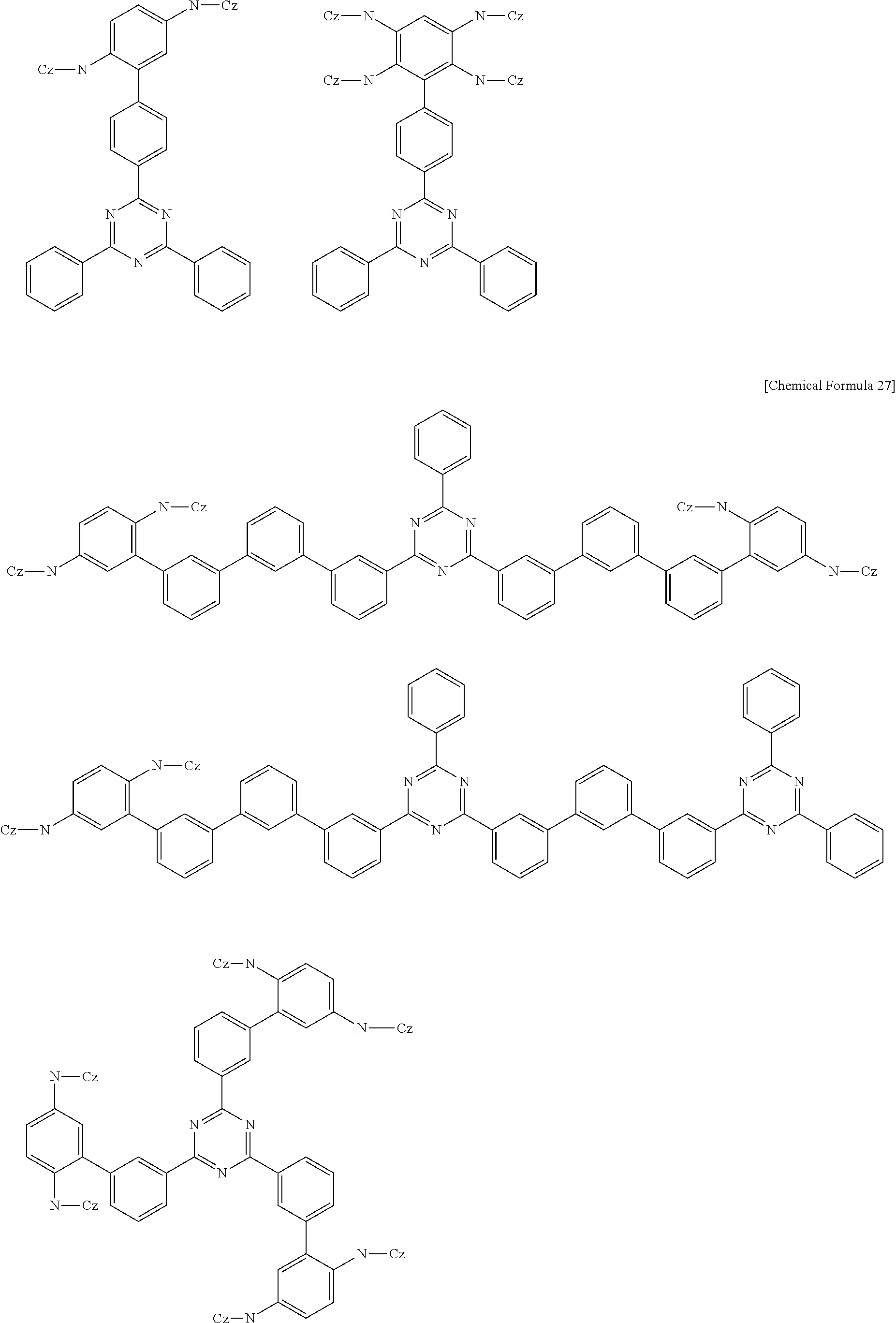


[7] Preparation Method


wherein Ar's may be the same as or different from one another and each represent an arylene group, a heteroarylene group, or an unsaturated hydrocarbon group each of which may have an arbitrary substituent such as a halogen atom, an aryl group, or a heteroaryl group.

wherein Xs each represent any one of fluorine, chlorine, bromine, and iodine; and Ars may be the same as or different from one another and each represent an arylene group, a heteroarylene group, or an unsaturated hydrocarbon group each of which may have an arbitrary substituent such as a halogen atom, an aryl group, or a heteroaryl group.
(Oxidation potential of the hole blocking material)−(Oxidation potential of the light-emitting layer material)≧0.1 V
(Reduction potential of the hole blocking material)≧(Reduction potential of the light-emitting material)
When the light-emitting
MLk−jL′j (V)


Ionization potential=(Oxidation potential (vs. SCE))+4.3 eV
Electron affinity=(Reduction potential (vs. SCE))+4.3 eV
(Oxidation potential of the hole blocking material)−(Oxidation potential of the light-emitting layer material)≧0.1 V
(Reduction potential of the hole blocking material)≧(Reduction potential of the light-emitting layer material)
(Reduction potential of the electron transporting material)≧(Reduction potential of the hole blocking material)≧(Reduction potential of the light-emitting layer material)


(Reduction potential of the electron transporting material)≧(Reduction potential of the hole blocking material)≧(Reduction potential of the light-emitting layer material)
- porphine,
- 5,10,15,20-tetraphenyl-21H,23H-porphine,
- 5,10,15,20-tetraphenyl-21H,23H-porphine cobalt(II),
- 5,10,15,20-tetraphenyl-21H,23H-porphine copper(II),
- 5,10,15,20-tetraphenyl-21H,23H-porphine zinc(II),
- 5,10,15,20-tetraphenyl-21H,23H-porphine vanadium(IV) oxide,
- 5,10,15,20-tetra(4-pyridyl)-21H,23H-porphine,
- 29H,31H-phthalocyanine,
- copper(II) phthalocyanine,
- zinc(II) phthalocyanine,
- titanium phthalocyanine oxide,
- magnesium phthalocyanine,
- lead phthalocyanine, and
- copper(II) 4,4′4″,4′″-tetraaza-29H,31H-phthalocyanine


| TABLE 1 | |
| Properties of device | |
| Component of device | Luminous | Luminance |
| Host material | Hole blocking | Current efficiency | Voltage | efficiency | holding ratio | Driving lifetime | |
| of light-emitting layer | material | (@2.5 mA/cm2) | (@2.5 mA/cm2) | (@100 cd/m2) | (@250 mA/cm2) | (@2,500 cd/m2) | |
| Referential | CBP | HB-1 | 1.00 | 1.00 | 1.00 | 1.00 | |
| |
|||||||
| Referential | CBP | — | 0.60 | 1.15 | 0.52 | 1.03 | 1.00 |
| |
|||||||
| Example 1 | EM-1 | HB-1 | 1.20 | 0.97 | 1.24 | 0.99 | 1.14 |
| Example 2 | EM-1 | — | 1.03 | 0.91 | 1.13 | 0.99 | 0.93 |
| Example 3 | EM-2 | HB-1 | 0.99 | 1.12 | 0.88 | 0.98 | 1.50 |
| Example 4 | EM-2 | — | 0.93 | 1.01 | 0.92 | 0.98 | 1.13 |
| Example 5 | EM-3 | HB-1 | 1.09 | 0.75 | 1.45 | 0.95 | |
| Example 6 | EM-3 | — | 1.13 | 0.7 | 1.61 | 0.95 | |
| Example 7 | EM-4 | HB-1 | 1.10 | 0.96 | 1.10 | 0.95 | |
| Example 8 | EM-4 | — | 1.07 | 0.91 | 1.05 | 0.96 | |
| Example 9 | EM-5 | HB-1 | 1.23 | 1.02 | 1.22 | 1.00 | |
| Example 10 | EM-5 | 1.15 | 0.89 | 1.34 | 0.96 | ||
| Example 11 | EM-6 | HB-1 | |||||
| Example 12 | EM-6 | — | 1.13 | 0.90 | 1.01 | 0.98 | |
| Com. Ex. 1 | EM-11 | HB-1 | 0.84 | 1.13 | 0.74 | 0.96 | 0.66 |
| Com. Ex. 2 | EM-11 | — | 0.85 | 1.04 | 0.81 | 0.97 | 0.66 |
Claims (13)


Applications Claiming Priority (3)
| Application Number | Priority Date | Filing Date | Title |
|---|---|---|---|
| JP2004373981 | 2004-12-24 | ||
| JP2004-373981 | 2004-12-24 | ||
| PCT/JP2005/022635 WO2006067976A1 (en) | 2004-12-24 | 2005-12-09 | Organic compound, charge-transporting material, and organic electroluminescent element |
Publications (3)
| Publication Number | Publication Date |
|---|---|
| US20080145699A1 US20080145699A1 (en) | 2008-06-19 |
| US20090191426A2 US20090191426A2 (en) | 2009-07-30 |
| US8324403B2 true US8324403B2 (en) | 2012-12-04 |
Family
ID=36601578
Family Applications (1)
| Application Number | Title | Priority Date | Filing Date |
|---|---|---|---|
| US11/722,760 Active 2029-03-03 US8324403B2 (en) | 2004-12-24 | 2005-12-09 | Organic compound, charge-transporting material, and organic electroluminescent element |
Country Status (7)
| Country | Link |
|---|---|
| US (1) | US8324403B2 (en) |
| EP (1) | EP1829871B1 (en) |
| JP (1) | JP5050344B2 (en) |
| KR (2) | KR20120082938A (en) |
| CN (1) | CN101087776B (en) |
| TW (1) | TWI380980B (en) |
| WO (1) | WO2006067976A1 (en) |
Cited By (9)
| Publication number | Priority date | Publication date | Assignee | Title |
|---|---|---|---|---|
| US20110204894A1 (en) * | 2010-02-24 | 2011-08-25 | Andreas Kamlowski | Analysis system with GPC and NMR spectroscopy coupling, in particular for the analysis of samples having polymers |
| US20150249217A1 (en) * | 2014-02-28 | 2015-09-03 | Samsung Display Co., Ltd. | Triazine-containing compound and organic electroluminescent device including the same |
| US10193077B2 (en) | 2010-04-20 | 2019-01-29 | Idemitsu Kosan Co., Ltd. | Biscarbazole derivative, material for organic electroluminescence device and organic electroluminescence device using the same |
| US10636976B2 (en) | 2016-02-26 | 2020-04-28 | Semiconductor Energy Laboratory Co., Ltd. | Organic compound, light-emitting element, light-emitting device, electronic device, and lighting device |
| US10741774B2 (en) | 2017-07-04 | 2020-08-11 | Samsung Display Co., Ltd. | Heterocyclic compound and organic electroluminescence device including the same |
| US11542252B2 (en) | 2018-12-28 | 2023-01-03 | Samsung Electronics Co., Ltd. | Heterocyclic compound, composition including the same, and organic light-emitting device including the heterocyclic compound |
| US11758808B2 (en) | 2015-03-27 | 2023-09-12 | Samsung Display Co., Ltd. | Ortho-substituted thermally activated delayed fluorescence material and organic light-emitting device comprising same |
| US11991927B2 (en) | 2020-01-28 | 2024-05-21 | Samsung Electronics Co., Ltd. | Organic light-emitting device |
| US12520720B2 (en) | 2018-08-27 | 2026-01-06 | Samsung Electronics Co., Ltd. | Heterocyclic compound and organic light-emitting device |
Families Citing this family (92)
| Publication number | Priority date | Publication date | Assignee | Title |
|---|---|---|---|---|
| US8178215B2 (en) | 2004-12-10 | 2012-05-15 | Pioneer Corporation | Organic compound containing at least two carbazolyl-substituted phenyl structures; charge-transporting material and organic el element containing the compound |
| WO2006104221A1 (en) | 2005-03-28 | 2006-10-05 | Semiconductor Energy Laboratory Co., Ltd. | Anthracene derivative, material for light emitting element, light emitting element, light emitting device, and electronic device |
| EP1887640A4 (en) * | 2005-05-24 | 2012-04-04 | Pioneer Corp | ORGANIC ELECTROLUMINESCENCE DEVICE |
| JP5168840B2 (en) * | 2005-08-04 | 2013-03-27 | 三菱化学株式会社 | Charge transport material, composition for organic electroluminescence device, and organic electroluminescence device |
| JP5167607B2 (en) * | 2005-08-23 | 2013-03-21 | 三菱化学株式会社 | Charge transport material, charge transport material composition, and organic electroluminescent device |
| JP5017858B2 (en) * | 2005-12-27 | 2012-09-05 | コニカミノルタホールディングス株式会社 | Organic electroluminescence device |
| TW200804452A (en) * | 2006-03-13 | 2008-01-16 | Sumitomo Chemical Co | Method for production of conjugated polymer |
| DE102006025777A1 (en) * | 2006-05-31 | 2007-12-06 | Merck Patent Gmbh | New materials for organic electroluminescent devices |
| JP5179805B2 (en) * | 2006-08-30 | 2013-04-10 | 株式会社半導体エネルギー研究所 | Anthracene derivative, light emitting element and light emitting device |
| CN101506163B (en) | 2006-08-30 | 2012-05-02 | 株式会社半导体能源研究所 | Method for synthesizing anthracene derivative and anthracene derivative, light emitting element, light emitting device, electronic device |
| JP5167747B2 (en) * | 2006-10-04 | 2013-03-21 | 三菱化学株式会社 | Charge transport material for low molecular weight coating type organic electroluminescent device, composition for organic electroluminescent device, thin film for organic electroluminescent device, and organic electroluminescent device |
| JP5153127B2 (en) * | 2006-11-28 | 2013-02-27 | キヤノン株式会社 | Amine compound and organic light emitting device |
| JP5504563B2 (en) * | 2006-12-27 | 2014-05-28 | 住友化学株式会社 | Composition and light-emitting device using the composition |
| US7723722B2 (en) | 2007-03-23 | 2010-05-25 | Semiconductor Energy Laboratory Co., Ltd. | Organic compound, anthracene derivative, and light-emitting element, light-emitting device, and electronic device using anthracene derivative |
| CN101657517B (en) * | 2007-04-13 | 2013-03-27 | 第一毛织株式会社 | Material for organic photoelectric device including electron transporting unit and hole transporting unit, and organic photoelectric device including the same |
| KR100957620B1 (en) * | 2007-11-01 | 2010-05-13 | 제일모직주식회사 | Material for organic photoelectric device, and organic photoelectric device using same |
| JP5487595B2 (en) * | 2007-11-15 | 2014-05-07 | 三菱化学株式会社 | Composition for organic electroluminescent device and organic electroluminescent device |
| JP5499487B2 (en) * | 2008-02-25 | 2014-05-21 | 三菱化学株式会社 | Quinoline compounds, materials for organic electroluminescent elements, compositions for organic electroluminescent elements, organic electroluminescent elements, organic EL displays, and organic EL lighting |
| WO2009119163A1 (en) | 2008-03-24 | 2009-10-01 | 新日鐵化学株式会社 | Compound for organic electroluminescent device and organic electroluminescent device using the same |
| JP5604804B2 (en) * | 2008-04-25 | 2014-10-15 | 住友化学株式会社 | Composition comprising a nitrogen-containing heterocyclic compound |
| US8049411B2 (en) | 2008-06-05 | 2011-11-01 | Idemitsu Kosan Co., Ltd. | Material for organic electroluminescence device and organic electroluminescence device using the same |
| KR101523124B1 (en) * | 2008-06-05 | 2015-05-26 | 이데미쓰 고산 가부시키가이샤 | Halogen compound, polycyclic compound, and organic electroluminescence element comprising the polycyclic compound |
| JP2010013421A (en) * | 2008-07-07 | 2010-01-21 | Chemiprokasei Kaisha Ltd | New bis(dicarbazolylphenyl) derivative, host material using the same and organic electroluminescencent device |
| JP5371312B2 (en) * | 2008-07-28 | 2013-12-18 | ケミプロ化成株式会社 | Novel dicarbazolylphenyl derivative, host material using the same, and organic electroluminescence device |
| ATE517088T1 (en) | 2008-09-19 | 2011-08-15 | Semiconductor Energy Lab | CARBAZOLE DERIVATIVE AND PRODUCTION METHOD THEREOF |
| DE102008050841B4 (en) * | 2008-10-08 | 2019-08-01 | Merck Patent Gmbh | New materials for organic electroluminescent devices |
| JP5674266B2 (en) * | 2008-10-27 | 2015-02-25 | ケミプロ化成株式会社 | Novel carbazole derivative, host material comprising the same, and organic electroluminescence device including the same |
| KR101288557B1 (en) * | 2008-12-24 | 2013-07-22 | 제일모직주식회사 | Novel compound for organic photoelectric device and organic photoelectric device including the same |
| KR101233377B1 (en) * | 2008-12-30 | 2013-02-18 | 제일모직주식회사 | Novel compound for organic photoelectricand organic photoelectric device including the same |
| JP4523992B1 (en) | 2009-07-31 | 2010-08-11 | 富士フイルム株式会社 | Organic electroluminescence device |
| JP4474493B1 (en) | 2009-07-31 | 2010-06-02 | 富士フイルム株式会社 | Organic electroluminescence device |
| JP4590020B1 (en) * | 2009-07-31 | 2010-12-01 | 富士フイルム株式会社 | Charge transport material and organic electroluminescent device |
| EP2477999B1 (en) * | 2009-09-16 | 2019-01-23 | Merck Patent GmbH | Formulations for electronic devices |
| CN102471320A (en) | 2009-10-16 | 2012-05-23 | 出光兴产株式会社 | Fluorene-containing aromatic compound, material for organic electroluminescent element, and organic electroluminescent element using same |
| US8828561B2 (en) | 2009-11-03 | 2014-09-09 | Cheil Industries, Inc. | Compound for organic photoelectric device and organic photoelectric device including the same |
| KR101506999B1 (en) | 2009-11-03 | 2015-03-31 | 제일모직 주식회사 | Compound for organic photoelectric device and organic photoelectric device including the same |
| DE102009053382A1 (en) | 2009-11-14 | 2011-05-19 | Merck Patent Gmbh | Materials for electronic devices |
| JPWO2011108707A1 (en) | 2010-03-05 | 2013-06-27 | 出光興産株式会社 | Material for organic electroluminescence device and organic electroluminescence device using the same |
| CN105949177B (en) | 2010-05-03 | 2019-02-01 | 默克专利有限公司 | Preparation and electronic device |
| CN102869672B (en) | 2010-05-03 | 2016-05-11 | 默克专利有限公司 | Preparation and electronic device |
| JP5783173B2 (en) | 2010-06-02 | 2015-09-24 | Jnc株式会社 | Carbazole compounds having substituents containing electron-accepting nitrogen-containing heteroaryl and organic electroluminescent devices |
| JP6007467B2 (en) * | 2010-07-27 | 2016-10-12 | コニカミノルタ株式会社 | Organic electroluminescence element material, organic electroluminescence element, |
| JP5664128B2 (en) * | 2010-10-29 | 2015-02-04 | 三菱化学株式会社 | Pyrimidine compound, material for organic electroluminescence device, composition for organic electroluminescence device, organic electroluminescence device, lighting device and display device |
| DE112011103904B4 (en) | 2010-11-24 | 2022-12-15 | Merck Patent Gmbh | Materials for organic electroluminescent devices |
| KR101531612B1 (en) | 2010-12-02 | 2015-06-25 | 제일모직 주식회사 | Compound for organic photoelectric device and organic photoelectric device including the same |
| EP2662368A4 (en) | 2010-12-20 | 2014-06-25 | Idemitsu Kosan Co | AROMATIC HETEROCYCLE DERIVATIVE AND ORGANIC ELECTROLUMINESCENT ELEMENT USING THE SAME |
| JP2014507401A (en) * | 2010-12-20 | 2014-03-27 | イー・アイ・デュポン・ドウ・ヌムール・アンド・カンパニー | Triazine derivatives for electronics applications |
| JP5926286B2 (en) * | 2010-12-21 | 2016-05-25 | イー・アイ・デュポン・ドウ・ヌムール・アンド・カンパニーE.I.Du Pont De Nemours And Company | Electronic devices containing pyrimidine compounds |
| EP2676305A4 (en) * | 2011-02-14 | 2015-11-11 | Du Pont | ELECTROACTIVE COMPOSITION |
| US10177312B2 (en) | 2011-05-05 | 2019-01-08 | Merck Patent Gmbh | Compounds for electronic devices |
| WO2013077362A1 (en) | 2011-11-22 | 2013-05-30 | 出光興産株式会社 | Aromatic heterocyclic derivative, material for organic electroluminescent element, and organic electroluminescent element |
| JP6060095B2 (en) * | 2012-02-03 | 2017-01-11 | 出光興産株式会社 | Carbazole compound, material for organic electroluminescence device, and organic electroluminescence device |
| JP6066132B2 (en) | 2012-07-13 | 2017-01-25 | エルジー・ケム・リミテッド | Heterocyclic compounds and organic electronic devices containing the same |
| JP5819534B2 (en) | 2012-09-11 | 2015-11-24 | Jnc株式会社 | Organic electroluminescent element material, organic electroluminescent element, display device, and illumination device |
| WO2015072520A1 (en) | 2013-11-13 | 2015-05-21 | 出光興産株式会社 | Compound, material for organic electroluminescent element, organic electroluminescent element, and electronic device |
| CN104370887B (en) * | 2013-12-26 | 2016-08-24 | 北京阿格蕾雅科技发展有限公司 | Synthetic method of 2,6-bis[3-(N-carbazolyl)phenyl]pyridine compounds |
| KR101829745B1 (en) | 2014-01-24 | 2018-02-19 | 삼성에스디아이 주식회사 | Organic compound and composition and organic optoelectric device and display device |
| KR101773363B1 (en) | 2014-04-09 | 2017-08-31 | 제일모직 주식회사 | Organic compound and composition and organic optoelectric device and display device |
| EP3663289A1 (en) * | 2014-06-11 | 2020-06-10 | Hodogaya Chemical Co., Ltd. | Pyrimidine derivatives and an organic electroluminescent devices |
| CN105254555B (en) * | 2014-07-09 | 2020-12-29 | 三星电子株式会社 | Condensed ring compound and organic light-emitting device including the same |
| KR101887213B1 (en) * | 2014-08-12 | 2018-08-09 | 삼성에스디아이 주식회사 | Compound, organic optoelectric device and display device |
| US10784446B2 (en) | 2014-11-28 | 2020-09-22 | Idemitsu Kosan Co., Ltd. | Compound, organic electroluminescence element material, organic electroluminescence element and electronic device |
| KR102249062B1 (en) * | 2014-11-28 | 2021-05-10 | 덕산네오룩스 주식회사 | Compound for organic electronic element, organic electronic element using the same, and an electronic device thereof |
| JP6694830B2 (en) * | 2015-02-13 | 2020-05-20 | 出光興産株式会社 | Compound, composition, organic electroluminescence device, and electronic device |
| EP3065190A1 (en) | 2015-03-02 | 2016-09-07 | Ecole Polytechnique Fédérale de Lausanne (EPFL) | Small molecule hole transporting material for optoelectronic and photoelectrochemical devices |
| KR20170131398A (en) * | 2015-03-27 | 2017-11-29 | 이데미쓰 고산 가부시키가이샤 | Organic electroluminescence devices, electronic devices, and compounds |
| CN107592860B (en) * | 2015-04-24 | 2020-11-03 | 三星Sdi株式会社 | Organic compounds, compositions and organic photodiodes |
| KR102146446B1 (en) * | 2015-05-08 | 2020-08-20 | 코니카 미놀타 가부시키가이샤 | π conjugated compounds, organic electroluminescent device materials, luminescent materials, luminescent thin films, organic electroluminescent devices, display devices and lighting devices |
| JP6056909B2 (en) * | 2015-06-11 | 2017-01-11 | コニカミノルタ株式会社 | Organic electroluminescence device |
| KR101962758B1 (en) | 2015-06-17 | 2019-03-27 | 삼성에스디아이 주식회사 | Organic compound for optoelectric device and organic optoelectric device and display device |
| JP6969081B2 (en) * | 2015-09-10 | 2021-11-24 | 東ソー株式会社 | Cyclic azine compounds, their production methods, production intermediates, and uses |
| TWI705061B (en) * | 2016-08-24 | 2020-09-21 | 德商賽諾拉公司 | Organic molecules, especially for use in organic optoelectronic devices |
| JP6902859B2 (en) * | 2016-12-08 | 2021-07-14 | 東ソー株式会社 | Soluble azine compound and its manufacturing method, and organic electroluminescent device using it |
| DE102017102363B4 (en) * | 2017-02-07 | 2020-11-05 | Cynora Gmbh | Organic molecules, in particular for use in organic optoelectronic devices |
| KR102559835B1 (en) | 2017-02-07 | 2023-07-27 | 삼성디스플레이 주식회사 | Organic Molecules, In particular Organic Molecules for Use in Organic Optoelectronic Devices |
| US11393984B2 (en) | 2017-04-13 | 2022-07-19 | Cynora Gmbh | Organic molecules for use in organic optoelectronic devices |
| EP3418278B1 (en) * | 2017-06-23 | 2020-10-21 | Cynora Gmbh | Organic molecules, in particular for use in optoelectronic devices |
| WO2019053049A1 (en) * | 2017-09-18 | 2019-03-21 | Cynora Gmbh | Organic molecules, in particular for use in optoelectronic devices |
| WO2019073075A1 (en) * | 2017-10-13 | 2019-04-18 | Cynora Gmbh | Organic molecules for use in optoelectronic devices |
| EP3470411B1 (en) | 2017-10-16 | 2019-10-16 | Cynora Gmbh | Organic molecules, in particular for use in optoelectronic devices |
| EP3697782B1 (en) * | 2017-10-19 | 2021-09-01 | cynora GmbH | Organic molecules for use in optoelectronic devices |
| US11706977B2 (en) | 2018-01-11 | 2023-07-18 | Samsung Electronics Co., Ltd. | Heterocyclic compound, composition including the same, and organic light-emitting device including the heterocyclic compound |
| EP3575377B1 (en) * | 2018-05-31 | 2021-03-17 | Cynora Gmbh | Organic molecules for optoelectronic devices |
| CN108682702A (en) * | 2018-06-06 | 2018-10-19 | 北京大学 | A kind of photoelectric device composite hole transporting layer material and preparation method thereof |
| CN112566908A (en) * | 2018-08-13 | 2021-03-26 | 辛诺拉有限公司 | Organic molecules for optoelectronic devices |
| WO2020111602A1 (en) | 2018-11-27 | 2020-06-04 | 주식회사 엘지화학 | Novel compound and organic light-emitting element including same |
| US12022730B2 (en) | 2018-11-27 | 2024-06-25 | Lg Chem, Ltd. | Compound and organic light emitting device comprising the same |
| KR102331904B1 (en) * | 2018-11-27 | 2021-11-26 | 주식회사 엘지화학 | Novel compound and organic light emitting device comprising the same |
| KR102664397B1 (en) * | 2019-02-26 | 2024-05-08 | 삼성전자주식회사 | Heterocyclic compound and organic light emitting device including the same |
| KR102753926B1 (en) * | 2019-03-11 | 2025-01-15 | 삼성디스플레이 주식회사 | Heterocyclic compound and organic light emitting device including the same |
| CN110649165B (en) * | 2019-04-04 | 2024-06-04 | 中茂光伏科技集团有限公司 | Perovskite battery taking tetraphenyl biphenyl diamine derivative as hole transport material |
| CN111285759B (en) * | 2020-02-19 | 2022-08-12 | 贵州省中国科学院天然产物化学重点实验室(贵州医科大学天然产物化学重点实验室) | A kind of synthetic method of chalcone derivatives |
Citations (29)
| Publication number | Priority date | Publication date | Assignee | Title |
|---|---|---|---|---|
| EP0517542A1 (en) | 1991-06-05 | 1992-12-09 | Sumitomo Chemical Company, Limited | Organic electroluminescence devices |
| JPH061972A (en) | 1991-06-05 | 1994-01-11 | Sumitomo Chem Co Ltd | Organic electroluminescent device |
| JP2000169448A (en) | 1998-12-07 | 2000-06-20 | Minolta Co Ltd | New amino compound and its production, and use |
| JP2000186066A (en) | 1998-12-22 | 2000-07-04 | Minolta Co Ltd | New amino compound, its production and use thereof |
| WO2001072927A1 (en) | 2000-03-27 | 2001-10-04 | Idemitsu Kosan Co., Ltd. | Organic electroluminescence device |
| JP2002008860A (en) | 2000-04-18 | 2002-01-11 | Mitsubishi Chemicals Corp | Organic electroluminescent device |
| JP2003022893A (en) | 2001-07-06 | 2003-01-24 | Fuji Photo Film Co Ltd | Luminescent element |
| WO2003078541A1 (en) | 2002-03-15 | 2003-09-25 | Idemitsu Kosan Co., Ltd. | Material for organic electroluminescent devices and organic electroluminescent devices made by using the same |
| TW200304937A (en) | 2002-03-22 | 2003-10-16 | Idemitsu Kosan Co | Material for organic electroluminescent devices and organic electroluminescent devices made by using the same |
| US20030205696A1 (en) | 2002-04-25 | 2003-11-06 | Canon Kabushiki Kaisha | Carbazole-based materials for guest-host electroluminescent systems |
| WO2004034751A1 (en) | 2002-10-09 | 2004-04-22 | Idemitsu Kosan Co., Ltd. | Organic electroluminescent device |
| JP2004171808A (en) | 2002-11-18 | 2004-06-17 | Konica Minolta Holdings Inc | Organic electroluminescence element and display device |
| US20040137263A1 (en) * | 2001-02-20 | 2004-07-15 | Burn Paul Leslie | Metal-containing dendrimers |
| JP2004217557A (en) | 2003-01-14 | 2004-08-05 | Mitsubishi Chemicals Corp | Carbazole-based compound, charge transport material, organic electroluminescent device material, and organic electroluminescent device |
| WO2004066685A1 (en) | 2003-01-24 | 2004-08-05 | Idemitsu Kosan Co., Ltd. | Organic electroluminescence device |
| US20040212042A1 (en) * | 2003-02-13 | 2004-10-28 | Toshiya Sagisaka | Aryl amine polymer, thin film transistor using the aryl amine polymer, and method of manufacturing the thin film transistor |
| JP2004311404A (en) | 2003-03-26 | 2004-11-04 | Konica Minolta Holdings Inc | Organic electroluminescence element, lighting device and display device |
| US20040247933A1 (en) | 2003-06-03 | 2004-12-09 | Canon Kabushiki Kaisha | Bipolar asymmetric carbazole-based host materials for electrophosphorescent guest-host OLED systems |
| WO2004113468A1 (en) | 2003-06-26 | 2004-12-29 | Covion Organic Semiconductors Gmbh | Novel materials for electroluminescence |
| WO2005022962A1 (en) * | 2003-07-31 | 2005-03-10 | Mitsubishi Chemical Corporation | Compound, charge transport material and organic electroluminescent device |
| WO2005057987A1 (en) | 2003-12-15 | 2005-06-23 | Idemitsu Kosan Co., Ltd. | Material for organic electroluminescent device and organic electroluminescent device using same |
| WO2005076669A1 (en) | 2004-02-09 | 2005-08-18 | Idemitsu Kosan Co., Ltd. | Organic electroluminescent device |
| WO2005079118A1 (en) | 2004-02-13 | 2005-08-25 | Idemitsu Kosan Co., Ltd. | Organic electroluminescent device |
| WO2005084083A1 (en) | 2004-03-02 | 2005-09-09 | Idemitsu Kosan Co., Ltd. | Organic electroluminescent device |
| WO2005085387A1 (en) | 2004-03-08 | 2005-09-15 | Idemitsu Kosan Co., Ltd. | Material for organic electroluminescence device and organic electroluminescence device utilizing the same |
| JP2005268199A (en) | 2003-07-31 | 2005-09-29 | Mitsubishi Chemicals Corp | Compound, charge transport material and organic electroluminescence device |
| EP1857521A1 (en) | 2005-02-21 | 2007-11-21 | Mitsubishi Chemical Corporation | Organic electric field light emitting element and production therefor |
| EP1885008A1 (en) | 2005-05-17 | 2008-02-06 | Mitsubishi Chemical Corporation | Monoamine compound, charge-transporting material, and organic electroluminescent device |
| EP1887640A1 (en) | 2005-05-24 | 2008-02-13 | Pioneer Corporation | Organic electroluminescent device |
-
2005
- 2005-12-09 CN CN200580044718XA patent/CN101087776B/en not_active Expired - Fee Related
- 2005-12-09 EP EP05814748.9A patent/EP1829871B1/en not_active Ceased
- 2005-12-09 KR KR1020127014632A patent/KR20120082938A/en not_active Withdrawn
- 2005-12-09 KR KR1020077014364A patent/KR101420608B1/en not_active Expired - Lifetime
- 2005-12-09 WO PCT/JP2005/022635 patent/WO2006067976A1/en not_active Ceased
- 2005-12-09 JP JP2005355790A patent/JP5050344B2/en not_active Expired - Lifetime
- 2005-12-09 US US11/722,760 patent/US8324403B2/en active Active
- 2005-12-21 TW TW094145599A patent/TWI380980B/en not_active IP Right Cessation
Patent Citations (50)
| Publication number | Priority date | Publication date | Assignee | Title |
|---|---|---|---|---|
| EP0517542A1 (en) | 1991-06-05 | 1992-12-09 | Sumitomo Chemical Company, Limited | Organic electroluminescence devices |
| JPH061972A (en) | 1991-06-05 | 1994-01-11 | Sumitomo Chem Co Ltd | Organic electroluminescent device |
| JP2000169448A (en) | 1998-12-07 | 2000-06-20 | Minolta Co Ltd | New amino compound and its production, and use |
| JP2000186066A (en) | 1998-12-22 | 2000-07-04 | Minolta Co Ltd | New amino compound, its production and use thereof |
| US6660410B2 (en) | 2000-03-27 | 2003-12-09 | Idemitsu Kosan Co., Ltd. | Organic electroluminescence element |
| EP1205527A1 (en) | 2000-03-27 | 2002-05-15 | Idemitsu Kosan Co., Ltd. | Organic electroluminescence device |
| WO2001072927A1 (en) | 2000-03-27 | 2001-10-04 | Idemitsu Kosan Co., Ltd. | Organic electroluminescence device |
| JP2002008860A (en) | 2000-04-18 | 2002-01-11 | Mitsubishi Chemicals Corp | Organic electroluminescent device |
| US20040137263A1 (en) * | 2001-02-20 | 2004-07-15 | Burn Paul Leslie | Metal-containing dendrimers |
| JP2003022893A (en) | 2001-07-06 | 2003-01-24 | Fuji Photo Film Co Ltd | Luminescent element |
| WO2003078541A1 (en) | 2002-03-15 | 2003-09-25 | Idemitsu Kosan Co., Ltd. | Material for organic electroluminescent devices and organic electroluminescent devices made by using the same |
| EP1486550A1 (en) | 2002-03-15 | 2004-12-15 | Idemitsu Kosan Co., Ltd. | Material for organic electroluminescent devices and organic electroluminescent devices made by using the same |
| US20050127823A1 (en) | 2002-03-15 | 2005-06-16 | Idemitsu Kosan Co., Ltd. | Material for organic electroluminescent devices and organic electroluminescent devices made by using the same |
| TW200304937A (en) | 2002-03-22 | 2003-10-16 | Idemitsu Kosan Co | Material for organic electroluminescent devices and organic electroluminescent devices made by using the same |
| US20050249976A1 (en) | 2002-03-22 | 2005-11-10 | Idemitsu Kosan Co., Ltd. | Material for organic electroluminescence devices and organic electroluminescence device using the material |
| US20040086745A1 (en) * | 2002-03-22 | 2004-05-06 | Idemitsu Kosan Co., Ltd. | Material for organic electroluminescence devices and organic electroluminescence device using the material |
| EP1489155A1 (en) | 2002-03-22 | 2004-12-22 | Idemitsu Kosan Co., Ltd. | Material for organic electroluminescent devices and organic electroluminescent devices made by using the same |
| JP2003317966A (en) | 2002-04-25 | 2003-11-07 | Canon Inc | Carbazole-based materials for guest-host electroluminescence systems |
| US20030205696A1 (en) | 2002-04-25 | 2003-11-06 | Canon Kabushiki Kaisha | Carbazole-based materials for guest-host electroluminescent systems |
| EP1551206A1 (en) | 2002-10-09 | 2005-07-06 | Idemitsu Kosan Co., Ltd. | Organic electroluminescent device |
| US20060257684A1 (en) | 2002-10-09 | 2006-11-16 | Idemitsu Kosan Co., Ltd. | Organic electroluminescent device |
| WO2004034751A1 (en) | 2002-10-09 | 2004-04-22 | Idemitsu Kosan Co., Ltd. | Organic electroluminescent device |
| JP2004171808A (en) | 2002-11-18 | 2004-06-17 | Konica Minolta Holdings Inc | Organic electroluminescence element and display device |
| JP2004217557A (en) | 2003-01-14 | 2004-08-05 | Mitsubishi Chemicals Corp | Carbazole-based compound, charge transport material, organic electroluminescent device material, and organic electroluminescent device |
| WO2004066685A1 (en) | 2003-01-24 | 2004-08-05 | Idemitsu Kosan Co., Ltd. | Organic electroluminescence device |
| TW200417279A (en) | 2003-01-24 | 2004-09-01 | Idemitsu Kosan Co | Organic electroluminescence device |
| US20060180806A1 (en) * | 2003-01-24 | 2006-08-17 | Takashi Arakane | Organic electroluminescence device |
| US20040212042A1 (en) * | 2003-02-13 | 2004-10-28 | Toshiya Sagisaka | Aryl amine polymer, thin film transistor using the aryl amine polymer, and method of manufacturing the thin film transistor |
| JP2004311404A (en) | 2003-03-26 | 2004-11-04 | Konica Minolta Holdings Inc | Organic electroluminescence element, lighting device and display device |
| US20040247933A1 (en) | 2003-06-03 | 2004-12-09 | Canon Kabushiki Kaisha | Bipolar asymmetric carbazole-based host materials for electrophosphorescent guest-host OLED systems |
| WO2004113468A1 (en) | 2003-06-26 | 2004-12-29 | Covion Organic Semiconductors Gmbh | Novel materials for electroluminescence |
| WO2005022962A1 (en) * | 2003-07-31 | 2005-03-10 | Mitsubishi Chemical Corporation | Compound, charge transport material and organic electroluminescent device |
| JP2005268199A (en) | 2003-07-31 | 2005-09-29 | Mitsubishi Chemicals Corp | Compound, charge transport material and organic electroluminescence device |
| EP1672961A1 (en) | 2003-07-31 | 2006-06-21 | Mitsubishi Chemical Corporation | Compound, charge transport material and organic electroluminescent device |
| US20070104976A1 (en) | 2003-12-15 | 2007-05-10 | Idemitsu Kosan Co., Ltd. | Material for organic electroluminescent device and organic electroluminescent device using same |
| TW200524464A (en) | 2003-12-15 | 2005-07-16 | Idemitsu Kosan Co | Material for organic electroluminescent device and organic electroluminescent device using same |
| WO2005057987A1 (en) | 2003-12-15 | 2005-06-23 | Idemitsu Kosan Co., Ltd. | Material for organic electroluminescent device and organic electroluminescent device using same |
| TW200533239A (en) | 2004-02-09 | 2005-10-01 | Idemitsu Kosan Co | Organic electroluminescent device |
| WO2005076669A1 (en) | 2004-02-09 | 2005-08-18 | Idemitsu Kosan Co., Ltd. | Organic electroluminescent device |
| EP1718121A1 (en) | 2004-02-09 | 2006-11-02 | Idemitsu Kosan Co., Ltd. | Organic electroluminescent device |
| TW200541401A (en) | 2004-02-13 | 2005-12-16 | Idemitsu Kosan Co | Organic electroluminescent device |
| WO2005079118A1 (en) | 2004-02-13 | 2005-08-25 | Idemitsu Kosan Co., Ltd. | Organic electroluminescent device |
| US20070159083A1 (en) | 2004-02-13 | 2007-07-12 | Idemitsu Kosan Co., Ltd. | Organic electroluminescent device |
| WO2005084083A1 (en) | 2004-03-02 | 2005-09-09 | Idemitsu Kosan Co., Ltd. | Organic electroluminescent device |
| US20070172698A1 (en) | 2004-03-02 | 2007-07-26 | Idemitsu Kosan Co., Ltd. | Organic electroluminescent device |
| WO2005085387A1 (en) | 2004-03-08 | 2005-09-15 | Idemitsu Kosan Co., Ltd. | Material for organic electroluminescence device and organic electroluminescence device utilizing the same |
| EP1724323A1 (en) | 2004-03-08 | 2006-11-22 | Idemitsu Kosan Co., Ltd. | Material for organic electroluminescence device and organic electroluminescence device utilizing the same |
| EP1857521A1 (en) | 2005-02-21 | 2007-11-21 | Mitsubishi Chemical Corporation | Organic electric field light emitting element and production therefor |
| EP1885008A1 (en) | 2005-05-17 | 2008-02-06 | Mitsubishi Chemical Corporation | Monoamine compound, charge-transporting material, and organic electroluminescent device |
| EP1887640A1 (en) | 2005-05-24 | 2008-02-13 | Pioneer Corporation | Organic electroluminescent device |
Non-Patent Citations (8)
| Title |
|---|
| Japanese Office Action issued Jan. 31, 2012 in patent application No. 2005-355790. |
| M. A. Baldo, et al., "Very High-Efficiency Green Organic Light-Emitting Devices Based on Electrophosphorescence", Applied Physics Letters, vol. 75, No. 1, pp. 4-6, 1999. |
| Machine English translation JP 2000-169448 A. May 20, 2011. * |
| Office Action issued Apr. 16, 2012, in Taiwanese Patent Application No. 094145599 filed Dec. 21, 2005 (with English translation). |
| Office Action issued Jun. 11, 2012, in European Patent Application No. 05814748.9 filed Dec. 9, 2005. |
| Office Action issued Jun. 9, 2011, in China patent Application No. 200580044718.X (with English translation). |
| Third Party's Opinion issued Feb. 8, 2012, in European Patent Application No. 05814748.9. |
| Zhang, Q.; Chen, J.; Cheng, Y.; Wang, L.; Ma, D.; Jing, X.; Wang, F. J. Mater. Chem., 2004, 14, 895-900. * |
Cited By (12)
| Publication number | Priority date | Publication date | Assignee | Title |
|---|---|---|---|---|
| US20110204894A1 (en) * | 2010-02-24 | 2011-08-25 | Andreas Kamlowski | Analysis system with GPC and NMR spectroscopy coupling, in particular for the analysis of samples having polymers |
| US8624599B2 (en) * | 2010-02-24 | 2014-01-07 | Bruker Biospin Gmbh | Analysis system with GPC and NMR spectroscopy coupling, in particular for the analysis of samples having polymers |
| US10193077B2 (en) | 2010-04-20 | 2019-01-29 | Idemitsu Kosan Co., Ltd. | Biscarbazole derivative, material for organic electroluminescence device and organic electroluminescence device using the same |
| US20150249217A1 (en) * | 2014-02-28 | 2015-09-03 | Samsung Display Co., Ltd. | Triazine-containing compound and organic electroluminescent device including the same |
| US11758808B2 (en) | 2015-03-27 | 2023-09-12 | Samsung Display Co., Ltd. | Ortho-substituted thermally activated delayed fluorescence material and organic light-emitting device comprising same |
| US10636976B2 (en) | 2016-02-26 | 2020-04-28 | Semiconductor Energy Laboratory Co., Ltd. | Organic compound, light-emitting element, light-emitting device, electronic device, and lighting device |
| US10741774B2 (en) | 2017-07-04 | 2020-08-11 | Samsung Display Co., Ltd. | Heterocyclic compound and organic electroluminescence device including the same |
| US11165026B2 (en) | 2017-07-04 | 2021-11-02 | Samsung Display Co., Ltd. | Heterocyclic compound and organic electroluminescence device including the same |
| US12520720B2 (en) | 2018-08-27 | 2026-01-06 | Samsung Electronics Co., Ltd. | Heterocyclic compound and organic light-emitting device |
| US11542252B2 (en) | 2018-12-28 | 2023-01-03 | Samsung Electronics Co., Ltd. | Heterocyclic compound, composition including the same, and organic light-emitting device including the heterocyclic compound |
| US12060344B2 (en) | 2018-12-28 | 2024-08-13 | Samsung Electronics Co., Ltd. | Heterocyclic compound, composition including the same, and organic light-emitting device including the heterocyclic compound |
| US11991927B2 (en) | 2020-01-28 | 2024-05-21 | Samsung Electronics Co., Ltd. | Organic light-emitting device |
Also Published As
| Publication number | Publication date |
|---|---|
| KR20120082938A (en) | 2012-07-24 |
| EP1829871A4 (en) | 2009-12-16 |
| TWI380980B (en) | 2013-01-01 |
| WO2006067976A1 (en) | 2006-06-29 |
| KR20070090952A (en) | 2007-09-06 |
| CN101087776B (en) | 2012-07-04 |
| TW200631941A (en) | 2006-09-16 |
| EP1829871B1 (en) | 2015-08-12 |
| JP5050344B2 (en) | 2012-10-17 |
| US20080145699A1 (en) | 2008-06-19 |
| US20090191426A2 (en) | 2009-07-30 |
| EP1829871A1 (en) | 2007-09-05 |
| JP2006199679A (en) | 2006-08-03 |
| CN101087776A (en) | 2007-12-12 |
| KR101420608B1 (en) | 2014-07-18 |
Similar Documents
| Publication | Publication Date | Title |
|---|---|---|
| US8324403B2 (en) | Organic compound, charge-transporting material, and organic electroluminescent element | |
| US8178215B2 (en) | Organic compound containing at least two carbazolyl-substituted phenyl structures; charge-transporting material and organic el element containing the compound | |
| US8168307B2 (en) | Organic compound, charge transport material and organic electroluminescent device | |
| US8877355B2 (en) | Monoamine compound, charge-transporting material, and organic electroluminescent device | |
| US7777043B2 (en) | Compound, charge transporting material and organic electroluminescent element | |
| JP5082230B2 (en) | Organic compounds, charge transport materials, and organic electroluminescent devices | |
| KR101395615B1 (en) | Organic compound, charge-transporting material, composition for charge-transporting material and organic electroluminescent device | |
| US20200377489A1 (en) | Compound for organic optoelectronic device, composition for organic optoelectronic device, organic optoelectronic device, and display device | |
| US20140316136A1 (en) | Novel organic electroluminescence compounds and organic electroluminescence device comprising same | |
| US20170179406A1 (en) | An organic electroluminescent compound and an organic electroluminescent device comprising the same | |
| US9698355B2 (en) | Organic electroluminescent compounds and organic electroluminescent device comprising the same | |
| JP2007169268A (en) | Organic compound, charge transport material, charge transport material composition, and organic electroluminescent device | |
| US20170305854A1 (en) | Novel organic electroluminescent compounds and an organic electroluminescent device comprising the same |
Legal Events
| Date | Code | Title | Description |
|---|---|---|---|
| AS | Assignment |
Owner name: PIONEER CORPORATION, JAPAN Free format text: ASSIGNMENT OF ASSIGNORS INTEREST;ASSIGNORS:YABE, MASAYOSHI;SATO, HIDEKI;REEL/FRAME:019513/0582;SIGNING DATES FROM 20070329 TO 20070330 Owner name: MITSUBISHI CHEMICAL CORPORATION, JAPAN Free format text: ASSIGNMENT OF ASSIGNORS INTEREST;ASSIGNORS:YABE, MASAYOSHI;SATO, HIDEKI;REEL/FRAME:019513/0582;SIGNING DATES FROM 20070329 TO 20070330 Owner name: PIONEER CORPORATION, JAPAN Free format text: ASSIGNMENT OF ASSIGNORS INTEREST;ASSIGNORS:YABE, MASAYOSHI;SATO, HIDEKI;SIGNING DATES FROM 20070329 TO 20070330;REEL/FRAME:019513/0582 Owner name: MITSUBISHI CHEMICAL CORPORATION, JAPAN Free format text: ASSIGNMENT OF ASSIGNORS INTEREST;ASSIGNORS:YABE, MASAYOSHI;SATO, HIDEKI;SIGNING DATES FROM 20070329 TO 20070330;REEL/FRAME:019513/0582 |
|
| STCF | Information on status: patent grant |
Free format text: PATENTED CASE |
|
| CC | Certificate of correction | ||
| FPAY | Fee payment |
Year of fee payment: 4 |
|
| AS | Assignment |
Owner name: MITSUBISHI RAYON CO., LTD., JAPAN Free format text: MERGER;ASSIGNOR:MITSUBISHI CHEMICAL CORPORATION;REEL/FRAME:043750/0207 Effective date: 20170401 |
|
| AS | Assignment |
Owner name: MITSUBISHI CHEMICAL CORPORATION, JAPAN Free format text: CHANGE OF NAME;ASSIGNOR:MITSUBISHI RAYON CO., LTD.;REEL/FRAME:043750/0834 Effective date: 20170401 |
|
| MAFP | Maintenance fee payment |
Free format text: PAYMENT OF MAINTENANCE FEE, 8TH YEAR, LARGE ENTITY (ORIGINAL EVENT CODE: M1552); ENTITY STATUS OF PATENT OWNER: LARGE ENTITY Year of fee payment: 8 |
|
| MAFP | Maintenance fee payment |
Free format text: PAYMENT OF MAINTENANCE FEE, 12TH YEAR, LARGE ENTITY (ORIGINAL EVENT CODE: M1553); ENTITY STATUS OF PATENT OWNER: LARGE ENTITY Year of fee payment: 12 |