WO2005076669A1 - Organic electroluminescent device - Google Patents
Organic electroluminescent device Download PDFInfo
- Publication number
- WO2005076669A1 WO2005076669A1 PCT/JP2005/001799 JP2005001799W WO2005076669A1 WO 2005076669 A1 WO2005076669 A1 WO 2005076669A1 JP 2005001799 W JP2005001799 W JP 2005001799W WO 2005076669 A1 WO2005076669 A1 WO 2005076669A1
- Authority
- WO
- WIPO (PCT)
- Prior art keywords
- group
- layer
- electron transporting
- light emitting
- organic
- Prior art date
Links
Classifications
-
- H—ELECTRICITY
- H10—SEMICONDUCTOR DEVICES; ELECTRIC SOLID-STATE DEVICES NOT OTHERWISE PROVIDED FOR
- H10K—ORGANIC ELECTRIC SOLID-STATE DEVICES
- H10K85/00—Organic materials used in the body or electrodes of devices covered by this subclass
- H10K85/60—Organic compounds having low molecular weight
- H10K85/649—Aromatic compounds comprising a hetero atom
- H10K85/654—Aromatic compounds comprising a hetero atom comprising only nitrogen as heteroatom
-
- C—CHEMISTRY; METALLURGY
- C09—DYES; PAINTS; POLISHES; NATURAL RESINS; ADHESIVES; COMPOSITIONS NOT OTHERWISE PROVIDED FOR; APPLICATIONS OF MATERIALS NOT OTHERWISE PROVIDED FOR
- C09K—MATERIALS FOR MISCELLANEOUS APPLICATIONS, NOT PROVIDED FOR ELSEWHERE
- C09K11/00—Luminescent, e.g. electroluminescent, chemiluminescent materials
- C09K11/06—Luminescent, e.g. electroluminescent, chemiluminescent materials containing organic luminescent materials
-
- H—ELECTRICITY
- H05—ELECTRIC TECHNIQUES NOT OTHERWISE PROVIDED FOR
- H05B—ELECTRIC HEATING; ELECTRIC LIGHT SOURCES NOT OTHERWISE PROVIDED FOR; CIRCUIT ARRANGEMENTS FOR ELECTRIC LIGHT SOURCES, IN GENERAL
- H05B33/00—Electroluminescent light sources
- H05B33/12—Light sources with substantially two-dimensional radiating surfaces
- H05B33/14—Light sources with substantially two-dimensional radiating surfaces characterised by the chemical or physical composition or the arrangement of the electroluminescent material, or by the simultaneous addition of the electroluminescent material in or onto the light source
-
- H—ELECTRICITY
- H05—ELECTRIC TECHNIQUES NOT OTHERWISE PROVIDED FOR
- H05B—ELECTRIC HEATING; ELECTRIC LIGHT SOURCES NOT OTHERWISE PROVIDED FOR; CIRCUIT ARRANGEMENTS FOR ELECTRIC LIGHT SOURCES, IN GENERAL
- H05B33/00—Electroluminescent light sources
- H05B33/12—Light sources with substantially two-dimensional radiating surfaces
- H05B33/22—Light sources with substantially two-dimensional radiating surfaces characterised by the chemical or physical composition or the arrangement of auxiliary dielectric or reflective layers
-
- H—ELECTRICITY
- H10—SEMICONDUCTOR DEVICES; ELECTRIC SOLID-STATE DEVICES NOT OTHERWISE PROVIDED FOR
- H10K—ORGANIC ELECTRIC SOLID-STATE DEVICES
- H10K50/00—Organic light-emitting devices
- H10K50/10—OLEDs or polymer light-emitting diodes [PLED]
- H10K50/11—OLEDs or polymer light-emitting diodes [PLED] characterised by the electroluminescent [EL] layers
-
- H—ELECTRICITY
- H10—SEMICONDUCTOR DEVICES; ELECTRIC SOLID-STATE DEVICES NOT OTHERWISE PROVIDED FOR
- H10K—ORGANIC ELECTRIC SOLID-STATE DEVICES
- H10K50/00—Organic light-emitting devices
- H10K50/10—OLEDs or polymer light-emitting diodes [PLED]
- H10K50/14—Carrier transporting layers
-
- H—ELECTRICITY
- H10—SEMICONDUCTOR DEVICES; ELECTRIC SOLID-STATE DEVICES NOT OTHERWISE PROVIDED FOR
- H10K—ORGANIC ELECTRIC SOLID-STATE DEVICES
- H10K85/00—Organic materials used in the body or electrodes of devices covered by this subclass
- H10K85/60—Organic compounds having low molecular weight
- H10K85/649—Aromatic compounds comprising a hetero atom
- H10K85/657—Polycyclic condensed heteroaromatic hydrocarbons
- H10K85/6572—Polycyclic condensed heteroaromatic hydrocarbons comprising only nitrogen in the heteroaromatic polycondensed ring system, e.g. phenanthroline or carbazole
-
- H—ELECTRICITY
- H10—SEMICONDUCTOR DEVICES; ELECTRIC SOLID-STATE DEVICES NOT OTHERWISE PROVIDED FOR
- H10K—ORGANIC ELECTRIC SOLID-STATE DEVICES
- H10K2101/00—Properties of the organic materials covered by group H10K85/00
- H10K2101/10—Triplet emission
-
- H—ELECTRICITY
- H10—SEMICONDUCTOR DEVICES; ELECTRIC SOLID-STATE DEVICES NOT OTHERWISE PROVIDED FOR
- H10K—ORGANIC ELECTRIC SOLID-STATE DEVICES
- H10K85/00—Organic materials used in the body or electrodes of devices covered by this subclass
- H10K85/30—Coordination compounds
- H10K85/321—Metal complexes comprising a group IIIA element, e.g. Tris (8-hydroxyquinoline) gallium [Gaq3]
- H10K85/324—Metal complexes comprising a group IIIA element, e.g. Tris (8-hydroxyquinoline) gallium [Gaq3] comprising aluminium, e.g. Alq3
-
- H—ELECTRICITY
- H10—SEMICONDUCTOR DEVICES; ELECTRIC SOLID-STATE DEVICES NOT OTHERWISE PROVIDED FOR
- H10K—ORGANIC ELECTRIC SOLID-STATE DEVICES
- H10K85/00—Organic materials used in the body or electrodes of devices covered by this subclass
- H10K85/30—Coordination compounds
- H10K85/341—Transition metal complexes, e.g. Ru(II)polypyridine complexes
- H10K85/342—Transition metal complexes, e.g. Ru(II)polypyridine complexes comprising iridium
-
- H—ELECTRICITY
- H10—SEMICONDUCTOR DEVICES; ELECTRIC SOLID-STATE DEVICES NOT OTHERWISE PROVIDED FOR
- H10K—ORGANIC ELECTRIC SOLID-STATE DEVICES
- H10K85/00—Organic materials used in the body or electrodes of devices covered by this subclass
- H10K85/60—Organic compounds having low molecular weight
- H10K85/615—Polycyclic condensed aromatic hydrocarbons, e.g. anthracene
- H10K85/626—Polycyclic condensed aromatic hydrocarbons, e.g. anthracene containing more than one polycyclic condensed aromatic rings, e.g. bis-anthracene
-
- H—ELECTRICITY
- H10—SEMICONDUCTOR DEVICES; ELECTRIC SOLID-STATE DEVICES NOT OTHERWISE PROVIDED FOR
- H10K—ORGANIC ELECTRIC SOLID-STATE DEVICES
- H10K85/00—Organic materials used in the body or electrodes of devices covered by this subclass
- H10K85/60—Organic compounds having low molecular weight
- H10K85/631—Amine compounds having at least two aryl rest on at least one amine-nitrogen atom, e.g. triphenylamine
- H10K85/633—Amine compounds having at least two aryl rest on at least one amine-nitrogen atom, e.g. triphenylamine comprising polycyclic condensed aromatic hydrocarbons as substituents on the nitrogen atom
Definitions
- the present invention relates to an organic electroluminescent device (hereinafter, abbreviated as “organic EL device”), and more particularly, to a highly efficient organic EL device.
- organic EL device organic electroluminescent device
- an organic EL element using an organic substance is expected to be used as a solid-state light-emitting inexpensive large-area full-color display element, and many developments have been made.
- an EL element is composed of a light emitting layer and a pair of counter electrodes sandwiching the light emitting layer.
- the iridium complex is a phosphorescent light emitting dopant as the dopant in the light emitting layer, a luminance several hundred CdZm 2 or less, the luminous efficiency of about 40 lumens ZW than has been reported (Tsutsui et al. , "Japanese 'journal' of physics", 1999, Vol. 38, pp. 1502-1504).
- the present invention has been made in view of the above circumstances, and an object of the present invention is to provide a phosphorescent organic EL device having low voltage and high current efficiency.
- the following organic EL device is provided.
- An organic EL device having a laminated structure including at least a light emitting layer and an electron transport layer between a cathode and an anode, and a triplet energy gap value (Eg T ) of a host material forming the light emitting layer is 2. 52 eV or more and 3.7 eV or less, the electron transporting material forming the electron transporting layer is a material different from the host material, has hole transporting ability, and the light emitting layer has phosphorescent light emitting property and heavy metal
- An organic EL device further comprising a metal complex compound.
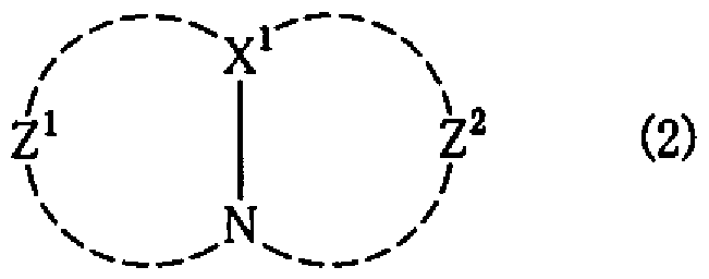
- X 1 represents a carbon atom or a nitrogen atom
- Z 1 and Z 2 each independently represent a nitrogen-containing heteroatom. Represents an atom group capable of forming a ring.
- the electron transporting material has a nitrogen-containing aromatic polycyclic group consisting of a five-membered ring or a six-membered ring, and has a plurality of nitrogen atoms, it has a skeleton having a nitrogen atom at an adjacent ⁇ bond position 5.
- the organic EL device according to any one of items 1 to 4, which is an organic compound.
- the organic electroluminescent device according to any one of 1 to 5, wherein the electron transporting material or the host material is a compound having one carbazolyl group or one tetrahydrocarbazolyl group.
- the electron transporting material or the host material is a compound having a carbazolyl group or a tetrahydrocarbazolyl group, and a nitrogen-containing heterocyclic group.
- Luminescent element is a compound having a carbazolyl group or a tetrahydrocarbazolyl group, and a nitrogen-containing heterocyclic group.
- the organic EL device according to any one of items 1 to 9, having a plurality of electron transport layers.
- Optical energy gap value (Eg) force of the electron transporting material forming each layer of the plurality of electron transporting layers The feature is that the electron transporting layer, which forms an interface with the light emitting layer, is equal or smaller from the electron transporting layer toward the cathode.
- the triplet energy gap value of the electron transporting material forming each layer of the plurality of electron transporting layers is equal or smaller from the electron transporting layer forming the interface with the light emitting layer toward the cathode.
- the organic EL device according to any one of 10 to 12.
- the triplet energy gap value of the electron transport material forming the electron transport layer forming an interface with the light emitting layer is larger than the triplet energy gap value of the metal complex compound of the light emitting layer. 13.
- the host material forming the light emitting layer is a main material of the light emitting layer, and the metal complex compound having a phosphorescent light emitting property and a heavy metal functions as a light emitting dopant.
- the electron transport layer is located on the cathode side between the cathode and the anode.
- the conditional expression regarding ⁇ is satisfied.
- the number of electron transport layers is plural, it is more preferable to satisfy at least the condition regarding ⁇ ⁇ ⁇ ⁇ ⁇ ⁇ ⁇ , and it is more preferable to satisfy the conditional expression regarding ⁇ ′ between at least one adjacent two electron transport layers. It is further preferable that the conditional expression regarding ⁇ ′ be satisfied between all two adjacent electron transport layers. The same applies to a case where there are a plurality of light emitting layers.
- a phosphorescent organic EL element having a low voltage and a high current efficiency, particularly an organic EL element in a blue light emitting region.
- FIG. 1 is a diagram of the organic EL device of Example 1-6.
- the organic EL device of the present invention is an organic EL device having a laminated structure including at least a light emitting layer and an electron transport layer between a cathode and an anode.
- the light emitting layer and the electron transport layer may be a single layer or a plurality of layers.
- the organic EL device of the present invention provides a triplet energy gap of a host material forming a light emitting layer.
- Value (Eg T ) is 2.52 eV or more and 3.7 eV or less, preferably 2.75 eV or more and 3.7 eV or less, more preferably 2.80 eV or more and 3.7 eV or less, and particularly preferably 2.9 eV or more and 3.7 eV or less. More preferably, it is 3.3 eV or more and 3.7 eV or less.
- the electron transporting material forming the electron transporting layer is a material different from the host material and has a hole transporting ability.
- the electron transporting material has hole transporting ability! /" Means that the electron transporting material can measure the hole mobility.
- a time of flight method (a method of calculating a measuring force of a traveling time of a charge in an organic film) can be used.
- the time characteristics of the transient current from the electrode / organic layer (layer made of an organic material forming the electron transporting layer) / electrode configuration
- the following equation force also calculates the hole mobility.
- the electron mobility can be measured.
- Electric field strength (applied voltage to device) Z (organic layer thickness)
- the hole mobility (h) of the electron transporting material measured by the time of flight method in the electric field strength of 10 5 to 10 7 VZcm is 1.0 X 10— ⁇ n ⁇ / iV. It is preferable to show 'sX / z (h). Particular preference is given to exhibit 1. 0 X 10- 5 cm 2 / (V 's) greater than.
- the organic EL device of the present invention further includes a metal complex compound (light emitting dopant) having a phosphorescent light emitting property and a heavy metal in the light emitting layer.
- a metal complex compound light emitting dopant
- the present invention is characterized in that the luminescent dopant emits light due to a triplet energy gap in the organic EL device. As a result, the recombination energy of holes and electrons in the organic EL element moves to the light emitting dopant more efficiently, and leads to light emission.
- the ion transport potential of the electron transport material forming the electron transport layer is preferably 5.6e
- ⁇ is set in this range, accumulation of holes due to a difference in ionization potential between the light emitting layer and the electron transport layer can be avoided, and a higher voltage can be suppressed.
- the difference ( ⁇ ′) between the ion transport potentials of the electron transport materials forming each layer is represented by the following formula. ) Is preferably ⁇ 0.2 eV ⁇ ′ ⁇ 0.4 eV, more preferably ⁇ 0.2 eV ⁇ ′ ⁇ 0.2 eV.
- Ip (i) The ionization potential of the electron transporting material forming the i-th layer (i is an integer of 1 or more and (N-1) or less) viewed from the light-emitting layer.
- the optical energy gap value (Eg) of the electron transporting material forming each layer of the electron transporting layer is determined at the interface between the light emitting layer and the light emitting layer. It is preferable that the electron transport layer to be formed is equal or smaller from the electron transport layer toward the cathode, that is, in the electron transport layer having the N-layer structure, the following relationship is satisfied.
- the triplet energy gap value (Eg T ) of the electron transport material forming each of the electron transport layers is determined by the light emission.
- Layers and It is preferable that the electron transport layer forming the interface is equal or smaller toward the cathode, that is, the following relationship is satisfied in the electron transport layer having the N-layer structure.
- Eg T (x) triplet energy gap value of the electron transport layer in the x-th layer (X is an integer from 1 to N) as viewed from the light-emitting layer
- the triplet energy gap value of the luminescent dopant in the light emitting layer is Eg T (dopant)
- Eg T (1) triplet energy gap value of the electron transport layer that forms an interface with the light emitting layer
- the host material, luminescent dopant, and electron transport material used in the organic EL device of the present invention are not particularly limited as long as they are selected so as to satisfy the above conditions.
- Preferred host materials include, for example, fluorescent brighteners such as amamine derivatives, phorazole derivatives, oxadiazole derivatives, triazole derivatives, benzoxazoles, benzothiazoles and benzoimidazoles, metal chelates and oxanioids. And conjugates having good thin film forming properties such as styryl compounds.
- fluorescent brighteners such as amamine derivatives, phorazole derivatives, oxadiazole derivatives, triazole derivatives, benzoxazoles, benzothiazoles and benzoimidazoles, metal chelates and oxanioids.
- metal chelates such as styryl compounds.
- conjugates having good thin film forming properties such as styryl compounds.
- an electron transport material described later may be used as a host material.
- the luminescent dopant preferably functions as a luminescent dopant that emits light from a triplet at room temperature.
- Preferred examples of the heavy metal contained in the dopant include Ir, Pt, Pd, Ru, Rh, Mo, and Re.
- heavy metal ligands include, for example, ligands in which C and N are coordinated or bonded to a metal (CN ligand). More specifically,
- substituent of the substituted derivative include an alkyl group, an alkoxy group, a phenyl group, a polyphenyl group or a naphthyl group, a fluoro (F) group, a trifluoromethyl group (CF) group, and the like.
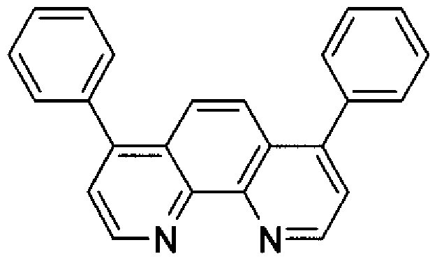
- the material used for the electron transporting material is preferably at least an electron-deficient nitrogen-containing five-membered ring derivative or a nitrogen-containing six-membered ring derivative.
- electron deficiency means, for example, one in which one or more carbons of a 6 ⁇ aromatic ring are changed to nitrogen.
- Preferred electron transporting materials include those having at least one of the following structures (1) and (3).
- x 1 represents a carbon atom or a nitrogen atom
- z 1 and z 2 are each independently represent a formable atomic group the nitrogen-containing heterocycle.
- any one or more of the above structures (1) and (3) has a five-membered or eighteen-membered ring, preferably a five- or six-membered ring-containing nitrogen-containing compound.
- an aromatic polycyclic group is formed and a plurality of nitrogen atoms are present, an organic compound having a skeleton having a nitrogen atom at a non-adjacent bond position can be used.
- a carbazolyl group a pyridyl group, a pyrimidinyl group, a pyrazyl group, a triazinyl group, a quinoxalyl group, a quinolyl group, an imidazolyl group, a triazolyl group, a tetrazolyl group, an oxdiazolyl group, a thiadiazolyl group, or an oxatriazolyl group
- a compound having ⁇ ), which may also have a substituent, is preferred.
- R 1 to R 5 indicate a bonding position where the group is bonded, and R 1 and R 2 , R 3 and R 4 , and R 2 and R 3 may be a ring.
- Y 1 and Y 2 are carbon or nitrogen (both do not simultaneously take nitrogen). When Y 1 or Y 2 is nitrogen, there is no R 2 or R 3 respectively.
- At least one of RR 4 and R 5 in the above formula (4) is a nitrogen or an aromatic ring.
- a conjugated compound linked to at least another skeleton represented by the above formula (4) via at least one nitrogen or aromatic ring and via an alicyclic compound is also preferable.
- the skeletal group represented by the following formula is referred to as a tetrahydrocarbazolyl group.
- Y is a substituted or unsubstituted aryl group having 6 to 40 carbon atoms, a substituted or unsubstituted heterocyclic group having 3 to 40 carbon atoms, a linear or branched substituted or unsubstituted carbon atom having 1 to 4 carbon atoms, An alkyl group of 30; a substituted or unsubstituted cycloalkyl group having 5 to 40 carbon atoms;
- L is a substituted or unsubstituted arylene group having 6 to 40 carbon atoms, a divalent substituted or unsubstituted heterocyclic group having 3 to 40 carbon atoms, a straight-chain or branched substituted or unsubstituted carbon atom, An alkylene group of 30 or a substituted or unsubstituted cycloalkylene group having 5 to 40 carbon atoms,
- L ' is a trivalent substituted or unsubstituted aryl group having 6 to 40 carbon atoms, a trivalent substituted or unsubstituted heterocyclic group having 3 to 40 carbon atoms, trivalent linear or branched substituted Or an unsubstituted alkyl group having 1 to 30 carbon atoms, or a trivalent substituted or unsubstituted cycloalkyl group having 5 to 40 carbon atoms.
- X 3 —X 6 are each independently represented by hydrogen, Y—, Y—L or Y—L, (—Y) —, and the definitions of Y, L and L ′ are as described above.
- R 6 to R 13 each independently represent hydrogen, a halogen atom, a cyano group, a silyl group, a substituted or unsubstituted amino group, a substituted or unsubstituted aryl group having 6 to 40 carbon atoms, a substituted or unsubstituted aryl group, An unsubstituted aryloxy group having 6 to 40 carbon atoms, a substituted or unsubstituted heterocyclic group having 3 to 40 carbon atoms, a linear or branched substituted or unsubstituted alkyl group having 1 to 30 carbon atoms, It is a substituted or unsubstituted alkoxy group having 1 to 30 carbon atoms, a substituted or unsubstituted aralkyl group having 7 to 40 carbon atoms, or a substituted or unsubstituted cycloalkyl group having 5 to 40 carbon atoms.
- Examples of the substituted or unsubstituted aryl group of Y include phenyl, 1 naphthyl, 2 naphthyl, 1 anthryl, 2 anthryl, 9 anthryl, 1 phenanthryl, 2 phenanthryl, 3 phenanthryl group, 4-phenanthryl group, 9-phenanthryl group, 1 naphthacyl group, 2 naphthacyl group, 9 naphthacyl group, 1-pyrenyl group, 2-pyrenyl group, 4-pyrenyl group, 2-biphenyl-yl group, 3-biphenyl-yl group, 4-biphenyl-yl group, ⁇ -tert-yl 4-yl group, p-tertyl 3-yl group, p-tertyl 2-yl group , M terfel 4-yl group, m terfel 3-yl group, m terfel 2-yl group, o-tolyl group, m-tolyl group, ⁇
- Examples of the substituted or unsubstituted heterocyclic group for Y include pyrrole, pyridine, pyrimidine, pyrazine, triazine, aziridine, azaindolizine, indolizine, imidazole, indole, isoindole, indazole, purine, pteridine, j8-carboline and the like.
- Examples of the substituted or unsubstituted alkyl group for Y include a methyl group, a trifluoromethyl group, an ethyl group, a propyl group, an isopropyl group, an n-butyl group, an s-butyl group, an isobutyl group, a t-butyl group, n pentyl group, n-hexyl group, n-heptyl group, n-aminobutyl group, hydroxymethyl group, 1-hydroxyethyl group, 2-hydroxyethyl group, 2-hydroxyisobutyl group, 1, 2-dihydroxyethyl group, 1,3-dihydroxyisopropyl group, 2,3-dihydroxymethyl butyl group, 1,2,3-trihydroxypropyl group, chloromethyl group, 1-chloroethyl group, 2-chloroethyl group , 2-chloroisobutyl, 1,2-dichloroethyl
- Examples of the substituted or unsubstituted cycloalkyl group for Y include a cyclopentyl group, a cyclohexyl group, a 4-methylcyclohexyl group, an adamantyl group, a norbornyl group and the like.
- Examples of the substituted or unsubstituted arylene group for L include those in which the above-mentioned substituted or unsubstituted aryl group is a divalent group.
- Examples of the divalent substituted or unsubstituted heterocyclic group having 3 to 40 carbon atoms of L include those obtained by converting the above-mentioned substituted or unsubstituted heterocyclic group into a divalent or higher valent group.
- Examples of the substituted or unsubstituted alkylene group for L include those in which the above-described substituted or unsubstituted alkyl group is a divalent group.
- Examples of the substituted or unsubstituted cycloalkylene group for L include those in which the above-mentioned substituted or unsubstituted cycloalkyl group is a divalent group.
- V examples include those in which the above-mentioned exemplified group of Y is trivalent.
- halogen atom of R 6 to R 13 examples include fluorine, chlorine, bromine, iodine and the like.
- Examples of the substituted or unsubstituted aryl group of R 6 to R 13 are the same as those described above for Y.
- the substituted or unsubstituted aryloxy group of R 6 — R 13 is represented by OP, and examples of P Are phenyl, 1 naphthyl, 2 naphthyl, 1 anthryl, 2 anthryl, 9—anthryl, 1 phenanthryl, 2 phenanthryl, 3-phenanthryl, 4-phenanthryl, 9 phenanthryl , 1 naphthacyl group, 2 naphthacyl group, 9 naphthacyl group, 1-pyryl group, 2-pyryl group, 4-pyryl group, 2-biphenyl group, 3-biphenyl Ruyl group, 4-biphenyl-yl group, p-terfyl 4-yl group, p-terfyl 2-ru 3-yl group, p-terfel-ru 2-yl group, m-terfel-ru 4-yl group, m-terfure Ru-3-yl group, m-terphenyl-2-yl group,
- Examples of the substituted or unsubstituted heterocyclic group, alkyl group and cycloalkyl group for R 6 to R 13 include the same as those described above for Y.
- the substituted or unsubstituted alkoxy group represented by R 6 to R 13 is a group represented by OQ, and examples of Q include the same as the substituted or unsubstituted alkyl group described above for Y. .
- Examples of the substituted or unsubstituted aralkyl group of R 6 —R 13 include a benzyl group, a 1-phenyl-ethyl group, a 2-phenyl-ethyl group, a 1-phenyl-isopropyl group, and a 2-phenyl-isopropyl group.
- Pill group ferru-t-butyl group, ⁇ -naphthylmethyl group, 1- ⁇ -naphthylethyl group, 2- ⁇ -naphthylethyl group, l- ⁇ -naphthylisopropyl group, 2- ⁇ -naphthylisopropyl pill group, j8-naphthylmethyl group, 1 j8 —Naphthylethyl group, 2j8-naphthylethyl group, 1-J8-naphthylisopropyl group, 2j8-naphthylisopropyl group, 1 pyrrolylmethyl group, 2- (1pyrrolyl) ethyl group, p-methylbenzyl group, m-methylbenzyl group, o —Methyl benzodinole, p-methyl benzene, o-methyl benzene, o chloro-
- the electron transporting material or the host material is preferably a compound having at least one group selected from carbazolyl and tetrahydrocarbazolyl. More preferably, it is a compound having one or two groups.
- the electron transporting material or the host material may further have a nitrogen-containing heterocyclic group.
- a more specific example of the compound represented by the above formula (4) is exemplified in Japanese Patent Application No. 2002-305375.
- R 14 to R 18 represent a hydrogen atom or a substituent having 1 to 40 carbon atoms, and R 14 and R la may combine with each other to form a saturated or unsaturated cyclic structure.
- R ′ represents an alkyl group or an aryl group.
- a preferred alkyl group is a methyl group or an ethyl group
- a preferred aryl group is a phenyl group
- n is an integer of 3- 8
- Z 3 is 0, NR 2G or S
- R 19 and R 2G is, individually, hydrogen, propyl, t-butyl group, 1, such as heptyl (I) an alkyl group having 24 carbon atoms; an aryl or hetero atom having 5-20 carbon atoms such as phenyl, naphthyl, furyl, phenyl, phenyl, pyridyl, quinolyl, and other heterocyclic systems.
- examples thereof include a benzimidazole derivative described in Japanese Patent Application No. 2003-067847 and a metal complex described in US Pat. No. 5,141,671.
- a compound having a carbazolyl group is preferred.
- organic compounds having a carbazolyl group and a substituted or unsubstituted pyridyl group, virazyl group, pyrimidyl group, triazyl group, amino group or oxaziazol group.
- the nitrogen heterocyclic group may be substituted or unsubstituted.
- Examples of the powerful compound include a compound represented by the following formula.
- Cz is a substituted or unsubstituted arylcarbazolyl group or carbazolylalkylene group
- A is a group represented by the following formula.
- M and M ′ are each independently a nitrogen-containing heteroaromatic ring having 2 to 40 carbon atoms forming a substituted or unsubstituted ring, and may be the same or different.
- P is 0-2, q is 1-2, r is an integer of 0-2, where p + r is 1 or more.
- Examples include compounds containing a rivazolyl group and a nitrogen-containing heterocyclic group.
- the electron transport materials listed here may be used as a host material of the light emitting layer.
- the configuration of the organic EL device of the present invention includes, for example, the following (a)-( ⁇ ).
- the light emitting layer in the organic EL device of the present invention is a layer obtained by adding a light emitting dopant to the above-described host material.
- the addition concentration of the luminescent dopant is not particularly limited, but for adjustment of current efficiency and driving voltage, 0.1 to 20% by weight is preferable, and 1 to 15% by weight is more preferable. .
- the organic EL device of the present invention is preferably supported by a substrate. Also, on the substrate
- the layers from the anode to the cathode may be laminated sequentially, or the layers from the cathode to the anode may be laminated sequentially.
- At least one of the anode and the cathode is formed of a transparent or translucent substance.
- the material of the substrate used in the present invention is not particularly limited, and a material commonly used in a known organic EL device, for example, a material having high strength such as glass, transparent plastic, or quartz can be used.
- a metal, an alloy, an electrically conductive compound or a mixture thereof having a large work function force eV or more is preferably used.
- Specific examples include metals such as Au and dielectric transparent materials such as Cul, ITO, SnO and ZnO.
- the anode can be manufactured by forming a thin film of the above material by a method such as a vapor deposition method or a sputtering method.
- the transmittance of the anode is preferably greater than 10%.
- the sheet resistance of the anode is preferably several hundred ⁇ / square or less.
- the thickness of the anode depends on the material, and is usually in the range of 10 nm to 1 ⁇ m, preferably 10 to 200 nm. Selected by box.
- a metal, an alloy, an electrically conductive conjugate, or a mixture thereof having a work function force of eV or less is preferably used.
- Specific examples include sodium, lithium, aluminum, a magnesium / silver mixture, a magnesium Z copper mixture, A1 ZA1 O, indium, and the like.
- the cathode can be manufactured by forming a thin film of the above material by a method such as an evaporation method or a sputtering method.
- the transmittance of the cathode is preferably greater than 10%.
- the sheet resistance of the cathode is preferably not more than several hundred ⁇ / square.
- the thickness of the cathode is selected depending on the material, usually in the range of lOnm-1 ⁇ m, preferably in the range of 50-200 nm.
- the organic EL device of the present invention may be provided with a hole injection layer, a hole transport layer, an electron injection layer, and the like, if necessary, to further increase the current (or light emission) efficiency.
- the materials used for these layers are not particularly limited, and organic materials known as conventional organic EL materials can be used. Specific examples include an amine derivative, a stilbene derivative, a silazane derivative, and a polysilane / aniline copolymer.
- an inorganic material to the hole injection layer, the hole transport layer, and the electron injection layer.
- the inorganic material include a metal oxide and the like.
- an inorganic material may be used between the electron transport layer and the metal cathode in order to increase the current (or light emission) efficiency.
- the inorganic material include fluorides and oxides of alkali metals such as Li, Mg, and Cs.
- the method for manufacturing the organic EL device of the present invention is not particularly limited, and the organic EL device can be manufactured using a manufacturing method used for a conventional organic EL device.
- each layer can be formed by a vacuum deposition method, a casting method, a coating method, a spin coating method, or the like.
- the organic material of each layer is dispersed in a transparent polymer such as polycarbonate, polyurethane, polystyrene, polyarylate, and polyesterol
- the organic material and the transparent polymer can be used. It can also be manufactured by simultaneous vapor deposition or the like.
- the material is irradiated with light (excitation light) from a deuterium lamp that has been spectrally analyzed by a monochromator, the emitted photoelectron emission is measured by an electometer, and the photoelectron emission threshold of the obtained photoelectron emission is calculated from a curve Was measured by the external method.
- an atmospheric ultraviolet photoelectron analyzer AC-1 manufactured by Riken Keiki Co., Ltd. was used.
- the wavelength-resolved light was irradiated to a toluene dilute solution of each material, and the light was converted from the longest wavelength of the absorption spectrum.
- a spectrophotometer (U-3400 (trade name), manufactured by Hitachi) was used as a measuring instrument.
- the triplet energy gap (Eg T (Doapnt) was determined by the following method.
- the sample placed in the quartz cell was cooled to 77 K, irradiated with excitation light, and measured for the phosphorescence with respect to wavelength.
- the value obtained by converting the wavelength value into an energy value was defined as Eg T.
- the measurement was performed using the Hitachi F-4500 Model Spectrofluorimeter main unit and optional equipment for low-temperature measurement. Alternatively, measurement may be performed by combining a low-temperature container with an excitation light source and a light receiving device. In this example, the wavelength was converted by the following equation.
- the ⁇ edge '' means that when the phosphorescence spectrum is represented by taking the phosphorescence intensity on the vertical axis and the wavelength on the horizontal axis, draw a tangent to the rise of the phosphorescence spectrum on the short wavelength side, and draw the tangent and the horizontal axis. Means the wavelength value at the intersection of. Unit: nm.
- the organic EL device shown in FIG. 1 was manufactured as follows.
- ITO transparent electrode (anode) 12 glass substrate 11 manufactured by Geomatic was subjected to ultrasonic cleaning in isopropyl alcohol for 5 minutes, and then UV ozone cleaning for 30 minutes. .
- the glass substrate 11 with the transparent electrode lines after cleaning is mounted on a substrate holder of a vacuum evaporation apparatus. First, on the surface on the side where the transparent electrode lines are formed, cover the transparent electrodes 12 so as to have a film thickness of 100 nm.
- TPD232 film 13 was formed by resistance heating evaporation.
- the TPD232 film 13 functions as a hole injection layer (hole transport layer).
- HTM hole transport layer
- a hole transport layer (HTM) 14 having a film thickness of lOnm was formed on the film by resistance heating evaporation.
- FIrpic concentration was 7.5 Wt%.
- This Host No 1: FIrpic film 15 functions as a light emitting layer.
- the electron transport materials ETM—No. 1 (Example 1), ETM—No. 2 (Example 2) shown in Table 1 ), ETM—No. 3 (Example 3), PC-7 (Example 4), and 8-hydroxyquinolinol aluminum complex (Alq) (Example 5) to resist the electron transport layer 16 having a thickness of 30 nm.
- a film was formed by heating evaporation.
- LiF was used as the electron injecting electrode (cathode) 17 to form a film having a thickness of 0.1 Inm at a film forming rate of 1 AZmin.
- metal A1 was vapor-deposited, and a metal cathode 18 was formed to a thickness of 130 nm to form an organic EL light emitting device 100.
- An organic EL light emitting device was manufactured in the same manner as in Example 1, except that the following compound was used as an electron transporting material in the same device configuration as in Example 1.
- a 25 mm ⁇ 75 mm ⁇ 1.1 mm thick glass substrate with an ITO transparent electrode (manufactured by Geomatic) was subjected to ultrasonic cleaning in isopropyl alcohol for 5 minutes, and then to UV ozone cleaning for 30 minutes.
- the glass substrate with the transparent electrode lines after cleaning is mounted on the substrate holder of the vacuum evaporation apparatus.
- the TPD232 having a film thickness of lOOnm is coated on the side where the transparent electrode lines are formed so as to cover the transparent electrodes.
- the film was formed by resistance heating evaporation.
- This TPD232 film functions as a hole injection layer (hole transport layer).
- HTM hole transport layer
- a host material Host No. 1
- FIrpic luminescent dopant
- the electron transporting materials ETM—No. 1 (Example 6) and ETM—No. 3 (Example 7) shown in Table 2 were used on this light emitting layer. Then, a 20 nm-thick electron transport layer was formed by resistance heating evaporation.
- Alq was deposited to a thickness of 10 nm to further form an electron transport layer.
- LiF was used as an electron injecting electrode (cathode) to form a film having a thickness of 0.1 Inm at a film forming rate of lAZmin.
- a metal A1 was deposited on this LiF layer, a metal cathode was formed to a thickness of 130 nm, and an organic EL light emitting device was formed and evaluated. Table 2 shows the results.
- Example 6 an organic EL light emitting device was manufactured by the same device configuration and manufacturing process as in Example 6, except that ETM-No. 3 was used instead of Alq. Table 2 shows the evaluation results.
- Example 9 In Example 7, the same steps were performed up to the formation of ETM-No. 3, and thereafter, Alq was further formed into a film having a thickness of lOnm to form an electron transport layer.
- LiF was used as an electron injecting electrode (cathode) to form a film having a thickness of 0.1 Inm at a film forming rate of lAZmin.
- metal A1 was vapor-deposited, and a metal cathode was formed to a thickness of 130 nm to produce an organic EL light emitting device.
- Table 2 shows the evaluation results.
- the upper material forms the electron transport layer on the metal electrode side, and the lower material forms the electron transport layer that forms an interface with the light emitting layer.
- Example 6 an organic EL light emitting device was manufactured by the same device configuration and manufacturing process as in Example 6, except that the following ETM—No. 4—ETM—No. 12 was used instead of ETM—No. . Table 3 shows the evaluation results.
- the organic EL device of the present invention has high luminous efficiency and low power consumption even at high luminance, It can be used in fields such as information display devices, in-vehicle display devices, and lighting. Specifically, it can be suitably used as a light source such as a flat light-emitting body of a wall-mounted television or a knock light of a display.
Abstract
Description


Claims
Priority Applications (4)
| Application Number | Priority Date | Filing Date | Title |
|---|---|---|---|
| JP2005517777A JP5179720B2 (en) | 2004-02-09 | 2005-02-08 | Organic electroluminescence device |
| KR1020067015981A KR101159373B1 (en) | 2004-02-09 | 2005-02-08 | Organic electroluminescent device |
| US10/588,549 US20070257600A1 (en) | 2004-02-09 | 2005-02-08 | Organic Electroluminescent Device |
| EP05709851.9A EP1718121B1 (en) | 2004-02-09 | 2005-02-08 | Organic electroluminescent device |
Applications Claiming Priority (2)
| Application Number | Priority Date | Filing Date | Title |
|---|---|---|---|
| JP2004032542 | 2004-02-09 | ||
| JP2004-032542 | 2004-02-09 |
Publications (1)
| Publication Number | Publication Date |
|---|---|
| WO2005076669A1 true WO2005076669A1 (en) | 2005-08-18 |
Family
ID=34836092
Family Applications (1)
| Application Number | Title | Priority Date | Filing Date |
|---|---|---|---|
| PCT/JP2005/001799 WO2005076669A1 (en) | 2004-02-09 | 2005-02-08 | Organic electroluminescent device |
Country Status (7)
| Country | Link |
|---|---|
| US (1) | US20070257600A1 (en) |
| EP (1) | EP1718121B1 (en) |
| JP (1) | JP5179720B2 (en) |
| KR (1) | KR101159373B1 (en) |
| CN (1) | CN100591183C (en) |
| TW (1) | TWI428053B (en) |
| WO (1) | WO2005076669A1 (en) |
Cited By (43)
| Publication number | Priority date | Publication date | Assignee | Title |
|---|---|---|---|---|
| JP2006049570A (en) * | 2004-08-04 | 2006-02-16 | Chisso Corp | Organic electroluminous element |
| WO2006049013A1 (en) * | 2004-11-04 | 2006-05-11 | Idemitsu Kosan Co., Ltd. | Compound containing fused ring and organic electroluminescent element employing the same |
| WO2006062062A1 (en) * | 2004-12-10 | 2006-06-15 | Pioneer Corporation | Organic compound, charge-transporting material, and organic electroluminescent element |
| JP2006156445A (en) * | 2004-11-25 | 2006-06-15 | Konica Minolta Holdings Inc | Organic electroluminescent element, display device and lighting system |
| WO2006067976A1 (en) * | 2004-12-24 | 2006-06-29 | Pioneer Corporation | Organic compound, charge-transporting material, and organic electroluminescent element |
| JP2006188493A (en) * | 2004-12-10 | 2006-07-20 | Pioneer Electronic Corp | Organic compound, charge transport material and organic electroluminescent element |
| WO2007029402A1 (en) * | 2005-09-08 | 2007-03-15 | Idemitsu Kosan Co., Ltd. | Organic electroluminescence device |
| WO2007029403A1 (en) * | 2005-09-08 | 2007-03-15 | Idemitsu Kosan Co., Ltd. | Organic electroluminescence device |
| JP2007137829A (en) * | 2005-11-18 | 2007-06-07 | Chemiprokasei Kaisha Ltd | New triazine derivative and organic electroluminescence element using the same |
| JP2009035524A (en) * | 2007-08-03 | 2009-02-19 | Chemiprokasei Kaisha Ltd | New bicarbazole derivative, and host material and organic electroluminescent element each using the same |
| JP2009158848A (en) * | 2007-12-27 | 2009-07-16 | Idemitsu Kosan Co Ltd | Material for organic electroluminescent element, and organic electroluminescent element using the material |
| JP2010013421A (en) * | 2008-07-07 | 2010-01-21 | Chemiprokasei Kaisha Ltd | New bis(dicarbazolylphenyl) derivative, host material using the same and organic electroluminescencent device |
| JP2010030937A (en) * | 2008-07-28 | 2010-02-12 | Chemiprokasei Kaisha Ltd | New dicarbazolylphenyl derivative, host material obtained by using the same, and organic electroluminescent element |
| WO2010044607A1 (en) * | 2008-10-14 | 2010-04-22 | Cheil Industries Inc. | Benzimidazole compounds and organic photoelectric device with the same |
| WO2010047279A1 (en) * | 2008-10-23 | 2010-04-29 | 富士フイルム株式会社 | Organic electroluminescent element |
| WO2010084690A1 (en) * | 2009-01-22 | 2010-07-29 | 富士フイルム株式会社 | Organic electroluminescent element |
| JP2010171363A (en) * | 2008-12-24 | 2010-08-05 | Idemitsu Kosan Co Ltd | Organic el device |
| WO2010137411A1 (en) * | 2009-05-29 | 2010-12-02 | Fujifilm Corporation | Organic electroluminescence element |
| JP2011084553A (en) * | 2009-09-15 | 2011-04-28 | Tosoh Corp | Pyrimidine derivative, production method therefor, and organic electroluminescent element including the same as constituent |
| WO2011083588A1 (en) | 2010-01-08 | 2011-07-14 | 三菱化学株式会社 | Organic el element and organic light-emitting device |
| JP2011142096A (en) * | 2009-07-31 | 2011-07-21 | Fujifilm Corp | Container containing material for organic electroluminescent element, material for organic electroluminescent element, vapor deposition film and its manufacturing method, and organic electroluminescent element |
| JP2011176333A (en) * | 2011-04-01 | 2011-09-08 | Konica Minolta Holdings Inc | Organic electroluminescent element, display device and lighting device |
| WO2011148909A1 (en) * | 2010-05-24 | 2011-12-01 | 出光興産株式会社 | Organic electroluminescent element |
| WO2012070234A1 (en) * | 2010-11-22 | 2012-05-31 | Idemitsu Kosan Co.,Ltd. | Organic electroluminescence device |
| JP2012513987A (en) * | 2008-12-24 | 2012-06-21 | チェイル インダストリーズ インコーポレイテッド | Novel compound for organic photoelectric device and organic photoelectric device including the same |
| WO2012086170A1 (en) * | 2010-12-20 | 2012-06-28 | 出光興産株式会社 | Aromatic heterocycle derivative and organic electroluminescent element using same |
| JP2013048265A (en) * | 2005-03-31 | 2013-03-07 | Trustees Of Princeton Univ | Oled utilizing direct injection to triplet state |
| JP2013084965A (en) * | 2012-11-26 | 2013-05-09 | Konica Minolta Holdings Inc | Organic electroluminescent element, display device, and lighting device |
| WO2013069762A1 (en) * | 2011-11-11 | 2013-05-16 | 東ソー株式会社 | Cyclic azine compound having nitrogen-containing fused aromatic group, method for producing same, and organic electroluminescent element using same as constituent component |
| JP2013526773A (en) * | 2010-05-11 | 2013-06-24 | メルク パテント ゲーエムベーハー | Organic electroluminescence device |
| JP2013234187A (en) * | 2007-05-17 | 2013-11-21 | Semiconductor Energy Lab Co Ltd | Substance, light-emitting element, lighting device, light-emitting device, and electronic device |
| JP2014507401A (en) * | 2010-12-20 | 2014-03-27 | イー・アイ・デュポン・ドウ・ヌムール・アンド・カンパニー | Triazine derivatives for electronics applications |
| WO2014073307A1 (en) * | 2012-11-07 | 2014-05-15 | 出光興産株式会社 | Organic electroluminescent element and electronic device |
| WO2014133121A1 (en) | 2013-03-01 | 2014-09-04 | 国立大学法人九州大学 | Compound, light-emitting material, and organic light-emitting element |
| WO2014157230A1 (en) * | 2013-03-25 | 2014-10-02 | 出光興産株式会社 | Organic electroluminescent element and manufacturing method therefor |
| JP2014197696A (en) * | 2006-05-17 | 2014-10-16 | 三菱化学株式会社 | Composition for organic electroluminescent element |
| US8883323B2 (en) | 2010-11-22 | 2014-11-11 | Idemitsu Kosan Co., Ltd. | Organic electroluminescence device |
| US8933622B2 (en) | 2005-05-24 | 2015-01-13 | Pioneer Corporation | Organic electroluminescence element |
| WO2015072520A1 (en) * | 2013-11-13 | 2015-05-21 | 出光興産株式会社 | Compound, material for organic electroluminescent element, organic electroluminescent element, and electronic device |
| US9324950B2 (en) | 2010-11-22 | 2016-04-26 | Idemitsu Kosan Co., Ltd. | Organic electroluminescence device |
| WO2016117429A1 (en) * | 2015-01-20 | 2016-07-28 | 保土谷化学工業株式会社 | Pyrimidine derivative and organic electroluminescence element |
| JP2016189468A (en) * | 2010-07-30 | 2016-11-04 | ローム・アンド・ハース・エレクトロニック・マテリアルズ・コリア・リミテッド | Electroluminescent device employing electroluminescent compound as light emitting material |
| US20170335181A1 (en) * | 2014-10-23 | 2017-11-23 | Rohm And Haas Electronic Materials Korea Ltd. | A novel combination of a host compound and a dopant compound and an organic electroluminescent device comprising the same |
Families Citing this family (32)
| Publication number | Priority date | Publication date | Assignee | Title |
|---|---|---|---|---|
| TW200541401A (en) * | 2004-02-13 | 2005-12-16 | Idemitsu Kosan Co | Organic electroluminescent device |
| WO2005085387A1 (en) * | 2004-03-08 | 2005-09-15 | Idemitsu Kosan Co., Ltd. | Material for organic electroluminescence device and organic electroluminescence device utilizing the same |
| WO2005112519A1 (en) * | 2004-05-14 | 2005-11-24 | Idemitsu Kosan Co., Ltd. | Organic electroluminescent device |
| US7651791B2 (en) | 2005-12-15 | 2010-01-26 | Idemitsu Kosan Co., Ltd. | Material for organic electroluminescence device and electroluminescence device employing the same |
| EP2138486B2 (en) * | 2007-03-26 | 2022-10-19 | NIPPON STEEL Chemical & Material Co., Ltd. | Organic electroluminescent device |
| KR20090024998A (en) * | 2007-09-05 | 2009-03-10 | 제일모직주식회사 | Material for organic photoelectric device comprising electron transporting unit and hole transporting unit, and organic photoelectric device thereby |
| CN101868868A (en) | 2007-11-22 | 2010-10-20 | 出光兴产株式会社 | Organic el element |
| WO2009081857A1 (en) * | 2007-12-21 | 2009-07-02 | Idemitsu Kosan Co., Ltd. | Organic electroluminescent device |
| EP2123733B1 (en) | 2008-05-13 | 2013-07-24 | Konica Minolta Holdings, Inc. | Organic electroluminescent element, display device and lighting device |
| KR101233375B1 (en) * | 2008-12-24 | 2013-02-15 | 제일모직주식회사 | Novel compound for organic photoelectric device and organic photoelectric device including the same |
| KR101233377B1 (en) | 2008-12-30 | 2013-02-18 | 제일모직주식회사 | Novel compound for organic photoelectricand organic photoelectric device including the same |
| CN102272262B (en) * | 2008-12-30 | 2014-09-10 | 第一毛织株式会社 | Novel compounds for an organic photoelectric device, and organic photoelectric device comprising same |
| EP2415773B1 (en) * | 2009-03-30 | 2016-02-17 | Duk San Neolux Co., Ltd. | Organic electronic device, compounds for same, and terminal |
| US8039129B2 (en) | 2009-04-06 | 2011-10-18 | Idemitsu Kosan Co., Ltd. | Organic electroluminescence device and material for organic electroluminescence device |
| US8039127B2 (en) * | 2009-04-06 | 2011-10-18 | Idemitsu Kosan Co., Ltd. | Organic electroluminescence device and material for organic electroluminescence device |
| EP2489664A4 (en) | 2009-10-16 | 2013-04-03 | Idemitsu Kosan Co | Fluorene-containing aromatic compound, material for organic electroluminescent element, and organic electroluminescent element using same |
| KR101288566B1 (en) | 2009-12-16 | 2013-07-22 | 제일모직주식회사 | Compound for organic photoelectric device and organic photoelectric device including the same |
| US8617720B2 (en) | 2009-12-21 | 2013-12-31 | E I Du Pont De Nemours And Company | Electroactive composition and electronic device made with the composition |
| KR101297158B1 (en) * | 2010-02-22 | 2013-08-21 | 제일모직주식회사 | Compound for organic photoelectric device and organic photoelectric device including the same |
| JP4751954B1 (en) * | 2010-07-09 | 2011-08-17 | 富士フイルム株式会社 | Organic electroluminescence device |
| KR20120078326A (en) * | 2010-12-31 | 2012-07-10 | 제일모직주식회사 | Compound for organic photoelectric device and organic photoelectric device including the same |
| WO2013035329A1 (en) * | 2011-09-09 | 2013-03-14 | 出光興産株式会社 | Organic electroluminescence element |
| EP2769424A1 (en) * | 2011-10-19 | 2014-08-27 | E. I. Du Pont de Nemours and Company | Organic electronic device for lighting |
| EP2769425A1 (en) * | 2011-10-19 | 2014-08-27 | E. I. Du Pont de Nemours and Company | Organic electronic device for lighting |
| CN107556298B (en) | 2011-11-22 | 2021-12-21 | 出光兴产株式会社 | Aromatic heterocyclic derivative, material for organic electroluminescent element, and organic electroluminescent element |
| CN104507932B (en) * | 2012-07-23 | 2016-12-07 | 默克专利有限公司 | Material for organic electroluminescence device |
| WO2014019090A1 (en) | 2012-07-31 | 2014-02-06 | Oti Lumionics Inc. | Organic electroluminescent device with multiple phosphorescent emitters |
| KR102606391B1 (en) * | 2015-02-12 | 2023-11-27 | 롬엔드하스전자재료코리아유한회사 | Organic Electroluminescent Compounds and Organic Electroluminescent Device Comprising the Same |
| CN107880030B (en) * | 2016-09-30 | 2021-03-30 | 中节能万润股份有限公司 | Triazine-based compound and organic electroluminescent device |
| KR102582797B1 (en) * | 2017-01-10 | 2023-09-27 | 롬엔드하스전자재료코리아유한회사 | Organic electroluminescent device |
| KR102400585B1 (en) | 2017-10-27 | 2022-05-23 | 삼성디스플레이 주식회사 | Compound including nitrogen and organic electroluminescence device including the same |
| US20200212314A1 (en) * | 2018-12-28 | 2020-07-02 | Samsung Electronics Co., Ltd. | Organic light-emitting device and apparatus including the same |
Citations (6)
| Publication number | Priority date | Publication date | Assignee | Title |
|---|---|---|---|---|
| JP2002100476A (en) * | 2000-07-17 | 2002-04-05 | Fuji Photo Film Co Ltd | Light-emitting element and azole compound |
| JP2002158091A (en) * | 2000-11-16 | 2002-05-31 | Fuji Photo Film Co Ltd | Light-emitting element |
| JP2002343572A (en) * | 2001-03-14 | 2002-11-29 | Canon Inc | Light-emitting element and display device employing porphyrin derivative compound |
| JP2003317966A (en) * | 2002-04-25 | 2003-11-07 | Canon Inc | Carbazole-based material for guest-host electroluminescence system |
| JP2004006287A (en) * | 2002-04-12 | 2004-01-08 | Konica Minolta Holdings Inc | Organic electroluminescent device |
| JP2004022434A (en) * | 2002-06-19 | 2004-01-22 | Victor Co Of Japan Ltd | Organic electroluminescent element and its manufacturing method |
Family Cites Families (28)
| Publication number | Priority date | Publication date | Assignee | Title |
|---|---|---|---|---|
| US5817431A (en) * | 1996-12-23 | 1998-10-06 | Motorola, Inc. | Electron injecting materials for organic electroluminescent devices and devices using same |
| US6097147A (en) * | 1998-09-14 | 2000-08-01 | The Trustees Of Princeton University | Structure for high efficiency electroluminescent device |
| JP3650552B2 (en) * | 1999-09-14 | 2005-05-18 | 三星エスディアイ株式会社 | Organic electroluminescence device and panel using the same |
| JP2001203081A (en) * | 1999-11-09 | 2001-07-27 | Matsushita Electric Ind Co Ltd | Thin film electroluminescent element and its manufacturing method |
| JP2001313179A (en) | 2000-05-01 | 2001-11-09 | Mitsubishi Chemicals Corp | Organic electroluminescent element |
| US6939624B2 (en) * | 2000-08-11 | 2005-09-06 | Universal Display Corporation | Organometallic compounds and emission-shifting organic electrophosphorescence |
| JP4344494B2 (en) * | 2000-08-24 | 2009-10-14 | 富士フイルム株式会社 | Light emitting device and novel polymer element |
| EP1197791A3 (en) | 2000-10-10 | 2002-12-04 | Sony International (Europe) GmbH | Liquid crystal mixture including a dye with a dipole |
| US6693295B2 (en) | 2000-12-25 | 2004-02-17 | Fuji Photo Film Co., Ltd. | Indole derivative, material for light-emitting device and light-emitting device using the same |
| US6794773B2 (en) * | 2001-01-23 | 2004-09-21 | General Electric Company | Winding restraint on wound rotor generators or motors and method for forming the same |
| JP4169246B2 (en) * | 2001-03-16 | 2008-10-22 | 富士フイルム株式会社 | Heterocyclic compound and light emitting device using the same |
| US6998487B2 (en) * | 2001-04-27 | 2006-02-14 | Lg Chem, Ltd. | Double-spiro organic compounds and organic electroluminescent devices using the same |
| JP4310077B2 (en) * | 2001-06-19 | 2009-08-05 | キヤノン株式会社 | Metal coordination compound and organic light emitting device |
| US6921590B2 (en) * | 2001-09-25 | 2005-07-26 | Sanyo Electric Co., Ltd. | Organic electroluminescent device |
| JP3953781B2 (en) * | 2001-11-08 | 2007-08-08 | 富士フイルム株式会社 | Dinaphthopyrene compound and organic EL device and organic EL display using the same |
| JP4228573B2 (en) * | 2001-12-25 | 2009-02-25 | コニカミノルタホールディングス株式会社 | Organic electroluminescence element and display device |
| JP3965063B2 (en) * | 2002-03-08 | 2007-08-22 | Tdk株式会社 | Organic electroluminescence device |
| EP2169028B1 (en) | 2002-03-22 | 2018-11-21 | Idemitsu Kosan Co., Ltd. | Material for organic electroluminescent devices and organic electroluminescent devices made by using the same |
| JP4646494B2 (en) * | 2002-04-11 | 2011-03-09 | 出光興産株式会社 | Novel nitrogen-containing heterocyclic derivative and organic electroluminescence device using the same |
| JP4103491B2 (en) * | 2002-08-07 | 2008-06-18 | コニカミノルタホールディングス株式会社 | Organic electroluminescence element and display device |
| JP4103493B2 (en) * | 2002-08-13 | 2008-06-18 | コニカミノルタホールディングス株式会社 | Organic electroluminescence element and display device |
| CN1705731A (en) * | 2002-10-21 | 2005-12-07 | 出光兴产株式会社 | Material for organic electroluminescent element, and organic electroluminescent element using the same |
| JP4287198B2 (en) * | 2002-11-18 | 2009-07-01 | 出光興産株式会社 | Organic electroluminescence device |
| EP1582516B1 (en) | 2003-01-10 | 2013-07-17 | Idemitsu Kosan Co., Ltd. | Nitrogenous heterocyclic derivative and organic electroluminescent element employing the same |
| KR20050100694A (en) * | 2003-02-20 | 2005-10-19 | 이데미쓰 고산 가부시키가이샤 | Material for organic electroluminescent device and organic electroluminescent device using same |
| TWI232704B (en) * | 2003-07-24 | 2005-05-11 | Chien-Hong Cheng | Organic light emitting diode containing a novel Ir complex as a phosphorescent emitter |
| US7268485B2 (en) * | 2003-10-07 | 2007-09-11 | Eastman Kodak Company | White-emitting microcavity OLED device |
| US7662485B2 (en) * | 2004-03-16 | 2010-02-16 | Eastman Kodak Company | White organic light-emitting devices with improved performance |
-
2005
- 2005-02-04 TW TW094103701A patent/TWI428053B/en active
- 2005-02-08 US US10/588,549 patent/US20070257600A1/en not_active Abandoned
- 2005-02-08 KR KR1020067015981A patent/KR101159373B1/en active IP Right Grant
- 2005-02-08 CN CN200580004332A patent/CN100591183C/en active Active
- 2005-02-08 JP JP2005517777A patent/JP5179720B2/en active Active
- 2005-02-08 WO PCT/JP2005/001799 patent/WO2005076669A1/en active Application Filing
- 2005-02-08 EP EP05709851.9A patent/EP1718121B1/en active Active
Patent Citations (6)
| Publication number | Priority date | Publication date | Assignee | Title |
|---|---|---|---|---|
| JP2002100476A (en) * | 2000-07-17 | 2002-04-05 | Fuji Photo Film Co Ltd | Light-emitting element and azole compound |
| JP2002158091A (en) * | 2000-11-16 | 2002-05-31 | Fuji Photo Film Co Ltd | Light-emitting element |
| JP2002343572A (en) * | 2001-03-14 | 2002-11-29 | Canon Inc | Light-emitting element and display device employing porphyrin derivative compound |
| JP2004006287A (en) * | 2002-04-12 | 2004-01-08 | Konica Minolta Holdings Inc | Organic electroluminescent device |
| JP2003317966A (en) * | 2002-04-25 | 2003-11-07 | Canon Inc | Carbazole-based material for guest-host electroluminescence system |
| JP2004022434A (en) * | 2002-06-19 | 2004-01-22 | Victor Co Of Japan Ltd | Organic electroluminescent element and its manufacturing method |
Non-Patent Citations (1)
| Title |
|---|
| See also references of EP1718121A1 * |
Cited By (81)
| Publication number | Priority date | Publication date | Assignee | Title |
|---|---|---|---|---|
| JP2006049570A (en) * | 2004-08-04 | 2006-02-16 | Chisso Corp | Organic electroluminous element |
| WO2006049013A1 (en) * | 2004-11-04 | 2006-05-11 | Idemitsu Kosan Co., Ltd. | Compound containing fused ring and organic electroluminescent element employing the same |
| JP2006156445A (en) * | 2004-11-25 | 2006-06-15 | Konica Minolta Holdings Inc | Organic electroluminescent element, display device and lighting system |
| WO2006062062A1 (en) * | 2004-12-10 | 2006-06-15 | Pioneer Corporation | Organic compound, charge-transporting material, and organic electroluminescent element |
| JP2006188493A (en) * | 2004-12-10 | 2006-07-20 | Pioneer Electronic Corp | Organic compound, charge transport material and organic electroluminescent element |
| US8178215B2 (en) | 2004-12-10 | 2012-05-15 | Pioneer Corporation | Organic compound containing at least two carbazolyl-substituted phenyl structures; charge-transporting material and organic el element containing the compound |
| WO2006067976A1 (en) * | 2004-12-24 | 2006-06-29 | Pioneer Corporation | Organic compound, charge-transporting material, and organic electroluminescent element |
| JP2006199679A (en) * | 2004-12-24 | 2006-08-03 | Pioneer Electronic Corp | Organic compound, charge-transporting material, and organic electroluminescent element |
| US8324403B2 (en) | 2004-12-24 | 2012-12-04 | Pioneer Corporation | Organic compound, charge-transporting material, and organic electroluminescent element |
| JP2013048265A (en) * | 2005-03-31 | 2013-03-07 | Trustees Of Princeton Univ | Oled utilizing direct injection to triplet state |
| US8933622B2 (en) | 2005-05-24 | 2015-01-13 | Pioneer Corporation | Organic electroluminescence element |
| WO2007029403A1 (en) * | 2005-09-08 | 2007-03-15 | Idemitsu Kosan Co., Ltd. | Organic electroluminescence device |
| EP1923929A4 (en) * | 2005-09-08 | 2010-09-29 | Idemitsu Kosan Co | Organic electroluminescence device |
| US8377575B2 (en) | 2005-09-08 | 2013-02-19 | Idemitsu Kosan Co., Ltd. | Organic electroluminescence device |
| WO2007029402A1 (en) * | 2005-09-08 | 2007-03-15 | Idemitsu Kosan Co., Ltd. | Organic electroluminescence device |
| TWI403211B (en) * | 2005-09-08 | 2013-07-21 | Idemitsu Kosan Co | Organic electroluminescent elements |
| EP1923929A1 (en) * | 2005-09-08 | 2008-05-21 | Idemitsu Kosan Co., Ltd. | Organic electroluminescence device |
| JP4909900B2 (en) * | 2005-09-08 | 2012-04-04 | 出光興産株式会社 | Organic electroluminescence device |
| US8039121B2 (en) | 2005-09-08 | 2011-10-18 | Idemitsu Kosan Co., Ltd. | Organic electroluminescence device |
| KR101302279B1 (en) * | 2005-09-08 | 2013-09-02 | 이데미쓰 고산 가부시키가이샤 | Organic electroluminescence device |
| JP2007137829A (en) * | 2005-11-18 | 2007-06-07 | Chemiprokasei Kaisha Ltd | New triazine derivative and organic electroluminescence element using the same |
| JP2014197696A (en) * | 2006-05-17 | 2014-10-16 | 三菱化学株式会社 | Composition for organic electroluminescent element |
| US9397299B2 (en) | 2007-05-17 | 2016-07-19 | Semiconductor Energy Laboratory Co., Ltd. | Triazole derivative, and light-emitting element, light-emitting device, and electronic device with the use of triazole derivative |
| US10790451B2 (en) | 2007-05-17 | 2020-09-29 | Semiconductor Energy Laboratory Co., Ltd. | Triazole derivative, and light-emitting element, light-emitting device, and electronic device with the use of triazole derivative |
| JP2013234187A (en) * | 2007-05-17 | 2013-11-21 | Semiconductor Energy Lab Co Ltd | Substance, light-emitting element, lighting device, light-emitting device, and electronic device |
| JP2009035524A (en) * | 2007-08-03 | 2009-02-19 | Chemiprokasei Kaisha Ltd | New bicarbazole derivative, and host material and organic electroluminescent element each using the same |
| JP2009158848A (en) * | 2007-12-27 | 2009-07-16 | Idemitsu Kosan Co Ltd | Material for organic electroluminescent element, and organic electroluminescent element using the material |
| JP2010013421A (en) * | 2008-07-07 | 2010-01-21 | Chemiprokasei Kaisha Ltd | New bis(dicarbazolylphenyl) derivative, host material using the same and organic electroluminescencent device |
| JP2010030937A (en) * | 2008-07-28 | 2010-02-12 | Chemiprokasei Kaisha Ltd | New dicarbazolylphenyl derivative, host material obtained by using the same, and organic electroluminescent element |
| US9530970B2 (en) | 2008-10-14 | 2016-12-27 | Cheil Industries, Inc. | Benzimidazole compound, organic photoelectric device including the same, and display element including the same |
| JP2012505829A (en) * | 2008-10-14 | 2012-03-08 | チェイル インダストリーズ インコーポレイテッド | Benzimidazole compound and organic photoelectric device including the same |
| WO2010044607A1 (en) * | 2008-10-14 | 2010-04-22 | Cheil Industries Inc. | Benzimidazole compounds and organic photoelectric device with the same |
| KR101556432B1 (en) | 2008-10-23 | 2015-10-01 | 유디씨 아일랜드 리미티드 | Organic electroluminescent element |
| JP2010103306A (en) * | 2008-10-23 | 2010-05-06 | Fujifilm Corp | Organic electroluminescent element |
| WO2010047279A1 (en) * | 2008-10-23 | 2010-04-29 | 富士フイルム株式会社 | Organic electroluminescent element |
| US9199966B2 (en) | 2008-12-24 | 2015-12-01 | Cheil Industries, Inc. | Compound for an organic photoelectric device, organic photoelectric device, and display device including the same |
| JP2010171363A (en) * | 2008-12-24 | 2010-08-05 | Idemitsu Kosan Co Ltd | Organic el device |
| JP2012513987A (en) * | 2008-12-24 | 2012-06-21 | チェイル インダストリーズ インコーポレイテッド | Novel compound for organic photoelectric device and organic photoelectric device including the same |
| US8912531B2 (en) | 2008-12-24 | 2014-12-16 | Idemitsu Kosan Co., Ltd. | Organic electroluminescent device |
| WO2010084690A1 (en) * | 2009-01-22 | 2010-07-29 | 富士フイルム株式会社 | Organic electroluminescent element |
| JP2010171205A (en) * | 2009-01-22 | 2010-08-05 | Fujifilm Corp | Organic electric field light-emitting element |
| WO2010137411A1 (en) * | 2009-05-29 | 2010-12-02 | Fujifilm Corporation | Organic electroluminescence element |
| JP2011142096A (en) * | 2009-07-31 | 2011-07-21 | Fujifilm Corp | Container containing material for organic electroluminescent element, material for organic electroluminescent element, vapor deposition film and its manufacturing method, and organic electroluminescent element |
| JP2011084553A (en) * | 2009-09-15 | 2011-04-28 | Tosoh Corp | Pyrimidine derivative, production method therefor, and organic electroluminescent element including the same as constituent |
| WO2011083588A1 (en) | 2010-01-08 | 2011-07-14 | 三菱化学株式会社 | Organic el element and organic light-emitting device |
| JP2013526773A (en) * | 2010-05-11 | 2013-06-24 | メルク パテント ゲーエムベーハー | Organic electroluminescence device |
| WO2011148909A1 (en) * | 2010-05-24 | 2011-12-01 | 出光興産株式会社 | Organic electroluminescent element |
| US8710493B2 (en) | 2010-05-24 | 2014-04-29 | Idemitsu Kosan Co., Ltd. | Organic electroluminescent element |
| JPWO2011148909A1 (en) * | 2010-05-24 | 2013-07-25 | 出光興産株式会社 | Organic electroluminescence device |
| JP2016189468A (en) * | 2010-07-30 | 2016-11-04 | ローム・アンド・ハース・エレクトロニック・マテリアルズ・コリア・リミテッド | Electroluminescent device employing electroluminescent compound as light emitting material |
| JP2014503979A (en) * | 2010-11-22 | 2014-02-13 | 出光興産株式会社 | Organic electroluminescence device |
| US9324950B2 (en) | 2010-11-22 | 2016-04-26 | Idemitsu Kosan Co., Ltd. | Organic electroluminescence device |
| US8883323B2 (en) | 2010-11-22 | 2014-11-11 | Idemitsu Kosan Co., Ltd. | Organic electroluminescence device |
| WO2012070234A1 (en) * | 2010-11-22 | 2012-05-31 | Idemitsu Kosan Co.,Ltd. | Organic electroluminescence device |
| WO2012070233A1 (en) * | 2010-11-22 | 2012-05-31 | Idemitsu Kosan Co.,Ltd. | Organic electroluminescence device |
| JP2014507401A (en) * | 2010-12-20 | 2014-03-27 | イー・アイ・デュポン・ドウ・ヌムール・アンド・カンパニー | Triazine derivatives for electronics applications |
| WO2012086170A1 (en) * | 2010-12-20 | 2012-06-28 | 出光興産株式会社 | Aromatic heterocycle derivative and organic electroluminescent element using same |
| US9705091B2 (en) | 2010-12-20 | 2017-07-11 | Idemitsu Kosan Co., Ltd. | Aromatic heterocycle derivative and organic electroluminescent element using same |
| JP2011176333A (en) * | 2011-04-01 | 2011-09-08 | Konica Minolta Holdings Inc | Organic electroluminescent element, display device and lighting device |
| US9252368B2 (en) | 2011-11-11 | 2016-02-02 | Tosoh Corporation | Cyclic azine compound having nitrogen-containing condensed aromatic group, method for producing same, and organic electroluminescent device comprising same as constituent component |
| JP2014111548A (en) * | 2011-11-11 | 2014-06-19 | Tosoh Corp | Cyclic azine compounds having nitrogen-containing condensed cyclic aromatic group and its manufacturing method, and organic electroluminescent element containing the same as constitutional component |
| CN104039773B (en) * | 2011-11-11 | 2016-08-24 | 东曹株式会社 | There is the cyclic azine compound of nitrogenous contracting polycyclic aromatic group and manufacture method thereof and with this cyclic azine compound organic electroluminescent device as constituent |
| CN104039773A (en) * | 2011-11-11 | 2014-09-10 | 东曹株式会社 | Cyclic azine compound having nitrogen-containing fused aromatic group, method for producing same, and organic electroluminescent element using same as constituent component |
| WO2013069762A1 (en) * | 2011-11-11 | 2013-05-16 | 東ソー株式会社 | Cyclic azine compound having nitrogen-containing fused aromatic group, method for producing same, and organic electroluminescent element using same as constituent component |
| WO2014073307A1 (en) * | 2012-11-07 | 2014-05-15 | 出光興産株式会社 | Organic electroluminescent element and electronic device |
| JP2013084965A (en) * | 2012-11-26 | 2013-05-09 | Konica Minolta Holdings Inc | Organic electroluminescent element, display device, and lighting device |
| KR20150123907A (en) | 2013-03-01 | 2015-11-04 | 고쿠리쓰다이가쿠호진 규슈다이가쿠 | Compound, light-emitting material, and organic light-emitting element |
| WO2014133121A1 (en) | 2013-03-01 | 2014-09-04 | 国立大学法人九州大学 | Compound, light-emitting material, and organic light-emitting element |
| US9818955B2 (en) | 2013-03-01 | 2017-11-14 | Kyulux, Inc. | Compound, light emitting material, and organic light emitting device |
| WO2014157230A1 (en) * | 2013-03-25 | 2014-10-02 | 出光興産株式会社 | Organic electroluminescent element and manufacturing method therefor |
| JPWO2015072520A1 (en) * | 2013-11-13 | 2017-03-16 | 出光興産株式会社 | COMPOUND, MATERIAL FOR ORGANIC ELECTROLUMINESCENT ELEMENT, ORGANIC ELECTROLUMINESCENT ELEMENT AND ELECTRONIC DEVICE |
| WO2015072520A1 (en) * | 2013-11-13 | 2015-05-21 | 出光興産株式会社 | Compound, material for organic electroluminescent element, organic electroluminescent element, and electronic device |
| US10217954B2 (en) | 2013-11-13 | 2019-02-26 | Idemitsu Kosan Co., Ltd. | Compound, material for organic electroluminescent element, organic electroluminescent element, and electronic device |
| CN105473569A (en) * | 2013-11-13 | 2016-04-06 | 出光兴产株式会社 | Compound, material for organic electroluminescent element, and electronic device |
| CN105473569B (en) * | 2013-11-13 | 2021-01-01 | 出光兴产株式会社 | Compound, material for organic electroluminescent element, and electronic device |
| US20170335181A1 (en) * | 2014-10-23 | 2017-11-23 | Rohm And Haas Electronic Materials Korea Ltd. | A novel combination of a host compound and a dopant compound and an organic electroluminescent device comprising the same |
| JPWO2016117429A1 (en) * | 2015-01-20 | 2017-11-09 | 保土谷化学工業株式会社 | Pyrimidine derivatives and organic electroluminescence devices |
| WO2016117429A1 (en) * | 2015-01-20 | 2016-07-28 | 保土谷化学工業株式会社 | Pyrimidine derivative and organic electroluminescence element |
| CN107406415A (en) * | 2015-01-20 | 2017-11-28 | 保土谷化学工业株式会社 | Pyrimidine derivatives and organic electroluminescence device |
| US10566543B2 (en) | 2015-01-20 | 2020-02-18 | Hodogaya Chemical Co., Ltd. | Pyrimidine derivative and organic electroluminescent devices |
| CN107406415B (en) * | 2015-01-20 | 2021-02-19 | 保土谷化学工业株式会社 | Pyrimidine derivative and organic electroluminescent device |
Also Published As
| Publication number | Publication date |
|---|---|
| EP1718121A4 (en) | 2008-09-24 |
| TW200533239A (en) | 2005-10-01 |
| KR101159373B1 (en) | 2012-06-26 |
| US20070257600A1 (en) | 2007-11-08 |
| CN100591183C (en) | 2010-02-17 |
| TWI428053B (en) | 2014-02-21 |
| EP1718121A1 (en) | 2006-11-02 |
| EP1718121B1 (en) | 2020-11-25 |
| KR20060114001A (en) | 2006-11-03 |
| JPWO2005076669A1 (en) | 2007-10-18 |
| JP5179720B2 (en) | 2013-04-10 |
| CN1918947A (en) | 2007-02-21 |
Similar Documents
| Publication | Publication Date | Title |
|---|---|---|
| WO2005076669A1 (en) | Organic electroluminescent device | |
| US8623524B2 (en) | Organic electroluminescent device | |
| EP1589789B1 (en) | Organic electroluminescence device | |
| JP5480364B2 (en) | Organic electroluminescence device | |
| US8211552B2 (en) | Organic electroluminescence device | |
| US7291404B2 (en) | Organic light emitting devices | |
| US7781960B2 (en) | Metal complex compound and organic electroluminescent element using the same | |
| WO2004028217A1 (en) | Organic electroluminescent element | |
| EP2166586A1 (en) | Organic electroluminescent device | |
| US20070221912A1 (en) | Stacked Organic Light Emitting Device Having High Efficiency and High Brightness | |
| TW200920181A (en) | Organic EL device | |
| US7462719B2 (en) | Metal-complex compound and organic electroluminescence device using the compound | |
| US7501521B2 (en) | Metal-complex compound and organic electroluminescence device using the compound | |
| WO2005079118A1 (en) | Organic electroluminescent device | |
| KR20100057593A (en) | Organic el element and organic el material-containing solution | |
| TW200915918A (en) | Organic EL device | |
| US7446197B2 (en) | Metal-complex compound and organic electroluminescence device using the compound | |
| JP2014099645A (en) | Organic electroluminescent element | |
| TW200920179A (en) | Organic electroluminescence device | |
| WO2004035709A1 (en) | Material for organic electroluminescence element, and organic electroluminescence element using the same |
Legal Events
| Date | Code | Title | Description |
|---|---|---|---|
| AK | Designated states |
Kind code of ref document: A1 Designated state(s): AE AG AL AM AT AU AZ BA BB BG BR BW BY BZ CA CH CN CO CR CU CZ DE DK DM DZ EC EE EG ES FI GB GD GE GH GM HR HU ID IL IN IS JP KE KG KP KR KZ LC LK LR LS LT LU LV MA MD MG MK MN MW MX MZ NA NI NO NZ OM PG PH PL PT RO RU SC SD SE SG SK SL SY TJ TM TN TR TT TZ UA UG US UZ VC VN YU ZA ZM ZW |
|
| AL | Designated countries for regional patents |
Kind code of ref document: A1 Designated state(s): BW GH GM KE LS MW MZ NA SD SL SZ TZ UG ZM ZW AM AZ BY KG KZ MD RU TJ TM AT BE BG CH CY CZ DE DK EE ES FI FR GB GR HU IE IS IT LT LU MC NL PL PT RO SE SI SK TR BF BJ CF CG CI CM GA GN GQ GW ML MR NE SN TD TG |
|
| 121 | Ep: the epo has been informed by wipo that ep was designated in this application | ||
| WWE | Wipo information: entry into national phase |
Ref document number: 2005517777 Country of ref document: JP |
|
| WWE | Wipo information: entry into national phase |
Ref document number: 2005709851 Country of ref document: EP |
|
| WWE | Wipo information: entry into national phase |
Ref document number: 1020067015981 Country of ref document: KR Ref document number: 200580004332.6 Country of ref document: CN |
|
| NENP | Non-entry into the national phase |
Ref country code: DE |
|
| WWW | Wipo information: withdrawn in national office |
Country of ref document: DE |
|
| WWP | Wipo information: published in national office |
Ref document number: 2005709851 Country of ref document: EP |
|
| WWP | Wipo information: published in national office |
Ref document number: 1020067015981 Country of ref document: KR |
|
| WWE | Wipo information: entry into national phase |
Ref document number: 10588549 Country of ref document: US |
|
| WWP | Wipo information: published in national office |
Ref document number: 10588549 Country of ref document: US |