WO2016117429A1 - ピリミジン誘導体および有機エレクトロルミネッセンス素子 - Google Patents
ピリミジン誘導体および有機エレクトロルミネッセンス素子 Download PDFInfo
- Publication number
- WO2016117429A1 WO2016117429A1 PCT/JP2016/050832 JP2016050832W WO2016117429A1 WO 2016117429 A1 WO2016117429 A1 WO 2016117429A1 JP 2016050832 W JP2016050832 W JP 2016050832W WO 2016117429 A1 WO2016117429 A1 WO 2016117429A1
- Authority
- WO
- WIPO (PCT)
- Prior art keywords
- group
- pyrimidine derivative
- compound
- pyrimidine
- condensed polycyclic
- Prior art date
Links
- 150000003230 pyrimidines Chemical class 0.000 title claims abstract description 85
- 238000005401 electroluminescence Methods 0.000 title claims description 8
- 238000002347 injection Methods 0.000 claims abstract description 37
- 239000007924 injection Substances 0.000 claims abstract description 37
- 239000010410 layer Substances 0.000 claims description 162
- -1 terpyridyl group Chemical group 0.000 claims description 61
- 230000000903 blocking effect Effects 0.000 claims description 51
- 125000001424 substituent group Chemical group 0.000 claims description 36
- 125000001997 phenyl group Chemical group [H]C1=C([H])C([H])=C(*)C([H])=C1[H] 0.000 claims description 21
- 125000004435 hydrogen atom Chemical group [H]* 0.000 claims description 17
- 125000000714 pyrimidinyl group Chemical group 0.000 claims description 15
- 125000002029 aromatic hydrocarbon group Chemical group 0.000 claims description 13
- 239000012044 organic layer Substances 0.000 claims description 13
- 125000001624 naphthyl group Chemical group 0.000 claims description 12
- 125000001792 phenanthrenyl group Chemical group C1(=CC=CC=2C3=CC=CC=C3C=CC12)* 0.000 claims description 11
- 150000004945 aromatic hydrocarbons Chemical class 0.000 claims description 10
- 125000001041 indolyl group Chemical group 0.000 claims description 10
- 125000001567 quinoxalinyl group Chemical group N1=C(C=NC2=CC=CC=C12)* 0.000 claims description 9
- 125000005956 isoquinolyl group Chemical group 0.000 claims description 8
- 125000004076 pyridyl group Chemical group 0.000 claims description 8
- 125000005493 quinolyl group Chemical group 0.000 claims description 8
- 125000000843 phenylene group Chemical group C1(=C(C=CC=C1)*)* 0.000 claims description 7
- 125000000641 acridinyl group Chemical group C1(=CC=CC2=NC3=CC=CC=C3C=C12)* 0.000 claims description 6
- 125000006615 aromatic heterocyclic group Chemical group 0.000 claims description 6
- 125000001164 benzothiazolyl group Chemical group S1C(=NC2=C1C=CC=C2)* 0.000 claims description 6
- 125000004541 benzoxazolyl group Chemical group O1C(=NC2=C1C=CC=C2)* 0.000 claims description 6
- 125000000609 carbazolyl group Chemical group C1(=CC=CC=2C3=CC=CC=C3NC12)* 0.000 claims description 6
- 125000004623 carbolinyl group Chemical group 0.000 claims description 6
- 125000002541 furyl group Chemical group 0.000 claims description 6
- 125000004593 naphthyridinyl group Chemical group N1=C(C=CC2=CC=CN=C12)* 0.000 claims description 6
- 125000004625 phenanthrolinyl group Chemical group N1=C(C=CC2=CC=C3C=CC=NC3=C12)* 0.000 claims description 6
- 125000003226 pyrazolyl group Chemical group 0.000 claims description 6
- 125000000168 pyrrolyl group Chemical group 0.000 claims description 6
- 125000004306 triazinyl group Chemical group 0.000 claims description 6
- 125000000499 benzofuranyl group Chemical group O1C(=CC2=C1C=CC=C2)* 0.000 claims description 5
- 125000004196 benzothienyl group Chemical group S1C(=CC2=C1C=CC=C2)* 0.000 claims description 5
- 125000004988 dibenzothienyl group Chemical group C1(=CC=CC=2SC3=C(C21)C=CC=C3)* 0.000 claims description 5
- 125000001544 thienyl group Chemical group 0.000 claims description 5
- ROFVEXUMMXZLPA-UHFFFAOYSA-N Bipyridyl Chemical group N1=CC=CC=C1C1=CC=CC=N1 ROFVEXUMMXZLPA-UHFFFAOYSA-N 0.000 claims description 4
- 125000005874 benzothiadiazolyl group Chemical group 0.000 claims description 4
- 125000003354 benzotriazolyl group Chemical group N1N=NC2=C1C=CC=C2* 0.000 claims description 4
- 125000002883 imidazolyl group Chemical group 0.000 claims description 4
- 125000004957 naphthylene group Chemical group 0.000 claims description 4
- 125000001791 phenazinyl group Chemical group C1(=CC=CC2=NC3=CC=CC=C3N=C12)* 0.000 claims description 4
- 125000001484 phenothiazinyl group Chemical group C1(=CC=CC=2SC3=CC=CC=C3NC12)* 0.000 claims description 4
- 125000001644 phenoxazinyl group Chemical group C1(=CC=CC=2OC3=CC=CC=C3NC12)* 0.000 claims description 4
- 125000003373 pyrazinyl group Chemical group 0.000 claims description 4
- 125000002294 quinazolinyl group Chemical group N1=C(N=CC2=CC=CC=C12)* 0.000 claims description 4
- 150000001875 compounds Chemical class 0.000 abstract description 121
- 239000010409 thin film Substances 0.000 abstract description 16
- 239000000463 material Substances 0.000 description 78
- 229940083082 pyrimidine derivative acting on arteriolar smooth muscle Drugs 0.000 description 28
- 238000010586 diagram Methods 0.000 description 23
- 230000005525 hole transport Effects 0.000 description 22
- 230000015572 biosynthetic process Effects 0.000 description 20
- 229940125904 compound 1 Drugs 0.000 description 15
- 239000010408 film Substances 0.000 description 15
- 239000000843 powder Substances 0.000 description 15
- 238000005160 1H NMR spectroscopy Methods 0.000 description 13
- 239000000758 substrate Substances 0.000 description 12
- 238000006243 chemical reaction Methods 0.000 description 10
- 238000000034 method Methods 0.000 description 10
- 125000002178 anthracenyl group Chemical group C1(=CC=CC2=CC3=CC=CC=C3C=C12)* 0.000 description 9
- 239000012298 atmosphere Substances 0.000 description 9
- 229910052751 metal Inorganic materials 0.000 description 9
- 239000002184 metal Substances 0.000 description 9
- XPEIJWZLPWNNOK-UHFFFAOYSA-N (4-phenylphenyl)boronic acid Chemical compound C1=CC(B(O)O)=CC=C1C1=CC=CC=C1 XPEIJWZLPWNNOK-UHFFFAOYSA-N 0.000 description 8
- 238000005481 NMR spectroscopy Methods 0.000 description 8
- 230000009477 glass transition Effects 0.000 description 8
- 125000001725 pyrenyl group Chemical group 0.000 description 8
- 238000003786 synthesis reaction Methods 0.000 description 8
- 125000003960 triphenylenyl group Chemical group C1(=CC=CC=2C3=CC=CC=C3C3=CC=CC=C3C12)* 0.000 description 8
- 238000007740 vapor deposition Methods 0.000 description 8
- STTGYIUESPWXOW-UHFFFAOYSA-N 2,9-dimethyl-4,7-diphenyl-1,10-phenanthroline Chemical compound C=12C=CC3=C(C=4C=CC=CC=4)C=C(C)N=C3C2=NC(C)=CC=1C1=CC=CC=C1 STTGYIUESPWXOW-UHFFFAOYSA-N 0.000 description 7
- 125000004062 acenaphthenyl group Chemical group C1(CC2=CC=CC3=CC=CC1=C23)* 0.000 description 7
- 125000003914 fluoranthenyl group Chemical group C1(=CC=C2C=CC=C3C4=CC=CC=C4C1=C23)* 0.000 description 7
- 229910052739 hydrogen Inorganic materials 0.000 description 7
- 239000001257 hydrogen Substances 0.000 description 7
- NPODBSAZLPNTFN-UHFFFAOYSA-N 2-chloro-4-phenyl-6-[4-(4-pyridin-3-ylphenyl)phenyl]pyrimidine Chemical compound ClC1=NC(=CC(=N1)C1=CC=CC=C1)C1=CC=C(C=C1)C1=CC=C(C=C1)C=1C=NC=CC=1 NPODBSAZLPNTFN-UHFFFAOYSA-N 0.000 description 6
- LWHDOVWLHDIFNX-UHFFFAOYSA-N 2-phenanthren-9-yl-4-(4-phenylphenyl)-6-[4-(4-pyridin-3-ylphenyl)phenyl]pyrimidine Chemical compound C1(=CC=C(C=C1)C1=NC(=NC(=C1)C1=CC=C(C=C1)C1=CC=C(C=C1)C=1C=NC=CC=1)C=1C2=CC=CC=C2C=2C=CC=CC=2C=1)C1=CC=CC=C1 LWHDOVWLHDIFNX-UHFFFAOYSA-N 0.000 description 6
- ZVFQEOPUXVPSLB-UHFFFAOYSA-N 3-(4-tert-butylphenyl)-4-phenyl-5-(4-phenylphenyl)-1,2,4-triazole Chemical compound C1=CC(C(C)(C)C)=CC=C1C(N1C=2C=CC=CC=2)=NN=C1C1=CC=C(C=2C=CC=CC=2)C=C1 ZVFQEOPUXVPSLB-UHFFFAOYSA-N 0.000 description 6
- ILAXFWAPMZJJOS-UHFFFAOYSA-N 4-(9,9-dimethylfluoren-2-yl)-2-(3-phenylphenyl)-6-[4-(4-pyridin-3-ylphenyl)phenyl]pyrimidine Chemical compound C1(=CC(=CC=C1)C1=NC(=CC(=N1)C1=CC=2C(C3=CC=CC=C3C=2C=C1)(C)C)C1=CC=C(C=C1)C1=CC=C(C=C1)C=1C=NC=CC=1)C1=CC=CC=C1 ILAXFWAPMZJJOS-UHFFFAOYSA-N 0.000 description 6
- JTMRZABMRVJTJK-UHFFFAOYSA-N 4-naphthalen-1-yl-2-(4-naphthalen-2-ylphenyl)-6-[4-(4-pyridin-3-ylphenyl)phenyl]pyrimidine Chemical compound C1(=CC=CC2=CC=CC=C12)C1=NC(=NC(=C1)C1=CC=C(C=C1)C1=CC=C(C=C1)C=1C=NC=CC=1)C1=CC=C(C=C1)C1=CC2=CC=CC=C2C=C1 JTMRZABMRVJTJK-UHFFFAOYSA-N 0.000 description 6
- OTQOJUOAMAEDBR-UHFFFAOYSA-N 4-naphthalen-2-yl-2-(4-phenanthren-9-ylphenyl)-6-[4-(4-pyridin-3-ylphenyl)phenyl]pyrimidine Chemical compound C1=C(C=CC2=CC=CC=C12)C1=NC(=NC(=C1)C1=CC=C(C=C1)C1=CC=C(C=C1)C=1C=NC=CC=1)C1=CC=C(C=C1)C=1C2=CC=CC=C2C=2C=CC=CC=2C=1 OTQOJUOAMAEDBR-UHFFFAOYSA-N 0.000 description 6
- UHOVQNZJYSORNB-UHFFFAOYSA-N Benzene Chemical compound C1=CC=CC=C1 UHOVQNZJYSORNB-UHFFFAOYSA-N 0.000 description 6
- LJOOWESTVASNOG-UFJKPHDISA-N [(1s,3r,4ar,7s,8s,8as)-3-hydroxy-8-[2-[(4r)-4-hydroxy-6-oxooxan-2-yl]ethyl]-7-methyl-1,2,3,4,4a,7,8,8a-octahydronaphthalen-1-yl] (2s)-2-methylbutanoate Chemical compound C([C@H]1[C@@H](C)C=C[C@H]2C[C@@H](O)C[C@@H]([C@H]12)OC(=O)[C@@H](C)CC)CC1C[C@@H](O)CC(=O)O1 LJOOWESTVASNOG-UFJKPHDISA-N 0.000 description 6
- 125000003118 aryl group Chemical group 0.000 description 6
- 125000000319 biphenyl-4-yl group Chemical group [H]C1=C([H])C([H])=C([H])C([H])=C1C1=C([H])C([H])=C([*])C([H])=C1[H] 0.000 description 6
- 229940125782 compound 2 Drugs 0.000 description 6
- 229940127204 compound 29 Drugs 0.000 description 6
- 239000011521 glass Substances 0.000 description 6
- 125000002080 perylenyl group Chemical group C1(=CC=C2C=CC=C3C4=CC=CC5=CC=CC(C1=C23)=C45)* 0.000 description 6
- 229910052782 aluminium Inorganic materials 0.000 description 5
- XAGFODPZIPBFFR-UHFFFAOYSA-N aluminium Chemical compound [Al] XAGFODPZIPBFFR-UHFFFAOYSA-N 0.000 description 5
- 125000004432 carbon atom Chemical group C* 0.000 description 5
- 230000000052 comparative effect Effects 0.000 description 5
- 125000003454 indenyl group Chemical group C1(C=CC2=CC=CC=C12)* 0.000 description 5
- 238000005259 measurement Methods 0.000 description 5
- 239000002356 single layer Substances 0.000 description 5
- UFWIBTONFRDIAS-UHFFFAOYSA-N Naphthalene Chemical compound C1=CC=CC2=CC=CC=C21 UFWIBTONFRDIAS-UHFFFAOYSA-N 0.000 description 4
- 238000006069 Suzuki reaction reaction Methods 0.000 description 4
- WYURNTSHIVDZCO-UHFFFAOYSA-N Tetrahydrofuran Chemical compound C1CCOC1 WYURNTSHIVDZCO-UHFFFAOYSA-N 0.000 description 4
- 125000003785 benzimidazolyl group Chemical group N1=C(NC2=C1C=CC=C2)* 0.000 description 4
- 230000003111 delayed effect Effects 0.000 description 4
- 125000003983 fluorenyl group Chemical group C1(=CC=CC=2C3=CC=CC=C3CC12)* 0.000 description 4
- 125000001072 heteroaryl group Chemical class 0.000 description 4
- PQXKHYXIUOZZFA-UHFFFAOYSA-M lithium fluoride Chemical compound [Li+].[F-] PQXKHYXIUOZZFA-UHFFFAOYSA-M 0.000 description 4
- 150000004322 quinolinols Chemical class 0.000 description 4
- ODHXBMXNKOYIBV-UHFFFAOYSA-N triphenylamine Chemical compound C1=CC=CC=C1N(C=1C=CC=CC=1)C1=CC=CC=C1 ODHXBMXNKOYIBV-UHFFFAOYSA-N 0.000 description 4
- VPJRHSPQZIYIET-UHFFFAOYSA-N 4-naphthalen-1-yl-2-(4-naphthalen-1-ylphenyl)-6-[4-(4-pyridin-3-ylphenyl)phenyl]pyrimidine Chemical compound C1(=CC=CC2=CC=CC=C12)C1=NC(=NC(=C1)C1=CC=C(C=C1)C1=CC=C(C=C1)C=1C=NC=CC=1)C1=CC=C(C=C1)C1=CC=CC2=CC=CC=C12 VPJRHSPQZIYIET-UHFFFAOYSA-N 0.000 description 3
- XEKOWRVHYACXOJ-UHFFFAOYSA-N Ethyl acetate Chemical compound CCOC(C)=O XEKOWRVHYACXOJ-UHFFFAOYSA-N 0.000 description 3
- KFZMGEQAYNKOFK-UHFFFAOYSA-N Isopropanol Chemical compound CC(C)O KFZMGEQAYNKOFK-UHFFFAOYSA-N 0.000 description 3
- OAICVXFJPJFONN-UHFFFAOYSA-N Phosphorus Chemical compound [P] OAICVXFJPJFONN-UHFFFAOYSA-N 0.000 description 3
- CZPWVGJYEJSRLH-UHFFFAOYSA-N Pyrimidine Chemical compound C1=CN=CN=C1 CZPWVGJYEJSRLH-UHFFFAOYSA-N 0.000 description 3
- YXFVVABEGXRONW-UHFFFAOYSA-N Toluene Chemical compound CC1=CC=CC=C1 YXFVVABEGXRONW-UHFFFAOYSA-N 0.000 description 3
- 125000000217 alkyl group Chemical group 0.000 description 3
- 150000001454 anthracenes Chemical class 0.000 description 3
- 150000001543 aryl boronic acids Chemical class 0.000 description 3
- HFACYLZERDEVSX-UHFFFAOYSA-N benzidine Chemical class C1=CC(N)=CC=C1C1=CC=C(N)C=C1 HFACYLZERDEVSX-UHFFFAOYSA-N 0.000 description 3
- UFVXQDWNSAGPHN-UHFFFAOYSA-K bis[(2-methylquinolin-8-yl)oxy]-(4-phenylphenoxy)alumane Chemical compound [Al+3].C1=CC=C([O-])C2=NC(C)=CC=C21.C1=CC=C([O-])C2=NC(C)=CC=C21.C1=CC([O-])=CC=C1C1=CC=CC=C1 UFVXQDWNSAGPHN-UHFFFAOYSA-K 0.000 description 3
- 239000011248 coating agent Substances 0.000 description 3
- 239000000470 constituent Substances 0.000 description 3
- 238000002425 crystallisation Methods 0.000 description 3
- 230000008025 crystallization Effects 0.000 description 3
- 239000002019 doping agent Substances 0.000 description 3
- 239000007772 electrode material Substances 0.000 description 3
- 125000005843 halogen group Chemical group 0.000 description 3
- 150000002391 heterocyclic compounds Chemical class 0.000 description 3
- 230000006798 recombination Effects 0.000 description 3
- 238000005215 recombination Methods 0.000 description 3
- 238000000859 sublimation Methods 0.000 description 3
- 230000008022 sublimation Effects 0.000 description 3
- 239000000126 substance Substances 0.000 description 3
- 238000006467 substitution reaction Methods 0.000 description 3
- 229940042055 systemic antimycotics triazole derivative Drugs 0.000 description 3
- 238000001771 vacuum deposition Methods 0.000 description 3
- BQHVXFQXTOIMQM-UHFFFAOYSA-N (4-naphthalen-1-ylphenyl)boronic acid Chemical compound C1=CC(B(O)O)=CC=C1C1=CC=CC2=CC=CC=C12 BQHVXFQXTOIMQM-UHFFFAOYSA-N 0.000 description 2
- YJTKZCDBKVTVBY-UHFFFAOYSA-N 1,3-Diphenylbenzene Chemical group C1=CC=CC=C1C1=CC=CC(C=2C=CC=CC=2)=C1 YJTKZCDBKVTVBY-UHFFFAOYSA-N 0.000 description 2
- 125000001637 1-naphthyl group Chemical group [H]C1=C([H])C([H])=C2C(*)=C([H])C([H])=C([H])C2=C1[H] 0.000 description 2
- WXKSYZNOQADCCP-UHFFFAOYSA-N 2,4-di(phenanthren-9-yl)-6-[4-(4-pyridin-3-ylphenyl)phenyl]pyrimidine Chemical compound C1=CC=CC=2C3=CC=CC=C3C(=CC1=2)C1=NC(=CC(=N1)C=1C2=CC=CC=C2C=2C=CC=CC=2C=1)C1=CC=C(C=C1)C1=CC=C(C=C1)C=1C=NC=CC=1 WXKSYZNOQADCCP-UHFFFAOYSA-N 0.000 description 2
- MORXDUMVWVIHOU-UHFFFAOYSA-N 2-(4-naphthalen-1-ylphenyl)-4-phenyl-6-[4-(4-pyridin-3-ylphenyl)phenyl]pyrimidine Chemical compound C1(=CC=CC2=CC=CC=C12)C1=CC=C(C=C1)C1=NC(=CC(=N1)C1=CC=CC=C1)C1=CC=C(C=C1)C1=CC=C(C=C1)C=1C=NC=CC=1 MORXDUMVWVIHOU-UHFFFAOYSA-N 0.000 description 2
- AWXGSYPUMWKTBR-UHFFFAOYSA-N 4-carbazol-9-yl-n,n-bis(4-carbazol-9-ylphenyl)aniline Chemical compound C12=CC=CC=C2C2=CC=CC=C2N1C1=CC=C(N(C=2C=CC(=CC=2)N2C3=CC=CC=C3C3=CC=CC=C32)C=2C=CC(=CC=2)N2C3=CC=CC=C3C3=CC=CC=C32)C=C1 AWXGSYPUMWKTBR-UHFFFAOYSA-N 0.000 description 2
- GLNPVRPIRCFTHN-UHFFFAOYSA-N 4-phenyl-2-(4-phenylphenyl)-6-[4-(4-pyridin-3-ylphenyl)phenyl]pyrimidine Chemical compound C1(=CC=C(C=C1)C1=NC(=CC(=N1)C1=CC=CC=C1)C1=CC=C(C=C1)C1=CC=C(C=C1)C=1C=NC=CC=1)C1=CC=CC=C1 GLNPVRPIRCFTHN-UHFFFAOYSA-N 0.000 description 2
- VFUDMQLBKNMONU-UHFFFAOYSA-N 9-[4-(4-carbazol-9-ylphenyl)phenyl]carbazole Chemical group C12=CC=CC=C2C2=CC=CC=C2N1C1=CC=C(C=2C=CC(=CC=2)N2C3=CC=CC=C3C3=CC=CC=C32)C=C1 VFUDMQLBKNMONU-UHFFFAOYSA-N 0.000 description 2
- CSCPPACGZOOCGX-UHFFFAOYSA-N Acetone Chemical compound CC(C)=O CSCPPACGZOOCGX-UHFFFAOYSA-N 0.000 description 2
- IJGRMHOSHXDMSA-UHFFFAOYSA-N Atomic nitrogen Chemical compound N#N IJGRMHOSHXDMSA-UHFFFAOYSA-N 0.000 description 2
- 101000837344 Homo sapiens T-cell leukemia translocation-altered gene protein Proteins 0.000 description 2
- IMNFDUFMRHMDMM-UHFFFAOYSA-N N-Heptane Chemical compound CCCCCCC IMNFDUFMRHMDMM-UHFFFAOYSA-N 0.000 description 2
- PCLIMKBDDGJMGD-UHFFFAOYSA-N N-bromosuccinimide Chemical compound BrN1C(=O)CCC1=O PCLIMKBDDGJMGD-UHFFFAOYSA-N 0.000 description 2
- 229920001609 Poly(3,4-ethylenedioxythiophene) Polymers 0.000 description 2
- VYPSYNLAJGMNEJ-UHFFFAOYSA-N Silicium dioxide Chemical compound O=[Si]=O VYPSYNLAJGMNEJ-UHFFFAOYSA-N 0.000 description 2
- PPBRXRYQALVLMV-UHFFFAOYSA-N Styrene Chemical compound C=CC1=CC=CC=C1 PPBRXRYQALVLMV-UHFFFAOYSA-N 0.000 description 2
- 102100028692 T-cell leukemia translocation-altered gene protein Human genes 0.000 description 2
- HXGDTGSAIMULJN-UHFFFAOYSA-N acenaphthylene Chemical compound C1=CC(C=C2)=C3C2=CC=CC3=C1 HXGDTGSAIMULJN-UHFFFAOYSA-N 0.000 description 2
- 125000003342 alkenyl group Chemical group 0.000 description 2
- 125000003545 alkoxy group Chemical group 0.000 description 2
- MWPLVEDNUUSJAV-UHFFFAOYSA-N anthracene Chemical compound C1=CC=CC2=CC3=CC=CC=C3C=C21 MWPLVEDNUUSJAV-UHFFFAOYSA-N 0.000 description 2
- 229910052792 caesium Inorganic materials 0.000 description 2
- TVFDJXOCXUVLDH-UHFFFAOYSA-N caesium atom Chemical compound [Cs] TVFDJXOCXUVLDH-UHFFFAOYSA-N 0.000 description 2
- XJHCXCQVJFPJIK-UHFFFAOYSA-M caesium fluoride Chemical compound [F-].[Cs+] XJHCXCQVJFPJIK-UHFFFAOYSA-M 0.000 description 2
- 150000001716 carbazoles Chemical class 0.000 description 2
- 125000001309 chloro group Chemical group Cl* 0.000 description 2
- 238000000576 coating method Methods 0.000 description 2
- 238000004440 column chromatography Methods 0.000 description 2
- 239000012043 crude product Substances 0.000 description 2
- 238000000151 deposition Methods 0.000 description 2
- 230000008021 deposition Effects 0.000 description 2
- ZUOUZKKEUPVFJK-UHFFFAOYSA-N diphenyl Chemical compound C1=CC=CC=C1C1=CC=CC=C1 ZUOUZKKEUPVFJK-UHFFFAOYSA-N 0.000 description 2
- PQNFLJBBNBOBRQ-UHFFFAOYSA-N indane Chemical compound C1=CC=C2CCCC2=C1 PQNFLJBBNBOBRQ-UHFFFAOYSA-N 0.000 description 2
- 229910052757 nitrogen Inorganic materials 0.000 description 2
- 150000002894 organic compounds Chemical class 0.000 description 2
- 239000011368 organic material Substances 0.000 description 2
- 150000007978 oxazole derivatives Chemical class 0.000 description 2
- JCDAUYWOHOLVMH-UHFFFAOYSA-N phenanthren-9-ylboronic acid Chemical compound C1=CC=C2C(B(O)O)=CC3=CC=CC=C3C2=C1 JCDAUYWOHOLVMH-UHFFFAOYSA-N 0.000 description 2
- YNPNZTXNASCQKK-UHFFFAOYSA-N phenanthrene Chemical compound C1=CC=C2C3=CC=CC=C3C=CC2=C1 YNPNZTXNASCQKK-UHFFFAOYSA-N 0.000 description 2
- 150000005041 phenanthrolines Chemical class 0.000 description 2
- BASFCYQUMIYNBI-UHFFFAOYSA-N platinum Chemical compound [Pt] BASFCYQUMIYNBI-UHFFFAOYSA-N 0.000 description 2
- 229920001467 poly(styrenesulfonates) Polymers 0.000 description 2
- BWHMMNNQKKPAPP-UHFFFAOYSA-L potassium carbonate Chemical compound [K+].[K+].[O-]C([O-])=O BWHMMNNQKKPAPP-UHFFFAOYSA-L 0.000 description 2
- 238000000746 purification Methods 0.000 description 2
- BBEAQIROQSPTKN-UHFFFAOYSA-N pyrene Chemical compound C1=CC=C2C=CC3=CC=CC4=CC=C1C2=C43 BBEAQIROQSPTKN-UHFFFAOYSA-N 0.000 description 2
- 150000003220 pyrenes Chemical class 0.000 description 2
- 238000001953 recrystallisation Methods 0.000 description 2
- 239000000741 silica gel Substances 0.000 description 2
- 229910002027 silica gel Inorganic materials 0.000 description 2
- 239000000243 solution Substances 0.000 description 2
- 238000004528 spin coating Methods 0.000 description 2
- 125000005504 styryl group Chemical group 0.000 description 2
- YLQBMQCUIZJEEH-UHFFFAOYSA-N tetrahydrofuran Natural products C=1C=COC=1 YLQBMQCUIZJEEH-UHFFFAOYSA-N 0.000 description 2
- 150000003918 triazines Chemical class 0.000 description 2
- 239000013638 trimer Substances 0.000 description 2
- DETFWTCLAIIJRZ-UHFFFAOYSA-N triphenyl-(4-triphenylsilylphenyl)silane Chemical compound C1=CC=CC=C1[Si](C=1C=CC(=CC=1)[Si](C=1C=CC=CC=1)(C=1C=CC=CC=1)C=1C=CC=CC=1)(C=1C=CC=CC=1)C1=CC=CC=C1 DETFWTCLAIIJRZ-UHFFFAOYSA-N 0.000 description 2
- 125000006617 triphenylamine group Chemical group 0.000 description 2
- 125000000391 vinyl group Chemical group [H]C([*])=C([H])[H] 0.000 description 2
- GOXICVKOZJFRMB-UHFFFAOYSA-N (3-phenylphenyl)boronic acid Chemical compound OB(O)C1=CC=CC(C=2C=CC=CC=2)=C1 GOXICVKOZJFRMB-UHFFFAOYSA-N 0.000 description 1
- ICQAKBYFBIWELX-UHFFFAOYSA-N (4-naphthalen-2-ylphenyl)boronic acid Chemical compound C1=CC(B(O)O)=CC=C1C1=CC=C(C=CC=C2)C2=C1 ICQAKBYFBIWELX-UHFFFAOYSA-N 0.000 description 1
- BRMXCUCHGKWTIO-UHFFFAOYSA-N (4-phenanthren-9-ylphenyl)boronic acid Chemical compound C1=CC(B(O)O)=CC=C1C1=CC2=CC=CC=C2C2=CC=CC=C12 BRMXCUCHGKWTIO-UHFFFAOYSA-N 0.000 description 1
- PXLYGWXKAVCTPX-UHFFFAOYSA-N 1,2,3,4,5,6-hexamethylidenecyclohexane Chemical class C=C1C(=C)C(=C)C(=C)C(=C)C1=C PXLYGWXKAVCTPX-UHFFFAOYSA-N 0.000 description 1
- XNCMQRWVMWLODV-UHFFFAOYSA-N 1-phenylbenzimidazole Chemical compound C1=NC2=CC=CC=C2N1C1=CC=CC=C1 XNCMQRWVMWLODV-UHFFFAOYSA-N 0.000 description 1
- ZABORCXHTNWZRV-UHFFFAOYSA-N 10-[4-(4,6-diphenyl-1,3,5-triazin-2-yl)phenyl]phenoxazine Chemical compound O1C2=CC=CC=C2N(C2=CC=C(C=C2)C2=NC(=NC(=N2)C2=CC=CC=C2)C2=CC=CC=C2)C2=C1C=CC=C2 ZABORCXHTNWZRV-UHFFFAOYSA-N 0.000 description 1
- IVCGJOSPVGENCT-UHFFFAOYSA-N 1h-pyrrolo[2,3-f]quinoline Chemical class N1=CC=CC2=C(NC=C3)C3=CC=C21 IVCGJOSPVGENCT-UHFFFAOYSA-N 0.000 description 1
- PRWATGACIORDEL-UHFFFAOYSA-N 2,4,5,6-tetra(carbazol-9-yl)benzene-1,3-dicarbonitrile Chemical compound C12=CC=CC=C2C2=CC=CC=C2N1C1=C(C#N)C(N2C3=CC=CC=C3C3=CC=CC=C32)=C(N2C3=CC=CC=C3C3=CC=CC=C32)C(N2C3=CC=CC=C3C3=CC=CC=C32)=C1C#N PRWATGACIORDEL-UHFFFAOYSA-N 0.000 description 1
- DPVIABCMTHHTGB-UHFFFAOYSA-N 2,4,6-trichloropyrimidine Chemical compound ClC1=CC(Cl)=NC(Cl)=N1 DPVIABCMTHHTGB-UHFFFAOYSA-N 0.000 description 1
- RIKNNBBGYSDYAX-UHFFFAOYSA-N 2-[1-[2-(4-methyl-n-(4-methylphenyl)anilino)phenyl]cyclohexyl]-n,n-bis(4-methylphenyl)aniline Chemical compound C1=CC(C)=CC=C1N(C=1C(=CC=CC=1)C1(CCCCC1)C=1C(=CC=CC=1)N(C=1C=CC(C)=CC=1)C=1C=CC(C)=CC=1)C1=CC=C(C)C=C1 RIKNNBBGYSDYAX-UHFFFAOYSA-N 0.000 description 1
- GEQBRULPNIVQPP-UHFFFAOYSA-N 2-[3,5-bis(1-phenylbenzimidazol-2-yl)phenyl]-1-phenylbenzimidazole Chemical compound C1=CC=CC=C1N1C2=CC=CC=C2N=C1C1=CC(C=2N(C3=CC=CC=C3N=2)C=2C=CC=CC=2)=CC(C=2N(C3=CC=CC=C3N=2)C=2C=CC=CC=2)=C1 GEQBRULPNIVQPP-UHFFFAOYSA-N 0.000 description 1
- 125000001622 2-naphthyl group Chemical group [H]C1=C([H])C([H])=C2C([H])=C(*)C([H])=C([H])C2=C1[H] 0.000 description 1
- WXNYCQRAJCGMGJ-UHFFFAOYSA-N 2-phenyl-n-(2-phenylphenyl)-n-[4-[4-(2-phenyl-n-(2-phenylphenyl)anilino)phenyl]phenyl]aniline Chemical compound C1=CC=CC=C1C1=CC=CC=C1N(C=1C(=CC=CC=1)C=1C=CC=CC=1)C1=CC=C(C=2C=CC(=CC=2)N(C=2C(=CC=CC=2)C=2C=CC=CC=2)C=2C(=CC=CC=2)C=2C=CC=CC=2)C=C1 WXNYCQRAJCGMGJ-UHFFFAOYSA-N 0.000 description 1
- VQGHOUODWALEFC-UHFFFAOYSA-N 2-phenylpyridine Chemical compound C1=CC=CC=C1C1=CC=CC=N1 VQGHOUODWALEFC-UHFFFAOYSA-N 0.000 description 1
- 125000003903 2-propenyl group Chemical group [H]C([*])([H])C([H])=C([H])[H] 0.000 description 1
- GOLORTLGFDVFDW-UHFFFAOYSA-N 3-(1h-benzimidazol-2-yl)-7-(diethylamino)chromen-2-one Chemical compound C1=CC=C2NC(C3=CC4=CC=C(C=C4OC3=O)N(CC)CC)=NC2=C1 GOLORTLGFDVFDW-UHFFFAOYSA-N 0.000 description 1
- OGGKVJMNFFSDEV-UHFFFAOYSA-N 3-methyl-n-[4-[4-(n-(3-methylphenyl)anilino)phenyl]phenyl]-n-phenylaniline Chemical compound CC1=CC=CC(N(C=2C=CC=CC=2)C=2C=CC(=CC=2)C=2C=CC(=CC=2)N(C=2C=CC=CC=2)C=2C=C(C)C=CC=2)=C1 OGGKVJMNFFSDEV-UHFFFAOYSA-N 0.000 description 1
- FJXNABNMUQXOHX-UHFFFAOYSA-N 4-(9h-carbazol-1-yl)-n,n-bis[4-(9h-carbazol-1-yl)phenyl]aniline Chemical compound C12=CC=CC=C2NC2=C1C=CC=C2C(C=C1)=CC=C1N(C=1C=CC(=CC=1)C=1C=2NC3=CC=CC=C3C=2C=CC=1)C(C=C1)=CC=C1C1=C2NC3=CC=CC=C3C2=CC=C1 FJXNABNMUQXOHX-UHFFFAOYSA-N 0.000 description 1
- ZOKIJILZFXPFTO-UHFFFAOYSA-N 4-methyl-n-[4-[1-[4-(4-methyl-n-(4-methylphenyl)anilino)phenyl]cyclohexyl]phenyl]-n-(4-methylphenyl)aniline Chemical compound C1=CC(C)=CC=C1N(C=1C=CC(=CC=1)C1(CCCCC1)C=1C=CC(=CC=1)N(C=1C=CC(C)=CC=1)C=1C=CC(C)=CC=1)C1=CC=C(C)C=C1 ZOKIJILZFXPFTO-UHFFFAOYSA-N 0.000 description 1
- ZCYVEMRRCGMTRW-UHFFFAOYSA-N 7553-56-2 Chemical group [I] ZCYVEMRRCGMTRW-UHFFFAOYSA-N 0.000 description 1
- MZYDBGLUVPLRKR-UHFFFAOYSA-N 9-(3-carbazol-9-ylphenyl)carbazole Chemical compound C12=CC=CC=C2C2=CC=CC=C2N1C1=CC(N2C3=CC=CC=C3C3=CC=CC=C32)=CC=C1 MZYDBGLUVPLRKR-UHFFFAOYSA-N 0.000 description 1
- FOUNKDBOYUMWNP-UHFFFAOYSA-N 9-[4-[2-(4-carbazol-9-ylphenyl)-2-adamantyl]phenyl]carbazole Chemical compound C12=CC=CC=C2C2=CC=CC=C2N1C(C=C1)=CC=C1C1(C=2C=CC(=CC=2)N2C3=CC=CC=C3C3=CC=CC=C32)C(C2)CC3CC1CC2C3 FOUNKDBOYUMWNP-UHFFFAOYSA-N 0.000 description 1
- GFEWJHOBOWFNRV-UHFFFAOYSA-N 9-[4-[9-(4-carbazol-9-ylphenyl)fluoren-9-yl]phenyl]carbazole Chemical compound C12=CC=CC=C2C2=CC=CC=C2N1C(C=C1)=CC=C1C1(C=2C=CC(=CC=2)N2C3=CC=CC=C3C3=CC=CC=C32)C2=CC=CC=C2C2=CC=CC=C12 GFEWJHOBOWFNRV-UHFFFAOYSA-N 0.000 description 1
- 229910001316 Ag alloy Inorganic materials 0.000 description 1
- ZBJJDYGJCNTNTH-UHFFFAOYSA-N Betahistine mesilate Chemical group CS(O)(=O)=O.CS(O)(=O)=O.CNCCC1=CC=CC=N1 ZBJJDYGJCNTNTH-UHFFFAOYSA-N 0.000 description 1
- WKBOTKDWSSQWDR-UHFFFAOYSA-N Bromine atom Chemical group [Br] WKBOTKDWSSQWDR-UHFFFAOYSA-N 0.000 description 1
- 101100042788 Caenorhabditis elegans him-1 gene Proteins 0.000 description 1
- OKTJSMMVPCPJKN-UHFFFAOYSA-N Carbon Chemical class [C] OKTJSMMVPCPJKN-UHFFFAOYSA-N 0.000 description 1
- 241000284156 Clerodendrum quadriloculare Species 0.000 description 1
- 229910000846 In alloy Inorganic materials 0.000 description 1
- 229910000861 Mg alloy Inorganic materials 0.000 description 1
- CBENFWSGALASAD-UHFFFAOYSA-N Ozone Chemical compound [O-][O+]=O CBENFWSGALASAD-UHFFFAOYSA-N 0.000 description 1
- NRCMAYZCPIVABH-UHFFFAOYSA-N Quinacridone Chemical compound N1C2=CC=CC=C2C(=O)C2=C1C=C1C(=O)C3=CC=CC=C3NC1=C2 NRCMAYZCPIVABH-UHFFFAOYSA-N 0.000 description 1
- SLGBZMMZGDRARJ-UHFFFAOYSA-N Triphenylene Natural products C1=CC=C2C3=CC=CC=C3C3=CC=CC=C3C2=C1 SLGBZMMZGDRARJ-UHFFFAOYSA-N 0.000 description 1
- 239000007983 Tris buffer Substances 0.000 description 1
- FUHDUDFIRJUPIV-UHFFFAOYSA-N [4-[9-(4-carbazol-9-ylphenyl)fluoren-9-yl]phenyl]-triphenylsilane Chemical compound C1=CC=CC=C1[Si](C=1C=CC(=CC=1)C1(C2=CC=CC=C2C2=CC=CC=C21)C=1C=CC(=CC=1)N1C2=CC=CC=C2C2=CC=CC=C21)(C=1C=CC=CC=1)C1=CC=CC=C1 FUHDUDFIRJUPIV-UHFFFAOYSA-N 0.000 description 1
- JZXXUZWBECTQIC-UHFFFAOYSA-N [Li].C1=CC=CC2=NC(O)=CC=C21 Chemical compound [Li].C1=CC=CC2=NC(O)=CC=C21 JZXXUZWBECTQIC-UHFFFAOYSA-N 0.000 description 1
- JHYLKGDXMUDNEO-UHFFFAOYSA-N [Mg].[In] Chemical compound [Mg].[In] JHYLKGDXMUDNEO-UHFFFAOYSA-N 0.000 description 1
- CWRYPZZKDGJXCA-UHFFFAOYSA-N acenaphthalene Natural products C1=CC(CC2)=C3C2=CC=CC3=C1 CWRYPZZKDGJXCA-UHFFFAOYSA-N 0.000 description 1
- 125000002777 acetyl group Chemical group [H]C([H])([H])C(*)=O 0.000 description 1
- CUJRVFIICFDLGR-UHFFFAOYSA-N acetylacetonate Chemical compound CC(=O)[CH-]C(C)=O CUJRVFIICFDLGR-UHFFFAOYSA-N 0.000 description 1
- 125000002252 acyl group Chemical group 0.000 description 1
- 229910052783 alkali metal Inorganic materials 0.000 description 1
- 229910052784 alkaline earth metal Inorganic materials 0.000 description 1
- 229910045601 alloy Inorganic materials 0.000 description 1
- 239000000956 alloy Substances 0.000 description 1
- REDXJYDRNCIFBQ-UHFFFAOYSA-N aluminium(3+) Chemical compound [Al+3] REDXJYDRNCIFBQ-UHFFFAOYSA-N 0.000 description 1
- SNAAJJQQZSMGQD-UHFFFAOYSA-N aluminum magnesium Chemical compound [Mg].[Al] SNAAJJQQZSMGQD-UHFFFAOYSA-N 0.000 description 1
- 125000002102 aryl alkyloxo group Chemical group 0.000 description 1
- 125000003609 aryl vinyl group Chemical group 0.000 description 1
- 125000004104 aryloxy group Chemical group 0.000 description 1
- 150000001556 benzimidazoles Chemical class 0.000 description 1
- 150000001562 benzopyrans Chemical class 0.000 description 1
- 125000003236 benzoyl group Chemical group [H]C1=C([H])C([H])=C(C([H])=C1[H])C(*)=O 0.000 description 1
- 125000000051 benzyloxy group Chemical group [H]C1=C([H])C([H])=C(C([H])=C1[H])C([H])([H])O* 0.000 description 1
- 239000004305 biphenyl Substances 0.000 description 1
- 235000010290 biphenyl Nutrition 0.000 description 1
- 150000001718 carbodiimides Chemical class 0.000 description 1
- 229910052801 chlorine Inorganic materials 0.000 description 1
- 239000004927 clay Substances 0.000 description 1
- 238000010549 co-Evaporation Methods 0.000 description 1
- 150000004696 coordination complex Chemical class 0.000 description 1
- 125000004093 cyano group Chemical group *C#N 0.000 description 1
- 229910052805 deuterium Inorganic materials 0.000 description 1
- 125000004431 deuterium atom Chemical group 0.000 description 1
- 239000003480 eluent Substances 0.000 description 1
- 125000001301 ethoxy group Chemical group [H]C([H])([H])C([H])([H])O* 0.000 description 1
- 125000001495 ethyl group Chemical group [H]C([H])([H])C([H])([H])* 0.000 description 1
- FWQHNLCNFPYBCA-UHFFFAOYSA-N fluoran Chemical group C12=CC=CC=C2OC2=CC=CC=C2C11OC(=O)C2=CC=CC=C21 FWQHNLCNFPYBCA-UHFFFAOYSA-N 0.000 description 1
- GVEPBJHOBDJJJI-UHFFFAOYSA-N fluoranthrene Natural products C1=CC(C2=CC=CC=C22)=C3C2=CC=CC3=C1 GVEPBJHOBDJJJI-UHFFFAOYSA-N 0.000 description 1
- RMBPEFMHABBEKP-UHFFFAOYSA-N fluorene Chemical compound C1=CC=C2C3=C[CH]C=CC3=CC2=C1 RMBPEFMHABBEKP-UHFFFAOYSA-N 0.000 description 1
- 239000007850 fluorescent dye Substances 0.000 description 1
- 229910052731 fluorine Inorganic materials 0.000 description 1
- 125000001153 fluoro group Chemical group F* 0.000 description 1
- PCHJSUWPFVWCPO-UHFFFAOYSA-N gold Chemical compound [Au] PCHJSUWPFVWCPO-UHFFFAOYSA-N 0.000 description 1
- 229910052737 gold Inorganic materials 0.000 description 1
- 239000010931 gold Substances 0.000 description 1
- 230000026030 halogenation Effects 0.000 description 1
- 238000005658 halogenation reaction Methods 0.000 description 1
- RBTKNAXYKSUFRK-UHFFFAOYSA-N heliogen blue Chemical compound [Cu].[N-]1C2=C(C=CC=C3)C3=C1N=C([N-]1)C3=CC=CC=C3C1=NC([N-]1)=C(C=CC=C3)C3=C1N=C([N-]1)C3=CC=CC=C3C1=N2 RBTKNAXYKSUFRK-UHFFFAOYSA-N 0.000 description 1
- 125000005842 heteroatom Chemical group 0.000 description 1
- 125000000623 heterocyclic group Chemical group 0.000 description 1
- 229910052740 iodine Inorganic materials 0.000 description 1
- 229910052741 iridium Inorganic materials 0.000 description 1
- GKOZUEZYRPOHIO-UHFFFAOYSA-N iridium atom Chemical compound [Ir] GKOZUEZYRPOHIO-UHFFFAOYSA-N 0.000 description 1
- 125000000959 isobutyl group Chemical group [H]C([H])([H])C([H])(C([H])([H])[H])C([H])([H])* 0.000 description 1
- 125000001972 isopentyl group Chemical group [H]C([H])([H])C([H])(C([H])([H])[H])C([H])([H])C([H])([H])* 0.000 description 1
- 125000001449 isopropyl group Chemical group [H]C([H])([H])C([H])(*)C([H])([H])[H] 0.000 description 1
- 238000010030 laminating Methods 0.000 description 1
- 239000003446 ligand Substances 0.000 description 1
- 239000007788 liquid Substances 0.000 description 1
- 239000004973 liquid crystal related substance Substances 0.000 description 1
- 125000003588 lysine group Chemical group [H]N([H])C([H])([H])C([H])([H])C([H])([H])C([H])([H])C([H])(N([H])[H])C(*)=O 0.000 description 1
- ORUIBWPALBXDOA-UHFFFAOYSA-L magnesium fluoride Chemical compound [F-].[F-].[Mg+2] ORUIBWPALBXDOA-UHFFFAOYSA-L 0.000 description 1
- 229910001635 magnesium fluoride Inorganic materials 0.000 description 1
- SJCKRGFTWFGHGZ-UHFFFAOYSA-N magnesium silver Chemical compound [Mg].[Ag] SJCKRGFTWFGHGZ-UHFFFAOYSA-N 0.000 description 1
- 238000004519 manufacturing process Methods 0.000 description 1
- 229910044991 metal oxide Inorganic materials 0.000 description 1
- 150000004706 metal oxides Chemical class 0.000 description 1
- 125000002496 methyl group Chemical group [H]C([H])([H])* 0.000 description 1
- 125000001570 methylene group Chemical group [H]C([H])([*:1])[*:2] 0.000 description 1
- 239000012046 mixed solvent Substances 0.000 description 1
- 239000000203 mixture Substances 0.000 description 1
- IBHBKWKFFTZAHE-UHFFFAOYSA-N n-[4-[4-(n-naphthalen-1-ylanilino)phenyl]phenyl]-n-phenylnaphthalen-1-amine Chemical compound C1=CC=CC=C1N(C=1C2=CC=CC=C2C=CC=1)C1=CC=C(C=2C=CC(=CC=2)N(C=2C=CC=CC=2)C=2C3=CC=CC=C3C=CC=2)C=C1 IBHBKWKFFTZAHE-UHFFFAOYSA-N 0.000 description 1
- 125000004108 n-butyl group Chemical group [H]C([H])([H])C([H])([H])C([H])([H])C([H])([H])* 0.000 description 1
- 125000001280 n-hexyl group Chemical group C(CCCCC)* 0.000 description 1
- 125000000740 n-pentyl group Chemical group [H]C([H])([H])C([H])([H])C([H])([H])C([H])([H])C([H])([H])* 0.000 description 1
- 125000004123 n-propyl group Chemical group [H]C([H])([H])C([H])([H])C([H])([H])* 0.000 description 1
- 125000001971 neopentyl group Chemical group [H]C([*])([H])C(C([H])([H])[H])(C([H])([H])[H])C([H])([H])[H] 0.000 description 1
- 125000000449 nitro group Chemical group [O-][N+](*)=O 0.000 description 1
- 125000004433 nitrogen atom Chemical group N* 0.000 description 1
- QJGQUHMNIGDVPM-UHFFFAOYSA-N nitrogen group Chemical group [N] QJGQUHMNIGDVPM-UHFFFAOYSA-N 0.000 description 1
- NIHNNTQXNPWCJQ-UHFFFAOYSA-N o-biphenylenemethane Natural products C1=CC=C2CC3=CC=CC=C3C2=C1 NIHNNTQXNPWCJQ-UHFFFAOYSA-N 0.000 description 1
- 150000004866 oxadiazoles Chemical class 0.000 description 1
- AICOOMRHRUFYCM-ZRRPKQBOSA-N oxazine, 1 Chemical compound C([C@@H]1[C@H](C(C[C@]2(C)[C@@H]([C@H](C)N(C)C)[C@H](O)C[C@]21C)=O)CC1=CC2)C[C@H]1[C@@]1(C)[C@H]2N=C(C(C)C)OC1 AICOOMRHRUFYCM-ZRRPKQBOSA-N 0.000 description 1
- 125000004430 oxygen atom Chemical group O* 0.000 description 1
- CSHWQDPOILHKBI-UHFFFAOYSA-N peryrene Natural products C1=CC(C2=CC=CC=3C2=C2C=CC=3)=C3C2=CC=CC3=C1 CSHWQDPOILHKBI-UHFFFAOYSA-N 0.000 description 1
- XEXYATIPBLUGSF-UHFFFAOYSA-N phenanthro[9,10-b]pyridine-2,3,4,5,6,7-hexacarbonitrile Chemical group N1=C(C#N)C(C#N)=C(C#N)C2=C(C(C#N)=C(C(C#N)=C3)C#N)C3=C(C=CC=C3)C3=C21 XEXYATIPBLUGSF-UHFFFAOYSA-N 0.000 description 1
- 230000000704 physical effect Effects 0.000 description 1
- 229920003023 plastic Polymers 0.000 description 1
- 229910052697 platinum Inorganic materials 0.000 description 1
- 229920000139 polyethylene terephthalate Polymers 0.000 description 1
- 239000005020 polyethylene terephthalate Substances 0.000 description 1
- 229920000642 polymer Polymers 0.000 description 1
- 239000002861 polymer material Substances 0.000 description 1
- 229910000027 potassium carbonate Inorganic materials 0.000 description 1
- 230000002265 prevention Effects 0.000 description 1
- 125000002572 propoxy group Chemical group [*]OC([H])([H])C(C([H])([H])[H])([H])[H] 0.000 description 1
- 150000003222 pyridines Chemical class 0.000 description 1
- 238000010791 quenching Methods 0.000 description 1
- 230000000171 quenching effect Effects 0.000 description 1
- 229910052761 rare earth metal Chemical class 0.000 description 1
- 150000002910 rare earth metals Chemical class 0.000 description 1
- 230000027756 respiratory electron transport chain Effects 0.000 description 1
- PYWVYCXTNDRMGF-UHFFFAOYSA-N rhodamine B Chemical class [Cl-].C=12C=CC(=[N+](CC)CC)C=C2OC2=CC(N(CC)CC)=CC=C2C=1C1=CC=CC=C1C(O)=O PYWVYCXTNDRMGF-UHFFFAOYSA-N 0.000 description 1
- YYMBJDOZVAITBP-UHFFFAOYSA-N rubrene Chemical compound C1=CC=CC=C1C(C1=C(C=2C=CC=CC=2)C2=CC=CC=C2C(C=2C=CC=CC=2)=C11)=C(C=CC=C2)C2=C1C1=CC=CC=C1 YYMBJDOZVAITBP-UHFFFAOYSA-N 0.000 description 1
- 230000035945 sensitivity Effects 0.000 description 1
- 238000000926 separation method Methods 0.000 description 1
- 239000002904 solvent Substances 0.000 description 1
- 238000001179 sorption measurement Methods 0.000 description 1
- 229910052717 sulfur Inorganic materials 0.000 description 1
- 125000004434 sulfur atom Chemical group 0.000 description 1
- 125000000999 tert-butyl group Chemical group [H]C([H])([H])C(*)(C([H])([H])[H])C([H])([H])[H] 0.000 description 1
- 238000005979 thermal decomposition reaction Methods 0.000 description 1
- 150000004867 thiadiazoles Chemical class 0.000 description 1
- 150000007979 thiazole derivatives Chemical class 0.000 description 1
- TVIVIEFSHFOWTE-UHFFFAOYSA-K tri(quinolin-8-yloxy)alumane Chemical compound [Al+3].C1=CN=C2C([O-])=CC=CC2=C1.C1=CN=C2C([O-])=CC=CC2=C1.C1=CN=C2C([O-])=CC=CC2=C1 TVIVIEFSHFOWTE-UHFFFAOYSA-K 0.000 description 1
- 125000005259 triarylamine group Chemical group 0.000 description 1
- 125000005580 triphenylene group Chemical group 0.000 description 1
- 238000004506 ultrasonic cleaning Methods 0.000 description 1
- XLYOFNOQVPJJNP-UHFFFAOYSA-N water Substances O XLYOFNOQVPJJNP-UHFFFAOYSA-N 0.000 description 1
Images


Classifications
-
- C—CHEMISTRY; METALLURGY
- C07—ORGANIC CHEMISTRY
- C07D—HETEROCYCLIC COMPOUNDS
- C07D401/00—Heterocyclic compounds containing two or more hetero rings, having nitrogen atoms as the only ring hetero atoms, at least one ring being a six-membered ring with only one nitrogen atom
- C07D401/02—Heterocyclic compounds containing two or more hetero rings, having nitrogen atoms as the only ring hetero atoms, at least one ring being a six-membered ring with only one nitrogen atom containing two hetero rings
- C07D401/10—Heterocyclic compounds containing two or more hetero rings, having nitrogen atoms as the only ring hetero atoms, at least one ring being a six-membered ring with only one nitrogen atom containing two hetero rings linked by a carbon chain containing aromatic rings
-
- C—CHEMISTRY; METALLURGY
- C07—ORGANIC CHEMISTRY
- C07D—HETEROCYCLIC COMPOUNDS
- C07D471/00—Heterocyclic compounds containing nitrogen atoms as the only ring hetero atoms in the condensed system, at least one ring being a six-membered ring with one nitrogen atom, not provided for by groups C07D451/00 - C07D463/00
- C07D471/02—Heterocyclic compounds containing nitrogen atoms as the only ring hetero atoms in the condensed system, at least one ring being a six-membered ring with one nitrogen atom, not provided for by groups C07D451/00 - C07D463/00 in which the condensed system contains two hetero rings
- C07D471/04—Ortho-condensed systems
-
- C—CHEMISTRY; METALLURGY
- C09—DYES; PAINTS; POLISHES; NATURAL RESINS; ADHESIVES; COMPOSITIONS NOT OTHERWISE PROVIDED FOR; APPLICATIONS OF MATERIALS NOT OTHERWISE PROVIDED FOR
- C09K—MATERIALS FOR MISCELLANEOUS APPLICATIONS, NOT PROVIDED FOR ELSEWHERE
- C09K11/00—Luminescent, e.g. electroluminescent, chemiluminescent materials
- C09K11/06—Luminescent, e.g. electroluminescent, chemiluminescent materials containing organic luminescent materials
-
- H—ELECTRICITY
- H10—SEMICONDUCTOR DEVICES; ELECTRIC SOLID-STATE DEVICES NOT OTHERWISE PROVIDED FOR
- H10K—ORGANIC ELECTRIC SOLID-STATE DEVICES
- H10K50/00—Organic light-emitting devices
-
- H—ELECTRICITY
- H10—SEMICONDUCTOR DEVICES; ELECTRIC SOLID-STATE DEVICES NOT OTHERWISE PROVIDED FOR
- H10K—ORGANIC ELECTRIC SOLID-STATE DEVICES
- H10K50/00—Organic light-emitting devices
- H10K50/10—OLEDs or polymer light-emitting diodes [PLED]
- H10K50/11—OLEDs or polymer light-emitting diodes [PLED] characterised by the electroluminescent [EL] layers
-
- H—ELECTRICITY
- H10—SEMICONDUCTOR DEVICES; ELECTRIC SOLID-STATE DEVICES NOT OTHERWISE PROVIDED FOR
- H10K—ORGANIC ELECTRIC SOLID-STATE DEVICES
- H10K50/00—Organic light-emitting devices
- H10K50/10—OLEDs or polymer light-emitting diodes [PLED]
- H10K50/14—Carrier transporting layers
- H10K50/16—Electron transporting layers
-
- H—ELECTRICITY
- H10—SEMICONDUCTOR DEVICES; ELECTRIC SOLID-STATE DEVICES NOT OTHERWISE PROVIDED FOR
- H10K—ORGANIC ELECTRIC SOLID-STATE DEVICES
- H10K50/00—Organic light-emitting devices
- H10K50/10—OLEDs or polymer light-emitting diodes [PLED]
- H10K50/17—Carrier injection layers
- H10K50/171—Electron injection layers
-
- H—ELECTRICITY
- H10—SEMICONDUCTOR DEVICES; ELECTRIC SOLID-STATE DEVICES NOT OTHERWISE PROVIDED FOR
- H10K—ORGANIC ELECTRIC SOLID-STATE DEVICES
- H10K85/00—Organic materials used in the body or electrodes of devices covered by this subclass
- H10K85/60—Organic compounds having low molecular weight
- H10K85/649—Aromatic compounds comprising a hetero atom
- H10K85/654—Aromatic compounds comprising a hetero atom comprising only nitrogen as heteroatom
-
- C—CHEMISTRY; METALLURGY
- C09—DYES; PAINTS; POLISHES; NATURAL RESINS; ADHESIVES; COMPOSITIONS NOT OTHERWISE PROVIDED FOR; APPLICATIONS OF MATERIALS NOT OTHERWISE PROVIDED FOR
- C09K—MATERIALS FOR MISCELLANEOUS APPLICATIONS, NOT PROVIDED FOR ELSEWHERE
- C09K2211/00—Chemical nature of organic luminescent or tenebrescent compounds
- C09K2211/10—Non-macromolecular compounds
- C09K2211/1003—Carbocyclic compounds
- C09K2211/1007—Non-condensed systems
-
- C—CHEMISTRY; METALLURGY
- C09—DYES; PAINTS; POLISHES; NATURAL RESINS; ADHESIVES; COMPOSITIONS NOT OTHERWISE PROVIDED FOR; APPLICATIONS OF MATERIALS NOT OTHERWISE PROVIDED FOR
- C09K—MATERIALS FOR MISCELLANEOUS APPLICATIONS, NOT PROVIDED FOR ELSEWHERE
- C09K2211/00—Chemical nature of organic luminescent or tenebrescent compounds
- C09K2211/10—Non-macromolecular compounds
- C09K2211/1003—Carbocyclic compounds
- C09K2211/1011—Condensed systems
-
- C—CHEMISTRY; METALLURGY
- C09—DYES; PAINTS; POLISHES; NATURAL RESINS; ADHESIVES; COMPOSITIONS NOT OTHERWISE PROVIDED FOR; APPLICATIONS OF MATERIALS NOT OTHERWISE PROVIDED FOR
- C09K—MATERIALS FOR MISCELLANEOUS APPLICATIONS, NOT PROVIDED FOR ELSEWHERE
- C09K2211/00—Chemical nature of organic luminescent or tenebrescent compounds
- C09K2211/10—Non-macromolecular compounds
- C09K2211/1018—Heterocyclic compounds
- C09K2211/1025—Heterocyclic compounds characterised by ligands
- C09K2211/1029—Heterocyclic compounds characterised by ligands containing one nitrogen atom as the heteroatom
-
- C—CHEMISTRY; METALLURGY
- C09—DYES; PAINTS; POLISHES; NATURAL RESINS; ADHESIVES; COMPOSITIONS NOT OTHERWISE PROVIDED FOR; APPLICATIONS OF MATERIALS NOT OTHERWISE PROVIDED FOR
- C09K—MATERIALS FOR MISCELLANEOUS APPLICATIONS, NOT PROVIDED FOR ELSEWHERE
- C09K2211/00—Chemical nature of organic luminescent or tenebrescent compounds
- C09K2211/10—Non-macromolecular compounds
- C09K2211/1018—Heterocyclic compounds
- C09K2211/1025—Heterocyclic compounds characterised by ligands
- C09K2211/1044—Heterocyclic compounds characterised by ligands containing two nitrogen atoms as heteroatoms
-
- H—ELECTRICITY
- H10—SEMICONDUCTOR DEVICES; ELECTRIC SOLID-STATE DEVICES NOT OTHERWISE PROVIDED FOR
- H10K—ORGANIC ELECTRIC SOLID-STATE DEVICES
- H10K2101/00—Properties of the organic materials covered by group H10K85/00
- H10K2101/10—Triplet emission
-
- H—ELECTRICITY
- H10—SEMICONDUCTOR DEVICES; ELECTRIC SOLID-STATE DEVICES NOT OTHERWISE PROVIDED FOR
- H10K—ORGANIC ELECTRIC SOLID-STATE DEVICES
- H10K50/00—Organic light-emitting devices
- H10K50/10—OLEDs or polymer light-emitting diodes [PLED]
- H10K50/18—Carrier blocking layers
-
- H—ELECTRICITY
- H10—SEMICONDUCTOR DEVICES; ELECTRIC SOLID-STATE DEVICES NOT OTHERWISE PROVIDED FOR
- H10K—ORGANIC ELECTRIC SOLID-STATE DEVICES
- H10K50/00—Organic light-emitting devices
- H10K50/80—Constructional details
- H10K50/805—Electrodes
- H10K50/81—Anodes
-
- H—ELECTRICITY
- H10—SEMICONDUCTOR DEVICES; ELECTRIC SOLID-STATE DEVICES NOT OTHERWISE PROVIDED FOR
- H10K—ORGANIC ELECTRIC SOLID-STATE DEVICES
- H10K50/00—Organic light-emitting devices
- H10K50/80—Constructional details
- H10K50/805—Electrodes
- H10K50/82—Cathodes
-
- H—ELECTRICITY
- H10—SEMICONDUCTOR DEVICES; ELECTRIC SOLID-STATE DEVICES NOT OTHERWISE PROVIDED FOR
- H10K—ORGANIC ELECTRIC SOLID-STATE DEVICES
- H10K71/00—Manufacture or treatment specially adapted for the organic devices covered by this subclass
- H10K71/10—Deposition of organic active material
- H10K71/16—Deposition of organic active material using physical vapour deposition [PVD], e.g. vacuum deposition or sputtering
- H10K71/164—Deposition of organic active material using physical vapour deposition [PVD], e.g. vacuum deposition or sputtering using vacuum deposition
-
- H—ELECTRICITY
- H10—SEMICONDUCTOR DEVICES; ELECTRIC SOLID-STATE DEVICES NOT OTHERWISE PROVIDED FOR
- H10K—ORGANIC ELECTRIC SOLID-STATE DEVICES
- H10K85/00—Organic materials used in the body or electrodes of devices covered by this subclass
- H10K85/60—Organic compounds having low molecular weight
- H10K85/615—Polycyclic condensed aromatic hydrocarbons, e.g. anthracene
Definitions
- the present invention relates to a compound suitable for an organic electroluminescence device and an organic electroluminescence device (hereinafter sometimes referred to as an organic EL device), and more particularly to a pyrimidine derivative and an organic EL device using the pyrimidine derivative.
- the organic EL element is a self-luminous element, it is brighter and more visible than a liquid crystal element, and a clear display is possible. Therefore, active research has been done.
- each layer in the laminated structure is further subdivided, and an electroluminescent device in which an anode, a hole injection layer, a hole transport layer, a light emitting layer, an electron transport layer, an electron injection layer, and a cathode are sequentially provided on the substrate High efficiency and durability have been achieved.
- the light emitting layer can also be produced by doping a charge transporting compound generally called a host material with a fluorescent compound, a phosphorescent compound or a material that emits delayed fluorescence.
- a charge transporting compound generally called a host material with a fluorescent compound, a phosphorescent compound or a material that emits delayed fluorescence.
- the organic EL element In the organic EL element, light injected from both electrodes is recombined in the light emitting layer to obtain light emission. Therefore, in an organic EL device, it is important how efficiently both holes and electrons are transferred to the light emitting layer. By increasing the electron injection property and increasing the mobility, the holes and electrons are transferred. High emission efficiency can be obtained by improving the probability of recombination and confining excitons generated in the light emitting layer. Therefore, the role played by the electron transport material is important, and there is a demand for an electron transport material having high electron injection properties, high electron mobility, high hole blocking properties, and high durability against holes.
- the heat resistance and amorphousness of the material are also important.
- thermal decomposition occurs even at a low temperature due to heat generated when the element is driven, and the material is deteriorated.
- crystallization of the thin film occurs even in a short time, and the element deteriorates. For this reason, the material used is required to have high heat resistance and good amorphous properties.
- a typical light emitting material tris (8-hydroxyquinoline) aluminum (Alq), is generally used as an electron transporting material, but cannot be said to have hole blocking performance.
- a method for preventing a part of holes from passing through the light emitting layer and improving the probability of charge recombination in the light emitting layer is to insert a hole blocking layer.
- a hole blocking material used for forming the hole blocking layer triazole derivatives (see Patent Document 1), bathocuproine (BCP), mixed ligand complexes of aluminum [aluminum (III) bis (2 -Methyl-8-quinolinato) -4-phenylphenolate (BAlq)] and the like are known.
- TAZ 3- (4-biphenylyl) -4-phenyl-5- (4-t-butylphenyl) -1,2,4-triazole
- TAZ has a large work function of 6.6 eV and a high hole blocking ability. Therefore, TAZ is used as an electron transporting hole blocking material laminated on the cathode side of fluorescent light emitting layers and phosphorescent light emitting layers prepared by vacuum deposition or coating, and contributes to higher efficiency of organic EL devices. ing.
- low electron transportability is a major problem in TAZ. Therefore, TAZ needs to be combined with an electron transport material having a higher electron transport property.
- BCP has a large work function of 6.7 eV and a high hole blocking ability.
- BCP has a low glass transition point (Tg) of 83 ° C., BCP has poor thin film stability and cannot be said to function sufficiently as a hole blocking layer.
- any of the materials has insufficient film stability or insufficient hole blocking function.
- an organic compound having excellent electron injection / transport performance and hole blocking capability and high stability in a thin film state is required.
- An object of the present invention is to provide an organic compound having an excellent property of injecting and transporting electrons, having a hole blocking ability, and having high stability in a thin film state as a material for an organic EL device. It is.
- Another object of the present invention is to provide an organic EL device having high efficiency, low driving voltage and high durability using this compound.
- the present inventors have made the pyrimidine ring have electron affinity, the ability of the nitrogen atom of the pyrimidine ring to coordinate to the metal, and the pyrimidine ring has excellent heat resistance. I paid attention to.
- the inventors of the present invention designed and chemically synthesized a compound having a pyrimidine ring structure, prototyped various organic EL devices using the compound, and intensively evaluated the characteristics of the devices. As a result, the present invention has been completed.
- a pyrimidine derivative represented by the following general formula (1) is provided.
- Ar 1 and Ar 2 each represent an aromatic hydrocarbon group or a condensed polycyclic aromatic group
- Ar 3 represents a hydrogen atom, an aromatic hydrocarbon group or a condensed polycyclic aromatic group
- a 1 and A 2 each represent a divalent group of an aromatic hydrocarbon or a divalent group of a condensed polycyclic aromatic group
- a 3 represents an aromatic hydrocarbon divalent group, a condensed polycyclic aromatic divalent group or a single bond
- B represents an aromatic heterocyclic group.
- the pyrimidine derivative of the present invention is represented by the following general formula (1-1): Where Ar 1 to Ar 3 , A 1 to A 3 and B have the same meanings as described in the general formula (1). 2)
- the pyrimidine derivative is represented by the following general formula (1-2): Where Ar 1 to Ar 3 , A 1 to A 3 and B have the same meanings as described in the general formula (1).
- a 1 or A 2 is a phenylene group
- a 1 and A 2 are phenylene groups
- a 1 or A 2 is a naphthylene group
- B is a pyridyl group, bipyridyl group, terpyridyl group, pyrimidinyl group, pyrazinyl group, triazinyl group, pyrrolyl group, pyrazolyl group, imidazolyl group, furyl group, thienyl group, quinolyl group, isoquinolyl group, quinoxalinyl group, quinazolinyl group, Naphthyridinyl group, indolyl group, benzoimidazolyl group, benzotriazolyl group, benzofuranyl group, benzothienyl group, benzoxazolyl group, benzothiazolyl group, benzothiadiazolyl group, pyridopyrrolyl group, pyridoimidazo
- the substituent of the phenyl group is a condensed polycyclic aromatic group, and the condensed polycyclic aromatic group is Having no substituents, 11)
- Ar 1 is a condensed polycyclic aromatic group, particularly a condensed polycyclic aromatic group having no substituent, Is preferred.
- an organic EL device having a pair of electrodes and at least one organic layer sandwiched therebetween, An organic EL device is provided in which the at least one organic layer contains the pyrimidine derivative.
- the organic layer containing the pyrimidine derivative is preferably an electron transport layer, a hole blocking layer, a light emitting layer, or an electron injection layer.
- the pyrimidine derivative of the present invention is a novel compound, (1) has good electron injection characteristics, (2) has a high electron transfer speed, (3) has excellent hole blocking ability, and (4) has a thin film state. It is stable and (5) has excellent heat resistance.
- the pyrimidine derivative of the present invention exhibits a work function that is about 1 or more larger than the work function of 5.5 eV that a conventional hole transport material has, that is, a very high positive function. It has a hole blocking ability.
- the pyrimidine derivative of the present invention has better electron injection characteristics and faster electron movement speed than conventional materials. Therefore, when the pyrimidine derivative of the present invention is used as a constituent material of the electron injection layer and / or the electron transport layer of the organic EL device, the electron transport efficiency from the electron transport layer to the light emitting layer is improved, and the light emission efficiency is improved. As a result, the driving voltage is lowered and the durability of the organic EL element is improved.
- the pyrimidine derivative of the present invention has an excellent hole blocking ability, is superior in electron transportability as compared with conventional materials, and has high stability in a thin film state. Therefore, when the pyrimidine derivative of the present invention is used as a constituent material of the hole blocking layer of the organic EL device, the driving voltage is lowered and the current resistance is improved while having high luminous efficiency, and the maximum light emission of the organic EL device is achieved. Brightness is improved.
- the pyrimidine derivative of the present invention Since the pyrimidine derivative of the present invention has an excellent electron transport property and a wide band gap as compared with conventional materials, it can be used as a constituent material of a light emitting layer of an organic EL device, and particularly used as a host material of a light emitting layer. Thus, a fluorescent substance or a phosphorescent substance called a dopant can be supported. As a result, an organic EL element with reduced driving voltage and improved light emission efficiency can be realized.
- the organic EL device of the present invention has higher electron injectability than conventional electron transport materials, high mobility, excellent hole blocking ability, high hole stability, and stable thin film state. Pyrimidine derivatives are used. Therefore, excitons generated in the light-emitting layer can be confined, and the probability of recombination of holes and electrons can be improved, resulting in high light emission efficiency and high power efficiency. The drive voltage is lowered and the life is extended.
- FIG. 2 is a diagram showing compounds 1 to 5 which are pyrimidine derivatives of the present invention.
- FIG. 2 is a diagram showing compounds 6 to 10 which are pyrimidine derivatives of the present invention.
- FIG. 3 is a diagram showing compounds 11 to 15 which are pyrimidine derivatives of the present invention.
- FIG. 2 is a diagram showing compounds 16 to 20 which are pyrimidine derivatives of the present invention.
- FIG. 2 is a diagram showing compounds 21 to 26 which are pyrimidine derivatives of the present invention.
- FIG. 3 is a diagram showing compounds 27 to 32 which are pyrimidine derivatives of the present invention.
- FIG. 3 is a diagram showing compounds 33 to 37 which are pyrimidine derivatives of the present invention.
- FIG. 3 is a diagram showing compounds 38 to 42 which are pyrimidine derivatives of the present invention.
- FIG. 4 is a diagram showing compounds 43 to 47 which are pyrimidine derivatives of the present invention.
- FIG. 4 is a diagram showing compounds 48 to 52 which are pyrimidine derivatives of the present invention.
- FIG. 3 is a diagram showing compounds 53 to 57 which are pyrimidine derivatives of the present invention.
- FIG. 3 is a diagram showing compounds 58 to 62 which are pyrimidine derivatives of the present invention.
- FIG. 3 is a diagram showing compounds 63 to 67 which are pyrimidine derivatives of the present invention.
- FIG. 2 is a diagram showing compounds 68 to 72 which are pyrimidine derivatives of the present invention.
- FIG. 3 is a diagram showing compounds 73 to 76 which are pyrimidine derivatives of the present invention.
- FIG. 3 is a diagram showing compounds 77 to 80 which are pyrimidine derivatives of the present invention.
- FIG. 2 is a diagram showing compounds 81 to 85 which are pyrimidine derivatives of the present invention.
- FIG. 3 is a diagram showing compounds 86 to 90 which are pyrimidine derivatives of the present invention.
- FIG. 2 is a diagram showing compounds 91 to 95 which are pyrimidine derivatives of the present invention.
- FIG. 2 is a diagram showing compounds 96 to 100 which are pyrimidine derivatives of the present invention.
- FIG. 2 is a diagram showing compounds 101 to 105 which are pyrimidine derivatives of the present invention.
- FIG. 2 is a diagram showing compounds 106 to 110 which are pyrimidine derivatives of the present invention.
- FIG. 3 is a diagram showing compounds 111 to 113 which are pyrimidine derivatives of the present invention.
- 1 is a 1 H-NMR chart of the compound of Example 1 (Compound 1).
- FIG. 2 is a 1 H-NMR chart of the compound of Example 2 (Compound 2).
- FIG. 2 is a 1 H-NMR chart of the compound of Example 3 (Compound 29).
- FIG. It is the figure which showed an example of the organic EL element structure of this invention.
- the pyrimidine derivative of the present invention is a novel compound having a pyrimidine ring structure, and is represented by the following general formula (1).
- the pyrimidine derivative of the present invention preferably has a structure represented by the following general formula (1-1) or (1-2).
- Ar 1 and Ar 2 each represents an aromatic hydrocarbon group or a condensed polycyclic aromatic group.
- Ar 3 represents a hydrogen atom, an aromatic hydrocarbon group or a condensed polycyclic aromatic group.
- a 1 and A 2 each represents an aromatic hydrocarbon divalent group or a condensed polycyclic aromatic divalent group.
- a 3 represents an aromatic hydrocarbon divalent group, a condensed polycyclic aromatic divalent group or a single bond.
- B represents an aromatic heterocyclic group.
- Ar 1 to Ar 3 Specific examples of the aromatic hydrocarbon group or condensed polycyclic aromatic group represented by Ar 1 to Ar 3 include a phenyl group, a biphenylyl group, a terphenylyl group, a tetrakisphenyl group, a styryl group, a naphthyl group, an anthracenyl group, Examples include acenaphthenyl group, phenanthrenyl group, fluorenyl group, indenyl group, pyrenyl group, perylenyl group, fluoranthenyl group, triphenylenyl group, spirobifluorenyl group, and the like.
- the aromatic hydrocarbon group or condensed polycyclic aromatic group represented by Ar 1 to Ar 3 may be unsubstituted or may have a substituent.
- substituents include the following groups in addition to the deuterium atom, cyano group, and nitro group.
- a halogen atom such as a fluorine atom, a chlorine atom, a bromine atom, an iodine atom
- Alkyl groups having 1 to 6 carbon atoms such as methyl, ethyl, n-propyl, isopropyl, n-butyl, isobutyl, tert-butyl, n-pentyl, isopentyl, neopentyl An n-hexyl group
- An alkenyl group such as a vinyl group, an allyl group
- An aryloxy group such as a phenyloxy group, a tolyloxy group
- Arylalkyloxy groups such as benzyloxy group, phenethyloxy group
- Aromatic hydrocarbon group or condensed polycyclic aromatic group such as
- substituents may be unsubstituted, or may be further substituted with the substituents exemplified above. These substituents may be present independently and do not form a ring, but are bonded to each other via a single bond, a substituted or unsubstituted methylene group, an oxygen atom or a sulfur atom. May be formed.
- Ar 1 is preferably a phenyl group or a condensed polycyclic aromatic group, and includes a phenyl group, biphenylyl group, naphthyl group, anthracenyl group, acenaphthenyl group, phenanthrenyl group, fluorenyl group, indenyl group, pyrenyl group, perylenyl group, fluoranthenyl.
- triphenylenyl group or spirobifluorenyl group is more preferable, and phenyl group, biphenylyl group, naphthyl group, anthracenyl group, acenaphthenyl group, phenanthrenyl group or spirobifluorenyl group is particularly preferable.
- Ar 1 may be unsubstituted or may have a substituent. From the viewpoint of the anisotropy of the whole molecule, the total number of carbon atoms of Ar 1 having a substituent is preferably 6 to 25, and more preferably 6 to 20.
- Ar 1 having a substituent is preferably a phenyl group, and the substituent is a condensed polycyclic aromatic group, specifically, a naphthyl group, an anthracenyl group, an acenaphthenyl group, a phenanthrenyl group, a pyrenyl group, a fluoran group. A tenyl group or a triphenylenyl group is preferred.
- Ar 1 is a substituted phenyl group, the substituent may have a further substituent, but preferably does not have one.
- Ar 1 does not have a substituent, a condensed polycyclic aromatic group is preferable.
- Ar 2 is preferably an unsubstituted aromatic hydrocarbon group, a substituted or unsubstituted condensed polycyclic aromatic group, or a 9,9-dimethylfluorenyl group.
- an unsubstituted phenyl group or biphenylyl A substituted or unsubstituted naphthyl group, anthracenyl group, acenaphthenyl group, phenanthrenyl group, indenyl group, pyrenyl group, perylenyl group, fluoranthenyl group or triphenylenyl group; or a 9,9-dimethylfluorenyl group, preferably More preferred is a substituted phenyl group or biphenylyl group; an unsubstituted naphthyl group, anthracenyl group, phenanthrenyl group, pyrenyl group, fluoranthenyl group or triphenylenyl group; or a 9,9-d
- Ar 3 is preferably a phenyl group having a substituent or a hydrogen atom, and more preferably a hydrogen atom.
- a substituent of the “phenyl group having a substituent” which is a preferred embodiment of Ar 3 an aromatic hydrocarbon group such as a phenyl group, a biphenylyl group, a terphenyl group; or a condensed polycyclic aromatic group such as a naphthyl group, Anthracenyl group, acenaphthenyl group, phenanthrenyl group, fluorenyl group, indenyl group, pyrenyl group, perylenyl group, fluoranthenyl group, triphenylenyl group are preferable; phenyl group, naphthyl group, anthracenyl group, phenanthrenyl group, pyrenyl group, fluoranthenyl group A group or a triphenylenyl group is more preferred.
- Ar 1 and Ar 2 may be the same group, but are preferably different groups from the viewpoint of the stability of the thin film.
- the bonding position with the pyrimidine ring may be different, or different substituents may be used, or the bonding positions of the substituents may be different.
- Ar 2 and Ar 3 may be the same group, but are preferably different groups from the viewpoint of the stability of the thin film because there is a possibility that crystallization is facilitated by improving the symmetry of the whole molecule.
- the aromatic hydrocarbon divalent group or condensed polycyclic aromatic divalent group represented by A 1 to A 3 can be formed by removing two hydrogen atoms from the aromatic hydrocarbon or condensed polycyclic aromatic.
- Specific examples of the aromatic hydrocarbon or condensed polycyclic aromatic in this case include benzene, biphenyl, terphenyl, tetrakisphenyl, styrene, naphthalene, anthracene, acenaphthalene, fluorene, phenanthrene, indane, pyrene, and triphenylene. I can give you.
- the aromatic hydrocarbon or condensed polycyclic aromatic represented by A 1 to A 3 may be unsubstituted or may have a substituent.
- substituents include those similar to those shown as the substituents that the aromatic hydrocarbon group represented by Ar 1 to Ar 3 or the condensed polycyclic aromatic group may have.
- the aspect which a substituent can take is also the same.
- a 1 or A 2 is preferably a divalent group (phenylene group) formed by removing two hydrogen atoms from benzene or a divalent group (naphthylene group) formed by removing two hydrogen atoms from naphthalene, More preferably, one of A 1 and A 2 is a phenylene group and the other is a naphthylene group from the viewpoint that the sublimation temperature does not become too high when forming an organic EL device by vapor deposition. Alternatively, both A 1 and A 2 are phenylene groups.
- the A 3 since the sublimation temperature is not too high in the case of forming an organic EL device by vacuum deposition, a single bond is preferred.
- aromatic heterocyclic group represented by B include triazinyl group, pyridyl group, pyrimidinyl group, furyl group, pyrrolyl group, thienyl group, quinolyl group, isoquinolyl group, benzofuranyl group, benzothienyl group, and indolyl group.
- Carbazolyl group benzoxazolyl group, benzothiazolyl group, quinoxalinyl group, benzoimidazolyl group, pyrazolyl group, dibenzofuranyl group, dibenzothienyl group, naphthyridinyl group, phenanthrolinyl group, acridinyl group, carbolinyl group, bipyridyl group, terpyridyl group Group, pyrazinyl group, imidazolyl group, quinazolinyl group, benzotriazolyl group, benzothiadiazolyl group, pyridopyrrolyl group, pyridoimidazolyl group, pyridotriazolyl group, phenazinyl group, phenoxazinyl group, phenothiazinyl group It is possible to increase the UNA group.
- the aromatic heterocyclic group represented by B may be unsubstituted or may have a substituent.
- substituents include those similar to those shown as the substituents that the aromatic hydrocarbon group represented by Ar 1 to Ar 3 or the condensed polycyclic aromatic group may have.
- the aspect which a substituent can take is also the same.
- B is a nitrogen-containing heterocyclic group such as a triazinyl group, pyridyl group, pyrimidinyl group, pyrrolyl group, quinolyl group, isoquinolyl group, indolyl group, carbazolyl group, benzoxazolyl group, benzothiazolyl group, quinoxalinyl group, benzimidazolyl group, Pyrazolyl group, naphthyridinyl group, phenanthrolinyl group, acridinyl group, carbolinyl group are preferable, triazinyl group, pyridyl group, pyrimidinyl group, quinolyl group, isoquinolyl group, indolyl group, quinoxalinyl group, benzimidazolyl group, naphthyridinyl group, phenanthrolin group Nyl group or acridinyl group is more preferable, and pyridyl group, pyrimidin
- pyridyl group bipyridyl group, terpyridyl group, pyrimidinyl group, pyrazinyl group, triazinyl group, pyrrolyl group, pyrazolyl group, imidazolyl group, furyl group, thienyl group, quinolyl group, isoquinolyl group, quinoxalinyl group, quinazolinyl group , Naphthyridinyl group, indolyl group, benzoimidazolyl group, benzotriazolyl group, benzofuranyl group, benzothienyl group, benzoxazolyl group, benzothiazolyl group, benzothiadiazolyl group, pyridopyrrolyl group, pyridoimidazolyl group, pyridotriazolyl Preferred are an alkyl group, an acridinyl group, a phenazinyl group, a phenanthro
- FIGS. 1 to 23 Specific examples of preferred compounds among the pyrimidine derivatives of the present invention are shown in FIGS. 1 to 23, but the present invention is not limited to these compounds.
- those corresponding to the formula (1-1) are compounds 1 to 109 and compounds 111 to 113.
- the compound corresponding to the formula (1-2) is the compound 110.
- the pyrimidine derivative of the present invention can be produced by a known method, and for example, can be synthesized as follows.
- 2,4,6-trichloropyrimidine, having a group corresponding to the group Ar 2, 4-position by an aryl group corresponding to the group Ar 2 performs Suzuki coupling reaction with an aryl boronic acid or aryl boronic acid ester substituent
- the pyrimidine thus prepared (hereinafter referred to as 4-substituted pyrimidine) was synthesized, and subsequently substituted with the 4-aryl-substituted pyrimidine and a heteroaryl group having a group corresponding to the group A 1 -A 2 -A 3 -B.
- a Suzuki coupling reaction with the aryl boronic acid or aryl boronic acid ester as a group is performed.
- This introduces an aryl group corresponding to the group A 1 -A 2 -A 3 -B having a heteroaryl group as a substituent at the 6-position of the pyrimidine ring.
- the pyrimidine thus obtained is referred to as 4-position 6-position substituted pyrimidine.
- a Suzuki coupling reaction is performed between the 4-position substituted 6-positioned pyrimidine and an aryl boronic acid or aryl boronic acid ester having a group corresponding to Ar 1 .
- the pyrimidine derivative of the present invention can be synthesized.
- the pyrimidine derivatives of the present invention having different substitution positions can be synthesized.
- a monohalogenated pyrimidine or a dihalogenated pyrimidine and similarly introducing an aryl group having an aryl group or / and a heteroaryl group as a substituent, followed by halogenation with N-bromosuccinimide or the like, By introducing a halogen group into the pyrimidine ring, followed by a Suzuki coupling reaction, an aryl group having an aryl group or / and a heteroaryl group as a substituent is introduced, and the pyrimidine derivatives of the present invention having different substitution positions are obtained. It can also be synthesized.
- the resulting compound can be purified by column chromatography, adsorption purification using silica gel, activated carbon, activated clay, etc., recrystallization or crystallization using a solvent, sublimation purification, and the like.
- the compound can be identified by NMR analysis.
- a work function and a glass transition point (Tg) can be measured.
- the work function is an indicator of hole blocking properties.
- the work function can be measured using an ionization potential measuring apparatus (PYS-202, manufactured by Sumitomo Heavy Industries, Ltd.) by forming a 100 nm thin film on the ITO substrate.
- the glass transition point is an indicator of the stability of the thin film state.
- the glass transition point (Tg) can be measured with a high-sensitivity differential scanning calorimeter (manufactured by Bruker AEX, DSC3100SA) using powder.
- the pyrimidine derivative of the present invention is suitable as a material for an organic layer in an organic EL device.
- the organic EL element formed using the pyrimidine derivative of the present invention (hereinafter sometimes referred to as the organic EL element of the present invention) is, for example, a substrate such as a glass substrate or a transparent plastic substrate (for example, a polyethylene terephthalate substrate). It has a configuration in which an anode, a hole transport layer, a light emitting layer, an electron transport layer, and a cathode are sequentially formed on the top.
- the organic EL device of the present invention may further have a hole injection layer between the anode and the hole transport layer. Further, an electron injection layer may be provided between the electron transport layer and the cathode, an electron blocking layer may be provided between the light emitting layer and the hole transport layer, and a positive electrode is provided between the light emitting layer and the electron transport layer. You may have a hole prevention layer.
- organic EL device of the present invention it is possible to omit several organic layers, for example, to form a layer that serves as both a hole blocking layer and an electron transport layer, a hole injection layer, and a hole transport layer. It is also possible to form a layer that also functions as an electron injection layer and an electron transport layer.
- organic EL device of the present invention it is possible to laminate two or more organic layers having the same function. Specifically, two hole transport layers can be stacked, two light emitting layers can be stacked, two electron transport layers can be stacked, and the like.
- a transparent anode 2 a hole injection layer 3, a hole transport layer 4, a light emitting layer 5, a hole blocking layer 6, an electron transport layer 7, an electron injection layer 8, and a cathode 9 are formed on a glass substrate 1.
- the layer structure of the organic EL element in which are formed in this order is shown.
- each layer which comprises the organic EL element of this invention is demonstrated.
- an electrode material having a large work function such as ITO or gold is used.
- the hole injection layer 3 is provided between the anode 2 and the hole transport layer 4.
- a known material for example, a porphyrin compound represented by copper phthalocyanine; a starburst type triphenylamine derivative; a triphenylamine trimer and a tetramer, for example, triphenylamine in a molecule
- An arylamine compound having three or more structures, wherein the triphenylamine structures are linked by a single bond or a divalent group not containing a hetero atom; an acceptor heterocyclic compound such as hexacyanoazatriphenylene A coating type polymer material; and the like can be used.
- These materials may be used alone for film formation, or a plurality of materials may be mixed for film formation.
- trisbromophenylamine hexachloroantimony, P-doped radialene derivatives (see International Publication No. 2014/009310), and the structure of benzidine derivatives such as TPD are used as the partial structure. You may use the high molecular compound which has.
- the hole injection layer 3 can be obtained.
- each layer described below can be obtained by forming a thin film by a known method such as a spin coating method or an ink jet method in addition to the vapor deposition method.
- the hole transport layer 4 is provided between the anode 2 and the light emitting layer 5.
- the following materials can be used.
- Benzidine derivatives such as N, N′-diphenyl-N, N′-di (m-tolyl) -benzidine (TPD), N, N′-diphenyl-N, N′-di ( ⁇ -naphthyl) -benzidine (NPD), N, N, N ′, N′-tetrabiphenylylbenzidine; 1,1-bis [(di-4-tolylamino) phenyl] cyclohexane ( TAPC); Various triphenylamine trimers and tetramers; These materials may be used alone for film formation, or a plurality of materials may be mixed for film formation.
- the hole transport layer 4 may have a single layer structure or a multi-layer structure.
- hole transport layer 4 in addition to materials usually used for the layer, trisbromophenylamine hexachloroantimony, a radicalene derivative (see International Publication No. 2014/009310) and the like, and TPD, etc.
- a polymer compound having a benzidine derivative structure in its partial structure may be used in combination.
- a coating type such as poly (3,4-ethylenedioxythiophene) (PEDOT) / poly (styrene sulfonate) (PSS) is used.
- PEDOT poly (3,4-ethylenedioxythiophene)
- PSS poly (styrene sulfonate)
- a polymeric material can be used.
- an electron blocking layer can be provided between the hole transport layer 4 and the light emitting layer 5.
- a known compound having an electron blocking action can be used for the electron blocking layer. The following can be illustrated as a well-known compound.
- Carbazole derivatives such as 4,4 ′, 4 ′′ -tri (N-carbazolyl) triphenylamine (TCTA), 9,9-bis [4- (carbazol-9-yl) phenyl] fluorene, 1,3-bis (carbazol-9-yl) benzene (mCP), 2,2-bis (4-carbazol-9-ylphenyl) adamantane (Ad-Cz); Compounds having a triphenylsilyl group and a triarylamine structure, such as 9- [4- (carbazol-9-yl) phenyl] -9- [4- (triphenylsilyl) phenyl] -9H-fluorene; Monoamine compounds with high electron blocking properties; Various triphenylamine dimers; These may be used alone for film formation, or a plurality of materials may be mixed for film formation.
- the electron blocking layer may have a single layer structure or a multi-layer structure.
- Light emitting layer 5 In addition to the pyrimidine derivative of the present invention, a known light emitting material can be used for the light emitting layer 5.
- Known light-emitting materials include various metal complexes such as metal complexes of quinolinol derivatives including Alq 3 ; anthracene derivatives; bisstyrylbenzene derivatives; pyrene derivatives; oxazole derivatives; polyparaphenylene vinylene derivatives;
- the light emitting layer 5 may be composed of a host material and a dopant material.
- a host material in addition to the pyrimidine derivative of the present invention and the light emitting material, a thiazole derivative; a benzimidazole derivative; a polydialkylfluorene derivative; a heterocyclic compound having an indole ring as a partial structure of a condensed ring;
- pyrene derivatives As the dopant material, pyrene derivatives; anthracene derivatives; quinacridone, coumarin, rubrene, perylene and derivatives thereof; benzopyran derivatives; rhodamine derivatives; aminostyryl derivatives; spirobisfluorene derivatives;
- a phosphorescent emitter as the light emitting material.
- a phosphorescent material of a metal complex such as iridium or platinum can be used.
- a green phosphorescent material such as Ir (ppy) 3
- a blue phosphorescent material such as FIrpic or FIr6 A phosphor
- a red phosphorescent emitter such as Btp 2 Ir (acac); and the like can be used.
- the following hole injection / transport host materials can be used.
- Carbazole derivatives such as 4,4′-di (N-carbazolyl) biphenyl (CBP), TCTA, mCP;
- CBP 4,4′-di
- TCTA 4,4′-di
- TCTA 4,4′-di
- mCP A heterocyclic compound having an indole ring as a partial structure of the condensed ring
- the following electron-transporting host material can be used.
- the doping of the phosphorescent light emitting material into the host material is preferably performed by co-evaporation in the range of 1 to 30 weight percent with respect to the entire light emitting layer in order to avoid concentration quenching.
- a material that emits delayed fluorescence such as a CDCB derivative such as PIC-TRZ, CC2TA, PXZ-TRZ, 4CzIPN, etc., as the light emitting material.
- the above materials may be used alone for film formation, or a plurality of materials may be mixed for film formation.
- the light emitting layer 5 may have a single layer structure or a multi-layer structure.
- a hole blocking layer 6 can be provided between the light emitting layer 5 and the electron transport layer 7.
- a known compound having a hole blocking action can be used for the hole blocking layer 6, in addition to the pyrimidine derivative of the present invention.
- Known compounds having a hole blocking action include phenanthroline derivatives such as bathocuproine (BCP), metal complexes of quinolinol derivatives such as BAlq, and various rare earth complexes, oxazole derivatives, triazole derivatives, triazine derivatives, and the like.
- the hole blocking layer 6 may have a single layer structure or a multi-layer structure.
- the electron transport layer 7 includes various metal complexes such as metal complexes of quinolinol derivatives including Alq 3 and BAlq; triazole derivatives; triazine derivatives; oxadiazole derivatives; pyridine derivatives; Derivatives; thiadiazole derivatives; anthracene derivatives; carbodiimide derivatives; quinoxaline derivatives; pyridoindole derivatives; phenanthroline derivatives;
- the electron transport layer 7 may be a material that is normally used for the layer and further doped with a metal such as cesium.
- the electron transport layer 7 may have a single layer structure or a multi-layer structure.
- the electron injection layer 8 is formed between the electron transport layer 7 and the cathode 9.
- the electron injection layer 8 includes alkali metal salts such as lithium fluoride and cesium fluoride; alkaline earth metal salts such as magnesium fluoride; metal complexes of quinolinol derivatives such as lithium quinolinol; A metal oxide such as aluminum can be used, but this can be omitted in a preferable selection of the electron transport layer and the cathode.
- the electron injection layer 8 may be a material that is normally used for the layer and further doped with a metal such as cesium.
- Electrode 9 For the cathode 9, an electrode material having a low work function such as aluminum, or an alloy having a lower work function such as a magnesium silver alloy, a magnesium indium alloy, or an aluminum magnesium alloy is used as the electrode material.
- Example 1 Synthesis of 2- (biphenyl-4-yl) -4-phenyl-6- ⁇ 4 '-(pyridin-3-yl) biphenyl-4-yl ⁇ pyrimidine; In a reaction vessel purged with nitrogen, 8.0 g of 2-chloro-4-phenyl-6- ⁇ 4 ′-(pyridin-3-yl) biphenyl-4-yl ⁇ pyrimidine, 3.8 g of 4-biphenylboronic acid, 0.44 g of tetrakistriphenylphosphine, 7.9 g of potassium carbonate, 80 ml of toluene, 80 ml of tetrahydrofuran and 40 ml of water The mixture was heated and stirred at 80 ° C.
- Example 2 Compound 2> Synthesis of 2- ⁇ 4- (naphthalen-1-yl) phenyl ⁇ -4-phenyl-6- ⁇ 4 '-(pyridin-3-yl) biphenyl-4-yl ⁇ pyrimidine; In Example 1, The reaction was carried out under the same conditions using ⁇ 4- (naphthalen-1-yl) phenyl ⁇ boronic acid instead of 4-biphenylboronic acid.
- Example 3 Compound 29> Synthesis of 2,4-bis (phenanthren-9-yl) -6- ⁇ 4 '-(pyridin-3-yl) biphenyl-4-yl ⁇ pyrimidine; In Example 1, Instead of 2-chloro-4-phenyl-6- ⁇ 4 '-(pyridin-3-yl) biphenyl-4-yl ⁇ pyrimidine 2-chloro-4- (phenanthren-9-yl) -6- ⁇ 4 Using '-(pyridin-3-yl) biphenyl-4-yl ⁇ pyrimidine, The reaction was carried out under the same conditions using phenanthrene-9-boronic acid instead of 4-biphenylboronic acid.
- Example 4 Compound 96> Synthesis of 4- (naphthalen-1-yl) -2- ⁇ 4- (naphthalen-1-yl) phenyl ⁇ -6- ⁇ 4 '-(pyridin-3-yl) biphenyl-4-yl ⁇ pyrimidine; In Example 1, Instead of 2-chloro-4-phenyl-6- ⁇ 4 '-(pyridin-3-yl) biphenyl-4-yl ⁇ pyrimidine 2-chloro-4- (naphthalen-1-yl) -6- ⁇ 4 Using '-(pyridin-3-yl) biphenyl-4-yl ⁇ pyrimidine, The reaction was carried out under the same conditions using 4- (naphthalen-1-yl) phenylboronic acid instead of 4-biphenylboronic acid.
- Example 5 Compound 98> Synthesis of 4- (naphthalen-1-yl) -2- ⁇ 4- (naphthalen-2-yl) phenyl ⁇ -6- ⁇ 4 '-(pyridin-3-yl) biphenyl-4-yl ⁇ pyrimidine;
- Example 1 instead of 2-chloro-4-phenyl-6- ⁇ 4 '-(pyridin-3-yl) biphenyl-4-yl ⁇ pyrimidine 2-chloro-4- (naphthalen-1-yl) -6- ⁇ 4 Using '-(pyridin-3-yl) biphenyl-4-yl ⁇ pyrimidine, The reaction was performed under the same conditions using 4- (naphthalen-2-yl) phenylboronic acid instead of 4-biphenylboronic acid.
- Example 6 Compound 100> Synthesis of 4- (naphthalen-2-yl) -2- ⁇ 4- (phenanthren-9-yl) phenyl ⁇ -6- ⁇ 4 '-(pyridin-3-yl) biphenyl-4-yl ⁇ pyrimidine; In Example 1, Instead of 2-chloro-4-phenyl-6- ⁇ 4 '-(pyridin-3-yl) biphenyl-4-yl ⁇ pyrimidine 2-chloro-4- (naphthalen-2-yl) -6- ⁇ 4 Using '-(pyridin-3-yl) biphenyl-4-yl ⁇ pyrimidine, The reaction was conducted under the same conditions using 4- (phenanthrene-9-yl) phenylboronic acid instead of 4-biphenylboronic acid.
- Example 7 Compound 104> Synthesis of 2- (biphenyl-3-yl) -4- (9,9-dimethylfluoren-2-yl) -6- ⁇ 4 '-(pyridin-3-yl) biphenyl-4-yl ⁇ pyrimidine;
- 2-chloro-4- (9,9-dimethylfluoren-2-yl) instead of 2-chloro-4-phenyl-6- ⁇ 4 '-(pyridin-3-yl) biphenyl-4-yl ⁇ pyrimidine -6- ⁇ 4 '-(Pyridin-3-yl) biphenyl-4-yl ⁇ pyrimidine was used, The reaction was performed under the same conditions using 3-biphenylboronic acid instead of 4-biphenylboronic acid.
- Example 8 Compound 107> Synthesis of 4- (biphenyl-4-yl) -2- (phenanthren-9-yl) -6- ⁇ 4 '-(pyridin-3-yl) biphenyl-4-yl ⁇ pyrimidine; In Example 1, Instead of 2-chloro-4-phenyl-6- ⁇ 4 '-(pyridin-3-yl) biphenyl-4-yl ⁇ pyrimidine 2-chloro-4- (biphenyl-4-yl) -6- ⁇ 4 Using '-(pyridin-3-yl) biphenyl-4-yl ⁇ pyrimidine, The reaction was carried out under the same conditions using 9-phenanthreneboronic acid instead of 4-biphenylboronic acid.
- the compound of the present invention has a value deeper than the work function of 5.5 eV which is possessed by common hole transport materials such as NPD and TPD, and has a large hole blocking ability.
- the pyrimidine derivative represented by the general formula (1) has a glass transition point of 100 ° C. or higher, and the thin film state was stable.
- the glass substrate 1 on which ITO having a thickness of 150 nm was formed was subjected to ultrasonic cleaning in isopropyl alcohol for 20 minutes, and then dried on a hot plate heated to 200 ° C. for 10 minutes. Thereafter, UV ozone treatment was performed for 15 minutes. Next, this ITO-attached glass substrate was mounted in a vacuum vapor deposition machine, and the pressure was reduced to 0.001 Pa or less. Subsequently, a hole injection layer 3 was formed. Specifically, a compound HIM-1 having the following structural formula was deposited so as to cover the transparent anode 2 to form a hole injection layer 3 having a thickness of 5 nm. Subsequently, a hole transport layer 4 was formed.
- Example 1 Binary vapor deposition was performed at a vapor deposition rate of 50:50 to form a hole blocking layer 6 / electron transport layer 7 having a thickness of 30 nm.
- an electron injection layer 8 was formed.
- lithium fluoride was vapor-deposited on the hole blocking layer 6 and electron transport layer 7 to form an electron injection layer 8 having a thickness of 1 nm.
- aluminum was deposited to 100 nm to form the cathode 9.
- the produced organic EL element the light emission characteristic when a DC voltage was applied at normal temperature in air
- Example 2 In Device Example 1, the same conditions were used except that the compound of Example 2 (Compound 2) was used instead of the compound of Example 1 (Compound 1) as the material for the hole blocking layer 6 and electron transport layer 7. An organic EL element was produced. About the produced organic EL element, the light emission characteristic when a DC voltage was applied at normal temperature in air
- Example 3 In Device Example 1, the same conditions were used except that the compound of Example 3 (Compound 29) was used instead of the compound of Example 1 (Compound 1) as the material of the hole blocking layer 6 and electron transport layer 7. An organic EL element was produced. About the produced organic EL element, the light emission characteristic when a DC voltage was applied at normal temperature in air
- Example 4 In device example 1, the same conditions were used except that the compound of Example 4 (Compound 96) was used instead of the compound of Example 1 (Compound 1) as the material of the hole blocking layer 6 and electron transport layer 7. An organic EL element was produced. About the produced organic EL element, the light emission characteristic when a DC voltage was applied at normal temperature in air
- Example 5 In device example 1, the same conditions were used except that the compound of Example 5 (Compound 98) was used instead of the compound of Example 1 (Compound 1) as the material of the hole blocking layer 6 and electron transport layer 7. An organic EL element was produced. About the produced organic EL element, the light emission characteristic when a DC voltage was applied at normal temperature in air
- Example 6 In Device Example 1, the same conditions were used except that the compound of Example 6 (Compound 100) was used instead of the compound of Example 1 (Compound 1) as the material of the hole blocking layer 6 and electron transport layer 7. An organic EL element was produced. About the produced organic EL element, the light emission characteristic when a DC voltage was applied at normal temperature in air
- Example 7 In device example 1, the same conditions were used except that the compound of Example 7 (Compound 104) was used instead of the compound of Example 1 (Compound 1) as the material for the hole blocking layer 6 and electron transport layer 7. An organic EL element was produced. About the produced organic EL element, the light emission characteristic when a DC voltage was applied at normal temperature in air
- Example 8> In device example 1, the same conditions were used except that the compound of Example 8 (Compound 107) was used instead of the compound of Example 1 (Compound 1) as the material of the hole blocking layer 6 and electron transport layer 7. An organic EL element was produced. About the produced organic EL element, the light emission characteristic when a DC voltage was applied at normal temperature in air
- Example 1 of the element Compound ETM-2 (see Patent Document 2) having the following structural formula was used instead of the compound of Example 1 (Compound 1) as the material of the hole blocking layer 6 and electron transport layer 7.
- An organic EL element was produced under the same conditions. About the produced organic EL element, the light emission characteristic when a DC voltage was applied at normal temperature in air
- the element lifetime corresponds to 95% of the emission brightness of 1900 cd / m 2 (when the initial brightness is 100%) when the constant current drive is performed with the emission brightness (initial brightness) at the start of light emission being 2000 cd / m 2 : It was measured as the time to decay to 95% decay.
- the drive voltage was 3.84 V in the device comparative example 1, whereas the drive voltage was lowered to 3.61 to 3.84 V in the device examples 1 to 8.
- the luminous efficiency was 6.35 cd / A in Device Comparative Example 1, while it was greatly improved to 6.53 to 8.43 cd / A in Device Examples 1 to 8.
- the power efficiency was 5.20 lm / W in the device comparative example 1, but greatly improved to 5.33 to 7.32 lm / W in the device examples 1 to 8.
- the device life was 55 hours in Comparative Example 1, whereas in Device Examples 1 to 8, the device life was greatly increased to 187 to 302 hours.
- the organic EL device of the present invention is superior in luminous efficiency and power efficiency as compared with a device using the compound ETM-2 which is a general electron transport material, and realizes a long-life organic EL device. it can.
- the pyrimidine derivative of the present invention is excellent as a compound for an organic EL device because it has good electron injection characteristics, excellent hole blocking ability, and a stable thin film state.
- an organic EL element using the pyrimidine derivative of the present invention, high efficiency can be obtained, driving voltage can be lowered, and durability can be improved. For example, it has become possible to develop home appliances and lighting.
Abstract
Description

Ar1、Ar2は、それぞれ、芳香族炭化水素基または縮合多環芳香
族基を表し、
Ar3は、水素原子、芳香族炭化水素基または縮合多環芳香族基を表
し、
A1、A2は、それぞれ、芳香族炭化水素の2価基または縮合多環芳
香族の2価基を表し、
A3は、芳香族炭化水素の2価基、縮合多環芳香族の2価基または単
結合を表し、
Bは、芳香族複素環基を表す。
1)前記ピリミジン誘導体が、下記一般式(1-1)で表されること、
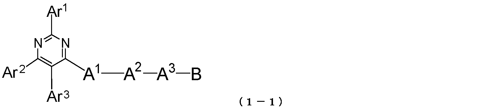
Ar1~Ar3、A1~A3及びBは、前記一般式(1)に記載した通
りの意味である、
2)前記ピリミジン誘導体が、下記一般式(1-2)で表されること、

Ar1~Ar3、A1~A3及びBは、前記一般式(1)に記載した通
りの意味である、
3)A1またはA2が、フェニレン基であること、
4)A1およびA2が、フェニレン基であること、
5)A1またはA2が、ナフチレン基であること、
6)Bが、ピリジル基、ビピリジル基、ターピリジル基、ピリミジニル基、ピラジニル基、トリアジニル基、ピロリル基、ピラゾリル基、イミダゾリル基、フリル基、チエニル基、キノリル基、イソキノリル基、キノキサリニル基、キナゾリニル基、ナフチリジニル基、インドリル基、ベンゾイミダゾリル基、ベンゾトリアゾリル基、ベンゾフラニル基、ベンゾチエニル基、ベンゾオキサゾリル基、ベンゾチアゾリル基、ベンゾチアジアゾリル基、ピリドピロリル基、ピリドイミダゾリル基、ピリドトリアゾリル基、アクリジニル基、フェナジニル基、フェナントロリニル基、フェノキサジニル基、フェノチアジニル基、カルバゾリル基、カルボリニル基、ジベンゾフラニル基またはジベンゾチエニル基であること、
7)Ar2がフェニル基であること、
8)Ar2が縮合多環芳香族基であり、特にナフチル基またはフェナントレニル基であること、
9)Ar3が水素原子であること、
10)Ar1がフェニル基であり、該フェニル基が置換基を有していること、特に、該フェニル基が有する置換基が縮合多環芳香族基であり、該縮合多環芳香族基は置換基を有していないこと、
11)Ar1が縮合多環芳香族基であり、特に、置換基を有していない縮合多環芳香族基であること、
が好ましい。
前記少なくとも一層の有機層が、前記ピリミジン誘導体を含んでいることを特徴とする有機EL素子が提供される。
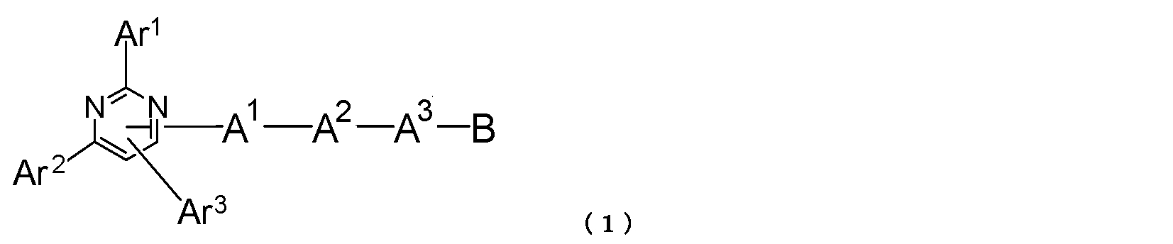

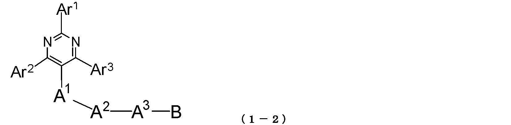
Ar1、Ar2は、それぞれ、芳香族炭化水素基または縮合多環芳香
族基を表す。
Ar3は、水素原子、芳香族炭化水素基または縮合多環芳香族基を表
す。
A1、A2は、芳香族炭化水素の2価基または縮合多環芳香族の2価
基を表す。
A3は、芳香族炭化水素の2価基、縮合多環芳香族の2価基または単
結合を表す。
Bは、芳香族複素環基を表す。
Ar1~Ar3で表される芳香族炭化水素基または縮合多環芳香族基としては、具体的に、フェニル基、ビフェニリル基、ターフェニリル基、テトラキスフェニル基、スチリル基、ナフチル基、アントラセニル基、アセナフテニル基、フェナントレニル基、フルオレニル基、インデニル基、ピレニル基、ペリレニル基、フルオランテニル基、トリフェニレニル基、スピロビフルオレニル基などをあげることができる。
ハロゲン原子、例えばフッ素原子、塩素原子、臭素原子、ヨウ素原子;
炭素原子数1~6のアルキル基、例えばメチル基、エチル基、n-プロ
ピル基、イソプロピル基、n-ブチル基、イソブチル基、tert-ブチ
ル基、n-ペンチル基、イソペンチル基、ネオペンチル基、n-ヘキシル
基;
炭素原子数1~6のアルキルオキシ基、例えばメチルオキシ基、エチル
オキシ基、プロピルオキシ基;
アルケニル基、例えばビニル基、アリル基;
アリールオキシ基、例えばフェニルオキシ基、トリルオキシ基;
アリールアルキルオキシ基、例えばベンジルオキシ基、フェネチルオキ
シ基;
芳香族炭化水素基または縮合多環芳香族基、例えばフェニル基、ビフェ
ニリル基、ターフェニリル基、ナフチル基、アントラセニル基、フェナン
トレニル基、フルオレニル基、インデニル基、ピレニル基、ペリレニル基
、フルオランテニル基、トリフェニレニル基、スピロビフルオレニル基、
アセナフテニル基;
芳香族複素環基、例えばピリジル基、フラニル基、チエニル基、フリル
基、ピロリル基、キノリル基、イソキノリル基、ベンゾフラニル基、ベン
ゾチエニル基、インドリル基、カルバゾリル基、ベンゾオキサゾリル基、
ベンゾチアゾリル基、キノキサリル基、ベンゾイミダゾリル基、ピラゾリ
ル基、ジベンゾフラニル基、ジベンゾチエニル基、カルボリニル基;
アリールビニル基、例えばスチリル基、ナフチルビニル基;
アシル基、例えばアセチル基、ベンゾイル基;
尚、炭素原子数1~6のアルキル基、アルケニル基、炭素原子数1~6のアルキルオキシ基は、直鎖状でも分枝状でもよい。これらの置換基は無置換でもよいが、さらに前記例示した置換基で置換されていても良い。また、これらの置換基同士は、独立して存在して環を形成していなくてもよいが、単結合、置換もしくは無置換のメチレン基、酸素原子または硫黄原子を介して互いに結合して環を形成していてもよい。
A1~A3で表される芳香族炭化水素の2価基または縮合多環芳香族の2価基は、芳香族炭化水素または縮合多環芳香族から水素原子を2個取り除いてできる。この場合の芳香族炭化水素または縮合多環芳香族としては、具体的に、ベンゼン、ビフェニル、ターフェニル、テトラキスフェニル、スチレン、ナフタレン、アントラセン、アセナフタレン、フルオレン、フェナントレン、インダン、ピレン、トリフェニレンなどをあげることができる。
Bで表される芳香族複素環基としては、具体的に、トリアジニル基、ピリジル基、ピリミジニル基、フリル基、ピロリル基、チエニル基、キノリル基、イソキノリル基、ベンゾフラニル基、ベンゾチエニル基、インドリル基、カルバゾリル基、ベンゾオキサゾリル基、ベンゾチアゾリル基、キノキサリニル基、ベンゾイミダゾリル基、ピラゾリル基、ジベンゾフラニル基、ジベンゾチエニル基、ナフチリジニル基、フェナントロリニル基、アクリジニル基、カルボリニル基、ビピリジル基、ターピリジル基、ピラジニル基、イミダゾリル基、キナゾリニル基、ベンゾトリアゾリル基、ベンゾチアジアゾリル基、ピリドピロリル基、ピリドイミダゾリル基、ピリドトリアゾリル基、フェナジニル基、フェノキサジニル基、フェノチアジニル基のような基をあげることができる。
本発明のピリミジン誘導体は公知の方法により製造することができ、例えば、以下のように合成できる。2,4,6-トリクロロピリミジンと、基Ar2に相当する基を有する、アリールボロン酸もしくはアリールボロン酸エステルとの鈴木カップリング反応を行って基Ar2に相当するアリール基で4位が置換されたピリミジン(以下、4位置換ピリミジンと呼ぶ。)を合成し、引き続き、かかる4位置換ピリミジンと、基A1-A2-A3-Bに相当する基を有する、ヘテロアリール基を置換基として有するアリールボロン酸もしくはアリールボロン酸エステルとの鈴木カップリング反応を行う。これによって、基A1-A2-A3-Bに相当する、ヘテロアリール基を置換基として有するアリール基がピリミジン環の6位に導入される。かくして得られたピリミジンを4位6位置換ピリミジンと呼ぶ。その後、4位6位置換ピリミジンと、Ar1に相当する基を有する、アリールボロン酸もしくはアリールボロン酸エステルとの鈴木カップリング反応を行う。これによって、本発明のピリミジン誘導体を合成することができる。
ここで、ハロゲン原子(例えばクロル基)の置換位置の異なるトリハロゲン化ピリミジンを用いると、置換位置の異なる本発明のピリミジン誘導体を合成することができる。
また、モノハロゲン化ピリミジンもしくはジハロゲン化ピリミジンを用い、同様にしてアリール基または/およびヘテロアリール基を置換基として有するアリール基を導入した後、N-ブロモコハク酸イミドなどによるハロゲン化を行うことによって、ピリミジン環にハロゲン基を導入し、続いて鈴木カップリング反応を行うことによって、アリール基または/およびヘテロアリール基を置換基として有するアリール基を導入し、置換位置の種々異なる本発明のピリミジン誘導体を合成することもできる。
本発明のピリミジン誘導体は、有機EL素子中の有機層の材料として好適である。本発明のピリミジン誘導体を使用して形成される有機EL素子(以下、本発明の有機EL素子と呼ぶことがある。)は、例えば、ガラス基板や透明プラスチック基板(例えばポリエチレンテレフタレート基板)などの基板上に順次、陽極、正孔輸送層、発光層、電子輸送層、陰極が形成された構成を有する。
陽極2としては、ITOや金のような仕事関数の大きな電極材料が用いられる。
正孔注入層3は、陽極2と正孔輸送層4との間に設けられる。正孔注入層3には、公知の材料、例えば、銅フタロシアニンに代表されるポルフィリン化合物;スターバースト型のトリフェニルアミン誘導体;トリフェニルアミン3量体および4量体、例えば分子中にトリフェニルアミン構造を3個以上有するアリールアミン化合物であって、トリフェニルアミン構造同士が単結合またはヘテロ原子を含まない2価基で連結しているアリールアミン化合物;アクセプター性の複素環化合物、例えばヘキサシアノアザトリフェニレン;塗布型の高分子材料;などを用いることができる。
正孔輸送層4は、上記の陽極2と発光層5の間に設けられるものである。正孔輸送層4には、例えば下記材料を用いることができる。
ベンジジン誘導体、例えば
N,N’-ジフェニル-N,N’-ジ(m-トリル)-ベンジジン
(TPD)、
N,N’-ジフェニル-N,N’-ジ(α-ナフチル)-ベンジジン
(NPD)、
N,N,N’,N’-テトラビフェニリルベンジジン;
1,1-ビス[(ジ-4-トリルアミノ)フェニル]シクロヘキサン(
TAPC);
種々のトリフェニルアミン3量体および4量体;
これらの材料は、単独で成膜に供してもよいが、複数の材料を混合して成膜に供してもよい。また、正孔輸送層4は、単層構造でも複数層の構造でもよい。
図27には示されていないが、正孔輸送層4と発光層5との間には、電子阻止層を設けることができる。電子阻止層には、電子阻止作用を有する公知の化合物を用いることができる。公知の化合物としては、以下を例示することができる。
カルバゾール誘導体、例えば
4,4’,4’’-トリ(N-カルバゾリル)トリフェニルアミン(
TCTA)、
9,9-ビス[4-(カルバゾール-9-イル)フェニル]フルオレ
ン、
1,3-ビス(カルバゾール-9-イル)ベンゼン(mCP)、
2,2-ビス(4-カルバゾール-9-イルフェニル)アダマンタン
(Ad-Cz);
トリフェニルシリル基とトリアリールアミン構造を有する化合物、例え
ば
9-[4-(カルバゾール-9-イル)フェニル]-9-[4-(ト
リフェニルシリル)フェニル]-9H-フルオレン;
電子阻止性の高いモノアミン化合物;
種々のトリフェニルアミン2量体;
これらは、単独で成膜に供してもよいが、複数の材料を混合して成膜に供してもよい。また、電子阻止層は、単層構造でも複数層の構造でもよい。
発光層5には、本発明のピリミジン誘導体のほか公知の発光材料を用いることができる。公知の発光材料としては、Alq3をはじめとするキノリノール誘導体の金属錯体などの各種の金属錯体;アントラセン誘導体;ビススチリルベンゼン誘導体;ピレン誘導体;オキサゾール誘導体;ポリパラフェニレンビニレン誘導体;などが挙げられる。
カルバゾール誘導体、例えば4,4’-ジ(N-カルバゾリル)ビフェ
ニル(CBP)、TCTA、mCP;
インドール環を縮合環の部分構造として有する複素環化合物;
あるいは、以下の電子輸送性のホスト材料を用いることができる。
p-ビス(トリフェニルシリル)ベンゼン(UGH2);
2,2’,2’’-(1,3,5-フェニレン)-トリス(1-フ
ェニル-1H-ベンズイミダゾール)(TPBI);
このようなホスト材料を用いると、高性能の有機EL素子を作製することができる。
発光層5と電子輸送層7との間には、正孔阻止層6を設けることができる。正孔阻止層6には、本発明のピリミジン誘導体のほか公知の正孔阻止作用を有する化合物を用いることができる。公知の正孔阻止作用を有する化合物としては、バソクプロイン(BCP)などのフェナントロリン誘導体や、BAlqなどのキノリノール誘導体の金属錯体のほか、各種の希土類錯体、オキサゾール誘導体、トリアゾール誘導体、トリアジン誘導体などが挙げられる。
電子輸送層7には、本発明のピリミジン誘導体のほか、Alq3、BAlqをはじめとするキノリノール誘導体の金属錯体などの各種金属錯体;トリアゾール誘導体;トリアジン誘導体;オキサジアゾール誘導体;ピリジン誘導体;ベンズイミダゾール誘導体;チアジアゾール誘導体;アントラセン誘導体;カルボジイミド誘導体;キノキサリン誘導体;ピリドインドール誘導体;フェナントロリン誘導体;シロール誘導体などを用いることができる。
電子注入層8は、電子輸送層7と陰極9の間に形成される。電子注入層8には、本発明のピリミジン誘導体のほか、フッ化リチウム、フッ化セシウムなどのアルカリ金属塩;フッ化マグネシウムなどのアルカリ土類金属塩;リチウムキノリノールなどのキノリノール誘導体の金属錯体;酸化アルミニウムなどの金属酸化物;などを用いることができるが、電子輸送層と陰極の好ましい選択においては、これを省略することができる。
陰極9では、アルミニウムのような仕事関数の低い電極材料や、マグネシウム銀合金、マグネシウムインジウム合金、アルミニウムマグネシウム合金のような仕事関数のより低い合金が電極材料として用いられる。
2-(ビフェニル-4-イル)-4-フェニル-6-{4’-(ピリジン-3-イル)ビフェニル-4-イル}ピリミジンの合成;
窒素置換した反応容器に、
2-クロロ-4-フェニル-6-{4’-(ピリジン-3-イル)ビ
フェニル-4-イル}ピリミジン 8.0g、
4-ビフェニルボロン酸 3.8g、
テトラキストリフェニルホスフィン 0.44g、
炭酸カリウム 7.9g、
トルエン 80ml、
テトラヒドロフラン 80mlおよび
水 40ml
を加えて加熱し、80℃で12時間撹拌して、反応液を調整した。反応液を室温まで冷却し、分液操作によって有機層を採取した。その後、減圧下濃縮することによって粗製物を得た。粗製物をカラムクロマトグラフ(担体:シリカゲル、溶離液:酢酸エチル/ヘプタン)で精製し、次いで、テトラヒドロフラン/アセトンの混合溶媒を用いた再結晶により精製した。その結果、2-(ビフェニル-4-イル)-4-フェニル-6-{4’-(ピリジン-3-イル)ビフェニル-4-イル}ピリミジン(化合物1)の白色粉体3.0g(収率30%)を得た。
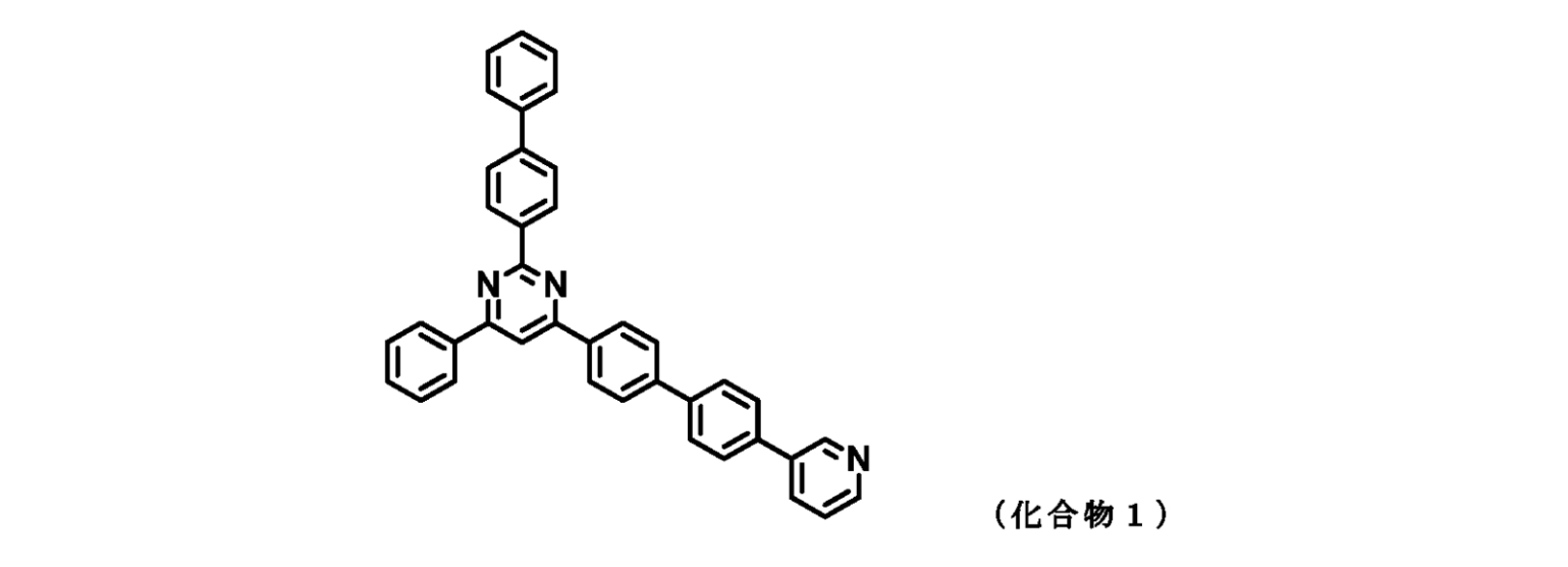
δ(ppm)=8.94(1H)
8.83(2H)
8.64(1H)
8.43-8.32(4H)
8.07(1H)
7.97-7.35(18H)
2-{4-(ナフタレン-1-イル)フェニル}-4-フェニル-6-{4’-(ピリジン-3-イル)ビフェニル-4-イル}ピリミジンの合成;
実施例1において、
4-ビフェニルボロン酸
に代えて
{4-(ナフタレン-1-イル)フェニル}ボロン酸
を用い、同様の条件で反応を行った。その結果、2-{4-(ナフタレン-1-イル)フェニル}-4-フェニル-6-{4’-(ピリジン-3-イル)ビフェニル-4-イル}ピリミジン(化合物2)の白色粉体1.6g(収率15%)を得た。

δ(ppm)=9.00-8.81(3H)
8.65(1H)
8.51-8.28(4H)
8.11-7.32(21H)
2,4-ビス(フェナンスレン-9-イル)-6-{4’-(ピリジン-3-イル)ビフェニル-4-イル}ピリミジンの合成;
実施例1において、
2-クロロ-4-フェニル-6-{4’-(ピリジン-3-イル)ビ
フェニル-4-イル}ピリミジン
に代えて
2-クロロ-4-(フェナンスレン-9-イル)-6-{4’-(ピ
リジン-3-イル)ビフェニル-4-イル}ピリミジン
を用い、
4-ビフェニルボロン酸
に代えて
フェナンスレン-9-ボロン酸
を用い、同様の条件で反応を行った。その結果、2,4-ビス(フェナンスレン-9-イル)-6-{4’-(ピリジン-3-イル)-ビフェニル-4-イル}ピリミジン(化合物29)の白色粉体1.2g(収率14%)を得た。
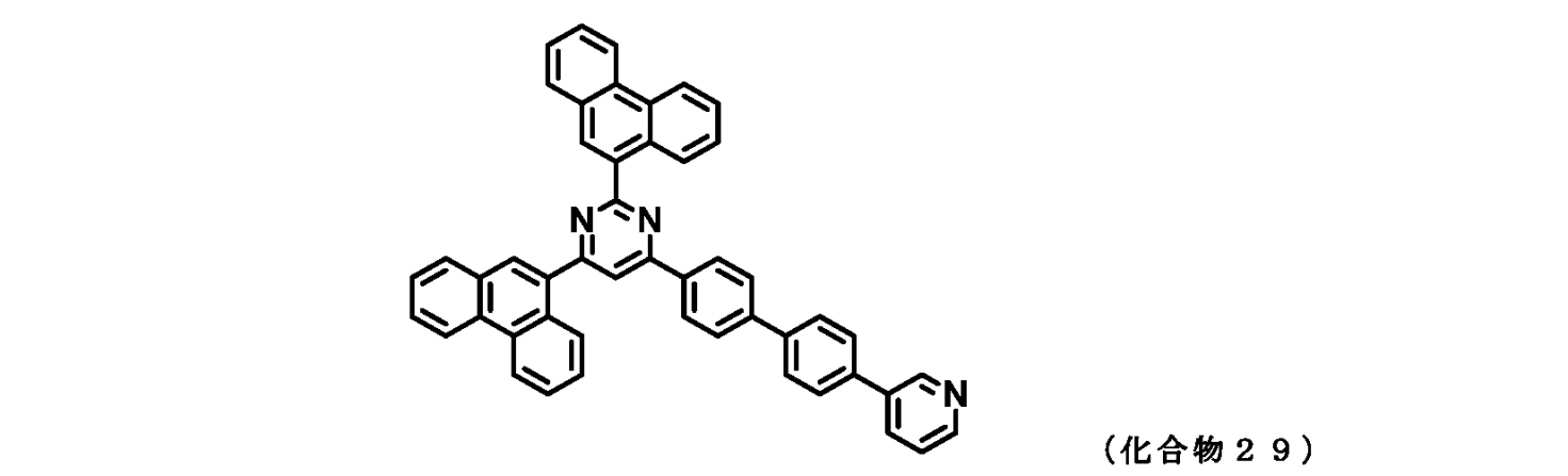
δ(ppm)=9.05-8.35(14H)
8.25-7.52(15H)
7.45-7.35(2H)
4-(ナフタレン-1-イル)-2-{4-(ナフタレン-1-イル)フェニル}-6-{4’-(ピリジン-3-イル)ビフェニル-4-イル}ピリミジンの合成;
実施例1において、
2-クロロ-4-フェニル-6-{4’-(ピリジン-3-イル)ビ
フェニル-4-イル}ピリミジン
に代えて
2-クロロ-4-(ナフタレン-1-イル)-6-{4’-(ピリジ
ン-3-イル)ビフェニル-4-イル}ピリミジン
を用い、
4-ビフェニルボロン酸
に代えて
4-(ナフタレン-1-イル)フェニルボロン酸
を用い、同様の条件で反応を行った。その結果、4-(ナフタレン-1-イル)-2-{4-(ナフタレン-1-イル)フェニル}-6-{4’-(ピリジン-3-イル)ビフェニル-4-イル}ピリミジン(化合物96)の白色粉体1.9g(収率28%)を得た。
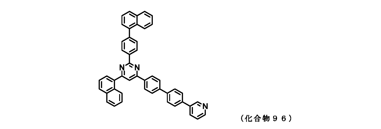
δ(ppm)=8.97(1H)
8.89(2H)
8.63(1H)
8.51-8.40(3H)
8.10-7.81(12H)
7.79-7.40(12H)
4-(ナフタレン-1-イル)-2-{4-(ナフタレン-2-イル)フェニル}-6-{4’-(ピリジン-3-イル)ビフェニル-4-イル}ピリミジンの合成;
実施例1において、
2-クロロ-4-フェニル-6-{4’-(ピリジン-3-イル)ビ
フェニル-4-イル}ピリミジン
に代えて
2-クロロ-4-(ナフタレン-1-イル)-6-{4’-(ピリジ
ン-3-イル)ビフェニル-4-イル}ピリミジン
を用い、
4-ビフェニルボロン酸
に代えて
4-(ナフタレン-2-イル)フェニルボロン酸
を用い、同様の条件で反応を行った。その結果、4-(ナフタレン-1-イル)-2-{4-(ナフタレン-2-イル)フェニル}-6-{4’-(ピリジン-3-イル)ビフェニル-4-イル}ピリミジン(化合物98)の白色粉体1.8g(収率26%)を得た。
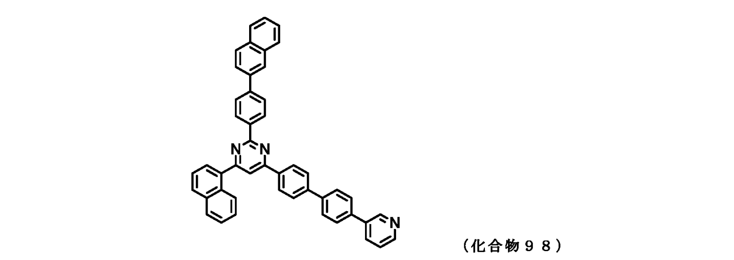
δ(ppm)=8.97(1H)
8.87(2H)
8.66(1H)
8.50-8.40(3H)
8.19(1H)
8.09-7.83(15H)
7.76(2H)
7.69(1H)
7.65-7.50(4H)
7.42(1H)
4-(ナフタレン-2-イル)-2-{4-(フェナンスレン-9-イル)フェニル}-6-{4’-(ピリジン-3-イル)ビフェニル-4-イル}ピリミジンの合成;
実施例1において、
2-クロロ-4-フェニル-6-{4’-(ピリジン-3-イル)ビ
フェニル-4-イル}ピリミジン
に代えて
2-クロロ-4-(ナフタレン-2-イル)-6-{4’-(ピリジ
ン-3-イル)ビフェニル-4-イル}ピリミジン
を用い、
4-ビフェニルボロン酸
に代えて
4-(フェナンスレン-9-イル)フェニルボロン酸
を用い、同様の条件で反応を行った。その結果、4-(ナフタレン-2-イル)-2-{4-(フェナンスレン-9-イル)フェニル}-6-{4’-(ピリジン-3-イル)ビフェニル-4-イル}ピリミジン(化合物100)の白色粉体1.5g(収率21%)を得た。

2-(ビフェニル-3-イル)-4-(9,9-ジメチルフルオレン-2-イル)-6-{4’-(ピリジン-3-イル)ビフェニル-4-イル}ピリミジンの合成;
実施例1において、
2-クロロ-4-フェニル-6-{4’-(ピリジン-3-イル)ビ
フェニル-4-イル}ピリミジン
に代えて
2-クロロ-4-(9,9-ジメチルフルオレン-2-イル)-6-
{4’-(ピリジン-3-イル)ビフェニル-4-イル}ピリミジン
を用い、
4-ビフェニルボロン酸
に代えて
3-ビフェニルボロン酸
を用い、同様の条件で反応を行った。その結果、2-(ビフェニル-3-イル)-4-(9,9-ジメチルフルオレン-2-イル)-6-{4’-(ピリジン-3-イル)ビフェニル-4-イル}ピリミジン(化合物104)の白色粉体1.8g(収率23%)を得た。

δ(ppm)=9.05(1H)
8.97(1H)
8.78(1H)
8.67(1H)
8.51-8.43(2H)
8.41-8.32(2H)
8.17(1H)
8.00-7.66(13H)
7.59-7.50(3H)
7.49-7.40(4H)
1.67(6H)
4-(ビフェニル-4-イル)-2-(フェナンスレン-9-イル)-6-{4’-(ピリジン-3-イル)ビフェニル-4-イル}ピリミジンの合成;
実施例1において、
2-クロロ-4-フェニル-6-{4’-(ピリジン-3-イル)ビ
フェニル-4-イル}ピリミジン
に代えて
2-クロロ-4-(ビフェニル-4-イル)-6-{4’-(ピリジ
ン-3-イル)ビフェニル-4-イル}ピリミジン
を用い、
4-ビフェニルボロン酸
に代えて
9-フェナンスレンボロン酸
を用い、同様の条件で反応を行った。その結果、4-(ビフェニル-4-イル)-2-(フェナンスレン-9-イル)-6-{4’-(ピリジン-3-イル)ビフェニル-4-イル}ピリミジン(化合物107)の黄白色粉体2.0g(収率30%)を得た。
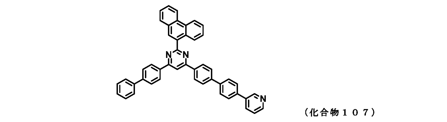
δ(ppm)=8.98(1H)
8.95-8.82(2H)
8.80(1H)
8.65(1H)
8.58(1H)
8.49-8.41(4H)
8.29(1H)
8.09(1H)
7.98(1H)
7.90-7.62(14H)
7.52(2H)
7.42(2H)
本発明の化合物を用いて、ITO基板の上に膜厚100nmの蒸着膜を作製して、イオン化ポテンシャル測定装置(住友重機械工業株式会社製、PYS-202型)で仕事関数を測定した。
仕事関数
実施例1の化合物(化合物1) 6.61V
実施例2の化合物(化合物2) 6.56V
実施例3の化合物(化合物29) 6.49V
実施例4の化合物(化合物96) 6.56V
実施例5の化合物(化合物98) 6.56V
実施例6の化合物(化合物100) 6.56V
実施例7の化合物(化合物104) 6.58V
実施例8の化合物(化合物107) 6.53V
各実施例で得られた化合物について、高感度示差走査熱量計(ブルカー・エイエックスエス製、DSC3100SA)によりガラス転移点を求めた。
ガラス転移点
実施例1の化合物(化合物1) 観測されず
実施例2の化合物(化合物2) 104℃
実施例3の化合物(化合物29) 137℃
実施例4の化合物(化合物96) 115℃
実施例5の化合物(化合物98) 112℃
実施例6の化合物(化合物100) 134℃
実施例7の化合物(化合物104) 110℃
実施例8の化合物(化合物107) 124℃
ガラス基板1上に透明陽極2としてITO電極をあらかじめ形成したものの上に、正孔注入層3、正孔輸送層4、発光層5、正孔阻止層6兼電子輸送層7、電子注入層8、陰極(アルミニウム電極)9の順に蒸着して、有機EL素子を作製した。
続いて、正孔注入層3を形成した。具体的には、透明陽極2を覆うように、下記構造式の化合物HIM-1を蒸着し、膜厚5nmの正孔注入層3を形成した。


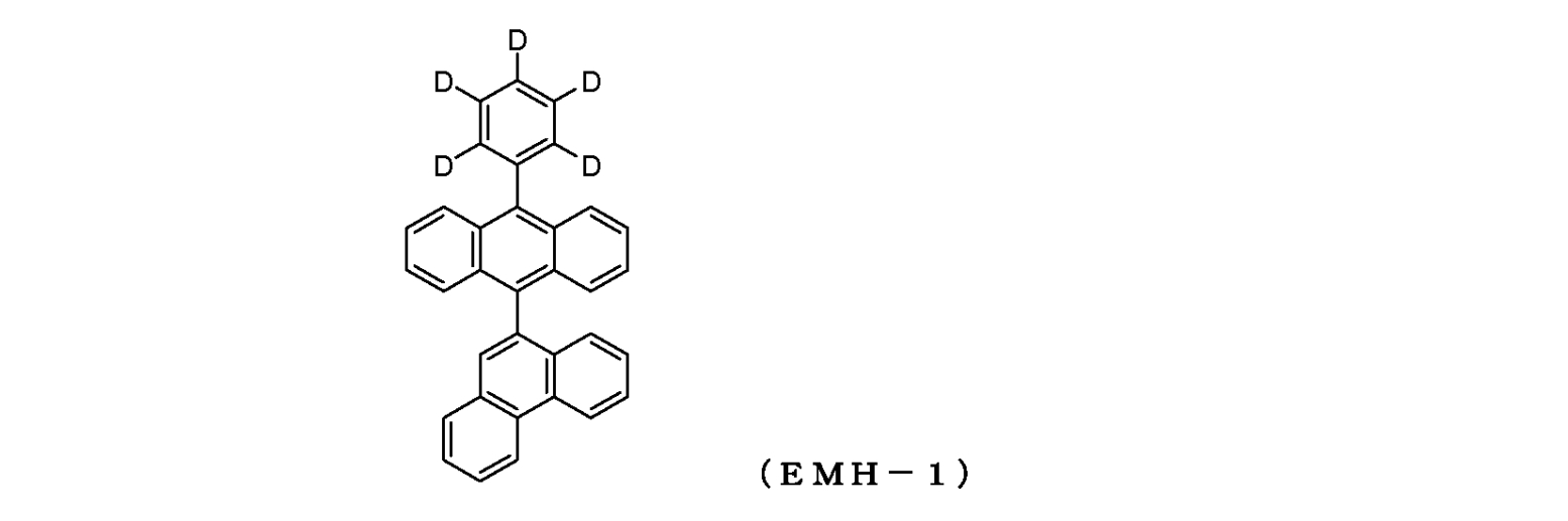
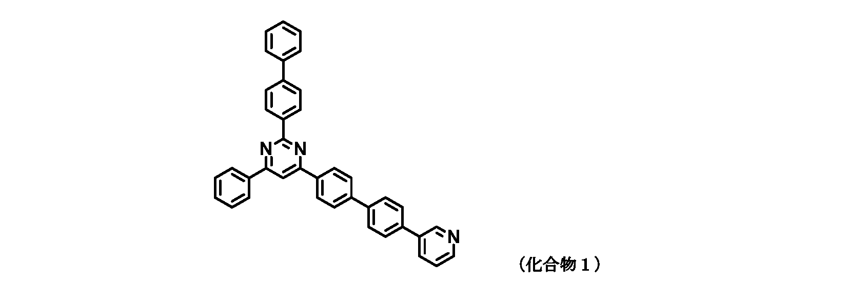

最後に、アルミニウムを100nm蒸着して陰極9を形成した。
作製した有機EL素子について、大気中、常温で直流電圧を印加したときの発光特性を測定した。結果を表1に示した。
素子実施例1において、正孔阻止層6兼電子輸送層7の材料として実施例1の化合物(化合物1)に代えて実施例2の化合物(化合物2)を用いた以外は、同様の条件で有機EL素子を作製した。作製した有機EL素子について、大気中、常温で直流電圧を印加したときの発光特性を測定した。結果を表1に示した。

素子実施例1において、正孔阻止層6兼電子輸送層7の材料として実施例1の化合物(化合物1)に代えて実施例3の化合物(化合物29)を用いた以外は、同様の条件で有機EL素子を作製した。作製した有機EL素子について、大気中、常温で直流電圧を印加したときの発光特性を測定した。結果を表1に示した。

素子実施例1において、正孔阻止層6兼電子輸送層7の材料として実施例1の化合物(化合物1)に代えて実施例4の化合物(化合物96)を用いた以外は、同様の条件で有機EL素子を作製した。作製した有機EL素子について、大気中、常温で直流電圧を印加したときの発光特性を測定した。結果を表1に示した。

素子実施例1において、正孔阻止層6兼電子輸送層7の材料として実施例1の化合物(化合物1)に代えて実施例5の化合物(化合物98)を用いた以外は、同様の条件で有機EL素子を作製した。作製した有機EL素子について、大気中、常温で直流電圧を印加したときの発光特性を測定した。結果を表1に示した。
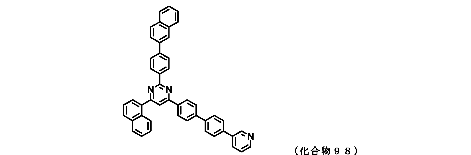
素子実施例1において、正孔阻止層6兼電子輸送層7の材料として実施例1の化合物(化合物1)に代えて実施例6の化合物(化合物100)を用いた以外は、同様の条件で有機EL素子を作製した。作製した有機EL素子について、大気中、常温で直流電圧を印加したときの発光特性を測定した。結果を表1に示した。
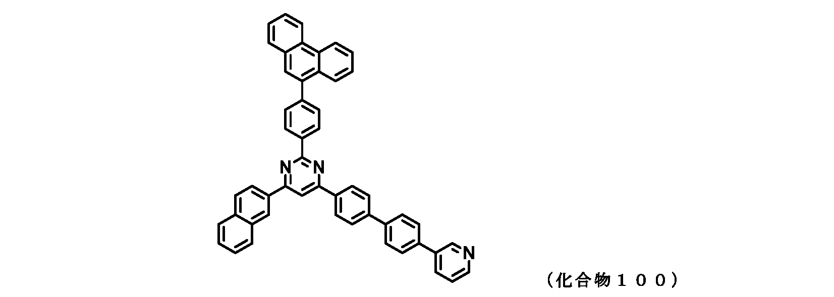
素子実施例1において、正孔阻止層6兼電子輸送層7の材料として実施例1の化合物(化合物1)に代えて実施例7の化合物(化合物104)を用いた以外は、同様の条件で有機EL素子を作製した。作製した有機EL素子について、大気中、常温で直流電圧を印加したときの発光特性を測定した。結果を表1に示した。

素子実施例1において、正孔阻止層6兼電子輸送層7の材料として実施例1の化合物(化合物1)に代えて実施例8の化合物(化合物107)を用いた以外は、同様の条件で有機EL素子を作製した。作製した有機EL素子について、大気中、常温で直流電圧を印加したときの発光特性を測定した。結果を表1に示した。

素子実施例1において、正孔阻止層6兼電子輸送層7の材料として実施例1の化合物(化合物1)に代えて下記構造式の化合物ETM-2(特許文献2参照)を用いた以外は、同様の条件で有機EL素子を作製した。作製した有機EL素子について、大気中、常温で直流電圧を印加したときの発光特性を測定した。結果を表1に示した。
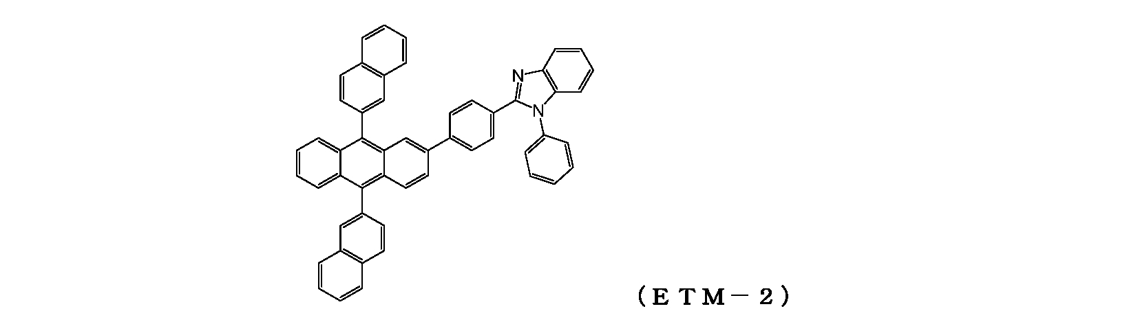

2 透明陽極
3 正孔注入層
4 正孔輸送層
5 発光層
6 正孔阻止層
7 電子輸送層
8 電子注入層
9 陰極
Claims (21)
- 下記一般式(1)で表されるピリミジン誘導体。

Ar1、Ar2は、それぞれ、芳香族炭化水素基または縮合多
環芳香族基を表し、
Ar3は、水素原子、芳香族炭化水素基または縮合多環芳香族
基を表し、
A1、A2は、芳香族炭化水素の2価基または縮合多環芳香族
の2価基を表し、
A3は、芳香族炭化水素の2価基、縮合多環芳香族の2価基ま
たは単結合を表し、
Bは、芳香族複素環基を表す。 - 下記一般式(1-1)で表される、請求項1記載のピリミジン誘導体。

Ar1~Ar3、A1~A3及びBは、前記一般式(1)に記載
した通りの意味である。 - 下記一般式(1-2)で表される、請求項1記載のピリミジン誘導体。

Ar1~Ar3、A1~A3及びBは、前記一般式(1)に記載
した通りの意味である。 - A1またはA2がフェニレン基である、請求項1記載のピリミジン誘導体。
- A1およびA2がフェニレン基である、請求項1記載のピリミジン誘導体。
- A1またはA2がナフチレン基である、請求項1記載のピリミジン誘導体。
- Bが、ピリジル基、ビピリジル基、ターピリジル基、ピリミジニル基、ピラジニル基、トリアジニル基、ピロリル基、ピラゾリル基、イミダゾリル基、フリル基、チエニル基、キノリル基、イソキノリル基、キノキサリニル基、キナゾリニル基、ナフチリジニル基、インドリル基、ベンゾイミダゾリル基、ベンゾトリアゾリル基、ベンゾフラニル基、ベンゾチエニル基、ベンゾオキサゾリル基、ベンゾチアゾリル基、ベンゾチアジアゾリル基、ピリドピロリル基、ピリドイミダゾリル基、ピリドトリアゾリル基、アクリジニル基、フェナジニル基、フェナントロリニル基、フェノキサジニル基、フェノチアジニル基、カルバゾリル基、カルボリニル基、ジベンゾフラニル基またはジベンゾチエニル基である、請求項1記載のピリミジン誘導体。
- Ar2がフェニル基である、請求項1記載のピリミジン誘導体。
- Ar2が縮合多環芳香族基である、請求項1記載のピリミジン誘導体。
- 前記縮合多環芳香族基がナフチル基である、請求項9記載のピリミジン誘導体。
- 前記縮合多環芳香族基がフェナントレニル基である、請求項9記載のピリミジン誘導体。
- Ar3が水素原子である、請求項1記載のピリミジン誘導体。
- Ar1がフェニル基であり、該フェニル基が置換基を有している、請求項1記載のピリミジン誘導体。
- 前記フェニル基が有する置換基が縮合多環芳香族基であり、該縮合多環芳香族基は置換基を有していない、請求項13記載のピリミジン誘導体。
- Ar1が縮合多環芳香族基である、請求項1記載のピリミジン誘導体。
- 前記縮合多環芳香族基が置換基を有していない、請求項15記載のピリミジン誘導体。
- 一対の電極とその間に挟まれた少なくとも一層の有機層を有する有機エレクトロルミネッセンス素子において、
前記少なくとも一層の有機層が、請求項1記載のピリミジン誘導体を含んでいることを特徴とする有機エレクトロルミネッセンス素子。 - 前記ピリミジン誘導体を含んでいる有機層が電子輸送層である、請求項17記載の有機エレクトロルミネッセンス素子。
- 前記ピリミジン誘導体を含んでいる有機層が正孔阻止層である、請求項17記載の有機エレクトロルミネッセンス素子。
- 前記ピリミジン誘導体を含んでいる有機層が発光層である、請求項17記載の有機エレクトロルミネッセンス素子。
- 前記ピリミジン誘導体を含んでいる有機層が電子注入層である、請求項17記載の有機エレクトロルミネッセンス素子。
Priority Applications (5)
| Application Number | Priority Date | Filing Date | Title |
|---|---|---|---|
| KR1020177023112A KR102495161B1 (ko) | 2015-01-20 | 2016-01-13 | 피리미딘 유도체 및 유기 전계발광 소자 |
| JP2016570588A JP6731355B2 (ja) | 2015-01-20 | 2016-01-13 | ピリミジン誘導体および有機エレクトロルミネッセンス素子 |
| US15/544,116 US10566543B2 (en) | 2015-01-20 | 2016-01-13 | Pyrimidine derivative and organic electroluminescent devices |
| CN201680016995.8A CN107406415B (zh) | 2015-01-20 | 2016-01-13 | 嘧啶衍生物和有机电致发光器件 |
| EP16740036.5A EP3248966B1 (en) | 2015-01-20 | 2016-01-13 | Pyrimidine derivatives and organic electroluminescent devices |
Applications Claiming Priority (2)
| Application Number | Priority Date | Filing Date | Title |
|---|---|---|---|
| JP2015-008229 | 2015-01-20 | ||
| JP2015008229 | 2015-01-20 |
Publications (1)
| Publication Number | Publication Date |
|---|---|
| WO2016117429A1 true WO2016117429A1 (ja) | 2016-07-28 |
Family
ID=56416976
Family Applications (1)
| Application Number | Title | Priority Date | Filing Date |
|---|---|---|---|
| PCT/JP2016/050832 WO2016117429A1 (ja) | 2015-01-20 | 2016-01-13 | ピリミジン誘導体および有機エレクトロルミネッセンス素子 |
Country Status (7)
| Country | Link |
|---|---|
| US (1) | US10566543B2 (ja) |
| EP (1) | EP3248966B1 (ja) |
| JP (1) | JP6731355B2 (ja) |
| KR (1) | KR102495161B1 (ja) |
| CN (1) | CN107406415B (ja) |
| TW (1) | TWI733659B (ja) |
| WO (1) | WO2016117429A1 (ja) |
Cited By (2)
| Publication number | Priority date | Publication date | Assignee | Title |
|---|---|---|---|---|
| JP2017175099A (ja) * | 2016-03-25 | 2017-09-28 | ▲いく▼▲雷▼光電科技股▲分▼有限公司 | 有機エレクトロルミネセントデバイス用の化合物、およびこの化合物を用いた有機エレクトロルミネセントデバイス |
| JP2020509584A (ja) * | 2017-02-28 | 2020-03-26 | ローム・アンド・ハース・エレクトロニック・マテリアルズ・コリア・リミテッド | 有機エレクトロルミネッセンスデバイス |
Families Citing this family (5)
| Publication number | Priority date | Publication date | Assignee | Title |
|---|---|---|---|---|
| US11581487B2 (en) | 2017-04-26 | 2023-02-14 | Oti Lumionics Inc. | Patterned conductive coating for surface of an opto-electronic device |
| CN107827826A (zh) * | 2017-11-02 | 2018-03-23 | 上海道亦化工科技有限公司 | 一种嘧啶衍生物及其用途和有机电致发光器件 |
| US11751415B2 (en) | 2018-02-02 | 2023-09-05 | Oti Lumionics Inc. | Materials for forming a nucleation-inhibiting coating and devices incorporating same |
| CN109081830A (zh) * | 2018-07-13 | 2018-12-25 | 昱镭光电科技股份有限公司 | 经苯并咪唑取代之二苯基嘧啶化合物及其有机电致发光器件 |
| JP7390739B2 (ja) | 2019-03-07 | 2023-12-04 | オーティーアイ ルミオニクス インコーポレーテッド | 核生成抑制コーティングを形成するための材料およびそれを組み込んだデバイス |
Citations (18)
| Publication number | Priority date | Publication date | Assignee | Title |
|---|---|---|---|---|
| WO2005076669A1 (ja) * | 2004-02-09 | 2005-08-18 | Idemitsu Kosan Co., Ltd. | 有機エレクトロルミネッセンス素子 |
| WO2005085387A1 (ja) * | 2004-03-08 | 2005-09-15 | Idemitsu Kosan Co., Ltd. | 有機エレクトロルミネッセンス素子用材料及びそれを利用した有機エレクトロルミネッセンス素子 |
| WO2011005060A2 (ko) * | 2009-07-10 | 2011-01-13 | 제일모직 주식회사 | 유기광전소자용 화합물 및 이를 포함하는 유기광전소자 |
| WO2011013783A1 (ja) * | 2009-07-31 | 2011-02-03 | 富士フイルム株式会社 | 有機電界発光素子 |
| WO2011013830A1 (ja) * | 2009-07-31 | 2011-02-03 | 富士フイルム株式会社 | 有機電界発光素子 |
| JP2011049512A (ja) * | 2009-07-31 | 2011-03-10 | Fujifilm Corp | 有機電界発光素子 |
| WO2012005360A1 (ja) * | 2010-07-09 | 2012-01-12 | 富士フイルム株式会社 | 有機電界発光素子 |
| WO2013077362A1 (ja) * | 2011-11-22 | 2013-05-30 | 出光興産株式会社 | 芳香族複素環誘導体、有機エレクトロルミネッセンス素子用材料および有機エレクトロルミネッセンス素子 |
| KR20130060157A (ko) * | 2011-11-29 | 2013-06-07 | 에스에프씨 주식회사 | 안트라센 유도체 및 이를 포함하는 유기전계발광소자 |
| CN103396404A (zh) * | 2013-07-31 | 2013-11-20 | 华南理工大学 | 一种以三苯基嘧啶为核的化合物及其制备方法和应用 |
| WO2013175747A1 (ja) * | 2012-05-22 | 2013-11-28 | 出光興産株式会社 | 有機エレクトロルミネッセンス素子 |
| WO2013175746A1 (ja) * | 2012-05-22 | 2013-11-28 | 出光興産株式会社 | 有機エレクトロルミネッセンス素子 |
| WO2014010824A1 (ko) * | 2012-07-13 | 2014-01-16 | 주식회사 엘지화학 | 헤테로환 화합물 및 이를 포함하는 유기 전자 소자 |
| JP2014507383A (ja) * | 2010-12-13 | 2014-03-27 | ビーエーエスエフ ソシエタス・ヨーロピア | 電子装置用途のためのビスピリミジン |
| KR20140079306A (ko) * | 2012-12-18 | 2014-06-26 | 에스에프씨 주식회사 | 유기발광 화합물 및 이를 포함하는 유기전계발광소자 |
| CN103951657A (zh) * | 2014-05-09 | 2014-07-30 | 江西冠能光电材料有限公司 | 一种高电负性有机半导体 |
| WO2014209028A1 (ko) * | 2013-06-28 | 2014-12-31 | 주식회사 엘지화학 | 헤테로환 화합물 및 이를 포함하는 유기 발광 소자 |
| WO2014208775A1 (en) * | 2013-06-27 | 2014-12-31 | Ricoh Company, Ltd. | Electrochromic compound, electrochromic composition, display element, and dimming element |
Family Cites Families (20)
| Publication number | Priority date | Publication date | Assignee | Title |
|---|---|---|---|---|
| JP2734341B2 (ja) | 1993-03-26 | 1998-03-30 | 住友電気工業株式会社 | 有機エレクトロルミネッセンス素子 |
| EP0647694B1 (en) | 1993-03-26 | 1999-09-15 | Sumitomo Electric Industries, Ltd. | Organic electroluminescent elements |
| KR100691543B1 (ko) | 2002-01-18 | 2007-03-09 | 주식회사 엘지화학 | 새로운 전자 수송용 물질 및 이를 이용한 유기 발광 소자 |
| EP2770036B1 (en) * | 2002-03-15 | 2017-12-20 | Idemitsu Kosan Co., Ltd | Material for organic electroluminescent devices and organic electroluminescent devices made by using the same |
| WO2003080760A1 (fr) * | 2002-03-22 | 2003-10-02 | Idemitsu Kosan Co., Ltd. | Materiau pour dispositifs electroluminescents organiques et dispositifs electroluminescents organiques produits avec ce materiau |
| US8012602B2 (en) * | 2002-10-30 | 2011-09-06 | Basf Se | Electroluminescent device |
| US9923148B2 (en) * | 2002-10-30 | 2018-03-20 | Udc Ireland Limited | Electroluminescent device |
| KR20070030759A (ko) * | 2004-03-08 | 2007-03-16 | 이데미쓰 고산 가부시키가이샤 | 유기 전기 발광 소자용 재료 및 이를 이용한 유기 전기발광 소자 |
| KR101174090B1 (ko) * | 2008-08-25 | 2012-08-14 | 제일모직주식회사 | 유기광전소자용 재료 및 이를 포함하는 유기광전소자 |
| EP2468731B1 (en) * | 2009-08-21 | 2014-11-05 | Tosoh Corporation | Cyclic azine derivatives, processes for producing these, and organic electroluminescent element containing these as component |
| KR20120057606A (ko) * | 2010-03-05 | 2012-06-05 | 이데미쓰 고산 가부시키가이샤 | 유기 일렉트로루미네선스 소자용 재료 및 그것을 사용한 유기 일렉트로루미네선스 소자 |
| DE102010013806B4 (de) * | 2010-04-03 | 2021-06-10 | Merck Patent Gmbh | Materialien für organische Elektrolumineszenzvorrichtungen |
| US9324950B2 (en) * | 2010-11-22 | 2016-04-26 | Idemitsu Kosan Co., Ltd. | Organic electroluminescence device |
| WO2012070233A1 (en) * | 2010-11-22 | 2012-05-31 | Idemitsu Kosan Co.,Ltd. | Organic electroluminescence device |
| KR101478000B1 (ko) * | 2010-12-21 | 2015-01-05 | 롬엔드하스전자재료코리아유한회사 | 신규한 유기 발광 화합물 및 이를 채용하고 있는 유기 전계 발광 소자 |
| EP2752902B9 (en) * | 2011-11-22 | 2017-08-30 | Idemitsu Kosan Co., Ltd | Aromatic heterocyclic derivative, material for organic electroluminescent element, and organic electroluminescent element |
| JP6095391B2 (ja) * | 2013-02-06 | 2017-03-15 | キヤノン株式会社 | 有機発光素子 |
| TWI482759B (zh) * | 2013-02-07 | 2015-05-01 | Lg Chemical Ltd | 雜環化合物及使用其之有機發光裝置 |
| JP6317544B2 (ja) * | 2013-02-15 | 2018-04-25 | 出光興産株式会社 | 有機エレクトロルミネッセンス素子および電子機器 |
| KR101546788B1 (ko) * | 2013-12-27 | 2015-08-24 | 희성소재 (주) | 헤테로고리 화합물 및 이를 이용한 유기발광소자 |
-
2016
- 2016-01-13 WO PCT/JP2016/050832 patent/WO2016117429A1/ja active Application Filing
- 2016-01-13 KR KR1020177023112A patent/KR102495161B1/ko active IP Right Grant
- 2016-01-13 EP EP16740036.5A patent/EP3248966B1/en active Active
- 2016-01-13 US US15/544,116 patent/US10566543B2/en active Active
- 2016-01-13 CN CN201680016995.8A patent/CN107406415B/zh active Active
- 2016-01-13 JP JP2016570588A patent/JP6731355B2/ja active Active
- 2016-01-19 TW TW105101460A patent/TWI733659B/zh active
Patent Citations (19)
| Publication number | Priority date | Publication date | Assignee | Title |
|---|---|---|---|---|
| WO2005076669A1 (ja) * | 2004-02-09 | 2005-08-18 | Idemitsu Kosan Co., Ltd. | 有機エレクトロルミネッセンス素子 |
| WO2005085387A1 (ja) * | 2004-03-08 | 2005-09-15 | Idemitsu Kosan Co., Ltd. | 有機エレクトロルミネッセンス素子用材料及びそれを利用した有機エレクトロルミネッセンス素子 |
| WO2011005060A2 (ko) * | 2009-07-10 | 2011-01-13 | 제일모직 주식회사 | 유기광전소자용 화합물 및 이를 포함하는 유기광전소자 |
| WO2011013783A1 (ja) * | 2009-07-31 | 2011-02-03 | 富士フイルム株式会社 | 有機電界発光素子 |
| WO2011013830A1 (ja) * | 2009-07-31 | 2011-02-03 | 富士フイルム株式会社 | 有機電界発光素子 |
| JP2011049512A (ja) * | 2009-07-31 | 2011-03-10 | Fujifilm Corp | 有機電界発光素子 |
| WO2012005360A1 (ja) * | 2010-07-09 | 2012-01-12 | 富士フイルム株式会社 | 有機電界発光素子 |
| JP2014507383A (ja) * | 2010-12-13 | 2014-03-27 | ビーエーエスエフ ソシエタス・ヨーロピア | 電子装置用途のためのビスピリミジン |
| WO2013077362A1 (ja) * | 2011-11-22 | 2013-05-30 | 出光興産株式会社 | 芳香族複素環誘導体、有機エレクトロルミネッセンス素子用材料および有機エレクトロルミネッセンス素子 |
| KR20130060157A (ko) * | 2011-11-29 | 2013-06-07 | 에스에프씨 주식회사 | 안트라센 유도체 및 이를 포함하는 유기전계발광소자 |
| WO2013175747A1 (ja) * | 2012-05-22 | 2013-11-28 | 出光興産株式会社 | 有機エレクトロルミネッセンス素子 |
| WO2013175746A1 (ja) * | 2012-05-22 | 2013-11-28 | 出光興産株式会社 | 有機エレクトロルミネッセンス素子 |
| WO2014010824A1 (ko) * | 2012-07-13 | 2014-01-16 | 주식회사 엘지화학 | 헤테로환 화합물 및 이를 포함하는 유기 전자 소자 |
| KR20140079306A (ko) * | 2012-12-18 | 2014-06-26 | 에스에프씨 주식회사 | 유기발광 화합물 및 이를 포함하는 유기전계발광소자 |
| WO2014208775A1 (en) * | 2013-06-27 | 2014-12-31 | Ricoh Company, Ltd. | Electrochromic compound, electrochromic composition, display element, and dimming element |
| WO2014209028A1 (ko) * | 2013-06-28 | 2014-12-31 | 주식회사 엘지화학 | 헤테로환 화합물 및 이를 포함하는 유기 발광 소자 |
| WO2014208829A1 (ko) * | 2013-06-28 | 2014-12-31 | 주식회사 엘지화학 | 헤테로환 화합물 및 이를 포함하는 유기 발광 소자 |
| CN103396404A (zh) * | 2013-07-31 | 2013-11-20 | 华南理工大学 | 一种以三苯基嘧啶为核的化合物及其制备方法和应用 |
| CN103951657A (zh) * | 2014-05-09 | 2014-07-30 | 江西冠能光电材料有限公司 | 一种高电负性有机半导体 |
Non-Patent Citations (1)
| Title |
|---|
| See also references of EP3248966A4 * |
Cited By (2)
| Publication number | Priority date | Publication date | Assignee | Title |
|---|---|---|---|---|
| JP2017175099A (ja) * | 2016-03-25 | 2017-09-28 | ▲いく▼▲雷▼光電科技股▲分▼有限公司 | 有機エレクトロルミネセントデバイス用の化合物、およびこの化合物を用いた有機エレクトロルミネセントデバイス |
| JP2020509584A (ja) * | 2017-02-28 | 2020-03-26 | ローム・アンド・ハース・エレクトロニック・マテリアルズ・コリア・リミテッド | 有機エレクトロルミネッセンスデバイス |
Also Published As
| Publication number | Publication date |
|---|---|
| TWI733659B (zh) | 2021-07-21 |
| JPWO2016117429A1 (ja) | 2017-11-09 |
| KR20170103976A (ko) | 2017-09-13 |
| US20180006239A1 (en) | 2018-01-04 |
| EP3248966A4 (en) | 2018-06-20 |
| US10566543B2 (en) | 2020-02-18 |
| KR102495161B1 (ko) | 2023-02-01 |
| CN107406415A (zh) | 2017-11-28 |
| CN107406415B (zh) | 2021-02-19 |
| EP3248966A1 (en) | 2017-11-29 |
| EP3248966B1 (en) | 2022-12-21 |
| TW201634458A (zh) | 2016-10-01 |
| JP6731355B2 (ja) | 2020-07-29 |
Similar Documents
| Publication | Publication Date | Title |
|---|---|---|
| JP6501771B2 (ja) | ピリミジン誘導体および有機エレクトロルミネッセンス素子 | |
| JP5719308B2 (ja) | 置換されたアントラセン環構造とピリドインドール環構造を有する化合物および有機エレクトロルミネッセンス素子 | |
| WO2011105373A1 (ja) | 置換されたピリジル化合物および有機エレクトロルミネッセンス素子 | |
| JP6731355B2 (ja) | ピリミジン誘導体および有機エレクトロルミネッセンス素子 | |
| WO2014188947A1 (ja) | 新規なピリミジン誘導体および有機エレクトロルミネッセンス素子 | |
| JP5683763B1 (ja) | ベンゾピリドインドール誘導体および有機エレクトロルミネッセンス素子 | |
| TWI743146B (zh) | 具有苯并唑環結構之化合物及有機電致發光元件 | |
| JP7394050B2 (ja) | ベンゾイミダゾール環構造を有する化合物および有機エレクトロルミネッセンス素子 | |
| WO2012098849A1 (ja) | 置換されたビピリジル基とピリドインドール環構造を有する化合物および有機エレクトロルミネッセンス素子 | |
| WO2017051765A1 (ja) | 有機エレクトロルミネッセンス素子 | |
| JP6301729B2 (ja) | インドロキノキサリン環構造を有する化合物および有機エレクトロルミネッセンス素子 | |
| JP7369714B2 (ja) | アザベンゾオキサゾール環構造を有する化合物および有機エレクトロルミネッセンス素子 | |
| WO2012115219A1 (ja) | ビピリジル基とカルバゾール環を有する化合物及び有機エレクトロルミネッセンス素子 | |
| JP7406500B2 (ja) | ピリミジン環構造を有する化合物および有機エレクトロルミネッセンス素子 | |
| KR102603365B1 (ko) | 피리미딘 고리 구조를 갖는 화합물 및 유기 일렉트로 루미네선스 소자 | |
| WO2015125679A1 (ja) | ベンゾフロインドール誘導体および有機エレクトロルミネッセンス素子 | |
| JP6479770B2 (ja) | キノリノトリアゾール誘導体および有機エレクトロルミネッセンス素子 | |
| JPWO2019039402A1 (ja) | インデノベンゾアゾール環構造を有する化合物および有機エレクトロルミネッセンス素子 |
Legal Events
| Date | Code | Title | Description |
|---|---|---|---|
| 121 | Ep: the epo has been informed by wipo that ep was designated in this application |
Ref document number: 16740036 Country of ref document: EP Kind code of ref document: A1 |
|
| ENP | Entry into the national phase |
Ref document number: 2016570588 Country of ref document: JP Kind code of ref document: A |
|
| WWE | Wipo information: entry into national phase |
Ref document number: 15544116 Country of ref document: US |
|
| NENP | Non-entry into the national phase |
Ref country code: DE |
|
| REEP | Request for entry into the european phase |
Ref document number: 2016740036 Country of ref document: EP |
|
| ENP | Entry into the national phase |
Ref document number: 20177023112 Country of ref document: KR Kind code of ref document: A |