KR20180137606A - Semiconductor device and method for manufacturing the same - Google Patents
Semiconductor device and method for manufacturing the same Download PDFInfo
- Publication number
- KR20180137606A KR20180137606A KR1020187036791A KR20187036791A KR20180137606A KR 20180137606 A KR20180137606 A KR 20180137606A KR 1020187036791 A KR1020187036791 A KR 1020187036791A KR 20187036791 A KR20187036791 A KR 20187036791A KR 20180137606 A KR20180137606 A KR 20180137606A
- Authority
- KR
- South Korea
- Prior art keywords
- electrode
- transistor
- gate electrode
- layer
- gate
- Prior art date
Links
- 239000004065 semiconductor Substances 0.000 title claims abstract description 194
- 238000000034 method Methods 0.000 title claims description 74
- 238000004519 manufacturing process Methods 0.000 title abstract description 30
- 239000000463 material Substances 0.000 claims description 48
- 239000004973 liquid crystal related substance Substances 0.000 claims description 47
- 239000003990 capacitor Substances 0.000 claims description 29
- 239000010936 titanium Substances 0.000 claims description 24
- 229910052719 titanium Inorganic materials 0.000 claims description 15
- RTAQQCXQSZGOHL-UHFFFAOYSA-N Titanium Chemical compound [Ti] RTAQQCXQSZGOHL-UHFFFAOYSA-N 0.000 claims description 13
- 230000015572 biosynthetic process Effects 0.000 claims description 13
- 230000009977 dual effect Effects 0.000 claims description 12
- 229910052750 molybdenum Inorganic materials 0.000 claims description 12
- ZOKXTWBITQBERF-UHFFFAOYSA-N Molybdenum Chemical compound [Mo] ZOKXTWBITQBERF-UHFFFAOYSA-N 0.000 claims description 10
- 239000011733 molybdenum Substances 0.000 claims description 10
- 229910052733 gallium Inorganic materials 0.000 claims description 5
- GYHNNYVSQQEPJS-UHFFFAOYSA-N Gallium Chemical compound [Ga] GYHNNYVSQQEPJS-UHFFFAOYSA-N 0.000 claims description 2
- 229910052738 indium Inorganic materials 0.000 claims description 2
- APFVFJFRJDLVQX-UHFFFAOYSA-N indium atom Chemical compound [In] APFVFJFRJDLVQX-UHFFFAOYSA-N 0.000 claims description 2
- JBQYATWDVHIOAR-UHFFFAOYSA-N tellanylidenegermanium Chemical compound [Te]=[Ge] JBQYATWDVHIOAR-UHFFFAOYSA-N 0.000 claims 1
- 239000010409 thin film Substances 0.000 abstract description 157
- 239000000758 substrate Substances 0.000 abstract description 81
- 239000010410 layer Substances 0.000 description 337
- 239000010408 film Substances 0.000 description 187
- 229910007541 Zn O Inorganic materials 0.000 description 34
- 230000008569 process Effects 0.000 description 34
- 230000001681 protective effect Effects 0.000 description 34
- 238000004544 sputter deposition Methods 0.000 description 32
- 229910052782 aluminium Inorganic materials 0.000 description 27
- XAGFODPZIPBFFR-UHFFFAOYSA-N aluminium Chemical compound [Al] XAGFODPZIPBFFR-UHFFFAOYSA-N 0.000 description 25
- 230000006870 function Effects 0.000 description 21
- 238000010586 diagram Methods 0.000 description 19
- XKRFYHLGVUSROY-UHFFFAOYSA-N Argon Chemical compound [Ar] XKRFYHLGVUSROY-UHFFFAOYSA-N 0.000 description 18
- 239000011159 matrix material Substances 0.000 description 16
- 238000000206 photolithography Methods 0.000 description 16
- 102100040862 Dual specificity protein kinase CLK1 Human genes 0.000 description 14
- XLOMVQKBTHCTTD-UHFFFAOYSA-N Zinc monoxide Chemical compound [Zn]=O XLOMVQKBTHCTTD-UHFFFAOYSA-N 0.000 description 14
- 238000005530 etching Methods 0.000 description 14
- 239000000956 alloy Substances 0.000 description 13
- 239000013078 crystal Substances 0.000 description 13
- 229910045601 alloy Inorganic materials 0.000 description 12
- 239000012298 atmosphere Substances 0.000 description 12
- 230000001413 cellular effect Effects 0.000 description 12
- 239000011651 chromium Substances 0.000 description 11
- 239000010949 copper Substances 0.000 description 11
- 239000002356 single layer Substances 0.000 description 11
- 229910052581 Si3N4 Inorganic materials 0.000 description 10
- 239000004020 conductor Substances 0.000 description 10
- 229920005989 resin Polymers 0.000 description 10
- 239000011347 resin Substances 0.000 description 10
- HQVNEWCFYHHQES-UHFFFAOYSA-N silicon nitride Chemical compound N12[Si]34N5[Si]62N3[Si]51N64 HQVNEWCFYHHQES-UHFFFAOYSA-N 0.000 description 10
- 229910052786 argon Inorganic materials 0.000 description 9
- 238000004891 communication Methods 0.000 description 9
- 239000011521 glass Substances 0.000 description 9
- 238000010438 heat treatment Methods 0.000 description 9
- 239000000203 mixture Substances 0.000 description 9
- 238000003860 storage Methods 0.000 description 9
- 101000749294 Homo sapiens Dual specificity protein kinase CLK1 Proteins 0.000 description 8
- VYPSYNLAJGMNEJ-UHFFFAOYSA-N Silicium dioxide Chemical compound O=[Si]=O VYPSYNLAJGMNEJ-UHFFFAOYSA-N 0.000 description 8
- 239000007789 gas Substances 0.000 description 8
- 239000007769 metal material Substances 0.000 description 8
- 239000003566 sealing material Substances 0.000 description 8
- 229910052814 silicon oxide Inorganic materials 0.000 description 8
- 238000012360 testing method Methods 0.000 description 8
- RYGMFSIKBFXOCR-UHFFFAOYSA-N Copper Chemical compound [Cu] RYGMFSIKBFXOCR-UHFFFAOYSA-N 0.000 description 7
- 229910052779 Neodymium Inorganic materials 0.000 description 7
- XUIMIQQOPSSXEZ-UHFFFAOYSA-N Silicon Chemical compound [Si] XUIMIQQOPSSXEZ-UHFFFAOYSA-N 0.000 description 7
- 229910052804 chromium Inorganic materials 0.000 description 7
- 229910052802 copper Inorganic materials 0.000 description 7
- 229910052751 metal Inorganic materials 0.000 description 7
- 239000001301 oxygen Substances 0.000 description 7
- 229910052760 oxygen Inorganic materials 0.000 description 7
- 229910052710 silicon Inorganic materials 0.000 description 7
- 239000010703 silicon Substances 0.000 description 7
- 229910052715 tantalum Inorganic materials 0.000 description 7
- 229910052721 tungsten Inorganic materials 0.000 description 7
- 239000011787 zinc oxide Substances 0.000 description 7
- QVGXLLKOCUKJST-UHFFFAOYSA-N atomic oxygen Chemical compound [O] QVGXLLKOCUKJST-UHFFFAOYSA-N 0.000 description 6
- 229910003437 indium oxide Inorganic materials 0.000 description 6
- PJXISJQVUVHSOJ-UHFFFAOYSA-N indium(iii) oxide Chemical compound [O-2].[O-2].[O-2].[In+3].[In+3] PJXISJQVUVHSOJ-UHFFFAOYSA-N 0.000 description 6
- 238000003475 lamination Methods 0.000 description 6
- QEFYFXOXNSNQGX-UHFFFAOYSA-N neodymium atom Chemical compound [Nd] QEFYFXOXNSNQGX-UHFFFAOYSA-N 0.000 description 6
- 230000003287 optical effect Effects 0.000 description 6
- 229910052706 scandium Inorganic materials 0.000 description 6
- GUVRBAGPIYLISA-UHFFFAOYSA-N tantalum atom Chemical compound [Ta] GUVRBAGPIYLISA-UHFFFAOYSA-N 0.000 description 6
- 239000010937 tungsten Substances 0.000 description 6
- 238000001039 wet etching Methods 0.000 description 6
- VYZAMTAEIAYCRO-UHFFFAOYSA-N Chromium Chemical compound [Cr] VYZAMTAEIAYCRO-UHFFFAOYSA-N 0.000 description 5
- 102100040844 Dual specificity protein kinase CLK2 Human genes 0.000 description 5
- 102100040858 Dual specificity protein kinase CLK4 Human genes 0.000 description 5
- 101000749291 Homo sapiens Dual specificity protein kinase CLK2 Proteins 0.000 description 5
- 101000749298 Homo sapiens Dual specificity protein kinase CLK4 Proteins 0.000 description 5
- 229920001940 conductive polymer Polymers 0.000 description 5
- AMGQUBHHOARCQH-UHFFFAOYSA-N indium;oxotin Chemical compound [In].[Sn]=O AMGQUBHHOARCQH-UHFFFAOYSA-N 0.000 description 5
- 239000002184 metal Substances 0.000 description 5
- 230000002441 reversible effect Effects 0.000 description 5
- SIXSYDAISGFNSX-UHFFFAOYSA-N scandium atom Chemical compound [Sc] SIXSYDAISGFNSX-UHFFFAOYSA-N 0.000 description 5
- WFKWXMTUELFFGS-UHFFFAOYSA-N tungsten Chemical compound [W] WFKWXMTUELFFGS-UHFFFAOYSA-N 0.000 description 5
- -1 tungsten nitride Chemical class 0.000 description 5
- IJGRMHOSHXDMSA-UHFFFAOYSA-N Atomic nitrogen Chemical compound N#N IJGRMHOSHXDMSA-UHFFFAOYSA-N 0.000 description 4
- 102100040856 Dual specificity protein kinase CLK3 Human genes 0.000 description 4
- 229910005191 Ga 2 O 3 Inorganic materials 0.000 description 4
- 101000749304 Homo sapiens Dual specificity protein kinase CLK3 Proteins 0.000 description 4
- GWEVSGVZZGPLCZ-UHFFFAOYSA-N Titan oxide Chemical compound O=[Ti]=O GWEVSGVZZGPLCZ-UHFFFAOYSA-N 0.000 description 4
- KPUWHANPEXNPJT-UHFFFAOYSA-N disiloxane Chemical class [SiH3]O[SiH3] KPUWHANPEXNPJT-UHFFFAOYSA-N 0.000 description 4
- 239000010419 fine particle Substances 0.000 description 4
- 239000012535 impurity Substances 0.000 description 4
- 229910052742 iron Inorganic materials 0.000 description 4
- 229910052759 nickel Inorganic materials 0.000 description 4
- QGLKJKCYBOYXKC-UHFFFAOYSA-N nonaoxidotritungsten Chemical compound O=[W]1(=O)O[W](=O)(=O)O[W](=O)(=O)O1 QGLKJKCYBOYXKC-UHFFFAOYSA-N 0.000 description 4
- 150000002894 organic compounds Chemical class 0.000 description 4
- 239000002245 particle Substances 0.000 description 4
- 229920003023 plastic Polymers 0.000 description 4
- 239000004033 plastic Substances 0.000 description 4
- 239000012798 spherical particle Substances 0.000 description 4
- OGIDPMRJRNCKJF-UHFFFAOYSA-N titanium oxide Inorganic materials [Ti]=O OGIDPMRJRNCKJF-UHFFFAOYSA-N 0.000 description 4
- 229910001930 tungsten oxide Inorganic materials 0.000 description 4
- YVTHLONGBIQYBO-UHFFFAOYSA-N zinc indium(3+) oxygen(2-) Chemical compound [O--].[Zn++].[In+3] YVTHLONGBIQYBO-UHFFFAOYSA-N 0.000 description 4
- QTBSBXVTEAMEQO-UHFFFAOYSA-N Acetic acid Chemical compound CC(O)=O QTBSBXVTEAMEQO-UHFFFAOYSA-N 0.000 description 3
- MYMOFIZGZYHOMD-UHFFFAOYSA-N Dioxygen Chemical compound O=O MYMOFIZGZYHOMD-UHFFFAOYSA-N 0.000 description 3
- DGAQECJNVWCQMB-PUAWFVPOSA-M Ilexoside XXIX Chemical compound C[C@@H]1CC[C@@]2(CC[C@@]3(C(=CC[C@H]4[C@]3(CC[C@@H]5[C@@]4(CC[C@@H](C5(C)C)OS(=O)(=O)[O-])C)C)[C@@H]2[C@]1(C)O)C)C(=O)O[C@H]6[C@@H]([C@H]([C@@H]([C@H](O6)CO)O)O)O.[Na+] DGAQECJNVWCQMB-PUAWFVPOSA-M 0.000 description 3
- NRTOMJZYCJJWKI-UHFFFAOYSA-N Titanium nitride Chemical compound [Ti]#N NRTOMJZYCJJWKI-UHFFFAOYSA-N 0.000 description 3
- NIXOWILDQLNWCW-UHFFFAOYSA-N acrylic acid group Chemical group C(C=C)(=O)O NIXOWILDQLNWCW-UHFFFAOYSA-N 0.000 description 3
- 229910021417 amorphous silicon Inorganic materials 0.000 description 3
- 239000012300 argon atmosphere Substances 0.000 description 3
- 230000008859 change Effects 0.000 description 3
- PMHQVHHXPFUNSP-UHFFFAOYSA-M copper(1+);methylsulfanylmethane;bromide Chemical compound Br[Cu].CSC PMHQVHHXPFUNSP-UHFFFAOYSA-M 0.000 description 3
- 230000002542 deteriorative effect Effects 0.000 description 3
- 229910001882 dioxygen Inorganic materials 0.000 description 3
- 239000000428 dust Substances 0.000 description 3
- 230000005611 electricity Effects 0.000 description 3
- 239000000945 filler Substances 0.000 description 3
- 229910052734 helium Inorganic materials 0.000 description 3
- 230000007246 mechanism Effects 0.000 description 3
- TWNQGVIAIRXVLR-UHFFFAOYSA-N oxo(oxoalumanyloxy)alumane Chemical compound O=[Al]O[Al]=O TWNQGVIAIRXVLR-UHFFFAOYSA-N 0.000 description 3
- 230000003071 parasitic effect Effects 0.000 description 3
- 229910021420 polycrystalline silicon Inorganic materials 0.000 description 3
- 229920006267 polyester film Polymers 0.000 description 3
- 229920002620 polyvinyl fluoride Polymers 0.000 description 3
- 229910052708 sodium Inorganic materials 0.000 description 3
- 239000011734 sodium Substances 0.000 description 3
- 239000000243 solution Substances 0.000 description 3
- 230000003068 static effect Effects 0.000 description 3
- UWCWUCKPEYNDNV-LBPRGKRZSA-N 2,6-dimethyl-n-[[(2s)-pyrrolidin-2-yl]methyl]aniline Chemical compound CC1=CC=CC(C)=C1NC[C@H]1NCCC1 UWCWUCKPEYNDNV-LBPRGKRZSA-N 0.000 description 2
- QGZKDVFQNNGYKY-UHFFFAOYSA-N Ammonia Chemical compound N QGZKDVFQNNGYKY-UHFFFAOYSA-N 0.000 description 2
- CURLTUGMZLYLDI-UHFFFAOYSA-N Carbon dioxide Chemical compound O=C=O CURLTUGMZLYLDI-UHFFFAOYSA-N 0.000 description 2
- 206010052128 Glare Diseases 0.000 description 2
- VEXZGXHMUGYJMC-UHFFFAOYSA-N Hydrochloric acid Chemical compound Cl VEXZGXHMUGYJMC-UHFFFAOYSA-N 0.000 description 2
- MHAJPDPJQMAIIY-UHFFFAOYSA-N Hydrogen peroxide Chemical compound OO MHAJPDPJQMAIIY-UHFFFAOYSA-N 0.000 description 2
- 125000002066 L-histidyl group Chemical group [H]N1C([H])=NC(C([H])([H])[C@](C(=O)[*])([H])N([H])[H])=C1[H] 0.000 description 2
- NBIIXXVUZAFLBC-UHFFFAOYSA-N Phosphoric acid Chemical compound OP(O)(O)=O NBIIXXVUZAFLBC-UHFFFAOYSA-N 0.000 description 2
- 239000004642 Polyimide Substances 0.000 description 2
- 238000000137 annealing Methods 0.000 description 2
- SWXQKHHHCFXQJF-UHFFFAOYSA-N azane;hydrogen peroxide Chemical compound [NH4+].[O-]O SWXQKHHHCFXQJF-UHFFFAOYSA-N 0.000 description 2
- 230000004888 barrier function Effects 0.000 description 2
- 239000005380 borophosphosilicate glass Substances 0.000 description 2
- DQXBYHZEEUGOBF-UHFFFAOYSA-N but-3-enoic acid;ethene Chemical compound C=C.OC(=O)CC=C DQXBYHZEEUGOBF-UHFFFAOYSA-N 0.000 description 2
- 230000007797 corrosion Effects 0.000 description 2
- 238000005260 corrosion Methods 0.000 description 2
- 238000000151 deposition Methods 0.000 description 2
- 230000008021 deposition Effects 0.000 description 2
- 238000001514 detection method Methods 0.000 description 2
- 238000001312 dry etching Methods 0.000 description 2
- 230000005685 electric field effect Effects 0.000 description 2
- 238000005401 electroluminescence Methods 0.000 description 2
- 239000005038 ethylene vinyl acetate Substances 0.000 description 2
- 230000001747 exhibiting effect Effects 0.000 description 2
- 239000005262 ferroelectric liquid crystals (FLCs) Substances 0.000 description 2
- 239000011152 fibreglass Substances 0.000 description 2
- 230000005669 field effect Effects 0.000 description 2
- 125000001153 fluoro group Chemical group F* 0.000 description 2
- 239000001307 helium Substances 0.000 description 2
- SWQJXJOGLNCZEY-UHFFFAOYSA-N helium atom Chemical compound [He] SWQJXJOGLNCZEY-UHFFFAOYSA-N 0.000 description 2
- 239000001257 hydrogen Substances 0.000 description 2
- 229910052739 hydrogen Inorganic materials 0.000 description 2
- 125000004435 hydrogen atom Chemical class [H]* 0.000 description 2
- 238000002347 injection Methods 0.000 description 2
- 239000007924 injection Substances 0.000 description 2
- 238000003780 insertion Methods 0.000 description 2
- 230000037431 insertion Effects 0.000 description 2
- 238000009413 insulation Methods 0.000 description 2
- 239000007788 liquid Substances 0.000 description 2
- 239000003094 microcapsule Substances 0.000 description 2
- 239000002159 nanocrystal Substances 0.000 description 2
- 150000004767 nitrides Chemical class 0.000 description 2
- 229910052757 nitrogen Inorganic materials 0.000 description 2
- 125000000962 organic group Chemical group 0.000 description 2
- 239000011368 organic material Substances 0.000 description 2
- 238000005192 partition Methods 0.000 description 2
- 230000002093 peripheral effect Effects 0.000 description 2
- 239000005360 phosphosilicate glass Substances 0.000 description 2
- 229920001200 poly(ethylene-vinyl acetate) Polymers 0.000 description 2
- 229920002037 poly(vinyl butyral) polymer Polymers 0.000 description 2
- 229920001721 polyimide Polymers 0.000 description 2
- 229920000915 polyvinyl chloride Polymers 0.000 description 2
- 239000004800 polyvinyl chloride Substances 0.000 description 2
- 238000012545 processing Methods 0.000 description 2
- 238000005546 reactive sputtering Methods 0.000 description 2
- 230000004044 response Effects 0.000 description 2
- 125000006850 spacer group Chemical group 0.000 description 2
- 230000007704 transition Effects 0.000 description 2
- 229910052723 transition metal Inorganic materials 0.000 description 2
- 238000002834 transmittance Methods 0.000 description 2
- 238000001771 vacuum deposition Methods 0.000 description 2
- 210000003462 vein Anatomy 0.000 description 2
- XLYOFNOQVPJJNP-UHFFFAOYSA-N water Substances O XLYOFNOQVPJJNP-UHFFFAOYSA-N 0.000 description 2
- 239000011701 zinc Substances 0.000 description 2
- 239000004925 Acrylic resin Substances 0.000 description 1
- 229920000178 Acrylic resin Polymers 0.000 description 1
- 229910000838 Al alloy Inorganic materials 0.000 description 1
- 229910017073 AlLi Inorganic materials 0.000 description 1
- 239000004986 Cholesteric liquid crystals (ChLC) Substances 0.000 description 1
- 239000004593 Epoxy Substances 0.000 description 1
- GRYLNZFGIOXLOG-UHFFFAOYSA-N Nitric acid Chemical compound O[N+]([O-])=O GRYLNZFGIOXLOG-UHFFFAOYSA-N 0.000 description 1
- 239000004952 Polyamide Substances 0.000 description 1
- 229910002808 Si–O–Si Inorganic materials 0.000 description 1
- 229910006404 SnO 2 Inorganic materials 0.000 description 1
- 238000002441 X-ray diffraction Methods 0.000 description 1
- HCHKCACWOHOZIP-UHFFFAOYSA-N Zinc Chemical compound [Zn] HCHKCACWOHOZIP-UHFFFAOYSA-N 0.000 description 1
- AZWHFTKIBIQKCA-UHFFFAOYSA-N [Sn+2]=O.[O-2].[In+3] Chemical compound [Sn+2]=O.[O-2].[In+3] AZWHFTKIBIQKCA-UHFFFAOYSA-N 0.000 description 1
- 230000001133 acceleration Effects 0.000 description 1
- 230000009471 action Effects 0.000 description 1
- 230000004913 activation Effects 0.000 description 1
- 125000000217 alkyl group Chemical group 0.000 description 1
- 229910000147 aluminium phosphate Inorganic materials 0.000 description 1
- 239000005407 aluminoborosilicate glass Substances 0.000 description 1
- 229910021529 ammonia Inorganic materials 0.000 description 1
- 125000003118 aryl group Chemical group 0.000 description 1
- 229910052788 barium Inorganic materials 0.000 description 1
- DSAJWYNOEDNPEQ-UHFFFAOYSA-N barium atom Chemical compound [Ba] DSAJWYNOEDNPEQ-UHFFFAOYSA-N 0.000 description 1
- 230000008901 benefit Effects 0.000 description 1
- UMIVXZPTRXBADB-UHFFFAOYSA-N benzocyclobutene Chemical compound C1=CC=C2CCC2=C1 UMIVXZPTRXBADB-UHFFFAOYSA-N 0.000 description 1
- 239000011230 binding agent Substances 0.000 description 1
- 239000005388 borosilicate glass Substances 0.000 description 1
- 239000001569 carbon dioxide Substances 0.000 description 1
- 229910002092 carbon dioxide Inorganic materials 0.000 description 1
- 239000000969 carrier Substances 0.000 description 1
- 239000000919 ceramic Substances 0.000 description 1
- 230000003098 cholesteric effect Effects 0.000 description 1
- 150000001875 compounds Chemical class 0.000 description 1
- 239000002872 contrast media Substances 0.000 description 1
- 229920001577 copolymer Polymers 0.000 description 1
- 238000002425 crystallisation Methods 0.000 description 1
- 230000008025 crystallization Effects 0.000 description 1
- 238000007872 degassing Methods 0.000 description 1
- 230000003111 delayed effect Effects 0.000 description 1
- 238000004033 diameter control Methods 0.000 description 1
- 239000003989 dielectric material Substances 0.000 description 1
- AJNVQOSZGJRYEI-UHFFFAOYSA-N digallium;oxygen(2-) Chemical compound [O-2].[O-2].[O-2].[Ga+3].[Ga+3] AJNVQOSZGJRYEI-UHFFFAOYSA-N 0.000 description 1
- 238000007598 dipping method Methods 0.000 description 1
- 238000007599 discharging Methods 0.000 description 1
- 239000006185 dispersion Substances 0.000 description 1
- 230000005684 electric field Effects 0.000 description 1
- 239000003822 epoxy resin Substances 0.000 description 1
- 230000005281 excited state Effects 0.000 description 1
- 238000007667 floating Methods 0.000 description 1
- 239000011888 foil Substances 0.000 description 1
- 230000004313 glare Effects 0.000 description 1
- 230000005283 ground state Effects 0.000 description 1
- 230000006872 improvement Effects 0.000 description 1
- 239000011261 inert gas Substances 0.000 description 1
- 150000002484 inorganic compounds Chemical class 0.000 description 1
- 229910010272 inorganic material Inorganic materials 0.000 description 1
- 238000009434 installation Methods 0.000 description 1
- 150000002500 ions Chemical class 0.000 description 1
- 239000005001 laminate film Substances 0.000 description 1
- 238000010030 laminating Methods 0.000 description 1
- 238000005224 laser annealing Methods 0.000 description 1
- 238000001755 magnetron sputter deposition Methods 0.000 description 1
- 229910052748 manganese Inorganic materials 0.000 description 1
- 229910021645 metal ion Inorganic materials 0.000 description 1
- 229910017604 nitric acid Inorganic materials 0.000 description 1
- 239000012299 nitrogen atmosphere Substances 0.000 description 1
- 238000007645 offset printing Methods 0.000 description 1
- 239000012788 optical film Substances 0.000 description 1
- AHLBNYSZXLDEJQ-FWEHEUNISA-N orlistat Chemical compound CCCCCCCCCCC[C@H](OC(=O)[C@H](CC(C)C)NC=O)C[C@@H]1OC(=O)[C@H]1CCCCCC AHLBNYSZXLDEJQ-FWEHEUNISA-N 0.000 description 1
- BPUBBGLMJRNUCC-UHFFFAOYSA-N oxygen(2-);tantalum(5+) Chemical compound [O-2].[O-2].[O-2].[O-2].[O-2].[Ta+5].[Ta+5] BPUBBGLMJRNUCC-UHFFFAOYSA-N 0.000 description 1
- 239000000049 pigment Substances 0.000 description 1
- 238000009832 plasma treatment Methods 0.000 description 1
- 229920002647 polyamide Polymers 0.000 description 1
- 229920000767 polyaniline Polymers 0.000 description 1
- 229920000647 polyepoxide Polymers 0.000 description 1
- 229920000128 polypyrrole Polymers 0.000 description 1
- 229920001296 polysiloxane Polymers 0.000 description 1
- 229920000123 polythiophene Polymers 0.000 description 1
- 239000011241 protective layer Substances 0.000 description 1
- 238000001552 radio frequency sputter deposition Methods 0.000 description 1
- 230000008707 rearrangement Effects 0.000 description 1
- 230000006798 recombination Effects 0.000 description 1
- 238000005215 recombination Methods 0.000 description 1
- 230000009467 reduction Effects 0.000 description 1
- 239000000565 sealant Substances 0.000 description 1
- 229920002050 silicone resin Polymers 0.000 description 1
- 238000004528 spin coating Methods 0.000 description 1
- 238000005507 spraying Methods 0.000 description 1
- 239000010935 stainless steel Substances 0.000 description 1
- 229910001220 stainless steel Inorganic materials 0.000 description 1
- 239000007858 starting material Substances 0.000 description 1
- 239000000126 substance Substances 0.000 description 1
- 125000001424 substituent group Chemical group 0.000 description 1
- 230000001360 synchronised effect Effects 0.000 description 1
- MZLGASXMSKOWSE-UHFFFAOYSA-N tantalum nitride Chemical compound [Ta]#N MZLGASXMSKOWSE-UHFFFAOYSA-N 0.000 description 1
- 229910001936 tantalum oxide Inorganic materials 0.000 description 1
- 239000013077 target material Substances 0.000 description 1
- 229920001187 thermosetting polymer Polymers 0.000 description 1
- 150000003608 titanium Chemical class 0.000 description 1
- 238000012546 transfer Methods 0.000 description 1
- 150000003624 transition metals Chemical class 0.000 description 1
- 229910052725 zinc Inorganic materials 0.000 description 1
- OYQCBJZGELKKPM-UHFFFAOYSA-N zinc indium(3+) oxygen(2-) Chemical compound [O-2].[Zn+2].[O-2].[In+3] OYQCBJZGELKKPM-UHFFFAOYSA-N 0.000 description 1
Images


Classifications
-
- H—ELECTRICITY
- H01—ELECTRIC ELEMENTS
- H01L—SEMICONDUCTOR DEVICES NOT COVERED BY CLASS H10
- H01L27/00—Devices consisting of a plurality of semiconductor or other solid-state components formed in or on a common substrate
- H01L27/02—Devices consisting of a plurality of semiconductor or other solid-state components formed in or on a common substrate including semiconductor components specially adapted for rectifying, oscillating, amplifying or switching and having at least one potential-jump barrier or surface barrier; including integrated passive circuit elements with at least one potential-jump barrier or surface barrier
- H01L27/12—Devices consisting of a plurality of semiconductor or other solid-state components formed in or on a common substrate including semiconductor components specially adapted for rectifying, oscillating, amplifying or switching and having at least one potential-jump barrier or surface barrier; including integrated passive circuit elements with at least one potential-jump barrier or surface barrier the substrate being other than a semiconductor body, e.g. an insulating body
- H01L27/1214—Devices consisting of a plurality of semiconductor or other solid-state components formed in or on a common substrate including semiconductor components specially adapted for rectifying, oscillating, amplifying or switching and having at least one potential-jump barrier or surface barrier; including integrated passive circuit elements with at least one potential-jump barrier or surface barrier the substrate being other than a semiconductor body, e.g. an insulating body comprising a plurality of TFTs formed on a non-semiconducting substrate, e.g. driving circuits for AMLCDs
- H01L27/124—Devices consisting of a plurality of semiconductor or other solid-state components formed in or on a common substrate including semiconductor components specially adapted for rectifying, oscillating, amplifying or switching and having at least one potential-jump barrier or surface barrier; including integrated passive circuit elements with at least one potential-jump barrier or surface barrier the substrate being other than a semiconductor body, e.g. an insulating body comprising a plurality of TFTs formed on a non-semiconducting substrate, e.g. driving circuits for AMLCDs with a particular composition, shape or layout of the wiring layers specially adapted to the circuit arrangement, e.g. scanning lines in LCD pixel circuits
-
- H—ELECTRICITY
- H01—ELECTRIC ELEMENTS
- H01L—SEMICONDUCTOR DEVICES NOT COVERED BY CLASS H10
- H01L29/00—Semiconductor devices adapted for rectifying, amplifying, oscillating or switching, or capacitors or resistors with at least one potential-jump barrier or surface barrier, e.g. PN junction depletion layer or carrier concentration layer; Details of semiconductor bodies or of electrodes thereof ; Multistep manufacturing processes therefor
- H01L29/66—Types of semiconductor device ; Multistep manufacturing processes therefor
- H01L29/68—Types of semiconductor device ; Multistep manufacturing processes therefor controllable by only the electric current supplied, or only the electric potential applied, to an electrode which does not carry the current to be rectified, amplified or switched
- H01L29/76—Unipolar devices, e.g. field effect transistors
- H01L29/772—Field effect transistors
- H01L29/78—Field effect transistors with field effect produced by an insulated gate
- H01L29/786—Thin film transistors, i.e. transistors with a channel being at least partly a thin film
- H01L29/7869—Thin film transistors, i.e. transistors with a channel being at least partly a thin film having a semiconductor body comprising an oxide semiconductor material, e.g. zinc oxide, copper aluminium oxide, cadmium stannate
-
- H—ELECTRICITY
- H01—ELECTRIC ELEMENTS
- H01L—SEMICONDUCTOR DEVICES NOT COVERED BY CLASS H10
- H01L21/00—Processes or apparatus adapted for the manufacture or treatment of semiconductor or solid state devices or of parts thereof
- H01L21/02—Manufacture or treatment of semiconductor devices or of parts thereof
- H01L21/02104—Forming layers
- H01L21/02365—Forming inorganic semiconducting materials on a substrate
- H01L21/02518—Deposited layers
- H01L21/02521—Materials
- H01L21/02565—Oxide semiconducting materials not being Group 12/16 materials, e.g. ternary compounds
-
- H—ELECTRICITY
- H01—ELECTRIC ELEMENTS
- H01L—SEMICONDUCTOR DEVICES NOT COVERED BY CLASS H10
- H01L21/00—Processes or apparatus adapted for the manufacture or treatment of semiconductor or solid state devices or of parts thereof
- H01L21/02—Manufacture or treatment of semiconductor devices or of parts thereof
- H01L21/04—Manufacture or treatment of semiconductor devices or of parts thereof the devices having at least one potential-jump barrier or surface barrier, e.g. PN junction, depletion layer or carrier concentration layer
- H01L21/34—Manufacture or treatment of semiconductor devices or of parts thereof the devices having at least one potential-jump barrier or surface barrier, e.g. PN junction, depletion layer or carrier concentration layer the devices having semiconductor bodies not provided for in groups H01L21/0405, H01L21/0445, H01L21/06, H01L21/16 and H01L21/18 with or without impurities, e.g. doping materials
- H01L21/46—Treatment of semiconductor bodies using processes or apparatus not provided for in groups H01L21/428
- H01L21/461—Treatment of semiconductor bodies using processes or apparatus not provided for in groups H01L21/428 to change their surface-physical characteristics or shape, e.g. etching, polishing, cutting
- H01L21/4763—Deposition of non-insulating, e.g. conductive -, resistive -, layers on insulating layers; After-treatment of these layers
- H01L21/47635—After-treatment of these layers
-
- H—ELECTRICITY
- H01—ELECTRIC ELEMENTS
- H01L—SEMICONDUCTOR DEVICES NOT COVERED BY CLASS H10
- H01L21/00—Processes or apparatus adapted for the manufacture or treatment of semiconductor or solid state devices or of parts thereof
- H01L21/02—Manufacture or treatment of semiconductor devices or of parts thereof
- H01L21/04—Manufacture or treatment of semiconductor devices or of parts thereof the devices having at least one potential-jump barrier or surface barrier, e.g. PN junction, depletion layer or carrier concentration layer
- H01L21/34—Manufacture or treatment of semiconductor devices or of parts thereof the devices having at least one potential-jump barrier or surface barrier, e.g. PN junction, depletion layer or carrier concentration layer the devices having semiconductor bodies not provided for in groups H01L21/0405, H01L21/0445, H01L21/06, H01L21/16 and H01L21/18 with or without impurities, e.g. doping materials
- H01L21/46—Treatment of semiconductor bodies using processes or apparatus not provided for in groups H01L21/428
- H01L21/477—Thermal treatment for modifying the properties of semiconductor bodies, e.g. annealing, sintering
-
- H—ELECTRICITY
- H01—ELECTRIC ELEMENTS
- H01L—SEMICONDUCTOR DEVICES NOT COVERED BY CLASS H10
- H01L27/00—Devices consisting of a plurality of semiconductor or other solid-state components formed in or on a common substrate
- H01L27/02—Devices consisting of a plurality of semiconductor or other solid-state components formed in or on a common substrate including semiconductor components specially adapted for rectifying, oscillating, amplifying or switching and having at least one potential-jump barrier or surface barrier; including integrated passive circuit elements with at least one potential-jump barrier or surface barrier
- H01L27/12—Devices consisting of a plurality of semiconductor or other solid-state components formed in or on a common substrate including semiconductor components specially adapted for rectifying, oscillating, amplifying or switching and having at least one potential-jump barrier or surface barrier; including integrated passive circuit elements with at least one potential-jump barrier or surface barrier the substrate being other than a semiconductor body, e.g. an insulating body
- H01L27/1214—Devices consisting of a plurality of semiconductor or other solid-state components formed in or on a common substrate including semiconductor components specially adapted for rectifying, oscillating, amplifying or switching and having at least one potential-jump barrier or surface barrier; including integrated passive circuit elements with at least one potential-jump barrier or surface barrier the substrate being other than a semiconductor body, e.g. an insulating body comprising a plurality of TFTs formed on a non-semiconducting substrate, e.g. driving circuits for AMLCDs
- H01L27/1222—Devices consisting of a plurality of semiconductor or other solid-state components formed in or on a common substrate including semiconductor components specially adapted for rectifying, oscillating, amplifying or switching and having at least one potential-jump barrier or surface barrier; including integrated passive circuit elements with at least one potential-jump barrier or surface barrier the substrate being other than a semiconductor body, e.g. an insulating body comprising a plurality of TFTs formed on a non-semiconducting substrate, e.g. driving circuits for AMLCDs with a particular composition, shape or crystalline structure of the active layer
- H01L27/1225—Devices consisting of a plurality of semiconductor or other solid-state components formed in or on a common substrate including semiconductor components specially adapted for rectifying, oscillating, amplifying or switching and having at least one potential-jump barrier or surface barrier; including integrated passive circuit elements with at least one potential-jump barrier or surface barrier the substrate being other than a semiconductor body, e.g. an insulating body comprising a plurality of TFTs formed on a non-semiconducting substrate, e.g. driving circuits for AMLCDs with a particular composition, shape or crystalline structure of the active layer with semiconductor materials not belonging to the group IV of the periodic table, e.g. InGaZnO
-
- H—ELECTRICITY
- H01—ELECTRIC ELEMENTS
- H01L—SEMICONDUCTOR DEVICES NOT COVERED BY CLASS H10
- H01L27/00—Devices consisting of a plurality of semiconductor or other solid-state components formed in or on a common substrate
- H01L27/02—Devices consisting of a plurality of semiconductor or other solid-state components formed in or on a common substrate including semiconductor components specially adapted for rectifying, oscillating, amplifying or switching and having at least one potential-jump barrier or surface barrier; including integrated passive circuit elements with at least one potential-jump barrier or surface barrier
- H01L27/12—Devices consisting of a plurality of semiconductor or other solid-state components formed in or on a common substrate including semiconductor components specially adapted for rectifying, oscillating, amplifying or switching and having at least one potential-jump barrier or surface barrier; including integrated passive circuit elements with at least one potential-jump barrier or surface barrier the substrate being other than a semiconductor body, e.g. an insulating body
- H01L27/1214—Devices consisting of a plurality of semiconductor or other solid-state components formed in or on a common substrate including semiconductor components specially adapted for rectifying, oscillating, amplifying or switching and having at least one potential-jump barrier or surface barrier; including integrated passive circuit elements with at least one potential-jump barrier or surface barrier the substrate being other than a semiconductor body, e.g. an insulating body comprising a plurality of TFTs formed on a non-semiconducting substrate, e.g. driving circuits for AMLCDs
- H01L27/1251—Devices consisting of a plurality of semiconductor or other solid-state components formed in or on a common substrate including semiconductor components specially adapted for rectifying, oscillating, amplifying or switching and having at least one potential-jump barrier or surface barrier; including integrated passive circuit elements with at least one potential-jump barrier or surface barrier the substrate being other than a semiconductor body, e.g. an insulating body comprising a plurality of TFTs formed on a non-semiconducting substrate, e.g. driving circuits for AMLCDs comprising TFTs having a different architecture, e.g. top- and bottom gate TFTs
-
- H—ELECTRICITY
- H01—ELECTRIC ELEMENTS
- H01L—SEMICONDUCTOR DEVICES NOT COVERED BY CLASS H10
- H01L27/00—Devices consisting of a plurality of semiconductor or other solid-state components formed in or on a common substrate
- H01L27/02—Devices consisting of a plurality of semiconductor or other solid-state components formed in or on a common substrate including semiconductor components specially adapted for rectifying, oscillating, amplifying or switching and having at least one potential-jump barrier or surface barrier; including integrated passive circuit elements with at least one potential-jump barrier or surface barrier
- H01L27/12—Devices consisting of a plurality of semiconductor or other solid-state components formed in or on a common substrate including semiconductor components specially adapted for rectifying, oscillating, amplifying or switching and having at least one potential-jump barrier or surface barrier; including integrated passive circuit elements with at least one potential-jump barrier or surface barrier the substrate being other than a semiconductor body, e.g. an insulating body
- H01L27/1214—Devices consisting of a plurality of semiconductor or other solid-state components formed in or on a common substrate including semiconductor components specially adapted for rectifying, oscillating, amplifying or switching and having at least one potential-jump barrier or surface barrier; including integrated passive circuit elements with at least one potential-jump barrier or surface barrier the substrate being other than a semiconductor body, e.g. an insulating body comprising a plurality of TFTs formed on a non-semiconducting substrate, e.g. driving circuits for AMLCDs
- H01L27/1259—Multistep manufacturing methods
-
- H—ELECTRICITY
- H01—ELECTRIC ELEMENTS
- H01L—SEMICONDUCTOR DEVICES NOT COVERED BY CLASS H10
- H01L29/00—Semiconductor devices adapted for rectifying, amplifying, oscillating or switching, or capacitors or resistors with at least one potential-jump barrier or surface barrier, e.g. PN junction depletion layer or carrier concentration layer; Details of semiconductor bodies or of electrodes thereof ; Multistep manufacturing processes therefor
- H01L29/02—Semiconductor bodies ; Multistep manufacturing processes therefor
- H01L29/12—Semiconductor bodies ; Multistep manufacturing processes therefor characterised by the materials of which they are formed
- H01L29/24—Semiconductor bodies ; Multistep manufacturing processes therefor characterised by the materials of which they are formed including, apart from doping materials or other impurities, only semiconductor materials not provided for in groups H01L29/16, H01L29/18, H01L29/20, H01L29/22
-
- H—ELECTRICITY
- H01—ELECTRIC ELEMENTS
- H01L—SEMICONDUCTOR DEVICES NOT COVERED BY CLASS H10
- H01L29/00—Semiconductor devices adapted for rectifying, amplifying, oscillating or switching, or capacitors or resistors with at least one potential-jump barrier or surface barrier, e.g. PN junction depletion layer or carrier concentration layer; Details of semiconductor bodies or of electrodes thereof ; Multistep manufacturing processes therefor
- H01L29/40—Electrodes ; Multistep manufacturing processes therefor
- H01L29/41—Electrodes ; Multistep manufacturing processes therefor characterised by their shape, relative sizes or dispositions
- H01L29/417—Electrodes ; Multistep manufacturing processes therefor characterised by their shape, relative sizes or dispositions carrying the current to be rectified, amplified or switched
- H01L29/41725—Source or drain electrodes for field effect devices
- H01L29/41733—Source or drain electrodes for field effect devices for thin film transistors with insulated gate
-
- H—ELECTRICITY
- H01—ELECTRIC ELEMENTS
- H01L—SEMICONDUCTOR DEVICES NOT COVERED BY CLASS H10
- H01L29/00—Semiconductor devices adapted for rectifying, amplifying, oscillating or switching, or capacitors or resistors with at least one potential-jump barrier or surface barrier, e.g. PN junction depletion layer or carrier concentration layer; Details of semiconductor bodies or of electrodes thereof ; Multistep manufacturing processes therefor
- H01L29/40—Electrodes ; Multistep manufacturing processes therefor
- H01L29/41—Electrodes ; Multistep manufacturing processes therefor characterised by their shape, relative sizes or dispositions
- H01L29/423—Electrodes ; Multistep manufacturing processes therefor characterised by their shape, relative sizes or dispositions not carrying the current to be rectified, amplified or switched
- H01L29/42312—Gate electrodes for field effect devices
- H01L29/42316—Gate electrodes for field effect devices for field-effect transistors
- H01L29/4232—Gate electrodes for field effect devices for field-effect transistors with insulated gate
- H01L29/42356—Disposition, e.g. buried gate electrode
-
- H—ELECTRICITY
- H01—ELECTRIC ELEMENTS
- H01L—SEMICONDUCTOR DEVICES NOT COVERED BY CLASS H10
- H01L29/00—Semiconductor devices adapted for rectifying, amplifying, oscillating or switching, or capacitors or resistors with at least one potential-jump barrier or surface barrier, e.g. PN junction depletion layer or carrier concentration layer; Details of semiconductor bodies or of electrodes thereof ; Multistep manufacturing processes therefor
- H01L29/40—Electrodes ; Multistep manufacturing processes therefor
- H01L29/41—Electrodes ; Multistep manufacturing processes therefor characterised by their shape, relative sizes or dispositions
- H01L29/423—Electrodes ; Multistep manufacturing processes therefor characterised by their shape, relative sizes or dispositions not carrying the current to be rectified, amplified or switched
- H01L29/42312—Gate electrodes for field effect devices
- H01L29/42316—Gate electrodes for field effect devices for field-effect transistors
- H01L29/4232—Gate electrodes for field effect devices for field-effect transistors with insulated gate
- H01L29/42384—Gate electrodes for field effect devices for field-effect transistors with insulated gate for thin film field effect transistors, e.g. characterised by the thickness or the shape of the insulator or the dimensions, the shape or the lay-out of the conductor
-
- H—ELECTRICITY
- H01—ELECTRIC ELEMENTS
- H01L—SEMICONDUCTOR DEVICES NOT COVERED BY CLASS H10
- H01L29/00—Semiconductor devices adapted for rectifying, amplifying, oscillating or switching, or capacitors or resistors with at least one potential-jump barrier or surface barrier, e.g. PN junction depletion layer or carrier concentration layer; Details of semiconductor bodies or of electrodes thereof ; Multistep manufacturing processes therefor
- H01L29/40—Electrodes ; Multistep manufacturing processes therefor
- H01L29/43—Electrodes ; Multistep manufacturing processes therefor characterised by the materials of which they are formed
- H01L29/45—Ohmic electrodes
-
- H—ELECTRICITY
- H01—ELECTRIC ELEMENTS
- H01L—SEMICONDUCTOR DEVICES NOT COVERED BY CLASS H10
- H01L29/00—Semiconductor devices adapted for rectifying, amplifying, oscillating or switching, or capacitors or resistors with at least one potential-jump barrier or surface barrier, e.g. PN junction depletion layer or carrier concentration layer; Details of semiconductor bodies or of electrodes thereof ; Multistep manufacturing processes therefor
- H01L29/66—Types of semiconductor device ; Multistep manufacturing processes therefor
- H01L29/66007—Multistep manufacturing processes
- H01L29/66969—Multistep manufacturing processes of devices having semiconductor bodies not comprising group 14 or group 13/15 materials
-
- H—ELECTRICITY
- H01—ELECTRIC ELEMENTS
- H01L—SEMICONDUCTOR DEVICES NOT COVERED BY CLASS H10
- H01L29/00—Semiconductor devices adapted for rectifying, amplifying, oscillating or switching, or capacitors or resistors with at least one potential-jump barrier or surface barrier, e.g. PN junction depletion layer or carrier concentration layer; Details of semiconductor bodies or of electrodes thereof ; Multistep manufacturing processes therefor
- H01L29/66—Types of semiconductor device ; Multistep manufacturing processes therefor
- H01L29/68—Types of semiconductor device ; Multistep manufacturing processes therefor controllable by only the electric current supplied, or only the electric potential applied, to an electrode which does not carry the current to be rectified, amplified or switched
- H01L29/76—Unipolar devices, e.g. field effect transistors
- H01L29/772—Field effect transistors
- H01L29/78—Field effect transistors with field effect produced by an insulated gate
- H01L29/786—Thin film transistors, i.e. transistors with a channel being at least partly a thin film
- H01L29/78606—Thin film transistors, i.e. transistors with a channel being at least partly a thin film with supplementary region or layer in the thin film or in the insulated bulk substrate supporting it for controlling or increasing the safety of the device
- H01L29/78618—Thin film transistors, i.e. transistors with a channel being at least partly a thin film with supplementary region or layer in the thin film or in the insulated bulk substrate supporting it for controlling or increasing the safety of the device characterised by the drain or the source properties, e.g. the doping structure, the composition, the sectional shape or the contact structure
- H01L29/78621—Thin film transistors, i.e. transistors with a channel being at least partly a thin film with supplementary region or layer in the thin film or in the insulated bulk substrate supporting it for controlling or increasing the safety of the device characterised by the drain or the source properties, e.g. the doping structure, the composition, the sectional shape or the contact structure with LDD structure or an extension or an offset region or characterised by the doping profile
-
- H—ELECTRICITY
- H01—ELECTRIC ELEMENTS
- H01L—SEMICONDUCTOR DEVICES NOT COVERED BY CLASS H10
- H01L29/00—Semiconductor devices adapted for rectifying, amplifying, oscillating or switching, or capacitors or resistors with at least one potential-jump barrier or surface barrier, e.g. PN junction depletion layer or carrier concentration layer; Details of semiconductor bodies or of electrodes thereof ; Multistep manufacturing processes therefor
- H01L29/66—Types of semiconductor device ; Multistep manufacturing processes therefor
- H01L29/68—Types of semiconductor device ; Multistep manufacturing processes therefor controllable by only the electric current supplied, or only the electric potential applied, to an electrode which does not carry the current to be rectified, amplified or switched
- H01L29/76—Unipolar devices, e.g. field effect transistors
- H01L29/772—Field effect transistors
- H01L29/78—Field effect transistors with field effect produced by an insulated gate
- H01L29/786—Thin film transistors, i.e. transistors with a channel being at least partly a thin film
- H01L29/78645—Thin film transistors, i.e. transistors with a channel being at least partly a thin film with multiple gate
- H01L29/78648—Thin film transistors, i.e. transistors with a channel being at least partly a thin film with multiple gate arranged on opposing sides of the channel
Abstract
표시 장치의 해상도가 높아짐에 따라, 화소 수, 게이트선 수 및 신호선 수가 증가한다. 게이트선 수 및 신호선 수가 증가하면, 게이트선과 신호선을 구동하기 위한 구동 회로를 포함하는 IC 칩을 본딩 등에 의해 실장하는 것이 어렵기 때문에, 제조 비용이 증가하는 문제가 있다. 동일 기판 위에 화소부와 화소부를 구동하는 구동 회로를 배치하고, 구동 회로의 적어도 일부는, 산화물 반도체의 아래와 위에 게이트 전극이 배치된 그 산화물 반도체를 이용하는 박막 트랜지스터를 포함한다. 따라서, 화소부와 구동부를 동일 기판 위에 설치하면, 제조 비용을 줄일 수 있다.As the resolution of the display device increases, the number of pixels, the number of gate lines, and the number of signal lines increase. If the number of gate lines and the number of signal lines increase, it is difficult to mount an IC chip including a driver circuit for driving the gate line and the signal line by bonding or the like. A driving circuit for driving the pixel portion and the pixel portion is disposed on the same substrate and at least a part of the driving circuit includes a thin film transistor using the oxide semiconductor in which gate electrodes are disposed below and above the oxide semiconductor. Therefore, if the pixel portion and the driving portion are provided on the same substrate, the manufacturing cost can be reduced.
Description
본 발명은 산화물 반도체를 사용하는 반도체 장치 및 그 반도체 장치를 제조하는 방법에 관한 것이다.The present invention relates to a semiconductor device using an oxide semiconductor and a method of manufacturing the semiconductor device.
통상적으로 액정 표시 장치에서 알 수 있듯이, 유리 기판 등의 평판 위에 형성되는 박막 트랜지스터는, 비정질 실리콘 또는 다결정 실리콘을 이용하여 제조된다. 비정질 실리콘을 이용하여 형성된 박막 트랜지스터는, 전계 효과 이동도가 낮지만 유리 기판 위에 넓은 면적으로 형성될 수 있다. 한편, 다결정 실리콘을 이용하여 형성된 박막 트랜지스터는, 전계 효과 이동도가 높지만 레이저 어닐링 등의 결정화 공정을 필요로 하며 넓은 유리 기판에 항상 적합한 것은 아니다.As is generally known from a liquid crystal display device, a thin film transistor formed on a flat plate such as a glass substrate is manufactured using amorphous silicon or polycrystalline silicon. Thin film transistors formed using amorphous silicon have a low electric field effect mobility but can be formed over a large area on a glass substrate. On the other hand, a thin film transistor formed using polycrystalline silicon has a high electric field effect mobility but requires a crystallization process such as laser annealing and is not always suitable for a wide glass substrate.
이러한 점을 고려하여, 산화물 반도체를 이용하여 박막 트랜지스터를 제조하고, 이러한 박막 트랜지스터를 전자 장치나 광학 장치에 응용하는 기술이 주목받고 있다. 예를 들어, 산화물 반도체막으로서 산화아연 또는 In-Ga-Zn-O계 산화물 반도체를 이용하여 박막 트랜지스터를 제조하고, 이러한 박막 트랜지스터를 화상 표시 장치의 스위칭 소자 등으로서 사용하는 기술이 특허문헌 1 및 특허문헌 2에 개시되어 있다.Taking this into consideration, a technique of manufacturing a thin film transistor using an oxide semiconductor and applying such a thin film transistor to an electronic device or an optical device has been attracting attention. For example, a technique of manufacturing a thin film transistor using zinc oxide or an In-Ga-Zn-O-based oxide semiconductor as an oxide semiconductor film, and using such a thin film transistor as a switching element of an image display device, And is disclosed in Patent Document 2.
산화물 반도체에 채널 형성 영역을 형성하는 박막 트랜지스터의 전계 효과 이동도는, 비정질 실리콘을 사용한 박막 트랜지스터의 전계 효과 이동도보다 높다. 산화물 반도체막은 스퍼터링법 등에 의해 300℃ 이하의 온도에서 형성될 수 있다. 그 제조 공정은 다결정 실리콘을 사용한 박막 트랜지스터의 제조 공정보다 쉽다.The field effect mobility of the thin film transistor forming the channel formation region in the oxide semiconductor is higher than the field effect mobility of the thin film transistor using the amorphous silicon. The oxide semiconductor film can be formed at a temperature of 300 DEG C or lower by a sputtering method or the like. The manufacturing process is easier than the manufacturing process of the thin film transistor using the polycrystalline silicon.
이러한 산화물 반도체는, 유리 기판, 플라스틱 기판 등의 위에 박막 트랜지스터를 형성하도록 사용되며, 액정 표시 장치, 일렉트로루미네센스 표시 장치 또는 전자 페이퍼 등의 표시 장치에 적용될 것으로 예상된다.Such an oxide semiconductor is used to form a thin film transistor on a glass substrate, a plastic substrate, or the like, and is expected to be applied to a display device such as a liquid crystal display device, an electroluminescent display device, or an electronic paper.
표시 장치의 표시 영역을 대형화하면, 화소 수가 증가하고, 게이트선 수 및 신호선 수가 증가한다. 또한, 표시 장치가 더욱 높은 해상도를 가짐에 따라, 화소 수가 증가하고 이에 따라 게이트선 수 및 신호선 수가 증가한다. 게이트선 수 및 신호선 수가 증가하면, 게이트선과 신호선을 구동하기 위한 구동 회로들을 포함하는 IC 칩들을 본딩 등에 의해 실장하는 것이 곤란해져, 제조 비용이 증가한다.When the display area of the display device is increased in size, the number of pixels increases and the number of gate lines and the number of signal lines increase. Further, as the display device has a higher resolution, the number of pixels increases and thus the number of gate lines and the number of signal lines increase. As the number of gate lines and the number of signal lines increase, it becomes difficult to mount IC chips including driving circuits for driving gate lines and signal lines by bonding or the like, which increases the manufacturing cost.
따라서, 화소부를 구동하는 구동 회로의 적어도 일부에 산화물 반도체를 사용하는 박막 트랜지스터를 채용함으로써 제조 비용을 저감하는 것을 목적으로 한다.Therefore, it is an object of the present invention to reduce manufacturing cost by employing a thin film transistor using an oxide semiconductor in at least a part of a driving circuit for driving the pixel portion.
화소부를 구동하는 구동 회로의 적어도 일부에 산화물 반도체를 사용하는 박막 트랜지스터를 채용하는 경우에, 그 박막 트랜지스터에는 높은 동적 특성(온 특성이나 주파수 특성(f 특성이라 칭함))이 요구된다. 높은 동적 특성(온 특성)을 갖는 박막 트랜지스터를 제공하고 고속 동작을 가능하게 하는 구동 회로를 제공하는 것을 또 다른 목적으로 한다.When a thin film transistor using an oxide semiconductor is employed in at least a part of the driving circuit for driving the pixel portion, the thin film transistor is required to have high dynamic characteristics (on characteristic and frequency characteristic (referred to as f characteristic)). Another object of the present invention is to provide a thin film transistor having a high dynamic characteristic (on characteristic) and to provide a driving circuit which enables high-speed operation.
또한, 본 발명의 일 실시예의 목적은 채널을 위해 산화물 반도체층을 사용하고 신뢰성이 높은 박막 트랜지스터를 구비한 반도체 장치를 제공하는 것이다.It is also an object of one embodiment of the present invention to provide a semiconductor device having a reliable thin film transistor using an oxide semiconductor layer for a channel.
산화물 반도체층의 위 및 아래에 게이트 전극을 설치하여 박막 트랜지스터의 온 특성 및 신뢰성의 향상을 실현한다.Gate electrodes are provided above and below the oxide semiconductor layer to improve on characteristics and reliability of the thin film transistor.
또한, 위 및 아래의 게이트 전극들에 인가되는 게이트 전압을 제어함으로써, 임계 전압을 제어할 수 있다. 동 전위를 갖도록 위 및 아래의 게이트 전극들을 서로 전기적으로 접속해도 되고, 또는 서로 다른 전위를 갖도록 위 및 아래의 게이트 전극들을 서로 다른 배선들에 접속해도 된다. 예를 들어, 임계 전압을 0 또는 0에 근접하게 설정하여 구동 전압을 저감하면, 소비 전력의 저하를 달성할 수 있다. 대안으로, 임계 전압을 양의 값으로 설정하면, 박막 트랜지스터를 인핸스먼트형 트랜지스터로서 기능시킬 수 있다. 다른 대안으로, 임계 전압을 음의 값으로 설정하면, 박막 트랜지스터를 디플리션형 트랜지스터로서 기능시킬 수 있다. In addition, the threshold voltage can be controlled by controlling the gate voltages applied to the upper and lower gate electrodes. The upper and lower gate electrodes may be electrically connected to each other to have the same potential, or the upper and lower gate electrodes may be connected to different wirings so as to have different potentials. For example, when the threshold voltage is set to 0 or close to 0 to reduce the driving voltage, a reduction in power consumption can be achieved. Alternatively, if the threshold voltage is set to a positive value, the thin film transistor can function as an enhancement type transistor. Alternatively, if the threshold voltage is set to a negative value, the thin film transistor can function as a depletion type transistor.
예를 들어, 인핸스먼트형 트랜지스터와 디플리션형 트랜지스터의 조합을 포함하는 인버터 회로(이하, 이러한 회로를 EDMOS 회로라 칭함)를 구동 회로를 위해 사용할 수 있다. 구동 회로는 논리 회로부와, 스위치부 또는 버퍼부를 적어도 포함한다. 논리 회로부는 EDMOS 회로를 포함하는 회로 구조를 갖는다. 또한, 스위치부 또는 버퍼부로는 온 전류를 많이 흘릴 수 있는 박막 트랜지스터를 사용하는 것이 바람직하다. 디플리션형 트랜지스터 또는 산화물 반도체층의 위 및 아래에 게이트 전극들을 갖는 박막 트랜지스터를 사용한다.For example, an inverter circuit (hereinafter referred to as an EDMOS circuit) including a combination of an enhancement type transistor and a depletion type transistor can be used for the drive circuit. The drive circuit includes at least a logic circuit portion and a switch portion or a buffer portion. The logic circuit portion has a circuit structure including an EDMOS circuit. Further, it is preferable to use a thin film transistor capable of flowing a large amount of ON current as the switch section or the buffer section. A thin film transistor having gate electrodes above and below a depletion type transistor or an oxide semiconductor layer is used.
공정 수를 크게 증가시키지 않고 동일 기판 위에 서로 다른 구조의 박막 트랜지스터들을 형성할 수 있다. 예를 들어, 고속 구동을 위한 구동 회로에는, 산화물 반도체층의 위 및 아래에 게이트 전극들을 포함하는 박막 트랜지스터를 사용하여 EDMOS 회로를 형성해도 되고, 화소부에는 산화물 반도체층 아래에만 게이트 전극을 포함하는 박막 트랜지스터를 사용해도 된다. It is possible to form thin film transistors having different structures on the same substrate without greatly increasing the number of process steps. For example, in a driving circuit for high-speed driving, an EDMOS circuit may be formed using a thin film transistor including gate electrodes above and below the oxide semiconductor layer, and a gate electrode may be formed only below the oxide semiconductor layer in the pixel portion A thin film transistor may be used.
본 명세서에서는, n채널 TFT의 임계 전압이 양인 경우를 인핸스먼트형(enhancement type) 트랜지스터라 칭하고, n채널 TFT의 임계 전압이 음인 경우를 디플리션형(depletion type) 트랜지스터라 칭한다는 점에 주목한다.Note that in this specification, the case where the threshold voltage of the n-channel TFT is positive is referred to as an enhancement type transistor, and the case where the threshold voltage of the n-channel TFT is negative is referred to as a depletion type transistor .
또한, 산화물 반도체층 위에 설치하는 게이트 전극의 재료로는, 자신의 성분으로서, 예를 들어, 알루미늄(Al), 구리(Cu), 티타늄(Ti), 탄탈륨(Ta), 텅스텐(W), 몰리브덴(Mo), 크롬(Cr), Nd(네오디뮴), Sc(스칸듐) 중에서 선택된 원소 또는 상술한 원소들 중 임의의 것을 포함하는 합금이 있으며, 특별한 제한 없이 어떠한 도전막이라도 사용할 수 있다. 또한, 게이트 전극은 상술한 원소들 중 임의의 것을 포함하는 단층 구조로 한정되지 않고, 2층 이상의 적층 구조를 가질 수 있다.As the material of the gate electrode provided on the oxide semiconductor layer, for example, aluminum (Al), copper (Cu), titanium (Ti), tantalum (Ta), tungsten (W), molybdenum An element selected from the group consisting of Mo, Cr, Nd, and Sc, or an alloy containing any of the above-mentioned elements. The gate electrode is not limited to a single-layer structure including any of the above-described elements, and may have a laminated structure of two or more layers.
또한, 산화물 반도체층 위에 설치하는 게이트 전극의 재료로는, 화소 전극과 같은 재료를 사용할 수 있다(투과형 표시 장치의 경우에는 투명 도전막 등을 사용할 수 있다). 예를 들어, 화소부에는, 박막 트랜지스터에 전기적으로 접속하는 화소 전극을 형성하는 단계와 동일한 단계에서 산화물 반도체층 위에 게이트 전극을 형성할 수 있다. 이에 따라, 공정 수를 크게 증가시키지 않고 산화물 반도체층의 위 및 아래에 게이트 전극들을 설치한 박막 트랜지스터를 형성할 수 있다. 또한, 산화물 반도체층 위에 게이트 전극을 설치함으로써, 박막 트랜지스터의 신뢰성을 조사하기 위한 바이어스-온도 스트레스 시험(이하, BT 시험이라 칭함)에서, BT 시험 전후에서의 박막 트랜지스터의 임계 전압의 변화량을 저감할 수 있다. 즉, 산화물 반도체층 위에 게이트 전극을 설치함으로써, 신뢰성을 향상시킬 수 있다.As the material of the gate electrode provided on the oxide semiconductor layer, a material similar to that of the pixel electrode can be used (in the case of a transmissive display device, a transparent conductive film or the like can be used). For example, in the pixel portion, the gate electrode can be formed on the oxide semiconductor layer in the same step as the step of forming the pixel electrode electrically connected to the thin film transistor. Accordingly, a thin film transistor in which gate electrodes are provided above and below the oxide semiconductor layer can be formed without greatly increasing the number of process steps. Further, by providing a gate electrode on the oxide semiconductor layer, the amount of change in the threshold voltage of the thin film transistor before and after the BT test is reduced in a bias-temperature stress test (hereinafter referred to as a BT test) for examining the reliability of the thin film transistor . That is, by providing the gate electrode on the oxide semiconductor layer, the reliability can be improved.
본 명세서에서 개시하는 본 발명의 일 실시예는, 절연 표면 위의 제1 게이트 전극과, 제1 게이트 전극 위의 제1 절연층과, 제1 절연층 위의 산화물 반도체층과, 산화물 반도체층 위의 소스 전극과 드레인 전극과, 소스 전극과 드레인 전극을 덮는 제2 절연층과, 제2 절연층 위의 제2 게이트 전극을 포함하고, 산화물 반도체층은 소스 전극 또는 드레인 전극과 겹치는 영역의 두께보다 얇은 두께의 영역을 갖고, 제2 절연층은 산화물 반도체층의 얇은 두께의 영역과 접하는, 반도체 장치이다. An embodiment of the present invention disclosed in this specification includes a first gate electrode on an insulating surface, a first insulating layer on the first gate electrode, an oxide semiconductor layer on the first insulating layer, A second insulating layer covering the source electrode and the drain electrode, and a second gate electrode over the second insulating layer, wherein the oxide semiconductor layer has a thickness larger than a thickness of a region overlapping the source electrode or the drain electrode And the second insulating layer is in contact with a thin-thickness region of the oxide semiconductor layer.
전술한 구조는 전술한 목적들 중 적어도 하나를 달성할 수 있다.The above-described structure can achieve at least one of the above-mentioned objects.
전술한 구조에서, 제2 게이트 전극의 폭을 제1 게이트 전극의 폭보다 넓게 함으로써, 산화물 반도체층 전체에 제2 게이트 전극으로부터 게이트 전압을 인가할 수 있다. In the above structure, by making the width of the second gate electrode wider than the width of the first gate electrode, the gate voltage can be applied to the entire oxide semiconductor layer from the second gate electrode.
대안으로, 전술한 구조에서, 제1 게이트 전극의 폭을 제2 게이트 전극의 폭보다 좁게 하면, 소스 전극 또는 드레인 전극과 겹치는 제1 게이트 전극의 면적을 축소하여, 기생 용량을 작게 할 수 있다. 다른 대안으로, 제1 게이트 전극의 폭을 산화물 반도체층의 두께가 얇은 영역의 폭보다 넓게 하는 한편 제2 게이트 전극의 폭을 산화물 반도체층의 두께가 얇은 영역의 폭보다 좁게 함으로써, 제2 게이트 전극이 소스 전극 또는 드레인 전극과 겹치지 않도록 하여 기생 용량을 더욱 저감시켜도 된다.Alternatively, in the structure described above, if the width of the first gate electrode is narrower than the width of the second gate electrode, the area of the first gate electrode overlapping the source electrode or the drain electrode can be reduced and the parasitic capacitance can be reduced. Alternatively, by making the width of the first gate electrode wider than the width of the thinner region of the oxide semiconductor layer and making the width of the second gate electrode narrower than the width of the thinner region of the oxide semiconductor layer, The parasitic capacitance may be further reduced by not overlapping the source electrode or the drain electrode.
본 발명의 다른 일 실시예는, 화소부와 구동 회로를 포함하고, 화소부는 적어도 제1 산화물 반도체층을 갖는 제1 박막 트랜지스터를 포함하고, 구동 회로는 적어도 제2 산화물 반도체층을 갖는 제2 박막 트랜지스터와 제3 산화물 반도체층을 갖는 제3 박막 트랜지스터를 포함하는 EDMOS 회로를 포함하고, 제3 박막 트랜지스터는 제3 산화물 반도체층 아래의 제1 게이트 전극과 제3 산화물 반도체층 위의 제2 게이트 전극을 포함하는, 반도체 장치이다. According to another embodiment of the present invention, there is provided a plasma display panel comprising a pixel portion and a driving circuit, wherein the pixel portion includes a first thin film transistor having at least a first oxide semiconductor layer, And a third thin film transistor including a third thin film transistor having a transistor and a third oxide semiconductor layer, wherein the third thin film transistor includes a first gate electrode below the third oxide semiconductor layer and a second gate electrode below the third oxide semiconductor layer, And a semiconductor device.
전술한 구조에서, 화소부의 제1 박막 트랜지스터가 화소 전극에 전기적으로 접속되고 화소 전극이 구동 회로의 제2 게이트 전극과 같은 재료로 형성되면, 공정 수를 증가시키지 않고 반도체 장치를 제조할 수 있다. In the above-described structure, if the first thin film transistor of the pixel portion is electrically connected to the pixel electrode and the pixel electrode is formed of the same material as the second gate electrode of the driving circuit, the semiconductor device can be manufactured without increasing the number of processes.
전술한 구조에서, 화소부의 제1 박막 트랜지스터가 화소 전극에 전기적으로 접속되고 화소 전극이 구동 회로의 제2 게이트 전극과 다른 재료로 형성되면, 예를 들어, 화소 전극이 투명 도전막으로 형성되고 제2 게이트 전극이 알루미늄막으로 형성되면, 구동 회로의 제2 게이트 전극의 저항을 저감시킬 수 있다.In the above structure, if the first thin film transistor of the pixel portion is electrically connected to the pixel electrode and the pixel electrode is formed of a material different from the second gate electrode of the driving circuit, for example, the pixel electrode is formed of a transparent conductive film When the two gate electrodes are formed of an aluminum film, the resistance of the second gate electrode of the driving circuit can be reduced.
또한, 구동 회로의 제3 산화물 반도체층이 제1 절연층을 개재하여 제1 게이트 전극과 겹치고 또한 제2 절연층을 개재하여 제2 게이트 전극과 겹치는, 소위, 듀얼 게이트 구조를 제공한다.Further, a so-called dual gate structure is provided in which the third oxide semiconductor layer of the driver circuit overlaps the first gate electrode via the first insulating layer and overlaps the second gate electrode via the second insulating layer.
또한, 구동 회로를 갖는 반도체 장치로서, 액정 표시 장치 이외에, 발광 소자를 사용한 발광 표시 장치 및 전기 영동 표시 소자를 사용한 전자 페이퍼라고도 칭하는 표시 장치를 들 수 있다. As a semiconductor device having a driving circuit, a light-emitting display device using a light-emitting element and a display device called an electronic paper using an electrophoretic display element can be exemplified in addition to a liquid crystal display device.
또한, 본 명세서에서의 "표시 장치"라는 용어는 화상 표시 장치, 발광 장치, 또는 (조명 장치를 포함한) 광원을 의미한다. 또한, "표시 장치"는, 자신의 카테고리에 다음과 같은 모듈들을 포함하는데, 예를 들어, FPC(flexible printed circuit)와 같은 커넥터, TAB(tape automated bonding) 테이프, 또는 TCP(tape carrier package)와 같은 커넥터를 포함하는 모듈, TAB 테이프나 TCP의 끝에 인쇄 배선 판이 설치된 모듈, 및 COG(Chip On Glass) 방식에 의해 표시 소자 위에 IC(집적 회로)가 직접 실장된 모듈을 포함한다.Further, the term " display device " in this specification means an image display device, a light emitting device, or a light source (including a lighting device). Further, the " display device " includes modules such as a flexible printed circuit (FPC) connector, a tape automated bonding (TAB) tape, or a tape carrier package A module including the same connector, a module in which a printed wiring board is provided at the end of a TAB tape or TCP, and a module in which an IC (integrated circuit) is directly mounted on a display element by a COG (Chip On Glass) method.
발광 소자를 사용한 발광 표시 장치에서는, 화소부에 복수의 박막 트랜지스터를 포함하고, 화소부에는 박막 트랜지스터의 게이트 전극이 다른 트랜지스터의 소스 배선이나 드레인 배선에 전기적으로 접속된 부분이 포함된다.In a light emitting display device using a light emitting element, a pixel portion includes a plurality of thin film transistors, and a pixel portion includes a portion where a gate electrode of the thin film transistor is electrically connected to a source wiring or a drain wiring of another transistor.
박막 트랜지스터는 정전기 등으로 인해 파괴되기 쉽기 때문에, 게이트선 또는 소스선에 대하여 구동 회로 보호용의 보호 회로를 동일 기판 위에 설치하는 것이 바람직하다. 보호 회로는 산화물 반도체를 포함하는 비선형 소자로 형성하는 것이 바람직하다. Since the thin film transistor is easily broken due to static electricity or the like, it is preferable to provide a protective circuit for protecting the driving circuit against the gate line or the source line on the same substrate. It is preferable that the protection circuit is formed of a non-linear element including an oxide semiconductor.
본 명세서에서 사용되는 산화물 반도체는 InMO3(ZnO)m(m>0)으로 표현되는 박막이며, 그 박막을 반도체층으로서 사용하여 박막 트랜지스터를 형성한다. M은 Ga, Fe, Ni, Mn 및 Co 중에서 선택되는 하나의 금속 원소 또는 복수의 금속 원소를 나타낸다는 점에 주목한다. 예를 들어, M은 일부 경우에 Ga를 나타내지만, 한편으로, M은 다른 경우에 Ga(Ga와 Ni 또는 Ga와 Fe) 이외에 Ni나 Fe 등의 상기한 금속 원소를 나타낸다. 또한, 상기 산화물 반도체는, M으로서 포함되는 금속 원소 이외에, 불순물 원소로서, Fe 또는 Ni, 기타 전이 금속 원소, 또는 상기 전이 금속의 산화물을 포함해도 된다. 본 명세서에서는, 이 박막을 In-Ga-Zn-O계 비 단결정막(non-single-crystal film)이라고도 칭한다.The oxide semiconductor used in this specification is a thin film represented by InMO 3 (ZnO) m (m > 0), and the thin film is used as a semiconductor layer to form a thin film transistor. Note that M represents one metal element or a plurality of metal elements selected from Ga, Fe, Ni, Mn and Co. For example, M represents Ga in some cases, while M represents the above-mentioned metal elements such as Ni and Fe in addition to Ga (Ga and Ni or Ga and Fe) in other cases. The oxide semiconductor may contain Fe or Ni, another transition metal element, or an oxide of the transition metal as an impurity element in addition to the metal element contained as M. In this specification, this thin film is also referred to as an In-Ga-Zn-O non-single-crystal film.
In-Ga-Zn-O계 비 단결정막은, 스퍼터링법에 의해 형성되고, 200℃ 내지 500℃, 통상적으로는 300℃ 내지 400℃에서 10분 내지 100분 동안 가열된다. 분석한 In-Ga-Zn-O계 비 단결정막의 결정 구조로서 비정질 구조를 XRD 분석에 의해 관찰한다는 점에 주목한다. The In-Ga-Zn-O based non-monocrystalline film is formed by a sputtering method, and is heated at 200 ° C to 500 ° C, typically 300 ° C to 400 ° C for 10 minutes to 100 minutes. It is noted that the amorphous structure is observed by XRD analysis as the crystal structure of the analyzed In-Ga-Zn-O non-monocrystalline film.
In-Ga-Zn-O계 비 단결정막에 의해 대표되는 산화물 반도체는, 에너지 갭(Eg)이 넓은 재료이기 때문에, 산화물 반도체층의 위 및 아래에 2개의 게이트 전극을 설치해도, 오프 전류의 증가를 억제할 수 있다. Since the oxide semiconductor typified by the In-Ga-Zn-O based non-monocrystalline film is a material having a wide energy gap Eg, even when two gate electrodes are provided above and below the oxide semiconductor layer, Can be suppressed.
본 명세서에서 "제1" 및 "제2"와 같은 서수는 편의상 사용하는 것이며 공정 순 및 적층 순을 나타내는 것이 아니라는 점에 주목한다. 또한, 본 명세서에서의 서수는 발명을 특정하는 구체적 명칭을 나타내는 것이 아니다. It should be noted that ordinal numbers such as " first " and " second " are used herein for convenience and do not denote the order of processes and the order of lamination. The ordinal numbers in the present specification do not denote specific names specifying the invention.
게이트선 구동 회로 또는 소스선 구동 회로 등의 주변 회로 또는 화소부에, 2개의 게이트 전극이 위 및 아래에 배치된 산화물 반도체를 사용한 박막 트랜지스터를 형성함으로써, 제조 비용을 저감한다. A manufacturing cost is reduced by forming a thin film transistor using an oxide semiconductor in which two gate electrodes are arranged above and below in a peripheral circuit or a pixel portion such as a gate line driving circuit or a source line driving circuit.
2개의 게이트 전극이 위 및 아래에 배치된 산화물 반도체를 사용한 박막 트랜지스터를 이용함으로써, BT 시험에서, BT 시험 전후에서의 박막 트랜지스터의 임계 전압의 변화량을 저감할 수 있다. 즉, 박막 트랜지스터는 2개의 게이트 전극이 위 및 아래에 배치된 산화물 반도체를 포함함으로써, 박막 트랜지스터의 신뢰성을 향상시킬 수 있다. It is possible to reduce the amount of change in the threshold voltage of the thin film transistor before and after the BT test in the BT test by using the thin film transistor using the oxide semiconductor in which the two gate electrodes are arranged above and below. That is, the thin film transistor can improve the reliability of the thin film transistor by including the oxide semiconductor in which the two gate electrodes are disposed above and below.
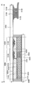
도 1a, 도 1b 및 도 1c는 각각 제1 실시예의 표시 장치의 일례를 도시하는 단면도, 제1 실시예의 표시 장치의 다른 일례를 나타내는 단면도, 제1 실시예의 표시 장치의 또 다른 일례를 나타내는 단면도이다.
도 2a, 도 2b 및 도 2c는 각각 제2 실시예의 반도체 장치의, 단면도, 등가 회로도, 상면도이다.
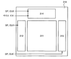
도 3a와 도 3b는 제3 실시예의 표시 장치의 전체를 도시하하는 블록도이다.
도 4는 제3 실시예의 표시 장치에서의 배선, 입력 단자 등의 배치를 도시하는 도면이다.
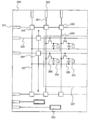
도 5는 시프트 레지스터 회로의 구성을 도시하는 블록도이다.
도 6은 플립플롭 회로의 일례를 도시하는 도면이다.
도 7은 플립플롭 회로의 레이아웃 도(상면도)를 도시하는 도면이다.
도 8은 시프트 레지스터 회로의 동작을 나타내기 위한 타이밍 차트를 도시하는 도면이다.
도 9의 (a) 내지 (c)는 제4 실시예의 반도체 장치의 제조 방법을 도시하는 도면이다.
도 10의 (a) 내지 (c)는 제4 실시예의 반도체 장치의 제조 방법을 도시하는 도면이다.
도 11은 제4 실시예의 반도체 장치의 제조 방법을 도시하는 도면이다.
도 12는 제4 실시예의 반도체 장치의 제조 방법을 도시하는 도면이다.
도 13은 제4 실시예의 반도체 장치의 제조 방법을 도시하는 도면이다.
도 14는 제4 실시예의 반도체 장치를 도시하는 도면이다.
도 15a 내지 도 15d는 제4 실시예의 반도체 장치를 도시하는 도면이다.
도 16은 제4 실시예의 반도체 장치를 도시하는 도면이다.
도 17은 제5 실시예의 반도체 장치를 도시하는 단면도이다.
도 18은 제6 실시예의 반도체 장치의 화소 등가 회로를 도시하는 도면이다.
도 19a 내지 도 19c는 제6 실시예의 반도체 장치를 도시하는 단면도이다.
도 20a와 도 20b는 각각 제6 실시예의 반도체 장치를 도시하는 상면도 및 단면도이다.
도 21a와 도 21b 및 도 21c는 제7 실시예의 반도체 장치를 도시하는 상면도 및 단면도이다.
도 22는 제7 실시예의 반도체 장치를 도시하는 단면도이다.
도 23a 내지 도 23d는 전자 장치들의 예를 도시하는 외관도이다.
도 24a와 도 24b는 텔레비전 장치 및 디지털 포토 프레임의 예를 각각 도시하는 외관도이다.
도 25a와 도 25b는 휴대 전화의 예를 도시하는 외관도이다.
도 26은 제9 실시예의 반도체 장치를 도시하는 단면도이다.Figs. 1A, 1B, and 1C are cross-sectional views showing one example of the display device of the first embodiment, a cross-sectional view showing another example of the display device of the first embodiment, and another example of the display device of the first embodiment .
2A, 2B and 2C are a cross-sectional view, an equivalent circuit diagram, and a top view, respectively, of the semiconductor device of the second embodiment.
3A and 3B are block diagrams showing the entire display device of the third embodiment.
4 is a diagram showing the arrangement of wirings, input terminals, and the like in the display device of the third embodiment.
5 is a block diagram showing the configuration of a shift register circuit.
6 is a diagram showing an example of a flip-flop circuit.
7 is a diagram showing a layout diagram (top view) of the flip-flop circuit.
8 is a timing chart showing the operation of the shift register circuit.
9A to 9C are diagrams showing a method of manufacturing the semiconductor device of the fourth embodiment.
10 (a) to 10 (c) are diagrams showing a manufacturing method of the semiconductor device of the fourth embodiment.
11 is a view showing a manufacturing method of the semiconductor device of the fourth embodiment.
12 is a view showing a manufacturing method of the semiconductor device of the fourth embodiment.
13 is a diagram showing a manufacturing method of the semiconductor device of the fourth embodiment.
14 is a diagram showing a semiconductor device of the fourth embodiment.
15A to 15D are diagrams showing the semiconductor device of the fourth embodiment.
16 is a view showing the semiconductor device of the fourth embodiment.
17 is a cross-sectional view showing the semiconductor device of the fifth embodiment.
18 is a diagram showing a pixel equivalent circuit of the semiconductor device of the sixth embodiment.
19A to 19C are sectional views showing the semiconductor device of the sixth embodiment.
20A and 20B are a top view and a cross-sectional view showing the semiconductor device of the sixth embodiment, respectively.
21A, 21B and 21C are a top view and a cross-sectional view showing the semiconductor device of the seventh embodiment.
22 is a cross-sectional view showing the semiconductor device of the seventh embodiment.
23A to 23D are external views showing examples of electronic devices.
24A and 24B are external views each showing an example of a television apparatus and a digital photo frame, respectively.
25A and 25B are external views showing an example of a cellular phone.
26 is a cross-sectional view showing the semiconductor device of the ninth embodiment.
이하, 실시예들을 설명한다. 본 발명은 이하의 설명으로 한정되지 않고, 본 발명의 사상 및 범위로부터 일탈하지 않고 모드와 상세를 다양하게 변경할 수 있다는 것은 당업자라면 용이하게 이해한다. 따라서, 본 발명은 후술하는 실시예들의 기재 내용으로 한정해서 해석되지 않는다.Hereinafter, embodiments will be described. It is to be understood by those skilled in the art that the present invention is not limited to the following description, and that modes and details can be variously changed without departing from the spirit and scope of the present invention. Therefore, the present invention is not construed as being limited to the description of the embodiments described later.
제1 실시예First Embodiment
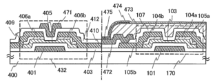
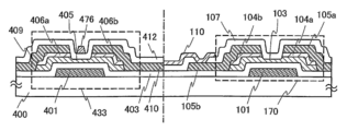
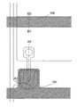
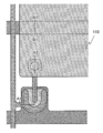
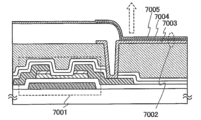
도 1a는 구동 회로를 위해 사용되는 제1 박막 트랜지스터(430) 및 화소부를 위해 사용되는 제2 박막 트랜지스터(170)를 동일 기판 위에 배치하는 일례를 도시한다. 또한, 도 1a은 표시 장치의 단면도의 일례라는 점에 주목한다.1A shows an example in which a first
화소부와 구동 회로는 동일 기판 위에 형성된다. 화소부에서는, 매트릭스 형상으로 배치된 인핸스먼트형 트랜지스터인 제2 박막 트랜지스터(170)를 사용해서 화소 전극(110)에 인가되는 전압의 온/오프를 전환한다. 이 화소부에 배치된 제2 박막 트랜지스터(170)는 산화물 반도체층(103)을 사용하여 형성된다. 제2 박막 트랜지스터의 전기적 특성은, 게이트 전압 ±20V에서 온/오프 비가 109 이상이기 때문에, 표시 콘트라스트를 개선할 수 있고, 또한 누설 전류가 적기 때문에, 저소비 전력 구동을 실현할 수 있다. 온/오프 비는 오프 전류에 대한 온 전류의 비(ION/IOFF)이며, ION/IOFF의 값이 클수록, 스위칭 특성이 우수하다. 따라서, 높은 온/오프 비는 표시 콘트라스트의 개선에 기여한다. 온 전류는 트랜지스터가 온 상태에 있을 때 소스 전극과 드레인 전극 사이에 흐르는 전류라는 점에 주목한다. 한편, 오프 전류는 트랜지스터가 오프 상태에 있을 때 소스 전극과 드레인 전극 사이에 흐르는 전류라는 점에 주목한다. 예를 들어, n채널 트랜지스터에서, 오프 전류는 게이트 전압이 트랜지스터의 임계 전압보다 낮을 때 소스 전극과 드레인 전극 사이에 흐르는 전류이다. 따라서, 고 콘트라스트 및 저소비 전력 구동을 실현하기 위해서는 화소부에 인핸스먼트형 트랜지스터를 사용하는 것이 바람직하다.The pixel portion and the driving circuit are formed on the same substrate. In the pixel portion, on / off of the voltage applied to the
구동 회로에서는, 산화물 반도체층(405) 아래에 제1 게이트 전극(401)과 산화물 반도체층(405) 위에 제2 게이트 전극(470)을 갖는 박막 트랜지스터(430)를 적어도 하나 사용한다. 제2 게이트 전극(470)을 백 게이트 전극이라고도 칭할 수 있다. 백 게이트 전극을 형성함으로써, 박막 트랜지스터의 신뢰성을 조사하기 위한 바이어스-열 스트레스 시험(이하, BT 시험이라 함)에서, BT 시험 전후 사이의 박막 트랜지스터의 임계 전압의 변화량을 저감할 수 있다.In the driving circuit, at least one
박막 트랜지스터(430)의 구조를 도 1a을 참조하여 설명한다. 절연 표면을 갖는 기판(400) 위에 설치된 제1 게이트 전극(401)은 제1 게이트 절연층(403)으로 덮히고, 제1 게이트 전극(401)과 겹치는 제1 게이트 절연층(403) 위에는 산화물 반도체층(405)이 설치된다. 산화물 반도체층(405) 위에는, 제1 배선(409)과 제2 배선(410)이 설치된다. 산화물 반도체층(405)은, 소스 전극 또는 드레인 전극으로서 기능하며 제1 배선(409) 및 제2 배선(410)과 겹치는 영역의 두께보다 얇은 두께의 영역을 포함한다. 산화물 반도체층(405)에서의 얇은 두께의 영역 위에 그리고 그 영역과 접하도록 제2 게이트 절연층(412)이 설치된다. 또한, 제2 게이트 절연층(412) 위에 제2 게이트 전극(470)이 설치된다.The structure of the
산화물 반도체층(405)은, 예를 들어, In2O3:Ga2O3:ZnO = 1:1:1(In:Ga:Zn = 1:1:0.5)인 타겟을 사용하는 스퍼터링법에 의해 아르곤 가스 유량을 10sccm으로 하고 산소 유량을 5sccm으로 하여 형성된다. 또한, 산화물 반도체층(405)과 제1 배선(409) 사이에는 n+층(406a)을 설치하고, 산화물 반도체층(405)과 제2 배선(410) 사이에는 n+층(406b)을 설치한다.The
본 실시예에서, 소스 영역 및 드레인 영역으로서 기능하는 n+층(406a, 406b)은 In-Ga-Zn-O계 비 단결정막이며, 이는 산화물 반도체층(405)의 형성 조건과는 다른 형성 조건에서 형성되고 저 저항의 산화물 반도체층이다. 예를 들어, 아르곤 가스 유량을 40sccm으로 한 조건에서 얻어지는 산화물 반도체층으로 형성된 n+층(406a, 406b)은 n형의 도전성 및 0.01eV 내지 0.1eV의 활성화 에너지(ΔE)를 갖는다. 본 실시예에서, n+층(406a, 406b)은 In-Ga-Zn-O계 비 단결정막이며, 적어도 비정질 성분을 포함한다는 점에 주목한다. n+층(406a, 406b)은 비정질 성분에 결정립(나노 결정)을 포함하는 경우가 있다. n+층(406a, 406b)에 포함된 결정립(나노 결정)의 직경은 1nm 내지 10nm, 통상적으로는 2nm 내지 4nm 정도이다.In the present embodiment, the n + layers 406a and 406b functioning as the source region and the drain region are non-monocrystalline films of In-Ga-Zn-O system, which are different from the formation conditions of the
또한, 제1 게이트 전극(401)과 제2 게이트 전극(470)은 동 전위를 갖도록 전기적으로 접속되어도 된다. 제1 게이트 전극(401)과 제2 게이트 전극(470)이 동 전위를 가지면, 산화물 반도체층의 위 및 아래 측으로부터 게이트 전압을 인가할 수 있어서, 온 상태에서 흐르는 전류의 양을 증가시킬 수 있다.The
또한, 임계 전압을 음의 값으로 시프트하기 위한 제어 신호선을 제1 게이트 전극(401) 또는 제2 게이트 전극(470)에 전기적으로 접속함으로써, 디플리션형 TFT를 형성할 수 있다. Further, a control signal line for shifting the threshold voltage to a negative value is electrically connected to the
대안으로, 임계 전압을 양의 값으로 시프트하기 위한 제어 신호선을 제1 게이트 전극(401) 또는 제2 게이트 전극(470)에 전기적으로 접속함으로써, 인핸스먼트형 TFT를 형성해도 된다.Alternatively, an enhancement type TFT may be formed by electrically connecting a control signal line for shifting the threshold voltage to a positive value to the
또한, 구동 회로에 사용하는 2개의 박막 트랜지스터의 조합은 특별히 한정되지 않으며, 1개의 게이트 전극을 갖는 박막 트랜지스터를 디플리션형 TFT로서 사용하고 2개의 게이트 전극을 갖는 박막 트랜지스터를 인핸스먼트형 TFT로서 사용하는 조합을 이용해도 된다. 그 경우에, 화소부의 박막 트랜지스터는 게이트 전극이 산화물 반도체층의 위 및 아래에 각각 배치된 구조를 갖는다.The combination of the two thin film transistors used in the driving circuit is not particularly limited and a thin film transistor having one gate electrode is used as a depletion type TFT and a thin film transistor having two gate electrodes is used as an enhancement type TFT May be used. In that case, the thin film transistor of the pixel portion has a structure in which the gate electrode is disposed above and below the oxide semiconductor layer, respectively.
대안으로, 화소부의 박막 트랜지스터는 게이트 전극이 산화물 반도체층의 위 및 아래에 각각 배치된 구조를 가져도 되고, 구동 회로의 인핸스먼트형 TFT와 디플리션형 TFT의 각각은 게이트 전극이 산화물 반도체층의 위 및 아래에 각각 배치된 구조를 가져도 된다. 그 경우에는, 임계 전압을 제어하기 위한 제어 신호선을 상측 게이트 전극과 하측 게이트 전극 중 어느 하나에 전기적으로 접속시키고 접속된 게이트 전극이 임계 전압을 제어하는 구성을 채용한다. Alternatively, the thin film transistor of the pixel portion may have a structure in which the gate electrode is disposed above and below the oxide semiconductor layer, and each of the enhancement type TFT and the depletion type TFT of the drive circuit has a structure in which the gate electrode And may have structures arranged above and below, respectively. In this case, the control signal line for controlling the threshold voltage is electrically connected to either the upper gate electrode or the lower gate electrode, and the connected gate electrode controls the threshold voltage.
도 1a에서, 제2 게이트 전극(470)은 공정 수를 줄이기 위해 예를 들어 투과형의 액정 표시 장치의 경우 투명 도전막을 사용하여 화소부의 화소 전극(110)과 동일한 재료로 형성된다는 점에 주목한다. 그러나, 제2 게이트 전극(470)이 이러한 예로 특별히 한정되지는 않는다. 또한, 제2 게이트 전극(470)의 폭은 제1 게이트 전극(401)의 폭보다 넓고 또한 산화물 반도체층의 폭보다 넓은 예를 도시하고 있지만, 제2 게이트 전극(470)의 폭이 이러한 예로 특별히 한정되지는 않는다. 제1 게이트 전극(401)의 폭은 산화물 반도체층의 두께가 얇은 영역의 폭보다 넓다는 점에 주목한다.1A, the
도 1b는 제2 게이트 전극의 재료 및 폭이 도 1a과는 다른 예를 도시한다. 또한, 도 1b는 유기 발광 소자 또는 무기 발광 소자에 접속되는 제2 박막 트랜지스터(170)가 화소부에 포함된 표시 장치의 일례이다.Fig. 1B shows an example in which the material and width of the second gate electrode are different from those in Fig. 1A. 1B is an example of a display device in which a pixel portion includes a second
도 1b에서, 박막 트랜지스터(432)의 제2 게이트 전극으로서 기능하는 전극(471)의 재료로는, 금속 재료(알루미늄(Al), 구리(Cu), 티타늄(Ti), 탄탈륨(Ta), 텅스텐(W), 몰리브덴(Mo), 크롬(Cr), 네오디뮴(Nd), 스칸듐(Sc) 중에서 선택되는 원소 또는 상술한 원소들 중 임의의 것을 성분으로 하는 합금)를 사용한다. 단면에서의 전극(471)의 폭은 도 1a의 제2 게이트 전극(470)의 폭보다 작다. 또한, 전극(471)의 폭은 산화물 반도체층의 폭보다 작다. 전극(471)의 폭을 좁게 함으로써, 전극(471)이 제2 게이트 절연층(412)을 개재하여 제1 배선(409) 및 제2 배선(410)과 겹치는 면적을 저감할 수 있어서, 기생 용량을 작게 할 수 있다. 도 1b에서, 전극(471)의 폭은 산화물 반도체층의 두께가 얇은 영역의 폭보다 넓다는 점에 주목한다.1B, the
발광 소자는 적어도 제1 전극(472), 발광층(475), 제2 전극(474)을 포함한다. 도 1b에서, 전극(471)은 공정 수를 줄이기 위해 화소부의 제1 전극(472)과 동일한 재료, 예를 들어, 알루미늄 등을 사용하여 형성되지만, 전극(471)이 이러한 예로 특별히 한정되지는 않는다. 또한, 도 1b에서, 절연층(473)은 서로 인접하는 화소들의 제1 전극과의 절연을 도모하기 위한 격벽으로서 기능한다.The light emitting device includes at least a first electrode 472, a light emitting layer 475, and a
또한, 도 1c는 제2 게이트 전극의 재료 및 폭이 도 1a와는 다른 일례를 도시한다. 도 1c에서, 박막 트랜지스터(433)의 제2 게이트 전극으로서 기능하는 전극(476)의 재료로는, 금속 재료(알루미늄(Al), 구리(Cu), 티타늄(Ti), 탄탈륨(Ta), 텅스텐(W), 몰리브덴(Mo), 크롬(Cr), 네오디뮴(Nd), 스칸듐(Sc) 중에서 선택되는 원소 또는 상술한 원소들 중 임의의 것을 성분으로 하는 합금)을 사용한다. 단면에서의 제2 게이트 전극의 폭은 도 1b의 경우보다 좁다. 그 폭을 도 1b의 경우보다 좁게 함으로써, 제2 게이트 절연층(412)을 개재하여 제1 배선(409) 및 제2 배선(410)과 겹치지 않도록 제2 게이트 전극을 형성할 수 있고, 이에 따라 기생 용량을 더욱 줄일 수 있다. 도 1c에 도시한 전극(476)의 폭은 산화물 반도체층의 두께가 얇은 영역의 폭보다 좁다. 이렇게 좁은 폭의 전극(476)을 형성하는 경우에는, 레지스트 마스크의 단부보다 내측에 전극(476)의 양단이 위치하도록 습식 에칭 등을 사용하는 공정을 수행하는 것이 바람직하다. 그러나, 도 1c에서는, 화소 전극(110)의 금속 재료와는 다른 금속 재료를 사용하므로, 전극(476)을 형성하기 위해 포토리소그래피 공정이 1회 더 추가되고, 마스크 수도 1장 더 필요하다.1C shows an example in which the material and width of the second gate electrode are different from those in Fig. 1A. 1C, the
게이트선 구동 회로나 소스선 구동 회로 등의 주변 회로, 또는 액정 표시 장치, 발광 표시 장치 또는 전자 페이퍼를 위해 사용되는 화소부에 대하여, 위 및 아래의 2개의 게이트 전극 사이에 끼워진 산화물 반도체를 포함하는 박막 트랜지스터를 사용함으로써, 고속 구동이나 저 전력 소비를 도모할 수 있는다. 또한, 공정 수를 대폭 증가시키지 않고 동일 기판 위에 화소부와 구동 회로 모두를 설치할 수 있다. 동일 기판 위에 화소부 외에도 다양한 회로들을 설치함으로써, 표시 장치의 제조 비용을 저감할 수 있다.A peripheral circuit such as a gate line driving circuit or a source line driving circuit or a pixel portion used for a liquid crystal display device, a light emitting display device, or an electronic paper, an oxide semiconductor sandwiched between two upper and lower gate electrodes By using the thin film transistor, high-speed driving and low power consumption can be achieved. Further, both the pixel portion and the driving circuit can be provided on the same substrate without significantly increasing the number of process steps. By providing various circuits besides the pixel portion on the same substrate, the manufacturing cost of the display device can be reduced.
제2 실시예Second Embodiment
제1 실시예에서는 구동 회로의 박막 트랜지스터로서 하나의 박막 트랜지스터를 설명하였지만, 제2 실시예에서는 2개의 n채널형 박막 트랜지스터를 사용해서 구동 회로의 인버터 회로를 형성하는 일례를 이하에서 설명한다. 도 2a에 도시한 박막 트랜지스터는 제1 실시예의 도 1a에 도시한 박막 트랜지스터(430)와 동일하기 때문에, 동일한 부분에는 동일한 참조 부호를 사용해서 설명한다.In the first embodiment, one thin film transistor is described as the thin film transistor of the driving circuit. In the second embodiment, an example of forming the inverter circuit of the driving circuit by using two n-channel thin film transistors is described below. 2A is the same as that of the
화소부를 구동하기 위한 구동 회로는 인버터 회로, 커패시터, 저항 등을 사용해서 형성된다. 2개의 n채널 TFT를 조합해서 인버터 회로를 형성하는 경우, 인핸스먼트형 트랜지스터와 디플리션형 트랜지스터를 조합한 인버터 회로(이하, EDMOS 회로라고 칭함) 및 2개의 인핸스먼트형 TFT를 조합한 인버터 회로(이하, EEMOS 회로라 칭함)가 있다. A driving circuit for driving the pixel portion is formed by using an inverter circuit, a capacitor, a resistor, or the like. When an inverter circuit is formed by combining two n-channel TFTs, an inverter circuit (hereinafter referred to as an EDMOS circuit) combining an enhancement type transistor and a depletion type transistor and an inverter circuit Hereinafter referred to as an EEMOS circuit).
구동 회로의 인버터 회로의 단면 구조를 도 2a에 도시한다. 도 2a 내지 도 2c에 도시한 박막 트랜지스터(430)와 제2 박막 트랜지스터(431)는 보텀 게이트형 박막 트랜지스터이며, 반도체층 위로 소스 영역과 드레인 영역을 개재하여 배선이 설치되어 있는 박막 트랜지스터의 예라는 점에 주목한다. The cross-sectional structure of the inverter circuit of the driving circuit is shown in Fig. The
도 2a에서는, 기판(400) 위로 제1 게이트 전극(401) 및 게이트 전극(402)을 설치한다. 제1 게이트 전극(401) 및 게이트 전극(402)은, 몰리브덴, 티타늄, 크롬, 탄탈륨, 텅스텐, 알루미늄, 구리, 네오디뮴, 스칸듐 등의 금속 재료 또는 이러한 금속 재료들 중 임의의 것을 주성분으로 하는 합금 재료를 사용하여 단층 구조 또는 적층 구조를 갖도록 형성될 수 있다. 2A, a
예를 들어, 제1 게이트 전극(401) 및 게이트 전극(402)의 2층 적층 구조로는, 알루미늄층 위에 몰리브덴층이 적층된 2층 적층 구조, 구리층 위에 몰리브덴층이 적층된 2층 적층 구조, 구리층 위에 질화 티타늄층 혹은 질화 탄탈륨층이 적층된 2층 적층 구조, 또는 질화 티타늄층과 몰리브덴층이 적층된 2층 적층 구조가 바람직하다. 3층 적층 구조로는, 텅스텐층 또는 질화 텅스텐층의 적층, 알루미늄과 실리콘의 합금 또는 알루미늄과 티타늄의 합금, 질화 티타늄층 또는 티타늄층을 적층한 적층이 바람직하다. For example, the two-layer structure of the
또한, 제1 게이트 전극(401) 및 게이트 전극(402)을 덮는 제1 게이트 절연층(403) 위에는 산화물 반도체층(405)과 제2 산화물 반도체층(407)을 설치한다.An
산화물 반도체층(405) 위로는 제1 배선(409) 및 제2 배선(410)을 설치하고, 제2 배선(410)은 제1 게이트 절연층(403)에 형성된 콘택트 홀(404)을 통해 게이트 전극(402)에 직접 접속된다. 또한, 제2 산화물 반도체층(407) 위로는 제3 배선(411)을 설치한다.The
박막 트랜지스터(430)는, 제1 게이트 전극(401), 및 제1 게이트 절연층(403)을 개재하여 제1 게이트 전극(401)과 겹치는 산화물 반도체층(405)을 포함한다. 제1 배선(409)은 음의 전압 VDL이 인가되는 전원선(음의 전원선)이다. 이 전원선은 접지 전위의 전원선(접지 전원선)이어도 된다. The
또한, 제2 박막 트랜지스터(431)는, 게이트 전극(402), 및 제1 게이트 절연층(403)을 개재하여 게이트 전극(402)과 겹치는 제2 산화물 반도체층(407)을 포함한다. 제3 배선(411)은 양의 전압 VDH가 인가되는 전원선(양의 전원선)이다.The second
또한, 제2 산화물 반도체층(407)과 제2 배선(410) 사이에는 n+층(408a)을 설치하고, 제2 산화물 반도체층(407)과 제3 배선(411) 사이에는 n+층(408b)을 설치한다.In addition, the between the second
또한, 구동 회로의 인버터 회로의 상면도를 도 2c에 도시한다. 도 2c에서, 쇄선 Z1-Z2를 따라 절단한 단면이 도 2a에 해당한다.Fig. 2C shows a top view of the inverter circuit of the drive circuit. In Fig. 2C, a section cut along the chain line Z1-Z2 corresponds to Fig. 2A.
또한, EDMOS 회로의 등가 회로를 도 2b에 도시한다. 도 2a에 도시한 회로 접속은, 도 2b에 해당하고, 박막 트랜지스터(430)가 인핸스먼트형 n채널 트랜지스터이며 제2 박막 트랜지스터(431)가 디플리션형 n채널 트랜지스터인 일례이다. An equivalent circuit of the EDMOS circuit is shown in Fig. 2B. The circuit connection shown in Fig. 2A corresponds to Fig. 2B, and is an example in which the
본 실시예에서는, 박막 트랜지스터(430)가 인핸스먼트형의 n채널 트랜지스터로서 기능할 수 있도록, 산화물 반도체층(405) 위로 제2 게이트 절연층(412)을 설치하고, 제2 게이트 절연층(412) 위로 제2 게이트 전극(470)을 설치하여, 제2 게이트 전극(470)에 인가하는 전압에 의해 박막 트랜지스터(430)의 임계값을 제어한다.The second
또한, 제2 게이트 절연층(412)은 제2 산화물 반도체층(407)을 덮는 보호층으로서 기능한다. Further, the second
도 2a 및 도 2c에서는, 제1 게이트 절연층(403)에 형성된 콘택트 홀(404)을 통해 제2 배선(410)이 게이트 전극(402)에 직접 접속되는 예를 도시하고 있지만, 특별히 한정되지 않고, 접속 전극을 별도 설치하여 제2 배선(410)과 게이트 전극(402)을 전기적으로 접속시켜도 된다는 점에 주목한다.2A and 2C show an example in which the
또한, 본 실시예는 제1 실시예와 자유롭게 조합할 수 있다.The present embodiment can be freely combined with the first embodiment.
제3 실시예Third Embodiment
제3 실시예에서는, 표시 장치를 블록도 등을 참조하여 설명한다.In the third embodiment, a display device will be described with reference to a block diagram or the like.
도 3a는 액티브 매트릭스 액정 표시 장치의 블록도의 일례를 도시한다. 도 3a에 도시한 액정 표시 장치는, 기판(300) 위에, 표시 소자를 구비한 화소를 복수 갖는 화소부(301), 각 화소의 게이트 전극에 접속된 주사선을 각각 제어하는 주사선 구동 회로(302), 및 선택된 화소에 입력되는 비디오 신호를 제어하는 신호선 구동 회로(303)를 포함한다. Fig. 3A shows an example of a block diagram of an active matrix liquid crystal display device. 3A includes a
도 3b는 액티브 매트릭스 발광 표시 장치의 블록도의 일례를 도시한다. 도 3b에 도시한 발광 표시 장치는, 기판(310) 위에, 표시 소자를 구비한 화소를 복수 갖는 화소부(311), 화소의 게이트 전극에 접속된 주사선을 제어하는 제1 주사선 구동 회로(312)와 제2 주사선 구동 회로(313), 및 선택된 화소에 입력되는 비디오 신호를 제어하는 신호선 구동 회로(314)를 포함한다. 하나의 화소에 스위칭용 TFT(Thin Film Transistor)와 전류 제어용 TFT인 2개의 TFT를 배치하는 경우, 도 3b에 도시한 발광 표시 장치에서는, 스위칭용 TFT의 게이트 전극에 접속된 제1 주사선에 입력되는 신호를 제1 주사선 구동 회로(312)에서 생성하고, 전류 제어용 TFT의 게이트 전극에 접속된 제2 주사선에 입력되는 신호를 제2 주사선 구동 회로(313)에서 생성한다. 제1 주사선에 입력되는 신호 및 제2 주사선에 입력되는 신호를 하나의 주사선 구동 회로에서 생성하는 구조를 채용해도 된다는 점에 주목한다. 대안으로, 예를 들어, 스위칭 소자에 포함된 TFT의 수에 따라, 스위칭 소자의 동작을 제어하는 데 사용되는 복수의 제1 주사선이 각 화소에 설치되어 있어도 된다. 이 경우, 복수의 제1 주사선에 입력되는 모든 신호를, 하나의 주사선 구동 회로에서 생성해도 되고, 또는 복수의 주사선 구동 회로에 의해 개별적으로 생성해도 된다.3B shows an example of a block diagram of an active matrix light emitting display. 3B includes a
또한, 여기에서는, 주사선 구동 회로(302), 제1 주사선 구동 회로(312), 제2 주사선 구동 회로(313) 및 신호선 구동 회로(303, 314)를 표시 장치에 형성하는 형태를 설명하고 있지만, 주사선 구동 회로(302), 제1 주사선 구동 회로(312) 또는 제2 주사선 구동 회로(313)의 일부를 IC 등의 반도체 장치를 이용하여 실장해도 된다는 점에 주목한다. 대안으로, 신호선 구동 회로(303 또는 314)의 일부를 IC 등의 반도체 장치를 이용하여 실장해도 된다.Although the description has been given of the mode in which the scanning
도 4는, 표시 장치를 구성하는, 신호 입력 단자(321), 주사선(323), 신호선(324), 비선형 소자를 포함하는 보호 회로 및 화소부 간의 위치 관계를 도시하는 도면이다. 화소부(327)는, 절연 표면을 갖는 기판(320) 위로 서로 교차 배치된 주사선(323)과 신호선(324)을 포함한다. 화소부(327)는 도 3a와 도 3b에 도시한 화소부(301)와 화소부(311)에 해당한다는 점에 주목한다. 4 is a diagram showing the positional relationship between the
화소부(301)는, 열 방향으로 배치되고 신호선 구동 회로(303)로부터 연장되는 복수의 신호선 S1 내지 Sm(도시하지 않음)에 의해 신호선 구동 회로(303)에 접속되고, 행 방향으로 배치되고 주사선 구동 회로(302)로부터 연장되는 복수의 주사선 G1 내지 Gn(도시하지 않음)에 의해 주사선 구동 회로(302)에 접속된다. 화소부(301)는 신호선 S1 내지 Sm 및 주사선 G1 내지 Gn에 의해 매트릭스 형상으로 배치된 복수의 화소(도시하지 않음)를 포함한다. 이어서, 각 화소는 신호선 Sj(신호선 S1 내지 Sm 중 임의의 하나) 및 주사선 Gi(주사선 G1 내지 Gn 중 임의의 하나)에 접속된다. The
화소부(327)는 매트릭스 형상으로 배치된 복수의 화소(328)를 포함한다. 화소(328)는 주사선(323)과 신호선(324)에 접속된 화소 TFT(329), 축적 용량(330) 및 화소 전극(331)을 포함한다.The
여기서 예시한 화소 구성은 축적 용량(330)의 하나의 전극이 화소 TFT(329)에 접속되고 다른 전극이 용량선(332)에 접속되는 경우이다. 또한, 화소 전극(331)은 표시 소자(액정 소자, 발광 소자, 콘트라스트 매체(전자 잉크) 등)를 구동하는 한 전극으로서 기능한다. 이러한 표시 소자의 다른 전극은 공통 단자(333)에 접속된다.The pixel configuration exemplified here is a case in which one electrode of the
일부 보호 회로는 화소부(327)와 신호선 입력 단자(322) 사이에 배치되어 있다. 또한, 다른 보호 회로는 주사선 구동 회로와 화소부(327) 사이에 배치되어 있다. 본 실시예에서는, 복수의 보호 회로를 배치하여, 정전기 등으로 인해 서지 전압이 주사선(323), 신호선(324), 용량 버스선(337)에 인가될 때 화소 TFT(329) 등이 파괴되지 않는다. 따라서, 보호 회로는 서지 전압이 인가될 때 공통 배선에 전하가 방출되도록 구성되어 있다.Some of the protection circuits are disposed between the
본 실시예에서는, 주사선(323) 측, 신호선(324) 측, 용량 버스선(337) 측에 보호 회로(334), 보호 회로(335), 보호 회로(336)를 각각 배치한 예를 나타내고 있다. 보호 회로의 배치 위치는 이에 한정되지 않는다는 점에 주목한다. 또한, IC 등의 반도체 장치를 이용하여 주사선 구동 회로를 실장하지 않는 경우에는, 주사선(323) 측에 보호 회로(334)를 설치하지 않아도 된다.The present embodiment shows an example in which the
이러한 회로들에 대하여 제1 실시예 또는 제2 실시예에서 설명한 TFT를 사용함으로써, 이하와 같은 이점들을 얻을 수 있다. By using the TFT described in the first embodiment or the second embodiment for these circuits, the following advantages can be obtained.
구동 회로는 논리 회로부 및 스위치부 또는 버퍼부로 크게 구별된다. 논리 회로부에 설치되는 TFT는 임계 전압을 제어할 수 있는 구조를 갖는 것이 바람직하다. 반면, 스위치부 또는 버퍼부에 설치되는 TFT는 큰 온 전류를 갖는 것이 바람직하다. 제1 실시예 또는 제2 실시예에서 설명한 TFT를 갖는 구동 회로를 설치함으로써, 논리 회로부에 설치되는 TFT의 임계 전압을 제어할 수 있고, 스위치부 또는 버퍼부에 설치되는 TFT의 온 전류를 증가시킬 수 있다. 또한, 제1 실시예 또는 제2 실시예에서 설명한 TFT는 구동 회로가 점유하는 면적을 작게 하고 프레임을 좁게 하는 데 기여한다. The driving circuit is largely divided into a logic circuit portion and a switch portion or a buffer portion. The TFT provided in the logic circuit portion preferably has a structure capable of controlling the threshold voltage. On the other hand, the TFT provided in the switch unit or the buffer unit preferably has a large ON current. The threshold voltage of the TFT provided in the logic circuit portion can be controlled and the ON current of the TFT provided in the switch portion or the buffer portion can be increased by providing the drive circuit having the TFT described in the first embodiment or the second embodiment . In addition, the TFTs described in the first or second embodiment contribute to making the area occupied by the driving circuit small and narrowing the frame.
이하, 주사선 구동 회로에 포함된 시프트 레지스터 회로를 설명한다. 도 5에 도시한 시프트 레지스터 회로는, 복수의 플립플롭 회로(351), 제어 신호선(352), 제어 신호선(353), 제어 신호선(354), 제어 신호선(355), 제어 신호선(356) 및 리셋선(357)을 포함한다. Hereinafter, the shift register circuit included in the scanning line driving circuit will be described. The shift register circuit shown in Fig. 5 includes a plurality of flip-
도 5의 시프트 레지스터 회로에 도시한 바와 같이, 플립플롭 회로(351)에서는, 제1 단의 입력 단자 IN에 제어 신호선(352)을 통해 스타트 펄스 SSP가 입력되고, 다음 단의 입력 단자 IN에 이전 단의 플립플롭 회로(351)의 출력 신호 단자 SOUT이 접속되어 있다. 또한, N번째 단(N은 자연수)의 리셋 단자 RES는 리셋선(357)을 통해 (N+3)번째 단의 플립플롭 회로의 출력 신호 단자 SOUT에 접속되어 있다. 제어 신호선(353)을 통해 N번째 단의 플립플롭 회로(351)의 클록 단자 CLK에 제1 클록 신호 CLK1이 입력된다고 가정하면, (N+1)번째 단의 플립플롭 회로(351)의 클록 단자 CLK에는 제어 신호선(354)을 통해 제2 클록 신호 CLK2가 입력된다. (N+2)번째 단의 플립플롭 회로(351)의 클록 단자 CLK에는 제어 신호선(355)을 통해 제3 클록 신호 CLK3이 입력된다. (N+3)번째 단의 플립플롭 회로(351)의 클록 단자 CLK에는 제어 신호선(356)을 통해 제4 클록 신호 CLK4가 입력된다. 이어서, (N+4)번째 단의 플립플롭 회로(351)의 클록 단자 CLK에는 제어 신호선(353)을 통해 제1 클록 신호 CLK1이 입력된다. 또한, N번째 단의 플립플롭 회로(351)는 게이트 출력 단자 GOUT으로부터 N번째 단의 플립플롭 회로의 출력 SRoutN을 출력한다.5, in the flip-
플립플롭 회로(351), 전원 및 전원선 간의 접속은 도시되어 있지 않으나, 각 플립플롭 회로(351)에는 전원선을 통해 전원 전위 Vdd 및 전원 전위 GND가 공급된다는 점에 주목한다.Note that the connection between the flip-
본 명세서에서 설명하는 전원 전위는 기준 전위가 0V인 경우의 전위차에 해당한다는 점에 주목한다. 따라서, 전원 전위를 전원 전압이라 칭하기도 하며, 또는 일부 경우에 전원 전압을 전원 전위라 칭하기도 한다.It is noted that the power source potential described in this specification corresponds to the potential difference when the reference potential is 0V. Therefore, the power source potential may be referred to as a power source voltage, or in some cases, the power source voltage may be referred to as a power source potential.
본 명세서에서, "A와 B가 서로 접속되어 있다"는 표현은 A와 B가 서로 직접 접속되어 있는 것 외에도 A와 B가 서로 전기적으로 접속되어 있는 경우를 포함한다는 점에 주목한다. 여기서, "A와 B가 서로 전기적으로 접속되어 있다"는 표현은, A와 B 사이에 어떠한 전기적 작용을 갖는 대상물이 존재할 때 그 대상물을 통해 A와 B가 대략 동일한 전위를 갖는 경우를 포함한다. 구체적으로, "A와 B가 서로 전기적으로 접속되어 있다"는 표현은, 회로 동작을 고려할 때 A와 B가 대략 동 전위를 갖는 것으로 고려하는 경우를 포함하며, 예를 들어, TFT와 같은 스위칭 소자를 통해 A와 B가 접속되고 그 스위칭 소자의 도통에 의해 A와 B가 대략 동 전위를 갖는 경우, 저항 소자를 통해 A와 B가 접속되고 저항 소자의 양단에서 발생하는 전위들 간의 전위차가 A와 B를 포함한 회로의 동작에 영향을 끼치지 않는 경우 등이 있다.Note that, in this specification, the expression "A and B are connected to each other" includes not only that A and B are directly connected to each other but also A and B are electrically connected to each other. Here, the expression " A and B are electrically connected to each other " includes a case where A and B have substantially the same potential through the object when there is an object having any electrical action between A and B. Specifically, the expression " A and B are electrically connected to each other " includes a case where A and B are considered to have substantially the same potential in consideration of circuit operation, and for example, A and B are connected through the resistance element and the potential difference between the potentials generated at both ends of the resistance element becomes A and B through the resistance element when A and B are connected through conduction of the switching element, And the case where the operation of the circuit including B is not affected.
다음으로, 도 6은 도 5에 도시한 시프트 레지스터 회로에 포함된 플립플롭 회로(351)의 일 형태를 도시한다. 도 6에 도시한 플립플롭 회로(351)는 논리 회로부(361)와 스위치부(362)를 포함한다. 논리 회로부(361)는 TFT(363 내지 368)를 포함한다. 또한, 스위치부(362)는 TFT(369 내지 372)를 포함한다. 논리 회로부는 외부로부터 입력되는 신호에 따라 후단의 회로인 스위치부에 출력되는 신호를 전환하기 위한 회로라는 점에 주목한다. 또한, 스위치부는, 외부 및 제어 회로부로부터 입력되는 신호에 따라 스위치로서 기능하는 TFT의 온/오프를 전환하고 그 TFT의 크기 및 구조에 따른 전류를 출력하기 위한 회로이다.Next, Fig. 6 shows one form of the flip-
플립플롭 회로(351)에서, 입력 단자 IN은 TFT(364)의 게이트 단자 및 TFT(367)의 게이트 단자에 접속되어 있다. 리셋 단자 RES는 TFT(363)의 게이트 단자에 접속되어 있다. 클록 단자 CLK는 TFT(369)의 제1 단자 및 TFT(371)의 제1 단자에 접속되어 있다. 전원 전위 Vdd가 공급되는 전원선은 TFT(364)의 제1 단자, TFT(366)의 게이트 단자와 제2 단자에 접속되어 있다. 전원 전위 GND가 공급되는 전원선은 TFT(363)의 제2 단자, TFT(365)의 제2 단자, TFT(367)의 제2 단자, TFT(368)의 제2 단자, TFT(370)의 제2 단자 및 TFT(372)의 제2 단자에 접속되어 있다. 또한, TFT(363)의 제1 단자, TFT(364)의 제2 단자, TFT(365)의 제1 단자, TFT(368)의 게이트 단자, TFT(369)의 게이트 단자 및 TFT(371)의 게이트 단자는 서로 접속되어 있다. TFT(366)의 제1 단자는 TFT(365)의 게이트 단자, TFT(367)의 제1 단자, TFT(368)의 제1 단자, TFT(370)의 게이트 단자 및 TFT(372)의 게이트 단자에 접속되어 있다. 또한, 게이트 출력 단자 GOUT는 TFT(369)의 제2 단자 및 TFT(370)의 제1 단자에 접속되어 있다. 출력 신호 단자 SOUT은 TFT(371)의 제2 단자 및 TFT(372)의 제1 단자에 접속되어 있다.In the flip-
여기에서는 TFT(363 내지 372)가 모두 n채널 TFT인 경우에 관하여 설명한다는 점에 주목한다.It is noted that the case where the
TFT는 게이트, 드레인, 소스인 적어도 세 개의 단자를 갖는 소자이며, 드레인 영역과 소스 영역 사이에 채널 형성 영역을 갖는다는 점에 주목한다. 드레인 영역, 채널 형성 영역, 소스 영역을 통해 전류가 흐를 수 있다. 여기서, 소스와 드레인은 일부 경우에 TFT의 구조, 동작 조건 등에 따라 서로 교체될 수 있으며, 따라서, 어느 것이 소스이며 어느 것이 드레인인지를 결정하는 것은 곤란하다. 따라서, 소스 및 드레인으로서 기능하는 영역들을, 소스 및 드레인이라 칭하지 않고, 예를 들어, 제1 단자 및 제2 단자라고 각각 칭하는 경우도 있다. 이 경우에, 게이트로서 기능하는 단자는 게이트 단자라 칭한다.Note that the TFT is an element having at least three terminals which are a gate, a drain, and a source, and has a channel forming region between the drain region and the source region. A current can flow through the drain region, the channel formation region, and the source region. Here, the source and the drain may be replaced with each other depending on the structure of the TFT, the operating conditions, etc. in some cases, and it is therefore difficult to determine which is the source and which is the drain. Therefore, the regions functioning as the source and the drain may be referred to as a first terminal and a second terminal, respectively, instead of being referred to as a source and a drain. In this case, a terminal functioning as a gate is referred to as a gate terminal.
이어서, 도 7은 도 6에 도시한 플립플롭 회로(351)의 레이아웃도의 일례를 도시한다.Next, Fig. 7 shows an example of the layout of the flip-
도 7의 플립플롭 회로는, 전원 전위 Vdd가 공급되는 전원선(381), 리셋선(382), 제어 신호선(353), 제어 신호선(354), 제어 신호선(355), 제어 신호선(356), 제어 신호선(383), 전원 전위 GND가 공급되는 전원선(384), 논리 회로부(361) 및 스위치부(362)를 포함한다. 논리 회로부(361)는 TFT(363 내지 368)를 포함한다. 스위치부(362)는 TFT(369 내지 372)를 포함한다. 도 7에서는, 게이트 출력 단자 GOUT에 접속되는 배선 및 출력 신호 단자 SOUT에 접속되는 배선도 도시하고 있다.The flip-flop circuit of FIG. 7 includes a
도 7은 반도체층(385), 제1 배선층(386), 제2 배선층(387), 제3 배선층(388), 콘택트 홀(389)을 도시한다. 제1 배선층(386)은 게이트 전극의 층에 의해 형성되고, 제2 배선층(387)은 TFT의 소스 전극 및 드레인 전극의 층에 의해 형성되고, 제3 배선층(388)은 화소부에서의 화소 전극의 층에 의해 형성되어도 된다는 점에 주목한다. 그러나, 이러한 예로 한정되지 않고, 예를 들어, 제3 배선층(388)을 화소 전극의 층과는 다른 층으로서 형성해도 된다.7 shows a
도 7의 회로 소자들 간의 접속 관계는 도 6에서 설명한 바와 같다는 점에 주목한다. 도 7에서는, 도 7은 제1 클록 신호가 입력되는 플립플롭 회로를 도시하고 있으므로, 제어 신호선(354 내지 356)에 대한 접속은 도시되어 있지 않다는 점에 주목한다. Note that the connection relationship between the circuit elements in Fig. 7 is as described in Fig. Note that, in Fig. 7, the flip-flop circuit in which the first clock signal is input is shown in Fig. 7, and thus the connection to the
도 7의 플립플롭 회로의 레이아웃도에서는, 논리 회로부(361)에 포함된 TFT(366) 또는 TFT(367)의 임계 전압을 제어함으로써, EDMOS 회로(373)를 형성할 수 있다. 통상적으로, TFT(366)가 디플리션형이고 TFT(367)가 인핸스먼트형인 EDMOS 회로(373)를 형성하고, 스위치부(362)에 포함된 TFT(369 내지 372)는 듀얼 게이트 TFT 또는 디플리션형 TFT이다. 도 6에서, EDMOS 회로(373)에서의 TFT(366)와 TFT(367)는 디플리션형 TFT의 게이트 전극의 접속 위치에 있어서 도 2a 내지 도 2c에 도시한 EDMOS 회로와는 다른 TFT이다.In the layout diagram of the flip-flop circuit of Fig. 7, the
TFT(366) 또는 TFT(367)를 듀얼 게이트 TFT로 되도록 형성하고 백 게이트 전극의 전위를 제어함으로써, 디플리션형 TFT 또는 인핸스먼트형 TFT를 형성할 수 있다. A depletion type TFT or an enhancement type TFT can be formed by forming the
도 7에서는, TFT(366)의 임계 전압을 제어하기 위한 백 게이트 전극과 동일한 전위를 갖는 제어 신호선(390)을 별도 설치하여 디플리션형을 형성한다. TFT(366)는 듀얼 게이트 TFT이며, 백 게이트 전극의 전위는 게이트 전극에 인가되는 전원 전위 Vdd가 공급되는 전원선(381)의 전위와는 다르다.7, a
도 7은, TFT(369 내지 372)가 듀얼 게이트 TFT이며, 백 게이트 전극들과 게이트 전극들이 동 전위를 갖는 일례를 도시하며, 백 게이트 전극들의 각각의 전위는 게이트 전극에 인가되는 전원 전위 Vdd가 공급되는 전원선의 전위와 동일한 전위이다. 7 shows an example in which the
이러한 식으로, 표시 장치의 화소부 및 구동 회로에 배치되는 TFT를, 산화물 반도체층을 사용한 n채널 TFT만으로 형성할 수 있다. In this way, the TFT disposed in the pixel portion and the driver circuit of the display device can be formed only of the n-channel TFT using the oxide semiconductor layer.
또한, 논리 회로부(361)의 TFT(366)는 전원 전위 Vdd에 따라 전류를 공급하기 위한 TFT이다. TFT(366)를 듀얼 게이트형 TFT 또는 디플리션형 TFT로 되도록 형성하여 흐르는 전류를 크게 함으로써, 성능 저하 없이 TFT의 소형화를 도모할 수 있다.The
또한, 스위치부(362)에 포함된 TFT에서, 그 TFT에 흐르는 전류량을 증가시킬 수 있고 온/오프의 전환을 고속으로 수행할 수 있기 때문에, 성능 저하 없이 TFT가 차지하는 면적을 축소할 수 있다. 따라서, TFT를 포함하는 회로가 차지하는 면적도 축소할 수 있다. 스위치부(362)의 TFT(369 내지 372)는 도면에 도시한 바와 같이 반도체층(385)을 제1 배선층(386)과 제3 배선층(388) 사이에 개재하도록 듀얼 게이트 TFT로 형성되어도 된다는 점에 주목한다.In addition, in the TFT included in the
도 7에서는, 듀얼 게이트 TFT의 각각이, 제1 배선층(386) 및 콘택트 홀(389)을 통해 서로 접속됨으로써 동일한 전위를 갖는 제3 배선층(388) 사이에 반도체층(385)을 개재하는 구조를 갖는 예를 도시하고 있다. 그러나, 이러한 예로 특별히 한정되지는 않으며, 예를 들어, 제3 배선층(388)에 대하여 제어 신호선을 별도로 설치하여 제3 배선층(388)의 전위를 제1 배선층(386)으로부터 독립하여 제어하는 구조도 가능하다.7 shows a structure in which each of the dual gate TFTs is connected to each other through the
도 7에 도시한 플립플롭 회로의 레이아웃도에서, TFT(363 내지 372)의 채널 형성 영역의 형상을 U자형(역 C자형 또는 말굽형)으로 해도 된다는 점에 주목한다. 또한, 도 7에서는, 모든 TFT가 동일한 크기를 갖지만, 후단의 부하량에 따라 출력 신호 단자 SOUT 또는 게이트 출력 단자 GOUT에 접속되는 각 TFT의 크기를 적절히 변경해도 된다. Note that, in the layout diagram of the flip-flop circuit shown in Fig. 7, the channel forming region of the
이어서, 도 5에 도시한 시프트 레지스터 회로의 동작을 도 8에 도시한 타이밍 차트를 참조하여 설명한다. 도 8은 도 5에 도시한 제어 신호선(352 내지 356)에 각각 공급되는 스타트 펄스 SSP, 제1 내지 제4 클록 신호 CLK1 내지 CLK4, 및 제1 내지 제5 단의 플립플롭 회로의 출력 신호 단자 SOUT으로부터 출력되는 SOUT1 내지 SOUT5를 도시한다. 도 8의 설명에서는 도 6과 도 7의 각 소자에 붙인 부호를 사용한다. Next, the operation of the shift register circuit shown in Fig. 5 will be described with reference to a timing chart shown in Fig. FIG. 8 is a timing chart of the start pulse SSP, the first to fourth clock signals CLK1 to CLK4, and the output signal terminal S of the flip-flop circuits of the first to fifth stages, which are respectively supplied to the
또한, 도 8은 플립플롭 회로에 포함된 TFT의 각각이 n채널 TFT인 경우의 타이밍 차트라는 점에 주목한다. 또한, 제1 클록 신호 CLK1은 도시한 바와 같이 제4 클록 신호 CLK4로부터 1/4 파장(점선에서 구분한 하나의 구간)만큼 시프트한 것이다.Note that Fig. 8 is a timing chart when each of the TFTs included in the flip-flop circuit is an n-channel TFT. Further, the first clock signal CLK1 is shifted from the fourth clock signal CLK4 by a quarter wavelength (one section separated from the dotted line) as shown in the figure.
우선, 기간 T1에서, 제1 단의 플립플롭 회로에는 스타트 펄스 SSP가 H 레벨로 입력되고, 논리 회로부(361)는 스위치부의 TFT(369, 371)를 턴온하고 TFT(370, 372)를 턴오프한다. 이때, 제1 클록 신호 CLK1은 L 레벨이므로, SOUT1은 L 레벨이다.First, in the period T1, the start pulse SSP is input to the flip-flop circuit of the first stage at H level and the
또한, 기간 T1에서, 제2 단 이후의 플립플롭 회로의 IN 단자에는 신호가 입력되지 않아서, 플립플롭 회로는 동작 없이 L 레벨을 출력한다는 점에 주목한다. 초기 상태에서는 시프트 레지스터 회로의 각 플립플롭 회로는 L 레벨을 출력하는 것으로서 가정하여 설명한다는 점에 주목한다.Note that, in the period T1, no signal is input to the IN terminal of the flip-flop circuit in the second and subsequent stages, and the flip-flop circuit outputs the L level without operation. Note that, in the initial state, each flip-flop circuit of the shift register circuit is assumed to output L level.
이어서, 기간 T2에서, 제1단의 플립플롭 회로에서는 기간 T1과 마찬가지로 논리 회로부(361)가 스위치부(362)를 제어한다. 기간 T2에서는, 제1 클록 신호 CLK1은 H 레벨이고, 따라서 SOUT1은 H 레벨이 된다. 또한, 기간 T2에서는, 제2 단의 플립플롭 회로의 IN 단자에 SOUT1이 H 레벨로 입력되고, 논리 회로부(361)가 스위치부의 TFT(369, 371)를 턴온하고 TFT(370, 372)를 턴오프한다. 이때, 제2 클록 신호 CLK2는 L 레벨이므로, SOUT2는 L 레벨이다. Subsequently, in the period T2, in the flip-flop circuit of the first stage, the
기간 T2에서, 제3단 이후의 플립플롭 회로의 IN 단자에는 신호가 입력되지 않기 때문에, 플립플롭 회로는 동작 없이 L 레벨을 출력한다는 점에 주목한다.Note that, in the period T2, since no signal is input to the IN terminal of the flip-flop circuit after the third stage, the flip-flop circuit outputs the L level without operation.
이어서, 기간 T3에서, 제1단의 플립플롭 회로에서 기간 T2의 상태를 유지하도록 논리 회로부(361)가 스위치부(362)를 제어한다. 따라서, 기간 T3에서는, 제1 클록 신호 CLK1은 H 레벨이며, SOUT1은 H 레벨이 된다. 또한, 기간 T3에서, 제2 단의 플립플롭 회로에서는 기간 T2와 마찬가지로 논리 회로부(361)가 스위치부(362)를 제어한다. 기간 T3에서, 제2 클록 신호 CLK2는 H 레벨이므로, SOUT2는 H 레벨이다. 또한, 기간 T3에서 제3 단의 플립플롭 회로의 IN 단자에는 SOUT2가 H 레벨로 입력되고, 논리 회로부(361)는 스위치부의 TFT(369, 371)를 턴온하고, TFT(370, 372)를 턴오프한다. 이때, 제3 클록 신호 CLK3은 L 레벨이기 때문에, SOUT3은 L 레벨이다. Subsequently, in the period T3, the
기간 T3에서, 제4 단 이후의 플립플롭 회로의 IN 단자에는 신호가 입력되지 않으므로, 플립플롭 회로는 동작 없이 L 레벨을 출력한다는 점에 주목한다. Note that, in the period T3, no signal is input to the IN terminal of the flip-flop circuit after the fourth stage, and therefore the flip-flop circuit outputs the L level without operation.
이어서, 기간 T4에서, 제1 단의 플립플롭 회로에서는 기간 T3의 상태를 유지하도록 논리 회로부(361)가 스위치부(362)를 제어한다. 따라서, 기간 T4에서, 제1 클록 신호 CLK1은 L 레벨이며 SOUT1은 L 레벨이 된다. 또한, 기간 T4에서, 제2 단의 플립플롭 회로에서는 기간 T3의 상태를 유지하도록 논리 회로부(361)가 스위치부(362)를 제어한다. 따라서, 기간 T4에서, 제2 클록 신호 CLK2는 H 레벨이며 SOUT2는 H 레벨이 된다. 또한, 기간 T4에서, 제3 단의 플립플롭 회로에서는, 기간 T3과 마찬가지로, 논리 회로부(361)가 스위치부(362)를 제어한다. 기간 T4에서, 제3 클록 신호 CLK3은 H 레벨이므로, SOUT3은 H 레벨이다. 또한, 기간 T4에서 제4 단의 플립플롭 회로의 IN 단자에는 SOUT3이 H 레벨로 입력되고, 논리 회로부(361)는 스위치부(362)의 TFT(369, 371)를 턴온하고, TFT(370, 372)를 턴오프한다. 이때, 제4 클록 신호 CLK4는 L 레벨이므로, SOUT4는 L 레벨이다. Subsequently, in the period T4, the
기간 T4에서, 제5 단 이후의 플립플롭 회로의 IN 단자에는 신호가 입력되지 않으므로, 플립플롭 회로는 동작 없이 L 레벨을 출력한다는 점에 주목한다.Note that, in the period T4, no signal is input to the IN terminal of the flip-flop circuit after the fifth stage, so that the flip-flop circuit outputs the L level without operation.
이어서, 기간 T5에서, 제2 단의 플립플롭 회로에서는, 기간 T3의 상태를 유지하도록 논리 회로부(361)가 스위치부(362)를 제어한다. 따라서, 기간 T5에서, 제2 클록 신호 CLK2는 L 레벨이며 SOUT2는 L 레벨이 된다. 또한, 기간 T5에서, 제3 단의 플립플롭 회로에서는, 기간 T4의 상태를 유지하도록 논리 회로부(361)가 스위치부(362)를 제어한다. 따라서, 기간 T5에서, 제3 클록 신호 CLK3은 H 레벨이며 SOUT3은 H 레벨이 된다. 또한, 기간 T5에서, 제4 단의 플립플롭 회로에서는, 기간 T4와 마찬가지로, 논리 회로부(361)가 스위치부(362)를 제어한다. 기간 T5에서, 제4 클록 신호 CLK4는 H 레벨이므로, SOUT4는 H 레벨이다. 또한, 제5 단 이후의 플립플롭 회로는, 제1 단 내지 제4 단의 플립플롭 회로와 마찬가지로 입력되는 신호의 배선 접속 및 타이밍을 갖기 때문에, 그 설명은 생략한다.Subsequently, in the period T5, in the second-stage flip-flop circuit, the
도 5의 시프트 레지스터 회로에 도시한 바와 같이, SOUT4는 제1 단의 플립플롭 회로의 리셋 신호로서 또한 기능한다. 기간 T5에서는, SOUT4가 H 레벨이 되고,이 신호는 제1 단의 플립플롭 회로의 리셋 단자 RES에 입력된다. 리셋 신호가 입력되면, 스위치부(362)의 TFT(369, 371)를 턴오프하고, TFT(370, 372)를 턴온한다. 이어서, 제1 단의 플립플롭 회로의 SOUT1은 다음 스타트 펄스 SSP가 입력될 때까지 L 레벨을 출력한다.As shown in the shift register circuit of Fig. 5, S OUT4 also functions as a reset signal of the flip-flop circuit of the first stage. In the period T5, S OUT4 becomes H level, and this signal is inputted to the reset terminal RES of the flip-flop circuit of the first stage. When the reset signal is input, the
전술한 동작에 의해, 제2 단 이후의 플립플롭 회로에서도, 후단의 플립플롭 회로로부터 출력되는 리셋 신호에 기초하여 논리 회로부를 리셋한다. SOUT1 내지 SOUT5로 도시한 바와 같이, 클록 신호의 1/4 파장만큼 시프트한 파형을 갖는 신호를 출력하는 시프트 레지스터 회로를 형성할 수 있다.According to the above-described operation, the logic circuit section is reset based on the reset signal output from the flip-flop circuit in the subsequent stage in the flip-flop circuit in the second and subsequent stages. A shift register circuit for outputting a signal having a waveform shifted by a quarter wavelength of the clock signal as shown by S OUT1 to S OUT5 can be formed.
인핸스먼트형 TFT와 디플리션형 TFT를 조합한 EDMOS 회로를 논리 회로부에 배치하고 듀얼 게이트 TFT를 스위치부에 배치한 구조를 플립플롭 회로가 갖는 경우, 논리 회로부(361)에 포함된 TFT에 흐르는 전류량을 증가시킬 수 있고, 성능 저하 없이 TFT가 차지하는 면적 및 TFT를 포함하는 회로가 차지하는 면적도 축소할 수 있다. 또한, 스위치부(362)에 포함된 TFT에서는, TFT에 흐르는 전류량을 증가시킬 수 있고, 온/오프의 전환을 고속으로 수행할 수 있기 때문에, 성능 저하 없이 TFT가 차지하는 면적 및 TFT를 포함하는 회로가 차지하는 면적도 축소할 수 있다. 따라서, 표시 장치의 프레임 협소화, 소형화, 고성능화를 도모할 수 있다. When the flip-flop circuit has a structure in which the EDMOS circuit in which the enhancement type TFT and the depletion type TFT are combined is arranged in the logic circuit portion and the dual gate TFT is arranged in the switch portion, the amount of current flowing in the TFT included in the
또한, 도 3a와 도 3b에 도시한 신호선 구동 회로에, 래치 회로, 레벨 시프터 회로 등을 설치할 수 있다. 신호선 구동 회로로부터 화소부에 신호를 보내는 최종 단에 버퍼부를 설치하고, 증폭된 신호를 신호선 구동 회로로부터 화소부에 보낸다. 따라서, 온 전류가 큰 TFT, 통상적으로는 듀얼 게이트형 TFT 또는 디플리션형 TFT를 버퍼부에 설치함으로써, TFT의 면적을 축소할 수 있고, 신호선 구동 회로가 차지하는 면적을 축소할 수 있다. 따라서, 표시 장치의 프레임 협소화, 소형화, 고성능화를 도모할 수 있다. 신호선 구동 회로의 일부인 시프트 레지스터는 고속 동작을 필요로 하므로, 시프트 레지스터는 IC 등을 사용해서 표시 장치에 실장하는 것이 바람직하다.In addition, a latch circuit, a level shifter circuit, and the like can be provided in the signal line driver circuit shown in Figs. 3A and 3B. A buffer unit is provided at the final stage for sending a signal from the signal line driver circuit to the pixel unit, and the amplified signal is sent from the signal line driver circuit to the pixel unit. Therefore, by providing a TFT having a large on-current, typically a dual-gate TFT or a depletion-type TFT in the buffer portion, the area of the TFT can be reduced and the area occupied by the signal line driver circuit can be reduced. Therefore, it is possible to reduce the frame size, the size, and the performance of the display device. Since the shift register, which is a part of the signal line driver circuit, requires a high-speed operation, it is preferable that the shift register is mounted on a display device using an IC or the like.
또한, 본 실시예는 제1 실시예 또는 제2 실시예와 자유롭게 조합할 수 있다. Further, this embodiment can be freely combined with the first embodiment or the second embodiment.
제4 실시예Fourth Embodiment
본 실시예에서는, 제1 실시예에서 설명한 제2 박막 트랜지스터(170)를 포함하는 표시 장치의 제조 방법을 도 9의 (a) 내지 (c), 도 10의 (a) 내지 (c), 도 11, 도 12, 도 13, 도 14, 도 15a 내지 도 15d 및 도 16을 참조하여 설명한다. In this embodiment, a method of manufacturing a display device including the second
도 9a에서, 투광성을 갖는 기판(100)으로는, 바륨 붕규산 유리나 알루미노 붕규산 유리 등의 유리 기판을 사용할 수 있다. 9A, a glass substrate such as barium borosilicate glass or aluminoborosilicate glass can be used as the
계속해서, 도전층을 기판(100)의 전체 면에 형성한 후, 제1 포토리소그래피 공정에 의해 레지스트 마스크를 형성한다. 이어서, 에칭에 의해 불필요한 부분을 제거해서, 배선 및 전극(게이트 전극(101)을 포함하는 게이트 배선, 용량 배선(108) 및 제1 단자(121))을 형성한다. 이때, 적어도 게이트 전극(101)의 단부에 테이퍼 형상이 형성되도록 에칭을 수행한다. 이 단계에서의 단면도를 도 9a에 도시한다. 이 단계에서의 상면도는 도 11이라는 점에 주목한다.Subsequently, after a conductive layer is formed on the entire surface of the
게이트 전극(101)을 포함하는 게이트 배선, 용량 배선(108), 및 단자부의 제1 단자(121)는 알루미늄(Al)이나 구리(Cu) 등의 저저항 도전성 재료로 형성하는 것이 바람직하다. 그러나, 알루미늄 단체(單體)로는 내열성이 떨어지고 부식하기 쉬운 등의 문제점이 있다. 따라서, 알루미늄은 내열성 도전성 재료와 조합하여 사용된다. 내열성 도전성 재료로는, 티타늄(Ti), 탄탈륨(Ta), 텅스텐(W), 몰리브덴(Mo), 크롬(Cr), 네오디뮴(Nd), 스칸듐(Sc) 중에서 선택되는 원소, 상술한 원소들 중 임의의 원소를 포함하는 합금, 상술한 원소들 중 임의의 원소의 조합을 포함하는 합금막, 또는 상술한 원소들 중 임의의 원소를 성분으로 하는 질화물을 이용할 수 있다.The
계속해서, 게이트 전극(101) 위로 게이트 절연층(102)을 전체 면에 걸쳐 형성한다. 게이트 절연층(102)은 스퍼터링법 등에 의해 50nm 내지 400nm의 두께로 형성된다. 박막 트랜지스터의 수율을 우선할 경우에는, 게이트 절연층(102)의 두께를 두껍게 하는 것이 바람직하다. Subsequently, a
예를 들어, 게이트 절연층(102)으로서, 스퍼터링법에 의해 100nm의 두께로 산화 실리콘막을 형성한다. 물론, 게이트 절연층(102)은 이러한 산화 실리콘막으로 한정되지 않고, 산화 질화 실리콘막, 질화 실리콘막, 산화 알루미늄막, 질화 알루미늄막, 산화 질화 알루미늄막, 산화 탄탈륨 막 등의 다른 절연막을 사용하여 단층 또는 적층 구조를 형성해도 된다. 또한, 게이트 절연층(102)으로서 산화 질화 실리콘막, 질화 실리콘막 등을 사용하는 경우, 유리 기판으로부터의 불순물, 예를 들어, 나트륨이 확산하여 이후에 형성되는 산화물 반도체 내로 침입하는 것을 방지할 수 있다.For example, as the
산화물 반도체막을 형성하기 전에 아르곤 가스를 도입해서 플라즈마를 발생시키는 역 스퍼터링에 의해 게이트 절연층의 표면에 부착되어 있는 먼지를 제거하는 것이 바람직하다는 점에 주목한다. 또한, 아르곤 분위기 대신에 질소, 헬륨 등을 사용해도 된다. 대안으로, 아르곤 분위기에 산소, 수소, N2O 및/또는 기타를 첨가한 분위기에서 역 스퍼터링을 수행해도 된다. 다른 대안으로, 아르곤 분위기에 Cl2, CF4 및/또는 기타를 첨가한 분위기에서 역 스퍼터링을 수행해도 된다. It is noted that it is preferable to remove dust adhering to the surface of the gate insulating layer by reverse sputtering in which an argon gas is introduced to form a plasma before forming the oxide semiconductor film. Instead of the argon atmosphere, nitrogen, helium, or the like may be used. Alternatively, reverse sputtering may be performed in an atmosphere in which oxygen, hydrogen, N 2 O, and / or the like is added to an argon atmosphere. Alternatively, reverse sputtering may be performed in an atmosphere in which Cl 2 , CF 4, and / or others are added to an argon atmosphere.
이어서, 게이트 절연층(102) 위에 제1 산화물 반도체막(본 실시예에서는 제1 In-Ga-Zn-O계 비 단결정막)을 형성한다. 플라즈마 처리 후 대기에 노출되지 않고 제1 In-Ga-Zn-O계 비 단결정막을 형성함으로써 게이트 절연층과 반도체막 간의 계면에 먼지나 수분이 부착되는 문제를 피할 수 있다. 여기서, 제1 In-Ga-Zn-O계 비 단결정막은, 직경 8인치의 In(인듐), Ga(갈륨) 및 Zn(아연)을 포함하는 산화물 반도체 타겟(In2O3:Ga2O3:ZnO = 1:1:1)을 사용하고, 기판과 타겟 사이의 거리가 170mm, 압력을 0.4Pa, 직류(DC) 전원이 0.5kW로 설정된 조건으로 아르곤 또는 산소 분위기에서 형성된다. 펄스 직류(DC) 전원을 사용하면 먼지를 줄일 수 있고 막 두께가 균일할 수 있기 때문에 바람직하다는 점에 주목한다. 제1 In-Ga-Zn-O계 비 단결정막의 두께는 5nm 내지 200nm로 설정한다. 본 실시예에서는 제1 In-Ga-Zn-O계 비 단결정막의 막 두께가 100nm이다.Next, a first oxide semiconductor film (a first In-Ga-Zn-O-based non-monocrystalline film in this embodiment) is formed on the
계속해서, 대기에 노출되지 않고 제2 산화물 반도체막(본 실시예에서는 제2 In-Ga-Zn-O계 비 단결정막)을 스퍼터링법에 의해 형성한다. 여기에서는, 타겟이 인듐 산화물(In2O3), 갈륨 산화물(Ga2O3), 아연 산화물(ZnO)을 1:1:1(=In2O3:Ga2O3:ZnO)의 비로 포함하고, 성막 챔버 내의 압력을 0.4Pa로 설정하고, 전력을 500W로 하고, 성막 온도를 실온으로 하고, 아르곤 가스 유량을 40sccm으로 하는 조건으로 스퍼터링 성막을 수행한다. In2O3:Ga2O3:ZnO = 1:1:1로 한 타겟을 의도적으로 사용하고 있지만, 일부 경우에는 형성 직후에 크기 1nm 내지 10nm의 결정립을 포함하는 In-Ga-Zn-O계 비 단결정막을 형성한다. 또한, 타겟의 성분비, 성막 압력(0.1Pa 내지 2.0Pa), 전력(250W 내지 3000W: 8인치φ), 온도(실온 내지 100℃) 등의 반응성 스퍼터링의 성막 조건을 적절히 조절함으로써, 결정립의 유무와 결정립의 밀도 제어 및 1nm 내지 10nm의 범위 내에서의 결정립의 직경 조절을 행할 수 있다. 제2 In-Ga-Zn-O계 비 단결정막의 막 두께는 5nm 내지 20nm로 한다. 물론, 막에 포함된 결정립의 크기는 막 두께를 초과하지 않는다. 본 실시예에서는, 제2 In-Ga-Zn-O계 비 단결정막의 두께를 5nm로 한다. Subsequently, a second oxide semiconductor film (a second In-Ga-Zn-O non-monocrystal film in this embodiment) is formed by sputtering without being exposed to the atmosphere. In this case, the target is formed of indium oxide (In 2 O 3 ), gallium oxide (Ga 2 O 3 ) and zinc oxide (ZnO) in a ratio of 1: 1: 1 (= In 2 O 3 : Ga 2 O 3 : ZnO) The sputtering film formation is carried out under the conditions that the pressure in the film forming chamber is set to 0.4 Pa, the electric power is set to 500 W, the film forming temperature is set to room temperature, and the argon gas flow rate is set to 40 sccm. A target having In 2 O 3 : Ga 2 O 3 : ZnO = 1: 1: 1 is intentionally used. In some cases, however, an In-Ga-Zn-O system containing crystal grains with a size of 1 nm to 10 nm Thereby forming a non-monocrystalline film. The conditions of the reactive sputtering such as the composition ratio of the target, the deposition pressure (0.1 Pa to 2.0 Pa), the electric power (250 W to 3000 W: 8 inches?) And the temperature (room temperature to 100 ° C) The density control of the crystal grains and the diameter control of the crystal grains within the range of 1 nm to 10 nm can be performed. The thickness of the second In-Ga-Zn-O non-monocrystalline film is 5 nm to 20 nm. Of course, the size of the crystal grains contained in the film does not exceed the film thickness. In this embodiment, the thickness of the second In-Ga-Zn-O-based non-monocrystalline film is set to 5 nm.
제1 In-Ga-Zn-O계 비 단결정막은 제2 In-Ga-Zn-O계 비 단결정막과는 다른 조건으로 형성된다. 예를 들어, 제2 In-Ga-Zn-O계 비 단결정막의 성막 조건에서의 산소 가스 유량 및 아르곤 가스 유량과 비교해 볼 때, 제1 In-Ga-Zn-O계 비 단결정막의 성막 조건에서의 산소 가스 유량이 증가된다. 구체적으로, 제2 In-Ga-Zn-O계 비 단결정막은 희가스(아르곤 또는 헬륨 등) 분위기 (또는 10% 이하의 산소 및 90% 이상의 아르곤을 포함하는 가스)에서 형성되는 한편, 제1 In-Ga-Zn-O계 비 단결정막은 산소 분위기(또는 산소 가스 유량이 아르곤 가스 유량 이상인 분위기)에서 형성된다. The first In-Ga-Zn-O non-monocrystalline film is formed under conditions different from the second In-Ga-Zn-O non-monocrystalline film. For example, in comparison with the oxygen gas flow rate and the argon gas flow rate under the deposition condition of the second In-Ga-Zn-O non-monocrystalline film, The oxygen gas flow rate is increased. Specifically, the second In-Ga-Zn-O-based non-monocrystalline film is formed in a rare gas (such as argon or helium) atmosphere (or oxygen containing not more than 10% and argon containing not less than 90% The Ga-Zn-O non-monocrystalline film is formed in an oxygen atmosphere (or an atmosphere in which an oxygen gas flow rate is equal to or higher than an argon gas flow rate).
제2 In-Ga-Zn-O계 비 단결정막은, 역 스퍼터링을 먼저 수행한 챔버와 동일 챔버에서 형성되어도 되고, 또는 역 스퍼터링을 먼저 수행한 챔버와는 다른 챔버에서 형성되어도 된다. The second In-Ga-Zn-O based non-monocrystalline film may be formed in the same chamber as the chamber in which the reverse sputtering is performed first, or may be formed in a chamber different from the chamber in which the reverse sputtering is performed first.
스퍼터링의 예로는, 스퍼터용 전원으로 고주파 전원을 사용하는 RF 스퍼터링, DC 스퍼터링, 펄스식으로 바이어스를 부여하는 펄스 DC 스퍼터링이 있다.Examples of sputtering include RF sputtering using a high frequency power source as a power source for sputtering, DC sputtering, and pulse DC sputtering using a pulse type bias.
또한, 서로 다른 재료의 복수의 타겟을 설치할 수 있는 다원 스퍼터링 장치도 있다. 다원 스퍼터 장치를 이용하면, 동일 챔버에서 다른 재료 막들을 적층 형성할 수 있고, 또는 동일 챔버에서 복수 종류의 재료를 동시에 방전시켜 형성할 수도 있다.There is also a multi-source sputtering apparatus in which a plurality of targets of different materials can be provided. With the use of the multiple sputtering apparatus, other material films can be laminated in the same chamber, or a plurality of kinds of materials can be simultaneously discharged in the same chamber.
또한, 챔버 내부에 자석 시스템을 구비하고 마그네트론 스퍼터링을 이용하는 스퍼터링 장치, 및 글로우 방전을 사용하지 않고 마이크로파를 사용해서 발생시킨 플라즈마를 사용하는 ECR 스퍼터링을 이용하는 스퍼터링 장치가 있다. There is also a sputtering apparatus having a magnet system inside the chamber and using magnetron sputtering, and a sputtering apparatus using ECR sputtering using plasma generated by using microwaves without using glow discharge.
또한, 스퍼터링에 의한 성막법으로서, 성막 중에 타겟 물질과 스퍼터링 가스 성분을 화학반응시켜 그것의 화합물 박막을 형성하는 반응성 스퍼터링, 및 성막 중에 기판에도 전압을 인가하는 바이어스 스퍼터링이 있다.As a film formation method by sputtering, there is reactive sputtering in which a target material and a sputtering gas component are chemically reacted to form a compound thin film during film formation, and bias sputtering in which a voltage is applied to the substrate during film formation.
이어서, 제2 포토리소그래피 공정을 수행하여 레지스트 마스크를 형성하고, 제1 In-Ga-Zn-O계 비 단결정막 및 제2 In-Ga-Zn-O계 비 단결정막을 에칭한다. 여기서, ITO07N(KANTO CHEMICAL CO., INC.에 의해 제조됨)을 사용한 습식 에칭에 의해 불필요한 부분을 제거하여, 제1 In-Ga-Zn-O계 비 단결정막인 산화물 반도체막(109) 및 제2 In-Ga-Zn-O계 비 단결정막인 산화물 반도체막(111)을 형성한다. 이러한 에칭 공정은 습식 에칭으로 한정되지 않고 건식 에칭을 사용해도 된다는 점에 주목한다. 이 단계에서의 단면도는 도 9b에 도시되어 있다. 이 단계에서의 상면도가 도 12라는 점에 주목한다.Then, a second photolithography process is performed to form a resist mask, and the first In-Ga-Zn-O non-monocrystalline film and the second In-Ga-Zn-O non-monocrystalline film are etched. Here, unnecessary portions are removed by wet etching using ITO07N (manufactured by KANTO CHEMICAL CO., INC.) To form an
계속해서, 제3 포토리소그래피 공정을 수행하여 레지스트 마스크를 형성하고, 에칭에 의해 불필요한 부분을 제거하여 게이트 전극층과 같은 재료의 배선이나 전극층에 도달하는 콘택트 홀을 형성한다. 이 콘택트 홀은 후에 형성되는 도전막과 직접 접속하기 위해 형성된다. 예를 들어, 구동 회로부에서는, 게이트 전극층이 소스 전극층이나 드레인 전극층과 직접 접하는 박막 트랜지스터, 또는 단자부의 게이트 배선에 전기적으로 접속되는 단자를 형성하는 경우에 콘택트 홀을 형성한다. 본 실시예에서는, 제3 포토리소그래피 공정에 의해 후에 형성되는 도전막과 직접 접속하기 위한 콘택트 홀을 형성하는 예를 설명하고 있지만, 특별히 한정되지 않고, 화소 전극과의 접속을 위한 콘택트 홀과 동일한 공정에서 게이트 전극층에 도달하는 콘택트 홀을 나중에 형성해도 되며, 화소 전극과 같은 재료를 사용하여 전기적인 접속을 행해도 된다. 화소 전극과 같은 재료를 사용하여 전기적인 접속을 행하는 경우에는, 마스크 수를 하나 줄일 수 있다.Subsequently, a third photolithography process is performed to form a resist mask, and an unnecessary portion is removed by etching to form a contact hole reaching the wiring and the electrode layer of the same material as the gate electrode layer. This contact hole is formed for direct connection with the conductive film to be formed later. For example, in the driver circuit portion, a contact hole is formed when a thin film transistor in which the gate electrode layer is in direct contact with the source electrode layer or the drain electrode layer, or a terminal electrically connected to the gate wiring in the terminal portion is formed. In the present embodiment, an example of forming a contact hole for direct connection with a conductive film to be formed later by the third photolithography process is described. However, the present invention is not limited to this, and the same process as the contact hole for connection with the pixel electrode A contact hole reaching the gate electrode layer may be formed later, or an electrical connection may be made using the same material as the pixel electrode. When electrical connection is made using the same material as the pixel electrode, the number of masks can be reduced by one.
이어서, 산화물 반도체막(109) 및 산화물 반도체막(111) 위로 금속 재료로 이루어지는 도전막(132)을 스퍼터링법이나 진공 증착법에 의해 형성한다. 이 단계에서의 단면도를 도 9c에 도시한다.Then, a
도전막(132)의 재료로는, Al, Cr, Ta, Ti, Mo, W 중에서 선택되는 원소, 상술한 원소들 중 임의의 원소를 성분으로 하는 합금, 상술한 원소들 중 임의의 원소의 조합을 포함하는 합금 등을 들 수 있다. 200℃ 내지 600℃의 열처리를 수행하면, 도전막이 열처리에 견디는 내열성을 갖는 것이 바람직하다. 알루미늄 단체에서는 내열성이 떨어지고, 부식하기 쉬운 등의 문제점이 있으므로, 알루미늄은 내열성이 있는 도전성 재료와 조합하여 사용된다. 알루미늄과 조합되는 내열성 도전성 재료로는, 티타늄(Ti), 탄탈륨(Ta), 텅스텐(W), 몰리브덴(Mo), 크롬(Cr), 네오디뮴(Nd), 스칸듐(Sc) 중에서 선택되는 원소, 상술한 원소들 중 임의의 원소를 포함하는 합금, 상술한 원소들 중 임의의 원소를 조합한 합금, 또는 상술한 원소들 중 임의의 원소를 포함하는 질화물을 사용하는 것이 바람직하다.As the material of the
여기서, 도전막(132)은 티타늄막의 단층 구조를 갖는다. 또한, 도전막(132)은, 알루미늄막 위로 티타늄막을 적층한 2층 구조를 가져도 된다. 대안으로, 도전막(132)은 티타늄(Ti)막, 네오디뮴(Nd)을 포함하는 알루미늄막(Al-Nd 막), 티타늄(Ti)막을 순서대로 적층한 3층 구조를 가져도 된다. 다른 대안으로, 도전막(132)은 실리콘을 포함하는 알루미늄막의 단층 구조로 해도 된다.Here, the
이어서, 제4 포토리소그래피 공정을 수행하여 레지스트 마스크(131)를 형성하고, 에칭에 의해 불필요한 부분을 제거해서 소스 전극층(105a)과 드레인 전극층(105b), 소스 및 드레인 영역들로서 기능하는 n+층(104a, 104b) 및 접속 전극(120)을 형성한다. 이러한 에칭 공정은 습식 에칭 또는 건식 에칭에 의해 수행된다. 예를 들어, 도전막(132)으로서 알루미늄막 또는 알루미늄 합금 막을 사용하는 경우에, 인산, 아세트산, 질산을 혼합한 용액을 사용하여 습식 에칭을 수행할 수 있다. 여기서, 암모니아 과산화수소 혼합물(과산화수소:암모니아:물 = 5:2:2)을 사용하는 경우에, 티타늄(Ti)의 도전막(132)을 습식 에칭하여 소스 및 드레인 전극층들(105a, 105b)을 형성하고, 산화물 반도체막(111)을 습식 에칭하여 n+층들(104a, 104b)을 형성한다. 이 에칭 공정에서, 산화물 반도체막(109)의 노출 영역을 부분적으로 에칭하여 산화물 반도체층(103)으로 된다. 이러한 식으로, n+층들(104a, 104b) 사이의 산화물 반도체층(103)의 채널 영역은 두께가 얇은 영역이다. 도 10의 (a)에서, 소스 및 드레인 전극층들(105a, 105b) 및 n+층들(104a, 104b)을 암모니아 과산화수소 혼합물을 이용한 에칭에 의해 동시에 형성하고, 이에 따라, 소스 및 드레인 전극층들(105a, 105b)의 단부들이 n+층들(104a, 104b)의 단부들과 정렬되어, 그 단부들이 연속적으로 된다. 또한, 습식 에칭을 사용함으로써 그 층들을 등방적으로 에칭할 수 있어서, 소스 및 드레인 전극층들(105a, 105b)의 단부들이 레지스트 마스크(131)로부터 리세스된다. 전술한 공정들을 통해, 산화물 반도체층(103)을 자신의 채널 형성 영역으로서 포함하는 제2 박막 트랜지스터(170)를 제조할 수 있다. 이 단계에서의 단면도를 도 10의 (a)에 도시한다. 이 단계에서의 상면도는 도 13이라는 점에 주목한다. Next, a fourth photolithography process is performed to form a resist
계속해서, 200℃ 내지 600℃, 통상적으로는 300℃ 내지 500℃의 열처리를 수행하는 것이 바람직하다. 여기서는, 질소 분위기 하에 로(furnace)에서 350℃의 열처리를 1시간 동안 수행한다. 이 열처리에 의해 In-Ga-Zn-O계 비 단결정막의 원자 레벨의 재배열이 행해진다. 이 공정에서 (광 어닐링을 포함하는) 이 열처리는 캐리어의 이동을 저해하는 스트레인이 해제되기 때문에 중요하다. 열처리의 타이밍은 특별히 한정되지 않으며, 열 처리는 제2 In-Ga-Zn-O계 비 단결정막의 성막 후에, 예를 들어, 화소 전극 형성 후에, 수행되어도 된다는 점에 주목한다.Subsequently, it is preferable to carry out a heat treatment at 200 to 600 ° C, typically 300 to 500 ° C. Here, heat treatment at 350 캜 in a furnace is performed for 1 hour under a nitrogen atmosphere. By this heat treatment, atomic level rearrangement of the In-Ga-Zn-O non-monocrystalline film is performed. In this process, this heat treatment (including optical annealing) is important because the strain that inhibits the movement of the carrier is released. It is noted that the timing of the heat treatment is not particularly limited and that the heat treatment may be performed after the formation of the second In-Ga-Zn-O-based non-monocrystalline film, for example, after the pixel electrode is formed.
또한, 산화물 반도체층(103)의 노출된 채널 형성 영역에 산소 라디칼 처리를 수행해도 되며, 이에 따라 노멀리 오프 박막 트랜지스터를 얻을 수 있다. 또한, 라디칼 처리에 의해 산화물 반도체층(103)의 에칭으로 인한 손상을 복구할 수 있다. 라디칼 처리는 O2 또는 N2O의 분위기, 바람직하게는 산소를 포함하는 N2, He, 또는 Ar 분위기에서 수행하는 것이 바람직하다. 또한, 라디칼 처리는 전술한 분위기에 Cl2 및/또는 CF4를 첨가한 분위기에서 수행해도 된다. 라디칼 처리는 바이어스 없이 수행하는 것이 바람직하다는 점에 주목한다..In addition, oxygen radical processing may be performed on the exposed channel forming region of the
제4 포토리소그래피 공정에서는, 소스 및 드레인 전극층들(105a, 105b)과 동일한 재료로 된 제2 단자(122)를 단자부에 남긴다. 제2 단자(122)는 소스 배선(소스 및 드레인 전극층들(105a, 105b)을 포함하는 소스 배선)에 전기적으로 접속되어 있다는 점에 주목한다.In the fourth photolithography step, the
또한, 단자부에서, 접속 전극(120)은 게이트 절연막에 형성된 콘택트 홀을 통해 단자부의 제1 단자(121)에 직접 접속된다. 여기서는 도시하지 않았지만, 상술한 공정들과 동일한 공정들을 거쳐 구동 회로의 박막 트랜지스터의 소스 배선 혹은 드레인 배선이 게이트 전극에 직접 접속된다는 점에 주목한다. Further, at the terminal portion, the
또한, 다계조 마스크에 의해 형성된 복수(통상적으로는 서로 다른 2개)의 두께의 영역을 갖는 레지스트 마스크를 사용하면, 레지스트 마스크의 수를 저감시킬 수 있어서, 공정 간략화 및 저 비용화가 도모된다.Further, when a resist mask having a plurality of (usually two different) thickness regions formed by a multi-gradation mask is used, the number of resist masks can be reduced, thereby simplifying the process and lowering the cost.
계속해서, 레지스트 마스크(131)를 제거하고, 제2 박막 트랜지스터(170)를 덮는 보호 절연층(107)을 형성한다. 보호 절연층(107)으로는, 스퍼터링법 등을 사용해서 얻어지는, 질화 실리콘막, 산화 실리콘막, 산화 질화 실리콘막, 산화 알루미늄막, 질화 알루미늄막, 산화 질화 알루미늄막, 산화 탄탈륨막 등의 단층 또는 적층을 사용할 수 있다. 구동 회로의 일부의 박막 트랜지스터에서는, 보호 절연층(107)이 제2 게이트 절연층으로서 기능하고 그 위에 제2 게이트 전극을 형성한다. 보호 절연층(107)의 두께는 50nm 내지 400nm이다. 박막 트랜지스터의 수율을 우선할 경우에, 보호 절연층(107)의 막 두께는 두꺼운 것이 바람직하다. 또한, 보호 절연층(107)으로서, 산화 질화 실리콘막 또는 질화 실리콘막 등을 사용하는 경우, 보호 절연층(107)의 형성 후에 소정의 원인으로 인해 부착되는 불순물, 예를 들어 나트륨이 확산되어 산화물 반도체에 침입하는 것을 방지할 수 있다.Subsequently, the resist
이어서, 제5 포토리소그래피 공정을 수행하여 레지스트 마스크를 형성하고, 보호 절연층(107)을 에칭하여 드레인 전극층(105b)에 도달하는 콘택트 홀(125)을 형성한다. 또한, 이 에칭에 의해 제2 단자(122)에 도달하는 콘택트 홀(127) 및 접속 전극(120)에 도달하는 콘택트 홀(126)도 형성한다. 이 단계에서의 단면도를 도 10의 (b)에 도시한다.Then, a fifth photolithography process is performed to form a resist mask, and the protective insulating
계속해서, 레지스트 마스크를 제거한 후, 투명 도전막을 형성한다. 투명 도전막은, 스퍼터링법, 진공 증착법 등에 의해 산화인듐(In2O3), 산화인듐-산화주석 합금(In2O3-SnO2, ITO라 약칭함) 등으로 형성된다. 이러한 재료는 염산계 용액에 의해 에칭된다. 그러나, 특히 ITO의 에칭시 잔여물이 발생하기 쉬우므로, 에칭 가공성을 개선하도록 산화인듐-산화아연 합금(In2O3-ZnO)을 사용해도 된다.Subsequently, after the resist mask is removed, a transparent conductive film is formed. The transparent conductive film is formed of indium oxide (In 2 O 3 ), indium oxide-tin oxide alloy (In 2 O 3 -SnO 2 , abbreviated as ITO) or the like by a sputtering method, a vacuum deposition method or the like. These materials are etched by a hydrochloric acid-based solution. However, in particular, indium oxide-zinc oxide alloy (In 2 O 3 -ZnO) may be used so as to improve etching workability, in particular, since residues tend to be generated during etching of ITO.
이어서, 제6 포토리소그래피 공정을 수행하여 레지스트 마스크를 형성하고, 에칭에 의해 불필요한 부분을 제거해서, 화소 전극(110)을 화소부에 형성한다. 이 제6 포토리소그래피 공정에서, 구동 회로에서는, 회로의 일부에 화소 전극(110)과 같은 재료를 사용하여 산화물 반도체층 위로 임계값을 제어하기 위한 전극층(백 게이트 전극)을 형성한다. 백 게이트 전극을 갖는 박막 트랜지스터는 도 1a를 참조하여 제1 실시예에서 설명하고 있으므로, 여기서는 그 상세한 설명을 생략한다는 점에 주목한다. Then, a sixth photolithography process is performed to form a resist mask, and unnecessary portions are removed by etching to form the
제6 포토리소그래피 공정에서는, 용량부에서의 게이트 절연층(102) 및 보호 절연층(107)을 유전체로서 사용함으로써 용량 배선(108)과 화소 전극(110)으로부터 축적 용량이 형성된다. 여기에서는, 게이트 절연층(102) 및 보호 절연층(107)을 유전체로서 사용함으로써 용량 배선(108)과 화소 전극(110)으로부터 축적 용량을 형성하는 예를 설명하고 있다는 점에 주목한다. 그러나, 특별히 한정되지 않고, 소스 전극 또는 드레인 전극과 같은 재료로 형성되는 전극을 용량 배선 위에 설치하고, 그 전극과 용량 배선으로부터 이들 사이의 게이트 절연층(102)을 유전체로서 사용하여 축적 용량을 형성함으로써, 전극과 화소 전극을 전기적으로 접속하는 구조를 채용해도 된다.In the sixth photolithography step, the storage capacitor is formed from the
또한, 제6 포토리소그래피 공정에서, 제1 단자 및 제2 단자를 레지스트 마스크로 덮어 투명 도전막(128, 129)을 단자부에 남긴다. 투명 도전막(128, 129)은 FPC에 접속되는 전극 또는 배선으로서 기능한다. 제1 단자(121)에 직접 접속된 접속 전극(120) 위에 형성된 투명 도전막(128)은 게이트 배선의 입력 단자로서 기능하는 접속용 단자 전극이다. 제2 단자(122) 위에 형성된 투명 도전막(129)은 소스 배선의 입력 단자로서 기능하는 접속용 단자 전극이다.In the sixth photolithography step, the first terminal and the second terminal are covered with a resist mask, and the transparent
이어서, 레지스트 마스크를 제거한다. 이 단계에서의 단면도가 도 10의 (c)에 도시되어 있다. 이 단계에서의 상면도는 도 14라는 점에 주목한다. Subsequently, the resist mask is removed. A sectional view at this stage is shown in Fig. 10 (c). Note that FIG. 14 is a top view at this stage.
도 15a와 도 15b는 이 단계에서의 게이트 배선 단자부의 단면도 및 상면도를 각각 도시한다. 도 15a는 도 15b의 C1-C2 선을 따른 단면도이다. 도 15a에서, 보호 절연막(154) 위에 형성되는 투명 도전막(155)은 입력 단자로서 기능하는 접속용 단자 전극이다. 또한, 도 15a의 단자부에서는, 게이트 배선과 같은 재료로 형성되는 제1 단자(151) 및 소스 배선과 같은 재료로 형성되는 접속 전극(153)이 게이트 절연층(152)을 개재하여 서로 겹치고, 전기적으로 접속되도록 서로 직접 접한다. 또한, 접속 전극(153)과 투명 도전막(155)은 전기적으로 접속되도록 보호 절연막(154)에 설치된 콘택트 홀을 통해 직접 접한다.15A and 15B show a cross-sectional view and a top view of the gate wiring terminal portion at this step, respectively. 15A is a cross-sectional view taken along the line C1-C2 in Fig. 15B. 15A, the transparent
도 15c 및 도 15d는 소스 배선 단자부의 단면도 및 상면도를 각각 도시하고 있다. 도 15c는 도 15d의 D1-D2 선을 따른 단면도이다. 도 15c에서, 보호 절연막(154) 위에 형성되는 투명 도전막(155)은 입력 단자로서 기능하는 접속용 단자 전극이다. 또한, 도 15c의 단자부에서는, 게이트 배선과 같은 재료로 형성되는 전극(156)이, 소스 배선과 전기적으로 접속되는 제2 단자(150) 아래에 형성되며 게이트 절연층(152)을 개재하여 제2 단자(150)와 겹친다. 전극(156)은 제2 단자(150)에 전기적으로 접속되지 않고, 전극(156)의 전위를 제2 단자(150)의 전위와는 다른 전위, 예를 들어, 플로팅, GND, 0V로 설정하면, 노이즈나 정전기를 방지하기 위한 용량을 형성할 수 있다. 제2 단자(150)는 보호 절연막(154)을 통해 투명 도전막(155)에 전기적으로 접속된다.15C and 15D show a cross-sectional view and a top view of the source wiring terminal portion, respectively. 15C is a sectional view taken along line D1-D2 in Fig. 15D. Fig. 15C, the transparent
게이트 배선, 소스 배선 및 용량 배선은 화소 밀도에 따라 복수 개 설치되는 것이다. 또한, 단자부에서는, 게이트 배선과 동 전위의 제1 단자, 소스 배선과 동 전위의 제2 단자, 용량 배선과 동 전위의 제3 단자 등이 복수 배열된다. 이러한 단자들의 각각의 수는 임의의 수이어도 되며, 단자들의 수는 실시자에 의해 적절히 결정되어도 된다. A plurality of gate wirings, source wirings, and capacitor wirings are provided in accordance with the pixel density. In the terminal portion, a plurality of first terminals having the same potential as the gate wiring, a second terminal having the same potential as the source wiring, and a third terminal having the same potential as the capacitor wiring are arranged. The number of each of these terminals may be any number, and the number of terminals may be appropriately determined by the operator.
이러한 6개의 포토리소그래피 공정에 의해, 6장의 포토마스크를 사용하여 보텀 게이트형 n 채널 박막 트랜지스터인 제2 박막 트랜지스터(170) 및 축적 용량을 완성할 수 있다. 그 박막 트랜지스터와 축적 용량을 화소들이 매트릭스 형상으로 배치되어 있는 화소부의 각 화소에 배치함으로써, 액티브 매트릭스형 표시 장치를 제조하기 위한 기판들 중 하나를 얻을 수 있다. 본 명세서에서는, 편의상 이러한 기판을 액티브 매트릭스 기판이라 칭한다. With these six photolithography processes, the second
화소 전극과 같은 재료를 사용해서 게이트 배선에 전기적으로 접속하는 구성으로 할 경우에는, 제3 포토리소그래피 공정을 생략할 수 있다. 따라서, 5회의 포토리소그래피 공정에 의해, 5장의 포토마스크를 사용하여 보텀 게이트형 n 채널 박막 트랜지스터인 제2 박막 트랜지스터 및 축적 용량을 완성할 수 있다. The third photolithography process can be omitted in the case of using the same material as the pixel electrode to electrically connect to the gate wiring. Therefore, by the five photolithography processes, the second thin film transistor which is the bottom gate type n-channel thin film transistor and the storage capacitor can be completed by using five photomasks.
또한, 도 1c에 도시한 바와 같이 제2 게이트 전극의 재료를 화소 전극의 재료와 상이하게 할 경우에는, 1회의 포토리소그래피 공정이 추가되어, 1장의 포토마스크가 추가된다.When the material of the second gate electrode is made different from the material of the pixel electrode as shown in Fig. 1C, one photolithography step is added, and one photomask is added.
액티브 매트릭스형 액정 표시 장치를 제조할 경우에는, 액티브 매트릭스 기판 및 대향 전극이 설치된 대향 기판 사이에 액정층을 개재하여 액티브 매트릭스 기판과 대향 기판을 서로 고정한다. 대향 기판 위에 설치된 대향 전극에 전기적으로 접속하는 공통 전극을 액티브 매트릭스 기판 위에 설치하고, 공통 전극에 전기적으로 접속하는 제4 단자를 단자부에 설치한다는 점에 주목한다. 제4 단자는 공통 전극을 고정 전위, 예를 들어 GND 또는 0V로 설정하도록 설치되는 것이다.When an active matrix liquid crystal display device is manufactured, the active matrix substrate and the counter substrate are fixed to each other with a liquid crystal layer interposed between the active matrix substrate and the counter substrate provided with the counter electrodes. Note that a common electrode electrically connected to the counter electrode provided on the counter substrate is provided on the active matrix substrate and a fourth terminal electrically connected to the common electrode is provided on the terminal portion. And the fourth terminal is provided so as to set the common electrode to a fixed potential, for example, GND or 0V.
또한, 화소 구조는 도 14의 화소 구조로 한정되지 않고, 도 14와는 다른 상면도의 일례를 도 16에 도시한다. 도 16은, 용량 배선을 설치하지 않고 화소 전극을 보호 절연막 및 게이트 절연층을 개재해하여 인접하는 화소의 게이트 배선과 겹치게 하여 축적 용량을 형성하는 예를 도시한다. 이 경우, 용량 배선 및 용량 배선과 접속되는 제3 단자는 생략할 수 있다. 도 16에서는 도 14와 같은 부분에는 동일 부호를 사용해서 설명한다는 점에 주목한다. The pixel structure is not limited to the pixel structure shown in Fig. 14, and an example of a top view different from Fig. 14 is shown in Fig. 16 shows an example in which the storage capacitor is formed by overlapping the gate electrode of the adjacent pixel by disposing the protective insulating film and the gate insulating layer on the pixel electrode without providing the capacitor wiring. In this case, the third terminal connected to the capacitor wiring and the capacitor wiring can be omitted. 16, the same reference numerals are used for the same portions as those in FIG.
액티브 매트릭스형 액정 표시 장치에서는, 매트릭스 형상으로 배치된 화소 전극들을 구동하여 화면 위에 표시 패턴을 형성한다. 상세하게는, 선택된 화소 전극과 그 화소 전극에 대응하는 대향 전극 사이에 전압을 인가함으로써, 화소 전극과 대향 전극 사이에 배치된 액정층이 광학 변조되고 이 광학 변조가 표시 패턴으로서 관찰자에 의해 인식된다. In an active matrix type liquid crystal display device, a display pattern is formed on a screen by driving pixel electrodes arranged in a matrix. Specifically, by applying a voltage between the selected pixel electrode and the counter electrode corresponding to the pixel electrode, the liquid crystal layer disposed between the pixel electrode and the counter electrode is optically modulated, and this optical modulation is recognized by the observer as a display pattern .
동화상 표시에 있어서, 액정 표시 장치에서는, 액정 분자 자체의 늦은 응답으로 인해 잔상이 발생하거나 동화상의 흐려짐이 발생한다는 문제점이 있다. 액정 표시 장치의 동화상 특성을 개선하기 위해, 전체면 위에 흑색 표시를 1 프레임 걸러 행하는, 소위, 흑 삽입(black insertion)이라는 구동 방법을 채용한다. In a moving image display, a liquid crystal display device has a problem that a residual image occurs due to a delayed response of the liquid crystal molecule itself or blur of a moving image occurs. In order to improve the moving picture characteristics of the liquid crystal display device, a driving method called so-called black insertion, in which black display is performed on the entire surface in one frame, is employed.
대안으로, 수직 주기를 통상적인 경우보다 1.5배 혹은 2배로 길게 함으로써 동화상 특성을 개선하는, 소위, 배속 구동(double-frame rate driving)이라는 구동 방법을 채용해도 된다. Alternatively, a driving method called so-called double-frame rate driving may be employed in which the vertical period is increased by 1.5 times or twice as long as the normal case to improve the moving image characteristics.
다른 대안으로, 액정 표시 장치의 동화상 특성을 개선하기 위해, 백라이트로서 복수의 LED(발광 다이오드) 광원 또는 복수의 EL 광원을 사용해서 면 광원을 형성하고, 면 광원의 각 광원을 1 프레임 기간 내에 펄스식으로 독립적으로 구동하는 구동 방법을 채용해도 된다. 면 광원으로서, 3종류 이상의 LED를 사용해도 되고, 백색 발광의 LED를 사용해도 된다. 복수의 LED를 독립적으로 제어할 수 있기 때문에, LED의 발광 타이밍을 액정층의 광학 변조의 전환 타이밍과 동기시킬 수 있다. 이 구동 방법에 따르면, LED들을 부분적으로 소등할 수 있기 때문에, 특히 검은 표시 영역이 많은 영상 표시의 경우에는, 소비 전력의 저감 효과를 얻을 수 있다.Alternatively, in order to improve the moving picture characteristics of the liquid crystal display device, a planar light source is formed by using a plurality of LED (light emitting diode) light sources or a plurality of EL light sources as a backlight, The driving method may be adopted. As the planar light source, three or more types of LEDs may be used, or white LEDs may be used. Since the plurality of LEDs can be independently controlled, the emission timing of the LEDs can be synchronized with the switching timing of the optical modulation of the liquid crystal layer. According to this driving method, since the LEDs can be partially turned off, particularly in the case of image display with a large black display area, the power consumption can be reduced.
이러한 구동 방법들을 조합함으로써, 액정 표시 장치의 동화상 특성 등의 표시 특성을 종래의 액정 표시 장치의 표시 특성보다 개선할 수 있다. By combining these driving methods, display characteristics such as moving image characteristics of the liquid crystal display device can be improved over display characteristics of the conventional liquid crystal display device.
본 실시예에서 얻어지는 n채널 트랜지스터는, 자신의 채널 형성 영역에 In-Ga-Zn-O계 비 단결정막을 사용하고, 양호한 동적 특성을 갖는다. 따라서, 이러한 구동 방법들을 본 실시예의 n채널 트랜지스터와 조합할 수 있다.The n-channel transistor obtained in this embodiment uses an In-Ga-Zn-O non-single crystal film in its channel forming region and has good dynamic characteristics. Therefore, these driving methods can be combined with the n-channel transistor of this embodiment.
발광 표시 장치를 제조할 경우, 유기 발광 소자의 하나의 전극(캐소드라고도 칭함)은, 저 전원 전위, 예를 들어, GND 또는 0V 등으로 설정되기 때문에, 단자부에는 캐소드를 예를 들어, GND 또는 0V 등의 저 전원 전위로 설정하기 위한 제4 단자가 설치된다. 또한, 발광 표시 장치를 제조할 경우, 소스 배선 및 게이트 배선 외에 전원 공급선을 설치한다. 이에 따라, 단자부에는 전원 공급선에 전기적으로 접속되는 제5 단자를 설치한다. In manufacturing a light emitting display device, one electrode (also referred to as a cathode) of the organic light emitting element is set to a low power source potential, for example, GND or 0 V, so that the cathode is connected to the terminal, And a fourth terminal for setting a low power source potential. Further, when manufacturing a light emitting display device, a power supply line is provided in addition to a source wiring and a gate wiring. Thus, the terminal portion is provided with a fifth terminal electrically connected to the power supply line.
게이트선 구동 회로 또는 소스선 구동 회로에서 산화물 반도체를 사용한 박막 트랜지스터를 이용함으로써, 제조 비용을 저감한다. 이어서, 구동 회로에 사용되는 박막 트랜지스터의 게이트 전극을 소스 배선 또는 드레인 배선과 직접 접속함으로써, 콘택트 홀의 수를 줄일 수 있고, 이에 따라 구동 회로의 점유 면적을 축소할 수 있는 표시 장치를 제공할 수 있다.The manufacturing cost is reduced by using the thin film transistor using the oxide semiconductor in the gate line driving circuit or the source line driving circuit. Subsequently, the gate electrode of the thin film transistor used in the driving circuit is directly connected to the source wiring or the drain wiring, whereby the number of the contact holes can be reduced, and accordingly, the display device capable of reducing the occupied area of the driving circuit can be provided .
따라서, 본 실시예를 적용함으로써, 전기적 특성이 뛰어난 표시 장치를 저 비용으로 제공할 수 있다. Therefore, by applying this embodiment, a display device having excellent electrical characteristics can be provided at low cost.
본 실시예는 제1 실시예, 제2 실시예, 제3 실시예 중 임의의 것과 자유롭게 조합할 수 있다. This embodiment can be freely combined with any of the first embodiment, the second embodiment and the third embodiment.
제5 실시예 Fifth Embodiment
제5 실시예에서는, 반도체 장치로서 전자 페이퍼의 일례를 설명한다. In the fifth embodiment, an example of an electronic paper as a semiconductor device will be described.
도 17은 액정 표시 장치와는 다른 일례로 액티브 매트릭스 전자 페이퍼를 도시한다. 반도체 장치의 화소부에 사용되는 박막 트랜지스터(581)는 제4 실시예에서 설명한 화소부의 박막 트랜지스터와 마찬가지 방식으로 제조할 수 있고, In-Ga-Zn-O계 비 단결정막을 반도체층으로서 포함하는 박막 트랜지스터이다. 또한, 제1 실시예에서 설명한 바와 같이, 동일 기판 위에 화소부와 구동 회로를 형성할 수 있고, 이에 따라 제조 비용을 저감한 전자 페이퍼를 실현할 수 있다. 17 shows an active matrix electronic paper as an example different from the liquid crystal display device. The
도 17의 전자 페이퍼는 트위스트 볼 표시 시스템을 사용하는 표시 장치의 일례이다. 트위스트 볼 표시 시스템은, 백 또는 흑으로 착색된 구형 입자들을 표시 소자를 위해 사용되는 전극층들인 제1 전극층과 제2 전극층 사이에 배열하고, 제1 전극층과 제2 전극층에 사이에 전위차를 발생시켜 구형 입자들의 배향을 제어함으로써, 표시를 행하는 방법이다. The electronic paper of Fig. 17 is an example of a display device using a twisted ball display system. In the twisted ball display system, spherical particles colored in white or black are arranged between a first electrode layer and a second electrode layer, which are electrode layers used for a display element, and a potential difference is generated between the first electrode layer and the second electrode layer, Thereby controlling the orientation of the particles.
박막 트랜지스터(581)는 보텀 게이트 구조의 박막 트랜지스터이며, 이 박막 트랜지스터의 소스 또는 드레인 전극층은 절연층들(583, 584, 585)에 형성된 개구부에서의 제1 전극층(587)과 접하며, 이에 따라 박막 트랜지스터(581)는 제1 전극층(587)과 전기적으로 접속한다. 제1 전극층(587)과 제2 전극층(588) 사이에는, 흑색 영역(590a), 백색 영역(590b), 이러한 영역들 주위에 액체로 채워진 캐비티(594)를 각각 포함하는 구형 입자들(589)이 한 쌍의 기판(580, 596) 사이에 설치되어 있다. 구형 입자들(589)의 주위 공간은 수지 등의 충전재(595)로 충전되어 있다(도 17 참조).The
또한, 트위스트 볼 대신에, 전기 영동 소자를 사용하는 것도 가능하다. 투명한 액체와, 양으로 되전된 백색 미립자들, 음으로 대전된 흑색 미립자들을 밀봉한 직경 10㎛ 내지 200㎛ 정도의 마이크로 캡슐을 사용한다. 제1 전극층과 제2 전극층 사이에 설치되는 마이크로 캡슐에서는, 제1 전극층과 제2 전극층에 의해 전계가 인가되면, 백색 미립자와 흑색 미립자가 서로 반대측으로 이동하여, 백 또는 흑을 표시할 수 있다. 이 원리를 이용한 표시 소자가 전기 영동 표시 소자이며 전자 페이퍼라 칭한다. 전기 영동 표시 소자는 액정 표시 소자에 비하여 반사율이 높기 때문에, 보조 라이트는 불필요하고, 소비 전력이 작고, 어둑한 장소에서 표시부를 인식하는 것이 가능하다. 또한, 표시부에 전력이 공급되지 않아도, 한번 표시한 영상을 유지하는 것이 가능하다. 이에 따라, 전파 발신원으로부터 표시 기능을 구비한 반도체 장치(간단히 표시 장치 또는 표시 장치를 구비한 반도체 장치라 칭해도 됨)가 멀어진 경우에도 표시된 영상을 보존할 수 있다.It is also possible to use an electrophoretic element instead of the twist ball. A microcapsule having a diameter of about 10 탆 to 200 탆 in which transparent liquid, white fine particles regenerated in an amount, and negatively charged black fine particles are sealed is used. In the microcapsule provided between the first electrode layer and the second electrode layer, when an electric field is applied by the first electrode layer and the second electrode layer, the white fine particles and the black fine particles move in opposite directions to display white or black. A display element using this principle is an electrophoretic display element and is referred to as an electronic paper. Since the electrophoretic display element has a higher reflectance than the liquid crystal display element, the auxiliary light is unnecessary, power consumption is small, and the display portion can be recognized in a dim place. Further, even if power is not supplied to the display unit, it is possible to maintain the displayed image once. This makes it possible to save the displayed image even when the semiconductor device having the display function (simply referred to as the display device or the semiconductor device having the display device) is distant from the radio wave source.
이상의 공정에 의해, 제조 비용이 저감된 전자 페이퍼를 반도체 장치로서 제조할 수 있다. By the above process, the electronic paper with reduced manufacturing cost can be manufactured as a semiconductor device.
본 실시예는 제1 실시예 또는 제2 실시예의 임의의 구성과 적절히 조합할 수 있다.This embodiment can be appropriately combined with any configuration of the first embodiment or the second embodiment.
제6 실시예Sixth Embodiment
제6 실시예에서는, 반도체 장치로서 발광 표시 장치의 일례를 설명한다. 표시 장치에 포함된 표시 소자로서, 여기서는 일렉트로루미네센스를 이용하는 발광 소자를 설명한다. 일렉트로루미네센스를 이용하는 발광 소자는, 발광 재료가 유기 화합물인지 무기 화합물일지에 따라 구별된다. 일반적으로, 전자는 유기 EL 소자, 후자는 무기 EL 소자라 칭한다.In the sixth embodiment, an example of a light emitting display device as a semiconductor device will be described. As a display element included in a display device, a light emitting element using an electroluminescence will be described here. The light emitting element using the electroluminescence is distinguished depending on whether the light emitting material is an organic compound or an inorganic compound. In general, the former is referred to as an organic EL element, and the latter is referred to as an inorganic EL element.
유기 EL 소자에서는, 발광 소자에 전압을 인가함으로써, 전자 및 정공이 한 쌍의 전극으로부터 발광성의 유기 화합물을 포함하는 층에 개별적으로 주입되어, 전류가 흐른다. 캐리어들(전자 및 정공)은 재결합되어, 발광성의 유기 화합물이 여기된다. 발광성의 유기 화합물은 여기 상태로부터 기저 상태로 복귀하고, 이에 따라 발광한다. 이러한 메카니즘에 의해, 이 발광 소자는 전류 여기형 발광 소자라 칭한다.In the organic EL element, by applying a voltage to the light emitting element, electrons and holes are individually injected from the pair of electrodes into the layer containing a luminescent organic compound, and a current flows. The carriers (electrons and holes) are recombined to excite the luminescent organic compound. The luminescent organic compound returns from the excited state to the ground state and emits light accordingly. By such a mechanism, this light emitting element is referred to as a current-excited light emitting element.
무기 EL 소자는 자신의 소자 구조에 따라 분산형 무기 EL 소자와 박막형 무기 EL 소자로 분류된다. 분산형 무기 EL 소자는, 발광 재료의 입자들이 바인더 내에 분산된 발광층을 갖고, 그 발광 메카니즘은 도너 준위와 어셉터 준위를 이용하는 도너-어셉터 재결합형 발광이다. 박막형 무기 EL 소자는 발광층을 유전체층들 사이에 끼워 넣고, 이를 다시 전극들 사이에 끼운 구조를 갖고, 그 발광 메카니즘은 금속 이온들의 내각 전자 천이를 이용하는 국지형(localized) 발광이다. 여기에서는 발광 소자로서 유기 EL 소자의 일례를 설명한다는 점에 주목한다.The inorganic EL element is classified into a dispersion inorganic EL element and a thin film inorganic EL element according to its element structure. The dispersion-type inorganic EL device has a light-emitting layer in which particles of a light-emitting material are dispersed in a binder, and the light-emitting mechanism is a donor-acceptor recombination type light-emitting using a donor level and an acceptor level. The thin film type inorganic EL device has a structure in which a light emitting layer is sandwiched between dielectric layers and sandwiched therebetween, and the light emitting mechanism is a localized light emission using the internal angle electron transition of metal ions. Note that an example of an organic EL element is described here as a light emitting element.
도 18은, 반도체 장치의 일례로서 디지털 시간 계조 구동을 적용할 수 있는 화소 구조의 일례를 도시한다.18 shows an example of a pixel structure to which digital time gradation driving can be applied as an example of a semiconductor device.
디지털 시간 계조 구동을 적용할 수 있는 화소의 구조 및 동작을 설명한다. 본 실시예에서는, 하나의 화소가 두 개의 n채널 트랜지스터를 포함하고, 각 트랜지스터는 자신의 채널 형성 영역으로서 산화물 반도체층(In-Ga-Zn-O계 비 단결정막)을 포함한다.The structure and operation of a pixel capable of applying digital time grayscale driving will be described. In this embodiment, one pixel includes two n-channel transistors, and each transistor includes an oxide semiconductor layer (In-Ga-Zn-O non-monocrystalline film) as its channel forming region.
화소(6400)는, 스위칭 트랜지스터(6401), 구동 트랜지스터(6402), 발광 소자(6404) 및 용량 소자(6403)를 포함한다. 스위칭 트랜지스터(6401)의 게이트는 주사선(6406)에 접속되고, 스위칭 트랜지스터(6401)의 제1 전극(소스 전극 및 드레인 전극 중 하나)은 신호선(6405)에 접속되고, 스위칭 트랜지스터(6401)의 제2 전극(소스 전극 및 드레인 전극의 나머지 하나)은 구동 트랜지스터(6402)의 게이트에 접속되어 있다. 구동 트랜지스터(6402)의 게이트는 용량 소자(6403)를 통해 전원선(6407)에 접속되고, 구동 트랜지스터(6402)의 제1 전극은 전원선(6407)에 접속되고, 구동 트랜지스터(6402)의 제2 전극은 발광 소자(6404)의 제1 전극(화소 전극)에 접속된다. 발광 소자(6404)의 제2 전극은 공통 전극(6408)에 해당한다. The
또한, 발광 소자(6404)의 제2 전극(공통 전극(6408))은 저 전원 전위로 설정되어 있다. 저 전원 전위는 전원선(6407)에 설정되는 고 전원 전위를 기준으로 해서 저 전원 전위 < 고 전원 전위를 만족하는 전위이다. 저 전원 전위로는, 예를 들어 GND, 0V 등을 이용해도 된다. 고 전원 전위와 저 전원 전위 간의 전위차를 발광 소자(6404)에 인가하고, 발광 소자(6404)에 전류를 흘려, 발광 소자(6404)가 발광한다. 여기서, 발광 소자(6404)가 발광하도록, 고 전원 전위와 저 전원 전위 간의 전위차가 발광 소자(6404)의 순방향 임계 전압 이상이 되도록 각 전위를 설정한다. In addition, the second electrode (common electrode 6408) of the
용량 소자(6403) 대신에 구동 트랜지스터(6402)의 게이트 용량을 사용해도 된다는 점에 주목한다. 구동 트랜지스터(6402)의 게이트 용량은 채널 영역과 게이트 전극 사이에서 형성되어도 된다.Note that the gate capacitance of the driving
여기서, 전압 입력 전압 구동 방법의 경우에는, 구동 트랜지스터(6402)가 충분히 턴온되는 상태와 충분히 턴오프되는 상태 중 어느 하나의 상태에 있도록 구동 트랜지스터(6402)의 게이트에 비디오 신호를 입력한다. 즉, 구동 트랜지스터(6402)는 선형 영역에서 동작한다. 구동 트랜지스터(6402)는 선형 영역에서 동작하므로, 전원선(6407)의 전압보다 높은 전압을 구동 트랜지스터(6402)의 게이트에 인가한다. 신호선(6405)에는 (전원선 전압 + 구동 트랜지스터(6402)의 Vth) 이상의 전압을 인가한다는 점에 주목한다. Here, in the case of the voltage input voltage driving method, a video signal is inputted to the gate of the driving
디지털 시간 계조 구동 대신에 아날로그 계조 구동을 수행하는 경우, 신호 입력을 변경함으로써 도 18의 화소 구조와 같은 화소 구조를 사용할 수 있다. When analog gradation driving is performed instead of digital time gradation driving, a pixel structure similar to the pixel structure of Fig. 18 can be used by changing the signal input.
아날로그 계조 구동을 행하는 경우, 구동 트랜지스터(6402)의 게이트에 (발광 소자(6404)의 순방향 전압 + 구동 트랜지스터(6402)의 Vth) 이상의 전압을 인가한다. 발광 소자(6404)의 순방향 전압은 원하는 휘도를 얻는 전압을 가리키며, 적어도 순방향 임계 전압을 포함한다. 구동 트랜지스터(6402)가 포화 영역에서 동작하게 하는 비디오 신호를 입력함으로써, 발광 소자(6404)에 전류를 공급할 수 있다. 구동 트랜지스터(6402)가 포화 영역에서 동작하도록, 전원선(6407)의 전위는 구동 트랜지스터(6402)의 게이트 전위보다 높게 설정된다. 아날로그 비디오 신호를 사용하는 경우, 비디오 신호에 따라 발광 소자(6404)에 전류를 공급할 수 있고 아날로그 계조 구동을 수행할 수 있다. In the case of analog gradation driving, a voltage equal to or higher than the forward voltage of the
또한, 도 18에 도시한 화소 구조는 이에 한정되지 않는다. 예를 들어, 도 18에 도시한 화소에 스위치, 저항 소자, 용량 소자, 트랜지스터 또는 논리 회로 등을 추가해도 된다. Note that the pixel structure shown in Fig. 18 is not limited to this. For example, a switch, a resistance element, a capacitor, a transistor or a logic circuit may be added to the pixel shown in Fig.
이어서, 발광 소자의 구조를 도 19a 내지 도 19c를 참조하여 설명한다. 일례로, 구동 TFT가 도 1b에 도시한 박막 트랜지스터(170)인 경우를 들어 화소의 단면 구조를 설명한다. 도 19a 내지 도 19c에 도시한 반도체 장치에 사용되는 구동 TFT(7001, 7011, 7021)는, 제1 실시예에서 설명한 박막 트랜지스터(170)와 마찬가지 방식으로 제조될 수 있고, In-Ga-Zn-O계 비 단결정막을 자신의 반도체층으로서 포함하며 뛰어난 전기적 특성을 갖는 박막 트랜지스터이다. Next, the structure of the light emitting element will be described with reference to Figs. 19A to 19C. For example, the case where the driving TFT is the
발광 소자로부터 방출되는 광을 추출하기 위해, 애노드와 캐소드 중 적어도 하나에서는 광이 투과해야 한다. 기판 위에 박막 트랜지스터 및 발광 소자를 형성한다. 발광 소자는, 기판과는 반대측의 면으로부터 발광을 추출하는 상면 방출 구조, 기판측의 면으로부터 발광을 추출하는 하면 방출 구조, 또는 기판측 면과 기판과는 반대측의 면으로부터 발광을 추출하는 양면 방출 구조를 가질 수 있다. 도 18에 도시한 화소 구조는 이러한 방출 구조들 중 임의의 구조를 갖는 발광 소자에도 적용될 수 있다. In order to extract light emitted from the light emitting element, light must be transmitted through at least one of the anode and the cathode. A thin film transistor and a light emitting element are formed on a substrate. The light emitting element includes a top emission structure for extracting light emission from the surface opposite to the substrate, a bottom emission structure for extracting light emission from the surface on the substrate side, or a bottom emission structure for extracting light emission from the substrate- Structure. The pixel structure shown in Fig. 18 can be applied to a light emitting device having any of these emission structures.
상면 방출 구조의 발광 소자를 대해서 도 19a를 참조하여 설명한다. A light emitting element having a top emission structure will be described with reference to Fig. 19A.
도 19a는, 구동 TFT(7001)가 도 1b에 도시한 박막 트랜지스터(170)이며, 발광 소자(7002)로부터 애노드(7005) 측으로 광이 방출되는 경우의 화소의 단면도이다. 도 19a에서는, 발광 소자(7002)의 캐소드(7003)가 구동 TFT(7001)에 전기적으로 접속되어 있고, 캐소드(7003) 위로 발광층(7004)과 애노드(7005)가 순서대로 적층되어 있다. 캐소드(7003)는 일함수가 작고 광을 반사하기만 하면 다양한 도전성 재료를 사용하여 형성될 수 있다. 예를 들어, Ca, Al, MgAg, AlLi 등을 사용하는 것이 바람직하다. 발광층(7004)은 단층 또는 적층된 복수의 층을 이용하여 형성되어도 된다. 발광층(7004)이 복수의 층을 이용하여 형성되는 경우, 캐소드(7003) 위로 전자 주입층, 전자 수송층, 발광층, 홀 수송층, 홀 주입층을 이 순서대로 적층한다. 이러한 층들 모두를 형성할 필요는 없다. 애노드(7005)는, 투광성 도전막을 이용하여 형성되며, 예를 들어, 산화텅스텐을 포함하는 인듐 산화물, 산화텅스텐을 포함하는 인듐 아연 산화물, 산화티타늄을 포함하는 인듐 산화물, 산화티타늄을 포함하는 인듐 주석 산화물, 인듐 주석 산화물(이하, ITO라 칭함), 인듐 아연 산화물, 산화규소를 첨가한 인듐 주석 산화물 등의 도전막이 가능하다.19A is a cross-sectional view of a pixel in the case where the driving
캐소드(7003)와 애노드(7005) 사이에 발광층(7004)을 끼우고 있는 영역이 발광 소자(7002)에 해당한다. 도 19a에 도시한 화소의 경우, 광은 화살표로 나타낸 바와 같이 발광 소자(7002)로부터 애노드(7005)측으로 방출된다.A region sandwiching the
구동 회로에서 산화물 반도체층 위로 설치하는 제2 게이트 전극은 캐소드(7003)와 같은 재료로 형성하면 공정을 간략화할 수 있으므로 바람직하다. The second gate electrode provided on the oxide semiconductor layer in the driving circuit is formed of the same material as the
이어서, 하면 방출 구조의 발광 소자를 도 19b를 참조하여 설명한다. 도 19b는, 구동 TFT(7011)가 도 1a에 도시한 박막 트랜지스터(170)이며, 광이 발광 소자(7012)로부터 캐소드(7013)측으로 방출하는 경우의 화소의 단면도이다. 도 19b에서는, 구동 TFT(7011)에 전기적으로 접속된 투광성 도전막(7017) 위에 발광 소자(7012)의 캐소드(7013)가 형성되고, 캐소드(7013) 위로 발광층(7014)과 애노드(7015)가 이 순서대로 적층되어 있다. 애노드(7015)가 투광성을 갖는 경우, 애노드를 덮도록 광을 반사 또는 차광하기 위한 차광막(7016)을 형성해도 된다. 캐소드(7013)를 위해서는, 도 19a의 경우와 마찬가지로, 일함수가 작은 도전성 재료이면 다양한 재료를 사용할 수 있다. 캐소드(7013)는 광을 투과할 수 있는 두께(바람직하게는 5nm 내지 30nm 정도)를 갖도록 형성된다. 예를 들어, 20nm 두께의 알루미늄막을 캐소드(7013)로서 사용할 수 있다. 발광층(7014)은, 도 19a와 마찬가지로, 단층 또는 적층된 복수의 층을 이용하여 형성되어도 된다. 애노드(7015)는 광을 투과할 필요는 없지만, 도 19a와 마찬가지로, 투광성 도전 재료를 사용해서 형성될 수 있다. 차광막(7016)으로는, 예를 들어, 광을 반사하는 금속 등을 사용할 수 있지만, 금속막으로 한정되지는 않는다. 예를 들어, 흑색 안료를 첨가한 수지 등을 사용할 수도 있다.Next, a light emitting element having a bottom emission structure will be described with reference to Fig. 19B. 19B is a cross-sectional view of a pixel in the case where the driving
캐소드(7013)와 애노드(7015) 사이에 발광층(7014)을 끼우고 있는 영역이 발광 소자(7012)에 해당한다. 도 19b에 도시한 화소의 경우, 광은 화살표로 나타낸 바와 같이 발광 소자(7012)로부터 캐소드(7013)측으로 방출된다. The region where the
구동 회로에서 산화물 반도체층 위로 설치하는 제2 게이트 전극은 캐소드(7013)와 같은 재료로 형성하면 공정을 간략화할 수 있으므로 바람직하다. The second gate electrode provided over the oxide semiconductor layer in the driving circuit is preferably made of the same material as the
이어서, 양면 방출 구조의 발광 소자를 도 19c를 참조하여 설명한다. 도 19c에서는, 구동 TFT(7021)에 전기적으로 접속된 투광성을 갖는 도전막(7027) 위에 발광 소자(7022)의 캐소드(7023)가 형성되고, 캐소드(7023) 위로 발광층(7024)과 애노드(7025)가 이 순서대로 적층되어 있다. 캐소드(7023)는, 도 19a의 경우와 마찬가지로, 일함수가 작은 도전성 재료이면 다양한 재료를 사용하여 형성될 수 있다. 캐소드(7023)는 광을 투과할 수 있는 두께를 갖도록 형성된다. 예를 들어, 20nm 두께의 Al 막을 캐소드(7023)로서 사용할 수 있다. 발광층(7024)은, 도 19a와 마찬가지로, 단층 또는 적층된 복수의 층을 이용하여 형성되어도 된다. 애노드(7025)는, 도 19a와 마찬가지로, 투광성 도전 재료를 사용해서 형성될 수 있다. Next, a light emitting element having a double-sided emission structure will be described with reference to Fig. 19C. The
캐소드(7023), 발광층(7024), 애노드(7025)가 서로 겹치는 영역이 발광 소자(7022)에 해당한다. 도 19c에 도시한 화소의 경우, 광은 화살표로 나타낸 바와 같이 발광 소자(7022)로부터 애노드(7025)측과 캐소드(7023)측 모두에 방출된다. A region where the
구동 회로에서 산화물 반도체층 위로 설치하는 제2 게이트 전극은 도전막(7027)과 같은 재료로 형성하면 공정을 간략화할 수 있으므로 바람직하다. 또한, 구동 회로에서 산화물 반도체층 위로 설치하는 제2 게이트 전극은, 도전막(7027) 및 캐소드(7023)와 같은 재료들의 적층으로 형성되면 공정을 간략화하고 배선 저항을 저하시킬 수 있으므로, 바람직하다. The second gate electrode provided over the oxide semiconductor layer in the driving circuit is preferably formed of the same material as the
여기에서는, 발광 소자로서 유기 EL 소자를 설명하고 있지만, 발광 소자로서 무기 EL 소자를 설치하는 것도 가능하다는 점에 주목한다. Here, an organic EL element is described as a light emitting element, but it is noted that an inorganic EL element can also be provided as a light emitting element.
본 실시예에서는, 발광 소자의 구동을 제어하는 박막 트랜지스터(구동 TFT)가 발광 소자에 전기적으로 접속되어 있는 일례를 설명하고 있지만, 구동 TFT와 발광 소자 사이에 전류 제어용 TFT가 접속되어 있는 구조를 채용해도 된다.In the present embodiment, an example in which a thin film transistor (driving TFT) for controlling the driving of the light emitting element is electrically connected to the light emitting element is described, but a structure in which a current controlling TFT is connected between the driving TFT and the light emitting element is adopted You can.
본 실시예에서 설명하는 반도체 장치는 도 19a 내지 도 19c에 도시한 구조로 한정되는 것이 아니라, 개시한 기술적 사상에 기초하여 다양하게 수정될 수 있다.The semiconductor device described in this embodiment is not limited to the structures shown in Figs. 19A to 19C, but may be variously modified based on the disclosed technical idea.
이어서, 반도체 장치의 일 실시예인 발광 표시 패널(발광 패널이라고도 칭함)의 상면도와 단면도를 도 20a와 도 20b를 참조하여 설명한다. 도 20a는 제1 기판 위에 형성된 박막 트랜지스터와 발광 소자를 제2 기판과의 사이에 시일재(sealant)에 의해 밀봉한 패널의 상면도이다. 도 20b는 도 20a의 H-I선을 따라 취한 단면도이다.Next, a top view and a cross-sectional view of a light emitting display panel (also referred to as a light emitting panel) which is an embodiment of the semiconductor device will be described with reference to FIGS. 20A and 20B. 20A is a top view of a panel in which a thin film transistor formed on a first substrate and a light emitting element are sealed by a sealant between the second substrate and the second substrate. 20B is a cross-sectional view taken along the line H-I in FIG. 20A.
제1 기판(4501) 위로 설치된 화소부(4502), 신호선 구동 회로(4503a, 4503b) 및 주사선 구동 회로(4504a, 4504b)를 둘러싸도록 시일재(4505)가 설치되어 있다. 또한, 화소부(4502), 신호선 구동 회로(4503a, 4503b) 및 주사선 구동 회로(4504a, 4504b) 위에 제2 기판(4506)이 설치되어 있다. 이에 따라, 화소부(4502), 신호선 구동 회로(4503a, 4503b) 및 주사선 구동 회로(4504a, 4504b)는 제1 기판(4501), 시일재(4505), 제2 기판(4506)에 의해 충전재(4507)와 함께 밀봉된다. 이러한 식으로, 패널이 외기에 노출되지 않도록 기밀성이 높고, 탈기(degasification)가 적은 보호 필름(라미네이트 필름, 자외선 경화가능 수지 필름 등)이나 커버 재료로 패널을 패키징(밀봉)하는 것이 바람직하다.A sealing
제1 기판(4501) 위로 설치된 화소부(4502), 신호선 구동 회로(4503a, 4503b) 및 주사선 구동 회로(4504a, 4504b)는 각각 복수의 박막 트랜지스터를 포함한다. 도 20b에서는, 화소부(4502)에 포함되는 박막 트랜지스터(4510)와 신호선 구동 회로(4503a)에 포함되는 박막 트랜지스터(4509)를 예시하고 있다. The
박막 트랜지스터들(4509, 4510)의 각각을 위해, 제1 실시예에서 설명한 바와 같이 In-Ga-Zn-O계 비 단결정막을 자신의 반도체층으로서 포함하는 신뢰성이 높은 박막 트랜지스터를 적용할 수 있다. 또한, 박막 트랜지스터(4509)는 도 1b를 참조하여 제1 실시예에서 설명한 바와 같이 반도체층의 위 및 아래에 게이트 전극을 포함한다.A highly reliable thin film transistor including the In-Ga-Zn-O non-monocrystalline film as its own semiconductor layer as described in the first embodiment can be applied to each of the
또한, 참조 번호(4511)는 발광 소자를 가리킨다. 발광 소자(4511)에 포함된 화소 전극인 제1 전극층(4517)은 박막 트랜지스터(4510)의 소스 전극층 또는 드레인 전극층에 전기적으로 접속되어 있다. 발광 소자(4511)의 구조는 제1 전극층(4517), 전계 발광층(4512), 제2 전극층(4513)의 적층 구조이지만, 그러한 구조로 특별히 한정되지는 않는다는 점에 주목한다. 광이 발광 소자(4511) 등으로부터 방출되는 방향에 따라 발광 소자(4511)의 구조를 적절히 변경할 수 있다.
격벽(4520)은 유기 수지막, 무기 절연막 또는 유기 폴리실록산을 사용해서 형성된다. 감광성 재료를 사용하여 격벽(4520)을 형성하고 제1 전극층(4517) 위로 개구부를 형성하여, 그 개구부의 측벽이 연속적인 곡률을 갖는 경사면으로서 형성되는 것이 특히 바람직하다. The
전계 발광층(4512)은 단층 또는 적층된 복수의 층으로 형성되어도 된다.The
발광 소자(4511) 내에 산소, 수소, 수분, 이산화탄소 등이 침입하는 것을 방지하도록, 제2 전극층(4513)과 격벽(4520) 위로 보호막을 형성해도 된다. 보호막으로는, 질화 규소막, 질화 산화 규소막, DLC막 등을 형성할 수 있다. A protective film may be formed on the
또한, 각종 신호 및 전위는, FPC(4518a, 4518b)로부터 신호선 구동 회로(4503a, 4503b), 주사선 구동 회로(4504a, 4504b), 또는 화소부(4502)에 공급된다.Various signals and potentials are supplied to the signal
본 실시예에서는, 접속 단자 전극(4515)이, 발광 소자(4511)에 포함된 제1 전극층(4517)과 같은 도전막으로부터 형성되고, 단자 전극(4516)은, 박막 트랜지스터(4509, 4510)에 포함된 소스 전극층 및 드레인 전극층과 같은 도전막으로부터 형성된다.The
접속 단자 전극(4515)은 FPC(4518a)에 포함된 단자에 이방성 도전막(4519)을 통해 전기적으로 접속되어 있다.The
발광 소자(4511)로부터 광이 추출되는 방향으로 위치하는 제2 기판(4506)은 투광성을 가져야 한다. 그 경우에는, 유리판, 플라스틱판, 폴리에스테르 필름 또는 아크릴 필름과 같은 투광성 재료를 제2 기판(4506)을 위해 사용한다. The
충전재(4507)로는, 질소나 아르곤 등의 불활성의 기체 이외에, 자외선 경화가능 수지 또는 열경화성 수지를 사용할 수 있다. 예를 들어, PVC(폴리비닐 클로라이드), 아크릴, 폴리이미드, 에폭시 수지, 실리콘 수지, PVB(폴리비닐 부티랄), 또는 EVA(에틸렌 비닐 아세테이트)를 사용할 수 있다. As the
또한, 필요하다면, 발광 소자의 방출면 위에, 편광판, (타원 편광판을 포함하는) 원편광판, 위상차판(λ/4판 또는 λ/2판), 또는 컬러 필터 등의 광학 필름을 적절히 설치해도 된다. 또한, 편광판 또는 원편광판에는 반사 방지막을 설치해도 된다. 예를 들어, 글레어(glare)를 줄이도록 표면의 요철에 의해 반사광을 확산시킬 수 있는 안티글레어 처리를 실시할 수 있다. An optical film such as a polarizing plate, a circularly polarizing plate (including an elliptically polarizing plate), a retardation plate (? / 4 plate or? / 2 plate), or a color filter may be suitably provided on the emitting surface of the light emitting element . An antireflection film may be provided on the polarizing plate or the circularly polarizing plate. For example, an anti-glare treatment capable of diffusing reflected light by unevenness of the surface can be performed so as to reduce the glare.
신호선 구동 회로(4503a, 4503b) 및 주사선 구동 회로(4504a, 4504b)는, 별도로 준비한 단결정 반도체 기판 혹은 절연 기판 위에 단결정 반도체막 또는 다결정 반도체막을 이용하여 형성된 구동 회로를 실장함으로써 제공되어도 된다. 또한, 신호선 구동 회로나 그 일부만을, 또는 주사선 구동 회로나 그 일부만을 별도로 형성하여 실장해도 된다. 본 실시예는 도 20a와 도 20b에 도시한 구조로 한정되지 않는다. The signal
이상의 공정에 의해, 제조 비용을 저감한 표시 장치(표시 패널)를 제조할 수 있다. By the above steps, a display device (display panel) with a reduced manufacturing cost can be manufactured.
본 실시예는, 제1 실시예 또는 제2 실시예에 기재한 구성과 적절히 조합될 수 있다.This embodiment can be appropriately combined with the configuration described in the first embodiment or the second embodiment.
제7 실시예Seventh Embodiment
본 실시예에서는, 반도체 장치의 일 실시예인 액정 표시 패널의 상면도 및 단면도를 도 21a, 도 21b, 도 21c를 참조하여 설명한다. 도 21a와 도 21b는 제1 기판(4001) 위에 형성된, 제1 실시예에서 설명한 바와 같은 In-Ga-Zn-O계 비 단결정막을 자신의 반도체층으로서 각각 포함하는, 신뢰성이 높은 박막 트랜지스터(4010, 4011) 및 액정 소자(4013)를, 제1 기판(4001)과 제2 기판(4006) 사이에 시일재(4005)에 의해 밀봉한 패널의 상면도이다. 도 21c는 도 21a와 도 21b의 M-N 선을 따라 절취한 단면도이다.In the present embodiment, a top view and a cross-sectional view of a liquid crystal display panel, which is an embodiment of a semiconductor device, will be described with reference to Figs. 21A, 21B, and 21C. 21A and 21B illustrate a highly reliable
제1 기판(4001) 위로 설치된, 화소부(4002)와 주사선 구동 회로(4004)를 둘러싸도록 시일재(4005)가 설치되어 있다. 화소부(4002)와 주사선 구동 회로(4004) 위에 제2 기판(4006)이 설치되어 있다. 따라서, 화소부(4002)와 주사선 구동 회로(4004)는 제1 기판(4001), 시일재(4005), 제2 기판(4006)에 의해 액정층(4008)과 함께 밀봉되어 있다. 제1 기판(4001) 위의 시일재(4005)에 의해 둘러싸여 있는 영역과는 다른 영역에, 별도로 준비된 기판 위에 단결정 반도체막 또는 다결정 반도체막을 이용하여 형성된 신호선 구동 회로(4003)가 실장되어 있다. A sealing
별도로 형성한 구동 회로의 접속 방법은, 특별히 한정되는 것이 아니라, COG 방법, 와이어 본딩 방법, TAB 방법 등을 사용할 수 있다는 점에 주목한다. 도 21a는 COG 방법에 의해 신호선 구동 회로(4003)를 실장하는 일례를 도시하며, 도 21b는 TAB 방법에 의해 신호선 구동 회로(4003)를 실장하는 일례를 도시한다. Note that the connection method of the separately formed drive circuit is not particularly limited, and a COG method, a wire bonding method, a TAB method, or the like can be used. Fig. 21A shows an example of mounting the signal
제1 기판(4001) 위로 설치된 화소부(4002)와 주사선 구동 회로(4004)는 복수의 박막 트랜지스터를 포함한다. 도 21c는 화소부(4002)에 포함되는 박막 트랜지스터(4010) 및 주사선 구동 회로(4004)에 포함되는 박막 트랜지스터(4011)를 예시하고 있다. 박막 트랜지스터들(4010, 4011) 위로는, 절연층들(4020, 4021)이 설치되어 있다. The
박막 트랜지스터들(4010, 4011)의 각각은 제1 실시예에서 설명한 In-Ga-Zn-O계 비 단결정막을 자신의 반도체층으로서 포함하는 박막 트랜지스터일 수 있다. 박막 트랜지스터(4011)는 도 2a를 참조하여 제2 실시예에서 설명한 백 게이트 전극을 갖는 박막 트랜지스터에 해당한다. Each of the
액정 소자(4013)에 포함된 화소 전극층(4030)은 박막 트랜지스터(4010)에 전기적으로 접속되어 있다. 액정 소자(4013)의 대향 전극층(4031)은 제2 기판(4006)에 형성되어 있다. 화소 전극층(4030), 대향 전극층(4031), 액정층(4008)이 서로 겹치는 부분이 액정 소자(4013)에 해당한다. 화소 전극층(4030)과 대향 전극층(4031)에는 배향막으로서 기능하는 절연층(4032, 4033)이 각각 설치되고, 화소 전극층(4030)과 대향 전극층(4031) 사이에는 절연층(4032, 4033)을 각각 개재하여 액정층(4008)을 끼우고 있다는 점에 주목한다.The pixel electrode layer 4030 included in the
또한, 제1 기판(4001)과 제2 기판(4006)은 유리, 금속(통상적으로는, 스테인리스 스틸), 세라믹스, 플라스틱 등으로 형성될 수 있다. 플라스틱으로는, FRP(fiberglass-reinforced plastics)판, 폴리비닐 플루오라이드(PVF) 필름, 폴리에스테르 필름 또는 아크릴 수지 필름을 사용할 수 있다. 또한, 알루미늄 포일을 PVF 필름들 또는 폴리에스테르 필름들 사이에 끼운 구조의 시트를 사용할 수도 있다. The
참조 번호(4035)는 절연막을 선택적으로 에칭함으로써 얻어지는 기둥 형상의 스페이서이며, 화소 전극층(4030)과 대향 전극층(4031) 사이의 거리(셀 갭)를 제어하도록 설치되는 것이다. 또한, 구 형상의 스페이서를 사용해도 된다. 또한, 대향 전극층(4031)은 박막 트랜지스터(4010)와 동일한 기판 위에 설치되는 공통 전위선에 전기적으로 접속된다. 공통 접속부를 사용함으로써, 한 쌍의 기판 사이에 배치되는 도전성 입자들에 의해 대향 전극층(4031)과 공통 전위선이 서로 전기적으로 접속될 수 있다. 도전성 입자들은 시일재(4005)에 포함된다는 점에 주목한다.
대안으로, 배향막이 불필요한 블루 상(blue phase)을 나타내는 액정을 사용해도 된다. 블루 상은 액정 상들 중 하나이며, 콜레스테릭 액정을 승온하는 동안 콜레스테릭 상으로부터 등방 상으로 전이하는 직전에 발현되는 상이다. 블루 상은 좁은 온도 범위 내에서만 발현되므로, 온도 범위를 개선하도록 5wt% 이상의 키랄제를 포함하는 액정 조성물을 액정층(4008)을 위해 사용한다. 블루 상을 나타내는 액정 및 키랄제를 포함하는 액정 조성물은, 응답 시간이 10㎲ 내지 100㎲로 짧고, 액정 조성물이 광학적 등방성을 갖기 때문에 배향 처리가 불필요하며, 시야각 의존성이 작은 특성들을 갖는다. Alternatively, a liquid crystal exhibiting a blue phase in which an alignment film is unnecessary may be used. The blue phase is one of the liquid crystal phases and is an image which is expressed just before the transition from the cholesteric phase to the isotropic phase during the heating of the cholesteric liquid crystal. Since the blue phase is expressed only within a narrow temperature range, a liquid crystal composition containing 5 wt% or more of chiral agent is used for the
본 실시예에서는 투과형 액정 표시 장치의 일례를 설명하고 있지만, 본 발명의 일 실시예는 반사형 액정 표시 장치 및 반투과 형 액정 표시 장치에도 적용될 수 있다. Although an example of a transmissive liquid crystal display device is described in this embodiment, an embodiment of the present invention can be applied to a reflective liquid crystal display device and a transflective liquid crystal display device.
본 실시예에서는, 기판의 외측(시인측)에 편광판을 설치하고, 착색층 및 기판의 내측에 표시 소자를 위해 사용되는 전극층이 순서대로 설치하는 액정 표시 장치의 일례를 설명하고 있지만, 편광판은 기판의 내측에 설치해도 된다. 편광판과 착색층의 적층 구조는 본 실시예로 한정되지 않고, 편광판 및 착색층의 재료나 제조 공정 조건에 따라 적절히 설정해도 된다. 또한, 블랙 매트릭스로서 기능하는 차광막을 설치해도 된다. In the present embodiment, an example of a liquid crystal display device in which a polarizing plate is provided on the outer side (viewing side) of the substrate, and an electrode layer used for the display element is provided in order on the inner side of the colored layer and the substrate, As shown in Fig. The laminated structure of the polarizing plate and the colored layer is not limited to this embodiment, and may be set appropriately according to the material of the polarizing plate and the colored layer and the manufacturing process conditions. Further, a light-shielding film functioning as a black matrix may be provided.
본 실시예에서는, 박막 트랜지스터의 표면 요철을 줄이고 및 박막 트랜지스터의 신뢰성을 향상시키기 위해, 제1 실시예에서 얻은 박막 트랜지스터를 보호막이나 평탄화 절연막으로서 기능하는 절연층(절연층(4020) 및 절연층(4021))으로 덮는다. 보호막은 대기 중에 존재하는 유기물, 금속물, 또는 수증기 등의 오염 불순물의 침입을 방지하기 위한 것이고, 치밀한 막이 바람직하다. 보호막은, 스퍼터링법에 의해, 산화 규소막, 질화 규소막, 산화 질화 규소막, 질화 산화 규소막, 산화알루미늄막, 질화 알루미늄막, 산화 질화 알루미늄막, 및/또는 질화 산화 알루미늄막의 단층 또는 적층으로 형성되어도 된다. 본 실시예에서는 보호막을 스퍼터링법에 의해 형성하는 일례를 설명하고 있지만, 특별히 한정되지 않고, 보호막은 PCVD 등의 다양한 방법에 의해 형성되어도 된다. 구동 회로의 일부에서는, 보호막이 제2 게이트 절연층으로서 기능하고, 제2 게이트 절연층 위에 백 게이트를 갖는 박막 트랜지스터를 배치한다.In this embodiment, in order to reduce the surface unevenness of the thin film transistor and to improve the reliability of the thin film transistor, the thin film transistor obtained in the first embodiment is used as an insulating layer (insulating
본 실시예에서는, 보호막으로서 적층 구조의 절연층(4020)을 형성한다. 여기서, 절연층(4020)의 제1 층으로서, 스퍼터링법에 의해 산화 규소막을 형성한다. 보호막으로서 산화 규소막을 사용하면, 알루미늄막의 힐록(hillock) 방지에 효과가 있다. In this embodiment, an insulating
보호막의 제2 층으로서, 절연층을 형성한다. 본 실시예에서는, 절연층(4020)의 제2 층으로서, 스퍼터링법에 의해 질화 규소막을 형성한다. 보호막으로서 질화 규소막을 사용하면, 나트륨 등의 유동성 이온들이 반도체 영역에 침입하여 TFT의 전기적 특성을 변화시키는 것을 방지할 수 있다. As the second layer of the protective film, an insulating layer is formed. In this embodiment, as the second layer of the insulating
보호막을 형성한 후에, 반도체층을 어닐링(300℃ 내지 400℃)해도 된다. 또한, 보호막을 형성한 후에 백 게이트를 형성한다. After forming the protective film, the semiconductor layer may be annealed (300 DEG C to 400 DEG C). Further, a back gate is formed after the protective film is formed.
평탄화 절연막으로서 절연층(4021)을 형성한다. 절연층(4021)으로는, 폴리이미드, 아크릴, 벤조시클로부텐, 폴리아미드, 에폭시 등의 내열성을 갖는 유기 재료를 사용할 수 있다. 이러한 유기 재료들 외에, 저 유전율 재료(low-k 재료), 실록산계 수지, PSG(포스포실리케이트 유리), BPSG(보로포스포실리케이트 유리) 등을 사용할 수 있다. 이러한 재료들로 형성되는 복수의 절연막을 적층함으로써 절연층(4021)을 형성해도 된다는 점에 주목한다. An insulating
또한, 실록산계 수지는 실록산계 재료를 출발 재료로 형성되어 Si-O-Si 결합을 갖는 수지라는 점에 주목한다. 실록산계 수지는 유기 기(예를 들어, 알킬기나 아릴기) 또는 플루오로 기를 치환기로서 사용해도 된다. 또한, 유기 기는 플루오로 기를 포함해도 된다.Note that the siloxane-based resin is a resin having a Si-O-Si bond formed from a siloxane-based material as a starting material. The siloxane-based resin may use an organic group (for example, an alkyl group or an aryl group) or a fluoro group as a substituent. The organic group may also contain a fluoro group.
절연층(4021)의 형성 방법은, 특별히 한정되지 않고, 그 재료에 따라, 스퍼터링법, SOG법, 스핀 코팅법, 디핑법, 스프레이 코팅법, 액적 토출법(예를 들어, 잉크젯법, 스크린 인쇄, 오프셋 인쇄 등), 닥터 나이프, 롤 코터, 커튼 코터, 나이프 코터 등을 사용할 수 있다. 절연층(4021)을 재료 액을 사용해서 형성하는 경우, 베이킹 공정과 동시에 반도체층의 어닐링(300℃ 내지 400℃)을 행해도 된다. 절연층(4021)의 베이킹 공정은 반도체층의 어닐링으로서도 기능하며, 이에 의해 반도체 장치를 효율적으로 제조할 수 있다.The method of forming the insulating
화소 전극층(4030)과 대향 전극층(4031)은, 산화 텅스텐을 포함하는 인듐 산화물, 산화 텅스텐을 포함하는 인듐 아연 산화물, 산화 티타늄을 포함하는 인듐 산화물, 산화 티타늄을 포함하는 인듐 주석 산화물, 인듐 주석 산화물(이하, ITO라 칭함), 인듐 아연 산화물, 산화 규소를 첨가한 인듐 주석 산화물 등의 투광성을 갖는 도전성 재료를 사용하여 형성될 수 있다. The pixel electrode layer 4030 and the
화소 전극층(4030)과 대향 전극층(4031)을 위해, 도전성 고분자(도전성 중합체라고도 칭함)를 포함하는 도전성 조성물을 이용할 수 있다. 도전성 조성물을 사용해서 형성한 화소 전극은, 시트 저항이 10000Ω/□ 이하, 파장 550nm에서의 투광율이 70% 이상인 것이 바람직하다. 또한, 도전성 조성물에 포함되는 도전성 고분자의 저항률이 0.1Ω·cm 이하인 것이 바람직하다. For the pixel electrode layer 4030 and the
도전성 고분자로는, 소위 π-전자 공액계 도전성 고분자를 사용할 수 있다. 예를 들어, 폴리아닐린 또는 그 유도체, 폴리피롤 또는 그 유도체, 폴리티오펜 또는 그 유도체, 혹은 이들의 2종 이상의 공중합체 등을 들 수 있다.As the conductive polymer, a so-called? -Electron conjugated conductive polymer can be used. For example, polyaniline or a derivative thereof, polypyrrole or a derivative thereof, polythiophene or a derivative thereof, or a copolymer of two or more thereof.
또한, FPC(4018)로부터, 별도로 형성된 신호선 구동 회로(4003), 주사선 구동 회로(4004), 또는 화소부(4002)에 각종 신호 및 전위를 공급한다.Further, various signals and potentials are supplied from the
본 실시예에서, 접속 단자 전극(4015)은 액정 소자(4013)에 포함된 화소 전극층(4030)과 같은 도전막으로부터 형성되고, 단자 전극(4016)은 박막 트랜지스터(4010, 4011)의 소스 전극층 및 드레인 전극층과 같은 도전막으로부터 형성된다.In this embodiment, the
접속 단자 전극(4015)은 이방성 도전막(4019)을 통해 FPC(4018)에 포함된 단자에 전기적으로 접속되어 있다. The
도 21a와 도 21b는, 신호선 구동 회로(4003)를 별도로 형성하여 제1 기판(4001) 위에 실장하고 있는 일례를 도시하고 있지만, 본 실시예는 이러한 구조로 한정되지 않는다. 주사선 구동 회로를 별도로 형성해서 실장해도 되고, 신호선 구동 회로의 일부 또는 주사선 구동 회로의 일부만을 별도로 형성해서 실장해도 된다. 21A and 21B show an example in which the signal
도 22는 TFT 기판(2600)을 사용해서 반도체 장치로서 액정 표시 모듈을 형성한 일례를 도시하고 있다. 22 shows an example in which a liquid crystal display module is formed as a semiconductor device by using the
도 22는 액정 표시 모듈의 일례를 도시하며, TFT 기판(2600)과 대향 기판(2601)이 시일재(2602)에 의해 서로 고착되고, TFT 등을 포함하는 화소부(2603), 액정층을 포함하는 표시 소자(2604), 착색층(2605)이 그 기판들 사이에 설치되어 표시 영역을 형성하고 있다. 착색층(2605)은 컬러 표시를 행하는 경우에 필요하다. RGB 시스템에서는, 적, 녹, 청의 각 색에 대응하는 착색층이 각 화소에 대응 설치되어 있다. TFT 기판(2600)과 대향 기판(2601)의 외측에는 편광판(2606, 2607)과 확산판(2613)이 배치되어 있다. 광원은 냉 캐소드관(2610)과 반사판(2611)을 포함하고, 회로 기판(2612)은 가요성 배선 기판(2609)에 의해 TFT 기판(2600)의 배선 회로부(2608)에 접속되고, 제어 회로나 전원 회로 등의 외부 회로를 포함한다. 편광판과 액정층은 이들 사이에 위상차판을 개재하여 적층되어도 된다. 22 shows an example of a liquid crystal display module, in which a
액정 표시 모듈에서는, TN(twisted nematic) 모드, IPS(in-plane-switching) 모드, FFS(fringe field switching) 모드, MVA(multi-domain vertical alignment) 모드, PVA(patterned vertical alignment) 모드, ASM(axially symmetric aligned micro-cell) 모드, OCB(optical compensated birefringence) 모드, FLC(ferroelectric liquid crystal) 모드, AFLC(antiferroelectric liquid crystal) 모드 등을 사용할 수 있다. In the liquid crystal display module, a twisted nematic (TN) mode, an in-plane switching (IPS) mode, a fringe field switching (FFS) mode, a multi-domain vertical alignment (MVA) mode, a patterned vertical alignment an axially symmetric aligned micro-cell mode, an OCB (optical compensated birefringence) mode, an FLC (ferroelectric liquid crystal) mode, and an AFLC (antiferroelectric liquid crystal) mode.
이상의 공정에 의해, 제조 비용을 저감한 액정 표시 패널을 반도체 장치로서 제조할 수 있다. By the above steps, the liquid crystal display panel in which the manufacturing cost is reduced can be manufactured as a semiconductor device.
본 실시예는, 제1 실시예, 제2 실시예, 또는 제3 실시예에 기재한 구성과 적절히 조합할 수 있다.This embodiment can be appropriately combined with the configuration described in the first embodiment, the second embodiment, or the third embodiment.
제8 실시예Eighth Embodiment
본 발명의 일 실시예에 따른 반도체 장치는 (오락기를 포함한) 다양한 전자 장치에 적용될 수 있다. 전자 장치로의 예로는, 텔레비전 세트(텔레비전 또는 텔레비전 수신기라고도 칭함), 컴퓨터용 등의 모니터, 디지털 카메라 또는 디지털 비디오 카메라 등의 카메라, 디지털 포토 프레임, 휴대 전화 핸드세트(휴대 전화 또는 휴대 전화 장치라고도 칭함), 휴대형 게임 콘솔, 휴대 정보 단말기, 오디오 재생 장치, 파칭코기 등의 대형 게임기 등을 들 수 있다.The semiconductor device according to an embodiment of the present invention can be applied to various electronic devices (including an entertainment device). Examples of electronic devices include a television set (also referred to as a television or television receiver), a monitor for a computer or the like, a camera such as a digital camera or a digital video camera, a digital photo frame, a cellular phone handset A portable game console, a portable information terminal, an audio player, a pachinko machine, and the like.
도 23a는 휴대 정보 단말 장치(9200)의 일례를 도시하고 있다. 휴대 정보 단말 장치(9200)는 컴퓨터를 내장하며, 이에 따라 다양한 유형의 데이터를 처리할 수 있다. 이러한 휴대 정보 단말 장치(9200)의 일례가 휴대 정보 단말기(PDA)이다.23A shows an example of the portable
휴대 정보 단말 장치(9200)는 하우징(9201) 및 하우징(9203)인 2개의 하우징을 구비한다. 하우징(9201)과 하우징(9203)은, 휴대 정보 단말 장치(9200)가 접힐 수 있도록 연결부(9207)로 연결되어 있다. 하우징(9201)에는 표시부(9202)가 내장되고, 하우징(9203)은 키보드(9205)를 포함한다. 물론, 휴대 정보 단말 장치(9200)의 구조는 상술한 구조로 한정되지 않고, 그 구조는 적어도 백 게이트 전극을 갖는 박막 트랜지스터를 포함해도 되며, 추가 액세서리를 적절히 설치해도 된다. 동일 기판 위에 구동 회로와 화소부를 형성함으로써, 제조 비용이 저감된다. 따라서, 전기적 특성이 뛰어난 박막 트랜지스터를 갖는 휴대 정보 단말 장치를 실현할 수 있다.The portable
도 23b는 디지털 비디오 카메라(9500)의 일례를 도시한다. 디지털 비디오 카메라(9500)는 하우징(9501)에 내장된 표시부(9503) 및 다양한 조작부를 포함한다. 물론, 디지털 비디오 카메라(9500)의 구조는 상술한 구조로 한정되지 않고, 그 구조는 적어도 백 게이트 전극을 갖는 박막 트랜지스터를 포함해도 되고, 추가 액세서리를 적절히 설치해도 된다. 동일 기판 위에 구동 회로와 화소부를 형성함으로써, 제조 비용이 저감된다. 따라서, 전기적 특성이 뛰어난 박막 트랜지스터를 갖는 디지털 비디오 카메라를 실현할 수 있다. Fig. 23B shows an example of a
도 23c는 휴대 전화(9100)의 일례를 도시하고 있다. 휴대 전화(9100)는 하우징(9102) 및 하우징(9101)인 2개의 하우징을 포함한다. 하우징(9102) 및 하우징(9101)은 휴대 전화가 접히도록 연결부로 연결되어 있다. 하우징(9102)에는 표시부(9104)가 내장되고, 하우징(9101)에는 조작 키(9106)가 포함된다. 물론, 휴대 전화(9100)의 구조는, 상술한 구조로 한정되지 않고, 그 구조는 적어도 백 게이트 전극을 갖는 박막 트랜지스터를 포함해도 되고, 추가 액세서리를 적절히 설치해도 된다. 동일 기판 위에 구동 회로와 화소부를 형성함으로써, 제조 비용이 저감된다. 따라서, 전기적 특성이 뛰어난 박막 트랜지스터를 갖는 휴대 전화를 실현할 수 있다. Fig. 23C shows an example of the
도 23d는 휴대용 컴퓨터(9400)의 일례를 도시한다. 컴퓨터(9400)는 하우징(9401)과 하우징(9404)인 2개의 하우징을 구비한다. 하우징(9401)과 하우징(9404)은 컴퓨터가 개폐될 수 있도록 연결된다. 하우징(9401)에는 표시부(9402)가 내장되고, 하우징(9404)은 키보드(9403) 등을 포함한다. 물론, 컴퓨터(9400)의 구조는 상술한 구조로 특별히 한정되지 않고, 그 구조는 적어도 백 게이트 전극을 갖는 박막 트랜지스터를 포함해도 되고, 추가 액세서리를 적절히 설치해도 된다. 동일 기판 위에 구동 회로와 화소부를 형성함으로써, 제조 비용이 저감된다. 따라서, 전기적 특성이 뛰어난 박막 트랜지스터를 갖는 컴퓨터를 실현할 수 있다. Fig. 23D shows an example of a
도 24a는 텔레비전 세트(9600)의 일례를 도시한다. 텔레비전 세트(9600)에서는, 하우징(9601)에 표시부(9603)가 내장된다. 표시부(9603)는 영상을 표시할 수 있다. 또한, 하우징(9601)은 도 24a에서 스탠드(9605)에 의해 지지된다.24A shows an example of a
텔레비전 세트(9600)는 하우징(9601) 또는 별도의 원격 제어기(9610)에 의해 조작될 수 있다. 원격 제어기(9610)의 조작 키(9609)에 의해 채널 및 음량을 조작할 수 있어서, 표시부(9603)에 표시되는 영상을 제어할 수 있다. 또한, 원격 제어기(9610)에는, 원격 제어기(9610)로부터 출력되는 정보를 표시하는 표시부(9607)가 설치되어도 된다.The
텔레비전 세트(9600)는 수신기, 모뎀 등을 구비한다는 점에 주목한다. 수신기를 이용함으로써, 일반적인 텔레비전 방송을 수신할 수 있다. 또한, 텔레비전 세트(9600)가 모뎀을 통해 유선 또는 무선에 의해 통신 네트워크에 접속됨으로써, 일방향(송신자로부터 수신자) 또는 쌍방향(송신자와 수신자간 혹은 수신자간)의 정보 통신을 행할 수 있다.Note that
도 24b는 디지털 포토 프레임(9700)의 일례를 도시한다. 예를 들어, 디지털 포토 프레임(9700)에서는, 하우징(9701)에 표시부(9703)가 내장된다. 표시부(9703)는 다양한 화상들을 표시할 수 있다. 예를 들어, 표시부(9703)는 디지털 카메라 등으로 촬영한 화상 데이터를 표시할 수 있으며 통상의 포토 프레임으로서 기능할 수 있다. Fig. 24B shows an example of a
디지털 포토 프레임(9700)은, 조작부, 외부 접속용 단자(USB 단자, USB 케이블 등의 각종 케이블에 접속될 수 있는 단자 등), 기록 매체 삽입부 등을 구비한다. 이러한 부품들은 표시부가 설치된 면 위에 배치되어도 되지만, 디지털 포토 프레임(9700)의 디자인을 위해 측면이나 이면 위에 배치되는 것이 바람직하다. 예를 들어, 디지털 포토 프레임의 기록 매체 삽입부에, 디지털 카메라로 촬영한 화상 데이터를 기억하는 메모리를 삽입하여, 화상 데이터를 전달하여 표시부(9703)에 표시할 수 있다. The
디지털 포토 프레임(9700)은 무선으로 데이터를 송수신하도록 구성되어도 된다. 원하는 화상 데이터를 무선으로 전달하여 표시하는 구조를 채용해도 된다.The
도 25a는 도 23c에 도시한 휴대 전화와는 다른 휴대 전화(1000)의 일례를 도시한다. 휴대 전화(1000)는, 하우징(1001)에 내장된 표시부(1002), 조작 버튼(1003), 외부 접속 포트(1004), 스피커(1005), 마이크(1006) 등을 포함한다. 25A shows an example of a
도 25a에 도시한 휴대 전화(1000)에서는, 사용자가 표시부(1002)를 자신의 손가락 등으로 터치하여 데이터를 입력할 수 있다. 또한, 전화를 걸나 메일을 작성하는 등의 조작은 사용자가 표시부(1002)를 자신의 손가락 등으로 터치하여 행할 수 있다.In the
표시부(1002)에는 주로 3개의 모드가 있다. 제1 모드는 화상을 주로 표시하는 표시 모드이며, 제2 모드는 텍스트 등의 정보를 주로 입력하는 입력 모드이고, 제3 모드는 표시 모드와 입력 모드인 2개 모드가 혼합된 표시 입력 모드이다.The
예를 들어, 전화를 걸거나 메일을 작성하는 경우에, 표시부(1002)에서 텍스트를 주로 입력하는 텍스트 입력 모드를 선택하여 화면에 표시되는 텍스트를 입력할 수 있다. 그 경우, 표시부(1002)의 화면의 거의 모든 영역에는 키보드 또는 번호 버튼을 표시하는 것이 바람직하다. For example, when making a call or composing a mail, a text input mode for mainly inputting text in the
휴대 전화(1000) 내부에, 자이로스코프, 가속도 센서 등의 기울기 검출용 센서를 포함하는 검출 장치를 설치함으로써, 휴대 전화(1000)의 설치 방향(랜드스케이프 모드 또는 포트레이트 모드를 위해 휴대 전화(1000)가 수평으로 또는 수직으로 배치되어 있는지)을 판단함으로써, 표시부(1002)의 화면 표시를 자동 전환할 수 있다. The
또한, 화면 모드는 표시부(1002)를 터치하거나 하우징(1001)의 조작 버튼(1003)을 조작함으로써 전환된다. 대안으로, 화면 모드는 표시부(1002)에 표시되는 화상의 종류에 따라 전환되어도 된다. 예를 들어, 표시부에 표시되는 화상 신호가 동화상 데이터의 신호이면, 화면 모드를 표시 모드로 전환한다. 그 신호가 텍스트 데이터의 신호이면, 화면 모드를 입력 모드로 전환한다. The screen mode is switched by touching the
또한, 입력 모드에서, 표시부(1002)의 광 센서에 의해 검출되는 신호를 검출하는 동안 표시부(1002)의 터치 조작에 의한 입력이 일정 기간 없을 경우에는, 화면 모드를 입력 모드로부터 표시 모드로 전환하도록 제어해도 된다.In the input mode, when the input by the touch operation of the
표시부(1002)는 이미지 센서로서 기능해도 된다. 예를 들어, 표시부(1002)를 손바닥, 손가락 등으로 터치하여 손바닥 지문, 지문 등을 촬영함으로써, 본인 인증을 수행할 수 있다. 또한, 표시부에 근적외광을 발광하는 백라이트 또는 센싱용 광원을 설치함으로써, 손가락 정맥, 손바닥 정맥 등을 촬상할 수 있다.The
도 25b는 휴대 전화의 다른 일례를 도시한다. 도 25b의 휴대 전화는, 하우징(9411)에 표시부(9412) 및 조작 버튼(9413)을 포함하는 표시 장치(9410), 하우징(9401)에 조작 버튼(9402), 외부 입력 단자(9403), 마이크(9404), 스피커(9405) 및 착신시 발광하는 발광부(9406)를 포함하는 통신 장치(9400)를 포함한다. 표시 기능을 갖는 표시 장치(9410)는 화살표로 나타낸 2개 방향으로 전화 기능을 갖는 통신 장치(9400)에 대하여 탈착가능하다. 따라서, 표시 장치(9410)와 통신 장치(9400)는 자신들의 단측이나 장측을 따라 서로 부착될 수 있다. 또한, 표시 기능만을 필요로 하는 경우, 통신 장치(9400)로부터 표시 장치(9410)를 분리하여 표시 장치(9410)를 단독으로 사용할 수 있다. 통신 장치(9400)와 표시 장치(9410) 사이에는 무선 통신 또는 유선 통신에 의해 화상 또는 입력 정보를 송수신할 수 있고, 이러한 장치들의 각각은 충전가능한 배터리를 갖는다.Fig. 25B shows another example of the cellular phone. 25B includes a
제9 실시예Example 9
본 실시예에서는, 배선과 산화물 반도체층이 서로 접하는 박막 트랜지스터를 포함하는 표시 장치의 일례를 도 26을 참조하여 설명한다. 도 26에서는 도 1a와 동일한 개소에는 동일 부호를 사용해서 설명한다는 점에 주목한다. In this embodiment, an example of a display device including a thin film transistor in which the wiring and the oxide semiconductor layer are in contact with each other will be described with reference to FIG. Note that in Fig. 26, the same portions as those in Fig. 1A are denoted by the same reference numerals.
도 26에 도시한 제1 박막 트랜지스터(480)는 구동 회로에 사용되는 박막 트랜지스터이며, 제1 배선(409)과 제2 배선(410)이 산화물 반도체층(405)에 접하여 설치되어 있다. 제1 박막 트랜지스터(480)는 산화물 반도체층(405) 아래의 제1 게이트 전극(401) 및 산화물 반도체층(405) 위의 제2 게이트 전극(470)을 포함한다.The first
또한, 제2 박막 트랜지스터(481)는 화소부에 사용되는 박막 트랜지스터이며, 소스 또는 드레인 전극층(105a, 105b)이 산화물 반도체층(103)에 접해서 설치되어 있다.The second
본 실시예의 반도체 장치는 배선과 산화물 반도체층이 서로 접하는 구조를 갖고, 이에 따라 제1 실시예의 공정 수와 비교해서 공정 수를 저감할 수 있다.The semiconductor device of this embodiment has a structure in which the wiring and the oxide semiconductor layer are in contact with each other, and thus the number of processes can be reduced as compared with the process number of the first embodiment.
본 실시예는 다른 실시예들의 임의의 구조와 조합되어도 된다.This embodiment may be combined with any structure of other embodiments.
본 출원은 일본 특허청에 2008년 10월 24일자로 출원된 일본 특허 출원 제2008-274540호를 기초로 하며, 그 전체 내용은 본 명세서에 참고로 원용된다.The present application is based on Japanese Patent Application No. 2008-274540 filed on October 24, 2008 in the Japanese Patent Office, the entire contents of which are incorporated herein by reference.
100: 기판
101: 게이트 전극
102: 게이트 절연층
103: 산화물 반도체층
104a, 104b: n+층
105a: 소스 전극층
105b: 드레인 전극층
107: 보호 절연층
108: 용량 배선
109: 산화물 반도체막
110: 화소 전극
111: 산화물 반도체막
120: 접속 전극
121: 제1 단자
122: 제2 단자
125: 콘택트 홀
126: 콘택트 홀
127: 콘택트 홀
128: 투명 도전막
129: 투명 도전막
131: 레지스트 마스크
132: 도전막
150: 제2 단자
151: 제1 단자
152: 게이트 절연층
153: 접속 전극
154: 보호 절연막
155: 투명 도전막
156: 전극
170: 제2 박막 트랜지스터
400: 기판
401: 제1 게이트 전극
402: 게이트 전극
403: 제1 게이트 절연층
404: 콘택트 홀
405: 산화물 반도체층
407: 산화물 반도체층
409: 제1 배선
410: 제2 배선
411: 제3 배선
412: 제2 게이트 절연층
430: 제1 박막 트랜지스터
431: 제2 박막 트랜지스터
432: 박막 트랜지스터
433: 박막 트랜지스터
470: 제2 게이트 전극
471: 전극
472: 제1 전극
473: 절연층
474: 제2 전극
475: 발광층
476: 전극
581: 박막 트랜지스터
583: 절연층
584: 절연층
585: 절연층
587: 제1 전극층
588: 제2 전극층
589: 구형 입자
594: 캐비티
595: 충전재100: substrate
101: gate electrode
102: gate insulating layer
103: oxide semiconductor layer
104a and 104b: n + layer
105a: source electrode layer
105b: drain electrode layer
107: Protective insulating layer
108: Capacitive wiring
109: oxide semiconductor film
110: pixel electrode
111: oxide semiconductor film
120: connecting electrode
121: first terminal
122: second terminal
125: Contact hole
126: Contact hole
127: contact hole
128: transparent conductive film
129: transparent conductive film
131: Resist mask
132: conductive film
150: second terminal
151: first terminal
152: gate insulating layer
153: connecting electrode
154: Protective insulating film
155: transparent conductive film
156: Electrode
170: second thin film transistor
400: substrate
401: first gate electrode
402: gate electrode
403: first gate insulating layer
404: Contact hole
405: oxide semiconductor layer
407: oxide semiconductor layer
409: first wiring
410: second wiring
411: third wiring
412: second gate insulating layer
430: first thin film transistor
431: second thin film transistor
432: Thin film transistor
433: Thin film transistor
470: second gate electrode
471: Electrode
472: first electrode
473: Insulating layer
474: Second electrode
475: light emitting layer
476: Electrode
581: Thin film transistor
583: Insulation layer
584: Insulating layer
585: Insulation layer
587: first electrode layer
588: Second electrode layer
589: spherical particles
594: Cavity
595: Filler
Claims (15)
제1 트랜지스터;
제2 트랜지스터;
도전막;
화소 전극; 및
상기 화소 전극과 상기 도전막으로부터 형성된 전극들을 포함하는 용량부(capacitor)
를 포함하고,
상기 제1 트랜지스터는 제1 산화물 반도체층과, 제1 게이트 전극 및 제2 게이트 전극을 포함하고,
상기 제2 트랜지스터는 제2 산화물 반도체층과 제3 게이트 전극을 포함하고,
상기 제1 트랜지스터는 상기 제1 게이트 전극과 상기 제2 게이트 전극이 상기 제1 산화물 반도체층을 사이에 두고 서로 겹쳐있는(overlap) 듀얼(dual) 게이트 구조를 가지며,
상기 제2 트랜지스터는 상기 제2 산화물 반도체층과 상기 제3 게이트 전극이 서로 겹쳐있는 단일(single) 게이트 구조를 가지고,
상기 화소 전극은 상기 제2 트랜지스터에 전기적으로 접속된, 반도체 장치.A semiconductor device comprising:
A first transistor;
A second transistor;
Conductive film;
A pixel electrode; And
A capacitor including the pixel electrode and the conductive film,
Lt; / RTI >
Wherein the first transistor includes a first oxide semiconductor layer, a first gate electrode, and a second gate electrode,
Wherein the second transistor includes a second oxide semiconductor layer and a third gate electrode,
Wherein the first transistor has a dual gate structure in which the first gate electrode and the second gate electrode overlap each other with the first oxide semiconductor layer therebetween,
The second transistor has a single gate structure in which the second oxide semiconductor layer and the third gate electrode overlap with each other,
And the pixel electrode is electrically connected to the second transistor.
제1 트랜지스터;
제2 트랜지스터;
도전막;
제1 전극과, 상기 제1 전극 위의 발광층 및 상기 발광층 위의 제2 전극을 포함하는 발광 소자; 및
상기 제1 전극의 제1 영역과 상기 도전막으로부터 형성된 전극들을 포함하는 용량부
를 포함하고,
상기 제1 트랜지스터는 제1 산화물 반도체층과, 제1 게이트 전극 및 제2 게이트 전극을 포함하고,
상기 제2 트랜지스터는 제2 산화물 반도체층과 제3 게이트 전극을 포함하고,
상기 제1 트랜지스터는 상기 제1 게이트 전극과 상기 제2 게이트 전극이 상기 제1 산화물 반도체층을 사이에 두고 서로 겹쳐있는 듀얼 게이트 구조를 가지며,
상기 제2 트랜지스터는 상기 제2 산화물 반도체층과 상기 제3 게이트 전극이 서로 겹쳐있는 단일 게이트 구조를 가지고,
상기 제1 전극은 상기 제2 트랜지스터에 전기적으로 접속된, 반도체 장치.A semiconductor device comprising:
A first transistor;
A second transistor;
Conductive film;
A light emitting element including a first electrode, a light emitting layer on the first electrode, and a second electrode on the light emitting layer; And
And a capacitor portion including electrodes formed from the first region of the first electrode and the conductive film,
Lt; / RTI >
Wherein the first transistor includes a first oxide semiconductor layer, a first gate electrode, and a second gate electrode,
Wherein the second transistor includes a second oxide semiconductor layer and a third gate electrode,
Wherein the first transistor has a dual gate structure in which the first gate electrode and the second gate electrode overlap each other with the first oxide semiconductor layer interposed therebetween,
Wherein the second transistor has a single gate structure in which the second oxide semiconductor layer and the third gate electrode overlap with each other,
And the first electrode is electrically connected to the second transistor.
제1 트랜지스터;
제2 트랜지스터;
도전막;
화소 전극; 및
상기 화소 전극과 상기 도전막으로부터 형성된 전극들을 포함하는 용량부
를 포함하고,
상기 제1 트랜지스터는 제1 반도체층과, 제1 게이트 전극과, 제2 게이트 전극을 포함하고,
상기 제2 트랜지스터는 제2 반도체층과 제3 게이트 전극을 포함하고,
상기 제1 트랜지스터는 상기 제1 게이트 전극과 상기 제2 게이트 전극이 상기 제1 반도체층을 사이에 두고 서로 겹쳐있는 듀얼 게이트 구조를 가지며,
상기 제2 트랜지스터는 상기 제2 반도체층과 상기 제3 게이트 전극이 서로 겹쳐있는 단일 게이트 구조를 가지고,
상기 화소 전극은 상기 제2 트랜지스터에 전기적으로 접속된, 반도체 장치.A semiconductor device comprising:
A first transistor;
A second transistor;
Conductive film;
A pixel electrode; And
And a capacitor portion including electrodes formed from the pixel electrode and the conductive film,
Lt; / RTI >
Wherein the first transistor includes a first semiconductor layer, a first gate electrode, and a second gate electrode,
The second transistor includes a second semiconductor layer and a third gate electrode,
Wherein the first transistor has a dual gate structure in which the first gate electrode and the second gate electrode overlap each other with the first semiconductor layer interposed therebetween,
Wherein the second transistor has a single gate structure in which the second semiconductor layer and the third gate electrode overlap with each other,
And the pixel electrode is electrically connected to the second transistor.
상기 제1 산화물 반도체층과 상기 제2 산화물 반도체층 각각은 인듐(In), 갈륨(Ga) 및 아연(Zn)을 포함하는, 반도체 장치.3. The method according to claim 1 or 2,
Wherein each of the first oxide semiconductor layer and the second oxide semiconductor layer includes indium (In), gallium (Ga), and zinc (Zn).
상기 제3 게이트 전극은 상기 제2 산화물 반도체층 아래에 있는, 반도체 장치.3. The method according to claim 1 or 2,
And the third gate electrode is below the second oxide semiconductor layer.
상기 제2 게이트 전극과 상기 화소 전극은 동일한 재료를 포함하는, 반도체 장치.The method according to claim 1,
Wherein the second gate electrode and the pixel electrode comprise the same material.
상기 제3 게이트 전극과 상기 도전막은 동일한 재료를 포함하는, 반도체 장치.6. The method of claim 5,
Wherein the third gate electrode and the conductive film comprise the same material.
상기 제1 산화물 반도체층과 상기 제2 산화물 반도체층 각각은 제1 영역과, 제2 영역 및 채널 형성 영역을 포함하며,
상기 제1 트랜지스터에서, 상기 제1 영역의 저항값과 상기 제2 영역의 저항값은 각각 상기 채널 형성 영역의 저항값보다 낮고,
상기 제2 트랜지스터에서, 상기 제1 영역의 저항값과 상기 제2 영역의 저항값은 각각 상기 채널 형성 영역의 저항값보다 낮은, 반도체 장치.3. The method according to claim 1 or 2,
Wherein each of the first oxide semiconductor layer and the second oxide semiconductor layer includes a first region, a second region, and a channel forming region,
In the first transistor, the resistance value of the first region and the resistance value of the second region are respectively lower than the resistance value of the channel formation region,
In the second transistor, the resistance value of the first region and the resistance value of the second region are respectively lower than the resistance value of the channel formation region.
상기 화소 전극 위의 액정층을 더 포함하는, 반도체 장치.The method according to claim 1 or 3,
And a liquid crystal layer on the pixel electrode.
상기 제3 게이트 전극은 상기 제2 반도체층 아래에 있는, 반도체 장치.The method of claim 3,
And the third gate electrode is below the second semiconductor layer.
상기 제2 게이트 전극과 상기 화소 전극은 동일한 재료를 포함하는, 반도체 장치.11. The method of claim 10,
Wherein the second gate electrode and the pixel electrode comprise the same material.
상기 제3 게이트 전극과 상기 도전막은 동일한 재료를 포함하는, 반도체 장치.11. The method of claim 10,
Wherein the third gate electrode and the conductive film comprise the same material.
상기 제1 반도체층과 상기 제2 반도체층 각각은 제1 영역과, 제2 영역 및 채널 형성 영역을 포함하며,
상기 제1 트랜지스터에서, 상기 제1 영역의 저항값과 상기 제2 영역의 저항값은 각각 상기 채널 형성 영역의 저항값보다 낮고,
상기 제2 트랜지스터에서, 상기 제1 영역의 저항값과 상기 제2 영역의 저항값은 각각 상기 채널 형성 영역의 저항값보다 낮은, 반도체 장치.The method of claim 3,
Wherein each of the first semiconductor layer and the second semiconductor layer includes a first region, a second region, and a channel formation region,
In the first transistor, the resistance value of the first region and the resistance value of the second region are respectively lower than the resistance value of the channel formation region,
In the second transistor, the resistance value of the first region and the resistance value of the second region are respectively lower than the resistance value of the channel formation region.
상기 제1 게이트 전극은 몰리브덴(Mo) 및 티타늄(Ti)을 포함하는, 반도체 장치.4. The method according to any one of claims 1 to 3,
Wherein the first gate electrode comprises molybdenum (Mo) and titanium (Ti).
상기 제1 트랜지스터는 구동 회로에 포함되고,
상기 제2 트랜지스터는 화소부에 포함된 것인, 반도체 장치.4. The method according to any one of claims 1 to 3,
The first transistor is included in a driving circuit,
And the second transistor is included in the pixel portion.
Applications Claiming Priority (3)
| Application Number | Priority Date | Filing Date | Title |
|---|---|---|---|
| JPJP-P-2008-274540 | 2008-10-24 | ||
| JP2008274540 | 2008-10-24 | ||
| PCT/JP2009/067289 WO2010047217A1 (en) | 2008-10-24 | 2009-09-28 | Semiconductor device and method for manufacturing the same |
Related Parent Applications (1)
| Application Number | Title | Priority Date | Filing Date |
|---|---|---|---|
| KR1020177022152A Division KR102095625B1 (en) | 2008-10-24 | 2009-09-28 | Semiconductor device and method for manufacturing the same |
Related Child Applications (1)
| Application Number | Title | Priority Date | Filing Date |
|---|---|---|---|
| KR1020207021248A Division KR102251817B1 (en) | 2008-10-24 | 2009-09-28 | Semiconductor device and method for manufacturing the same |
Publications (1)
| Publication Number | Publication Date |
|---|---|
| KR20180137606A true KR20180137606A (en) | 2018-12-27 |
Family
ID=42116611
Family Applications (9)
| Application Number | Title | Priority Date | Filing Date |
|---|---|---|---|
| KR1020117031021A KR101259727B1 (en) | 2008-10-24 | 2009-09-28 | Semiconductor device |
| KR1020117011663A KR101633142B1 (en) | 2008-10-24 | 2009-09-28 | Semiconductor device and method for manufacturing the same |
| KR1020167015835A KR20160072845A (en) | 2008-10-24 | 2009-09-28 | Semiconductor device and method for manufacturing the same |
| KR1020227009162A KR102469154B1 (en) | 2008-10-24 | 2009-09-28 | Semiconductor device and method for manufacturing the same |
| KR1020117021354A KR101310473B1 (en) | 2008-10-24 | 2009-09-28 | Semiconductor device |
| KR1020217013234A KR102378956B1 (en) | 2008-10-24 | 2009-09-28 | Semiconductor device and method for manufacturing the same |
| KR1020177022152A KR102095625B1 (en) | 2008-10-24 | 2009-09-28 | Semiconductor device and method for manufacturing the same |
| KR1020207021248A KR102251817B1 (en) | 2008-10-24 | 2009-09-28 | Semiconductor device and method for manufacturing the same |
| KR1020187036791A KR20180137606A (en) | 2008-10-24 | 2009-09-28 | Semiconductor device and method for manufacturing the same |
Family Applications Before (8)
| Application Number | Title | Priority Date | Filing Date |
|---|---|---|---|
| KR1020117031021A KR101259727B1 (en) | 2008-10-24 | 2009-09-28 | Semiconductor device |
| KR1020117011663A KR101633142B1 (en) | 2008-10-24 | 2009-09-28 | Semiconductor device and method for manufacturing the same |
| KR1020167015835A KR20160072845A (en) | 2008-10-24 | 2009-09-28 | Semiconductor device and method for manufacturing the same |
| KR1020227009162A KR102469154B1 (en) | 2008-10-24 | 2009-09-28 | Semiconductor device and method for manufacturing the same |
| KR1020117021354A KR101310473B1 (en) | 2008-10-24 | 2009-09-28 | Semiconductor device |
| KR1020217013234A KR102378956B1 (en) | 2008-10-24 | 2009-09-28 | Semiconductor device and method for manufacturing the same |
| KR1020177022152A KR102095625B1 (en) | 2008-10-24 | 2009-09-28 | Semiconductor device and method for manufacturing the same |
| KR1020207021248A KR102251817B1 (en) | 2008-10-24 | 2009-09-28 | Semiconductor device and method for manufacturing the same |
Country Status (7)
| Country | Link |
|---|---|
| US (9) | US8067775B2 (en) |
| EP (1) | EP2351088B1 (en) |
| JP (14) | JP5498755B2 (en) |
| KR (9) | KR101259727B1 (en) |
| CN (3) | CN102197490B (en) |
| TW (6) | TWI469358B (en) |
| WO (1) | WO2010047217A1 (en) |
Families Citing this family (217)
| Publication number | Priority date | Publication date | Assignee | Title |
|---|---|---|---|---|
| CN101714546B (en) | 2008-10-03 | 2014-05-14 | 株式会社半导体能源研究所 | Display device and method for producing same |
| EP2172977A1 (en) | 2008-10-03 | 2010-04-07 | Semiconductor Energy Laboratory Co., Ltd. | Display device |
| KR101961632B1 (en) | 2008-10-03 | 2019-03-25 | 가부시키가이샤 한도오따이 에네루기 켄큐쇼 | Display device |
| JP2010097059A (en) * | 2008-10-17 | 2010-04-30 | Hitachi Displays Ltd | Display device |
| US8106400B2 (en) | 2008-10-24 | 2012-01-31 | Semiconductor Energy Laboratory Co., Ltd. | Semiconductor device and method for manufacturing the same |
| KR101259727B1 (en) | 2008-10-24 | 2013-04-30 | 가부시키가이샤 한도오따이 에네루기 켄큐쇼 | Semiconductor device |
| KR101631454B1 (en) | 2008-10-31 | 2016-06-17 | 가부시키가이샤 한도오따이 에네루기 켄큐쇼 | Logic circuit |
| KR101432764B1 (en) * | 2008-11-13 | 2014-08-21 | 가부시키가이샤 한도오따이 에네루기 켄큐쇼 | Method for manufacturing semiconductor device |
| KR102359831B1 (en) | 2008-11-21 | 2022-02-09 | 가부시키가이샤 한도오따이 에네루기 켄큐쇼 | Display device |
| JP2010182819A (en) * | 2009-02-04 | 2010-08-19 | Sony Corp | Thin-film transistor, and display device |
| US8247276B2 (en) * | 2009-02-20 | 2012-08-21 | Semiconductor Energy Laboratory Co., Ltd. | Thin film transistor, method for manufacturing the same, and semiconductor device |
| JP2010205987A (en) * | 2009-03-04 | 2010-09-16 | Sony Corp | Thin film transistor, method for manufacturing the same, and display |
| KR101849786B1 (en) * | 2009-03-18 | 2018-04-17 | 가부시키가이샤 한도오따이 에네루기 켄큐쇼 | Lighting device |
| TWI617029B (en) | 2009-03-27 | 2018-03-01 | 半導體能源研究所股份有限公司 | Semiconductor device |
| KR20120031026A (en) | 2009-06-30 | 2012-03-29 | 가부시키가이샤 한도오따이 에네루기 켄큐쇼 | Method for manufacturing semiconductor device |
| KR101476817B1 (en) * | 2009-07-03 | 2014-12-26 | 가부시키가이샤 한도오따이 에네루기 켄큐쇼 | Display device including transistor and manufacturing method thereof |
| WO2011007677A1 (en) * | 2009-07-17 | 2011-01-20 | Semiconductor Energy Laboratory Co., Ltd. | Semiconductor device and method for manufacturing the same |
| WO2011010541A1 (en) * | 2009-07-18 | 2011-01-27 | Semiconductor Energy Laboratory Co., Ltd. | Semiconductor device and method for manufacturing the same |
| WO2011010542A1 (en) | 2009-07-23 | 2011-01-27 | Semiconductor Energy Laboratory Co., Ltd. | Semiconductor device and method for manufacturing the same |
| KR101707433B1 (en) | 2009-09-04 | 2017-02-16 | 가부시키가이샤 한도오따이 에네루기 켄큐쇼 | Light-emitting device and method for manufacturing the same |
| WO2011034012A1 (en) | 2009-09-16 | 2011-03-24 | Semiconductor Energy Laboratory Co., Ltd. | Logic circuit, light emitting device, semiconductor device, and electronic device |
| CN105513644B (en) | 2009-09-24 | 2019-10-15 | 株式会社半导体能源研究所 | Drive circuit, the display equipment including drive circuit and the electronic apparatus including showing equipment |
| WO2011043206A1 (en) * | 2009-10-09 | 2011-04-14 | Semiconductor Energy Laboratory Co., Ltd. | Semiconductor device |
| KR101820972B1 (en) | 2009-10-09 | 2018-01-22 | 가부시키가이샤 한도오따이 에네루기 켄큐쇼 | Semiconductor device and manufacturing method thereof |
| CN107180608B (en) | 2009-10-09 | 2020-10-02 | 株式会社半导体能源研究所 | Shift register, display device and driving method thereof |
| KR101293261B1 (en) | 2009-10-21 | 2013-08-09 | 가부시키가이샤 한도오따이 에네루기 켄큐쇼 | Display device and electronic device including display device |
| KR101402294B1 (en) | 2009-10-21 | 2014-06-02 | 가부시키가이샤 한도오따이 에네루기 켄큐쇼 | Method for manufacturing semiconductor device |
| WO2011052437A1 (en) | 2009-10-30 | 2011-05-05 | Semiconductor Energy Laboratory Co., Ltd. | Non-linear element, display device including non-linear element, and electronic device including display device |
| KR101740684B1 (en) | 2009-10-30 | 2017-05-26 | 가부시키가이샤 한도오따이 에네루기 켄큐쇼 | Power diode, rectifier, and semiconductor device including the same |
| WO2011052413A1 (en) * | 2009-10-30 | 2011-05-05 | Semiconductor Energy Laboratory Co., Ltd. | Non-linear element, display device, and electronic device |
| KR20120099657A (en) | 2009-10-30 | 2012-09-11 | 가부시키가이샤 한도오따이 에네루기 켄큐쇼 | Transistor |
| WO2011052411A1 (en) | 2009-10-30 | 2011-05-05 | Semiconductor Energy Laboratory Co., Ltd. | Transistor |
| KR101712340B1 (en) * | 2009-10-30 | 2017-03-06 | 가부시키가이샤 한도오따이 에네루기 켄큐쇼 | Driver circuit, display device including the driver circuit, and electronic device including the display device |
| EP2494601A4 (en) * | 2009-10-30 | 2016-09-07 | Semiconductor Energy Lab | Semiconductor device and method for manufacturing the same |
| KR102128972B1 (en) | 2009-11-06 | 2020-07-01 | 가부시키가이샤 한도오따이 에네루기 켄큐쇼 | Semiconductor device and manufacturing method thereof |
| WO2011062057A1 (en) * | 2009-11-20 | 2011-05-26 | Semiconductor Energy Laboratory Co., Ltd. | Semiconductor device |
| WO2011065209A1 (en) | 2009-11-27 | 2011-06-03 | Semiconductor Energy Laboratory Co., Ltd. | Non-linear element, display device including non-linear element, and electronic device including display device |
| KR101825345B1 (en) * | 2009-11-28 | 2018-02-05 | 가부시키가이샤 한도오따이 에네루기 켄큐쇼 | Stacked oxide material, semiconductor device, and method for manufacturing the semiconductor device |
| KR101803553B1 (en) * | 2009-11-28 | 2017-11-30 | 가부시키가이샤 한도오따이 에네루기 켄큐쇼 | Semiconductor device and method for manufacturing the same |
| JP5679143B2 (en) * | 2009-12-01 | 2015-03-04 | ソニー株式会社 | Thin film transistor, display device and electronic device |
| CN102648525B (en) | 2009-12-04 | 2016-05-04 | 株式会社半导体能源研究所 | Display unit |
| KR101913111B1 (en) * | 2009-12-18 | 2018-10-31 | 가부시키가이샤 한도오따이 에네루기 켄큐쇼 | Semiconductor device |
| JP5743407B2 (en) * | 2010-01-15 | 2015-07-01 | キヤノン株式会社 | Transistor driving method and display device including transistor driven by the method |
| WO2011089843A1 (en) | 2010-01-20 | 2011-07-28 | Semiconductor Energy Laboratory Co., Ltd. | Method for driving display device |
| CN105761688B (en) | 2010-01-20 | 2019-01-01 | 株式会社半导体能源研究所 | The driving method of liquid crystal display |
| KR101805378B1 (en) * | 2010-01-24 | 2017-12-06 | 가부시키가이샤 한도오따이 에네루기 켄큐쇼 | Display device and manufacturing method thereof |
| JP2011164196A (en) * | 2010-02-05 | 2011-08-25 | Seiko Epson Corp | Electrooptical device substrate, electrooptical device, and electronic equipment |
| CN102334384B (en) * | 2010-02-22 | 2015-01-28 | 松下电器产业株式会社 | Light-emitting device and method for producing same |
| WO2011122514A1 (en) * | 2010-03-31 | 2011-10-06 | Semiconductor Energy Laboratory Co., Ltd. | Power supply device and driving method thereof |
| US20110287593A1 (en) * | 2010-05-20 | 2011-11-24 | Semiconductor Energy Laboratory Co., Ltd. | Method for forming semiconductor film and method for manufacturing semiconductor device |
| CN105957802A (en) * | 2010-05-21 | 2016-09-21 | 株式会社半导体能源研究所 | Semiconductor device and manufacturing method thereof |
| WO2011155295A1 (en) * | 2010-06-10 | 2011-12-15 | Semiconductor Energy Laboratory Co., Ltd. | Dc/dc converter, power supply circuit, and semiconductor device |
| WO2011158704A1 (en) * | 2010-06-18 | 2011-12-22 | Semiconductor Energy Laboratory Co., Ltd. | Method for manufacturing semiconductor device |
| CN107452630B (en) * | 2010-07-02 | 2020-11-27 | 株式会社半导体能源研究所 | Semiconductor device with a plurality of semiconductor chips |
| US20120001179A1 (en) * | 2010-07-02 | 2012-01-05 | Semiconductor Energy Laboratory Co., Ltd. | Semiconductor device |
| TWI606490B (en) | 2010-07-02 | 2017-11-21 | 半導體能源研究所股份有限公司 | Manufacturing method of semiconductor film, manufacturing method of semiconductor device, and manufacturing method of photoelectric conversion device |
| KR101108176B1 (en) | 2010-07-07 | 2012-01-31 | 삼성모바일디스플레이주식회사 | Double gate thin film transistor and OLED display apparatus |
| US8785241B2 (en) * | 2010-07-16 | 2014-07-22 | Semiconductor Energy Laboratory Co., Ltd. | Semiconductor device and manufacturing method thereof |
| KR101885691B1 (en) | 2010-07-27 | 2018-08-06 | 가부시키가이샤 한도오따이 에네루기 켄큐쇼 | Semiconductor device and method of manufacturing the same |
| WO2012014786A1 (en) * | 2010-07-30 | 2012-02-02 | Semiconductor Energy Laboratory Co., Ltd. | Semicondcutor device and manufacturing method thereof |
| KR102334169B1 (en) * | 2010-08-27 | 2021-12-01 | 가부시키가이샤 한도오따이 에네루기 켄큐쇼 | Memory device and semiconductor device |
| US8728860B2 (en) * | 2010-09-03 | 2014-05-20 | Semiconductor Energy Laboratory Co., Ltd. | Method for manufacturing semiconductor device |
| US9142568B2 (en) | 2010-09-10 | 2015-09-22 | Semiconductor Energy Laboratory Co., Ltd. | Method for manufacturing light-emitting display device |
| KR20120026970A (en) | 2010-09-10 | 2012-03-20 | 가부시키가이샤 한도오따이 에네루기 켄큐쇼 | Semiconductor device and light-emitting device |
| US8766253B2 (en) * | 2010-09-10 | 2014-07-01 | Semiconductor Energy Laboratory Co., Ltd. | Semiconductor device |
| US8835917B2 (en) * | 2010-09-13 | 2014-09-16 | Semiconductor Energy Laboratory Co., Ltd. | Semiconductor device, power diode, and rectifier |
| WO2012035975A1 (en) * | 2010-09-15 | 2012-03-22 | Semiconductor Energy Laboratory Co., Ltd. | Liquid crystal display device and manufacturing method thereof |
| KR101640293B1 (en) | 2010-10-07 | 2016-07-15 | 샤프 가부시키가이샤 | Semiconductor device, display device, and method for manufacturing semiconductor device and display device |
| TWI525818B (en) | 2010-11-30 | 2016-03-11 | 半導體能源研究所股份有限公司 | Semiconductor device and method for manufacturing semiconductor device |
| KR101722229B1 (en) * | 2010-12-15 | 2017-04-03 | 삼성디스플레이 주식회사 | Flat panel display device with touch screen |
| US9024317B2 (en) | 2010-12-24 | 2015-05-05 | Semiconductor Energy Laboratory Co., Ltd. | Semiconductor circuit, method for driving the same, storage device, register circuit, display device, and electronic device |
| JP2012151453A (en) * | 2010-12-28 | 2012-08-09 | Semiconductor Energy Lab Co Ltd | Semiconductor device and driving method of the same |
| JP5977523B2 (en) * | 2011-01-12 | 2016-08-24 | 株式会社半導体エネルギー研究所 | Method for manufacturing transistor |
| US8916867B2 (en) | 2011-01-20 | 2014-12-23 | Semiconductor Energy Laboratory Co., Ltd. | Oxide semiconductor element and semiconductor device |
| KR20130140824A (en) * | 2011-01-27 | 2013-12-24 | 가부시키가이샤 한도오따이 에네루기 켄큐쇼 | Semiconductor device |
| JP5933897B2 (en) | 2011-03-18 | 2016-06-15 | 株式会社半導体エネルギー研究所 | Semiconductor device |
| US8878174B2 (en) | 2011-04-15 | 2014-11-04 | Semiconductor Energy Laboratory Co., Ltd. | Semiconductor element, memory circuit, integrated circuit, and driving method of the integrated circuit |
| TWI792087B (en) | 2011-05-05 | 2023-02-11 | 日商半導體能源研究所股份有限公司 | Semiconductor device and method for manufacturing the same |
| US8709889B2 (en) * | 2011-05-19 | 2014-04-29 | Semiconductor Energy Laboratory Co., Ltd. | Semiconductor memory device and manufacturing method thereof |
| US8891285B2 (en) | 2011-06-10 | 2014-11-18 | Semiconductor Energy Laboratory Co., Ltd. | Semiconductor memory device |
| TWI595565B (en) * | 2011-06-17 | 2017-08-11 | 半導體能源研究所股份有限公司 | Semiconductor device and method for manufacturing the same |
| JP6116149B2 (en) * | 2011-08-24 | 2017-04-19 | 株式会社半導体エネルギー研究所 | Semiconductor device |
| US8698137B2 (en) | 2011-09-14 | 2014-04-15 | Semiconductor Energy Laboratory Co., Ltd. | Semiconductor device |
| JP5832399B2 (en) | 2011-09-16 | 2015-12-16 | 株式会社半導体エネルギー研究所 | Light emitting device |
| JP2013084333A (en) | 2011-09-28 | 2013-05-09 | Semiconductor Energy Lab Co Ltd | Shift register circuit |
| US8736315B2 (en) | 2011-09-30 | 2014-05-27 | Semiconductor Energy Laboratory Co., Ltd. | Semiconductor device |
| US10014068B2 (en) * | 2011-10-07 | 2018-07-03 | Semiconductor Energy Laboratory Co., Ltd. | Semiconductor device |
| JP6076038B2 (en) * | 2011-11-11 | 2017-02-08 | 株式会社半導体エネルギー研究所 | Method for manufacturing display device |
| US8829528B2 (en) | 2011-11-25 | 2014-09-09 | Semiconductor Energy Laboratory Co., Ltd. | Semiconductor device including groove portion extending beyond pixel electrode |
| JP6099372B2 (en) | 2011-12-05 | 2017-03-22 | 株式会社半導体エネルギー研究所 | Semiconductor device and electronic equipment |
| KR20130085859A (en) | 2012-01-20 | 2013-07-30 | 삼성디스플레이 주식회사 | Liguif crystal display and manufacturing method thereof |
| CN102646683B (en) * | 2012-02-02 | 2014-09-24 | 京东方科技集团股份有限公司 | Array substrate and manufacturing method thereof |
| US20130207102A1 (en) * | 2012-02-15 | 2013-08-15 | Semiconductor Energy Laboratory Co., Ltd. | Semiconductor device |
| US8988152B2 (en) | 2012-02-29 | 2015-03-24 | Semiconductor Energy Laboratory Co., Ltd. | Semiconductor device |
| KR20210078571A (en) | 2012-03-13 | 2021-06-28 | 가부시키가이샤 한도오따이 에네루기 켄큐쇼 | Light-emitting device and method for driving the same |
| KR101678512B1 (en) * | 2012-03-22 | 2016-11-22 | 가부시키가이샤 히다치 고쿠사이 덴키 | Method for manufacturing semiconductor device, method for processing substrate, substrate processing device and recording medium |
| WO2013146488A1 (en) * | 2012-03-28 | 2013-10-03 | Hoya株式会社 | Method for manufacturing substrate provided with multilayer reflection film, method for manufacturing reflective mask blank, and method for manufacturing reflective mask |
| US9348217B2 (en) * | 2012-03-30 | 2016-05-24 | Hoya Corporation | Mask blank substrate, substrate with multilayer reflection film, transmissive mask blank, reflective mask blank, transmissive mask, reflective mask, and semiconductor device fabrication method |
| US9276121B2 (en) | 2012-04-12 | 2016-03-01 | Semiconductor Energy Laboratory Co., Ltd. | Semiconductor device and method for manufacturing the same |
| KR20230004930A (en) | 2012-04-13 | 2023-01-06 | 가부시키가이샤 한도오따이 에네루기 켄큐쇼 | Semiconductor device |
| JP6001308B2 (en) * | 2012-04-17 | 2016-10-05 | 株式会社半導体エネルギー研究所 | Semiconductor device |
| US8866510B2 (en) | 2012-05-02 | 2014-10-21 | Semiconductor Energy Laboratory Co., Ltd. | Semiconductor device |
| JP5795551B2 (en) * | 2012-05-14 | 2015-10-14 | 富士フイルム株式会社 | Method for manufacturing field effect transistor |
| KR102071545B1 (en) * | 2012-05-31 | 2020-01-30 | 가부시키가이샤 한도오따이 에네루기 켄큐쇼 | Semiconductor device |
| CN103474467B (en) | 2012-06-05 | 2016-04-13 | 元太科技工业股份有限公司 | Thin film transistor structure and array substrate thereof |
| TWI493726B (en) * | 2012-06-05 | 2015-07-21 | E Ink Holdings Inc | Thin film transistor structure and array substrate using the same |
| KR102113160B1 (en) | 2012-06-15 | 2020-05-20 | 가부시키가이샤 한도오따이 에네루기 켄큐쇼 | Semiconductor device |
| TWI635501B (en) * | 2012-07-20 | 2018-09-11 | 半導體能源研究所股份有限公司 | Pulse output circuit, display device, and electronic device |
| JP2014045175A (en) * | 2012-08-02 | 2014-03-13 | Semiconductor Energy Lab Co Ltd | Semiconductor device |
| US9018624B2 (en) * | 2012-09-13 | 2015-04-28 | Semiconductor Energy Laboratory Co., Ltd. | Display device and electronic appliance |
| KR101965256B1 (en) * | 2012-10-17 | 2019-04-04 | 삼성디스플레이 주식회사 | Organic light emitting display device and the manufacturing method thereof |
| JP2014102319A (en) * | 2012-11-19 | 2014-06-05 | Sony Corp | Light-emitting element and display device |
| KR101970779B1 (en) | 2012-12-10 | 2019-04-22 | 삼성디스플레이 주식회사 | Display device |
| JP6186757B2 (en) * | 2013-03-06 | 2017-08-30 | セイコーエプソン株式会社 | Electro-optical device and electronic apparatus |
| US9246133B2 (en) * | 2013-04-12 | 2016-01-26 | Semiconductor Energy Laboratory Co., Ltd. | Light-emitting module, light-emitting panel, and light-emitting device |
| US8975121B2 (en) | 2013-05-09 | 2015-03-10 | Johnson & Johnson Vision Care, Inc. | Methods and apparatus to form thin film nanocrystal integrated circuits on ophthalmic devices |
| TWI618058B (en) | 2013-05-16 | 2018-03-11 | 半導體能源研究所股份有限公司 | Semiconductor device |
| US9754971B2 (en) | 2013-05-18 | 2017-09-05 | Semiconductor Energy Laboratory Co., Ltd. | Semiconductor device |
| DE102014208859B4 (en) * | 2013-05-20 | 2021-03-11 | Semiconductor Energy Laboratory Co., Ltd. | Semiconductor device |
| TWI624936B (en) * | 2013-06-05 | 2018-05-21 | 半導體能源研究所股份有限公司 | Display device |
| JP2015195327A (en) * | 2013-06-05 | 2015-11-05 | 株式会社半導体エネルギー研究所 | semiconductor device |
| KR101506098B1 (en) * | 2013-12-10 | 2015-03-26 | 경희대학교 산학협력단 | Oxide semiconductor transistor without threshold voltage change in nbis method for manufacturing the same |
| WO2014200190A1 (en) * | 2013-06-11 | 2014-12-18 | 경희대학교 산학협력단 | Oxide semiconductor transistor used as pixel element of display device and manufacturing method therefor |
| US20140374744A1 (en) * | 2013-06-19 | 2014-12-25 | Semiconductor Energy Laboratory Co., Ltd. | Semiconductor device |
| KR102522133B1 (en) | 2013-06-27 | 2023-04-17 | 가부시키가이샤 한도오따이 에네루기 켄큐쇼 | Semiconductor device |
| US9818763B2 (en) * | 2013-07-12 | 2017-11-14 | Semiconductor Energy Laboratory Co., Ltd. | Display device and method for manufacturing display device |
| KR102000056B1 (en) * | 2013-07-22 | 2019-09-30 | 엘지디스플레이 주식회사 | Electrostatic discharge protection circuit and method for fabricating the same |
| US10529740B2 (en) * | 2013-07-25 | 2020-01-07 | Semiconductor Energy Laboratory Co., Ltd. | Semiconductor device including semiconductor layer and conductive layer |
| JP6410496B2 (en) * | 2013-07-31 | 2018-10-24 | 株式会社半導体エネルギー研究所 | Multi-gate transistor |
| US9818765B2 (en) * | 2013-08-26 | 2017-11-14 | Apple Inc. | Displays with silicon and semiconducting oxide thin-film transistors |
| US9412799B2 (en) | 2013-08-26 | 2016-08-09 | Apple Inc. | Display driver circuitry for liquid crystal displays with semiconducting-oxide thin-film transistors |
| JP6406926B2 (en) | 2013-09-04 | 2018-10-17 | 株式会社半導体エネルギー研究所 | Semiconductor device |
| KR102109741B1 (en) * | 2013-10-02 | 2020-05-12 | 엘지디스플레이 주식회사 | Organic light emitting display device |
| KR102119572B1 (en) * | 2013-11-29 | 2020-06-05 | 엘지디스플레이 주식회사 | Thin film transistor array substrate and method for fabricating the same |
| CN105874524B (en) | 2013-12-02 | 2019-05-28 | 株式会社半导体能源研究所 | Display device |
| US9349751B2 (en) | 2013-12-12 | 2016-05-24 | Semiconductor Energy Laboratory Co., Ltd. | Semiconductor device |
| JP6570825B2 (en) | 2013-12-12 | 2019-09-04 | 株式会社半導体エネルギー研究所 | Electronics |
| KR20150070648A (en) * | 2013-12-17 | 2015-06-25 | 삼성디스플레이 주식회사 | Thin film transisotr |
| US9472678B2 (en) | 2013-12-27 | 2016-10-18 | Semiconductor Energy Laboratory Co., Ltd. | Semiconductor device |
| JP6506545B2 (en) | 2013-12-27 | 2019-04-24 | 株式会社半導体エネルギー研究所 | Semiconductor device |
| KR20150087647A (en) | 2014-01-22 | 2015-07-30 | 삼성디스플레이 주식회사 | Gate driving circuit and display device having the same |
| TWI685116B (en) | 2014-02-07 | 2020-02-11 | 日商半導體能源研究所股份有限公司 | Semiconductor device |
| US10186528B2 (en) | 2014-02-24 | 2019-01-22 | Lg Display Co., Ltd. | Thin film transistor substrate and display using the same |
| US9691799B2 (en) | 2014-02-24 | 2017-06-27 | Lg Display Co., Ltd. | Thin film transistor substrate and display using the same |
| US10985196B2 (en) | 2014-02-24 | 2021-04-20 | Lg Display Co., Ltd. | Thin film transistor substrate with intermediate insulating layer and display using the same |
| EP2911202B1 (en) | 2014-02-24 | 2019-02-20 | LG Display Co., Ltd. | Thin film transistor substrate and display using the same |
| US9881986B2 (en) | 2014-02-24 | 2018-01-30 | Lg Display Co., Ltd. | Thin film transistor substrate and display using the same |
| EP2911195B1 (en) | 2014-02-24 | 2020-05-27 | LG Display Co., Ltd. | Thin film transistor substrate and display using the same |
| US10325937B2 (en) | 2014-02-24 | 2019-06-18 | Lg Display Co., Ltd. | Thin film transistor substrate with intermediate insulating layer and display using the same |
| US9214508B2 (en) | 2014-02-24 | 2015-12-15 | Lg Display Co., Ltd. | Thin film transistor substrate with intermediate insulating layer and display using the same |
| JP6607681B2 (en) | 2014-03-07 | 2019-11-20 | 株式会社半導体エネルギー研究所 | Semiconductor device |
| WO2015136413A1 (en) | 2014-03-12 | 2015-09-17 | Semiconductor Energy Laboratory Co., Ltd. | Semiconductor device |
| KR102257978B1 (en) * | 2014-03-17 | 2021-05-31 | 삼성디스플레이 주식회사 | Display divece and method for preparing the same |
| KR102319478B1 (en) * | 2014-03-18 | 2021-10-29 | 삼성디스플레이 주식회사 | Thin film transistor array panel and manufacturing method thereof |
| US9337030B2 (en) | 2014-03-26 | 2016-05-10 | Intermolecular, Inc. | Method to grow in-situ crystalline IGZO using co-sputtering targets |
| TWI695375B (en) | 2014-04-10 | 2020-06-01 | 日商半導體能源研究所股份有限公司 | Memory device and semiconductor device |
| WO2015170220A1 (en) | 2014-05-09 | 2015-11-12 | Semiconductor Energy Laboratory Co., Ltd. | Memory device and electronic device |
| KR102354008B1 (en) | 2014-05-29 | 2022-01-24 | 가부시키가이샤 한도오따이 에네루기 켄큐쇼 | Semiconductor device, method for manufacturing semiconductor device, and electronic device |
| JP6459271B2 (en) * | 2014-07-23 | 2019-01-30 | Tianma Japan株式会社 | Image sensor and driving method thereof |
| KR102170999B1 (en) | 2014-07-30 | 2020-10-29 | 삼성디스플레이 주식회사 | Display device |
| JP6652342B2 (en) | 2014-08-08 | 2020-02-19 | 株式会社半導体エネルギー研究所 | Semiconductor device |
| CN104345510B (en) * | 2014-09-26 | 2017-10-03 | 京东方科技集团股份有限公司 | The manufacture method of liquid crystal panel and liquid crystal panel |
| TWI699897B (en) | 2014-11-21 | 2020-07-21 | 日商半導體能源研究所股份有限公司 | Semiconductor device |
| US20160155803A1 (en) * | 2014-11-28 | 2016-06-02 | Semiconductor Energy Laboratory Co., Ltd. | Semiconductor Device, Method for Manufacturing the Semiconductor Device, and Display Device Including the Semiconductor Device |
| KR102653836B1 (en) * | 2015-03-03 | 2024-04-03 | 가부시키가이샤 한도오따이 에네루기 켄큐쇼 | Semiconductor device, method for manufacturing the same, or display device including the same |
| JP6801969B2 (en) * | 2015-03-03 | 2020-12-16 | 株式会社半導体エネルギー研究所 | Semiconductor devices, display devices, and electronic devices |
| US9905700B2 (en) | 2015-03-13 | 2018-02-27 | Semiconductor Energy Laboratory Co., Ltd. | Semiconductor device or memory device and driving method thereof |
| KR102331178B1 (en) * | 2015-04-02 | 2021-11-26 | 삼성디스플레이 주식회사 | Display device |
| WO2016166628A1 (en) | 2015-04-13 | 2016-10-20 | Semiconductor Energy Laboratory Co., Ltd. | Semiconductor device and manufacturing method of the same |
| JP2017010000A (en) | 2015-04-13 | 2017-01-12 | 株式会社半導体エネルギー研究所 | Display device |
| CN104752343B (en) * | 2015-04-14 | 2017-07-28 | 深圳市华星光电技术有限公司 | The preparation method and its structure of dual gate oxide semiconductor TFT substrate |
| US9666655B2 (en) | 2015-05-05 | 2017-05-30 | Semiconductor Energy Laboratory Co., Ltd. | Display device |
| WO2016190186A1 (en) * | 2015-05-25 | 2016-12-01 | シャープ株式会社 | Shift register circuit |
| CN106298883B (en) * | 2015-06-04 | 2020-09-15 | 昆山工研院新型平板显示技术中心有限公司 | Thin film transistor and preparation method thereof |
| JP2017022377A (en) | 2015-07-14 | 2017-01-26 | 株式会社半導体エネルギー研究所 | Semiconductor device |
| US10032921B2 (en) | 2015-07-31 | 2018-07-24 | Semiconductor Energy Laboratory Co., Ltd. | Semiconductor device, display module, and electronic device |
| US10553690B2 (en) | 2015-08-04 | 2020-02-04 | Semiconductor Energy Laboratory Co., Ltd. | Semiconductor device and manufacturing method thereof |
| WO2017060790A1 (en) * | 2015-10-08 | 2017-04-13 | Semiconductor Energy Laboratory Co., Ltd. | Semiconductor device, display device, and electronic device |
| CN105336746B (en) * | 2015-10-22 | 2018-07-17 | 深圳市华星光电技术有限公司 | A kind of double-gate film transistor and preparation method thereof and array substrate |
| US9741400B2 (en) | 2015-11-05 | 2017-08-22 | Semiconductor Energy Laboratory Co., Ltd. | Semiconductor device, memory device, electronic device, and method for operating the semiconductor device |
| US9818344B2 (en) | 2015-12-04 | 2017-11-14 | Apple Inc. | Display with light-emitting diodes |
| US20170186782A1 (en) * | 2015-12-24 | 2017-06-29 | Innolux Corporation | Pixel circuit of active-matrix light-emitting diode and display panel having the same |
| US9887010B2 (en) | 2016-01-21 | 2018-02-06 | Semiconductor Energy Laboratory Co., Ltd. | Semiconductor device, memory device, and driving method thereof |
| CN105785635A (en) * | 2016-01-29 | 2016-07-20 | 上海天马微电子有限公司 | Semireflective and semi-transmission array substrate, manufacturing method, display panel and display device |
| KR20180124874A (en) * | 2016-03-04 | 2018-11-21 | 가부시키가이샤 한도오따이 에네루기 켄큐쇼 | Semiconductor device, method of manufacturing the same, and display device including the semiconductor device |
| CN108780620A (en) * | 2016-03-15 | 2018-11-09 | 夏普株式会社 | Active-matrix substrate |
| SG10201701689UA (en) | 2016-03-18 | 2017-10-30 | Semiconductor Energy Lab | Semiconductor device, semiconductor wafer, and electronic device |
| CN105789120B (en) * | 2016-05-23 | 2019-05-31 | 深圳市华星光电技术有限公司 | The production method and TFT substrate of TFT substrate |
| US10242617B2 (en) | 2016-06-03 | 2019-03-26 | Semiconductor Energy Laboratory Co., Ltd. | Display device, display module, electronic device, and driving method |
| KR102389264B1 (en) | 2016-09-02 | 2022-04-22 | 삼성디스플레이 주식회사 | Display device and manufacturing method of the same |
| JP6736430B2 (en) * | 2016-09-05 | 2020-08-05 | 株式会社ジャパンディスプレイ | Semiconductor device |
| US10866472B2 (en) * | 2016-09-14 | 2020-12-15 | Sharp Kabushiki Kaisha | Mounting substrate and display panel |
| JP6698486B2 (en) * | 2016-09-26 | 2020-05-27 | 株式会社ジャパンディスプレイ | Display device |
| WO2018150962A1 (en) * | 2017-02-15 | 2018-08-23 | シャープ株式会社 | Active matrix substrate |
| US10991725B2 (en) | 2017-03-09 | 2021-04-27 | Sharp Kabushiki Kaisha | Active matrix substrate and method for producing same |
| US11530134B2 (en) * | 2017-03-13 | 2022-12-20 | Semiconductor Energy Laboratory Co., Ltd. | Composite oxide comprising In and Zn, and transistor |
| KR102343573B1 (en) * | 2017-05-26 | 2021-12-28 | 삼성디스플레이 주식회사 | Flexible display device |
| JP6844845B2 (en) | 2017-05-31 | 2021-03-17 | 三国電子有限会社 | Display device |
| WO2019025893A1 (en) | 2017-07-31 | 2019-02-07 | 株式会社半導体エネルギー研究所 | Semiconductor device and method for fabricating semiconductor device |
| WO2019092549A1 (en) | 2017-11-09 | 2019-05-16 | 株式会社半導体エネルギー研究所 | Display device, drive method for display device, and electronic device |
| CN107968110B (en) * | 2017-11-21 | 2020-05-01 | 京东方科技集团股份有限公司 | Display substrate and manufacturing method thereof, display device and manufacturing method thereof |
| KR102127756B1 (en) * | 2018-01-02 | 2020-07-09 | 청주대학교 산학협력단 | Electrode adaptive thin film transistor logic circuits and method for fabricating the same |
| CN107958656B (en) * | 2018-01-08 | 2019-07-02 | 武汉华星光电技术有限公司 | GOA circuit |
| KR102576214B1 (en) * | 2018-06-28 | 2023-09-07 | 삼성디스플레이 주식회사 | Wiring substrate and display device including the same |
| US11495601B2 (en) | 2018-06-29 | 2022-11-08 | Semiconductor Energy Laboratory Co., Ltd. | Semiconductor device and manufacturing method of semiconductor device |
| SG11202013224RA (en) | 2018-07-11 | 2021-01-28 | Shinkawa Kk | Wire bonding device |
| JP7190729B2 (en) | 2018-08-31 | 2022-12-16 | 三国電子有限会社 | ORGANIC ELECTROLUMINESCENT DEVICE HAVING CARRIER INJECTION CONTROL ELECTRODE |
| JP7272013B2 (en) | 2018-09-19 | 2023-05-12 | セイコーエプソン株式会社 | Print head control circuit and liquid ejection device |
| JP7246681B2 (en) * | 2018-09-26 | 2023-03-28 | 三国電子有限会社 | TRANSISTOR, TRANSISTOR MANUFACTURING METHOD, AND DISPLAY DEVICE INCLUDING TRANSISTOR |
| JP7159031B2 (en) * | 2018-12-18 | 2022-10-24 | 株式会社ジャパンディスプレイ | Display device |
| JP7190740B2 (en) | 2019-02-22 | 2022-12-16 | 三国電子有限会社 | Display device having an electroluminescence element |
| CN110707095A (en) * | 2019-09-04 | 2020-01-17 | 深圳市华星光电半导体显示技术有限公司 | Display panel |
| JP7444436B2 (en) | 2020-02-05 | 2024-03-06 | 三国電子有限会社 | liquid crystal display device |
| US11430516B2 (en) | 2020-04-06 | 2022-08-30 | Crossbar, Inc. | Distinct chip identifier sequence utilizing unclonable characteristics of resistive memory on a chip |
| US11823739B2 (en) | 2020-04-06 | 2023-11-21 | Crossbar, Inc. | Physically unclonable function (PUF) generation involving high side programming of bits |
| US20220344357A1 (en) * | 2021-04-23 | 2022-10-27 | Taiwan Semiconductor Manufacturing Company, Ltd. | Memory device, integrated circuit, and manufacturing method of memory device |
| CN113257841B (en) * | 2021-07-19 | 2021-11-16 | 深圳市柔宇科技股份有限公司 | TFT substrate and preparation method thereof, display and electronic equipment |
Family Cites Families (248)
| Publication number | Priority date | Publication date | Assignee | Title |
|---|---|---|---|---|
| JPS60198861A (en) | 1984-03-23 | 1985-10-08 | Fujitsu Ltd | Thin film transistor |
| US4615102A (en) | 1984-05-01 | 1986-10-07 | Fujitsu Limited | Method of producing enhancement mode and depletion mode FETs |
| FR2577311B1 (en) | 1985-02-11 | 1987-03-06 | Siderurgie Fse Inst Rech | ELECTRICAL CONNECTION DEVICE FOR PLACING ON THE WALL OF A DIRECT CURRENT METALLURGICAL OVEN. |
| JPH0244256B2 (en) | 1987-01-28 | 1990-10-03 | Kagaku Gijutsucho Mukizaishitsu Kenkyushocho | INGAZN2O5DESHIMESARERUROTSUHOSHOKEINOSOJOKOZOOJUSURUKAGOBUTSUOYOBISONOSEIZOHO |
| JPH0244258B2 (en) | 1987-02-24 | 1990-10-03 | Kagaku Gijutsucho Mukizaishitsu Kenkyushocho | INGAZN3O6DESHIMESARERUROTSUHOSHOKEINOSOJOKOZOOJUSURUKAGOBUTSUOYOBISONOSEIZOHO |
| JPH0244260B2 (en) | 1987-02-24 | 1990-10-03 | Kagaku Gijutsucho Mukizaishitsu Kenkyushocho | INGAZN5O8DESHIMESARERUROTSUHOSHOKEINOSOJOKOZOOJUSURUKAGOBUTSUOYOBISONOSEIZOHO |
| JPS63210023A (en) | 1987-02-24 | 1988-08-31 | Natl Inst For Res In Inorg Mater | Compound having laminar structure of hexagonal crystal system expressed by ingazn4o7 and its production |
| JPH0244262B2 (en) | 1987-02-27 | 1990-10-03 | Kagaku Gijutsucho Mukizaishitsu Kenkyushocho | INGAZN6O9DESHIMESARERUROTSUHOSHOKEINOSOJOKOZOOJUSURUKAGOBUTSUOYOBISONOSEIZOHO |
| JPH0244263B2 (en) | 1987-04-22 | 1990-10-03 | Kagaku Gijutsucho Mukizaishitsu Kenkyushocho | INGAZN7O10DESHIMESARERUROTSUHOSHOKEINOSOJOKOZOOJUSURUKAGOBUTSUOYOBISONOSEIZOHO |
| JPS63301565A (en) | 1987-05-30 | 1988-12-08 | Matsushita Electric Ind Co Ltd | Thin film integrated circuit |
| JPH02156676A (en) | 1988-12-09 | 1990-06-15 | Fuji Xerox Co Ltd | Thin film semiconductor device |
| US5079606A (en) * | 1989-01-26 | 1992-01-07 | Casio Computer Co., Ltd. | Thin-film memory element |
| US5053347A (en) * | 1989-08-03 | 1991-10-01 | Industrial Technology Research Institute | Amorphous silicon thin film transistor with a depletion gate |
| DE69107101T2 (en) | 1990-02-06 | 1995-05-24 | Semiconductor Energy Lab | Method of making an oxide film. |
| JP2585118B2 (en) | 1990-02-06 | 1997-02-26 | 株式会社半導体エネルギー研究所 | Method for manufacturing thin film transistor |
| KR930005745B1 (en) * | 1990-10-18 | 1993-06-24 | 삼성전자 주식회사 | Thin film transistor for active matrix liquid display device |
| JP2776083B2 (en) * | 1991-08-23 | 1998-07-16 | 日本電気株式会社 | Liquid crystal display device and manufacturing method thereof |
| EP0553775B1 (en) | 1992-01-28 | 1998-04-08 | Canon Kabushiki Kaisha | Method of manufacturing a semiconductor device |
| JPH05218326A (en) | 1992-01-31 | 1993-08-27 | Canon Inc | Semiconductor device and liquid crystal display device |
| JPH05251705A (en) | 1992-03-04 | 1993-09-28 | Fuji Xerox Co Ltd | Thin-film transistor |
| JP2572003B2 (en) | 1992-03-30 | 1997-01-16 | 三星電子株式会社 | Method of manufacturing thin film transistor having three-dimensional multi-channel structure |
| GB9208324D0 (en) * | 1992-04-15 | 1992-06-03 | British Tech Group | Semiconductor devices |
| JP3254007B2 (en) * | 1992-06-09 | 2002-02-04 | 株式会社半導体エネルギー研究所 | Thin film semiconductor device and method for manufacturing the same |
| JPH06202156A (en) * | 1992-12-28 | 1994-07-22 | Sharp Corp | Driver monolithic driving element |
| JP3472590B2 (en) * | 1993-04-05 | 2003-12-02 | Necエレクトロニクス株式会社 | Semiconductor storage device |
| JP3126573B2 (en) * | 1993-12-24 | 2001-01-22 | シャープ株式会社 | Semiconductor device and manufacturing method thereof |
| JPH07312426A (en) * | 1994-05-18 | 1995-11-28 | Casio Comput Co Ltd | Thin film transistor and its manufacture |
| JP3243146B2 (en) | 1994-12-08 | 2002-01-07 | 株式会社東芝 | Semiconductor device |
| JP3479375B2 (en) | 1995-03-27 | 2003-12-15 | 科学技術振興事業団 | Metal oxide semiconductor device in which a pn junction is formed with a thin film transistor made of a metal oxide semiconductor such as cuprous oxide, and methods for manufacturing the same |
| DE69635107D1 (en) | 1995-08-03 | 2005-09-29 | Koninkl Philips Electronics Nv | SEMICONDUCTOR ARRANGEMENT WITH A TRANSPARENT CIRCUIT ELEMENT |
| GB9520888D0 (en) | 1995-10-12 | 1995-12-13 | Philips Electronics Nv | Electronic devices comprising thin-film circuitry |
| US5847410A (en) | 1995-11-24 | 1998-12-08 | Semiconductor Energy Laboratory Co. | Semiconductor electro-optical device |
| JP3625598B2 (en) | 1995-12-30 | 2005-03-02 | 三星電子株式会社 | Manufacturing method of liquid crystal display device |
| JPH10290012A (en) * | 1997-04-14 | 1998-10-27 | Nec Corp | Active matrix liquid crystal display unit and its manufacture |
| KR100276442B1 (en) | 1998-02-20 | 2000-12-15 | 구본준 | Liquid crystal display device and its fabrication method |
| JP4170454B2 (en) | 1998-07-24 | 2008-10-22 | Hoya株式会社 | Article having transparent conductive oxide thin film and method for producing the same |
| JP2000068514A (en) * | 1998-08-18 | 2000-03-03 | Sony Corp | Manufacture of electric-optical device and manufacture of drive substrate for electric/optical device |
| US6372558B1 (en) | 1998-08-18 | 2002-04-16 | Sony Corporation | Electrooptic device, driving substrate for electrooptic device, and method of manufacturing the device and substrate |
| JP2000150861A (en) | 1998-11-16 | 2000-05-30 | Tdk Corp | Oxide thin film |
| JP3276930B2 (en) | 1998-11-17 | 2002-04-22 | 科学技術振興事業団 | Transistor and semiconductor device |
| JP4008133B2 (en) * | 1998-12-25 | 2007-11-14 | 株式会社半導体エネルギー研究所 | Semiconductor device |
| JP4202502B2 (en) * | 1998-12-28 | 2008-12-24 | 株式会社半導体エネルギー研究所 | Semiconductor device |
| JP3674942B2 (en) * | 1999-08-02 | 2005-07-27 | カシオ計算機株式会社 | Photoelectric conversion element, photosensor array, and two-dimensional image reading apparatus |
| AU756447B2 (en) | 1999-08-02 | 2003-01-16 | Casio Computer Co., Ltd. | Photosensor and photosensor system |
| JP2001053283A (en) | 1999-08-12 | 2001-02-23 | Semiconductor Energy Lab Co Ltd | Semiconductor device and its manufacture |
| TW460731B (en) | 1999-09-03 | 2001-10-21 | Ind Tech Res Inst | Electrode structure and production method of wide viewing angle LCD |
| JP3324587B2 (en) * | 1999-12-20 | 2002-09-17 | セイコーエプソン株式会社 | Semiconductor storage device |
| JP4836339B2 (en) | 2000-03-06 | 2011-12-14 | 株式会社半導体エネルギー研究所 | Semiconductor display device and manufacturing method thereof |
| TW495854B (en) | 2000-03-06 | 2002-07-21 | Semiconductor Energy Lab | Semiconductor device and manufacturing method thereof |
| JP2001284592A (en) | 2000-03-29 | 2001-10-12 | Sony Corp | Thin-film semiconductor device and driving method therefor |
| US6580475B2 (en) | 2000-04-27 | 2003-06-17 | Semiconductor Energy Laboratory Co., Ltd. | Semiconductor device and method of fabricating the same |
| JP2002014628A (en) | 2000-04-27 | 2002-01-18 | Semiconductor Energy Lab Co Ltd | Semiconductor device and its manufacturing method |
| US7633471B2 (en) | 2000-05-12 | 2009-12-15 | Semiconductor Energy Laboratory Co., Ltd. | Light-emitting device and electric appliance |
| JP3454231B2 (en) * | 2000-06-15 | 2003-10-06 | セイコーエプソン株式会社 | Semiconductor storage device |
| US6828587B2 (en) * | 2000-06-19 | 2004-12-07 | Semiconductor Energy Laboratory Co., Ltd. | Semiconductor device |
| US7503975B2 (en) * | 2000-06-27 | 2009-03-17 | Semiconductor Energy Laboratory Co., Ltd. | Semiconductor device and fabrication method therefor |
| US6681992B2 (en) * | 2000-08-03 | 2004-01-27 | Tomomi Iihama | Image reading apparatus |
| JP4089858B2 (en) | 2000-09-01 | 2008-05-28 | 国立大学法人東北大学 | Semiconductor device |
| US6549071B1 (en) | 2000-09-12 | 2003-04-15 | Silicon Laboratories, Inc. | Power amplifier circuitry and method using an inductance coupled to power amplifier switching devices |
| JP3527483B2 (en) * | 2000-09-21 | 2004-05-17 | 松下電器産業株式会社 | CMOS basic cell, semiconductor integrated circuit using the same, and method of manufacturing the semiconductor integrated circuit |
| KR20020038482A (en) | 2000-11-15 | 2002-05-23 | 모리시타 요이찌 | Thin film transistor array, method for producing the same, and display panel using the same |
| JP4954366B2 (en) * | 2000-11-28 | 2012-06-13 | 株式会社半導体エネルギー研究所 | Method for manufacturing semiconductor device |
| US7569849B2 (en) * | 2001-02-16 | 2009-08-04 | Ignis Innovation Inc. | Pixel driver circuit and pixel circuit having the pixel driver circuit |
| JP3997731B2 (en) | 2001-03-19 | 2007-10-24 | 富士ゼロックス株式会社 | Method for forming a crystalline semiconductor thin film on a substrate |
| JP2002289859A (en) | 2001-03-23 | 2002-10-04 | Minolta Co Ltd | Thin-film transistor |
| JP4338937B2 (en) | 2001-04-16 | 2009-10-07 | 株式会社半導体エネルギー研究所 | Semiconductor device |
| US6740938B2 (en) | 2001-04-16 | 2004-05-25 | Semiconductor Energy Laboratory Co., Ltd. | Transistor provided with first and second gate electrodes with channel region therebetween |
| JP4731718B2 (en) | 2001-04-27 | 2011-07-27 | 株式会社半導体エネルギー研究所 | Display device |
| JP2003051599A (en) | 2001-05-24 | 2003-02-21 | Semiconductor Energy Lab Co Ltd | Semiconductor device and electronic apparatus |
| US6906344B2 (en) | 2001-05-24 | 2005-06-14 | Semiconductor Energy Laboratory Co., Ltd. | Thin film transistor with plural channels and corresponding plural overlapping electrodes |
| TW588570B (en) * | 2001-06-18 | 2004-05-21 | Semiconductor Energy Lab | Light emitting device and method of fabricating the same |
| JP3512781B2 (en) | 2001-07-27 | 2004-03-31 | 株式会社半導体エネルギー研究所 | Thin film transistor |
| US6639246B2 (en) | 2001-07-27 | 2003-10-28 | Semiconductor Energy Laboratory Co., Ltd. | Semiconductor device |
| JP4789369B2 (en) * | 2001-08-08 | 2011-10-12 | 株式会社半導体エネルギー研究所 | Display device and electronic device |
| JP5028723B2 (en) | 2001-08-16 | 2012-09-19 | 奇美電子股▲ふん▼有限公司 | THIN FILM TRANSISTOR, METHOD FOR PRODUCING THIN FILM TRANSISTOR, ARRAY SUBSTRATE CONTAINING THIN FILM TRANSISTOR, DISPLAY DEVICE, AND DRIVE METHOD FOR DISPLAY DEVICE |
| JP3925839B2 (en) | 2001-09-10 | 2007-06-06 | シャープ株式会社 | Semiconductor memory device and test method thereof |
| JP4090716B2 (en) | 2001-09-10 | 2008-05-28 | 雅司 川崎 | Thin film transistor and matrix display device |
| US7061014B2 (en) | 2001-11-05 | 2006-06-13 | Japan Science And Technology Agency | Natural-superlattice homologous single crystal thin film, method for preparation thereof, and device using said single crystal thin film |
| JP4164562B2 (en) | 2002-09-11 | 2008-10-15 | 独立行政法人科学技術振興機構 | Transparent thin film field effect transistor using homologous thin film as active layer |
| JP2003243658A (en) * | 2002-02-12 | 2003-08-29 | Seiko Epson Corp | Semiconductor device, electrooptic device, electronic equipment, method for manufacturing semiconductor device, and method for manufacturing electrooptic device |
| JP4083486B2 (en) | 2002-02-21 | 2008-04-30 | 独立行政法人科学技術振興機構 | Method for producing LnCuO (S, Se, Te) single crystal thin film |
| CN1445821A (en) | 2002-03-15 | 2003-10-01 | 三洋电机株式会社 | Forming method of ZnO film and ZnO semiconductor layer, semiconductor element and manufacturing method thereof |
| JP4069648B2 (en) | 2002-03-15 | 2008-04-02 | カシオ計算機株式会社 | Semiconductor device and display driving device |
| JP2003280034A (en) * | 2002-03-20 | 2003-10-02 | Sharp Corp | Tft substrate and liquid crystal display device using the same |
| JP3933591B2 (en) | 2002-03-26 | 2007-06-20 | 淳二 城戸 | Organic electroluminescent device |
| US7023410B2 (en) | 2002-04-08 | 2006-04-04 | Samsung Electronics Co., Ltd. | Liquid crystal display device |
| JP2003309266A (en) | 2002-04-17 | 2003-10-31 | Konica Minolta Holdings Inc | Method for manufacturing organic thin-film transistor element |
| JP4357413B2 (en) * | 2002-04-26 | 2009-11-04 | 東芝モバイルディスプレイ株式会社 | EL display device |
| US7339187B2 (en) | 2002-05-21 | 2008-03-04 | State Of Oregon Acting By And Through The Oregon State Board Of Higher Education On Behalf Of Oregon State University | Transistor structures |
| AU2003241202A1 (en) | 2002-06-10 | 2003-12-22 | Samsung Electronics Co., Ltd. | Shift register, liquid crystal display device having the shift register and method of driving scan lines using the same |
| JP2004022625A (en) | 2002-06-13 | 2004-01-22 | Murata Mfg Co Ltd | Manufacturing method of semiconductor device and its manufacturing method |
| US7105868B2 (en) | 2002-06-24 | 2006-09-12 | Cermet, Inc. | High-electron mobility transistor with zinc oxide |
| JP4723787B2 (en) * | 2002-07-09 | 2011-07-13 | シャープ株式会社 | FIELD EFFECT TRANSISTOR, MANUFACTURING METHOD THEREOF, AND IMAGE DISPLAY DEVICE |
| JP2004079705A (en) * | 2002-08-14 | 2004-03-11 | Renesas Technology Corp | Semiconductor integrated circuit device and its manufacturing method |
| KR100870522B1 (en) | 2002-09-17 | 2008-11-26 | 엘지디스플레이 주식회사 | Liquid Crystal Display Device and Method of Fabricating The same |
| US7067843B2 (en) | 2002-10-11 | 2006-06-27 | E. I. Du Pont De Nemours And Company | Transparent oxide semiconductor thin film transistors |
| US6995053B2 (en) * | 2004-04-23 | 2006-02-07 | Sharp Laboratories Of America, Inc. | Vertical thin film transistor |
| US6788567B2 (en) | 2002-12-02 | 2004-09-07 | Rohm Co., Ltd. | Data holding device and data holding method |
| JP2004235180A (en) | 2003-01-28 | 2004-08-19 | Sanyo Electric Co Ltd | Semiconductor device and its manufacturing method |
| JP4314843B2 (en) * | 2003-03-05 | 2009-08-19 | カシオ計算機株式会社 | Image reading apparatus and personal authentication system |
| JP4166105B2 (en) | 2003-03-06 | 2008-10-15 | シャープ株式会社 | Semiconductor device and manufacturing method thereof |
| JP2004273732A (en) | 2003-03-07 | 2004-09-30 | Sharp Corp | Active matrix substrate and its producing process |
| KR100560401B1 (en) * | 2003-11-04 | 2006-03-14 | 엘지.필립스 엘시디 주식회사 | Thin film transistor substrate of horizontal electronic field applying type and fabricating method thereof |
| US7224118B2 (en) * | 2003-06-17 | 2007-05-29 | Semiconductor Energy Laboratory Co., Ltd. | Display device and electronic apparatus having a wiring connected to a counter electrode via an opening portion in an insulating layer that surrounds a pixel electrode |
| JP4108633B2 (en) | 2003-06-20 | 2008-06-25 | シャープ株式会社 | THIN FILM TRANSISTOR, MANUFACTURING METHOD THEREOF, AND ELECTRONIC DEVICE |
| TWI336921B (en) | 2003-07-18 | 2011-02-01 | Semiconductor Energy Lab | Method for manufacturing semiconductor device |
| JP4554292B2 (en) | 2003-07-18 | 2010-09-29 | 株式会社半導体エネルギー研究所 | Method for manufacturing thin film transistor |
| US7262463B2 (en) | 2003-07-25 | 2007-08-28 | Hewlett-Packard Development Company, L.P. | Transistor including a deposited channel region having a doped portion |
| JP4402396B2 (en) | 2003-08-07 | 2010-01-20 | 株式会社半導体エネルギー研究所 | Method for manufacturing semiconductor device |
| JP4338481B2 (en) | 2003-09-05 | 2009-10-07 | 三菱電機株式会社 | Manufacturing method of thin film transistor for liquid crystal display device and thin film transistor for liquid crystal display device |
| JP2005109325A (en) | 2003-10-01 | 2005-04-21 | Matsushita Electric Ind Co Ltd | Evaluation element group and evaluation method for semiconductor integrated circuit |
| KR101088103B1 (en) * | 2003-10-28 | 2011-11-29 | 가부시키가이샤 한도오따이 에네루기 켄큐쇼 | Display device, and television receiver |
| US7859187B2 (en) | 2003-11-14 | 2010-12-28 | Semiconductor Energy Laboratory Co., Ltd. | Display device and method for fabricating the same |
| KR101019045B1 (en) | 2003-11-25 | 2011-03-04 | 엘지디스플레이 주식회사 | An array substrate of liquid crystal display and method for fabricating of the same |
| US7026713B2 (en) * | 2003-12-17 | 2006-04-11 | Hewlett-Packard Development Company, L.P. | Transistor device having a delafossite material |
| CN100385478C (en) * | 2003-12-27 | 2008-04-30 | Lg.菲利浦Lcd株式会社 | Driving circuit including shift register and flat panel display device using the same |
| US7297977B2 (en) | 2004-03-12 | 2007-11-20 | Hewlett-Packard Development Company, L.P. | Semiconductor device |
| KR101032945B1 (en) * | 2004-03-12 | 2011-05-09 | 삼성전자주식회사 | Shift register and display device including shift register |
| CN102856390B (en) | 2004-03-12 | 2015-11-25 | 独立行政法人科学技术振兴机构 | Comprise the LCD of thin-film transistor or the transition components of OLED display |
| US7145174B2 (en) * | 2004-03-12 | 2006-12-05 | Hewlett-Packard Development Company, Lp. | Semiconductor device |
| US7282782B2 (en) | 2004-03-12 | 2007-10-16 | Hewlett-Packard Development Company, L.P. | Combined binary oxide semiconductor device |
| US20060166415A1 (en) * | 2004-06-07 | 2006-07-27 | Sharp Laboratories Of America, Inc. | Two-transistor tri-state inverter |
| US7211825B2 (en) * | 2004-06-14 | 2007-05-01 | Yi-Chi Shih | Indium oxide-based thin film transistors and circuits |
| KR101103375B1 (en) | 2004-06-14 | 2012-01-05 | 가부시키가이샤 한도오따이 에네루기 켄큐쇼 | Shift register |
| KR101019416B1 (en) | 2004-06-29 | 2011-03-07 | 엘지디스플레이 주식회사 | Shift register and flat panel display including the same |
| JP4286738B2 (en) | 2004-07-14 | 2009-07-01 | 株式会社半導体エネルギー研究所 | Method for manufacturing insulated gate field effect semiconductor device |
| EP1624333B1 (en) | 2004-08-03 | 2017-05-03 | Semiconductor Energy Laboratory Co., Ltd. | Display device, manufacturing method thereof, and television set |
| JP4877873B2 (en) | 2004-08-03 | 2012-02-15 | 株式会社半導体エネルギー研究所 | Display device and manufacturing method thereof |
| KR100669720B1 (en) | 2004-08-06 | 2007-01-16 | 삼성에스디아이 주식회사 | Flat panel display device |
| JP2006100760A (en) | 2004-09-02 | 2006-04-13 | Casio Comput Co Ltd | Thin-film transistor and its manufacturing method |
| US7285501B2 (en) | 2004-09-17 | 2007-10-23 | Hewlett-Packard Development Company, L.P. | Method of forming a solution processed device |
| US7427776B2 (en) * | 2004-10-07 | 2008-09-23 | Hewlett-Packard Development Company, L.P. | Thin-film transistor and methods |
| JP4947404B2 (en) | 2004-10-13 | 2012-06-06 | カシオ計算機株式会社 | Photosensor and manufacturing method thereof |
| US7298084B2 (en) | 2004-11-02 | 2007-11-20 | 3M Innovative Properties Company | Methods and displays utilizing integrated zinc oxide row and column drivers in conjunction with organic light emitting diodes |
| US20060091397A1 (en) | 2004-11-04 | 2006-05-04 | Kengo Akimoto | Display device and method for manufacturing the same |
| EP1812969B1 (en) | 2004-11-10 | 2015-05-06 | Canon Kabushiki Kaisha | Field effect transistor comprising an amorphous oxide |
| JP5053537B2 (en) | 2004-11-10 | 2012-10-17 | キヤノン株式会社 | Semiconductor device using amorphous oxide |
| US7453065B2 (en) | 2004-11-10 | 2008-11-18 | Canon Kabushiki Kaisha | Sensor and image pickup device |
| US7791072B2 (en) | 2004-11-10 | 2010-09-07 | Canon Kabushiki Kaisha | Display |
| US7829444B2 (en) | 2004-11-10 | 2010-11-09 | Canon Kabushiki Kaisha | Field effect transistor manufacturing method |
| WO2006051994A2 (en) | 2004-11-10 | 2006-05-18 | Canon Kabushiki Kaisha | Light-emitting device |
| US7863611B2 (en) | 2004-11-10 | 2011-01-04 | Canon Kabushiki Kaisha | Integrated circuits utilizing amorphous oxides |
| BRPI0517560B8 (en) | 2004-11-10 | 2018-12-11 | Canon Kk | field effect transistor |
| US8003449B2 (en) | 2004-11-26 | 2011-08-23 | Semiconductor Energy Laboratory Co., Ltd. | Method of manufacturing a semiconductor device having a reverse staggered thin film transistor |
| KR101137880B1 (en) | 2004-12-31 | 2012-04-20 | 엘지디스플레이 주식회사 | Shift Register And Method For Driving The Same |
| US7579224B2 (en) | 2005-01-21 | 2009-08-25 | Semiconductor Energy Laboratory Co., Ltd. | Method for manufacturing a thin film semiconductor device |
| TWI569441B (en) | 2005-01-28 | 2017-02-01 | 半導體能源研究所股份有限公司 | Semiconductor device, electronic device, and method of manufacturing semiconductor device |
| TWI472037B (en) | 2005-01-28 | 2015-02-01 | Semiconductor Energy Lab | Semiconductor device, electronic device, and method of manufacturing semiconductor device |
| US7858451B2 (en) | 2005-02-03 | 2010-12-28 | Semiconductor Energy Laboratory Co., Ltd. | Electronic device, semiconductor device and manufacturing method thereof |
| US7948171B2 (en) | 2005-02-18 | 2011-05-24 | Semiconductor Energy Laboratory Co., Ltd. | Light emitting device |
| US20060197092A1 (en) | 2005-03-03 | 2006-09-07 | Randy Hoffman | System and method for forming conductive material on a substrate |
| US8681077B2 (en) | 2005-03-18 | 2014-03-25 | Semiconductor Energy Laboratory Co., Ltd. | Semiconductor device, and display device, driving method and electronic apparatus thereof |
| US7544967B2 (en) | 2005-03-28 | 2009-06-09 | Massachusetts Institute Of Technology | Low voltage flexible organic/transparent transistor for selective gas sensing, photodetecting and CMOS device applications |
| US7645478B2 (en) | 2005-03-31 | 2010-01-12 | 3M Innovative Properties Company | Methods of making displays |
| US8300031B2 (en) | 2005-04-20 | 2012-10-30 | Semiconductor Energy Laboratory Co., Ltd. | Semiconductor device comprising transistor having gate and drain connected through a current-voltage conversion element |
| JP2006344849A (en) | 2005-06-10 | 2006-12-21 | Casio Comput Co Ltd | Thin film transistor |
| US7691666B2 (en) | 2005-06-16 | 2010-04-06 | Eastman Kodak Company | Methods of making thin film transistors comprising zinc-oxide-based semiconductor materials and transistors made thereby |
| US7402506B2 (en) | 2005-06-16 | 2008-07-22 | Eastman Kodak Company | Methods of making thin film transistors comprising zinc-oxide-based semiconductor materials and transistors made thereby |
| US7507618B2 (en) | 2005-06-27 | 2009-03-24 | 3M Innovative Properties Company | Method for making electronic devices using metal oxide nanoparticles |
| KR100711890B1 (en) | 2005-07-28 | 2007-04-25 | 삼성에스디아이 주식회사 | Organic Light Emitting Display and Fabrication Method for the same |
| JP2007059128A (en) | 2005-08-23 | 2007-03-08 | Canon Inc | Organic electroluminescent display device and manufacturing method thereof |
| JP5116225B2 (en) | 2005-09-06 | 2013-01-09 | キヤノン株式会社 | Manufacturing method of oxide semiconductor device |
| JP2007073705A (en) | 2005-09-06 | 2007-03-22 | Canon Inc | Oxide-semiconductor channel film transistor and its method of manufacturing same |
| JP4280736B2 (en) | 2005-09-06 | 2009-06-17 | キヤノン株式会社 | Semiconductor element |
| JP4850457B2 (en) | 2005-09-06 | 2012-01-11 | キヤノン株式会社 | Thin film transistor and thin film diode |
| JP5064747B2 (en) | 2005-09-29 | 2012-10-31 | 株式会社半導体エネルギー研究所 | Semiconductor device, electrophoretic display device, display module, electronic device, and method for manufacturing semiconductor device |
| JP5078246B2 (en) | 2005-09-29 | 2012-11-21 | 株式会社半導体エネルギー研究所 | Semiconductor device and manufacturing method of semiconductor device |
| EP1770788A3 (en) | 2005-09-29 | 2011-09-21 | Semiconductor Energy Laboratory Co., Ltd. | Semiconductor device having oxide semiconductor layer and manufacturing method thereof |
| JP2007115807A (en) | 2005-10-19 | 2007-05-10 | Toppan Printing Co Ltd | Transistor |
| JP5037808B2 (en) | 2005-10-20 | 2012-10-03 | キヤノン株式会社 | Field effect transistor using amorphous oxide, and display device using the transistor |
| KR101112655B1 (en) | 2005-11-15 | 2012-02-16 | 가부시키가이샤 한도오따이 에네루기 켄큐쇼 | Active Matrix Display Device and a Television Receiver Including the Same |
| JP5250929B2 (en) | 2005-11-30 | 2013-07-31 | 凸版印刷株式会社 | Transistor and manufacturing method thereof |
| TWI292281B (en) | 2005-12-29 | 2008-01-01 | Ind Tech Res Inst | Pixel structure of active organic light emitting diode and method of fabricating the same |
| JP5164383B2 (en) * | 2006-01-07 | 2013-03-21 | 株式会社半導体エネルギー研究所 | Semiconductor device, display device, liquid crystal display device, display module, and electronic apparatus |
| US7867636B2 (en) | 2006-01-11 | 2011-01-11 | Murata Manufacturing Co., Ltd. | Transparent conductive film and method for manufacturing the same |
| JP4977478B2 (en) | 2006-01-21 | 2012-07-18 | 三星電子株式会社 | ZnO film and method of manufacturing TFT using the same |
| US7576394B2 (en) | 2006-02-02 | 2009-08-18 | Kochi Industrial Promotion Center | Thin film transistor including low resistance conductive thin films and manufacturing method thereof |
| KR20070081255A (en) | 2006-02-10 | 2007-08-16 | 삼성전자주식회사 | Shift register |
| US7977169B2 (en) | 2006-02-15 | 2011-07-12 | Kochi Industrial Promotion Center | Semiconductor device including active layer made of zinc oxide with controlled orientations and manufacturing method thereof |
| JP4912121B2 (en) * | 2006-02-23 | 2012-04-11 | 三菱電機株式会社 | Shift register circuit |
| JP5110803B2 (en) | 2006-03-17 | 2012-12-26 | キヤノン株式会社 | FIELD EFFECT TRANSISTOR USING OXIDE FILM FOR CHANNEL AND METHOD FOR MANUFACTURING THE SAME |
| KR20070101033A (en) * | 2006-04-10 | 2007-10-16 | 삼성전자주식회사 | Signal driving device and display apparatus having the same |
| KR20070101595A (en) | 2006-04-11 | 2007-10-17 | 삼성전자주식회사 | Zno thin film transistor |
| US20070252928A1 (en) | 2006-04-28 | 2007-11-01 | Toppan Printing Co., Ltd. | Structure, transmission type liquid crystal display, reflection type display and manufacturing method thereof |
| JP5135709B2 (en) * | 2006-04-28 | 2013-02-06 | 凸版印刷株式会社 | Thin film transistor and manufacturing method thereof |
| KR100801961B1 (en) * | 2006-05-26 | 2008-02-12 | 한국전자통신연구원 | Organic Inverter with Dual-Gate Organic Thin-Film Transistor |
| JP2007324425A (en) | 2006-06-02 | 2007-12-13 | Sony Corp | Thin film semiconductor device, manufacturing method therefor, and display device |
| JP5028033B2 (en) | 2006-06-13 | 2012-09-19 | キヤノン株式会社 | Oxide semiconductor film dry etching method |
| KR101217555B1 (en) | 2006-06-28 | 2013-01-02 | 삼성전자주식회사 | Junction field effect thin film transistor |
| JP4999400B2 (en) | 2006-08-09 | 2012-08-15 | キヤノン株式会社 | Oxide semiconductor film dry etching method |
| JP4609797B2 (en) | 2006-08-09 | 2011-01-12 | Nec液晶テクノロジー株式会社 | Thin film device and manufacturing method thereof |
| EP1895545B1 (en) | 2006-08-31 | 2014-04-23 | Semiconductor Energy Laboratory Co., Ltd. | Liquid crystal display device |
| JP5079425B2 (en) | 2006-08-31 | 2012-11-21 | 株式会社半導体エネルギー研究所 | Semiconductor device, display device, liquid crystal display device, display module, and electronic apparatus |
| JP4332545B2 (en) | 2006-09-15 | 2009-09-16 | キヤノン株式会社 | Field effect transistor and manufacturing method thereof |
| JP2008072011A (en) * | 2006-09-15 | 2008-03-27 | Toppan Printing Co Ltd | Method of manufacturing thin-film transistor |
| JP4274219B2 (en) | 2006-09-27 | 2009-06-03 | セイコーエプソン株式会社 | Electronic devices, organic electroluminescence devices, organic thin film semiconductor devices |
| JP5164357B2 (en) | 2006-09-27 | 2013-03-21 | キヤノン株式会社 | Semiconductor device and manufacturing method of semiconductor device |
| JP5116277B2 (en) | 2006-09-29 | 2013-01-09 | 株式会社半導体エネルギー研究所 | Semiconductor device, display device, liquid crystal display device, display module, and electronic apparatus |
| TWI514347B (en) | 2006-09-29 | 2015-12-21 | Semiconductor Energy Lab | Display device and electronic device |
| JP4932415B2 (en) | 2006-09-29 | 2012-05-16 | 株式会社半導体エネルギー研究所 | Semiconductor device |
| JP5468196B2 (en) | 2006-09-29 | 2014-04-09 | 株式会社半導体エネルギー研究所 | Semiconductor device, display device, and liquid crystal display device |
| KR100790761B1 (en) * | 2006-09-29 | 2008-01-03 | 한국전자통신연구원 | Inverter |
| US7622371B2 (en) | 2006-10-10 | 2009-11-24 | Hewlett-Packard Development Company, L.P. | Fused nanocrystal thin film semiconductor and method |
| JP2008117863A (en) * | 2006-11-01 | 2008-05-22 | Sharp Corp | Semiconductor element, and display device |
| JP2008124215A (en) | 2006-11-10 | 2008-05-29 | Kochi Prefecture Sangyo Shinko Center | Thin-film semiconductor device, and manufacturing method thereof |
| US7772021B2 (en) * | 2006-11-29 | 2010-08-10 | Samsung Electronics Co., Ltd. | Flat panel displays comprising a thin-film transistor having a semiconductive oxide in its channel and methods of fabricating the same for use in flat panel displays |
| KR101425635B1 (en) * | 2006-11-29 | 2014-08-06 | 삼성디스플레이 주식회사 | Method of manufacturing of oxide thin film transistor array substrate and oxide thin film transistor array substrate |
| JP2008140490A (en) | 2006-12-04 | 2008-06-19 | Seiko Epson Corp | Shift register, scanning line drive circuit, electro-optical device, and electronic device |
| JP2008140684A (en) | 2006-12-04 | 2008-06-19 | Toppan Printing Co Ltd | Color el display, and its manufacturing method |
| KR100816498B1 (en) * | 2006-12-07 | 2008-03-24 | 한국전자통신연구원 | The organic inverter including surface treatment layer and the manufacturing method thereof |
| KR101303578B1 (en) | 2007-01-05 | 2013-09-09 | 삼성전자주식회사 | Etching method of thin film |
| US8207063B2 (en) | 2007-01-26 | 2012-06-26 | Eastman Kodak Company | Process for atomic layer deposition |
| JP5090008B2 (en) | 2007-02-07 | 2012-12-05 | 三菱電機株式会社 | Semiconductor device and shift register circuit |
| KR101312259B1 (en) | 2007-02-09 | 2013-09-25 | 삼성전자주식회사 | Thin film transistor and method for forming the same |
| KR101410926B1 (en) | 2007-02-16 | 2014-06-24 | 삼성전자주식회사 | Thin film transistor and method for forming the same |
| US8581260B2 (en) | 2007-02-22 | 2013-11-12 | Semiconductor Energy Laboratory Co., Ltd. | Semiconductor device including a memory |
| KR100858088B1 (en) | 2007-02-28 | 2008-09-10 | 삼성전자주식회사 | Thin Film Transistor and method of manufacturing the same |
| JP5121254B2 (en) | 2007-02-28 | 2013-01-16 | キヤノン株式会社 | Thin film transistor and display device |
| KR100851215B1 (en) | 2007-03-14 | 2008-08-07 | 삼성에스디아이 주식회사 | Thin film transistor and organic light-emitting dislplay device having the thin film transistor |
| JP5244331B2 (en) | 2007-03-26 | 2013-07-24 | 出光興産株式会社 | Amorphous oxide semiconductor thin film, manufacturing method thereof, thin film transistor manufacturing method, field effect transistor, light emitting device, display device, and sputtering target |
| US7795613B2 (en) | 2007-04-17 | 2010-09-14 | Toppan Printing Co., Ltd. | Structure with transistor |
| KR101325053B1 (en) | 2007-04-18 | 2013-11-05 | 삼성디스플레이 주식회사 | Thin film transistor substrate and manufacturing method thereof |
| KR20080094300A (en) | 2007-04-19 | 2008-10-23 | 삼성전자주식회사 | Thin film transistor and method of manufacturing the same and flat panel display comprising the same |
| KR101334181B1 (en) | 2007-04-20 | 2013-11-28 | 삼성전자주식회사 | Thin Film Transistor having selectively crystallized channel layer and method of manufacturing the same |
| WO2008133345A1 (en) | 2007-04-25 | 2008-11-06 | Canon Kabushiki Kaisha | Oxynitride semiconductor |
| JP5294651B2 (en) | 2007-05-18 | 2013-09-18 | キヤノン株式会社 | Inverter manufacturing method and inverter |
| KR101345376B1 (en) | 2007-05-29 | 2013-12-24 | 삼성전자주식회사 | Fabrication method of ZnO family Thin film transistor |
| JP5364293B2 (en) | 2007-06-01 | 2013-12-11 | 株式会社半導体エネルギー研究所 | Display device manufacturing method and plasma CVD apparatus |
| WO2009033049A1 (en) * | 2007-09-07 | 2009-03-12 | Baronova, Inc. | Device for intermittently obstructing a gastric opening and method of use |
| CN101398532B (en) * | 2007-09-28 | 2010-09-29 | 群康科技(深圳)有限公司 | Electrowetting display |
| JP5215158B2 (en) | 2007-12-17 | 2013-06-19 | 富士フイルム株式会社 | Inorganic crystalline alignment film, method for manufacturing the same, and semiconductor device |
| KR20090069806A (en) * | 2007-12-26 | 2009-07-01 | 삼성전자주식회사 | Display substrate, display device comprising the same and method of manufacturing a display substrate |
| JP5264197B2 (en) * | 2008-01-23 | 2013-08-14 | キヤノン株式会社 | Thin film transistor |
| KR101490112B1 (en) | 2008-03-28 | 2015-02-05 | 삼성전자주식회사 | Inverter and logic circuit comprising the same |
| TWI476921B (en) | 2008-07-31 | 2015-03-11 | Semiconductor Energy Lab | Semiconductor device and method for manufacturing the same |
| JP4623179B2 (en) | 2008-09-18 | 2011-02-02 | ソニー株式会社 | Thin film transistor and manufacturing method thereof |
| KR101623958B1 (en) | 2008-10-01 | 2016-05-25 | 삼성전자주식회사 | Inverter, method of operating the same and logic circuit comprising inverter |
| CN101714546B (en) | 2008-10-03 | 2014-05-14 | 株式会社半导体能源研究所 | Display device and method for producing same |
| EP2172977A1 (en) | 2008-10-03 | 2010-04-07 | Semiconductor Energy Laboratory Co., Ltd. | Display device |
| KR101961632B1 (en) | 2008-10-03 | 2019-03-25 | 가부시키가이샤 한도오따이 에네루기 켄큐쇼 | Display device |
| JP5451280B2 (en) | 2008-10-09 | 2014-03-26 | キヤノン株式会社 | Wurtzite crystal growth substrate, manufacturing method thereof, and semiconductor device |
| KR101259727B1 (en) | 2008-10-24 | 2013-04-30 | 가부시키가이샤 한도오따이 에네루기 켄큐쇼 | Semiconductor device |
| US8106400B2 (en) | 2008-10-24 | 2012-01-31 | Semiconductor Energy Laboratory Co., Ltd. | Semiconductor device and method for manufacturing the same |
| KR101631454B1 (en) | 2008-10-31 | 2016-06-17 | 가부시키가이샤 한도오따이 에네루기 켄큐쇼 | Logic circuit |
| KR101522400B1 (en) | 2008-11-10 | 2015-05-21 | 삼성전자주식회사 | Inverter and logic device comprising the same |
| KR101432764B1 (en) | 2008-11-13 | 2014-08-21 | 가부시키가이샤 한도오따이 에네루기 켄큐쇼 | Method for manufacturing semiconductor device |
| KR102359831B1 (en) | 2008-11-21 | 2022-02-09 | 가부시키가이샤 한도오따이 에네루기 켄큐쇼 | Display device |
| KR102237030B1 (en) | 2014-10-22 | 2021-04-06 | 주식회사 실리콘웍스 | Driving circuit of lighting apparatus |
-
2009
- 2009-09-28 KR KR1020117031021A patent/KR101259727B1/en active IP Right Grant
- 2009-09-28 CN CN2009801427637A patent/CN102197490B/en active Active
- 2009-09-28 KR KR1020117011663A patent/KR101633142B1/en active IP Right Grant
- 2009-09-28 KR KR1020167015835A patent/KR20160072845A/en active Application Filing
- 2009-09-28 CN CN201110421039.7A patent/CN102509736B/en active Active
- 2009-09-28 EP EP09821915.7A patent/EP2351088B1/en active Active
- 2009-09-28 KR KR1020227009162A patent/KR102469154B1/en active IP Right Grant
- 2009-09-28 WO PCT/JP2009/067289 patent/WO2010047217A1/en active Application Filing
- 2009-09-28 KR KR1020117021354A patent/KR101310473B1/en active IP Right Grant
- 2009-09-28 KR KR1020217013234A patent/KR102378956B1/en active IP Right Grant
- 2009-09-28 CN CN201110317572.9A patent/CN102386236B/en active Active
- 2009-09-28 KR KR1020177022152A patent/KR102095625B1/en active IP Right Grant
- 2009-09-28 KR KR1020207021248A patent/KR102251817B1/en active IP Right Grant
- 2009-09-28 KR KR1020187036791A patent/KR20180137606A/en active Application Filing
- 2009-10-15 TW TW100138627A patent/TWI469358B/en active
- 2009-10-15 TW TW106124935A patent/TWI617038B/en active
- 2009-10-15 TW TW104113894A patent/TWI544647B/en active
- 2009-10-15 TW TW105114129A patent/TWI617037B/en active
- 2009-10-15 TW TW100146379A patent/TWI492388B/en active
- 2009-10-15 TW TW098134963A patent/TWI508300B/en active
- 2009-10-20 US US12/581,918 patent/US8067775B2/en active Active
- 2009-10-22 JP JP2009243798A patent/JP5498755B2/en active Active
-
2011
- 2011-11-22 US US13/302,222 patent/US9029851B2/en active Active
- 2011-12-06 JP JP2011266450A patent/JP5679954B2/en active Active
-
2014
- 2014-03-10 JP JP2014046152A patent/JP5736071B2/en active Active
-
2015
- 2015-01-06 JP JP2015000905A patent/JP2015109456A/en not_active Withdrawn
- 2015-04-23 US US14/694,212 patent/US9318512B2/en active Active
-
2016
- 2016-03-16 US US15/071,674 patent/US9601603B2/en active Active
-
2017
- 2017-02-27 US US15/443,096 patent/US10170632B2/en active Active
- 2017-06-21 JP JP2017121179A patent/JP6228344B1/en active Active
- 2017-10-12 JP JP2017198213A patent/JP6259948B1/en active Active
- 2017-11-16 US US15/814,919 patent/US10153380B2/en active Active
- 2017-12-11 JP JP2017236563A patent/JP6405440B2/en active Active
-
2018
- 2018-09-14 JP JP2018172381A patent/JP6577107B2/en active Active
- 2018-11-05 US US16/180,565 patent/US10763372B2/en active Active
- 2018-11-28 JP JP2018221938A patent/JP6528000B2/en active Active
-
2019
- 2019-05-13 JP JP2019090503A patent/JP6772335B2/en active Active
- 2019-08-21 JP JP2019150844A patent/JP6771627B2/en active Active
-
2020
- 2020-08-26 US US17/002,971 patent/US11563124B2/en active Active
- 2020-09-29 JP JP2020163164A patent/JP7022804B2/en active Active
-
2022
- 2022-02-07 JP JP2022017056A patent/JP7274625B2/en active Active
-
2023
- 2023-01-19 US US18/098,769 patent/US20230155033A1/en active Pending
- 2023-05-01 JP JP2023075735A patent/JP2023116441A/en active Pending
Also Published As
Similar Documents
| Publication | Publication Date | Title |
|---|---|---|
| US11563124B2 (en) | Semiconductor device including flip-flop circuit which includes transistors | |
| KR101671544B1 (en) | Semiconductor device, display device, and electronic device |
Legal Events
| Date | Code | Title | Description |
|---|---|---|---|
| A107 | Divisional application of patent | ||
| E902 | Notification of reason for refusal | ||
| AMND | Amendment | ||
| E601 | Decision to refuse application | ||
| AMND | Amendment | ||
| X601 | Decision of rejection after re-examination | ||
| A107 | Divisional application of patent |