JP6099372B2 - Semiconductor device and electronic equipment - Google Patents
Semiconductor device and electronic equipment Download PDFInfo
- Publication number
- JP6099372B2 JP6099372B2 JP2012260451A JP2012260451A JP6099372B2 JP 6099372 B2 JP6099372 B2 JP 6099372B2 JP 2012260451 A JP2012260451 A JP 2012260451A JP 2012260451 A JP2012260451 A JP 2012260451A JP 6099372 B2 JP6099372 B2 JP 6099372B2
- Authority
- JP
- Japan
- Prior art keywords
- transistor
- wiring
- potential
- signal
- gate
- Prior art date
- Legal status (The legal status is an assumption and is not a legal conclusion. Google has not performed a legal analysis and makes no representation as to the accuracy of the status listed.)
- Active
Links
- 239000004065 semiconductor Substances 0.000 title claims description 131
- 239000003990 capacitor Substances 0.000 claims description 41
- 239000010408 film Substances 0.000 description 216
- 239000000758 substrate Substances 0.000 description 20
- 239000012535 impurity Substances 0.000 description 19
- 239000013078 crystal Substances 0.000 description 18
- 239000011701 zinc Substances 0.000 description 16
- 230000015572 biosynthetic process Effects 0.000 description 15
- 229910007541 Zn O Inorganic materials 0.000 description 14
- QVGXLLKOCUKJST-UHFFFAOYSA-N atomic oxygen Chemical compound [O] QVGXLLKOCUKJST-UHFFFAOYSA-N 0.000 description 13
- 238000010438 heat treatment Methods 0.000 description 13
- 239000001301 oxygen Substances 0.000 description 13
- 229910052760 oxygen Inorganic materials 0.000 description 13
- IJGRMHOSHXDMSA-UHFFFAOYSA-N Atomic nitrogen Chemical compound N#N IJGRMHOSHXDMSA-UHFFFAOYSA-N 0.000 description 11
- 230000007423 decrease Effects 0.000 description 11
- 238000000034 method Methods 0.000 description 11
- 230000003247 decreasing effect Effects 0.000 description 10
- 230000000694 effects Effects 0.000 description 9
- 239000007789 gas Substances 0.000 description 9
- 239000001257 hydrogen Substances 0.000 description 9
- 229910052739 hydrogen Inorganic materials 0.000 description 9
- 239000010410 layer Substances 0.000 description 9
- 229910052733 gallium Inorganic materials 0.000 description 8
- 238000004544 sputter deposition Methods 0.000 description 8
- 230000008859 change Effects 0.000 description 7
- 229910052751 metal Inorganic materials 0.000 description 7
- 239000000843 powder Substances 0.000 description 7
- UFHFLCQGNIYNRP-UHFFFAOYSA-N Hydrogen Chemical compound [H][H] UFHFLCQGNIYNRP-UHFFFAOYSA-N 0.000 description 6
- 229910052757 nitrogen Inorganic materials 0.000 description 6
- 238000000151 deposition Methods 0.000 description 5
- 230000008021 deposition Effects 0.000 description 5
- 229910052738 indium Inorganic materials 0.000 description 5
- 239000002184 metal Substances 0.000 description 5
- 239000002245 particle Substances 0.000 description 5
- 230000001681 protective effect Effects 0.000 description 5
- 238000005477 sputtering target Methods 0.000 description 5
- 229910052725 zinc Inorganic materials 0.000 description 5
- XKRFYHLGVUSROY-UHFFFAOYSA-N Argon Chemical compound [Ar] XKRFYHLGVUSROY-UHFFFAOYSA-N 0.000 description 4
- 150000001875 compounds Chemical class 0.000 description 4
- 239000002019 doping agent Substances 0.000 description 4
- 239000004973 liquid crystal related substance Substances 0.000 description 4
- XUIMIQQOPSSXEZ-UHFFFAOYSA-N Silicon Chemical compound [Si] XUIMIQQOPSSXEZ-UHFFFAOYSA-N 0.000 description 3
- 239000000203 mixture Substances 0.000 description 3
- 238000012545 processing Methods 0.000 description 3
- 229910052710 silicon Inorganic materials 0.000 description 3
- 239000010703 silicon Substances 0.000 description 3
- XLYOFNOQVPJJNP-UHFFFAOYSA-N water Substances O XLYOFNOQVPJJNP-UHFFFAOYSA-N 0.000 description 3
- 229910001868 water Inorganic materials 0.000 description 3
- CURLTUGMZLYLDI-UHFFFAOYSA-N Carbon dioxide Chemical compound O=C=O CURLTUGMZLYLDI-UHFFFAOYSA-N 0.000 description 2
- GYHNNYVSQQEPJS-UHFFFAOYSA-N Gallium Chemical compound [Ga] GYHNNYVSQQEPJS-UHFFFAOYSA-N 0.000 description 2
- 201000005569 Gout Diseases 0.000 description 2
- 229910019092 Mg-O Inorganic materials 0.000 description 2
- 229910019395 Mg—O Inorganic materials 0.000 description 2
- OAICVXFJPJFONN-UHFFFAOYSA-N Phosphorus Chemical compound [P] OAICVXFJPJFONN-UHFFFAOYSA-N 0.000 description 2
- 229910052782 aluminium Inorganic materials 0.000 description 2
- 229910021417 amorphous silicon Inorganic materials 0.000 description 2
- 229910052786 argon Inorganic materials 0.000 description 2
- 229910052785 arsenic Inorganic materials 0.000 description 2
- RQNWIZPPADIBDY-UHFFFAOYSA-N arsenic atom Chemical compound [As] RQNWIZPPADIBDY-UHFFFAOYSA-N 0.000 description 2
- 125000004429 atom Chemical group 0.000 description 2
- 239000000470 constituent Substances 0.000 description 2
- 230000018044 dehydration Effects 0.000 description 2
- 238000006297 dehydration reaction Methods 0.000 description 2
- 238000006356 dehydrogenation reaction Methods 0.000 description 2
- 230000003111 delayed effect Effects 0.000 description 2
- 238000011161 development Methods 0.000 description 2
- 238000011049 filling Methods 0.000 description 2
- 229910052732 germanium Inorganic materials 0.000 description 2
- GNPVGFCGXDBREM-UHFFFAOYSA-N germanium atom Chemical compound [Ge] GNPVGFCGXDBREM-UHFFFAOYSA-N 0.000 description 2
- 239000001307 helium Substances 0.000 description 2
- 229910052734 helium Inorganic materials 0.000 description 2
- SWQJXJOGLNCZEY-UHFFFAOYSA-N helium atom Chemical compound [He] SWQJXJOGLNCZEY-UHFFFAOYSA-N 0.000 description 2
- 150000002431 hydrogen Chemical class 0.000 description 2
- 125000004435 hydrogen atom Chemical group [H]* 0.000 description 2
- -1 hydrogen ions Chemical class 0.000 description 2
- APFVFJFRJDLVQX-UHFFFAOYSA-N indium atom Chemical compound [In] APFVFJFRJDLVQX-UHFFFAOYSA-N 0.000 description 2
- 229910052748 manganese Inorganic materials 0.000 description 2
- 238000005259 measurement Methods 0.000 description 2
- 238000013508 migration Methods 0.000 description 2
- 230000005012 migration Effects 0.000 description 2
- 238000002156 mixing Methods 0.000 description 2
- 229910021421 monocrystalline silicon Inorganic materials 0.000 description 2
- 229910052698 phosphorus Inorganic materials 0.000 description 2
- 239000011574 phosphorus Substances 0.000 description 2
- 230000008569 process Effects 0.000 description 2
- 229910052718 tin Inorganic materials 0.000 description 2
- VUFNLQXQSDUXKB-DOFZRALJSA-N 2-[4-[4-[bis(2-chloroethyl)amino]phenyl]butanoyloxy]ethyl (5z,8z,11z,14z)-icosa-5,8,11,14-tetraenoate Chemical compound CCCCC\C=C/C\C=C/C\C=C/C\C=C/CCCC(=O)OCCOC(=O)CCCC1=CC=C(N(CCCl)CCCl)C=C1 VUFNLQXQSDUXKB-DOFZRALJSA-N 0.000 description 1
- ZOXJGFHDIHLPTG-UHFFFAOYSA-N Boron Chemical compound [B] ZOXJGFHDIHLPTG-UHFFFAOYSA-N 0.000 description 1
- MYMOFIZGZYHOMD-UHFFFAOYSA-N Dioxygen Chemical compound O=O MYMOFIZGZYHOMD-UHFFFAOYSA-N 0.000 description 1
- 206010021143 Hypoxia Diseases 0.000 description 1
- 108010083687 Ion Pumps Proteins 0.000 description 1
- 229910004298 SiO 2 Inorganic materials 0.000 description 1
- 229910020833 Sn-Al-Zn Inorganic materials 0.000 description 1
- 229910020923 Sn-O Inorganic materials 0.000 description 1
- RTAQQCXQSZGOHL-UHFFFAOYSA-N Titanium Chemical compound [Ti] RTAQQCXQSZGOHL-UHFFFAOYSA-N 0.000 description 1
- HCHKCACWOHOZIP-UHFFFAOYSA-N Zinc Chemical compound [Zn] HCHKCACWOHOZIP-UHFFFAOYSA-N 0.000 description 1
- 229910009369 Zn Mg Inorganic materials 0.000 description 1
- 229910007573 Zn-Mg Inorganic materials 0.000 description 1
- 229910052787 antimony Inorganic materials 0.000 description 1
- WATWJIUSRGPENY-UHFFFAOYSA-N antimony atom Chemical compound [Sb] WATWJIUSRGPENY-UHFFFAOYSA-N 0.000 description 1
- 230000005540 biological transmission Effects 0.000 description 1
- 229910052796 boron Inorganic materials 0.000 description 1
- 125000004432 carbon atom Chemical group C* 0.000 description 1
- 229910002092 carbon dioxide Inorganic materials 0.000 description 1
- 239000001569 carbon dioxide Substances 0.000 description 1
- 230000001413 cellular effect Effects 0.000 description 1
- 229910021419 crystalline silicon Inorganic materials 0.000 description 1
- 238000002425 crystallisation Methods 0.000 description 1
- 230000008025 crystallization Effects 0.000 description 1
- 230000006866 deterioration Effects 0.000 description 1
- 238000010586 diagram Methods 0.000 description 1
- 229910001882 dioxygen Inorganic materials 0.000 description 1
- 238000005516 engineering process Methods 0.000 description 1
- 238000005530 etching Methods 0.000 description 1
- 238000002474 experimental method Methods 0.000 description 1
- 239000011521 glass Substances 0.000 description 1
- 125000002887 hydroxy group Chemical group [H]O* 0.000 description 1
- 239000011261 inert gas Substances 0.000 description 1
- 238000005468 ion implantation Methods 0.000 description 1
- 150000002500 ions Chemical class 0.000 description 1
- 238000005224 laser annealing Methods 0.000 description 1
- 238000001307 laser spectroscopy Methods 0.000 description 1
- 239000000463 material Substances 0.000 description 1
- 229910044991 metal oxide Inorganic materials 0.000 description 1
- 150000004706 metal oxides Chemical class 0.000 description 1
- 150000002739 metals Chemical class 0.000 description 1
- 125000004433 nitrogen atom Chemical group N* 0.000 description 1
- QJGQUHMNIGDVPM-UHFFFAOYSA-N nitrogen group Chemical group [N] QJGQUHMNIGDVPM-UHFFFAOYSA-N 0.000 description 1
- 125000004430 oxygen atom Chemical group O* 0.000 description 1
- 238000005268 plasma chemical vapour deposition Methods 0.000 description 1
- 229910052696 pnictogen Inorganic materials 0.000 description 1
- 229910021420 polycrystalline silicon Inorganic materials 0.000 description 1
- 229910052761 rare earth metal Inorganic materials 0.000 description 1
- 150000002910 rare earth metals Chemical class 0.000 description 1
- 230000009467 reduction Effects 0.000 description 1
- 238000000859 sublimation Methods 0.000 description 1
- 230000008022 sublimation Effects 0.000 description 1
- 239000000126 substance Substances 0.000 description 1
- 239000002344 surface layer Substances 0.000 description 1
- JBQYATWDVHIOAR-UHFFFAOYSA-N tellanylidenegermanium Chemical compound [Te]=[Ge] JBQYATWDVHIOAR-UHFFFAOYSA-N 0.000 description 1
- 239000010409 thin film Substances 0.000 description 1
- 239000010936 titanium Substances 0.000 description 1
- 229910052719 titanium Inorganic materials 0.000 description 1
- 238000007740 vapor deposition Methods 0.000 description 1
- 229910052724 xenon Inorganic materials 0.000 description 1
- FHNFHKCVQCLJFQ-UHFFFAOYSA-N xenon atom Chemical compound [Xe] FHNFHKCVQCLJFQ-UHFFFAOYSA-N 0.000 description 1
Images


Classifications
-
- H—ELECTRICITY
- H01—ELECTRIC ELEMENTS
- H01L—SEMICONDUCTOR DEVICES NOT COVERED BY CLASS H10
- H01L27/00—Devices consisting of a plurality of semiconductor or other solid-state components formed in or on a common substrate
- H01L27/02—Devices consisting of a plurality of semiconductor or other solid-state components formed in or on a common substrate including semiconductor components specially adapted for rectifying, oscillating, amplifying or switching and having at least one potential-jump barrier or surface barrier; including integrated passive circuit elements with at least one potential-jump barrier or surface barrier
- H01L27/12—Devices consisting of a plurality of semiconductor or other solid-state components formed in or on a common substrate including semiconductor components specially adapted for rectifying, oscillating, amplifying or switching and having at least one potential-jump barrier or surface barrier; including integrated passive circuit elements with at least one potential-jump barrier or surface barrier the substrate being other than a semiconductor body, e.g. an insulating body
- H01L27/1214—Devices consisting of a plurality of semiconductor or other solid-state components formed in or on a common substrate including semiconductor components specially adapted for rectifying, oscillating, amplifying or switching and having at least one potential-jump barrier or surface barrier; including integrated passive circuit elements with at least one potential-jump barrier or surface barrier the substrate being other than a semiconductor body, e.g. an insulating body comprising a plurality of TFTs formed on a non-semiconducting substrate, e.g. driving circuits for AMLCDs
- H01L27/1255—Devices consisting of a plurality of semiconductor or other solid-state components formed in or on a common substrate including semiconductor components specially adapted for rectifying, oscillating, amplifying or switching and having at least one potential-jump barrier or surface barrier; including integrated passive circuit elements with at least one potential-jump barrier or surface barrier the substrate being other than a semiconductor body, e.g. an insulating body comprising a plurality of TFTs formed on a non-semiconducting substrate, e.g. driving circuits for AMLCDs integrated with passive devices, e.g. auxiliary capacitors
-
- G—PHYSICS
- G11—INFORMATION STORAGE
- G11C—STATIC STORES
- G11C19/00—Digital stores in which the information is moved stepwise, e.g. shift registers
- G11C19/18—Digital stores in which the information is moved stepwise, e.g. shift registers using capacitors as main elements of the stages
- G11C19/182—Digital stores in which the information is moved stepwise, e.g. shift registers using capacitors as main elements of the stages in combination with semiconductor elements, e.g. bipolar transistors, diodes
- G11C19/184—Digital stores in which the information is moved stepwise, e.g. shift registers using capacitors as main elements of the stages in combination with semiconductor elements, e.g. bipolar transistors, diodes with field-effect transistors, e.g. MOS-FET
-
- G—PHYSICS
- G11—INFORMATION STORAGE
- G11C—STATIC STORES
- G11C19/00—Digital stores in which the information is moved stepwise, e.g. shift registers
- G11C19/28—Digital stores in which the information is moved stepwise, e.g. shift registers using semiconductor elements
-
- H—ELECTRICITY
- H01—ELECTRIC ELEMENTS
- H01L—SEMICONDUCTOR DEVICES NOT COVERED BY CLASS H10
- H01L27/00—Devices consisting of a plurality of semiconductor or other solid-state components formed in or on a common substrate
- H01L27/02—Devices consisting of a plurality of semiconductor or other solid-state components formed in or on a common substrate including semiconductor components specially adapted for rectifying, oscillating, amplifying or switching and having at least one potential-jump barrier or surface barrier; including integrated passive circuit elements with at least one potential-jump barrier or surface barrier
- H01L27/04—Devices consisting of a plurality of semiconductor or other solid-state components formed in or on a common substrate including semiconductor components specially adapted for rectifying, oscillating, amplifying or switching and having at least one potential-jump barrier or surface barrier; including integrated passive circuit elements with at least one potential-jump barrier or surface barrier the substrate being a semiconductor body
- H01L27/06—Devices consisting of a plurality of semiconductor or other solid-state components formed in or on a common substrate including semiconductor components specially adapted for rectifying, oscillating, amplifying or switching and having at least one potential-jump barrier or surface barrier; including integrated passive circuit elements with at least one potential-jump barrier or surface barrier the substrate being a semiconductor body including a plurality of individual components in a non-repetitive configuration
- H01L27/07—Devices consisting of a plurality of semiconductor or other solid-state components formed in or on a common substrate including semiconductor components specially adapted for rectifying, oscillating, amplifying or switching and having at least one potential-jump barrier or surface barrier; including integrated passive circuit elements with at least one potential-jump barrier or surface barrier the substrate being a semiconductor body including a plurality of individual components in a non-repetitive configuration the components having an active region in common
- H01L27/0705—Devices consisting of a plurality of semiconductor or other solid-state components formed in or on a common substrate including semiconductor components specially adapted for rectifying, oscillating, amplifying or switching and having at least one potential-jump barrier or surface barrier; including integrated passive circuit elements with at least one potential-jump barrier or surface barrier the substrate being a semiconductor body including a plurality of individual components in a non-repetitive configuration the components having an active region in common comprising components of the field effect type
- H01L27/0727—Devices consisting of a plurality of semiconductor or other solid-state components formed in or on a common substrate including semiconductor components specially adapted for rectifying, oscillating, amplifying or switching and having at least one potential-jump barrier or surface barrier; including integrated passive circuit elements with at least one potential-jump barrier or surface barrier the substrate being a semiconductor body including a plurality of individual components in a non-repetitive configuration the components having an active region in common comprising components of the field effect type in combination with diodes, or capacitors or resistors
- H01L27/0733—Devices consisting of a plurality of semiconductor or other solid-state components formed in or on a common substrate including semiconductor components specially adapted for rectifying, oscillating, amplifying or switching and having at least one potential-jump barrier or surface barrier; including integrated passive circuit elements with at least one potential-jump barrier or surface barrier the substrate being a semiconductor body including a plurality of individual components in a non-repetitive configuration the components having an active region in common comprising components of the field effect type in combination with diodes, or capacitors or resistors in combination with capacitors only
-
- H—ELECTRICITY
- H01—ELECTRIC ELEMENTS
- H01L—SEMICONDUCTOR DEVICES NOT COVERED BY CLASS H10
- H01L27/00—Devices consisting of a plurality of semiconductor or other solid-state components formed in or on a common substrate
- H01L27/02—Devices consisting of a plurality of semiconductor or other solid-state components formed in or on a common substrate including semiconductor components specially adapted for rectifying, oscillating, amplifying or switching and having at least one potential-jump barrier or surface barrier; including integrated passive circuit elements with at least one potential-jump barrier or surface barrier
- H01L27/12—Devices consisting of a plurality of semiconductor or other solid-state components formed in or on a common substrate including semiconductor components specially adapted for rectifying, oscillating, amplifying or switching and having at least one potential-jump barrier or surface barrier; including integrated passive circuit elements with at least one potential-jump barrier or surface barrier the substrate being other than a semiconductor body, e.g. an insulating body
- H01L27/1214—Devices consisting of a plurality of semiconductor or other solid-state components formed in or on a common substrate including semiconductor components specially adapted for rectifying, oscillating, amplifying or switching and having at least one potential-jump barrier or surface barrier; including integrated passive circuit elements with at least one potential-jump barrier or surface barrier the substrate being other than a semiconductor body, e.g. an insulating body comprising a plurality of TFTs formed on a non-semiconducting substrate, e.g. driving circuits for AMLCDs
- H01L27/124—Devices consisting of a plurality of semiconductor or other solid-state components formed in or on a common substrate including semiconductor components specially adapted for rectifying, oscillating, amplifying or switching and having at least one potential-jump barrier or surface barrier; including integrated passive circuit elements with at least one potential-jump barrier or surface barrier the substrate being other than a semiconductor body, e.g. an insulating body comprising a plurality of TFTs formed on a non-semiconducting substrate, e.g. driving circuits for AMLCDs with a particular composition, shape or layout of the wiring layers specially adapted to the circuit arrangement, e.g. scanning lines in LCD pixel circuits
-
- H—ELECTRICITY
- H01—ELECTRIC ELEMENTS
- H01L—SEMICONDUCTOR DEVICES NOT COVERED BY CLASS H10
- H01L27/00—Devices consisting of a plurality of semiconductor or other solid-state components formed in or on a common substrate
- H01L27/02—Devices consisting of a plurality of semiconductor or other solid-state components formed in or on a common substrate including semiconductor components specially adapted for rectifying, oscillating, amplifying or switching and having at least one potential-jump barrier or surface barrier; including integrated passive circuit elements with at least one potential-jump barrier or surface barrier
- H01L27/12—Devices consisting of a plurality of semiconductor or other solid-state components formed in or on a common substrate including semiconductor components specially adapted for rectifying, oscillating, amplifying or switching and having at least one potential-jump barrier or surface barrier; including integrated passive circuit elements with at least one potential-jump barrier or surface barrier the substrate being other than a semiconductor body, e.g. an insulating body
- H01L27/1214—Devices consisting of a plurality of semiconductor or other solid-state components formed in or on a common substrate including semiconductor components specially adapted for rectifying, oscillating, amplifying or switching and having at least one potential-jump barrier or surface barrier; including integrated passive circuit elements with at least one potential-jump barrier or surface barrier the substrate being other than a semiconductor body, e.g. an insulating body comprising a plurality of TFTs formed on a non-semiconducting substrate, e.g. driving circuits for AMLCDs
- H01L27/1251—Devices consisting of a plurality of semiconductor or other solid-state components formed in or on a common substrate including semiconductor components specially adapted for rectifying, oscillating, amplifying or switching and having at least one potential-jump barrier or surface barrier; including integrated passive circuit elements with at least one potential-jump barrier or surface barrier the substrate being other than a semiconductor body, e.g. an insulating body comprising a plurality of TFTs formed on a non-semiconducting substrate, e.g. driving circuits for AMLCDs comprising TFTs having a different architecture, e.g. top- and bottom gate TFTs
-
- G—PHYSICS
- G09—EDUCATION; CRYPTOGRAPHY; DISPLAY; ADVERTISING; SEALS
- G09G—ARRANGEMENTS OR CIRCUITS FOR CONTROL OF INDICATING DEVICES USING STATIC MEANS TO PRESENT VARIABLE INFORMATION
- G09G2310/00—Command of the display device
- G09G2310/02—Addressing, scanning or driving the display screen or processing steps related thereto
- G09G2310/0264—Details of driving circuits
- G09G2310/0267—Details of drivers for scan electrodes, other than drivers for liquid crystal, plasma or OLED displays
-
- G—PHYSICS
- G09—EDUCATION; CRYPTOGRAPHY; DISPLAY; ADVERTISING; SEALS
- G09G—ARRANGEMENTS OR CIRCUITS FOR CONTROL OF INDICATING DEVICES USING STATIC MEANS TO PRESENT VARIABLE INFORMATION
- G09G2310/00—Command of the display device
- G09G2310/02—Addressing, scanning or driving the display screen or processing steps related thereto
- G09G2310/0264—Details of driving circuits
- G09G2310/0286—Details of a shift registers arranged for use in a driving circuit
-
- G—PHYSICS
- G09—EDUCATION; CRYPTOGRAPHY; DISPLAY; ADVERTISING; SEALS
- G09G—ARRANGEMENTS OR CIRCUITS FOR CONTROL OF INDICATING DEVICES USING STATIC MEANS TO PRESENT VARIABLE INFORMATION
- G09G2320/00—Control of display operating conditions
- G09G2320/04—Maintaining the quality of display appearance
- G09G2320/043—Preventing or counteracting the effects of ageing
-
- G—PHYSICS
- G09—EDUCATION; CRYPTOGRAPHY; DISPLAY; ADVERTISING; SEALS
- G09G—ARRANGEMENTS OR CIRCUITS FOR CONTROL OF INDICATING DEVICES USING STATIC MEANS TO PRESENT VARIABLE INFORMATION
- G09G3/00—Control arrangements or circuits, of interest only in connection with visual indicators other than cathode-ray tubes
- G09G3/20—Control arrangements or circuits, of interest only in connection with visual indicators other than cathode-ray tubes for presentation of an assembly of a number of characters, e.g. a page, by composing the assembly by combination of individual elements arranged in a matrix no fixed position being assigned to or needed to be assigned to the individual characters or partial characters
- G09G3/22—Control arrangements or circuits, of interest only in connection with visual indicators other than cathode-ray tubes for presentation of an assembly of a number of characters, e.g. a page, by composing the assembly by combination of individual elements arranged in a matrix no fixed position being assigned to or needed to be assigned to the individual characters or partial characters using controlled light sources
- G09G3/30—Control arrangements or circuits, of interest only in connection with visual indicators other than cathode-ray tubes for presentation of an assembly of a number of characters, e.g. a page, by composing the assembly by combination of individual elements arranged in a matrix no fixed position being assigned to or needed to be assigned to the individual characters or partial characters using controlled light sources using electroluminescent panels
- G09G3/32—Control arrangements or circuits, of interest only in connection with visual indicators other than cathode-ray tubes for presentation of an assembly of a number of characters, e.g. a page, by composing the assembly by combination of individual elements arranged in a matrix no fixed position being assigned to or needed to be assigned to the individual characters or partial characters using controlled light sources using electroluminescent panels semiconductive, e.g. using light-emitting diodes [LED]
- G09G3/3208—Control arrangements or circuits, of interest only in connection with visual indicators other than cathode-ray tubes for presentation of an assembly of a number of characters, e.g. a page, by composing the assembly by combination of individual elements arranged in a matrix no fixed position being assigned to or needed to be assigned to the individual characters or partial characters using controlled light sources using electroluminescent panels semiconductive, e.g. using light-emitting diodes [LED] organic, e.g. using organic light-emitting diodes [OLED]
- G09G3/3266—Details of drivers for scan electrodes
Landscapes
- Engineering & Computer Science (AREA)
- Power Engineering (AREA)
- Microelectronics & Electronic Packaging (AREA)
- General Physics & Mathematics (AREA)
- Physics & Mathematics (AREA)
- Computer Hardware Design (AREA)
- Condensed Matter Physics & Semiconductors (AREA)
- Control Of Indicators Other Than Cathode Ray Tubes (AREA)
- Liquid Crystal (AREA)
- Shift Register Type Memory (AREA)
- Control Of El Displays (AREA)
- Liquid Crystal Display Device Control (AREA)
- Thin Film Transistor (AREA)
- Devices For Indicating Variable Information By Combining Individual Elements (AREA)
- Electroluminescent Light Sources (AREA)
Description
本発明の一態様は、半導体装置及び表示装置等に関する。 One embodiment of the present invention relates to a semiconductor device, a display device, and the like.
液晶表示装置やEL表示装置等の表示装置の大型化に伴い、より付加価値の高い表示装置の開発が進められている。特に、表示装置の駆動回路を一導電型のトランジスタのみを用いて構成する技術開発が活発に進められている(特許文献1参照)。 With the increase in the size of display devices such as liquid crystal display devices and EL display devices, development of display devices with higher added value is being promoted. In particular, technology development for constructing a driving circuit of a display device using only one-conductivity type transistors is being actively promoted (see Patent Document 1).
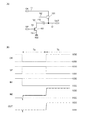
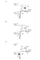
図16は、特許文献1において開示された駆動回路を示す。特許文献1の駆動回路は、トランジスタM1乃至トランジスタM7を有する。信号GOUT[N−1]がハイレベルになると、トランジスタM3がオンになる。すると、電圧VONがトランジスタM1のゲートに供給されるため、トランジスタM1のゲートの電位が上昇し始める。トランジスタM1のゲートの電位は徐々に上昇するため、トランジスタM3のゲートとソースとの間の電位差(以下、Vgsともいう)が徐々に小さくなる。やがて、トランジスタM3のVgsがトランジスタM3のしきい値電圧になり、トランジスタM3がオフになる。
FIG. 16 shows a drive circuit disclosed in
特許文献1の駆動回路では、トランジスタM1のゲートの電位の上昇に伴って、トランジスタM3のVgsが徐々に小さくなっていた。つまり、トランジスタM3のドレイン電流が徐々に小さくなっていた。よって、信号GOUT[N−1]がハイレベルになってからトランジスタM3がオフになるまでの時間が長くなっていた。一方で、信号CKVがハイレベルになる前にトランジスタM3をオフにして、トランジスタM1のゲートを浮遊状態にする必要があった。したがって、特許文献1の駆動回路では、駆動周波数を高くすることが困難であった。
In the drive circuit of
また、特許文献1の駆動回路では、トランジスタM1のゲートの電位を早く上昇させるために、トランジスタM3のW(W:チャネル幅)/L(L:チャネル長)比を大きくする必要があった。よって、トランジスタM3のサイズが大きくなり、レイアウト面積が大きくなっていた。
Further, in the driving circuit of
また、特許文献1の駆動回路では、トランジスタM1のゲートを浮遊状態にする必要があった。一方で、トランジスタM1のゲートにソース又はドレインが接続されるトランジスタのオフ電流によって、トランジスタM1のゲートから電荷が漏れていた。よって、トランジスタM1のゲートが浮遊状態になる期間を長くすることが困難であった。つまり、駆動周波数を低くすることが困難であった。
Further, in the drive circuit of
また、上述したとおり、特許文献1の駆動回路では、駆動周波数を高くすることも、低くすることも困難であったため、正常に動作する駆動周波数の範囲が狭くなっていた。
Further, as described above, in the drive circuit of
以上を鑑みて、本発明の一態様は、駆動周波数が高くても動作可能な駆動回路を提供することを課題の一とする。また、駆動周波数が低くても動作可能な駆動回路を提供することを課題の一とする。また、動作可能な駆動周波数の範囲が広い駆動回路を提供することを課題の一とする。また、トランジスタのW/L比を小さくすることを課題の一とする。また、新規の構成の回路を提供することを課題の一とする。なお、課題は効果と表裏一体の関係にあり、本明細書等で効果を述べる場合には、その効果に対応する課題が存在することは自明な事項である。一方で、本明細書等で課題を述べる場合には、その課題に対応する効果を奏することは自明な事項である。 In view of the above, an object of one embodiment of the present invention is to provide a driver circuit that can operate even when a driving frequency is high. Another object is to provide a driver circuit that can operate even at a low driving frequency. Another object is to provide a drive circuit with a wide range of operable drive frequencies. Another object is to reduce the W / L ratio of the transistor. Another object is to provide a circuit with a novel structure. It should be noted that the problem is in an integrated relationship with the effect, and when the effect is described in this specification and the like, it is obvious that there is a problem corresponding to the effect. On the other hand, when a problem is described in this specification and the like, it is obvious that an effect corresponding to the problem is achieved.
本発明の一態様は、ソース及びドレインの一方に第1の信号が入力される第1のトランジスタと、ソース及びドレインの一方に第1の電位が供給され、ゲートに第2の信号が入力される第2のトランジスタと、第1の電極が第1のトランジスタのソース及びドレインの他方と電気的に接続され、第2の電極が第2のトランジスタのソース及びドレインの他方と電気的に接続される容量素子と、を有する半導体装置である。そして、当該半導体装置は、第1の信号がロウレベルであり、第2の信号がハイレベルである第1の期間と、第1の信号がハイレベルであり、第2の信号がロウレベル又はハイレベルである第2の期間と、を有する。 In one embodiment of the present invention, a first transistor in which a first signal is input to one of a source and a drain, a first potential is supplied to one of the source and the drain, and a second signal is input to a gate The second transistor is electrically connected to the other of the source and the drain of the first transistor, and the second electrode is electrically connected to the other of the source and the drain of the second transistor. And a capacitor element. In the semiconductor device, the first period in which the first signal is low level and the second signal is high level, the first signal is high level, and the second signal is low level or high level. And a second period.
本発明の一態様は、ソース及びドレインの一方に第1の信号が入力される第1のトランジスタと、ソース及びドレインの一方に第1の電位が供給され、ゲートに第2の信号が入力される第2のトランジスタと、ソース及びドレインの一方に第1の信号が入力され、ゲートが第1のトランジスタのゲートと電気的に接続される第3のトランジスタと、第1の電極が第1のトランジスタのソース及びドレインの他方と電気的に接続され、第2の電極が第2のトランジスタのソース及びドレインの他方と電気的に接続される容量素子と、を有する半導体装置である。そして、当該半導体装置は、第1の信号がロウレベルであり、第2の信号がハイレベルである第1の期間と、第1の信号がハイレベルであり、第2の信号がロウレベル又はハイレベルである第2の期間と、を有する。 In one embodiment of the present invention, a first transistor in which a first signal is input to one of a source and a drain, a first potential is supplied to one of the source and the drain, and a second signal is input to a gate The second transistor, the third transistor whose first signal is input to one of the source and the drain, the gate of which is electrically connected to the gate of the first transistor, and the first electrode of which is the first transistor The semiconductor device includes a capacitor that is electrically connected to the other of the source and the drain of the transistor and whose second electrode is electrically connected to the other of the source and the drain of the second transistor. In the semiconductor device, the first period in which the first signal is low level and the second signal is high level, the first signal is high level, and the second signal is low level or high level. And a second period.
なお、上記本発明の一態様において、半導体装置は、ソース及びドレインの一方に第1の電位が供給され、ソース及びドレインの他方が第1のトランジスタのソース及びドレインの他方と電気的に接続され、ゲートが第2のトランジスタのソース及びドレインの他方と電気的に接続される第4のトランジスタと、ソース及びドレインの一方に第1の電位が供給され、ソース及びドレインの他方が第1のトランジスタのゲートと電気的に接続され、ゲートが第2のトランジスタのソース及びドレインの他方と電気的に接続される第5のトランジスタと、ソース及びドレインの一方に第2の電位が供給され、ソース及びドレインの他方が第2のトランジスタのソース及びドレインの他方と電気的に接続され、ゲートに第3の信号が入力される第6のトランジスタと、を有してもよい。 Note that in one embodiment of the present invention, in the semiconductor device, the first potential is supplied to one of the source and the drain, and the other of the source and the drain is electrically connected to the other of the source and the drain of the first transistor. A fourth transistor whose gate is electrically connected to the other of the source and the drain of the second transistor, a first potential supplied to one of the source and the drain, and the other of the source and the drain to the first transistor A second potential is supplied to one of the source and the drain; and a fifth transistor whose gate is electrically connected to the other of the source and the drain of the second transistor. The other of the drains is electrically connected to the other of the source and the drain of the second transistor, and the third signal is input to the gate. And the transistor may have.
なお、上記本発明の一態様において、第1のトランジスタのW(Wはチャネル幅)/L(Lはチャネル長)比は、第2のトランジスタのW/L比よりも大きくてもよい。 Note that in one embodiment of the present invention, the W (W is channel width) / L (L is channel length) ratio of the first transistor may be larger than the W / L ratio of the second transistor.
本発明の一態様は、駆動周波数が高くても動作可能な駆動回路を提供することができる。また、駆動周波数が低くても動作可能な駆動回路を提供することができる。また、動作可能な駆動周波数の範囲が広い駆動回路を提供することができる。また、トランジスタのW/L比を小さくすることができる。 One embodiment of the present invention can provide a driver circuit that can operate even when the driving frequency is high. In addition, a driving circuit that can operate even when the driving frequency is low can be provided. In addition, it is possible to provide a driving circuit with a wide range of operating driving frequencies. Further, the W / L ratio of the transistor can be reduced.
本発明を説明するための実施の形態の一例について、図面を用いて以下に説明する。なお、本発明の趣旨及びその範囲から逸脱することなく実施の形態の内容を変更することは、当業者であれば容易である。よって、本発明は、以下に示す実施の形態の記載内容に限定されない。 An example of an embodiment for explaining the present invention will be described below with reference to the drawings. Note that it is easy for those skilled in the art to change the contents of the embodiments without departing from the spirit and scope of the present invention. Therefore, the present invention is not limited to the description of the embodiments described below.
なお、本発明は、集積回路、RFタグ、表示装置など、トランジスタを用いたあらゆる半導体装置を、その範疇に含む。なお、集積回路には、マイクロプロセッサ、画像処理回路、DSP(Digital Signal Processor)、マイクロコントローラを含むLSI(Large Scale Integrated Circuit)、FPGA(Field Programmable Gate Array)やCPLD(Complex PLD)などのプログラマブル論理回路(PLD:Programmable Logic Device)が、その範疇に含まれる。また、表示装置には、液晶表示装置、有機発光素子(OLED)に代表される発光素子を各画素に備えた発光装置、電子ペーパー、DMD(Digital Micromirror Device)、PDP(Plasma Display Panel)、FED(Field Emission Display)などが、その範疇に含まれる。 Note that the present invention includes all semiconductor devices using transistors, such as an integrated circuit, an RF tag, and a display device. The integrated circuit includes a microprocessor, an image processing circuit, a DSP (Digital Signal Processor), an LSI (Large Scale Integrated Circuit) including a microcontroller, an FPGA (Field Programmable Gate Array), and a CPLD (Complex Programmable PLD). A circuit (PLD: Programmable Logic Device) is included in the category. In addition, the display device includes a liquid crystal display device, a light emitting device including a light emitting element represented by an organic light emitting element (OLED) in each pixel, electronic paper, DMD (Digital Micromirror Device), PDP (Plasma Display Panel), FED. (Field Emission Display) and the like are included in the category.
なお、本明細書において表示装置とは、液晶素子や発光素子などの表示素子が各画素に形成されたパネルと、該パネルにコントローラを含むIC等を実装した状態にあるモジュールとを、その範疇に含む。 Note that a display device in this specification includes a panel in which a display element such as a liquid crystal element or a light-emitting element is formed in each pixel, and a module in which an IC or the like including a controller is mounted on the panel. Included.
なお、本明細書において接続とは電気的な接続を意味しており、電流、電圧または電位が、供給可能、或いは伝送可能な状態に相当する。従って、接続している状態とは、直接接続している状態を必ずしも指すわけではなく、電流、電圧または電位が、供給可能、或いは伝送可能であるように、配線、抵抗、ダイオード、トランジスタなどの回路素子を介して間接的に接続している状態も、その範疇に含む。また、回路図上は独立している構成要素どうしが接続されている場合であっても、実際には、例えば配線の一部が電極として機能する場合など、一の導電膜が、複数の構成要素の機能を併せ持っている場合もある。本明細書において接続とは、このような、一の導電膜が、複数の構成要素の機能を併せ持っている場合も、その範疇に含める。 Note that in this specification, connection means electrical connection and corresponds to a state where current, voltage, or a potential can be supplied or transmitted. Therefore, the connected state does not necessarily indicate a directly connected state, and a wiring, a resistor, a diode, a transistor, or the like is provided so that current, voltage, or potential can be supplied or transmitted. The state of being indirectly connected through a circuit element is also included in the category. In addition, even when independent components on the circuit diagram are connected to each other, in practice, for example, when a part of the wiring functions as an electrode, one conductive film has a plurality of components. In some cases, it also has the function of an element. In this specification, the term “connection” includes a case where one conductive film has functions of a plurality of components.
なお、トランジスタのソースとは、活性層として機能する半導体膜の一部であるソース領域、或いは上記半導体膜に接続されたソース電極を意味する。同様に、トランジスタのドレインとは、上記半導体膜の一部であるドレイン領域、或いは上記半導体膜に接続されたドレイン電極を意味する。また、ゲートはゲート電極を意味する。 Note that the source of a transistor means a source region that is part of a semiconductor film functioning as an active layer or a source electrode connected to the semiconductor film. Similarly, a drain of a transistor means a drain region that is part of the semiconductor film or a drain electrode connected to the semiconductor film. The gate means a gate electrode.
なお、トランジスタが有するソースとドレインは、トランジスタの極性及び各端子に与えられる電位の高低によって、その呼び方が入れ替わる。一般的に、nチャネル型トランジスタでは、低い電位が与えられる端子がソースと呼ばれ、高い電位が与えられる端子がドレインと呼ばれる。また、pチャネル型トランジスタでは、低い電位が与えられる端子がドレインと呼ばれ、高い電位が与えられる端子がソースと呼ばれる。本明細書では、便宜上、ソースとドレインとが固定されているものと仮定して、トランジスタの接続関係を説明する場合があるが、実際には上記電位の関係に従ってソースとドレインの呼び方が入れ替わる。 Note that the terms “source” and “drain” of a transistor interchange with each other depending on the polarity of the transistor or the potential applied to each terminal. In general, in an n-channel transistor, a terminal to which a low potential is applied is called a source, and a terminal to which a high potential is applied is called a drain. In a p-channel transistor, a terminal to which a low potential is applied is called a drain, and a terminal to which a high potential is applied is called a source. In this specification, for the sake of convenience, the connection relationship between transistors may be described on the assumption that the source and the drain are fixed. However, the names of the source and the drain are actually switched according to the above-described potential relationship. .
(実施の形態1)
本実施の形態では、本発明の一態様に係る、基本回路、該基本回路を用いた順序回路、及び該順序回路を用いたシフトレジスタ回路について説明する。
(Embodiment 1)
In this embodiment, a basic circuit, a sequential circuit using the basic circuit, and a shift register circuit using the sequential circuit according to one embodiment of the present invention will be described.
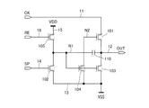
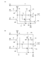
まず、本実施の形態の基本回路の構成について、図1(A)を参照して説明する。 First, the structure of the basic circuit of this embodiment is described with reference to FIG.
図1(A)の基本回路は、トランジスタ101、トランジスタ102、及び容量素子110を有する。
The basic circuit in FIG. 1A includes a
トランジスタ101の第1の端子は配線11と接続され、トランジスタ101の第2の端子は配線12と接続される。
A first terminal of the
トランジスタ102の第1の端子は配線13と接続され、トランジスタ102のゲートは配線14と接続される。
A first terminal of the
容量素子110の第1の電極(一方の電極ともいう)は配線12と接続され、容量素子110の第2の電極(他方の電極ともいう)はトランジスタ102の第2の端子と接続される。
A first electrode (also referred to as one electrode) of the
なお、トランジスタ102の第2の端子又は容量素子110の第2の電極をノードN1と示す。また、トランジスタ101のゲートをノードN2と示す。
Note that the second terminal of the
なお、トランジスタ101及びトランジスタ102は同一の導電型であることが好ましい。本実施の形態では、これらのトランジスタがNチャネル型である場合について説明する。
Note that the
なお、本明細書等において接続とは電気的な接続を意味しており、電流、電圧、電位、信号又は電荷等を供給又は伝送可能な状態に相当する。よって、「接続されている」とは、直接接続されている状態に加えて、例えば配線、導電膜、抵抗、ダイオード、トランジスタ、スイッチング素子などの素子を介して間接的に接続している状態も、その範疇に含む。 Note that in this specification and the like, connection means electrical connection and corresponds to a state in which current, voltage, potential, signal, charge, or the like can be supplied or transmitted. Thus, “connected” means not only a directly connected state but also an indirectly connected state via an element such as a wiring, a conductive film, a resistor, a diode, a transistor, or a switching element. Included in that category.
なお、トランジスタの第1の端子をトランジスタのソース及びドレインの一方、又はトランジスタの第1の電極ともいう。また、トランジスタの第2の端子をトランジスタのソース及びドレインの他方、又はトランジスタの第2の電極ともいう。 Note that the first terminal of the transistor is also referred to as one of a source and a drain of the transistor or a first electrode of the transistor. The second terminal of the transistor is also referred to as the other of the source and the drain of the transistor or the second electrode of the transistor.
配線11(信号線ともいう)には信号CKが入力されており、配線11は信号CKを伝達又は供給する機能を有する。信号CKはハイレベルとロウレベルとを有する信号である。また、信号CKはシフトレジスタ回路に入力される複数のクロック信号のいずれか一に対応する信号である。
A signal CK is input to the wiring 11 (also referred to as a signal line), and the
配線12(信号線ともいう)からは信号OUTが出力され、配線12は信号OUTを伝達又は供給する機能を有する。信号OUTはハイレベルとロウレベルとを有する信号である。また、信号OUTは、図1(A)の基本回路の出力信号である。また、信号OUTはシフトレジスタ回路から出力される複数の出力信号のいずれか一、又は順序回路の出力信号に対応する信号である。
A signal OUT is output from the wiring 12 (also referred to as a signal line), and the
配線13(電源線ともいう)には電位VSS(第1の電位ともいう)が供給され、配線13は電位VSSを伝達又は供給する機能を有する。電位VSSは一定の電位である。
A potential VSS (also referred to as a first potential) is supplied to the wiring 13 (also referred to as a power supply line), and the
配線14(信号線ともいう)には信号SPが入力され、配線14は信号SPを伝達又は供給する機能を有する。信号SPはハイレベルとロウレベルとを有する信号である。また、信号SPはトランジスタ102のオン又はオフを制御する信号である。また、信号SPはシフトレジスタ回路に入力されるスタートパルス、又は1段前若しくは複数段前の順序回路の出力信号等に対応する信号である。
A signal SP is input to the wiring 14 (also referred to as a signal line), and the
トランジスタ101は配線11と配線12との導通又は非導通を制御する機能を有する。また、トランジスタ101は配線11の信号CKを配線12に供給する機能を有する。また、トランジスタ101は配線12とノードN2との電位差を保持する機能を有する。
The
トランジスタ102は配線13とノードN1との導通又は非導通を制御する機能を有する。また、トランジスタ102は配線13の電位VSSをノードN1に供給する機能を有する。
The
容量素子110は配線12とノードN1との電位差を保持する機能を有する。
The
次に、図1(A)の基本回路の駆動方法について、図1(B)に示すタイミングチャート、及び図2を参照して説明する。 Next, a method for driving the basic circuit in FIG. 1A will be described with reference to a timing chart in FIG. 1B and FIG.
なお、信号CK及び信号SPのハイレベルの電位が電位VDD(第2の電位ともいう)であり、ロウレベルの電位が電位VSSであるとして説明する。なお、電位VDDは電位VSSよりも高い電位である。 Note that description is made assuming that the high-level potential of the signal CK and the signal SP is the potential VDD (also referred to as a second potential) and the low-level potential is the potential VSS. Note that the potential VDD is higher than the potential VSS.
また、ノードN1の初期の電位が電位VDDであり、ノードN2の初期の電位が電位VSSであり、配線12の初期の電位が電位VSSであると仮定して説明する。なお、ノードN2の初期の電位が電位VSSであれば、初期状態ではトランジスタ101がオフになっている。
Further, description will be made on the assumption that the initial potential of the node N1 is the potential VDD, the initial potential of the node N2 is the potential VSS, and the initial potential of the
また、便宜上、動作に必要な期間を期間Ta及び期間Tbに分けて説明する。 For convenience, the period necessary for the operation is divided into a period Ta and a period Tb.
まず、期間Taにおいて、信号SPがハイレベルになり、信号CKがロウレベルになる。信号SPがハイレベルになると、トランジスタ102がオンになる。トランジスタ102がオンになると、配線13の電位VSSがノードN1に供給される。よって、ノードN1の電位が電位VSSまで下降する。このとき、容量素子110がノードN1と配線12との電位差を保持しており、またトランジスタ101がオフになっているため、配線12が浮遊状態になっている。よって、ノードN1の電位の下降に伴って、配線12の電位が電位VSSから下降する。そして、配線12の電位がノードN2の電位(例えば電位VSS)からトランジスタ101の閾値電圧を引いた電位未満になれば、トランジスタ101がオンになる(図2(A)参照)。
First, in the period Ta, the signal SP becomes high level and the signal CK becomes low level. When the signal SP becomes high level, the
トランジスタ101がオンになると、配線11の信号CKが配線12に供給される。信号CKはロウレベルであるため、配線12の電位が電位VSSまで上昇する。このとき、トランジスタ101がノードN2と配線12との電位差を保持しており、またノードN2が浮遊状態になっている。よって、配線12の電位の上昇に伴って、ノードN2の電位が上昇する。ノードN2の電位が配線11の電位(例えば電位VSS)とトランジスタ101の閾値電圧とを足した電位を超えた電位になれば、トランジスタ101がオンのままになる。よって、配線12の電位が電位VSSまで上昇する。すなわち、信号OUTがロウレベルになる(図2(B)参照)。
When the
次に、期間Tbにおいて、信号SPがロウレベルになり、信号CKがハイレベルになる。信号SPがロウレベルになると、トランジスタ102がオフになる。また、上述したとおりトランジスタ101がオンのままになっている。よって、配線11の信号CKが配線12に供給されたままになる。信号CKはハイレベルであるため、配線12の電位が電位VSSから上昇する。このとき、トランジスタ101がノードN2と配線12との電位差を保持しており、またノードN2が浮遊状態のままになっている。よって、配線12の電位の上昇に伴って、ノードN2の電位も上昇する。ノードN2の電位が配線11の電位(例えば電位VDD)とトランジスタ101の閾値電圧とを足した電位を超えた電位になれば、トランジスタ101がオンのままになる。よって、配線12の電位が電位VDDまで上昇する。すなわち、信号OUTがハイレベルになる(図2(C)参照)。
Next, in the period Tb, the signal SP is at a low level and the signal CK is at a high level. When the signal SP becomes low level, the
図1(A)の基本回路では、期間Taにおいて、トランジスタ102のVgsを大きい電圧に維持することができるため、トランジスタ102のドレイン電流を大きい値に維持することができる。よって、ノードN1の電位を急速に下降させることができるため、期間Taを短くすることができる。つまり、駆動周波数を高くすることができる。
In the basic circuit in FIG. 1A, Vgs of the
また、トランジスタ102のVgsを大きい電圧に維持することができれば、トランジスタ102のW/L比を小さくすることができる。よって、レイアウト面積の縮小、入力容量の低減等を図ることができる。
In addition, if Vgs of the
なお、トランジスタ101のゲートと第2の端子との間に容量素子を接続してもよい。こうすれば、ノードN2と配線12との間の容量値を大きくすることができるため、ノードN2の電位をより高くすることができる。
Note that a capacitor may be connected between the gate of the
なお、期間Tbにおいても、信号SPがハイレベルのままであってもよい。こうすれば、期間Tbにおいて、トランジスタ102がオンのままになるため、配線13の電位VSSがノードN1に供給され続ける。よって、配線12の電位の変動に伴うノードN1の電位の変動を防止することができる。
Note that the signal SP may remain at a high level also during the period Tb. Thus, the
なお、期間Tbにおいて、信号SPが期間Taからハイレベルを維持した後にロウレベルとなってもよい。こうすれば、期間Tbにおいて、トランジスタ102がオンのままとなった後にオフとなるため、期間Tbのうち配線12の電位が変動している期間において、配線13の電位VSSがノードN1に供給され続ける。よって、配線12の電位の変動に伴うノードN1の電位の変動を防止することができる。
Note that in the period Tb, the signal SP may be at a low level after maintaining the high level from the period Ta. Thus, in the period Tb, the
なお、配線12に負荷が接続される場合、該負荷はトランジスタ101によって駆動される。よって、トランジスタ101のW/L比はトランジスタ102のW/L比よりも大きいことが好ましい。
Note that when a load is connected to the
なお、容量素子110として、トランジスタを用いてもよい。この場合、トランジスタのゲートをノードN1と接続し、トランジスタの第1の端子及び/又は第2の端子を配線12と接続することが好ましい。すなわち、容量素子110は、配線12と接続された半導体層と、ノードN1と接続されたゲート電極と、半導体層及びゲート電極の間のゲート絶縁層と、を有していてもよい。こうすれば、期間Taにおいて、ノードN1の電位が下降するときに、ノードN1と配線12との間の容量値を大きくすることができる。
Note that a transistor may be used as the
なお、トランジスタ102を、第1の端子が配線13と接続され、第2の端子がノードN1と接続されるスイッチング素子に置き換えてもよい。
Note that the
なお、信号SPのハイレベルの電位は電位VDDよりも低くてもよい。こうすれば、信号SPの振幅電圧を小さくすることができるため、消費電力の削減を図ることができる。 Note that the high-level potential of the signal SP may be lower than the potential VDD. In this way, the amplitude voltage of the signal SP can be reduced, so that power consumption can be reduced.
なお、信号SPのロウレベルの電位は電位VSSよりも低くてもよい。こうすれば、トランジスタ102がノーマリーオンであってもトランジスタ102を確実にオフにすることができる。
Note that the low-level potential of the signal SP may be lower than the potential VSS. Thus, the
次に、図1(A)の基本回路を用いた順序回路について説明する。 Next, a sequential circuit using the basic circuit in FIG.
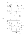
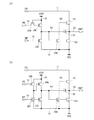
まず、本実施の形態の順序回路の構成について、図3を参照して説明する。図3の順序回路は、図1(A)の基本回路にトランジスタ103乃至トランジスタ105を設けた構成である。
First, the structure of the sequential circuit of this embodiment will be described with reference to FIG. The sequential circuit in FIG. 3 has a structure in which the
なお、トランジスタ101乃至トランジスタ105は同一の導電型であることが好ましい。本実施の形態では、これらのトランジスタがNチャネル型である場合について説明する。
Note that the
トランジスタ103の第1の端子は配線13と接続され、トランジスタ103の第2の端子は配線12と接続され、トランジスタ103のゲートはノードN1と接続される。
A first terminal of the
トランジスタ104の第1の端子は配線13と接続され、トランジスタ104の第2の端子はノードN2と接続され、トランジスタ104のゲートはノードN1と接続される。
A first terminal of the
トランジスタ105の第1の端子は配線15と接続され、トランジスタ105の第2の端子はノードN1と接続され、トランジスタ105のゲートは配線16と接続される。
A first terminal of the
配線15(電源線ともいう)には電位VDDが供給され、配線15は電位VDDを伝達又は供給する機能を有する。
A potential VDD is supplied to the wiring 15 (also referred to as a power supply line), and the
配線16(信号線ともいう)には信号REが入力されており、配線16は信号REを伝達又は供給する機能を有する。信号REはハイレベルとロウレベルとを有する信号である。また、信号REはトランジスタ105のオン又はオフを制御する信号である。また、信号REはシフトレジスタ回路に入力されるリセットパルス、又は1段後若しくは複数段後の順序回路の出力信号等に対応する信号である。
A signal RE is input to the wiring 16 (also referred to as a signal line), and the
トランジスタ103は配線13と配線12との導通又は非導通を制御する機能を有する。また、トランジスタ103は配線13の電位VSSを配線12に供給する機能を有する。
The
トランジスタ104は配線13とノードN2との導通又は非導通を制御する機能を有する。また、トランジスタ104は配線13の電位VSSをノードN2に供給する機能を有する。
The
トランジスタ105は配線15とノードN1との導通又は非導通を制御する機能を有する。また、トランジスタ105は配線15の電位VDDをノードN1に供給する機能を有する。
The
次に、図3の順序回路の動作について、図4のタイミングチャートを参照して説明する。 Next, the operation of the sequential circuit in FIG. 3 will be described with reference to the timing chart in FIG.
なお、信号CK、信号SP及び信号REのハイレベルの電位が電位VDDであり、ロウレベルの電位が電位VSSであるとして説明する。 Note that the high-level potentials of the signal CK, the signal SP, and the signal RE are the potential VDD, and the low-level potential is the potential VSS.
また、ノードN1の初期の電位が電位VDDであり、ノードN2の初期の電位が電位VSSであり、配線12の初期の電位が電位VSSであるとして説明する。なお、ノードN2の初期の電位が電位VSSであるため、初期状態ではトランジスタ101がオフになっている。
Further, description is made on the assumption that the initial potential of the node N1 is the potential VDD, the initial potential of the node N2 is the potential VSS, and the initial potential of the
また、便宜上、動作に必要な期間を期間Ta、期間Tb、期間Tc及び期間Tdに分けて説明する。 For convenience, the period required for the operation is divided into a period Ta, a period Tb, a period Tc, and a period Td.
まず、期間Taにおいて、信号SPがハイレベルになり、信号REがロウレベルになり、信号CKがロウレベルになる。信号REがロウレベルになると、トランジスタ105がオフになる。また、信号SPがハイレベルになると、トランジスタ102がオンになる。トランジスタ102がオンになると、配線13の電位VSSがノードN1に供給される。よって、ノードN1の電位が電位VSSまで下降する。ノードN1の電位が下降すると、トランジスタ103及びトランジスタ104がオフになる。トランジスタ104がオフになると、ノードN2が浮遊状態になる。よって、ノードN2の電位が電位VSSに維持されるため、トランジスタ101がオフのままになる。
First, in the period Ta, the signal SP becomes high level, the signal RE becomes low level, and the signal CK becomes low level. When the signal RE becomes low level, the
ここで、ノードN1の電位が下降しているとき、容量素子110がノードN1と配線12との電位差を保持しており、またトランジスタ101及びトランジスタ103がオフになっているため、配線12が浮遊状態になっている。よって、ノードN1の電位の下降に伴って、配線12の電位が電位VSSから下降する。配線12の電位がノードN2の電位(例えば電位VSS)からトランジスタ101の閾値電圧を引いた電位未満になれば、トランジスタ101がオンになる。トランジスタ101がオンになると、配線11の信号CKが配線12に供給される。信号CKはロウレベルであるため、配線12の電位が上昇する。このとき、トランジスタ101がノードN2と配線12との電位差を保持しており、またトランジスタ104がオフになっているため、ノードN2が浮遊状態になっている。よって、配線12の電位の上昇に伴って、ノードN2の電位が上昇する。ノードN2の電位が配線11の電位(例えば電位VSS)とトランジスタ101の閾値電圧とを足した電位を超えた電位になれば、トランジスタ101がオンのままになる。よって、配線12の電位が電位VSSまで上昇する。すなわち、信号OUTがロウレベルになる。
Here, when the potential of the node N1 is decreasing, the
次に、期間Tbにおいて、信号SPがロウレベルになり、信号REがロウレベルのままになり、信号CKがハイレベルになる。信号REがロウレベルのままなので、トランジスタ105がオフのままになる。また、信号SPがロウレベルになるため、トランジスタ102がオフになる。よって、ノードN1が浮遊状態になり、ノードN1の電位が期間Taにおける電位に維持されるため、トランジスタ103及びトランジスタ104がオフのままになる。
Next, in the period Tb, the signal SP becomes low level, the signal RE remains low level, and the signal CK becomes high level. Since the signal RE remains at a low level, the
ここで、トランジスタ101がオンのままになっているため、配線11の信号CKが配線12に供給されたままになっている。信号CKはハイレベルであるため、配線11の電位が上昇する。このとき、トランジスタ101がノードN2と配線12との間の電位差を保持しており、またトランジスタ104がオフであるため、ノードN2が浮遊状態になっている。よって、配線12の電位の上昇に伴って、ノードN2の電位が上昇する。ノードN2の電位が配線11の電位(例えば電位VDD)とトランジスタ101の閾値電圧とを足した電位を超えた電位になれば、トランジスタ101がオンのままになる。よって、配線12の電位が電位VDDまで上昇する。すなわち、信号OUTがハイレベルになる。
Here, since the
次に、期間Tcにおいて、信号SPがロウレベルのままになり、信号REがハイレベルになり、信号CKがロウレベルになる。信号SPがロウレベルのままになるため、トランジスタ102がオフのままになる。また、信号REがハイレベルになるため、トランジスタ105がオンになる。トランジスタ105がオンになると、配線15の電位VDDがノードN1に供給されるため、ノードN1の電位が上昇する。やがて、ノードN1の電位がトランジスタ105のゲートの電位(例えば電位VDD)からトランジスタ105の閾値電圧を引いた電位まで上昇すると、トランジスタ105がオフになる。よって、ノードN1が浮遊状態になり、ノードN1の電位が高い電位に維持される。また、ノードN1の電位が上昇すると、トランジスタ103及びトランジスタ104がオンになる。トランジスタ104がオンになると、配線13の電位VSSがノードN2に供給される。よって、ノードN2の電位が電位VSSまで下降する。ノードN2の電位が電位VSSまで下降すると、トランジスタ101がオフになる。また、トランジスタ103がオンになると、配線13の電位VSSが配線12に供給される。よって、配線12の電位が電位VSSまで下降する。つまり、信号OUTがロウレベルになる。
Next, in the period Tc, the signal SP remains at low level, the signal RE becomes high level, and the signal CK becomes low level. Since the signal SP remains at a low level, the
次に、期間Tdにおいて、信号SPがロウレベルのままになり、信号REがロウレベルになり、信号CKがハイレベルとロウレベルとを繰り返す。信号SPがロウレベルのままになるため、トランジスタ102がオフのままになる。また、信号REがロウレベルになるため、トランジスタ105がオフのままになる。トランジスタ102及びトランジスタ105がオフのままなので、ノードN1が浮遊状態のままになる。よって、ノードN1の電位が期間Tcにおける電位に維持されるため、トランジスタ103及びトランジスタ104がオンのままになる。トランジスタ104がオンのままになると、配線13の電位VSSがノードN2に供給されたままになる。よって、ノードN2の電位が電位VSSのままになり、トランジスタ101がオフのままになる。また、トランジスタ103がオンのままになると、配線13の電位VSSが配線12に供給されたままになる。よって、配線12の電位が電位VSSのままになる。つまり、信号OUTがロウレベルのままになる。
Next, in the period Td, the signal SP remains at low level, the signal RE becomes low level, and the signal CK repeats high level and low level. Since the signal SP remains at a low level, the
図3の順序回路では、期間Taにおいて、配線12の電位が電位VSS未満となるため、トランジスタ103のソースとドレインを反転させることができる。よって、トランジスタ103の劣化を抑制することができる。
In the sequential circuit in FIG. 3, since the potential of the
また、図3の順序回路は、上述した基本回路と同様の効果を奏することができる。 Further, the sequential circuit of FIG. 3 can achieve the same effects as the basic circuit described above.
なお、配線12に負荷が接続される場合、該負荷はトランジスタ101及びトランジスタ103によって駆動される。よって、トランジスタ101のW/L比はトランジスタ102、トランジスタ104及びトランジスタ105のW/L比よりも大きいことが好ましい。また、トランジスタ103のW/L比はトランジスタ102、トランジスタ104及びトランジスタ105のW/L比よりも大きいことが好ましい。
Note that when a load is connected to the
なお、トランジスタ101及びトランジスタ103は共に配線12に電荷を供給する。ただし、期間Tbにおけるトランジスタ101のVgsは期間Tcにおけるトランジスタ103のVgsよりも小さいことが多い。よって、トランジスタ101のW/L比はトランジスタ103のW/L比よりも大きいことが好ましい。
Note that both the
なお、トランジスタ102及びトランジスタ105は共にノードN1に電荷を供給する。ただし、期間Taにおけるトランジスタ102のVgsが大きい値に維持されるのに対し、期間Tcにおけるトランジスタ105のVgsは徐々に小さくなる。よって、トランジスタ105のW/L比はトランジスタ102のW/L比よりも大きいことが好ましい。
Note that both the
なお、トランジスタ102のW/L比はトランジスタ104のW/L比よりも大きいことが好ましい。
Note that the W / L ratio of the
なお、信号REのハイレベルの電位は電位VDDよりも高くてもよい。こうすれば、期間Tcにおいて、トランジスタ105がオフになることを防止することができるため、ノードN1の電位を電位VDDまで上昇させることができる。
Note that the high-level potential of the signal RE may be higher than the potential VDD. Thus, the
なお、信号REのロウレベルの電位は電位VSSよりも低くてもよい。こうすれば、トランジスタ105がノーマリーオンであってもトランジスタ105を確実にオフにすることができる。
Note that the low-level potential of the signal RE may be lower than the potential VSS. Thus, the
なお、配線15には、電位VDDよりも低い電位を供給してもよい。
Note that a potential lower than the potential VDD may be supplied to the
なお、トランジスタ103を、第1の端子が配線13と接続され、第2の端子が配線12と接続されるスイッチング素子に置き換えてもよい。
Note that the
なお、トランジスタ104を、第1の端子が配線13と接続され、第2の端子がノードN2と接続されるスイッチング素子に置き換えてもよい。
Note that the
なお、トランジスタ105を、第1の端子が配線15と接続され、第2の端子がノードN1と接続されるスイッチング素子に置き換えてもよい。
Note that the
次に、図3の順序回路を用いたシフトレジスタ回路について説明する。 Next, a shift register circuit using the sequential circuit in FIG. 3 will be described.
まず、本実施の形態のシフトレジスタ回路の構成について、図5を参照して説明する。図5のシフトレジスタ回路は、N(Nは自然数)段の順序回路100を有する。ただし、図5では、便宜上、N段の順序回路100のうち1段目乃至3段目の順序回路100(順序回路100[1]乃至順序回路100[3]と示す)のみを示す。
First, the structure of the shift register circuit of this embodiment is described with reference to FIG. The shift register circuit in FIG. 5 includes a
シフトレジスタ回路は、N本の配線21(配線21[1]乃至配線21[N]と示す)、配線22、配線23及び配線24と接続される。具体的には、i(iは2〜N−1のいずれか一)段目の順序回路100において、トランジスタ101の第1の端子が配線22又は配線23と接続され、トランジスタ101の第2の端子が配線21[i]と接続され、トランジスタ102のゲートが配線21[i−1]と接続され、トランジスタ105のゲートが配線21[i+1]と接続される。
The shift register circuit is connected to N wirings 21 (shown as wirings 21 [1] to 21 [N]), a
また、1段目の順序回路100の接続関係はi段目の順序回路100の接続関係と同様であるが、前段に順序回路100が設けられていないため、トランジスタ102のゲートの接続先がない。そこで、1段目の順序回路100では、トランジスタ102のゲートが配線24と接続される。
The connection relationship of the
また、N段目の順序回路100の接続関係はi段目の順序回路100の接続関係と同様であるが、後段に順序回路100が設けられていないため、トランジスタ105のゲートの接続先がない。そこで、N段目の順序回路100では、トランジスタ105のゲートが配線24と接続される。ただし、N段目の順序回路100において、トランジスタ105のゲートを、リセットパルスが入力される配線、N段目の順序回路100の後段に設けたダミー回路の出力等と接続してもよい。
The connection relationship of the
なお、奇数段目の順序回路100において、トランジスタ101の第1の端子が配線22及び配線23の一方と接続される場合、偶数段目の順序回路100においては、トランジスタ101の第1の端子が配線22及び配線23の他方と接続される。
Note that in the odd-numbered
配線21(信号線ともいう)からは信号SOUTが出力されており、配線21は信号SOUTを伝達又は供給する機能を有する。なお、i段目の順序回路100においては、i本目の配線21は配線12に対応する配線であり、i−1本目の配線21は配線14に対応する配線であり、i+1本目の配線21は配線16に対応する配線である。また、i本目の配線21から出力される信号SOUTは信号OUTに対応する信号であり、i−1本目の配線21から出力される信号SOUTは信号SPに対応する信号であり、i+1本目の配線21から出力される信号SOUTは信号REに対応する信号である。
A signal SOUT is output from the wiring 21 (also referred to as a signal line), and the
配線22(信号線ともいう)には信号SCKが入力されており、配線22は信号SCKを伝達又は供給する機能を有する。なお、奇数段目及び偶数段目の一方の順序回路100においては、配線22は配線11に対応する配線であり、信号SCKは信号CKに対応する信号である。
A signal SCK is input to the wiring 22 (also referred to as a signal line), and the
配線23(信号線ともいう)には信号SCKBが入力されており、配線23は信号SCKBを伝達又は供給する機能を有する。なお、奇数段目及び偶数段目の他方の順序回路100においては、配線23は配線11に対応する配線であり、信号SCKBは信号CKに対応する信号である。なお、信号SCKBは、信号SCKの反転信号、又は信号SCKから位相がずれた信号である。
A signal SCKB is input to the wiring 23 (also referred to as a signal line), and the
配線24(信号線ともいう)には信号SSPが入力されており、配線24は信号SSPを伝達又は供給する機能を有する。なお、1段目の順序回路100においては、配線24は配線14に対応する配線であり、信号SSPは信号SPに対応する配線である。
A signal SSP is input to the wiring 24 (also referred to as a signal line), and the
図5のシフトレジスタ回路は、上述した基本回路又は順序回路と同様の効果を奏することができる。 The shift register circuit in FIG. 5 can achieve the same effects as the basic circuit or the sequential circuit described above.
なお、i段目の順序回路100において、トランジスタ102のゲートをi−2本目の配線21又はi−3本目の配線21と接続してもよい。
Note that in the i-th
なお、i段目の順序回路100において、トランジスタ105のゲートをi+2本目の配線21又はi+3本目の配線21と接続してもよい。
Note that in the i-th
本実施の形態は、他の実施の形態等と適宜組み合わせて実施することが可能である。 This embodiment can be implemented in combination with any of the other embodiments as appropriate.
(実施の形態2)
本実施の形態では、バッファ回路を設けた基本回路、及び該基本回路を用いた順序回路について説明する。
(Embodiment 2)
In this embodiment, a basic circuit provided with a buffer circuit and a sequential circuit using the basic circuit will be described.
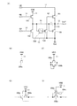
まず、本実施の形態の基本回路の構成について、図6(A)を参照して説明する。図6(A)の基本回路は、図1(A)の基本回路にトランジスタ201を設けた構成である。
First, the structure of the basic circuit of this embodiment is described with reference to FIG. The basic circuit in FIG. 6A has a structure in which a
なお、トランジスタ201はトランジスタ101と同一の導電型であることが好ましい。本実施の形態では、これらのトランジスタがNチャネル型である場合について説明する。
Note that the
トランジスタ201の第1の端子は配線11と接続され、トランジスタ201の第2の端子は配線31と接続され、トランジスタ201のゲートはトランジスタ101のゲートと接続される。
A first terminal of the
トランジスタ201は配線11と配線31との導通又は非導通を制御する機能を有する。また、トランジスタ201は配線11の信号CKを配線31に供給する機能を有する。また、トランジスタ201は配線31とノードN2との電位差を保持する機能を有する。
The
配線31(信号線ともいう)からは信号BOUTが出力され、配線31は信号BOUTを伝達又は供給する機能を有する。信号BOUTはハイレベルとロウレベルとを有する信号である。また、信号BOUTは、図6(A)の基本回路の出力信号である。また、信号BOUTはシフトレジスタ回路から出力される複数の出力信号のいずれか一、又は順序回路の出力信号に対応する信号である。
A signal BOUT is output from the wiring 31 (also referred to as a signal line), and the
次に、図6(A)の基本回路の駆動方法について説明する。 Next, a method for driving the basic circuit in FIG.
なお、図1(A)の基本回路の駆動方法と共通するところはその説明を省略する。 Note that description of portions common to the driving method of the basic circuit in FIG.
また、配線31の初期の電位が電位VSSであるとして説明する。
Further, description is made assuming that the initial potential of the
また、便宜上、ノードN2の電位がトランジスタ101がオンになる電位となれば、トランジスタ201もオンになるものとして説明する。
For the sake of convenience, description will be made assuming that the
まず、期間Taでは、ノードN2の電位が配線11の電位(例えば電位VSS)とトランジスタ101の閾値電圧とを足した電位を超えた電位になる。よって、トランジスタ201がオンになるため、配線11の信号CKが配線31に供給される。信号CKはロウレベルであるため、配線31の電位が電位VSSのままになる。すなわち、信号BOUTがロウレベルとなる。
First, in the period Ta, the potential of the node N2 is higher than the potential obtained by adding the potential of the wiring 11 (for example, the potential VSS) and the threshold voltage of the
次に、期間Tbでは、ノードN2の電位が配線11の電位(例えば電位VDD)とトランジスタ101の閾値電圧とを足した電位を超えた電位になる。よって、トランジスタ201がオンのままになるため、配線11の信号CKが配線31に供給されたままになる。信号CKがハイレベルであるため、配線31の電位が電位VDDまで上昇する。すなわち、信号BOUTがハイレベルになる。
Next, in the period Tb, the potential of the node N2 exceeds the potential obtained by adding the potential of the wiring 11 (eg, the potential VDD) and the threshold voltage of the
図6(A)の基本回路では、信号SPがハイレベルになる期間において、配線31の電位が電位VSSから下降することを防止することができる。よって、図6(A)の基本回路は、より安定した信号を出力することができる。
In the basic circuit in FIG. 6A, the potential of the
また、図6(A)の基本回路は、実施の形態1の基本回路と同様の効果を奏することができる。
In addition, the basic circuit in FIG. 6A can achieve the same effects as the basic circuit in
なお、配線31に負荷が接続される場合、該負荷はトランジスタ201によって駆動される。また、配線31に接続される負荷は配線12に接続される負荷よりも大きいことが多い。よって、トランジスタ201のW/L比はトランジスタ101のW/L比よりも大きいことが好ましい。
Note that when a load is connected to the
なお、トランジスタ101の第1の端子とトランジスタ201の第1の端子とを異なる配線と接続してもよい。
Note that the first terminal of the
次に、図6(A)の基本回路を用いた順序回路について説明する。 Next, a sequential circuit using the basic circuit in FIG.
まず、本実施の形態の順序回路の構成について、図6(B)を参照して説明する。図6(B)の順序回路は、図3の順序回路にトランジスタ201及びトランジスタ202を設けた構成である。
First, the structure of the sequential circuit of this embodiment is described with reference to FIG. The sequential circuit in FIG. 6B has a structure in which the
なお、トランジスタ201及びトランジスタ202はトランジスタ101と同じ導電型であることが好ましい。本実施の形態では、これらのトランジスタがNチャネル型である場合について説明する。
Note that the
トランジスタ201の第1の端子は配線11と接続され、トランジスタ201の第2の端子は配線31と接続され、トランジスタ201のゲートはトランジスタ101のゲートと接続される。
A first terminal of the
トランジスタ202の第1の端子は配線13と接続され、トランジスタ202の第2の端子は配線31と接続され、トランジスタ202のゲートはノードN1と接続される。
A first terminal of the
トランジスタ202は配線13と配線31との導通又は非導通を制御する機能を有する。また、トランジスタ202は配線13の電位VSSを配線31に供給する機能を有する。
The
次に、図6(B)の順序回路の駆動方法について説明する。 Next, a method for driving the sequential circuit in FIG. 6B is described.
なお、図3の順序回路の駆動方法と共通するところはその説明を省略する。 Note that a description of the common method with the driving method of the sequential circuit in FIG. 3 is omitted.
また、配線31の初期の電位VSSであるとして説明する。
Further, description will be made assuming that the potential is the initial potential VSS of the
また、便宜上、ノードN2の電位がトランジスタ101がオンになる電位となれば、トランジスタ201もオンになるものとして説明する。
For the sake of convenience, description will be made assuming that the
また、便宜上、ノードN1の電位がトランジスタ103がオンになる電位となれば、トランジスタ202もオンになるものとして説明する。
For convenience, the description is made on the assumption that the
まず、期間Taにおいて、ノードN1の電位が電位VSSとなるため、トランジスタ202がオフになる。また、ノードN2の電位が配線11の電位(例えば電位VSS)とトランジスタ101の閾値電圧とを足した電位を超えた電位になる。よって、トランジスタ201がオンになるため、配線11の信号CKが配線31に供給される。信号CKはロウレベルであるため、配線31の電位が電位VSSのままになる。すなわち、信号BOUTがロウレベルとなる。
First, in the period Ta, the potential of the node N1 becomes the potential VSS, so that the
次に、期間Tbにおいて、ノードN1の電位が期間Taにおける電位に維持されるため、トランジスタ202がオフのままになる。また、ノードN2の電位が配線11の電位(例えば電位VDD)とトランジスタ101の閾値電圧とを足した電位を超えた電位になる。よって、トランジスタ201がオンになるため、配線11の信号CKが配線31に供給されたままになる。信号CKがハイレベルであるため、配線31の電位が電位VDDまで上昇する。すなわち、信号BOUTがハイレベルになる。
Next, in the period Tb, the potential of the node N1 is maintained at the potential in the period Ta, so that the
次に、期間Tcにおいて、ノードN2の電位が電位VSSになるため、トランジスタ201がオフになる。また、ノードN1の電位が上昇し、トランジスタ105のゲートの電位(例えば電位VDD)からトランジスタ105の閾値電圧を引いた電位となる。よって、トランジスタ202がオンになるため、配線13の電位が配線31に供給される。よって、配線31の電位が電位VSSまで下降する。つまり、信号BOUTがロウレベルになる。
Next, in the period Tc, since the potential of the node N2 becomes the potential VSS, the
次に、期間Tdにおいて、ノードN2の電位が電位VSSのままになるため、トランジスタ201がオフのままになる。また、ノードN1の電位が期間Tcにおける電位に維持される。よって、トランジスタ202がオンのままになるため、配線13の電位が配線31に供給されたままになる。そのため、配線31の電位が電位VSSのままになる。つまり、信号BOUTがロウレベルのままになる。
Next, in the period Td, the potential of the node N2 remains at the potential VSS, so that the
図6(B)の順序回路は、上述した基本回路、実施の形態1の基本回路及び順序回路と同様の効果を奏することができる。
The sequential circuit in FIG. 6B can achieve the same effects as the basic circuit described above, the basic circuit in
なお、配線31に負荷が接続される場合、該負荷はトランジスタ201によって駆動される。また、配線31に接続される負荷は配線12に接続される負荷よりも大きいことが多い。よって、トランジスタ202のW/L比はトランジスタ103のW/L比よりも大きいことが好ましい。
Note that when a load is connected to the
なお、トランジスタ201及びトランジスタ202は共に配線31に電荷を供給する。ただし、期間Tbにおけるトランジスタ201のVgsは期間Tcにおけるトランジスタ202のVgsよりも小さいことが多い。よって、トランジスタ201のW/L比はトランジスタ202のW/L比よりも大きいことが好ましい。
Note that both the
なお、トランジスタ202を、第1の端子が配線13と接続され、第2の端子が配線31と接続されるスイッチング素子に置き換えてもよい。
Note that the
本実施の形態は、他の実施の形態等と適宜組み合わせて実施することが可能である。 This embodiment can be implemented in combination with any of the other embodiments as appropriate.
(実施の形態3)
本実施の形態では、実施の形態1及び実施の形態2とは異なる順序回路について説明する。
(Embodiment 3)
In this embodiment, a sequential circuit different from those in
まず、図7(A)の順序回路は、図3の順序回路において、トランジスタ105の第2の端子を配線16と接続した構成である。
First, the sequential circuit in FIG. 7A has a structure in which the second terminal of the
図7(A)の順序回路では、配線15及び電位VDDを省略することができる。
In the sequential circuit in FIG. 7A, the
なお、実施の形態1〜2で述べた順序回路及びシフトレジスタ回路等においても、トランジスタ105の第2の端子を配線16と接続してもよい。
Note that in the sequential circuit, the shift register circuit, and the like described in
次に、図7(B)の順序回路は、図3の順序回路において、トランジスタ105の第2の端子を配線17と接続した構成である。
Next, the sequential circuit in FIG. 7B has a structure in which the second terminal of the
配線17(信号線ともいう)には信号CKBが入力されており、配線17は信号CKBを伝達又は供給する機能を有する。信号CKBはハイレベルとロウレベルとを有する信号である。また、信号CKBはシフトレジスタ回路に入力される複数のクロック信号のいずれか一に対応する信号である。また、信号CKBは、信号CKの反転信号、又は信号CKから位相がずれた信号である。
A signal CKB is input to the wiring 17 (also referred to as a signal line), and the
図7(B)の順序回路では、配線15及び電位VDDを省略することができる。
In the sequential circuit in FIG. 7B, the
なお、実施の形態1〜2で述べた順序回路及びシフトレジスタ回路等においても、トランジスタ105の第2の端子を配線17と接続してもよい。
Note that in the sequential circuit, the shift register circuit, and the like described in
次に、図8(A)の順序回路は、図3の順序回路に、容量素子301を設けた構成である。
Next, the sequential circuit in FIG. 8A has a structure in which the
容量素子301の第1の電極は配線13と接続され、容量素子301の第2の電極はノードN1と接続される。
A first electrode of the
容量素子301は配線13とノードN1との電位差を保持する機能を有する。また、容量素子301はノードN1の電位を維持する機能を有する。
The
期間Taにおいて、容量素子301は、配線13の電位VSSがノードN1に供給されるときの配線13とノードN1との電位差を保持する。
In the period Ta, the
期間Tbにおいて、容量素子301は、期間Taにおける電圧を保持する。
In the period Tb, the
期間Tcにおいて、容量素子301は、配線15の電位VDDがノードN1に供給されるときの配線13とノードN1との電位差を保持する。
In the period Tc, the
期間Tdにおいて、容量素子301は、期間Tcにおける電圧を保持する。
In the period Td, the
図8(A)の順序回路では、期間Tbにおいて、容量素子301が配線13とノードN1との電位差を保持しているため、配線12の電位の上昇に伴うノードN1の電位の上昇を抑制することができる。
In the sequential circuit in FIG. 8A, since the
また、期間Tdにおいて、容量素子301が配線13とノードN1との電位差を保持しているため、ノードN1の電位の変動を抑制することができる。
Further, since the
なお、容量素子301の第1の電極の接続先は配線13に限定されない。例えば、容量素子301の第1の電極を配線11、配線14、配線15、又は配線16等と接続してもよい。
Note that the connection destination of the first electrode of the
なお、実施の形態1〜2及び本実施の形態で述べた基本回路、順序回路及びシフトレジスタ回路等においても、容量素子301を設けてもよい。
Note that the
次に、図8(B)の順序回路は、図3の順序回路に、トランジスタ302を設けた構成である。
Next, the sequential circuit in FIG. 8B has a structure in which the
なお、トランジスタ302はトランジスタ101と同じ導電型であることが好ましい。本実施の形態では、これらのトランジスタがNチャネル型である場合について説明する。
Note that the
トランジスタ302の第1の端子は配線13と接続され、トランジスタ302の第2の端子はノードN2と接続され、トランジスタ302のゲートは配線16と接続される。
A first terminal of the
トランジスタ302は配線13とノードN2との導通又は非導通を制御する機能を有する。また、トランジスタ302は配線13の電位VSSをノードN2に供給する機能を有する。
The
期間Ta、期間Tb及び期間Tdにおいて、信号REはロウレベルになる。よって、トランジスタ302はオフになる。
In the period Ta, the period Tb, and the period Td, the signal RE is at a low level. Thus, the
期間Tcにおいて、信号REはハイレベルになる。信号REがハイレベルになると、トランジスタ302がオンになり、配線13の電位VSSがノードN2に供給される。
In the period Tc, the signal RE becomes a high level. When the signal RE becomes a high level, the
図8(B)の順序回路では、トランジスタ302を有することにより、期間Tcにおいて、配線13の電位VSSをノードN2に供給するタイミングを早くすることができる。よって、ノードN2の電位が下降するタイミングを早くすることができるため、トランジスタ101がオフになるタイミングを早くすることができる。
In the sequential circuit in FIG. 8B, the
なお、実施の形態1〜2及び本実施の形態で述べた基本回路、順序回路及びシフトレジスタ回路等においても、トランジスタ302を設けてもよい。
Note that the
なお、トランジスタ302を第1の端子が配線13と接続され、第2の端子がノードN2と接続されるスイッチング素子に置き換えてもよい。
Note that the
次に、図9(A)の順序回路は、図3の順序回路に、トランジスタ303を設けた構成である。
Next, the sequential circuit in FIG. 9A has a structure in which the
トランジスタ303の第1の端子は配線13と接続され、トランジスタ303の第2の端子は配線12と接続され、トランジスタ303のゲートは配線16と接続される。
A first terminal of the
なお、トランジスタ303はトランジスタ101と同じ導電型であることが好ましい。本実施の形態では、これらのトランジスタがNチャネル型である場合について説明する。
Note that the
トランジスタ303は配線13と配線12との導通又は非導通を制御する機能を有する。また、トランジスタ303は配線13の電位VSSを配線12に供給する機能を有する。
The
期間Ta、期間Tb及び期間Tdにおいて、信号REはロウレベルになる。よって、トランジスタ303はオフになる。
In the period Ta, the period Tb, and the period Td, the signal RE is at a low level. Thus, the
期間Tcにおいて、信号REはハイレベルになる。信号REがハイレベルになると、トランジスタ303がオンになり、配線13の電位VSSが配線12に供給される。
In the period Tc, the signal RE becomes a high level. When the signal RE is at a high level, the
図9(A)の順序回路では、トランジスタ303を有することにより、期間Tcにおいて、配線13の電位VSSを配線12に供給するタイミングを早くすることができる。よって、信号OUTの立ち下がり時間を短くすることができる。
In the sequential circuit in FIG. 9A, the
なお、実施の形態1〜2及び本実施の形態で述べた基本回路、順序回路及びシフトレジスタ回路等においても、トランジスタ303を設けてもよい。
Note that the
特に、実施の形態2で述べた基本回路及び順序回路等において、トランジスタ303を設ける場合には、トランジスタ303の第2の端子を配線31と接続してもよい。または、トランジスタ303を設け、さらに第1の端子が配線13と接続され、第2の端子が配線31と接続され、ゲートが配線16と接続されたトランジスタを設けてもよい。こうすれば、信号BOUTの立ち下がり時間を短くすることができる。
In particular, when the
なお、トランジスタ303を第1の端子が配線13と接続され、第2の端子が配線12又は配線31と接続されるスイッチング素子に置き換えてもよい。
Note that the
次に、図9(B)の順序回路は、図3の順序回路に、トランジスタ304を設けた構成である。
Next, the sequential circuit in FIG. 9B has a structure in which the
なお、トランジスタ304はトランジスタ101と同じ導電型であることが好ましい。本実施の形態では、これらのトランジスタがNチャネル型である場合について説明する。
Note that the
トランジスタ304の第1の端子は配線15と接続され、トランジスタ304の第2の端子はノードN2と接続され、トランジスタ304のゲートは配線14と接続される。
A first terminal of the
トランジスタ304は配線15とノードN2との導通又は非導通を制御する機能を有する。また、トランジスタ304は配線15の電位VDDをノードN2に供給する機能を有する。また、トランジスタ304はノードN2の電位を上昇させた後に、ノードN2への電荷、電位又は信号等の供給を止める機能を有する。
The
期間Taにおいて、信号SPはハイレベルになる。信号SPがハイレベルになると、トランジスタ304がオンになる。トランジスタ304がオンになると、配線15の電位VDDがノードN2に供給される。よって、ノードN2の電位が上昇する。ノードN2の電位がトランジスタ304のゲートの電位(例えば電位VDD)からトランジスタ304のしきい値電圧を引いた電位となると、トランジスタ304がオフになる。トランジスタ304がオフになると、ノードN2が浮遊状態になる。
In the period Ta, the signal SP becomes high level. When the signal SP becomes high level, the
期間Tb、期間Tc及び期間Tdにおいて、信号SPがロウレベルになる。信号SPがロウレベルになると、トランジスタ304がオフになる。
In the period Tb, the period Tc, and the period Td, the signal SP is at a low level. When the signal SP becomes low level, the
図9(B)の順序回路は、トランジスタ304を有することにより、期間Taにおいて、ノードN2の電位を確実に上昇させることができる。つまり、トランジスタ101を確実にオンにすることができる。
The sequential circuit in FIG. 9B includes the
なお、実施の形態1〜2及び本実施の形態で述べた基本回路、順序回路及びシフトレジスタ回路等においても、トランジスタ304を設けてもよい。
Note that the
なお、トランジスタ304の第1の端子を配線11、配線14又は配線17等と接続してもよい。
Note that the first terminal of the
なお、トランジスタ304を第1の端子が配線15又は配線11と接続され、第2の端子がノードN2と接続されるスイッチング素子に置き換えてもよい。
Note that the
次に、図10(A)の順序回路は、図3の順序回路に、トランジスタ305を設けた構成である。
Next, the sequential circuit in FIG. 10A has a structure in which a
なお、トランジスタ305はトランジスタ101と同じ導電型であることが好ましい。本実施の形態では、これらのトランジスタがNチャネル型である場合について説明する。
Note that the
トランジスタ305の第1の端子は配線16と接続され、トランジスタ305の第2の端子はトランジスタ105のゲートと接続され、トランジスタ305のゲートは配線15と接続される。
A first terminal of the
トランジスタ305は配線16とトランジスタ105のゲートとの導通又は非導通を制御する機能を有する。また、トランジスタ305は配線16の信号REをトランジスタ105のゲートに供給する機能を有する。また、トランジスタ305はトランジスタ105のゲートの電位を上昇させた後に、トランジスタ105のゲートへの電荷、信号又は電位等の供給を止める機能を有する。
The
期間Ta、期間Tb及び期間Tdにおいて、トランジスタ305がオンになる。トランジスタ305がオンになると、配線16の信号REがトランジスタ105のゲートに供給される。信号REはロウレベルであるため、トランジスタ305のゲートの電位は電位VSSとなる。
In the period Ta, the period Tb, and the period Td, the
期間Tcにおいて、トランジスタ305がオンになる。トランジスタ305がオンになると、配線16の信号REがトランジスタ105のゲートに供給される。信号REはハイレベルであるため、トランジスタ105のゲートの電位が上昇する。トランジスタ105のゲートの電位が上昇すると、トランジスタ105がオンになる。トランジスタ105がオンになると、配線15の電位VDDがノードN1に供給され、ノードN1の電位が上昇する。また、トランジスタ105のゲートの電位がトランジスタ305のゲートの電位(例えば電位VDD)からトランジスタ305のしきい値電圧を引いた電位となると、トランジスタ305がオフになる。よって、トランジスタ105のゲートが浮遊状態となる。このとき、トランジスタ105のゲートと第2の端子との間には、トランジスタ105のゲートとノードN1との電位差が保持されている。よって、ノードN1の電位の上昇に伴って、トランジスタ105のゲートの電位も上昇する。トランジスタ105のゲートの電位が配線15の電位VDDとトランジスタ105のしきい値電圧とを足した電位を超えた電位となれば、トランジスタ105がオンのままになる。よって、ノードN1の電位が電位VDDとなる。
In the period Tc, the
図10(A)の順序回路では、トランジスタ305を有することにより、期間Tcにおいて、ノードN1の電位を電位VDDまで上昇させることができる。よって、トランジスタ103及びトランジスタ104のVgsを大きくすることができる。トランジスタ103及びトランジスタ104のVgsを大きくすることができれば、トランジスタ103及びトランジスタ104をより確実にオンにすることができる。
In the sequential circuit in FIG. 10A, the
なお、実施の形態1〜2及び本実施の形態で述べた基本回路、順序回路及びシフトレジスタ回路等においても、トランジスタ305を設けてもよい。
Note that the
なお、トランジスタ305を第1の端子が配線16と接続され、第2の端子がトランジスタ105のゲートと接続されるスイッチング素子に置き換えてもよい。
Note that the
なお、第1の電極がトランジスタ105のゲートと接続され、第2の電極がトランジスタ105の第2の端子と接続される容量素子を設けてもよい。こうすれば、トランジスタ105のゲートと第2の端子との間の容量値を大きくすることができるため、トランジスタ105のゲートの電位をより高くすることができる。
Note that a capacitor in which the first electrode is connected to the gate of the
なお、トランジスタ305のゲートを配線17と接続してもよい。
Note that the gate of the
次に、図10(B)の順序回路は、図3の順序回路に、トランジスタ306及びトランジスタ307を設けた構成である。
Next, the sequential circuit in FIG. 10B has a structure in which the
なお、トランジスタ306及びトランジスタ307はトランジスタ101と同じ導電型であることが好ましい。本実施の形態では、これらのトランジスタがNチャネル型である場合について説明する。
Note that the
トランジスタ306の第1の端子は配線15と接続され、トランジスタ306の第2の端子はトランジスタ105のゲートと接続され、トランジスタ306のゲートは配線16と接続される。
A first terminal of the
トランジスタ307の第1の端子は配線13と接続され、トランジスタ307の第2の端子はトランジスタ105のゲートと接続され、トランジスタ307のゲートは配線14と接続される。
A first terminal of the
トランジスタ306は配線15とトランジスタ105のゲートとの導通又は非導通を制御する機能を有する。また、トランジスタ306は配線15の電位VDDをトランジスタ105のゲートに供給する機能を有する。また、トランジスタ306はトランジスタ105のゲートの電位を上昇させた後に、トランジスタ105のゲートへの電荷、電位又は信号等の供給を止める機能を有する。
The
トランジスタ307は配線13とトランジスタ105のゲートとの導通又は非導通を制御する機能を有する。また、トランジスタ307は配線13の電位VSSをトランジスタ105のゲートに供給する機能を有する。
The
期間Taにおいて、信号SPがハイレベルになり、信号REがロウレベルになる。信号REがロウレベルになると、トランジスタ306がオフになる。また、信号SPがハイレベルになると、トランジスタ307がオンになる。トランジスタ307がオンになると、配線13の電位VSSがトランジスタ105のゲートに供給される。よって、トランジスタ105のゲートの電位が電位VSSとなり、トランジスタ105がオフになる。
In the period Ta, the signal SP becomes high level and the signal RE becomes low level. When the signal RE becomes low level, the
期間Tbにおいて、信号SPがロウレベルになり、信号REがロウレベルのままになる。信号SPがロウレベルになると、トランジスタ306がオフになる。また、信号REがロウレベルのままになると、トランジスタ307がオフのままになる。こうして、トランジスタ306及びトランジスタ307の双方がオフになると、トランジスタ105のゲートが浮遊状態になる。よって、トランジスタ105のゲートの電位が電位VSSに維持されるため、トランジスタ105がオフのままになる。
In the period Tb, the signal SP becomes low level, and the signal RE remains at low level. When the signal SP becomes low level, the
期間Tcにおいて、信号SPがロウレベルのままになり、信号REがハイレベルになる。信号SPがロウレベルのままになると、トランジスタ307がオフのままになる。また、信号REがハイレベルになると、トランジスタ306がオンになる。トランジスタ306がオンになると、配線15の電位VDDがトランジスタ105のゲートに供給され、トランジスタ105のゲートの電位が上昇する。トランジスタ105のゲートの電位が上昇すると、トランジスタ105がオンになる。トランジスタ105がオンになると、配線15の電位VDDがノードN1に供給され、ノードN1の電位が上昇する。また、トランジスタ105のゲートの電位がトランジスタ306のゲートの電位(例えば電位VDD)からトランジスタ306のしきい値電圧を引いた電位になると、トランジスタ306がオフになる。よって、トランジスタ105のゲートが浮遊状態になる。このとき、トランジスタ105のゲートと第2の端子との間には、トランジスタ105のゲートとノードN1との電位差が保持されている。よって、ノードN1の電位の上昇に伴って、トランジスタ105のゲートの電位も上昇する。トランジスタ105のゲートの電位が配線15の電位VDDとトランジスタ105のしきい値電圧とを足した電位を超えた電位となれば、トランジスタ105がオンのままになる。よって、ノードN1の電位が電位VDDとなる。
In the period Tc, the signal SP remains low and the signal RE becomes high. When the signal SP remains at a low level, the
期間Tdにおいて、信号SPがロウレベルのままになり、信号REがロウレベルになる。信号SPがロウレベルのままになると、トランジスタ306がオフのままになる。また、信号REがロウレベルになると、トランジスタ307がオフになる。こうして、トランジスタ306及びトランジスタ307の双方がオフになると、トランジスタ105のゲートが浮遊状態になる。よって、トランジスタ105のゲートの電位が期間Tcにおける電位に維持されるため、トランジスタ105がオンのままになる。
In the period Td, the signal SP remains low and the signal RE becomes low. When the signal SP remains at a low level, the
図10(B)の順序回路では、トランジスタ306及びトランジスタ307を有することにより、期間Tcにおいて、ノードN1の電位を電位VDDまで上昇させることができる。よって、トランジスタ103及びトランジスタ104のVgsを大きくすることができる。トランジスタ103及びトランジスタ104のVgsを大きくすることができれば、トランジスタ103及びトランジスタ104をより確実にオンにすることができる。
In the sequential circuit in FIG. 10B, the
また、期間Tdにおいて、トランジスタ105をオンのままにすることができる。よって、配線15の電位VDDをノードN1に供給し続けることができるため、ノードN1の電位を安定して維持することができる。
In the period Td, the
なお、実施の形態1〜2及び本実施の形態で述べた基本回路、順序回路及びシフトレジスタ回路等においても、トランジスタ306及びトランジスタ307を設けてもよい。
Note that the
なお、トランジスタ306を第1の端子が配線15と接続され、第2の端子がトランジスタ105のゲートと接続されるスイッチング素子に置き換えてもよい。
Note that the
なお、トランジスタ307を第1の端子が配線13と接続され、第2の端子がトランジスタ105のゲートと接続されるスイッチング素子に置き換えてもよい。
Note that the
なお、トランジスタ306の第1の端子を配線16又は配線17等と接続してもよい。
Note that the first terminal of the
次に、図11(A)の順序回路は、図3の順序回路に、回路308を設けた構成である。
Next, the sequential circuit in FIG. 11A has a structure in which a
回路308の第1の端子はノードN1と接続され、回路308の第2の端子はトランジスタ104のゲートと接続される。
A first terminal of the
回路308は、第1の端子の電位又は信号をなまらせたものを第2の端子から出力する機能を有する。また、回路308は、第1の端子の電位又は信号の立ち上がり時間及び/又は立ち下がり時間を長くしたものを第2の端子から出力する機能を有する。また、回路308は第1の端子の電位又は信号を遅延させたものを第2の端子から出力する機能を有する。
The
期間Taにおいて、ノードN1の電位の下降に伴って、配線12の電位が下降する。このとき、トランジスタ104のゲートの電位はノードN1の電位よりも遅れて又はゆっくり下降するため、トランジスタ104がオンになっている。よって、配線13の電位VSSがトランジスタ101のゲートに供給されている。その後、トランジスタ104のゲートの電位が下降し、トランジスタ104がオフになる。
In the period Ta, the potential of the
期間Tcにおいて、ノードN1の電位が上昇する。このとき、トランジスタ104のゲートの電位はノードN1の電位よりも遅れて又はゆっくり上昇するため、トランジスタ104がオフになっている。その後、トランジスタ104のゲートの電位が上昇し、トランジスタ104がオンになる。よって、配線13の電位VSSがトランジスタ101のゲートに供給され、トランジスタ101がオフになる。
In the period Tc, the potential of the node N1 rises. At this time, since the potential of the gate of the
期間Tb及び期間Tdにおいては、ノードN1の電位が大きく上昇又は下降しないため、図11(A)の順序回路は、図3の順序回路の動作と同様である。 In the periods Tb and Td, since the potential of the node N1 does not increase or decrease significantly, the sequential circuit in FIG. 11A is similar to the operation of the sequential circuit in FIG.
図11(A)の順序回路では、期間Taにおいて、配線12の電位が下降しているときに、配線13の電位VSSをノードN2に供給することができる。よって、配線12の電位の下降に伴って、ノードN2の電位が下降することを防止することができる。ノードN2の電位の下降を防止することができれば、ノードN2の電位をより高くすることができるため、トランジスタ101のVgsをより大きくすることができる。
In the sequential circuit in FIG. 11A, the potential VSS of the
また、期間Tcにおいて、トランジスタ101がオフになるタイミングを遅らせることができるため、配線11の信号CKを配線12に供給することができる。信号CKはロウレベルであるため、信号OUTの立ち下がり時間を短くすることができる。特に、トランジスタ101のW/L比は大きい場合が多いため、信号OUTの立ち下がり時間を大幅に短くすることができる。
In addition, since the timing at which the
ここで、回路308の具体例について説明する。
Here, a specific example of the
図11(B)の回路308は、トランジスタ308aを有する。トランジスタ308aの第1の端子は回路308の第1の端子と接続され、トランジスタ308aの第2の端子は回路308の第2の端子と接続され、トランジスタ308aのゲートは配線11と接続される。
A
図11(C)の回路308は、図11(B)の回路308にトランジスタ308bを設けた構成である。トランジスタ308bの第1の端子は回路308の第1の端子と接続され、トランジスタ308bの第2の端子は回路308の第2の端子と接続され、トランジスタ308bのゲートは回路308の第2の端子と接続される。
A
図11(D)の回路308は、図11(B)の回路308にトランジスタ308cを設けた構成である。トランジスタ308cの第1の端子は配線11と接続され、トランジスタ308cの第2の端子は回路308の第2の端子と接続され、トランジスタ308cのゲートは回路308の第1の端子と接続される。
A
図11(E)の回路308は、図11(B)の回路308にトランジスタ308d及びトランジスタ308eを設けた構成である。トランジスタ308dの第1の端子は配線11と接続され、トランジスタ308dの第2の端子は回路308の第2の端子と接続される。トランジスタ308eの第1の端子は回路308の第1の端子と接続され、トランジスタ308eの第2の端子はトランジスタ308dのゲートと接続され、トランジスタ308eのゲートは配線11と接続される。
A
図11(E)の回路308では、トランジスタ308dのゲートの電位を電位VDDよりも高い電位とすることができるため、回路308の第2の端子の電位を電位VDDまで上昇させることができる。
In the
なお、トランジスタ308a乃至トランジスタ308eは、トランジスタ101と同じ導電型であることが好ましい。
Note that the
なお、トランジスタ308aのゲート、トランジスタ308cの第1の端子、トランジスタ308dの第1の端子、及び/又はトランジスタ308eのゲートを配線17等と接続してもよい。
Note that the gate of the
本実施の形態は、他の実施の形態等と適宜組み合わせて実施することが可能である。 This embodiment can be implemented in combination with any of the other embodiments as appropriate.
(実施の形態4)
EL表示装置を例に挙げて、本発明の一態様に係る表示装置の、画素と駆動回路の断面構造について、図12を用いて説明する。図12に、画素840と駆動回路841の断面図を一例として示す。
(Embodiment 4)
Taking an EL display device as an example, a cross-sectional structure of a pixel and a driver circuit in a display device according to one embodiment of the present invention will be described with reference to FIGS. FIG. 12 illustrates a cross-sectional view of the pixel 840 and the
画素840は、発光素子832と、発光素子832に電流を供給する機能を備えるトランジスタ831とを有する。なお、画素840は、発光素子832及びトランジスタ831に加えて、画像信号の画素840への入力を制御するトランジスタや、画像信号の電位を保持する容量素子など、各種の半導体素子を有していてもよい。
The pixel 840 includes a light-emitting
駆動回路841は、トランジスタ830と、トランジスタ830のゲート電圧を保持するための容量素子833とを有する。駆動回路841は、実施の形態1〜3の基本回路、順序回路及びシフトレジスタ回路等に対応する。具体的には、トランジスタ830は、トランジスタ101又はトランジスタ201等に相当する。なお、駆動回路841は、トランジスタ830及び容量素子833に加えて、トランジスタや容量素子などの各種の半導体素子を有していてもよい。
The
トランジスタ831は、絶縁表面を有する基板800上に、ゲートとして機能する導電膜816と、導電膜816上のゲート絶縁膜802と、導電膜816と重なる位置においてゲート絶縁膜802上に位置する半導体膜817と、ソース端子またはドレイン端子として機能し、半導体膜817上に位置する導電膜815及び導電膜818とを有する。導電膜816は走査線としても機能する。
The
トランジスタ830は、絶縁表面を有する基板800上に、ゲートとして機能する導電膜812と、導電膜812上のゲート絶縁膜802と、導電膜812と重なる位置においてゲート絶縁膜802上に位置する半導体膜813と、ソース端子またはドレイン端子として機能し、半導体膜813上に位置する導電膜814及び導電膜819とを有する。
The
容量素子833は、絶縁表面を有する基板800上に、導電膜812と、導電膜812上のゲート絶縁膜802と、導電膜812と重なる位置においてゲート絶縁膜802上に位置する導電膜819とを有する。
The
また、導電膜814、導電膜815、導電膜818、導電膜819上には、絶縁膜820及び絶縁膜821が、順に積層されるように設けられている。そして、絶縁膜821上には、陽極として機能する導電膜822が設けられている。導電膜822は、絶縁膜820及び絶縁膜821に形成されたコンタクトホール823を介して、導電膜818に接続されている。
An insulating
また、導電膜822の一部が露出するような開口部を有した絶縁膜824が、絶縁膜821上に設けられている。導電膜822の一部及び絶縁膜824上には、EL層825と、陰極として機能する導電膜826とが、順に積層するように設けられている。導電膜822と、EL層825と、導電膜826とが重なっている領域が、発光素子832に相当する。
An insulating
なお、本発明の一態様では、トランジスタ830及びトランジスタ831は、非晶質、微結晶、多結晶又は単結晶である、シリコン又はゲルマニウムなどの半導体が半導体膜に用いられていてもよいし、酸化物半導体などのワイドギャップ半導体が半導体膜に用いられていてもよい。
Note that in one embodiment of the present invention, the
トランジスタ830及びトランジスタ831の半導体膜に、非晶質、微結晶、多結晶又は単結晶である、シリコン又はゲルマニウムなどの半導体が用いられる場合、一導電性を付与する不純物元素を上記半導体膜に添加して、ソース端子またはドレイン端子として機能する不純物領域を形成する。例えば、リンまたはヒ素を上記半導体膜に添加することで、n型の導電性を有する不純物領域を形成することができる。また、例えば、ホウ素を上記半導体膜に添加することで、p型の導電性を有する不純物領域を形成することができる。
In the case where an amorphous, microcrystalline, polycrystalline, or single crystal semiconductor such as silicon or germanium is used for the semiconductor films of the
トランジスタ830及びトランジスタ831の半導体膜に、酸化物半導体が用いられる場合、ドーパントを上記半導体膜に添加して、ソース端子またはドレイン端子として機能する不純物領域を形成してもよい。ドーパントの添加は、イオン注入法を用いることができる。ドーパントは、例えばヘリウム、アルゴン、キセノンなどの希ガスや、窒素、リン、ヒ素、アンチモンなどの15族元素などを用いることができる。例えば、窒素をドーパントとして用いた場合、不純物領域中の窒素原子の濃度は、5×10¹⁹/cm3以上1×1022/cm3以下であることが望ましい。
In the case where an oxide semiconductor is used for the semiconductor films of the
なお、シリコン半導体としては、プラズマCVD法などの気相成長法若しくはスパッタリング法で作製された非晶質シリコン、非晶質シリコンをレーザーアニールなどの処理により結晶化させた多結晶シリコン、単結晶シリコンウエハーに水素イオン等を注入して表層部を剥離した単結晶シリコンなどを用いることができる。 Note that as a silicon semiconductor, amorphous silicon produced by a vapor deposition method such as plasma CVD method or sputtering method, polycrystalline silicon obtained by crystallizing amorphous silicon by a process such as laser annealing, or single crystal silicon Single crystal silicon or the like obtained by implanting hydrogen ions or the like into the wafer and peeling off the surface layer portion can be used.
酸化物半導体膜としては、少なくともIn、Ga、Sn及びZnから選ばれた一種以上の元素を含有する。例えば、四元系金属の酸化物であるIn−Sn−Ga−Zn−O系酸化物半導体や、三元系金属の酸化物であるIn−Ga−Zn−O系酸化物半導体、In−Sn−Zn−O系酸化物半導体、In−Al−Zn−O系酸化物半導体、Sn−Ga−Zn−O系酸化物半導体、Al−Ga−Zn−O系酸化物半導体、Sn−Al−Zn−O系酸化物半導体や、二元系金属の酸化物であるIn−Zn−O系酸化物半導体、Sn−Zn−O系酸化物半導体、Al−Zn−O系酸化物半導体、Zn−Mg−O系酸化物半導体、Sn−Mg−O系酸化物半導体、In−Mg−O系酸化物半導体や、In−Ga−O系酸化物半導体、一元系金属の酸化物であるIn−O系酸化物半導体、Sn−O系酸化物半導体、Zn−O系酸化物半導体などを用いることができる。また、上記酸化物半導体にInとGaとSnとZn以外の元素、例えばSiO2を含ませてもよい。 The oxide semiconductor film contains at least one element selected from In, Ga, Sn, and Zn. For example, an In—Sn—Ga—Zn—O-based oxide semiconductor that is an oxide of a quaternary metal, an In—Ga—Zn—O-based oxide semiconductor that is an oxide of a ternary metal, or In—Sn -Zn-O-based oxide semiconductor, In-Al-Zn-O-based oxide semiconductor, Sn-Ga-Zn-O-based oxide semiconductor, Al-Ga-Zn-O-based oxide semiconductor, Sn-Al-Zn -O-based oxide semiconductors, In-Zn-O-based oxide semiconductors that are binary metal oxides, Sn-Zn-O-based oxide semiconductors, Al-Zn-O-based oxide semiconductors, Zn-Mg -O-based oxide semiconductors, Sn-Mg-O-based oxide semiconductors, In-Mg-O-based oxide semiconductors, In-Ga-O-based oxide semiconductors, and In-O-based oxides of one-component metals An oxide semiconductor, a Sn—O-based oxide semiconductor, a Zn—O-based oxide semiconductor, or the like is used. Kill. Further, an element other than In, Ga, Sn, and Zn, for example, SiO 2 may be included in the oxide semiconductor.
例えば、In−Ga−Zn−O系酸化物半導体とは、インジウム(In)、ガリウム(Ga)、亜鉛(Zn)を有する酸化物半導体、という意味であり、その組成は問わない。 For example, an In—Ga—Zn—O-based oxide semiconductor means an oxide semiconductor containing indium (In), gallium (Ga), and zinc (Zn), and there is no limitation on the composition thereof.
また、酸化物半導体膜は、化学式InMO3(ZnO)m(m>0)で表記される薄膜を用いることができる。ここで、Mは、Zn、Ga、Al、Mn及びCoから選ばれた一または複数の金属元素を示す。例えばMとして、Ga、Ga及びAl、Ga及びMn、またはGa及びCoなどがある。 As the oxide semiconductor film, a thin film represented by the chemical formula, InMO 3 (ZnO) m (m> 0) can be used. Here, M represents one or more metal elements selected from Zn, Ga, Al, Mn, and Co. For example, M includes Ga, Ga and Al, Ga and Mn, or Ga and Co.
また、酸化物半導体としてIn−Zn−O系の材料を用いる場合、用いるターゲット中の金属元素の原子数比は、In:Zn=50:1〜1:2(モル数比に換算するとIn2O3:ZnO=25:1〜1:4)、好ましくはIn:Zn=20:1〜1:1(モル数比に換算するとIn2O3:ZnO=10:1〜1:2)、さらに好ましくはIn:Zn=15:1〜1.5:1(モル数比に換算するとIn2O3:ZnO=15:2〜3:4)とする。例えば、In−Zn−O系酸化物半導体の形成に用いるターゲットは、原子数比がIn:Zn:O=X:Y:Zのとき、Z>1.5X+Yとする。Znの比率を上記範囲に収めることで、移動度の向上を実現することができる。 In the case where an In—Zn—O-based material is used as the oxide semiconductor, the atomic ratio of metal elements in the target to be used is In: Zn = 50: 1 to 1: 2 (in terms of the molar ratio, In 2 O 3 : ZnO = 25: 1 to 1: 4), preferably In: Zn = 20: 1 to 1: 1 (In 2 O 3 : ZnO = 10: 1 to 1: 2 in terms of molar ratio), More preferably, In: Zn = 15: 1 to 1.5: 1 (In 2 O 3 : ZnO = 15: 2 to 3: 4 in terms of molar ratio). For example, a target used for forming an In—Zn—O-based oxide semiconductor satisfies Z> 1.5X + Y when the atomic ratio is In: Zn: O = X: Y: Z. By keeping the Zn ratio in the above range, the mobility can be improved.
なお、電子供与体(ドナー)となる水分または水素などの不純物が低減され、なおかつ酸素欠損が低減されることにより高純度化された酸化物半導体(purified Oxide Semiconductor)は、i型(真性半導体)又はi型に限りなく近い。そのため、上記酸化物半導体を用いたトランジスタは、オフ電流が著しく低いという特性を有する。また、酸化物半導体のバンドギャップは、2eV以上、好ましくは2.5eV以上、より好ましくは3eV以上である。水分または水素などの不純物濃度が十分に低減され、なおかつ酸素欠損が低減されることにより高純度化された酸化物半導体膜を用いることにより、トランジスタのオフ電流を下げることができる。 Note that an oxide semiconductor that is highly purified by reducing impurities such as moisture or hydrogen serving as an electron donor (donor) and oxygen vacancies is an i-type (intrinsic semiconductor). Or it is close to i type. Therefore, a transistor including the above oxide semiconductor has a characteristic of extremely low off-state current. The band gap of the oxide semiconductor is 2 eV or more, preferably 2.5 eV or more, more preferably 3 eV or more. By using the oxide semiconductor film which is highly purified by sufficiently reducing the concentration of impurities such as moisture or hydrogen and reducing oxygen vacancies, the off-state current of the transistor can be reduced.
具体的に、高純度化された酸化物半導体を半導体膜に用いたトランジスタのオフ電流が低いことは、いろいろな実験により証明できる。例えば、チャネル幅が1×106μmでチャネル長が10μmの素子であっても、ソース端子とドレイン端子間の電圧(ドレイン電圧)が1Vから10Vの範囲において、オフ電流が、半導体パラメータアナライザの測定限界以下、すなわち1×10⁻¹³A以下という特性を得ることができる。この場合、オフ電流をトランジスタのチャネル幅で除した数値に相当するオフ電流密度は、100zA/μm以下であることが分かる。また、容量素子とトランジスタとを接続して、容量素子に流入または容量素子から流出する電荷を当該トランジスタで制御する回路を用いて、オフ電流密度の測定を行った。当該測定では、上記トランジスタに高純度化された酸化物半導体膜をチャネル形成領域に用い、容量素子の単位時間あたりの電荷量の推移から当該トランジスタのオフ電流密度を測定した。その結果、トランジスタのソース端子とドレイン端子間の電圧が3Vの場合に、数十yA/μmという、さらに低いオフ電流密度が得られることが分かった。従って、高純度化された酸化物半導体膜をチャネル形成領域に用いたトランジスタは、オフ電流が、結晶性を有するシリコンを用いたトランジスタに比べて著しく低い。 Specifically, the low off-state current of a transistor using a highly purified oxide semiconductor as a semiconductor film can be proved by various experiments. For example, even in an element having a channel width of 1 × 10 6 μm and a channel length of 10 μm, the off-state current of the semiconductor parameter analyzer is reduced when the voltage between the source terminal and the drain terminal (drain voltage) is in the range of 1V to 10V. It is possible to obtain characteristics that are below the measurement limit, that is, 1 × 10 −13 A or less. In this case, it can be seen that the off-current density corresponding to a value obtained by dividing the off-current by the channel width of the transistor is 100 zA / μm or less. Further, off-state current density was measured using a circuit in which a capacitor and a transistor are connected and charge flowing into or out of the capacitor is controlled by the transistor. In this measurement, a highly purified oxide semiconductor film of the transistor was used for a channel formation region, and the off-state current density of the transistor was measured from the change in charge amount per unit time of the capacitor. As a result, it was found that when the voltage between the source terminal and the drain terminal of the transistor is 3 V, an even lower off-current density of several tens of yA / μm can be obtained. Therefore, a transistor using a highly purified oxide semiconductor film for a channel formation region has significantly lower off-state current than a transistor using crystalline silicon.
なお、特に断りがない限り、本明細書でオフ電流とは、nチャネル型トランジスタにおいては、ドレイン端子をソース端子とゲートよりも高い電位とした状態において、ソース端子の電位を基準としたときのゲートの電位が0以下であるときに、ソース端子とドレイン端子の間に流れる電流のことを意味する。或いは、本明細書でオフ電流とは、pチャネル型トランジスタにおいては、ドレイン端子をソース端子とゲートよりも低い電位とした状態において、ソース端子の電位を基準としたときのゲートの電位が0以上であるときに、ソース端子とドレイン端子の間に流れる電流のことを意味する。 Note that unless otherwise specified, the off-state current in this specification refers to the off-state current in an n-channel transistor when the drain terminal is at a higher potential than the source terminal and the gate. It means current flowing between the source terminal and the drain terminal when the gate potential is 0 or less. Alternatively, in this specification, off-state current means that in a p-channel transistor, the potential of the gate is 0 or more with respect to the potential of the source terminal in a state where the drain terminal is lower than the source terminal and the gate. The current flowing between the source terminal and the drain terminal.
なお、例えば、酸化物半導体膜は、In(インジウム)、Ga(ガリウム)、及びZn(亜鉛)を含むターゲットを用いたスパッタ法により形成することができる。In−Ga−Zn系酸化物半導体膜をスパッタリング法で成膜する場合、好ましくは、原子数比がIn:Ga:Zn=1:1:1、4:2:3、3:1:2、1:1:2、2:1:3、または3:1:4で示されるIn−Ga−Zn系酸化物のターゲットを用いる。前述の原子数比を有するIn−Ga−Zn系酸化物のターゲットを用いて酸化物半導体膜を成膜することで、多結晶または後述するCAACが形成されやすくなる。 For example, the oxide semiconductor film can be formed by a sputtering method using a target containing In (indium), Ga (gallium), and Zn (zinc). In the case where an In—Ga—Zn-based oxide semiconductor film is formed by a sputtering method, the atomic ratio is preferably In: Ga: Zn = 1: 1: 1, 4: 2: 3, 3: 1: 2. An In—Ga—Zn-based oxide target represented by 1: 1: 2, 2: 1: 3, or 3: 1: 4 is used. When an oxide semiconductor film is formed using an In—Ga—Zn-based oxide target having the above-described atomic ratio, polycrystal or CAAC described later can be easily formed.
また、In、Ga、及びZnを含むターゲットの充填率は90%以上100%以下、好ましくは95%以上100%未満である。充填率の高いターゲットを用いることにより、成膜した酸化物半導体膜は緻密な膜となる。 The filling rate of the target containing In, Ga, and Zn is 90% to 100%, preferably 95% to less than 100%. By using a target with a high filling rate, the formed oxide semiconductor film becomes a dense film.
そして、具体的に酸化物半導体膜は、減圧状態に保持された処理室内に基板を保持し、処理室内の残留水分を除去しつつ水素及び水分が除去されたスパッタガスを導入し、上記ターゲットを用いて形成すればよい。成膜時に、基板温度を100℃以上600℃以下、好ましくは200℃以上400℃以下としてもよい。基板を加熱しながら成膜することにより、成膜した酸化物半導体膜に含まれる不純物濃度を低減することができる。また、スパッタリングによる損傷が軽減される。処理室内の残留水分を除去するためには、吸着型の真空ポンプを用いることが好ましい。例えば、クライオポンプ、イオンポンプ、チタンサブリメーションポンプを用いることが好ましい。また、排気手段としては、ターボポンプにコールドトラップを加えたものであってもよい。クライオポンプを用いて成膜室を排気すると、例えば、水素原子、水(H2O)など水素原子を含む化合物(より好ましくは炭素原子を含む化合物も)等が排気されるため、当該処理室で成膜した酸化物半導体膜に含まれる不純物の濃度を低減できる。 Then, specifically, the oxide semiconductor film holds the substrate in a processing chamber kept under reduced pressure, introduces a sputtering gas from which hydrogen and moisture are removed while removing residual moisture in the processing chamber, and May be used. At the time of film formation, the substrate temperature may be 100 ° C. or higher and 600 ° C. or lower, preferably 200 ° C. or higher and 400 ° C. or lower. By forming the film while heating the substrate, the concentration of impurities contained in the formed oxide semiconductor film can be reduced. Further, damage due to sputtering is reduced. In order to remove moisture remaining in the treatment chamber, an adsorption-type vacuum pump is preferably used. For example, it is preferable to use a cryopump, an ion pump, or a titanium sublimation pump. The exhaust means may be a turbo pump provided with a cold trap. When the deposition chamber is evacuated using a cryopump, for example, a compound containing hydrogen atoms (more preferably, a compound containing carbon atoms) such as hydrogen atoms and water (H 2 O) is also evacuated. Thus, the concentration of impurities contained in the oxide semiconductor film formed can be reduced.
なお、スパッタ等で成膜された酸化物半導体膜中には、不純物としての水分または水素(水酸基を含む)が多量に含まれていることがある。水分または水素はドナー準位を形成しやすいため、酸化物半導体にとっては不純物である。そこで、本発明の一態様では、酸化物半導体膜中の水分または水素などの不純物を低減(脱水化または脱水素化)するために、酸化物半導体膜に対して、減圧雰囲気下、窒素や希ガスなどの不活性ガス雰囲気下、酸素ガス雰囲気下、または超乾燥エア(CRDS(キャビティリングダウンレーザー分光法)方式の露点計を用いて測定した場合の水分量が20ppm(露点換算で−55℃)以下、好ましくは1ppm以下、好ましくは10ppb以下の空気)雰囲気下で、加熱処理を施す。 Note that an oxide semiconductor film formed by sputtering or the like may contain a large amount of moisture or hydrogen (including a hydroxyl group) as an impurity. Since moisture or hydrogen easily forms a donor level, it is an impurity for an oxide semiconductor. Therefore, in one embodiment of the present invention, in order to reduce (dehydration or dehydrogenation) an impurity such as moisture or hydrogen in an oxide semiconductor film, the oxide semiconductor film is subjected to nitrogen or rare earth in a reduced pressure atmosphere. Moisture content when measured using an inert gas atmosphere such as gas, oxygen gas atmosphere, or ultra dry air (CRDS (cavity ring down laser spectroscopy) type dew point meter) is 20 ppm (-55 ° C. in terms of dew point) ), Preferably, 1 ppm or less, preferably 10 ppb or less) Heat treatment is performed under an atmosphere.
酸化物半導体膜に加熱処理を施すことで、酸化物半導体膜中の水分または水素を脱離させることができる。具体的には、250℃以上750℃以下、好ましくは400℃以上基板の歪み点未満の温度で加熱処理を行えばよい。例えば、500℃、3分間以上6分間以下程度で行えばよい。加熱処理にRTA法を用いれば、短時間に脱水化または脱水素化が行えるため、ガラス基板の歪点を超える温度でも処理することができる。 By performing heat treatment on the oxide semiconductor film, moisture or hydrogen in the oxide semiconductor film can be eliminated. Specifically, heat treatment may be performed at a temperature of 250 ° C. to 750 ° C., preferably 400 ° C. to less than the strain point of the substrate. For example, it may be performed at 500 ° C. for about 3 minutes to 6 minutes. When the RTA method is used for the heat treatment, dehydration or dehydrogenation can be performed in a short time, and thus the treatment can be performed even at a temperature exceeding the strain point of the glass substrate.
なお、上記加熱処理により、酸化物半導体膜から酸素が脱離し、酸化物半導体膜内に酸素欠損が形成される場合がある。よって、本発明の一態様では、酸化物半導体膜と接するゲート絶縁膜などの絶縁膜として、酸素を含む絶縁膜を用いる。そして、酸素を含む絶縁膜を形成した後、加熱処理を施すことで、上記絶縁膜から酸化物半導体膜に酸素が供与されるようにする。上記構成により、ドナーとなる酸素欠損を低減し、酸化物半導体膜に含まれる酸化物半導体の、化学量論的組成を満たすことができる。酸化物半導体膜には、化学量論的組成を超える量の酸素が含まれていることが好ましい。その結果、酸化物半導体膜をi型に近づけることができ、酸素欠損によるトランジスタの電気的特性のばらつきを軽減し、電気的特性の向上を実現することができる。 Note that in some cases, oxygen is released from the oxide semiconductor film and oxygen vacancies are formed in the oxide semiconductor film by the heat treatment. Therefore, in one embodiment of the present invention, an insulating film containing oxygen is used as an insulating film such as a gate insulating film in contact with the oxide semiconductor film. Then, after an insulating film containing oxygen is formed, heat treatment is performed so that oxygen is supplied from the insulating film to the oxide semiconductor film. With the above structure, oxygen vacancies serving as donors can be reduced and the stoichiometric composition of the oxide semiconductor included in the oxide semiconductor film can be satisfied. The oxide semiconductor film preferably contains oxygen in an amount exceeding the stoichiometric composition. As a result, the oxide semiconductor film can be made to be i-type, variation in electrical characteristics of the transistor due to oxygen deficiency can be reduced, and electrical characteristics can be improved.
なお、酸素を酸化物半導体膜に供与するための加熱処理は、窒素、超乾燥空気、または希ガス(アルゴン、ヘリウムなど)の雰囲気下において、好ましくは200℃以上400℃以下、例えば250℃以上350℃以下)で行う。上記ガスは、水の含有量が20ppm以下、好ましくは1ppm以下、より好ましくは10ppb以下であることが望ましい。 Note that the heat treatment for supplying oxygen to the oxide semiconductor film is preferably performed at 200 ° C. or higher and 400 ° C. or lower, for example, 250 ° C. or higher, in an atmosphere of nitrogen, ultra-dry air, or a rare gas (such as argon or helium). 350 ° C. or lower). The gas preferably has a water content of 20 ppm or less, preferably 1 ppm or less, more preferably 10 ppb or less.
なお、酸化物半導体膜は、単結晶、多結晶(ポリクリスタルともいう。)または非晶質などの状態をとる。 Note that the oxide semiconductor film is in a single crystal state, a polycrystalline (also referred to as polycrystal) state, an amorphous state, or the like.
好ましくは、酸化物半導体膜は、CAAC−OS(C Axis Aligned Crystalline Oxide Semiconductor)膜とする。 Preferably, the oxide semiconductor film is a CAAC-OS (C Axis Crystallized Oxide Semiconductor) film.
CAAC−OS膜は、完全な単結晶ではなく、完全な非晶質でもない。CAAC−OS膜は、非晶質相に結晶部および非晶質部を有する結晶−非晶質混相構造の酸化物半導体膜である。なお、当該結晶部は、一辺が100nm未満の立方体内に収まる大きさであることが多い。また、透過型電子顕微鏡(TEM:Transmission Electron Microscope)による観察像では、CAAC−OS膜に含まれる非晶質部と結晶部との境界は明確ではない。また、TEMによってCAAC−OS膜には粒界(グレインバウンダリーともいう。)は確認できない。そのため、CAAC−OS膜は、粒界に起因する電子移動度の低下が抑制される。 The CAAC-OS film is not completely single crystal nor completely amorphous. The CAAC-OS film is an oxide semiconductor film with a crystal-amorphous mixed phase structure where crystal parts and amorphous parts are included in an amorphous phase. Note that the crystal part is often large enough to fit in a cube whose one side is less than 100 nm. Further, in the observation image obtained by a transmission electron microscope (TEM), the boundary between the amorphous part and the crystal part included in the CAAC-OS film is not clear. Further, a grain boundary (also referred to as a grain boundary) cannot be confirmed in the CAAC-OS film by TEM. Therefore, in the CAAC-OS film, reduction in electron mobility due to grain boundaries is suppressed.
CAAC−OS膜に含まれる結晶部は、c軸がCAAC−OS膜の被形成面の法線ベクトルまたは表面の法線ベクトルに平行な方向に揃い、かつab面に垂直な方向から見て三角形状または六角形状の原子配列を有し、c軸に垂直な方向から見て金属原子が層状または金属原子と酸素原子とが層状に配列している。なお、異なる結晶部間で、それぞれa軸およびb軸の向きが異なっていてもよい。本明細書において、単に垂直と記載する場合、85°以上95°以下の範囲も含まれることとする。また、単に平行と記載する場合、−5°以上5°以下の範囲も含まれることとする。 In the crystal part included in the CAAC-OS film, the c-axis is aligned in a direction parallel to the normal vector of the formation surface of the CAAC-OS film or the normal vector of the surface, and triangular when viewed from the direction perpendicular to the ab plane. It has a shape or hexagonal atomic arrangement, and metal atoms are arranged in layers or metal atoms and oxygen atoms are arranged in layers as viewed from the direction perpendicular to the c-axis. Note that the directions of the a-axis and the b-axis may be different between different crystal parts. In this specification, a simple term “perpendicular” includes a range from 85 ° to 95 °. In addition, a simple term “parallel” includes a range from −5 ° to 5 °.
なお、CAAC−OS膜において、結晶部の分布が一様でなくてもよい。例えば、CAAC−OS膜の形成過程において、酸化物半導体膜の表面側から結晶成長させる場合、被形成面の近傍に対し表面の近傍では結晶部の占める割合が高くなることがある。また、CAAC−OS膜へ不純物を添加することにより、当該不純物添加領域において結晶部が非晶質化することもある。 Note that the distribution of crystal parts in the CAAC-OS film is not necessarily uniform. For example, in the formation process of the CAAC-OS film, when crystal growth is performed from the surface side of the oxide semiconductor film, the ratio of crystal parts in the vicinity of the surface of the oxide semiconductor film is higher in the vicinity of the surface. In addition, when an impurity is added to the CAAC-OS film, the crystal part in a region to which the impurity is added becomes amorphous in some cases.
CAAC−OS膜に含まれる結晶部のc軸は、CAAC−OS膜の被形成面の法線ベクトルまたは表面の法線ベクトルに平行な方向に揃うため、CAAC−OS膜の形状(被形成面の断面形状または表面の断面形状)によっては互いに異なる方向を向くことがある。なお、結晶部のc軸の方向は、CAAC−OS膜が形成されたときの被形成面の法線ベクトルまたは表面の法線ベクトルに平行な方向となる。結晶部は、成膜することにより、または成膜後に加熱処理などの結晶化処理を行うことにより形成される。 Since the c-axis of the crystal part included in the CAAC-OS film is aligned in a direction parallel to the normal vector of the formation surface of the CAAC-OS film or the normal vector of the surface, the shape of the CAAC-OS film (formation surface) Depending on the cross-sectional shape of the surface or the cross-sectional shape of the surface). Note that the c-axis direction of the crystal part is parallel to the normal vector of the surface where the CAAC-OS film is formed or the normal vector of the surface. The crystal part is formed by film formation or by performing crystallization treatment such as heat treatment after film formation.
CAAC−OS膜を用いたトランジスタは、可視光や紫外光の照射による電気特性の変動が小さい。よって、当該トランジスタは、信頼性が高い。 In a transistor using a CAAC-OS film, change in electrical characteristics due to irradiation with visible light or ultraviolet light is small. Therefore, the transistor has high reliability.
なお、酸化物半導体膜を構成する酸素の一部は窒素で置換されてもよい。 Note that part of oxygen included in the oxide semiconductor film may be replaced with nitrogen.
CAAC−OS膜は、例えば、多結晶である酸化物半導体スパッタリング用ターゲットを用い、スパッタリング法によって成膜する。当該スパッタリング用ターゲットにイオンが衝突すると、スパッタリング用ターゲットに含まれる結晶領域がa−b面から劈開し、a−b面に平行な面を有する平板状またはペレット状のスパッタリング粒子として剥離することがある。この場合、当該平板状のスパッタリング粒子が、結晶状態を維持したまま基板に到達することで、CAAC−OS膜を成膜することができる。 For example, the CAAC-OS film is formed by a sputtering method using a polycrystalline oxide semiconductor sputtering target. When ions collide with the sputtering target, a crystal region included in the sputtering target is cleaved from the ab plane, and may be separated as flat or pellet-like sputtering particles having a plane parallel to the ab plane. is there. In this case, the flat-plate-like sputtered particle reaches the substrate while maintaining a crystalline state, whereby a CAAC-OS film can be formed.
また、CAAC−OS膜を成膜するために、以下の条件を適用することが好ましい。 In order to form the CAAC-OS film, the following conditions are preferably applied.
成膜時の不純物混入を低減することで、不純物によって結晶が崩れることを抑制できる。例えば、成膜室内に存在する不純物濃度(水素、水、二酸化炭素および窒素など)を低減すればよい。また、成膜ガス中の不純物濃度を低減すればよい。具体的には、露点が−80℃以下、好ましくは−100℃以下である成膜ガスを用いる。 By reducing the mixing of impurities during film formation, it is possible to prevent the crystals from being broken by the impurities. For example, the concentration of impurities (such as hydrogen, water, carbon dioxide, and nitrogen) existing in the deposition chamber may be reduced. Further, the impurity concentration in the deposition gas may be reduced. Specifically, a deposition gas having a dew point of −80 ° C. or lower, preferably −100 ° C. or lower is used.
また、成膜時の基板加熱温度を高めることで、基板到達後にスパッタリング粒子のマイグレーションが起こる。具体的には、基板加熱温度を100℃以上740℃以下、好ましくは200℃以上500℃以下として成膜する。成膜時の基板加熱温度を高めることで、平板状のスパッタリング粒子が基板に到達した場合、基板上でマイグレーションが起こり、スパッタリング粒子の平らな面が基板に付着する。 Further, by increasing the substrate heating temperature during film formation, migration of sputtered particles occurs after reaching the substrate. Specifically, the film is formed at a substrate heating temperature of 100 ° C. to 740 ° C., preferably 200 ° C. to 500 ° C. By increasing the substrate heating temperature at the time of film formation, when the flat sputtered particles reach the substrate, migration occurs on the substrate, and the flat surface of the sputtered particles adheres to the substrate.
また、成膜ガス中の酸素割合を高め、電力を最適化することで成膜時のプラズマダメージを軽減すると好ましい。成膜ガス中の酸素割合は、30体積%以上、好ましくは100体積%とする。 In addition, it is preferable to reduce plasma damage during film formation by increasing the oxygen ratio in the film formation gas and optimizing electric power. The oxygen ratio in the deposition gas is 30% by volume or more, preferably 100% by volume.
スパッタリング用ターゲットの一例として、In−Ga−Zn−O化合物ターゲットについて以下に示す。 As an example of the sputtering target, an In—Ga—Zn—O compound target is described below.
InOX粉末、GaOY粉末およびZnOZ粉末を所定のmol数比で混合し、加圧処理後、1000℃以上1500℃以下の温度で加熱処理をすることで多結晶であるIn−Ga−Zn−O化合物ターゲットとする。なお、X、YおよびZは任意の正数である。ここで、所定のmol数比は、例えば、InOX粉末、GaOY粉末およびZnOZ粉末が、2:2:1、8:4:3、3:1:1、1:1:1、4:2:3または3:1:2である。なお、粉末の種類、およびその混合するmol数比は、作製するスパッタリング用ターゲットによって適宜変更すればよい。 In-Ga-Zn which is polycrystalline by mixing InO X powder, GaO Y powder and ZnO Z powder at a predetermined mol number ratio, and after heat treatment at a temperature of 1000 ° C. to 1500 ° C. -O compound target. X, Y and Z are arbitrary positive numbers. Here, the predetermined mole number ratio is, for example, 2: 2: 1, 8: 4: 3, 3: 1: 1, 1: 1: 1, 4 for InO X powder, GaO Y powder, and ZnO Z powder. : 2: 3 or 3: 1: 2. Note that the type of powder and the mol number ratio to be mixed may be changed as appropriate depending on the sputtering target to be manufactured.
次いで、本発明の半導体装置が有するトランジスタの、具体的な構成の一例について説明する。 Next, an example of a specific structure of the transistor included in the semiconductor device of the present invention will be described.
図13(A)に示すトランジスタは、チャネルエッチ構造の、ボトムゲート型である。 The transistor illustrated in FIG. 13A is a bottom-gate transistor with a channel etch structure.
そして、図13(A)に示すトランジスタは、絶縁表面上に形成されたゲート電極(ゲート)1602と、ゲート電極1602上のゲート絶縁膜1603と、ゲート絶縁膜1603上においてゲート電極1602と重なっている半導体膜1604と、半導体膜1604上に形成された導電膜1605、導電膜1606とを有する。さらに、トランジスタは、半導体膜1604、導電膜1605及び導電膜1606上に形成された絶縁膜1607を、その構成要素に含めてもよい。
13A overlaps with the
なお、図13(A)に示したトランジスタは、半導体膜1604と重なる位置において絶縁膜1607上に形成されたバックゲート電極を、更に有していてもよい。
Note that the transistor illustrated in FIG. 13A may further include a back gate electrode formed over the insulating
図13(B)に示すトランジスタは、チャネル保護構造の、ボトムゲート型である。 The transistor illustrated in FIG. 13B is a bottom-gate transistor with a channel protective structure.
そして、図13(B)に示すトランジスタは、絶縁表面上に形成されたゲート電極1612と、ゲート電極1612上のゲート絶縁膜1613と、ゲート絶縁膜1613上においてゲート電極1612と重なっている半導体膜1614と、半導体膜1614上に形成されたチャネル保護膜1618と、半導体膜1614上に形成された導電膜1615、導電膜1616とを有する。さらに、トランジスタは、チャネル保護膜1618、導電膜1615及び導電膜1616上に形成された絶縁膜1617を、その構成要素に含めてもよい。
13B includes a gate electrode 1612 formed over an insulating surface, a
なお、図13(B)に示したトランジスタは、半導体膜1614と重なる位置において絶縁膜1617上に形成されたバックゲート電極を、更に有していてもよい。
Note that the transistor illustrated in FIG. 13B may further include a back gate electrode formed over the insulating
チャネル保護膜1618を設けることによって、半導体膜1614のチャネル形成領域となる部分に対する、後の工程における、エッチング時のプラズマやエッチング剤による膜減りなどのダメージを防ぐことができる。従ってトランジスタの信頼性を向上させることができる。 By providing the channel protective film 1618, damage to the portion of the semiconductor film 1614 that serves as a channel formation region, such as film loss due to plasma or an etchant during etching, in a later step can be prevented. Therefore, the reliability of the transistor can be improved.
図13(C)に示すトランジスタは、ボトムコンタクト構造の、ボトムゲート型である。 The transistor illustrated in FIG. 13C is a bottom-gate transistor having a bottom contact structure.
そして、図13(C)に示すトランジスタは、絶縁表面上に形成されたゲート電極1622と、ゲート電極1622上のゲート絶縁膜1623と、ゲート絶縁膜1623上の導電膜1625、導電膜1626と、ゲート絶縁膜1623上においてゲート電極1622と重なっており、なおかつ導電膜1625、導電膜1626上に形成された半導体膜1624とを有する。さらに、トランジスタは、導電膜1625、導電膜1626、及び半導体膜1624上に形成された絶縁膜1627を、その構成要素に含めてもよい。
13C, a gate electrode 1622 formed over an insulating surface, a
なお、図13(C)に示したトランジスタは、半導体膜1624と重なる位置において絶縁膜1627上に形成されたバックゲート電極を、更に有していてもよい。 Note that the transistor illustrated in FIG. 13C may further include a back gate electrode formed over the insulating film 1627 in a position overlapping with the semiconductor film 1624.
図13(D)に示すトランジスタは、ボトムコンタクト構造の、トップゲート型である。 The transistor illustrated in FIG. 13D is a top-gate transistor with a bottom contact structure.
そして、図13(D)に示すトランジスタは、絶縁表面上に形成された導電膜1645、導電膜1646と、絶縁表面及び導電膜1645、導電膜1646上に形成された半導体膜1644と、半導体膜1644、導電膜1645及び導電膜1646上に形成されたゲート絶縁膜1643と、ゲート絶縁膜1643上において半導体膜1644と重なっているゲート電極1642とを有する。さらに、トランジスタは、ゲート電極1642上に形成された絶縁膜1647を、その構成要素に含めてもよい。
13D includes a
本実施の形態のトランジスタを実施の形態1〜3の基本回路、順序回路及びシフトレジスタ回路等を構成するトランジスタに用いることができる。特に、本実施の形態において、酸化物半導体を用いたトランジスタはオフ電流が小さい。よって、このトランジスタを実施の形態1〜3の基本回路、順序回路及びシフトレジスタ回路等に用いることにより、ノードN1及びノードN2等から漏れる電荷を少なくすることができる。ノードN1及びノードN2等から漏れる電荷を少なくすることができれば、駆動周波数を小さくすることができる。
The transistor of this embodiment can be used as a transistor included in the basic circuit, the sequential circuit, the shift register circuit, or the like of
本実施の形態は、他の実施の形態と適宜組み合わせて実施することが可能である。 This embodiment can be implemented in appropriate combination with any of the other embodiments.
(実施の形態5)
図14に、表示装置の一形態に相当する、パネルの一例について説明する。図14に示すパネルは、基板700と、基板700上の画素部701、信号線駆動回路702、走査線駆動回路703、及び端子704とを有する。
(Embodiment 5)
FIG. 14 illustrates an example of a panel corresponding to one mode of the display device. 14 includes a
画素部701は複数の画素を有し、各画素には、表示素子と、当該表示素子の動作を制御する単数または複数のトランジスタとが設けられている。走査線駆動回路703は、各画素に接続された走査線への電位の供給を制御することで、画素部701が有する画素を選択する。信号線駆動回路702は、走査線駆動回路703により選択された画素への画像信号の供給を制御する。
The
信号線駆動回路702及び走査線駆動回路703の一方又は双方は、実施の形態1〜3の基本回路、順序回路又はシフトレジスタ回路等を含むことができる。こうすれば、実施の形態1〜3で説明した効果を奏することができるとともに、画素部701を大きくすることができる。また、画素部701に多くの画素を設けることができる。
One or both of the signal
なお、表示素子としては、液晶素子又は発光素子等を用いることができる。 Note that a liquid crystal element, a light-emitting element, or the like can be used as the display element.
本実施の形態は、他の実施の形態と適宜組み合わせて実施することが可能である。 This embodiment can be implemented in appropriate combination with any of the other embodiments.
(実施の形態6)
本発明の一態様に係る半導体装置は、表示機器、パーソナルコンピュータ、記録媒体を備えた画像再生装置(代表的にはDVD:Digital Versatile Disc等の記録媒体を再生し、その画像を表示しうるディスプレイを有する装置)に用いることができる。その他に、本発明の一態様に係る半導体装置を用いることができる電子機器として、携帯電話、携帯型を含むゲーム機、携帯情報端末、電子書籍、ビデオカメラやデジタルスチルカメラなどのカメラ、ゴーグル型ディスプレイ(ヘッドマウントディスプレイ)、ナビゲーションシステム、音響再生装置(カーオーディオ、デジタルオーディオプレイヤー等)、複写機、ファクシミリ、プリンター、プリンター複合機、現金自動預け入れ払い機(ATM)、自動販売機などが挙げられる。これら電子機器の具体例を図15に示す。
(Embodiment 6)
A semiconductor device according to one embodiment of the present invention includes a display device, a personal computer, and an image reproducing device including a recording medium (typically a display that can reproduce a recording medium such as a DVD: Digital Versatile Disc and display the image) Device). In addition, as an electronic device in which the semiconductor device according to one embodiment of the present invention can be used, a mobile phone, a game machine including a portable type, a portable information terminal, an electronic book, a camera such as a video camera or a digital still camera, or a goggle type Display (head-mounted display), navigation system, sound playback device (car audio, digital audio player, etc.), copier, facsimile, printer, printer multifunction device, automatic teller machine (ATM), vending machine, etc. . Specific examples of these electronic devices are shown in FIGS.
図15(A)は携帯型ゲーム機であり、筐体5001、筐体5002、表示部5003、表示部5004、マイクロホン5005、スピーカー5006、操作キー5007、スタイラス5008等を有する。携帯型ゲーム機の駆動回路に、本発明の一態様に係る半導体装置を用いることで、消費電力が低く、動作が安定した携帯型ゲーム機を提供することができる。なお、図15(A)に示した携帯型ゲーム機は、2つの表示部5003と表示部5004とを有しているが、携帯型ゲーム機が有する表示部の数は、これに限定されない。
FIG. 15A illustrates a portable game machine including a
図15(B)は表示機器であり、筐体5201、表示部5202、支持台5203等を有する。表示機器の駆動回路に、本発明の一態様に係る半導体装置を用いることで、消費電力が低く、動作が安定した表示機器を提供することができる。なお、表示機器には、パーソナルコンピュータ用、TV放送受信用、広告表示用などの全ての情報表示用表示機器が含まれる。
FIG. 15B illustrates a display device, which includes a
図15(C)はノート型パーソナルコンピュータであり、筐体5401、表示部5402、キーボード5403、ポインティングデバイス5404等を有する。ノート型パーソナルコンピュータの駆動回路に、本発明の一態様に係る半導体装置を用いることで、消費電力が低く、動作が安定したノート型パーソナルコンピュータを提供することができる。
FIG. 15C illustrates a laptop personal computer, which includes a
図15(D)は携帯情報端末であり、第1筐体5601、第2筐体5602、第1表示部5603、第2表示部5604、接続部5605、操作キー5606等を有する。第1表示部5603は第1筐体5601に設けられており、第2表示部5604は第2筐体5602に設けられている。そして、第1筐体5601と第2筐体5602とは、接続部5605により接続されており、第1筐体5601と第2筐体5602の間の角度は、接続部5605により可動となっている。第1表示部5603における映像の切り替えを、接続部5605における第1筐体5601と第2筐体5602との間の角度に従って、切り替える構成としてもよい。携帯情報端末の駆動回路に、本発明の一態様に係る半導体装置を用いることで、消費電力が低く、動作が安定した携帯情報端末を提供することができる。
FIG. 15D illustrates a portable information terminal which includes a
図15(E)は携帯電話であり、筐体5801、表示部5802、音声入力部5803、音声出力部5804、操作キー5805、受光部5806等を有する。受光部5806において受信した光を電気信号に変換することで、外部の画像を取り込むことができる。携帯電話の駆動回路に、本発明の一態様に係る半導体装置を用いることで、消費電力が低く、動作が安定した携帯電話を提供することができる。
FIG. 15E illustrates a cellular phone, which includes a
本実施の形態は、他の実施の形態と適宜組み合わせて実施することができる。 This embodiment can be implemented in appropriate combination with any of the other embodiments.
M1 トランジスタ
M3 トランジスタ
M7 トランジスタ
N1 ノード
N2 ノード
11 配線
12 配線
13 配線
14 配線
15 配線
16 配線
17 配線
21 配線
21[i] 配線
21[i−1] 配線
21[N] 配線
21[1] 配線
22 配線
23 配線
24 配線
31 配線
100 順序回路
100[1] 順序回路
100[3] 順序回路
101 トランジスタ
102 トランジスタ
103 トランジスタ
104 トランジスタ
105 トランジスタ
110 容量素子
201 トランジスタ
202 トランジスタ
301 容量素子
302 トランジスタ
303 トランジスタ
304 トランジスタ
305 トランジスタ
306 トランジスタ
307 トランジスタ
308 回路
308a トランジスタ
308b トランジスタ
308c トランジスタ
308d トランジスタ
308e トランジスタ
700 基板
701 画素部
702 信号線駆動回路
703 走査線駆動回路
704 端子
800 基板
802 ゲート絶縁膜
812 導電膜
813 半導体膜
814 導電膜
815 導電膜
816 導電膜
817 半導体膜
818 導電膜
819 導電膜
820 絶縁膜
821 絶縁膜
822 導電膜
823 コンタクトホール
824 絶縁膜
825 EL層
826 導電膜
830 トランジスタ
831 トランジスタ
832 発光素子
833 容量素子
840 画素
841 駆動回路
1602 ゲート電極
1603 ゲート絶縁膜
1604 半導体膜
1605 導電膜
1606 導電膜
1607 絶縁膜
1612 ゲート電極
1613 ゲート絶縁膜
1614 半導体膜
1615 導電膜
1616 導電膜
1617 絶縁膜
1618 チャネル保護膜
1622 ゲート電極
1623 ゲート絶縁膜
1624 半導体膜
1625 導電膜
1626 導電膜
1627 絶縁膜
1642 ゲート電極
1643 ゲート絶縁膜
1644 半導体膜
1645 導電膜
1646 導電膜
1647 絶縁膜
5001 筐体
5002 筐体
5003 表示部
5004 表示部
5005 マイクロホン
5006 スピーカー
5007 操作キー
5008 スタイラス
5201 筐体
5202 表示部
5203 支持台
5401 筐体
5402 表示部
5403 キーボード
5404 ポインティングデバイス
5601 筐体
5602 筐体
5603 表示部
5604 表示部
5605 接続部
5606 操作キー
5801 筐体
5802 表示部
5803 音声入力部
5804 音声出力部
5805 操作キー
5806 受光部
M1 transistor M3 transistor M7 transistor N1 node N2 node 11 wiring 12 wiring 13 wiring 14 wiring 15 wiring 16 wiring 17 wiring 21 wiring 21 [i] wiring 21 [i-1] wiring 21 [N] wiring 21 [1] wiring 22 wiring 23 wiring 24 wiring 31 wiring 100 sequential circuit 100 [1] sequential circuit 100 [3] sequential circuit 101 transistor 102 transistor 103 transistor 104 transistor 105 transistor 110 capacitor 201 transistor 202 transistor 301 capacitor 302 transistor 303 transistor 304 transistor 305 transistor 306 Transistor 307 Transistor 308 Circuit 308a Transistor 308b Transistor 308c Transistor 308d Transistor 308 Transistor 700 Substrate 701 Pixel portion 702 Signal line driver circuit 703 Scan line driver circuit 704 Terminal 800 Substrate 802 Gate insulating film 812 Conductive film 813 Semiconductor film 814 Conductive film 815 Conductive film 816 Conductive film 817 Semiconductor film 818 Conductive film 819 Conductive film 820 Insulating Film 821 Insulating film 822 Conductive film 823 Contact hole 824 Insulating film 825 EL layer 826 Conductive film 830 Transistor 831 Transistor 832 Light emitting element 833 Capacitor element 840 Pixel 841 Driver circuit 1602 Gate electrode 1603 Gate insulating film 1604 Semiconductor film 1605 Conductive film 1606 Conductive film 1607 Insulating film 1612 Gate electrode 1613 Gate insulating film 1614 Semiconductor film 1615 Conductive film 1616 Conductive film 1617 Insulating film 1618 Channel protective film 1622 Gate electrode 1623 G insulating film 1624 semiconductor film 1625 conductive film 1626 conductive film 1627 insulating film 1642 gate electrode 1643 gate insulating film 1644 semiconductor film 1645 conductive film 1646 conductive film 1647 insulating film 5001 casing 5002 casing 5003 display section 5004 display section 5005 microphone 5006 speaker 5007 Operation key 5008 Stylus 5201 Case 5202 Display unit 5203 Support base 5401 Case 5402 Display unit 5403 Keyboard 5404 Pointing device 5601 Case 5602 Case 5603 Display unit 5604 Display unit 5605 Connection unit 5606 Operation key 5801 Case 5802 Display unit 5803 Audio input unit 5804 Audio output unit 5805 Operation key 5806 Light receiving unit
Claims (5)
前記第1のトランジスタのソース又はドレインの一方は、第1の配線と電気的に接続され、
前記第1のトランジスタのソース又はドレインの他方は、第2の配線と電気的に接続され、
前記第2のトランジスタのソース又はドレインの一方は、第3の配線と電気的に接続され、
前記第2のトランジスタのゲートは、第4の配線と電気的に接続され、
前記容量素子の第1の電極は、前記第2の配線と電気的に接続され、
前記容量素子の第2の電極は、前記第2のトランジスタのソース又はドレインの他方と電気的に接続され、
前記容量素子の第2の電極は、前記第1のトランジスタのゲートと直接接続されておらず、
前記第1の配線は、第1の信号を供給することができる機能を有し、
前記第4の配線は、第2の信号を供給することができる機能を有することを特徴とする半導体装置。 A first transistor, a second transistor, and a capacitor;
One of a source and a drain of the first transistor is electrically connected to the first wiring;
The other of the source and the drain of the first transistor is electrically connected to a second wiring;
One of a source and a drain of the second transistor is electrically connected to a third wiring;
A gate of the second transistor is electrically connected to a fourth wiring;
A first electrode of the capacitor is electrically connected to the second wiring;
A second electrode of the capacitor is electrically connected to the other of the source and the drain of the second transistor;
The second electrode of the capacitive element is not directly connected to the gate of the first transistor,
The first wiring has a function of supplying a first signal;
The semiconductor device is characterized in that the fourth wiring has a function of supplying a second signal.
第3のトランジスタを有し、
前記第3のトランジスタのソース又はドレインの一方は、前記第1のトランジスタのソース又はドレインの一方と電気的に接続され、
前記第3のトランジスタのゲートは、前記第1のトランジスタのゲートと電気的に接続されることを特徴とする半導体装置。 In claim 1,
Having a third transistor;
One of the source and the drain of the third transistor is electrically connected to one of the source and the drain of the first transistor;
The semiconductor device is characterized in that the gate of the third transistor is electrically connected to the gate of the first transistor.
前記第1のトランジスタのW(Wはチャネル幅)/L(Lはチャネル長)比は、前記第2のトランジスタのW/L比よりも大きい値を有することを特徴とする半導体装置。 In claim 1 or claim 2,
The semiconductor device according to claim 1, wherein a W (W is a channel width) / L (L is a channel length) ratio of the first transistor is larger than a W / L ratio of the second transistor.
前記第1のトランジスタのソース又はドレインの他方の電位を制御することにより、前記第1のトランジスタをオンにすることを特徴とする半導体装置。A semiconductor device, wherein the first transistor is turned on by controlling a potential of the other of the source and the drain of the first transistor.
筐体、スピーカー、表示部、操作キー又は音声入力部と、
を有する電子機器。 A semiconductor device according to any one of claims 1 to 4,
A housing, a speaker, a display unit, operation keys or a voice input unit;
Electronic equipment having
Priority Applications (1)
| Application Number | Priority Date | Filing Date | Title |
|---|---|---|---|
| JP2012260451A JP6099372B2 (en) | 2011-12-05 | 2012-11-29 | Semiconductor device and electronic equipment |
Applications Claiming Priority (3)
| Application Number | Priority Date | Filing Date | Title |
|---|---|---|---|
| JP2011265799 | 2011-12-05 | ||
| JP2011265799 | 2011-12-05 | ||
| JP2012260451A JP6099372B2 (en) | 2011-12-05 | 2012-11-29 | Semiconductor device and electronic equipment |
Related Child Applications (1)
| Application Number | Title | Priority Date | Filing Date |
|---|---|---|---|
| JP2017029767A Division JP2017139049A (en) | 2011-12-05 | 2017-02-21 | Semiconductor device |
Publications (3)
| Publication Number | Publication Date |
|---|---|
| JP2013140340A JP2013140340A (en) | 2013-07-18 |
| JP2013140340A5 JP2013140340A5 (en) | 2016-01-21 |
| JP6099372B2 true JP6099372B2 (en) | 2017-03-22 |
Family
ID=48523376
Family Applications (6)
| Application Number | Title | Priority Date | Filing Date |
|---|---|---|---|
| JP2012260451A Active JP6099372B2 (en) | 2011-12-05 | 2012-11-29 | Semiconductor device and electronic equipment |
| JP2017029767A Withdrawn JP2017139049A (en) | 2011-12-05 | 2017-02-21 | Semiconductor device |
| JP2019012730A Withdrawn JP2019106230A (en) | 2011-12-05 | 2019-01-29 | Semiconductor device |
| JP2021018144A Active JP7048779B2 (en) | 2011-12-05 | 2021-02-08 | Semiconductor device |
| JP2022048367A Active JP7238188B2 (en) | 2011-12-05 | 2022-03-24 | semiconductor equipment |
| JP2023030780A Active JP7457178B2 (en) | 2011-12-05 | 2023-03-01 | semiconductor equipment |
Family Applications After (5)
| Application Number | Title | Priority Date | Filing Date |
|---|---|---|---|
| JP2017029767A Withdrawn JP2017139049A (en) | 2011-12-05 | 2017-02-21 | Semiconductor device |
| JP2019012730A Withdrawn JP2019106230A (en) | 2011-12-05 | 2019-01-29 | Semiconductor device |
| JP2021018144A Active JP7048779B2 (en) | 2011-12-05 | 2021-02-08 | Semiconductor device |
| JP2022048367A Active JP7238188B2 (en) | 2011-12-05 | 2022-03-24 | semiconductor equipment |
| JP2023030780A Active JP7457178B2 (en) | 2011-12-05 | 2023-03-01 | semiconductor equipment |
Country Status (2)
| Country | Link |
|---|---|
| US (2) | US8872299B2 (en) |
| JP (6) | JP6099372B2 (en) |
Families Citing this family (8)
| Publication number | Priority date | Publication date | Assignee | Title |
|---|---|---|---|---|
| US8736315B2 (en) | 2011-09-30 | 2014-05-27 | Semiconductor Energy Laboratory Co., Ltd. | Semiconductor device |
| US9742378B2 (en) | 2012-06-29 | 2017-08-22 | Semiconductor Energy Laboratory Co., Ltd. | Pulse output circuit and semiconductor device |
| US9070546B2 (en) | 2012-09-07 | 2015-06-30 | Semiconductor Energy Laboratory Co., Ltd. | Semiconductor device |
| US9495894B2 (en) * | 2013-01-21 | 2016-11-15 | Sharp Kabushiki Kaisha | Display device, and data processing method in display device |
| JP6475424B2 (en) | 2013-06-05 | 2019-02-27 | 株式会社半導体エネルギー研究所 | Semiconductor device |
| CN105590601B (en) * | 2015-12-18 | 2018-06-26 | 上海中航光电子有限公司 | Driving circuit, array substrate and display device |
| CN107958656B (en) * | 2018-01-08 | 2019-07-02 | 武汉华星光电技术有限公司 | GOA circuit |
| JP2020202613A (en) | 2019-06-06 | 2020-12-17 | 国立大学法人 東京大学 | Electrostatic device and manufacturing method thereof |
Family Cites Families (53)
| Publication number | Priority date | Publication date | Assignee | Title |
|---|---|---|---|---|
| US7030921B2 (en) * | 2000-02-01 | 2006-04-18 | Minolta Co., Ltd. | Solid-state image-sensing device |
| JP4785271B2 (en) | 2001-04-27 | 2011-10-05 | 株式会社半導体エネルギー研究所 | Liquid crystal display device, electronic equipment |
| US6788108B2 (en) * | 2001-07-30 | 2004-09-07 | Semiconductor Energy Laboratory Co., Ltd. | Semiconductor device |
| TW564429B (en) * | 2002-08-08 | 2003-12-01 | Au Optronics Corp | Shift register circuit |
| KR100797522B1 (en) * | 2002-09-05 | 2008-01-24 | 삼성전자주식회사 | Shift register and liquid crystal display with the same |
| JP4425547B2 (en) * | 2003-01-17 | 2010-03-03 | 株式会社半導体エネルギー研究所 | Pulse output circuit, shift register, and electronic device |
| US7369111B2 (en) | 2003-04-29 | 2008-05-06 | Samsung Electronics Co., Ltd. | Gate driving circuit and display apparatus having the same |
| KR100965161B1 (en) * | 2003-06-12 | 2010-06-24 | 삼성전자주식회사 | Driving circuit for an organic electro-luminescent display, and display panel and display device having the same |
| KR101057297B1 (en) * | 2004-08-31 | 2011-08-22 | 엘지디스플레이 주식회사 | Built-in gate driver and display device with same |
| JP2006164477A (en) * | 2004-12-10 | 2006-06-22 | Casio Comput Co Ltd | Shift register, drive control method of same, and display driving device provided with same |
| JP4111205B2 (en) | 2005-05-23 | 2008-07-02 | 日本電気株式会社 | Semiconductor device, liquid crystal display panel, electronic device, and semiconductor device design method and manufacturing method |
| EP1770788A3 (en) | 2005-09-29 | 2011-09-21 | Semiconductor Energy Laboratory Co., Ltd. | Semiconductor device having oxide semiconductor layer and manufacturing method thereof |
| JP5164383B2 (en) * | 2006-01-07 | 2013-03-21 | 株式会社半導体エネルギー研究所 | Semiconductor device, display device, liquid crystal display device, display module, and electronic apparatus |
| WO2007080813A1 (en) * | 2006-01-07 | 2007-07-19 | Semiconductor Energy Laboratory Co., Ltd. | Semiconductor device, and display device and electronic device having the same |
| TWI347577B (en) * | 2006-09-01 | 2011-08-21 | Au Optronics Corp | Shift register with low stress |
| JP5468196B2 (en) * | 2006-09-29 | 2014-04-09 | 株式会社半導体エネルギー研究所 | Semiconductor device, display device, and liquid crystal display device |
| JP5116277B2 (en) | 2006-09-29 | 2013-01-09 | 株式会社半導体エネルギー研究所 | Semiconductor device, display device, liquid crystal display device, display module, and electronic apparatus |
| JP4990034B2 (en) * | 2006-10-03 | 2012-08-01 | 三菱電機株式会社 | Shift register circuit and image display apparatus including the same |
| JP2010033690A (en) * | 2008-06-30 | 2010-02-12 | Mitsubishi Electric Corp | Shift register circuit |
| JP5434007B2 (en) * | 2008-08-01 | 2014-03-05 | カシオ計算機株式会社 | Flip-flop circuit, shift register and electronic device |
| CN101714546B (en) | 2008-10-03 | 2014-05-14 | 株式会社半导体能源研究所 | Display device and method for producing same |
| KR101259727B1 (en) | 2008-10-24 | 2013-04-30 | 가부시키가이샤 한도오따이 에네루기 켄큐쇼 | Semiconductor device |
| KR101634411B1 (en) | 2008-10-31 | 2016-06-28 | 가부시키가이샤 한도오따이 에네루기 켄큐쇼 | Driver circuit, display device and electronic device |
| KR101746198B1 (en) | 2009-09-04 | 2017-06-12 | 가부시키가이샤 한도오따이 에네루기 켄큐쇼 | Display device and electronic device |
| KR101721285B1 (en) | 2009-10-09 | 2017-03-29 | 가부시키가이샤 한도오따이 에네루기 켄큐쇼 | Shift register and display device |
| JP2011085680A (en) * | 2009-10-14 | 2011-04-28 | Epson Imaging Devices Corp | Liquid crystal display device, scanning line drive circuit, and electronic apparatus |
| CN102576738B (en) | 2009-10-16 | 2015-06-03 | 株式会社半导体能源研究所 | Logic circuit and semiconductor device |
| CN103794612B (en) | 2009-10-21 | 2018-09-07 | 株式会社半导体能源研究所 | Semiconductor device |
| CN102687400B (en) | 2009-10-30 | 2016-08-24 | 株式会社半导体能源研究所 | Logic circuit and semiconductor device |
| WO2011070929A1 (en) | 2009-12-11 | 2011-06-16 | Semiconductor Energy Laboratory Co., Ltd. | Semiconductor device and electronic device |
| CN102652396B (en) | 2009-12-23 | 2015-12-16 | 株式会社半导体能源研究所 | Semiconductor device |
| CN102656801B (en) | 2009-12-25 | 2016-04-27 | 株式会社半导体能源研究所 | Storage arrangement, semiconductor device and electronic installation |
| EP2526619B1 (en) | 2010-01-20 | 2016-03-23 | Semiconductor Energy Laboratory Co. Ltd. | Signal processing circuit and method for driving the same |
| WO2011096153A1 (en) * | 2010-02-05 | 2011-08-11 | Semiconductor Energy Laboratory Co., Ltd. | Display device |
| WO2011096286A1 (en) | 2010-02-05 | 2011-08-11 | Semiconductor Energy Laboratory Co., Ltd. | Field effect transistor and semiconductor device |
| JP5465029B2 (en) * | 2010-02-09 | 2014-04-09 | 株式会社ジャパンディスプレイ | Display device and electronic device |
| KR101840617B1 (en) * | 2010-02-18 | 2018-03-20 | 가부시키가이샤 한도오따이 에네루기 켄큐쇼 | Display device and electronic device |
| KR102318235B1 (en) | 2010-02-23 | 2021-10-28 | 가부시키가이샤 한도오따이 에네루기 켄큐쇼 | Semiconductor device and manufacturing method thereof |
| WO2011108367A1 (en) | 2010-03-02 | 2011-09-09 | Semiconductor Energy Laboratory Co., Ltd. | Boosting circuit and rfid tag including boosting circuit |
| DE112011100756B4 (en) | 2010-03-02 | 2016-09-15 | Semiconductor Energy Laboratory Co., Ltd. | Pulse signal output circuit and shift register |
| CN105245218B (en) * | 2010-03-02 | 2019-01-22 | 株式会社半导体能源研究所 | Output of pulse signal circuit and shift register |
| KR101674690B1 (en) * | 2010-03-30 | 2016-11-09 | 가부시키가이샤 제이올레드 | Inverter circuit and display |
| JP5678730B2 (en) * | 2010-03-30 | 2015-03-04 | ソニー株式会社 | Inverter circuit and display device |
| US8300039B2 (en) * | 2010-03-30 | 2012-10-30 | Sony Corporation | Inverter circuit and display |
| TWI427587B (en) * | 2010-05-11 | 2014-02-21 | Innolux Corp | Display thereof |
| US8664658B2 (en) | 2010-05-14 | 2014-03-04 | Semiconductor Energy Laboratory Co., Ltd. | Semiconductor device |
| JP5714973B2 (en) | 2010-05-21 | 2015-05-07 | 株式会社半導体エネルギー研究所 | Semiconductor device |
| JP2013009285A (en) | 2010-08-26 | 2013-01-10 | Semiconductor Energy Lab Co Ltd | Signal processing circuit and method of driving the same |
| JP5827520B2 (en) | 2010-09-13 | 2015-12-02 | 株式会社半導体エネルギー研究所 | Semiconductor memory device |
| TWI543158B (en) | 2010-10-25 | 2016-07-21 | 半導體能源研究所股份有限公司 | Semiconductor memory device and driving method thereof |
| TWI632551B (en) | 2010-12-03 | 2018-08-11 | 半導體能源研究所股份有限公司 | Integrated circuit, method for driving the same, and semiconductor device |
| JP5859839B2 (en) | 2011-01-14 | 2016-02-16 | 株式会社半導体エネルギー研究所 | Storage element driving method and storage element |
| US8736315B2 (en) * | 2011-09-30 | 2014-05-27 | Semiconductor Energy Laboratory Co., Ltd. | Semiconductor device |
-
2012
- 2012-11-29 JP JP2012260451A patent/JP6099372B2/en active Active
- 2012-12-04 US US13/693,208 patent/US8872299B2/en active Active
-
2014
- 2014-10-23 US US14/521,513 patent/US9245909B2/en active Active
-
2017
- 2017-02-21 JP JP2017029767A patent/JP2017139049A/en not_active Withdrawn
-
2019
- 2019-01-29 JP JP2019012730A patent/JP2019106230A/en not_active Withdrawn
-
2021
- 2021-02-08 JP JP2021018144A patent/JP7048779B2/en active Active
-
2022
- 2022-03-24 JP JP2022048367A patent/JP7238188B2/en active Active
-
2023
- 2023-03-01 JP JP2023030780A patent/JP7457178B2/en active Active
Also Published As
| Publication number | Publication date |
|---|---|
| JP2022104935A (en) | 2022-07-12 |
| JP2019106230A (en) | 2019-06-27 |
| US20130140617A1 (en) | 2013-06-06 |
| JP2017139049A (en) | 2017-08-10 |
| JP7457178B2 (en) | 2024-03-27 |
| US9245909B2 (en) | 2016-01-26 |
| JP2023080066A (en) | 2023-06-08 |
| JP7048779B2 (en) | 2022-04-05 |
| US20150053986A1 (en) | 2015-02-26 |
| US8872299B2 (en) | 2014-10-28 |
| JP2021099894A (en) | 2021-07-01 |
| JP7238188B2 (en) | 2023-03-13 |
| JP2013140340A (en) | 2013-07-18 |
Similar Documents
| Publication | Publication Date | Title |
|---|---|---|
| JP7453439B2 (en) | semiconductor equipment | |
| JP7457178B2 (en) | semiconductor equipment |
Legal Events
| Date | Code | Title | Description |
|---|---|---|---|
| A521 | Request for written amendment filed |
Free format text: JAPANESE INTERMEDIATE CODE: A523 Effective date: 20151125 |
|
| A621 | Written request for application examination |
Free format text: JAPANESE INTERMEDIATE CODE: A621 Effective date: 20151125 |
|
| A977 | Report on retrieval |
Free format text: JAPANESE INTERMEDIATE CODE: A971007 Effective date: 20160914 |
|
| A131 | Notification of reasons for refusal |
Free format text: JAPANESE INTERMEDIATE CODE: A131 Effective date: 20160920 |
|
| A521 | Request for written amendment filed |
Free format text: JAPANESE INTERMEDIATE CODE: A523 Effective date: 20161012 |
|
| TRDD | Decision of grant or rejection written | ||
| A01 | Written decision to grant a patent or to grant a registration (utility model) |
Free format text: JAPANESE INTERMEDIATE CODE: A01 Effective date: 20170214 |
|
| A61 | First payment of annual fees (during grant procedure) |
Free format text: JAPANESE INTERMEDIATE CODE: A61 Effective date: 20170221 |
|
| R150 | Certificate of patent or registration of utility model |
Ref document number: 6099372 Country of ref document: JP Free format text: JAPANESE INTERMEDIATE CODE: R150 |
|
| R250 | Receipt of annual fees |
Free format text: JAPANESE INTERMEDIATE CODE: R250 |
|
| R250 | Receipt of annual fees |
Free format text: JAPANESE INTERMEDIATE CODE: R250 |
|
| R250 | Receipt of annual fees |
Free format text: JAPANESE INTERMEDIATE CODE: R250 |
|
| R250 | Receipt of annual fees |
Free format text: JAPANESE INTERMEDIATE CODE: R250 |
|
| R250 | Receipt of annual fees |
Free format text: JAPANESE INTERMEDIATE CODE: R250 |