KR101137880B1 - Shift Register And Method For Driving The Same - Google Patents
Shift Register And Method For Driving The Same Download PDFInfo
- Publication number
- KR101137880B1 KR101137880B1 KR1020040118605A KR20040118605A KR101137880B1 KR 101137880 B1 KR101137880 B1 KR 101137880B1 KR 1020040118605 A KR1020040118605 A KR 1020040118605A KR 20040118605 A KR20040118605 A KR 20040118605A KR 101137880 B1 KR101137880 B1 KR 101137880B1
- Authority
- KR
- South Korea
- Prior art keywords
- node
- output signal
- voltage
- clock signal
- logic value
- Prior art date
Links
Images


Classifications
-
- G—PHYSICS
- G09—EDUCATION; CRYPTOGRAPHY; DISPLAY; ADVERTISING; SEALS
- G09G—ARRANGEMENTS OR CIRCUITS FOR CONTROL OF INDICATING DEVICES USING STATIC MEANS TO PRESENT VARIABLE INFORMATION
- G09G3/00—Control arrangements or circuits, of interest only in connection with visual indicators other than cathode-ray tubes
- G09G3/20—Control arrangements or circuits, of interest only in connection with visual indicators other than cathode-ray tubes for presentation of an assembly of a number of characters, e.g. a page, by composing the assembly by combination of individual elements arranged in a matrix no fixed position being assigned to or needed to be assigned to the individual characters or partial characters
- G09G3/34—Control arrangements or circuits, of interest only in connection with visual indicators other than cathode-ray tubes for presentation of an assembly of a number of characters, e.g. a page, by composing the assembly by combination of individual elements arranged in a matrix no fixed position being assigned to or needed to be assigned to the individual characters or partial characters by control of light from an independent source
- G09G3/36—Control arrangements or circuits, of interest only in connection with visual indicators other than cathode-ray tubes for presentation of an assembly of a number of characters, e.g. a page, by composing the assembly by combination of individual elements arranged in a matrix no fixed position being assigned to or needed to be assigned to the individual characters or partial characters by control of light from an independent source using liquid crystals
- G09G3/3611—Control of matrices with row and column drivers
- G09G3/3674—Details of drivers for scan electrodes
- G09G3/3677—Details of drivers for scan electrodes suitable for active matrices only
-
- G—PHYSICS
- G11—INFORMATION STORAGE
- G11C—STATIC STORES
- G11C19/00—Digital stores in which the information is moved stepwise, e.g. shift registers
-
- G—PHYSICS
- G11—INFORMATION STORAGE
- G11C—STATIC STORES
- G11C19/00—Digital stores in which the information is moved stepwise, e.g. shift registers
- G11C19/28—Digital stores in which the information is moved stepwise, e.g. shift registers using semiconductor elements
-
- H—ELECTRICITY
- H03—ELECTRONIC CIRCUITRY
- H03K—PULSE TECHNIQUE
- H03K23/00—Pulse counters comprising counting chains; Frequency dividers comprising counting chains
- H03K23/40—Gating or clocking signals applied to all stages, i.e. synchronous counters
- H03K23/42—Out-of-phase gating or clocking signals applied to counter stages
- H03K23/44—Out-of-phase gating or clocking signals applied to counter stages using field-effect transistors
-
- G—PHYSICS
- G09—EDUCATION; CRYPTOGRAPHY; DISPLAY; ADVERTISING; SEALS
- G09G—ARRANGEMENTS OR CIRCUITS FOR CONTROL OF INDICATING DEVICES USING STATIC MEANS TO PRESENT VARIABLE INFORMATION
- G09G2330/00—Aspects of power supply; Aspects of display protection and defect management
- G09G2330/04—Display protection
Landscapes
- Engineering & Computer Science (AREA)
- Chemical & Material Sciences (AREA)
- Crystallography & Structural Chemistry (AREA)
- Physics & Mathematics (AREA)
- Computer Hardware Design (AREA)
- General Physics & Mathematics (AREA)
- Theoretical Computer Science (AREA)
- Control Of Indicators Other Than Cathode Ray Tubes (AREA)
- Liquid Crystal Display Device Control (AREA)
- Shift Register Type Memory (AREA)
Abstract
본 발명은 오동작 및 파손을 방지하도록 한 쉬프트 레지스터 및 그 구동방법에 관한 것이다.The present invention relates to a shift register and a driving method thereof for preventing malfunction and damage.
본 발명에 따른 쉬프트 레지스터는 제 1 전압공급원, 전단 출력신호, 후단의 출력신호 및 제 1 내지 제 4 클럭신호 중 어느 세개를 이용하여 출력신호라인을 통해 출력신호를 출력하는 다수의 스테이지를 가지는 쉬프트 레지스터에 있어서, Q노드의 논리값에 응답하여 상기 제 1 클럭신호를 상기 출력신호라인을 통해 출력하는 풀업 트랜지스터와; Qb노드의 논리값에 응답하여 상기 제 1 전압공급원으로부터의 공급전압을 상기 출력신호라인으로 공급하기 위한 풀다운 트랜지스터와; 상기 전단의 출력신호와 상기 후단의 출력신호 중 어느 하나에 응답하여 Q노드의 논리값을 제어하는 Q노드 제어부와; 상기 출력신호라인이 로우 상태일때, 상기 제 2 클럭신호, 상기 제 3 클럭신호 및 상기 Q노드의 논리값 중 적어도 하나를 이용하여 상기 Qb 노드의 논리값이 로우와 하이를 반복하도록 제어하는 Qb 노드 제어부를 구비한다.The shift register according to the present invention has a shift having a plurality of stages for outputting an output signal through an output signal line using any one of a first voltage supply source, a front output signal, a rear output signal, and first to fourth clock signals. A register, comprising: a pull-up transistor configured to output the first clock signal through the output signal line in response to a logic value of a Q node; A pull-down transistor for supplying a supply voltage from the first voltage source to the output signal line in response to a logic value of a Qb node; A Q node controller for controlling a logic value of the Q node in response to any one of the output signal of the front end and the output signal of the rear end; When the output signal line is in a low state, a Qb node that controls the logic value of the Qb node to repeat the low and high using at least one of the logic value of the second clock signal, the third clock signal and the Q node. A control unit is provided.
Description
도 1은 게이트 드라이버의 쉬프트 레지스트들을 간단하게 나타낸 도면.1 is a simplified illustration of shift resists of a gate driver.
도 2는 각 게이트라인에 인가되는 게이트 신호를 나타낸 도면.2 is a diagram illustrating a gate signal applied to each gate line.
도 3은 도 1의 쉬프트레지스터(SR)를 구동하기 위한 구동파형을 간략하게 나타낸 도면.3 is a view schematically illustrating a driving waveform for driving the shift register SR of FIG. 1.
도 4는 시간의 경과에 다른 문턱전압의 상승을 나타낸 도면.4 shows the rise of another threshold voltage over time.
도 5는 본 발명의 실시 예들에 따른 4상 쉬프트 레지스터를 나타낸 도면.5 illustrates a 4-phase shift register according to embodiments of the present invention.
도 6은 도 5에 나타낸 본 발명의 제 1 실시예에 따른 각 스테이지를 나타낸 회로도.6 is a circuit diagram showing each stage according to the first embodiment of the present invention shown in FIG.
도 7은 도 5 및 도 6의 쉬프트레지스터를 구동하기 위한 구동파형과 그에 따른 출력파형을 나타낸 도면.FIG. 7 is a diagram illustrating a driving waveform and an output waveform according to driving the shift registers of FIGS. 5 and 6;
도 8은 Qb노드에 누적되는 전압 스트레스를 나타낸 도면.8 illustrates voltage stress accumulated in a Qb node.
도 9은 본 발명의 제 2 실시예에 따른 도 5의 한 스테이지를 나타낸 도면.9 shows one stage of FIG. 5 according to a second embodiment of the invention.
도 10은 본 발명의 제 3 실시예에 따른 도 5의 한 스테이지를 상세하게 나타낸 회로도.10 is a circuit diagram illustrating in detail one stage of FIG. 5 according to a third embodiment of the present invention;
도 11은 본 발명의 쉬프트 레지스터의 구성을 간략하게 나타낸 도면.11 is a diagram briefly showing a configuration of a shift register of the present invention.
도 12는 3상을 이용하기 위한 본 발명의 쉬프트 레지스터를 나타낸 도면.12 illustrates a shift register of the present invention for using three phases.
본 발명은 표시 장치의 구동회로에 관한 것으로, 본 발명의 목적은 오동작 및 파손을 방지하도록 한 쉬프트 레지스터 및 그 구동방법에 관한 것이다.BACKGROUND OF THE
최근, 음극선관(Cathode Ray Tube)의 단점인 묵와 부피를 줄일 수 있는 각종 평판 표시장치(Plat Panel Display)들이 개발되고 있다. 평판 표시장치로는 액정 표시장치(Liquid Crystal Display), 전계방출 표시장치(Field Emission Display), 플라즈마 표시 패널(Plasma Display Panel) 및 일렉트로 루미네센스(Electro Luminescence) 표시장치 등이 있다.Recently, various flat panel displays have been developed that can reduce the size and volume of the drawback of cathode ray tubes. The flat panel display includes a liquid crystal display, a field emission display, a plasma display panel, and an electro luminescence display.
이러한 평판 표시장치들 중 액정 표시 장치(Liquid Crystal Display : 이하 "LCD"라 함)는 경략, 박형, 저소비 전력구동 등의 특징으로 인해 그 응용 범위가 점차 넓어지고 있는 추세에 있다. 이러한 추세에 따라, LCD는 사무자동화 기기, 오디오, 비디오 기기 등에 이용되고 있다.Among such flat panel displays, liquid crystal displays (hereinafter, referred to as "LCDs") have tended to be increasingly wider in application due to characteristics such as thinness, thinness, and low power consumption. According to this trend, LCDs are used for office automation equipment, audio, video equipment and the like.
통상의 액정 표시장치는 전계를 이용하여 액정의 광투과율을 조절함으로써 화상을 표시하게 된다. 이를 위하여, 액정 표시 장치(Liquid Crystal Display Device)는 액정셀들이 매트릭스 형태로 배열되어진 액정패널과, 액정 패널을 구동하기 위한 구동 회로를 구비한다.Conventional liquid crystal display devices display an image by adjusting the light transmittance of the liquid crystal using an electric field. To this end, a liquid crystal display device includes a liquid crystal panel in which liquid crystal cells are arranged in a matrix, and a driving circuit for driving the liquid crystal panel.
액정 패널은 게이트 라인들과 데이터 라인들이 교차하게 배열되고 그 게이트 라인들과 데이터 라인들의 교차로 마련되는 영역에 액정셀들이 위치하게 된다. 이 액정 패널에는 액정셀들 각각에 전계를 인가하기 위한 화소 전극들과 공통 전극이 마련된다. 화소 전극들은 스위칭 소자인 박막 트랜지스터(Thin Film Transistor)과 접속된다. 이 박막 트랜지스터는 데이터 드라이버와 게이트 드라이버의 신호에 따라 화상 데이터를 화소 전극들에 공급한다.In the liquid crystal panel, the liquid crystal cells are disposed in an area where the gate lines and the data lines are arranged to cross each other, and the gate lines and the data lines are arranged to cross each other. The liquid crystal panel is provided with pixel electrodes and a common electrode for applying an electric field to each of the liquid crystal cells. The pixel electrodes are connected to a thin film transistor which is a switching element. The thin film transistor supplies image data to the pixel electrodes in accordance with signals of the data driver and the gate driver.
구동회로는 게이트 라인들을 구동하기 위한 게이트 드라이버와, 데이터 라인들을 구동하기 위한 데이터 드라이버를 구비한다. 게이트 드라이버는 스캔 신호를 게이트 라인들에 순차적으로 공급하여 액정 패널 상의 액정셀들을 1 라인 분씩 순차적으로 구동한다. 데이터 드라이버는 게이트 라인들 중 어느 하나에 게이트 신호가 공급될 때마다 데이터 라인들 각각에 비디오 신호를 공급한다. 이에 따라, 액정 표시장치는 액정셀별로 비디오 신호에 따라 화소전극과 공통전극 사이에 인가되는 전계에 의해 광투과율을 조절함으로써 화상을 표시한다.The driving circuit includes a gate driver for driving the gate lines and a data driver for driving the data lines. The gate driver sequentially supplies scan signals to the gate lines to sequentially drive the liquid crystal cells on the liquid crystal panel by one line. The data driver supplies a video signal to each of the data lines whenever a gate signal is supplied to any one of the gate lines. Accordingly, the liquid crystal display displays an image by adjusting light transmittance by an electric field applied between the pixel electrode and the common electrode according to the video signal for each liquid crystal cell.
이들 게이트 라인들은 액정 매트릭스의 수평라인(게이트 라인)들로서 쉬프트 레지스터 회로로부터 공급되는 게이트 신호에 의해 선택된다.These gate lines are selected by the gate signal supplied from the shift register circuit as horizontal lines (gate lines) of the liquid crystal matrix.
도 1은 게이트 드라이버의 쉬프트 레지스트들을 간단하게 나타낸 도면이고, 도 2는 각 게이트라인에 인가되는 게이트 신호를 나타낸 도면이다.FIG. 1 is a diagram schematically illustrating shift resists of a gate driver, and FIG. 2 is a diagram illustrating a gate signal applied to each gate line.
도 1 및 도 2를 참조하면, 게이트 드라이버는 클럭신호 발생원으로부터의 클럭신호를 공급하기 위한 클럭신호 라인, 게이트 신호를 공급하기 위한 쉬프트 레지스터(SR1 내지 SRn) 및 게이트 라인들을 구비한다.1 and 2, the gate driver includes a clock signal line for supplying a clock signal from a clock signal generation source, shift registers SR1 to SRn for supplying a gate signal, and gate lines.
클럭신호라인은 다수의 라인으로 구성되며 쉬프트 레지스터의 일측에 형성된 다. 이 클럭신호라인들은 도시하지 않은 클럭신호 발생원으로부터 공급되는 클럭신호를 쉬프트 레지스터에 제공한다.The clock signal line consists of a plurality of lines and is formed on one side of the shift register. These clock signal lines provide a clock signal supplied from a clock signal generation source (not shown) to the shift register.
쉬프트 레지스터(SR1 내지 SRn)은 클럭신호에 동기하여 1 라인분씩의 액정셀을 선택하기 위한 게이트 신호를 게이트 라인들(G1 내지 Gn)에 제공한다. 이를 위해 쉬프트레지스터(SR1 내지 SRn)는 클럭신호라인, 게이트 라인들과 접속된다. 이 쉬프트 레지스터의 제일 첫 쉬프트 레지스터에는 게이트 신호를 발생하기 위한 스타트 펄스(Start)가 공급되며, 각 쉬프트 레지스터의 출력단은 후단의 스테이지의 입력단과 접속된다. 이에 의해, 전단 쉬프트 레지스터의 출력은 후단 쉬프트 레지스터의 스타트 펄스로 이용된다.The shift registers SR1 to SRn provide a gate signal to the gate lines G1 to Gn for selecting liquid crystal cells by one line in synchronization with a clock signal. To this end, the shift registers SR1 to SRn are connected to clock signal lines and gate lines. A start pulse Start for generating a gate signal is supplied to the first shift register of the shift register, and an output terminal of each shift register is connected to an input terminal of a rear stage. As a result, the output of the front end shift register is used as a start pulse of the rear end shift register.
스타트 펄스와 클럭 신호에 의해 각 게이트 라인들(G1 내지 Gn)에 공급되는 게이트 신호는 도 2와 같이 각 게이트 라인(G1 내지 Gn)별로 쉬프트 되어 공급되고, 이를 통해 1라인 분씩의 액정셀 라인을 선택하게 된다.The gate signals supplied to the gate lines G1 to Gn by the start pulse and the clock signal are shifted and supplied to each gate line G1 to Gn as shown in FIG. 2, and thus the liquid crystal cell lines are divided by one line. Will be chosen.
도 3은 도 1의 쉬프트레지스터(SR)를 구동하기 위한 구동파형을 간략하게 나타낸 도면이다.3 is a view schematically illustrating a driving waveform for driving the shift register SR of FIG. 1.
도 3에는 스위칭 신호 발생기의 제 1 출력단(Q), 제 2 출력단(Qb), 제 1 클럭신호 라인(CLK1) 및 게이트 출력단(Vg)의 신호 파형을 나타내었다. 게이트 라인(Gn)에는 쉬프트 레지스터의 트랜지스터(Tup, Tdown)이 연결된다. 제 1 출력단(Q)은 하이(high 또는 1) 논리값을, 제 2 출력단(Qb)은 로우(Low 또는 0) 논리값을 가지면, 제 1 클럭신호라인(CLK1)으로부터의 클럭신호가 게이트 출력단(Vg)을 통해 출력된다. 반대로, 제 1 출력단(Q)이 로우, 제 2 출력단(Qb)이 하이 논리 값을 가지면, 제 1 클럭신호라인(CLK1)의 클럭신호가 하이 논리값을 가지더라도 게이트 출력단(Vg)에는 클럭신호가 출력되지 않는다. 그러나, 게이트 출력단(Vg)을 통해 게이트 라인(Gn)에 신호가 공급되는 기간은 게이트 출력단(Vg)에 출력이 없는 기간에 비해 매우 짧다. 즉, 대부분의 기간(약 90%) 동안 제 2 출력단(Qb)은 하이 논리값을 갖게 된다. 이는 게이트 신호가 로운 논리값을 가지도록 하기 위해 필수적이기 때문이다.3 shows signal waveforms of the first output terminal Q, the second output terminal Qb, the first clock signal line CLK1 and the gate output terminal Vg of the switching signal generator. Transistors Tup and Tdown of the shift register are connected to the gate line Gn. When the first output terminal Q has a logic value high or 1 and the second output terminal Qb has a logic value Low or 0, the clock signal from the first clock signal line CLK1 is the gate output terminal. Output via (Vg). On the contrary, if the first output terminal Q has a low logic value and the second output terminal Qb has a high logic value, the clock signal may be provided to the gate output terminal Vg even if the clock signal of the first clock signal line CLK1 has a high logic value. Is not output. However, the period in which the signal is supplied to the gate line Gn through the gate output terminal Vg is very short compared to the period in which there is no output in the gate output terminal Vg. That is, for most of the period (about 90%), the second output stage Qb has a high logic value. This is because the gate signal is necessary to have a good logic value.
그런데, 박막 트랜지스터의 게이트 단자 즉, 제 2 출력단(Qb)에 지속적으로 높은 전압이 인가되면 박막 트랜지스터의 문턱 전압이 상승하고, 동작 특성(Mobility)이 나빠지게 된다.However, when a high voltage is continuously applied to the gate terminal of the thin film transistor, that is, the second output terminal Qb, the threshold voltage of the thin film transistor is increased and the mobility is deteriorated.
도 4는 시간의 경과에 다른 문턱전압의 상승을 나타낸 도면이다.4 is a diagram illustrating the rise of another threshold voltage over time.
도 4를 참조하면, 좌표의 세로 축은 박막 트랜지스터의 문턱 전압 또는 누적 전압(Stress)을 나타내며, 가로 축은 시간의 경과를 나타낸다. 게이트 출력단(Vg)의 출력을 로우로 유지하기 위해 제 2 출력단(Qb)에 지속적으로 전압을 인가하면, 도 4와 같이 문턱전압이 상승하게 된다. 이와같이, 장시간 사용으로 인해 문턱전압이 상승하게 되면 박막 트랜지스터는 계속해서 열화된다. 즉, 제 2 출력단(Qb)에 계속 전압이 인가되면 박막 트랜지스터의 열화에 의한 오동작 또는 소자의 파손이 발생하는 문제점이 있다.Referring to FIG. 4, the vertical axis of the coordinates represents the threshold voltage or the accumulated voltage of the thin film transistor, and the horizontal axis represents the passage of time. When a voltage is continuously applied to the second output terminal Qb to keep the output of the gate output terminal Vg low, the threshold voltage increases as shown in FIG. 4. As such, when the threshold voltage rises due to prolonged use, the thin film transistor continues to deteriorate. That is, when voltage is continuously applied to the second output terminal Qb, there is a problem in that malfunction or breakage of the device occurs due to deterioration of the thin film transistor.
따라서, 본 발명의 목적은 오동작 및 파손을 방지하도록 한 쉬프트 레지스터 및 그 구동방법에 관한 것이다.Accordingly, an object of the present invention relates to a shift register and a driving method thereof for preventing malfunction and damage.
상기 목적을 달성하기 위하여 본 발명에 따른 쉬프트 레지스터는 제 1 전압 공급원, 전단 출력신호, 후단의 출력신호 및 제 1 내지 제 4 클럭신호 중 어느 세개를 이용하여 출력신호라인을 통해 출력신호를 출력하는 다수의 스테이지를 가지는 쉬프트 레지스터에 있어서, Q노드의 논리값에 응답하여 상기 제 1 클럭신호를 상기 출력신호라인을 통해 출력하는 풀업 트랜지스터와; Qb노드의 논리값에 응답하여 상기 제 1 전압공급원으로부터의 공급전압을 상기 출력신호라인으로 공급하기 위한 풀다운 트랜지스터와; 상기 전단의 출력신호와 상기 후단의 출력신호 중 어느 하나에 응답하여 Q노드의 논리값을 제어하는 Q노드 제어부와; 상기 출력신호라인이 로우 상태일때, 상기 제 2 클럭신호, 상기 제 3 클럭신호 및 상기 Q노드의 논리값 중 적어도 하나를 이용하여 상기 Qb 노드의 논리값이 로우와 하이를 반복하도록 제어하는 Qb 노드 제어부를 구비한다.In order to achieve the above object, the shift register according to the present invention outputs an output signal through an output signal line using any one of a first voltage supply source, a front output signal, a rear output signal, and first to fourth clock signals. A shift register having a plurality of stages, comprising: a pull-up transistor configured to output the first clock signal through the output signal line in response to a logic value of a Q node; A pull-down transistor for supplying a supply voltage from the first voltage source to the output signal line in response to a logic value of a Qb node; A Q node controller for controlling a logic value of the Q node in response to any one of the output signal of the front end and the output signal of the rear end; When the output signal line is in a low state, a Qb node that controls the logic value of the Qb node to repeat the low and high using at least one of the logic value of the second clock signal, the third clock signal and the Q node. It is provided with a control unit.
노드 제어부는, 상기 Q노드와 상기 전단 출력신호라인 사이에 접속되어 상기 전단출력신호에 의해 제어되는 제 1 스위치와, 제 2 전압이 공급되는 제 2 전압공급원과 상기 Q노드 사이에 접속되어 상기 후단의 출력신호에 의해 제어되는 제 2 스위치와, 상기 제 1 전압공급원과 상기 Q노드 사이에 접속되어 상기 Qb노드의 논리값에 의해 제어되는 제 3 스위치를 구비한다.The node controller is connected between the Q node and the front end output signal line and controlled by the front end output signal, and is connected between the Q node and a second voltage supply source supplied with a second voltage. And a second switch controlled by an output signal of the second switch, and a third switch connected between the first voltage supply source and the Q node and controlled by a logic value of the Qb node.
상기 Qb노드 제어부는, 상기 제 2 전압공급원과 상기 Qb노드 사이에 접속되어 상기 제 3 클럭신호에 의해 제어되는 제 4 스위치와, 상기 Qb노드와 상기 제 1 전압공급원 사이에 접속되어 상기 제 2 클럭신호에 의해 제어되는 제 5 스위치와, 상기 Qb노드와 상기 제 1 전압공급원 사이에 접속되어 상기 전단의 출력신호에 의해 제어되는 제 6 스위치와, 상기 Qb노드와 상기 제 1 전압공급원 사이에 접속되어 상기 Q노드의 논리값에 의해 제어되는 제 7 스위치를 구비한다.The Qb node control unit includes a fourth switch connected between the second voltage supply source and the Qb node and controlled by the third clock signal, and connected between the Qb node and the first voltage supply source to the second clock. A fifth switch controlled by a signal, connected between the Qb node and the first voltage supply source, a sixth switch controlled by an output signal of the front end, and connected between the Qb node and the first voltage supply source And a seventh switch controlled by the logic value of the Q node.
상기 제 4 스위치는, 상기 제 2 전압공급원과 제 3 노드 사이에 접속된다.The fourth switch is connected between the second voltage supply source and a third node.
상기 제 2 전압공급원과 상기 Qb노드 사이에 접속되어 상기 제 3 노드의 논리값에 의해 제어되는 제 7 스위치를 더 구비한다.And a seventh switch connected between the second voltage supply source and the Qb node and controlled by the logic value of the third node.
상기 Qb노드 제어부는 상기 Qb노드와 상기 제 1 전압공급원 사이에 접속되어 상기 제 2 클럭신호에 의해 제어되는 제 11 스위치를 더 구비한다.The Qb node controller further includes an eleventh switch connected between the Qb node and the first voltage supply source and controlled by the second clock signal.
상기 Qb 노드 제어부는 상기 제 3 노드와 상기 제 1 전압공급라인 사이에 접속되어 상기 전단 출력신호에 의해 제어되는 제 12 스위치를 더 구비한다.The Qb node controller further includes a twelfth switch connected between the third node and the first voltage supply line and controlled by the front end output signal.
본 발명에 따른 쉬프트 레지스터의 구동방법은 제 1 전압공급원, 전단 출력신호, 후단의 출력신호 및 제 1 내지 제 4 클럭신호 중 어느 세개를 이용하여 출력신호라인을 통해 출력신호를 출력하는 다수의 스테이지를 가지는 쉬프트 레지스터에 있어서, Q노드의 논리값에 응답하여 상기 제 1 클럭신호를 상기 출력신호라인을 통해 출력하는 단계와; Qb노드의 논리값에 응답하여 상기 제 1 전압공급원으로부터의 공급전압을 상기 출력신호라인으로 공급하는 단계와; 상기 전단의 출력신호와 상기 후단의 출력신호 중 어느 하나에 응답하여 Q노드의 논리값을 제어하는 단계와; 상기 출력신호라인이 로우 상태일때, 상기 제 2 클럭신호, 상기 제 3 클럭신호 및 상기 Q노드의 논리값 중 적어도 하나를 이용하여 상기 Qb 노드의 논리값이 로우와 하이를 반복하도록 제어하는 단계를 포함한다.The shift register driving method according to the present invention includes a plurality of stages for outputting an output signal through an output signal line using any one of a first voltage supply source, a front output signal, a rear output signal, and first to fourth clock signals. A shift register comprising: outputting the first clock signal through the output signal line in response to a logic value of a Q node; Supplying a supply voltage from the first voltage source to the output signal line in response to a logic value of a Qb node; Controlling the logic value of the Q node in response to any one of the output signal of the front end and the output signal of the rear end; Controlling the logic value of the Qb node to repeat low and high using at least one of the second clock signal, the third clock signal, and the logic value of the Q node when the output signal line is in a low state. Include.
상기 Qb노드의 논리값이 하이가 되는 기간은 상기 제 1 클럭신호가 하이가 되는 기간을 포함한다.The period during which the logic value of the Qb node becomes high includes the period during which the first clock signal becomes high.
또한, 본 발명에 따른 쉬프트 레지스터는 전단 스테이지의 출력신호에 응답하여 후단의 스테이지에서 출력신호를 발생하게 하는 쉬프트 레지스터에 있어서, Q노드의 논리값에 응답하여 제1 클럭신호를 출력신호라인을 통해 출력하는 풀업 트랜지스터와; Qb 노드의 논리값에 응답하여 제 1 전압공급원으로부터의 공급전압을 상기 출력신호라인으로 공급하기 위한 풀다운 트랜지스터와; 상기 전단 스테이지의 출력신호와 상기 후단의 스테이지의 출력신호 중 어느 하나에 응답하여 상기 Q 노드의 논리값을 제어하는 Q 노드 제어부와; 상기 출력신호라인이 로우 상태일때, 제 2 클럭신호와 상기 Q노드의 논리값 중 적어도 하나를 이용하여 상기 Qb 노드의 논리값이 로우와 하이를 반복하도록 제어하는 Qb 노드 제어부를 구비하며, 상기 Qb노드의 논리값이 하이가 되는 기간은 상기 제 1 클럭신호가 하이가 되는 기간을 포함한다.In addition, the shift register according to the present invention is a shift register for generating an output signal in a later stage in response to an output signal of a preceding stage, wherein the first clock signal is transmitted through an output signal line in response to a logic value of a Q node. An output pull-up transistor; A pull-down transistor for supplying a supply voltage from a first voltage source to the output signal line in response to a logic value of a Qb node; A Q node controller for controlling a logic value of the Q node in response to any one of an output signal of the front stage and an output signal of the stage of the rear stage; And a Qb node controller configured to control a logic value of the Qb node to repeat a low and a high value by using at least one of a second clock signal and a logic value of the Q node when the output signal line is low. The period during which the logic value of the node becomes high includes the period during which the first clock signal becomes high.
또한, 본 발명에 따른 쉬프트 레지스터의 다른 구동방법은 전단 스테이지의 출력신호에 응답하여 후단의 스테이지에서 출력신호를 발생하게 하는 쉬프트 레지스터의 구동방법에 있어서, Q 노드의 논리값에 응답하여 제1 클럭신호를 출력신호 라인을 통해 출력하는 단계와; Qb 노드의 논리값에 응답하여 제 1 전압공급원으로부터의 공급전압을 상기 출력신호라인으로 공급하는 단계와; 상기 전단 스테이지의 출력신호와 상기 후단의 스테이지의 출력신호 중 어느 하나에 응답하여 상기 Q 노드의 논리값을 제어하는 단계와; 상기 출력신호라인이 로우 상태일때, 제 2 클럭신 호와 상기 Q노드의 논리값 중 적어도 하나를 이용하여 상기 Qb 노드의 논리값이 로우와 하이를 반복하도록 제어하는 단계를 포함하며, 상기 Qb노드의 논리값이 하이가 되는 기간은 상기 제 1 클럭신호가 하이가 되는 기간을 포함한다.In addition, another method of driving a shift register according to the present invention is a shift register driving method for generating an output signal at a stage in a subsequent stage in response to an output signal of a previous stage, wherein the first clock is responsive to a logic value of a Q node. Outputting a signal through an output signal line; Supplying a supply voltage from a first voltage supply source to said output signal line in response to a logic value of a Qb node; Controlling a logic value of the Q node in response to any one of an output signal of the front stage and an output signal of the rear stage; And controlling the logic value of the Qb node to repeat the low and high using at least one of a second clock signal and a logic value of the Q node when the output signal line is low. The period in which the logic value of becomes high includes the period in which the first clock signal becomes high.
상기 목적 외에 본 발명의 다른 목적 및 특징들은 첨부도면을 참조한 실시예에 대한 설명을 통해 명백하게 드러나게 될 것이다.Other objects and features of the present invention in addition to the above objects will become apparent from the description of the embodiments with reference to the accompanying drawings.
이하, 도 5 내지 도 11을 참조하여 본 발명의 바람직한 실시예에 대하여 설명하기로 한다.Hereinafter, exemplary embodiments of the present invention will be described with reference to FIGS. 5 to 11.
도 5는 본 발명의 실시 예들에 따른 4상 쉬프트 레지스터를 나타낸 도면으로, 도 5에 도시된 쉬프트 레지스터는 종속적으로 접속된 제 1 내지 제 n 스테이지를 구비한다. 또한, 도 6은 도 5에 나타낸 본 발명의 제 1 실시예에 따른 각 스테이지를 나타낸 회로도이다.FIG. 5 is a diagram illustrating a four-phase shift register according to embodiments of the present invention, in which the shift register illustrated in FIG. 5 includes first to nth stages connected in a cascade manner. 6 is a circuit diagram showing each stage according to the first embodiment of the present invention shown in FIG.
도 5 및 도 6을 참조하면, 본 발명의 제 1 실시예에 따른 쉬프트레지스터는 n개의 스테이지들(STR1 내지 STRn)을 구비한다. 이들 n개의 스테이지들(STR1 내지 STRn)의 출력라인들은 부하회로(10)의 입력단에 각각 접속된다. 여기서, 출력단(Vout)과 연결된 회로는 부하회로(10)를 등가적으로 나타낸 것이다.5 and 6, the shift register according to the first embodiment of the present invention includes n stages STR1 to STRn. Output lines of these n stages STR1 to STRn are connected to input terminals of the
제 1 스테이지(STR1)에는 도시하지 않은 타이밍 제어부로부터 스타트 펄스(Vstart)가 공급되고, 제 1 내지 제 n-1 스테이지들(STR1 내지 STRn-1)의 출력신호(Vout1 내지 Voutn-1)는 각각 후단의 스테이지들에 스타트 펄스로서 공급된다. 이 쉬프트 레지스터 회로의 입력신호들은 소정의 주기를 가지며, 도시하지 않은 클럭 발생기 및 전원회로로부터 인가된다. 이 입력신호들은 제 1 내지 제 4 클럭신호(CLK1 내지 CLK4), 공급전압(VDD) 및 기저전압(VSS)을 포함한다.The start pulse Vstart is supplied to the first stage STR1 from a timing controller (not shown), and the output signals Vout1 to Voutn-1 of the first to n-1th stages STR1 to STRn-1 are respectively provided. It is supplied as a start pulse to later stages. The input signals of this shift register circuit have a predetermined period and are applied from a clock generator and a power supply circuit (not shown). These input signals include first to fourth clock signals CLK1 to CLK4, a supply voltage VDD, and a base voltage VSS.
제 1 내지 제 n 스테이지들(STR1 내지 STRn) 각각은 제 n 스테이지(STRn)에 후단의 출력이 입력되지 않는 것을 제외하고, 모두 동일한 회로 구성을 가진다. 따라서, 이하 제 1 스테이지(STR1) 만을 예를 들어 제 1 내지 제 n 스테이지들(STR1 내지 STRn)을 설명하기로 한다.Each of the first to nth stages STR1 to STRn has the same circuit configuration except that the output of the rear stage is not input to the nth stage STRn. Therefore, the first to nth stages STR1 to STRn will be described below using only the first stage STR1.
제 1 스테이지(STR1)는 도 6에 도시된 바와 같이 제 1 전압공급라인(VSS)과, 제 2 전압공급라인(VDD)과, 제 1 내지 제 4 클럭신호라인(CLK1 내지 CLK4)과, 이전단 출력신호 공급라인(또는 스타트 펄스 공급라인, Vstart)과, 제 1 노드(N1), 이전단 출력신호 공급라인(Vstart) 및 Q노드(Q) 사이에 접속되어진 제 1 NMOS 트랜지스터(T1)와, 제 1 노드(N1), 제 2 전압공급라인(VDD) 및 Qb노드(Qb) 사이에 접속되어진 제 2 NMOS 트랜지스터(T2)와, 후단의 출력(Vout2), 제 1 전압공그랍인 및 Q노드(Q) 사이에 접속되어진 제 3 NMOS 트랜지스터(T3)와, Q노드(Q), Qb노드(Qb) 및 제 1 전압공급라인(VSS) 사이에 접속되어진 제 4 NMOS 트랜지스터(T4)와, 제 2 클럭신호라인(CLK2), Qb 노드(Qb) 및 제 1 전압공급라인(VSS) 사이에 접속되어진 제 5 NMOS 트랜지스터(T5)와, 제 1 노드(N1), Qb노드(Qb) 및 제 1 전압공급라인(VSS)사이 접속되어진 제 6 NMOS 트랜지스터(T6)와, Q노드(Q), Qb노드(Qb) 및 제 1 전압 공급라인(VSS) 사이에 접속되어진 제 7 NMOS 트랜지스터(T7)와, 제 1 클럭신호라인(CLK1), Q노드(Q) 및 출력신호라인(Vout1) 사이에 접속되어진 제 8 NMOS 트랜지스터(T8)와, 제 1 전압공급라인(VSS), Qb 노드(Qb) 및 출력신호라인(Vout1) 사이에 접속되어진 제 9 NMOS 트랜지스터(T9)를 구비한다.As shown in FIG. 6, the first stage STR1 includes the first voltage supply line VSS, the second voltage supply line VDD, the first to fourth clock signal lines CLK1 to CLK4, and The first NMOS transistor T1 connected between the output signal supply line (or start pulse supply line Vstart), the first node N1, the previous output signal supply line Vstart, and the Q node Q. And a second NMOS transistor T2 connected between the first node N1, the second voltage supply line VDD and the Qb node Qb, the output Vout2 at the rear end, the first voltage ball graph and Q. A third NMOS transistor T3 connected between the nodes Q, a fourth NMOS transistor T4 connected between the Q node Q, the Qb node Qb, and the first voltage supply line VSS; The fifth NMOS transistor T5 connected between the second clock signal line CLK2, the Qb node Qb, and the first voltage supply line VSS, the first node N1, the Qb node Qb, and the fifth node. 1 Voltage supply line (VSS) contact The sixth NMOS transistor T6, the seventh NMOS transistor T7 connected between the Q node Q, the Qb node Qb and the first voltage supply line VSS, and the first clock signal line Between the eighth NMOS transistor T8 connected between the CLK1, the Q node Q, and the output signal line Vout1, the first voltage supply line VSS, the Qb node Qb, and the output signal line Vout1. A ninth NMOS transistor T9 connected to is provided.
제 1 NMOS 트랜지스터(T1) 내지 제 7 NMOS 트랜지스터(T7)은 출력을 제어하기 위한 제어부이고, 제 8 및 제 9 NMOS 트랜지스(T8, T9)은 제 1 클럭신호(CLK1)를 출력하기 위한 출력버퍼부이다.The first to seventh NMOS transistors T1 to T7 are control units for controlling the output, and the eighth and ninth NMOS transistors T8 and T9 are outputs for outputting the first clock signal CLK1. Buffer section.
제어부는 Q노드(Q)의 충방전을 제어하기 위한 Q노드(Q) 충방전 제어부와, Qb노드(Qb)의 충방전을 제어하기 위한 Qb노드(Qb) 충방전 제어부를 포함한다. Q노드(Q) 충방전 제어부는 제 1, 제 3 및 제 4 NMOS 트랜지스터(T1, T3, T4)이며, Q노드(Q) 충전부와 Q노드(Q) 방전부를 포함한다. Q노드(Q) 충전부는 전단출력신호라인(Vstart)로부터의 전단출력(Vout) 또는 스타트펄스에 의해 Q노드(Q)를 충전하는 제 1 NMOS 트랜지스터(T1)를 포함한다. Q노드(Q) 방전부는 후단 출력신호라인(Vout2)로부터의 출력신호(Vout2)에 의해 Q노드(Q)에 충전된 전압을 방전시키는 제 3 NMOS 트랜지스터(T3)와 Qb노드(Qb)에 충전된 전압에 의해 Q노드(Q)에 충전된 전압을 방전시키는 제 4 NMOS 트랜지스터(T4)를 포함한다.The control unit includes a Q node Q charge / discharge control unit for controlling the charge / discharge of the Q node Q, and a Qb node Qb charge / discharge control unit for controlling the charge / discharge of the Qb node Qb. The Q node Q charge / discharge control unit is the first, third and fourth NMOS transistors T1, T3, and T4, and includes a Q node Q charging unit and a Q node Q discharge unit. The Q node Q charging unit includes a first NMOS transistor T1 that charges the Q node Q by a front end output Vout or a start pulse from the front end output signal line Vstart. The Q node Q discharge unit charges the third NMOS transistor T3 and Qb node Qb which discharge the voltage charged to the Q node Q by the output signal Vout2 from the subsequent output signal line Vout2. And a fourth NMOS transistor T4 for discharging the voltage charged to the Q node Q by the supplied voltage.
Qb노드(Qb) 충방전 제어부는 제 2, 제 5, 제 6 및 제 7 NMOS 트랜지스터(T2, T5, T6, T7)를 포함하며, Qb노드(Qb) 충전부와 Qb노드(Qb) 방전부를 포함한다.The Qb node Qb charge / discharge control unit includes second, fifth, sixth, and seventh NMOS transistors T2, T5, T6, and T7, and includes a Qb node Qb charging unit and a Qb node Qb discharge unit. do.
Qb노드(Qb) 충전부는 제 4 클럭신호(CLK4)에 응답하여 제 2 전압공급라인(VDD)로부터의 공급전압을 Qb노드(Qb)에 충전시키는 제 2 NMOS 트랜지스터(T2)를 포함한다.The Qb node Qb charging unit includes a second NMOS transistor T2 that charges the supply voltage from the second voltage supply line VDD to the Qb node Qb in response to the fourth clock signal CLK4.
Qb노드(Qb) 방전부는 스타트펄스(Vstart) 또는 전단의 출력신호(Vout)에 의해 Qb노드(Qb)에 충전된 전압을 방전시키는 제 6 NMOS 트랜지스터(T6)와, Q노드(Q)에 충전된 전압에 의해 Qb노드(Qb) 노드에 충전된 전압을 방전시키는 제 7 NMOS 트 랜지스터(T7) 및 제 2 클럭신호라인(CLK2)으로부터의 클럭신호에 의해 Qb노드(Qb)에 충전된 전압을 방전시키는 제 5 NMOS 트랜지스터(T5)를 포함한다.The Qb node Qb discharge unit charges the sixth NMOS transistor T6 and Q node Q to discharge the voltage charged to the Qb node Qb by the start pulse Vstart or the output signal Vout of the front end. The voltage charged to the Qb node Qb by the clock signal from the seventh NMOS transistor T7 and the second clock signal line CLK2 that discharge the voltage charged to the Qb node Qb node by the supplied voltage. And a fifth NMOS transistor T5 for discharging the same.
제 1 내지 제 4 클럭신호(CLK1 내지 CLK4) 각각은 동일한 주기를 가지며, 제 2 클럭신호(CLK2)는 제 1 클럭신호(CLK1)에 대해, 제 3 클럭신호(CLK3)는 제 2 클럭신호(CLK2)에 대해, 제 4 클럭신호(CLK4)는 제 3 클럭신호(CLK3)에 대해 소정의 지연된 간격을 가지고 공급된다. 이에 따라, 제 1 클럭신호(CLK1)가 하이레벨(High 또는 1)일 경우, 제 2 내지 제 4 클럭신호(CLK2 내지 CLK4)는 로우레벨(Low 또는 0)이 된다. 이로 인하여, 제 1 내지 제 4 클럭신호(CLK1 내지 CLK4) 각각의 라이징에지 시점은 소정 간격을 가지게 된다. 이러한, 제 1 내지 제 4 클럭신호(CLK1 내지 CLK4)는 출력라인(Vout)에 출력신호(Vout1)를 공급하거나, 스테이지에 충전된 전압을 방전 시키기 위한 신호로 사용된다.Each of the first to fourth clock signals CLK1 to CLK4 has the same period, and the second clock signal CLK2 corresponds to the first clock signal CLK1, and the third clock signal CLK3 corresponds to the second clock signal ( For CLK2, the fourth clock signal CLK4 is supplied at a predetermined delayed interval with respect to the third clock signal CLK3. Accordingly, when the first clock signal CLK1 is at the high level (High or 1), the second to fourth clock signals CLK2 to CLK4 are at the low level (Low or 0). As a result, the rising edge points of the first to fourth clock signals CLK1 to CLK4 have a predetermined interval. The first to fourth clock signals CLK1 to CLK4 are used as signals for supplying the output signal Vout1 to the output line Vout or for discharging the voltage charged in the stage.
제 1 전압공급라인(VSS)에는 도시하지 않은 전압원으로부터 로우레벨(L)의 전압이 공급되고, 제 2 전압공급라인(VDD)에는 도시하지 않은 전압원으로부터 하이레벨(H)의 전압이 공급된다.The voltage of the low level L is supplied from the voltage source (not shown) to the first voltage supply line VSS, and the voltage of the high level H is supplied from the voltage source (not shown) to the second voltage supply line VDD.
제 1 NMOS 트랜지스터(T1)는 전단 출력전압(Vout) 또는 도시하지 않은 타이밍 제어부로부터의 스타트펄스(Vstart)에 의해 Q노드(Q)에 전단 출력전압(Vout) 또는 스타트 펄스(Vstart)를 충전한다.The first NMOS transistor T1 charges the front end output voltage Vout or the start pulse Vstart to the Q node Q by the front end output voltage Vout or a start pulse Vstart from a timing controller (not shown). .
제 2 NMOS 트랜지스터(T2)는 제 4 클럭신호(CLK4)에 응답하여 제 2 전압공급원(VDD)로부터의 전압을 Qb노드(Qb)에 충전한다.The second NMOS transistor T2 charges the Qb node Qb with the voltage from the second voltage supply source VDD in response to the fourth clock signal CLK4.
제 3 NMOS 트랜지스터(T3)는 후단의 출력신호(Vout)에 응답하여 Q노드(Q)에 충전된 전압을 방전한다. 이 제 3 NMOS 트랜지스터(T3)는 Q노드(Q)의 방전을 제어하여 출력버퍼부의 제 8 NMOS 트랜지스터(T8)와 제어부의 제 7 NMOS 트랜지스터(T7)의 온/오프를 제어한다.The third NMOS transistor T3 discharges the voltage charged in the Q node Q in response to the output signal Vout of the subsequent stage. The third NMOS transistor T3 controls the discharge of the Q node Q to control on / off of the eighth NMOS transistor T8 of the output buffer section and the seventh NMOS transistor T7 of the control section.
제 4 NMOS 트랜지스터(T4)는 Qb노드(Qb)에 충전된 전압에 응답하여 Q노드(Q)에 충전된 전압을 방전한다. 이 제 4 NMOS 트랜지터(T4)는 Q노드(Q)의 방전을 제어하여 출력버퍼부의 제 8 NMOS 트랜지스터(T8)와 제어부의 제 7 NMOS 트랜지스터(T7)의 온/오프를 제어한다.The fourth NMOS transistor T4 discharges the voltage charged in the Q node Q in response to the voltage charged in the Qb node Qb. The fourth NMOS transistor T4 controls the discharge of the Q node Q to control on / off of the eighth NMOS transistor T8 of the output buffer section and the seventh NMOS transistor T7 of the control section.
제 5 NMOS 트랜지스터(T5)는 제 2 클럭신호라인(CLK2)로부터의 클럭신호에 응답하여 Qb노드(Qb)의 충전전압을 방전한다.The fifth NMOS transistor T5 discharges the charging voltage of the Qb node Qb in response to a clock signal from the second clock signal line CLK2.
제 6 NMOS 트랜지스터(T6)는 스타트펄스(Vstart) 또는 전단출력신호(Vout)에 의해 Qb노드(Qb)에 충전된 전압을 방전한다.The sixth NMOS transistor T6 discharges the voltage charged in the Qb node Qb by the start pulse Vstart or the front output signal Vout.
제 7 NMOS 트랜지스터(T7)는 Q노드(Q)에 충전된 전압에 응답하여 Qb노드(Qb)에 충전된 전압을 방전한다.The seventh NMOS transistor T7 discharges the voltage charged in the Qb node Qb in response to the voltage charged in the Q node Q.
제 8 NMOS 트랜지스터(T8)은 Q노드(Q)에 충방전되는 전압에 응답하여 제 1 클럭신호라인(CLK1)으로부터의 클럭신호가 출력신호라인(Vout)통해 출력되도록 한다.The eighth NMOS transistor T8 causes the clock signal from the first clock signal line CLK1 to be output through the output signal line Vout in response to the voltage charged and discharged to the Q node Q.
제 9 NMOS 트랜지스터(T9)은 Qb노드(Qb)에 충방전되는 전압에 응답하여 출력신호라인(Vout)에 제 1 전압공급원(VSS)으로부터의 전압이 공급되도록 한다.The ninth NMOS transistor T9 causes a voltage from the first voltage supply source VSS to be supplied to the output signal line Vout in response to the voltage charged and discharged to the Qb node Qb.
제 1 캐패시터(C1)는 제 1 클럭신호라인(CLK1)으로부터의 클럭신호가 제 8 NMOS 트랜지스터(T8)를 경유하여 출력라인(Vout)에 공급될 때 제 1 클럭신호(CLK1) 의 전압레벨만큼 Q노드(Q)상의 전압을 승압시키게 된다. 즉, Q노드(Q)의 전압이 제 1 캐패시터(C1)의 영향으로 부트스트래핑(Bootstrapping) 된다.The first capacitor C1 is equal to the voltage level of the first clock signal CLK1 when the clock signal from the first clock signal line CLK1 is supplied to the output line Vout via the eighth NMOS transistor T8. The voltage on the Q node Q is boosted. That is, the voltage of the Q node Q is bootstrapping under the influence of the first capacitor C1.
여기서, 제 2 쉬프트레지스터(STR2) 제 2 NMOS 트랜지스터(T2)의 게이트 단자는 제 1 스테이지(STR1)의 제 2 NMOS 트랜지스터(T2)와 달리 제 1 클럭신호라인(CLK1)과 연결된다. 또한, 제 3 스테이지(STR3)의 제 2 NMOS 트랜지스터(T2)의 게이트 단자는 제 2 클럭신호라인(CLK2)와 연결된다. 또한, 제 8 NMOS 트랜지스터(T8)의 드레인 단자는 제 1 스테이지(STR1)에서는 도 6과 같이 제 1 클럭신호라인(CLK1)에, 제 2 스테이지(STR2)에서는 제 2 클럭신호라인(CLK2)에, 제 3 스테이지(STR3)에서는 제 3 클럭신호라인(CLK3)에, 제 4 스테이지(STR4)에서는 제 4 클럭신호라인(CLK4)에 연결된다. 제 5 NMOS 트랜지스터(T5)의 게이트 단자는 제 1 스테이지(STR1)에서는 제 2 클럭신호라인(CLK2)에, 제 2 스테이지(STR2)에서는 제 3 클럭신호라인(CLK3)에, 제 3 스테이지(STR3)에서는 제 4 클럭신호라인(CLK4)에, 제 4 스테이지(STR4)에서는 제 1 클럭신호 라인(CLK1)에 접속된다. 이와 같은 방법으로 제 2 NMOS 트랜지스터(T2)의 게이트 단자, 제 8 NMOS 트랜지스터(T8)의 드레인 단자 및 제 5 NMOS 트랜지스터(T5)의 게이트 단자는 스테이지들별로 제 1 내지 제 4 클럭신호라인(CLK1 내지 CLK4)들과 접속 된다.Here, the gate terminal of the second shift register STR2 and the second NMOS transistor T2 is connected to the first clock signal line CLK1 unlike the second NMOS transistor T2 of the first stage STR1. In addition, the gate terminal of the second NMOS transistor T2 of the third stage STR3 is connected to the second clock signal line CLK2. The drain terminal of the eighth NMOS transistor T8 is connected to the first clock signal line CLK1 in the first stage STR1 as shown in FIG. 6, and to the second clock signal line CLK2 in the second stage STR2. The third stage STR3 is connected to the third clock signal line CLK3 and the fourth stage STR4 is connected to the fourth clock signal line CLK4. The gate terminal of the fifth NMOS transistor T5 is connected to the second clock signal line CLK2 in the first stage STR1, to the third clock signal line CLK3 in the second stage STR2, and to the third stage STR3. ) Is connected to the fourth clock signal line CLK4 and to the first clock signal line CLK1 in the fourth stage STR4. In this manner, the gate terminal of the second NMOS transistor T2, the drain terminal of the eighth NMOS transistor T8, and the gate terminal of the fifth NMOS transistor T5 are each of the first to fourth clock signal lines CLK1 for each stage. To CLK4).
도 7은 도 5 및도 6의 쉬프트레지스터를 구동하기 위한 구동파형과 그에 따른 출력파형을 나타낸 도면으로, 도 7을 도 5 및 도 6과 결부하여 본 발명의 제 1 실시예에 따른 쉬프트 레지스터의 구동방법을 설명하기로 한다.7 is a view illustrating a driving waveform and an output waveform for driving the shift registers of FIGS. 5 and 6. FIG. 7 is a view illustrating a shift register according to a first embodiment of the present invention in conjunction with FIGS. 5 and 6. The driving method will be described.
T1 기간에는 제 4 클럭신호(CLK4)에 동기하여 스타트펄스(Vstart) 또는 전단 의 출력신호가 입력된다. 스타트펄스(Vstart)가 입력되면 제 1 NMOS 트랜지스터(T1)가 턴온되어, 스타트펄스(Vstart)만큼의 전압이 Q노드에 충전된다. 동시에, 제 4 클럭신호(CLK4)가 입력되면 제 2 NMOS 트랜지스터(T2)가 턴온되어, 제 2 전압공급원(VDD)로부터의 전압이 Qb노드(Qb)에 충전된다. 하지만, 스타트펄스(Vstart)에 의해 제 6 NMOS 트랜지스터(T6)가 턴온되고, Q노드(Q)에 충전된 전압에 의해 제 7 NMOS 트랜지스터(T7)이 턴온되어, Qb노드(Qb)에 충전된 전압은 제 1 전압공급원(VSS)를 통해 방전된다.In the T1 period, the output signal of the start pulse Vstart or the previous stage is input in synchronization with the fourth clock signal CLK4. When the start pulse Vstart is input, the first NMOS transistor T1 is turned on so that a voltage equal to the start pulse Vstart is charged to the Q node. At the same time, when the fourth clock signal CLK4 is input, the second NMOS transistor T2 is turned on so that the voltage from the second voltage supply source VDD is charged to the Qb node Qb. However, the sixth NMOS transistor T6 is turned on by the start pulse Vstart, the seventh NMOS transistor T7 is turned on by the voltage charged in the Q node Q, and is charged in the Qb node Qb. The voltage is discharged through the first voltage source VSS.
T2 기간에는 제 4 클럭신호(CLK4)와 스타트펄스(Vstart)의 논리값이 로우(L)가 되고, 제 1 클럭신호(CLK1)이 공급된다. 제 4 클럭신호(CLK4)와 스타트펄스(Vstart)가 로우 논리값으로 변함으로 인해, 제 1, 제 2 및 제 6 NMOS 트랜지스터(T1, T2, T6)는 턴오프된다. 이에 따라, Q노드(Q)에 충전된 전압은 충방전 경로가 차단되어 하이 상태로 플로팅되고, 플로팅된 Q노드(Q)에 의해 제 7 및 제 8 NMOS 트랜지스터(T7, T8)은 T2 기간에도 턴온상태를 유지한다. 턴온을 유지하는 제 7 NMOS 트랜지스터(T7)는 Qb노드(Qb)가 로우 상태를 확실히 유지하도록 Qb노드(Qb)와 제 1 전압공급원(VSS)이 연결되도록 유지한다. 아울러, 제 1 클럭신호(CLK1)는 턴온을 유지하는 제 8 NMOS 트랜지스터(T8)을 경유하여 출력신호인(Vout)을 통해 출력된다. 이 때, Q노드(Q)의 전압은 제 1 클럭신호(CLK1)에 의해 충전된 제 1 캐패시터(C1)에 의해 부트스트래핑(Bootstrapping)되어 하이레벨보다 높은 하이 레벨이 된다.In the T2 period, the logic value of the fourth clock signal CLK4 and the start pulse Vstart becomes low (L), and the first clock signal CLK1 is supplied. As the fourth clock signal CLK4 and the start pulse Vstart change to a low logic value, the first, second, and sixth NMOS transistors T1, T2, and T6 are turned off. Accordingly, the voltage charged in the Q node Q is floated to a high state because the charge / discharge path is cut off, and the seventh and eighth NMOS transistors T7 and T8 are in the T2 period by the floating Q node Q. Keep on. The seventh NMOS transistor T7 that maintains turn-on keeps the Qb node Qb connected to the first voltage source VSS so that the Qb node Qb is kept low. In addition, the first clock signal CLK1 is output through the output signal Vout via the eighth NMOS transistor T8 that maintains turn-on. At this time, the voltage of the Q node Q is bootstrapping by the first capacitor C1 charged by the first clock signal CLK1 to become a high level higher than the high level.
T3 기간에는 후단(여기서는 제 2 쉬프트레지스터(STR2))의 출력이 제 3 NMOS 트랜지스터(T3)의 게이트 단자에 공급되어 제 3 NMOS 트랜지스터(T3)가 턴온된다. 턴온된 제 3 NMOS 트랜지스터(T3)에 의해 Q노드(Q)에 충전된 전압이 제 3 NMOS 트랜지스터(T3)를 경유하여, 제 1 전압공급원(VSS)를 통해 방전된다. 이로 인해, 제 7 NMOS 트랜지스터(T7)이 턴오프된다. 한편, T3 기간에는 전단의 출력신호(Vout)의 공급과 동시에, 제 2 클럭신호(CLK2)가 제 5 NMOS 트랜지스터(T5)의 게이트 단자에 공급되어 제 5 NMOS 트랜지스터(T5)가 턴온된다. 이 제 5 NMOS 트랜지스터(T5)가 턴온됨으로 인해, 턴 오프된 제 7 NMOS 트랜지스터(T7)의 역할을 대신하여, Qb노드(Qb)가 계속 로우 상태를 유지하도록 한다.In the T3 period, the output of the rear end (here, the second shift register STR2) is supplied to the gate terminal of the third NMOS transistor T3, so that the third NMOS transistor T3 is turned on. The voltage charged to the Q node Q by the turned-on third NMOS transistor T3 is discharged through the first voltage supply source VSS via the third NMOS transistor T3. As a result, the seventh NMOS transistor T7 is turned off. Meanwhile, in the period T3, the second clock signal CLK2 is supplied to the gate terminal of the fifth NMOS transistor T5 and the fifth NMOS transistor T5 is turned on at the same time as the output signal Vout of the previous stage is supplied. Since the fifth NMOS transistor T5 is turned on, the Qb node Qb is kept low instead of the seventh NMOS transistor T7 that is turned off.
T4 기간에는 제 1 스테이지(STR1)에 아무런 클럭신호도 공급되지 않으며, 이로 인해 Q노드(Q) 및 Qb노드(Qb)가 모두 로우 상태를 유지한다. 또한, 출력신호라인(Vout)으로 출력된 출력신호(Vout1)는 부하회로(10)에서 소모되어 로우 상태로 변하게 된다.In the T4 period, no clock signal is supplied to the first stage STR1, which causes both the Q node Q and the Qb node Qb to remain low. In addition, the output signal Vout1 outputted to the output signal line Vout is consumed by the
T5 기간에는 스타트 펄스(Vstart) 또는 전단의 출력신호(Vout)는 공급되지 않고 제 4 클럭신호(CLK4)만 제 2 NMOS 트랜지스터(T2)의 게이트 단자에 공급되어, 제 2 NMOS 트랜지스터(T2)가 턴온된다. 이에 따라, 제 2 전압공급원(VDD)로부터 공급되는 하이 레벨 전압이 Qb노드(Qb)에 충전되고, 제 9 NMOS 트랜지스터(T9)이 턴온된다. 제 9 NMOS 트랜지스터(T9)이 턴온되어, 출력신호라인(Vout)와 제 1 전압공급원(VSS)이 연결된다. 이로 인해, 출력신호라인(Vout)은 안정적으로 로우 레벨을 유지하게 된다.In the T5 period, the start pulse Vstart or the previous output signal Vout is not supplied, and only the fourth clock signal CLK4 is supplied to the gate terminal of the second NMOS transistor T2, so that the second NMOS transistor T2 is supplied. Is turned on. Accordingly, the high level voltage supplied from the second voltage source VDD is charged to the Qb node Qb, and the ninth NMOS transistor T9 is turned on. The ninth NMOS transistor T9 is turned on to connect the output signal line Vout and the first voltage supply source VSS. As a result, the output signal line Vout is stably maintained at the low level.
T6 기간에는 제 1 클럭신호(CLK1)만이 제 1 스테이지(STR1)에 공급된다. 하 지만, 제 8 NMOS 트랜지스터(T8)이 턴오프상태를 유지하기 때문에 제 1 클럭신호(CLK1)은 출력신호라인(Vout)로 공급되지 않는다. 또한, Qb노드(Qb)에 충전된 전압은 충방전 경로가 폐쇄되어 하이 레벨 플로팅상태를 유지하게 된다.In the T6 period, only the first clock signal CLK1 is supplied to the first stage STR1. However, since the eighth NMOS transistor T8 maintains the turn-off state, the first clock signal CLK1 is not supplied to the output signal line Vout. In addition, the voltage charged in the Qb node Qb maintains the high level floating state by closing the charge / discharge path.
T7 기간에는 제 2 클럭신호(CLK2) 만에 제 1 스테이지(STR2)에 공급된다. 제 5 NMOS 트랜지스터(T5)는 이 제 2 클럭신호(CLK2)에 의해 턴온되고, Qb노드(Qb)에 충전된 전압은 제 5 NMOS 트랜지스터(T5)에 의해 제 1 전압공급원(VSS)로 방전된다. 이로 인해, Qb노드(Qb)의 전압은 T7 기간에 하이 레벨에서 로우 레벨로 변하게 된다.In the T7 period, only the second clock signal CLK2 is supplied to the first stage STR2. The fifth NMOS transistor T5 is turned on by the second clock signal CLK2, and the voltage charged in the Qb node Qb is discharged to the first voltage supply source VSS by the fifth NMOS transistor T5. . As a result, the voltage of the Qb node Qb changes from the high level to the low level in the period T7.
T8 기간에는 제 1 쉬프트레지스터(STR1)에 아무런 클럭신호도 공급되지 않으므로, Q노드(Q), Qb노드(Qb) 및 출력신호라인(Vout)은 T7기간에 이어 계속 로우레벨을 유지하게 된다.Since no clock signal is supplied to the first shift register STR1 in the T8 period, the Q node Q, the Qb node Qb, and the output signal line Vout remain at a low level after the T7 period.
제 1 스테이지(STR1)는 다시 스타트 펄스(Vstart)가 입력되거나, 한 수직기간이 끝날때까지 제 5 내지 제 8 기간을 반복하게 된다.The first stage STR1 repeats the fifth to eighth periods until the start pulse Vstart is input or one vertical period ends.
도 8은 Qb노드에 누적되는 전압 스트레스를 나타낸 도면이다.8 is a diagram illustrating voltage stress accumulated in a Qb node.
도 8을 참조하면, 각 쉬프트 레지스터(STR1 내지 STRn)이 출력신호를 출력한 뒤, 제 5 내지 제 8 기간(T5 내지 T8)을 반복함으로서 Qb노드(Qb)에 걸리는 누적되는 누적 전압 스트레스가 종래와 달리 지속적으로 상승하지 않음을 알 수 있다. 이는 제 5 내지 제 8 기간(T5 내지 T8)을 반복함으로 인해, Qb노드(Qb)에 하이레벨 전압이 충전될 때 도 8와 같이 누적 전압 스트레스가 상승(St-up)하고, Qb노드(Qb)가 방전되어 로우레벨 전압을 유지하면 누적 전압 스트레스가 하강(St-down)하게 된다. 이를 통해, 종래와 달리 본 발명의 쉬프트 레지스터는 누적 전압에 의한 누적전압 스트레스가 지속적으로 높아지는 것을 방지할 수 있으며, 누적 전압 스트레스에 의한 회로의 열화를 방지하는 것이 가능해진다.Referring to FIG. 8, after each of the shift registers STR1 to STRn outputs an output signal, the accumulated cumulative voltage stress applied to the Qb node Qb by repeating the fifth to eighth periods T5 to T8 is conventional. Unlike that, it does not rise continuously. This is due to the repetition of the fifth to eighth periods T5 to T8, when the high level voltage is charged in the Qb node Qb, as shown in FIG. ) Is discharged to maintain the low level voltage, causing the accumulated voltage stress to fall (St-down). Through this, unlike the related art, the shift register of the present invention can prevent the cumulative voltage stress caused by the accumulated voltage from being continuously increased, and prevent the circuit from being deteriorated by the accumulated voltage stress.
본 발명의 실시예에 따른 쉬프트 레지스터는 출력신호(Vout)로 이용되는 클럭신호의 입력되는 기간에 Qb노드(Qb)의 전압이 하이 레벨을 유지하는 것이 바람직하다. 또한, Qb노드(Qb)가 하이 레벨을 유지하는 기간은 최소 25% 이상, 바람직하게는 50%이다. 여기서, 기간은 제 1 내지 제 4 클럭(CLK1 내지 CLK4)이 1 회씩 공급되는 기간 또는 한 수직기간이다.In the shift register according to the exemplary embodiment of the present invention, it is preferable that the voltage of the Qb node Qb is maintained at a high level during the input period of the clock signal used as the output signal Vout. Also, the period during which the Qb node Qb maintains a high level is at least 25% or more, preferably 50%. Here, the period is a period in which the first to fourth clocks CLK1 to CLK4 are supplied one time or one vertical period.
한편, 도 7의 구동파형은 일례일 뿐이며, 이외에도 다양한 적용이 가능하다.Meanwhile, the driving waveform of FIG. 7 is only an example, and various other applications are possible.
도 9은 본 발명의 제 2 실시예에 따른 도 5의 한 스테이지를 나타낸 도면이다.9 illustrates one stage of FIG. 5 according to a second embodiment of the present invention.
도 9를 참조하면, 본 발명의 제 2 실시예에 따른 쉬프트 레지스터는 n개의 스테이지들(STR1 내지 STRn)을 구비한다. 이들 n개의 스테이지들(STR1 내지 STRn)의 출력라인들은 부하회로(20)의 입력단에 각각 접속된다. 여기서, 출력단(Vout)와 연결된 회로는 부하회로(20)를 등가적으로 나타낸 것이다.Referring to FIG. 9, the shift register according to the second embodiment of the present invention includes n stages STR1 to STRn. The output lines of these n stages STR1 to STRn are connected to the input terminal of the
제 1 스테이지(STR1)에는 도시하지 않은 타이밍 제어부로부터 스타트펄스(Vstart)가 공급되고, 제 1 내지 제 n-1 스테이지들(STR1 내지 STRn-1)의 출력 신호(Vout1 내지 Voutn-1)는 각각 후단의 스테이지들에 스타트 펄스로서 공급된다. 이 쉬프트 레지스터 회로의 입력신호들은 소정의 주기를 가지며, 도시하지 않은 클럭 발생기 및 전원 회로로부터 인가된다. 이 입력신호들은 제 1 내지 제 4 클럭신호(CLK1 내지 CLK4), 공급전압(VDD) 및 기저전압(VSS)을 포함한다.The start pulse Vstart is supplied to the first stage STR1 from a timing controller (not shown), and the output signals Vout1 to Voutn-1 of the first to n-1th stages STR1 to STRn-1 are respectively provided. It is supplied as a start pulse to later stages. The input signals of this shift register circuit have a predetermined period and are applied from a clock generator and a power supply circuit (not shown). These input signals include first to fourth clock signals CLK1 to CLK4, a supply voltage VDD, and a base voltage VSS.
제 1 내지 제 n 스테이지들(STR1 내지 STRn) 각각은 제 n 스테이지(STRn)에 후단의 출력이 입력되지 않는 것을 제외하고, 모두 동일한 회로 구성을 가진다. 따라서, 이하 제 1 스테이지(STR1)만을 예를 들어 제 1 내지 제 N 스테이지들(STR1 내지 STRn)을 설명하기로 한다.Each of the first to nth stages STR1 to STRn has the same circuit configuration except that the output of the rear stage is not input to the nth stage STRn. Therefore, the first to Nth stages STR1 to STRn will be described below with only the first stage STR1 as an example.
제 1 스테이지(STR1)은 도 9에 도시된 바와 같이 제 1 전압공급라인(VSS)과; 제 2 전압공급라인(VDD); 제 1 내지 제 4 클럭신호라인(CLK1 내지 CLK4)과; 이전단 출력신호 공급라인(또는 스타트 펄스 공급라인, Vstart)과; 제 1 노드(N1), 이전단 출력신호 공급라인(Vstart) 및 Q노드(Q) 사이에 접속되어진 제 1 NMOS 트랜지스터(T1)와; 제 4 클럭신호라인(CLK4), 제 2 전압공급라인(VDD) 및 제 2 노드(N2) 사이에 접속되어진 제 2 NMOS 트랜지스터(T2)와; 후단의 출력신호라인(Vout2)와 제 1 전압공급라인(VSS) 및 Q노드(Q) 사이에 접속되어진 제 3 NMOS 트랜지스터(T3)와; Q노드(Q), 제 1 전압공급라인(VSS) 및 Qb노드(Qb) 사이에 접속되어진 제 4 NMOS 트랜지스터(T4)와; 제 2 클럭신호라인(CLK2), 제 2 노드(N2) 및 제 1 전압공급라인(VSS) 사이에 접속되어진 제 5 NMOS 트랜지스터(T5)와; 제 1 노드(N1), Qb노드(Qb) 및 제 1 전압공급라인(VSS) 사이에 접속되어진 제 6 NMOS 트랜지스터(T6); Q노드(Q), Qb노드(Qb) 및 제 1 전압공급라인(VSS) 사이에 접속되어진 제 7 NMOS 트랜지스터(T7)와; 제 1 클럭신호라인(CLK1), 출력신호라인(Vout) 및 Q노드(Q) 사이에 접속되어진 제 8 NMOS 트랜지스터(T8)와; Qb노드(Qb), 출력신호라인(Vout) 및 제 1 전압공급라인(VSS) 사이에 접속되어진 제 9 NMOS 트랜지스터(T9)와; 제 2 전압공급라인(VDD), 제 2 노드(N2) 및 Qb노드(Qb) 사이에 접속되어진 제 10 NMOS 트랜지스터(T10)와; Qb노드(Qb), 제 2 클럭신호라인(CLK2)와 제 1 전압공급라인(VSS) 사이에 접속되어진 제 11 NMOS 트랜지스터(T11)을 구비한다.The first stage STR1 may include a first voltage supply line VSS as shown in FIG. 9; A second voltage supply line VDD; First to fourth clock signal lines CLK1 to CLK4; A previous output signal supply line (or start pulse supply line, Vstart); A first NMOS transistor T1 connected between the first node N1, the previous output signal supply line Vstart and the Q node Q; A second NMOS transistor T2 connected between the fourth clock signal line CLK4, the second voltage supply line VDD, and the second node N2; A third NMOS transistor T3 connected between the output signal line Vout2 at the rear stage, the first voltage supply line VSS, and the Q node Q; A fourth NMOS transistor T4 connected between the Q node Q, the first voltage supply line VSS, and the Qb node Qb; A fifth NMOS transistor T5 connected between the second clock signal line CLK2, the second node N2, and the first voltage supply line VSS; A sixth NMOS transistor T6 connected between the first node N1, the Qb node Qb, and the first voltage supply line VSS; A seventh NMOS transistor T7 connected between the Q node Q, the Qb node Qb, and the first voltage supply line VSS; An eighth NMOS transistor T8 connected between the first clock signal line CLK1, the output signal line Vout, and the Q node Q; A ninth NMOS transistor T9 connected between the Qb node Qb, the output signal line Vout, and the first voltage supply line VSS; A tenth NMOS transistor T10 connected between the second voltage supply line VDD, the second node N2, and the Qb node Qb; An eleventh NMOS transistor T11 connected between the Qb node Qb, the second clock signal line CLK2 and the first voltage supply line VSS.
제 1 NMOS 트랜지스터(T1) 내지 제 7 NMOS 트랜지스터(T7), 제 10 및 제 11 NMOS 트랜지스터(T10, T11)은 출력을 제어하기 제어부이고, 제 8 및 제 9 NMOS 트랜지스터(T8, T9)은 제 1 클럭신호(CLK1)를 출력하기 위한 출력버퍼부이다.The first to seventh NMOS transistors T1 to T7, the tenth and eleventh NMOS transistors T10 and T11 are control units for controlling the output, and the eighth and ninth NMOS transistors T8 and T9 are made of An output buffer section for outputting one clock signal CLK1.
제어부는 Q노드(Q)의 충방전을 제어하기 위한 Q노드(Q) 충방전 제어부와, Qb노드(Qb)의 충방전을 제어하기 위한 Qb노드(Qb) 충방전 제어부 및 제 2 노드(N2)에 충전된 전압을 방전하기 위한 제 2 노드(N2) 방전부를 포함한다.The control unit includes a Q node Q charge / discharge control unit for controlling charge / discharge of the Q node Q, a Qb node Qb charge / discharge control unit for controlling the charge / discharge of the Qb node Qb, and a second node N2. A second node N2 for discharging the voltage charged in the).
Q노드(Q) 충방전 제어부는 제 1, 제 3 및 제 4 NMOS 트랜지스터(T1, T3, T4)이며, Q노드(Q) 충전부와 Q노드(Q) 방전부를 포함한다. Q노드(Q) 충전부는 전단출력신호라인 또는 스타트펄스 공급라인(Vstart)으로부터의 전단출력 또는 스타트펄스(Vstart)에 의해 Q노드(Q)를 충전하는 제 1 NMOS 트랜지스터(T1)을 포함한다. Q노드(Q) 방전부는 후단 출력신호라인(Vout2)로부터의 전단출력신호(Vout2)에 의해 Q노드(Q)에 충전된 전압을 방전시키는 제 3 NMOS 트랜지스터(T3)와 Qb노드(Qb)에 충전된 전압에 의해 Q노드(Q)에 충전된 전압을 방전시키는 제 4 NMOS 트랜지스터(T4)를 포함한다.The Q node Q charge / discharge control unit is the first, third and fourth NMOS transistors T1, T3, and T4, and includes a Q node Q charging unit and a Q node Q discharge unit. The Q node Q charging unit includes a first NMOS transistor T1 that charges the Q node Q by a front end output or start pulse Vstart from a front end output signal line or start pulse supply line Vstart. The Q node Q discharge portion is provided to the third NMOS transistor T3 and Qb node Qb for discharging the voltage charged to the Q node Q by the front output signal Vout2 from the rear output signal line Vout2. And a fourth NMOS transistor T4 for discharging the voltage charged to the Q node Q by the charged voltage.
Qb노드(Qb) 충방전 제어부는 제 2, 제 5, 제 6, 제 10 및 제 11 NMOS 트랜지스터(T2, T5, T6, T10, T11)를 포함하며, Qb노드(Qb) 충전부와 Qb노드(Qb) 방전부 를 포함한다.The Qb node Qb charge / discharge control unit includes second, fifth, sixth, tenth, and eleventh NMOS transistors T2, T5, T6, T10, and T11, and includes a Qb node Qb charging unit and a Qb node ( Qb) a discharge unit.
Qb노드(Qb) 충전부는 제 4 클럭신호라인(CLK4)로부터의 클럭신호에 응답하여 제 2 전압공급라인(VDD)로부터의 전압을 제 10 NMOS 트랜지스터(T10)에 공급하는 제 2 NMOS 트랜지스터(T2)와, 제 2 NMOS 트랜지스터(T2)를 경유하여 공급되는 제 2 전원공급라인으로부터의 공급전압에 응답하여, 제 2 전원 공급라인으로부터의 공급전압을 Qb노드(Qb)에 충전하는 제 10 NMOS 트랜지스터(T10)을 포함한다. Qb노드(Qb) 방전부는 전단출력신호 또는 스타트펄스(Vstart)에 응답하여 Qb노드(Qb)에 충전된 전압을 제 1 전압공급라인을 통해 방전하는 제 6 NMOS 트랜지스터(T6)와, 제 2 클럭신호(CLK2)에 응답하여 Qb노드(Qb)에 충전된 전압을 방전시키는 제 11 NMOS 트랜지스터(T11)와, Q노드(Q)에 충전된 전압에 응답하여 Qb노드(Qb)에 충전된 전압을 방전시키기 위한 제 7 NMOS 트랜지스터(T7)을 포함한다. 또한 제 2 노드(N2) 방전부는 제 2 클럭신호라인(CLK2)으로부터의 클럭신호에 응답하여 제 2 노드(N2)에 플로팅되는 전압을 방전시키기 위한 제 5 NMOS 트랜지스터(T5)를 포함한다.The Qb node Qb charging unit supplies a voltage from the second voltage supply line VDD to the tenth NMOS transistor T10 in response to a clock signal from the fourth clock signal line CLK4. And a tenth NMOS transistor which charges the Qb node Qb with the supply voltage from the second power supply line in response to a supply voltage from the second power supply line supplied via the second NMOS transistor T2. (T10). The Qb node Qb discharge part includes a sixth NMOS transistor T6 for discharging the voltage charged in the Qb node Qb through the first voltage supply line in response to the front end output signal or the start pulse Vstart, and a second clock. The eleventh NMOS transistor T11 discharges the voltage charged in the Qb node Qb in response to the signal CLK2, and the voltage charged in the Qb node Qb in response to the voltage charged in the Q node Q. A seventh NMOS transistor T7 for discharging. In addition, the second node N2 discharge part includes a fifth NMOS transistor T5 for discharging a voltage floating in the second node N2 in response to a clock signal from the second clock signal line CLK2.
제 1 내지 제 4 클럭신호(CLK1 내지 CLK4) 각각은 동일한 주기를 가지며, 제 2 클럭신호(CLK2)는 제 1 클럭신호(CLK1)에 대해, 제 3 클럭신호(CLK3)는 제 2 클럭신호(CLK2)에 대해, 제 4 클럭신호(CLK4)는 제 3 클럭신호(CLK3)에 대해 소정의 지연된 간격을 가지고 공급된다. 이에 따라, 제 1 클럭신호(CLK1)가 하이레벨(High 또는 1)일 경우, 제 2 내지 제 4 클럭신호(CLK2 내지 CLK4)는 로우레벨(Low 또는 0)이 된다. 이로 인하여, 제 1 내지 제 4 클럭신호(CLK1 내지 CLK4) 각각의 라이징 에지 시점은 소정 간격을 가지게 된다. 이러한, 제 1 내지 제 4 클럭신호(CLK1 내지 CLK4)는 출력라인(Vout)에 출력신호(Vout1)를 공급하거나, 쉬프트 레지스터에 충전된 전압을 방전 시키기 위한 신호로 사용된다.Each of the first to fourth clock signals CLK1 to CLK4 has the same period, and the second clock signal CLK2 corresponds to the first clock signal CLK1, and the third clock signal CLK3 corresponds to the second clock signal ( For CLK2, the fourth clock signal CLK4 is supplied at a predetermined delayed interval with respect to the third clock signal CLK3. Accordingly, when the first clock signal CLK1 is at the high level (High or 1), the second to fourth clock signals CLK2 to CLK4 are at the low level (Low or 0). As a result, the rising edges of the first to fourth clock signals CLK1 to CLK4 have a predetermined interval. The first to fourth clock signals CLK1 to CLK4 are used as signals for supplying the output signal Vout1 to the output line Vout or discharging the voltage charged in the shift register.
제 1 전압공급라인(VSS)에는 도시하지 않은 전압원으로부터 로우레벨(L)의 전압이 공급되고, 제 2 전압공급라인(VDD)에는 도시하지 않은 전압원으로부터 하이레벨(H)의 전압이 공급된다.The voltage of the low level L is supplied from the voltage source (not shown) to the first voltage supply line VSS, and the voltage of the high level H is supplied from the voltage source (not shown) to the second voltage supply line VDD.
제 1 NMOS 트랜지스터(T1)는 전단 출력전압(Vout) 또는 도시하지 않은 타이밍 제어부로부터의 스타트펄스(Vstart)에 의해 Q노드(Q)에 전단 출력전압(Vout) 또는 스타트 펄스(Vstart)를 충전한다.The first NMOS transistor T1 charges the front end output voltage Vout or the start pulse Vstart to the Q node Q by the front end output voltage Vout or a start pulse Vstart from a timing controller (not shown). .
제 2 NMOS 트랜지스터(T2)는 제 4 클럭신호(CLK4)에 응답하여 제 2 전압공급원(VDD)로부터의 전압을 제 2 노드(Qb)에 충전한다. 이에 의해 제 2 NMOS 트랜지스터(T2)는 제 10 NMOS 트랜지스터(T10)의 온오프를 제어한다.The second NMOS transistor T2 charges the second node Qb with the voltage from the second voltage supply source VDD in response to the fourth clock signal CLK4. As a result, the second NMOS transistor T2 controls the on / off of the tenth NMOS transistor T10.
제 3 NMOS 트랜지스터(T3)는 후단의 출력신호(Vout)에 응답하여 Q노드(Q)에 충전된 전압을 방전한다. 이 제 3 NMOS 트랜지스터(T3)는 Q노드(Q)의 방전을 제어하여 출력버퍼부의 제 8 NMOS 트랜지스터(T8)와 제어부의 제 7 NMOS 트랜지스터(T7)의 온/오프를 제어한다.The third NMOS transistor T3 discharges the voltage charged in the Q node Q in response to the output signal Vout of the subsequent stage. The third NMOS transistor T3 controls the discharge of the Q node Q to control on / off of the eighth NMOS transistor T8 of the output buffer section and the seventh NMOS transistor T7 of the control section.
제 4 NMOS 트랜지스터(T4)는 Qb노드(Qb)에 충전된 전압에 응답하여 Q노드(Q)에 충전된 전압을 방전한다. 이 제 4 NMOS 트랜지터(T4)는 Q노드(Q)의 방전을 제어하여 출력버퍼부의 제 8 NMOS 트랜지스터(T8)와 제어부의 제 7 NMOS 트랜지스터(T7)의 온/오프를 제어한다.The fourth NMOS transistor T4 discharges the voltage charged in the Q node Q in response to the voltage charged in the Qb node Qb. The fourth NMOS transistor T4 controls the discharge of the Q node Q to control on / off of the eighth NMOS transistor T8 of the output buffer section and the seventh NMOS transistor T7 of the control section.
제 5 NMOS 트랜지스터(T5)는 제 2 클럭신호라인(CLK2)로부터의 클럭신호에 응답하여 제 2 노드(N2)의 충전전압을 방전한다. 이에 의해 제 5 NMOS 트랜지스터(T5)는 제 10 NMOS 트랜지스터(T10)의 온/오프를 제어한다.The fifth NMOS transistor T5 discharges the charging voltage of the second node N2 in response to the clock signal from the second clock signal line CLK2. As a result, the fifth NMOS transistor T5 controls the on / off of the tenth NMOS transistor T10.
제 6 NMOS 트랜지스터(T6)는 스타트펄스(Vstart) 또는 전단출력신호(Vout)에 의해 Qb노드(Qb)에 충전된 전압을 방전한다.The sixth NMOS transistor T6 discharges the voltage charged in the Qb node Qb by the start pulse Vstart or the front output signal Vout.
제 7 NMOS 트랜지스터(T7)는 Q노드(Q)에 충전된 전압에 응답하여 Qb노드(Qb)에 충전된 전압을 방전한다.The seventh NMOS transistor T7 discharges the voltage charged in the Qb node Qb in response to the voltage charged in the Q node Q.
제 8 NMOS 트랜지스터(T8)은 Q노드(Q)에 충방전되는 전압에 응답하여 제 1 클럭신호라인(CLK1)으로부터의 클럭신호가 출력신호라인(Vout)통해 출력되도록 한다.The eighth NMOS transistor T8 causes the clock signal from the first clock signal line CLK1 to be output through the output signal line Vout in response to the voltage charged and discharged to the Q node Q.
제 9 NMOS 트랜지스터(T9)은 Qb노드(Qb)에 충방전되는 전압에 응답하여 출력신호라인(Vout)에 제 1 전압공급원(VSS)으로부터의 기저전압이 공급되도록 한다.The ninth NMOS transistor T9 causes the base voltage from the first voltage supply source VSS to be supplied to the output signal line Vout in response to the voltage charged and discharged to the Qb node Qb.
제 10 NMOS 트랜지스터(T10)은 제 2 노드(N2)에 충전된 전압에 응답하여 제 2 전압공급라인(VDD)로부터의 공급전압을 Qb노드(Qb)에 충전한다.The tenth NMOS transistor T10 charges the supply voltage from the second voltage supply line VDD to the Qb node Qb in response to the voltage charged in the second node N2.
제 11 NMOS 트랜지스터(T11)은 제 2 클럭신호라인(CLK2)으로부터의 클럭신호에 응답하여 Qb노드(Qb)에 충전된 전압을 방전시킨다.The eleventh NMOS transistor T11 discharges the voltage charged in the Qb node Qb in response to a clock signal from the second clock signal line CLK2.
제 1 캐패시터(C1)는 제 1 클럭신호라인(CLK1)으로부터의 클럭신호가 제 8 NMOS 트랜지스터(T8)를 경유하여 출력라인(Vout)에 공급될 때 제 1 클럭신호(CLK1)의 전압레벨만큼 Q노드(Q)상의 전압을 승압시키게 된다. 즉, Q노드(Q)의 전압이 제 1 캐패시터(C1)의 영향으로 부트스트래핑(Bootstrapping) 된다.The first capacitor C1 is equal to the voltage level of the first clock signal CLK1 when the clock signal from the first clock signal line CLK1 is supplied to the output line Vout via the eighth NMOS transistor T8. The voltage on the Q node Q is boosted. That is, the voltage of the Q node Q is bootstrapping under the influence of the first capacitor C1.
여기서, 각 쉬프트 레지스터(STR1 내지 STRn)의 제 2 NMOS 트랜지스터(T2)의 게이트 단자는 제 1 스테이지(STR1)에서는 제 4 클럭신호라인(CLK4)에, 제 2 스테이지(STR2)에서는 제 1 클럭신호라인(CLK1)에, 제 3 쉬프트 레지스터(CLK1)에서는 제 2 클럭신호라인(CLK2)에, 제 4 스테이지(STR4)에서는 제 3 클럭신호라인(CLK3)에, 제 5 스테이지(STR5)에서는 다시 제 4 클럭신호라인(CLK4)에 접속된다.Here, the gate terminal of the second NMOS transistor T2 of each of the shift registers STR1 to STRn is connected to the fourth clock signal line CLK4 in the first stage STR1 and the first clock signal in the second stage STR2. To the line CLK1, to the second clock signal line CLK2 in the third shift register CLK1, to the third clock signal line CLK3 in the fourth stage STR4, and again in the fifth stage STR5. 4 is connected to the clock signal line CLK4.
또한, 각 쉬프트 레지스터(STR1 내지 STRn)의 제 5 및 제 11 NMOS 트랜지스터(T5, T11)의 게이트 단자는 제 1 스테이지(STR1)에서는 제 2 클럭신호라인(CLK2)에, 제 2 스테이지(STR2)에서는 제 3 클럭신호라인(CLK3)에, 제 3 스테이지(STR3)에서는 제 4 클럭신호라인(CLK4)에, 제 4 쉬프트레지스터(STR4)에서는 제 1 클럭신호라인(CLK1)에 접속된다.In addition, gate terminals of the fifth and eleventh NMOS transistors T5 and T11 of the shift registers STR1 to STRn are connected to the second clock signal line CLK2 in the first stage STR1 and to the second stage STR2. Is connected to the third clock signal line CLK3, to the fourth clock signal line CLK4 in the third stage STR3, and to the first clock signal line CLK1 in the fourth shift register STR4.
아울러, 각 쉬프트 레지스터(STR1 내지 STRn)의 제 8 NMOS 트랜지스터(T8)는 제 1 스테이지(STR1)에서는 제 1 클럭신호라인(CLK1)에, 제 2 스테이지(STR2)에서는 제 2 클럭신호라인(CLK2)에, 제 3 스테이지(STR3)에서는 제 3 클럭신호라인(CLK3)에, 제 4 쉬프트레지스터(STR4)에서는 제 4 클럭신호라인(CLK4)에 접속된다. 이와 같은 방법으로 제 2 NMOS 트랜지스터(T2), 제 8 NMOS 트랜지스터(T8) 및 제 5 NMOS 트랜지스터(T5)는 스테이지들별로 제 1 내지 제 4 클럭신호라인(CLK1 내지 CLK4)들과 접속 된다.In addition, the eighth NMOS transistor T8 of each of the shift registers STR1 to STRn is connected to the first clock signal line CLK1 in the first stage STR1 and the second clock signal line CLK2 in the second stage STR2. ) Is connected to the third clock signal line CLK3 in the third stage STR3 and to the fourth clock signal line CLK4 in the fourth shift register STR4. In this manner, the second NMOS transistor T2, the eighth NMOS transistor T8, and the fifth NMOS transistor T5 are connected to the first to fourth clock signal lines CLK1 to CLK4 for each stage.
본 발명의 제 2 실시예에 따른 쉬프트 레지스터들의 구동방법은 도 7에 나타낸 구동파형과 동일하므로 도 7 및 도 9를 결부하여, 제 2 실시예에 따른 쉬프트 레지스터들의 구동방법을 설명하기로 한다.Since the method of driving the shift registers according to the second embodiment of the present invention is the same as the driving waveform shown in FIG. 7, the method of driving the shift registers according to the second embodiment will be described with reference to FIGS. 7 and 9.
도 7 및 도 9를 참조하면, T1 기간에 제 4 클럭신호(CLK4)에 동기하여 스타트펄스(Vstart) 또는 전단의 출력신호가 제 1 스테이지(STR1)에 입력된다. 스타트펄스(Vstart)가 입력되면 제 1 NMOS 트랜지스터(T1)가 턴온되어, 스타트펄스(Vstart)만큼의 전압이 Q노드(Q)에 충전된다. 아울러, 제 6 NMOS 트랜지스터(T6)가 스타트펄스(Vstart)에의해 턴온된다. 동시에, 제 4 클럭신호(CLK4)가 입력되면, 제 2 NMOS 트랜지스터(T2)가 턴온되어, 제 2 노드(N2)에 제 2 전압공급원(VDD)로부터의 공급전압이 충전된다. 제 2 노드(N2)에 충전된 전압에 의해 제 10 NMOS 트랜지스터(T10)이 턴온되어, 제 2 전압공급원(VDD)으로부터의 공급전압은 Qb노드(Qb)에 충전된다. 하지만, Qb노드(Qb)에 충전된 전압은, Q노드(Q)에 충전된 전압에 의해 턴온된 제 7 NMOS 트랜지스터(T7)와 제 4 클럭신호(CLK4)에 의해 턴온된 제 6 NMOS 트랜지스터(T6)에의해 방전되어, Qb노드(Qb)는 로우레벨을 유지하게된다.7 and 9, in the T1 period, an output signal of the start pulse Vstart or the previous stage is input to the first stage STR1 in synchronization with the fourth clock signal CLK4. When the start pulse Vstart is input, the first NMOS transistor T1 is turned on so that a voltage equal to the start pulse Vstart is charged to the Q node Q. In addition, the sixth NMOS transistor T6 is turned on by the start pulse Vstart. At the same time, when the fourth clock signal CLK4 is input, the second NMOS transistor T2 is turned on, and the second node N2 is charged with the supply voltage from the second voltage supply source VDD. The tenth NMOS transistor T10 is turned on by the voltage charged in the second node N2, so that the supply voltage from the second voltage source VDD is charged in the Qb node Qb. However, the voltage charged in the Qb node Qb is the sixth NMOS transistor turned on by the seventh NMOS transistor T7 and the fourth clock signal CLK4 turned on by the voltage charged in the Q node Q. Discharged by T6), the Qb node Qb maintains a low level.
T2 기간에는 제 4 클럭신호(CLK4)와 스타트펄스(Vstart)는 제 1 스테이지(STR1)에 공급되지 않고, 제 1 클럭신호(CLK1)만 제 1 스테이지(STR1)에 공급된다. 제 4 클럭신호(CLK4)와 스타트펄스(Vstart)가 공급되지 않으므로, 제 1, 제 2 NMOS 트랜지스터(T1, T2)가 턴오프된다. 이에 의해, Q노드(Q)에 충전된 전압은 충방전 경로가 차단되어 하이레벨로 플로팅되고, 플로팅된 Q노드(Q)에 의해 제 7 및 제 8 NMOS 트랜지스터(T7, T8)는 T2 기간에도 턴온상태를 유지한다. 턴온을 유지하는 제 7 NMOS 트랜지스터(T7)는 Qb노드(Qb)를 로우레벨로 확실히 유지하기위해 Qb노드(Qb)와 제 1 전압공급원(VSS)이 연결을 T2 기간에도 유지한다. 아울러, 제 1 클럭신호(CLK1)는 턴온을 유지하는 제 8 NMOS 트랜지스터(T8)를 경유하여 출력신호라인(Vout)을 통해 출력된다. 이때, Q노드(Q)의 전압은 제 1 클럭신호(CLK1)에 의해 충전된 제 1 캐패시터(C1)에 의해 부트스트래핑되어 하이레벨보다 높은 하이레벨이 된다.In the T2 period, the fourth clock signal CLK4 and the start pulse Vstart are not supplied to the first stage STR1, but only the first clock signal CLK1 is supplied to the first stage STR1. Since the fourth clock signal CLK4 and the start pulse Vstart are not supplied, the first and second NMOS transistors T1 and T2 are turned off. As a result, the voltage charged in the Q node Q is floated to a high level by blocking the charge / discharge path. Keep on. The seventh NMOS transistor T7 that maintains turn-on maintains the connection between the Qb node Qb and the first voltage source VSS during the T2 period to ensure that the Qb node Qb is kept at a low level. In addition, the first clock signal CLK1 is output through the output signal line Vout via the eighth NMOS transistor T8 that maintains turn-on. At this time, the voltage of the Q node Q is bootstrapping by the first capacitor C1 charged by the first clock signal CLK1 to become a high level higher than the high level.
T3 기간에는 후단(여기서는 제 2 스테이지(STR2))의 출력이 제 3 NMOS 트랜지스터(T3)에 공급되어, 제 3 NMOS 트랜지스터(T3)가 턴온된다. 또한, 제 2 클럭신호라인(CLK2)으로부터의 클럭신호에 의해, 제 5 및 제 11 NMOS 트랜지스터(T5, T11)가 턴온된다. 턴온된 제 3 NMOS 트랜지스터(T3)에 의해 Q노드(Q)에 충전된 전압이 제 3 NMOS 트랜지스터(T3)를 경유하여, 제 1 전압공급원(VSS)를 통해 방전된다. 이로인해, 제 7 NMOS 트랜지스터(T7)는 턴온된다. 한편, 턴온된 제 5 NMOS 트랜지스터(T5)에 의해 제 2 노드(N2)에 잔존하는 플로팅 전압이 방전되어 제 10 NMOS 트랜지스터(T10)는 완전히 턴오프된다. 또한, 턴온된 제 11 NMOS 트랜지스터(T11)에 의해 Qb노드(Qb)는 안정적으로 로우레벨을 유지하게 된다.In the T3 period, the output of the rear stage (here, the second stage STR2) is supplied to the third NMOS transistor T3 so that the third NMOS transistor T3 is turned on. In addition, the fifth and eleventh NMOS transistors T5 and T11 are turned on by the clock signal from the second clock signal line CLK2. The voltage charged to the Q node Q by the turned-on third NMOS transistor T3 is discharged through the first voltage supply source VSS via the third NMOS transistor T3. As a result, the seventh NMOS transistor T7 is turned on. Meanwhile, the floating voltage remaining at the second node N2 is discharged by the turned-on fifth NMOS transistor T5 to completely turn off the tenth NMOS transistor T10. In addition, the Qb node Qb is stably maintained at the low level by the turned-on eleventh NMOS transistor T11.
T4 기간에는 제 1 스테이지(STR1)에 아무런 클럭신호도 공급되지 않으며, 이로인해 Q노드(Q) 및 Qb노드(Qb)가 모두 로우레벨을 유지한다. 또한, 출력신호라인(Vout)으로 출력된 출력신호(Vout1)는 부하회로(20)에서 소모되어 로우 상태로 변하게 된다.In the T4 period, no clock signal is supplied to the first stage STR1, whereby both the Q node Q and the Qb node Qb maintain a low level. In addition, the output signal Vout1 outputted to the output signal line Vout is consumed by the
T5 기간에는 스타트펄스(Vstart) 또는 전단의 출력신호(Vout)는 공급되지 않고 제 4 클럭신호(CLK4)만 제 2 NMOS 트랜지스터(T2)에 공급되어, 제 2 NMOS 트랜지스터(T2)가 턴온된다. 이에 의해, 제 2 전압공급원(VDD)로부터의 공급전압이 턴 온된 제 2 NMOS 트랜지스터(T2)를 통해 제 2 노드(N2)에 공급되어 제 10 NMOS 트랜지스터(T10)를 턴온시킨다. 턴온된 제 10 NMOS 트랜지스터(T10)에 의해 제 2 전압공급원(VDD)로부터의 공급전압이 Qb노드(Qb)에 충전되어 Qb 노드(Qb)의 전압은 하이레벨이 된다. 한편, 이 T5 기간에는 제 6, 제 7 및 제 11 NMOS 트랜지스터(T6, T7, T11)은 턴온되지 않으므로, Qb노드(Qb)에 충전된 전압은 방전되지 않고, Qb노드(Qb)는 하이레벨을 유지하게 된다.In the T5 period, only the fourth clock signal CLK4 is supplied to the second NMOS transistor T2 without the start pulse Vstart or the previous output signal Vout supplied, and the second NMOS transistor T2 is turned on. As a result, the supply voltage from the second voltage source VDD is supplied to the second node N2 through the turned-on second NMOS transistor T2 to turn on the tenth NMOS transistor T10. The supplied voltage from the second voltage source VDD is charged to the Qb node Qb by the turned on tenth NMOS transistor T10 so that the voltage of the Qb node Qb becomes high level. On the other hand, since the sixth, seventh, and eleventh NMOS transistors T6, T7, and T11 are not turned on in this T5 period, the voltage charged in the Qb node Qb is not discharged, and the Qb node Qb is at a high level. Will be maintained.
T6 기간에는 제 1 클럭신호(CLK1)만치 제 1 스테이지(STR1)에 공급된다. 하지만, 제 8 NMOS 트랜지스터(T8)가 턴오프상태를 유지하기 때문에 제 1 클럭신호(CLK1)는 출력신호라인(Vout)으로 공급되지 않는다. 또한, 제 2 노드(N2)에 충전된 전압이 제 2 NMOS 트랜지스터(T2)와 제 5 NMOS 트랜지스터(T5)가 턴오프됨에 따라 하이레벨 플로팅 상태를 유지하여 제 10 NMOS 트랜지스터(T10)는 턴온상태를 유지하게 된다. 이로인해, 제 10 NMOS 트랜지스터(T10)를 경유해 공급되는 제 2 전압공급원(VDD)으로부터의 공급전압이 Qb노드(Qb)에 충전된다.In the T6 period, only the first clock signal CLK1 is supplied to the first stage STR1. However, since the eighth NMOS transistor T8 maintains the turn-off state, the first clock signal CLK1 is not supplied to the output signal line Vout. In addition, as the voltage charged in the second node N2 turns off the second NMOS transistor T2 and the fifth NMOS transistor T5, the high level floating state is maintained so that the tenth NMOS transistor T10 is turned on. Will be maintained. As a result, the supply voltage from the second voltage supply source VDD supplied via the tenth NMOS transistor T10 is charged to the Qb node Qb.
T7 기간에는 제 2 클럭신호(CLK2)만이 제 1 쉬프트레지스터(STR1)에 공급되어, 제 5 및 제 11 NMOS 트랜지스터(T5, T11)가 턴온된다. 턴온된 제 5 NMOS 트랜지스터(T5)에 의해 제 2 노드(N2)에 충전된 전압이 방전됨과 아울러 제 10 NMOS 트랜지스터(T10)가 턴오프되어 제 2 전압공급원(VDD)으로부터의 공급전압이 Qb노드(Qb)에 공급되지 못한다. 또한, 턴온되 제 11 NMOS 트랜지스터(T11)에 의해 Qb노드(QB)에 충전된 전압이 방전되어, Qb노드(Qb)의 전압은 로우레벨로 변하게된다.In the T7 period, only the second clock signal CLK2 is supplied to the first shift register STR1 so that the fifth and eleventh NMOS transistors T5 and T11 are turned on. The voltage charged in the second node N2 is discharged by the turned-on fifth NMOS transistor T5, and the tenth NMOS transistor T10 is turned off to supply the voltage from the second voltage source VDD to the Qb node. It cannot be supplied to (Qb). In addition, the voltage charged on the Qb node QB by the eleventh NMOS transistor T11 is turned on to discharge the voltage of the Qb node Qb to a low level.
T8 기간에는 제 1 스테이지(STR1)에 아무런 클럭신호도 공급되지 않으므로, Q노드(Q), Qb노드(Qb) 및 출력신호라인(Vout)의 전압은 T7 기간에 이어 계속 로우레벨을 유지하게 된다.Since no clock signal is supplied to the first stage STR1 in the T8 period, the voltages of the Q node Q, the Qb node Qb, and the output signal line Vout are kept at a low level following the T7 period. .
제 1 스테이지(STR1)는 다시 스타트 펄스(Vstart)가 입력되거나, 한 수직기간이 끝날때까지 제 5 내지 제 8 기간을 반복하게 된다.The first stage STR1 repeats the fifth to eighth periods until the start pulse Vstart is input or one vertical period ends.
도 10은 본 발명의 제 3 실시예에 따른 도 5의 한 스테이지를 상세하게 나타낸 회로도이다.10 is a circuit diagram illustrating in detail one stage of FIG. 5 according to a third embodiment of the present invention.
도 10을 참조하면, 본 발명의 제 3 실시예에 따른 쉬프트 레지스터는 n개의 스테이지들(STR1 내지 STRn)을 구비한다. 이들 n개의 스테이지들(STR1 내지 STRn)의 출력라인들은 부하회로(30)의 입력단에 각각 접속된다. 여기서, 출력단(Vout)와 연결된 회로는 부하회로(30)를 등가적으로 나타낸 것이다.Referring to FIG. 10, the shift register according to the third embodiment of the present invention includes n stages STR1 to STRn. Output lines of these n stages STR1 to STRn are connected to input terminals of the
본 발명의 제 3 실시예에 따른 쉬프트 레지스터는 제 2 노드(N2)의 방전을 제어하기 위한 제 12 NMOS 트랜지스터(T12)를 더 구비하는 것을 제외하고 제 2 실시예와 동일하다. 따라서, 제 3 실시예를 설명함에 있어 제 2 실시예와 동일한 구성 및 작용에 대한 상세한 설명은 생략하기로 한다.The shift register according to the third embodiment of the present invention is the same as the second embodiment except that the shift register further includes a twelfth NMOS transistor T12 for controlling the discharge of the second node N2. Therefore, in describing the third embodiment, detailed descriptions of the same configuration and operation as those of the second embodiment will be omitted.
제 1 내지 제 n 스테이지들(STR1 내지 STRn) 각각은 제 n 스테이지(STRn)에 후단의 출력이 입력되지 않는 것을 제외하고, 모두 동일한 회로 구성을 가진다. 따라서, 이하 제 1 스테이지(STR1)만을 예를 들어 제 1 내지 제 N 스테이지들(STR1 내지 STRn)을 설명하기로 한다.Each of the first to nth stages STR1 to STRn has the same circuit configuration except that the output of the rear stage is not input to the nth stage STRn. Therefore, the first to Nth stages STR1 to STRn will be described below with only the first stage STR1 as an example.
제 1 스테이지(STR1)은 도 9에 도시된 바와 같이 제 1 전압공급라인(VSS)과; 제 2 전압공급라인(VDD); 제 1 내지 제 4 클럭신호라인(CLK1 내지 CLK4)과; 이전단 출력신호 공급라인(또는 스타트 펄스 공급라인, Vstart)과; 제 1 노드(N1), 이전단 출력신호 공급라인(Vstart) 및 Q노드(Q) 사이에 접속되어진 제 1 NMOS 트랜지스터(T1)와; 제 4 클럭신호라인(CLK4), 제 2 전압공급라인(VDD) 및 제 2 노드(N2) 사이에 접속되어진 제 2 NMOS 트랜지스터(T2)와; 후단의 출력신호라인(Vout2)와 제 1 전압공급라인(VSS) 및 Q노드(Q) 사이에 접속되어진 제 3 NMOS 트랜지스터(T3)와; Q노드(Q), 제 1 전압공급라인(VSS) 및 Qb노드(Qb) 사이에 접속되어진 제 4 NMOS 트랜지스터(T4)와; 제 2 클럭신호라인(CLK2), 제 2 노드(N2) 및 제 1 전압공급라인(VSS) 사이에 접속되어진 제 5 NMOS 트랜지스터(T5)와; 제 1 노드(N1), Qb노드(Qb) 및 제 1 전압공급라인(VSS) 사이에 접속되어진 제 6 NMOS 트랜지스터(T6)와; Q노드(Q), Qb노드(Qb) 및 제 1 전압공급라인(VSS) 사이에 접속되어진 제 7 NMOS 트랜지스터(T7)와; 제 1 클럭신호라인(CLK1), 출력신호라인(Vout) 및 Q노드(Q) 사이에 접속되어진 제 8 NMOS 트랜지스터(T8)와; Qb노드(Qb), 출력신호라인(Vout) 및 제 1 전압공급라인(VSS) 사이에 접속되어진 제 9 NMOS 트랜지스터(T9)와; 제 2 전압공급라인(VDD), 제 2 노드(N2) 및 Qb노드(Qb) 사이에 접속되어진 제 10 NMOS 트랜지스터(T10)와; Qb노드(Qb), 제 2 클럭신호라인(CLK2)와 제 1 전압공급라인(VSS) 사이에 접속되어진 제 11 NMOS 트랜지스터(T11)을 구비한다.The first stage STR1 may include a first voltage supply line VSS as shown in FIG. 9; A second voltage supply line VDD; First to fourth clock signal lines CLK1 to CLK4; A previous output signal supply line (or start pulse supply line, Vstart); A first NMOS transistor T1 connected between the first node N1, the previous output signal supply line Vstart and the Q node Q; A second NMOS transistor T2 connected between the fourth clock signal line CLK4, the second voltage supply line VDD, and the second node N2; A third NMOS transistor T3 connected between the output signal line Vout2 at the rear stage, the first voltage supply line VSS, and the Q node Q; A fourth NMOS transistor T4 connected between the Q node Q, the first voltage supply line VSS, and the Qb node Qb; A fifth NMOS transistor T5 connected between the second clock signal line CLK2, the second node N2, and the first voltage supply line VSS; A sixth NMOS transistor T6 connected between the first node N1, the Qb node Qb, and the first voltage supply line VSS; A seventh NMOS transistor T7 connected between the Q node Q, the Qb node Qb, and the first voltage supply line VSS; An eighth NMOS transistor T8 connected between the first clock signal line CLK1, the output signal line Vout, and the Q node Q; A ninth NMOS transistor T9 connected between the Qb node Qb, the output signal line Vout, and the first voltage supply line VSS; A tenth NMOS transistor T10 connected between the second voltage supply line VDD, the second node N2, and the Qb node Qb; An eleventh NMOS transistor T11 connected between the Qb node Qb, the second clock signal line CLK2 and the first voltage supply line VSS.
또한 제 2 노드(N2) 방전부는 제 2 클럭신호라인(CLK2)으로부터의 클럭신호에 응답하여 제 2 노드(N2)에 플로팅되는 전압을 방전시키기 위한 제 5 NMOS 트랜 지스터(T5)와, 스타트 펄스(Vstart) 또는 전단의 출력신호에 응답하여 제 2 노드(N2)에 충전된 전압을 방전시키기 위한 제 12 NMOS 트랜지스터를 포함한다.In addition, the second node N2 discharge unit includes a fifth NMOS transistor T5 for discharging the voltage floating to the second node N2 in response to a clock signal from the second clock signal line CLK2, and a start pulse. And a twelfth NMOS transistor for discharging the voltage charged in the second node N2 in response to the output signal of Vstart or the preceding stage.
본 발명의 제 3 실시예에 따른 쉬프트 레지스터들의 구동방법은 도 7에 나타낸 구동파형과 동일하므로 도 7 및 도 10을 결부하여, 제 3 실시예에 따른 쉬프트 레지스터들의 구동방법을 설명하기로 한다.Since the driving method of the shift registers according to the third embodiment of the present invention is the same as the driving waveform shown in FIG. 7, the driving method of the shift registers according to the third embodiment will be described with reference to FIGS. 7 and 10.
도 7 및 도 10을 참조하면, T1 기간에 제 4 클럭신호(CLK4)에 동기하여 스타트펄스(Vstart) 또는 전단의 출력신호가 제 1 스테이지(STR1)에 입력된다. 스타트펄스(Vstart)가 입력되면 제 1 NMOS 트랜지스터(T1)가 턴온되어, 스타트펄스(Vstart)만큼의 전압이 Q노드(Q)에 충전된다. 또한, 제 6 NMOS 트랜지스터(T6)와 제 12 NMOS 트랜지스터(T12)가 스타트펄스(Vstart)에 의해 턴온된다. 동시에, 제 4 클럭신호(CLK4)가 입력되면, 제 2 NMOS 트랜지스터(T2)가 턴온되어, 제 2 노드(N2)에 제 2 전압공급원(VDD)로부터의 공급전압이 충전된다. 제 2 노드(N2)에 충전된 전압에 의해 제 10 NMOS 트랜지스터(T10)가 턴온되어, 제 2 전압공급원(VDD)으로부터의 공급전압은 Qb노드(Qb)에 충전된다. 하지만, Qb노드(Qb)에 충전된 전압은, Q노드(Q)에 충전된 전압에 의해 턴온된 제 7 NMOS 트랜지스터(T7)와 제 4 클럭신호(CLK4)에 의해 턴온된 제 6 NMOS 트랜지스터(T6)에 의해 방전되어, Qb노드(Qb)는 로우레벨을 유지하게 된다. 아울러, 제 2 노드(N2)에 충전된 공급전압은 턴온된 제 12 NMOS 트랜진스터(T12)에 의해 방전되어 제 10 NMOS 트랜지스터(T10)은 턴오프된다. 본 발명의 제 3 실시예는 제 12 NMOS 트랜지스터(T12)에 의해 제 2 노드(N2)에 충전되는 공급전압을 방전시킴과 아울러, Qb노 드(Qb)가 충전되지 않도록 하여 회로의 응답속가 제 2 실시예에 비해 향상된다.7 and 10, an output signal of the start pulse Vstart or the previous stage is input to the first stage STR1 in synchronization with the fourth clock signal CLK4 during the T1 period. When the start pulse Vstart is input, the first NMOS transistor T1 is turned on so that a voltage equal to the start pulse Vstart is charged to the Q node Q. In addition, the sixth NMOS transistor T6 and the twelfth NMOS transistor T12 are turned on by the start pulse Vstart. At the same time, when the fourth clock signal CLK4 is input, the second NMOS transistor T2 is turned on, and the second node N2 is charged with the supply voltage from the second voltage supply source VDD. The tenth NMOS transistor T10 is turned on by the voltage charged in the second node N2, so that the supply voltage from the second voltage source VDD is charged in the Qb node Qb. However, the voltage charged in the Qb node Qb is the sixth NMOS transistor turned on by the seventh NMOS transistor T7 and the fourth clock signal CLK4 turned on by the voltage charged in the Q node Q. Discharged by T6), the Qb node Qb maintains a low level. In addition, the supply voltage charged in the second node N2 is discharged by the turned on twelfth NMOS transistor T12, so that the tenth NMOS transistor T10 is turned off. The third embodiment of the present invention discharges the supply voltage charged to the second node N2 by the twelfth NMOS transistor T12 and prevents the Qb node Qb from being charged, thereby reducing the response speed of the circuit. It is improved compared to the two examples.
이하, T2 기간 내지 T8 기간의 쉬프트 레지스터의 동작은 전술한 제 2 실시예와 동일하므로 이에 대한 상세한 설명은 생략하기로 한다.Hereinafter, operations of the shift registers in the periods T2 to T8 are the same as in the above-described second embodiment, and thus a detailed description thereof will be omitted.
본 발명의 제 1 내지 제 3 실시예에 있어서, 출력신호라인의 논리값이 로우인동안 Qb노드가 하이가 되는 기간은 해당 스테이지의 출력신호가 발생되는 클럭, 예를 들어 제 1 스테이지는 제 1 클럭신호가 입력되는 기간을 포함하여 하이가 되는 것이 바람직하다.In the first to third embodiments of the present invention, the period in which the Qb node becomes high while the logic value of the output signal line is low is a clock at which the output signal of the corresponding stage is generated, for example, the first stage is a first signal. It is preferable to be high including the period in which the clock signal is input.
본 발명은 상술한 제 1 내지 제 3 실시예에 의해 Qb노드(Qb)에 지속적인 전압인가로 발생하는 누적전압 스트레스를 저감시키는 것이 가능하다. 또한, 본 발명의 쉬프트 레지스터 및 구동방법은 2상, 3상 또는 5상 클럭에 의해 구동이 가능하다.According to the first to third embodiments described above, the cumulative voltage stress caused by continuous application of voltage to the Qb node Qb can be reduced. In addition, the shift register and the driving method of the present invention can be driven by a two-phase, three-phase or five-phase clock.
도 11은 본 발명의 쉬프트 레지스터의 구성을 간략하게 나타낸 도면으로, 2상을 이용하는 예를 간단한 회로로 나타낸 도면이다.Fig. 11 is a schematic diagram showing the structure of the shift register of the present invention, and shows a simple circuit of an example using two phases.
도 11을 참조하면, 쉬프트 레지스터는 논리소자, 스위칭 신호 발생기 및 박막 트렌지스터를 구비한다.Referring to FIG. 11, a shift register includes a logic device, a switching signal generator, and a thin film transistor.
논리소자는 클럭신호 및 스타트 펄스에 의해 스위칭 신호 발생기에 스위칭 신호 발생을 위한 구동신호를 공급한다. 이를 위해 논리소자는 클럭신호 라인, 스타트 펄스 입력 라인 및 스위칭 신호 발생기와 접속된다.The logic device supplies a driving signal for generating a switching signal to the switching signal generator by a clock signal and a start pulse. For this purpose, logic elements are connected to the clock signal line, the start pulse input line and the switching signal generator.
스위칭 신호 발생기는 플립플롭(Flip Flop)등으로 구성되며, 논리소자로부터의 구동신호에 의해 박막 트랜지스터(Tup, Tdown)의 온/오프를 제어하기 위한 스위 칭 신호를 발생한다. 이를 위해 스위칭 신호 발생기는 논리소자 및 박막 트랜지스터(Tup, Tdown)와 접속된다.The switching signal generator includes a flip flop, and the like, and generates a switching signal for controlling on / off of the thin film transistors Tup and Tdown by a driving signal from a logic device. For this purpose, the switching signal generator is connected to the logic element and the thin film transistors Tup and Tdown.
박막 트랜지스터(Tup, Tdown)는 스위칭 신호 발생기로부터의 스위칭 신호에 의해 온/오프 되어 게이트 신호를 게이트 라인(Gn)에 공급한다.The thin film transistors Tup and Tdown are turned on / off by a switching signal from the switching signal generator to supply a gate signal to the gate line Gn.
이와같이, 제 2 상의 클럭신호를 가지는 회로를 이용하여, 본 발명의 기술사상인 Qb 노드의 전압이 온/오프를 반복하도록 하여 열화에 의한 오동작 및 파손을 방지하는 것이 가능하다.In this way, by using the circuit having the clock signal of the second phase, it is possible to prevent the malfunction and damage due to deterioration by causing the voltage of the Qb node, which is the technical idea of the present invention, to be repeatedly turned on and off.
도 12는 3상을 이용하기 위한 본 발명의 쉬프트 레지스터를 나타낸 도면이고, 표 1은 도 12의 스위칭 신호 발생기의 진리값을 나타것이다.FIG. 12 shows a shift register of the present invention for using three phases, and Table 1 shows the truth values of the switching signal generator of FIG.
도 12 및 표 1을 참조하면, 도 12의 3상을 이용한 쉬프트 레지스터는 도 11과 달리 제 2 및 제 3 클럭(CLK2, CLK3) 및 Q노드의 논리값에 의해 스위칭 신호 발생부를 제어하는 논리 소자를 더 구비한다.Referring to FIGS. 12 and 1, the shift register using the three phases of FIG. 12 is a logic device that controls the switching signal generator based on logic values of the second and third clocks CLK2 and CLK3 and the Q node, unlike in FIG. 11. It is further provided.
도 12 같이 제 1 논리소자(11)와 제 2 논리소자(12)는 전단의 출력신호나 스타트펄스(Vstart)에 의해 출력버퍼(14)부가 제 1 클럭신호를 출력하도록 제어한다.As illustrated in FIG. 12, the
제 3논리소자(13)는 제 2 클럭신호(CLK2)와 제 3 클럭신호(CLK3) 및 Q노드의 논리값에 의해 Qb노드의 전압이 하이와 로우를 반복하도록 제어한다. 이 제 3 논리소자(13)는 Qb 노드의 전압이 하이가 되는 기간은 제 1 클럭신호(CLK1)가 하이가 되는 기간을 포함하도록 Qb 노드의 전압을 제어한다.The
[표 1][Table 1]
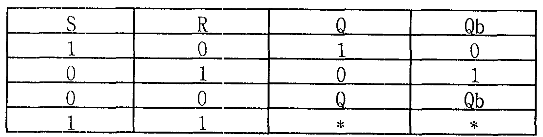
표 1과 같이 제 1 논리소자(11)로부터의 출력값이 하이 논리값을 갖고, 제 2 논리소자(12)로부터의 출력값이 로우 논리값을 가지면 출력버퍼(14)를 통해 제 1 클럭신호(CLK1)가 출력된다.As shown in Table 1, when the output value from the
출력된 후, 다음 클럭신호 기간에는 제 1 및 제 2 논리소자(11, 12)의 논리값이 반전되어 출력버퍼(14)를 통해 출력되는 신호가 없도록 제어한다.After the output, the logic values of the first and
게이트 신호가 출력버퍼(14)를 통해 출력되면, 제 2 클럭신호와 제 3 클럭신호에 의해 Qb 노드의 논리값이 교번되도록 제어된다.When the gate signal is output through the
이와 같이 3 상 클럭을 이용하는 경우에도, 전단의 출력신호 또는 스타트펄스와 후단의 출력신호 및 현재 단의 Q노드 논리값을 이용함으로서 본 발명의 기술상을 적용하는 것이 가능하다.Even in the case of using the three-phase clock in this manner, it is possible to apply the technical aspects of the present invention by using the output signal of the preceding stage or the start pulse and the output signal of the latter stage and the Q node logic value of the current stage.
5상 이상의 클럭을 이용하는 경우는, 앞서 설명한 실시예들에 비해 온오프가 반복되는 주기가 달라질 뿐, 위의 실시예들에 의해 용이하게 예측이 가능하다. 앞서 설명한 실시예에서도 3상 클럭중 3상을 선택적으로 이용하는 것이므로, 4상 중 1상을 제거하나 첨부하여도 본 발명의 기술적 사상을 벗어나지 않음을 밝혀둔다.In the case of using a clock of five or more phases, the period in which the on-off is repeated differs from the above-described embodiments, and the above-described embodiments can be easily predicted. In the above-described embodiment, since three phases of the three-phase clock are selectively used, one phase of the four phases is removed, but it is apparent that the accompanying drawings do not depart from the spirit of the present invention.
상술한 바와 같이, 본 발명에 따른 쉬프트 레지스터는 제 2 출력단에 하이논 리값과 로우 논리값이 반복되도록 공급전압을 제공한다. 이로인해, 본 발명에 따른 쉬프트 레지스터는 제 2 출력단에 누적되는 전압을 주기적으로 감소시켜 제 2 출력단의 누적 전압 스트레스를 정상적인 동작범위에서 유지하는 것이 가능하다. 따라서, 본 발명의 쉬프트 레지스터는 제 2 출력단의 누전전압 스트레스에 의한 열화로 인한 쉬프트 레지스터의 오동작을 방지하며, 열화로 인한 회로 및 소자의 파손을 방지하는 것이 가능하다.As described above, the shift register according to the present invention provides a supply voltage to the second output terminal such that the high logic value and the low logic value are repeated. As a result, the shift register according to the present invention can periodically reduce the voltage accumulated at the second output terminal to maintain the accumulated voltage stress of the second output terminal in the normal operating range. Accordingly, the shift register of the present invention prevents the shift register from malfunctioning due to deterioration due to the leakage voltage stress at the second output terminal, and prevents damage to circuits and elements due to degradation.
이상 설명한 내용을 통해 당업자라면 본 발명의 기술사상을 일탈하지 아니하는 행위에서 다양한 변경 및 수정이 가능함을 알 수 있을 것이다. 따라서, 본 발명의 기술적 범위는 명세서의 상세한 설명에 기재된 내용으로 한정되는 것이 아니라 특허 청구의 범위에 의해 정하여 져야만 할 것이다.Those skilled in the art will appreciate that various changes and modifications can be made in the acts that do not depart from the spirit of the present invention. Therefore, the technical scope of the present invention should not be limited to the contents described in the detailed description of the specification, but should be defined by the claims.
Claims (11)
Priority Applications (6)
| Application Number | Priority Date | Filing Date | Title |
|---|---|---|---|
| KR1020040118605A KR101137880B1 (en) | 2004-12-31 | 2004-12-31 | Shift Register And Method For Driving The Same |
| US11/167,620 US7333586B2 (en) | 2004-12-31 | 2005-06-27 | Shift register |
| CNB2005100798366A CN100508072C (en) | 2004-12-31 | 2005-06-29 | Shift register and method for driving the same |
| TW094122156A TWI294614B (en) | 2004-12-31 | 2005-06-30 | Shift register and method for driving the same |
| JP2005192306A JP4843267B2 (en) | 2004-12-31 | 2005-06-30 | Shift register |
| US11/963,634 US7529334B2 (en) | 2004-12-31 | 2007-12-21 | Shift register and method for driving the same |
Applications Claiming Priority (1)
| Application Number | Priority Date | Filing Date | Title |
|---|---|---|---|
| KR1020040118605A KR101137880B1 (en) | 2004-12-31 | 2004-12-31 | Shift Register And Method For Driving The Same |
Publications (2)
| Publication Number | Publication Date |
|---|---|
| KR20060079037A KR20060079037A (en) | 2006-07-05 |
| KR101137880B1 true KR101137880B1 (en) | 2012-04-20 |
Family
ID=36640429
Family Applications (1)
| Application Number | Title | Priority Date | Filing Date |
|---|---|---|---|
| KR1020040118605A KR101137880B1 (en) | 2004-12-31 | 2004-12-31 | Shift Register And Method For Driving The Same |
Country Status (5)
| Country | Link |
|---|---|
| US (2) | US7333586B2 (en) |
| JP (1) | JP4843267B2 (en) |
| KR (1) | KR101137880B1 (en) |
| CN (1) | CN100508072C (en) |
| TW (1) | TWI294614B (en) |
Families Citing this family (65)
| Publication number | Priority date | Publication date | Assignee | Title |
|---|---|---|---|---|
| JP4644087B2 (en) * | 2005-09-29 | 2011-03-02 | 株式会社 日立ディスプレイズ | Shift register circuit and display device using the same |
| KR101424794B1 (en) | 2006-01-07 | 2014-08-01 | 가부시키가이샤 한도오따이 에네루기 켄큐쇼 | Semiconductor device, and display device and electronic device having the same |
| JP4654923B2 (en) * | 2006-01-26 | 2011-03-23 | カシオ計算機株式会社 | Shift register circuit and display driving device |
| KR101154338B1 (en) * | 2006-02-15 | 2012-06-13 | 삼성전자주식회사 | Shift register, and scan drive circuit and display device having the same |
| US8330492B2 (en) | 2006-06-02 | 2012-12-11 | Semiconductor Energy Laboratory Co., Ltd. | Liquid crystal display device and electronic device |
| KR101255312B1 (en) * | 2006-06-29 | 2013-04-15 | 엘지디스플레이 주식회사 | Shift register and liquid crystal display device using the same |
| US8030303B2 (en) | 2006-07-11 | 2011-10-04 | Mitsubishi Tanabe Pharma Corporation | Salt of morpholine compound |
| KR101265333B1 (en) * | 2006-07-26 | 2013-05-20 | 엘지디스플레이 주식회사 | LCD and drive method thereof |
| KR101277152B1 (en) * | 2006-08-24 | 2013-06-21 | 삼성디스플레이 주식회사 | Gate driving circuit and display device having the same |
| TWI338275B (en) * | 2006-08-24 | 2011-03-01 | Au Optronics Corp | Shift register with lower coupling effect and the related lcd |
| EP1895545B1 (en) | 2006-08-31 | 2014-04-23 | Semiconductor Energy Laboratory Co., Ltd. | Liquid crystal display device |
| TWI347577B (en) * | 2006-09-01 | 2011-08-21 | Au Optronics Corp | Shift register with low stress |
| KR100796137B1 (en) | 2006-09-12 | 2008-01-21 | 삼성에스디아이 주식회사 | Shift register and organic light emitting display device using the same |
| JP5468196B2 (en) * | 2006-09-29 | 2014-04-09 | 株式会社半導体エネルギー研究所 | Semiconductor device, display device, and liquid crystal display device |
| TWI850180B (en) | 2006-09-29 | 2024-07-21 | 日商半導體能源研究所股份有限公司 | Semiconductor device |
| JP4932415B2 (en) | 2006-09-29 | 2012-05-16 | 株式会社半導体エネルギー研究所 | Semiconductor device |
| JP5116277B2 (en) | 2006-09-29 | 2013-01-09 | 株式会社半導体エネルギー研究所 | Semiconductor device, display device, liquid crystal display device, display module, and electronic apparatus |
| JP5525685B2 (en) * | 2006-10-17 | 2014-06-18 | 株式会社半導体エネルギー研究所 | Semiconductor device and electronic equipment |
| TWI427602B (en) * | 2006-10-17 | 2014-02-21 | Semiconductor Energy Lab | Pulse output circuit, shift register, and display device |
| TWI334144B (en) * | 2008-01-09 | 2010-12-01 | Au Optronics Corp | Shift register |
| TWI380274B (en) * | 2008-02-21 | 2012-12-21 | Chunghwa Picture Tubes Ltd | Shift register and liquid crystal display (lcd) |
| CN101562048B (en) * | 2008-04-15 | 2011-09-07 | 北京京东方光电科技有限公司 | Shift register and liquid crystal display grate drive device |
| TWI397883B (en) * | 2008-09-19 | 2013-06-01 | Hannstar Display Corp | Integrated gate driver circuit and driving method thereof |
| KR20160072845A (en) | 2008-10-24 | 2016-06-23 | 가부시키가이샤 한도오따이 에네루기 켄큐쇼 | Semiconductor device and method for manufacturing the same |
| WO2010061657A1 (en) | 2008-11-28 | 2010-06-03 | シャープ株式会社 | Scanning signal line driving circuit, shift register, and display device |
| CN102224539B (en) * | 2008-12-10 | 2013-10-23 | 夏普株式会社 | Scanning signal line driving circuit, shift register, and method of driving shift register |
| TWI394134B (en) * | 2008-12-12 | 2013-04-21 | Au Optronics Corp | Shift register with pre-pull-down circuit |
| TWI397050B (en) * | 2008-12-23 | 2013-05-21 | Au Optronics Corp | Liquid crystal display and shift register apparatus thereof |
| KR101579082B1 (en) * | 2008-12-23 | 2015-12-22 | 삼성디스플레이 주식회사 | Gate driving circuit and method of driving the same |
| US9741309B2 (en) * | 2009-01-22 | 2017-08-22 | Semiconductor Energy Laboratory Co., Ltd. | Method for driving display device including first to fourth switches |
| US8068577B2 (en) * | 2009-09-23 | 2011-11-29 | Au Optronics Corporation | Pull-down control circuit and shift register of using same |
| KR101721285B1 (en) * | 2009-10-09 | 2017-03-29 | 가부시키가이샤 한도오따이 에네루기 켄큐쇼 | Shift register and display device |
| TWI424401B (en) * | 2009-11-02 | 2014-01-21 | Chunghwa Picture Tubes Ltd | Display and gate driver circuit thereof |
| CN101783124B (en) * | 2010-02-08 | 2013-05-08 | 北京大学深圳研究生院 | Grid electrode driving circuit unit, a grid electrode driving circuit and a display device |
| KR101389120B1 (en) * | 2010-03-02 | 2014-04-25 | 가부시키가이샤 한도오따이 에네루기 켄큐쇼 | Pulse signal output circuit and shift register |
| JP5839896B2 (en) * | 2010-09-09 | 2016-01-06 | 株式会社半導体エネルギー研究所 | Display device |
| KR101296910B1 (en) * | 2010-10-20 | 2013-08-14 | 엘지디스플레이 주식회사 | Gate driver and organic light emitting diode display including the same |
| KR101747758B1 (en) * | 2010-12-06 | 2017-06-16 | 삼성디스플레이 주식회사 | Method of driving display panel and display apparatus for performing the same |
| KR20120091880A (en) * | 2011-02-10 | 2012-08-20 | 삼성디스플레이 주식회사 | Inverter and organic light emitting display device using the same |
| KR101340197B1 (en) * | 2011-09-23 | 2013-12-10 | 하이디스 테크놀로지 주식회사 | Shift register and Gate Driving Circuit Using the Same |
| TWI476743B (en) * | 2012-01-20 | 2015-03-11 | Innocom Tech Shenzhen Co Ltd | Shift register |
| US9036766B2 (en) * | 2012-02-29 | 2015-05-19 | Semiconductor Energy Laboratory Co., Ltd. | Semiconductor device |
| WO2013137069A1 (en) * | 2012-03-12 | 2013-09-19 | シャープ株式会社 | Shift register, driver circuit and display device |
| CN102651239B (en) * | 2012-03-29 | 2014-06-18 | 京东方科技集团股份有限公司 | Shift register, driver circuit and display device |
| US9171842B2 (en) | 2012-07-30 | 2015-10-27 | Semiconductor Energy Laboratory Co., Ltd. | Sequential circuit and semiconductor device |
| KR101463031B1 (en) * | 2012-09-27 | 2014-11-18 | 엘지디스플레이 주식회사 | Shift register |
| JP2014093100A (en) * | 2012-10-31 | 2014-05-19 | Kyocera Corp | Shift register circuit and image display device |
| KR101992158B1 (en) * | 2013-04-30 | 2019-09-30 | 엘지디스플레이 주식회사 | Gate shift register and display device using the same |
| US9424950B2 (en) * | 2013-07-10 | 2016-08-23 | Semiconductor Energy Laboratory Co., Ltd. | Semiconductor device |
| JP5809722B2 (en) * | 2014-03-03 | 2015-11-11 | 株式会社半導体エネルギー研究所 | Liquid crystal display |
| TWI484495B (en) | 2014-04-07 | 2015-05-11 | Au Optronics Corp | Shift register circuit |
| TWI537912B (en) * | 2014-07-21 | 2016-06-11 | 友達光電股份有限公司 | Shift register and flat panel display using the same |
| JP6521794B2 (en) | 2014-09-03 | 2019-05-29 | 株式会社半導体エネルギー研究所 | Semiconductor device and electronic device |
| CN104332181B (en) * | 2014-11-03 | 2018-11-13 | 合肥鑫晟光电科技有限公司 | A kind of shift register and gate drive apparatus |
| US9325311B1 (en) * | 2014-11-20 | 2016-04-26 | Innolux Corporation | Gate driver and display device using the same |
| JP6389341B2 (en) * | 2015-10-19 | 2018-09-12 | シャープ株式会社 | Shift register and display device including the same |
| CN106652867B (en) * | 2015-11-04 | 2020-02-21 | 上海和辉光电有限公司 | Shifting register unit, grid driving circuit and display panel |
| CN105321491B (en) * | 2015-11-18 | 2017-11-17 | 武汉华星光电技术有限公司 | Gate driving circuit and the liquid crystal display using gate driving circuit |
| CN105304011B (en) * | 2015-12-09 | 2019-11-19 | 京东方科技集团股份有限公司 | Shift register cell and its driving method, gate driving circuit and display device |
| JP6298491B2 (en) * | 2016-05-31 | 2018-03-20 | 株式会社半導体エネルギー研究所 | Display device |
| CN106205461B (en) * | 2016-09-30 | 2019-04-02 | 京东方科技集团股份有限公司 | Shift register cell, driving method, gate driving circuit and display device |
| KR102707009B1 (en) * | 2016-12-19 | 2024-09-12 | 엘지디스플레이 주식회사 | Gate driving circuit |
| CN107591139B (en) * | 2017-09-22 | 2020-12-25 | 京东方科技集团股份有限公司 | Scanning trigger unit, grid drive circuit, driving method of grid drive circuit and display device |
| KR20210085236A (en) | 2019-12-30 | 2021-07-08 | 엘지디스플레이 주식회사 | Gate driving circuit, and image display device including the same |
| KR20230154906A (en) * | 2021-03-05 | 2023-11-09 | 가부시키가이샤 한도오따이 에네루기 켄큐쇼 | Semiconductor devices, display devices, and electronic devices |
Citations (3)
| Publication number | Priority date | Publication date | Assignee | Title |
|---|---|---|---|---|
| JPH08263027A (en) * | 1995-03-06 | 1996-10-11 | Thomson Multimedia Sa | Shift register |
| KR20000055633A (en) * | 1999-02-09 | 2000-09-15 | 구본준 | Shift register circuit |
| KR20020069661A (en) * | 2001-02-27 | 2002-09-05 | 엘지.필립스 엘시디 주식회사 | Circuit for bi-directional driving liquid crystal display panel |
Family Cites Families (9)
| Publication number | Priority date | Publication date | Assignee | Title |
|---|---|---|---|---|
| JP4460822B2 (en) * | 2002-11-29 | 2010-05-12 | 東芝モバイルディスプレイ株式会社 | Bidirectional shift register, drive circuit using the same, and flat display device |
| KR100487439B1 (en) * | 2002-12-31 | 2005-05-03 | 엘지.필립스 엘시디 주식회사 | Circuit and method for bi-directional driving plat display device |
| KR20040097503A (en) * | 2003-05-12 | 2004-11-18 | 엘지.필립스 엘시디 주식회사 | Shift register |
| KR100583318B1 (en) * | 2003-12-17 | 2006-05-25 | 엘지.필립스 엘시디 주식회사 | Appartus and Method of Driving Liquid Crystal Display |
| KR101012972B1 (en) * | 2003-12-30 | 2011-02-10 | 엘지디스플레이 주식회사 | Active matrix display device |
| JP4645047B2 (en) * | 2004-03-05 | 2011-03-09 | カシオ計算機株式会社 | Shift register circuit, drive control method thereof, and drive control apparatus |
| US7289594B2 (en) * | 2004-03-31 | 2007-10-30 | Lg.Philips Lcd Co., Ltd. | Shift registrer and driving method thereof |
| US7828336B2 (en) * | 2004-12-09 | 2010-11-09 | Adroit Development, Inc. | Quick disconnect safety connector |
| KR101110133B1 (en) * | 2004-12-28 | 2012-02-20 | 엘지디스플레이 주식회사 | Shift register for LCD |
-
2004
- 2004-12-31 KR KR1020040118605A patent/KR101137880B1/en active IP Right Grant
-
2005
- 2005-06-27 US US11/167,620 patent/US7333586B2/en active Active
- 2005-06-29 CN CNB2005100798366A patent/CN100508072C/en active Active
- 2005-06-30 JP JP2005192306A patent/JP4843267B2/en active Active
- 2005-06-30 TW TW094122156A patent/TWI294614B/en active
-
2007
- 2007-12-21 US US11/963,634 patent/US7529334B2/en active Active
Patent Citations (3)
| Publication number | Priority date | Publication date | Assignee | Title |
|---|---|---|---|---|
| JPH08263027A (en) * | 1995-03-06 | 1996-10-11 | Thomson Multimedia Sa | Shift register |
| KR20000055633A (en) * | 1999-02-09 | 2000-09-15 | 구본준 | Shift register circuit |
| KR20020069661A (en) * | 2001-02-27 | 2002-09-05 | 엘지.필립스 엘시디 주식회사 | Circuit for bi-directional driving liquid crystal display panel |
Also Published As
| Publication number | Publication date |
|---|---|
| US7333586B2 (en) | 2008-02-19 |
| US7529334B2 (en) | 2009-05-05 |
| CN1797609A (en) | 2006-07-05 |
| US20080095297A1 (en) | 2008-04-24 |
| JP2006190437A (en) | 2006-07-20 |
| TW200623006A (en) | 2006-07-01 |
| US20060146978A1 (en) | 2006-07-06 |
| JP4843267B2 (en) | 2011-12-21 |
| KR20060079037A (en) | 2006-07-05 |
| CN100508072C (en) | 2009-07-01 |
| TWI294614B (en) | 2008-03-11 |
Similar Documents
| Publication | Publication Date | Title |
|---|---|---|
| KR101137880B1 (en) | Shift Register And Method For Driving The Same | |
| KR101057891B1 (en) | Shift register | |
| KR100698239B1 (en) | Shift Register Circuit | |
| KR101192777B1 (en) | A shift register | |
| US7336254B2 (en) | Shift register that suppresses operation failure due to transistor threshold variations, and liquid crystal driving circuit including the shift register | |
| US6891916B2 (en) | Shift register with built-in level shifter | |
| KR20230106558A (en) | Gate driving circuit and display device using the same | |
| CN109389927B (en) | Shift register, driving method thereof and grid driving circuit | |
| CN111477181B (en) | Gate driving circuit, display substrate, display device and gate driving method | |
| KR100566814B1 (en) | Shift register | |
| US11263988B2 (en) | Gate driving circuit and display device using the same | |
| US20060132182A1 (en) | Driver circuit, shift register, and liquid crystal driver circuit | |
| KR101768541B1 (en) | Shift Register | |
| JP4969322B2 (en) | Voltage generating circuit and image display device including the same | |
| KR20130110306A (en) | Shift register | |
| KR101027827B1 (en) | Shift register and method for driving the same | |
| CN108735142B (en) | Shift register, driving method thereof and grid driving circuit | |
| CN112908235B (en) | Gate drive unit, gate drive circuit and display device | |
| EP4145433A1 (en) | Shift register, gate electrode driving circuit, and gate electrode driving method | |
| KR20190069182A (en) | Shift resister and display device having the same | |
| CN110800039B (en) | GOA unit circuit, driving method, GOA circuit and display device | |
| KR101073263B1 (en) | Shift register and method for driving the same | |
| KR100583141B1 (en) | Level shifter and flat panel display having the same | |
| KR20110032838A (en) | Shift register | |
| KR20080049298A (en) | A shift register |
Legal Events
| Date | Code | Title | Description |
|---|---|---|---|
| A201 | Request for examination | ||
| E902 | Notification of reason for refusal | ||
| E701 | Decision to grant or registration of patent right | ||
| GRNT | Written decision to grant | ||
| FPAY | Annual fee payment |
Payment date: 20160329 Year of fee payment: 5 |
|
| FPAY | Annual fee payment |
Payment date: 20170320 Year of fee payment: 6 |
|
| FPAY | Annual fee payment |
Payment date: 20190318 Year of fee payment: 8 |