EP2270870B1 - Wide bandgap hemts with source connected field plates - Google Patents
Wide bandgap hemts with source connected field plates Download PDFInfo
- Publication number
- EP2270870B1 EP2270870B1 EP10183441.4A EP10183441A EP2270870B1 EP 2270870 B1 EP2270870 B1 EP 2270870B1 EP 10183441 A EP10183441 A EP 10183441A EP 2270870 B1 EP2270870 B1 EP 2270870B1
- Authority
- EP
- European Patent Office
- Prior art keywords
- field plate
- hemt
- gate
- layer
- semiconductor layers
- Prior art date
- Legal status (The legal status is an assumption and is not a legal conclusion. Google has not performed a legal analysis and makes no representation as to the accuracy of the status listed.)
- Expired - Lifetime
Links
Images

Classifications
-
- H—ELECTRICITY
- H10—SEMICONDUCTOR DEVICES; ELECTRIC SOLID-STATE DEVICES NOT OTHERWISE PROVIDED FOR
- H10D—INORGANIC ELECTRIC SEMICONDUCTOR DEVICES
- H10D30/00—Field-effect transistors [FET]
- H10D30/40—FETs having zero-dimensional [0D], one-dimensional [1D] or two-dimensional [2D] charge carrier gas channels
- H10D30/47—FETs having zero-dimensional [0D], one-dimensional [1D] or two-dimensional [2D] charge carrier gas channels having 2D charge carrier gas channels, e.g. nanoribbon FETs or high electron mobility transistors [HEMT]
- H10D30/471—High electron mobility transistors [HEMT] or high hole mobility transistors [HHMT]
- H10D30/475—High electron mobility transistors [HEMT] or high hole mobility transistors [HHMT] having wider bandgap layer formed on top of lower bandgap active layer, e.g. undoped barrier HEMTs such as i-AlGaN/GaN HEMTs
- H10D30/4755—High electron mobility transistors [HEMT] or high hole mobility transistors [HHMT] having wider bandgap layer formed on top of lower bandgap active layer, e.g. undoped barrier HEMTs such as i-AlGaN/GaN HEMTs having wide bandgap charge-carrier supplying layers, e.g. modulation doped HEMTs such as n-AlGaAs/GaAs HEMTs
-
- H—ELECTRICITY
- H10—SEMICONDUCTOR DEVICES; ELECTRIC SOLID-STATE DEVICES NOT OTHERWISE PROVIDED FOR
- H10D—INORGANIC ELECTRIC SEMICONDUCTOR DEVICES
- H10D30/00—Field-effect transistors [FET]
- H10D30/01—Manufacture or treatment
- H10D30/015—Manufacture or treatment of FETs having heterojunction interface channels or heterojunction gate electrodes, e.g. HEMT
-
- H—ELECTRICITY
- H10—SEMICONDUCTOR DEVICES; ELECTRIC SOLID-STATE DEVICES NOT OTHERWISE PROVIDED FOR
- H10D—INORGANIC ELECTRIC SEMICONDUCTOR DEVICES
- H10D62/00—Semiconductor bodies, or regions thereof, of devices having potential barriers
- H10D62/80—Semiconductor bodies, or regions thereof, of devices having potential barriers characterised by the materials
- H10D62/85—Semiconductor bodies, or regions thereof, of devices having potential barriers characterised by the materials being Group III-V materials, e.g. GaAs
- H10D62/8503—Nitride Group III-V materials, e.g. AlN or GaN
-
- H—ELECTRICITY
- H10—SEMICONDUCTOR DEVICES; ELECTRIC SOLID-STATE DEVICES NOT OTHERWISE PROVIDED FOR
- H10D—INORGANIC ELECTRIC SEMICONDUCTOR DEVICES
- H10D64/00—Electrodes of devices having potential barriers
- H10D64/111—Field plates
-
- H—ELECTRICITY
- H10—SEMICONDUCTOR DEVICES; ELECTRIC SOLID-STATE DEVICES NOT OTHERWISE PROVIDED FOR
- H10D—INORGANIC ELECTRIC SEMICONDUCTOR DEVICES
- H10D64/00—Electrodes of devices having potential barriers
- H10D64/20—Electrodes characterised by their shapes, relative sizes or dispositions
- H10D64/23—Electrodes carrying the current to be rectified, amplified, oscillated or switched, e.g. sources, drains, anodes or cathodes
- H10D64/251—Source or drain electrodes for field-effect devices
-
- H—ELECTRICITY
- H10—SEMICONDUCTOR DEVICES; ELECTRIC SOLID-STATE DEVICES NOT OTHERWISE PROVIDED FOR
- H10D—INORGANIC ELECTRIC SEMICONDUCTOR DEVICES
- H10D64/00—Electrodes of devices having potential barriers
- H10D64/20—Electrodes characterised by their shapes, relative sizes or dispositions
- H10D64/27—Electrodes not carrying the current to be rectified, amplified, oscillated or switched, e.g. gates
- H10D64/311—Gate electrodes for field-effect devices
- H10D64/411—Gate electrodes for field-effect devices for FETs
Definitions
- the present invention relates to high-electron mobility transistors and particularly to such transistors utilizing field plates.
- AlGaN/GaN semiconductor materials have helped advance the development of AlGaN/GaN transistors, such as high electron mobility transistors (HEMTs) for high frequency, high temperature and high power applications.
- HEMTs high electron mobility transistors
- AlGaN/GaN has large bandgaps, high peak and saturation electron velocity values [ B. Gelmont, K. Kim and M. Shur, Monte Carlo Simulation of Electron Transport in Gallium Nitride, J.Appl.Phys. 74, (1993), pp. 1818-1821 ].
- AlGaN/GaN HEMTs can also have 2DEG sheet densities in excess of 10 13 cm -2 and relatively high electron mobility (up to 2019 cm 2 /Vs) [ R.
- AlGaN/GaN HEMTs have been grown on sapphire substrates and have shown a power density of 4.6 W/mm and a total power of 7.6 W [ Y.F. Wu et al., GaN-Based FETs for Microwave Power Amplification, IEICE Trans. Electron. E-82-C, (1999). pp. 1895-1905 ]. More recently, AlGaN/GaN HEMTs grown on SiC have shown a power density of 9.8 W/mm at 8 GHz [ Y.F. Wu, et al., Very-High Power Density AlGaN/GaN HEMTs, IEEE Trans.Electron.Dev. 48, (2001), pp.
- U.S. Patent number 5,192,987 to Khan et al. discloses GaN/AlGaN based HEMTs grown on a buffer and a substrate.
- Other AlGaN/GaN HEMTs and field effect transistors (FETs) have been described by Gaska et al., High-Temperature Performance of AlGaN/GaN HFET's on SiC Substrates, IEEE Electron Device Letters, 18, (1997), pp. 492-494 ; and Ping et al., DC and Microwave Performance of High Current AlGaN Heterostructure Field Effect Transistors Grown on P-type SiC Substrates, IEEE Electron Devices Letters 19, (1998), pp. 54-56 .
- SiN passivation has been successfully employed to alleviate this trapping problem resulting in high performance devices with power densities over 10W/mm at 10 Ghz.
- SiN Silicon nitride
- U.S. Patent No. 6,586,781 discloses methods and structures for reducing the trapping effect in GaN-based transistors. However, due to the high electric fields existing in these structures, charge trapping is still an issue.
- Published U.S. patent application no. 2002/1373118 discloses a field effect transistor structure that is formed with a body semiconductor layer having source , body, drift region and drain.
- An upper semiconductor layer is separated from the body by an oxide layer.
- the upper semiconductor layer is doped to have a gate region arranged over the body, a field plate region arranged over the drift region and at least one p-n junction forming at least one diode between the field plate region and the gate region.
- a source contact is connected to both the source and the field plate region. The connection between the source and the field plate does not run over the active area and at a vertical level higher than that of the field plate.
- Published U.S. patent application no. 2003/222327 relates to a semiconductor device which includes a first-first conductivity type semiconductor layer having a cell region portion and a junction terminating region portion.
- Published U.S. patent application no. 2002/005528 relates to a compound semiconductor device which includes a cap layer formed on a channel layer and an insulating film formed on the cap layer, and a ⁇ -shaped gate electrode is provided in a gate recess opening, wherein an extension part of the ⁇ -shaped gate electrode extends over the insulating film toward a drain electrode, and the total thickness of the insulating film and the cap layer being is set such that the electric field formed right underneath the extension part of the gate electrode includes a component acting in a direction perpendicular to the substrate.
- the present invention provides high electron-mobility transistors with a field plate connected to the source electrode, according to claim 1.
- Wide bandgap transistor structures generally include an active region, with metal source and drain electrodes formed in electrical contact with the active region, and a gate electrode formed between the source and drain electrodes for modulating electric fields within the active region.
- a spacer layer is formed above the active region.
- the spacer layer can comprise a dielectric layer, or a combination of multiple dielectric layers.
- a conductive field plate is formed above the spacer layer and extends a distance L f from the edge of the gate electrode toward the drain electrode.
- the field plate can be electrically connected to the source electrode.
- This field plate arrangement can reduce the peak electric field in the device, resulting in increased breakdown voltage and reduced trapping. The reduction of the electric field can also yield other benefits such as reduced leakage currents and enhanced reliability.
- the field plate electrically connected to the source electrode By having the field plate electrically connected to the source electrode, the reduced gain and instability resulting from gate connected field plates is reduced.
- the shielding effect of a source-connected field plate can reduce C gd , which enhances input-output isolation.
- a high electron mobility transistor typically includes a buffer layer and a barrier layer on the buffer layer.
- a two dimensional electron gas (2DEG) layer/channel is formed at the junction between the buffer layer and the barrier layer.
- a gate electrode is formed on the barrier layer between source and drain electrodes.
- a spacer layer is formed on the barrier layer covering the barrier layer between the gate and drain electrode such that a field plate is formed on the spacer layer in electric isolation from the barrier layer.
- the spacer layer also covers the gate such that the field plate can overlap the gate while remaining in electrical isolation from the gate and the barrier layer.
- the spacer layer covers the gate and the surface of the barrier layer between the gate and the source and drain electrodes.
- the spacer layer can comprise a dielectric layer, or a combination of multiple dielectric layers. Different dielectric materials can be used such as a SiN, SiO2, Si, Ge, MgOx, MgNx, ZnO, SiNx, SiOx, alloys or layer sequences thereof, or epitaxial materials as described below.
- a conductive field plate is formed on the spacer layer and extends a distance L f from the edge of the gate towards the drain electrode, with the field plate and gate electrode typically being formed during separate deposition steps.
- the field plate is also electrically connected to the source electrode.
- FIGs. 1 and 2 show one embodiment of a nitride based HEMT 10 according to the present invention which comprises a substrate 12 of silicon carbide, sapphire, spinet, ZnO, silicon, gallium nitride, aluminum nitride, or any other material capable of supporting growth of a Group-III nitride material.
- the substrate 12 can comprise semi-insulating 4H-SiC commercially available from Cree, Inc. of Durham, NC.
- a nucleation layer 14 can be formed on the substrate 12 to reduce the lattice mismatch between the substrate 12 and the next layer in the HEMT 10.
- the nucleation layer 14 should be approximately 1000 angstroms ( ⁇ ) thick, although other thicknesses can be used.
- the nucleation layer 14 can be formed on the substrate 12 using known semiconductor growth techniques such as Metal Oxide Chemical Vapor Deposition (MOCVD), Hydride Vapor Phase Epitaxy (HVPE), or Molecular Beam Epitaxy (MBE).
- MOCVD Metal Oxide Chemical Vapor Deposition
- HVPE Hydride Vapor Phase Epitaxy
- MBE Molecular Beam Epitaxy
- the formation of the nucleation layer 14 can depend on the material used for the substrate 12. For example, methods of forming a nucleation layer 14 on various substrates are taught in U.S. Patents 5,290,393 and 5,686,738 . Methods of forming nucleation layers on silicon carbide substrates are disclosed in U.S. Patents 5,393,993 , 5,523,589 , and 5,739,554 .
- the buffer layer 16 comprises a GaN layer that is approximately 2 ⁇ m thick, with part of the layer doped with Fe.
- a barrier layer 18 is formed on the buffer layer 16 such that the buffer layer 16 is sandwiched between the barrier layer 18 and the nucleation layer 14.
- Each of the buffer layer 16 and barrier layer 18 can comprise doped or undoped layers of Group III-nitride materials.
- the barrier layer 18 can comprise one or more layers of different materials such as InGaN, AlGaN, AlN, or combinations thereof.
- the barrier layer 18 comprises 0.8 nm of AlN and 22.5 nm of Al x Ga 1-x N (x ⁇ 0.195, as measured by photo luminescence). Exemplary structures are illustrated in U.S. Patent Nos. 6,316,793 , 6,586,781 , 6,548,333 and U.S. Published Patent Application Nos.
- nitride based HEMT structures are illustrated in U.S. Patents 5,192,987 and 5,296,395 .
- the buffer and barrier layers 16, 18 can be made using the same methods used to grow the nucleation layer 14.
- a two dimensional electron gas (2DEG) layer/channel 17 is formed at the heterointerface between the buffer and barrier layer 16, 18. Electric isolation between the devices is achieved with mesa etch or ion implementation outside the active area of the HEMT.
- Metal source and drain electrodes 20, 22 are formed making ohmic contact through the barrier layer 18, and a gate 24 is formed on the barrier layer 18 between the source and drain electrodes 20, 22. Electric current can flow between the source and drain electrodes 20, 22 through a two-dimensional electron gas (2DEG) 17 induced at the heterointerface between the buffer layer 16 and the barrier layer 18 when the gate electrode 24 is biased at the appropriate level.
- 2DEG two-dimensional electron gas
- the source and drain electrodes 20, 22 can be made of different materials including but not limited to alloys of titanium, aluminum, gold or nickel.
- the gate 24 can also be made of different materials including but not limited to nickel, gold, platinum, titanium, chromium, alloys of titanium and tungsten, or platinum silicide.
- the gate 24 can have many different lengths, with a preferred gate length (L g ) being approximately 0.5 microns. As best shown in FIG. 1 , the gate 24 is connected to and contacted at a gate electrode 28. As described below, in other transistor embodiments according to the present invention the gate 24 can be at least partially recessed in barrier layer 18.
- a non-conducting spacer layer 26 is formed over the gate 24 and the surface of the barrier layer 18 between the gate 24 and the source and drain electrodes 20, 22.
- the spacer layer 26 can comprise a layer of non-conducting material such as a dielectric. Alternatively, it can comprise a number of different layers of dielectrics or a combination of dielectric layers.
- the spacer layer can be many different thicknesses, with a suitable range of thicknesses being approximately 0.05 to 2 microns.
- the spacer layer 26 may be formed before device metallization, in which case the spacer layer 26 can comprise an epitaxial material such as a Group III nitride material having different Group III elements such as alloys of Al, Ga, or In, with a suitable spacer layer material being Al x Ga 1-x N (0 ⁇ x ⁇ 1).
- the spacer layer 26 can be grown using the same epitaxial growth method.
- the spacer layer 26 is then etched such that the gate 24, source electrode 20 and drain electrode 22 can be properly formed in contact with the buffer layer 18 and the 2DEG 17.
- a field plate can then be deposited on the spacer layer between the gate 24 and drain electrode 22. In those embodiments where the field plate overlaps the gate, an additional spacer layer of dielectric material should then be included at least partially over the gate to isolate the gate from the field plate.
- a field plate 30 is formed on the spacer layer 26 between the gate 24 and the drain electrode 22, with the field plate 30 being in close proximity to the gate 24 but not overlapping it.
- a space between the gate 24 and field plate (L gf ) remains and should be wide enough to isolate from the field plate 30, while being small enough to maximize the field effect provided by the field plate 30. If L gf is too wide the field effect can be reduced. In one embodiment according to the present invention L gf should be approximately 0.4 microns or less, although larger and smaller spaces can also be used.
- the field plate 30 can extend different distances L f from the edge of the gate 24, with a suitable range of distances for L f being approximately 0.1 to 2 microns.
- the field plate 30 can comprise many different conductive materials with a suitable material being a metal, or combinations of metals, deposited using standard metallization methods.
- the field plate 30 comprises titanium/gold or nickel/gold.
- FIG. 1 shows two connection structures that can be used according to the present invention, although other connection structures can also be used.
- Conductive buses 32 can be formed on the spacer layer 26 to extend between the field plate 30 and the source electrode 20, which does not fall under the scope of the claimed invention, however. Different numbers of buses 32 can be used although the greater the number of buses the greater the unwanted capacitance that can be introduced by the buses and the busses 32 should cover less than all of the all of the topmost surface between gate 24 and source electrode 20.
- the buses should have a sufficient number so that current effectively spreads from the source electrode 20 into the field plate 30, while not covering too much of the HEMT's active region, with a suitable number of buses 32 being two.
- the field plate 30 is electrically connected to the source electrode 20 through a conductive path 34 that does not run over the active regions of the HEMT 10, the field plate and the source electrode 20. As shown in FIG. 1 , the field plate 30 extends beyond the width of the active area and the path 34 runs outside the active area of the HEMT at the side opposite the gate electrode 28.
- the conductive path could run outside the active area of the HEMT 10 on the side of the gate electrode 28, or the HEMT 10 could include two or more conductive paths running out the same or different sides of the HEMT 10.
- the active structure can be covered by a dielectric passivation layer (not shown), such as silicon nitride.
- a dielectric passivation layer such as silicon nitride.
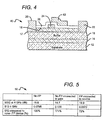
- FIGs. 3 and 4 show another embodiment of a HEMT 40 according to the present invention having many features that are similar to those in HEMT 10 of FIGs. 1 and 2 .
- the same reference numerals are used and the features are introduced without full description with the understanding that the description of the features above applies equally to the HEMT 40.
- the HEMT 40 comprises a substrate 12, nucleation layer 14, buffer layer 16, 2DEG 17, barrier layer 18, source electrode 20, drain electrode 22, gate 24, spacer layer 26 and gate electrode 28.
- the HEMT 40 also comprises a field plate 42 that is formed on the spacer layer 26 primarily between the gate 24 and the drain electrode 22, but also overlapping a portion of the gate 24.
- L gf is small, which can present some difficulties during fabrication.
- the field plate 42 overlap the gate 24 the HEMT 40 can be fabricated without having to meet the tolerances of L gf .
- the overlapping section of the field plate 42 can introduce additional unwanted capacitance. In determining whether to use a field plate 30 or 42 the ease of manufacturing using field plate 42 must be balanced with the reduced capacitance provided by field plate 30.
- the HEMT 40 also comprises either buses 44 or a conductive path 46 to electrically connect the field plate 42 to the source electrode 20, only the path 46 falling under the scope of the claimed invention.
- the active structure can also be covered by a dielectric passivation layer (not shown), such as silicon nitride.
- FIG. 5 shows a table 50 comparing the operating characteristics of GaN based HEMTs with no field plate to HEMTs having a field plate connected to the gate, and field plate connected to the source.
- HEMTs with source connected field plates exhibit improved maximum stable gain (MSG) and reduced reverse power transmission (S 12 ).
- MSG maximum stable gain
- S 12 of a HEMT with a gate connected field plate is increased by 71% at 4 GHz, while that of the device with a source connected field plate is actually reduced by 28%.
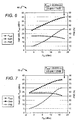
- FIG. 6 is a graph 60 showing the performance of a gate connected field plate device
- FIG. 7 is a graph 70 showing the performance of a source connected field plate device.
- Both field plate devices were able to operate at 118 V dc bias wherein tuning was optimized for the best combination of gain, PAE and output power at 3 dB compression (P 3dB ). While both devices generate power densities of approximately 20 W/mm, the source connected field plate device provides a 7 dB higher associated gain. With the achieved large-signal gain of 21 dB at 4 GHz and the estimated voltage swing of 224V, the voltage-frequency-gain product approaches 10 kV-GHz.
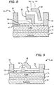
- FIG. 8 shows another embodiment of a HEMT 80 according to the present invention that has many features similar to those in HEMTs 10 and 40, including a substrate 12, nucleation layer 14, buffer layer 16, 2DEG 17, barrier layer 18, source electrode 20, and drain electrode 22.
- HEMT 80 has a gamma ( ⁇ ) shaped gate 82 that is particularly adapted to high frequency operation.
- the gate length (L g ) is one of the important device dimensions in determining the speed of the device, and with higher frequency devices the gate length is shorter. Shorter gate length can lead to high resistance that can negatively impact high frequency operation.
- T-gates are commonly used in high frequency operation, but it can be difficult to achieve a well-coupled placement of a field plate with a T-gate.
- the gamma gate 82 provides for low gate resistance and allows for controlled definition of the gate footprint.
- a spacer layer 84 is included that covers the gamma gate 82 and the surface of barrier layer 18 between the gamma gate 82 and the source and drain electrodes 20, 22. A space can remain between the horizontal portion of the gamma gate 82 and the top of the spacer layer 84.
- the HEMT 80 also includes a field plate 86 on the spacer layer 84 that overlaps that gamma gate 82, with the field plate 86 preferably deposited on the side of the gamma gate 82 not having a horizontal overhanging section. This arrangement allows for tight placement and effective coupling between the field plate 86 and the active layers below it.
- the field plate can be similarly arranged to field plate 86, but instead of overlapping the gate, there can be a space between the edge of the gate and the field plate similar to space Lgf shown in FIG. 2 .
- the field plate 86 can be electrically connected to the source electrode 20 in many different ways. Because of the space between the lower surface of the horizontal section of the gate 82 and the spacer layer 84, it can be difficult to provide a conductive path directly between the field plate 86 and the source electrode 20. Instead, according to the invention a conductive path can be included between the field plate 86 and the source electrode 20 that runs outside the active area of the HEMT 80. Alternatively and not falling under the scope of the present invention, the gamma gate 82 can be completely covered by the spacer layer 84 with the space under the gate's horizontal section filled. Conductive paths can then run directly from the field plate 86 to the source electrode over the spacer layer 84. The active structure can then be covered by a dielectric passivation layer (not shown).
- FIG. 9 shows still another HEMT 90 according to the present invention that can also be arranged with a source connected field plate.
- HEMT 90 also has many features similar to those in HEMTs 10 and 40 in FIGs. 1-4 , including a substrate 12, nucleation layer 14, buffer layer 16, 2DEG 17, barrier layer 18, source electrode 20, and drain electrode 22.
- the gate 92 is recessed in the barrier layer 18, and is covered by a spacer layer 94. In other embodiments the bottom surface of the gate can be only partially recessed or different portions of the gate can be recessed to different depths in the barrier layer 18.
- a field plate 96 is arranged on the spacer layer 94 and is electrically connected to the source electrode 20 and the active structure can be covered by a dielectric passivation layer (not shown).
- the embodiments above provide wide bandgap transistors, particularly HEMTs, with improved power at microwave and millimeter wave frequencies.
- the HEMTs exhibit simultaneous high gain, high power, and more stable operation due to higher input-output isolation.
- the structure could be extended to larger dimensions for high voltage applications at lower frequencies.
Landscapes
- Junction Field-Effect Transistors (AREA)
- Electrodes Of Semiconductors (AREA)
Applications Claiming Priority (4)
| Application Number | Priority Date | Filing Date | Title |
|---|---|---|---|
| US57051904P | 2004-05-11 | 2004-05-11 | |
| US10/958,970 US7550783B2 (en) | 2004-05-11 | 2004-10-04 | Wide bandgap HEMTs with source connected field plates |
| PCT/US2005/009884 WO2005114744A2 (en) | 2004-05-11 | 2005-03-24 | Wide bandgap hemts with source connected field plates |
| EP05731252.2A EP1751803B1 (en) | 2004-05-11 | 2005-03-24 | Wide bandgap hemts with source connected field plates |
Related Parent Applications (3)
| Application Number | Title | Priority Date | Filing Date |
|---|---|---|---|
| EP05731252.2 Division | 2005-03-24 | ||
| EP05731252.2A Division EP1751803B1 (en) | 2004-05-11 | 2005-03-24 | Wide bandgap hemts with source connected field plates |
| EP05731252.2A Division-Into EP1751803B1 (en) | 2004-05-11 | 2005-03-24 | Wide bandgap hemts with source connected field plates |
Publications (2)
| Publication Number | Publication Date |
|---|---|
| EP2270870A1 EP2270870A1 (en) | 2011-01-05 |
| EP2270870B1 true EP2270870B1 (en) | 2021-08-04 |
Family
ID=34964651
Family Applications (4)
| Application Number | Title | Priority Date | Filing Date |
|---|---|---|---|
| EP05731252.2A Expired - Lifetime EP1751803B1 (en) | 2004-05-11 | 2005-03-24 | Wide bandgap hemts with source connected field plates |
| EP10183607.0A Expired - Lifetime EP2270871B1 (en) | 2004-05-11 | 2005-03-24 | Wide bandgap hemts with source connected field plates |
| EP18192908.4A Pending EP3432362A1 (en) | 2004-05-11 | 2005-03-24 | Wide bandgap hemts with source connected field plates |
| EP10183441.4A Expired - Lifetime EP2270870B1 (en) | 2004-05-11 | 2005-03-24 | Wide bandgap hemts with source connected field plates |
Family Applications Before (3)
| Application Number | Title | Priority Date | Filing Date |
|---|---|---|---|
| EP05731252.2A Expired - Lifetime EP1751803B1 (en) | 2004-05-11 | 2005-03-24 | Wide bandgap hemts with source connected field plates |
| EP10183607.0A Expired - Lifetime EP2270871B1 (en) | 2004-05-11 | 2005-03-24 | Wide bandgap hemts with source connected field plates |
| EP18192908.4A Pending EP3432362A1 (en) | 2004-05-11 | 2005-03-24 | Wide bandgap hemts with source connected field plates |
Country Status (8)
| Country | Link |
|---|---|
| US (3) | US7550783B2 (OSRAM) |
| EP (4) | EP1751803B1 (OSRAM) |
| JP (3) | JP5390768B2 (OSRAM) |
| KR (1) | KR101101671B1 (OSRAM) |
| CN (1) | CN100580954C (OSRAM) |
| CA (1) | CA2566756C (OSRAM) |
| TW (2) | TWI397998B (OSRAM) |
| WO (1) | WO2005114744A2 (OSRAM) |
Families Citing this family (149)
| Publication number | Priority date | Publication date | Assignee | Title |
|---|---|---|---|---|
| JP2005527102A (ja) | 2001-07-24 | 2005-09-08 | クリー インコーポレイテッド | 高電子移動度トランジスタ及びその製造方法 |
| KR100514379B1 (ko) * | 2002-07-23 | 2005-09-13 | 김용철 | 사과를 이용한 주류제조방법 |
| US7501669B2 (en) | 2003-09-09 | 2009-03-10 | Cree, Inc. | Wide bandgap transistor devices with field plates |
| US7573078B2 (en) * | 2004-05-11 | 2009-08-11 | Cree, Inc. | Wide bandgap transistors with multiple field plates |
| US7550783B2 (en) * | 2004-05-11 | 2009-06-23 | Cree, Inc. | Wide bandgap HEMTs with source connected field plates |
| US9773877B2 (en) * | 2004-05-13 | 2017-09-26 | Cree, Inc. | Wide bandgap field effect transistors with source connected field plates |
| JP4744109B2 (ja) | 2004-07-20 | 2011-08-10 | トヨタ自動車株式会社 | 半導体装置とその製造方法 |
| US20060073621A1 (en) * | 2004-10-01 | 2006-04-06 | Palo Alto Research Center Incorporated | Group III-nitride based HEMT device with insulating GaN/AlGaN buffer layer |
| US11791385B2 (en) * | 2005-03-11 | 2023-10-17 | Wolfspeed, Inc. | Wide bandgap transistors with gate-source field plates |
| US20060226442A1 (en) | 2005-04-07 | 2006-10-12 | An-Ping Zhang | GaN-based high electron mobility transistor and method for making the same |
| US7855401B2 (en) | 2005-06-29 | 2010-12-21 | Cree, Inc. | Passivation of wide band-gap based semiconductor devices with hydrogen-free sputtered nitrides |
| US7525122B2 (en) * | 2005-06-29 | 2009-04-28 | Cree, Inc. | Passivation of wide band-gap based semiconductor devices with hydrogen-free sputtered nitrides |
| US7598576B2 (en) * | 2005-06-29 | 2009-10-06 | Cree, Inc. | Environmentally robust passivation structures for high-voltage silicon carbide semiconductor devices |
| WO2008027027A2 (en) * | 2005-09-07 | 2008-03-06 | Cree, Inc | Transistor with fluorine treatment |
| JP5162823B2 (ja) * | 2005-12-08 | 2013-03-13 | 三菱電機株式会社 | 半導体装置及び半導体装置の製造方法 |
| US7388236B2 (en) * | 2006-03-29 | 2008-06-17 | Cree, Inc. | High efficiency and/or high power density wide bandgap transistors |
| EP1921669B1 (en) | 2006-11-13 | 2015-09-02 | Cree, Inc. | GaN based HEMTs with buried field plates |
| US7692263B2 (en) | 2006-11-21 | 2010-04-06 | Cree, Inc. | High voltage GaN transistors |
| US8212290B2 (en) | 2007-03-23 | 2012-07-03 | Cree, Inc. | High temperature performance capable gallium nitride transistor |
| CN103441144B (zh) * | 2007-06-06 | 2016-09-14 | 苏州捷芯威半导体有限公司 | Hemt器件及其制造方法 |
| US20090072269A1 (en) * | 2007-09-17 | 2009-03-19 | Chang Soo Suh | Gallium nitride diodes and integrated components |
| CN101252088B (zh) * | 2008-03-28 | 2010-04-14 | 西安电子科技大学 | 一种增强型A1GaN/GaN HEMT器件的实现方法 |
| US8519438B2 (en) * | 2008-04-23 | 2013-08-27 | Transphorm Inc. | Enhancement mode III-N HEMTs |
| US8289065B2 (en) | 2008-09-23 | 2012-10-16 | Transphorm Inc. | Inductive load power switching circuits |
| CN101419985B (zh) * | 2008-12-01 | 2011-06-01 | 西安电子科技大学 | 绝缘栅型源场板异质结场效应晶体管 |
| US7898004B2 (en) | 2008-12-10 | 2011-03-01 | Transphorm Inc. | Semiconductor heterostructure diodes |
| US7884394B2 (en) * | 2009-02-09 | 2011-02-08 | Transphorm Inc. | III-nitride devices and circuits |
| SE533700C2 (sv) * | 2009-03-24 | 2010-12-07 | Transic Ab | Bipolär transistor i kiselkarbid |
| US8754496B2 (en) * | 2009-04-14 | 2014-06-17 | Triquint Semiconductor, Inc. | Field effect transistor having a plurality of field plates |
| US8008977B2 (en) * | 2009-04-14 | 2011-08-30 | Triquint Semiconductor, Inc. | Field-plated transistor including feedback resistor |
| US8742459B2 (en) | 2009-05-14 | 2014-06-03 | Transphorm Inc. | High voltage III-nitride semiconductor devices |
| US8168486B2 (en) * | 2009-06-24 | 2012-05-01 | Intersil Americas Inc. | Methods for manufacturing enhancement-mode HEMTs with self-aligned field plate |
| WO2010151856A2 (en) | 2009-06-26 | 2010-12-29 | Cornell University | Chemical vapor deposition process for aluminum silicon nitride |
| WO2010151855A2 (en) | 2009-06-26 | 2010-12-29 | Cornell University | Iii-v semiconductor structures including aluminum-silicon nitride passivation |
| US8390000B2 (en) | 2009-08-28 | 2013-03-05 | Transphorm Inc. | Semiconductor devices with field plates |
| CN102013437B (zh) * | 2009-09-07 | 2014-11-05 | 苏州捷芯威半导体有限公司 | 半导体器件及其制造方法 |
| US7999287B2 (en) | 2009-10-26 | 2011-08-16 | Infineon Technologies Austria Ag | Lateral HEMT and method for the production of a lateral HEMT |
| US8389977B2 (en) | 2009-12-10 | 2013-03-05 | Transphorm Inc. | Reverse side engineered III-nitride devices |
| WO2011100304A1 (en) | 2010-02-09 | 2011-08-18 | Massachusetts Institute Of Technology | Dual-gate normally-off nitride transistors |
| EP2383786B1 (en) | 2010-04-29 | 2018-08-15 | Ampleon Netherlands B.V. | Semiconductor transistor comprising two electrically conductive shield elements |
| US8829999B2 (en) | 2010-05-20 | 2014-09-09 | Cree, Inc. | Low noise amplifiers including group III nitride based high electron mobility transistors |
| JP5688556B2 (ja) | 2010-05-25 | 2015-03-25 | パナソニックIpマネジメント株式会社 | 電界効果トランジスタ |
| JP2011249728A (ja) * | 2010-05-31 | 2011-12-08 | Toshiba Corp | 半導体装置および半導体装置の製造方法 |
| JP5712516B2 (ja) * | 2010-07-14 | 2015-05-07 | 住友電気工業株式会社 | 半導体装置 |
| JP5649347B2 (ja) | 2010-07-20 | 2015-01-07 | 住友電工デバイス・イノベーション株式会社 | 半導体装置 |
| US8513703B2 (en) | 2010-10-20 | 2013-08-20 | National Semiconductor Corporation | Group III-nitride HEMT with multi-layered substrate having a second layer of one conductivity type touching a top surface of a first layers of different conductivity type and a method for forming the same |
| JP2012109492A (ja) * | 2010-11-19 | 2012-06-07 | Sanken Electric Co Ltd | 化合物半導体装置 |
| US8742460B2 (en) | 2010-12-15 | 2014-06-03 | Transphorm Inc. | Transistors with isolation regions |
| US8643062B2 (en) | 2011-02-02 | 2014-02-04 | Transphorm Inc. | III-N device structures and methods |
| JP5866773B2 (ja) * | 2011-02-25 | 2016-02-17 | 富士通株式会社 | 化合物半導体装置及びその製造方法 |
| US8716141B2 (en) | 2011-03-04 | 2014-05-06 | Transphorm Inc. | Electrode configurations for semiconductor devices |
| US8772842B2 (en) | 2011-03-04 | 2014-07-08 | Transphorm, Inc. | Semiconductor diodes with low reverse bias currents |
| JP5597581B2 (ja) * | 2011-03-23 | 2014-10-01 | 株式会社東芝 | 窒化物半導体装置及びその製造方法 |
| SE1150386A1 (sv) | 2011-05-03 | 2012-11-04 | Fairchild Semiconductor | Bipolär transistor av kiselkarbid med förbättrad genombrottsspänning |
| US8901604B2 (en) | 2011-09-06 | 2014-12-02 | Transphorm Inc. | Semiconductor devices with guard rings |
| JP5979836B2 (ja) * | 2011-09-09 | 2016-08-31 | ルネサスエレクトロニクス株式会社 | 半導体装置および半導体装置の製造方法 |
| US9257547B2 (en) | 2011-09-13 | 2016-02-09 | Transphorm Inc. | III-N device structures having a non-insulating substrate |
| KR101616157B1 (ko) * | 2011-09-21 | 2016-04-27 | 한국전자통신연구원 | 전력 반도체 소자 및 그 제조 방법 |
| US8772833B2 (en) * | 2011-09-21 | 2014-07-08 | Electronics And Telecommunications Research Institute | Power semiconductor device and fabrication method thereof |
| US8598937B2 (en) | 2011-10-07 | 2013-12-03 | Transphorm Inc. | High power semiconductor electronic components with increased reliability |
| US8664718B2 (en) * | 2011-11-30 | 2014-03-04 | Taiwan Semiconductor Manufacturing Company, Ltd. | Power MOSFETs and methods for forming the same |
| US10002957B2 (en) | 2011-12-21 | 2018-06-19 | Power Integrations, Inc. | Shield wrap for a heterostructure field effect transistor |
| US9165766B2 (en) | 2012-02-03 | 2015-10-20 | Transphorm Inc. | Buffer layer structures suited for III-nitride devices with foreign substrates |
| JP2013182992A (ja) * | 2012-03-01 | 2013-09-12 | Toshiba Corp | 半導体装置 |
| JP2013183061A (ja) * | 2012-03-02 | 2013-09-12 | Toshiba Corp | 半導体装置 |
| JP2013183062A (ja) * | 2012-03-02 | 2013-09-12 | Toshiba Corp | 半導体装置 |
| JP2013183060A (ja) | 2012-03-02 | 2013-09-12 | Toshiba Corp | 半導体装置 |
| JP5895666B2 (ja) * | 2012-03-30 | 2016-03-30 | 富士通株式会社 | 化合物半導体装置及びその製造方法 |
| WO2013155108A1 (en) | 2012-04-09 | 2013-10-17 | Transphorm Inc. | N-polar iii-nitride transistors |
| US9443941B2 (en) | 2012-06-04 | 2016-09-13 | Infineon Technologies Austria Ag | Compound semiconductor transistor with self aligned gate |
| US9184275B2 (en) | 2012-06-27 | 2015-11-10 | Transphorm Inc. | Semiconductor devices with integrated hole collectors |
| US9024324B2 (en) * | 2012-09-05 | 2015-05-05 | Freescale Semiconductor, Inc. | GaN dual field plate device with single field plate metal |
| JP6268366B2 (ja) * | 2012-09-28 | 2018-01-31 | パナソニックIpマネジメント株式会社 | 半導体装置 |
| US9991399B2 (en) | 2012-10-04 | 2018-06-05 | Cree, Inc. | Passivation structure for semiconductor devices |
| US9812338B2 (en) | 2013-03-14 | 2017-11-07 | Cree, Inc. | Encapsulation of advanced devices using novel PECVD and ALD schemes |
| US8994073B2 (en) | 2012-10-04 | 2015-03-31 | Cree, Inc. | Hydrogen mitigation schemes in the passivation of advanced devices |
| KR101946009B1 (ko) | 2012-10-11 | 2019-02-08 | 삼성전자주식회사 | 고전자이동도 트랜지스터 및 그 구동방법 |
| JP6522521B2 (ja) | 2013-02-15 | 2019-05-29 | トランスフォーム インコーポレーテッド | 半導体デバイスの電極及びその製造方法 |
| US8969927B2 (en) | 2013-03-13 | 2015-03-03 | Cree, Inc. | Gate contact for a semiconductor device and methods of fabrication thereof |
| US9087718B2 (en) | 2013-03-13 | 2015-07-21 | Transphorm Inc. | Enhancement-mode III-nitride devices |
| US9343561B2 (en) | 2013-03-13 | 2016-05-17 | Cree, Inc. | Semiconductor device with self-aligned ohmic contacts |
| US9245993B2 (en) | 2013-03-15 | 2016-01-26 | Transphorm Inc. | Carbon doping semiconductor devices |
| US9306012B2 (en) * | 2013-03-15 | 2016-04-05 | Taiwan Semiconductor Manufacturing Company Limited | Strip-ground field plate |
| US9048184B2 (en) * | 2013-03-15 | 2015-06-02 | Northrop Grumman Systems Corporation | Method of forming a gate contact |
| US9082722B2 (en) * | 2013-03-25 | 2015-07-14 | Raytheon Company | Monolithic integrated circuit (MMIC) structure and method for forming such structure |
| KR102065113B1 (ko) | 2013-05-01 | 2020-01-10 | 삼성전자주식회사 | 고전자이동도 트랜지스터 및 그 제조 방법 |
| US9679981B2 (en) | 2013-06-09 | 2017-06-13 | Cree, Inc. | Cascode structures for GaN HEMTs |
| US9755059B2 (en) | 2013-06-09 | 2017-09-05 | Cree, Inc. | Cascode structures with GaN cap layers |
| US9847411B2 (en) * | 2013-06-09 | 2017-12-19 | Cree, Inc. | Recessed field plate transistor structures |
| US9407214B2 (en) | 2013-06-28 | 2016-08-02 | Cree, Inc. | MMIC power amplifier |
| WO2015009514A1 (en) | 2013-07-19 | 2015-01-22 | Transphorm Inc. | Iii-nitride transistor including a p-type depleting layer |
| TWI615977B (zh) * | 2013-07-30 | 2018-02-21 | 高效電源轉換公司 | 具有匹配臨界電壓之積體電路及其製造方法 |
| CN103367403B (zh) * | 2013-08-01 | 2019-10-08 | 苏州能讯高能半导体有限公司 | 半导体器件及其制造方法 |
| JP2015046445A (ja) * | 2013-08-27 | 2015-03-12 | 富士通株式会社 | 化合物半導体装置及びその製造方法 |
| KR102100928B1 (ko) * | 2013-10-17 | 2020-05-15 | 삼성전자주식회사 | 고전자 이동도 트랜지스터 |
| US9905658B2 (en) | 2013-11-26 | 2018-02-27 | Nxp Usa, Inc. | Transistors with field plates resistant to field plate material migration and methods of their fabrication |
| US9123791B2 (en) | 2014-01-09 | 2015-09-01 | Infineon Technologies Austria Ag | Semiconductor device and method |
| JP2015195288A (ja) * | 2014-03-31 | 2015-11-05 | 住友電工デバイス・イノベーション株式会社 | 半導体装置及び半導体装置の製造方法 |
| WO2015163916A1 (en) * | 2014-04-25 | 2015-10-29 | Hrl Laboratories, Llc | Fet transistor on a iii-v material structure with substrate transfer |
| US9318593B2 (en) | 2014-07-21 | 2016-04-19 | Transphorm Inc. | Forming enhancement mode III-nitride devices |
| CN104332498B (zh) * | 2014-09-01 | 2018-01-05 | 苏州捷芯威半导体有限公司 | 一种斜场板功率器件及斜场板功率器件的制备方法 |
| US9640623B2 (en) | 2014-10-17 | 2017-05-02 | Cree, Inc. | Semiconductor device with improved field plate |
| US9608078B2 (en) * | 2014-10-17 | 2017-03-28 | Cree, Inc. | Semiconductor device with improved field plate |
| US9536967B2 (en) | 2014-12-16 | 2017-01-03 | Transphorm Inc. | Recessed ohmic contacts in a III-N device |
| US9536966B2 (en) | 2014-12-16 | 2017-01-03 | Transphorm Inc. | Gate structures for III-N devices |
| JP6496149B2 (ja) | 2015-01-22 | 2019-04-03 | ローム株式会社 | 半導体装置および半導体装置の製造方法 |
| CN106206309A (zh) * | 2015-05-07 | 2016-12-07 | 中国科学院苏州纳米技术与纳米仿生研究所 | 二次外延p型氮化物实现增强型hemt的方法及增强型hemt |
| CN106328523B (zh) * | 2015-06-15 | 2019-10-15 | 北大方正集团有限公司 | 射频横向双扩散mos器件的制作方法 |
| US10177225B2 (en) * | 2015-08-12 | 2019-01-08 | Mediatek Inc. | Electronic component and manufacturing method thereof |
| US9647075B2 (en) | 2015-09-16 | 2017-05-09 | Nxp Usa, Inc. | Segmented field plate structure |
| US10056478B2 (en) | 2015-11-06 | 2018-08-21 | Taiwan Semiconductor Manufacturing Company Ltd. | High-electron-mobility transistor and manufacturing method thereof |
| US20170128658A1 (en) * | 2015-11-11 | 2017-05-11 | CreatiVasc Medical Inc. | Arteriovenous access valve system with separate valve tubes |
| CN108604597B (zh) | 2016-01-15 | 2021-09-17 | 创世舫电子有限公司 | 具有al(1-x)sixo栅极绝缘体的增强模式iii-氮化物器件 |
| JP6544264B2 (ja) * | 2016-02-23 | 2019-07-17 | サンケン電気株式会社 | 半導体装置 |
| TWI762486B (zh) | 2016-05-31 | 2022-05-01 | 美商創世舫科技有限公司 | 包含漸變空乏層的三族氮化物裝置 |
| DE102016123931A1 (de) | 2016-12-09 | 2018-06-14 | United Monolithic Semiconductors Gmbh | Transistor |
| DE102016123934A1 (de) | 2016-12-09 | 2018-06-14 | United Monolithic Semiconductors Gmbh | Verfahren zur Herstellung eines Transistors |
| CN107170804B (zh) * | 2017-03-29 | 2020-06-16 | 西安电子科技大学 | 复合源场板电流孔径异质结场效应晶体管 |
| US11508821B2 (en) | 2017-05-12 | 2022-11-22 | Analog Devices, Inc. | Gallium nitride device for high frequency and high power applications |
| US20190097001A1 (en) | 2017-09-25 | 2019-03-28 | Raytheon Company | Electrode structure for field effect transistor |
| US10720497B2 (en) | 2017-10-24 | 2020-07-21 | Raytheon Company | Transistor having low capacitance field plate structure |
| US10700188B2 (en) * | 2017-11-02 | 2020-06-30 | Rohm Co., Ltd. | Group III nitride semiconductor device with first and second conductive layers |
| CN112368843B (zh) | 2018-07-06 | 2025-02-11 | 美国亚德诺半导体公司 | 具有后场板的复合器件 |
| US11424330B2 (en) * | 2018-10-03 | 2022-08-23 | Mitsubishi Electric Corporation | Field-effect transistor |
| TWI732155B (zh) * | 2018-11-19 | 2021-07-01 | 世界先進積體電路股份有限公司 | 半導體裝置及其形成方法 |
| US10903350B2 (en) | 2019-02-21 | 2021-01-26 | Vanguard International Semiconductor Corporation | Semiconductor devices and methods for forming the same |
| JP7227048B2 (ja) * | 2019-03-25 | 2023-02-21 | 株式会社アドバンテスト | 半導体装置 |
| TWI719484B (zh) * | 2019-05-20 | 2021-02-21 | 世界先進積體電路股份有限公司 | 半導體結構 |
| US11607226B2 (en) | 2019-05-21 | 2023-03-21 | DePuy Synthes Products, Inc. | Layered braided aneurysm treatment device with corrugations |
| US11862691B2 (en) | 2019-11-01 | 2024-01-02 | Raytheon Company | Field effect transistor having field plate |
| CN113035943A (zh) * | 2019-12-25 | 2021-06-25 | 华润微电子(重庆)有限公司 | 具有场板结构的hemt器件及其制备方法 |
| EP3905335A1 (en) | 2020-04-28 | 2021-11-03 | Infineon Technologies AG | Group iii nitride-based transistor device |
| US20210359118A1 (en) * | 2020-05-18 | 2021-11-18 | Cree, Inc. | Group III-Nitride High-Electron Mobility Transistors Configured with Recessed Source and/or Drain Contacts for Reduced On State Resistance and Process for Implementing the Same |
| JP2021190501A (ja) * | 2020-05-27 | 2021-12-13 | ローム株式会社 | 窒化物半導体装置 |
| US12211912B2 (en) | 2020-06-30 | 2025-01-28 | Innoscience (Zhuhai) Technology Co., Ltd. | Semiconductor device and fabrication method thereof |
| US20220102344A1 (en) * | 2020-09-25 | 2022-03-31 | Intel Corporation | Gallium nitride (gan) three-dimensional integrated circuit technology |
| US11749726B2 (en) | 2020-10-27 | 2023-09-05 | Wolfspeed, Inc. | Field effect transistor with source-connected field plate |
| US12266721B2 (en) | 2020-10-27 | 2025-04-01 | Wolfspeed, Inc. | Field effect transistor with multiple stepped field plate |
| US11502178B2 (en) | 2020-10-27 | 2022-11-15 | Wolfspeed, Inc. | Field effect transistor with at least partially recessed field plate |
| US12408403B2 (en) | 2020-10-27 | 2025-09-02 | Macom Technology Solutions Holdings, Inc. | Field effect transistor with stacked unit subcell structure |
| US11658234B2 (en) | 2020-10-27 | 2023-05-23 | Wolfspeed, Inc. | Field effect transistor with enhanced reliability |
| WO2022246182A1 (en) * | 2021-05-20 | 2022-11-24 | Wolfspeed, Inc. | Field effect transistor with source-connected field plate |
| US11869964B2 (en) | 2021-05-20 | 2024-01-09 | Wolfspeed, Inc. | Field effect transistors with modified access regions |
| EP4352790A4 (en) | 2021-05-20 | 2025-04-16 | Wolfspeed, Inc. | FIELD-EFFECT TRANSISTOR WITH MODIFIED ACCESS AREAS |
| US12402348B2 (en) | 2021-05-20 | 2025-08-26 | Wolfspeed, Inc. | Field effect transistor with selective channel layer doping |
| JP7445093B2 (ja) * | 2021-08-03 | 2024-03-06 | ヌヴォトンテクノロジージャパン株式会社 | 可変容量素子 |
| US11621672B2 (en) | 2021-08-05 | 2023-04-04 | Wolfspeed, Inc. | Compensation of trapping in field effect transistors |
| US12113114B2 (en) | 2021-10-22 | 2024-10-08 | Wolfspeed, Inc. | Transistor with ohmic contacts |
| US12438103B2 (en) | 2022-04-29 | 2025-10-07 | Wolfspeed, Inc. | Transistor including a discontinuous barrier layer |
Family Cites Families (120)
| Publication number | Priority date | Publication date | Assignee | Title |
|---|---|---|---|---|
| US316793A (en) * | 1885-04-28 | William klose | ||
| US5187552A (en) * | 1979-03-28 | 1993-02-16 | Hendrickson Thomas E | Shielded field-effect transistor devices |
| US4290077A (en) * | 1979-05-30 | 1981-09-15 | Xerox Corporation | High voltage MOSFET with inter-device isolation structure |
| US4947232A (en) * | 1980-03-22 | 1990-08-07 | Sharp Kabushiki Kaisha | High voltage MOS transistor |
| JPS56169368A (en) * | 1980-05-30 | 1981-12-26 | Sharp Corp | High withstand voltage mos field effect semiconductor device |
| NL8103218A (nl) | 1981-07-06 | 1983-02-01 | Philips Nv | Veldeffekttransistor met geisoleerde stuurelektrode. |
| US4551905A (en) * | 1982-12-09 | 1985-11-12 | Cornell Research Foundation, Inc. | Fabrication of metal lines for semiconductor devices |
| US5196359A (en) * | 1988-06-30 | 1993-03-23 | Texas Instruments Incorporated | Method of forming heterostructure field effect transistor |
| JPH0335536A (ja) * | 1989-06-30 | 1991-02-15 | Fujitsu Ltd | 電界効果型半導体装置 |
| US5053348A (en) * | 1989-12-01 | 1991-10-01 | Hughes Aircraft Company | Fabrication of self-aligned, t-gate hemt |
| US5290393A (en) * | 1991-01-31 | 1994-03-01 | Nichia Kagaku Kogyo K.K. | Crystal growth method for gallium nitride-based compound semiconductor |
| WO1992016966A1 (en) | 1991-03-18 | 1992-10-01 | Boston University | A method for the preparation and doping of highly insulating monocrystalline gallium nitride thin films |
| US5192987A (en) * | 1991-05-17 | 1993-03-09 | Apa Optics, Inc. | High electron mobility transistor with GaN/Alx Ga1-x N heterojunctions |
| US5192957A (en) * | 1991-07-01 | 1993-03-09 | Motorola, Inc. | Sequencer for a shared channel global positioning system receiver |
| JPH0521793A (ja) | 1991-07-09 | 1993-01-29 | Mitsubishi Electric Corp | 半導体装置及びその製造方法 |
| JPH0661266A (ja) * | 1992-08-06 | 1994-03-04 | Mitsubishi Electric Corp | 半導体装置とその製造方法 |
| JPH06224225A (ja) * | 1993-01-27 | 1994-08-12 | Fujitsu Ltd | 電界効果半導体装置 |
| JPH06267991A (ja) * | 1993-03-12 | 1994-09-22 | Hitachi Ltd | 半導体装置およびその製造方法 |
| JP3188346B2 (ja) * | 1993-06-10 | 2001-07-16 | ローム株式会社 | 電界効果トランジスタ |
| US5393993A (en) | 1993-12-13 | 1995-02-28 | Cree Research, Inc. | Buffer structure between silicon carbide and gallium nitride and resulting semiconductor devices |
| JP2658860B2 (ja) | 1993-12-20 | 1997-09-30 | 日本電気株式会社 | 半導体装置およびその製造方法 |
| US5523589A (en) * | 1994-09-20 | 1996-06-04 | Cree Research, Inc. | Vertical geometry light emitting diode with group III nitride active layer and extended lifetime |
| US5739554A (en) | 1995-05-08 | 1998-04-14 | Cree Research, Inc. | Double heterojunction light emitting diode with gallium nitride active layer |
| US6002148A (en) * | 1995-06-30 | 1999-12-14 | Motorola, Inc. | Silicon carbide transistor and method |
| US5569937A (en) * | 1995-08-28 | 1996-10-29 | Motorola | High breakdown voltage silicon carbide transistor |
| KR100267839B1 (ko) * | 1995-11-06 | 2000-10-16 | 오가와 에이지 | 질화물 반도체 장치 |
| KR0167273B1 (ko) * | 1995-12-02 | 1998-12-15 | 문정환 | 고전압 모스전계효과트렌지스터의 구조 및 그 제조방법 |
| US6724040B2 (en) * | 1996-01-22 | 2004-04-20 | Fuji Electric Co., Ltd. | Semiconductor device |
| TW360982B (en) * | 1996-01-26 | 1999-06-11 | Matsushita Electric Works Ltd | Thin film transistor of silicon-on-insulator type |
| JPH09232827A (ja) | 1996-02-21 | 1997-09-05 | Oki Electric Ind Co Ltd | 半導体装置及び送受信切り替え型アンテナスイッチ回路 |
| US5652179A (en) * | 1996-04-24 | 1997-07-29 | Watkins-Johnson Company | Method of fabricating sub-micron gate electrode by angle and direct evaporation |
| US5710455A (en) * | 1996-07-29 | 1998-01-20 | Motorola | Lateral MOSFET with modified field plates and damage areas |
| US5929467A (en) * | 1996-12-04 | 1999-07-27 | Sony Corporation | Field effect transistor with nitride compound |
| JP3958404B2 (ja) * | 1997-06-06 | 2007-08-15 | 三菱電機株式会社 | 横型高耐圧素子を有する半導体装置 |
| JPH118256A (ja) * | 1997-06-13 | 1999-01-12 | Oki Electric Ind Co Ltd | 電界効果トランジスタの製造方法 |
| JP3457511B2 (ja) * | 1997-07-30 | 2003-10-20 | 株式会社東芝 | 半導体装置及びその製造方法 |
| US5898198A (en) | 1997-08-04 | 1999-04-27 | Spectrian | RF power device having voltage controlled linearity |
| JP4219433B2 (ja) * | 1997-12-04 | 2009-02-04 | ユーディナデバイス株式会社 | 半導体装置 |
| US6346451B1 (en) * | 1997-12-24 | 2002-02-12 | Philips Electronics North America Corporation | Laterial thin-film silicon-on-insulator (SOI) device having a gate electrode and a field plate electrode |
| DE19800647C1 (de) * | 1998-01-09 | 1999-05-27 | Siemens Ag | SOI-Hochspannungsschalter |
| JP3233207B2 (ja) * | 1998-03-20 | 2001-11-26 | 日本電気株式会社 | 電界効果トランジスタの製造方法 |
| US6316793B1 (en) | 1998-06-12 | 2001-11-13 | Cree, Inc. | Nitride based transistors on semi-insulating silicon carbide substrates |
| JP3111985B2 (ja) * | 1998-06-16 | 2000-11-27 | 日本電気株式会社 | 電界効果型トランジスタ |
| DE19835454A1 (de) * | 1998-08-05 | 2000-02-10 | Aventis Res & Tech Gmbh & Co | Geschütztes supraleitendes Bauteil und Verfahren zu dessen Herstellung |
| JP3180776B2 (ja) * | 1998-09-22 | 2001-06-25 | 日本電気株式会社 | 電界効果型トランジスタ |
| US6621121B2 (en) * | 1998-10-26 | 2003-09-16 | Silicon Semiconductor Corporation | Vertical MOSFETs having trench-based gate electrodes within deeper trench-based source electrodes |
| JP2000164926A (ja) | 1998-11-24 | 2000-06-16 | Sony Corp | 化合物半導体の選択エッチング方法、窒化物系化合物半導体の選択エッチング方法、半導体装置および半導体装置の製造方法 |
| JP4182376B2 (ja) * | 1998-12-02 | 2008-11-19 | 富士通株式会社 | 半導体装置 |
| US5973341A (en) * | 1998-12-14 | 1999-10-26 | Philips Electronics North America Corporation | Lateral thin-film silicon-on-insulator (SOI) JFET device |
| US6495409B1 (en) * | 1999-01-26 | 2002-12-17 | Agere Systems Inc. | MOS transistor having aluminum nitride gate structure and method of manufacturing same |
| JP3429700B2 (ja) * | 1999-03-19 | 2003-07-22 | 富士通カンタムデバイス株式会社 | 高電子移動度トランジスタ |
| KR100302611B1 (ko) * | 1999-06-07 | 2001-10-29 | 김영환 | 고전압 반도체 소자 및 그 제조방법 |
| US6127703A (en) * | 1999-08-31 | 2000-10-03 | Philips Electronics North America Corporation | Lateral thin-film silicon-on-insulator (SOI) PMOS device having a drain extension region |
| JP3438133B2 (ja) * | 1999-09-27 | 2003-08-18 | 富士通株式会社 | 電界効果半導体装置及びその製造方法 |
| JP3371871B2 (ja) * | 1999-11-16 | 2003-01-27 | 日本電気株式会社 | 半導体装置の製造方法 |
| JP2001160656A (ja) * | 1999-12-01 | 2001-06-12 | Sharp Corp | 窒化物系化合物半導体装置 |
| US6639255B2 (en) | 1999-12-08 | 2003-10-28 | Matsushita Electric Industrial Co., Ltd. | GaN-based HFET having a surface-leakage reducing cap layer |
| JP4592938B2 (ja) | 1999-12-08 | 2010-12-08 | パナソニック株式会社 | 半導体装置 |
| US6586781B2 (en) * | 2000-02-04 | 2003-07-01 | Cree Lighting Company | Group III nitride based FETs and HEMTs with reduced trapping and method for producing the same |
| US6686616B1 (en) * | 2000-05-10 | 2004-02-03 | Cree, Inc. | Silicon carbide metal-semiconductor field effect transistors |
| JP4186032B2 (ja) | 2000-06-29 | 2008-11-26 | 日本電気株式会社 | 半導体装置 |
| TWI257179B (en) * | 2000-07-17 | 2006-06-21 | Fujitsu Quantum Devices Ltd | High-speed compound semiconductor device operable at large output power with minimum leakage current |
| US6624488B1 (en) * | 2000-08-07 | 2003-09-23 | Advanced Micro Devices, Inc. | Epitaxial silicon growth and usage of epitaxial gate insulator for low power, high performance devices |
| US6690042B2 (en) * | 2000-09-27 | 2004-02-10 | Sensor Electronic Technology, Inc. | Metal oxide semiconductor heterostructure field effect transistor |
| US6891235B1 (en) * | 2000-11-15 | 2005-05-10 | International Business Machines Corporation | FET with T-shaped gate |
| US6548333B2 (en) | 2000-12-01 | 2003-04-15 | Cree, Inc. | Aluminum gallium nitride/gallium nitride high electron mobility transistors having a gate contact on a gallium nitride based cap segment |
| JP2001230263A (ja) | 2001-01-29 | 2001-08-24 | Nec Corp | 電界効果型トランジスタ |
| US6791119B2 (en) | 2001-02-01 | 2004-09-14 | Cree, Inc. | Light emitting diodes including modifications for light extraction |
| US6468878B1 (en) * | 2001-02-27 | 2002-10-22 | Koninklijke Philips Electronics N.V. | SOI LDMOS structure with improved switching characteristics |
| JP2002270830A (ja) | 2001-03-12 | 2002-09-20 | Fuji Electric Co Ltd | 半導体装置 |
| US6617652B2 (en) * | 2001-03-22 | 2003-09-09 | Matsushita Electric Industrial Co., Ltd. | High breakdown voltage semiconductor device |
| GB0107408D0 (en) | 2001-03-23 | 2001-05-16 | Koninkl Philips Electronics Nv | Field effect transistor structure and method of manufacture |
| JP4220683B2 (ja) * | 2001-03-27 | 2009-02-04 | パナソニック株式会社 | 半導体装置 |
| US6849882B2 (en) | 2001-05-11 | 2005-02-01 | Cree Inc. | Group-III nitride based high electron mobility transistor (HEMT) with barrier/spacer layer |
| JP4972842B2 (ja) * | 2001-05-11 | 2012-07-11 | 富士電機株式会社 | 半導体装置 |
| US6475857B1 (en) * | 2001-06-21 | 2002-11-05 | Samsung Electronics Co., Ltd. | Method of making a scalable two transistor memory device |
| JP2005527102A (ja) * | 2001-07-24 | 2005-09-08 | クリー インコーポレイテッド | 高電子移動度トランジスタ及びその製造方法 |
| GB0122122D0 (en) | 2001-09-13 | 2001-10-31 | Koninkl Philips Electronics Nv | Trench-gate semiconductor devices and their manufacture |
| JP2003174039A (ja) * | 2001-09-27 | 2003-06-20 | Murata Mfg Co Ltd | ヘテロ接合電界効果トランジスタ |
| US6906350B2 (en) | 2001-10-24 | 2005-06-14 | Cree, Inc. | Delta doped silicon carbide metal-semiconductor field effect transistors having a gate disposed in a double recess structure |
| WO2003038905A2 (en) | 2001-11-01 | 2003-05-08 | Koninklijke Philips Electronics N.V. | Lateral soi field-effect transistor |
| KR100445904B1 (ko) | 2001-12-12 | 2004-08-25 | 한국전자통신연구원 | 소스 필드 플레이트를 갖는 드레인 확장형 모스 전계 효과트랜지스터 및그 제조방법 |
| KR100438895B1 (ko) | 2001-12-28 | 2004-07-02 | 한국전자통신연구원 | 고전자 이동도 트랜지스터 전력 소자 및 그 제조 방법 |
| JP2003203930A (ja) * | 2002-01-08 | 2003-07-18 | Nec Compound Semiconductor Devices Ltd | ショットキーゲート電界効果型トランジスタ |
| JP2003203923A (ja) | 2002-01-10 | 2003-07-18 | Mitsubishi Electric Corp | 半導体装置およびその製造方法 |
| GB0202437D0 (en) | 2002-02-02 | 2002-03-20 | Koninkl Philips Electronics Nv | Cellular mosfet devices and their manufacture |
| DE10206739C1 (de) | 2002-02-18 | 2003-08-21 | Infineon Technologies Ag | Transistorbauelement |
| JP3908572B2 (ja) | 2002-03-18 | 2007-04-25 | 株式会社東芝 | 半導体素子 |
| JP3705431B2 (ja) | 2002-03-28 | 2005-10-12 | ユーディナデバイス株式会社 | 半導体装置及びその製造方法 |
| JP3723780B2 (ja) * | 2002-03-29 | 2005-12-07 | ユーディナデバイス株式会社 | 半導体装置及びその製造方法 |
| US6559513B1 (en) * | 2002-04-22 | 2003-05-06 | M/A-Com, Inc. | Field-plate MESFET |
| AU2003232995A1 (en) * | 2002-05-31 | 2003-12-19 | Koninklijke Philips Electronics N.V. | Trench-gate semiconductor device and method of manufacturing |
| US6740535B2 (en) * | 2002-07-29 | 2004-05-25 | International Business Machines Corporation | Enhanced T-gate structure for modulation doped field effect transistors |
| US6884704B2 (en) * | 2002-08-05 | 2005-04-26 | Hrl Laboratories, Llc | Ohmic metal contact and channel protection in GaN devices using an encapsulation layer |
| US20040021152A1 (en) * | 2002-08-05 | 2004-02-05 | Chanh Nguyen | Ga/A1GaN Heterostructure Field Effect Transistor with dielectric recessed gate |
| US6838325B2 (en) * | 2002-10-24 | 2005-01-04 | Raytheon Company | Method of forming a self-aligned, selectively etched, double recess high electron mobility transistor |
| US8089097B2 (en) * | 2002-12-27 | 2012-01-03 | Momentive Performance Materials Inc. | Homoepitaxial gallium-nitride-based electronic devices and method for producing same |
| JP4568118B2 (ja) | 2003-01-29 | 2010-10-27 | 株式会社東芝 | パワー半導体素子 |
| US6933544B2 (en) * | 2003-01-29 | 2005-08-23 | Kabushiki Kaisha Toshiba | Power semiconductor device |
| JP3940699B2 (ja) * | 2003-05-16 | 2007-07-04 | 株式会社東芝 | 電力用半導体素子 |
| US7501669B2 (en) | 2003-09-09 | 2009-03-10 | Cree, Inc. | Wide bandgap transistor devices with field plates |
| CN100541745C (zh) * | 2003-09-09 | 2009-09-16 | 加利福尼亚大学董事会 | 单个或多个栅极场板的制造 |
| US7126426B2 (en) * | 2003-09-09 | 2006-10-24 | Cree, Inc. | Cascode amplifier structures including wide bandgap field effect transistor with field plates |
| JP4417677B2 (ja) | 2003-09-19 | 2010-02-17 | 株式会社東芝 | 電力用半導体装置 |
| US7488992B2 (en) * | 2003-12-04 | 2009-02-10 | Lockheed Martin Corporation | Electronic device comprising enhancement mode pHEMT devices, depletion mode pHEMT devices, and power pHEMT devices on a single substrate and method of creation |
| US7071498B2 (en) * | 2003-12-17 | 2006-07-04 | Nitronex Corporation | Gallium nitride material devices including an electrode-defining layer and methods of forming the same |
| JP4041075B2 (ja) * | 2004-02-27 | 2008-01-30 | 株式会社東芝 | 半導体装置 |
| US7573078B2 (en) | 2004-05-11 | 2009-08-11 | Cree, Inc. | Wide bandgap transistors with multiple field plates |
| US7550783B2 (en) * | 2004-05-11 | 2009-06-23 | Cree, Inc. | Wide bandgap HEMTs with source connected field plates |
| US9773877B2 (en) * | 2004-05-13 | 2017-09-26 | Cree, Inc. | Wide bandgap field effect transistors with source connected field plates |
| JP2006032552A (ja) | 2004-07-14 | 2006-02-02 | Toshiba Corp | 窒化物含有半導体装置 |
| US7229903B2 (en) * | 2004-08-25 | 2007-06-12 | Freescale Semiconductor, Inc. | Recessed semiconductor device |
| US7312481B2 (en) | 2004-10-01 | 2007-12-25 | Texas Instruments Incorporated | Reliable high-voltage junction field effect transistor and method of manufacture therefor |
| JP2006114652A (ja) * | 2004-10-14 | 2006-04-27 | Hitachi Cable Ltd | 半導体エピタキシャルウェハ及び電界効果トランジスタ |
| US7506015B1 (en) | 2004-11-05 | 2009-03-17 | Xilinx, Inc. | Generation of a remainder from division of a first polynomial by a second polynomial |
| US11791385B2 (en) * | 2005-03-11 | 2023-10-17 | Wolfspeed, Inc. | Wide bandgap transistors with gate-source field plates |
| US7465967B2 (en) * | 2005-03-15 | 2008-12-16 | Cree, Inc. | Group III nitride field effect transistors (FETS) capable of withstanding high temperature reverse bias test conditions |
| US7800131B2 (en) * | 2005-06-10 | 2010-09-21 | Nec Corporation | Field effect transistor |
| JP4968067B2 (ja) * | 2005-06-10 | 2012-07-04 | 日本電気株式会社 | 電界効果トランジスタ |
| ES2837454T3 (es) * | 2006-10-04 | 2021-06-30 | Leonardo Spa | Dispositivo de potencia para transistor pseudomórfico de alta movilidad de electrones (PHEMT) de suministro de voltaje único y proceso para fabricar el mismo |
-
2004
- 2004-10-04 US US10/958,970 patent/US7550783B2/en not_active Expired - Lifetime
-
2005
- 2005-03-24 JP JP2007513132A patent/JP5390768B2/ja not_active Expired - Lifetime
- 2005-03-24 CN CN200580015278A patent/CN100580954C/zh not_active Expired - Lifetime
- 2005-03-24 KR KR1020067026090A patent/KR101101671B1/ko not_active Expired - Lifetime
- 2005-03-24 EP EP05731252.2A patent/EP1751803B1/en not_active Expired - Lifetime
- 2005-03-24 EP EP10183607.0A patent/EP2270871B1/en not_active Expired - Lifetime
- 2005-03-24 EP EP18192908.4A patent/EP3432362A1/en active Pending
- 2005-03-24 CA CA2566756A patent/CA2566756C/en not_active Expired - Lifetime
- 2005-03-24 WO PCT/US2005/009884 patent/WO2005114744A2/en not_active Ceased
- 2005-03-24 EP EP10183441.4A patent/EP2270870B1/en not_active Expired - Lifetime
- 2005-04-12 TW TW094111532A patent/TWI397998B/zh not_active IP Right Cessation
- 2005-04-12 TW TW101124701A patent/TWI485785B/zh not_active IP Right Cessation
-
2009
- 2009-05-07 US US12/437,505 patent/US7915644B2/en not_active Expired - Lifetime
-
2011
- 2011-03-25 US US13/072,449 patent/US8592867B2/en not_active Expired - Fee Related
-
2012
- 2012-07-13 JP JP2012157890A patent/JP5809608B2/ja not_active Expired - Lifetime
-
2015
- 2015-07-23 JP JP2015145765A patent/JP6228167B2/ja not_active Expired - Lifetime
Non-Patent Citations (1)
| Title |
|---|
| None * |
Also Published As
| Publication number | Publication date |
|---|---|
| US20060006415A1 (en) | 2006-01-12 |
| US20110169054A1 (en) | 2011-07-14 |
| WO2005114744A3 (en) | 2006-04-13 |
| US7550783B2 (en) | 2009-06-23 |
| JP2015228508A (ja) | 2015-12-17 |
| CN100580954C (zh) | 2010-01-13 |
| CN1954440A (zh) | 2007-04-25 |
| EP2270871A1 (en) | 2011-01-05 |
| EP1751803A2 (en) | 2007-02-14 |
| US20090236635A1 (en) | 2009-09-24 |
| WO2005114744A2 (en) | 2005-12-01 |
| EP2270871B1 (en) | 2023-01-11 |
| TWI397998B (zh) | 2013-06-01 |
| CA2566756A1 (en) | 2005-12-01 |
| JP5809608B2 (ja) | 2015-11-11 |
| EP3432362A1 (en) | 2019-01-23 |
| JP2012235153A (ja) | 2012-11-29 |
| CA2566756C (en) | 2015-05-19 |
| EP1751803B1 (en) | 2019-01-09 |
| KR20070012852A (ko) | 2007-01-29 |
| JP6228167B2 (ja) | 2017-11-08 |
| JP5390768B2 (ja) | 2014-01-15 |
| US7915644B2 (en) | 2011-03-29 |
| TWI485785B (zh) | 2015-05-21 |
| JP2007537593A (ja) | 2007-12-20 |
| EP2270870A1 (en) | 2011-01-05 |
| TW201243964A (en) | 2012-11-01 |
| KR101101671B1 (ko) | 2011-12-30 |
| TW200618278A (en) | 2006-06-01 |
| US8592867B2 (en) | 2013-11-26 |
Similar Documents
| Publication | Publication Date | Title |
|---|---|---|
| EP2270870B1 (en) | Wide bandgap hemts with source connected field plates | |
| US20230420526A1 (en) | Wide bandgap transistors with gate-source field plates | |
| EP1751804B1 (en) | Wide bandgap transistors with multiple field plates | |
| EP2432021B1 (en) | A transistor with a field plate |
Legal Events
| Date | Code | Title | Description |
|---|---|---|---|
| PUAI | Public reference made under article 153(3) epc to a published international application that has entered the european phase |
Free format text: ORIGINAL CODE: 0009012 |
|
| AC | Divisional application: reference to earlier application |
Ref document number: 1751803 Country of ref document: EP Kind code of ref document: P |
|
| AK | Designated contracting states |
Kind code of ref document: A1 Designated state(s): AT BE BG CH CY CZ DE DK EE ES FI FR GB GR HU IE IS IT LI LT LU MC NL PL PT RO SE SI SK TR |
|
| 17P | Request for examination filed |
Effective date: 20110704 |
|
| 17Q | First examination report despatched |
Effective date: 20150729 |
|
| STAA | Information on the status of an ep patent application or granted ep patent |
Free format text: STATUS: EXAMINATION IS IN PROGRESS |
|
| GRAP | Despatch of communication of intention to grant a patent |
Free format text: ORIGINAL CODE: EPIDOSNIGR1 |
|
| STAA | Information on the status of an ep patent application or granted ep patent |
Free format text: STATUS: GRANT OF PATENT IS INTENDED |
|
| RIC1 | Information provided on ipc code assigned before grant |
Ipc: H01L 29/06 20060101ALI20210211BHEP Ipc: H01L 29/423 20060101ALN20210211BHEP Ipc: H01L 29/20 20060101ALN20210211BHEP Ipc: H01L 29/417 20060101ALI20210211BHEP Ipc: H01L 29/40 20060101ALI20210211BHEP Ipc: H01L 29/778 20060101AFI20210211BHEP |
|
| RIC1 | Information provided on ipc code assigned before grant |
Ipc: H01L 29/06 20060101ALI20210217BHEP Ipc: H01L 29/778 20060101AFI20210217BHEP Ipc: H01L 29/417 20060101ALI20210217BHEP Ipc: H01L 29/20 20060101ALN20210217BHEP Ipc: H01L 29/423 20060101ALN20210217BHEP Ipc: H01L 29/40 20060101ALI20210217BHEP |
|
| INTG | Intention to grant announced |
Effective date: 20210304 |
|
| GRAS | Grant fee paid |
Free format text: ORIGINAL CODE: EPIDOSNIGR3 |
|
| GRAA | (expected) grant |
Free format text: ORIGINAL CODE: 0009210 |
|
| STAA | Information on the status of an ep patent application or granted ep patent |
Free format text: STATUS: THE PATENT HAS BEEN GRANTED |
|
| AC | Divisional application: reference to earlier application |
Ref document number: 1751803 Country of ref document: EP Kind code of ref document: P |
|
| AK | Designated contracting states |
Kind code of ref document: B1 Designated state(s): AT BE BG CH CY CZ DE DK EE ES FI FR GB GR HU IE IS IT LI LT LU MC NL PL PT RO SE SI SK TR |
|
| REG | Reference to a national code |
Ref country code: GB Ref legal event code: FG4D |
|
| REG | Reference to a national code |
Ref country code: AT Ref legal event code: REF Ref document number: 1417884 Country of ref document: AT Kind code of ref document: T Effective date: 20210815 |
|
| REG | Reference to a national code |
Ref country code: CH Ref legal event code: EP |
|
| REG | Reference to a national code |
Ref country code: DE Ref legal event code: R096 Ref document number: 602005057277 Country of ref document: DE |
|
| REG | Reference to a national code |
Ref country code: IE Ref legal event code: FG4D |
|
| REG | Reference to a national code |
Ref country code: LT Ref legal event code: MG9D |
|
| REG | Reference to a national code |
Ref country code: NL Ref legal event code: MP Effective date: 20210804 |
|
| REG | Reference to a national code |
Ref country code: AT Ref legal event code: MK05 Ref document number: 1417884 Country of ref document: AT Kind code of ref document: T Effective date: 20210804 |
|
| PG25 | Lapsed in a contracting state [announced via postgrant information from national office to epo] |
Ref country code: BG Free format text: LAPSE BECAUSE OF FAILURE TO SUBMIT A TRANSLATION OF THE DESCRIPTION OR TO PAY THE FEE WITHIN THE PRESCRIBED TIME-LIMIT Effective date: 20211104 Ref country code: AT Free format text: LAPSE BECAUSE OF FAILURE TO SUBMIT A TRANSLATION OF THE DESCRIPTION OR TO PAY THE FEE WITHIN THE PRESCRIBED TIME-LIMIT Effective date: 20210804 Ref country code: LT Free format text: LAPSE BECAUSE OF FAILURE TO SUBMIT A TRANSLATION OF THE DESCRIPTION OR TO PAY THE FEE WITHIN THE PRESCRIBED TIME-LIMIT Effective date: 20210804 Ref country code: PT Free format text: LAPSE BECAUSE OF FAILURE TO SUBMIT A TRANSLATION OF THE DESCRIPTION OR TO PAY THE FEE WITHIN THE PRESCRIBED TIME-LIMIT Effective date: 20211206 Ref country code: FI Free format text: LAPSE BECAUSE OF FAILURE TO SUBMIT A TRANSLATION OF THE DESCRIPTION OR TO PAY THE FEE WITHIN THE PRESCRIBED TIME-LIMIT Effective date: 20210804 Ref country code: ES Free format text: LAPSE BECAUSE OF FAILURE TO SUBMIT A TRANSLATION OF THE DESCRIPTION OR TO PAY THE FEE WITHIN THE PRESCRIBED TIME-LIMIT Effective date: 20210804 Ref country code: SE Free format text: LAPSE BECAUSE OF FAILURE TO SUBMIT A TRANSLATION OF THE DESCRIPTION OR TO PAY THE FEE WITHIN THE PRESCRIBED TIME-LIMIT Effective date: 20210804 |
|
| PG25 | Lapsed in a contracting state [announced via postgrant information from national office to epo] |
Ref country code: PL Free format text: LAPSE BECAUSE OF FAILURE TO SUBMIT A TRANSLATION OF THE DESCRIPTION OR TO PAY THE FEE WITHIN THE PRESCRIBED TIME-LIMIT Effective date: 20210804 Ref country code: GR Free format text: LAPSE BECAUSE OF FAILURE TO SUBMIT A TRANSLATION OF THE DESCRIPTION OR TO PAY THE FEE WITHIN THE PRESCRIBED TIME-LIMIT Effective date: 20211105 |
|
| PG25 | Lapsed in a contracting state [announced via postgrant information from national office to epo] |
Ref country code: NL Free format text: LAPSE BECAUSE OF FAILURE TO SUBMIT A TRANSLATION OF THE DESCRIPTION OR TO PAY THE FEE WITHIN THE PRESCRIBED TIME-LIMIT Effective date: 20210804 |
|
| PG25 | Lapsed in a contracting state [announced via postgrant information from national office to epo] |
Ref country code: DK Free format text: LAPSE BECAUSE OF FAILURE TO SUBMIT A TRANSLATION OF THE DESCRIPTION OR TO PAY THE FEE WITHIN THE PRESCRIBED TIME-LIMIT Effective date: 20210804 |
|
| REG | Reference to a national code |
Ref country code: DE Ref legal event code: R097 Ref document number: 602005057277 Country of ref document: DE |
|
| PG25 | Lapsed in a contracting state [announced via postgrant information from national office to epo] |
Ref country code: SK Free format text: LAPSE BECAUSE OF FAILURE TO SUBMIT A TRANSLATION OF THE DESCRIPTION OR TO PAY THE FEE WITHIN THE PRESCRIBED TIME-LIMIT Effective date: 20210804 Ref country code: RO Free format text: LAPSE BECAUSE OF FAILURE TO SUBMIT A TRANSLATION OF THE DESCRIPTION OR TO PAY THE FEE WITHIN THE PRESCRIBED TIME-LIMIT Effective date: 20210804 Ref country code: EE Free format text: LAPSE BECAUSE OF FAILURE TO SUBMIT A TRANSLATION OF THE DESCRIPTION OR TO PAY THE FEE WITHIN THE PRESCRIBED TIME-LIMIT Effective date: 20210804 Ref country code: CZ Free format text: LAPSE BECAUSE OF FAILURE TO SUBMIT A TRANSLATION OF THE DESCRIPTION OR TO PAY THE FEE WITHIN THE PRESCRIBED TIME-LIMIT Effective date: 20210804 |
|
| PLBE | No opposition filed within time limit |
Free format text: ORIGINAL CODE: 0009261 |
|
| STAA | Information on the status of an ep patent application or granted ep patent |
Free format text: STATUS: NO OPPOSITION FILED WITHIN TIME LIMIT |
|
| 26N | No opposition filed |
Effective date: 20220506 |
|
| PG25 | Lapsed in a contracting state [announced via postgrant information from national office to epo] |
Ref country code: SI Free format text: LAPSE BECAUSE OF FAILURE TO SUBMIT A TRANSLATION OF THE DESCRIPTION OR TO PAY THE FEE WITHIN THE PRESCRIBED TIME-LIMIT Effective date: 20210804 |
|
| PG25 | Lapsed in a contracting state [announced via postgrant information from national office to epo] |
Ref country code: MC Free format text: LAPSE BECAUSE OF FAILURE TO SUBMIT A TRANSLATION OF THE DESCRIPTION OR TO PAY THE FEE WITHIN THE PRESCRIBED TIME-LIMIT Effective date: 20210804 |
|
| REG | Reference to a national code |
Ref country code: CH Ref legal event code: PL |
|
| REG | Reference to a national code |
Ref country code: BE Ref legal event code: MM Effective date: 20220331 |
|
| PG25 | Lapsed in a contracting state [announced via postgrant information from national office to epo] |
Ref country code: LU Free format text: LAPSE BECAUSE OF NON-PAYMENT OF DUE FEES Effective date: 20220324 Ref country code: LI Free format text: LAPSE BECAUSE OF NON-PAYMENT OF DUE FEES Effective date: 20220331 Ref country code: IE Free format text: LAPSE BECAUSE OF NON-PAYMENT OF DUE FEES Effective date: 20220324 Ref country code: FR Free format text: LAPSE BECAUSE OF NON-PAYMENT OF DUE FEES Effective date: 20220331 Ref country code: CH Free format text: LAPSE BECAUSE OF NON-PAYMENT OF DUE FEES Effective date: 20220331 |
|
| PG25 | Lapsed in a contracting state [announced via postgrant information from national office to epo] |
Ref country code: BE Free format text: LAPSE BECAUSE OF NON-PAYMENT OF DUE FEES Effective date: 20220331 |
|
| PG25 | Lapsed in a contracting state [announced via postgrant information from national office to epo] |
Ref country code: HU Free format text: LAPSE BECAUSE OF FAILURE TO SUBMIT A TRANSLATION OF THE DESCRIPTION OR TO PAY THE FEE WITHIN THE PRESCRIBED TIME-LIMIT; INVALID AB INITIO Effective date: 20050324 |
|
| PG25 | Lapsed in a contracting state [announced via postgrant information from national office to epo] |
Ref country code: CY Free format text: LAPSE BECAUSE OF FAILURE TO SUBMIT A TRANSLATION OF THE DESCRIPTION OR TO PAY THE FEE WITHIN THE PRESCRIBED TIME-LIMIT Effective date: 20210804 |
|
| PGFP | Annual fee paid to national office [announced via postgrant information from national office to epo] |
Ref country code: DE Payment date: 20240327 Year of fee payment: 20 Ref country code: GB Payment date: 20240327 Year of fee payment: 20 |
|
| PGFP | Annual fee paid to national office [announced via postgrant information from national office to epo] |
Ref country code: IT Payment date: 20240321 Year of fee payment: 20 |
|
| REG | Reference to a national code |
Ref country code: DE Ref legal event code: R079 Ref document number: 602005057277 Country of ref document: DE Free format text: PREVIOUS MAIN CLASS: H01L0029778000 Ipc: H10D0030470000 |
|
| REG | Reference to a national code |
Ref country code: DE Ref legal event code: R071 Ref document number: 602005057277 Country of ref document: DE |
|
| REG | Reference to a national code |
Ref country code: GB Ref legal event code: PE20 Expiry date: 20250323 |
|
| PG25 | Lapsed in a contracting state [announced via postgrant information from national office to epo] |
Ref country code: GB Free format text: LAPSE BECAUSE OF EXPIRATION OF PROTECTION Effective date: 20250323 |
|
| PG25 | Lapsed in a contracting state [announced via postgrant information from national office to epo] |
Ref country code: TR Free format text: LAPSE BECAUSE OF FAILURE TO SUBMIT A TRANSLATION OF THE DESCRIPTION OR TO PAY THE FEE WITHIN THE PRESCRIBED TIME-LIMIT Effective date: 20210804 |