EP2015623B1 - Circuit wiring board incorporating heat resistant substrate - Google Patents
Circuit wiring board incorporating heat resistant substrate Download PDFInfo
- Publication number
- EP2015623B1 EP2015623B1 EP07742023A EP07742023A EP2015623B1 EP 2015623 B1 EP2015623 B1 EP 2015623B1 EP 07742023 A EP07742023 A EP 07742023A EP 07742023 A EP07742023 A EP 07742023A EP 2015623 B1 EP2015623 B1 EP 2015623B1
- Authority
- EP
- European Patent Office
- Prior art keywords
- substrate
- heat resistant
- wiring board
- layer
- resistant substrate
- Prior art date
- Legal status (The legal status is an assumption and is not a legal conclusion. Google has not performed a legal analysis and makes no representation as to the accuracy of the status listed.)
- Ceased
Links
Images


Classifications
-
- H—ELECTRICITY
- H10—SEMICONDUCTOR DEVICES; ELECTRIC SOLID-STATE DEVICES NOT OTHERWISE PROVIDED FOR
- H10W—GENERIC PACKAGES, INTERCONNECTIONS, CONNECTORS OR OTHER CONSTRUCTIONAL DETAILS OF DEVICES COVERED BY CLASS H10
- H10W70/00—Package substrates; Interposers; Redistribution layers [RDL]
- H10W70/01—Manufacture or treatment
- H10W70/05—Manufacture or treatment of insulating or insulated package substrates, or of interposers, or of redistribution layers
-
- H—ELECTRICITY
- H05—ELECTRIC TECHNIQUES NOT OTHERWISE PROVIDED FOR
- H05K—PRINTED CIRCUITS; CASINGS OR CONSTRUCTIONAL DETAILS OF ELECTRIC APPARATUS; MANUFACTURE OF ASSEMBLAGES OF ELECTRICAL COMPONENTS
- H05K1/00—Printed circuits
- H05K1/02—Details
-
- H—ELECTRICITY
- H05—ELECTRIC TECHNIQUES NOT OTHERWISE PROVIDED FOR
- H05K—PRINTED CIRCUITS; CASINGS OR CONSTRUCTIONAL DETAILS OF ELECTRIC APPARATUS; MANUFACTURE OF ASSEMBLAGES OF ELECTRICAL COMPONENTS
- H05K3/00—Apparatus or processes for manufacturing printed circuits
- H05K3/46—Manufacturing multilayer circuits
- H05K3/4602—Manufacturing multilayer circuits characterized by a special circuit board as base or central core whereon additional circuit layers are built or additional circuit boards are laminated
-
- H—ELECTRICITY
- H05—ELECTRIC TECHNIQUES NOT OTHERWISE PROVIDED FOR
- H05K—PRINTED CIRCUITS; CASINGS OR CONSTRUCTIONAL DETAILS OF ELECTRIC APPARATUS; MANUFACTURE OF ASSEMBLAGES OF ELECTRICAL COMPONENTS
- H05K7/00—Constructional details common to different types of electric apparatus
- H05K7/20—Modifications to facilitate cooling, ventilating, or heating
-
- H—ELECTRICITY
- H10—SEMICONDUCTOR DEVICES; ELECTRIC SOLID-STATE DEVICES NOT OTHERWISE PROVIDED FOR
- H10W—GENERIC PACKAGES, INTERCONNECTIONS, CONNECTORS OR OTHER CONSTRUCTIONAL DETAILS OF DEVICES COVERED BY CLASS H10
- H10W70/00—Package substrates; Interposers; Redistribution layers [RDL]
- H10W70/01—Manufacture or treatment
- H10W70/05—Manufacture or treatment of insulating or insulated package substrates, or of interposers, or of redistribution layers
- H10W70/095—Manufacture or treatment of insulating or insulated package substrates, or of interposers, or of redistribution layers of vias therein
-
- H—ELECTRICITY
- H10—SEMICONDUCTOR DEVICES; ELECTRIC SOLID-STATE DEVICES NOT OTHERWISE PROVIDED FOR
- H10W—GENERIC PACKAGES, INTERCONNECTIONS, CONNECTORS OR OTHER CONSTRUCTIONAL DETAILS OF DEVICES COVERED BY CLASS H10
- H10W70/00—Package substrates; Interposers; Redistribution layers [RDL]
- H10W70/60—Insulating or insulated package substrates; Interposers; Redistribution layers
- H10W70/62—Insulating or insulated package substrates; Interposers; Redistribution layers characterised by their interconnections
- H10W70/63—Vias, e.g. via plugs
- H10W70/635—Through-vias
-
- H—ELECTRICITY
- H10—SEMICONDUCTOR DEVICES; ELECTRIC SOLID-STATE DEVICES NOT OTHERWISE PROVIDED FOR
- H10W—GENERIC PACKAGES, INTERCONNECTIONS, CONNECTORS OR OTHER CONSTRUCTIONAL DETAILS OF DEVICES COVERED BY CLASS H10
- H10W70/00—Package substrates; Interposers; Redistribution layers [RDL]
- H10W70/60—Insulating or insulated package substrates; Interposers; Redistribution layers
- H10W70/67—Insulating or insulated package substrates; Interposers; Redistribution layers characterised by their insulating layers or insulating parts
- H10W70/68—Shapes or dispositions thereof
- H10W70/685—Shapes or dispositions thereof comprising multiple insulating layers
-
- H—ELECTRICITY
- H05—ELECTRIC TECHNIQUES NOT OTHERWISE PROVIDED FOR
- H05K—PRINTED CIRCUITS; CASINGS OR CONSTRUCTIONAL DETAILS OF ELECTRIC APPARATUS; MANUFACTURE OF ASSEMBLAGES OF ELECTRICAL COMPONENTS
- H05K1/00—Printed circuits
- H05K1/02—Details
- H05K1/11—Printed elements for providing electric connections to or between printed circuits
- H05K1/111—Pads for surface mounting, e.g. lay-out
- H05K1/112—Pads for surface mounting, e.g. lay-out directly combined with via connections
-
- H—ELECTRICITY
- H05—ELECTRIC TECHNIQUES NOT OTHERWISE PROVIDED FOR
- H05K—PRINTED CIRCUITS; CASINGS OR CONSTRUCTIONAL DETAILS OF ELECTRIC APPARATUS; MANUFACTURE OF ASSEMBLAGES OF ELECTRICAL COMPONENTS
- H05K2201/00—Indexing scheme relating to printed circuits covered by H05K1/00
- H05K2201/01—Dielectrics
- H05K2201/0183—Dielectric layers
- H05K2201/0187—Dielectric layers with regions of different dielectrics in the same layer, e.g. in a printed capacitor for locally changing the dielectric properties
-
- H—ELECTRICITY
- H05—ELECTRIC TECHNIQUES NOT OTHERWISE PROVIDED FOR
- H05K—PRINTED CIRCUITS; CASINGS OR CONSTRUCTIONAL DETAILS OF ELECTRIC APPARATUS; MANUFACTURE OF ASSEMBLAGES OF ELECTRICAL COMPONENTS
- H05K2201/00—Indexing scheme relating to printed circuits covered by H05K1/00
- H05K2201/10—Details of components or other objects attached to or integrated in a printed circuit board
- H05K2201/10613—Details of electrical connections of non-printed components, e.g. special leads
- H05K2201/10621—Components characterised by their electrical contacts
- H05K2201/10674—Flip chip
-
- H—ELECTRICITY
- H05—ELECTRIC TECHNIQUES NOT OTHERWISE PROVIDED FOR
- H05K—PRINTED CIRCUITS; CASINGS OR CONSTRUCTIONAL DETAILS OF ELECTRIC APPARATUS; MANUFACTURE OF ASSEMBLAGES OF ELECTRICAL COMPONENTS
- H05K3/00—Apparatus or processes for manufacturing printed circuits
- H05K3/46—Manufacturing multilayer circuits
- H05K3/4688—Composite multilayer circuits, i.e. comprising insulating layers having different properties
-
- H—ELECTRICITY
- H10—SEMICONDUCTOR DEVICES; ELECTRIC SOLID-STATE DEVICES NOT OTHERWISE PROVIDED FOR
- H10W—GENERIC PACKAGES, INTERCONNECTIONS, CONNECTORS OR OTHER CONSTRUCTIONAL DETAILS OF DEVICES COVERED BY CLASS H10
- H10W70/00—Package substrates; Interposers; Redistribution layers [RDL]
- H10W70/60—Insulating or insulated package substrates; Interposers; Redistribution layers
- H10W70/62—Insulating or insulated package substrates; Interposers; Redistribution layers characterised by their interconnections
- H10W70/65—Shapes or dispositions of interconnections
- H10W70/654—Top-view layouts
- H10W70/655—Fan-out layouts
-
- H—ELECTRICITY
- H10—SEMICONDUCTOR DEVICES; ELECTRIC SOLID-STATE DEVICES NOT OTHERWISE PROVIDED FOR
- H10W—GENERIC PACKAGES, INTERCONNECTIONS, CONNECTORS OR OTHER CONSTRUCTIONAL DETAILS OF DEVICES COVERED BY CLASS H10
- H10W72/00—Interconnections or connectors in packages
- H10W72/071—Connecting or disconnecting
- H10W72/072—Connecting or disconnecting of bump connectors
- H10W72/07251—Connecting or disconnecting of bump connectors characterised by changes in properties of the bump connectors during connecting
-
- H—ELECTRICITY
- H10—SEMICONDUCTOR DEVICES; ELECTRIC SOLID-STATE DEVICES NOT OTHERWISE PROVIDED FOR
- H10W—GENERIC PACKAGES, INTERCONNECTIONS, CONNECTORS OR OTHER CONSTRUCTIONAL DETAILS OF DEVICES COVERED BY CLASS H10
- H10W72/00—Interconnections or connectors in packages
- H10W72/20—Bump connectors, e.g. solder bumps or copper pillars; Dummy bumps; Thermal bumps
-
- H—ELECTRICITY
- H10—SEMICONDUCTOR DEVICES; ELECTRIC SOLID-STATE DEVICES NOT OTHERWISE PROVIDED FOR
- H10W—GENERIC PACKAGES, INTERCONNECTIONS, CONNECTORS OR OTHER CONSTRUCTIONAL DETAILS OF DEVICES COVERED BY CLASS H10
- H10W72/00—Interconnections or connectors in packages
- H10W72/90—Bond pads, in general
- H10W72/941—Dispositions of bond pads
- H10W72/9415—Dispositions of bond pads relative to the surface, e.g. recessed, protruding
-
- H—ELECTRICITY
- H10—SEMICONDUCTOR DEVICES; ELECTRIC SOLID-STATE DEVICES NOT OTHERWISE PROVIDED FOR
- H10W—GENERIC PACKAGES, INTERCONNECTIONS, CONNECTORS OR OTHER CONSTRUCTIONAL DETAILS OF DEVICES COVERED BY CLASS H10
- H10W90/00—Package configurations
- H10W90/701—Package configurations characterised by the relative positions of pads or connectors relative to package parts
- H10W90/721—Package configurations characterised by the relative positions of pads or connectors relative to package parts of bump connectors
- H10W90/724—Package configurations characterised by the relative positions of pads or connectors relative to package parts of bump connectors between a chip and a stacked insulating package substrate, interposer or RDL
Definitions
- the present invention relates to a heat resistant substrate incorporated circuit wiring board incorporating a heat resistant substrate and more particularly to a heat resistant substrate incorporating circuit wiring board preferable for a package board to be loaded with an IC chip.
- JP 2002-344142 A has disclosed a multilayer printed wiring board in which interlayer resin insulation layer and conductive layer are placed alternately on a resin core substrate having through hole conductors while the conductive layers are connected with the via hole conductor, as a multilayer printed wiring board to be loaded with an IC chip.
- JP 2001-102479 A has disclosed an interposer for connecting an IC chip and a package board electrically.
- An interposer main body 20 in FIG. 2 is made of silicon and the electrode of an IC chip is connected to a via conductor 27 passing through silicon while wiring layer is formed on a silicon substrate located on an opposite side to the IC.
- JP 2002-344142 A is incorporated herein by reference.
- JP 2001-102479 A is incorporated herein by reference.
- US 2004/0160751 A1 relates to a printed circuit board and a method for manufacturing printed circuit board.
- EP 1 761 119 A1 relates to a ceramic capacitor.
- US 2005/0136634 A1 relates to integrated circuits and packaging substrates with cavities.
- US 2003/0155638 A1 relates to a board for mounting ball grid array semiconductor chip thereon.
- US 2006/0076659 A1 relates to a chip package structure.
- US 2005/263867 A1 describes a circuit board corresponding to the preamble of independent claim 1, the circuit board incorporating a silicon low-thermal-expansion substrate and build-up layers on both sides of the silicon substrate, with different pad pitches on front-and backside of the circuit board.
- An object of the present invention is to provide a heat resistant substrate incorporated circuit wiring board which can achieve fine structure. Another object of the invention is to raise the yield of electronic components by including the wiring layer of the electronic component (for example, an IC chip) in a heat resistant substrate. Still another object is to reduce the thermal expansion coefficient of the entire heat resistant substrate incorporated circuit wiring board. A further object of the invention is to provide the reliability of the wiring board, particularly the heat resistant substrate incorporated circuit wiring board. A still further object of the invention is to prevent occurrence of crack in the insulation layer and conductive layer of the incorporation wiring substrate by improving the electric connection reliability between the incorporated heat resistant substrate and the incorporation wiring substrate incorporating the heat resistant substrate or preventing separation between the both.
- the inventors of the present invention has reached an idea of forming a heat resistant substrate incorporated circuit wiring board having a heat resistant substrate and an incorporation wiring substrate incorporating the heat resistant substrate, wherein the heat resistant substrate comprises: a core substrate; through hole conductors for keeping the front surface and rear surface of the core substrate conductive with each other; and a built-up wiring layer formed on the core substrate, in which interlayer resin insulation layer and conductive layer are placed alternately and respective conductive layers are connected with via hole conductor.
- a built-up wiring layer can be formed on the Si substrate surface having an excellent flatness using a core substrate constituted of a semiconductor substrate like a silicon (Si) substrate, a conductor circuit having a finer wiring than a resin substrate having unevenness and an excellent thickness accuracy can be formed, whereby realizing fine pitches of the circuit wiring board. Further, the dispersion of wiring is decreased by forming the built-up wiring layer on a mirror-processed surface, so that the dispersion of impedance can be decreased. Further, high density and small size of the circuit wiring board can be achieved by forming the built-up wiring layer on the core substrate and the thin structure can be achieved by reducing the quantity of layers.
- the power source can be intensified and noise can be removed by forming passive elements such as inductor (L), capacitor (C), resistor (R), DC-DC converter (VRM) on the core substrate surface or the built-up wiring layer or in the build-up wiring layer. Further, the yield of the IC and its manufacturing cost can be improved by forming part of the additional wiring layer on the IC side on the side of the heat resistant substrate.
- passive elements such as inductor (L), capacitor (C), resistor (R), DC-DC converter (VRM)
- connection to the connecting pad of the heat resistant substrate can be secured through plating or the like by including the heat resistant substrate in the circuit wiring board, thereby improving the reliability. Further, the quantity of connecting points by solder bumps decreases and the quantity of reflows received by the substrate decreases unlike the interposer disclosed in the JP 2001-102479 A .
- the additional wiring layer is formed in a core substrate having a small thermal expansion coefficient
- the occupation ratio of the heat resistant substrate to the heat resistant substrate incorporated circuit wiring board increases with respect to a case where no additional wiring layer is formed.
- the thermal expansion coefficient of the heat resistant substrate incorporated circuit wiring board can be decreased with respect to a case where no additional wiring layer exists (the thermal expansion coefficient of the heat resistant substrate incorporated circuit wiring board turns to be a thermal expansion coefficient between a resin substrate and an electronic component).
- the joint member for example, solder
- the joint member which joints the electronic component with the hear resistant substrate incorporated circuit wiring board or the heat resistant substrate incorporated circuit wiring board with the mother board becomes hard to destroy.
- the pitch between the through hole conductors formed in the core substrate increases. As a consequence, a crack becomes unlikely to occur in the core substrate having a low thermal expansion coefficient.
- the core substrate is deformed by the through hole conductor in the neighborhood of the through hole conductor.
- the quantity of deformation of the core substrate between the through hole conductors increases.
- the through hole conductor can be formed throughout the core substrate by providing the additional wiring layer.
- the thermal expansion coefficient or the Young's modulus becomes substantially equal within the core substrate and thus, the warp of the core substrate decreases, thereby preventing crack in the core substrate or peeling between the heat resistant substrate and the incorporation wiring substrate. It is preferable to form the built-up layer (surface additional wiring layer) on only the surface of the core substrate in order to dispose the through hole conductors substantially uniformly throughout the core substrate.
- the thickness of the circuit wiring board can be decreased (to about 0.2-0.5 mm while the thickness of the multilayer printed wiring board described in JP 2002-344142A ) is about 1mm by providing the built-up wiring layer on the core substrate (about 0.3 mm thick) of silicon or the like without using a core substrate (about 0.8 mm thick) composed of glass epoxy as disclosed in JP 2002-344142 A so that its inductance is dropped thereby raising the electric characteristic.
- the thermal expansion coefficient of the heat resistant substrate incorporated circuit wiring board can be brought close to the thermal expansion coefficient of an IC chip by including a core substrate composed of a substrate having a low thermal expansion coefficient in the incorporation wiring substrate including the interlayer resin insulation layer thereby preventing breaking of a joint member (for example, solder) between the IC chip and heat resistant substrate or between the heat resistant substrate incorporated circuit wiring board originating from a difference in thermal contraction.
- a joint member for example, solder
- material constituting the core substrate of the heat resistant substrate is Si in the present invention, it does not need to be restricted to this one.
- ceramics substrate such as pyrex glass, zirconia, aluminum nitride, silicon nitride, silicon carbide, alumina, mullite, cordierite, steatite, forsterite and the like can be mentioned.
- silicon substrate is preferable in views of cost because it can be obtained most easily at a cheap price.
- the through hole in the core substrate may be filled with conductive substance or its non-filled portion may be filled with insulation agent or conductive material by forming plating conductor (through hole conductor) in the inner wall of the through hole.
- the conductive material to be filled in the through hole is not restricted to any particular one, it is preferable to be filled with a single metal or two or more metals selected from copper, gold, silver, nickel and the like rather than the conductive paste.
- the reason is that supply of power to the IC is smoothed or the quantity of generated heat drops as the resistance is lower than conductive paste.
- Another reason is that stress can be absorbed by plastic deformation of metal because the through hole is completely filled with metal. If the non-filled portion of the through hole conductor is filled with resin, resin with low elasticity is preferable because stress can be absorbed.
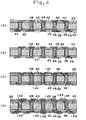
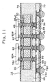
- FIG. 1 is a sectional view of a heat resistant substrate incorporated circuit wiring board according to a first embodiment of the present invention
- FIG. 1 shows the structure of a heat resistant substrate incorporated circuit wiring board of the first embodiment which constitutes a resin made package board.
- the heat resistant substrate incorporated circuit wiring board 10 incorporates a heat resistant substrate 30.
- the heat resistant substrate 30 includes a base material (core substrate) 20.
- the base material 20 contains through hole conductors 36 and through hole pads 38 are formed on both ends of the through hole conductor 36.
- Conductor circuits 39 are formed on both faces of the core substrate 20.
- Via hole conductors 48, conductor circuits 49 and insulator layers 40 and additional wiring layer (built-up wiring layer) comprised of via hole conductors 148, conductor circuits 149 and insulation layers 140 are disposed on both faces of the base material 20.
- Solder resist layer 70 is formed on the front and rear faces of the heat resistant substrate incorporated circuit wiring board 10 and openings 70a are formed in the solder resist layer 70 so as to expose part of the via hole conductor 148 and the conductor circuit 149.
- the exposed portions of the via hole conductor 148 and the conductor circuit 149 correspond to loading pads 148P.
- Solder bumps 78U are provided on the loading pads 148P.
- An IC chip 90 is loaded by connecting electrodes 92 of the IC chip 90 through the solder bumps 78U.
- interlayer resin insulation layer 50 including via hole conductors 60 and conductor circuit 58 and interlayer resin insulation layer 150 including via hole conductors 160 and conductor circuits 158 are disposed on face (bottom face) on the opposite side to the IC chip of the heat resistant substrate 30.
- Solder resist layer 70 is formed on the top layer of the interlayer resin insulation layer 150 and solder bumps 78D are formed in the via hole conductors 160 through the openings 70a in the solder resist layer 70.
- the loading pads 148P are formed just over the via hole conductors 148 and the conductor circuits 149 (other place than just over the via hole conductor 148) extending from the via hole conductors 148.
- the loading pads 148P are disposed in a grid form or a zigzag form and the pitch between the loading pads 148P is set to 30-150 ⁇ m. This pitch is preferred to be 50-100 ⁇ m if considering the insulation property between the loading pads 148P, the reliability of the heat resistant substrate 30 and inclusion of the wiring board of an electronic component into a printed wiring board.
- the pitch of the loading pads 148P in the loading portion is expanded by the built-up layer and this loading pad 148P is conductive with the through hole conductor 36 through conductor circuit (see the conductor circuit 38 on the through hole conductor 36 in FIG. 1 , including the conductor circuit closing the through hole conductor 36) on the core substrate 20.
- the pitch between one through hole conductor 36 and another is larger than the pitch of the loading pads 148P and is set to 30-200 ⁇ m. This is preferred to be 75-150 ⁇ m in views of the insulation reliability of the core substrate 20, heat resistance cycle property and crack resistance property.
- the built-up layer (additional wiring layer on the rear face) is formed on the rear face of the core substrate 20 also and a connecting pad 148D for securing an electric contact with an incorporation wiring substrate incorporating the heat resistant substrate 30 is formed on the rearmost face.
- the pitch of the connecting pads 148D is larger than the pitch of the through hole conductors 36 and is set to 50-250 ⁇ m.
- the connecting pad 148D is formed just over the via hole conductor 148 or on the conductor circuit 149 extending form the via hole conductor 148.
- the via hole conductor 60 for the incorporation wiring substrate is formed on the connecting pad 148D.
- the through hole pads 38 or the conductor circuits 39 on the surface of the base material 20 instead of the loading pads 148P without forming any surface additional wiring layer.
- all the loading pads 148P may be adopted as the through hole pads 38 just over the through hole 36 or the loading pads 148P located in the circumference may be part (see the conductor circuit 39 connected to the through hole conductors 36 on both ends of FIG. 1 ) of the conductor circuit 39 connected to the through hole conductor 36 while the loading pad 148P located in the center may be part of the through hole pad 38 just over the through hole conductor 36.
- the conductor circuit 39 and the through hole pad 38 on the rear face of the base material 20 may be adopted as the connecting pad 148D without forming the rear face additional wiring layer.
- all the connecting pads 148D may be adopted as the through hole pads 38 just over the through hole conductors 36.
- the connecting pads 148D around the core substrate 20 may be adopted as part of the conductor circuit 39 connected to the through hole conductor 36 (see the conductor circuit 39 connected to the through hole conductors 36 on both ends of FIG.1 ) while the connecting pad 148D in the center may be adopted as part of the through hole pad 38 just over the through hole conductor 36.
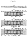
- the heat resistant substrate 30 is preferred to be comprised of the substrate 20 and surface additional wiring layer (surface built-up layer).
- the insulation layer 140 is formed ( FIG. 4(C) ) and the heat resistant substrate 30 is formed by providing the via hole conductor 148 and the conductor circuit 149 ( FIG. 4(D) ).
- the IC chip 90 is loaded by alignment with the heat resistant substrate incorporated circuit wiring board 10. After that, it is installed by reflowing (see FIG. 1 ). Then, sealant (under-fill: not shown) is applied between the heat resistant substrate incorporated circuit wiring board 10 and the IC chip 90 and cured at 80° for 15 minutes and at 150° C for two hours.
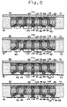
- FIG. 8 shows the structure of the heat resistant substrate incorporated circuit wiring board of the second embodiment.
- the heat resistant substrate incorporated circuit wiring board 10 incorporates the heat resistant substrate 30.
- the heat resistant substrate 30 has the base material 20, the base material 20 is provided with the through hole conductor 36 and the through hole pads 38 are formed on both ends of the through hole conductor 36.
- a built-up wiring layer comprised of the via hole conductor 48 and the insulation layer 40 is disposed on the face (top face) on the side of an IC chip of the heat resistant substrate 30. No additional wiring layer is provided on the rear face.
- the solder bump 78U is provided in the opening 70a of the solder resist layer 70 of the via hole conductor 48.
- An IC chip (MPU) 90A and an IC chip (memory) 90B are loaded by connecting the electrode 92 of the IC chip 90A and IC chip 90B.
- the thickness of the heat resistant substrate incorporated circuit wiring board 10 is 0.1-1.0 mm and the thickness of the core substrate 20 is 0.05-0.5 mm.
- the thermal expansion coefficient of the base material (core base plate) 20 is 3.0-10 ppm and the thermal expansion coefficient of the heat resistant substrate incorporated circuit wiring board 10 can be reduced by means of the base material 20. Stress caused by a difference in thermal expansion between the IC chips 90A, 90B and the resin made heat resistant substrate incorporated circuit wiring board 10 is reduced. As a result, stress applied to the solder bump between the IC chip and resin made package is reduced. Further, no stress is transmitted to the resin of the wiring layer of the IC chip wiring board. Thus, no crack or breaking occurs in the resin of the IC chip wiring layer.
- the structure of the heat resistant substrate incorporated circuit wiring board of the third embodiment will be described with reference to FIG. 9 .
- the additional wiring layers are provided on both faces of the core substrate in the first embodiment described with reference to FIG. 1 . Contrary to this, according to the third embodiment, no additional wiring is provided on its core substrate.
- the structure of the third embodiment also enables the heat resistant substrate incorporated circuit wiring board to be thinned with the core substrate 20 and prevents breaking of wire caused by thermal contraction by bringing the thermal expansion coefficients of the IC chip (chip set) 90A and IC chip (GPLI) 90B and the heat resistant substrate incorporated circuit wiring board 30 close to each other.
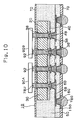
- the structure of the heat resistant substrate incorporated circuit wiring board according to the fourth embodiment will be described with reference to FIG. 10 .
- the additional wiring layers are provided on both faces of the core substrate 20 in the first embodiment described with reference to FIG. 1 .
- a built-up wiring layer is provided on the surface (bottom face) on an opposite side to the IC chip (memory) 90A and the IC chip (logic) 90B of the core substrate 20.
- the structure of the fourth embodiment also can obtain substantially the same effect as the first embodiment.
- the structure of the heat resistant substrate incorporated circuit wiring board according to the fifth embodiment will be described with reference to FIG. 11 .
- the additional wiring layers are provided on both faces of the core substrate 20 in the first embodiment described with reference to FIG. 1 .
- the built-up wiring layers are provided on both the surface (top face) on the IC chip side of the core substrate 20 and the surface (bottom face) on an opposite side to the IC chip.
- the structure of the fifth embodiment enables the thermal expansion coefficient of the heat resistant substrate incorporated circuit wiring board to be reduced although the additional wiring with the heat resistant substrate is not performed.
- the heat resistant substrate 30 is incorporated in the interlayer insulation layer 50 of the heat resistant substrate incorporated circuit wiring board 10.
- the interlayer resin insulation layer 50 of the heat resistant substrate incorporated circuit wiring board and the surface on the IC chip side of the heat resistant substrate 30 are formed into a substantially flat surface without a difference of step. Further, no solder resist layer is provided on the top face.
- the heat resistant substrate 30 is incorporated in the interlayer insulation layer 50 of the heat resistant substrate incorporated circuit wiring board 10. Contrary to this, the surface of the heat resistant substrate 30 is projected from the interlayer resin insulation layer 50 on the front surface of the heat resistant substrate incorporated circuit wiring board. Further, no solder resist layer is provided on the top surface.
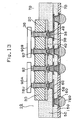
- the structure of the heat resistant substrate incorporated circuit wiring board according to the eighth embodiment will be described with reference to FIG. 14 .
- the built-up layers 50 and 150 of the heat resistant substrate incorporated circuit wiring board are provided on the lower side of the heat resistant substrate 30.
- the built-up wiring layer 150 of the heat resistant substrate incorporated circuit wiring board is formed on the face on the IC chip side of the heat resistant substrate 30.
- the through hole pad 38 and the conductor circuit 39 are formed on the surface of the base material 20 of the heat resistant substrate 30. Contrary to this, the through hole pad 38 and the conductor circuit 39 are provided only on the face on the IC chip side of the base material 20 of the heat resistant substrate 30.
- the through hole pad 38 and the conductor circuit 39 are formed on both faces of the core substrate 20. Contrary to this, according to the tenth embodiment, the through hole pad 38 and the conductor circuit 39 are provided only on the face on an opposite side to the IC chip of the base material 20 of the heat resistant substrate 30.
- the structure of the heat resistant substrate incorporated circuit wiring board according to the eleventh embodiment will be described with reference to FIG. 17 .
- the through hole pad 38 and the conductor circuit 39 are formed on both faces of the core substrate 20.
- no conductor circuit is provided on the base material 20.
- the pitch of the loading pads 148P, the pitch of the through hole conductors 36 and the pitch of the connecting pads 148D are identical.
- the pitch of the loading pads 148P, the pitch of the through hole conductors 36 and the pitch of the connecting pads 148D are larger in this order like the first embodiment described with reference to FIG. 1 .
- a plurality of electronic components are loaded in the second embodiment-eleventh embodiment, it is permissible to provide an MPU on one side while a memory is provided on the other side and provide both sides of the surface wiring layers (surface built-up layers) on the core substrate 20 with wiring for exchanging a signal therebetween.
- chip set, logic, graphic and the like are available.
Landscapes
- Engineering & Computer Science (AREA)
- Microelectronics & Electronic Packaging (AREA)
- Manufacturing & Machinery (AREA)
- Physics & Mathematics (AREA)
- Thermal Sciences (AREA)
- Production Of Multi-Layered Print Wiring Board (AREA)
Applications Claiming Priority (2)
| Application Number | Priority Date | Filing Date | Title |
|---|---|---|---|
| US11/415,117 US7462784B2 (en) | 2006-05-02 | 2006-05-02 | Heat resistant substrate incorporated circuit wiring board |
| PCT/JP2007/058587 WO2007129545A1 (ja) | 2006-05-02 | 2007-04-20 | 耐熱性基板内蔵回路配線板 |
Publications (3)
| Publication Number | Publication Date |
|---|---|
| EP2015623A1 EP2015623A1 (en) | 2009-01-14 |
| EP2015623A4 EP2015623A4 (en) | 2009-12-16 |
| EP2015623B1 true EP2015623B1 (en) | 2012-03-28 |
Family
ID=38660202
Family Applications (1)
| Application Number | Title | Priority Date | Filing Date |
|---|---|---|---|
| EP07742023A Ceased EP2015623B1 (en) | 2006-05-02 | 2007-04-20 | Circuit wiring board incorporating heat resistant substrate |
Country Status (7)
| Country | Link |
|---|---|
| US (5) | US7462784B2 (https=) |
| EP (1) | EP2015623B1 (https=) |
| JP (1) | JPWO2007129545A1 (https=) |
| KR (1) | KR101026655B1 (https=) |
| CN (2) | CN101395978B (https=) |
| TW (2) | TW201121376A (https=) |
| WO (1) | WO2007129545A1 (https=) |
Families Citing this family (108)
| Publication number | Priority date | Publication date | Assignee | Title |
|---|---|---|---|---|
| WO2005107350A1 (ja) * | 2004-04-28 | 2005-11-10 | Ibiden Co., Ltd. | 多層プリント配線板 |
| JP4824397B2 (ja) | 2005-12-27 | 2011-11-30 | イビデン株式会社 | 多層プリント配線板 |
| US7462784B2 (en) * | 2006-05-02 | 2008-12-09 | Ibiden Co., Ltd. | Heat resistant substrate incorporated circuit wiring board |
| AT9551U1 (de) * | 2006-05-16 | 2007-11-15 | Austria Tech & System Tech | Verfahren zum festlegen eines elektronischen bauteils auf einer leiterplatte sowie system bestehend aus einer leiterplatte und wenigstens einem elektronischen bauteil |
| JP5068060B2 (ja) * | 2006-10-30 | 2012-11-07 | 新光電気工業株式会社 | 半導体パッケージおよびその製造方法 |
| US8455766B2 (en) * | 2007-08-08 | 2013-06-04 | Ibiden Co., Ltd. | Substrate with low-elasticity layer and low-thermal-expansion layer |
| JP5085266B2 (ja) * | 2007-10-12 | 2012-11-28 | 富士通株式会社 | 配線基板およびその製造方法 |
| JP5306634B2 (ja) * | 2007-11-22 | 2013-10-02 | 新光電気工業株式会社 | 配線基板及び半導体装置及び配線基板の製造方法 |
| JP5079475B2 (ja) * | 2007-12-05 | 2012-11-21 | 新光電気工業株式会社 | 電子部品実装用パッケージ |
| US8283570B2 (en) * | 2007-12-26 | 2012-10-09 | Panasonic Corporation | Semiconductor assembly and multilayer wiring board |
| JP2009224492A (ja) * | 2008-03-14 | 2009-10-01 | Oki Semiconductor Co Ltd | 半導体装置及びその製造方法 |
| US8130507B2 (en) * | 2008-03-24 | 2012-03-06 | Ngk Spark Plug Co., Ltd. | Component built-in wiring board |
| US8178976B2 (en) * | 2008-05-12 | 2012-05-15 | Texas Instruments Incorporated | IC device having low resistance TSV comprising ground connection |
| JP5378380B2 (ja) * | 2008-07-23 | 2013-12-25 | ルネサスエレクトロニクス株式会社 | 半導体装置及びその製造方法 |
| JP5350745B2 (ja) * | 2008-10-21 | 2013-11-27 | 新光電気工業株式会社 | 配線基板 |
| US8186053B2 (en) * | 2008-11-14 | 2012-05-29 | Fujitsu Limited | Circuit board and method of manufacturing the same |
| TWI384603B (zh) | 2009-02-17 | 2013-02-01 | 日月光半導體製造股份有限公司 | 基板結構及應用其之封裝結構 |
| JP5577760B2 (ja) * | 2009-03-09 | 2014-08-27 | 新光電気工業株式会社 | パッケージ基板および半導体装置の製造方法 |
| US8395054B2 (en) * | 2009-03-12 | 2013-03-12 | Ibiden Co., Ltd. | Substrate for mounting semiconductor element and method for manufacturing substrate for mounting semiconductor element |
| US8829355B2 (en) * | 2009-03-27 | 2014-09-09 | Ibiden Co., Ltd. | Multilayer printed wiring board |
| US7936060B2 (en) * | 2009-04-29 | 2011-05-03 | International Business Machines Corporation | Reworkable electronic device assembly and method |
| JP5249132B2 (ja) * | 2009-06-03 | 2013-07-31 | 新光電気工業株式会社 | 配線基板 |
| JP5532744B2 (ja) * | 2009-08-20 | 2014-06-25 | 富士通株式会社 | マルチチップモジュール及びマルチチップモジュールの製造方法 |
| US8466562B2 (en) * | 2009-09-24 | 2013-06-18 | Headway Technologies, Inc. | Layered chip package |
| JP5290215B2 (ja) * | 2010-02-15 | 2013-09-18 | ルネサスエレクトロニクス株式会社 | 半導体装置、半導体パッケージ、インタポーザ、及びインタポーザの製造方法 |
| JP5115578B2 (ja) * | 2010-03-26 | 2013-01-09 | Tdk株式会社 | 多層配線板及び多層配線板の製造方法 |
| US9048233B2 (en) * | 2010-05-26 | 2015-06-02 | Taiwan Semiconductor Manufacturing Company, Ltd. | Package systems having interposers |
| JP5565949B2 (ja) * | 2010-07-30 | 2014-08-06 | 京セラSlcテクノロジー株式会社 | 配線基板 |
| TWI460834B (zh) * | 2010-08-26 | 2014-11-11 | 欣興電子股份有限公司 | 嵌埋穿孔晶片之封裝結構及其製法 |
| TWI418269B (zh) * | 2010-12-14 | 2013-12-01 | 欣興電子股份有限公司 | 嵌埋穿孔中介層之封裝基板及其製法 |
| KR101767108B1 (ko) * | 2010-12-15 | 2017-08-11 | 삼성전자주식회사 | 하이브리드 기판을 구비하는 반도체 패키지 및 그 제조방법 |
| TWI459520B (zh) * | 2011-01-31 | 2014-11-01 | 精材科技股份有限公司 | 轉接板及其形成方法 |
| US20120217049A1 (en) * | 2011-02-28 | 2012-08-30 | Ibiden Co., Ltd. | Wiring board with built-in imaging device |
| TWI455268B (zh) * | 2011-03-22 | 2014-10-01 | 南亞電路板股份有限公司 | 封裝載板及其製造方法 |
| JP2012204831A (ja) | 2011-03-23 | 2012-10-22 | Ibiden Co Ltd | 電子部品内蔵配線板及びその製造方法 |
| TWI421995B (zh) * | 2011-04-27 | 2014-01-01 | 欣興電子股份有限公司 | 半導體封裝結構及其製法 |
| GB201108425D0 (en) * | 2011-05-19 | 2011-07-06 | Zarlink Semiconductor Inc | Integrated circuit package |
| US8829684B2 (en) | 2011-05-19 | 2014-09-09 | Microsemi Semiconductor Limited | Integrated circuit package |
| US9128123B2 (en) | 2011-06-03 | 2015-09-08 | Taiwan Semiconductor Manufacturing Company, Ltd. | Interposer test structures and methods |
| TWI492680B (zh) | 2011-08-05 | 2015-07-11 | 欣興電子股份有限公司 | 嵌埋有中介層之封裝基板及其製法 |
| US20130068516A1 (en) * | 2011-09-19 | 2013-03-21 | Tessera Research Llc | High io substrates and interposers without vias |
| TWI476888B (zh) * | 2011-10-31 | 2015-03-11 | 欣興電子股份有限公司 | 嵌埋穿孔中介層之封裝基板及其製法 |
| US11127664B2 (en) | 2011-10-31 | 2021-09-21 | Unimicron Technology Corp. | Circuit board and manufacturing method thereof |
| US20130215586A1 (en) * | 2012-02-16 | 2013-08-22 | Ibiden Co., Ltd. | Wiring substrate |
| JP2013214578A (ja) | 2012-03-30 | 2013-10-17 | Ibiden Co Ltd | 配線板及びその製造方法 |
| JP5931547B2 (ja) | 2012-03-30 | 2016-06-08 | イビデン株式会社 | 配線板及びその製造方法 |
| US9236322B2 (en) * | 2012-04-11 | 2016-01-12 | Taiwan Semiconductor Manufacturing Company, Ltd. | Methods and apparatus for heat spreader on silicon |
| JP2013243227A (ja) | 2012-05-18 | 2013-12-05 | Ibiden Co Ltd | 配線板及びその製造方法 |
| FR2991108A1 (fr) * | 2012-05-24 | 2013-11-29 | St Microelectronics Sa | Ligne coplanaire blindee |
| US8901435B2 (en) | 2012-08-14 | 2014-12-02 | Bridge Semiconductor Corporation | Hybrid wiring board with built-in stopper, interposer and build-up circuitry |
| TWM455979U (zh) * | 2012-09-21 | 2013-06-21 | Chunghwa Prec Test Tech Co Ltd | 微小間距測試載板結構 |
| TWI483365B (zh) * | 2012-09-26 | 2015-05-01 | 財團法人工業技術研究院 | 封裝基板及其製法 |
| TWI543307B (zh) | 2012-09-27 | 2016-07-21 | 欣興電子股份有限公司 | 封裝載板與晶片封裝結構 |
| TWI499023B (zh) * | 2012-10-11 | 2015-09-01 | 財團法人工業技術研究院 | 封裝基板及其製法 |
| CN103779284A (zh) * | 2012-10-22 | 2014-05-07 | 欣兴电子股份有限公司 | 封装载板与芯片封装结构 |
| TWI544599B (zh) * | 2012-10-30 | 2016-08-01 | 矽品精密工業股份有限公司 | 封裝結構之製法 |
| US10032696B2 (en) | 2012-12-21 | 2018-07-24 | Nvidia Corporation | Chip package using interposer substrate with through-silicon vias |
| US9312219B2 (en) * | 2012-12-28 | 2016-04-12 | Dyi-chung Hu | Interposer and packaging substrate having the interposer |
| JP2014216377A (ja) * | 2013-04-23 | 2014-11-17 | イビデン株式会社 | 電子部品とその製造方法及び多層プリント配線板の製造方法 |
| TWI503934B (zh) | 2013-05-09 | 2015-10-11 | 日月光半導體製造股份有限公司 | 半導體元件及其製造方法及半導體封裝結構 |
| US8836098B1 (en) * | 2013-05-15 | 2014-09-16 | Freescale Semiconductor, Inc. | Surface mount semiconductor device with solder ball reinforcement frame |
| JP5959562B2 (ja) * | 2013-05-30 | 2016-08-02 | 京セラ株式会社 | 配線基板 |
| JP2014236188A (ja) | 2013-06-05 | 2014-12-15 | イビデン株式会社 | 配線板及びその製造方法 |
| JP2014236187A (ja) | 2013-06-05 | 2014-12-15 | イビデン株式会社 | 配線板及びその製造方法 |
| TWI512923B (zh) * | 2013-06-18 | 2015-12-11 | 矽品精密工業股份有限公司 | 中介板及其製法 |
| JP6161437B2 (ja) * | 2013-07-03 | 2017-07-12 | 新光電気工業株式会社 | 配線基板及びその製造方法、半導体パッケージ |
| KR102192356B1 (ko) * | 2013-07-29 | 2020-12-18 | 삼성전자주식회사 | 반도체 패키지 |
| AT515069B1 (de) * | 2013-11-07 | 2019-10-15 | At & S Austria Tech & Systemtechnik Ag | Leiterplattenstruktur |
| KR102155740B1 (ko) * | 2014-02-21 | 2020-09-14 | 엘지이노텍 주식회사 | 인쇄회로기판 및 이의 제조 방법 |
| US9799622B2 (en) * | 2014-06-18 | 2017-10-24 | Dyi-chung Hu | High density film for IC package |
| JP2016021496A (ja) * | 2014-07-15 | 2016-02-04 | イビデン株式会社 | 配線基板及びその製造方法 |
| US9699921B2 (en) | 2014-08-01 | 2017-07-04 | Fujikura Ltd. | Multi-layer wiring board |
| JP2016035987A (ja) | 2014-08-04 | 2016-03-17 | イビデン株式会社 | 電子部品内蔵配線板及びその製造方法 |
| CN105590914B (zh) * | 2014-10-24 | 2018-04-06 | 碁鼎科技秦皇岛有限公司 | 电子元件封装结构及制作方法 |
| US10306777B2 (en) * | 2014-12-15 | 2019-05-28 | Bridge Semiconductor Corporation | Wiring board with dual stiffeners and dual routing circuitries integrated together and method of making the same |
| US9818684B2 (en) * | 2016-03-10 | 2017-11-14 | Amkor Technology, Inc. | Electronic device with a plurality of redistribution structures having different respective sizes |
| US9659853B2 (en) * | 2015-04-24 | 2017-05-23 | Advanced Semiconductor Engineering, Inc. | Double side via last method for double embedded patterned substrate |
| JP6550260B2 (ja) * | 2015-04-28 | 2019-07-24 | 新光電気工業株式会社 | 配線基板及び配線基板の製造方法 |
| JP6657609B2 (ja) * | 2015-06-12 | 2020-03-04 | 凸版印刷株式会社 | 配線回路基板、半導体装置、配線回路基板の製造方法および半導体装置の製造方法 |
| TW201701429A (zh) * | 2015-06-24 | 2017-01-01 | 華亞科技股份有限公司 | 晶圓級封裝及其製作方法 |
| KR102150555B1 (ko) | 2015-08-12 | 2020-09-01 | 삼성전기주식회사 | 방열부재 및 이를 구비한 인쇄회로기판 |
| KR102498627B1 (ko) * | 2015-10-05 | 2023-02-10 | 엘지이노텍 주식회사 | 인쇄회로기판 및 이를 포함하는 전자 부품 패키지 |
| US9735079B2 (en) * | 2015-10-08 | 2017-08-15 | Dyi-chung Hu | Molding compound wrapped package substrate |
| CN105436645A (zh) * | 2015-12-07 | 2016-03-30 | 天津平高智能电气有限公司 | 一种用于真空开关装配的钎焊方法 |
| US10515899B2 (en) * | 2016-10-03 | 2019-12-24 | Taiwan Semiconductor Manufacturing Co., Ltd. | Package structure with bump |
| JP6744202B2 (ja) * | 2016-12-06 | 2020-08-19 | ルネサスエレクトロニクス株式会社 | 半導体装置 |
| US10002852B1 (en) * | 2016-12-15 | 2018-06-19 | Dyi-chung Hu | Package on package configuration |
| CN106783777A (zh) * | 2016-12-26 | 2017-05-31 | 华进半导体封装先导技术研发中心有限公司 | 芯片封装结构及方法 |
| US10178755B2 (en) * | 2017-05-09 | 2019-01-08 | Unimicron Technology Corp. | Circuit board stacked structure and method for forming the same |
| US10685922B2 (en) * | 2017-05-09 | 2020-06-16 | Unimicron Technology Corp. | Package structure with structure reinforcing element and manufacturing method thereof |
| US10950535B2 (en) | 2017-05-09 | 2021-03-16 | Unimicron Technology Corp. | Package structure and method of manufacturing the same |
| TWI683407B (zh) * | 2017-05-23 | 2020-01-21 | 矽品精密工業股份有限公司 | 基板結構及其製法 |
| US11101186B2 (en) * | 2018-03-16 | 2021-08-24 | Advanced Semiconductor Engineering, Inc. | Substrate structure having pad portions |
| US11640934B2 (en) * | 2018-03-30 | 2023-05-02 | Intel Corporation | Lithographically defined vertical interconnect access (VIA) in dielectric pockets in a package substrate |
| JP7202785B2 (ja) * | 2018-04-27 | 2023-01-12 | 新光電気工業株式会社 | 配線基板及び配線基板の製造方法 |
| JP2019220504A (ja) * | 2018-06-15 | 2019-12-26 | イビデン株式会社 | インダクタ内蔵基板およびその製造方法 |
| CN110875294B (zh) * | 2018-08-29 | 2024-01-23 | 恒劲科技股份有限公司 | 半导体装置的封装结构及其制造方法 |
| CN115547846A (zh) * | 2019-02-21 | 2022-12-30 | 奥特斯科技(重庆)有限公司 | 部件承载件及其制造方法和电气装置 |
| US12205877B2 (en) | 2019-02-21 | 2025-01-21 | AT&S(Chongqing) Company Limited | Ultra-thin component carrier having high stiffness and method of manufacturing the same |
| DE102019107760A1 (de) | 2019-03-26 | 2020-10-01 | OSRAM Opto Semiconductors Gesellschaft mit beschränkter Haftung | Verfahren zur herstellung einer verbindungsstruktur und halbleiterbauelement |
| CN112216688A (zh) * | 2019-07-11 | 2021-01-12 | 苏州旭创科技有限公司 | 一种载板及光模块 |
| US11410934B2 (en) * | 2020-04-16 | 2022-08-09 | Advanced Semiconductor Engineering, Inc. | Substrate and semiconductor device package and method for manufacturing the same |
| CN114007344B (zh) * | 2020-07-28 | 2024-04-12 | 庆鼎精密电子(淮安)有限公司 | 内埋元件电路板的制作方法以及内埋元件电路板 |
| US11355454B2 (en) * | 2020-07-30 | 2022-06-07 | Taiwan Semiconductor Manufacturing Company, Ltd. | Package structure and manufacturing method thereof |
| US12310032B2 (en) * | 2021-06-08 | 2025-05-20 | Intel Corporation | Stacked backend memory with resistive switching devices |
| US20230070053A1 (en) * | 2021-09-09 | 2023-03-09 | Applied Materials, Inc. | Stiffener frame for semiconductor device packages |
| KR20230094341A (ko) | 2021-12-21 | 2023-06-28 | 대덕전자 주식회사 | 패키지기판 |
| CN120345068A (zh) * | 2023-11-16 | 2025-07-18 | 京东方科技集团股份有限公司 | 集成基板及其制备方法、电子设备 |
Citations (1)
| Publication number | Priority date | Publication date | Assignee | Title |
|---|---|---|---|---|
| US20050263867A1 (en) * | 2004-05-28 | 2005-12-01 | Rokuro Kambe | Intermediate substrate |
Family Cites Families (33)
| Publication number | Priority date | Publication date | Assignee | Title |
|---|---|---|---|---|
| FR2567684B1 (fr) * | 1984-07-10 | 1988-11-04 | Nec Corp | Module ayant un substrat ceramique multicouche et un circuit multicouche sur ce substrat et procede pour sa fabrication |
| JP2996510B2 (ja) * | 1990-11-30 | 2000-01-11 | 株式会社日立製作所 | 電子回路基板 |
| JP3754171B2 (ja) | 1997-04-08 | 2006-03-08 | 富士通株式会社 | 回路基板及びその製造方法 |
| JPH11317582A (ja) * | 1998-02-16 | 1999-11-16 | Matsushita Electric Ind Co Ltd | 多層配線基板およびその製造方法 |
| JPH11289025A (ja) * | 1998-04-01 | 1999-10-19 | Ngk Spark Plug Co Ltd | ビルドアップ多層配線基板 |
| JP2000183532A (ja) | 1998-12-16 | 2000-06-30 | Ibiden Co Ltd | プリント配線板 |
| JP3761862B2 (ja) | 1999-05-27 | 2006-03-29 | Hoya株式会社 | 両面配線板の製造方法 |
| JP3756041B2 (ja) | 1999-05-27 | 2006-03-15 | Hoya株式会社 | 多層プリント配線板の製造方法 |
| CN100381027C (zh) * | 1999-09-02 | 2008-04-09 | 伊比登株式会社 | 印刷布线板及其制造方法 |
| JP2001102479A (ja) | 1999-09-27 | 2001-04-13 | Toshiba Corp | 半導体集積回路装置およびその製造方法 |
| JP3585793B2 (ja) * | 1999-11-09 | 2004-11-04 | 富士通株式会社 | 両面薄膜配線基板の製造方法 |
| JP3796099B2 (ja) | 2000-05-12 | 2006-07-12 | 新光電気工業株式会社 | 半導体装置用インターポーザー、その製造方法および半導体装置 |
| JP2002290030A (ja) * | 2001-03-23 | 2002-10-04 | Ngk Spark Plug Co Ltd | 配線基板 |
| JP3612031B2 (ja) | 2001-03-29 | 2005-01-19 | Tdk株式会社 | 高周波モジュール |
| JP2002344142A (ja) | 2001-05-15 | 2002-11-29 | Ibiden Co Ltd | 多層プリント配線板の製造方法 |
| JP2003174250A (ja) | 2001-09-28 | 2003-06-20 | Ibiden Co Ltd | プリント配線板及びプリント配線板の製造方法 |
| JP2003197811A (ja) | 2001-12-27 | 2003-07-11 | Hitachi Ltd | ガラス基板及びその製造方法、並びに配線基板、半導体モジュール |
| JP3666591B2 (ja) | 2002-02-01 | 2005-06-29 | 株式会社トッパンNecサーキットソリューションズ | 半導体チップ搭載用基板の製造方法 |
| US7091589B2 (en) * | 2002-12-11 | 2006-08-15 | Dai Nippon Printing Co., Ltd. | Multilayer wiring board and manufacture method thereof |
| JP2004228521A (ja) * | 2003-01-27 | 2004-08-12 | Ngk Spark Plug Co Ltd | 配線基板およびその製造方法 |
| JP2005033195A (ja) | 2003-06-20 | 2005-02-03 | Ngk Spark Plug Co Ltd | コンデンサ及びコンデンサの製造方法 |
| JP2005039243A (ja) * | 2003-06-24 | 2005-02-10 | Ngk Spark Plug Co Ltd | 中間基板 |
| JP2005032905A (ja) | 2003-07-10 | 2005-02-03 | Ibiden Co Ltd | 多層プリント配線板 |
| US7049170B2 (en) * | 2003-12-17 | 2006-05-23 | Tru-Si Technologies, Inc. | Integrated circuits and packaging substrates with cavities, and attachment methods including insertion of protruding contact pads into cavities |
| JP4504925B2 (ja) | 2004-01-30 | 2010-07-14 | イビデン株式会社 | 多層プリント配線板及びその製造方法 |
| WO2005107350A1 (ja) | 2004-04-28 | 2005-11-10 | Ibiden Co., Ltd. | 多層プリント配線板 |
| TWI242855B (en) * | 2004-10-13 | 2005-11-01 | Advanced Semiconductor Eng | Chip package structure, package substrate and manufacturing method thereof |
| JP4546415B2 (ja) * | 2005-09-01 | 2010-09-15 | 日本特殊陶業株式会社 | 配線基板、セラミックキャパシタ |
| JP4824397B2 (ja) | 2005-12-27 | 2011-11-30 | イビデン株式会社 | 多層プリント配線板 |
| US7462784B2 (en) * | 2006-05-02 | 2008-12-09 | Ibiden Co., Ltd. | Heat resistant substrate incorporated circuit wiring board |
| US7843302B2 (en) | 2006-05-08 | 2010-11-30 | Ibiden Co., Ltd. | Inductor and electric power supply using it |
| US8395054B2 (en) | 2009-03-12 | 2013-03-12 | Ibiden Co., Ltd. | Substrate for mounting semiconductor element and method for manufacturing substrate for mounting semiconductor element |
| US8829355B2 (en) | 2009-03-27 | 2014-09-09 | Ibiden Co., Ltd. | Multilayer printed wiring board |
-
2006
- 2006-05-02 US US11/415,117 patent/US7462784B2/en active Active
-
2007
- 2007-04-17 TW TW099139185A patent/TW201121376A/zh not_active IP Right Cessation
- 2007-04-17 TW TW096113475A patent/TW200810630A/zh unknown
- 2007-04-20 WO PCT/JP2007/058587 patent/WO2007129545A1/ja not_active Ceased
- 2007-04-20 KR KR1020087013649A patent/KR101026655B1/ko active Active
- 2007-04-20 CN CN2007800071626A patent/CN101395978B/zh active Active
- 2007-04-20 CN CN201110360635.9A patent/CN102497723B/zh active Active
- 2007-04-20 EP EP07742023A patent/EP2015623B1/en not_active Ceased
- 2007-04-20 JP JP2008514421A patent/JPWO2007129545A1/ja active Pending
-
2008
- 2008-12-08 US US12/330,147 patent/US8008583B2/en not_active Expired - Lifetime
-
2009
- 2009-06-19 US US12/488,207 patent/US7994432B2/en not_active Expired - Lifetime
- 2009-06-19 US US12/488,224 patent/US8507806B2/en not_active Expired - Lifetime
-
2010
- 2010-11-23 US US12/952,759 patent/US8541691B2/en not_active Expired - Lifetime
Patent Citations (1)
| Publication number | Priority date | Publication date | Assignee | Title |
|---|---|---|---|---|
| US20050263867A1 (en) * | 2004-05-28 | 2005-12-01 | Rokuro Kambe | Intermediate substrate |
Also Published As
| Publication number | Publication date |
|---|---|
| CN102497723A (zh) | 2012-06-13 |
| US7462784B2 (en) | 2008-12-09 |
| US20090260857A1 (en) | 2009-10-22 |
| TWI347154B (https=) | 2011-08-11 |
| CN101395978A (zh) | 2009-03-25 |
| US8008583B2 (en) | 2011-08-30 |
| CN102497723B (zh) | 2014-11-05 |
| KR101026655B1 (ko) | 2011-04-04 |
| KR20080087085A (ko) | 2008-09-30 |
| CN101395978B (zh) | 2013-02-06 |
| WO2007129545A1 (ja) | 2007-11-15 |
| US20070256858A1 (en) | 2007-11-08 |
| US20090084594A1 (en) | 2009-04-02 |
| JPWO2007129545A1 (ja) | 2009-09-17 |
| TW201121376A (en) | 2011-06-16 |
| EP2015623A1 (en) | 2009-01-14 |
| US8541691B2 (en) | 2013-09-24 |
| EP2015623A4 (en) | 2009-12-16 |
| US8507806B2 (en) | 2013-08-13 |
| TW200810630A (en) | 2008-02-16 |
| US20090255716A1 (en) | 2009-10-15 |
| US20110063806A1 (en) | 2011-03-17 |
| TWI358973B (https=) | 2012-02-21 |
| US7994432B2 (en) | 2011-08-09 |
Similar Documents
| Publication | Publication Date | Title |
|---|---|---|
| EP2015623B1 (en) | Circuit wiring board incorporating heat resistant substrate | |
| US8003896B2 (en) | Multi-layer printed wiring board and manufacturing method thereof | |
| US8418360B2 (en) | Method for manufacturing a printed wiring board | |
| US7957154B2 (en) | Multilayer printed circuit board | |
| JP3050807B2 (ja) | 多層プリント配線板 | |
| TWI246753B (en) | Package substrate for electrolytic leadless plating and manufacturing method thereof | |
| JP3050812B2 (ja) | 多層プリント配線板 | |
| EP1137332A1 (en) | Printed wiring board and method of producing the same and capacitor to be contained in printed wiring board | |
| US20080308308A1 (en) | Method of manufacturing wiring board, method of manufacturing semiconductor device and wiring board | |
| US8592691B2 (en) | Printed wiring board | |
| US8410374B2 (en) | Printed wiring board | |
| JP2004327940A (ja) | 配線基板及びその製造方法 | |
| JP2004111544A (ja) | 多層配線基板 | |
| JP4181149B2 (ja) | 半導体パッケージ | |
| JP2004327939A (ja) | 配線基板及びその製造方法 | |
| JP2006222257A (ja) | 配線基板とその製造方法、およびそれを用いた半導体装置 | |
| JP4560920B2 (ja) | 半導体装置用基板 |
Legal Events
| Date | Code | Title | Description |
|---|---|---|---|
| PUAI | Public reference made under article 153(3) epc to a published international application that has entered the european phase |
Free format text: ORIGINAL CODE: 0009012 |
|
| 17P | Request for examination filed |
Effective date: 20080519 |
|
| AK | Designated contracting states |
Kind code of ref document: A1 Designated state(s): AT BE BG CH CY CZ DE DK EE ES FI FR GB GR HU IE IS IT LI LT LU LV MC MT NL PL PT RO SE SI SK TR |
|
| AX | Request for extension of the european patent |
Extension state: AL BA HR MK RS |
|
| RBV | Designated contracting states (corrected) |
Designated state(s): DE GB |
|
| A4 | Supplementary search report drawn up and despatched |
Effective date: 20091117 |
|
| 17Q | First examination report despatched |
Effective date: 20100305 |
|
| RIC1 | Information provided on ipc code assigned before grant |
Ipc: H05K 3/46 20060101AFI20110728BHEP |
|
| GRAP | Despatch of communication of intention to grant a patent |
Free format text: ORIGINAL CODE: EPIDOSNIGR1 |
|
| DAX | Request for extension of the european patent (deleted) | ||
| GRAS | Grant fee paid |
Free format text: ORIGINAL CODE: EPIDOSNIGR3 |
|
| GRAA | (expected) grant |
Free format text: ORIGINAL CODE: 0009210 |
|
| AK | Designated contracting states |
Kind code of ref document: B1 Designated state(s): DE GB |
|
| REG | Reference to a national code |
Ref country code: GB Ref legal event code: FG4D |
|
| REG | Reference to a national code |
Ref country code: DE Ref legal event code: R096 Ref document number: 602007021622 Country of ref document: DE Effective date: 20120524 |
|
| PLBE | No opposition filed within time limit |
Free format text: ORIGINAL CODE: 0009261 |
|
| STAA | Information on the status of an ep patent application or granted ep patent |
Free format text: STATUS: NO OPPOSITION FILED WITHIN TIME LIMIT |
|
| GBPC | Gb: european patent ceased through non-payment of renewal fee |
Effective date: 20120628 |
|
| 26N | No opposition filed |
Effective date: 20130103 |
|
| REG | Reference to a national code |
Ref country code: DE Ref legal event code: R097 Ref document number: 602007021622 Country of ref document: DE Effective date: 20130103 |
|
| PG25 | Lapsed in a contracting state [announced via postgrant information from national office to epo] |
Ref country code: GB Free format text: LAPSE BECAUSE OF NON-PAYMENT OF DUE FEES Effective date: 20120628 |
|
| PGFP | Annual fee paid to national office [announced via postgrant information from national office to epo] |
Ref country code: DE Payment date: 20170411 Year of fee payment: 11 |
|
| REG | Reference to a national code |
Ref country code: DE Ref legal event code: R119 Ref document number: 602007021622 Country of ref document: DE |
|
| PG25 | Lapsed in a contracting state [announced via postgrant information from national office to epo] |
Ref country code: DE Free format text: LAPSE BECAUSE OF NON-PAYMENT OF DUE FEES Effective date: 20181101 |