JP4824397B2 - 多層プリント配線板 - Google Patents
多層プリント配線板 Download PDFInfo
- Publication number
- JP4824397B2 JP4824397B2 JP2005373733A JP2005373733A JP4824397B2 JP 4824397 B2 JP4824397 B2 JP 4824397B2 JP 2005373733 A JP2005373733 A JP 2005373733A JP 2005373733 A JP2005373733 A JP 2005373733A JP 4824397 B2 JP4824397 B2 JP 4824397B2
- Authority
- JP
- Japan
- Prior art keywords
- pitch
- hole conductors
- hole
- conductor
- processor core
- Prior art date
- Legal status (The legal status is an assumption and is not a legal conclusion. Google has not performed a legal analysis and makes no representation as to the accuracy of the status listed.)
- Expired - Lifetime
Links
Images


Classifications
-
- H—ELECTRICITY
- H10—SEMICONDUCTOR DEVICES; ELECTRIC SOLID-STATE DEVICES NOT OTHERWISE PROVIDED FOR
- H10W—GENERIC PACKAGES, INTERCONNECTIONS, CONNECTORS OR OTHER CONSTRUCTIONAL DETAILS OF DEVICES COVERED BY CLASS H10
- H10W70/00—Package substrates; Interposers; Redistribution layers [RDL]
- H10W70/60—Insulating or insulated package substrates; Interposers; Redistribution layers
- H10W70/62—Insulating or insulated package substrates; Interposers; Redistribution layers characterised by their interconnections
- H10W70/65—Shapes or dispositions of interconnections
-
- H—ELECTRICITY
- H05—ELECTRIC TECHNIQUES NOT OTHERWISE PROVIDED FOR
- H05K—PRINTED CIRCUITS; CASINGS OR CONSTRUCTIONAL DETAILS OF ELECTRIC APPARATUS; MANUFACTURE OF ASSEMBLAGES OF ELECTRICAL COMPONENTS
- H05K3/00—Apparatus or processes for manufacturing printed circuits
- H05K3/46—Manufacturing multilayer circuits
-
- H—ELECTRICITY
- H05—ELECTRIC TECHNIQUES NOT OTHERWISE PROVIDED FOR
- H05K—PRINTED CIRCUITS; CASINGS OR CONSTRUCTIONAL DETAILS OF ELECTRIC APPARATUS; MANUFACTURE OF ASSEMBLAGES OF ELECTRICAL COMPONENTS
- H05K1/00—Printed circuits
- H05K1/02—Details
- H05K1/11—Printed elements for providing electric connections to or between printed circuits
- H05K1/111—Pads for surface mounting, e.g. lay-out
- H05K1/112—Pads for surface mounting, e.g. lay-out directly combined with via connections
- H05K1/113—Via provided in pad; Pad over filled via
-
- H—ELECTRICITY
- H05—ELECTRIC TECHNIQUES NOT OTHERWISE PROVIDED FOR
- H05K—PRINTED CIRCUITS; CASINGS OR CONSTRUCTIONAL DETAILS OF ELECTRIC APPARATUS; MANUFACTURE OF ASSEMBLAGES OF ELECTRICAL COMPONENTS
- H05K1/00—Printed circuits
- H05K1/02—Details
- H05K1/11—Printed elements for providing electric connections to or between printed circuits
- H05K1/115—Via connections; Lands around holes or via connections
-
- H—ELECTRICITY
- H10—SEMICONDUCTOR DEVICES; ELECTRIC SOLID-STATE DEVICES NOT OTHERWISE PROVIDED FOR
- H10W—GENERIC PACKAGES, INTERCONNECTIONS, CONNECTORS OR OTHER CONSTRUCTIONAL DETAILS OF DEVICES COVERED BY CLASS H10
- H10W70/00—Package substrates; Interposers; Redistribution layers [RDL]
- H10W70/60—Insulating or insulated package substrates; Interposers; Redistribution layers
- H10W70/62—Insulating or insulated package substrates; Interposers; Redistribution layers characterised by their interconnections
- H10W70/63—Vias, e.g. via plugs
- H10W70/635—Through-vias
-
- H—ELECTRICITY
- H05—ELECTRIC TECHNIQUES NOT OTHERWISE PROVIDED FOR
- H05K—PRINTED CIRCUITS; CASINGS OR CONSTRUCTIONAL DETAILS OF ELECTRIC APPARATUS; MANUFACTURE OF ASSEMBLAGES OF ELECTRICAL COMPONENTS
- H05K2201/00—Indexing scheme relating to printed circuits covered by H05K1/00
- H05K2201/03—Conductive materials
- H05K2201/0332—Structure of the conductor
- H05K2201/0335—Layered conductors or foils
- H05K2201/0352—Differences between the conductors of different layers of a multilayer
-
- H—ELECTRICITY
- H05—ELECTRIC TECHNIQUES NOT OTHERWISE PROVIDED FOR
- H05K—PRINTED CIRCUITS; CASINGS OR CONSTRUCTIONAL DETAILS OF ELECTRIC APPARATUS; MANUFACTURE OF ASSEMBLAGES OF ELECTRICAL COMPONENTS
- H05K2201/00—Indexing scheme relating to printed circuits covered by H05K1/00
- H05K2201/09—Shape and layout
- H05K2201/09209—Shape and layout details of conductors
- H05K2201/095—Conductive through-holes or vias
- H05K2201/09536—Buried plated through-holes, i.e. plated through-holes formed in a core before lamination
-
- H—ELECTRICITY
- H05—ELECTRIC TECHNIQUES NOT OTHERWISE PROVIDED FOR
- H05K—PRINTED CIRCUITS; CASINGS OR CONSTRUCTIONAL DETAILS OF ELECTRIC APPARATUS; MANUFACTURE OF ASSEMBLAGES OF ELECTRICAL COMPONENTS
- H05K2201/00—Indexing scheme relating to printed circuits covered by H05K1/00
- H05K2201/09—Shape and layout
- H05K2201/09209—Shape and layout details of conductors
- H05K2201/095—Conductive through-holes or vias
- H05K2201/096—Vertically aligned vias, holes or stacked vias
-
- H—ELECTRICITY
- H05—ELECTRIC TECHNIQUES NOT OTHERWISE PROVIDED FOR
- H05K—PRINTED CIRCUITS; CASINGS OR CONSTRUCTIONAL DETAILS OF ELECTRIC APPARATUS; MANUFACTURE OF ASSEMBLAGES OF ELECTRICAL COMPONENTS
- H05K2201/00—Indexing scheme relating to printed circuits covered by H05K1/00
- H05K2201/10—Details of components or other objects attached to or integrated in a printed circuit board
- H05K2201/10613—Details of electrical connections of non-printed components, e.g. special leads
- H05K2201/10621—Components characterised by their electrical contacts
- H05K2201/10674—Flip chip
-
- H—ELECTRICITY
- H05—ELECTRIC TECHNIQUES NOT OTHERWISE PROVIDED FOR
- H05K—PRINTED CIRCUITS; CASINGS OR CONSTRUCTIONAL DETAILS OF ELECTRIC APPARATUS; MANUFACTURE OF ASSEMBLAGES OF ELECTRICAL COMPONENTS
- H05K3/00—Apparatus or processes for manufacturing printed circuits
- H05K3/46—Manufacturing multilayer circuits
- H05K3/4602—Manufacturing multilayer circuits characterized by a special circuit board as base or central core whereon additional circuit layers are built or additional circuit boards are laminated
-
- H—ELECTRICITY
- H05—ELECTRIC TECHNIQUES NOT OTHERWISE PROVIDED FOR
- H05K—PRINTED CIRCUITS; CASINGS OR CONSTRUCTIONAL DETAILS OF ELECTRIC APPARATUS; MANUFACTURE OF ASSEMBLAGES OF ELECTRICAL COMPONENTS
- H05K3/00—Apparatus or processes for manufacturing printed circuits
- H05K3/46—Manufacturing multilayer circuits
- H05K3/4644—Manufacturing multilayer circuits by building the multilayer layer by layer, i.e. build-up multilayer circuits
- H05K3/4652—Adding a circuit layer by laminating a metal foil or a preformed metal foil pattern
-
- H—ELECTRICITY
- H10—SEMICONDUCTOR DEVICES; ELECTRIC SOLID-STATE DEVICES NOT OTHERWISE PROVIDED FOR
- H10W—GENERIC PACKAGES, INTERCONNECTIONS, CONNECTORS OR OTHER CONSTRUCTIONAL DETAILS OF DEVICES COVERED BY CLASS H10
- H10W70/00—Package substrates; Interposers; Redistribution layers [RDL]
- H10W70/60—Insulating or insulated package substrates; Interposers; Redistribution layers
- H10W70/67—Insulating or insulated package substrates; Interposers; Redistribution layers characterised by their insulating layers or insulating parts
- H10W70/68—Shapes or dispositions thereof
- H10W70/685—Shapes or dispositions thereof comprising multiple insulating layers
-
- H—ELECTRICITY
- H10—SEMICONDUCTOR DEVICES; ELECTRIC SOLID-STATE DEVICES NOT OTHERWISE PROVIDED FOR
- H10W—GENERIC PACKAGES, INTERCONNECTIONS, CONNECTORS OR OTHER CONSTRUCTIONAL DETAILS OF DEVICES COVERED BY CLASS H10
- H10W90/00—Package configurations
- H10W90/701—Package configurations characterised by the relative positions of pads or connectors relative to package parts
- H10W90/721—Package configurations characterised by the relative positions of pads or connectors relative to package parts of bump connectors
- H10W90/724—Package configurations characterised by the relative positions of pads or connectors relative to package parts of bump connectors between a chip and a stacked insulating package substrate, interposer or RDL
-
- Y—GENERAL TAGGING OF NEW TECHNOLOGICAL DEVELOPMENTS; GENERAL TAGGING OF CROSS-SECTIONAL TECHNOLOGIES SPANNING OVER SEVERAL SECTIONS OF THE IPC; TECHNICAL SUBJECTS COVERED BY FORMER USPC CROSS-REFERENCE ART COLLECTIONS [XRACs] AND DIGESTS
- Y10—TECHNICAL SUBJECTS COVERED BY FORMER USPC
- Y10T—TECHNICAL SUBJECTS COVERED BY FORMER US CLASSIFICATION
- Y10T29/00—Metal working
- Y10T29/49—Method of mechanical manufacture
- Y10T29/49002—Electrical device making
- Y10T29/49117—Conductor or circuit manufacturing
- Y10T29/49124—On flat or curved insulated base, e.g., printed circuit, etc.
- Y10T29/4913—Assembling to base an electrical component, e.g., capacitor, etc.
- Y10T29/49139—Assembling to base an electrical component, e.g., capacitor, etc. by inserting component lead or terminal into base aperture
Landscapes
- Engineering & Computer Science (AREA)
- Microelectronics & Electronic Packaging (AREA)
- Manufacturing & Machinery (AREA)
- Production Of Multi-Layered Print Wiring Board (AREA)
- Structures For Mounting Electric Components On Printed Circuit Boards (AREA)
Description
そこで、本発明は、実装されたICチップの誤動作が生じ難い半導体素子実装用の多層プリント配線板を提供することを目的とする。
スルーホール導体を有するコア基板上に、導体回路と絶縁性樹脂層とが交互に積層されてなるビルドアップ配線層が形成され、そのビルドアップ配線層の表層にICチップ等の半導体素子(以下、単に「IC」という)を搭載するための実装部を有してなる多層プリント配線板において、
前記ICを実装する領域の直下の領域に配設されるスルーホール導体のピッチを、他の領域に配設されるスルーホール導体のピッチよりも小さくした多層プリント配線板である。
Bc/Tc<(Bp−Bc)/(Tp−Tc)
の関係式で表されるように、IC搭載用パッドとスルーホール導体とを配置することができる。
Pc<Pm≦Ps
の関係式で表されるようなスルーホール導体の配置密度とする。即ち、スルーホール導体の配置密度が、ICのプロセッサコア部直下の領域から、プロセッサコア部直下以外の領域に向かって次第に小さくなるように、スルーホール導体を配設する。
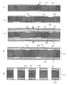
本発明にかかる半導体素子実装用の多層プリント配線板の一実施形態は、図1に示されるように、コア基板を貫通して複数のスルーホール導体が形成され、そのコア基板上に導体回路と絶縁性樹脂層とが交互に積層されてなるビルドアップ配線層が形成され、そのビルドアップ配線層の表層にICを搭載するための実装部を有する多層プリント配線板であって、半導体素子を実装する領域の直下に配設されたスルーホール導体のピッチを、半導体素子を実装する領域以外の他の領域、即ち、半導体素子実装領域の外側の周辺領域に位置するスルーホール導体のピッチよりも挟ピッチとしたことを特徴とする。
Bc/Tc<(Bp−Bc)/(Tp−Tc)
の関係式で表されるように、パッドとスルーホール導体とを配置することが望ましい。
Pc<Pm≦Ps
のような関係式で表されるようなスルーホール導体の配置密度とすることができる、即ち、スルーホール導体の配置密度が、ICのプロセッサコア部直下の領域から、プロセッサコア部直下以外の領域に向かって次第に小さくなるように、スルーホール導体を配設することが望ましい。
配線長を短くできるので、ICへの電源供給の遅延をさらに抑えることができるからである。
40μmを超えると、基板上に形成されるビルドアップ配線層の平坦性が劣るからである。
なお、レーザ加工における照射レーザ光の吸収効率を高めるために、予め絶縁性樹脂基板上の金属箔に公知の黒化処理を施しておくことが望ましい。
上記無電解めっきまたは電解めっきとしては、たとえば、銅、すず、銀、各種はんだ、銅/すず、銅/銀等の金属めっきが好ましく、とくに、無電解銅めっきまたは電解銅めっきが好適である。
この導体回路形成工程は、先ず、前記導体層の表面に感光性ドライフィルムレジストを貼付した後、所定の回路パターンに沿って露光、現像処理してエッチングレジストを形成し、エッチングレジスト非形成部分の導体層をエッチングして、電極パッドを含んだ導体回路パターンとする。
また前記導体層をエッチングして導体回路を形成する前処理として、ファインパターンを形成しやすくするため、あらかじめ、導体層の表面全面をエッチングして厚さを1〜10μm、より好ましくは2〜8μm程度まで薄くすることができる。
A.貫通孔充填用樹脂組成物の調製
ビスフェノールF型エポキシモノマー(油化シェル社製、分子量:310、YL983U)100重量部、表面にシランカップリング剤がコーティングされた平均粒径が1.6μmで、最大粒子の直径が15μm以下のSiO2
球状粒子(アドテック社製、CRS 1101−CE)170重量部およびレベリング剤(サンノプコ社製 ペレノールS4)1.5重量部を容器にとり、攪拌混合することにより、その粘度が23±1℃で44〜49Pa・sの樹脂充填材を調製した。なお、硬化剤として、イミダゾール硬化剤(四国化成社製、2E4MZ−CN)6.5重量部を用いた。スルーホール導体を形成する貫通孔を充填するための樹脂としては、他のエポキシ樹脂(例えば、ビスフェノールA型、ノボラック型など)、ポリイミド樹脂、フェノール樹脂などの熱硬化性樹脂を用いてもよい。
多層コア基板の作成
(1) 厚さ0.6mmのガラスエポキシ樹脂またはBT(ビスマレイミドトリアジン)樹脂からなる絶縁性基板14の両面に、10〜250μmの銅箔16がラミネートされてなる両面銅張積層板10を出発材料として用いた(図2(a))。この実施例1では、30μmの銅箔を使用した。
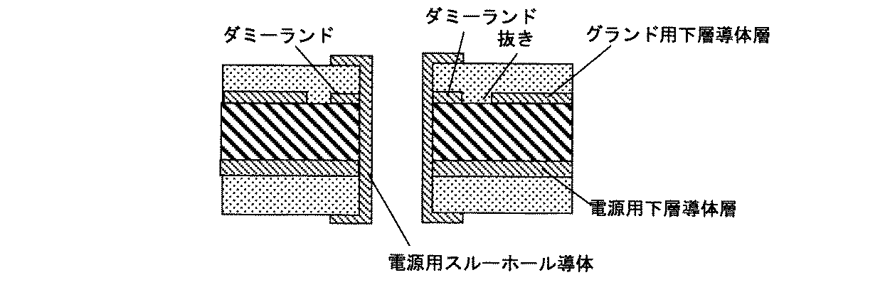
通常、ダミーランドは、スルーホール導体の口径に対して150〜250μm程度大きな口径を有して形成されるので、ダミーランドを有しない導体回路とすることで、ダミーランドを有する通常の構造に比べて、スルーホール導体間および電源用スルーホール導体とグランド用導体層間、グランド用スルーホール導体と電源用導体層間の間隔を狭くすることができる。ここで、ダミーランドとは、図5に示すように、多層コア基板の内層において、スルーホール導体から延出して、抜き22内に配設されたスルーホール周りの導体回路のことである。
このようにダミーランドを設けないことで、相互インダクタンスを減少させたり、導体抵抗を低くすることが可能になる。さらに、電源層、グランド層を構成する導体層の体積を増加させることも可能である。
(6g/l)を含む水溶液を還元浴とする還元処理を行い、下層のグランド用導体層16E、下層の電源用導体層16Pの表面に粗化面を形成する。
なお、表層の導体層に信号用導体回路を形成してもよい。
ここで、実装するICのプロッセサコア部直下の領域に設ける貫通孔35は、100μmφのドリルを用いて、それらのピッチがICの電極ピッチ(パッドピッチ)と同等な125μmとなるように形成される。
また、IC直下でプロセッサコア部以外の領域に設ける貫通孔35は、100μmφのドリルを用いて、それらのピッチが150〜400μmとなるように形成される。
また、IC直下以外の領域に設ける貫通孔35は、250μmφのドリルを用いて、それらのピッチが300〜600μmとなるように形成される。なお、IC直下以外の領域のプリント配線板全体に亘るように形成する。
さらに、ICのプロセッサコア部直下以外に設けるスルーホール導体の個数は、プロセッサコア部直下以外に位置するパッドの個数に対して、10〜50%の割合で形成することが出来るが、本実施例では30%とした。
なお、これらのスルーホール導体36は、信号用スルーホール導体(図示を省略)や、電源用スルーホール導体36P1(100μm)およびグランド用スルーホール導体36E1(100μm)、電源用スルーホール導体36P2(100μm)およびグランド用スルーホール導体36E2(100μm)、電源用スルーホール導体36P3(250μm)およびグランド用スルーホール導体36E3(250μm)から構成される。
ここで、電源用スルーホール導体とグランド用スルーホール導体とを隣接して格子状または千鳥状に配置することが望ましい。プロセッサコア直下のみの電源用スルーホール導体とグランド用スルーホール導体とを隣接して格子状または千鳥状に配置してもよい。なお、符号36P1および36E1で示されるのが、プロセッサコア直下の領域に設けたスルーホール導体である。
(6g/l)を含む水溶液を黒化浴(酸化浴)とする黒化処理、および、NaOH(10g/l)、NaBH4 (6g/l)を含む水溶液を還元浴とする還元処理を行い、スルーホール導体36の内壁に粗化面(図示を省略)を形成する。
その基板30の表面を、研磨して平坦化し、100℃で1時間、150℃で1時間の加熱を行うことにより、貫通孔充填用樹脂組成物40を硬化させて樹脂充填材層を形成した。その後、基板表面(貫通孔充填用樹脂表面も含む)に、無電解めっきおよび電解めっきを施して、多層コア基板の表面および裏面に導体層46、46を形成した(図3(b)参照)。
これにより、多層コア基板30の外側に設ける導体層46は、多層コア基板の内部に設ける導体層16に比べて微細な回路を形成することが可能になり、スルーホールランドの小径化および導体回路間の隙間やスルーホールランドと導体回路との間の隙間を小さくできる。従って、多層コア基板30の表面および裏面側に設けるスルーホールランドや導体回路は、スルーホール導体の挟ピッチ化を阻害することがない。
エッチング液としては、イミダゾール銅(II)錯体10重量部、グリコール酸7.3重量部、塩化カリウム5重量部からなるエッチング液(メック社製、メックエッチボンド)を使用した。
導体回路およびスルーホール導体のランド表面を覆う導体層(ふためっき層)36Lの表面に粗化層を形成すると、その導体は、層間樹脂絶縁層との密着性に優れるので、導体回路およびスルーホール導体のランドを被覆する導体の側面と樹脂絶縁層との界面を起点とするクラックの発生を抑制できる。また一方で、スルーホール導体のランドを覆う導体層は、電気的に接続されるバイアホールとの密着性が改善される。
すなわち、層間絶縁層用樹脂フィルムを基板上に、真空度67Pa、圧力0.47MPa、温度85℃、圧着時間60秒の条件で本圧着し、その後、170℃で40分間熱硬化させた(図3(d)参照)。
この実施例では、直径60μmと75μmの開口50aを形成した。
さらに、粗面化処理(粗化深さ3μm)した該基板の表面に、パラジウム触媒を付与することにより、層間絶縁層の表面およびバイアホール用開口の内壁面に触媒核を付着させた。すなわち、上記基板を塩化パラジウム(PbCl2
)と塩化第一スズ(SnCl2 )とを含む触媒液中に浸漬し、パラジウム金属を析出させることにより触媒を付与した。
〔無電解銅めっき水溶液〕
EDTA 0.200 mol/l
硫酸銅 0.032 mol/l
HCHO 0.1 g/l
NaOH 0.100 mol/l
α、α′−ビピリジル 100 mg/l
ポリエチレングリコール(PEG) 0.10 g/l
〔無電解めっき条件〕
液温度: 34℃
時間: 45分
〔電解銅めっき液〕
硫酸 200 g/l
硫酸銅 80 g/l
添加剤 19.5 ml/l
(アトテックジャパン社製、カパラシドGL)
〔電解めっき条件〕
電流密度 1 A/dm2
時間 70 分
温度 22±2 ℃
次に、ジエチレングリコールジメチルエーテル(DMDG)に60重量%の濃度になるように溶解させた、クレゾールノボラック型エポキシ樹脂(日本化薬社製)のエポキシ基50%をアクリル化した感光性付与のオリゴマー(分子量:4000)45.67重量部、メチルエチルケトンに溶解させた80重量%のビスフェノールA型エポキシ樹脂(油化シェル社製、商品名:エピコート1001)16.0重量部、イミダゾール硬化剤(四国化成社製、商品名:2E4MZ−CN)1.6重量部、感光性モノマーである2官能アクリルモノマー(日本化薬社製、商品名:R604)4.5重量部、同じく多価アクリルモノマー(共栄化学社製、商品名:DPE6A)1.5重量部、分散系消泡剤(サンノプコ社製、S−65)0.71重量部を容器にとり、攪拌、混合して混合組成物を調製し、この混合組成物に対して光重合開始剤としてベンゾフェノン(関東化学社製)1.8重量部、光増感剤としてのミヒラーケトン(関東化学社製)0.2重量部、を加えることにより、粘度を25℃で2.0Pa・sに調整したソルダーレジスト組成物を得た。
なお、粘度測定は、B型粘度計(東京計器社製、DVL−B型)で60min-1の場合はローターNo.4、6min-1の場合はローターNo.3によった。
の紫外線で露光し、DMTG溶液で現像処理し、200μmの直径の開口を形成した。
そして、さらに、80℃で1時間、100℃で1時間、120℃で1時間、150℃で3時間の条件でそれぞれ加熱処理を行ってソルダーレジスト層を硬化させ、開口を有し、その厚さが15〜25μmのソルダーレジストパターン層76を形成した。上記ソルダーレジスト組成物としては、市販のソルダーレジスト組成物を使用することもできる。
そして、この多層プリント配線板には、はんだバンプ78Uを介してプリント配線板に形成されたIC搭載用のパッドとIC80の電極が接続され、さらに、はんだバンプ78Dを介してドータボード82に実装される(図4(c))。
実施例1の(5)の工程において、スルーホール導体を形成するピッチを変更した。プロセッサコア部直下においては、全パッド直下にスルーホール導体を形成することは行わず(プロセッサコア部直下のパッド数に対して50〜100%の範囲内で可能)、1個置きにスルーホール導体を形成したため、250μmピッチとなった。プロセッサコア部直下以外は、プロセッサコア部直下以外のパッド数に対し、10%のスルーホール導体を300〜600μmピッチで形成した。それ以外は実施例1と同様にして多層プリント配線板を作製した。
実施例1の(5)の工程において、スルーホール導体を形成する貫通孔数を変更した。プロセッサコア部直下は、実施例1と同様である。プロセッサコア部直下以外は、プロセッサコア部直下以外のパッド数に対し、50%のスルーホール導体を形成した。プロセッサコア部直下以外のICチップ直下は150〜400μmピッチで、IC直下以外は300〜600μmピッチでスルーホール導体を形成した。それ以外は実施例1と同様にして多層プリント配線板を作製した。
実施例1の(1)の工程において、銅箔16に60μmの銅箔を使用した以外は、実施例1と同様に作製した。
実施例1の(1)の工程において、銅箔16に150μmの銅箔を使用した以外は、実施例1と同様にして多層プリント配線板を作製した。
実施例1において、プロセッサコア部直下以外のスルーホール導体の数を変更した以外は、実施例1と同様にして多層プリント配線板を作製した。この実施例では、実施例2の如く、プロセッサコア直下以外のスルーホール導体の数は、プロセッサコア直下以外のパッド数に対して10%であるように形成した。
プロセッサコア部直下以外の領域に設けたスルーホール導体数を、10%から30%に変更した以外は、実施例2と同様にして多層プリント配線板を作製した。
実施例1の(1)の工程において、銅箔16に20μmの銅箔を使用した以外は、実施例1と同様にして多層プリント配線板を作製した。
実施例1の(1)の工程において、銅箔16に300μmの銅箔を使用した以外は、実施例1と同様に作製した。
実施例1の(5)の工程において、スルーホール導体を形成するドリル及びピッチを変更した。全スルーホール導体を0.1mmΦのドリルを用い、全パッド直下に125μmピッチでスルーホール導体を形成した以外は、実施例1と同様にして多層プリント配線板を作製した。
参考例1において、スルーホール導体を形成するピッチを変更した。プロセッサコア部直下は全パッド直下にスルーホール導体を形成せず、1個置きに形成したため、250μmピッチでスルーホール導体を形成した。IC直下でプロセッサコア部直下以外が全バンプ直下に125μmピッチでスルーホール導体を形成した。
実施例1〜9及び参考例1〜2で作製したそれぞれのプリント配線板に、表1に示すような駆動周波数およびFSB(フロントサイド・バス)を有する3種類のIC(以下、「ICチップNo.1〜No.3」という)のいずれかを搭載し、同時スイッチングを繰り返して、例えば、パルス・パターン・ジェネレータ/エラー・ディテクタ(例えば、アドバンテスト社製:商品名「D3186/3286」)を用いて誤動作の有無を確認する。その結果を表2に示す。誤動作が観察されなかった場合を○、誤動作が観察された場合を×と評価する。
実施例1〜7で作製したそれぞれのプリント配線板に、表1に示すNo.3のICを搭載し、同時スイッチングを繰り返して、ICのトランジスタの電圧降下量を測定する。なお、ICのトランジスタの電圧は直接測定が困難なので、プリント配線板に測定可能な回路を形成して行なう。
14 樹脂絶縁層
16 銅箔
16E グランド用下層導体層
16P 電源用下層導体層
18 プリプレグ
20 銅箔
22 抜き孔
30 コア基板
35 貫通孔
36E1〜36E3 グランド用スルーホール導体
36P1〜36P3 電源用スルーホール導体
40 貫通孔充填用樹脂組成物
46E グランド用導体層
46P 電源用導体層
50 層間樹脂絶縁層
50a バイアホール形成用開口
58 導体回路
60 バイアホール
70 層間樹脂絶縁層
72 導体回路
74 バイアホール
76 ソルダーレジスト層
78U、78D はんだバンプ
80 ICチップ
82 ドータボード
Claims (7)
- スルーホール導体を有するコア基板上に、導体回路と絶縁性樹脂層とが交互に積層されてなるビルドアップ配線層が形成され、そのビルドアップ配線層の表層にIC等の半導体素子を搭載するための実装部を有する多層プリント配線板において、
前記半導体素子を実装する領域の直下に位置するスルーホール導体のピッチを、他の領域に位置するスルーホール導体のピッチよりも小さくするとともに、
前記半導体素子のプロセッサコア部直下に位置するスルーホール導体のピッチを、それ以外のスルーホール導体のピッチよりも小さくし、
前記半導体素子のプロセッサコア部直下の領域に配設されたスルーホール導体のピッチをPcとし、半導体素子を実装する領域の直下であるがプロセッサコア部直下以外の領域に設けたスルーホール導体のピッチをPm、半導体素子を実装する領域以外に設けたスルーホール導体のピッチをPsとするとき、
Pc<Pm≦Ps
の関係式で表されるような配置密度としたことを特徴とする多層プリント配線板。 - 前記半導体素子のプロセッサコア部直下に配設する半導体素子搭載用のパッドの数をBc、プロセッサコア部直下の領域に配設するスルーホール導体の数をTcとし、
全てのパッド数および全てのスルーホール導体の数をそれぞれBpおよびTpとするとき、
Bc/Tc<(Bp−Bc)/(Tp−Tc)
の関係式で表されるように、パッドとスルーホール導体とが配設されることを特徴とする請求項1に記載の多層プリント配線板。 - 前記半導体素子のプロセッサコア部直下の領域に配設されるスルーホール導体のピッチは、125〜250μmであることを特徴とする請求項1または2に記載の多層プリント配線板。
- 前記半導体素子を実装する領域の直下であるが、プロセッサコア部直下以外の領域に設けるスルーホール導体のピッチは、150〜600μmピッチであることを特徴とする請求項1から3までのいずれか1項に記載の多層プリント配線板。
- 前記半導体素子を実装する領域の直下以外に設けるスルーホール導体のピッチは、200〜600μmであることを特徴とする請求項1から4までのいずれか1項に記載の多層プリント配線板。
- 前記半導体子素子のプロセッサコア部直下の領域に設けたスルーホール導体のピッチと、プロセッサコア部直下に設けたパッドのピッチが一致していることを特徴とする請求項1から5までのいずれか1項に記載の多層プリント配線板。
- 前記コア基板は、コア材上に導体回路と絶縁性樹脂層とが交互に積層されてなる多層コア基板であり、前記多層コア基板の内部に設けた導体回路の厚みをTとし、多層コア基板の表面に設けた導体回路の厚みをtとするとき、T≧1.5tであることを特徴とする請求項1から6までのいずれか1項に記載の多層プリント配線板。
Priority Applications (10)
| Application Number | Priority Date | Filing Date | Title |
|---|---|---|---|
| JP2005373733A JP4824397B2 (ja) | 2005-12-27 | 2005-12-27 | 多層プリント配線板 |
| CN2010102453328A CN101916752B (zh) | 2005-12-27 | 2006-12-27 | 多层印刷线路板 |
| KR1020087005431A KR100978774B1 (ko) | 2005-12-27 | 2006-12-27 | 다층 프린트 배선판 |
| CN2006800362256A CN101278392B (zh) | 2005-12-27 | 2006-12-27 | 多层印刷线路板 |
| TW100114816A TW201141344A (en) | 2005-12-27 | 2006-12-27 | Multilayer printed wiring board |
| TW095149141A TWI387424B (zh) | 2005-12-27 | 2006-12-27 | Multilayer printed wiring board |
| EP06843746A EP1968113A4 (en) | 2005-12-27 | 2006-12-27 | MULTILAYER CONDUCTOR PLATE |
| PCT/JP2006/326376 WO2007074941A1 (ja) | 2005-12-27 | 2006-12-27 | 多層プリント配線板 |
| US12/163,286 US7781681B2 (en) | 2005-12-27 | 2008-06-27 | Multilayer printed wiring board |
| US12/842,431 US8334466B2 (en) | 2005-12-27 | 2010-07-23 | Multilayer printed wiring board |
Applications Claiming Priority (1)
| Application Number | Priority Date | Filing Date | Title |
|---|---|---|---|
| JP2005373733A JP4824397B2 (ja) | 2005-12-27 | 2005-12-27 | 多層プリント配線板 |
Publications (2)
| Publication Number | Publication Date |
|---|---|
| JP2007180076A JP2007180076A (ja) | 2007-07-12 |
| JP4824397B2 true JP4824397B2 (ja) | 2011-11-30 |
Family
ID=38218157
Family Applications (1)
| Application Number | Title | Priority Date | Filing Date |
|---|---|---|---|
| JP2005373733A Expired - Lifetime JP4824397B2 (ja) | 2005-12-27 | 2005-12-27 | 多層プリント配線板 |
Country Status (7)
| Country | Link |
|---|---|
| US (2) | US7781681B2 (ja) |
| EP (1) | EP1968113A4 (ja) |
| JP (1) | JP4824397B2 (ja) |
| KR (1) | KR100978774B1 (ja) |
| CN (2) | CN101278392B (ja) |
| TW (2) | TW201141344A (ja) |
| WO (1) | WO2007074941A1 (ja) |
Families Citing this family (31)
| Publication number | Priority date | Publication date | Assignee | Title |
|---|---|---|---|---|
| WO2005107350A1 (ja) * | 2004-04-28 | 2005-11-10 | Ibiden Co., Ltd. | 多層プリント配線板 |
| JP4824397B2 (ja) * | 2005-12-27 | 2011-11-30 | イビデン株式会社 | 多層プリント配線板 |
| US7462784B2 (en) * | 2006-05-02 | 2008-12-09 | Ibiden Co., Ltd. | Heat resistant substrate incorporated circuit wiring board |
| JPWO2010134511A1 (ja) * | 2009-05-20 | 2012-11-12 | 日本電気株式会社 | 半導体装置及び半導体装置の製造方法 |
| US8624127B2 (en) | 2010-02-26 | 2014-01-07 | Ibiden Co., Ltd. | Wiring board and method for manufacturing the same |
| US9532444B2 (en) | 2010-02-26 | 2016-12-27 | Mitsubishi Electric Corporation | Method of manufacturing printed wiring board, and printed wiring board |
| US9048233B2 (en) * | 2010-05-26 | 2015-06-02 | Taiwan Semiconductor Manufacturing Company, Ltd. | Package systems having interposers |
| JP5775747B2 (ja) * | 2011-06-03 | 2015-09-09 | 新光電気工業株式会社 | 配線基板及びその製造方法 |
| JP5730152B2 (ja) * | 2011-07-26 | 2015-06-03 | 京セラサーキットソリューションズ株式会社 | 配線基板 |
| US20130062210A1 (en) * | 2011-09-13 | 2013-03-14 | Hoya Corporation | Manufacturing method of substrate and manufacturing method of wiring substrate |
| JP5797534B2 (ja) * | 2011-11-24 | 2015-10-21 | 京セラサーキットソリューションズ株式会社 | 配線基板 |
| WO2013168761A1 (ja) * | 2012-05-10 | 2013-11-14 | 日立化成株式会社 | 多層配線基板 |
| CN102711394B (zh) * | 2012-06-25 | 2016-02-24 | 广州美维电子有限公司 | 一种用于电路板的电镀互连加工工艺 |
| WO2014050081A1 (ja) * | 2012-09-25 | 2014-04-03 | 株式会社デンソー | 電子装置 |
| CN103153002B (zh) * | 2013-02-21 | 2016-04-13 | 广州兴森快捷电路科技有限公司 | 具有三面包夹孔铜结构印制电路板的制造方法 |
| JP6013960B2 (ja) * | 2013-03-28 | 2016-10-25 | 京セラ株式会社 | 配線基板 |
| JP5894221B2 (ja) * | 2014-06-11 | 2016-03-23 | 京セラ株式会社 | インターポーザー、それを用いた実装構造体及び電子機器 |
| CN104141904B (zh) * | 2014-07-22 | 2017-12-05 | 上海博恩世通光电股份有限公司 | 一种插入式双面固晶全周发光led功率型灯丝模组 |
| US9325536B2 (en) | 2014-09-19 | 2016-04-26 | Dell Products, Lp | Enhanced receiver equalization |
| US9317649B2 (en) | 2014-09-23 | 2016-04-19 | Dell Products, Lp | System and method of determining high speed resonance due to coupling from broadside layers |
| US9313056B1 (en) | 2014-11-07 | 2016-04-12 | Dell Products, Lp | System aware transmitter adaptation for high speed serial interfaces |
| TWI605733B (zh) * | 2016-11-10 | 2017-11-11 | 南亞電路板股份有限公司 | 電路板及其製造方法 |
| JP6263286B1 (ja) * | 2017-01-13 | 2018-01-17 | 日本特殊陶業株式会社 | スパークプラグの製造方法 |
| KR20190041215A (ko) * | 2017-10-12 | 2019-04-22 | 주식회사 아모그린텍 | 인쇄회로기판 제조 방법 및 이에 의해 제조된 인쇄회로기판 |
| JP6984442B2 (ja) | 2018-01-25 | 2021-12-22 | 富士通株式会社 | 基板、電子装置、及び基板の設計支援方法 |
| JP7209740B2 (ja) * | 2018-12-25 | 2023-01-20 | 京セラ株式会社 | 電子部品実装用基板および電子装置 |
| US20200343271A1 (en) * | 2019-04-29 | 2020-10-29 | Innolux Corporation | Electronic device |
| WO2021142599A1 (zh) * | 2020-01-14 | 2021-07-22 | 深圳市大疆创新科技有限公司 | 一种芯片封装结构及封装方法 |
| US11956898B2 (en) * | 2020-09-23 | 2024-04-09 | Apple Inc. | Three-dimensional (3D) copper in printed circuit boards |
| WO2023153754A1 (ko) * | 2022-02-09 | 2023-08-17 | 삼성전자 주식회사 | 인터포저를 포함하는 전자 장치 및 그 제조 방법 |
| KR102737071B1 (ko) * | 2024-01-02 | 2024-12-03 | 엘지이노텍 주식회사 | 회로기판 및 이를 포함하는 반도체 패키지 기판 |
Family Cites Families (30)
| Publication number | Priority date | Publication date | Assignee | Title |
|---|---|---|---|---|
| US5543661A (en) * | 1994-05-31 | 1996-08-06 | Sumitomo Metal Ceramics Inc. | Semiconductor ceramic package with terminal vias |
| JPH11289025A (ja) * | 1998-04-01 | 1999-10-19 | Ngk Spark Plug Co Ltd | ビルドアップ多層配線基板 |
| US6613986B1 (en) * | 1998-09-17 | 2003-09-02 | Ibiden Co., Ltd. | Multilayer build-up wiring board |
| US6333857B1 (en) * | 1998-12-25 | 2001-12-25 | Ngk Spark Plug Co., Ltd. | Printing wiring board, core substrate, and method for fabricating the core substrate |
| US6538213B1 (en) * | 2000-02-18 | 2003-03-25 | International Business Machines Corporation | High density design for organic chip carriers |
| US6534852B1 (en) * | 2000-04-11 | 2003-03-18 | Advanced Semiconductor Engineering, Inc. | Ball grid array semiconductor package with improved strength and electric performance and method for making the same |
| JP2002374066A (ja) | 2001-06-14 | 2002-12-26 | Ibiden Co Ltd | 多層プリント配線板の製造方法 |
| US6566761B1 (en) * | 2002-05-03 | 2003-05-20 | Applied Micro Circuits Corporation | Electronic device package with high speed signal interconnect between die pad and external substrate pad |
| KR101162522B1 (ko) * | 2003-04-07 | 2012-07-09 | 이비덴 가부시키가이샤 | 다층프린트배선판 |
| JP2005033176A (ja) * | 2003-06-20 | 2005-02-03 | Ngk Spark Plug Co Ltd | コンデンサ及びコンデンサの製造方法 |
| US6885541B2 (en) * | 2003-06-20 | 2005-04-26 | Ngk Spark Plug Co., Ltd. | Capacitor, and capacitor manufacturing process |
| JP2005033195A (ja) * | 2003-06-20 | 2005-02-03 | Ngk Spark Plug Co Ltd | コンデンサ及びコンデンサの製造方法 |
| US8021748B2 (en) * | 2003-09-29 | 2011-09-20 | Ibiden Co., Ltd. | Interlayer insulating layer for printed wiring board, printed wiring board and method for manufacturing same |
| WO2005074340A1 (ja) * | 2004-01-30 | 2005-08-11 | Ibiden Co., Ltd. | 多層プリント配線板及びその製造方法 |
| JP4291729B2 (ja) * | 2004-04-23 | 2009-07-08 | 新光電気工業株式会社 | 基板及び半導体装置 |
| WO2005107350A1 (ja) * | 2004-04-28 | 2005-11-10 | Ibiden Co., Ltd. | 多層プリント配線板 |
| JP4521223B2 (ja) * | 2004-05-21 | 2010-08-11 | イビデン株式会社 | プリント配線板 |
| WO2005117510A1 (ja) * | 2004-05-27 | 2005-12-08 | Ibiden Co., Ltd. | 多層プリント配線板 |
| JP2006024698A (ja) * | 2004-07-07 | 2006-01-26 | Toshiba Corp | 半導体装置及びその製造方法 |
| JP3979405B2 (ja) * | 2004-07-13 | 2007-09-19 | セイコーエプソン株式会社 | 電気光学装置、実装構造体及び電子機器 |
| DE102004047753B4 (de) * | 2004-09-30 | 2009-01-02 | Advanced Micro Devices, Inc., Sunnyvale | Verbesserte Chip-Kontaktierungsanordnung für Chip-Träger für Flip-Chip-Anwendungen |
| US8164920B2 (en) * | 2005-06-13 | 2012-04-24 | Ibiden Co., Ltd. | Printed wiring board |
| JP4546415B2 (ja) * | 2005-09-01 | 2010-09-15 | 日本特殊陶業株式会社 | 配線基板、セラミックキャパシタ |
| US7742314B2 (en) * | 2005-09-01 | 2010-06-22 | Ngk Spark Plug Co., Ltd. | Wiring board and capacitor |
| JP4824397B2 (ja) * | 2005-12-27 | 2011-11-30 | イビデン株式会社 | 多層プリント配線板 |
| US7462784B2 (en) * | 2006-05-02 | 2008-12-09 | Ibiden Co., Ltd. | Heat resistant substrate incorporated circuit wiring board |
| US7843302B2 (en) * | 2006-05-08 | 2010-11-30 | Ibiden Co., Ltd. | Inductor and electric power supply using it |
| US7616470B2 (en) * | 2006-06-16 | 2009-11-10 | International Business Machines Corporation | Method for achieving very high bandwidth between the levels of a cache hierarchy in 3-dimensional structures, and a 3-dimensional structure resulting therefrom |
| US8395054B2 (en) * | 2009-03-12 | 2013-03-12 | Ibiden Co., Ltd. | Substrate for mounting semiconductor element and method for manufacturing substrate for mounting semiconductor element |
| US8829355B2 (en) * | 2009-03-27 | 2014-09-09 | Ibiden Co., Ltd. | Multilayer printed wiring board |
-
2005
- 2005-12-27 JP JP2005373733A patent/JP4824397B2/ja not_active Expired - Lifetime
-
2006
- 2006-12-27 CN CN2006800362256A patent/CN101278392B/zh active Active
- 2006-12-27 KR KR1020087005431A patent/KR100978774B1/ko active Active
- 2006-12-27 TW TW100114816A patent/TW201141344A/zh unknown
- 2006-12-27 WO PCT/JP2006/326376 patent/WO2007074941A1/ja not_active Ceased
- 2006-12-27 CN CN2010102453328A patent/CN101916752B/zh active Active
- 2006-12-27 EP EP06843746A patent/EP1968113A4/en not_active Withdrawn
- 2006-12-27 TW TW095149141A patent/TWI387424B/zh active
-
2008
- 2008-06-27 US US12/163,286 patent/US7781681B2/en active Active
-
2010
- 2010-07-23 US US12/842,431 patent/US8334466B2/en active Active
Also Published As
| Publication number | Publication date |
|---|---|
| JP2007180076A (ja) | 2007-07-12 |
| CN101278392B (zh) | 2010-09-29 |
| TW201141344A (en) | 2011-11-16 |
| EP1968113A1 (en) | 2008-09-10 |
| WO2007074941A8 (ja) | 2009-08-27 |
| US20100288544A1 (en) | 2010-11-18 |
| CN101278392A (zh) | 2008-10-01 |
| TWI387424B (zh) | 2013-02-21 |
| CN101916752A (zh) | 2010-12-15 |
| TW200742524A (en) | 2007-11-01 |
| US20090000812A1 (en) | 2009-01-01 |
| CN101916752B (zh) | 2012-08-22 |
| KR100978774B1 (ko) | 2010-08-30 |
| US8334466B2 (en) | 2012-12-18 |
| US7781681B2 (en) | 2010-08-24 |
| EP1968113A4 (en) | 2012-06-13 |
| WO2007074941A1 (ja) | 2007-07-05 |
| KR20080038204A (ko) | 2008-05-02 |
Similar Documents
| Publication | Publication Date | Title |
|---|---|---|
| JP4824397B2 (ja) | 多層プリント配線板 | |
| JP4488684B2 (ja) | 多層プリント配線板 | |
| US6828510B1 (en) | Multilayer printed wiring board and method of manufacturing multilayer printed wiring board | |
| WO2005076683A1 (ja) | 多層プリント配線板 | |
| JP4947121B2 (ja) | 多層プリント配線板 | |
| JP4592889B2 (ja) | 多層回路基板 | |
| JP2002271040A (ja) | 多層プリント配線板の製造方法 | |
| JP4566335B2 (ja) | 多層プリント配線板 | |
| JP2001244636A (ja) | プリント配線板 | |
| JP2002204057A (ja) | 多層プリント配線板の製造方法および多層プリント配線板 | |
| JP2001237510A (ja) | プリント配線板 | |
| JP4475930B2 (ja) | 多層プリント配線板 | |
| JP4514308B2 (ja) | 多層プリント配線板の製造方法 | |
| JP2001244635A (ja) | プリント配線板の製造方法 | |
| JP3219396B2 (ja) | 多層プリント配線板の製造方法 | |
| JP2010166099A (ja) | プリント配線板及びプリント配線板の製造方法 | |
| JP4873827B2 (ja) | 多層プリント配線板 | |
| JP2003008239A (ja) | 多層プリント配線板 | |
| JP4428783B2 (ja) | プリント配線板の製造方法 | |
| JP3219395B2 (ja) | 多層プリント配線板の製造方法 | |
| JP2001177254A (ja) | スルーホールの充填方法および多層プリント配線板の製造方法 | |
| JP4518660B2 (ja) | 多層プリント配線板の製造方法 | |
| JP2001094262A (ja) | プリント配線板、ポリオレフィン系樹脂組成物およびプリント配線板の製造方法 | |
| JP2004079554A (ja) | 片面回路基板およびその製造方法 | |
| JP2002134889A (ja) | プリント配線板の製造方法 |
Legal Events
| Date | Code | Title | Description |
|---|---|---|---|
| A621 | Written request for application examination |
Free format text: JAPANESE INTERMEDIATE CODE: A621 Effective date: 20081120 |
|
| A131 | Notification of reasons for refusal |
Free format text: JAPANESE INTERMEDIATE CODE: A131 Effective date: 20110531 |
|
| A521 | Request for written amendment filed |
Free format text: JAPANESE INTERMEDIATE CODE: A523 Effective date: 20110727 |
|
| TRDD | Decision of grant or rejection written | ||
| A01 | Written decision to grant a patent or to grant a registration (utility model) |
Free format text: JAPANESE INTERMEDIATE CODE: A01 Effective date: 20110830 |
|
| A01 | Written decision to grant a patent or to grant a registration (utility model) |
Free format text: JAPANESE INTERMEDIATE CODE: A01 |
|
| A61 | First payment of annual fees (during grant procedure) |
Free format text: JAPANESE INTERMEDIATE CODE: A61 Effective date: 20110908 |
|
| R150 | Certificate of patent or registration of utility model |
Ref document number: 4824397 Country of ref document: JP Free format text: JAPANESE INTERMEDIATE CODE: R150 Free format text: JAPANESE INTERMEDIATE CODE: R150 |
|
| FPAY | Renewal fee payment (event date is renewal date of database) |
Free format text: PAYMENT UNTIL: 20140916 Year of fee payment: 3 |
|
| R250 | Receipt of annual fees |
Free format text: JAPANESE INTERMEDIATE CODE: R250 |
|
| R250 | Receipt of annual fees |
Free format text: JAPANESE INTERMEDIATE CODE: R250 |
|
| R250 | Receipt of annual fees |
Free format text: JAPANESE INTERMEDIATE CODE: R250 |
|
| R250 | Receipt of annual fees |
Free format text: JAPANESE INTERMEDIATE CODE: R250 |
|
| R250 | Receipt of annual fees |
Free format text: JAPANESE INTERMEDIATE CODE: R250 |
|
| R250 | Receipt of annual fees |
Free format text: JAPANESE INTERMEDIATE CODE: R250 |
|
| R250 | Receipt of annual fees |
Free format text: JAPANESE INTERMEDIATE CODE: R250 |
|
| R250 | Receipt of annual fees |
Free format text: JAPANESE INTERMEDIATE CODE: R250 |
|
| R250 | Receipt of annual fees |
Free format text: JAPANESE INTERMEDIATE CODE: R250 |
|
| R250 | Receipt of annual fees |
Free format text: JAPANESE INTERMEDIATE CODE: R250 |
|
| EXPY | Cancellation because of completion of term |