EP0693779B1 - Resin sealing type semiconductor device and method of making the same - Google Patents
Resin sealing type semiconductor device and method of making the same Download PDFInfo
- Publication number
- EP0693779B1 EP0693779B1 EP95109655A EP95109655A EP0693779B1 EP 0693779 B1 EP0693779 B1 EP 0693779B1 EP 95109655 A EP95109655 A EP 95109655A EP 95109655 A EP95109655 A EP 95109655A EP 0693779 B1 EP0693779 B1 EP 0693779B1
- Authority
- EP
- European Patent Office
- Prior art keywords
- lead
- element mounting
- frame
- semiconductor element
- leads
- Prior art date
- Legal status (The legal status is an assumption and is not a legal conclusion. Google has not performed a legal analysis and makes no representation as to the accuracy of the status listed.)
- Expired - Lifetime
Links
Images







Classifications
-
- H—ELECTRICITY
- H10—SEMICONDUCTOR DEVICES; ELECTRIC SOLID-STATE DEVICES NOT OTHERWISE PROVIDED FOR
- H10W—GENERIC PACKAGES, INTERCONNECTIONS, CONNECTORS OR OTHER CONSTRUCTIONAL DETAILS OF DEVICES COVERED BY CLASS H10
- H10W40/00—Arrangements for thermal protection or thermal control
- H10W40/70—Fillings or auxiliary members in containers or in encapsulations for thermal protection or control
- H10W40/77—Auxiliary members characterised by their shape
- H10W40/778—Auxiliary members characterised by their shape in encapsulations
-
- H—ELECTRICITY
- H10—SEMICONDUCTOR DEVICES; ELECTRIC SOLID-STATE DEVICES NOT OTHERWISE PROVIDED FOR
- H10W—GENERIC PACKAGES, INTERCONNECTIONS, CONNECTORS OR OTHER CONSTRUCTIONAL DETAILS OF DEVICES COVERED BY CLASS H10
- H10W74/00—Encapsulations, e.g. protective coatings
- H10W74/10—Encapsulations, e.g. protective coatings characterised by their shape or disposition
- H10W74/111—Encapsulations, e.g. protective coatings characterised by their shape or disposition the semiconductor body being completely enclosed
- H10W74/121—Encapsulations, e.g. protective coatings characterised by their shape or disposition the semiconductor body being completely enclosed by multiple encapsulations, e.g. by a thin protective coating and a thick encapsulation
-
- H—ELECTRICITY
- H10—SEMICONDUCTOR DEVICES; ELECTRIC SOLID-STATE DEVICES NOT OTHERWISE PROVIDED FOR
- H10W—GENERIC PACKAGES, INTERCONNECTIONS, CONNECTORS OR OTHER CONSTRUCTIONAL DETAILS OF DEVICES COVERED BY CLASS H10
- H10W72/00—Interconnections or connectors in packages
- H10W72/50—Bond wires
- H10W72/541—Dispositions of bond wires
- H10W72/5449—Dispositions of bond wires not being orthogonal to a side surface of the chip, e.g. fan-out arrangements
-
- H—ELECTRICITY
- H10—SEMICONDUCTOR DEVICES; ELECTRIC SOLID-STATE DEVICES NOT OTHERWISE PROVIDED FOR
- H10W—GENERIC PACKAGES, INTERCONNECTIONS, CONNECTORS OR OTHER CONSTRUCTIONAL DETAILS OF DEVICES COVERED BY CLASS H10
- H10W72/00—Interconnections or connectors in packages
- H10W72/50—Bond wires
- H10W72/551—Materials of bond wires
- H10W72/552—Materials of bond wires comprising metals or metalloids, e.g. silver
-
- H—ELECTRICITY
- H10—SEMICONDUCTOR DEVICES; ELECTRIC SOLID-STATE DEVICES NOT OTHERWISE PROVIDED FOR
- H10W—GENERIC PACKAGES, INTERCONNECTIONS, CONNECTORS OR OTHER CONSTRUCTIONAL DETAILS OF DEVICES COVERED BY CLASS H10
- H10W72/00—Interconnections or connectors in packages
- H10W72/50—Bond wires
- H10W72/551—Materials of bond wires
- H10W72/552—Materials of bond wires comprising metals or metalloids, e.g. silver
- H10W72/5522—Materials of bond wires comprising metals or metalloids, e.g. silver comprising gold [Au]
-
- H—ELECTRICITY
- H10—SEMICONDUCTOR DEVICES; ELECTRIC SOLID-STATE DEVICES NOT OTHERWISE PROVIDED FOR
- H10W—GENERIC PACKAGES, INTERCONNECTIONS, CONNECTORS OR OTHER CONSTRUCTIONAL DETAILS OF DEVICES COVERED BY CLASS H10
- H10W72/00—Interconnections or connectors in packages
- H10W72/90—Bond pads, in general
- H10W72/931—Shapes of bond pads
- H10W72/932—Plan-view shape, i.e. in top view
-
- H—ELECTRICITY
- H10—SEMICONDUCTOR DEVICES; ELECTRIC SOLID-STATE DEVICES NOT OTHERWISE PROVIDED FOR
- H10W—GENERIC PACKAGES, INTERCONNECTIONS, CONNECTORS OR OTHER CONSTRUCTIONAL DETAILS OF DEVICES COVERED BY CLASS H10
- H10W74/00—Encapsulations, e.g. protective coatings
-
- H—ELECTRICITY
- H10—SEMICONDUCTOR DEVICES; ELECTRIC SOLID-STATE DEVICES NOT OTHERWISE PROVIDED FOR
- H10W—GENERIC PACKAGES, INTERCONNECTIONS, CONNECTORS OR OTHER CONSTRUCTIONAL DETAILS OF DEVICES COVERED BY CLASS H10
- H10W74/00—Encapsulations, e.g. protective coatings
- H10W74/10—Encapsulations, e.g. protective coatings characterised by their shape or disposition
- H10W74/111—Encapsulations, e.g. protective coatings characterised by their shape or disposition the semiconductor body being completely enclosed
- H10W74/127—Encapsulations, e.g. protective coatings characterised by their shape or disposition the semiconductor body being completely enclosed characterised by arrangements for sealing or adhesion
-
- H—ELECTRICITY
- H10—SEMICONDUCTOR DEVICES; ELECTRIC SOLID-STATE DEVICES NOT OTHERWISE PROVIDED FOR
- H10W—GENERIC PACKAGES, INTERCONNECTIONS, CONNECTORS OR OTHER CONSTRUCTIONAL DETAILS OF DEVICES COVERED BY CLASS H10
- H10W90/00—Package configurations
- H10W90/701—Package configurations characterised by the relative positions of pads or connectors relative to package parts
- H10W90/751—Package configurations characterised by the relative positions of pads or connectors relative to package parts of bond wires
- H10W90/756—Package configurations characterised by the relative positions of pads or connectors relative to package parts of bond wires between a chip and a stacked lead frame, conducting package substrate or heat sink
Definitions
- the invention relates to a semiconductor device characterized by lead construction and a method of making the same.
- VLSIs Very Large Scale Integrated Circuits
- pads for signal input and output on the chip and also a large number of power supply electrodes. This therefore requires a similarly large number of leads for connecting the electrodes.
- JP 4-174551 discloses a semiconductor device that is designed to solve the foregoing problem.
- This semiconductor device provides a common inner lead laminated on the semiconductor chip circuit formation surface with an insulating adhesive.
- a plurality of inner signal leads is provided around the semiconductor chip, electrically connected to the semiconductor chip. Further, the semiconductor chip is sealed by molding resin while supported by the common inner lead.
- This semiconductor device has advantages in that since no tab is provided to mount the semiconductor chip thereupon, tab to bonding wire shorting can be prevented, by using the common inner lead for power supply, the sharing of lead pins can be simply implemented.
- the provision of the common inner lead not only reduces the number of leads, but also reduces the voltage drop by shortening the wires.
- JP 6-66351 discloses a semiconductor device in which a common inner lead is provided around a semiconductor chip.
- the common inner lead is not provided on the surface of the semiconductor chip, thus there are no restrictions on the arrangement of the pads on the semiconductor chip surface. Bonding deficiencies also are avoided.
- the tab on which the semiconductor chip is mounted is provided integrally on one lead, and the common inner lead is provided around this tab, it is difficult to ensure adequate insulation between the tab and the common inner lead.
- the common inner lead is formed in such a manner that one portion is cut off to avoid contacting the lead on which the tab is formed, and thus, placing restrictions on the design. Furthermore, such restrictions places further restrictions on the position at which the bonding is performed.
- This invention provides a heat radiator with high thermal conductivity having such a structure that an element may be mounted thereon in place of a die pad.
- the inner leads are supported by an insulating material disposed on the heat radiator.
- a resin sealing type semiconductor device according to the pre-characterizing portion of claim 1 is disclosed in the document KARMEZOS M. ET AL: "EDQUAD - AN ENHANCED PERFORMANCE PLASTIC PACKAGE", 1 May 1994, PROCEEDINGS OF THE ELECTRONIC COMPONENTS AND TECHNOLOGY CONFERENCE, WASHINGTON, MAY 1-4, 1994, NR. CONF.44, PAGE(S) 63-66, INSTITUTE OF ELECTRICAL AND ELECTRONICS ENGINEERS XP000479147.
- the lead frame is constituted by four seperate sections located at positions of said semiconductor element corresponding to the four corners of that element. Some of the inner lead portions are connected to respective sections of this lead frame by which the flexibility of arranging and using the leads is decreased.
- JP-A-05 190721 discloses a resin sealing type semiconductor device having an element mounting member supporting a semiconductor element and a plurality of electrode members disposed below the element mounting member and one below the other.
- a plurality of wires including first wires electrically connecting a first number of inner lead portions to a first number of electrodes of said semiconductor element, second wires electrically connecting a second number of inner lead portions to said electrode members, and third wires electrically connecting said electrode members to a second number of electrodes of said semiconductor element are provided.
- a resin member seals the element mounting member, the semiconductor element, the plurality of wires, the electrode members and said inner lead portions while exposing outer lead portions.
- the inner lead portions are not supported other than by being embedded in the resin member.
- JP-A-06 151485 discloses a resin sealing type semiconductor device having a wiring board formed on a metallic substrate and a plurality of leads stuck to the board by means of an insulating bonding agent.
- the semiconductor device is mounted on the metallic substrate in the center thereof, and a plurality of wires are used for connecting the leads to the semiconductor device.
- JP-A-06053346 discloses a resin sealing type semiconductor device having a lead which connects a semiconductor chip with an external circuit board. One end of the lead is connected to the power source connecting pad of the semiconductor chip and the other end is connected to the external circuit board.
- the device comprises a substrate where a conductive pattern for connecting the semiconductor chip with the external circuit board is formed separately from the lead. A resin member seals the semiconductor chip and the substrate.
- the object of the invention is to provide a resin sealing type semiconductor device and a fabrication method thereof, enabling highly flexible wire arrangement design by making leads common so as to reduce the number of leads and the voltage drop with shortened wires.
- Another object of the invention is to provide a resin sealing type semiconductor device which has good heat radiation efficiency and a fabrication method thereof.
- the resin sealing type semiconductor device of the invention comprises an element mounting member having an element mounting surface for mounting a semiconductor element, a semiconductor element having electrodes bonded to the element mounting surface of the element mounting member, a plurality of leads disposed on and insulated from the element mounting member in positions separated from the semiconductor element, a frame lead disposed continuously around the entire periphery of the semiconductor element in non-contact therewith and being raised off the element mounting surface, wires including at least wires electrically connecting the leads and the electrodes of the semiconductor element, wires electrically connecting the leads and the frame lead, and wires electrically connecting the frame lead and the electrodes of the semiconductor element, and a resin sealing portion which seals the element mounting member, the semiconductor element, parts of the leads and the frame lead.
- this semiconductor device by providing the frame lead between the semiconductor element and the leads and using the frame lead for example as a power supply terminal, it is possible to supply a stable voltage to the electrodes of the semiconductor element by a small number of leads, enabling increased operating speeds with reduced power supply noise.
- the leads corresponding to the leads which are made common by the frame lead are available for use for example as signal leads, and thus design flexibility is improved.
- free ends of inner leads constituting the parts of the leads closest to the semiconductor element extend to positions at which the ends of the inner leads overlap the element mounting surface of the element mounting member.
- the element mounting surface may serve also as a support for the free ends of the inner leads.
- the inner leads are supported by an insulating lead support portion in such a way that the free ends of the inner leads can contact the element mounting surface of the element mounting member within the limits of resilient deformation of the free ends of the inner leads, and wherein the element mounting member and the inner leads are bonded with the lead support portion interposed therebetween.
- the element mounting member comprises a substance which not only has high thermal conductivity but also has high electrical conductivity such as copper, aluminum, silver or gold, or a metal alloy containing one or more of these metals as principal constituents, whereby the element mounting member can be used as a grounding component.
- the lead frame is at a positive potential and the lead frame is disposed above the element mounting member, then when the lead frame is resin sealed, it is added as though a capacitor were connected between the element mounting member and the lead frame reducing the noise.
- a first conducting layer permitting grounding of an electrode on the semiconductor element and a second conducting layer permitting grounding of the leads is formed on the element mounting surface.
- grounding of the electrodes of the semiconductor element and grounding of the leads can be carried out in any position.
- the number of grounding leads can be reduced which again improves the wiring arrangement design flexibility.
- these conducting layers for grounding are formed by plating the element mounting surface with silver, gold, palladium or aluminum.
- the first and second conducting layers may be formed in a mutually separated or continuous manner.
- an insulating layer is formed on the surface of the element mounting member excluding the area on which the first and second conducting layers are formed.
- Such an insulating layer comprises preferably a metal oxide film obtained by oxidizing the metal constituting the element mounting member.
- the insulating layer comprises a metal oxide film, it is normally a dark color such as black, which makes it easy to distinguish the leads by means of an image recognition system when wire bonding is carried out.
- this metal oxide film has better bonding properties with the resin used to form the resin sealing portion. Thus, improving the mechanical strength of the package is improved.
- the element mounting member may be of the type which is sealed within the resin sealing portion, or of the type which is partially exposed. For greater heat radiation efficiency, the exposed type is preferable.
- the element mounting member has a large portion including the element mounting surface, and a small portion projecting from this large portion forming an inverted T-shape cross-section. Moreover, it is preferable that the end surface of the small portion is exposed from the resin sealing portion.
- the small portion of the element mounting member has an undercut form in the thickness direction, or the large portion has resin penetration holes passing therethrough in the thickness direction.
- the frame lead has identifying projections which provide a marking function for wire bonding image recognition. With the provision of these identifying projections, bonding positions can be identified accurately and easily by means of image recognition during wire bonding.
- the frame lead is supported positively by a plurality of support leads.
- the method of fabricating a resin sealing type semiconductor device of the invention preferably comprises the steps of:
- step (c) above it is preferable that wires electrically connecting the inner leads and the electrodes of the semiconductor element are formed by depressing the inner leads with lead pressers so that the ends thereof are in contact with the element mounting surface of the element mounting member.
- the semiconductor device of the invention can be manufactured efficiently.
- Fig. 1 is a plan view showing schematically a semiconductor device of a first embodiment of the invention, without a resin sealing portion.
- Fig. 2 is a schematical sectional view taken along line II-II of Fig. 1.
- a semiconductor device 100 of this embodiment comprises an element mounting portion 10, a semiconductor element 20 bonded to a element mounting surface 12 of the element mounting portion 10, support leads 38 and a plurality of leads 30 wherein each of the leads having an inner lead 32 and an outer lead 34.
- the support leads 38 and inner leads 32 are fixed to the element mounting portion 10 by a lead support portion 50, and a frame lead 36 continuously disposed on the entire periphery of the semiconductor element 20.
- the element mounting portion 10 comprises a large portion 10a and a small portion 10b protruding therefrom, and thus substantially forms an inverted T-shape in cross-section.
- the lower surface of the large portion 10a forms the element mounting surface 12, and the upper surface of the small portion 10b forms an exposed surface 14.
- a first conducting layer 18a including a region on which the semiconductor element 20 is disposed and the surface area of the first conducting layer 18a being larger than that of such a region, and a plurality of second conducting layers 18b in a spot-shape separated from the first conducting layer 18a.
- an insulating layer 16 is formed on the surface of the element mounting portion 10.
- the element mounting portion 10 may be formed from epoxy substrate or a ceramic, but preferably comprises an electrically conducting material with good thermal conductivity such as copper, aluminum, silver or gold, or of an alloy having these metals as principal components. In particular, when economic considerations are taken into account, copper is a preferred metal.
- the conducting layers 18a and 18b may be formed by methods such as plating or bonding, and are used as grounding surfaces as described in detail below.
- the material for the insulating layer 16 is preferably a metal oxide film obtained for example by oxidizing the metal forming the element mounting portion 10.
- the insulating layer may be obtained by applying a strong alkaline reagent to oxidize the surface.
- the insulating layer 16 it is possible to prevent short-circuiting of the inner leads 32, frame lead 36 and support leads 38 with the element mounting portion 10.
- the insulating layer 16 comprises for example copper oxide, it normally has a dark color such as black or brown and makes it easy to distinguish the inner leads 32 by means of an image recognition system during the wire bonding.
- the insulating layer 16 has good bonding properties with a resin used to form a resin sealing portion 60, and thus improving the mechanical strength of the package.
- the semiconductor element 20 is bonded to the first conducting layer 18a formed on the element mounting surface 12 of the element mounting portion 10, using for example silver paste. Then a plurality of electrode pads 22 are formed in a fixed arrangement on the surface of the semiconductor element 20.
- the lead support portion 50 is fixed by bonding continuously around the periphery of the element mounting surface 12.
- This lead support portion 50 may be a strip-shaped material, and is formed of an insulating resin such as thermosetting resin including polyimide resin or epoxy resin.
- Inner leads 32 are, as shown enlarged in Fig. 3, bonded to the lead support portion 50 at positions separated by a distance L from the ends thereof. As a result, the inner leads 32 having free ends 32a are fixed to the element mounting portion 10 having the lead support portion 50 interposed therebetween.
- the lead support portion 50 is provided with limited width around the periphery of the element mounting portion 10 in order to support the inner leads 32 by a portion only.
- the lead support portion 50 comprises a resin which is essentially water-absorbent, but because of being formed as described above, the amount of water absorbed can be reduced as much as possible.
- the lead support portion 50 is provided to avoid the area of the wire bonding for the inner leads 32.
- the inner leads 32 and the electrode pads 22 of the semiconductor element 20 are electrically connected by signal wires 42, grounding wires 44a, 44b and power supply wires 46 of for example gold or silver.
- the wire bonding of the inner leads 32 and electrode pads 22 is illustrated in Figs. 4 and 5. It should be noted that if the wire bonding is carried out sequentially with the shortest wires first, the jig which clamps the wire is prevented from snagging on a wire which has already been bonded, and breaking it.
- the lead support portion 50 being formed of resin, is easily softened by heat when carrying out the wire bonding, but since as described above the lead support portion 50 is provided to avoid the area of the wire bonding, it is not easily affected by heat. It is possible to avoid the problem of the lead support portion 50 acting as a cushion and making the wire bonding operation difficult.
- the inner leads 32 are returned by their own resilience to being supported in the horizontal position. Moreover, the inner leads 32 and the element mounting portion 10 are electrically insulated by the insulating lead support portion 50.
- the free ends 32a of the inner leads 32 When such a bonding process and the mechanical stability of the inner leads 32 are considered, there are requirements such as for the free ends 32a of the inner leads 32 to have sufficient length to be brought in contact with the element mounting surface 12 within the limits of their resilient deformation, and also to have adequate mechanical strength to return completely to the original horizontal position after the bonding is completed.
- the length and mechanical strength of the free ends 32a of the inner leads 32 should be appropriate to meet these requirements. These requirements may take different forms depending on the device size, design features of the semiconductor element 20, the lead strength and other factors.
- the insulating lead support portion 50 prefferably has adequate thickness to be able to insulate electrically the distance between the free ends 32a and the element mounting portion 10, to support the inner leads 32 stably, and to have limited deformation or deterioration during the heat processing.
- a width W of the lead support portion 50 a width W of the lead support portion 50, a thickness T of the lead support portion 50, a length L of the free ends 32a of the inner leads 32, and the thickness t of the inner leads 32.
- the conducting layers 18a and 18b on the element mounting portion 10 act as grounding surfaces. Specifically, the exposed surface of the first conducting layer 18a and a plurality of electrode pads 22 for grounding are connected by grounding wires 44a, whereby the exposed surface of the first conducting layer 18a can be made to be common for grounding purposes. Furthermore, by connecting the second conducting layer 18b and the inner leads 32 with grounding wires 44b, the second conducting layer 18b can be used as a grounding surface for the inner leads 32. In this way, the conducting layers 18a and 18b function respectively as grounding surfaces either common or separate for the electrode pads 22 and inner leads 32. As a result, the number of inner leads 32 made common for grounding are reduced thus increasing the number of inner leads 32 that are available for use for example as signal leads, and the wiring design flexibility is thus increased.
- the grounding by the conducting layers 18a and 18b may take a variety of forms, and the following may be listed as examples.
- the grounding wires should be connected sequentially with the shortest wires first.
- the frame lead 36 is disposed between the semiconductor element 20 and inner leads 32 so as not to be in contact with either, and preferably located in a position offset from the conducting layers 18a and 18b in order to avoid shorting.
- This frame lead 36 is supported stably by four support leads 38. A portion of each of the support leads 38 is fixed by the lead support portion 50.
- the frame lead 36 has a plurality of identifying projections 36a formed thereon at predetermined positions.
- the identifying projections 36a facilitate identification of the bonding positions in the wire bonding process.
- the wire bonding is carried out by first storing reference coordinates for the electrode pads 22 on the semiconductor element 20 and reference coordinates for the bonding positions on the frame lead 36, and then using an image recognition system to detect the offsets of the actual coordinates of the electrode pads 22 to be bonded and the frame lead 36, computing corrected coordinates based on these, and then carrying out the operation automatically and continuously.
- the identifying projections 36a function as markings for the detection of the bonding positions by the image recognition system.
- This frame lead 36 is used as a lead for a power supply voltage (Vcc) or a lead for a reference voltage (Vss).
- Vcc power supply voltage
- Vss reference voltage
- a plurality of power supply electrode pads 22 and a small number of inner leads 32 are connected to the frame lead 36 by respective power supply wires 46, and thereby the number of inner leads 32 used for power supply can be substantially reduced.
- the provision of the frame lead 36 enables a fixed power supply voltage or reference voltage to be supplied to any point on the surface of the semiconductor element 20, and thus operating speeds can be increased while reducing the power supply noise.
- the frame lead 36 is positioned outside the semiconductor element 20, the spatial restrictions are few, and the frame lead 36 can be provided with adequate width. As a result, if the frame lead 36 is used as a power supply lead, its electrical resistance can be made low, and a stable voltage can be supplied to any point.
- the frame lead 36 when used as a power supply lead, since the conducting layers 18a and 18b face the frame lead 36, the whole functions as a capacitor, not only reducing power supply noise, but also supporting high speed operation.
- the lead frame 1000 has inner leads 32 and outer leads 34, the frame lead 36, and support leads 38, integrally supported and formed in a predetermined arrangement on a substrate frame 70.
- the outer leads 34 are coupled together by a dam bar 72 providing reinforcement for the lead frame 1000.
- the inner leads 32 extend from the outer leads 34 so as to leave vacant a central region, that is a device hole.
- the frame lead 36 is disposed within this region, the four corners of the frame lead 36 are supported by support leads 38, and each of the support leads 38 is connected to the dam bar 72.
- the frame lead 36 is supported by four support leads 38. Nevertheless, it is sufficient that the support leads 38 support the frame lead 36 stably, and other arrangements and numbers of support leads are possible, such as only two support leads 38 disposed facing each other.
- conducting layers 18a and 18b are formed by for example silver plating in certain regions of the main element mounting portion comprising the large portion 10a and small portion 10b. Then with masking applied to the conducting layers 18a and 18b, the main element mounting portion is immersed in for example "Ebonol” (trademark) made by Meltex Co. for several seconds, to oxidize the surface and form the insulating layer 16.
- the insulating layer formed in this way has a film thickness of for example about 2 ⁇ m to 3 ⁇ m and a electrical resistivity of at least about 10 13 ⁇ cm, and thus its insulating properties have been confirmed to be good.
- the semiconductor element 20 is bonded to a fixed position on the element mounting surface 12 of the element mounting portion 10 obtained from the above process, using a conducting adhesive such as silver paste. Thereafter, the element mounting portion 10, the lead support portion 50 and the lead frame 1000 are aligned and placed over each other, and the three are fixed together by thermocompression bonding using an adhesive such as epoxy resin. Next, using the conventional method, a wire bonding machine is used to attach the signal wires 42, grounding wires 44a and 44b, and power supply wires 46, in a fixed arrangement.
- the resin sealing portion 60 is molded with for example an epoxy resin using the normal molding process. At this point, molding is carried out so that the exposed surface 14 of the element mounting portion 10 is exposed from the resin sealing portion 60.
- Fig. 7 is a schematic diagram illustrating an example of the relationship governing a mold 80 and the element mounting portion 10 and lead support portion 50 in the molding process.
- the sum h1 + h2 of the height h1 of the element mounting portion 10 and the height (thickness) h2 of the lead support portion 50 is preferably substantially the same as the depth H of a cavity 84 of a lower mold 82.
- the thickness h2 of the lead support portion 50 is for example between about 0.05 mm and 0.5 mm
- the difference H - hi between the depth H of the cavity 84 and the height h1 of the element mounting portion 10 is preferably between about 0 and 0.5 mm.
- the resin may be molded with the semiconductor element 20 and lead frame 1000 positioned accurately. Moreover, the process will ensure that the exposed surface 14 of the element mounting portion 10 is reliably exposed from the resin sealing portion 60.
- the substrate frame 70 and dam bar 72 are cut, and outer leads 34 are formed as required.
- the principal functions and effects of the semiconductor device 100 of this embodiment may be summed up as follows.
- a semiconductor device 200 of this embodiment is now described with reference to Figs. 8 and 9. It should be noted that elements in these figures which have substantially the same function as corresponding elements of the semiconductor device 100 of the first embodiment are given the same reference numerals, and detailed description of them is omitted here.
- the first point at which the semiconductor device 200 of this embodiment differs from the semiconductor device 100 of the first embodiment is that the top surface of the element mounting portion 10 is oblong, with longer and shorter sides, and the lead support portion comprises a pair of lead support portions 52 and 54 disposed along the shorter sides, that is to say facing each other along the longitudinal direction.
- the lead support portions 52 and 54 are partially provided, because in order to secure a region to provide the semiconductor element 20 and frame lead 36, it is inevitable that the length of the inner leads 32 extending in the shorter direction is less than the length of the inner leads 32 extending in the longer direction. In other words, if a lead support portion were provided for inner leads 32 extending in the shorter direction, it would not be possible to provide an adequate length L (see Fig. 3) for the free ends 32a of the inner leads 32, and there is therefore a danger that the wire bonding process will not be able to be carried out reliably.
- Fig. 3 the length of the inner leads 32
- the second point at which the semiconductor device 200 of this embodiment differs from the first embodiment is that the second conducting layer 18b forming the grounding surface for the inner leads 32 is not in a spot-shape, but has a continuously extending strip shape along the side of the frame lead 36. With the second conducting layer 18b of this long and narrow shape, the space for forming the grounding wires 44b is enlarged, and the wiring arrangement design is made easier.
- the third point at which the semiconductor device 200 of this embodiment differs from the first embodiment is that resin penetration holes 62 are formed in the large portion 10a extending in the thickness direction.
- the formation of these resin penetration holes 62 allows the resin forming the resin sealing portion 60 to flow into the resin penetration holes 62, and thereby the bonding strength of the element mounting portion 10 and the resin sealing portion 60 is increased, and the mechanical strength of the package is further improved.
- This embodiment also provides basically the same functions as the first embodiment. Specifically, firstly by the provision of the element mounting portion 10, good heat radiation characteristics are obtained, and by the provision of the insulating layer 16 on the surface of the element mounting portion 10, short-circuiting between the inner leads 32 and frame lead 36 and the element mounting portion 10 can be prevented, and possibly other benefits are obtained. Secondly, by the provision of the frame lead 36, for example power supply leads can be made common, and a predetermined voltage can be supplied in a stable manner to power supply electrode pads 22 on the semiconductor element 20, and possibly other benefits are obtained. Thirdly, by the provision of conducting layers 18a and 18b on the element mounting portion 10, a common grounding surface can be provided, and a small number of leads can be used for a large number of grounding points, and possibly other benefits are obtained.
- the pattern of the conducting layer on the element mounting portion 10 forming the grounding surface is not restricted to that in the embodiment above, and many variants are also possible.
- the grounding surface may be formed as a conducting layer 18c forming a continuous grounding surface for both the semiconductor element 20 and the inner leads 32.
- the frame lead 36 is formed over the conducting layer 18c, to prevent short-circuiting between the two it will be desirable to consider for example rigid fixing of the frame lead 36 support.
- Fig. 11 is a plan view showing schematically essential portions of a semiconductor device 300 relating to a third embodiment of the invention.
- the semiconductor device 300 differs from the first embodiment of the semiconductor device 100 shown in Fig. 1 in the form of the frame lead. Since the structure is the same as that of the semiconductor device 100 shown in Fig. 1 except for the frame lead, the description uses the same reference numerals.
- Fig. 11 shows a frame lead 336 without the identifying projections 36a of the frame lead 36 in Fig. 1.
- the identifying projections 36a facilitate the identification of bonding positions, but their omission in no way impinges adversely on the functioning of the frame lead itself.
- one possibility for providing an easily recognizable bonding position is first to connect the electrode pads 22 of the element mounting portion 10 to the inner leads 32, and to use the positions of these wires as a reference for identifying the bonding positions on the frame lead 336.
- Fig. 12 is a plan view showing schematically essential portions of a semiconductor device 400 relating to a fourth embodiment of the invention.
- the semiconductor device 400 differs from the semiconductor device 300 of the third embodiment shown in Fig. 11 in the form of the second conducting layer. Since the structure is the same except for the second conducting layer as that of the semiconductor device 300 shown in Fig. 11, the description uses the same reference numerals.
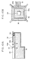
- the second conducting layer 418b in Fig. 12 is formed as a square ring in the region between the inner leads 32 and the frame lead 36.
- a conducting layer can be formed to surround the frame lead 336 in a way more simple than by forming a plurality of the second conducting layers at separate locations.
- Fig. 13 is a sectional view showing schematically essential portions of a semiconductor device 500 relating to a fifth embodiment of the invention.
- the semiconductor device 500 differs from the semiconductor device 100 shown in Fig. 2 in the form of the first conducting layer. Since the structure is the same as that of the semiconductor device 100 shown in Fig. 2 except for the first conducting layer, the description uses the same reference numerals.
- Fig. 2 illustrates that the first conducting layer 18a has a greater surface area than the area occupied by the semiconductor element 20.
- a first conducting layer 518a has a smaller surface area than the area occupied by the semiconductor element 20.
- the first conducting layer 18a is formed by for example silver plating, but this silver plating has poor bonding properties with the resin constituting the resin sealing portion 60.
- the insulating layer 16 is formed by oxidation, and has good bonding properties with the resin.
- the bonding contact of the resin sealing portion 60 with this portion is poor.
- the resin sealing portion 60 may peel away from the first conducting layer 18a, so that the reverse surface of the semiconductor element 20 comes away from the first conducting layer 18a, and the conductivity between these two will no longer be assured. This means that if the reverse surface of the semiconductor element 20 is used for example for a ground connection through the first conducting layer 18a, the electrical connection cannot be guaranteed.
- the first conducting layer 518a has a smaller surface area than the area occupied by the semiconductor element 20, and the first conducting layer 518a is arranged not to project outside the semiconductor element 20.
- first conducting layer 518a is formed in this way, it is not possible to connect grounding wires 44a, and it is preferable to form a conducting layer 518b (see Fig. 13) separate from the first conducting layer 518a.
- This conducting layer 518b is formed in a region disjoint from the reverse surface of the semiconductor element 20, so that it does not have any negative effect on the bonding properties of the semiconductor element 20 with the resin sealing portion 60.
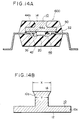
- Figs. 14A and 14B are sectional views showing schematically essential portions of a semiconductor device 600 relating to a sixth embodiment of the invention. Elements in this semiconductor device 600 which have substantially the same function as corresponding elements of the semiconductor device 100 of the first embodiment are given the same reference numerals, and detailed description of them is omitted here.
- the characteristic distinguished from the semiconductor device 100 is the shape of the element mounting portion 10.
- the small portion 10b has an undercut form, with the width X of the exposed surface 14 greater than the width Y below and parallel to the exposed surface 14. By means of this undercut form, the small portion 10b retains the resin sealing portion 60, and further increases the mechanical strength of the package.
- the distance from the exposed surface 14 to the large portion 10a is increased, and at least some protection against water ingress is obtained.
- a first resist film 82 is disposed to one surface of a metal sheet 80 of for example copper having the same thickness as the element mounting portion 10 to be formed.
- the first resist film 82 is disposed at predetermined intervals in portions corresponding to the exposed surface 14 of the element mounting portion 10.
- a second resist film 84 is formed on the underside of the metal sheet 80.
- the metal sheet 80 is immersion etched by an etching solution with for example ferric chloride as its principal constituent.
- the metal sheet 80 is etched to a depth corresponding to the thickness of the small portion 10b of the element mounting portion 10.
- the resist films 82 and 84 are removed, and then as shown in Fig. 15D, the metal sheet 80 is mechanically separated at positions delimiting the large portions 10a of the element mounting portions 10, using for ' example a press operation or machining operation, thus forming the element mounting portions 10.
- an oxide layer forms on the etched surface, and this not only acts as an insulating layer, but also provides a surface having good bonding properties with the resin forming the resin sealing portion 60.
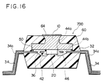
- a semiconductor device 700 relating to a seventh embodiment of the invention is described, with reference to Fig. 16.
- elements which have substantially the same function as corresponding elements of the sixth embodiment are given the same reference numerals, and detailed description of them is omitted here.
- the characteristic feature is that on the element mounting portion 10 is formed a conducting layer 64 of for example solder.
- This conducting layer 64 is for example formed while a solder plating layer 34a is formed on the surface of the outer leads 34 and in the same formation step as the solder plating layer 34a.
- a cooling fin is attached by adhesive, this is likely to be detached by the heat effects. If a cooling fin is attached by a clip mechanism, the contact area between the element mounting portion 10 and the cooling fin is small. As a result, forming the conducting layer 64 of solder and attaching the cooling fin is an effective method.
- solder is first also applied to the cooling fin, then the conducting layer 64 is heated to about 180 °C and the cooling fin is heated to about 300 °C. When the two are brought into contact, the solder melts at about 180 °C and the conducting layer 64 and the cooling fin are attached completely. Since only the cooling fin is heated to a high temperature and the semiconductor device 700 is kept at a relatively low temperature, the semiconductor element 20 can be protected from heat.
- a semiconductor device 800 relating to an eighth embodiment of the invention is now described, with reference to Fig. 17.
- Fig. 17 elements which are substantially the same as corresponding elements of the first embodiment are given the same reference numerals, and detailed description of them is omitted here. Additionally, description of grounding wires is omitted in Fig. 17.
- the characteristic feature is that the element mounting portion 10 is not exposed from the resin sealing portion 60, but is rather sealed within the resin sealing portion 60.
- the heat radiation efficiency is inferior to that of the exposed type.
- the semiconductor element and surrounding wiring is substantially totally sealed within the resin sealing portion 60, so that ingress of matter which might affect the semiconductor element or wiring can be more effectively prevented.
- the inner leads 32 are provided with support arms 30a formed integrally therewith, so that support of the inner leads 32 is assured, and deformation thereof is prevented. Since the support arms 30a are electrically conductive, it is necessary for at least an insulating layer 16 to be formed in the region of the element mounting portion 10 contacted by the ends of the support arms 30a.
- the support arms 30a are provided, but if for example the lead frame strength is increased, it may be possible to dispense with the support arms 30a.
- Fig. 18 illustrates the sequence for carrying out wire bonding of wires 40 on the electrode pads 22 of a semiconductor element 20.
- a plurality of electrode pads 22 are provided around the periphery of the surface of the semiconductor element 20, and wires 40 connecting to these electrode pads 22 are radially disposed from the center of the semiconductor element 20.
- the wires 40 connecting to the electrode pads 22 near the center of the side are disposed substantially at right angles to the side
- the wires 40 connecting to the electrode pads 22 near the corners are inclined at an oblique angle to the side.
- the closer to the corner the more oblique this inclination.
- the wires 40 near the corners are inclined at a large oblique angle to the side, and moving parallel to the orientation of the electrode pads toward the center, this oblique inclination becomes more perpendicular, and close to the center the wires are disposed substantially perpendicular to this orientation.
- the wire bonding proposed here is sequentially carried out starting near a corner and progressing toward the center.
- the wire bonding progresses from wires disposed at a large inclination to the orientation of the electrode pads 22 (the wires 40 near the corner) to wires 40 disposed at an angle close to perpendicular to the orientation of the electrode pads 22 (the wires 40 near the center), and in the direction in which the inclination becomes progressively more perpendicular.
- wires 40a, 40b, 40c and etc. are connected in sequence to the electrode pads 22a, 22b, 22c, and etc.
- the electrode pads 22 are connected in the sequence 22c, 22b and 22a from the center to the corner, by the wires 40c, 40b, and 40a.
- the wire 40c firstly when after connecting the wire 40c, the wire 40b is connected, the jig clamping the wire (shown as a broken circle in the figure) will contact the wire 40c.
- the wire 40a when after connecting the wire 40b, the wire 40a is connected, the jig clamping the wire will contact the wire 40b.
- Figs. 19A to 19D illustrate a preferred embodiment relating to resin sealing.
Landscapes
- Lead Frames For Integrated Circuits (AREA)
- Structures Or Materials For Encapsulating Or Coating Semiconductor Devices Or Solid State Devices (AREA)
- Wire Bonding (AREA)
- Cooling Or The Like Of Semiconductors Or Solid State Devices (AREA)
Applications Claiming Priority (6)
| Application Number | Priority Date | Filing Date | Title |
|---|---|---|---|
| JP183854/94 | 1994-07-13 | ||
| JP18385494 | 1994-07-13 | ||
| JP18385494 | 1994-07-13 | ||
| JP9812795 | 1995-03-30 | ||
| JP98127/95 | 1995-03-30 | ||
| JP09812795A JP3509274B2 (ja) | 1994-07-13 | 1995-03-30 | 樹脂封止型半導体装置およびその製造方法 |
Publications (3)
| Publication Number | Publication Date |
|---|---|
| EP0693779A2 EP0693779A2 (en) | 1996-01-24 |
| EP0693779A3 EP0693779A3 (en) | 1997-01-08 |
| EP0693779B1 true EP0693779B1 (en) | 2002-05-02 |
Family
ID=26439327
Family Applications (1)
| Application Number | Title | Priority Date | Filing Date |
|---|---|---|---|
| EP95109655A Expired - Lifetime EP0693779B1 (en) | 1994-07-13 | 1995-06-21 | Resin sealing type semiconductor device and method of making the same |
Country Status (7)
| Country | Link |
|---|---|
| US (1) | US5633529A (https=) |
| EP (1) | EP0693779B1 (https=) |
| JP (1) | JP3509274B2 (https=) |
| KR (1) | KR100386052B1 (https=) |
| DE (1) | DE69526543T2 (https=) |
| SG (1) | SG65533A1 (https=) |
| TW (1) | TW293940B (https=) |
Families Citing this family (25)
| Publication number | Priority date | Publication date | Assignee | Title |
|---|---|---|---|---|
| AU4697496A (en) * | 1995-01-24 | 1996-08-14 | Intel Corporation | High performance integrated circuit package |
| JP3542677B2 (ja) * | 1995-02-27 | 2004-07-14 | セイコーエプソン株式会社 | 樹脂封止型半導体装置およびその製造方法 |
| JP3309686B2 (ja) * | 1995-03-17 | 2002-07-29 | セイコーエプソン株式会社 | 樹脂封止型半導体装置及びその製造方法 |
| JPH0964244A (ja) * | 1995-08-17 | 1997-03-07 | Hitachi Ltd | 半導体装置およびその製造方法 |
| US5757070A (en) * | 1995-10-24 | 1998-05-26 | Altera Corporation | Integrated circuit package |
| EP0848423B1 (en) * | 1996-07-03 | 2006-03-01 | Seiko Epson Corporation | Resin-encapsulated semiconductor device and method of manufacturing the same |
| JPH11274196A (ja) * | 1998-03-26 | 1999-10-08 | Seiko Epson Corp | 半導体装置の製造方法およびモールドシステム並びに半導体装置 |
| US6977214B2 (en) * | 1998-12-11 | 2005-12-20 | Micron Technology, Inc. | Die paddle clamping method for wire bond enhancement |
| US6455354B1 (en) | 1998-12-30 | 2002-09-24 | Micron Technology, Inc. | Method of fabricating tape attachment chip-on-board assemblies |
| US6212077B1 (en) | 1999-01-25 | 2001-04-03 | International Business Machines Corporation | Built-in inspection template for a printed circuit |
| WO2000074131A1 (en) * | 1999-05-31 | 2000-12-07 | Infineon Technologies A.G. | A method of assembling a semiconductor device package |
| JP2000349221A (ja) | 1999-06-02 | 2000-12-15 | Sharp Corp | リードフレームおよびそれを用いた半導体デバイス |
| MY133357A (en) * | 1999-06-30 | 2007-11-30 | Hitachi Ltd | A semiconductor device and a method of manufacturing the same |
| JP2001230360A (ja) * | 2000-02-18 | 2001-08-24 | Hitachi Ltd | 半導体集積回路装置およびその製造方法 |
| US6688353B1 (en) | 2000-03-31 | 2004-02-10 | Bridgestone/Firestone North American Tire, Llc | Attachment patch for mounting an electronic monitoring device to the inside of a pneumatic tire |
| CN1265451C (zh) * | 2000-09-06 | 2006-07-19 | 三洋电机株式会社 | 半导体装置及其制造方法 |
| US6838751B2 (en) * | 2002-03-06 | 2005-01-04 | Freescale Semiconductor Inc. | Multi-row leadframe |
| US7309447B2 (en) * | 2003-02-03 | 2007-12-18 | Tessera, Inc. | Method for making a microelectronic package using pre-patterned, reusable mold and method for making the mold |
| US20050285281A1 (en) * | 2004-06-29 | 2005-12-29 | Simmons Asher L | Pad-limited integrated circuit |
| US20070200225A1 (en) * | 2006-02-28 | 2007-08-30 | Ruzaini Ibrahim | Heat sink for semiconductor package |
| JP5132070B2 (ja) * | 2006-03-31 | 2013-01-30 | オンセミコンダクター・トレーディング・リミテッド | 回路装置およびその製造方法 |
| JP2008300492A (ja) * | 2007-05-30 | 2008-12-11 | Rohm Co Ltd | 半導体装置 |
| US8643172B2 (en) | 2007-06-08 | 2014-02-04 | Freescale Semiconductor, Inc. | Heat spreader for center gate molding |
| US20110012257A1 (en) * | 2009-07-14 | 2011-01-20 | Freescale Semiconductor, Inc | Heat spreader for semiconductor package |
| JP6111973B2 (ja) * | 2013-10-15 | 2017-04-12 | 株式会社デンソー | 半導体装置 |
Family Cites Families (54)
| Publication number | Priority date | Publication date | Assignee | Title |
|---|---|---|---|---|
| NL121811C (https=) * | 1961-06-26 | |||
| US3290564A (en) * | 1963-02-26 | 1966-12-06 | Texas Instruments Inc | Semiconductor device |
| US3965277A (en) * | 1972-05-09 | 1976-06-22 | Massachusetts Institute Of Technology | Photoformed plated interconnection of embedded integrated circuit chips |
| JPS52124865A (en) * | 1976-04-13 | 1977-10-20 | Sharp Corp | Semiconductor device |
| JPS54124678A (en) * | 1978-03-20 | 1979-09-27 | Nec Corp | Lead frame |
| JPS56122134A (en) * | 1980-02-29 | 1981-09-25 | Toshiba Corp | Resin-sealed type semiconductor device |
| JPS5812341A (ja) * | 1981-07-16 | 1983-01-24 | Toshiba Corp | 半導体装置 |
| JPS59207645A (ja) * | 1983-05-11 | 1984-11-24 | Toshiba Corp | 半導体装置およびリ−ドフレ−ム |
| EP0164794B1 (en) * | 1984-06-14 | 1990-07-25 | Advanced Micro Devices, Inc. | Multi-layer heat sinking integrated circuit package |
| JPS61166051A (ja) * | 1985-01-17 | 1986-07-26 | Matsushita Electronics Corp | 樹脂封止型半導体装置 |
| JPS6297358A (ja) * | 1985-10-23 | 1987-05-06 | Mitsubishi Electric Corp | 樹脂封止形半導体集積回路装置 |
| US4684975A (en) * | 1985-12-16 | 1987-08-04 | National Semiconductor Corporation | Molded semiconductor package having improved heat dissipation |
| JPS63179557A (ja) * | 1987-01-20 | 1988-07-23 | Nec Corp | 半導体装置用リ−ドフレ−ム |
| JPS63200554A (ja) * | 1987-02-16 | 1988-08-18 | Nec Corp | 半導体装置 |
| JPS63240053A (ja) * | 1987-03-27 | 1988-10-05 | Mitsubishi Electric Corp | 半導体装置 |
| US4942497A (en) * | 1987-07-24 | 1990-07-17 | Nec Corporation | Cooling structure for heat generating electronic components mounted on a substrate |
| JP2532041B2 (ja) * | 1987-10-05 | 1996-09-11 | 新光電気工業株式会社 | 半導体装置用リ―ドフレ―ム |
| US5050040A (en) * | 1988-10-21 | 1991-09-17 | Texas Instruments Incorporated | Composite material, a heat-dissipating member using the material in a circuit system, the circuit system |
| US5157478A (en) * | 1989-04-19 | 1992-10-20 | Mitsubishi Denki Kabushiki Kaisha | Tape automated bonding packaged semiconductor device incorporating a heat sink |
| JPH02307251A (ja) * | 1989-05-22 | 1990-12-20 | Nec Corp | 樹脂封止型半導体装置 |
| US5278101A (en) * | 1989-06-28 | 1994-01-11 | Kabushiki Kaisha Toshiba | Semiconductor device and method for manufacturing the same |
| US5208188A (en) * | 1989-10-02 | 1993-05-04 | Advanced Micro Devices, Inc. | Process for making a multilayer lead frame assembly for an integrated circuit structure and multilayer integrated circuit die package formed by such process |
| JPH0719876B2 (ja) * | 1989-12-04 | 1995-03-06 | 株式会社東芝 | 半導体装置 |
| JP2517691B2 (ja) * | 1990-01-29 | 1996-07-24 | 三菱電機株式会社 | 半導体装置及びその製造方法 |
| JPH0410558A (ja) * | 1990-04-27 | 1992-01-14 | Hitachi Ltd | 放熱体付き半導体装置 |
| JPH0411758A (ja) * | 1990-04-28 | 1992-01-16 | Mitsubishi Electric Corp | 半導体装置 |
| JPH0427145A (ja) * | 1990-05-22 | 1992-01-30 | Seiko Epson Corp | 半導体装置 |
| US5227662A (en) * | 1990-05-24 | 1993-07-13 | Nippon Steel Corporation | Composite lead frame and semiconductor device using the same |
| US5202288A (en) * | 1990-06-01 | 1993-04-13 | Robert Bosch Gmbh | Method of manufacturing an electronic circuit component incorporating a heat sink |
| DE4017697C2 (de) * | 1990-06-01 | 2003-12-11 | Bosch Gmbh Robert | Elektronisches Bauelement, Verfahren zu dessen Herstellung und Verwendung |
| JP2983620B2 (ja) * | 1990-07-20 | 1999-11-29 | 株式会社日立製作所 | 半導体装置及びその製造方法 |
| JP3047986B2 (ja) * | 1990-07-25 | 2000-06-05 | 株式会社日立製作所 | 半導体装置 |
| JP2725448B2 (ja) * | 1990-08-01 | 1998-03-11 | 三菱電機株式会社 | 半導体装置 |
| US5105259A (en) * | 1990-09-28 | 1992-04-14 | Motorola, Inc. | Thermally enhanced semiconductor device utilizing a vacuum to ultimately enhance thermal dissipation |
| JPH04158556A (ja) * | 1990-10-22 | 1992-06-01 | Toshiba Corp | 樹脂封止型半導体装置 |
| JPH04162556A (ja) * | 1990-10-25 | 1992-06-08 | Mitsubishi Electric Corp | リードフレーム及びその製造方法 |
| JP2841854B2 (ja) * | 1990-11-29 | 1998-12-24 | セイコーエプソン株式会社 | 半導体装置 |
| JPH04316357A (ja) * | 1991-04-15 | 1992-11-06 | Sony Corp | 樹脂封止型半導体装置 |
| US5172213A (en) * | 1991-05-23 | 1992-12-15 | At&T Bell Laboratories | Molded circuit package having heat dissipating post |
| US5200809A (en) * | 1991-09-27 | 1993-04-06 | Vlsi Technology, Inc. | Exposed die-attach heatsink package |
| JP2602380B2 (ja) * | 1991-10-23 | 1997-04-23 | 富士通株式会社 | 半導体装置及びその製造方法 |
| JPH05190721A (ja) * | 1992-01-08 | 1993-07-30 | Fujitsu Ltd | 半導体装置及びその製造方法 |
| JPH05211262A (ja) * | 1992-01-08 | 1993-08-20 | Nec Corp | 樹脂封止型半導体装置 |
| US5328870A (en) * | 1992-01-17 | 1994-07-12 | Amkor Electronics, Inc. | Method for forming plastic molded package with heat sink for integrated circuit devices |
| US5262927A (en) * | 1992-02-07 | 1993-11-16 | Lsi Logic Corporation | Partially-molded, PCB chip carrier package |
| JPH06120374A (ja) * | 1992-03-31 | 1994-04-28 | Amkor Electron Inc | 半導体パッケージ構造、半導体パッケージ方法及び半導体パッケージ用放熱板 |
| JPH0653346A (ja) * | 1992-06-02 | 1994-02-25 | Fujitsu Ltd | 半導体装置 |
| JP3572628B2 (ja) * | 1992-06-03 | 2004-10-06 | セイコーエプソン株式会社 | 半導体装置及びその製造方法 |
| JP3322429B2 (ja) * | 1992-06-04 | 2002-09-09 | 新光電気工業株式会社 | 半導体装置 |
| US5367196A (en) * | 1992-09-17 | 1994-11-22 | Olin Corporation | Molded plastic semiconductor package including an aluminum alloy heat spreader |
| JP2848151B2 (ja) | 1992-08-20 | 1999-01-20 | トヨタ自動車株式会社 | ディファレンシャル装置のバックラッシシム選択方法 |
| JPH0697326A (ja) * | 1992-09-14 | 1994-04-08 | Apic Yamada Kk | 半導体装置およびその放熱部材 |
| JPH06295962A (ja) * | 1992-10-20 | 1994-10-21 | Ibiden Co Ltd | 電子部品搭載用基板およびその製造方法並びに電子部品搭載装置 |
| JPH06151485A (ja) * | 1992-11-12 | 1994-05-31 | Sumitomo Electric Ind Ltd | 半導体装置用パッケージ |
-
1995
- 1995-03-30 JP JP09812795A patent/JP3509274B2/ja not_active Expired - Fee Related
- 1995-06-05 US US08/461,442 patent/US5633529A/en not_active Expired - Lifetime
- 1995-06-09 TW TW084105885A patent/TW293940B/zh not_active IP Right Cessation
- 1995-06-21 DE DE69526543T patent/DE69526543T2/de not_active Expired - Fee Related
- 1995-06-21 EP EP95109655A patent/EP0693779B1/en not_active Expired - Lifetime
- 1995-07-06 SG SG1995000813A patent/SG65533A1/en unknown
- 1995-07-12 KR KR1019950020417A patent/KR100386052B1/ko not_active Expired - Fee Related
Also Published As
| Publication number | Publication date |
|---|---|
| US5633529A (en) | 1997-05-27 |
| JP3509274B2 (ja) | 2004-03-22 |
| TW293940B (https=) | 1996-12-21 |
| DE69526543D1 (de) | 2002-06-06 |
| JPH0883876A (ja) | 1996-03-26 |
| HK1013888A1 (en) | 1999-09-10 |
| EP0693779A3 (en) | 1997-01-08 |
| KR960005972A (ko) | 1996-02-23 |
| KR100386052B1 (ko) | 2003-08-09 |
| EP0693779A2 (en) | 1996-01-24 |
| DE69526543T2 (de) | 2002-10-31 |
| SG65533A1 (en) | 1999-06-22 |
Similar Documents
| Publication | Publication Date | Title |
|---|---|---|
| US6133623A (en) | Resin sealing type semiconductor device that includes a plurality of leads and method of making the same | |
| EP0693779B1 (en) | Resin sealing type semiconductor device and method of making the same | |
| US5874784A (en) | Semiconductor device having external connection terminals provided on an interconnection plate and fabrication process therefor | |
| KR100294719B1 (ko) | 수지밀봉형 반도체장치 및 그 제조방법, 리드프레임 | |
| US5653891A (en) | Method of producing a semiconductor device with a heat sink | |
| US7911054B2 (en) | Semiconductor device | |
| KR100229858B1 (ko) | 반도체 장치 | |
| JPWO1998001907A1 (ja) | 樹脂封止型半導体装置およびその製造方法 | |
| JP3238004B2 (ja) | 半導体装置の製造方法 | |
| EP0732744B1 (en) | Resin sealing type semiconductor device and method of making the same | |
| KR19990072580A (ko) | 반도체장치,반도체장치용기판및이들의제조방법및전자기기 | |
| KR100414450B1 (ko) | 수지봉지형반도체장치및그제조방법 | |
| HK1013888B (en) | Resin sealing type semiconductor device and method of making the same | |
| JPH11297752A (ja) | 半導体チップの実装構造、およびこの実装構造を有する半導体装置 | |
| JP3827978B2 (ja) | 半導体装置の製造方法 | |
| JP3855941B2 (ja) | 凸型ヒートシンク付き半導体装置の製造方法 | |
| JPH09199631A (ja) | 半導体装置の構造と製造方法 | |
| JP3211116B2 (ja) | 電子部品及びそのモジュール構造 | |
| HK1013734B (en) | Resin sealing type semiconductor device and method of making the same | |
| JPH04196349A (ja) | 樹脂封止型半導体装置 | |
| JPS62224033A (ja) | テ−プキヤリア装置 | |
| JP2000243789A (ja) | Bga用テープキャリア及びこれを用いた半導体装置 | |
| JPH10270595A (ja) | 半導体装置及びその製造方法 | |
| HK1013887A (en) | Resin sealing type semiconductor device and method of making the same | |
| JP2000243790A (ja) | Tabテープ及びこれを用いた半導体装置 |
Legal Events
| Date | Code | Title | Description |
|---|---|---|---|
| PUAI | Public reference made under article 153(3) epc to a published international application that has entered the european phase |
Free format text: ORIGINAL CODE: 0009012 |
|
| AK | Designated contracting states |
Kind code of ref document: A2 Designated state(s): DE FR GB |
|
| PUAL | Search report despatched |
Free format text: ORIGINAL CODE: 0009013 |
|
| RHK1 | Main classification (correction) |
Ipc: H01L 23/495 |
|
| AK | Designated contracting states |
Kind code of ref document: A3 Designated state(s): DE FR GB |
|
| 17P | Request for examination filed |
Effective date: 19970410 |
|
| 17Q | First examination report despatched |
Effective date: 19990311 |
|
| GRAG | Despatch of communication of intention to grant |
Free format text: ORIGINAL CODE: EPIDOS AGRA |
|
| GRAG | Despatch of communication of intention to grant |
Free format text: ORIGINAL CODE: EPIDOS AGRA |
|
| GRAH | Despatch of communication of intention to grant a patent |
Free format text: ORIGINAL CODE: EPIDOS IGRA |
|
| GRAH | Despatch of communication of intention to grant a patent |
Free format text: ORIGINAL CODE: EPIDOS IGRA |
|
| REG | Reference to a national code |
Ref country code: GB Ref legal event code: IF02 |
|
| GRAA | (expected) grant |
Free format text: ORIGINAL CODE: 0009210 |
|
| AK | Designated contracting states |
Kind code of ref document: B1 Designated state(s): DE FR GB |
|
| REG | Reference to a national code |
Ref country code: GB Ref legal event code: FG4D |
|
| REF | Corresponds to: |
Ref document number: 69526543 Country of ref document: DE Date of ref document: 20020606 |
|
| ET | Fr: translation filed | ||
| PLBE | No opposition filed within time limit |
Free format text: ORIGINAL CODE: 0009261 |
|
| STAA | Information on the status of an ep patent application or granted ep patent |
Free format text: STATUS: NO OPPOSITION FILED WITHIN TIME LIMIT |
|
| 26N | No opposition filed |
Effective date: 20030204 |
|
| PGFP | Annual fee paid to national office [announced via postgrant information from national office to epo] |
Ref country code: GB Payment date: 20090617 Year of fee payment: 15 Ref country code: DE Payment date: 20090619 Year of fee payment: 15 |
|
| GBPC | Gb: european patent ceased through non-payment of renewal fee |
Effective date: 20100621 |
|
| REG | Reference to a national code |
Ref country code: FR Ref legal event code: ST Effective date: 20110228 |
|
| PG25 | Lapsed in a contracting state [announced via postgrant information from national office to epo] |
Ref country code: DE Free format text: LAPSE BECAUSE OF NON-PAYMENT OF DUE FEES Effective date: 20110101 |
|
| PG25 | Lapsed in a contracting state [announced via postgrant information from national office to epo] |
Ref country code: FR Free format text: LAPSE BECAUSE OF NON-PAYMENT OF DUE FEES Effective date: 20100630 |
|
| PG25 | Lapsed in a contracting state [announced via postgrant information from national office to epo] |
Ref country code: GB Free format text: LAPSE BECAUSE OF NON-PAYMENT OF DUE FEES Effective date: 20100621 |
|
| PGFP | Annual fee paid to national office [announced via postgrant information from national office to epo] |
Ref country code: FR Payment date: 20090611 Year of fee payment: 15 |