EP0164794B1 - Multi-layer heat sinking integrated circuit package - Google Patents
Multi-layer heat sinking integrated circuit package Download PDFInfo
- Publication number
- EP0164794B1 EP0164794B1 EP85200826A EP85200826A EP0164794B1 EP 0164794 B1 EP0164794 B1 EP 0164794B1 EP 85200826 A EP85200826 A EP 85200826A EP 85200826 A EP85200826 A EP 85200826A EP 0164794 B1 EP0164794 B1 EP 0164794B1
- Authority
- EP
- European Patent Office
- Prior art keywords
- die
- package
- base
- lead
- preform
- Prior art date
- Legal status (The legal status is an assumption and is not a legal conclusion. Google has not performed a legal analysis and makes no representation as to the accuracy of the status listed.)
- Expired - Lifetime
Links
Images
Classifications
-
- H—ELECTRICITY
- H01—ELECTRIC ELEMENTS
- H01L—SEMICONDUCTOR DEVICES NOT COVERED BY CLASS H10
- H01L23/00—Details of semiconductor or other solid state devices
- H01L23/02—Containers; Seals
- H01L23/04—Containers; Seals characterised by the shape of the container or parts, e.g. caps, walls
- H01L23/043—Containers; Seals characterised by the shape of the container or parts, e.g. caps, walls the container being a hollow construction and having a conductive base as a mounting as well as a lead for the semiconductor body
- H01L23/047—Containers; Seals characterised by the shape of the container or parts, e.g. caps, walls the container being a hollow construction and having a conductive base as a mounting as well as a lead for the semiconductor body the other leads being parallel to the base
-
- H—ELECTRICITY
- H01—ELECTRIC ELEMENTS
- H01L—SEMICONDUCTOR DEVICES NOT COVERED BY CLASS H10
- H01L23/00—Details of semiconductor or other solid state devices
- H01L23/34—Arrangements for cooling, heating, ventilating or temperature compensation ; Temperature sensing arrangements
- H01L23/36—Selection of materials, or shaping, to facilitate cooling or heating, e.g. heatsinks
- H01L23/373—Cooling facilitated by selection of materials for the device or materials for thermal expansion adaptation, e.g. carbon
- H01L23/3735—Laminates or multilayers, e.g. direct bond copper ceramic substrates
-
- H—ELECTRICITY
- H01—ELECTRIC ELEMENTS
- H01L—SEMICONDUCTOR DEVICES NOT COVERED BY CLASS H10
- H01L23/00—Details of semiconductor or other solid state devices
- H01L23/48—Arrangements for conducting electric current to or from the solid state body in operation, e.g. leads, terminal arrangements ; Selection of materials therefor
- H01L23/482—Arrangements for conducting electric current to or from the solid state body in operation, e.g. leads, terminal arrangements ; Selection of materials therefor consisting of lead-in layers inseparably applied to the semiconductor body
- H01L23/4827—Materials
- H01L23/4828—Conductive organic material or pastes, e.g. conductive adhesives, inks
-
- H—ELECTRICITY
- H01—ELECTRIC ELEMENTS
- H01L—SEMICONDUCTOR DEVICES NOT COVERED BY CLASS H10
- H01L2224/00—Indexing scheme for arrangements for connecting or disconnecting semiconductor or solid-state bodies and methods related thereto as covered by H01L24/00
- H01L2224/01—Means for bonding being attached to, or being formed on, the surface to be connected, e.g. chip-to-package, die-attach, "first-level" interconnects; Manufacturing methods related thereto
- H01L2224/42—Wire connectors; Manufacturing methods related thereto
- H01L2224/44—Structure, shape, material or disposition of the wire connectors prior to the connecting process
- H01L2224/45—Structure, shape, material or disposition of the wire connectors prior to the connecting process of an individual wire connector
- H01L2224/45001—Core members of the connector
- H01L2224/4501—Shape
- H01L2224/45012—Cross-sectional shape
- H01L2224/45015—Cross-sectional shape being circular
-
- H—ELECTRICITY
- H01—ELECTRIC ELEMENTS
- H01L—SEMICONDUCTOR DEVICES NOT COVERED BY CLASS H10
- H01L2224/00—Indexing scheme for arrangements for connecting or disconnecting semiconductor or solid-state bodies and methods related thereto as covered by H01L24/00
- H01L2224/01—Means for bonding being attached to, or being formed on, the surface to be connected, e.g. chip-to-package, die-attach, "first-level" interconnects; Manufacturing methods related thereto
- H01L2224/42—Wire connectors; Manufacturing methods related thereto
- H01L2224/44—Structure, shape, material or disposition of the wire connectors prior to the connecting process
- H01L2224/45—Structure, shape, material or disposition of the wire connectors prior to the connecting process of an individual wire connector
- H01L2224/45001—Core members of the connector
- H01L2224/45099—Material
- H01L2224/451—Material with a principal constituent of the material being a metal or a metalloid, e.g. boron (B), silicon (Si), germanium (Ge), arsenic (As), antimony (Sb), tellurium (Te) and polonium (Po), and alloys thereof
- H01L2224/45138—Material with a principal constituent of the material being a metal or a metalloid, e.g. boron (B), silicon (Si), germanium (Ge), arsenic (As), antimony (Sb), tellurium (Te) and polonium (Po), and alloys thereof the principal constituent melting at a temperature of greater than or equal to 950°C and less than 1550°C
- H01L2224/45144—Gold (Au) as principal constituent
-
- H—ELECTRICITY
- H01—ELECTRIC ELEMENTS
- H01L—SEMICONDUCTOR DEVICES NOT COVERED BY CLASS H10
- H01L2224/00—Indexing scheme for arrangements for connecting or disconnecting semiconductor or solid-state bodies and methods related thereto as covered by H01L24/00
- H01L2224/01—Means for bonding being attached to, or being formed on, the surface to be connected, e.g. chip-to-package, die-attach, "first-level" interconnects; Manufacturing methods related thereto
- H01L2224/42—Wire connectors; Manufacturing methods related thereto
- H01L2224/47—Structure, shape, material or disposition of the wire connectors after the connecting process
- H01L2224/48—Structure, shape, material or disposition of the wire connectors after the connecting process of an individual wire connector
- H01L2224/4805—Shape
- H01L2224/4809—Loop shape
- H01L2224/48091—Arched
-
- H—ELECTRICITY
- H01—ELECTRIC ELEMENTS
- H01L—SEMICONDUCTOR DEVICES NOT COVERED BY CLASS H10
- H01L2224/00—Indexing scheme for arrangements for connecting or disconnecting semiconductor or solid-state bodies and methods related thereto as covered by H01L24/00
- H01L2224/01—Means for bonding being attached to, or being formed on, the surface to be connected, e.g. chip-to-package, die-attach, "first-level" interconnects; Manufacturing methods related thereto
- H01L2224/42—Wire connectors; Manufacturing methods related thereto
- H01L2224/47—Structure, shape, material or disposition of the wire connectors after the connecting process
- H01L2224/48—Structure, shape, material or disposition of the wire connectors after the connecting process of an individual wire connector
- H01L2224/481—Disposition
- H01L2224/48151—Connecting between a semiconductor or solid-state body and an item not being a semiconductor or solid-state body, e.g. chip-to-substrate, chip-to-passive
- H01L2224/48221—Connecting between a semiconductor or solid-state body and an item not being a semiconductor or solid-state body, e.g. chip-to-substrate, chip-to-passive the body and the item being stacked
- H01L2224/48245—Connecting between a semiconductor or solid-state body and an item not being a semiconductor or solid-state body, e.g. chip-to-substrate, chip-to-passive the body and the item being stacked the item being metallic
- H01L2224/48247—Connecting between a semiconductor or solid-state body and an item not being a semiconductor or solid-state body, e.g. chip-to-substrate, chip-to-passive the body and the item being stacked the item being metallic connecting the wire to a bond pad of the item
-
- H—ELECTRICITY
- H01—ELECTRIC ELEMENTS
- H01L—SEMICONDUCTOR DEVICES NOT COVERED BY CLASS H10
- H01L2224/00—Indexing scheme for arrangements for connecting or disconnecting semiconductor or solid-state bodies and methods related thereto as covered by H01L24/00
- H01L2224/73—Means for bonding being of different types provided for in two or more of groups H01L2224/10, H01L2224/18, H01L2224/26, H01L2224/34, H01L2224/42, H01L2224/50, H01L2224/63, H01L2224/71
- H01L2224/732—Location after the connecting process
- H01L2224/73251—Location after the connecting process on different surfaces
- H01L2224/73265—Layer and wire connectors
-
- H—ELECTRICITY
- H01—ELECTRIC ELEMENTS
- H01L—SEMICONDUCTOR DEVICES NOT COVERED BY CLASS H10
- H01L24/00—Arrangements for connecting or disconnecting semiconductor or solid-state bodies; Methods or apparatus related thereto
- H01L24/01—Means for bonding being attached to, or being formed on, the surface to be connected, e.g. chip-to-package, die-attach, "first-level" interconnects; Manufacturing methods related thereto
- H01L24/42—Wire connectors; Manufacturing methods related thereto
- H01L24/44—Structure, shape, material or disposition of the wire connectors prior to the connecting process
- H01L24/45—Structure, shape, material or disposition of the wire connectors prior to the connecting process of an individual wire connector
-
- H—ELECTRICITY
- H01—ELECTRIC ELEMENTS
- H01L—SEMICONDUCTOR DEVICES NOT COVERED BY CLASS H10
- H01L24/00—Arrangements for connecting or disconnecting semiconductor or solid-state bodies; Methods or apparatus related thereto
- H01L24/01—Means for bonding being attached to, or being formed on, the surface to be connected, e.g. chip-to-package, die-attach, "first-level" interconnects; Manufacturing methods related thereto
- H01L24/42—Wire connectors; Manufacturing methods related thereto
- H01L24/47—Structure, shape, material or disposition of the wire connectors after the connecting process
- H01L24/48—Structure, shape, material or disposition of the wire connectors after the connecting process of an individual wire connector
-
- H—ELECTRICITY
- H01—ELECTRIC ELEMENTS
- H01L—SEMICONDUCTOR DEVICES NOT COVERED BY CLASS H10
- H01L2924/00—Indexing scheme for arrangements or methods for connecting or disconnecting semiconductor or solid-state bodies as covered by H01L24/00
- H01L2924/0001—Technical content checked by a classifier
- H01L2924/00014—Technical content checked by a classifier the subject-matter covered by the group, the symbol of which is combined with the symbol of this group, being disclosed without further technical details
-
- H—ELECTRICITY
- H01—ELECTRIC ELEMENTS
- H01L—SEMICONDUCTOR DEVICES NOT COVERED BY CLASS H10
- H01L2924/00—Indexing scheme for arrangements or methods for connecting or disconnecting semiconductor or solid-state bodies as covered by H01L24/00
- H01L2924/01—Chemical elements
- H01L2924/0102—Calcium [Ca]
-
- H—ELECTRICITY
- H01—ELECTRIC ELEMENTS
- H01L—SEMICONDUCTOR DEVICES NOT COVERED BY CLASS H10
- H01L2924/00—Indexing scheme for arrangements or methods for connecting or disconnecting semiconductor or solid-state bodies as covered by H01L24/00
- H01L2924/01—Chemical elements
- H01L2924/01046—Palladium [Pd]
-
- H—ELECTRICITY
- H01—ELECTRIC ELEMENTS
- H01L—SEMICONDUCTOR DEVICES NOT COVERED BY CLASS H10
- H01L2924/00—Indexing scheme for arrangements or methods for connecting or disconnecting semiconductor or solid-state bodies as covered by H01L24/00
- H01L2924/01—Chemical elements
- H01L2924/01079—Gold [Au]
-
- H—ELECTRICITY
- H01—ELECTRIC ELEMENTS
- H01L—SEMICONDUCTOR DEVICES NOT COVERED BY CLASS H10
- H01L2924/00—Indexing scheme for arrangements or methods for connecting or disconnecting semiconductor or solid-state bodies as covered by H01L24/00
- H01L2924/10—Details of semiconductor or other solid state devices to be connected
- H01L2924/11—Device type
- H01L2924/14—Integrated circuits
-
- H—ELECTRICITY
- H01—ELECTRIC ELEMENTS
- H01L—SEMICONDUCTOR DEVICES NOT COVERED BY CLASS H10
- H01L2924/00—Indexing scheme for arrangements or methods for connecting or disconnecting semiconductor or solid-state bodies as covered by H01L24/00
- H01L2924/15—Details of package parts other than the semiconductor or other solid state devices to be connected
- H01L2924/151—Die mounting substrate
- H01L2924/1515—Shape
- H01L2924/15153—Shape the die mounting substrate comprising a recess for hosting the device
-
- H—ELECTRICITY
- H01—ELECTRIC ELEMENTS
- H01L—SEMICONDUCTOR DEVICES NOT COVERED BY CLASS H10
- H01L2924/00—Indexing scheme for arrangements or methods for connecting or disconnecting semiconductor or solid-state bodies as covered by H01L24/00
- H01L2924/15—Details of package parts other than the semiconductor or other solid state devices to be connected
- H01L2924/151—Die mounting substrate
- H01L2924/1517—Multilayer substrate
-
- H—ELECTRICITY
- H01—ELECTRIC ELEMENTS
- H01L—SEMICONDUCTOR DEVICES NOT COVERED BY CLASS H10
- H01L2924/00—Indexing scheme for arrangements or methods for connecting or disconnecting semiconductor or solid-state bodies as covered by H01L24/00
- H01L2924/15—Details of package parts other than the semiconductor or other solid state devices to be connected
- H01L2924/151—Die mounting substrate
- H01L2924/156—Material
- H01L2924/157—Material with a principal constituent of the material being a metal or a metalloid, e.g. boron [B], silicon [Si], germanium [Ge], arsenic [As], antimony [Sb], tellurium [Te] and polonium [Po], and alloys thereof
- H01L2924/15738—Material with a principal constituent of the material being a metal or a metalloid, e.g. boron [B], silicon [Si], germanium [Ge], arsenic [As], antimony [Sb], tellurium [Te] and polonium [Po], and alloys thereof the principal constituent melting at a temperature of greater than or equal to 950 C and less than 1550 C
- H01L2924/15747—Copper [Cu] as principal constituent
-
- H—ELECTRICITY
- H01—ELECTRIC ELEMENTS
- H01L—SEMICONDUCTOR DEVICES NOT COVERED BY CLASS H10
- H01L2924/00—Indexing scheme for arrangements or methods for connecting or disconnecting semiconductor or solid-state bodies as covered by H01L24/00
- H01L2924/15—Details of package parts other than the semiconductor or other solid state devices to be connected
- H01L2924/161—Cap
- H01L2924/1615—Shape
- H01L2924/16152—Cap comprising a cavity for hosting the device, e.g. U-shaped cap
-
- H—ELECTRICITY
- H01—ELECTRIC ELEMENTS
- H01L—SEMICONDUCTOR DEVICES NOT COVERED BY CLASS H10
- H01L2924/00—Indexing scheme for arrangements or methods for connecting or disconnecting semiconductor or solid-state bodies as covered by H01L24/00
- H01L2924/15—Details of package parts other than the semiconductor or other solid state devices to be connected
- H01L2924/181—Encapsulation
-
- H—ELECTRICITY
- H01—ELECTRIC ELEMENTS
- H01L—SEMICONDUCTOR DEVICES NOT COVERED BY CLASS H10
- H01L2924/00—Indexing scheme for arrangements or methods for connecting or disconnecting semiconductor or solid-state bodies as covered by H01L24/00
- H01L2924/30—Technical effects
- H01L2924/301—Electrical effects
- H01L2924/3011—Impedance
Definitions
- the present invention relates to an integrated circuit (IC) package, more particularly to a simplified multi-layer package having heat-sink means to quickly remove heat generated within the package by operation of the integrated circuit.
- IC integrated circuit
- the prior art material to this invention is typified by U.S. Patent 4,338,621 (Braun) wherein a hermetically sealed IC package is back bonded in a recessed lower conductive ceramic member (with cooling enhanced by fins) and an upper conductive ceramic member mounting input/output pins is sealed thereto. Interior interconnections are connected by wire bonds to the die and through metallized vias to the input/output pins. A metal seal ring is provided between the two ceramic members.
- the Braun patent is a special custom design involving a large number of manufacturing steps.
- insulative cover means cooperating with a further preform for covering said die attach surface and die.
- the package of the present invention as claimed provides a simplified heat-sink package which essentially keeps the exterior configuration of a standard ceramic or plastic dual-in-line (DIP) or castellated package for example, for VLSI or gate array applications.
- DIP dual-in-line
- the heat rejection characteristics of the package are vastly improved while employing standard lead-frames and without the addition of customizing features.
- This invention provides a semiconductor IC package type which allows the mounting of the die directly to a highly thermally conductive substrate which is exposed to the external ambient.
- the package design allows for various configurations, such as a dual-in-line package, flat pack, i.e., flat leads extending from the package, quad (displaced bend leads), or the like.
- Construction allows for the use of conventional technology to provide a lead frame, base, and cap. This includes the use of a metallic (or other highly conductive) base plate corresponding to the base of a ceramic dual-in-line package device.
- a lead frame similar to that used for flat packs is bonded to the base by means of a glass epoxy preform or pre-preg laminate (normally of electrically insulating material).
- the IC die is then mounted to the base by thermally conductive means, either epoxy or filed glass die attach paste, and interconnections made between the bond pads of the die and posts of the lead frame by wire bond or other means.
- thermally conductive means either epoxy or filed glass die attach paste
- interconnections made between the bond pads of the die and posts of the lead frame by wire bond or other means.
- a cap of electrically insulating or conductive material is then bonded over the package in a manner not to interfere with the electrical operation of the device. After this operation, the package is sufficiently structurally sound to allow for any required lead forming operations.
- the package of the invention provides for excellent dissipation of heat generated by the internal IC in a very simplified manner without changing the standard exterior configuration of a standard DIP enclosure, thus continuing to permit close mounting and standard orientation of DIP packages on circuit boards using standard manufacturing and assembly equipment.
- the heat-sink package 10 which confroms in exterior configuration to a standard DIP package but having vastly improved heat rejection capabilities is seen in Figure 1.
- a rectangular base 11 of thermally conductive material such as copper or aluminum or alloys thereof or beryllia (BeO) having a coefficient of thermal conductivity of at least 1.0467 joules per sec. per cm per °C (0.25 cal/°C s cm), has an exterior dimension substantially the same as a standard DIP package.
- Standard packages vary in size dependent on the number of input/output terminals in flat contacts extending therefrom for example 16, 20 and 24 terminals.
- each number of terminals the dimensions can slightly vary generally, for example, a 20 terminal package being in the range of 22 mm to 26 mm in horizontal length, 6 mm to 8 mm in width and 6.9 mm to 7.5 mm in height. These are designated by the legends L, W and H in Figure 1.
- An insulative preform or annular ring 15 of epoxy, glass prepreg such as Ablefilm (trademark of Able Stick Laboratory, Gardena, California) #561 K or 550K, or other electrically insulative material is bonded by epoxy resin or other adhesive 16 around the periphery of a finite die-attach area 13 on the top surface of base 11.
- a lead frame 17 of copper, NILO alloy 42 (42% Ni balance Fe) or other conductive material is placed over and bonded by epoxy glass prepreg to the top of the preform extending over the length and width of the base 11.
- the lead frame is of conventional construction comprising a series of conductive fingers having inner ends extending inwardly of the inner periphery of the preform and outer ends 19 extending outwardly of the preform and base 11.
- the fingers are interconnected during manufacture by scored breakaway links 25 ( Figure 4) and remain so in initial assembly operations of the package.
- the bottom of the die containing the integrated circuit is mounted by suitable conductive adhesive such as silver filled epoxy or silver filled glass, to the flat die-attach area of base 11 and the inner fingers bonded by wire bonds to contact pads on the upper surface of the die.
- the interconnections between the lead frame fingers are physically removed by a stamping or punching operation.
- An insulative plastic or ceramic cap 22 is bonded by epoxy, polyimide or other insulative adhesive to the top of fingers 17 and to the preform in the space between the fingers.
- the interconnections 25 of the lead frame may be trimmed away and the fingers formed or bent as required.
- Bond wires 20 may be gold, gold alloy or other conventionally used wires of from about 0.635 to 1.016 mm (0.025 to 0.04 inches) in diameter bonded to the die contact pads by conventional means such as thermosonic or thermocompression bonding.
- the bonding layer 14 is a heat conductive layer of silver or copper- plastic containing a high proportion of conductive particles of silver or copper and having a coefficient of thermal conductivity of at least
- the preform 15 preferably has a thickness of 0.127 mm (5 mil), i.e., a thickness approximately that of the die 12 so that the top surface of the lead frame extends coplanar with the die contact pads 20.
- Figure 3 shows a castellated package 40 in which inner ends 33 of lead frame 32 are wire bonded to contact pads on die 12. Outer ends 34 of the frame are bent upward between castellations 31 integral with the top periphery of cap 30.
- the aluminum base 11, its sides 11 a, and bottom 11b are completely exposed to ambient when assembled on the connector and printed circuit board.
- the lead fingers from the frame in other embodiments may extend outwardly of the package inthe same plane as the interior parts of the frame or may be bent up or down depending on the type of connection or plug-in desired.
- Figure 4 shows aluminum base 11 in dotted lines with insulation preform 15 having an aperture 15a exposing the die-attach area 13 of the base 11.
- the lead frame 17 is placed and bonded to the preform with the ends 18 of the lead frame fingers extending just beyond the preform aperture edges planar to contact pads of the die to be inserted in the preform aperture and bonded to the die-attach portion 13 of base 11.
- Thermal measurements were made on a DIP device constructed in accord with Figures 1 and 2 utilizing 24 input/output leads on a copper lead frame.
- the base was made of an aluminum material available from Alcoa.
- the cap was constructed of alumina ceramic material, such as available from Narumics Inc.
- the die size was 2.10x2.13 mm.
- the bond wire was aluminum.
- the die bottom was attached to the aluminum base by a silver-containing epoxy adhesive.
- the aluminum base extended outwardly from the printed circuit board for maximizing heat rejection.
- the molded dual in-line packages were mounted in zero insertion force sockets and placed transverse to the air stream in a wind tunnel. Samples were tested at various air flows and static zero air flow which was theoretically the worst case tested. Thermocouples were mounted directly to the aluminum bottom of the package.
- the thermal impedance of the device is defined as the rise in junction temperature against a reference point per unit of power dissipation. The temperature of the hottest junction on the die under power dissipation is measured using a substrate diode to monitor chip temperature.
- the thermal impedance 8 cA (case to ambient) is denoted by the formula: where
- the package of this invention efficiently rejects that generated within a package which utilizes a standard lead frame and standard dimensions of the components (base and cap) used in a standard DIP package.
- the device may use existing plastic molds, standard trim and form procedures and utilize standard printed circuit board assembly machinery for assembly of the package to the board or other substrate.
- the heat-rejecting DIP packages can be stored, shipped and utilized in assembly operations in and from standard shipping rails.
Description
- The present invention relates to an integrated circuit (IC) package, more particularly to a simplified multi-layer package having heat-sink means to quickly remove heat generated within the package by operation of the integrated circuit.
- The prior art material to this invention is typified by U.S. Patent 4,338,621 (Braun) wherein a hermetically sealed IC package is back bonded in a recessed lower conductive ceramic member (with cooling enhanced by fins) and an upper conductive ceramic member mounting input/output pins is sealed thereto. Interior interconnections are connected by wire bonds to the die and through metallized vias to the input/output pins. A metal seal ring is provided between the two ceramic members. Other prior art is noted in the Braun patent. As can be seen, the Braun package is a special custom design involving a large number of manufacturing steps.
- From EP-A-0101335 there is further known a heat sinking package for an integrated circuit die, the die having a series of electrical contact pads extending around a periphery of a top surface of the die, the package further comprising:
- a thermally conductive base having a top die attach surface including a finite die-attach area to which the die is bonded;
- an electrically-insulating preform spacedly surrounding said finite die-attach area and having a bottom surface bonded to said base;
- metallic microstrips deposited on said preform and forming spaced multiple fingers each having inner ends spacedly juxtaposed the die contact pads and outer ends extending exterior of said preform;
- means for wire bonding various of said die contact pads to said microstrip inner ends;
- insulative cover means cooperating with a further preform for covering said die attach surface and die.
- The package of the present invention as claimed provides a simplified heat-sink package which essentially keeps the exterior configuration of a standard ceramic or plastic dual-in-line (DIP) or castellated package for example, for VLSI or gate array applications. The heat rejection characteristics of the package are vastly improved while employing standard lead-frames and without the addition of customizing features.
- This invention provides a semiconductor IC package type which allows the mounting of the die directly to a highly thermally conductive substrate which is exposed to the external ambient. The package design allows for various configurations, such as a dual-in-line package, flat pack, i.e., flat leads extending from the package, quad (displaced bend leads), or the like. Construction allows for the use of conventional technology to provide a lead frame, base, and cap. This includes the use of a metallic (or other highly conductive) base plate corresponding to the base of a ceramic dual-in-line package device. A lead frame similar to that used for flat packs is bonded to the base by means of a glass epoxy preform or pre-preg laminate (normally of electrically insulating material). The IC die is then mounted to the base by thermally conductive means, either epoxy or filed glass die attach paste, and interconnections made between the bond pads of the die and posts of the lead frame by wire bond or other means. A cap of electrically insulating or conductive material is then bonded over the package in a manner not to interfere with the electrical operation of the device. After this operation, the package is sufficiently structurally sound to allow for any required lead forming operations.
- The package of the invention provides for excellent dissipation of heat generated by the internal IC in a very simplified manner without changing the standard exterior configuration of a standard DIP enclosure, thus continuing to permit close mounting and standard orientation of DIP packages on circuit boards using standard manufacturing and assembly equipment.
-
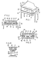
- Figure 1 is a perspective view of one end of a DIP package of the invention.
- Figure 2 is a cross-sectional view across the DIP package taken on the line 2-2 of Figure 1.
- Figure 3 is a cross-sectional view of a castellated package of the invention.
- Figure 4 is a top plan partial view of the base, preform and lead frame prior to die mounting and connection, taken on the line 4-4 of Figure 2.
- The heat-
sink package 10 which confroms in exterior configuration to a standard DIP package but having vastly improved heat rejection capabilities is seen in Figure 1. A rectangular base 11 of thermally conductive material such as copper or aluminum or alloys thereof or beryllia (BeO) having a coefficient of thermal conductivity of at least 1.0467 joules per sec. per cm per °C (0.25 cal/°C s cm), has an exterior dimension substantially the same as a standard DIP package. Standard packages vary in size dependent on the number of input/output terminals in flat contacts extending therefrom for example 16, 20 and 24 terminals. Within each number of terminals the dimensions can slightly vary generally, for example, a 20 terminal package being in the range of 22 mm to 26 mm in horizontal length, 6 mm to 8 mm in width and 6.9 mm to 7.5 mm in height. These are designated by the legends L, W and H in Figure 1. An insulative preform orannular ring 15 of epoxy, glass prepreg such as Ablefilm (trademark of Able Stick Laboratory, Gardena, California) #561 K or 550K, or other electrically insulative material is bonded by epoxy resin orother adhesive 16 around the periphery of a finite die-attach area 13 on the top surface of base 11. Alead frame 17 of copper, NILO alloy 42 (42% Ni balance Fe) or other conductive material is placed over and bonded by epoxy glass prepreg to the top of the preform extending over the length and width of the base 11. The lead frame is of conventional construction comprising a series of conductive fingers having inner ends extending inwardly of the inner periphery of the preform andouter ends 19 extending outwardly of the preform and base 11. The fingers are interconnected during manufacture by scored breakaway links 25 (Figure 4) and remain so in initial assembly operations of the package. The bottom of the die containing the integrated circuit is mounted by suitable conductive adhesive such as silver filled epoxy or silver filled glass, to the flat die-attach area of base 11 and the inner fingers bonded by wire bonds to contact pads on the upper surface of the die. After wire bonding the interconnections between the lead frame fingers are physically removed by a stamping or punching operation. An insulative plastic orceramic cap 22 is bonded by epoxy, polyimide or other insulative adhesive to the top offingers 17 and to the preform in the space between the fingers. After this operation, the interconnections 25 of the lead frame may be trimmed away and the fingers formed or bent as required. - The attachment of
bond wires 20 betweencontact pads 21 on the periphery of die 12 to theinner ends 18 oflead frame fingers 17 and the positioning ofbonding layers Bond wires 20 may be gold, gold alloy or other conventionally used wires of from about 0.635 to 1.016 mm (0.025 to 0.04 inches) in diameter bonded to the die contact pads by conventional means such as thermosonic or thermocompression bonding. Thebonding layer 14 is a heat conductive layer of silver or copper- plastic containing a high proportion of conductive particles of silver or copper and having a coefficient of thermal conductivity of at least
preform 15 preferably has a thickness of 0.127 mm (5 mil), i.e., a thickness approximately that of thedie 12 so that the top surface of the lead frame extends coplanar with thedie contact pads 20. - Figure 3 shows a castellated
package 40 in whichinner ends 33 oflead frame 32 are wire bonded to contact pads on die 12.Outer ends 34 of the frame are bent upward betweencastellations 31 integral with the top periphery ofcap 30. The aluminum base 11, its sides 11 a, and bottom 11b are completely exposed to ambient when assembled on the connector and printed circuit board. The lead fingers from the frame in other embodiments may extend outwardly of the package inthe same plane as the interior parts of the frame or may be bent up or down depending on the type of connection or plug-in desired. - Figure 4 shows aluminum base 11 in dotted lines with insulation preform 15 having an aperture 15a exposing the die-
attach area 13 of the base 11. Thelead frame 17 is placed and bonded to the preform with theends 18 of the lead frame fingers extending just beyond the preform aperture edges planar to contact pads of the die to be inserted in the preform aperture and bonded to the die-attach portion 13 of base 11. - Thermal measurements were made on a DIP device constructed in accord with Figures 1 and 2 utilizing 24 input/output leads on a copper lead frame. The base was made of an aluminum material available from Alcoa. The cap was constructed of alumina ceramic material, such as available from Narumics Inc.
- Dimensions of the aluminum base were


- The molded dual in-line packages were mounted in zero insertion force sockets and placed transverse to the air stream in a wind tunnel. Samples were tested at various air flows and static zero air flow which was theoretically the worst case tested. Thermocouples were mounted directly to the aluminum bottom of the package. The thermal impedance of the device is defined as the rise in junction temperature against a reference point per unit of power dissipation. The temperature of the hottest junction on the die under power dissipation is measured using a substrate diode to monitor chip temperature. The thermal impedance 8cA (case to ambient) is denoted by the formula:

- °CB is the case base temperature °C under power and stablized.
- °CA is the ambient temperature and
- Pd is the power dissipated by the device which=Icc×Ccc, where
- Vee is the device voltage supplied by the power supply and
- Ice is the supply current.
- θJA, the total thermal resistance from the semiconductor junction to the ambient equals ΔcA+θJC where 6Jc (the thermal resistance from the junction to the case) may be considered a constant since its effect on θJA is small namely about 3 to 4°C/watt in devices tested. Four watts of power were furnished to two specimen packages.
- A first sample package of a prior art configuration 24 J 600 chosen to be as close to the sample package of the invention as possible in number of leads, type of lead frame, die size, etc. resulted in a measured static air


- As can be seen above, the package of this invention efficiently rejects that generated within a package which utilizes a standard lead frame and standard dimensions of the components (base and cap) used in a standard DIP package. The device may use existing plastic molds, standard trim and form procedures and utilize standard printed circuit board assembly machinery for assembly of the package to the board or other substrate. Likewise, the heat-rejecting DIP packages can be stored, shipped and utilized in assembly operations in and from standard shipping rails.
Claims (12)
Applications Claiming Priority (2)
| Application Number | Priority Date | Filing Date | Title |
|---|---|---|---|
| US62040184A | 1984-06-14 | 1984-06-14 | |
| US620401 | 1984-06-14 |
Publications (3)
| Publication Number | Publication Date |
|---|---|
| EP0164794A2 EP0164794A2 (en) | 1985-12-18 |
| EP0164794A3 EP0164794A3 (en) | 1987-03-04 |
| EP0164794B1 true EP0164794B1 (en) | 1990-07-25 |
Family
ID=24485779
Family Applications (1)
| Application Number | Title | Priority Date | Filing Date |
|---|---|---|---|
| EP85200826A Expired - Lifetime EP0164794B1 (en) | 1984-06-14 | 1985-05-22 | Multi-layer heat sinking integrated circuit package |
Country Status (3)
| Country | Link |
|---|---|
| EP (1) | EP0164794B1 (en) |
| JP (1) | JPH0789576B2 (en) |
| DE (1) | DE3578830D1 (en) |
Families Citing this family (13)
| Publication number | Priority date | Publication date | Assignee | Title |
|---|---|---|---|---|
| EP0273556A1 (en) * | 1986-12-22 | 1988-07-06 | Trw Inc. | Integrated-circuit chip packaging construction |
| US5139973A (en) * | 1990-12-17 | 1992-08-18 | Allegro Microsystems, Inc. | Method for making a semiconductor package with the distance between a lead frame die pad and heat spreader determined by the thickness of an intermediary insulating sheet |
| US5652461A (en) * | 1992-06-03 | 1997-07-29 | Seiko Epson Corporation | Semiconductor device with a convex heat sink |
| JP3572628B2 (en) * | 1992-06-03 | 2004-10-06 | セイコーエプソン株式会社 | Semiconductor device and manufacturing method thereof |
| JP3362530B2 (en) * | 1993-12-16 | 2003-01-07 | セイコーエプソン株式会社 | Resin-sealed semiconductor device and method of manufacturing the same |
| US6466446B1 (en) | 1994-07-01 | 2002-10-15 | Saint Gobain/Norton Industrial Ceramics Corporation | Integrated circuit package with diamond heat sink |
| JP3509274B2 (en) * | 1994-07-13 | 2004-03-22 | セイコーエプソン株式会社 | Resin-sealed semiconductor device and method of manufacturing the same |
| JP3367299B2 (en) * | 1994-11-11 | 2003-01-14 | セイコーエプソン株式会社 | Resin-sealed semiconductor device and method of manufacturing the same |
| JP3542677B2 (en) * | 1995-02-27 | 2004-07-14 | セイコーエプソン株式会社 | Resin-sealed semiconductor device and method of manufacturing the same |
| JP3309686B2 (en) * | 1995-03-17 | 2002-07-29 | セイコーエプソン株式会社 | Resin-sealed semiconductor device and method of manufacturing the same |
| US6841857B2 (en) * | 2001-07-18 | 2005-01-11 | Infineon Technologies Ag | Electronic component having a semiconductor chip, system carrier, and methods for producing the electronic component and the semiconductor chip |
| US20160269794A1 (en) | 2013-10-01 | 2016-09-15 | Dentsu Inc. | Multi-view video layout system |
| JP5794292B2 (en) * | 2013-12-27 | 2015-10-14 | 第一精工株式会社 | Electrical connector |
Family Cites Families (7)
| Publication number | Priority date | Publication date | Assignee | Title |
|---|---|---|---|---|
| US4195193A (en) * | 1979-02-23 | 1980-03-25 | Amp Incorporated | Lead frame and chip carrier housing |
| CA1188010A (en) * | 1981-05-06 | 1985-05-28 | Leonard W. Schaper | Package for a semiconductor chip |
| JPS5817649A (en) * | 1981-07-24 | 1983-02-01 | Fujitsu Ltd | Package for electronic part |
| US4401767A (en) * | 1981-08-03 | 1983-08-30 | Johnson Matthey Inc. | Silver-filled glass |
| FR2529385B1 (en) * | 1982-06-29 | 1985-12-13 | Thomson Csf | MICROBOX FOR LOGIC INTEGRATED CIRCUITS OPERATING AT VERY HIGH FREQUENCY |
| CA1201211A (en) * | 1982-08-05 | 1986-02-25 | Olin Corporation | Hermetically sealed semiconductor casing |
| JPS59224146A (en) * | 1983-06-03 | 1984-12-17 | Oki Electric Ind Co Ltd | Semiconductor device |
-
1985
- 1985-05-22 EP EP85200826A patent/EP0164794B1/en not_active Expired - Lifetime
- 1985-05-22 DE DE8585200826T patent/DE3578830D1/en not_active Expired - Lifetime
- 1985-06-04 JP JP60121355A patent/JPH0789576B2/en not_active Expired - Fee Related
Also Published As
| Publication number | Publication date |
|---|---|
| EP0164794A3 (en) | 1987-03-04 |
| JPH0789576B2 (en) | 1995-09-27 |
| DE3578830D1 (en) | 1990-08-30 |
| JPS614254A (en) | 1986-01-10 |
| EP0164794A2 (en) | 1985-12-18 |
Similar Documents
| Publication | Publication Date | Title |
|---|---|---|
| US5262927A (en) | Partially-molded, PCB chip carrier package | |
| US5504372A (en) | Adhesively sealed metal electronic package incorporating a multi-chip module | |
| US6330158B1 (en) | Semiconductor package having heat sinks and method of fabrication | |
| US4870224A (en) | Integrated circuit package for surface mount technology | |
| US6482674B1 (en) | Semiconductor package having metal foil die mounting plate | |
| US6566164B1 (en) | Exposed copper strap in a semiconductor package | |
| US7619302B2 (en) | Highly efficient both-side-cooled discrete power package, especially basic element for innovative power modules | |
| US5075759A (en) | Surface mounting semiconductor device and method | |
| US5293301A (en) | Semiconductor device and lead frame used therein | |
| US8916958B2 (en) | Semiconductor package with multiple chips and substrate in metal cap | |
| EP0164794B1 (en) | Multi-layer heat sinking integrated circuit package | |
| JPH06224246A (en) | High multiterminal package for semiconductor element | |
| US7498195B2 (en) | Multi-chip semiconductor connector assembly method | |
| US5939781A (en) | Thermally enhanced integrated circuit packaging system | |
| US7102211B2 (en) | Semiconductor device and hybrid integrated circuit device | |
| US8253239B2 (en) | Multi-chip semiconductor connector | |
| EP0436126A2 (en) | Resin-encapsulated semiconductor device | |
| US20220208661A1 (en) | Qfn/qfp package with insulated top-side thermal pad | |
| KR20200070958A (en) | Semiconductor device package | |
| KR102225628B1 (en) | Plastic qfn package with improved heat characteristic | |
| CN111244061A (en) | Packaging structure of gallium nitride equipment | |
| JP2649251B2 (en) | Substrate for mounting electronic components | |
| KR20020088300A (en) | Semiconductor package with heat spreader using cooling material | |
| JPH07326690A (en) | Package for semiconductor device and semiconductor device | |
| JPH09503888A (en) | Edge-connectable metal package |
Legal Events
| Date | Code | Title | Description |
|---|---|---|---|
| PUAI | Public reference made under article 153(3) epc to a published international application that has entered the european phase |
Free format text: ORIGINAL CODE: 0009012 |
|
| AK | Designated contracting states |
Designated state(s): DE FR GB NL |
|
| PUAL | Search report despatched |
Free format text: ORIGINAL CODE: 0009013 |
|
| AK | Designated contracting states |
Kind code of ref document: A3 Designated state(s): DE FR GB NL |
|
| 17P | Request for examination filed |
Effective date: 19870806 |
|
| 17Q | First examination report despatched |
Effective date: 19890215 |
|
| RAP1 | Party data changed (applicant data changed or rights of an application transferred) |
Owner name: ADVANCED MICRO DEVICES, INC. |
|
| GRAA | (expected) grant |
Free format text: ORIGINAL CODE: 0009210 |
|
| AK | Designated contracting states |
Kind code of ref document: B1 Designated state(s): DE FR GB NL |
|
| REF | Corresponds to: |
Ref document number: 3578830 Country of ref document: DE Date of ref document: 19900830 |
|
| ET | Fr: translation filed | ||
| PLBE | No opposition filed within time limit |
Free format text: ORIGINAL CODE: 0009261 |
|
| STAA | Information on the status of an ep patent application or granted ep patent |
Free format text: STATUS: NO OPPOSITION FILED WITHIN TIME LIMIT |
|
| 26N | No opposition filed | ||
| REG | Reference to a national code |
Ref country code: GB Ref legal event code: IF02 |
|
| PGFP | Annual fee paid to national office [announced via postgrant information from national office to epo] |
Ref country code: GB Payment date: 20030401 Year of fee payment: 19 |
|
| PGFP | Annual fee paid to national office [announced via postgrant information from national office to epo] |
Ref country code: NL Payment date: 20030403 Year of fee payment: 19 |
|
| PGFP | Annual fee paid to national office [announced via postgrant information from national office to epo] |
Ref country code: FR Payment date: 20040503 Year of fee payment: 20 |
|
| PG25 | Lapsed in a contracting state [announced via postgrant information from national office to epo] |
Ref country code: GB Free format text: LAPSE BECAUSE OF NON-PAYMENT OF DUE FEES Effective date: 20040522 |
|
| PGFP | Annual fee paid to national office [announced via postgrant information from national office to epo] |
Ref country code: DE Payment date: 20040528 Year of fee payment: 20 |
|
| PG25 | Lapsed in a contracting state [announced via postgrant information from national office to epo] |
Ref country code: NL Free format text: LAPSE BECAUSE OF NON-PAYMENT OF DUE FEES Effective date: 20041201 |
|
| GBPC | Gb: european patent ceased through non-payment of renewal fee |
Effective date: 20040522 |
|
| NLV4 | Nl: lapsed or anulled due to non-payment of the annual fee |
Effective date: 20041201 |