WO2014188918A1 - 透明導電膜及び透明導電膜の製造方法 - Google Patents
透明導電膜及び透明導電膜の製造方法 Download PDFInfo
- Publication number
- WO2014188918A1 WO2014188918A1 PCT/JP2014/062783 JP2014062783W WO2014188918A1 WO 2014188918 A1 WO2014188918 A1 WO 2014188918A1 JP 2014062783 W JP2014062783 W JP 2014062783W WO 2014188918 A1 WO2014188918 A1 WO 2014188918A1
- Authority
- WO
- WIPO (PCT)
- Prior art keywords
- metal
- conductive film
- transparent conductive
- metal wiring
- support
- Prior art date
Links
Images


Classifications
-
- H—ELECTRICITY
- H05—ELECTRIC TECHNIQUES NOT OTHERWISE PROVIDED FOR
- H05K—PRINTED CIRCUITS; CASINGS OR CONSTRUCTIONAL DETAILS OF ELECTRIC APPARATUS; MANUFACTURE OF ASSEMBLAGES OF ELECTRICAL COMPONENTS
- H05K1/00—Printed circuits
- H05K1/02—Details
- H05K1/09—Use of materials for the conductive, e.g. metallic pattern
-
- H—ELECTRICITY
- H01—ELECTRIC ELEMENTS
- H01B—CABLES; CONDUCTORS; INSULATORS; SELECTION OF MATERIALS FOR THEIR CONDUCTIVE, INSULATING OR DIELECTRIC PROPERTIES
- H01B1/00—Conductors or conductive bodies characterised by the conductive materials; Selection of materials as conductors
- H01B1/02—Conductors or conductive bodies characterised by the conductive materials; Selection of materials as conductors mainly consisting of metals or alloys
-
- G—PHYSICS
- G06—COMPUTING; CALCULATING OR COUNTING
- G06F—ELECTRIC DIGITAL DATA PROCESSING
- G06F3/00—Input arrangements for transferring data to be processed into a form capable of being handled by the computer; Output arrangements for transferring data from processing unit to output unit, e.g. interface arrangements
- G06F3/01—Input arrangements or combined input and output arrangements for interaction between user and computer
- G06F3/03—Arrangements for converting the position or the displacement of a member into a coded form
- G06F3/041—Digitisers, e.g. for touch screens or touch pads, characterised by the transducing means
- G06F3/045—Digitisers, e.g. for touch screens or touch pads, characterised by the transducing means using resistive elements, e.g. a single continuous surface or two parallel surfaces put in contact
-
- G—PHYSICS
- G09—EDUCATION; CRYPTOGRAPHY; DISPLAY; ADVERTISING; SEALS
- G09F—DISPLAYING; ADVERTISING; SIGNS; LABELS OR NAME-PLATES; SEALS
- G09F9/00—Indicating arrangements for variable information in which the information is built-up on a support by selection or combination of individual elements
-
- H—ELECTRICITY
- H05—ELECTRIC TECHNIQUES NOT OTHERWISE PROVIDED FOR
- H05K—PRINTED CIRCUITS; CASINGS OR CONSTRUCTIONAL DETAILS OF ELECTRIC APPARATUS; MANUFACTURE OF ASSEMBLAGES OF ELECTRICAL COMPONENTS
- H05K1/00—Printed circuits
- H05K1/02—Details
- H05K1/0296—Conductive pattern lay-out details not covered by sub groups H05K1/02 - H05K1/0295
-
- H—ELECTRICITY
- H05—ELECTRIC TECHNIQUES NOT OTHERWISE PROVIDED FOR
- H05K—PRINTED CIRCUITS; CASINGS OR CONSTRUCTIONAL DETAILS OF ELECTRIC APPARATUS; MANUFACTURE OF ASSEMBLAGES OF ELECTRICAL COMPONENTS
- H05K3/00—Apparatus or processes for manufacturing printed circuits
- H05K3/02—Apparatus or processes for manufacturing printed circuits in which the conductive material is applied to the surface of the insulating support and is thereafter removed from such areas of the surface which are not intended for current conducting or shielding
- H05K3/027—Apparatus or processes for manufacturing printed circuits in which the conductive material is applied to the surface of the insulating support and is thereafter removed from such areas of the surface which are not intended for current conducting or shielding the conductive material being removed by irradiation, e.g. by photons, alpha or beta particles
-
- H—ELECTRICITY
- H05—ELECTRIC TECHNIQUES NOT OTHERWISE PROVIDED FOR
- H05K—PRINTED CIRCUITS; CASINGS OR CONSTRUCTIONAL DETAILS OF ELECTRIC APPARATUS; MANUFACTURE OF ASSEMBLAGES OF ELECTRICAL COMPONENTS
- H05K3/00—Apparatus or processes for manufacturing printed circuits
- H05K3/10—Apparatus or processes for manufacturing printed circuits in which conductive material is applied to the insulating support in such a manner as to form the desired conductive pattern
-
- H—ELECTRICITY
- H10—SEMICONDUCTOR DEVICES; ELECTRIC SOLID-STATE DEVICES NOT OTHERWISE PROVIDED FOR
- H10K—ORGANIC ELECTRIC SOLID-STATE DEVICES
- H10K71/00—Manufacture or treatment specially adapted for the organic devices covered by this subclass
- H10K71/60—Forming conductive regions or layers, e.g. electrodes
-
- H—ELECTRICITY
- H05—ELECTRIC TECHNIQUES NOT OTHERWISE PROVIDED FOR
- H05K—PRINTED CIRCUITS; CASINGS OR CONSTRUCTIONAL DETAILS OF ELECTRIC APPARATUS; MANUFACTURE OF ASSEMBLAGES OF ELECTRICAL COMPONENTS
- H05K2201/00—Indexing scheme relating to printed circuits covered by H05K1/00
- H05K2201/03—Conductive materials
- H05K2201/0332—Structure of the conductor
- H05K2201/0364—Conductor shape
-
- H—ELECTRICITY
- H05—ELECTRIC TECHNIQUES NOT OTHERWISE PROVIDED FOR
- H05K—PRINTED CIRCUITS; CASINGS OR CONSTRUCTIONAL DETAILS OF ELECTRIC APPARATUS; MANUFACTURE OF ASSEMBLAGES OF ELECTRICAL COMPONENTS
- H05K2201/00—Indexing scheme relating to printed circuits covered by H05K1/00
- H05K2201/09—Shape and layout
- H05K2201/09209—Shape and layout details of conductors
-
- H—ELECTRICITY
- H05—ELECTRIC TECHNIQUES NOT OTHERWISE PROVIDED FOR
- H05K—PRINTED CIRCUITS; CASINGS OR CONSTRUCTIONAL DETAILS OF ELECTRIC APPARATUS; MANUFACTURE OF ASSEMBLAGES OF ELECTRICAL COMPONENTS
- H05K2203/00—Indexing scheme relating to apparatus or processes for manufacturing printed circuits covered by H05K3/00
- H05K2203/05—Patterning and lithography; Masks; Details of resist
- H05K2203/0502—Patterning and lithography
-
- H—ELECTRICITY
- H10—SEMICONDUCTOR DEVICES; ELECTRIC SOLID-STATE DEVICES NOT OTHERWISE PROVIDED FOR
- H10K—ORGANIC ELECTRIC SOLID-STATE DEVICES
- H10K50/00—Organic light-emitting devices
- H10K50/80—Constructional details
- H10K50/805—Electrodes
- H10K50/81—Anodes
- H10K50/814—Anodes combined with auxiliary electrodes, e.g. ITO layer combined with metal lines
-
- Y—GENERAL TAGGING OF NEW TECHNOLOGICAL DEVELOPMENTS; GENERAL TAGGING OF CROSS-SECTIONAL TECHNOLOGIES SPANNING OVER SEVERAL SECTIONS OF THE IPC; TECHNICAL SUBJECTS COVERED BY FORMER USPC CROSS-REFERENCE ART COLLECTIONS [XRACs] AND DIGESTS
- Y10—TECHNICAL SUBJECTS COVERED BY FORMER USPC
- Y10T—TECHNICAL SUBJECTS COVERED BY FORMER US CLASSIFICATION
- Y10T29/00—Metal working
- Y10T29/49—Method of mechanical manufacture
- Y10T29/49002—Electrical device making
- Y10T29/49117—Conductor or circuit manufacturing
- Y10T29/49124—On flat or curved insulated base, e.g., printed circuit, etc.
- Y10T29/49155—Manufacturing circuit on or in base
Definitions
- the present invention relates to a transparent conductive film and a method for producing the transparent conductive film.
- Metal is suitable for use as a conductive layer material because of its high conductivity, but strongly reflects visible light, so it is unsuitable for applications where the electrode pattern is visible, such as a touch panel. It is. Thus, conventionally, transparent conductive oxides such as ITO (Indium Tin Oxide) have been used for these applications.
- ITO Indium Tin Oxide
- metals are advantageous in that they are easier to pattern than oxides, have excellent flexibility, and have low resistance, they are being studied as alternative materials for ITO. In recent years, it has been found that the problem of visually recognizing metal wiring can be reduced to some extent by thinning the metal wires and devising the pattern.
- a conductive layer is formed by laminating a blackened layer having a thickness of 0.01 to 0.5 ⁇ m on the surface of the conductive pattern layer.
- a method for preventing pattern reflection is disclosed.
- the technique according to Japanese Patent Application Laid-Open No. 2011-082221 has a problem that a decrease in conductivity cannot be avoided in principle.
- a technique for imparting antiglare properties to an antireflection film has been known (see Japanese Patent Application Laid-Open Nos. 2005-070435 and 2004-004404).
- the fine metal wire is light reflection peculiar to the metal, it is easy to see the fine metal wire in the transparent conductive film or the like, and the pattern by the fine metal wire is easy to see.
- the fine metal wires have been thinned and the pattern has been devised, but the electrical resistance tends to increase. Therefore, if the volume ratio of the metal is increased by calendering or the like in order to reduce the resistance, the light reflection is remarkably increased, and it is difficult to achieve both visibility (the wiring pattern is difficult to see) and low resistance. It was.
- the present invention has been made in consideration of such problems, and by defining the surface shape of the fine metal wire, it is possible to achieve both visibility and low resistance, and it can be used for touch panels and display devices.
- An object is to provide a suitable transparent conductive film.
- Another object of the present invention is to provide a transparent conductive film capable of improving both the visibility of the transparent conductive film and reducing the electrical resistance by making the pressing surface of the calendar an appropriate material and surface form. It is to provide a manufacturing method.
- Another object of the present invention is to provide a highly reliable touch panel because the wiring pattern is difficult to see even when installed on a display screen, and the electrical resistance is low and the adhesion of the wiring is good. There is.
- Another object of the present invention is that in a display device in which a transparent conductive film is installed on a display screen, the wiring pattern of the transparent conductive film is difficult to see, the electrical resistance is low, and the wiring adhesion is good. Another object is to provide a highly reliable display device.
- the inventors of the present invention applied a method for imparting antiglare properties to a sample by pressing a surface having a concavo-convex surface against the sample surface (see JP-A-2005-070435, etc.) and a photosensitive material having a silver salt emulsion layer. Investigation was started to apply to a transparent conductive film produced by exposure and development.
- the present invention has the following configuration.
- the transparent conductive film according to the first aspect of the present invention is a transparent conductive film having a support and a metal wiring part formed on the support, wherein at least a part of the metal wiring part is Ra 2 / It has a surface shape satisfying Sm> 0.01 ⁇ m and has a metal volume ratio of 35% or more.
- Ra is an arithmetic average roughness [ ⁇ m] and is equal to or less than the thickness of the metal wiring at the surface roughness measurement location.
- Sm is an average interval [ ⁇ m] of the unevenness, and is 0.01 ⁇ m or more. The same applies hereinafter.
- the surface of the metal wiring part is a glossy surface, visible light is strongly reflected, and the proportion of regular reflection light (regular reflectance) in the reflected light is increased.
- regular reflectance regular reflectance
- the metal volume ratio of the fine metal wire is low, incident light enters between the metal particles, so that the regular reflectance is reduced, but there is a problem that the electrical resistance is increased because the metal particles are poorly contacted. Therefore, in order to reduce the electrical resistance of the fine metal wires, when the volume ratio of the metal is increased by calendering or the like, the metal particles on the surface are densely arranged, so that the regular reflectance is remarkably increased. The problem of being noticeable arises. That is, it is difficult to achieve both visibility (thin metal wires are inconspicuous) and low resistance.
- At least a part of the metal wiring portion has a surface shape that satisfies Ra 2 /Sm>0.01 ⁇ m.
- the metal volume ratio is 35% or more, light reflection at the metal wiring portion can be suppressed. That is, it is possible to achieve both visibility (the metal fine wire is not noticeable) and low resistance.
- the surface shape (surface roughness) in the present invention a value measured with a measuring instrument having a height and a horizontal spatial resolution higher than 0.03 ⁇ m is adopted. Specifically, a laser microscope having an objective lens of 100 times or more is used. The measurement range is 100 ⁇ m or more and 300 ⁇ m or less.
- the stylus type surface roughness meter has a low spatial resolution and cannot measure the surface roughness defined in the present invention.
- Sm of at least a part of the metal wiring portion is 4 ⁇ m or less.
- the regular reflectance can be suppressed to 1.2% or less.
- the difference between the regular reflectance of at least a part of the surface of the metal wiring portion and the regular reflectance of the back surface of the metal wiring portion is preferably less than 3%.
- the back surface means the surface of the metal wiring portion observed through the support from the surface opposite to the surface on which the metal wiring portion is disposed.
- the regular reflectance is obtained by subtracting the reflectance that occurs at the interface between air and the support.
- metal wiring portions first metal wiring portion and second metal wiring portion
- the difference between the regular reflectance of the surface of the first metal wiring portion in the transparent conductive film and the regular reflectance of the back surface of the second metal wiring portion on the side observed through the support is less than 3%. From this, when the metal fine wire which comprises a 1st metal wiring part becomes difficult to visually recognize, it becomes difficult to visually recognize the metal fine wire which comprises a 2nd metal wiring part. As a result, even in the transparent conductive film in which the metal wiring portions are formed on the front surface and the back surface of one support, visibility is improved, and the resistance of the first metal wiring portion and the second metal wiring portion is reduced. Can do.
- a step of forming a metal wiring part on a support and a metal member having irregularities on the surface are pressed against at least a part of the metal wiring part.
- the surface shape of the metal member is characterized in that Ra 2 / Sm is larger than 0.015 ⁇ m.
- the metal wiring part has a surface shape satisfying Ra 2 /Sm>0.01 ⁇ m, and a transparent conductive film having a metal volume ratio of 35% or more can be easily produced.
- a step of forming a metal wiring part on a support and a metal member having irregularities on the surface are pressed against at least a part of the metal wiring part.
- the surface shape of the metal member has a calender process, and Sm is equal to or less than the line width of the fine metal wire constituting at least a part of the metal wiring portion, and Ra is equal to or less than 1/6 of the thickness of the fine metal wire before the calender process. And Ra 2 / Sm is greater than 0.015 ⁇ m.
- At least a part of the metal wiring part has Sm of 4 ⁇ m or less, at least a part of the metal wiring part has a surface shape satisfying Ra 2 /Sm>0.01 ⁇ m, and the metal volume ratio is 35%.
- the transparent conductive film as described above can be easily produced.
- a method for producing a transparent conductive film according to a fourth aspect of the present invention includes a step of forming a metal wiring portion on a support and a resin plate having irregularities on the surface is pressed against at least a part of the metal wiring portion.
- the surface shape of the resin plate is characterized in that Ra is larger than 0.15 ⁇ m.
- the resin plate also includes a resin film.
- Ra 2 / Sm is preferably larger than 0.01 ⁇ m.
- at least a part of the metal wiring part has Sm of 4 ⁇ m or less, at least a part of the metal wiring part has a surface shape satisfying Ra 2 /Sm>0.01 ⁇ m, and the metal volume ratio is 35%.
- the transparent conductive film as described above can be easily produced.
- the method for producing a transparent conductive film according to the fifth aspect of the present invention includes a step of forming a metal wiring part on a support having irregularities on the surface, and the surface of the support has a Ra of 0. It is larger than 15 ⁇ m.
- the uneven shape on the surface of the support is transferred to the surface of the metal wiring part. That is, even in the method of forming a metal wiring part on a support having an uneven surface, at least a part of the metal wiring part has a surface shape satisfying Ra 2 /Sm>0.01 ⁇ m and has a metal volume ratio. Can achieve a characteristic of 35% or more. As a result, it is possible to obtain a transparent conductive film having better visibility than when a metal film is formed on a smooth surface.
- the step of forming the metal wiring portion on the support may include a step of depositing metal on the surface of the support.
- the transparent conductive film in which the metal wiring portion has a surface shape satisfying Ra 2 /Sm>0.01 ⁇ m and the metal volume ratio is 35% or more can be obtained.
- the step of forming the metal wiring portion on the support may include a step of plating the metal on the surface of the support.
- a transparent conductive film in which the metal wiring portion has a surface shape satisfying Ra 2 /Sm>0.01 ⁇ m and the metal volume ratio is 35% or more can be obtained.
- the metal wiring part may have a mesh pattern made of fine metal wires at least partially.
- a transparent conductive film according to a sixth aspect of the present invention is manufactured by the method for manufacturing a transparent conductive film according to the second to fifth aspects of the invention described above.
- At least a part of the metal wiring portion may have a mesh pattern made of fine metal wires.
- a touch panel according to a seventh aspect of the present invention includes the transparent conductive film according to the first or sixth aspect of the present invention.
- the wiring pattern is difficult to see, the electrical resistance is low, and the wiring has good adhesion, so that a highly reliable touch panel can be obtained.
- a display device includes the transparent conductive film according to the first or sixth aspect of the present invention.
- the wiring pattern of the transparent conductive film is difficult to see, and since the electrical resistance is low and the wiring adhesion is good, the display has high reliability. A device can be obtained.
- the transparent conductive film according to the present invention it is possible to achieve both visibility and low resistance by defining the surface shape of the fine metal wire, and use it for a touch panel or a display device. Preferred.
- the improvement of the visibility of a transparent conductive film and reduction of an electrical resistance are compatible by making the pushing surface of a calendar into an appropriate material and surface form. Can do.
- the touch panel of the present invention even if it is installed on a display screen, the wiring pattern is difficult to see, and the electrical resistance is low, and furthermore, the adhesion of the wiring is high, so that the reliability is high. .
- the display device in the display device in which the transparent conductive film is installed on the display screen, the wiring pattern of the transparent conductive film is difficult to see, and the electric resistance is low, and further, the adhesion of the wiring is low. To be good, it becomes highly reliable.
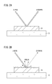
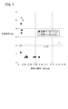
- FIG. 1A is a cross-sectional view showing a partially omitted transparent conductive film according to the present embodiment installed on a display panel of a display device
- FIG. 1B is a plan view showing a partially omitted transparent conductive film.
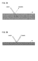
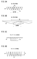
- FIG. 2A is an explanatory view showing the action of a normal fine metal wire having a glossy surface (high specular reflection light rate)
- FIG. 2B is a diagram of the fine metal wire according to the present embodiment having a rough surface. It is explanatory drawing which shows an effect
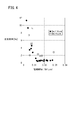
- FIG. 3A is an explanatory diagram showing the action of a normal metal fine wire with a low metal volume ratio (low specular reflection efficiency), and FIG.
- FIG. 3B shows the action of a normal metal fine wire with a high metal volume ratio (high specular reflection efficiency). It is explanatory drawing shown. It is a graph showing a plot of the change in specular reflectance for Ra 2 / Sm of the electrode portion.
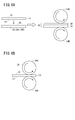
- FIG. 5A is a cross-sectional view illustrating a configuration in which metal wiring portions (first metal wiring portion and second metal wiring portion) are respectively formed on the front surface and the back surface of one transparent substrate, and FIG. It is sectional drawing which abbreviate
- FIG. 6A is an explanatory diagram showing a first method of calendar processing, and FIG.
- 6B is an explanatory diagram showing a second method of calendar processing.
- the Sm of the metal roller is less than or equal to the line width of the fine metal wire, and when the Sm of the metal roller is larger than the line width of the fine metal wire, the change in regular reflectance with respect to Ra 2 / Sm of the pressing surface of the metal roller is plotted. It is a graph shown.
- 8A and 8B are explanatory diagrams showing the relationship between the Sm of the metal plate or metal roller and the line width of the thin metal wire
- FIGS. 8C and 8D are the relationship between Ra of the metal plate or metal roller and the thickness of the thin metal wire. It is explanatory drawing which shows.
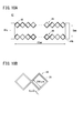
- FIG. 10A is a plan view showing a mesh pattern electrode formed on a mesh sample
- FIG. 10B is a plan view showing the size of a square lattice constituting the mesh pattern electrode.
- the horizontal axis represents Ra of the pressing surface of the metal plate
- the vertical axis represents Sm of the pressing surface
- Examples 1 to 3, Comparative Examples 3 to 6, 13, 14, and Comparative Examples 7 to 11 are plotted. It is a graph shown.
- FIGS. 1A to 11 embodiments of a transparent conductive film, a manufacturing method thereof, a touch panel, and a display device according to the present invention will be described with reference to FIGS. 1A to 11.
- ⁇ indicating a numerical range is used as a meaning including numerical values described before and after the numerical value as a lower limit value and an upper limit value.
- the transparent conductive film 10 includes a transparent substrate 12 (support) and a metal wiring portion 14 formed on the surface 12a of the transparent substrate 12, for example, It is stuck on the display panel 16a of the display device 16. That is, the transparent conductive film 10 is used, for example, as an electromagnetic wave shielding film of the display device 16 or a transparent conductive film for a touch panel.
- the display device 16 include a liquid crystal display, a plasma display, an organic EL (electroluminescence), and an inorganic EL.
- the transparent conductive film 10 can be applied to the inside of the display device 16 and used integrally with the display device 16.
- the metal wiring part 14 includes, for example, an electromagnetic wave shielding film or an electrode part 18 that constitutes an electrode of a touch panel, and a number of metal wirings 20 that supply a drive signal to the electrode part 18 or transmit a signal from the electrode part 18.
- Wiring part 22 For example, as shown in FIG. 1B, the electrode unit 18 has a mesh pattern 28 in which a large number of lattices 26 made of thin metal wires 24 are arranged.
- the metal wiring 20 and the thin metal wire 24 are made of a metal whose main component is, for example, gold (Au), silver (Ag), or copper (Cu).
- the line width Wa of the metal wiring 20 and the line width Wb of the metal thin wire 24 have a relationship of Wa ⁇ Wb
- the thickness ta of the metal wiring 20 and the thickness tb of the metal thin wire 24 have a relationship of ta ⁇ tb
- the length La of one side of the grating 26 by the fine metal wires 24 constituting the electrode portion 18 is preferably 100 to 400 ⁇ m or less, more preferably 150 to 300 ⁇ m, and most preferably 210 to 250 ⁇ m or less.
- the length La of one side of the lattice 26 is in the above range, it is possible to keep the transparency better, and when the display device 16 is mounted on the display panel 16a of the display device 16, the display can be visually recognized without a sense of incongruity. be able to.
- Examples of the shape of the lattice 26 include a square, a rectangle, a parallelogram, a rhombus, and a polygon such as a hexagon and an octagon.
- the line width Wb of the fine metal wire 24 can be selected from 30 ⁇ m or less.
- the line width Wb of the thin metal wire 24 is preferably 1 ⁇ m to 20 ⁇ m, more preferably 1 ⁇ m to 9 ⁇ m, and further preferably 2 ⁇ m to 7 ⁇ m.
- the line width Wb of the thin metal wire 24 is preferably 0.1 ⁇ m or more and 15 ⁇ m or less, more preferably 1 ⁇ m or more and 9 ⁇ m or less, and further preferably 2 ⁇ m or more and 7 ⁇ m or less.
- the transparent conductive film 10 according to the present embodiment can also be applied to a projected capacitive touch panel, a surface capacitive touch panel, and a resistive touch panel. Moreover, it can utilize also as an optical film installed in the display panel 16a of the display apparatus 16. FIG.
- At least the electrode portion 18 of the metal wiring portion 14 has a surface shape satisfying Ra 2 /Sm>0.01 ⁇ m, and the metal volume ratio is 35. % Or more.
- Ra is an arithmetic average roughness [ ⁇ m] and is equal to or less than the thickness of the metal wiring at the surface roughness measurement location.
- Sm is an average interval [ ⁇ m] of the unevenness, and is 0.01 ⁇ m or more.
- the metal volume ratio is calculated using the metal amount M [g / m 2 ] per unit area, the specific gravity d [g / m 3 ] of the metal, and the average film thickness H [m] measured by the cross-sectional SEM image. .
- the fine metal wire 24 refers to a layer in which a metal is continuously connected without including an undercoat layer and an overcoat layer.
- the average thickness H is the average value measured by observing the cross-sectional form in a range of at least 1 mm in total. The higher the metal volume ratio, the lower the volume resistance. However, if the metal volume fraction is too high, metal reflection may not be suppressed even if the surface shape is optimized.
- the metal volume ratio is preferably 35% or more, more preferably 50% or more, further preferably 50% or more and 80% or less, and particularly preferably 55% or more and 65% or less.
- the fine metal wire may have a metal volume fraction that changes in the thickness direction, and the metal volume fraction in the vicinity of the surface is preferably lower than the metal volume fraction at the center.
- the surface of the fine metal wire 24 is a glossy surface, as shown in FIG. 2A, visible light is strongly reflected, and the proportion of regular reflection light (regular reflectance) in the reflected light increases. As a result, there is a problem that the fine metal wires 24 are easily visually recognized. Further, when the metal volume ratio of the thin metal wires 24 is low, as shown in FIG. 3A, the incident light enters between the metal particles, so that the regular reflectance is reduced, but the electrical resistance is high because the metal particles are poorly contacted. And there is a problem that the adhesion of the wiring is deteriorated. Therefore, in order to reduce the electric resistance of the electrode part 18, it is conceivable to increase the volume ratio of the metal by calendaring or the like.
- the electrode portion 18 has a surface shape that satisfies Ra 2 /Sm>0.01 ⁇ m as in the present embodiment, as shown in FIG. 2B, the ratio of scattered light increases and regular reflection occurs. Since the rate is reduced, it is difficult to visually recognize the fine metal wires 24. Therefore, even if the metal volume ratio is 35% or more, light reflection at the electrode portion 18 can be suppressed. That is, it is possible to realize both visibility (the metal thin wire 24 is not conspicuous) and low resistance.
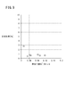
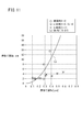
- FIG. 4 is a plot of changes in regular reflectance with respect to Ra 2 / Sm of the electrode section 18.
- the regular reflectance can be suppressed to 1.2% or less.
- the difference between the regular reflectance on the surface of the electrode portion 18 and the regular reflectance on the back surface of the electrode portion 18 is preferably less than 3%, more preferably less than 1%, and more preferably 0.5%. Less than is more preferable.
- the back surface means the surface of the electrode portion 18 observed through the transparent substrate 12 from the surface opposite to the surface on which the electrode portion 18 is disposed.
- the regular reflectance is obtained by subtracting the reflectance occurring at the interface between air and the transparent substrate 12.
- metal wiring portions first metal wiring portion 14A and second metal wiring portion 14B are formed on the front and back surfaces of one transparent substrate 12, respectively.
- the difference between the regular reflectance of the surface of the first electrode portion 18A in the transparent conductive film 10 and the regular reflectance of the back surface of the second electrode portion 18B on the side observed through the transparent substrate 12 is less than 3%. From this, when it becomes difficult to visually recognize the thin metal wire 24 constituting the first electrode portion 18A, the fine metal wire 24 constituting the second electrode portion 18B is also difficult to visually recognize. As a result, even in a transparent conductive film in which metal wiring portions are formed on the front and back surfaces of one transparent substrate 12, the visibility is improved, and the resistance of the first electrode portion 18A and the second electrode portion 18B is reduced. Can do.
- stacked two transparent conductive films (1st transparent conductive film 10A and 2nd transparent conductive film 10B) is also considered.
- both the regular reflectance of the surface of the first electrode portion 18A in the first transparent conductive film 10A and the regular reflectance of the surface of the second electrode portion 18B in the second transparent conductive film 10B are suppressed.
- a light-sensitive material having an emulsion layer containing a photosensitive silver halide salt is exposed to a transparent substrate 12, and subjected to a development treatment, whereby an exposed area and an unexposed area are respectively exposed.
- the metal wiring part 14 may be formed by forming a metal silver part and a light transmissive part.
- the entire layer in which the conductive metal is supported on the metallic silver portion is referred to as a conductive metallic portion.
- a photosensitive pre-plated layer is formed on the transparent substrate 12 using a pre-plating treatment material, and then exposed and developed, followed by plating, thereby exposing the exposed portion and the unexposed portion to metal portions and light, respectively.
- the metal wiring part 14 may be formed by forming a transparent part. Further, a conductive metal may be supported on the metal part by further performing physical development and / or plating treatment on the metal part.
- a plated layer containing a functional group that interacts with the plating catalyst or its precursor is applied on the transparent substrate 12, and then exposed and developed, and then plated to form a metal part on the material to be plated. A mode to be made.
- the photoresist film on the copper foil formed on the transparent substrate 12 is exposed and developed to form a resist pattern, and the copper foil exposed from the resist pattern is etched to form a metal wiring portion. 14 may be formed.
- the metal wiring portion 14 may be formed by printing a paste containing metal fine particles on the transparent substrate 12.
- a photoresist film is formed on the metal film, and then the photoresist film is exposed and developed to form a mask pattern, which is exposed from the mask pattern.
- the metal wiring part 14 may be formed by etching.
- the metal wiring portion 14 may be printed and formed on the transparent substrate 12 by a screen printing plate or a gravure printing plate.
- the metal wiring part 14 may be formed on the transparent substrate 12 by inkjet.
- the method for producing the transparent conductive film 10 using a silver halide photographic light-sensitive material includes the following three forms depending on the light-sensitive material and the form of development processing.
- a photosensitive silver halide black-and-white photosensitive material that does not contain physical development nuclei and an image-receiving sheet having a non-photosensitive layer that contains physical development nuclei are overlapped and transferred to develop a non-photosensitive image-receiving sheet. Form formed on top.
- the above aspect (1) is an integrated black-and-white development type, and a light-transmitting conductive film such as a light-transmitting conductive film is formed on the photosensitive material.
- the resulting developed silver is chemically developed silver or heat developed silver, and is highly active in the subsequent plating or physical development process in that it is a filament with a high specific surface.
- the light-transmitting conductive film such as a light-transmitting conductive film is formed on the photosensitive material by dissolving silver halide grains close to the physical development nucleus and depositing on the development nucleus in the exposed portion.
- a characteristic film is formed.
- This is also an integrated black-and-white development type. Although the development action is precipitation on the physical development nuclei, it is highly active, but developed silver is a sphere with a small specific surface.
- the silver halide grains are dissolved and diffused in the unexposed area and deposited on the development nuclei on the image receiving sheet, whereby a light transmitting conductive film or the like is formed on the image receiving sheet.
- a conductive film is formed. This is a so-called separate type in which the image receiving sheet is peeled off from the photosensitive material.
- either negative development processing or reversal development processing can be selected (in the case of the diffusion transfer method, negative development processing is possible by using an auto-positive type photosensitive material as the photosensitive material).
- the type of the support is not limited as long as it can support a conductive part described later, and is preferably a transparent support, and particularly preferably a plastic film.
- the transparent conductive film of the present invention can be suitably used as a transparent conductive sheet.
- the material constituting the support examples include PET (258 ° C.), polycycloolefin (134 ° C.), polycarbonate (250 ° C.), acrylic film (128 ° C.), PEN (269 ° C.), PE (135 ° C.) , PP (163 ° C.), polystyrene (230 ° C.), polyvinyl chloride (180 ° C.), polyvinylidene chloride (212 ° C.), TAC (290 ° C.), etc. are preferable plastic films having a melting point of about 290 ° C. or less. PET, polycycloolefin, and polycarbonate are preferable. Figures in parentheses are melting points.
- the visible light transmittance (JIS R3106: 1998) of the support is preferably 85% to 100%.
- the thickness of the support is not particularly limited, it can usually be arbitrarily selected in the range of 25 to 500 ⁇ m from the viewpoint of application to applications such as touch panels and electromagnetic wave shields.
- it when it serves as a function of a touch surface in addition to the function of a support, it can be designed with a thickness exceeding 500 ⁇ m.
- One preferred embodiment of the support includes a treated support that has been subjected to at least one treatment selected from the group consisting of atmospheric pressure plasma treatment, corona discharge treatment, and ultraviolet irradiation treatment.
- a hydrophilic group such as an OH group is introduced on the surface of the treated support, and the adhesion of the conductive portion described later is further improved.
- atmospheric pressure plasma treatment is preferable in that the adhesion of the conductive portion is further improved.
- the binder part is a layer provided at least between the fine metal wires 24. As a more preferable aspect, it is preferable that the surface of the support on which the fine metal wires 24 are provided is covered with the fine metal wires 24 and the binder part.
- the binder part preferably contains a polymer different from gelatin. The definition of the polymer different from gelatin is as described later.
- gelatin is not substantially contained in the binder part.
- the fact that gelatin is not substantially contained means that the content of gelatin in the binder part is less than 0.002 mg / cm 2 in the same manner as described above, and is 0 in that ion migration is further suppressed. it is preferably .001mg / cm 2 or less, and more preferably 0.0005 mg / cm 2 or less.
- the lower limit is not particularly limited, but is preferably 0 mg / cm 2 .
- the amount of gelatin in the binder portion represents the amount of gelatin contained per unit area (m 2 ) in the projected plan view when projected from the direction perpendicular to the surface of the binder portion.
- the thickness of the binder part is not particularly limited, but it is often thinner than the thickness of the conductive thin wire part.
- the binder part may contain a component other than the polymer different from gelatin.
- a polymer different from gelatin hereinafter also simply referred to as a polymer
- a polymer containing no protein is preferable.
- a polymer that is not degraded by a proteolytic enzyme is preferable.
- acrylic resins for example, acrylic resins, styrene resins, vinyl resins, polyolefin resins, polyester resins, polyurethane resins, polyamide resins, polycarbonate resins, polydiene resins, epoxy resins, silicone resins.
- examples thereof include at least one resin selected from the group consisting of a resin, a cellulose-based polymer, and a chitosan-based polymer, or a copolymer composed of monomers constituting these resins.
- at least one resin selected from the group consisting of an acrylic resin, a styrene resin, and a polyester resin, or a copolymer or the like may be used from monomers constituting these resins.
- the polymer (copolymer) represented by the following general formula (1) is mentioned from the point which can prevent more permeation
- general formulas (A), (B), (C), and (D) each represent the following repeating unit.
- R 1 represents a methyl group or a halogen atom, preferably a methyl group, a chlorine atom, or a bromine atom.
- p represents an integer of 0 to 2, preferably 0 or 1, and more preferably 0.
- R 2 represents a methyl group or an ethyl group, and a methyl group is preferable.
- R 3 represents a hydrogen atom or a methyl group, preferably a hydrogen atom.
- L represents a divalent linking group, preferably a group represented by the following general formula (2).
- X 1 represents an oxygen atom or —NR 30 —.
- R 30 represents a hydrogen atom, an alkyl group, an aryl group, or an acyl group, and each may have a substituent (for example, a halogen atom, a nitro group, a hydroxyl group, etc.).
- R 30 is preferably a hydrogen atom, an alkyl group having 1 to 10 carbon atoms (eg, methyl group, ethyl group, n-butyl group, n-octyl group, etc.), acyl group (eg, acetyl group, benzoyl group, etc.) It is.
- Particularly preferred as X 1 is an oxygen atom or —NH—.
- X 2 represents an alkylene group, an arylene group, an alkylene arylene group, an arylene alkylene group, or an alkylene arylene alkylene group, and these groups include —O—, —S—, —OCO—, —CO—, —COO—.
- R 31 represents a linear or branched alkyl group having 1 to 6 carbon atoms, such as a methyl group, an ethyl group, and an isopropyl group.
- Preferred examples of X 2 include dimethylene group, trimethylene group, tetramethylene group, o-phenylene group, m-phenylene group, p-phenylene group, —CH 2 CH 2 OCOCH 2 CH 2 —, —CH 2 CH 2 OCO ( C 6 H 4 ) — and the like.
- r represents 0 or 1;
- q represents 0 or 1, and 0 is preferable.
- R 4 represents an alkyl group having 5 to 80 carbon atoms, an alkenyl group, or an alkynyl group, preferably an alkyl group having 5 to 50 carbon atoms, more preferably an alkyl group having 5 to 30 carbon atoms, More preferred is an alkyl group having 5 to 20 carbon atoms.
- R 5 is a hydrogen atom, a methyl group, an ethyl group, a halogen atom, or an -CH 2 COOR 6, a hydrogen atom, a methyl group, a halogen atom, -CH 2 COOR 6 are preferred, hydrogen atom, a methyl group, -CH 2 COOR 6 is more preferable, and a hydrogen atom is particularly preferable.
- R 6 represents a hydrogen atom or an alkyl group having 1 to 80 carbon atoms, and may be the same as or different from R 4.
- the number of carbon atoms in R 6 is preferably 1 to 70, more preferably 1 to 60.
- x, y, z, and w represent the molar ratio of each repeating unit.
- X is 3 to 60 mol%, preferably 3 to 50 mol%, more preferably 3 to 40 mol%.
- Y is 30 to 96 mol%, preferably 35 to 95 mol%, particularly preferably 40 to 90 mol%.
- z is 0.5 to 25 mol%, preferably 0.5 to 20 mol%, particularly preferably 1 to 20 mol%.
- w is 0.5 to 40 mol%, preferably 0.5 to 30 mol%.
- x is 3 to 40 mol%
- y is 40 to 90 mol%
- z is 0.5 to 20 mol%
- w is 0.5 to 10 mol%.
- the polymer represented by the general formula (1) is preferably a polymer represented by the following general formula (3).
- x, y, z, and w are as defined above.
- the polymer represented by the general formula (1) may include other repeating units other than the above general formulas (A), (B), (C) and (D).
- Examples of monomers for forming other repeating units include acrylic acid esters, methacrylic acid esters, vinyl esters, olefins, crotonic acid esters, itaconic acid diesters, maleic acid diesters, and fumaric acid diesters. , Acrylamides, unsaturated carboxylic acids, allyl compounds, vinyl ethers, vinyl ketones, vinyl heterocycles, glycidyl esters, unsaturated nitriles, and the like. These monomers are also described in [0010] to [0022] of Japanese Patent No. 3754745.
- Acrylic acid esters and methacrylic acid esters are preferable from the viewpoint of hydrophobicity, and hydroxyalkyl methacrylates or hydroxyalkyl acrylates such as hydroxyethyl methacrylate are more preferable.
- the polymer represented by the general formula (1) preferably includes a repeating unit represented by the following general formula (E) in addition to the above general formulas (A), (B), (C) and (D).
- L E represents an alkylene group, preferably an alkylene group having 1 to 10 carbon atoms, more preferably an alkylene group having 2 to 6 carbon atoms, and further preferably an alkylene group having 2 to 4 carbon atoms.
- a polymer represented by the following general formula (4) is particularly preferable.
- a1, b1, c1, d1, and e1 represent the molar ratio of each monomer unit, a1 is 3 to 60 (mol%), b1 is 30 to 95 (mol%), and c1 is 0.5 to 25 (mol%), d1 represents 0.5 to 40 (mol%), and e1 represents 1 to 10 (mol%).
- the preferred range of a1 is the same as the preferred range of x
- the preferred range of b1 is the same as the preferred range of y
- the preferred range of c1 is the same as the preferred range of z
- the preferred range of d1 is The same as the preferable range of w.
- E1 is 1 to 10 mol%, preferably 2 to 9 mol%, more preferably 2 to 8 mol%.
- the weight average molecular weight of the polymer represented by the general formula (1) is preferably 1,000 to 1,000,000, more preferably 2000 to 750,000, and further preferably 3000 to 500,000.
- the polymer represented by the general formula (1) can be synthesized with reference to, for example, Japanese Patent No. 3305459 and Japanese Patent No. 3754745.
- the solvent used for forming the silver salt emulsion layer is not particularly limited.
- water organic solvents (for example, alcohols such as methanol, ketones such as acetone, amides such as formamide, dimethyl sulfoxide, etc. Sulphoxides such as, esters such as ethyl acetate, ethers, etc.), ionic liquids, and mixed solvents thereof.
- a protective layer (not shown) may be provided on the silver salt emulsion layer.
- An undercoat layer for example, can be provided below the silver salt emulsion layer.
- the mesh pattern 28 is applied by a printing method, but the mesh pattern 28 is formed by exposure, development, and the like except for the printing method. That is, exposure is performed on a photosensitive material having a silver salt-containing layer provided on the transparent substrate 12 or a photosensitive material coated with a photopolymer for photolithography.
- the exposure can be performed using electromagnetic waves. Examples of the electromagnetic wave include light such as visible light and ultraviolet light, and radiation such as X-rays. Furthermore, a light source having a wavelength distribution may be used for exposure, or a light source having a specific wavelength may be used.
- development processing is further performed.
- the development processing can be performed by a normal development processing technique used for silver salt photographic film, photographic paper, printing plate-making film, photomask emulsion mask, and the like.
- the development process can include a fixing process performed for the purpose of removing and stabilizing the silver salt in the unexposed part.
- a technique of fixing process used for silver salt photographic film, photographic paper, film for printing plate making, emulsion mask for photomask, and the like can be used.
- the light-sensitive material that has been subjected to development and fixing processing is preferably subjected to water washing treatment or stabilization treatment.
- the mass of the metallic silver part contained in the exposed part after the development treatment is preferably a content of 50% by mass or more with respect to the mass of silver contained in the exposed part before the exposure, and is 80% by mass or more. More preferably it is. If the mass of silver contained in the exposed portion is 50% by mass or more based on the mass of silver contained in the exposed portion before exposure, it is preferable because high conductivity can be obtained.
- the transparent conductive film 10 is obtained through the above steps.
- the resulting transparent conductive film 10 has a surface resistance of 0.1 to 300 ohm / sq. It is preferable that it exists in the range.
- surface resistance changes with uses of the transparent conductive film 10 in the case of an electromagnetic wave shield use, it is 10 ohm / sq. Or less, preferably 0.1 to 3 ohm / sq. It is more preferable that For touch panel applications, 1 to 70 ohm / sq. Is preferably 5 to 50 ohm / sq. More preferably, it is 5 to 30 ohm / sq. More preferably.
- the transparent conductive film 10 after the development process may be further subjected to a calendar process, and can be adjusted to a desired surface resistance by the calendar process.
- physical development and / or plating treatment for supporting conductive metal particles on the metal silver portion may be performed for the purpose of improving the conductivity of the metal silver portion formed by exposure and development processing. Good.
- the conductive metal particles may be supported on the metal silver portion by only one of physical development and plating treatment, or the conductive metal particles are supported on the metal silver portion by combining physical development and plating treatment. You may let them.
- the thing which performed the physical development and / or the plating process to the metal silver part is called "conductive metal part".
- “physical development” means that metal ions such as silver ions are reduced with a reducing agent on metal or metal compound nuclei to deposit metal particles. This physical phenomenon is used for instant B & W film, instant slide film, printing plate manufacturing, and the like, and the technology can be used in the present invention. Further, the physical development may be performed simultaneously with the development processing after exposure or separately after the development processing.
- the plating treatment can be performed using electroless plating (chemical reduction plating or displacement plating), electrolytic plating, or both electroless plating and electrolytic plating.
- electroless plating chemical reduction plating or displacement plating
- electrolytic plating electrolytic plating
- electrolytic plating electrolytic plating
- electroless plating in the present embodiment a known electroless plating technique can be used, for example, an electroless plating technique used in a printed wiring board or the like can be used. Plating is preferred.
- Oxidation treatment it is preferable to subject the metallic silver portion after the development treatment and the conductive metal portion formed by physical development and / or plating treatment to oxidation treatment.
- oxidation treatment for example, when a metal is slightly deposited on the light transmissive portion, the metal can be removed and the light transmissive portion can be made almost 100% transparent.
- the line width of the conductive metal portion of this embodiment (the line width Wb of the fine metal wire 24) can be selected from 30 ⁇ m or less.
- the line width of the fine metal wires 24 is preferably 1 ⁇ m or more and 20 ⁇ m or less, more preferably 1 ⁇ m or more and 9 ⁇ m or less, and further preferably 2 ⁇ m or more and 7 ⁇ m or less.
- the lower limit is preferably 1 ⁇ m or more, 3 ⁇ m or more, 4 ⁇ m or more, or 5 ⁇ m or more
- the upper limit is preferably 15 ⁇ m or less, 10 ⁇ m or less, 9 ⁇ m or less, or 8 ⁇ m or less.
- the fine wire pitch (arrangement pitch of the fine metal wires 24) is preferably 100 ⁇ m or more and 400 ⁇ m or less, more preferably 150 ⁇ m or more and 300 ⁇ m or less, and most preferably 210 ⁇ m or more and 250 ⁇ m or less.
- the metal wiring 20 of the wiring part 22 may have a part whose line width is wider than 200 ⁇ m for the purpose of ground connection or the like.
- the conductive metal part preferably has an aperture ratio of 85% or more, more preferably 90% or more, and most preferably 95% or more from the viewpoint of visible light transmittance.
- the aperture ratio is the ratio of the entire translucent portion excluding the thin metal wires 24.
- the aperture ratio of a square lattice having a line width of 6 ⁇ m and a fine line pitch of 240 ⁇ m is 95%.
- the “light transmissive part” in the present embodiment means a part having a light transmitting property other than the conductive metal part in the transparent conductive film 10.
- the visible light transmittance in the light transmissive part is 80% or more, preferably 90% or more, more preferably 95% or more, even more preferably 97% or more, and most preferably 98% or more.
- a method through a glass mask or a pattern exposure method by laser drawing is preferable.
- the thickness of the transparent substrate 12 in the transparent conductive film 10 according to the present embodiment is preferably 5 to 350 ⁇ m, and more preferably 30 to 150 ⁇ m. If it is in the range of 5 to 350 ⁇ m, a desired visible light transmittance can be obtained and handling is easy.
- the thickness of the metallic silver portion provided on the transparent substrate 12 can be appropriately determined according to the coating thickness of the silver salt-containing layer coating applied on the transparent substrate 12.
- the thickness of the metallic silver portion can be selected from 0.001 mm to 0.2 mm, but is preferably 30 ⁇ m or less, more preferably 20 ⁇ m or less, and further preferably 0.01 to 9 ⁇ m. 0.05 to 5 ⁇ m is most preferable.
- a metal silver part is pattern shape.
- the metallic silver part may be a single layer or a multilayer structure of two or more layers. When the metallic silver portion is patterned and has a multilayer structure of two or more layers, different color sensitivities can be imparted so as to be sensitive to different wavelengths. Thereby, when the exposure wavelength is changed and exposed, a different pattern can be formed in each layer.
- the thickness of the conductive metal part is preferably as the thickness of the touch panel is thinner because the viewing angle of the display panel 16a is wider, and a thin film is also required for improving the visibility.
- the thickness of the layer made of the conductive metal carried on the conductive metal part is preferably less than 9 ⁇ m, more preferably 0.1 ⁇ m or more and less than 5 ⁇ m, and more preferably 0.1 ⁇ m or more. More preferably, it is less than 3 ⁇ m.
- the thickness of the layer made of conductive metal particles is formed by controlling the coating thickness of the silver salt-containing layer described above to form a metallic silver portion having a desired thickness, and further by physical development and / or plating treatment. Therefore, even the transparent conductive film 10 having a thickness of less than 5 ⁇ m, preferably less than 3 ⁇ m can be easily formed.
- the binder removal process is a process in which a support (transparent substrate 12) having a conductive part (at least the electrode part 18) is further treated with a proteolytic enzyme that decomposes a water-soluble binder such as gelatin or an oxidizing agent such as oxo acid. It is. By carrying out this step, a water-soluble binder such as gelatin is decomposed and removed from the photosensitive layer subjected to the exposure / development treatment, and ion migration between the fine metal wires 24 is further suppressed.
- proteolytic enzyme As a proteolytic enzyme (hereinafter also referred to as an enzyme), a known plant or animal enzyme capable of hydrolyzing a protein such as gelatin is used. Examples include pepsin, rennin, trypsin, chymotrypsin, cathepsin, papain, ficin, thrombin, renin, collagenase, bromelain, and bacterial protease. Of these, trypsin, papain, ficin, and bacterial protease are particularly preferable. Among these, in particular, bacterial proteases (for example, biolase manufactured by Nagase Sangyo Co., Ltd.) are commercially available at low cost and can be easily obtained.
- bacterial proteases for example, biolase manufactured by Nagase Sangyo Co., Ltd.
- Oxidant As the oxidizing agent, known oxidizing agents that can oxidatively decompose proteins such as gelatin are used. Examples thereof include halogen oxoacid salts such as hypochlorite, chlorite and chlorate. Among these, sodium hypochlorite is commercially available at a low price and can be easily obtained.
- the reduction treatment is not particularly limited as long as the type of the reducing aqueous solution can proceed the reduction of silver.
- sodium sulfite aqueous solution, hydroquinone aqueous solution, paraphenylenediamine aqueous solution, oxalic acid aqueous solution, ascorbic acid aqueous solution, sodium borohydride aqueous solution Etc. and the pH of the aqueous solution is more preferably 10 or more.
- the treatment method is not particularly limited, and a support having a conductive part and a reducing aqueous solution may be brought into contact with each other.
- Examples of the contact method include a method of immersing this support in a reducing aqueous solution.
- the conductivity can be further improved by performing the reduction treatment, it can be preferably used even when gelatin decomposition with an oxidizing agent is not performed.
- the procedure of the debinding process is not particularly limited as long as the support having a conductive part can be brought into contact with the enzyme or the oxidizing agent.
- the method of making the process liquid (enzyme liquid) containing the said enzyme and the support body which has an electroconductive part contact is mentioned.
- coating a process liquid on the support body which has an electroconductive part, the method of immersing the support body which has an electroconductive part in a process liquid, etc. are mentioned, for example.
- the enzyme content in the treatment liquid is not particularly specified, and can be arbitrarily determined according to the ability of the enzyme used and the required performance. Among them, the content of the enzyme is suitably about 0.05 to 20% by mass, more preferably 5 to 10% by mass with respect to the total amount of the processing solution in terms of easy control of the degree of degradation and removal of gelatin. .
- this treatment liquid may contain a pH buffer, an antibacterial compound, a wetting agent, a preservative, and the like as necessary.
- the pH of the treatment solution is selected by experiment so that the function of the enzyme can be obtained to the maximum, but generally it is preferably 5 to 7.
- the temperature of the treatment liquid is also preferably a temperature at which the action of the enzyme is increased, specifically 25 to 45 ° C.
- the contact time is not particularly limited, but is preferably 10 to 500 seconds, more preferably 90 to 360 seconds, from the viewpoint that the ion migration suppressing ability of the conductive portion is more excellent.
- the gelatin degradation residue, the remainder of the proteolytic enzyme, the residual oxidizing agent, and the like can be removed, and ion migration is further suppressed.
- the cleaning method is not particularly limited as long as the support having a conductive part and hot water can be brought into contact with each other.
- a method of immersing a support having a conductive part in warm water or a support having a conductive part examples include a method of applying warm water.
- the temperature of the hot water is appropriately selected according to the type of proteolytic enzyme used, etc., but is preferably 20 to 80 ° C., more preferably 40 to 60 ° C. from the viewpoint of productivity.
- the contact time (cleaning time) between the hot water and the support having a conductive part is not particularly limited, but is preferably 1 to 600 seconds and more preferably 30 to 360 seconds from the viewpoint of productivity.
- the fine metal wires 24 that have been subjected to development processing or gelatin removal processing are subjected to calendar processing and smoothed.
- the calendar process can be applied to the following cases in addition to the case where the metal wiring part 14 is formed on the transparent substrate 12 using a silver halide photographic light-sensitive material.
- the surface 12a surface on which the metal wiring portion 14 is formed
- the metal volume ratio of the metal wiring part 14 is increased, and the conductivity is remarkably increased.
- the binder removal process described above substances that obstruct metal contact are reduced, so that the effect of increasing the conductivity by the calendar process can be more easily obtained.
- Calendar processing includes, for example, a first method shown in FIG. 6A and a second method shown in FIG. 6B.
- the first method uses a mat member 32 having an uneven surface 30 and a pair of calendar rollers (a first calendar roller 34A and a second calendar roller 34B) arranged to face each other.
- a metal plate 32A or a resin film 32B can be used as the mat member 32.
- the metal plate 32A include a stainless steel plate subjected to chrome plating and a nitriding iron plate.
- the resin film 32B include a PET (polyethylene terephthalate) film.
- the resin film 32B can be preferably used because it can realize high productivity by co-conveying with the roll film of the transparent conductive film 10 in a roll form.
- first calendar roller 34A and the second calendar roller 34B are used as the first calendar roller 34A and the second calendar roller 34B.
- the resin roller an epoxy, polyimide, polyamide, polyimide amide or the like roller is used. It is possible to use a combination of a metal roller and a resin roller.
- at least one of the first calendar roller 34A and the second calendar roller 34B may have a crown shape in which the diameter of the roller center part is larger than the diameters of both end parts of the roller.
- the transparent conductive film 10 is placed on the surface 30 (uneven surface) of the mat member 32. At this time, the transparent conductive film 10 is placed on the surface 30 of the mat member 32 so that the electrode portion 18 of the transparent conductive film 10 and the surface 30 of the mat member 32 face each other to form one laminate 36.
- the laminated body 36 is inserted between a first calendar roller 34A and a second calendar roller 34B arranged to face each other, and the first calendar roller 34A and the second calendar roller 34B are driven to rotate, whereby the first The calender roller 34A is brought into contact with the transparent substrate 12 of the transparent conductive film 10, and the second calender roller 34B is brought into contact with the mat member 32 so that the transparent conductive film 10 is pressurized and conveyed in one direction.
- the second method uses a roller whose surface is roughened as at least one of the first calendar roller 34A and the second calendar roller 34B without using the mat member 32 described above.
- the surface 38 of the first calendar roller 34 ⁇ / b> A with which the electrode portion 18 of the transparent conductive film 10 comes into contact is roughened.
- the transparent conductive film 10 is inserted between the first calendar roller 34A and the second calendar roller 34B arranged to face each other, and the first calendar roller 34A and the second calendar roller 34B are rotationally driven.
- the surface 38 of the first calendar roller 34 ⁇ / b> A is brought into contact with the electrode portion 18 of the transparent conductive film 10
- the second conductive roller 34 ⁇ / b> B is brought into contact with the transparent base 12 to pressurize the transparent conductive film 10. Transport in one direction.
- the second method can continuously calender the transparent conductive film 10 in a roll form, and further does not produce a waste film of the resin film 32B. Can be preferably used.
- the lower limit of the linear pressure of the calendar treatment is 1960 N / cm (200 kgf / cm, converted to surface pressure is 699.4 kgf / cm 2 ) or more, more preferably 2940 N / cm (300 kgf / cm, converted to surface pressure, 935.8 kgf). / Cm 2 ) or more.
- the upper limit of the linear pressure is 6880 N / cm (700 kgf / cm) or less.
- the application temperature of the calendering process is preferably 10 ° C. (no temperature control) to 100 ° C.
- the more preferable temperature is the line density and shape of the pattern of the metal wiring 20 in the mesh pattern 28 and the wiring portion 22 by the fine metal wires 24, and the binder type. Depending on the range, it is in the range of approximately 10 ° C. (no temperature control) to 50 ° C.
- the surface shape having irregularities of the mat member 32 in the first method (a metal plate), and the surface shape having irregularities of the first calendar roller 34A (metal roller) in the second method the Ra 2 / Sm 0.015 .mu.m Larger is preferred.
- Sm is the line
- FIG. 7 shows the case where Sm of the metal roller is equal to or smaller than the line width Wb of the metal thin wire 24 when the line width Wb of the metal thin wire 24 is 5 ⁇ m, and when the Sm of the metal roller is larger than the line width Wb of the metal thin wire 24
- FIG. 5 the change of the regular reflectance with respect to Ra ⁇ 2 > / Sm of the pressing surface of a metal roller is plotted.
- the regular reflectance is 3.8% when the Ra 2 / Sm is 0.015 ⁇ m, but the Ra 2 / Sm is 0.
- the regular reflectance can be suppressed to less than 1%.
- Sm is larger than the line width Wb of the thin metal wire 24
- Ra 2 / Sm is larger than 0.015 ⁇ m, it is possible to suppress the regular reflectance compared to 0.015 ⁇ m or less. is there.
- the metal plate 32A or the convex portion 40 of the metal roller always contacts the metal thin wire 24. This is suitable for improving visibility.
- the Ra of the metal plate 32A or the metal roller is less than 0.15 ⁇ m, since the unevenness is small, the effect of diffusing regular reflection light is small. Therefore, the Ra of the metal plate 32A or the metal roller is preferably 0.15 ⁇ m or more.
- the Ra of the metal plate 32A or the metal roller is larger than (thickness tc / 5 of the metal thin wire 24 before the calendar process), the probability that the metal thin wire 24 is disconnected increases. Therefore, the Ra of the metal plate 32A or the metal roller is preferably (thickness tc / 5 of the metal thin wire 24 before calendar processing) or less.
- the surface shape of the resin film 32B having irregularities is preferably such that Ra is greater than 0.15 ⁇ m.
- the surface shape having irregularities of the resin film 32B is, Ra 2 / Sm is preferably larger than 0.01 [mu] m.
- FIG. 9 is a plot of changes in regular reflectance with respect to Ra 2 / Sm of the pressing surface of the resin film 32B. As can be seen from FIG. 9, when Ra 2 / Sm of the pressing surface of the resin film 32B is 0.01 ⁇ m, the regular reflectance is 2.8%, but when Ra 2 / Sm exceeds 0.01 ⁇ m, the regular reflection is obtained. The rate can be kept below 1%.
- the unevenness on the surface is deformed and cannot be repeatedly used.
- the resin film 32B is deformed without penetrating the electrode portion 18 (the metal thin wire 24) of the transparent conductive film 10, unlike the case where the metal plate 32A or the metal roller is pressed, the calendar process is performed without causing the disconnection. It becomes possible. That is, there is no upper limit for Ra.
- Ra exceeds 1 ⁇ 4 times the thickness tc of the metal thin wire 24 before the calendar process, the reduction in resistance due to the calendar process becomes small. Therefore, Ra is 1 / th of the thickness tc of the metal thin wire 24 before the calendar process. 4 times or less are preferable and 1/6 times or less are more preferable.
- the Ra of the resin film 32B is preferably 0.15 ⁇ m or more. If it is less than 0.15 ⁇ m, the light reflection becomes strong and the pattern appearance may be increased.
- a method of forming the metal wiring portion 14 on the transparent substrate 12 having irregularities on the surface 12a can also be preferably employed.
- unevenness may be formed only on the surface 12a where the electrode portion 18 is formed, and of course, the entire surface 12a may be uneven.
- the uneven shape of the surface 12 a of the transparent substrate 12 is transferred to at least the surface of the electrode portion 18.
- substrate 12 is a surface shape where Ra is larger than 0.15 micrometer. Furthermore, Ra 2 / Sm is preferably larger than 0.01 ⁇ m. Thereby, it is possible to obtain a transparent conductive film in which at least the electrode portion 18 has a surface shape satisfying Ra 2 /Sm>0.01 ⁇ m and the metal volume ratio is 35% or more.
- a method of forming the metal wiring portion 14 on the transparent substrate 12 having the irregularities formed on the surface 12a a method of forming the metal wiring portion 14 by plating on the transparent substrate 12, or a metal on the transparent substrate 12 is used.
- a method of forming the metal wiring part 14 by selectively etching the metal film after depositing the film can be preferably employed. Employing these forming methods is particularly preferable because the metal volume ratio can be increased when forming the metal wiring portion 14.
- the irradiation amount of pulse light is not particularly limited, but is preferably 1 J or more and 1500 J or less per pulse, more preferably 100 to 1000 J, and further preferably 500 to 800 J.
- the amount of irradiation can be measured using a general ultraviolet illuminometer.
- a general ultraviolet illuminometer for example, an illuminometer having a detection peak at 300 to 400 nm can be used.
- the line width of the fine metal wire 24 is preferably 1 to 15 ⁇ m and the thickness is preferably 1 to 3 ⁇ m so that the conductive portion is not recognized with the naked eye.
- the number of pulse light irradiations is preferably 1 to 2000 times, more preferably 1 to 50 times, and even more preferably 1 to 30 times.
- Heating process After the development processing, it is preferable to further include a step of performing a heat treatment on the support (transparent substrate 12) having the conductive portion (at least the electrode portion 18) after any of the above processing steps.
- the conductivity of the conductive portion is improved, the close adhesion of the fine metal wires 24 is good, and furthermore, an excellent transparent conductive film 10 is obtained due to the ability to suppress ion migration.
- the haze of the transparent conductive film 10 is reduced, the adhesion of the conductive part is improved, the surface quality is improved during the oxidation treatment, or the surface resistance is reduced.
- One method of the heat treatment includes a treatment in which a support having a conductive part is brought into contact with superheated steam.
- the superheated steam may be superheated steam, or may be a mixture of superheated steam with another gas.
- the superheated steam is preferably brought into contact with the conductive portion within a range of supply time of 10 seconds to 70 seconds.
- the supply time is 10 seconds or more, the conductivity is greatly improved. Further, since the improvement in conductivity becomes saturated from around 70 seconds, setting a time longer than 70 seconds is not preferable from the viewpoint of economy.
- the superheated steam is preferably brought into contact with the conductive part in a supply amount range of 500 g / m 3 to 600 g / m 3 , and the temperature of the superheated steam is controlled to 100 ° C. or more and 160 ° C. or less at 1 atmosphere. Is preferred.
- the heating time is not particularly limited, but is preferably from 0.1 to 5.0 hours, more preferably from 0.5 to 1.0 hours from the viewpoint that the above effects are more excellent.
- the migration inhibitor to be used known materials can be used.
- nitrogen-containing heterocyclic compounds and organic mercapto compounds are preferable, and nitrogen-containing heterocyclic compounds are preferably used.
- Preferred examples of the nitrogen-containing heterocyclic compound are preferably 5- or 6-membered azoles, and more preferably 5-membered azoles.
- heterocycle examples include a tetrazole ring, a triazole ring, an imidazole ring, a thiadiazole ring, an oxadiazole ring, a selenodiazole ring, an oxazole ring, a thiazole ring, a benzoxazole ring, a benzthiazole ring, a benzimidazole ring, a pyrimidine ring, Examples include a triazaindene ring, a tetraazaindene ring, a pentaazaindene ring, and the like.
- These rings may have a substituent, and the substituent is a nitro group, a halogen atom (for example, chlorine atom, bromine atom), a mercapto group, a cyano group, or a substituted or unsubstituted alkyl group (for example, methyl group).
- a substituent is a nitro group, a halogen atom (for example, chlorine atom, bromine atom), a mercapto group, a cyano group, or a substituted or unsubstituted alkyl group (for example, methyl group).
- Ethyl, propyl, t-butyl, cyanoethyl groups aryl groups (eg phenyl, 4-methanesulfonamidophenyl, 4-methylphenyl, 3,4-dichlorophenyl, naphthyl groups), alkenyl groups ( For example, allyl group), aralkyl group (for example, benzyl, 4-methylbenzyl, phenethyl groups), sulfonyl group (for example, methanesulfonyl, ethanesulfonyl, p-toluenesulfonyl groups), carbamoyl group (for example, unsubstituted carbamoyl, methyl) Carbamoyl, phenylcarbamoyl groups), sulfamoyl groups (eg Substituted sulfamoyl, methylsulfamoyl, phenyls,
- preferable nitrogen-containing heterocyclic compounds include the following. That is, imidazole, benzimidazole, benzoindazole, benzotriazole, benzoxazole, benzothiazole, pyridine, quinoline, pyrimidine, piperidine, piperazine, quinoxaline, morpholine and the like, and these include alkyl group, carboxyl group, sulfo group, etc. It may have a substituent.
- Preferred nitrogen-containing 6-membered ring compounds are compounds having a triazine ring, a pyrimidine ring, a pyridine ring, a pyrroline ring, a piperidine ring, a pyridazine ring or a pyrazine ring, and among them, a compound having a triazine ring or a pyrimidine ring is preferable.
- nitrogen-containing 6-membered ring compounds may have a substituent, in which case the substituent is 1 to 6 carbon atoms, more preferably 1 to 3 lower alkyl groups, 1 to 6 carbon atoms, Preferably 1 to 3 lower alkoxy groups, hydroxyl groups, carboxyl groups, mercapto groups, 1 to 6 carbon atoms, more preferably 1 to 3 alkoxyalkyl groups, 1 to 6 carbon atoms, more preferably 1 to 3 hydroxyalkyl groups.
- the substituent is 1 to 6 carbon atoms, more preferably 1 to 3 lower alkyl groups, 1 to 6 carbon atoms, Preferably 1 to 3 lower alkoxy groups, hydroxyl groups, carboxyl groups, mercapto groups, 1 to 6 carbon atoms, more preferably 1 to 3 alkoxyalkyl groups, 1 to 6 carbon atoms, more preferably 1 to 3 hydroxyalkyl groups.
- the substituent is 1 to 6 carbon atoms, more preferably 1 to 3 lower alkyl groups,
- preferable nitrogen-containing 6-membered ring compounds include triazine, methyltriazine, dimethyltriazine, hydroxyethyltriazine ring, pyrimidine, 4-methylpyrimidine, pyridine and pyrroline.
- examples of the organic mercapto compound include alkyl mercapto compounds, aryl mercapto compounds, and heterocyclic mercapto compounds.
- examples of the alkyl mercapto compound include cysteine and thiomalic acid
- examples of the aryl mercapto compound include thiosalicylic acid
- examples of the heterocyclic mercapto compound include 2-phenyl-1-mercaptotetrazole, 2-mercaptobenzimidazole, 2-mercaptobenzothiazole, 2-mercaptobenzoxazole, 2-mercaptopyrimidine, 2,4-dimercaptopyrimidine, 2-mercaptopyridine and the like, and these include substituents such as an alkyl group, a carboxyl group, and a sulfo group. You may have.
- the method for bringing the support having the conductive part into contact with the migration inhibitor is not particularly limited.
- a method of applying the migration inhibitor on the support or immersing the support having the conductive part in the migration inhibitor are not particularly limited.
- a solution in which a migration inhibitor is dissolved in a solvent may be used.
- the kind in particular of solvent used is not restrict
- the contact time is not particularly limited, but is preferably 0.5 to 10 minutes, more preferably 1.0 to 3.0 minutes.
- the type of organic solvent to be used is not particularly limited, and an optimal solvent is appropriately selected according to the type of polymer.
- an organic solvent in which a polymer is dissolved is preferable in that the above effect is more excellent.
- dissolution means that at least 5 g of the polymer is dissolved in 1 L (liter) of the organic solvent.
- organic solvents having an SP value in the range of 8 to 12 are preferred.
- Specific examples of the organic solvent include benzyl alcohol, ethanol, toluene, methyl ethyl ketone, acetone, ethyl acetate and the like.
- the contact method between the support having the conductive part and the organic solvent is not particularly limited, and a known method can be adopted.
- coating an organic solvent on a support body, the method of immersing the support body which has an electroconductive part in an organic solvent, etc. are mentioned.
- the contact time with the organic solvent is not particularly limited, but is preferably 10 to 60 minutes, and more preferably 15 to 30 minutes.
- the conductive metal particles may be supported on the conductive portion by only one of physical development and plating treatment, or the conductive metal particles may be supported on the conductive portion by combining physical development and plating treatment. .
- “physical development” means that metal ions such as silver ions are reduced with a reducing agent on metal or metal compound nuclei to deposit metal particles. This physical phenomenon is used for instant B & W film, instant slide film, printing plate manufacturing, and the like, and the technology can be used in the present invention.
- electroless plating (chemical reduction plating or displacement plating) can be used for the plating treatment.
- a known electroless plating technique can be used, for example, an electroless plating technique used in a printed wiring board or the like can be used.
- Plating is preferred.
- this invention can be used in combination with the technique of the publication gazette and international publication pamphlet which are described in following Table 1 and Table 2.
- FIG. Notations such as “JP,” “Gazette” and “No. Pamphlet” are omitted.
- Example 1> (Preparation of silver halide emulsion) To the following 1 liquid maintained at 38 ° C. and pH 4.5, an amount corresponding to 90% of each of the following 2 and 3 liquids was added simultaneously over 20 minutes with stirring to form 0.16 ⁇ m core particles. Subsequently, the following 4 and 5 solutions were added over 8 minutes, and the remaining 10% of the following 2 and 3 solutions were added over 2 minutes to grow to 0.21 ⁇ m. Further, 0.15 g of potassium iodide was added and ripened for 5 minutes to complete the grain formation.
- the emulsion after washing and desalting was adjusted to pH 6.3 and pAg 7.4, and 2.5 g of gelatin, 10 mg of sodium benzenethiosulfonate, 3 mg of sodium benzenethiosulfinate, 15 mg of sodium thiosulfate and 10 mg of chloroauric acid were added.
- Chemical sensitization was performed to obtain an optimum sensitivity at 0 ° C., and 100 mg of 1,3,3a, 7-tetraazaindene as a stabilizer and 100 mg of proxel (trade name, manufactured by ICICo., Ltd.) as a preservative were added. .
- the finally obtained emulsion contains 0.08 mol% of silver iodide, and the ratio of silver chlorobromide is 70 mol% of silver chloride and 30 mol% of silver bromide. It was a silver iodochlorobromide cubic grain emulsion having a coefficient of 9.5%.
- a dispersant comprising the polymer represented by (P-1) and a dialkylphenyl PEO sulfate ester was added.
- the addition amount of the crosslinking agent was adjusted so that the amount of the crosslinking agent in the silver halide-containing photosensitive layer described later was 0.09 g / m 2 .
- a photosensitive layer forming composition was prepared as described above.
- the polymer represented by (P-1) was synthesized with reference to Japanese Patent No. 3305459 and Japanese Patent No. 3754745.
- the polymer latex was applied to a 100 ⁇ m polyethylene terephthalate (PET) film (transparent substrate 12) to provide an undercoat layer having a thickness of 0.05 ⁇ m.
- PET polyethylene terephthalate
- a silver halide-free layer forming composition in which the polymer latex and gelatin were mixed was applied onto the undercoat layer to provide a 1.0 ⁇ m-thick silver halide-free layer.
- the mixing mass ratio of polymer and gelatin was 2/1, and the polymer content was 0.65 g / m 2 .
- composition for forming a photosensitive layer was applied on the silver halide-free layer to provide a silver halide-containing photosensitive layer having a thickness of 2.5 ⁇ m.
- the content of the polymer in the silver halide-containing photosensitive layer was 0.22 g / m 2 .
- a protective layer-forming composition in which the polymer latex and gelatin were mixed was applied onto the silver halide-containing photosensitive layer to provide a protective layer having a thickness of 0.15 ⁇ m.
- the mixing mass ratio of polymer to gelatin was 0.1 / 1, and the polymer content was 0.015 g / m 2 .
- a high-pressure mercury lamp is used as a light source through a square lattice-shaped photomask that gives a conductive pattern in which the conductive layer / non-conductive portion has two conductive lattices of 4.0 ⁇ m / 296 ⁇ m in parallel to the photosensitive layer produced above.
- the exposure was performed using the parallel light (hereinafter referred to as the mesh pattern electrode 42 as appropriate).
- a schematic diagram of the mesh pattern electrode 42 is shown in FIG. 10A.
- the mesh pattern electrode 42 has a configuration in which two electrode patterns 48 in which 20 square lattices 46 are connected in one direction are connected in parallel between two terminals 44a and 44b.
- the mesh pattern electrode 42 is composed of a total of 40 square lattices 46.
- the dots drawn in the center of each electrode pattern 48 indicate that the square lattice 46 is repeated.
- the distance between the electrode patterns 48 is 5 mm, and the distance between the terminals 44a and 44b is 85 mm.
- the line width Wb of the fine metal wires 24 constituting the square lattice 46 is 4 ⁇ m, and the distance between the fine metal wires 24 of the square lattice 46 (the length of one side of the light transmitting portion) is 296 ⁇ m.
- a sample having a mesh pattern electrode 42 having a thickness tc of 2.5 ⁇ m (hereinafter referred to as a mesh sample) was obtained.
- the continuity test was performed by applying a tester to the terminals 44a and 44b of the mesh pattern electrode 42 and measuring the wiring resistance.
- a sample having no pattern (hereinafter referred to as a solid sample) was produced.
- a calendar device with a combination of a metal roller (diameter 95 mm) with a mirror-finished surface and a resin roller (diameter 95 mm), a jack pressure of 11.4 MPa is applied and conveyed at a speed of 120 mm / min. The calendar process was performed. The solid sample was similarly calendered.
- the metal volume fraction of the solid sample was measured as follows. First, a solid sample was punched into a 1 cm square size, and the punched solid sample was immersed in 100 cc of a mixed solution of 150 cc of 10% sulfuric acid, 8 g of cerium sulfate tetrahydrate and 300 cc of pure water, and stirred at room temperature for 30 minutes. After confirming that the solid sample was completely decolorized, the amount of silver in the solution from which the silver was eluted was quantified with an ICP mass spectrometer (ICPM-8500, manufactured by Shimadzu Corporation), and the amount of silver per unit area in the coating film W [g / m 2 ] was determined.
- ICP mass spectrometer ICPM-8500, manufactured by Shimadzu Corporation
- the solid sample was cut with a microtome, and the cut surface was observed using a scanning electron microscope (SEM; JSM-6500F, manufactured by JEOL Ltd.). Arbitrary 10 visual fields were observed and the average thickness H [m] of the silver layer was measured.
- SEM scanning electron microscope
- the silver weight per unit volume in the silver layer of the solid sample is calculated as W / H [g / m 3 ]. If the silver layer does not contain voids or organic matter, the volume ratio should be 100%, and the density of metallic silver should be 10.49 ⁇ 10 ⁇ 6 g / cm 3 (Essential Chemical Dictionary, 1999, Tokyo Chemical Co., Ltd.). From this, the volume ratio of silver in the silver layer was calculated as W / H / (10.49 ⁇ 10 ⁇ 6 ) ⁇ 100 [%].
- the regular reflectance of the solid sample was measured as follows. First, using a UV-visible spectrophotometer V660 (single reflection measurement unit SLM-736) manufactured by JASCO Corporation, a reflection spectrum was measured at a measurement wavelength of 350 nm to 800 nm and an incident angle of 5 degrees. In addition, the regular reflection light of the aluminum vapor deposition plane mirror was used as the baseline. The Y value (color matching function JIS Z9701-1999) of the XYZ color system D65 light source 2-degree field of view was calculated from the obtained reflection spectrum using a color calculation program manufactured by JASCO Corporation, and used as the regular reflectance.
- the regular reflectance When the regular reflectance is less than 3%, it is preferable because the fine metal wires 24 of the mesh pattern electrode 42 are difficult to see. Further, when the regular reflectance is less than 1%, the fine metal wires 24 are extremely difficult to visually recognize. preferable. When the regular reflectance is 3% or more, the fine metal wires 24 are noticeable, which is not preferable for practical use.
- the total light reflectance of the solid sample was measured as follows. First, an ultraviolet-visible spectrophotometer V660 (integrating sphere unit ISV-722) manufactured by JASCO Corporation was used, and a spectrum of total light reflection composed of specular reflection light and diffused light was measured at a measurement wavelength of 350 nm to 800 nm. In addition, Spectralon TM manufactured by Labsphere was used as a standard white plate to obtain a baseline. The Y value (color matching function JIS Z9701-1999) of the XYZ color system D65 light source 2-degree field of view was calculated from the obtained reflection spectrum using a color calculation program manufactured by JASCO Corporation, and set as the total light reflectance.
- the calendered surface of the mesh sample is bonded to white glass with a 50 ⁇ m transparent optical adhesive film (manufactured by 3M, 8146-2), and a 100 ⁇ m PET film is transparent to the other surface of the mesh sample by 50 ⁇ m. Bonded with an optical adhesive film.
- a mesh sample sandwiched between glass and PET film is placed on a black paper surface so that the fine metal wires 24 face up, that is, the glass surface is on top, and is exposed to light under fluorescent light and sunlight. By changing the direction and the direction of observing the pattern, the visibility of the pattern was comprehensively evaluated.
- A When it is difficult to see the mesh pattern and there is no practical problem
- B Under a strong light source (under sunlight), the mesh pattern may be noticeable depending on the angle, but there is no practical problem
- C The mesh pattern may be noticeable depending on the angle even under a weak light source (under fluorescent light), but there is no practical problem.
- D The light reflection on the mesh pattern is noticeable and causes actual harm.
- the wiring electrical resistance of the mesh pattern electrode 42 was measured using a digital multimeter (M3500 manufactured by PICOTEST). 5 levels of mesh pattern electrodes 42 shown in FIG. 10A were prepared, and the average resistance value was the wiring electrical resistance of the mesh pattern electrode 42. The obtained resistance value was divided by the wiring electrical resistance value of Comparative Example 1 that was not subjected to calendar treatment, and was evaluated as a ratio to Comparative Example 1.
- Comparative Example 1 that was not subjected to calendar treatment
- Adhesion evaluation Using a solid sample, the adhesion was evaluated by a cross-cut method according to JIS-K-5600. Evaluation was made according to the following criteria. “A”: When peeling did not occur “D”: When peeling occurred
- a metal plate 32A a stainless steel plate subjected to chrome plating
- a metal plate 32A a stainless steel plate subjected to chrome plating
- a metal plate 32A a stainless steel plate subjected to chrome plating
- a metal plate 32A stainless steel plate subjected to chrome plating
- Ra 1.08 ⁇ m
- Sm 12.32 ⁇ m
- a metal plate 32A stainless steel plate subjected to chrome plating
- Ra 1.82 ⁇ m
- Sm 13.91 ⁇ m
- a metal plate 32A stainless steel plate subjected to chrome plating
- Ra 1.27 ⁇ m
- Sm 15.58 ⁇ m
- a resin film 32B PET film
- Ra 0.23 ⁇ m
- Sm 1.89 ⁇ m
- PET film PET film
- a resin film 32B PET film
- Ra 0.60 ⁇ m
- Sm 4.30 ⁇ m
- PET film PET film
- PET film PET film
- PET film PET film
- the resin mat 32B PET film
- Sm 3.41 ⁇ m
- a resin film 32B PET film
- Ra 1.41 ⁇ m
- Sm 4.89 ⁇ m
- a resin film 32B PET film
- Sm 0.86 ⁇ m
- a metal plate 32A stainless steel plate subjected to chrome plating
- Ra 0.15 ⁇ m
- Sm 1.91 ⁇ m
- a metal plate 32A a stainless steel plate subjected to chrome plating
- a metal plate 32A a stainless steel plate subjected to chrome plating
- a metal plate 32A a stainless steel plate subjected to chrome plating
- a metal plate 32A stainless steel plate subjected to chrome plating
- a metal plate 32A stainless steel plate subjected to chrome plating
- Ra 0.32 ⁇ m
- Sm 3.67 ⁇ m
- a metal plate 32A stainless steel plate subjected to chrome plating
- Ra 0.31 ⁇ m
- Sm 3.19 ⁇ m
- a metal plate 32A stainless steel plate subjected to chromium plating
- a metal plate 32A a stainless steel plate subjected to chrome plating
- a mesh sample and a solid sample were obtained.
- a mesh sample and a solid sample were obtained.
- a mesh sample and a solid sample were obtained.
- Examples 1 to 15 had good wiring electrical resistance ratio, adhesion, and pattern visibility.
- the wiring electrical resistance ratio, adhesion, and pattern visibility were all “A” evaluations, which were very good.
- the characteristics of Examples 8 to 15 using the resin film 32B (PET film) as the mat member 32 were good.
- the regular reflectance is 1.2%
- the evaluation of the pattern visibility is “B”
- Example 4 using the metal plate 32A is also normal. The reflectance was 2.3%, and the evaluation of the difficulty of seeing the pattern was “C”.
- the evaluation of the difficulty of seeing the pattern was “B” even though the regular reflectance was 2.8%.
- the Sm of the surface shape of the mat member 32 exceeded the line width (4 ⁇ m) of the thin metal wire, and the Sm of the surface shape of the solid sample exceeded 4 ⁇ m. C ”evaluation, but there is no practical problem.
- the wiring electrical resistance ratio was evaluated as “B”, but the electrical resistance was lower than that of Comparative Example 1 and was favorable.
- the surface shape of the portion where the mesh pattern electrode 42 is formed in the metal wiring portion 14 satisfies Ra 2 /Sm>0.01 ⁇ m, and the metal volume ratio is 35% or more. It is preferable. Furthermore, it is more preferable that Sm of the portion where the mesh pattern electrode 42 is formed is 4 ⁇ m or less.
- the metal plate 32A when used as the mat member 32 used for the calendering process, it is preferable to use a metal plate having Ra 2 / Sm larger than 0.015 ⁇ m.
- the resin film 32B when used as the mat member 32 used for the calendar process, it is preferable to use a resin film having a surface shape Ra of greater than 0.15 ⁇ m. Further, it is preferable to use a resin film having Ra 2 / Sm of greater than 0.01 ⁇ m.
- the evaluation in the case where the calendar process was performed using the mat member 32 was shown, but the metal roller whose surface was roughened and the surface were mirror-finished without using the mat member 32.
- the same evaluation was obtained when using a calendar device with a combination of resin rollers.
- the calendar process was performed by applying a jack pressure of 11.4 MPa to the mesh sample and the solid sample and transporting the sample at a speed of 120 mm / min. At this time, calendering was performed so that the metal portions of the mesh sample and the solid sample were in contact with the metal roller.
- the surface property evaluation of the metal roller was performed by cutting the end surface of the metal roller to a size that can be placed on the stage of the microscope.
- the metal roller for production becomes unusable by cutting, evaluation by cutting is practically impossible, but the surface shape is transferred to the film by the following method, and the surface shape of the film is evaluated. Thus, it is possible to measure the surface shape (surface roughness) of the metal roller.
- a 40 ⁇ m thick triacetyl cellulose film (hereinafter referred to as TAC) is immersed in acetone for 5 seconds.
- TAC triacetyl cellulose film
- the TAC soaked in acetone is gently covered with a metal roller so that air bubbles do not enter, and then naturally dried.
- the surface shape of the metal roller is transferred to the TAC.
- the surface roughness of the transfer surface of the TAC is measured with a laser microscope in the same manner as in the surface shape evaluation method of Example 1, the surface roughness of the metal roller is obtained.
- the surface roughness Ra and Sm of the transfer surface of the TAC completely coincide with the surface roughness Ra and Sm of the metal roller as the transfer source, and there is no need for correction of the value.
- a PET film manufactured by Fuji Film Co., Ltd.
- a mesh pattern mask was used during UV exposure.
- the obtained PET film substrate coated with the undercoat polymer was immersed in a 1% by mass aqueous sodium hydrogen carbonate solution for 5 minutes and then rinsed with pure water for 1 minute to remove unreacted polymer.
- a mixed aqueous solution of 0.25% by mass of formaldehyde and 0.14% by mass of sodium hydroxide was prepared as a reducing solution.
- the PET film substrate provided with the metal precursor obtained in the above step was immersed in the prepared reducing solution for 1 minute, and then washed by pouring with pure water for 1 minute to reduce the metal precursor.
- the PET film substrate having the reduced metal obtained in the above step on the surface is immersed in a 10% by mass aqueous solution of Dyne Cleaner AC100 (manufactured by Daiwa Kasei Co., Ltd.) for 30 seconds and then rinsed with pure water for 1 minute. Washed with Subsequently, as a pretreatment for electroplating, it was immersed in a 10% by mass aqueous solution of Dyne Silver ACC (manufactured by Daiwa Kasei Co., Ltd.) for 10 seconds and then washed by pouring with pure water for 1 minute.
- Dyne Cleaner AC100 manufactured by Daiwa Kasei Co., Ltd.
- Dyne Silver Bright PL50 manufactured by Daiwa Kasei Co., Ltd.
- the pH was adjusted to 9.0 with 8M potassium hydroxide.
- the PET film substrate having the pretreated reduced metal on its surface was immersed in an electroplating solution, plated at 0.5 A / dm 2 for 20 seconds, and washed by pouring with pure water for 1 minute.
- the plated PET film substrate was immersed in a 10% by mass aqueous solution of Dyne Silver ACC (manufactured by Daiwa Kasei Co., Ltd.) for 90 seconds, and then washed by pouring with pure water for 1 minute.
- Dyne Silver ACC manufactured by Daiwa Kasei Co., Ltd.
- Comparative Example 15 in which the metal film was formed on the smooth surface, although the metal film was formed by plating, the regular reflectance was very high at 73.3%, and the pattern visibility was “D” evaluation. there were.
- the transparent conductive film, the manufacturing method of the transparent conductive film, the touch panel, and the display device according to the present invention are not limited to the above-described embodiments, and can adopt various configurations without departing from the gist of the present invention. Of course.
Landscapes
- Engineering & Computer Science (AREA)
- Theoretical Computer Science (AREA)
- General Engineering & Computer Science (AREA)
- Physics & Mathematics (AREA)
- General Physics & Mathematics (AREA)
- Microelectronics & Electronic Packaging (AREA)
- Manufacturing & Machinery (AREA)
- Human Computer Interaction (AREA)
- Manufacturing Of Electric Cables (AREA)
- Non-Insulated Conductors (AREA)
- Laminated Bodies (AREA)
Abstract
本発明は、透明導電膜及び透明導電膜の製造方法に関する。透明導電膜は、透明基体(12)と、該透明基体(12)上に形成された金属配線部(14)とを有する透明導電膜(10)において、金属配線部(14)の電極部(18)を構成する金属細線(24)が、Ra2/Sm>0.01μmを満たす表面形状を有し、且つ、金属体積率が35%以上である。なお、Raは算術平均粗さを示し、表面粗さ測定箇所の金属配線の厚み以下であって、単位がμmである。Smは凹凸の平均間隔であって、0.01μm以上である。
Description
本発明は、透明導電膜及び透明導電膜の製造方法に関する。
金属は高い導電率を有するため、導電層素材として用いるのには好適である一方、可視光を強く反射するため、電極パターンが見えることが致命的となるような用途、例えばタッチパネル等には不向きである。そこで、従来では、これらの用途としてITO(Indium Tin Oxide)等の透明導電性酸化物が用いられてきた。
しかしながら、金属は、酸化物に比べてパターニングがしやすく、屈曲性に優れ、抵抗が低い等の利点があるため、ITOの代替素材としての検討が続けられている。近年、金属配線が視認されるという問題が金属細線の細線化やパターンの工夫によって、ある程度低減できることが見出されている。
金属細線の細線化の先行技術としては、特表2009-505358号公報等に記載の金属ナノワイヤーを用いる透明導電膜や、写真感材の技術を応用し、銀塩乳剤層を有する感光材料を露光、現像処理することで作製される透明導電膜等が挙げられる。しかし、これらの技術では、金属微粒子間の接点が多いこと等の理由で、金属本来の電気抵抗よりも配線の電気抵抗が高くなってしまうという問題点があった。
その解決のために、従来から、カレンダ処理(特開2009-004726号公報)、光融着(Journal of Electronic Materials, 2011, 40, 2268-2277, J. S. Kang, J. Ryu, H. S. Kim, H. T. Hahn, Sintering of Inkjet-Printed Silver Nanoparticles at Room Temperature Using Intense Pulsed Light)等の技術開発が盛んに行われているが、それらの方法では、金属反射が強調されて、導電膜のパターンが視認されるという問題点があった。
導電膜のパターンを見えにくくする技術としては、例えば特開2011-082211号公報に、導電性パターン層の表面に厚みが0.01~0.5μmの黒化層を積層することで、導電性パターンの反射を防止する方法が開示されている。しかしながら、特開2011-082211号公報に係る技術では、原理的に導電性の低下を避けることができないという問題点があった。なお、反射防止膜に防眩性を付与する技術は従来から知られている(特開2005-070435号公報及び特開2004-004404号公報参照)。
このように、金属細線は金属特有の光反射のため、透明導電膜等において金属細線を視認しやすく、金属細線によるパターンが見えやすい。金属細線を見えにくくするために、金属細線の細線化やパターンの工夫が行われているが、電気抵抗が高くなる傾向にあった。そこで、低抵抗化のために、カレンダ処理等で金属の体積率を高くすると、光反射が顕著に増大し、視認性(配線パターンが見えにくくなること)と低抵抗化の両立が困難であった。
本発明はこのような課題を考慮してなされたものであり、金属細線の表面形状を規定することにより、視認性と低抵抗化の両立を実現することができ、タッチパネルや表示装置に用いて好適な透明導電膜を提供することを目的とする。
また、本発明の他の目的は、カレンダの押し面を適切な材質及び表面形態とすることによって、透明導電膜の視認性の向上と電気抵抗の低減化を両立することができる透明導電膜の製造方法を提供することにある。
また、本発明の他の目的は、表示画面に設置しても、配線パターンが見えにくく、しかも、電気抵抗が低く、さらには配線の密着性が良いために、信頼性の高いタッチパネルを提供することにある。
また、本発明の他の目的は、表示画面に透明導電膜が設置された表示装置において、透明導電膜の配線パターンが見えにくく、しかも、電気抵抗が低く、さらには配線の密着性が良いために、信頼性の高い表示装置を提供することにある。
本発明者らは、凹凸表面を有する面を試料表面に押し当てることで防眩性を試料に付与する方法(特開2005-070435号公報等参照)を、銀塩乳剤層を有する感光材料を露光、現像処理することで作製される透明導電膜に適用すべく、検討を開始した。
種々の表面形態の面を押し当てて実験した結果、通常得られるほとんどのカレンダローラーでは、光反射を抑制できないか、光反射を抑制できたとしても、金属細線が断線してしまうという問題を生じることが明らかとなった。本発明者らがさらに検討を重ねた結果、光反射の抑制と金属細線の低抵抗化を両立することができる、押し当て面の材質及び表面形態を発見し、本発明に至った。
すなわち、本発明は以下の構成を有する。
すなわち、本発明は以下の構成を有する。
[1] 第1の本発明に係る透明導電膜は、支持体と、該支持体上に形成された金属配線部とを有する透明導電膜において、金属配線部の少なくとも一部が、Ra2/Sm>0.01μmを満たす表面形状を有し、且つ、金属体積率が35%以上であることを特徴とする。ここで、Raは算術平均粗さ[μm]であって、表面粗さ測定箇所の金属配線の厚み以下である。Smは凹凸の平均間隔[μm]であって、0.01μm以上である。以下同様である。
一般に、金属配線部の表面は光沢面となっているため、可視光を強く反射し、反射光のうち、正反射光の割合(正反射率)が高くなる。その結果、金属配線部の少なくとも一部を構成する金属細線が視認されやすくなるという問題がある。また、金属細線の金属体積率が低いと、入射光が金属粒子間に進入するため、正反射率が低下するが、金属粒子の接触が悪いため電気抵抗が高くなるという問題がある。そこで、金属細線の電気抵抗を低減するために、カレンダ処理等で金属の体積率を高くすると、表面の金属粒子が密に配列することから、正反射率が顕著に増大し、さらに、金属細線が目立つという問題が生じる。つまり、視認性(金属細線が目立たない)と低抵抗化の両立が困難である。
そこで、第1の本発明においては、金属配線部の少なくとも一部が、Ra2/Sm>0.01μmを満たす表面形状となっている。この場合、散乱光の割合が増加し、正反射率が減るため、金属細線を視認しにくくなる。そのため、金属体積率を35%以上にしても、金属配線部での光反射を抑制することができる。すなわち、視認性(金属細線が目立たない)と低抵抗化の両立を実現させることができる。
本発明における表面形状(表面粗さ)は、高さ及び水平方向の空間分解能が0.03μmよりも高い測定機で測定した値を採用する。具体的には、対物レンズ100倍以上のレーザー顕微鏡を用いる。また、測定範囲は、100μm以上300μm以下とする。触針式の表面粗さ計は、空間分解能が低く、本発明で規定する表面粗さの測定を行うことができない。
[2] 第1の本発明において、金属配線部の少なくとも一部のSmが4μm以下であることが好ましい。正反射率を1.2%以下に抑えることができる。
[3] 第1の本発明において、金属配線部の少なくとも一部の表面の正反射率と金属配線部の裏面の正反射率の差が3%未満であることが好ましい。ここで、裏面とは、金属配線部を配置した面とは反対の面から支持体を通して観察される該金属配線部の面を意味する。正反射率は空気と支持体の界面で起こる反射率を差し引いたものとする。
これは、1つの支持体の表面と裏面にそれぞれ金属配線部(第1金属配線部及び第2金属配線部)を形成した場合等に有効である。
すなわち、透明導電膜における第1金属配線部の表面の正反射率と、支持体を通して観察される側の第2金属配線部の裏面の正反射率の差が3%未満である。このことから、第1金属配線部を構成する金属細線が視認し難くなると同様に、第2金属配線部を構成する金属細線も視認し難くなる。その結果、1つの支持体の表面と裏面にそれぞれ金属配線部が形成された透明導電膜においても、視認性が向上し、第1金属配線部及び第2金属配線部の低抵抗化も図ることができる。
[4] 第2の本発明に係る透明導電膜の製造方法は、支持体上に金属配線部を形成する工程と、表面に凹凸を有する金属部材を、金属配線部の少なくとも一部に押し当てるカレンダ工程とを有し、金属部材の前記表面の形状は、Ra2/Smが0.015μmより大きいことを特徴とする。
これにより、金属配線部の少なくとも一部が、Ra2/Sm>0.01μmを満たす表面形状を有し、且つ、金属体積率が35%以上である透明導電膜を容易に作製することができる。
[5] 第3の本発明に係る透明導電膜の製造方法は、支持体上に金属配線部を形成する工程と、表面に凹凸を有する金属部材を、金属配線部の少なくとも一部に押し当てるカレンダ工程とを有し、金属部材の表面の形状は、Smが金属配線部の少なくとも一部を構成する金属細線の線幅以下で、Raが金属細線のカレンダ工程前の厚みの1/6以下であり、且つ、Ra2/Smが0.015μmより大きいことを特徴とする。
これにより、金属配線部の少なくとも一部のSmが4μm以下で、金属配線部の少なくとも一部が、Ra2/Sm>0.01μmを満たす表面形状を有し、且つ、金属体積率が35%以上である透明導電膜を容易に作製することができる。
[6] 第4の本発明に係る透明導電膜の製造方法は、支持体上に金属配線部を形成する工程と、表面に凹凸を有する樹脂板を、前記金属配線部の少なくとも一部に押し当てるカレンダ工程とを有し、前記樹脂板の前記表面の形状は、Raが0.15μmより大きいことを特徴とする。
これにより、金属配線部の少なくとも一部が、Ra2/Sm>0.01μmを満たす表面形状を有し、且つ、金属体積率が35%以上である透明導電膜を容易に作製することができる。なお、樹脂板は、樹脂フィルムも含む。
[7] この場合、前記樹脂板の前記表面の形状は、さらに、Ra2/Smが0.01μmより大きいことが好ましい。これにより、金属配線部の少なくとも一部のSmが4μm以下で、金属配線部の少なくとも一部が、Ra2/Sm>0.01μmを満たす表面形状を有し、且つ、金属体積率が35%以上である透明導電膜を容易に作製することができる。
[8] 第5の本発明に係る透明導電膜の製造方法は、表面に凹凸を有する支持体上に金属配線部を形成する工程を有し、支持体の表面の形状は、Raが0.15μmより大きいことを特徴とする。
これにより、支持体の表面上に、金属配線部を形成することで、支持体の表面の凹凸形状が金属配線部の表面に転写された形態となる。つまり、表面に凹凸を有する支持体上に金属配線部を形成する方法でも、金属配線部の少なくとも一部が、Ra2/Sm>0.01μmを満たす表面形状を有し、且つ、金属体積率が35%以上の特性を実現することができる。その結果、平滑面に金属膜を形成する場合よりも視認性に優れる透明導電膜を得ることができる。
[9] この場合、支持体上に金属配線部を形成する工程は、金属を支持体の表面上に蒸着する工程を含んでもよい。これにより、金属配線部が、Ra2/Sm>0.01μmを満たす表面形状を有し、且つ、金属体積率が35%以上である透明導電膜を得ることができる。
[10] あるいは、支持体上に金属配線部を形成する工程は、金属を支持体の表面上にめっき処理する工程を含んでもよい。この場合も、金属配線部が、Ra2/Sm>0.01μmを満たす表面形状を有し、且つ、金属体積率が35%以上である透明導電膜を得ることができる。
[11] 第2~第5の発明において、金属配線部は、少なくとも一部に、金属細線によるメッシュパターンを有してもよい。
[12] 第6の本発明に係る透明導電膜は、上述した第2~第5の発明に係る透明導電膜の製造方法にて製造されたことを特徴とする。
[13] 第1又は第6の本発明において、金属配線部の少なくとも一部は、金属細線によるメッシュパターンを有してもよい。
[14] 第1又は第6の本発明において、支持体上に銀塩乳剤層を有する感光材料を露光処理する露光工程と、露光後の銀塩乳剤層を現像処理して、支持体上に金属銀部による導電パターンを形成する現像工程と、を含む透明導電膜の製造方法にて製造されたことを特徴とする。
[15] 第7の本発明に係るタッチパネルは、第1又は第6の本発明に係る透明導電膜を具備したことを特徴とする。
これにより、表示画面に設置しても、配線パターンが見えにくく、しかも、電気抵抗が低く、さらには配線の密着性が良いために、信頼性の高いタッチパネルを得ることができる。
[16] 第8の本発明に係る表示装置は、第1又は第6の本発明に係る透明導電膜を具備したことを特徴とする。
これにより、表示画面に透明導電膜が設置された表示装置において、透明導電膜の配線パターンが見えにくく、しかも、電気抵抗が低く、さらには配線の密着性が良いために、信頼性の高い表示装置を得ることができる。
以上説明したように、本発明に係る透明導電膜によれば、金属細線の表面形状を規定することにより、視認性と低抵抗化の両立を実現することができ、タッチパネルや表示装置に用いて好適となる。
また、本発明に係る透明導電膜の製造方法によれば、カレンダの押し面を適切な材質及び表面形態とすることによって、透明導電膜の視認性の向上と電気抵抗の低減化を両立することができる。
また、本発明に係るタッチパネルによれば、表示画面に設置しても、配線パターンが見えにくく、しかも、電気抵抗が低く、さらには配線の密着性が良いために、信頼性の高いものとなる。
また、本発明に係る表示装置によれば、表示画面に透明導電膜が設置された表示装置において、透明導電膜の配線パターンが見えにくく、しかも、電気抵抗が低く、さらには配線の密着性が良いために、信頼性の高いものとなる。
上記の目的、特徴及び利点は、添付した図面を参照して説明される以下の実施の形態の説明から容易に諒解されるであろう。
以下、本発明に係る透明導電膜及びその製造方法、並びにタッチパネル及び表示装置の実施の形態例を図1A~図11を参照しながら説明する。なお、本明細書において数値範囲を示す「~」は、その前後に記載される数値を下限値及び上限値として含む意味として使用される。
本実施の形態に係る透明導電膜10は、図1Aに示すように、透明基体12(支持体)と、該透明基体12の表面12a上に形成された金属配線部14とを有し、例えば表示装置16の表示パネル16a上に貼着される。すなわち、この透明導電膜10は、例えば表示装置16の電磁波シールドフィルムや、タッチパネル用の透明導電膜として利用される。表示装置16としては液晶ディスプレイ、プラズマディスプレイ、有機EL(エレクトロルミネッセンス)、無機EL等が挙げられる。透明導電膜10は、表示装置16内部に適用し、表示装置16と一体として用いることも可能である。
金属配線部14は、例えば電磁波シールドフィルムやタッチパネルの電極を構成する電極部18と、電極部18に対して駆動信号を供給したり、電極部18からの信号を伝達する多数の金属配線20による配線部22とを有する。電極部18は、例えば図1Bに示すように、金属細線24による多数の格子26が配列されたメッシュパターン28を有する。金属配線20及び金属細線24は、例えば金(Au)、銀(Ag)又は銅(Cu)を主成分とする金属で構成されている。
金属配線20の線幅Waと金属細線24の線幅Wbは、Wa≧Wbの関係を有し、金属配線20の厚みtaと金属細線24の厚みtbは、ta≧tbの関係を有する。特に、電極部18を構成する金属細線24による格子26の一辺の長さLaは、100~400μm以下が好ましく、さらに好ましくは150~300μmであり、最も好ましくは210~250μm以下である。格子26の一辺の長さLaが上記範囲である場合には、さらに透明性も良好に保つことが可能であり、表示装置16の表示パネル16a上にとりつけた際に、違和感なく表示を視認することができる。格子26の形状としては、正方形、長方形、平行四辺形、ひし形のほか、六角形、八角形等の多角形が挙げられる。
また、金属細線24の線幅Wbは、30μm以下から選択可能である。透明導電膜10を電磁波シールドフィルムとして使用する場合には、金属細線24の線幅Wbは1μm以上20μm以下が好ましく、1μm以上9μm以下がより好ましく、2μm以上7μm以下がさらに好ましい。透明導電膜10をタッチパネル用の透明導電膜として使用する場合には、金属細線24の線幅Wbは0.1μm以上15μm以下が好ましく、1μm以上9μm以下がより好ましく、2μm以上7μm以下がさらに好ましい。
なお、本実施の形態に係る透明導電膜10は、投影型静電容量方式のタッチパネルや、表面型静電容量方式のタッチパネル、抵抗膜式のタッチパネルにも適用することができる。また、表示装置16の表示パネル16aに設置される光学フィルムとしても利用することができる。
そして、本実施の形態に係る透明導電膜10は、金属配線部14のうち、少なくとも電極部18が、Ra2/Sm>0.01μmを満たす表面形状を有し、且つ、金属体積率が35%以上である。ここで、Raは算術平均粗さ[μm]であって、表面粗さ測定箇所の金属配線の厚み以下である。Smは凹凸の平均間隔[μm]であって、0.01μm以上である。また、金属体積率は、単位面積あたりの金属量M[g/m2]と金属の比重d[g/m3]、断面SEM画像で測定する平均膜厚H[m]を用いて計算する。すなわち、金属体積率=(金属細線24中に金属が占める体積)/(バインダー及び/又は空隙を含んで測定される金属細線24の体積)=M/(H×d)×100[%]である。ここで、金属細線24とは、下塗り層及び上塗り層を含まず、連続的に金属が接続された層を指す。平均厚みHは少なくとも合計1mm以上の範囲を断面形態観察し、測定した平均値を用いる。金属体積率が高いほど、体積抵抗が低くなるため好ましい。しかし、金属体積率が高すぎると、表面形状を最適化しても金属反射を抑制しきれなくなることがある。そのため、金属体積率は、35%以上が好ましく、50%以上がより好ましく、50%以上80%以下がさらに好ましく、55%以上65%以下が特に好ましい。なお、金属細線は厚み方向に金属体積率が変化していてもよく、表面近傍の金属体積率が中心部の金属体積率よりも低いことが好ましい。
一般に、金属細線24の表面は光沢面となっているため、図2Aに示すように、可視光を強く反射し、反射光のうち、正反射光の割合(正反射率)が高くなる。その結果、金属細線24が視認されやすくなるという問題がある。また、金属細線24の金属体積率が低いと、図3Aに示すように、入射光が金属粒子間に進入するため、正反射率が低下するが、金属粒子の接触が悪いため電気抵抗が高くなることや、配線の密着性が悪くなるという問題がある。そこで、電極部18の電気抵抗を低減するために、カレンダ処理等で金属の体積率を高くすることが考えられる。しかし、図3Bに示すように、表面の金属粒子が密に配列することから、正反射率が顕著に増大し、さらに、金属細線24が目立つという問題が生じる。つまり、視認性(金属細線24が目立たない)と低抵抗化の両立が困難である。
一方、本実施の形態のように、電極部18が、Ra2/Sm>0.01μmを満たす表面形状となっていれば、図2Bに示すように、散乱光の割合が増加し、正反射率が減るため、金属細線24を視認し難くなる。そのため、金属体積率を35%以上にしても、電極部18での光反射を抑制することができる。すなわち、視認性(金属細線24が目立たない)と低抵抗化の両立を実現させることができる。
また、本実施の形態において、少なくとも電極部18のSmが4μm以下であることが好ましい。図4は、電極部18のRa2/Smに対する正反射率の変化をプロットしたものである。電極部18が、Ra2/Sm>0.01μmを満たす表面形状であって、且つ、Smが4μm以下の場合、正反射率を1.2%以下に抑えることができる。
また、本実施の形態において、電極部18の表面の正反射率と電極部18の裏面の正反射率の差が3%未満であることが好ましく、1%未満がより好ましく、0.5%未満がさらに好ましい。ここで、裏面とは、電極部18を配置した面とは反対の面から透明基体12を通して観察される該電極部18の面を意味する。正反射率は空気と透明基体12の界面で起こる反射率を差し引いたものとする。
これは、例えば図5Aに示すように、1つの透明基体12の表面と裏面にそれぞれ金属配線部(第1金属配線部14A及び第2金属配線部14B)を形成した場合等に有効である。
すなわち、透明導電膜10における第1電極部18Aの表面の正反射率と、透明基体12を通して観察される側の第2電極部18Bの裏面の正反射率の差が3%未満である。このことから、第1電極部18Aを構成する金属細線24が視認し難くなると同様に、第2電極部18Bを構成する金属細線24も視認し難くなる。その結果、1つの透明基体12の表面と裏面にそれぞれ金属配線部を形成した透明導電膜においても、視認性が向上し、第1電極部18A及び第2電極部18Bの低抵抗化も図ることができる。
なお、図5Bに示すように、2つの透明導電膜(第1透明導電膜10A及び第2透明導電膜10B)を積層させた構成も考えられる。この場合、第1透明導電膜10Aにおける第1電極部18Aの表面の正反射率と、第2透明導電膜10Bにおける第2電極部18Bの表面の正反射率が共に抑制されることから、好ましく採用することができる構成である。すなわち、第1透明導電膜10A及び第2透明導電膜10Bが積層された透明導電膜においても、視認性が向上し、第1電極部18A及び第2電極部18Bの低抵抗化も図ることができる。
次に、代表的に、図1A及び図1Bに示す透明導電膜10の製造方法について簡単に説明する。
透明導電膜10を製造する方法としては、例えば透明基体12に感光性ハロゲン化銀塩を含有する乳剤層を有する感光材料を露光し、現像処理を施すことによって、露光部及び未露光部にそれぞれ金属銀部及び光透過性部を形成して金属配線部14を形成するようにしてもよい。なお、さらに金属銀部に物理現像及び/又はめっき処理を施すことによって金属銀部に導電性金属を担持させるようにしてもよい。金属銀部に導電性金属を担持させた層全体を導電性金属部と記す。
あるいは、透明基体12上にめっき前処理材を用いて感光性被めっき層を形成し、その後、露光、現像処理した後にめっき処理を施すことにより、露光部及び未露光部にそれぞれ金属部及び光透過性部を形成して金属配線部14を形成するようにしてもよい。なお、さらに金属部に物理現像及び/又はめっき処理を施すことによって金属部に導電性金属を担持させるようにしてもよい。
めっき前処理材を用いる方法のさらに好ましい形態としては、次の2通りの形態が挙げられる。なお、下記のより具体的な内容は、特開2003-213437号公報、特開2006-64923号公報、特開2006-58797号公報、特開2006-135271号公報等に開示されている。
(a) 透明基体12上に、めっき触媒又はその前駆体と相互作用する官能基を含む被めっき層を塗布し、その後、露光・現像した後にめっき処理して金属部を被めっき材料上に形成させる態様。
(b) 透明基体12上に、ポリマー及び金属酸化物を含む下地層と、めっき触媒又はその前駆体と相互作用する官能基を含む被めっき層とをこの順に積層し、その後、露光・現像した後にめっき処理して金属部を被めっき材料上に形成させる態様。
その他の方法としては、透明基体12上に形成された銅箔上のフォトレジスト膜を露光、現像処理してレジストパターンを形成し、レジストパターンから露出する銅箔をエッチングすることによって、金属配線部14を形成するようにしてもよい。
あるいは、透明基体12上に金属微粒子を含むペーストを印刷し、金属配線部14を形成するようにしてもよい。
あるいは、透明基体12上に金属膜を蒸着した後、金属膜上にフォトレジスト膜を形成し、その後、フォトレジスト膜を露光、現像処理してマスクパターンを形成し、マスクパターンから露出する金属膜をエッチングすることによって、金属配線部14を形成するようにしてもよい。
あるいは、透明基体12上に、金属配線部14をスクリーン印刷版又はグラビア印刷版によって印刷形成するようにしてもよい。
あるいは、透明基体12上に、金属配線部14をインクジェットにより形成するようにしてもよい。
次に、本実施の形態に係る透明導電膜10において、ハロゲン化銀写真感光材料を用いる方法を中心にして述べる。
ハロゲン化銀写真感光材料を用いる透明導電膜10の製造方法は、感光材料と現像処理の形態によって、次の3通りの形態が含まれる。
(1) 物理現像核を含まない感光性ハロゲン化銀黒白感光材料を化学現像又は熱現像して金属銀部を該感光材料上に形成させる態様。
(2) 物理現像核をハロゲン化銀乳剤層中に含む感光性ハロゲン化銀黒白感光材料を溶解物理現像して金属銀部を該感光材料上に形成させる態様。
(3) 物理現像核を含まない感光性ハロゲン化銀黒白感光材料と、物理現像核を含む非感光性層を有する受像シートを重ね合わせて拡散転写現像して金属銀部を非感光性受像シート上に形成させる態様。
上記(1)の態様は、一体型黒白現像タイプであり、感光材料上に光透過性導電膜等の透光性導電性膜が形成される。得られる現像銀は化学現像銀又は熱現像銀であり、高比表面のフィラメントである点で後続するめっき又は物理現像過程で活性が高い。
上記(2)の態様は、露光部では、物理現像核近縁のハロゲン化銀粒子が溶解されて現像核上に沈積することによって感光材料上に光透過性導電性膜等の透光性導電性膜が形成される。これも一体型黒白現像タイプである。現像作用が、物理現像核上への析出であるので高活性であるが、現像銀は比表面の小さい球形である。
上記(3)の態様は、未露光部においてハロゲン化銀粒子が溶解されて拡散して受像シート上の現像核上に沈積することによって受像シート上に光透過性導電性膜等の透光性導電性膜が形成される。いわゆるセパレートタイプであって、受像シートを感光材料から剥離して用いる態様である。
いずれの態様もネガ型現像処理及び反転現像処理のいずれの現像を選択することもできる(拡散転写方式の場合は、感光材料としてオートポジ型感光材料を用いることによってネガ型現像処理が可能となる)。
ここでいう化学現像、熱現像、溶解物理現像、拡散転写現像は、当業界で通常用いられている用語どおりの意味であり、写真化学の一般教科書、例えば菊地真一著「写真化学」(共立出版社、1955年刊行)、C.E.K.Mees編「The Theory of Photographic Processes, 4th ed.」(Mcmillan社、1977年刊行)に解説されている。本件は液処理に係る発明であるが、その他の現像方式として熱現像方式を適用する技術も参考にすることができる。例えば、特開2004-184693号、同2004-334077号、同2005-010752号の各公報、特願2004-244080号、同2004-085655号の各明細書に記載された技術を適用することができる。
ここで、本実施の形態に係る透明導電膜10の各層の構成について、以下に詳細に説明する。
<支持体(透明基体12)>
支持体は、後述する導電部を支持できればその種類は制限されず、透明支持体であることが好ましく、特にプラスチックフィルムが好ましい。透明支持体を用いることで本発明の透明導電膜は透明導電シートとして好適に用いることができる。
支持体は、後述する導電部を支持できればその種類は制限されず、透明支持体であることが好ましく、特にプラスチックフィルムが好ましい。透明支持体を用いることで本発明の透明導電膜は透明導電シートとして好適に用いることができる。
支持体を構成する材料の具体例としては、PET(258℃)、ポリシクロオレフィン(134℃)、ポリカーボネート(250℃)、アクリルフィルム(128℃)、PEN(269℃)、PE(135℃)、PP(163℃)、ポリスチレン(230℃)、ポリ塩化ビニル(180℃)、ポリ塩化ビニリデン(212℃)やTAC(290℃)等の融点が約290℃以下であるプラスチックフィルムが好ましく、特に、PET、ポリシクロオレフィン、ポリカーボネートが好ましい。( )内の数値は融点である。支持体の可視光透過率(JISR3106:1998)は、85%~100%であることが好ましい。
支持体の厚みは特に制限されないが、タッチパネルや電磁波シールド等の用途への応用の点からは、通常、25~500μmの範囲で任意に選択することができる。なお、支持体の機能の他にタッチ面の機能をも兼ねる場合は、500μmを超えた厚みで設計することも可能である。
支持体の好適態様の一つとしては、大気圧プラズマ処理、コロナ放電処理、及び紫外線照射処理からなる群から選択される少なくとも一つの処理が施された処理済支持体が挙げられる。上記処理が施されることにより、処理済支持体表面にはOH基等の親水性基が導入され、後述する導電部の密着性がより向上する。上記処理の中でも、導電部の密着性がより向上する点で、大気圧プラズマ処理が好ましい。
(バインダー部)
バインダー部は、少なくとも金属細線24間に設けられる層である。なお、より好適な態様としては、金属細線24がある支持体表面上が、金属細線24及びバインダー部で覆われていることが好ましい。バインダー部には、ゼラチンとは異なる高分子を含むことが好ましい。なお、ゼラチンとは異なる高分子の定義は、後述の通りである。
バインダー部は、少なくとも金属細線24間に設けられる層である。なお、より好適な態様としては、金属細線24がある支持体表面上が、金属細線24及びバインダー部で覆われていることが好ましい。バインダー部には、ゼラチンとは異なる高分子を含むことが好ましい。なお、ゼラチンとは異なる高分子の定義は、後述の通りである。
バインダー部には、ゼラチンが実質的に含まれないことが好ましい。ゼラチンが実質的に含まれないとは、上記と同様に、バインダー部中におけるゼラチンの含有量が0.002mg/cm2未満であることを意図し、イオンマイグレーションがより抑制される点で、0.001mg/cm2以下であることが好ましく、0.0005mg/cm2以下であることがより好ましい。下限は特に制限されないが、0mg/cm2であることが好ましい。なお、バインダー部中のゼラチン量は、バインダー部表面に対する垂直方向から投影したときの投影平面図の単位面積(m2)当たりに含まれるゼラチンの量を表す。
バインダー部の厚みは特に制限されないが、導電性細線部の厚みより薄い場合が多い。なお、バインダー部には、ゼラチンとは異なる高分子以外の成分が含まれていてもよい。
ゼラチンとは異なる高分子(以後、単に高分子とも称する)としては、タンパク質を含まない高分子であることが好ましい。言い換えると、タンパク質分解酵素により分解しない高分子であることが好ましい。
より具体的には、例えば、アクリル系樹脂、スチレン系樹脂、ビニル系樹脂、ポリオレフィン系樹脂、ポリエステル系樹脂、ポリウレタン系樹脂、ポリアミド系樹脂、ポリカーボネート系樹脂、ポリジエン系樹脂、エポキシ系樹脂、シリコーン系樹脂、セルロース系重合体及びキトサン系重合体、からなる群から選ばれる少なくともいずれかの樹脂、又は、これらの樹脂を構成する単量体からなる共重合体等が挙げられる。なかでも、アクリル系樹脂、スチレン系樹脂、及び、ポリエステル系樹脂からなる群から選ばれる少なくともいずれかの樹脂、又は、これらの樹脂を構成する単量体からなら共重合体等が挙げられる。
なかでも、高分子の好適態様としては、水分の浸入をより防止できる点より、以下の一般式(1)で表されるポリマー(共重合体)が挙げられる。
一般式(1):
-(A)x-(B)y-(C)z-(D)w-
一般式(1):
-(A)x-(B)y-(C)z-(D)w-
なお、一般式(1)中、一般式(A)、(B)、(C)、及び(D)はそれぞれ、下記繰り返し単位を表す。

R1は、メチル基又はハロゲン原子を表し、好ましくはメチル基、塩素原子、臭素原子を表す。pは0~2の整数を表し、0又は1が好ましく、0がより好ましい。
R2は、メチル基又はエチル基を表し、メチル基が好ましい。R3は、水素原子又はメチル基を表し、好ましくは水素原子を表す。Lは、2価の連結基を表し、好ましくは下記一般式(2)で表される基である。
一般式(2):
-(CO-X1)r-X2-
一般式(2):
-(CO-X1)r-X2-
式中X1は、酸素原子又は-NR30-を表す。ここでR30は、水素原子、アルキル基、アリール基、又はアシル基を表し、それぞれ置換基(例えば、ハロゲン原子、ニトロ基、ヒドロキシル基等)を有してもよい。R30は、好ましくは水素原子、炭素数1~10のアルキル基(例えば、メチル基、エチル基、n-ブチル基、n-オクチル基等)、アシル基(例えば、アセチル基、ベンゾイル基等)である。X1として特に好ましいのは、酸素原子又は-NH-である。
X2は、アルキレン基、アリーレン基、アルキレンアリーレン基、アリーレンアルキレン基、又はアルキレンアリーレンアルキレン基を表し、これらの基には-O-、-S-、-OCO-、-CO-、-COO-、-NH-、-SO2-、-N(R31)-、-N(R31)SO2-等が途中に挿入されてもよい。ここで、R31は炭素数1~6の直鎖又は分岐のアルキル基を表し、メチル基、エチル基、イソプロピル基等がある。X2の好ましい例として、ジメチレン基、トリメチレン基、テトラメチレン基、o-フェニレン基、m-フェニレン基、p-フェニレン基、-CH2CH2OCOCH2CH2-、-CH2CH2OCO(C6H4)-等を挙げることができる。
rは0又は1を表す。
qは0又は1を表し、0が好ましい。
rは0又は1を表す。
qは0又は1を表し、0が好ましい。
R4は、炭素原子数5~80のアルキル基、アルケニル基、又はアルキニル基を表し、好ましくは炭素数5~50のアルキル基であり、より好ましくは炭素数5~30のアルキル基であり、さらに好ましくは炭素数5~20のアルキル基である。
R5は、水素原子、メチル基、エチル基、ハロゲン原子、又は-CH2COOR6を表し、水素原子、メチル基、ハロゲン原子、-CH2COOR6が好ましく、水素原子、メチル基、-CH2COOR6がさらに好ましく、水素原子であることが特に好ましい。
R6は、水素原子又は炭素原子数1~80のアルキル基を表し、R4と同じでも異なってもよく、R6の炭素原子数は1~70が好ましく、1~60がさらに好ましい。
一般式(1)中、x、y、z、及びwは各繰り返し単位のモル比率を表す。
一般式(1)中、x、y、z、及びwは各繰り返し単位のモル比率を表す。
xとしては3~60モル%、好ましくは3~50モル%、より好ましくは3~40モル%である。
yとしては、30~96モル%、好ましくは35~95モル%、特に好ましくは40~90モル%である。
また、zが小さすぎると、ゼラチンのような親水性保護コロイドとの親和性が減少するため、マット剤の凝集・剥落故障の発生確率が高くなり、zが大きすぎると、感光材料のアルカリ性の処理液にマット剤が溶解してしまう。そのため、zとしては0.5~25モル%、好ましくは0.5~20モル%、特に好ましくは1~20モル%である。
wとしては、0.5~40モル%、好ましくは0.5~30モル%である。
wとしては、0.5~40モル%、好ましくは0.5~30モル%である。
一般式(1)において、xは3~40モル%、yは40~90モル%、zは0.5~20モル%、wは0.5~10モル%の場合が特に好ましい。
一般式(1)で表されるポリマーとしては、下記一般式(3)で表されるポリマーが好ましい。

一般式(1)で表されるポリマーは、上記一般式(A)、(B)、(C)及び(D)以外の他の繰り返し単位を含んでもよい。他の繰り返し単位を形成するためのモノマーとしては、例えば、アクリル酸エステル類、メタクリル酸エステル類、ビニルエステル類、オレフィン類、クロトン酸エステル類、イタコン酸ジエステル類、マレイン酸ジエステル類、フマル酸ジエステル類、アクリルアミド類、不飽和カルボン酸類、アリル化合物、ビニルエーテル類、ビニルケトン類、ビニル異節環化合物、グリシジルエステル類、不飽和ニトリル類等が挙げられる。これらのモノマーとしては特許第3754745号公報の[0010]~[0022]にも記載されている。
疎水性の観点からアクリル酸エステル類、メタクリル酸エステル類が好ましく、ヒドロキシエチルメタクリレート等のヒドロキシアルキルメタクリレート又はヒドロキシアルキルアクリレートがより好ましい。一般式(1)で表されるポリマーは、上記一般式(A)、(B)、(C)及び(D)以外に下記一般式(E)で表される繰り返し単位を含むことが好ましい。

上記式中、LEはアルキレン基を表し、炭素数1~10のアルキレン基が好ましく、炭素数2~6のアルキレン基がより好ましく、炭素数2~4のアルキレン基がさらに好ましい。
一般式(1)で表されるポリマーとしては、下記一般式(4)で表されるポリマーが特に好ましい。

上記式中、a1、b1、c1、d1、及びe1は各モノマー単位のモル比率を表し、a1は3~60(モル%)、b1は30~95(モル%)、c1は0.5~25(モル%)、d1は0.5~40(モル%)、e1は1~10(モル%)を表す。
a1の好ましい範囲は上記xの好ましい範囲と同じであり、b1の好ましい範囲は上記yの好ましい範囲と同じであり、c1の好ましい範囲は上記zの好ましい範囲と同じであり、d1の好ましい範囲は上記wの好ましい範囲と同じである。
e1は1~10モル%であり、好ましくは2~9モル%であり、より好ましくは2~8モル%である。
一般式(1)で表されるポリマーの具体例を以下に示すが、これらに限定されない。


一般式(1)で表されるポリマーの重量平均分子量は、1000~100万が好ましく、2000~75万がより好ましく、3000~50万がさらに好ましい。
一般式(1)で表されるポリマーは、例えば特許第3305459号公報及び特許第3754745号公報等を参照して合成することができる。
<溶媒>
銀塩乳剤層の形成に用いられる溶媒は、特に限定されるものではないが、例えば、水、有機溶媒(例えば、メタノール等のアルコール類、アセトン等のケトン類、ホルムアミド等のアミド類、ジメチルスルホキシド等のスルホキシド類、酢酸エチル等のエステル類、エーテル類等)、イオン性液体、及びこれらの混合溶媒を挙げることができる。
銀塩乳剤層の形成に用いられる溶媒は、特に限定されるものではないが、例えば、水、有機溶媒(例えば、メタノール等のアルコール類、アセトン等のケトン類、ホルムアミド等のアミド類、ジメチルスルホキシド等のスルホキシド類、酢酸エチル等のエステル類、エーテル類等)、イオン性液体、及びこれらの混合溶媒を挙げることができる。
<その他の添加剤>
本実施の形態に用いられる各種添加剤に関しては、特に制限は無く、公知のものを好ましく用いることができる。
本実施の形態に用いられる各種添加剤に関しては、特に制限は無く、公知のものを好ましく用いることができる。
[その他の層構成]
銀塩乳剤層の上に図示しない保護層を設けてもよい。また、銀塩乳剤層よりも下に、例えば下塗り層を設けることもできる。
次に、透明導電膜10の作製方法の各工程について説明する。
銀塩乳剤層の上に図示しない保護層を設けてもよい。また、銀塩乳剤層よりも下に、例えば下塗り層を設けることもできる。
次に、透明導電膜10の作製方法の各工程について説明する。
[露光]
本実施の形態では、メッシュパターン28を印刷方式によって施す場合を含むが、印刷方式以外は、メッシュパターン28を露光と現像等によって形成する。すなわち、透明基体12上に設けられた銀塩含有層を有する感光材料又はフォトリソグラフィ用フォトポリマーを塗工した感光材料への露光を行う。露光は、電磁波を用いて行うことができる。電磁波としては、例えば、可視光線、紫外線等の光、X線等の放射線等が挙げられる。さらに露光には波長分布を有する光源を利用してもよく、特定の波長の光源を用いてもよい。
本実施の形態では、メッシュパターン28を印刷方式によって施す場合を含むが、印刷方式以外は、メッシュパターン28を露光と現像等によって形成する。すなわち、透明基体12上に設けられた銀塩含有層を有する感光材料又はフォトリソグラフィ用フォトポリマーを塗工した感光材料への露光を行う。露光は、電磁波を用いて行うことができる。電磁波としては、例えば、可視光線、紫外線等の光、X線等の放射線等が挙げられる。さらに露光には波長分布を有する光源を利用してもよく、特定の波長の光源を用いてもよい。
[現像処理]
本実施の形態では、乳剤層を露光した後、さらに現像処理が行われる。現像処理は、銀塩写真フィルムや印画紙、印刷製版用フィルム、フォトマスク用エマルジョンマスク等に用いられる通常の現像処理の技術を用いることができる。
本実施の形態では、乳剤層を露光した後、さらに現像処理が行われる。現像処理は、銀塩写真フィルムや印画紙、印刷製版用フィルム、フォトマスク用エマルジョンマスク等に用いられる通常の現像処理の技術を用いることができる。
現像処理は、未露光部分の銀塩を除去して安定化させる目的で行われる定着処理を含むことができる。定着処理は、銀塩写真フィルムや印画紙、印刷製版用フィルム、フォトマスク用エマルジョンマスク等に用いられる定着処理の技術を用いることができる。現像、定着処理を施した感光材料は、水洗処理や安定化処理を施されるのが好ましい。
現像処理後の露光部に含まれる金属銀部の質量は、露光前の露光部に含まれていた銀の質量に対して50質量%以上の含有率であることが好ましく、80質量%以上であることがさらに好ましい。露光部に含まれる銀の質量が露光前の露光部に含まれていた銀の質量に対して50質量%以上であれば、高い導電性を得ることができるため好ましい。
以上の工程を経て透明導電膜10は得られる。得られた透明導電膜10の表面抵抗は0.1~300オーム/sq.の範囲にあることが好ましい。なお、表面抵抗は、透明導電膜10の用途によって異なるが、電磁波シールド用途の場合には、10オーム/sq.以下であることが好ましく、0.1~3オーム/sq.であることがより好ましい。また、タッチパネル用途の場合には、1~70オーム/sq.であることが好ましく、5~50オーム/sq.であることがより好ましく、5~30オーム/sq.であることがさらに好ましい。また、現像処理後の透明導電膜10に対しては、さらにカレンダ処理を行ってもよく、カレンダ処理により所望の表面抵抗に調整することができる。
[物理現像及びめっき処理]
本実施の形態では、露光及び現像処理により形成された金属銀部の導電性を向上させる目的で、金属銀部に導電性金属粒子を担持させるための物理現像及び/又はめっき処理を行ってもよい。本実施の形態では物理現像又はめっき処理のいずれか一方のみで導電性金属粒子を金属銀部に担持させてもよく、物理現像とめっき処理とを組み合わせて導電性金属粒子を金属銀部に担持させてもよい。なお、金属銀部に物理現像及び/又はめっき処理を施したものを含めて「導電性金属部」と称する。
本実施の形態では、露光及び現像処理により形成された金属銀部の導電性を向上させる目的で、金属銀部に導電性金属粒子を担持させるための物理現像及び/又はめっき処理を行ってもよい。本実施の形態では物理現像又はめっき処理のいずれか一方のみで導電性金属粒子を金属銀部に担持させてもよく、物理現像とめっき処理とを組み合わせて導電性金属粒子を金属銀部に担持させてもよい。なお、金属銀部に物理現像及び/又はめっき処理を施したものを含めて「導電性金属部」と称する。
本実施の形態における「物理現像」とは、金属や金属化合物の核上に、銀イオン等の金属イオンを還元剤で還元して金属粒子を析出させることをいう。この物理現象は、インスタントB&Wフィルム、インスタントスライドフィルムや、印刷版製造等に利用されており、本発明ではその技術を用いることができる。また、物理現像は、露光後の現像処理と同時に行っても、現像処理後に別途行ってもよい。
本実施の形態において、めっき処理は、無電解めっき(化学還元めっきや置換めっき)、電解めっき、又は無電解めっきと電解めっきの両方を用いることができる。本実施の形態における無電解めっきは、公知の無電解めっき技術を用いることができ、例えば、プリント配線板等で用いられている無電解めっき技術を用いることができ、無電解めっきは無電解銅めっきであることが好ましい。
[酸化処理]
本実施の形態では、現像処理後の金属銀部、並びに、物理現像及び/又はめっき処理によって形成された導電性金属部には、酸化処理を施すことが好ましい。酸化処理を行うことにより、例えば、光透過性部に金属が僅かに沈着していた場合に、該金属を除去し、光透過性部の透過性をほぼ100%にすることができる。
本実施の形態では、現像処理後の金属銀部、並びに、物理現像及び/又はめっき処理によって形成された導電性金属部には、酸化処理を施すことが好ましい。酸化処理を行うことにより、例えば、光透過性部に金属が僅かに沈着していた場合に、該金属を除去し、光透過性部の透過性をほぼ100%にすることができる。
[導電性金属部]
本実施の形態の導電性金属部の線幅(金属細線24の線幅Wb)は、30μm以下から選択可能である。透明導電膜10を電磁波シールドフィルムとして使用する場合には、金属細線24の線幅は1μm以上20μm以下が好ましく、1μm以上9μm以下がより好ましく、2μm以上7μm以下がさらに好ましい。透明導電膜10をタッチパネルの導電性フィルムとして使用する場合には、下限は1μm以上、3μm以上、4μm以上、もしくは5μm以上が好ましく、上限は15μm以下、10μm以下、9μm以下、8μm以下が好ましい。線幅Wbが上記下限値未満の場合には、導電性が不十分となるためタッチパネルに使用した場合に、検出感度が不十分となる。他方、上記上限値を越えると導電性金属部に起因するモアレが顕著になったり、タッチパネルに使用した際に視認性が悪くなったりする。従って、上記範囲にあることで、導電性金属部のモアレが改善され、視認性が特によくなる。細線ピッチ(金属細線24の配列ピッチ)は100μm以上400μm以下であることが好ましく、さらに好ましくは150μm以上300μm以下、最も好ましくは210μm以上250μm以下である。なお、配線部22の金属配線20は、アース接続等の目的においては、線幅は200μmより広い部分を有していてもよい。
本実施の形態の導電性金属部の線幅(金属細線24の線幅Wb)は、30μm以下から選択可能である。透明導電膜10を電磁波シールドフィルムとして使用する場合には、金属細線24の線幅は1μm以上20μm以下が好ましく、1μm以上9μm以下がより好ましく、2μm以上7μm以下がさらに好ましい。透明導電膜10をタッチパネルの導電性フィルムとして使用する場合には、下限は1μm以上、3μm以上、4μm以上、もしくは5μm以上が好ましく、上限は15μm以下、10μm以下、9μm以下、8μm以下が好ましい。線幅Wbが上記下限値未満の場合には、導電性が不十分となるためタッチパネルに使用した場合に、検出感度が不十分となる。他方、上記上限値を越えると導電性金属部に起因するモアレが顕著になったり、タッチパネルに使用した際に視認性が悪くなったりする。従って、上記範囲にあることで、導電性金属部のモアレが改善され、視認性が特によくなる。細線ピッチ(金属細線24の配列ピッチ)は100μm以上400μm以下であることが好ましく、さらに好ましくは150μm以上300μm以下、最も好ましくは210μm以上250μm以下である。なお、配線部22の金属配線20は、アース接続等の目的においては、線幅は200μmより広い部分を有していてもよい。
導電性金属部は、可視光透過率の点から開口率は85%以上であることが好ましく、90%以上であることがさらに好ましく、95%以上であることが最も好ましい。開口率とは、金属細線24を除いた透光性部分が全体に占める割合であり、例えば、線幅6μm、細線ピッチ240μmの正方形の格子状の開口率は、95%である。
[光透過性部]
本実施の形態における「光透過性部」とは、透明導電膜10のうち導電性金属部以外の透光性を有する部分を意味する。光透過性部における可視光透過率は、80%以上、好ましくは90%以上、さらに好ましくは95%以上、さらにより好ましくは97%以上であり、最も好ましくは98%以上である。
本実施の形態における「光透過性部」とは、透明導電膜10のうち導電性金属部以外の透光性を有する部分を意味する。光透過性部における可視光透過率は、80%以上、好ましくは90%以上、さらに好ましくは95%以上、さらにより好ましくは97%以上であり、最も好ましくは98%以上である。
露光方法に関しては、ガラスマスクを介した方法やレーザー描画によるパターン露光方式が好ましい。
[透明導電膜10]
本実施の形態に係る透明導電膜10における透明基体12の厚さは、5~350μmであることが好ましく、30~150μmであることがさらに好ましい。5~350μmの範囲であれば所望の可視光透過率が得られ、且つ、取り扱いも容易である。
本実施の形態に係る透明導電膜10における透明基体12の厚さは、5~350μmであることが好ましく、30~150μmであることがさらに好ましい。5~350μmの範囲であれば所望の可視光透過率が得られ、且つ、取り扱いも容易である。
透明基体12上に設けられる金属銀部の厚さは、透明基体12上に塗布される銀塩含有層用塗料の塗布厚みに応じて適宜決定することができる。金属銀部の厚さは、0.001mm~0.2mmから選択可能であるが、30μm以下であることが好ましく、20μm以下であることがより好ましく、0.01~9μmであることがさらに好ましく、0.05~5μmであることが最も好ましい。また、金属銀部はパターン状であることが好ましい。金属銀部は1層でもよく、2層以上の重層構成であってもよい。金属銀部がパターン状であり、且つ、2層以上の重層構成である場合、異なる波長に感光できるように、異なる感色性を付与することができる。これにより、露光波長を変えて露光すると、各層において異なるパターンを形成することができる。
導電性金属部の厚さは、タッチパネルの用途としては、薄いほど表示パネル16aの視野角が広がるため好ましく、視認性の向上の点でも薄膜化が要求される。このような観点から、導電性金属部に担持された導電性金属からなる層の厚さは、9μm未満であることが好ましく、0.1μm以上5μm未満であることがより好ましく、0.1μm以上3μm未満であることがさらに好ましい。
本実施の形態では、上述した銀塩含有層の塗布厚みをコントロールすることにより所望の厚さの金属銀部を形成し、さらに物理現像及び/又はめっき処理により導電性金属粒子からなる層の厚みを自在にコントロールできるため、5μm未満、好ましくは3μm未満の厚みを有する透明導電膜10であっても容易に形成することができる。
なお、本実施の形態に係る透明導電膜10の製造方法では、めっき等の工程は必ずしも行う必要はない。本実施の形態に係る透明導電膜10の製造方法では銀塩乳剤層の塗布銀量、銀/バインダー体積比を調整することで所望の表面抵抗を得ることができるからである。
[脱バインダー処理]
脱バインダー処理とは、導電部(少なくとも電極部18)を有する支持体(透明基体12)を、さらにゼラチン等の水溶性バインダーを分解するタンパク質分解酵素や、オキソ酸等の酸化剤で処理する工程である。本工程を実施することにより、露光・現像処理が施された感光性層からゼラチン等の水溶性バインダーが分解・除去され、金属細線24間のイオンマイグレーションがより抑制される。
脱バインダー処理とは、導電部(少なくとも電極部18)を有する支持体(透明基体12)を、さらにゼラチン等の水溶性バインダーを分解するタンパク質分解酵素や、オキソ酸等の酸化剤で処理する工程である。本工程を実施することにより、露光・現像処理が施された感光性層からゼラチン等の水溶性バインダーが分解・除去され、金属細線24間のイオンマイグレーションがより抑制される。
以下では、先ず、本工程で使用される材料について詳述し、その後本工程の手順について詳述する。
(タンパク質分解酵素)
タンパク質分解酵素(以降、酵素とも称す)は、ゼラチン等のタンパク質を加水分解できる植物性又は動物性酵素で公知のものが用いられる。例えば、ペプシン、レンニン、トリプシン、キモトリプシン、カテプシン、パパイン、フィシン、トロンビン、レニン、コラゲナーゼ、ブロメライン、細菌プロテアーゼ等が挙げられる。この中でも特に、トリプシン、パパイン、フィシン、細菌プロテアーゼが好ましい。その中でも、特に、細菌プロテアーゼ(例えば、長瀬産業(株)製のビオプラーゼ)は安価に市販されており容易に入手が可能である。
タンパク質分解酵素(以降、酵素とも称す)は、ゼラチン等のタンパク質を加水分解できる植物性又は動物性酵素で公知のものが用いられる。例えば、ペプシン、レンニン、トリプシン、キモトリプシン、カテプシン、パパイン、フィシン、トロンビン、レニン、コラゲナーゼ、ブロメライン、細菌プロテアーゼ等が挙げられる。この中でも特に、トリプシン、パパイン、フィシン、細菌プロテアーゼが好ましい。その中でも、特に、細菌プロテアーゼ(例えば、長瀬産業(株)製のビオプラーゼ)は安価に市販されており容易に入手が可能である。
(酸化剤)
酸化剤は、ゼラチン等のタンパク質を酸化分解できる酸化剤で公知のものが用いられる。例えば、次亜塩素酸塩、亜塩素酸塩、塩素酸塩等のハロゲンオキソ酸塩が挙げられる。中でも、次亜塩素酸ナトリウムは安価に市販されており、容易に入手が可能である。
酸化剤は、ゼラチン等のタンパク質を酸化分解できる酸化剤で公知のものが用いられる。例えば、次亜塩素酸塩、亜塩素酸塩、塩素酸塩等のハロゲンオキソ酸塩が挙げられる。中でも、次亜塩素酸ナトリウムは安価に市販されており、容易に入手が可能である。
(還元処理)
酸化剤でゼラチンを分解する場合には、金属細線24の金属が酸化されて電気抵抗が増加することがあるため、還元処理を組み合わせて行うことが好ましい。還元処理は、還元水溶液の種類は銀の還元を進行させることができれば特に制限されないが、例えば、亜硫酸ナトリム水溶液、ハイドロキノン水溶液、パラフェニレンジアミン水溶液、シュウ酸水溶液、アスコルビン酸水溶液、水素化ホウ素ナトリウム水溶液等を用いることができ、水溶液のpHは10以上とすることがさらに好ましい。
酸化剤でゼラチンを分解する場合には、金属細線24の金属が酸化されて電気抵抗が増加することがあるため、還元処理を組み合わせて行うことが好ましい。還元処理は、還元水溶液の種類は銀の還元を進行させることができれば特に制限されないが、例えば、亜硫酸ナトリム水溶液、ハイドロキノン水溶液、パラフェニレンジアミン水溶液、シュウ酸水溶液、アスコルビン酸水溶液、水素化ホウ素ナトリウム水溶液等を用いることができ、水溶液のpHは10以上とすることがさらに好ましい。
処理の方法は特に制限されず、導電部を有する支持体と還元水溶液を接触させればよい。接触方法としては、例えば、この支持体を還元水溶液に浸漬する方法が挙げられる。
還元処理を行うことで、導電性をより高められるため、酸化剤でのゼラチン分解を行わない場合でも、好ましく用いることができる。
(工程の手順)
脱バインダー処理工程の手順は、導電部を有する支持体と上記酵素又は酸化剤とを接触させることができれば、特に制限されない。特に、支持体上の導電部及び非導電部と酵素とが接触できる方法であれば、特に制限されない。通常、上記酵素を含む処理液(酵素液)と、導電部を有する支持体とを接触させる方法が挙げられる。接触方法としては、例えば、導電部を有する支持体上に処理液を塗布する方法や、処理液中に導電部を有する支持体を浸漬する方法等が挙げられる。
脱バインダー処理工程の手順は、導電部を有する支持体と上記酵素又は酸化剤とを接触させることができれば、特に制限されない。特に、支持体上の導電部及び非導電部と酵素とが接触できる方法であれば、特に制限されない。通常、上記酵素を含む処理液(酵素液)と、導電部を有する支持体とを接触させる方法が挙げられる。接触方法としては、例えば、導電部を有する支持体上に処理液を塗布する方法や、処理液中に導電部を有する支持体を浸漬する方法等が挙げられる。
処理液中における酵素含有量は特に指定はなく、用いる酵素の能力と要求される性能によって任意に決めることができる。なかでも、ゼラチンの分解除去の程度が制御しやすい点で、処理液全量に対して酵素の含有量が0.05~20質量%程度が適当であり、より好ましくは5~10質量%である。
この処理液には、上記酵素に加え、pH緩衝剤、抗菌性化合物、湿潤剤、保恒剤等、必要に応じて含有させることができる。
処理液のpHは、酵素の働きが最大限得られるように実験により選ばれるが、一般的には、5~7であることが好ましい。また、処理液の温度も酵素の働きが高まる温度、具体的には25~45℃であることが好ましい。
接触時間は特に制限されないが、導電部のイオンマイグレーション抑制能がより優れる点で、10~500秒間が好ましく、90~360秒間がより好ましい。
なお、必要に応じて、処理液での処理後に、温水にて導電部を有する支持体を洗浄する工程をさらに設けてもよい。本工程を設けることにより、ゼラチン分解残渣、及び、タンパク質分解酵素の残部や残留酸化剤等を除去でき、イオンマイグレーションがより抑制される。
洗浄方法は特に制限されず、導電部を有する支持体と温水とを接触させることができればよく、例えば、温水中に導電部を有する支持体を浸漬する方法や、導電部を有する支持体上に温水を塗布する方法等が挙げられる。
温水の温度は使用されるタンパク質分解酵素の種類等に応じて適宜最適な温度が選択されるが、生産性の点から、20~80℃が好ましく、40~60℃がより好ましい。
温水と導電部を有する支持体との接触時間(洗浄時間)は特に制限されないが、生産性の点から、1~600秒間が好ましく、30~360秒間がより好ましい。
[カレンダ処理]
現像処理又はゼラチン除去処理済みの金属細線24にカレンダ処理を施して平滑化する。カレンダ処理は、ハロゲン化銀写真感光材料を用いて透明基体12上に金属配線部14を形成した場合のほか、以下の場合にも適用することができる。
現像処理又はゼラチン除去処理済みの金属細線24にカレンダ処理を施して平滑化する。カレンダ処理は、ハロゲン化銀写真感光材料を用いて透明基体12上に金属配線部14を形成した場合のほか、以下の場合にも適用することができる。
(a) 透明基体12上にめっき処理にて金属配線部14を形成した場合
(b) 透明基体12上の銅箔を選択的にエッチングして金属配線部14を形成した場合
(c) 透明基体12上に金属微粒子を含むペーストを印刷して金属配線部14を形成した場合
(d) 透明基体12上に金属膜を蒸着した後、金属膜を選択的にエッチングして金属配線部14を形成した場合
(e) 透明基体12上に、金属配線部14をスクリーン印刷版又はグラビア印刷版によって印刷形成した場合
(f) 透明基体12上に、金属配線部14をインクジェットにより形成した場合
(b) 透明基体12上の銅箔を選択的にエッチングして金属配線部14を形成した場合
(c) 透明基体12上に金属微粒子を含むペーストを印刷して金属配線部14を形成した場合
(d) 透明基体12上に金属膜を蒸着した後、金属膜を選択的にエッチングして金属配線部14を形成した場合
(e) 透明基体12上に、金属配線部14をスクリーン印刷版又はグラビア印刷版によって印刷形成した場合
(f) 透明基体12上に、金属配線部14をインクジェットにより形成した場合
特に、透明基体12の表面12a(金属配線部14が形成される面)が平坦である場合に有効である。カレンダ処理を行うことによって、金属配線部14の金属体積率が大きくなり、導電性が顕著に増大する。上述した脱バインダー処理を行うことで、金属の接触を阻害する物質が低減されるため、カレンダ処理による導電性増大の効果がより得られやすい。
カレンダ処理は、例えば図6Aに示す第1方法と、図6Bに示す第2方法とがある。
第1方法は、図6Aに示すように、表面30に凹凸を有するマット部材32と、対向して配置された一対のカレンダローラー(第1カレンダローラー34A及び第2カレンダローラー34B)とを使用する。マット部材32としては、金属板32Aや樹脂フィルム32Bを使用することができる。金属板32Aとしては、例えばクロムめっき処理を施したステンレス板や窒化処理した鉄板等が挙げられ、樹脂フィルム32BとしてはPET(ポリエチレンテレフタレート)フィルム等が挙げられる。特に、樹脂フィルム32Bはロール形態で透明導電膜10のロールフィルムと共搬送することによって、高い生産性を実現できるため、好ましく用いることができる。また、第1カレンダローラー34A及び第2カレンダローラー34Bとして、金属製のローラー又は樹脂製のローラーが使用される。樹脂製のローラーとしては、エポキシ、ポリイミド、ポリアミド、ポリイミドアミド等のローラーが使用される。金属製のローラーと樹脂製のローラーを組み合わせて使用することが可能である。また、第1カレンダローラー34A及び第2カレンダローラー34Bの少なくともどちらか一方を、ローラー中心部の直径がローラー両端部の直径よりも大きいクラウン形状としてもよい。
そして、マット部材32の表面30(凹凸面)上に、透明導電膜10を載せる。このとき、透明導電膜10の電極部18とマット部材32の表面30とが対向するようにして、マット部材32の表面30上に、透明導電膜10を載せて1つの積層体36とする。この積層体36を互いに対向して配置された第1カレンダローラー34Aと第2カレンダローラー34Bとの間に投入し、第1カレンダローラー34A及び第2カレンダローラー34Bを回転駆動することで、第1カレンダローラー34Aを透明導電膜10の透明基体12に接触させ、第2カレンダローラー34Bをマット部材32に接触させるようにして、透明導電膜10を加圧処理すると共に、一方向に搬送する。
第2方法は、図6Bに示すように、上述したマット部材32を使用せずに、第1カレンダローラー34A及び第2カレンダローラー34Bの少なくともいずれか一方として、表面が粗面加工されたローラーを使用する。ここでは、透明導電膜10の電極部18が接触する例えば第1カレンダローラー34Aの表面38が粗面加工されている。
そして、透明導電膜10を互いに対向して配置された第1カレンダローラー34Aと第2カレンダローラー34Bとの間に投入し、第1カレンダローラー34A及び第2カレンダローラー34Bを回転駆動する。これにより、第1カレンダローラー34Aの表面38を透明導電膜10の電極部18に接触させ、第2カレンダローラー34Bを透明基体12に接触させるようにして、透明導電膜10を加圧処理すると共に、一方向に搬送する。
第1方法に比べ、第2方法は、透明導電膜10をロール形態で連続的にカレンダ処理することができ、さらに、樹脂フィルム32Bの廃フィルムを出すことがないため、生産速度及びコストの点で好ましく用いることができる。
カレンダ処理の線圧力の下限値は1960N/cm(200kgf/cm、面圧に換算すると699.4kgf/cm2)以上、さらに好ましくは2940N/cm(300kgf/cm、面圧に換算すると935.8kgf/cm2)以上である。線圧力の上限値は、6880N/cm(700kgf/cm)以下である。
カレンダ処理の適用温度は10℃(温調なし)~100℃が好ましく、より好ましい温度は、金属細線24によるメッシュパターン28や配線部22における金属配線20のパターンの画線密度や形状、バインダー種によって異なるが、おおよそ10℃(温調なし)~50℃の範囲にある。
そして、第1方法におけるマット部材32(金属板)の凹凸を有する表面形状、並びに第2方法における第1カレンダローラー34A(金属ローラー)の凹凸を有する表面形状は、Ra2/Smが0.015μmより大きいことが好ましい。
あるいは、第1方法におけるマット部材32(金属板)の凹凸を有する表面形状、並びに第2方法における第1カレンダローラー34A(金属ローラー)の凹凸を有する表面形状は、Smが金属細線24の線幅Wb以下で、Raが金属細線24のカレンダ処理前の膜厚の1/6以下であり、且つ、Ra2/Smが0.015μmより大きいことが好ましい。
図7は、金属細線24の線幅Wbを5μmとしたときの、金属ローラーのSmが金属細線24の線幅Wb以下の場合、並びに金属ローラーのSmが金属細線24の線幅Wbより大きい場合において、金属ローラーの押当て面のRa2/Smに対する正反射率の変化をプロットしたものである。図7からわかるように、金属ローラーのSmが金属細線24の線幅Wb以下の場合、Ra2/Smが0.015μmでは正反射率が3.8%であるが、Ra2/Smが0.015μmを超えると、正反射率を1%未満に抑えることができる。もちろん、Smが金属細線24の線幅Wbより大きい場合であっても、Ra2/Smが0.015μmより大きければ、0.015μm以下の場合にくらべ、正反射率を抑制することが可能である。
ここで、金属細線24の線幅Wb、厚み(カレンダ処理前の厚みtc)、金属板32A又は金属ローラーのSm及びRaの関係による作用の違いを図8A~図8Dを参照しながら説明する。
先ず、図8Aに示すように、金属板32A又は金属ローラーのSmが金属細線24の線幅Wb以下であれば、金属板32A又は金属ローラーの凸部分40が必ず金属細線24に当たることになる。視認性を向上させる上で好適となる。
図8Bに示すように、金属板32A又は金属ローラーのSmが金属細線24の線幅Wbを超えていれば、金属板32A又は金属ローラーの凸部分40が金属細線24に当たる確率が下がる。しかも、凸部分40の傾斜角度が緩やかになる。そのため、金属細線24の断線は引き起こし難いが、視認性を向上させることが難しい場合がある。
図8Cに示すように、金属板32A又は金属ローラーのRaが0.15μm未満の場合、凹凸が小さいことから、正反射光を拡散させる効果が小さい。従って、金属板32A又は金属ローラーのRaは0.15μm以上が好ましい。
図8Dに示すように、金属板32A又は金属ローラーのRaが(カレンダ処理前の金属細線24の厚みtc/5)よりも大きいと、金属細線24が断線する確率が高くなる。従って、金属板32A又は金属ローラーのRaは(カレンダ処理前の金属細線24の厚みtc/5)以下が好ましい。
一方、第1方法におけるマット部材32(樹脂フィルム32B)を用いた場合は、樹脂フィルム32Bの凹凸を有する表面形状は、Raが0.15μmより大きいことが好ましい。また、樹脂フィルム32Bの凹凸を有する表面形状は、Ra2/Smが0.01μmより大きいことが好ましい。図9は、樹脂フィルム32Bの押当て面のRa2/Smに対する正反射率の変化をプロットしたものである。図9からわかるように、樹脂フィルム32Bの押当て面のRa2/Smが0.01μmでは正反射率が2.8%であるが、Ra2/Smが0.01μmを超えると、正反射率を1%未満に抑えることができる。
ところで、樹脂フィルム32Bの場合、表面の凹凸が変形するために繰り返し使用できない。しかし、透明導電膜10の電極部18(金属細線24)を貫通せずに樹脂フィルム32Bが変形するため、金属板32Aや金属ローラーを押し当てる場合とは異なり、断線を起こさずにカレンダ処理が可能となる。つまり、Raの上限が存在しない。但し、Raがカレンダ処理前の金属細線24の厚みtcの1/4倍を超えると、カレンダ処理による抵抗の減少幅が小さくなるため、Raはカレンダ処理前の金属細線24の厚みtcの1/4倍以下が好ましく、1/6倍以下がより好ましい。但し、樹脂フィルム32BのRaは0.15μm以上が好ましい。0.15μm未満となると、光反射が強くなり、パターン見えが大きくなることがある。
[その他の製造方法]
上述の製造方法のほか、表面12aに凹凸を有する透明基体12上に金属配線部14を形成する方法も好ましく採用することができる。この場合、表面12aのうち、電極部18が形成される部分だけ凹凸が形成されていてもよいし、もちろん、表面12a全面に凹凸が形成されていてもよい。これにより、透明基体12の表面12a上に、金属配線部14を形成することで、透明基体12の表面12aの凹凸形状が少なくとも電極部18の表面に転写された形態となる。
上述の製造方法のほか、表面12aに凹凸を有する透明基体12上に金属配線部14を形成する方法も好ましく採用することができる。この場合、表面12aのうち、電極部18が形成される部分だけ凹凸が形成されていてもよいし、もちろん、表面12a全面に凹凸が形成されていてもよい。これにより、透明基体12の表面12a上に、金属配線部14を形成することで、透明基体12の表面12aの凹凸形状が少なくとも電極部18の表面に転写された形態となる。
そして、透明基体12の表面12aは、Raが0.15μmより大きい表面形状であることが好ましい。さらには、Ra2/Smが0.01μmより大きいことが好ましい。これにより、少なくとも電極部18が、Ra2/Sm>0.01μmを満たす表面形状を有し、且つ、金属体積率が35%以上である透明導電膜を得ることが可能となる。
表面12aに凹凸が形成された透明基体12上に金属配線部14を形成する方法としては、透明基体12上にめっき処理にて金属配線部14を形成する方法、あるいは、透明基体12上に金属膜を蒸着した後、金属膜を選択的にエッチングして金属配線部14を形成する方法等を好ましく採用することができる。これらの形成方法を採用することで、金属配線部14を形成する際に、金属体積率を高めて形成することができるため、特に好ましい。
[銀融着処理]
(光照射工程)
現像処理後、上記処理工程のいずれかの後に、導電部(少なくとも電極部18)にキセノンフラッシュランプからのパルス光を照射する光照射工程をさらに有することが好ましい。本工程を実施することにより、導電部の低抵抗化を図ることができる。透明導電膜10の導電性が向上する理由については定かではないが、キセノンフラッシュランプからのパルス光を照射することで、熱によって少なくとも一部の高分子及び/又はゼラチンが蒸発し、金属(導電性物質)同士が結合しやすくなるものと考えられる。
(光照射工程)
現像処理後、上記処理工程のいずれかの後に、導電部(少なくとも電極部18)にキセノンフラッシュランプからのパルス光を照射する光照射工程をさらに有することが好ましい。本工程を実施することにより、導電部の低抵抗化を図ることができる。透明導電膜10の導電性が向上する理由については定かではないが、キセノンフラッシュランプからのパルス光を照射することで、熱によって少なくとも一部の高分子及び/又はゼラチンが蒸発し、金属(導電性物質)同士が結合しやすくなるものと考えられる。
パルス光の照射量は特に制限されないが、1パルスあたり1J以上1500J以下とすることが好ましく、100~1000Jとすることがより好ましく、500~800Jとすることがさらに好ましい。照射量は、一般的な紫外線照度計を用いて測定することができる。一般的な紫外線照度計は、例えば300~400nmに検出ピークを有する照度計を用いることができる。
透明導電膜10を例えばタッチパネル用電極として使用する場合、導電部が肉眼にて認識されないように、金属細線24の線幅は1~15μm、厚みは1~3μmが好ましい。このような線幅、厚みの場合、パルス光の照射回数は1回以上2000回以下が好ましく、1回以上50回以下がより好ましく、1回以上30回以下がさらに好ましい。
(加熱工程)
現像処理後、上記処理工程のいずれかの後に、導電部(少なくとも電極部18)を有する支持体(透明基体12)に加熱処理を施す工程をさらに有することが好ましい。本工程を実施することにより、導電部の導電性が向上すると共に、金属細線24の密着が良好で、さらには、イオンマイグレーション抑制能により、優れた透明導電膜10が得られる。また、本工程を実施することにより、透明導電膜10のヘイズの低減、導電部の密着性の向上、酸化処理時の面質の向上、又は、表面抵抗の低減が達成される。
現像処理後、上記処理工程のいずれかの後に、導電部(少なくとも電極部18)を有する支持体(透明基体12)に加熱処理を施す工程をさらに有することが好ましい。本工程を実施することにより、導電部の導電性が向上すると共に、金属細線24の密着が良好で、さらには、イオンマイグレーション抑制能により、優れた透明導電膜10が得られる。また、本工程を実施することにより、透明導電膜10のヘイズの低減、導電部の密着性の向上、酸化処理時の面質の向上、又は、表面抵抗の低減が達成される。
加熱処理の方法の一つとしては、導電部を有する支持体を過熱蒸気に接触させる処理が挙げられる。過熱蒸気としては、過熱水蒸気でよいし、過熱水蒸気に他のガスを混合させたものでもよい。
過熱蒸気は、供給時間10秒以上70秒以下の範囲で導電部に接触させることが好ましい。供給時間が10秒以上であると、導電率の向上が大きい。また、70秒あたりから導電性の向上が飽和状態となるため、70秒より長い時間の設定は経済性の点から好ましくない。また、過熱蒸気は、供給量が500g/m3~600g/m3の範囲で導電部に接触させることがよく、過熱蒸気の温度は、1気圧で100℃以上160℃以下に制御されることが好ましい。
加熱処理の他の方法としては、80~150℃での加熱処理が挙げられる。加熱時間は特に制限されないが、上記効果がより優れる点で、0.1~5.0時間が好ましく、0.5~1.0時間がより好ましい。
[安定化処理]
現像処理後、上記処理工程のいずれかの後に、導電部を有する支持体とマイグレーション防止剤とを接触させる工程をさらに有することが好ましい。本工程を実施することにより、導電部中の金属銀の安定化が図られ、イオンマイグレーションが十分に抑制され、高湿高温環境下における信頼性が向上する。
現像処理後、上記処理工程のいずれかの後に、導電部を有する支持体とマイグレーション防止剤とを接触させる工程をさらに有することが好ましい。本工程を実施することにより、導電部中の金属銀の安定化が図られ、イオンマイグレーションが十分に抑制され、高湿高温環境下における信頼性が向上する。
使用されるマイグレーション防止剤としては公知の材料を使用することができ、例えば、含窒素ヘテロ環化合物や有機メルカプト化合物が好ましく、中でも含窒素ヘテロ環化合物が好ましく用いられる。
含窒素ヘテロ環化合物の好ましい例は、5又は6員環アゾール類が好ましく、中でも5員環アゾール類が好ましい。
ヘテロ環としては、例えば、テトラゾール環、トリアゾール環、イミダゾール環、チアジアゾール環、オキサジアゾール環、セレナジアゾール環、オキサゾール環、チアゾール環、ベンズオキサゾール環、ベンズチアゾール環、ベンズイミダゾール環、ピリミジン環、トリアザインデン環、テトラアザインデン環、ペンタアザインデン環等が挙げられる。
これらの環は、置換基を有してもよく、置換基は、ニトロ基、ハロゲン原子(例えば塩素原子、臭素原子)、メルカプト基、シアノ基、それぞれ置換もしくは無置換のアルキル基(例えば、メチル、エチル、プロピル、t-ブチル、シアノエチルの各基)、アリール基(例えばフェニル、4-メタンスルホンアミドフェニル、4-メチルフェニル、3,4-ジクロルフェニル、ナフチルの各基)、アルケニル基(例えばアリル基)、アラルキル基(例えばベンジル、4-メチルベンジル、フェネチルの各基)、スルホニル基(例えばメタンスルホニル、エタンスルホニル、p-トルエンスルホニルの各基)、カルバモイル基(例えば無置換カルバモイル、メチルカルバモイル、フェニルカルバモイルの各基)、スルファモイル基(例えば無置換スルファモイル、メチルスルファモイル、フェニルスルファモイルの各基)、カルボンアミド基(例えばアセトアミド、ベンズアミドの各基)、スルホンアミド基(例えばメタンスルホンアミド、ベンゼンスルホンアミド、p-トルエンスルホンアミドの各基)、アシルオキシ基(例えばアセチルオキシ、ベンゾイルオキシの各基)、スルホニルオキシ基(例えばメタンスルホニルオキシ)、ウレイド基(例えば無置換ウレイド、メチルウレイド、エチルウレイド、フェニルウレイドの各基)、アシル基(例えばアセチル、ベンゾイルの各基)、オキシカルボニル基(例えばメチキシカルボニル、フェノキシカルボニルの各基)、オキシカルボニルアミノ基(例えばメトキシカルボニルアミノ、フェノキシカルボニルアミノ、2-エチルヘキシルオキシカルボニルアミノの各基)、ヒドロキシル基等で置換されていてもよい。置換基は、一つの環に複数置換してもよい。
好ましい含窒素ヘテロ環化合物の具体例としては、以下のものが挙げられる。すなわち、イミダゾール、ベンゾイミダゾール、ベンゾインダゾール、ベンゾトリアゾール、ベンゾオキサゾール、ベンゾチアゾール、ピリジン、キノリン、ピリミジン、ピペリジン、ピペラジン、キノキサリン、モルホリン等が挙げられ、これらは、アルキル基、カルボキシル基、スルホ基等の置換基を有してよい。
好ましい含窒素6員環化合物としては、トリアジン環、ピリミジン環、ピリジン環、ピロリン環、ピペリジン環、ピリダジン環、ピラジン環を有する化合物であり、中でもトリアジン環、ピリミジン環を有する化合物が好ましい。これらの含窒素6員環化合物は置換基を有していてもよく、その場合の置換基としては炭素数1~6、より好ましくは1~3の低級アスキル基、炭素数1~6、より好ましくは1~3の低級アルコキシ基、水酸基、カルボキシル基、メルカプト基、炭素数1~6、より好ましくは1~3のアルコキシアルキル基、炭素数1~6、より好ましくは1~3のヒドロキシアルキル基が挙げられる。
好ましい含窒素6員環化合物の具体例としては、トリアジン、メチルトリアジン、ジメチルトリアジン、ヒドロキシエチルトリアジン環、ピリミジン、4-メチルピリミジン、ピリジン、ピロリンがあげられる。
また、有機メルカプト化合物としては、アルキルメルカプト化合物や、アリールメルカプト化合物、ヘテロ環メルカプト化合物等が挙げられる。アルキルメルカプト化合物としては、システインやチオリンゴ酸等が挙げられ、アリールメルカプト化合物としては、チオサリチル酸等が挙げられ、ヘテロ環メルカプト化合物としては、2-フェニル-1-メルカプトテトラゾール、2-メルカプトベンゾイミダゾール、2-メルカプトベンゾチアゾール、2-メルカプトベンゾオキサゾール、2-メルカプトピリミジン、2,4-ジメルカプトピリミジン、2-メルカプトピリジン等が挙げられ、これらは、アルキル基、カルボキシル基、スルホ基等の置換基を有してよい。
導電部を有する支持体とマイグレーション防止剤とを接触させる方法は特に制限されず、例えば、マイグレーション防止剤を支持体上に塗布する方法や、マイグレーション防止剤中に導電部を有する支持体を浸漬する方法等が挙げられる。
なお、必要に応じて、マイグレーション防止剤を溶媒に溶解させた溶液を用いてもよい。使用される溶媒の種類は特に制限されず、上述した感光性層形成用組成物で使用される溶媒が例示される。接触時間は特に制限されないが、0.5~10分が好ましく、1.0~3.0分がより好ましい。
(有機溶媒接触工程)
現像処理後、上記処理工程のいずれかの後に、導電部を有する支持体を有機溶媒に接触させる工程をさらに有することが好ましい。本工程を実施することにより、導電部又は非導電部中に残存する高分子の膜がより緻密となり、イオンマイグレーション抑制能により、優れた透明導電膜10が得られ、且つ、透明導電膜10のヘイズ値を低減することができる。
現像処理後、上記処理工程のいずれかの後に、導電部を有する支持体を有機溶媒に接触させる工程をさらに有することが好ましい。本工程を実施することにより、導電部又は非導電部中に残存する高分子の膜がより緻密となり、イオンマイグレーション抑制能により、優れた透明導電膜10が得られ、且つ、透明導電膜10のヘイズ値を低減することができる。
使用される有機溶媒の種類は特に制限されず、高分子の種類に応じて適宜最適な溶媒が選択される。なかでも、上記効果がより優れる点で、高分子が溶解する有機溶媒が好ましい。ここで溶解するとは、有機溶媒1L(リットル)中に少なくとも高分子が5g以上溶解することを意図する。なかでも、SP値が8~12の範囲の有機溶媒が好ましい。有機溶媒の具体例としては、例えば、ベンジルアルコール、エタノール、トルエン、メチルエチルケトン、アセトン、酢酸エチル等が挙げられる。
導電部を有する支持体と、有機溶媒との接触方法は特に制限されず、公知方法を採用できる。例えば、有機溶媒を支持体上に塗布する方法や、有機溶媒中に導電部を有する支持体を浸漬する方法等が挙げられる。有機溶媒との接触時間は特に制限されないが、10~60分が好ましく、15~30分がより好ましい。
[その他の任意工程]
現像処理後、上記処理工程のいずれかの後に、導電部の導電性を向上させる目的で、導電部に導電性金属粒子を担持させるための物理現像及び/又はめっき処理を行ってもよい。本発明では物理現像又はめっき処理のいずれか一方のみで導電性金属粒子を導電部に担持させてもよく、物理現像とめっき処理とを組み合わせて導電性金属粒子を導電部に担持させてもよい。
現像処理後、上記処理工程のいずれかの後に、導電部の導電性を向上させる目的で、導電部に導電性金属粒子を担持させるための物理現像及び/又はめっき処理を行ってもよい。本発明では物理現像又はめっき処理のいずれか一方のみで導電性金属粒子を導電部に担持させてもよく、物理現像とめっき処理とを組み合わせて導電性金属粒子を導電部に担持させてもよい。
本実施の形態における「物理現像」とは、金属や金属化合物の核上に、銀イオン等の金属イオンを還元剤で還元して金属粒子を析出させることをいう。この物理現象は、インスタントB&Wフィルム、インスタントスライドフィルムや、印刷版製造等に利用されており、本発明ではその技術を用いることができる。
本実施の形態において、めっき処理は、無電解めっき(化学還元めっきや置換めっき)を用いることができる。本実施の形態における無電解めっきは、公知の無電解めっき技術を用いることができ、例えば、プリント配線板等で用いられている無電解めっき技術を用いることができ、無電解めっきは無電解銅めっきであることが好ましい。
なお、本発明は、下記表1及び表2に記載の公開公報及び国際公開パンフレットの技術と適宜組合わせて使用することができる。「特開」、「号公報」、「号パンフレット」等の表記は省略する。


以下に、本発明の実施例を挙げて本発明をさらに具体的に説明する。なお、以下の実施例に示される材料、使用量、割合、処理内容、処理手順等は、本発明の趣旨を逸脱しない限り適宜変更することができる。従って、本発明の範囲は以下に示す具体例により限定的に解釈されるべきものではない。
[第1実施例]
実施例1~15、比較例1~14について、カレンダ処理にて使用するマット部材の表面形状を変えて、各種特性の評価を行った。
実施例1~15、比較例1~14について、カレンダ処理にて使用するマット部材の表面形状を変えて、各種特性の評価を行った。
<実施例1>
(ハロゲン化銀乳剤の調製)
38℃、pH4.5に保たれた下記1液に、下記の2液及び3液の各々90%に相当する量を攪拌しながら同時に20分間にわたって加え、0.16μmの核粒子を形成した。続いて下記4液及び5液を8分間にわたって加え、さらに、下記の2液及び3液の残りの10%の量を2分間にわたって加え、0.21μmまで成長させた。さらに、ヨウ化カリウム0.15gを加え、5分間熟成し粒子形成を終了した。
(ハロゲン化銀乳剤の調製)
38℃、pH4.5に保たれた下記1液に、下記の2液及び3液の各々90%に相当する量を攪拌しながら同時に20分間にわたって加え、0.16μmの核粒子を形成した。続いて下記4液及び5液を8分間にわたって加え、さらに、下記の2液及び3液の残りの10%の量を2分間にわたって加え、0.21μmまで成長させた。さらに、ヨウ化カリウム0.15gを加え、5分間熟成し粒子形成を終了した。
<1液>
水 750m
ゼラチン 8.6g
塩化ナトリウム 3.1g
1,3-ジメチルイミダゾリジン-2-チオン 20mg
ベンゼンチオスルホン酸ナトリウム 10mg
クエン酸 0.7g
水 750m
ゼラチン 8.6g
塩化ナトリウム 3.1g
1,3-ジメチルイミダゾリジン-2-チオン 20mg
ベンゼンチオスルホン酸ナトリウム 10mg
クエン酸 0.7g
<2液>
水 300ml
硝酸銀 150g
水 300ml
硝酸銀 150g
<3液>
水 300ml
塩化ナトリウム 38g
臭化カリウム 32g
ヘキサクロロイリジウム(III)酸カリウム
(0.005%KCl 20%水溶液) 5ml
ヘキサクロロロジウム酸アンモニウム
(0.001%NaCl 20%水溶液) 7ml
水 300ml
塩化ナトリウム 38g
臭化カリウム 32g
ヘキサクロロイリジウム(III)酸カリウム
(0.005%KCl 20%水溶液) 5ml
ヘキサクロロロジウム酸アンモニウム
(0.001%NaCl 20%水溶液) 7ml
<4液>
水 100ml
硝酸銀 50g
水 100ml
硝酸銀 50g
<5液>
水 100ml
塩化ナトリウム 13g
臭化カリウム 11g
黄血塩 5mg
水 100ml
塩化ナトリウム 13g
臭化カリウム 11g
黄血塩 5mg
その後、常法に従って、フロキュレーション法によって水洗した。具体的には、温度を35℃に下げ、硫酸を用いてハロゲン化銀が沈降するまでpHを下げた(pH3.6±0.2の範囲であった)。次に、上澄み液を約3リットル除去した(第一水洗)。さらに3リットルの蒸留水を加えてから、ハロゲン化銀が沈降するまで硫酸を加えた。再度、上澄み液を3リットル除去した(第二水洗)。第二水洗と同じ操作をさらに1回繰り返して(第三水洗)、水洗・脱塩工程を終了した。水洗・脱塩後の乳剤をpH6.3、pAg7.4に調整し、ゼラチン2.5g、ベンゼンチオスルホン酸ナトリウム10mg、ベンゼンチオスルフィン酸ナトリウム3mg、チオ硫酸ナトリウム15mgと塩化金酸10mgを加え55℃にて最適感度を得るように化学増感を施し、安定剤として1,3,3a,7-テトラアザインデン100mg、防腐剤としてプロキセル(商品名、ICICo.,Ltd.製)100mgを加えた。最終的に得られた乳剤は、沃化銀を0.08モル%含み、塩臭化銀の比率を塩化銀70モル%、臭化銀30モル%とする、平均粒子径0.21μm、変動係数9.5%のヨウ塩臭化銀立方体粒子乳剤であった。
(感光性層形成用組成物の調製)
(感光性層形成用組成物の調製)
上記乳剤に1,3,3a,7-テトラアザインデン1.2×10⁻⁴モル/モルAg、ハイドロキノン1.2×10-2モル/モルAg、クエン酸3.0×10-4モル/モルAg、2,4-ジクロロ-6-ヒドロキシ-1,3,5-トリアジンナトリウム塩0.90g/モルAg、微量の硬膜剤を添加し、クエン酸を用いて塗布液pHを5.6に調整した。
上記塗布液に、含有するゼラチンに対して、上述した一般式(1)で表されるポリマーの具体例のうち、(P-1)で表されるポリマーとジアルキルフェニルPEO硫酸エステルからなる分散剤を添加した。なお、架橋剤の添加量は、後述するハロゲン化銀含有感光性層中における架橋剤の量が0.09g/m2となるように調整した。以上のようにして感光性層形成用組成物を調製した。
なお、(P-1)で表されるポリマーは、特許第3305459号公報及び特許第3754745号公報を参照して合成した。
(感光性層形成工程)
100μmのポリエチレンテレフタレート(PET)フィルム(透明基体12)に上記ポリマーラテックスを塗布して、厚み0.05μmの下塗り層を設けた。
100μmのポリエチレンテレフタレート(PET)フィルム(透明基体12)に上記ポリマーラテックスを塗布して、厚み0.05μmの下塗り層を設けた。
次に、下塗り層上に、上記ポリマーラテックスとゼラチンとを混合したハロゲン化銀不含有層形成用組成物を塗布して、厚み1.0μmのハロゲン化銀不含有層を設けた。なお、ポリマーとゼラチンとの混合質量比(ポリマー/ゼラチン)は2/1であり、ポリマーの含有量は0.65g/m2であった。
次に、ハロゲン化銀不含有層上に、上記感光性層形成用組成物を塗布し、厚み2.5μmのハロゲン化銀含有感光性層を設けた。なお、ハロゲン化銀含有感光層中のポリマーの含有量は0.22g/m2であった。
次に、ハロゲン化銀含有感光性層上に、上記ポリマーラテックスとゼラチンとを混合した保護層形成用組成物を塗布して、厚み0.15μmの保護層を設けた。なお、ポリマーとゼラチンとの混合質量比(ポリマー/ゼラチン)は0.1/1であり、ポリマーの含有量は0.015g/m2であった。
(露光・現像処理)
上記で作製した感光性層に、導電部/非導電部が4.0μm/296μmの正方格子が2本並列で並んだ導電パターンを与える正方格子状のフォトマスクを介して高圧水銀ランプを光源とした平行光を用いて露光した(以下、適宜、メッシュパターン電極42と呼ぶ)。メッシュパターン電極42の模式図を図10Aに示す。メッシュパターン電極42は、2つの端子44a及び44b間に20個の正方格子46が一方向に接続された2つの電極パターン48が並列に接続された構成を有する。すなわち、メッシュパターン電極42は、合計40個の正方格子46から構成されている。なお、各電極パターン48の中央に描かれた点々は、正方格子46が繰り返していることを示す。電極パターン48間の間隔は5mm、端子44a及び44b間の距離は85mmである。また、図10Bに示すように、正方格子46を構成する金属細線24の線幅Wbは4μm、正方格子46の金属細線24間の距離(光透過部の一辺の長さ)は296μmである。
上記で作製した感光性層に、導電部/非導電部が4.0μm/296μmの正方格子が2本並列で並んだ導電パターンを与える正方格子状のフォトマスクを介して高圧水銀ランプを光源とした平行光を用いて露光した(以下、適宜、メッシュパターン電極42と呼ぶ)。メッシュパターン電極42の模式図を図10Aに示す。メッシュパターン電極42は、2つの端子44a及び44b間に20個の正方格子46が一方向に接続された2つの電極パターン48が並列に接続された構成を有する。すなわち、メッシュパターン電極42は、合計40個の正方格子46から構成されている。なお、各電極パターン48の中央に描かれた点々は、正方格子46が繰り返していることを示す。電極パターン48間の間隔は5mm、端子44a及び44b間の距離は85mmである。また、図10Bに示すように、正方格子46を構成する金属細線24の線幅Wbは4μm、正方格子46の金属細線24間の距離(光透過部の一辺の長さ)は296μmである。
露光後、下記の現像液で現像し、さらに定着液(商品名:CN16X用N3X-R:富士フイルム社製)を用いて定着処理を行った後、純水でリンスし、その後乾燥して、厚みtcが2.5μmのメッシュパターン電極42を有する試料(以下、メッシュ試料という)を得た。導通試験は、メッシュパターン電極42の端子44a及び44bにテスターをあて、配線抵抗を測定することで実施した。
さらに、光反射特性測定用に、別の上記で作製した感光性層にフォトマスクを使用せずに露光を行い、その後、上記メッシュパターン電極42と同様の現像、定着、リンス、乾燥処理を行って、パターンの無い試料(以下、ベタ試料という)を作製した。
(現像液の組成)
現像液1リットル(L)中に、以下の化合物が含まれる。
ハイドロキノン 0.037mol/L
N-メチルアミノフェノール 0.016mol/L
メタホウ酸ナトリウム 0.140mol/L
水酸化ナトリウム 0.360mol/L
臭化ナトリウム 0.031mol/L
メタ重亜硫酸カリウム 0.187mol/L
現像液1リットル(L)中に、以下の化合物が含まれる。
ハイドロキノン 0.037mol/L
N-メチルアミノフェノール 0.016mol/L
メタホウ酸ナトリウム 0.140mol/L
水酸化ナトリウム 0.360mol/L
臭化ナトリウム 0.031mol/L
メタ重亜硫酸カリウム 0.187mol/L
(ゼラチン分解処理)
得られたメッシュ試料及びベタ試料を、それぞれ次亜塩素酸ナトリウム0.36mM(mmol/L)水溶液に90秒間浸漬した。浸漬後、純水でリンスした。
得られたメッシュ試料及びベタ試料を、それぞれ次亜塩素酸ナトリウム0.36mM(mmol/L)水溶液に90秒間浸漬した。浸漬後、純水でリンスした。
(還元処理)
以下の還元処理液中にメッシュ試料及びベタ試料を360秒間浸漬し、浸漬後、純水で洗浄し、乾燥させた。
以下の還元処理液中にメッシュ試料及びベタ試料を360秒間浸漬し、浸漬後、純水で洗浄し、乾燥させた。
<還元処理液の組成>
還元処理液1リットル(L)中に、以下の化合物が含まれる。
ハイドロキノン 0.20mol/L
水酸化カリウム 0.45mol/L
炭酸カリウム 0.24mol/L
還元処理液1リットル(L)中に、以下の化合物が含まれる。
ハイドロキノン 0.20mol/L
水酸化カリウム 0.45mol/L
炭酸カリウム 0.24mol/L
(カレンダ処理)
カレンダ処理用のマット部材32として、Ra=0.28μm、Sm=1.87μmの表面形状を有する金属板32A(ステンレス板)を使用し、この金属板32Aに、6cm幅のメッシュ試料を載せ、表面が鏡面加工された金属ローラー(直径95mm)と樹脂製のローラー(直径95mm)の組み合わせによるカレンダ装置を使用して、ジャッキ圧11.4MPaの圧力をかけ、120mm/分の速度で搬送して、カレンダ処理を行った。ベタ試料についても同様にしてカレンダ処理を行った。
カレンダ処理用のマット部材32として、Ra=0.28μm、Sm=1.87μmの表面形状を有する金属板32A(ステンレス板)を使用し、この金属板32Aに、6cm幅のメッシュ試料を載せ、表面が鏡面加工された金属ローラー(直径95mm)と樹脂製のローラー(直径95mm)の組み合わせによるカレンダ装置を使用して、ジャッキ圧11.4MPaの圧力をかけ、120mm/分の速度で搬送して、カレンダ処理を行った。ベタ試料についても同様にしてカレンダ処理を行った。
(加熱処理)
120℃の過熱蒸気槽に、メッシュ試料及びベタ試料を130秒間処理した。これにより、実施例1に係るメッシュ試料とベタ試料を得た。
120℃の過熱蒸気槽に、メッシュ試料及びベタ試料を130秒間処理した。これにより、実施例1に係るメッシュ試料とベタ試料を得た。
[各種評価]
(表面形状評価)
カレンダ処理にて使用するマット部材32(金属板32A、樹脂フィルム32B)及びベタ試料の表面形状(Ra及びSm)は、以下のようにして測定した。
(表面形状評価)
カレンダ処理にて使用するマット部材32(金属板32A、樹脂フィルム32B)及びベタ試料の表面形状(Ra及びSm)は、以下のようにして測定した。
先ず、KEYENCE社製超深度形状測定顕微鏡VK8550を使用し、対物レンズ100倍で、マット部材32及びベタ試料の平均的な任意の場所を5視野撮影した。次に、同顕微鏡の形状解析アプリケーションを使用して、1視野あたり2箇所の水平線(147μm)の線粗さ(JIS-B-0601-1994)を求め、それぞれ最小値と最大値を除いた合計8箇所の平均値をマット部材32及びベタ試料の線粗さとした。Raは上記によって測定した試料の算術平均粗さであって、Smは凹凸の平均間隔である。なお、粗さ測定においては、必要に応じて試料の傾き補正は行ったが、粗さ曲線のカットオフ値の設定及びスムージングはしていない。
(体積率評価)
ベタ試料の金属体積率を、次のようにして測定した。先ず、ベタ試料を1cm角サイズに打ち抜き、打ち抜いたベタ試料を10%硫酸150ccと硫酸セリウム四水和物8g、純水300ccを混合した溶液100ccに浸漬し、室温で30分間攪拌した。ベタ試料が完全に脱色されたことを確認し、銀が溶出した溶液中の銀量をICP質量分析装置(島津製作所社製 ICPM-8500)で定量し、塗膜中の単位面積当たりの銀量W[g/m2]を求めた。
ベタ試料の金属体積率を、次のようにして測定した。先ず、ベタ試料を1cm角サイズに打ち抜き、打ち抜いたベタ試料を10%硫酸150ccと硫酸セリウム四水和物8g、純水300ccを混合した溶液100ccに浸漬し、室温で30分間攪拌した。ベタ試料が完全に脱色されたことを確認し、銀が溶出した溶液中の銀量をICP質量分析装置(島津製作所社製 ICPM-8500)で定量し、塗膜中の単位面積当たりの銀量W[g/m2]を求めた。
次に、ベタ試料をミクロトームで切削し、走査型電子顕微鏡(SEM;日本電子株式会社製、JSM-6500F)を用いて、切削面を観察した。任意の10視野を観察し、銀層の平均厚みH[m]を測定した。
ベタ試料の銀層中の単位体積あたりの銀重量はW/H[g/m3]で計算される。銀層が空隙や有機物を含まない場合は、体積率100%で、金属銀の密度10.49×10-6g/cm3(エッセンシャル化学辞典、1999年、株式会社東京化学同人)となることから、銀層中の銀の体積率を、W/H/(10.49×10-6)×100[%]で計算した。
(光学特性評価)
<正反射率>
ベタ試料の正反射率は、以下のようにして測定した。先ず、日本分光社製紫外可視分光光度計V660(1回反射測定ユニットSLM-736)を使用し、測定波長350nmから800nm、入射角5度で反射スペクトルを測定した。なお、アルミ蒸着平面鏡の正反射光をベースラインとした。得られた反射スペクトルからXYZ表色系D65光源2度視野のY値(等色関数JIS Z9701-1999)を、日本分光社製色彩計算プログラムを用いて計算し、正反射率とした。
<正反射率>
ベタ試料の正反射率は、以下のようにして測定した。先ず、日本分光社製紫外可視分光光度計V660(1回反射測定ユニットSLM-736)を使用し、測定波長350nmから800nm、入射角5度で反射スペクトルを測定した。なお、アルミ蒸着平面鏡の正反射光をベースラインとした。得られた反射スペクトルからXYZ表色系D65光源2度視野のY値(等色関数JIS Z9701-1999)を、日本分光社製色彩計算プログラムを用いて計算し、正反射率とした。
正反射率が3%未満の場合、メッシュパターン電極42の金属細線24が見えづらいため好ましく、さらに、正反射率が1%未満の場合には、金属細線24が極めて視認しづらくなるため、より好ましい。正反射率が3%以上となると、金属細線24が目立って見えるため、実用上好ましくない。
<全光反射率>
ベタ試料の全光反射率は、以下のようにして測定した。先ず、日本分光社製紫外可視分光光度計V660(積分球ユニットISV-722)を使用し、測定波長350nmから800nmで、正反射光及び拡散光からなる全光反射のスペクトルを測定した。なお、ラブスフェア社製スペクトラロンTMを標準白板として用いて、ベースラインとした。得られた反射スペクトルからXYZ表色系D65光源2度視野のY値(等色関数JIS Z9701-1999)を、日本分光社製色彩計算プログラムを用いて計算し、全光反射率とした。
ベタ試料の全光反射率は、以下のようにして測定した。先ず、日本分光社製紫外可視分光光度計V660(積分球ユニットISV-722)を使用し、測定波長350nmから800nmで、正反射光及び拡散光からなる全光反射のスペクトルを測定した。なお、ラブスフェア社製スペクトラロンTMを標準白板として用いて、ベースラインとした。得られた反射スペクトルからXYZ表色系D65光源2度視野のY値(等色関数JIS Z9701-1999)を、日本分光社製色彩計算プログラムを用いて計算し、全光反射率とした。
<パターンの見え難さ>
メッシュ試料のカレンダ処理面を、50μmの透明光学粘着フィルム(3M社製、8146-2)で白板ガラスに貼合し、さらに、メッシュ試料のもう一方の面に、100μmのPETフィルムを同50μm透明光学粘着フィルムで貼合した。ガラス及びPETフィルムで挟み込んだメッシュ試料を、金属細線24が表に向くように、すなわち、ガラス面が上となるように、黒色の紙面に置き、蛍光灯下及び太陽光下において、光の当たる向きとパターンを観察する向きを変えて、総合的にパターンの見え難さを評価した。
メッシュ試料のカレンダ処理面を、50μmの透明光学粘着フィルム(3M社製、8146-2)で白板ガラスに貼合し、さらに、メッシュ試料のもう一方の面に、100μmのPETフィルムを同50μm透明光学粘着フィルムで貼合した。ガラス及びPETフィルムで挟み込んだメッシュ試料を、金属細線24が表に向くように、すなわち、ガラス面が上となるように、黒色の紙面に置き、蛍光灯下及び太陽光下において、光の当たる向きとパターンを観察する向きを変えて、総合的にパターンの見え難さを評価した。
「A」:メッシュパターンを視認しづらく、実用上問題のない場合
「B」:強い光源(太陽光下)の下で、角度によってはメッシュパターンが目立つことがあるが、実用上問題のない場合
「C」:弱い光源(蛍光灯下)の下でも、角度によってはメッシュパターンが目立つことがあるが、実用上問題のない場合
「D」:メッシュパターンでの光反射が目立ち、実害を生じる場合
「B」:強い光源(太陽光下)の下で、角度によってはメッシュパターンが目立つことがあるが、実用上問題のない場合
「C」:弱い光源(蛍光灯下)の下でも、角度によってはメッシュパターンが目立つことがあるが、実用上問題のない場合
「D」:メッシュパターンでの光反射が目立ち、実害を生じる場合
(導通評価)
メッシュパターン電極42の配線電気抵抗は、デジタルマルチメーター(PICOTEST社製M3500)を用いて測定した。図10Aに示すメッシュパターン電極42を各5水準用意し、抵抗値の平均値をメッシュパターン電極42の配線電気抵抗とした。得られた抵抗値を、カレンダ処理をしない比較例1の配線電気抵抗値で割り、比較例1に対する比として評価した。ここで、評価「D」の場合は、該当試料が透明導電膜としての機能、すなわち、可視光線を透過し、且つ、電気的導通があることを達成していないため、透明導電膜ではないと判定した。
「A」:比較例1のメッシュ配線電気抵抗の0.4倍以下の場合
「B」:比較例1のメッシュ配線電気抵抗の1.0倍以下の場合
「C」:比較例1のメッシュ配線電気抵抗の1.0倍より大きい場合
「D」:抵抗が高く、測定不能な場合
(密着性評価)
ベタ試料を用いて、JIS-K-5600に準拠したクロスカット法にて密着性を評価した。以下の基準に従って、評価した。
「A」:剥がれが生じなかった場合
「D」:剥がれが生じた場合
ベタ試料を用いて、JIS-K-5600に準拠したクロスカット法にて密着性を評価した。以下の基準に従って、評価した。
「A」:剥がれが生じなかった場合
「D」:剥がれが生じた場合
<実施例2>
カレンダ処理用のマット部材32として、Ra=0.23μm、Sm=2.16μmの表面形状を有する金属板32A(クロムめっき処理を施したステンレス板)を使用したこと以外は、実施例1と同様にして、実施例2に係るメッシュ試料とベタ試料を得た。
カレンダ処理用のマット部材32として、Ra=0.23μm、Sm=2.16μmの表面形状を有する金属板32A(クロムめっき処理を施したステンレス板)を使用したこと以外は、実施例1と同様にして、実施例2に係るメッシュ試料とベタ試料を得た。
<実施例3>
カレンダ処理用のマット部材32として、Ra=0.20μm、Sm=2.21μmの表面形状を有する金属板32A(クロムめっき処理を施したステンレス板)を使用したこと以外は、実施例1と同様にして、実施例3に係るメッシュ試料とベタ試料を得た。
カレンダ処理用のマット部材32として、Ra=0.20μm、Sm=2.21μmの表面形状を有する金属板32A(クロムめっき処理を施したステンレス板)を使用したこと以外は、実施例1と同様にして、実施例3に係るメッシュ試料とベタ試料を得た。
<実施例4>
カレンダ処理用のマット部材32として、Ra=1.29μm、Sm=11.54μmの表面形状を有する金属板32A(クロムめっき処理を施したステンレス板)を使用したこと以外は、実施例1と同様にして、実施例4に係るメッシュ試料とベタ試料を得た。
カレンダ処理用のマット部材32として、Ra=1.29μm、Sm=11.54μmの表面形状を有する金属板32A(クロムめっき処理を施したステンレス板)を使用したこと以外は、実施例1と同様にして、実施例4に係るメッシュ試料とベタ試料を得た。
<実施例5>
カレンダ処理用のマット部材32として、Ra=1.08μm、Sm=12.32μmの表面形状を有する金属板32A(クロムめっき処理を施したステンレス板)を使用したこと以外は、実施例1と同様にして、実施例5に係るメッシュ試料とベタ試料を得た。
カレンダ処理用のマット部材32として、Ra=1.08μm、Sm=12.32μmの表面形状を有する金属板32A(クロムめっき処理を施したステンレス板)を使用したこと以外は、実施例1と同様にして、実施例5に係るメッシュ試料とベタ試料を得た。
<実施例6>
カレンダ処理用のマット部材32として、Ra=1.82μm、Sm=13.91μmの表面形状を有する金属板32A(クロムめっき処理を施したステンレス板)を使用したこと以外は、実施例1と同様にして、実施例6に係るメッシュ試料とベタ試料を得た。
カレンダ処理用のマット部材32として、Ra=1.82μm、Sm=13.91μmの表面形状を有する金属板32A(クロムめっき処理を施したステンレス板)を使用したこと以外は、実施例1と同様にして、実施例6に係るメッシュ試料とベタ試料を得た。
<実施例7>
カレンダ処理用のマット部材32として、Ra=1.27μm、Sm=15.58μmの表面形状を有する金属板32A(クロムめっき処理を施したステンレス板)を使用したこと以外は、実施例1と同様にして、実施例7に係るメッシュ試料とベタ試料を得た。
カレンダ処理用のマット部材32として、Ra=1.27μm、Sm=15.58μmの表面形状を有する金属板32A(クロムめっき処理を施したステンレス板)を使用したこと以外は、実施例1と同様にして、実施例7に係るメッシュ試料とベタ試料を得た。
<実施例8>
カレンダ処理用のマット部材32として、Ra=0.23μm、Sm=1.89μmの表面形状を有する樹脂フィルム32B(PETフィルム)を使用したこと以外は、実施例1と同様にして、実施例8に係るメッシュ試料とベタ試料を得た。
カレンダ処理用のマット部材32として、Ra=0.23μm、Sm=1.89μmの表面形状を有する樹脂フィルム32B(PETフィルム)を使用したこと以外は、実施例1と同様にして、実施例8に係るメッシュ試料とベタ試料を得た。
<実施例9>
カレンダ処理用のマット部材32として、Ra=0.72μm、Sm=5.54μmの表面形状を有する樹脂フィルム32B(PETフィルム)を使用したこと以外は、実施例1と同様にして、実施例9に係るメッシュ試料とベタ試料を得た。
カレンダ処理用のマット部材32として、Ra=0.72μm、Sm=5.54μmの表面形状を有する樹脂フィルム32B(PETフィルム)を使用したこと以外は、実施例1と同様にして、実施例9に係るメッシュ試料とベタ試料を得た。
<実施例10>
カレンダ処理用のマット部材32として、Ra=0.60μm、Sm=4.30μmの表面形状を有する樹脂フィルム32B(PETフィルム)を使用したこと以外は、実施例1と同様にして、実施例10に係るメッシュ試料とベタ試料を得た。
カレンダ処理用のマット部材32として、Ra=0.60μm、Sm=4.30μmの表面形状を有する樹脂フィルム32B(PETフィルム)を使用したこと以外は、実施例1と同様にして、実施例10に係るメッシュ試料とベタ試料を得た。
<実施例11>
カレンダ処理用のマット部材32として、Ra=0.27μm、Sm=5.29μmの表面形状を有する樹脂フィルム32B(PETフィルム)を使用したこと以外は、実施例1と同様にして、実施例11に係るメッシュ試料とベタ試料を得た。
カレンダ処理用のマット部材32として、Ra=0.27μm、Sm=5.29μmの表面形状を有する樹脂フィルム32B(PETフィルム)を使用したこと以外は、実施例1と同様にして、実施例11に係るメッシュ試料とベタ試料を得た。
<実施例12>
カレンダ処理用のマット部材32として、Ra=0.49μm、Sm=4.86μmの表面形状を有する樹脂フィルム32B(PETフィルム)を使用したこと以外は、実施例1と同様にして、実施例12に係るメッシュ試料とベタ試料を得た。
カレンダ処理用のマット部材32として、Ra=0.49μm、Sm=4.86μmの表面形状を有する樹脂フィルム32B(PETフィルム)を使用したこと以外は、実施例1と同様にして、実施例12に係るメッシュ試料とベタ試料を得た。
<実施例13>
カレンダ処理用のマット部材32として、Ra=0.57μm、Sm=7.33μmの表面形状を有する樹脂フィルム32B(PETフィルム)を使用したこと以外は、実施例1と同様にして、実施例13に係るメッシュ試料とベタ試料を得た。
カレンダ処理用のマット部材32として、Ra=0.57μm、Sm=7.33μmの表面形状を有する樹脂フィルム32B(PETフィルム)を使用したこと以外は、実施例1と同様にして、実施例13に係るメッシュ試料とベタ試料を得た。
<実施例14>
カレンダ処理用のマット部材32として、Ra=0.64μm、Sm=3.41μmの表面形状を有する樹脂フィルム32B(PETフィルム)を使用したこと以外は、実施例1と同様にして、実施例14に係るメッシュ試料とベタ試料を得た。
カレンダ処理用のマット部材32として、Ra=0.64μm、Sm=3.41μmの表面形状を有する樹脂フィルム32B(PETフィルム)を使用したこと以外は、実施例1と同様にして、実施例14に係るメッシュ試料とベタ試料を得た。
<実施例15>
カレンダ処理用のマット部材32として、Ra=1.41μm、Sm=4.89μmの表面形状を有する樹脂フィルム32B(PETフィルム)を使用したこと以外は、実施例1と同様にして、実施例15に係るメッシュ試料とベタ試料を得た。
カレンダ処理用のマット部材32として、Ra=1.41μm、Sm=4.89μmの表面形状を有する樹脂フィルム32B(PETフィルム)を使用したこと以外は、実施例1と同様にして、実施例15に係るメッシュ試料とベタ試料を得た。
<比較例1>
カレンダ処理を行わなかったこと以外は、実施例1と同様にして、比較例1に係るメッシュ試料とベタ試料を得た。
カレンダ処理を行わなかったこと以外は、実施例1と同様にして、比較例1に係るメッシュ試料とベタ試料を得た。
<比較例2>
カレンダ処理用のマット部材32として、Ra=0.03μm、Sm=0.86μmの表面形状を有する樹脂フィルム32B(PETフィルム)を使用したこと以外は、実施例1と同様にして、比較例2に係るメッシュ試料とベタ試料を得た。
カレンダ処理用のマット部材32として、Ra=0.03μm、Sm=0.86μmの表面形状を有する樹脂フィルム32B(PETフィルム)を使用したこと以外は、実施例1と同様にして、比較例2に係るメッシュ試料とベタ試料を得た。
<比較例3>
カレンダ処理用のマット部材32として、Ra=0.15μm、Sm=1.91μmの表面形状を有する金属板32A(クロムめっき処理を施したステンレス板)を使用したこと以外は、実施例1と同様にして、比較例3に係るメッシュ試料とベタ試料を得た。
カレンダ処理用のマット部材32として、Ra=0.15μm、Sm=1.91μmの表面形状を有する金属板32A(クロムめっき処理を施したステンレス板)を使用したこと以外は、実施例1と同様にして、比較例3に係るメッシュ試料とベタ試料を得た。
<比較例4>
カレンダ処理用のマット部材32として、Ra=0.13μm、Sm=1.90μmの表面形状を有する金属板32A(クロムめっき処理を施したステンレス板)を使用したこと以外は、実施例1と同様にして、比較例4に係るメッシュ試料とベタ試料を得た。
カレンダ処理用のマット部材32として、Ra=0.13μm、Sm=1.90μmの表面形状を有する金属板32A(クロムめっき処理を施したステンレス板)を使用したこと以外は、実施例1と同様にして、比較例4に係るメッシュ試料とベタ試料を得た。
<比較例5>
カレンダ処理用のマット部材32として、Ra=0.11μm、Sm=2.28μmの表面形状を有する金属板32A(クロムめっき処理を施したステンレス板)を使用したこと以外は、実施例1と同様にして、比較例5に係るメッシュ試料とベタ試料を得た。
カレンダ処理用のマット部材32として、Ra=0.11μm、Sm=2.28μmの表面形状を有する金属板32A(クロムめっき処理を施したステンレス板)を使用したこと以外は、実施例1と同様にして、比較例5に係るメッシュ試料とベタ試料を得た。
<比較例6>
カレンダ処理用のマット部材32として、Ra=0.15μm、Sm=2.19μmの表面形状を有する金属板32A(クロムめっき処理を施したステンレス板)を使用したこと以外は、実施例1と同様にして、比較例6に係るメッシュ試料とベタ試料を得た。
カレンダ処理用のマット部材32として、Ra=0.15μm、Sm=2.19μmの表面形状を有する金属板32A(クロムめっき処理を施したステンレス板)を使用したこと以外は、実施例1と同様にして、比較例6に係るメッシュ試料とベタ試料を得た。
<比較例7>
カレンダ処理用のマット部材32として、Ra=0.49μm、Sm=4.07μmの表面形状を有する金属板32A(クロムめっき処理を施したステンレス板)を使用したこと以外は、実施例1と同様にして、比較例7に係るメッシュ試料とベタ試料を得た。
カレンダ処理用のマット部材32として、Ra=0.49μm、Sm=4.07μmの表面形状を有する金属板32A(クロムめっき処理を施したステンレス板)を使用したこと以外は、実施例1と同様にして、比較例7に係るメッシュ試料とベタ試料を得た。
<比較例8>
カレンダ処理用のマット部材32として、Ra=0.32μm、Sm=3.67μmの表面形状を有する金属板32A(クロムめっき処理を施したステンレス板)を使用したこと以外は、実施例1と同様にして、比較例8に係るメッシュ試料とベタ試料を得た。
カレンダ処理用のマット部材32として、Ra=0.32μm、Sm=3.67μmの表面形状を有する金属板32A(クロムめっき処理を施したステンレス板)を使用したこと以外は、実施例1と同様にして、比較例8に係るメッシュ試料とベタ試料を得た。
<比較例9>
カレンダ処理用のマット部材32として、Ra=0.31μm、Sm=3.19μmの表面形状を有する金属板32A(クロムめっき処理を施したステンレス板)を使用したこと以外は、実施例1と同様にして、比較例9に係るメッシュ試料とベタ試料を得た。
カレンダ処理用のマット部材32として、Ra=0.31μm、Sm=3.19μmの表面形状を有する金属板32A(クロムめっき処理を施したステンレス板)を使用したこと以外は、実施例1と同様にして、比較例9に係るメッシュ試料とベタ試料を得た。
<比較例10>
カレンダ処理用のマット部材32として、Ra=0.59μm、Sm=4.76μmの表面形状を有する金属板32A(クロムめっき処理を施したステンレス板)を使用したこと以外は、実施例1と同様にして、比較例10に係るメッシュ試料とベタ試料を得た。
カレンダ処理用のマット部材32として、Ra=0.59μm、Sm=4.76μmの表面形状を有する金属板32A(クロムめっき処理を施したステンレス板)を使用したこと以外は、実施例1と同様にして、比較例10に係るメッシュ試料とベタ試料を得た。
<比較例11>
カレンダ処理用のマット部材32として、Ra=0.41μm、Sm=3.09μmの表面形状を有する金属板32A(クロムめっき処理を施したステンレス板)を使用したこと以外は、実施例1と同様にして、比較例11に係るメッシュ試料とベタ試料を得た。
カレンダ処理用のマット部材32として、Ra=0.41μm、Sm=3.09μmの表面形状を有する金属板32A(クロムめっき処理を施したステンレス板)を使用したこと以外は、実施例1と同様にして、比較例11に係るメッシュ試料とベタ試料を得た。
<比較例12>
カレンダ処理用のマット部材32として、Ra=0.79μm、Sm=41.13μmの表面形状を有する金属板32A(ステンレス板)を使用したこと以外は、実施例1と同様にして、比較例12に係るメッシュ試料とベタ試料を得た。
カレンダ処理用のマット部材32として、Ra=0.79μm、Sm=41.13μmの表面形状を有する金属板32A(ステンレス板)を使用したこと以外は、実施例1と同様にして、比較例12に係るメッシュ試料とベタ試料を得た。
<比較例13>
カレンダ処理用のマット部材32として、Ra=0.38μm、Sm=13.42μmの表面形状を有する金属板32A(ステンレス板)を使用したこと以外は、実施例1と同様にして、比較例13に係るメッシュ試料とベタ試料を得た。
カレンダ処理用のマット部材32として、Ra=0.38μm、Sm=13.42μmの表面形状を有する金属板32A(ステンレス板)を使用したこと以外は、実施例1と同様にして、比較例13に係るメッシュ試料とベタ試料を得た。
<比較例14>
カレンダ処理用のマット部材32として、Ra=0.28μm、Sm=8.04μmの表面形状を有する金属板32A(ステンレス板)を使用したこと以外は、実施例1と同様にして、比較例14に係るメッシュ試料とベタ試料を得た。
カレンダ処理用のマット部材32として、Ra=0.28μm、Sm=8.04μmの表面形状を有する金属板32A(ステンレス板)を使用したこと以外は、実施例1と同様にして、比較例14に係るメッシュ試料とベタ試料を得た。
(評価結果)
実施例1~15並びに比較例1~14の内訳及び評価結果を下記表3に示す。なお、表3では、単位[μm]を[um]と表記した。
実施例1~15並びに比較例1~14の内訳及び評価結果を下記表3に示す。なお、表3では、単位[μm]を[um]と表記した。

表3から、実施例1~15は、いずれも配線電気抵抗比、密着性、パターン見え難さが良好であった。特に、実施例1、2、8~10、12~14は、配線電気抵抗比、密着性、パターン見え難さがいずれも「A」評価であり、非常に良好であった。全般的に、マット部材32として樹脂フィルム32B(PETフィルム)を使用した実施例8~15の特性が良好であった。例えばマット部材32として金属板32Aを用いた実施例3は、正反射率が1.2%で、パターン見え難さの評価が「B」、同じく金属板32Aを用いた実施例4は、正反射率が2.3%で、パターン見え難さの評価が「C」であった。これに対して、マット部材32として樹脂フィルム32Bを用いた例えば実施例11は、正反射率が2.8%にも拘わらずパターン見え難さの評価が「B」であった。実施例4~7については、マット部材32の表面形状のSmが金属細線の線幅(4μm)を超え、ベタ試料の表面形状のSmが4μmを超えていたことから、パターン見え難さが「C」評価であったが、実用上問題はない。また、実施例4~7は、マット部材32の表面形状のRaがカレンダ処理前における金属細線24の厚みtc(=2.5μm)の1/6(=約0.42μm)を超えていることから、配線電気抵抗比が「B」評価であったが、比較例1よりも電気抵抗が低下しており、良好であった。
また、配線電気抵抗比の評価は、実施例1~3が共に「A」であったが、比較例7~11が共に「D」であった。パターンの見え難さの評価は、実施例1及び2が共に「A」、実施例3が「B」であったが、比較例3~6、12~14が共に「D」であった。そこで、図11に、横軸に金属板の押当て面のRa、縦軸に押当て面のSmをとって、代表的に、評価が最もよかった実施例1~3と、配線電気抵抗比及びパターンの見え難さの評価においていずれか一方の評価が悪かった比較例3~6、比較例7~11、13及び14をプロットしたグラフを示す。なお、比較例12は、Smが41.13と高かったため、プロットを省略した。曲線LcはSm=Ra2/0.015を示す。
このことから、以下のことが判明した。すなわち、透明導電膜10は、金属配線部14のうち、メッシュパターン電極42が形成された部分の表面形状がRa2/Sm>0.01μmを満たし、且つ、金属体積率が35%以上であることが好ましい。さらに、メッシュパターン電極42が形成された部分のSmが4μm以下であることがより好ましい。
また、カレンダ処理に用いられるマット部材32として金属板32Aを用いる場合は、Ra2/Smが0.015μmより大きい金属板を用いることが好ましい。特に、Smが金属細線24の線幅Wb以下であり、Raがカレンダ処理前の金属細線24の厚みtcの1/6以下であり、且つ、Ra2/Smが0.015μmより大きい金属板を用いることが好ましい。
一方、カレンダ処理に用いられるマット部材32として樹脂フィルム32Bを用いた場合は、表面形状のRaが0.15μmより大きい樹脂フィルムを用いることが好ましい。また、Ra2/Smが0.01μmより大きい樹脂フィルムを用いることが好ましい。
上述の実施例では、マット部材32を用いてカレンダ処理を行った場合での評価を示したが、マット部材32を用いずに、表面が粗面加工された金属ローラーと表面が鏡面加工された樹脂ローラーの組み合わせによるカレンダ装置を使用した場合においても同様の評価が得られた。この場合のカレンダ処理は、メッシュ試料及びベタ試料を、ジャッキ圧11.4MPaの圧力をかけ、120mm/分の速度で搬送して、カレンダ処理を行った。このとき、メッシュ試料及びベタ試料の金属部が金属ローラーに接触するようにしてカレンダ処理した。なお、金属ローラーの表面特性評価は、金属ローラーの端部表面を顕微鏡のステージに載せられる大きさに切削して行った。
製造用の金属ローラーは、切削することで使用できなくなってしまうため、切削による評価が実質的に不可能であるが、以下の方法で表面形状をフィルムに転写し、フィルムの表面形状を評価することで、金属ローラーの表面形状(表面粗さ)を測定することが可能である。
先ず、厚み40μmのトリアセチルセルロースフィルム(以下、TACと記す)をアセトンに5秒間浸漬する。アセトンに浸漬した該TACを金属ローラーに気泡が入らないように静かに被せ、自然乾燥する。乾燥後、ゆっくりと該TACを剥がし取ると、TACに金属ローラーの表面形状が転写される。実施例1の表面形状評価の方法と同様にして、レーザー顕微鏡で該TACの転写面の表面粗さを測定すると、金属ローラーの表面粗さが求められる。該TACの転写面の表面粗さRaとSmは、転写元の金属ローラーの表面粗さRa及びSmと完全に一致し、特に値の補正の必要はない。
[第2実施例]
実施例16、17及び比較例15について、支持体の表面形状を変えて、各種特性の評価を行った。実施例16、17及び比較例15の内訳及び評価結果を後述する表4に示す。なお、表4においても、単位[μm]を[um]と表記した。
実施例16、17及び比較例15について、支持体の表面形状を変えて、各種特性の評価を行った。実施例16、17及び比較例15の内訳及び評価結果を後述する表4に示す。なお、表4においても、単位[μm]を[um]と表記した。
<実施例16>
(1.還元された金属粒子を含むめっき下塗りポリマー層の形成)
[めっき下塗りポリマー層形成用組成物の調製]
アクリルポリマー:7.1質量%、1-メトキシ-2プロパノール73質量%、水19.9質量%の混合溶媒に溶解させた溶液に、さらに光重合開始剤(エサキュアKTO-46、ランベルディー社製):0.35質量%を添加、攪拌し、めっき下塗りポリマー溶液を調製した。
(1.還元された金属粒子を含むめっき下塗りポリマー層の形成)
[めっき下塗りポリマー層形成用組成物の調製]
アクリルポリマー:7.1質量%、1-メトキシ-2プロパノール73質量%、水19.9質量%の混合溶媒に溶解させた溶液に、さらに光重合開始剤(エサキュアKTO-46、ランベルディー社製):0.35質量%を添加、攪拌し、めっき下塗りポリマー溶液を調製した。
得られためっき下塗りポリマー溶液を、Ra=0.23μm、Sm=1.89μmの表面形状を有するPETフィルム(富士フイルム株式会社製)に、厚さ約0.55μmとなるように、バーコート法により塗布し、室温で10分、及び80℃で5分間乾燥した後、UV照射装置(GSユアサ社製、メタルハライドランプ)により、254nmの波長において1000mJ/cm2、UV露光した。メッシュパターン電極の作製においては、UV露光の際に、メッシュパターンマスクを使用した。
得られためっき下塗りポリマーが塗布されたPETフィルム基板は、1質量%の炭酸水素ナトリウム水溶液に5分間浸漬後に純水で1分間掛け流しにより洗浄を行い、未反応ポリマーを除去した。
(2.金属前駆体の付与)
めっき金属前駆体を含む溶液として、硝酸銀の1質量%水溶液を調整した。上記工程で得られためっき下塗りポリマーが塗布されたPETフィルム基板を、調整した金属前駆体液に5分間浸漬後、純水で1分間掛け流しにより洗浄を行い、金属前駆体の付与を行った。
めっき金属前駆体を含む溶液として、硝酸銀の1質量%水溶液を調整した。上記工程で得られためっき下塗りポリマーが塗布されたPETフィルム基板を、調整した金属前駆体液に5分間浸漬後、純水で1分間掛け流しにより洗浄を行い、金属前駆体の付与を行った。
(3.金属前駆体の還元)
還元液として、ホルムアルデヒド0.25質量%、水酸化ナトリウム0.14質量%の混合水溶液を調整した。上記工程で得られた金属前駆体が付与されたPETフィルム基板を、調整した還元液に1分間浸漬後、純水で1分間掛け流しにより洗浄を行い、金属前駆体の還元を行った。
還元液として、ホルムアルデヒド0.25質量%、水酸化ナトリウム0.14質量%の混合水溶液を調整した。上記工程で得られた金属前駆体が付与されたPETフィルム基板を、調整した還元液に1分間浸漬後、純水で1分間掛け流しにより洗浄を行い、金属前駆体の還元を行った。
(4.電気めっき)
電気めっき前処理として、上記工程で得られた還元金属を表面にもつPETフィルム基板を、ダインクリーナーAC100(大和化成社製)の10質量%水溶液に30秒間浸漬後、純水で1分間掛け流しにより洗浄した。続けて同じく電気めっき前処理として、ダインシルバーACC(大和化成社製)の10質量%水溶液に10秒浸漬後、純水で1分間掛け流しにより洗浄した。
電気めっき前処理として、上記工程で得られた還元金属を表面にもつPETフィルム基板を、ダインクリーナーAC100(大和化成社製)の10質量%水溶液に30秒間浸漬後、純水で1分間掛け流しにより洗浄した。続けて同じく電気めっき前処理として、ダインシルバーACC(大和化成社製)の10質量%水溶液に10秒浸漬後、純水で1分間掛け流しにより洗浄した。
電気めっき液として、ダインシルバーブライトPL50(大和化成社製)を用い、8M水酸化カリウムによりpH9.0に調整した。上記前処理済みの還元金属を表面にもつPETフィルム基板を、電気めっき液に浸漬し、0.5A/dm2、にて20秒間めっきし、純水で1分間掛け流しにより洗浄した。
電気めっき後処理として、めっき後のPETフィルム基板を、ダインシルバーACC(大和化成社製)の10質量%水溶液に90秒間浸漬後、純水で1分間掛け流しにより洗浄した。
こうして、銀層の厚みが200nmのベタ試料とメッシュ試料を得た。実施例1と同様に評価を行った結果、ベタ試料の正反射率は2.1%、金属部のRa=0.18μm、Sm=2.21μm、金属体積率=97%、メッシュ試料の配線電気抵抗比はA、密着性はA、パターン見えはCであった。
<実施例17>
日本電子製JEE-400型真空蒸着装置を用いて、Ra=0.23μm、Sm=1.89μmの表面形状を有するPETフィルム(開成工業株式会社製)上に、銀を厚み200nm蒸着処理した。
日本電子製JEE-400型真空蒸着装置を用いて、Ra=0.23μm、Sm=1.89μmの表面形状を有するPETフィルム(開成工業株式会社製)上に、銀を厚み200nm蒸着処理した。
実施例1と同様に評価を行った結果、ベタ試料の正反射率は3.4%、金属部のRa=0.17μm、Sm=2.42μm、金属体積率=97%、メッシュ試料の配線電気抵抗比はA、密着性はA、パターン見えはCであった。
<比較例15>
実施例16において、Ra=0.23μm、Sm=1.89μmの表面形状を有するPETフィルム(開成工業株式会社製)の代わりに、平滑面(Ra=0.03μm、Sm=0.83μm)を有するPETフィルム(富士フイルム社製)を使用したこと以外は、実施例16と同様にして、銀層の厚みが200nmのベタ試料とメッシュ試料を得た。
実施例16において、Ra=0.23μm、Sm=1.89μmの表面形状を有するPETフィルム(開成工業株式会社製)の代わりに、平滑面(Ra=0.03μm、Sm=0.83μm)を有するPETフィルム(富士フイルム社製)を使用したこと以外は、実施例16と同様にして、銀層の厚みが200nmのベタ試料とメッシュ試料を得た。
実施例1と同様に評価を行った結果、ベタ試料の正反射率は73.3%、金属部のRa=0.04μm、Sm=1.10μm、金属体積率=97%、メッシュ試料の配線電気抵抗比はA、密着性はA、パターン見えはDであった。

表4から、実施例16及び17は、配線電気抵抗比及び密着性がいずれも「A」評価であり、良好であった。ただ、正反射率が2.1%及び3.4%で、上述した第1実施例の実施例4等と同様であったため、パターン見え難さが「C」評価であったが、実用上問題はない。支持体上に金属膜をめっきにて形成する場合(実施例16)と蒸着で形成する場合(実施例17)とでは、めっきで形成した場合の方が、正反射率が低かった。
平滑面に金属膜を形成した比較例15は、金属膜をめっきにて形成したにも拘わらず、正反射率が73.3%と非常に高く、パターンの見え難さが「D」評価であった。
このように、表面に凹凸を有する支持体上に金属配線部を形成した場合においても、上述した第1実施例の実施例3や実施例4等とほぼ同様の特性を実現できていることがわかる。また、実施例16及び17と比較例15とから、表面に凹凸を有する支持体上に金属配線部を形成することで、平滑面に金属膜を形成する場合よりも視認性に優れることがわかった。
なお、本発明に係る透明導電膜、透明導電膜の製造方法、タッチパネル及び表示装置は、上述の実施の形態に限らず、本発明の要旨を逸脱することなく、種々の構成を採り得ることはもちろんである。
Claims (16)
- 支持体(12)と、該支持体(12)上に形成された金属配線部(14)とを有する透明導電膜において、
前記金属配線部(14)の少なくとも一部が、Ra2/Sm>0.01μmを満たす表面形状を有し、且つ、金属体積率が35%以上であり、
前記Raは算術平均粗さを示し、表面粗さを測定した箇所の金属細線(24)の厚み以下であって、単位がμmであり、
前記Smは凹凸の平均間隔であって、0.01μm以上であることを特徴とする透明導電膜。 - 請求項1記載の透明導電膜において、
前記金属配線部(14)の少なくとも前記一部のSmが4μm以下であることを特徴とする透明導電膜。 - 請求項1記載の透明導電膜において、
前記金属配線部(14)の少なくとも前記一部の表面の正反射率と裏面の正反射率の差が3%未満であることを特徴とする透明導電膜。 - 請求項1記載の透明導電膜において、
前記金属配線部(14)の少なくとも一部は、前記金属細線(24)によるメッシュパターン(28)を有することを特徴とする透明導電膜。 - 請求項1記載の透明導電膜において、
前記支持体(12)上に銀塩乳剤層を有する感光材料を露光処理する露光工程と、
露光後の前記銀塩乳剤層を現像処理して、前記支持体(12)上に金属銀部による導電パターンを形成する現像工程と、を含む透明導電膜の製造方法にて製造されたことを特徴とする透明導電膜。 - 支持体(12)上に金属配線部(14)を形成する工程と、
表面(30)に凹凸を有する金属部材(32)を、前記金属配線部(14)の少なくとも一部に押し当てるカレンダ工程とを有し、
前記金属部材(32)の前記表面(30)の形状は、Ra2/Smが0.015μmより大きく、
前記Raは算術平均粗さを示し、表面粗さを測定した箇所の金属細線(24)の厚み以下であって、単位がμmであり、
前記Smは凹凸の平均間隔であって、0.01μm以上であることを特徴とする透明導電膜の製造方法。 - 請求項6記載の透明導電膜の製造方法において、
前記金属配線部(14)は、少なくとも一部に、前記金属細線(24)によるメッシュパターン(28)を有することを特徴とする透明導電膜の製造方法。 - 支持体(12)上に金属配線部(14)を形成する工程と、
表面(30)に凹凸を有する金属部材(32)を、前記金属配線部(14)の少なくとも一部に押し当てるカレンダ工程とを有し、
前記金属部材(32)の前記表面(30)の形状は、Smが前記金属配線部(14)の少なくとも前記一部を構成する金属細線(24)の線幅以下で、Raが前記金属細線(24)のカレンダ工程前の厚みの1/6以下であり、且つ、Ra2/Smが0.015μmより大きく、
前記Raは算術平均粗さを示し、表面粗さを測定した箇所の金属細線(24)の厚み以下であって、単位がμmであり、
前記Smは凹凸の平均間隔であって、0.01μm以上であることを特徴とする透明導電膜の製造方法。 - 請求項8記載の透明導電膜の製造方法において、
前記金属配線部(14)は、少なくとも一部に、前記金属細線(24)によるメッシュパターン(28)を有することを特徴とする透明導電膜の製造方法。 - 支持体(12)上に金属配線部(14)を形成する工程と、
表面(30)に凹凸を有する樹脂板(32)を、前記金属配線部(14)の少なくとも一部に押し当てるカレンダ工程とを有し、
前記樹脂板(32)の前記表面(30)の形状は、Raが0.15μmより大きく、
前記Raは算術平均粗さを示し、表面粗さを測定した箇所の金属細線(24)の厚み以下であることを特徴とする透明導電膜の製造方法。 - 請求項10記載の透明導電膜の製造方法において、
前記樹脂板(32)の前記表面(30)の形状は、さらに、Ra2/Smが0.01μmより大きく、
前記Smは凹凸の平均間隔であって、0.01μm以上であることを特徴とする透明導電膜の製造方法。 - 請求項10記載の透明導電膜の製造方法において、
前記金属配線部(14)は、少なくとも一部に、前記金属細線(24)によるメッシュパターン(28)を有することを特徴とする透明導電膜の製造方法。 - 表面(12a)に凹凸を有する支持体(12)上に金属配線部(14)を形成する工程を有し、
前記支持体(12)の前記表面(12a)の形状は、Raが0.15μmより大きく、
前記Raは算術平均粗さを示し、表面粗さを測定した箇所の金属細線(24)の厚み以下であることを特徴とする透明導電膜の製造方法。 - 請求項13記載の透明導電膜の製造方法において、
前記支持体(12)上に前記金属配線部(14)を形成する工程は、金属を前記支持体(12)の前記表面(12a)上に蒸着する工程を含むことを特徴とする透明導電膜の製造方法。 - 請求項13記載の透明導電膜の製造方法において、
前記支持体(12)上に前記金属配線部(14)を形成する工程は、金属を前記支持体(12)の前記表面(12a)上にめっき処理する工程を含むことを特徴とする透明導電膜の製造方法。 - 請求項13記載の透明導電膜の製造方法において、
前記金属配線部(14)は、少なくとも一部に、前記金属細線(24)によるメッシュパターン(28)を有することを特徴とする透明導電膜の製造方法。
Priority Applications (4)
| Application Number | Priority Date | Filing Date | Title |
|---|---|---|---|
| CN201480030001.9A CN105247626B (zh) | 2013-05-24 | 2014-05-14 | 透明导电膜和透明导电膜的制造方法 |
| KR1020157033290A KR101672158B1 (ko) | 2013-05-24 | 2014-05-14 | 투명 도전막 및 투명 도전막의 제조 방법 |
| US14/947,831 US9820377B2 (en) | 2013-05-24 | 2015-11-20 | Methods for producing a transparent conductive film for a touch panel |
| US15/444,203 US9820380B2 (en) | 2013-05-24 | 2017-02-27 | Transparent conductive film and method for producing transparent conductive film |
Applications Claiming Priority (4)
| Application Number | Priority Date | Filing Date | Title |
|---|---|---|---|
| JP2013-110402 | 2013-05-24 | ||
| JP2013110402 | 2013-05-24 | ||
| JP2014045684A JP6129769B2 (ja) | 2013-05-24 | 2014-03-07 | タッチパネル用透明導電膜、透明導電膜の製造方法、タッチパネル及び表示装置 |
| JP2014-045684 | 2014-03-07 |
Related Child Applications (1)
| Application Number | Title | Priority Date | Filing Date |
|---|---|---|---|
| US14/947,831 Continuation US9820377B2 (en) | 2013-05-24 | 2015-11-20 | Methods for producing a transparent conductive film for a touch panel |
Publications (1)
| Publication Number | Publication Date |
|---|---|
| WO2014188918A1 true WO2014188918A1 (ja) | 2014-11-27 |
Family
ID=51933479
Family Applications (1)
| Application Number | Title | Priority Date | Filing Date |
|---|---|---|---|
| PCT/JP2014/062783 WO2014188918A1 (ja) | 2013-05-24 | 2014-05-14 | 透明導電膜及び透明導電膜の製造方法 |
Country Status (6)
| Country | Link |
|---|---|
| US (2) | US9820377B2 (ja) |
| JP (1) | JP6129769B2 (ja) |
| KR (1) | KR101672158B1 (ja) |
| CN (1) | CN105247626B (ja) |
| TW (1) | TWI639166B (ja) |
| WO (1) | WO2014188918A1 (ja) |
Cited By (4)
| Publication number | Priority date | Publication date | Assignee | Title |
|---|---|---|---|---|
| JP2016118819A (ja) * | 2014-12-18 | 2016-06-30 | 富士フイルム株式会社 | フィルム材料および導電材料の製造方法 |
| WO2016159174A1 (ja) * | 2015-03-31 | 2016-10-06 | トッパン・フォームズ株式会社 | 金属インク組成物、配線板及び配線の形成方法 |
| JP2016195243A (ja) * | 2015-03-31 | 2016-11-17 | トッパン・フォームズ株式会社 | 配線板 |
| JP2016194047A (ja) * | 2015-03-31 | 2016-11-17 | トッパン・フォームズ株式会社 | 金属インク組成物、配線板及び配線の形成方法 |
Families Citing this family (26)
| Publication number | Priority date | Publication date | Assignee | Title |
|---|---|---|---|---|
| CN109799935A (zh) * | 2014-06-27 | 2019-05-24 | 宸盛光电有限公司 | 触控感应单元 |
| US9946426B2 (en) * | 2014-11-25 | 2018-04-17 | Interface Optoelectronics Corporation | Method for forming metal mesh pattern and touch panel |
| KR102288825B1 (ko) * | 2015-01-13 | 2021-08-11 | 엘지이노텍 주식회사 | 터치 윈도우 |
| PT3264233T (pt) * | 2015-02-25 | 2019-05-24 | Toppan Printing Co Ltd | Corpo laminado condutivo para painel tátil e método para fabrico de corpo laminado condutivo para painel tátil |
| WO2016136971A1 (ja) * | 2015-02-27 | 2016-09-01 | 株式会社フジクラ | タッチセンサ用配線体、タッチセンサ用配線基板及びタッチセンサ |
| EP3264234A4 (en) * | 2015-02-27 | 2018-08-08 | Fujikura Ltd. | Wiring body, wiring substrate, and touch sensor |
| WO2016157585A1 (ja) * | 2015-03-30 | 2016-10-06 | 富士フイルム株式会社 | 導電性フィルムおよびその製造方法、タッチパネル |
| JP6285904B2 (ja) * | 2015-03-30 | 2018-02-28 | 富士フイルム株式会社 | 導電シートの製造方法、および、タッチパネル |
| US11247444B2 (en) | 2015-04-06 | 2022-02-15 | Dai Nippon Printing Co., Ltd. | Electroconductive layered product, touch panel, and process for producing electroconductive layered product |
| WO2017022543A1 (ja) * | 2015-07-31 | 2017-02-09 | 住友金属鉱山株式会社 | 導電性基板、導電性基板の製造方法 |
| CN108027677B (zh) | 2015-09-18 | 2021-06-25 | 索尼公司 | 导电元件及其制造方法、输入装置和电子设备 |
| US9986669B2 (en) * | 2015-11-25 | 2018-05-29 | Ppg Industries Ohio, Inc. | Transparency including conductive mesh including a closed shape having at least one curved side |
| JPWO2017110038A1 (ja) * | 2015-12-25 | 2018-10-18 | パナソニックIpマネジメント株式会社 | タッチパネルと、これを用いた表示装置 |
| WO2017126454A1 (ja) * | 2016-01-19 | 2017-07-27 | 富士フイルム株式会社 | 導電フィルム積層体 |
| US10104773B2 (en) * | 2016-01-27 | 2018-10-16 | Northrop Grumman Systems Corporation | Resilient micro lattice electrical interconnection assembly |
| JP6827241B2 (ja) * | 2017-04-19 | 2021-02-10 | パナソニックIpマネジメント株式会社 | フィルム構造体 |
| JP6824209B2 (ja) * | 2018-02-28 | 2021-02-03 | 富士フイルム株式会社 | タッチパネル用導電性シート、タッチパネル用導電性シートの製造方法、及び、タッチパネル |
| JP6660424B2 (ja) * | 2018-07-20 | 2020-03-11 | ミネベアミツミ株式会社 | 入力装置 |
| JP2021024261A (ja) * | 2019-08-09 | 2021-02-22 | 株式会社コイネックス | 透明導電構造およびその製造方法 |
| JP7190989B2 (ja) * | 2019-09-17 | 2022-12-16 | 富士フイルム株式会社 | 導電膜、フィルムセンサー、タッチパネル、液晶表示装置、導電膜の製造方法、及び組成物 |
| CN111564506B (zh) * | 2020-05-20 | 2022-04-15 | 京东方科技集团股份有限公司 | 光敏传感器及其制备方法、电子设备 |
| CN111796705B (zh) * | 2020-05-22 | 2022-05-17 | 江西卓讯微电子有限公司 | 面板及其制备方法、触控显示屏和电子设备 |
| WO2022065161A1 (ja) * | 2020-09-25 | 2022-03-31 | 富士フイルム株式会社 | 透明導電膜基材およびセンサ装置 |
| TWI759905B (zh) * | 2020-10-14 | 2022-04-01 | 大陸商天材創新材料科技(廈門)有限公司 | 透明導電薄膜、透明導電薄膜的製造方法以及觸控面板 |
| US11294513B1 (en) | 2020-11-20 | 2022-04-05 | Cambrios Film Solutions Corporation | Transparent conductive film, manufacturing method of a transparent conductive film and touch panel |
| CN114020171B (zh) * | 2021-11-05 | 2022-07-12 | 深圳市志凌伟业光电有限公司 | 金属感测电极结构的制作方法、触控显示设备及移动终端 |
Citations (12)
| Publication number | Priority date | Publication date | Assignee | Title |
|---|---|---|---|---|
| JPH08115645A (ja) * | 1994-10-13 | 1996-05-07 | Dainippon Printing Co Ltd | タブレットの表面材 |
| JP2000351170A (ja) * | 1999-06-10 | 2000-12-19 | Gunze Ltd | 透明導電積層体 |
| JP2007103348A (ja) * | 2005-09-12 | 2007-04-19 | Nitto Denko Corp | 透明導電性フィルム、タッチパネル用電極板およびタッチパネル |
| JP2010165642A (ja) * | 2009-01-19 | 2010-07-29 | Hitachi Maxell Ltd | 透明導電性シートの製造方法及び透明導電性シート |
| JP2010198918A (ja) * | 2009-02-25 | 2010-09-09 | Hitachi Maxell Ltd | 透明導電性材料、それを用いた透明導電性シート及び透明導電性シートの製造方法 |
| JP2010199016A (ja) * | 2009-02-27 | 2010-09-09 | Hitachi Maxell Ltd | 透明導電性シート及びその製造方法 |
| JP2010277927A (ja) * | 2009-05-29 | 2010-12-09 | Hitachi Maxell Ltd | 透明導電性シート及びその製造方法 |
| JP2011175601A (ja) * | 2010-02-25 | 2011-09-08 | Daicel Chemical Industries Ltd | 透明導電性膜及びタッチパネル |
| JP2011192401A (ja) * | 2010-03-11 | 2011-09-29 | Hitachi Maxell Ltd | 透明導電性ペースト組成物 |
| JP2012059191A (ja) * | 2010-09-13 | 2012-03-22 | Panasonic Corp | タッチパネル |
| JP2013098166A (ja) * | 2011-10-27 | 2013-05-20 | Far Eastern New Century Corp | 導電性基板の製造方法及びその導電性基板 |
| WO2014073677A1 (ja) * | 2012-11-12 | 2014-05-15 | 富士フイルム株式会社 | 導電シートの製造方法、導電シート |
Family Cites Families (26)
| Publication number | Priority date | Publication date | Assignee | Title |
|---|---|---|---|---|
| JP3305459B2 (ja) | 1993-11-02 | 2002-07-22 | 富士写真フイルム株式会社 | ハロゲン化銀写真感光材料 |
| JP3754745B2 (ja) | 1996-03-27 | 2006-03-15 | 富士写真フイルム株式会社 | ハロゲン化銀写真感光材料または磁気記録材料用潤滑剤 |
| US6284197B1 (en) * | 1998-06-05 | 2001-09-04 | The Regents Of The University Of California | Optical amplification of molecular interactions using liquid crystals |
| JP3866579B2 (ja) | 2002-01-25 | 2007-01-10 | 富士フイルムホールディングス株式会社 | 薄層金属膜 |
| JP2004004404A (ja) | 2002-04-05 | 2004-01-08 | Fuji Photo Film Co Ltd | 反射防止フィルムおよびその製造方法ならびに画像表示装置 |
| JP2004085655A (ja) | 2002-08-23 | 2004-03-18 | Asahi Kasei Aimii Kk | 耐汚染性の含水ソフトコンタクトレンズ |
| JP4084645B2 (ja) | 2002-12-03 | 2008-04-30 | 富士フイルム株式会社 | 熱現像感光材料 |
| JP2004244080A (ja) | 2003-02-17 | 2004-09-02 | Maruha Corp | 冷凍ころも付きえび用収納トレー |
| JP4322549B2 (ja) | 2003-05-12 | 2009-09-02 | 富士フイルム株式会社 | 熱現像感光材料 |
| JP2005010752A (ja) | 2003-05-22 | 2005-01-13 | Fuji Photo Film Co Ltd | 熱現像感光材料及び画像形成方法 |
| JP4538410B2 (ja) * | 2003-05-26 | 2010-09-08 | 日本曹達株式会社 | 透明導電膜付透光性基板の製造方法 |
| JP2005070435A (ja) | 2003-08-25 | 2005-03-17 | Fuji Photo Film Co Ltd | 防眩性反射防止膜の製造方法 |
| JP4684632B2 (ja) | 2003-11-27 | 2011-05-18 | 富士フイルム株式会社 | 金属パターン形成方法、金属パターン及びプリント配線板 |
| JP4664604B2 (ja) * | 2004-02-18 | 2011-04-06 | Tdk株式会社 | 画像表示装置 |
| JP4420776B2 (ja) | 2004-08-23 | 2010-02-24 | 富士フイルム株式会社 | グラフトポリマーパターン形成方法、グラフトポリマーパターン材料、導電性パターン材料の製造方法、及び導電性パターン材料 |
| JP4348256B2 (ja) | 2004-08-26 | 2009-10-21 | 富士フイルム株式会社 | 導電性パターン材料の製造方法 |
| SG183720A1 (en) | 2005-08-12 | 2012-09-27 | Cambrios Technologies Corp | Nanowires-based transparent conductors |
| KR100954309B1 (ko) | 2005-09-12 | 2010-04-21 | 닛토덴코 가부시키가이샤 | 투명 도전성 필름, 터치 패널용 전극판 및 터치 패널 |
| WO2008038764A1 (en) | 2006-09-28 | 2008-04-03 | Fujifilm Corporation | Spontaneous emission display, spontaneous emission display manufacturing method, transparent conductive film, electroluminescence device, solar cell transparent electrode, and electronic paper transparent electrode |
| JP5588597B2 (ja) * | 2007-03-23 | 2014-09-10 | 富士フイルム株式会社 | 導電性材料の製造方法及び製造装置 |
| JP2009008782A (ja) * | 2007-06-27 | 2009-01-15 | Toppan Printing Co Ltd | 防眩フィルム |
| TWI381227B (zh) | 2008-08-12 | 2013-01-01 | Ind Tech Res Inst | 透明導電膜與其形成方法 |
| JP5418121B2 (ja) | 2009-10-02 | 2014-02-19 | 大日本印刷株式会社 | 透明導電材 |
| US20130045362A1 (en) | 2010-11-05 | 2013-02-21 | Far Eastern New Century Corporation | Method for making a conductive laminate |
| US8852694B2 (en) * | 2010-11-29 | 2014-10-07 | Saint-Gobain Abrasives, Inc. | Articles including surface microfeatures and methods for forming same |
| JP5603801B2 (ja) * | 2011-02-23 | 2014-10-08 | 富士フイルム株式会社 | 導電シートの製造方法、導電シート及びタッチパネル |
-
2014
- 2014-03-07 JP JP2014045684A patent/JP6129769B2/ja active Active
- 2014-05-14 KR KR1020157033290A patent/KR101672158B1/ko active IP Right Grant
- 2014-05-14 WO PCT/JP2014/062783 patent/WO2014188918A1/ja active Application Filing
- 2014-05-14 CN CN201480030001.9A patent/CN105247626B/zh active Active
- 2014-05-21 TW TW103117821A patent/TWI639166B/zh active
-
2015
- 2015-11-20 US US14/947,831 patent/US9820377B2/en active Active
-
2017
- 2017-02-27 US US15/444,203 patent/US9820380B2/en active Active
Patent Citations (12)
| Publication number | Priority date | Publication date | Assignee | Title |
|---|---|---|---|---|
| JPH08115645A (ja) * | 1994-10-13 | 1996-05-07 | Dainippon Printing Co Ltd | タブレットの表面材 |
| JP2000351170A (ja) * | 1999-06-10 | 2000-12-19 | Gunze Ltd | 透明導電積層体 |
| JP2007103348A (ja) * | 2005-09-12 | 2007-04-19 | Nitto Denko Corp | 透明導電性フィルム、タッチパネル用電極板およびタッチパネル |
| JP2010165642A (ja) * | 2009-01-19 | 2010-07-29 | Hitachi Maxell Ltd | 透明導電性シートの製造方法及び透明導電性シート |
| JP2010198918A (ja) * | 2009-02-25 | 2010-09-09 | Hitachi Maxell Ltd | 透明導電性材料、それを用いた透明導電性シート及び透明導電性シートの製造方法 |
| JP2010199016A (ja) * | 2009-02-27 | 2010-09-09 | Hitachi Maxell Ltd | 透明導電性シート及びその製造方法 |
| JP2010277927A (ja) * | 2009-05-29 | 2010-12-09 | Hitachi Maxell Ltd | 透明導電性シート及びその製造方法 |
| JP2011175601A (ja) * | 2010-02-25 | 2011-09-08 | Daicel Chemical Industries Ltd | 透明導電性膜及びタッチパネル |
| JP2011192401A (ja) * | 2010-03-11 | 2011-09-29 | Hitachi Maxell Ltd | 透明導電性ペースト組成物 |
| JP2012059191A (ja) * | 2010-09-13 | 2012-03-22 | Panasonic Corp | タッチパネル |
| JP2013098166A (ja) * | 2011-10-27 | 2013-05-20 | Far Eastern New Century Corp | 導電性基板の製造方法及びその導電性基板 |
| WO2014073677A1 (ja) * | 2012-11-12 | 2014-05-15 | 富士フイルム株式会社 | 導電シートの製造方法、導電シート |
Cited By (4)
| Publication number | Priority date | Publication date | Assignee | Title |
|---|---|---|---|---|
| JP2016118819A (ja) * | 2014-12-18 | 2016-06-30 | 富士フイルム株式会社 | フィルム材料および導電材料の製造方法 |
| WO2016159174A1 (ja) * | 2015-03-31 | 2016-10-06 | トッパン・フォームズ株式会社 | 金属インク組成物、配線板及び配線の形成方法 |
| JP2016195243A (ja) * | 2015-03-31 | 2016-11-17 | トッパン・フォームズ株式会社 | 配線板 |
| JP2016194047A (ja) * | 2015-03-31 | 2016-11-17 | トッパン・フォームズ株式会社 | 金属インク組成物、配線板及び配線の形成方法 |
Also Published As
| Publication number | Publication date |
|---|---|
| JP6129769B2 (ja) | 2017-05-17 |
| US9820380B2 (en) | 2017-11-14 |
| KR20150143857A (ko) | 2015-12-23 |
| TW201445586A (zh) | 2014-12-01 |
| CN105247626A (zh) | 2016-01-13 |
| TWI639166B (zh) | 2018-10-21 |
| CN105247626B (zh) | 2017-06-27 |
| US9820377B2 (en) | 2017-11-14 |
| JP2015005495A (ja) | 2015-01-08 |
| US20170171972A1 (en) | 2017-06-15 |
| KR101672158B1 (ko) | 2016-11-02 |
| US20160081184A1 (en) | 2016-03-17 |
Similar Documents
| Publication | Publication Date | Title |
|---|---|---|
| JP6129769B2 (ja) | タッチパネル用透明導電膜、透明導電膜の製造方法、タッチパネル及び表示装置 | |
| JP5808966B2 (ja) | 導電性積層体、タッチパネル及び表示装置 | |
| JP5990493B2 (ja) | 導電シートの製造方法、導電シート | |
| WO2014156827A1 (ja) | 導電シートおよびその製造方法、タッチパネル | |
| TW201447718A (zh) | 觸控面板之導電片及其製造方法 | |
| JP2007335729A (ja) | 導電性金属膜および透光性電磁波シールド膜 | |
| JP2009087843A (ja) | 透明導電フィルム | |
| JP7168691B2 (ja) | 導電性基板の製造方法、導電性基板 | |
| JP2019152898A (ja) | タッチパネル用導電性シート、タッチパネル用導電性シートの製造方法、及び、タッチパネル | |
| JP2012146548A (ja) | 透明導電膜の製造方法及び透明導電膜 | |
| JP6267109B2 (ja) | 導電フィルムの製造方法および導電フィルム | |
| WO2017033666A1 (ja) | 導電性フィルムの製造方法、導電性フィルム、および、タッチパネル | |
| JP2016020459A (ja) | 粘着層付導電フィルムの製造方法、および導電フィルム | |
| JP6235993B2 (ja) | フィルム材料および導電材料の製造方法 | |
| WO2023120109A1 (ja) | 導電性基板、導電性基板の製造方法 | |
| WO2023210488A1 (ja) | 導電性基板の製造方法 | |
| WO2023228927A1 (ja) | 導電性基板、タッチパネル | |
| WO2023210425A1 (ja) | 導電性基材 | |
| WO2023120297A1 (ja) | 導電性基板、導電性基板の製造方法 | |
| JP7352643B2 (ja) | 導電性基板の製造方法 | |
| US20220342300A1 (en) | Manufacturing method for conductive substrate and conductive substrate | |
| JP2019109720A (ja) | タッチパネル用導電性シートの製造方法 | |
| JP2023080680A (ja) | 導電部材 | |
| JP2023034082A (ja) | 導電性基板の製造方法及び導電性基板 | |
| JP2021055162A (ja) | ロールフィルムの製造方法 |
Legal Events
| Date | Code | Title | Description |
|---|---|---|---|
| DPE2 | Request for preliminary examination filed before expiration of 19th month from priority date (pct application filed from 20040101) | ||
| 121 | Ep: the epo has been informed by wipo that ep was designated in this application |
Ref document number: 14800458 Country of ref document: EP Kind code of ref document: A1 |
|
| ENP | Entry into the national phase |
Ref document number: 20157033290 Country of ref document: KR Kind code of ref document: A |
|
| NENP | Non-entry into the national phase |
Ref country code: DE |
|
| 122 | Ep: pct application non-entry in european phase |
Ref document number: 14800458 Country of ref document: EP Kind code of ref document: A1 |