JP2012059191A - タッチパネル - Google Patents
タッチパネル Download PDFInfo
- Publication number
- JP2012059191A JP2012059191A JP2010204163A JP2010204163A JP2012059191A JP 2012059191 A JP2012059191 A JP 2012059191A JP 2010204163 A JP2010204163 A JP 2010204163A JP 2010204163 A JP2010204163 A JP 2010204163A JP 2012059191 A JP2012059191 A JP 2012059191A
- Authority
- JP
- Japan
- Prior art keywords
- touch panel
- conductive layer
- light
- substrate
- unevenness
- Prior art date
- Legal status (The legal status is an assumption and is not a legal conclusion. Google has not performed a legal analysis and makes no representation as to the accuracy of the status listed.)
- Pending
Links
Images


Abstract
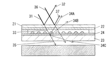
【解決手段】上基板21下面に上導電層22を形成し、下基板23上面に下導電層24を上導電層22と所定の空隙を設けて対向させて形成すると共に、下基板23上面には十点平均粗さRzが0.46μm以上で、かつ平均間隔Smが120.3μm以下の凹凸を設けたタッチパネルとして構成することにより、ニュートンリングとぎらつきの双方が抑制され、簡便な構成で視認性の良いタッチパネルを得ることができる。
【選択図】図1
Description
図1は本発明の一実施の形態によるタッチパネルの断面図であり、同図において、光透過性の上基板21の下面に光透過性かつ導電性で略矩形状の上導電層22が、同様に光透過性の下基板23の上面に光透過性かつ導電性で略矩形状の下導電層24が、スパッタリング法や真空蒸着法などによりほぼ全面に設けられている。

21 上基板
22 上導電層
23 下基板
23A 凹凸
24 下導電層
25 ドットスペーサ
26 スペーサ
30、30A〜30I タッチパネル
31、36 入射光
32、37 反射光
33、35 透過光
34A〜34C 散乱光
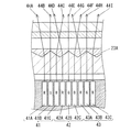
41、42、43 画素
41A、42A、43A 赤色ドット
41B、42B、43B 緑色ドット
41C、42C、43C 青色ドット
44A〜44I 光線
Claims (1)
- 上基板の下面に上導電層を形成し、下基板の上面に下導電層を上導電層と所定の空隙を設けて対向させて形成すると共に、上基板の下面または下基板の上面の少なくともいずれかに十点平均粗さRzが0.46μm以上で、かつ平均間隔Smが120.3μm以下の凹凸を設けたタッチパネル。
Priority Applications (1)
| Application Number | Priority Date | Filing Date | Title |
|---|---|---|---|
| JP2010204163A JP2012059191A (ja) | 2010-09-13 | 2010-09-13 | タッチパネル |
Applications Claiming Priority (1)
| Application Number | Priority Date | Filing Date | Title |
|---|---|---|---|
| JP2010204163A JP2012059191A (ja) | 2010-09-13 | 2010-09-13 | タッチパネル |
Publications (2)
| Publication Number | Publication Date |
|---|---|
| JP2012059191A true JP2012059191A (ja) | 2012-03-22 |
| JP2012059191A5 JP2012059191A5 (ja) | 2013-10-17 |
Family
ID=46056175
Family Applications (1)
| Application Number | Title | Priority Date | Filing Date |
|---|---|---|---|
| JP2010204163A Pending JP2012059191A (ja) | 2010-09-13 | 2010-09-13 | タッチパネル |
Country Status (1)
| Country | Link |
|---|---|
| JP (1) | JP2012059191A (ja) |
Cited By (2)
| Publication number | Priority date | Publication date | Assignee | Title |
|---|---|---|---|---|
| WO2014188918A1 (ja) * | 2013-05-24 | 2014-11-27 | 富士フイルム株式会社 | 透明導電膜及び透明導電膜の製造方法 |
| JP2015032071A (ja) * | 2013-07-31 | 2015-02-16 | 王子ホールディングス株式会社 | 導電性シートの製造方法、導電性シート、および、タッチパネル |
Citations (3)
| Publication number | Priority date | Publication date | Assignee | Title |
|---|---|---|---|---|
| JP2001324707A (ja) * | 2000-05-15 | 2001-11-22 | Gunze Ltd | 液晶デイスプレイ用タッチパネル |
| JP2007103348A (ja) * | 2005-09-12 | 2007-04-19 | Nitto Denko Corp | 透明導電性フィルム、タッチパネル用電極板およびタッチパネル |
| JP2009231183A (ja) * | 2008-03-25 | 2009-10-08 | Epson Imaging Devices Corp | タッチパネル、入力機能付き表示装置、および電子機器 |
-
2010
- 2010-09-13 JP JP2010204163A patent/JP2012059191A/ja active Pending
Patent Citations (3)
| Publication number | Priority date | Publication date | Assignee | Title |
|---|---|---|---|---|
| JP2001324707A (ja) * | 2000-05-15 | 2001-11-22 | Gunze Ltd | 液晶デイスプレイ用タッチパネル |
| JP2007103348A (ja) * | 2005-09-12 | 2007-04-19 | Nitto Denko Corp | 透明導電性フィルム、タッチパネル用電極板およびタッチパネル |
| JP2009231183A (ja) * | 2008-03-25 | 2009-10-08 | Epson Imaging Devices Corp | タッチパネル、入力機能付き表示装置、および電子機器 |
Cited By (4)
| Publication number | Priority date | Publication date | Assignee | Title |
|---|---|---|---|---|
| WO2014188918A1 (ja) * | 2013-05-24 | 2014-11-27 | 富士フイルム株式会社 | 透明導電膜及び透明導電膜の製造方法 |
| US9820380B2 (en) | 2013-05-24 | 2017-11-14 | Fujifilm Corporation | Transparent conductive film and method for producing transparent conductive film |
| US9820377B2 (en) | 2013-05-24 | 2017-11-14 | Fujifilm Corporation | Methods for producing a transparent conductive film for a touch panel |
| JP2015032071A (ja) * | 2013-07-31 | 2015-02-16 | 王子ホールディングス株式会社 | 導電性シートの製造方法、導電性シート、および、タッチパネル |
Similar Documents
| Publication | Publication Date | Title |
|---|---|---|
| CN110853507B (zh) | 一种显示屏和电子设备 | |
| CN110323354B (zh) | 显示面板及显示装置 | |
| JP4450089B2 (ja) | タッチパネル及び電気光学装置 | |
| JP4687561B2 (ja) | タッチパネル | |
| US9419612B2 (en) | Touch panel | |
| JP2003059641A (ja) | エレクトロルミネセント素子 | |
| JP2008027016A (ja) | タッチパネル | |
| CN104241541A (zh) | 有机电致发光器件及显示装置 | |
| CN113994253A (zh) | 显示装置及其制造方法 | |
| JP2006259815A (ja) | タッチパネル | |
| JP2012059191A (ja) | タッチパネル | |
| JP2017157467A (ja) | 面光源装置、表示装置、及び電子機器 | |
| TW201704951A (zh) | 觸控面板 | |
| CN115047668B (zh) | 显示面板及包括该显示面板的显示装置 | |
| JP2013214364A (ja) | 面状発光装置およびその製造方法 | |
| JP2016162454A (ja) | タッチパネル | |
| KR20110134174A (ko) | 유기 발광 다이오드 | |
| US8054392B2 (en) | Transparent composite material having ridge portion formed in transparent resistance film for transparent coordinate input device | |
| WO2021164581A1 (zh) | 显示基板及其制作方法、显示装置 | |
| JP4487757B2 (ja) | タッチパネル | |
| JP2004234386A (ja) | タッチパネル | |
| JP2007086959A (ja) | タッチパネル | |
| JP7122661B2 (ja) | タッチパネル | |
| JP2009271709A (ja) | タッチパネル | |
| JP2010170447A (ja) | 入力機能付表示装置、および電子機器 |
Legal Events
| Date | Code | Title | Description |
|---|---|---|---|
| A521 | Written amendment |
Free format text: JAPANESE INTERMEDIATE CODE: A523 Effective date: 20130830 |
|
| A621 | Written request for application examination |
Free format text: JAPANESE INTERMEDIATE CODE: A621 Effective date: 20130830 |
|
| RD01 | Notification of change of attorney |
Free format text: JAPANESE INTERMEDIATE CODE: A7421 Effective date: 20130912 |
|
| RD01 | Notification of change of attorney |
Free format text: JAPANESE INTERMEDIATE CODE: A7421 Effective date: 20140108 |
|
| A977 | Report on retrieval |
Free format text: JAPANESE INTERMEDIATE CODE: A971007 Effective date: 20140220 |
|
| A131 | Notification of reasons for refusal |
Free format text: JAPANESE INTERMEDIATE CODE: A131 Effective date: 20140311 |
|
| RD01 | Notification of change of attorney |
Free format text: JAPANESE INTERMEDIATE CODE: A7421 Effective date: 20140417 |
|
| A02 | Decision of refusal |
Free format text: JAPANESE INTERMEDIATE CODE: A02 Effective date: 20140701 |