JP2012059191A - Touch panel - Google Patents
Touch panel Download PDFInfo
- Publication number
- JP2012059191A JP2012059191A JP2010204163A JP2010204163A JP2012059191A JP 2012059191 A JP2012059191 A JP 2012059191A JP 2010204163 A JP2010204163 A JP 2010204163A JP 2010204163 A JP2010204163 A JP 2010204163A JP 2012059191 A JP2012059191 A JP 2012059191A
- Authority
- JP
- Japan
- Prior art keywords
- touch panel
- conductive layer
- light
- substrate
- unevenness
- Prior art date
- Legal status (The legal status is an assumption and is not a legal conclusion. Google has not performed a legal analysis and makes no representation as to the accuracy of the status listed.)
- Pending
Links
Images


Abstract
Description
本発明は、主に各種電子機器の操作に用いられるタッチパネルに関するものである。 The present invention relates to a touch panel used mainly for operating various electronic devices.
近年、携帯電話や電子カメラ等の各種電子機器の高機能化や多様化が進むに伴い、液晶ディスプレイの上面に光透過性のタッチパネルを装着し、このタッチパネルを通して下面の液晶ディスプレイの表示を見ながら、指やペン等でタッチパネルを押圧操作することによって、機器の様々な機能の切換えを行うものが増えており、視認性が良好なものが求められている。 In recent years, as various electronic devices such as mobile phones and electronic cameras have become highly functional and diversified, a light-transmissive touch panel is mounted on the upper surface of the liquid crystal display, and the display on the lower surface of the liquid crystal display is viewed through this touch panel. The number of devices that switch various functions of a device by pressing the touch panel with a finger, a pen, or the like is increasing, and a device with good visibility is required.
このような従来のタッチパネルについて、図5を用いて説明する。 Such a conventional touch panel will be described with reference to FIG.
なお、この図面は構成を判り易くするために、部分的に寸法を拡大して表している。 In addition, in this drawing, in order to make the configuration easy to understand, the dimensions are partially enlarged.
図5は従来のタッチパネルの断面図であり、同図において、光透過性の上基板1の下面に光透過性かつ導電性で略矩形状の上導電層2が、同様に光透過性の下基板3の上面に光透過性かつ導電性で略矩形状の下導電層4が、ほぼ全面に設けられている。
FIG. 5 is a cross-sectional view of a conventional touch panel, in which a light-transmitting and conductive upper rectangular
そして、上基板1の上面には数μmの高さの凹凸1Aが全面に渡って設けられている。
An upper surface of the upper substrate 1 is provided with
さらに、下導電層4の上面には絶縁樹脂によって、複数のドットスペーサ5が所定間隔で形成されると共に、上導電層2の両端には一対の上電極(図示せず)が、下導電層4の両端には、上電極とは直交方向の一対の下電極(図示せず)が各々形成されている。
Further, a plurality of
また、上基板1と下基板3間の外周内縁には、略額縁状のスペーサ6が形成され、このスペーサ6の上下面または片面に塗布形成された接着剤(図示せず)によって、上基板1と下基板3の外周が貼り合わされ、上導電層2と下導電層4が所定の空隙を空けて対向するようにして、タッチパネル10が構成されている。
Also, a substantially frame-like spacer 6 is formed on the inner peripheral edge between the upper substrate 1 and the
そして、このように構成されたタッチパネル10は、液晶ディスプレイ11の上方に配置されて電子機器に装着されると共に、一対の上電極と下電極が機器のマイコン等の制御回路(図示せず)に電気的に接続される。
The
以上の構成において、タッチパネル10背面の液晶ディスプレイ11の表示に応じて、上基板1上面を指やペン等で押圧操作すると、上基板1が撓み、押圧された箇所の上導電層2が下導電層4に接触する。
In the above configuration, when the upper surface of the upper substrate 1 is pressed with a finger or a pen according to the display on the
そして、制御回路から上電極と下電極へ順次電圧が印加され、これらの電極間の電圧比によって、押圧された箇所を制御回路が検出し、機器の様々な機能の切換えが行なわれる。 Then, a voltage is sequentially applied from the control circuit to the upper electrode and the lower electrode, and the control circuit detects the pressed position by the voltage ratio between these electrodes, and various functions of the device are switched.
このタッチパネル10は視認性を向上するため、ニュートンリングの発生を抑制している。ニュートンリングとは、上基板1や下基板3の上下面の様々な場所で反射した光が使用者の視認方向に対して、強めあいあるいは弱めあうことにより、タッチパネル10の表面が縞状に視認される現象である。
This
ここで、上基板1上面に凹凸1Aが設けられていることにより、上基板1や下基板3の上下面の様々な場所で反射した光が凹凸1Aで散乱されることで、ニュートンリングの発生を抑制するものであった。
Here, since the
なお、この出願の発明に関連する先行技術文献情報としては、例えば、特許文献1が知られている。 As prior art document information related to the invention of this application, for example, Patent Document 1 is known.
しかしながら、上記従来のタッチパネルにおいては、液晶ディスプレイ11の発光が凹凸1Aのレンズ効果により、タッチパネル10の表面がぎらついて視認される、いわゆる、ぎらつきという現象を生じ視認性が劣化するという課題があった。
However, the above-described conventional touch panel has a problem in that the light emission of the
なお、レンズ効果とは凹凸1Aの凸部を通過した光線は拡散し、凹部を通過した光線は集中する効果であり、これにより凹凸1Aを通過する光線の粗密が生じ、タッチパネル10の表面がぎらついて視認されるものである。
The lens effect is an effect in which light rays that have passed through the convex portions of the concave and
本発明は、このような従来の課題を解決するものであり、簡便な構成でニュートンリングとぎらつきの発生を抑え、視認性の良いタッチパネルを提供することを目的とする。 SUMMARY OF THE INVENTION The present invention solves such a conventional problem, and an object of the present invention is to provide a touch panel with good visibility by suppressing generation of Newton rings and glare with a simple configuration.
上記目的を達成するために本発明は、上基板の下面に上導電層を形成し、下基板の上面に下導電層を上導電層と所定の空隙を設けて対向させて形成すると共に、上基板の下面または下基板の上面のいずれかに十点平均粗さRzが0.46μm以上で、かつ平均間隔Smが120.3μm以下の凹凸を設けたタッチパネルとして構成することにより、ニュートンリングとぎらつきの双方が抑制され、簡便な構成で視認性の良いタッチパネルを得ることができるという作用を有するものである。 In order to achieve the above object, the present invention forms an upper conductive layer on the lower surface of the upper substrate, and forms the lower conductive layer on the upper surface of the lower substrate so as to face the upper conductive layer with a predetermined gap. By configuring as a touch panel having a ten-point average roughness Rz of 0.46 μm or more and an average interval Sm of 120.3 μm or less on either the lower surface of the substrate or the upper surface of the lower substrate, Newton rings and glare Both touches are suppressed, and a touch panel with good visibility can be obtained with a simple configuration.
以上のように本発明によれば、簡便な構成でニュートンリングとぎらつきの発生を抑え、視認性の良いタッチパネルを実現することができるという有利な効果が得られる。 As described above, according to the present invention, it is possible to obtain an advantageous effect that a Newton ring and glare can be suppressed with a simple configuration and a touch panel with high visibility can be realized.
以下、本発明の実施の形態について、図1〜図4を用いて説明する。 Hereinafter, embodiments of the present invention will be described with reference to FIGS.
なお、これらの図面は構成を判り易くするために、部分的に寸法を拡大して表している。 These drawings are partially enlarged in size for easy understanding of the configuration.
(実施の形態)
図1は本発明の一実施の形態によるタッチパネルの断面図であり、同図において、光透過性の上基板21の下面に光透過性かつ導電性で略矩形状の上導電層22が、同様に光透過性の下基板23の上面に光透過性かつ導電性で略矩形状の下導電層24が、スパッタリング法や真空蒸着法などによりほぼ全面に設けられている。
(Embodiment)
FIG. 1 is a cross-sectional view of a touch panel according to an embodiment of the present invention. In FIG. 1, a light-transmissive and conductive upper rectangular
ここで、上基板21と下基板23は、ガラスやポリエチレンテレフタレートやポリエーテルサルホン、ポリカーボネート等の光透過性のフィルム、アクリル等の光透過性の樹脂板で形成されている。
Here, the
また、下基板23は、あらかじめ上面の全面に、エッチング加工などにより凹凸23Aが設けられている。
Further, the
さらに、上導電層22や下導電層24は酸化インジウム錫や酸化錫等の光透過性で導電性の材料で形成されている。
Further, the upper
そして、下導電層24の上面にはエポキシやシリコーン等の絶縁樹脂によって複数のドットスペーサ25が所定間隔で形成されると共に、上導電層22の両端には一対の銀やカーボン等の上電極(図示せず)が、下導電層24の両端には、上電極とは直交方向の一対の銀やカーボン等の下電極(図示せず)が各々形成されている。
A plurality of
また、上基板21と下基板23間の外周内縁には、略額縁状のスペーサ26が形成され、このスペーサ26の上下面または片面に塗布形成された接着剤(図示せず)によって、上基板21と下基板23の外周が貼り合わされ、上導電層22と下導電層24が所定の空隙を空けて対向するようにして、タッチパネル30が構成されている。
Also, a substantially frame-
そして、このように構成されたタッチパネル30は、液晶ディスプレイ11の上方に配置されて電子機器に装着されると共に、一対の上電極と下電極が機器のマイコン等の制御回路(図示せず)に電気的に接続される。
The
以上の構成において、タッチパネル30背面の液晶ディスプレイ11の表示に応じて、上基板21上面を指やペン等で押圧操作すると、上基板21が撓み、押圧された箇所の上導電層22が下導電層24に接触する。
In the above configuration, when the upper surface of the
そして、制御回路から上電極と下電極へ順次電圧が印加され、これらの電極間の電圧比によって、押圧された箇所を制御回路が検出し、機器の様々な機能の切換えが行なわれる。 Then, a voltage is sequentially applied from the control circuit to the upper electrode and the lower electrode, and the control circuit detects the pressed position by the voltage ratio between these electrodes, and various functions of the device are switched.
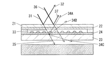
次に、タッチパネル30が、ニュートンリングとぎらつきの発生を抑制する原理について図2、図3のタッチパネルの光の経路を示す概念図、および図4の凹凸の評価指標を説明する図を用いて説明する。
Next, the principle that the
まず、図2を用いてニュートンリングの発生を抑制する原理について説明すると、同図において外光による入射光31の一部が上基板21の上面で反射し反射光32となり、残部が上基板21を透過する透過光33となる。
First, the principle of suppressing the occurrence of Newton rings will be described with reference to FIG. 2. In FIG. 2, a part of
そして透過光33は、上導電層22の上下面や下導電層24の上面でも一部が反射光(図示せず)として反射するが、残部が下基板23の上面に入射し、下基板23の上面で散乱光34A〜34Cなどとして散乱し、残部が下基板24内を透過する透過光35となる。
The transmitted light 33 is partially reflected as reflected light (not shown) on the upper and lower surfaces of the upper
ここで、タッチパネル30の操作者が視認する方向へ散乱した散乱光34Aは上基板21の上面を経由してタッチパネル30の外部へ放出される。この散乱光34Aが放出される上基板21の上面では、外光による入射光36の一部が反射光37として反射され、散乱光34Aと干渉してニュートンリングが発生する原因となるものであるが、上述のように、下基板23の上面の凹凸23Aで散乱光34A〜34Cなどとして散乱しているため、凹凸23Aが無い場合の反射光(図示せず)と比較すると、強度が弱くなる。つまり、凹凸23Aの存在により、ニュートンリングの発生が抑制されるものである。
Here, the scattered light 34 </ b> A scattered in the direction visually recognized by the operator of the
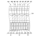
次に、図3を用いてぎらつきの発生を抑制する原理について説明すると、同図において、液晶ディスプレイ11の表示面は画素41、42、43などの複数の画素が発光するもので、画素41、42、43はそれぞれ赤色ドット41A、42A、43A、緑色ドット41B、42B、43B、青色ドット41C、42C、43Cから構成されている。それぞれのドットから発する光線44A〜44Iにおいて、凹凸23Aの右上方に傾いた面に入射した光線44A、44D、44Gは若干左に、左上方に傾いた面に入射した光線44C、44F、44Iは若干右に屈折する。そして、凹凸23Aの山の頂点を経由する光線44B、44E、44Hは直進する。ここで、凹凸23Aは狭ピッチで設けられているため、光線44A〜44Iのような隣り合うドットから発光した光線の進行方向に粗密を生じないので、ぎらつきの発生を抑制しうるものとなっている。
Next, the principle of suppressing the occurrence of glare will be described with reference to FIG. 3. In FIG. 3, the display surface of the
そして、このようなニュートンリングとぎらつきの抑制度合いは、凹凸23Aの表面粗さによって効果は異なる。一般に凹凸23Aの表面粗さを評価する評価指標として1994年のJIS B0601に規定される十点平均粗さRzと、平均間隔Smがあり、それぞれについて図4を用いて説明する。
And the effect of such a Newton ring and the suppression degree of a glare changes with surface roughness of the unevenness |
まず同図(a)は、十点平均粗さRzを説明するための図である。表面粗さを評価する対象物表面の凹凸を粗さ曲線といい、凹凸23Aの形状がこれに対応する。同図(a)の粗さ曲線において十点平均粗さRzとは、粗さ曲線から、その平均線の方向に基準長さLだけ抜き取り、この抜き取り部分の平均線から、最も高い山頂から5番目までの山頂の標高(Yp)の絶対値の平均値と、最も低い谷底から5番目までの谷底の標高(Yv)の絶対値の平均値との和であり(数1)で示される。
First, FIG. 6A is a diagram for explaining the ten-point average roughness Rz. The unevenness on the surface of the object for evaluating the surface roughness is called a roughness curve, and the shape of the

この十点平均粗さRzが大きくなるほど、凹凸23Aで反射光などが散乱しやすくなり、ニュートンリングが生じ難くなる。
As the ten-point average roughness Rz increases, reflected light and the like are more likely to be scattered by the
次に、同図(b)は、平均間隔Smを説明するための図である。同図(b)の粗さ曲線において平均間隔Smとは、粗さ曲線からその平均線の方向に基準長さLだけ抜き取り、1つの山およびそれに隣り合う1つの谷に対応する平均線の長さの和を求め、平均値で表したもので、(数2)で示される。 Next, FIG. 4B is a diagram for explaining the average interval Sm. In the roughness curve of FIG. 4B, the average interval Sm is the length of the average line corresponding to one peak and one valley adjacent to the reference length L extracted from the roughness curve in the direction of the average line. The sum of the values is obtained and expressed as an average value, which is represented by (Equation 2).
この平均間隔Smが小さくなるほど、液晶ディスプレイ11からの発光が凹凸23Aによりタッチパネル30から出力する方向の粗密が生じ難くなり、ぎらつきを抑制しうる。
As the average interval Sm becomes smaller, light emission from the
そして、凹凸23Aの形状が異なるタッチパネル30について、それぞれタッチパネル30A〜30Iとして、十点平均粗さRzと平均間隔Smの適正値について評価した結果について次に説明する。
And about the
ここで、(表1)は、十点平均粗さRzが小さい順にタッチパネル30A〜30Iを並べ、ニュートンリングの抑制度の評価結果を示したものである。 Here, (Table 1) arranges the touch panels 30A to 30I in ascending order of the ten-point average roughness Rz, and shows the evaluation results of the degree of suppression of Newton rings.
このニュートンリングの抑制度の評価結果は、「○」、「△」、「×」の順でニュートンリングの抑制効果は下がるもので、「△」まではニュートンリングの抑制効果があらわれたものである。ここで(表1)に示すようにRzが0.46μm以上であればニュートンリングを抑制しうる。 The evaluation result of the degree of inhibition of Newton's ring shows that the effect of inhibiting Newton's ring decreases in the order of “○”, “△”, and “×”. is there. Here, as shown in (Table 1), if Rz is 0.46 μm or more, Newton's ring can be suppressed.
また、(表2)は、平均間隔Smが小さい順にタッチパネル30A〜30Iを並べ、ぎらつきの抑制度の評価結果を示したものである。 (Table 2) shows the evaluation results of the degree of suppression of glare by arranging the touch panels 30A to 30I in ascending order of the average interval Sm.
このぎらつきの抑制度の評価結果は、「◎」、「○」、「△」、「×」の順でぎらつきの抑制効果は下がるもので、「△」まではぎらつきの抑制効果があらわれたものである。ここで(表2)に示すようにSmが120.3μm以下であれば、ぎらつきを抑制しうる。 The evaluation result of the degree of suppression of glare shows that the effect of suppressing glare decreases in the order of “◎”, “○”, “△”, “×”, and the effect of suppressing glare appears until “△”. It is. Here, if Sm is 120.3 μm or less as shown in (Table 2), glare can be suppressed.
すなわち、ニュートンリングとぎらつきの双方を抑制するには、凹凸23Aの形状を十点平均粗さRzが0.46μm以上で、かつ平均間隔Smが120.3μm以下となるようにすれば良い。
That is, in order to suppress both Newton rings and glare, the shape of the
なお、上述の説明では、下基板23の上面に凹凸23Aを設けるものとして説明したが、上基板21の下面に凹凸を設けるものとしても本発明の実施は可能である。
In the above description, it has been described that the
また、上述の説明で下基板23にエッチング加工により凹凸23Aを設けるものとしたのは、例えば下基板23の上面に樹脂による膜を形成し、それに凹凸を設けた場合と比較し、下基板23に入射あるいは下基板23を通過する光が凹凸23A以外の部分で反射や散乱する量が減るため、ニュートンリングとぎらつきの双方を抑制する効果が高いためである。
In the above description, the concave and
このように本実施の形態によれば、上基板21下面に上導電層22を形成し、下基板23上面に下導電層24を上導電層22と所定の空隙を設けて対向させて形成すると共に、上基板21下面または下基板23上面の少なくともいずれかには十点平均粗さRzが0.46μm以上で、かつ平均間隔Smが120.3μm以下の凹凸を設けたタッチパネルとして構成することにより、ニュートンリングとぎらつきの双方が抑制され、簡便な構成で視認性の良いタッチパネルを得ることができるものである。
Thus, according to the present embodiment, the upper
本発明によるタッチパネルは、簡便な構成で視認性の良いタッチパネルを得ることができるという有利な効果を有し、主に各種電子機器の操作用として有用である。 The touch panel according to the present invention has an advantageous effect of being able to obtain a touch panel with a simple configuration and good visibility, and is mainly useful for operation of various electronic devices.
11 液晶ディスプレイ
21 上基板
22 上導電層
23 下基板
23A 凹凸
24 下導電層
25 ドットスペーサ
26 スペーサ
30、30A〜30I タッチパネル
31、36 入射光
32、37 反射光
33、35 透過光
34A〜34C 散乱光
41、42、43 画素
41A、42A、43A 赤色ドット
41B、42B、43B 緑色ドット
41C、42C、43C 青色ドット
44A〜44I 光線
11
Claims (1)
Priority Applications (1)
| Application Number | Priority Date | Filing Date | Title |
|---|---|---|---|
| JP2010204163A JP2012059191A (en) | 2010-09-13 | 2010-09-13 | Touch panel |
Applications Claiming Priority (1)
| Application Number | Priority Date | Filing Date | Title |
|---|---|---|---|
| JP2010204163A JP2012059191A (en) | 2010-09-13 | 2010-09-13 | Touch panel |
Publications (2)
| Publication Number | Publication Date |
|---|---|
| JP2012059191A true JP2012059191A (en) | 2012-03-22 |
| JP2012059191A5 JP2012059191A5 (en) | 2013-10-17 |
Family
ID=46056175
Family Applications (1)
| Application Number | Title | Priority Date | Filing Date |
|---|---|---|---|
| JP2010204163A Pending JP2012059191A (en) | 2010-09-13 | 2010-09-13 | Touch panel |
Country Status (1)
| Country | Link |
|---|---|
| JP (1) | JP2012059191A (en) |
Cited By (2)
| Publication number | Priority date | Publication date | Assignee | Title |
|---|---|---|---|---|
| WO2014188918A1 (en) * | 2013-05-24 | 2014-11-27 | 富士フイルム株式会社 | Transparent conductive film and method for producing transparent conductive film |
| JP2015032071A (en) * | 2013-07-31 | 2015-02-16 | 王子ホールディングス株式会社 | Method for manufacturing conductive sheet, conductive sheet and touch panel |
Citations (3)
| Publication number | Priority date | Publication date | Assignee | Title |
|---|---|---|---|---|
| JP2001324707A (en) * | 2000-05-15 | 2001-11-22 | Gunze Ltd | Touch panel for liquid crystal display |
| JP2007103348A (en) * | 2005-09-12 | 2007-04-19 | Nitto Denko Corp | Transparent conductive film, electrode plate for touch panel, and the touch panel |
| JP2009231183A (en) * | 2008-03-25 | 2009-10-08 | Epson Imaging Devices Corp | Tough panel, display device with input function, and electronic equipment |
-
2010
- 2010-09-13 JP JP2010204163A patent/JP2012059191A/en active Pending
Patent Citations (3)
| Publication number | Priority date | Publication date | Assignee | Title |
|---|---|---|---|---|
| JP2001324707A (en) * | 2000-05-15 | 2001-11-22 | Gunze Ltd | Touch panel for liquid crystal display |
| JP2007103348A (en) * | 2005-09-12 | 2007-04-19 | Nitto Denko Corp | Transparent conductive film, electrode plate for touch panel, and the touch panel |
| JP2009231183A (en) * | 2008-03-25 | 2009-10-08 | Epson Imaging Devices Corp | Tough panel, display device with input function, and electronic equipment |
Cited By (4)
| Publication number | Priority date | Publication date | Assignee | Title |
|---|---|---|---|---|
| WO2014188918A1 (en) * | 2013-05-24 | 2014-11-27 | 富士フイルム株式会社 | Transparent conductive film and method for producing transparent conductive film |
| US9820377B2 (en) | 2013-05-24 | 2017-11-14 | Fujifilm Corporation | Methods for producing a transparent conductive film for a touch panel |
| US9820380B2 (en) | 2013-05-24 | 2017-11-14 | Fujifilm Corporation | Transparent conductive film and method for producing transparent conductive film |
| JP2015032071A (en) * | 2013-07-31 | 2015-02-16 | 王子ホールディングス株式会社 | Method for manufacturing conductive sheet, conductive sheet and touch panel |
Similar Documents
| Publication | Publication Date | Title |
|---|---|---|
| CN110853507B (en) | Display screen and electronic equipment | |
| CN110323354B (en) | Display panel and display device | |
| JP4450089B2 (en) | Touch panel and electro-optical device | |
| JP4687561B2 (en) | Touch panel | |
| US9419612B2 (en) | Touch panel | |
| JP2008027016A (en) | Touch panel | |
| CN104241541A (en) | Organic electroluminescence device and display device | |
| CN113994253A (en) | Display device and method for manufacturing the same | |
| JP2006259815A (en) | Touch panel | |
| JP2012059191A (en) | Touch panel | |
| JP2017157467A (en) | Surface light source device, display device, and electronic equipment | |
| TW201704951A (en) | Touch panel | |
| CN115047668B (en) | Display panel and display device comprising same | |
| JP2013214364A (en) | Planar light-emitting device and method for manufacturing the same | |
| US20160132175A1 (en) | Optical film and touch controlled display apparatus using the same | |
| JP2016162454A (en) | Touch panel | |
| KR20110134174A (en) | Organic light emitting diode | |
| US8054392B2 (en) | Transparent composite material having ridge portion formed in transparent resistance film for transparent coordinate input device | |
| WO2021164581A1 (en) | Display substrate and manufacturing method therefor, and display device | |
| JP4487757B2 (en) | Touch panel | |
| WO2015118879A1 (en) | Touch panel | |
| JP2004234386A (en) | Touch panel | |
| JP2007086959A (en) | Touch panel | |
| JP7122661B2 (en) | touch panel | |
| JP2009271709A (en) | Touch panel |
Legal Events
| Date | Code | Title | Description |
|---|---|---|---|
| A521 | Written amendment |
Free format text: JAPANESE INTERMEDIATE CODE: A523 Effective date: 20130830 |
|
| A621 | Written request for application examination |
Free format text: JAPANESE INTERMEDIATE CODE: A621 Effective date: 20130830 |
|
| RD01 | Notification of change of attorney |
Free format text: JAPANESE INTERMEDIATE CODE: A7421 Effective date: 20130912 |
|
| RD01 | Notification of change of attorney |
Free format text: JAPANESE INTERMEDIATE CODE: A7421 Effective date: 20140108 |
|
| A977 | Report on retrieval |
Free format text: JAPANESE INTERMEDIATE CODE: A971007 Effective date: 20140220 |
|
| A131 | Notification of reasons for refusal |
Free format text: JAPANESE INTERMEDIATE CODE: A131 Effective date: 20140311 |
|
| RD01 | Notification of change of attorney |
Free format text: JAPANESE INTERMEDIATE CODE: A7421 Effective date: 20140417 |
|
| A02 | Decision of refusal |
Free format text: JAPANESE INTERMEDIATE CODE: A02 Effective date: 20140701 |