WO2014142183A1 - Substrat à matrice active, procédé de fabrication de substrat à matrice active et panneau d'affichage - Google Patents
Substrat à matrice active, procédé de fabrication de substrat à matrice active et panneau d'affichage Download PDFInfo
- Publication number
- WO2014142183A1 WO2014142183A1 PCT/JP2014/056527 JP2014056527W WO2014142183A1 WO 2014142183 A1 WO2014142183 A1 WO 2014142183A1 JP 2014056527 W JP2014056527 W JP 2014056527W WO 2014142183 A1 WO2014142183 A1 WO 2014142183A1
- Authority
- WO
- WIPO (PCT)
- Prior art keywords
- gate
- active matrix
- gate line
- matrix substrate
- region
- Prior art date
Links
Images


Classifications
-
- G—PHYSICS
- G09—EDUCATION; CRYPTOGRAPHY; DISPLAY; ADVERTISING; SEALS
- G09G—ARRANGEMENTS OR CIRCUITS FOR CONTROL OF INDICATING DEVICES USING STATIC MEANS TO PRESENT VARIABLE INFORMATION
- G09G3/00—Control arrangements or circuits, of interest only in connection with visual indicators other than cathode-ray tubes
- G09G3/20—Control arrangements or circuits, of interest only in connection with visual indicators other than cathode-ray tubes for presentation of an assembly of a number of characters, e.g. a page, by composing the assembly by combination of individual elements arranged in a matrix no fixed position being assigned to or needed to be assigned to the individual characters or partial characters
- G09G3/34—Control arrangements or circuits, of interest only in connection with visual indicators other than cathode-ray tubes for presentation of an assembly of a number of characters, e.g. a page, by composing the assembly by combination of individual elements arranged in a matrix no fixed position being assigned to or needed to be assigned to the individual characters or partial characters by control of light from an independent source
- G09G3/36—Control arrangements or circuits, of interest only in connection with visual indicators other than cathode-ray tubes for presentation of an assembly of a number of characters, e.g. a page, by composing the assembly by combination of individual elements arranged in a matrix no fixed position being assigned to or needed to be assigned to the individual characters or partial characters by control of light from an independent source using liquid crystals
- G09G3/3611—Control of matrices with row and column drivers
- G09G3/3648—Control of matrices with row and column drivers using an active matrix
- G09G3/3666—Control of matrices with row and column drivers using an active matrix with the matrix divided into sections
-
- G—PHYSICS
- G02—OPTICS
- G02F—OPTICAL DEVICES OR ARRANGEMENTS FOR THE CONTROL OF LIGHT BY MODIFICATION OF THE OPTICAL PROPERTIES OF THE MEDIA OF THE ELEMENTS INVOLVED THEREIN; NON-LINEAR OPTICS; FREQUENCY-CHANGING OF LIGHT; OPTICAL LOGIC ELEMENTS; OPTICAL ANALOGUE/DIGITAL CONVERTERS
- G02F1/00—Devices or arrangements for the control of the intensity, colour, phase, polarisation or direction of light arriving from an independent light source, e.g. switching, gating or modulating; Non-linear optics
- G02F1/01—Devices or arrangements for the control of the intensity, colour, phase, polarisation or direction of light arriving from an independent light source, e.g. switching, gating or modulating; Non-linear optics for the control of the intensity, phase, polarisation or colour
- G02F1/13—Devices or arrangements for the control of the intensity, colour, phase, polarisation or direction of light arriving from an independent light source, e.g. switching, gating or modulating; Non-linear optics for the control of the intensity, phase, polarisation or colour based on liquid crystals, e.g. single liquid crystal display cells
- G02F1/133—Constructional arrangements; Operation of liquid crystal cells; Circuit arrangements
- G02F1/1333—Constructional arrangements; Manufacturing methods
- G02F1/1345—Conductors connecting electrodes to cell terminals
-
- G—PHYSICS
- G09—EDUCATION; CRYPTOGRAPHY; DISPLAY; ADVERTISING; SEALS
- G09G—ARRANGEMENTS OR CIRCUITS FOR CONTROL OF INDICATING DEVICES USING STATIC MEANS TO PRESENT VARIABLE INFORMATION
- G09G3/00—Control arrangements or circuits, of interest only in connection with visual indicators other than cathode-ray tubes
- G09G3/20—Control arrangements or circuits, of interest only in connection with visual indicators other than cathode-ray tubes for presentation of an assembly of a number of characters, e.g. a page, by composing the assembly by combination of individual elements arranged in a matrix no fixed position being assigned to or needed to be assigned to the individual characters or partial characters
- G09G3/34—Control arrangements or circuits, of interest only in connection with visual indicators other than cathode-ray tubes for presentation of an assembly of a number of characters, e.g. a page, by composing the assembly by combination of individual elements arranged in a matrix no fixed position being assigned to or needed to be assigned to the individual characters or partial characters by control of light from an independent source
- G09G3/36—Control arrangements or circuits, of interest only in connection with visual indicators other than cathode-ray tubes for presentation of an assembly of a number of characters, e.g. a page, by composing the assembly by combination of individual elements arranged in a matrix no fixed position being assigned to or needed to be assigned to the individual characters or partial characters by control of light from an independent source using liquid crystals
- G09G3/3611—Control of matrices with row and column drivers
- G09G3/3648—Control of matrices with row and column drivers using an active matrix
-
- G—PHYSICS
- G09—EDUCATION; CRYPTOGRAPHY; DISPLAY; ADVERTISING; SEALS
- G09G—ARRANGEMENTS OR CIRCUITS FOR CONTROL OF INDICATING DEVICES USING STATIC MEANS TO PRESENT VARIABLE INFORMATION
- G09G3/00—Control arrangements or circuits, of interest only in connection with visual indicators other than cathode-ray tubes
- G09G3/20—Control arrangements or circuits, of interest only in connection with visual indicators other than cathode-ray tubes for presentation of an assembly of a number of characters, e.g. a page, by composing the assembly by combination of individual elements arranged in a matrix no fixed position being assigned to or needed to be assigned to the individual characters or partial characters
- G09G3/34—Control arrangements or circuits, of interest only in connection with visual indicators other than cathode-ray tubes for presentation of an assembly of a number of characters, e.g. a page, by composing the assembly by combination of individual elements arranged in a matrix no fixed position being assigned to or needed to be assigned to the individual characters or partial characters by control of light from an independent source
- G09G3/36—Control arrangements or circuits, of interest only in connection with visual indicators other than cathode-ray tubes for presentation of an assembly of a number of characters, e.g. a page, by composing the assembly by combination of individual elements arranged in a matrix no fixed position being assigned to or needed to be assigned to the individual characters or partial characters by control of light from an independent source using liquid crystals
- G09G3/3611—Control of matrices with row and column drivers
- G09G3/3674—Details of drivers for scan electrodes
- G09G3/3677—Details of drivers for scan electrodes suitable for active matrices only
-
- G—PHYSICS
- G02—OPTICS
- G02F—OPTICAL DEVICES OR ARRANGEMENTS FOR THE CONTROL OF LIGHT BY MODIFICATION OF THE OPTICAL PROPERTIES OF THE MEDIA OF THE ELEMENTS INVOLVED THEREIN; NON-LINEAR OPTICS; FREQUENCY-CHANGING OF LIGHT; OPTICAL LOGIC ELEMENTS; OPTICAL ANALOGUE/DIGITAL CONVERTERS
- G02F1/00—Devices or arrangements for the control of the intensity, colour, phase, polarisation or direction of light arriving from an independent light source, e.g. switching, gating or modulating; Non-linear optics
- G02F1/01—Devices or arrangements for the control of the intensity, colour, phase, polarisation or direction of light arriving from an independent light source, e.g. switching, gating or modulating; Non-linear optics for the control of the intensity, phase, polarisation or colour
- G02F1/13—Devices or arrangements for the control of the intensity, colour, phase, polarisation or direction of light arriving from an independent light source, e.g. switching, gating or modulating; Non-linear optics for the control of the intensity, phase, polarisation or colour based on liquid crystals, e.g. single liquid crystal display cells
- G02F1/133—Constructional arrangements; Operation of liquid crystal cells; Circuit arrangements
- G02F1/1333—Constructional arrangements; Manufacturing methods
- G02F1/1345—Conductors connecting electrodes to cell terminals
- G02F1/13456—Cell terminals located on one side of the display only
-
- G—PHYSICS
- G02—OPTICS
- G02F—OPTICAL DEVICES OR ARRANGEMENTS FOR THE CONTROL OF LIGHT BY MODIFICATION OF THE OPTICAL PROPERTIES OF THE MEDIA OF THE ELEMENTS INVOLVED THEREIN; NON-LINEAR OPTICS; FREQUENCY-CHANGING OF LIGHT; OPTICAL LOGIC ELEMENTS; OPTICAL ANALOGUE/DIGITAL CONVERTERS
- G02F2201/00—Constructional arrangements not provided for in groups G02F1/00 - G02F7/00
- G02F2201/56—Substrates having a particular shape, e.g. non-rectangular
-
- G—PHYSICS
- G09—EDUCATION; CRYPTOGRAPHY; DISPLAY; ADVERTISING; SEALS
- G09G—ARRANGEMENTS OR CIRCUITS FOR CONTROL OF INDICATING DEVICES USING STATIC MEANS TO PRESENT VARIABLE INFORMATION
- G09G2300/00—Aspects of the constitution of display devices
- G09G2300/04—Structural and physical details of display devices
- G09G2300/0421—Structural details of the set of electrodes
- G09G2300/0426—Layout of electrodes and connections
-
- G—PHYSICS
- G09—EDUCATION; CRYPTOGRAPHY; DISPLAY; ADVERTISING; SEALS
- G09G—ARRANGEMENTS OR CIRCUITS FOR CONTROL OF INDICATING DEVICES USING STATIC MEANS TO PRESENT VARIABLE INFORMATION
- G09G2310/00—Command of the display device
- G09G2310/02—Addressing, scanning or driving the display screen or processing steps related thereto
- G09G2310/0202—Addressing of scan or signal lines
- G09G2310/0218—Addressing of scan or signal lines with collection of electrodes in groups for n-dimensional addressing
-
- G—PHYSICS
- G09—EDUCATION; CRYPTOGRAPHY; DISPLAY; ADVERTISING; SEALS
- G09G—ARRANGEMENTS OR CIRCUITS FOR CONTROL OF INDICATING DEVICES USING STATIC MEANS TO PRESENT VARIABLE INFORMATION
- G09G2310/00—Command of the display device
- G09G2310/02—Addressing, scanning or driving the display screen or processing steps related thereto
- G09G2310/0264—Details of driving circuits
- G09G2310/0278—Details of driving circuits arranged to drive both scan and data electrodes
-
- G—PHYSICS
- G09—EDUCATION; CRYPTOGRAPHY; DISPLAY; ADVERTISING; SEALS
- G09G—ARRANGEMENTS OR CIRCUITS FOR CONTROL OF INDICATING DEVICES USING STATIC MEANS TO PRESENT VARIABLE INFORMATION
- G09G2310/00—Command of the display device
- G09G2310/02—Addressing, scanning or driving the display screen or processing steps related thereto
- G09G2310/0264—Details of driving circuits
- G09G2310/0281—Arrangement of scan or data electrode driver circuits at the periphery of a panel not inherent to a split matrix structure
-
- G—PHYSICS
- G09—EDUCATION; CRYPTOGRAPHY; DISPLAY; ADVERTISING; SEALS
- G09G—ARRANGEMENTS OR CIRCUITS FOR CONTROL OF INDICATING DEVICES USING STATIC MEANS TO PRESENT VARIABLE INFORMATION
- G09G2310/00—Command of the display device
- G09G2310/02—Addressing, scanning or driving the display screen or processing steps related thereto
- G09G2310/0264—Details of driving circuits
- G09G2310/0291—Details of output amplifiers or buffers arranged for use in a driving circuit
-
- G—PHYSICS
- G09—EDUCATION; CRYPTOGRAPHY; DISPLAY; ADVERTISING; SEALS
- G09G—ARRANGEMENTS OR CIRCUITS FOR CONTROL OF INDICATING DEVICES USING STATIC MEANS TO PRESENT VARIABLE INFORMATION
- G09G2320/00—Control of display operating conditions
- G09G2320/02—Improving the quality of display appearance
- G09G2320/0233—Improving the luminance or brightness uniformity across the screen
-
- G—PHYSICS
- G09—EDUCATION; CRYPTOGRAPHY; DISPLAY; ADVERTISING; SEALS
- G09G—ARRANGEMENTS OR CIRCUITS FOR CONTROL OF INDICATING DEVICES USING STATIC MEANS TO PRESENT VARIABLE INFORMATION
- G09G2380/00—Specific applications
- G09G2380/16—Digital picture frames
Definitions
- the gate line driving unit disposed in at least a part of the outer peripheral portion of the display area is higher in driving frequency than other gate line driving units.
- the selection signal is output at the driving frequency.
- a display panel according to an eighteenth invention comprises an active matrix substrate according to any one of the first to twelfth inventions, a counter substrate comprising a color filter and a common electrode, the active matrix substrate, and the counter substrate. A liquid crystal layer sandwiched therebetween.
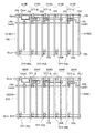
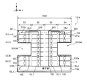
- FIG. 7A is a cross-sectional view of the TFT-PIX portion in FIG. 6 taken along line II.
- FIG. 7B is a cross-sectional view taken along line II-II of contact portion CH1 in FIG.
- FIG. 7C is a cross-sectional view of the TFT-A portion in FIG. 6 taken along the line III-III.
- FIG. 7D is a cross-sectional view of the contact portion CH2 in FIG. 6 cut along line IV-IV.
- FIG. 8A is an enlarged plan view of the pixel region 204R shown in FIG. 5B.
- FIG. 8B is an enlarged plan view of the pixel region 205R shown in FIG. 5B.
- FIG. 8C is an enlarged plan view of the pixel region 203G shown in FIG. 5A.
- FIG. 8D is an enlarged plan view of the pixel region 205B shown in FIG. 5C.
- FIG. 8E is an enlarged plan view of the pixel region 203B shown in FIG. 5B.
- FIG. 8F is an enlarged plan view of the pixel regions 201R and 201G shown in FIG. 5A.
- FIG. 9 is a timing chart when the gate driver shown in FIG. 4 scans the gate line.
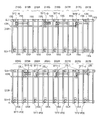
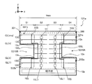
- FIG. 10 is a schematic configuration diagram of an active matrix substrate in the second embodiment.
- FIG. 11 is a diagram showing the drive timing of the active matrix substrate shown in FIG.
- FIG. 12A is a schematic configuration diagram of an active matrix substrate in the third embodiment.
- FIG. 18 is a schematic configuration diagram of an active matrix substrate in the sixth embodiment.
- FIG. 19 is a schematic configuration diagram of an active matrix substrate in the seventh embodiment.
- FIG. 20 is a diagram illustrating an example of an equivalent circuit of the gate driver in the seventh embodiment.
- FIG. 21A is a timing chart when the gate driver shown in FIG. 20 scans the gate line.
- FIG. 21B is a timing chart when the gate driver shown in FIG. 20 scans the gate line.
- FIG. 22A is a diagram illustrating an arrangement example of the gate drivers illustrated in FIG. 22B is a diagram illustrating an arrangement example of the gate drivers illustrated in FIG.
- FIG. 23A is a diagram showing an example of moving image data displayed on the active matrix substrate shown in FIG. FIG.
- FIG. 30C is a view for explaining a second manufacturing method in the ninth embodiment.
- FIG. 30D is a view for explaining a second manufacturing method in the ninth embodiment.
- FIG. 31A is a schematic configuration diagram of a first active matrix substrate of Application Example 1 in the ninth embodiment.
- FIG. 31B is a diagram in which the first active matrix substrate shown in FIG. 31A is cut.
- FIG. 31C is a schematic configuration diagram of a second active matrix substrate generated from one of the cut first active matrix substrates shown in FIG. 31B.
- FIG. 31D is a schematic configuration diagram of a second active matrix substrate generated from the other of the cut first active matrix substrates shown in FIG. 31B.
- FIG. 31E is a schematic configuration diagram when the first active matrix substrate shown in FIG. 31A is used for a display.
- FIG. 31A is a schematic configuration diagram of a first active matrix substrate of Application Example 1 in the ninth embodiment.
- FIG. 31B is a diagram in which the first active matrix substrate shown in FIG. 31A is
- FIG. 32 is a schematic configuration diagram of a first active matrix substrate according to Application Example 2 of the ninth embodiment.
- FIG. 33A is a schematic configuration diagram of a first active matrix substrate according to Application 3 of the ninth embodiment.
- FIG. 33B is a cross-sectional view of the first active matrix substrate shown in FIG. 33A.
- FIG. 34A is a schematic configuration diagram of a first active matrix substrate according to Application 1 of the ninth embodiment.
- FIG. 34B is a view of the first active matrix substrate shown in FIG. 34 cut.
- FIG. 35A is a schematic configuration diagram of an active matrix substrate in the first modification.
- FIG. 35B is a diagram illustrating another wiring example of the source line in the first modification.
- FIG. 36A is a schematic configuration diagram of an active matrix substrate in Modification 2.
- FIG. 36B is a diagram illustrating another wiring example of the source line in the second modification.
- a gate line group including a plurality of gate lines and a source line group including a plurality of source lines are arranged in a matrix, and the gate lines and the source lines are arranged in a matrix.
- a gate line driving unit that outputs a selection signal to be switched, and among the gate line groups, at least some of the gate line groups are larger than a maximum length of a width in a first direction in which the gate lines extend in the display region. Short (first Adult).
- the active matrix substrate includes a gate line group including a gate line having a length shorter than the maximum length in the first direction of the active matrix substrate, and a source line group intersecting the gate line.
- the active matrix substrate includes, for example, a substrate having a display area other than a rectangle, a substrate having a rectangular display area, and having gate lines divided.
- Each gate line is sequentially selected by a gate line driving unit formed in the display area in accordance with a control signal supplied from a second terminal unit provided on one side of the frame area.
- a data signal is supplied from a first terminal portion provided on the same side as the second terminal portion.
- a second configuration has a non-display region in the display region in the first configuration, and a part of the source lines in the source line group includes the first of the columns in which the non-display region is arranged.
- the end in the second direction extending from the first terminal portion is located in the vicinity of the end on the non-display region side in the first display region.
- a part of the source line group arranged in the column extends from the first terminal portion and extends to the second display region opposite to the first display region with respect to the non-display region. It is good as it is.
- the source line of the first display region in the column in which the non-display region is formed is formed from the first terminal portion to the end portion on the non-display region side of the first display region, and the second In the display region, source lines are formed by extending source lines of other columns. Therefore, the data signal can be supplied also to the display area of the column where the non-display area is formed.
- the first terminal has a non-display area in the display area, and the first terminal with respect to the non-display area among the display areas of the column where the non-display area is arranged.
- the source line arranged in the first display area on the part side extends from the first terminal part, and the extending end part in the second direction is the end on the non-display area side in the first display area.
- the source line connected via the detour wiring is formed in the first display area and the second display area of the column in which the non-display area is formed. Therefore, the data signal can be supplied also to the display area of the column in which the non-display area is formed.
- a fourth configuration includes a wiring group extending from the second terminal portion so as to be substantially parallel to the source line and connected to the gate line driving unit in the second configuration, and the pixels in the same row
- At least a part of the gate line connected to the electrode is composed of discontinuous partial gate lines, and the partial gate lines are connected to the different gate line driving units, and are part of the wiring group.
- the wiring extends from the second terminal portion in the first display region, and the end in the extending direction is located near the end on the non-display region side in the first display region, and is in another row.
- a part of the arranged wiring group may extend from the second terminal portion and extend to the second display area.
- the bypass wiring is formed in the pixel region where the gate line driving unit is not formed. Therefore, the difference in aperture ratio between the pixel region in which the gate line driver is formed and the pixel region in which the bypass wiring is formed can be reduced, and luminance unevenness can be reduced.
- the gate line driving unit arranged in at least a part of the outer peripheral portion of the display area outputs a selection signal at a driving frequency higher than the driving frequency of the other gate line driving units. Therefore, even when impurities in the sealing material for sealing the liquid crystal layer are mixed in the vicinity of the outer periphery of the display region, display unevenness due to the influence of the impurities in the sealing material can be reduced.
- the gate line can be brought into a non-selected state in at least a part of the frames. Therefore, for example, when displaying a still image, the gate line is switched to a selected state during some frames and the gate line is switched to a non-selected state during other frames. Power consumption when switching to can be reduced.
- the source line groups are shorter than other source line groups, and some of the gate line groups are columns in which some of the source line groups are arranged. Placed on a line that does not intersect In other words, since the number of gate lines in a region where another source line group is arranged is larger than a region where some source line groups are arranged, the region where some source line groups are arranged is different from other source lines.
- the period during which the gate line is switched to the selected state is shorter than the region where the group is arranged. During the period when some of the gate line groups are switched to the selected state, a data signal having a minimum amplitude is supplied to some of the source line groups. Electric power can be reduced.
- An active matrix substrate manufacturing method includes a step of generating a plurality of gate lines having substantially the same length and arranged at a predetermined interval, and the gate having the same length.
- a part of the first active matrix substrate is removed so that a part of the gate line is shorter than a maximum length of the width of the display region in a direction in which the gate line extends Te comprises a removal step for generating a second active matrix substrate, a (Configuration 13).
- the order of the steps in the forming step is not limited to this, and the order may be arbitrary.
- a display panel includes an active matrix substrate having any one of the first to twelfth configurations, a counter substrate including a color filter and a common electrode, the active matrix substrate, and the counter substrate. A liquid crystal layer sandwiched between them (eighteenth configuration).
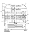
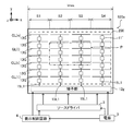
- a plurality of gate drivers 11 are connected to the gate lines 13G of GL (1) to GL (n) in the display area.
- the gate drivers 11 connected to the same gate line 13G are synchronized, and one gate line 13G is simultaneously driven by a set signal output from these gate drivers 11.
- each of the gate drivers 11 is connected to the gate lines 13G at substantially equal intervals so that the load for driving one gate line 13G is substantially equal.
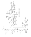
- a wiring in which the source terminal of TFT-B, the drain terminal of TFT-A, the source terminal of TFT-C, and the gate terminal of TFT-F are connected is referred to as netA.
- a wiring connecting the gate terminal of the TFT-C, the source terminal of the TFT-G, the drain terminal of the TFT-H, the source terminal of the TFT-I, and the source terminal of the TFT-J is denoted by netB. Called.
- the clock signals supplied to the TFT-D, TFT-F, TFT-H, and TFT-G are supplied to the TFTs of the gate drivers 11 in adjacent rows. They are arranged so as to be opposite in phase to the clock signals supplied to each. That is, TFT-D, TFT-F, TFT-H, and TFT-G are arranged in a pixel region that is shifted in the horizontal direction from the pixel region in which these TFTs in adjacent rows are formed.
- the TFT-G in the upper pixel region is formed in the pixel region 216G, while the TFT-G in the lower pixel region is formed in the pixel region 205B.
- the clock signal (CKA) is supplied to the TFT-D in the upper pixel area, and the clock signal (CKA) having a phase opposite to that of the clock signal (CKA) is supplied to the TFT-D in the lower pixel area.
- CKB is supplied.
- clock signals (CKA or CKB) having opposite phases are supplied to the upper pixel region and the lower pixel region.
- Drain terminal 15Sd 1 in the contact portion CH3, it is connected to the gate line 13G of GL (n-2), in the contact portion CH4, is connected to the gate terminal 13 g.
- the source terminal 15Sd 2 of B2 side is connected to the wiring 13N in the contact portion CH2.
- the TFT-B is connected to the netA and receives the set signal (S) via the gate line 13G of GL (n-2).
- the source wiring layer 15 forms a source-drain terminal 15sd (including 15sd 1 and 15sd 2 ) of the TFT-C and a wiring 15L1.
- drain terminal 15Sd 1 and the wiring 13Na of C1 side is connected.
- the TFT-C is connected to netA by a wiring 13Na and connected to netB by a wiring 13Nb.
- the TFT-C is supplied with a power supply voltage signal (VSS) via the wiring 15L1.
- VSS power supply voltage signal
- source terminal 15Sd 2 of G2 side of TFT-G are connected to the wiring 13N. Further, the gate terminal 13g of the TFT-G, in the contact portion CH4, is connected to the drain terminal 15Sd 1 and the wiring 15L1 of G1 side. Thereby, the TFT-G is connected to the netB, and the clock signal (CKB) is supplied through the wiring 15L1.
- the connection portion 15Lc has substantially the same width as the wiring 13N, is formed to extend from the electrode 15c to the contact portion CH2, and is connected to the wiring 13N at the contact portion CH2. Further, the wiring 15L2 is formed to extend from the end of the connection portion 15Lc on the contact portion CH2 side to the vicinity of the contact portion CH1. In the present embodiment, the wiring 15L2 is formed so that the aperture ratio of the pixel region where the capacitor Cbst is formed and the aperture ratio of other pixel regions are matched. In the contact portion CH2, the electrode 15c is connected to the wiring 13N by the connection portion 15Lc. Thereby, the capacitor Cbst is connected to netA.
- FIG. 8F is an enlarged plan view of the pixel regions 201B and 202R shown in FIG. 5A.
- the illustration of the light shielding region BM is omitted.
- the source terminal 15s and the drain terminal 15d of the TFT-D and the wiring 15L1 are formed by the source wiring layer 15 as in the pixel areas 204G and 204B described above.
- the drain terminal 15d is connected to the GL (n ⁇ 1) gate line 13G at the contact portion CH5 in the pixel region 201B.
- the TFT-D is supplied with the power supply voltage signal (VSS) and the clock signal (CKA) via the wiring 15L1 in the pixel regions 201B and 202R, and the timing at which the clock signal (CKA) becomes H level is set via the contact portion CH5.
- An L-level potential (VSS) is output to the gate line 13G of GL (n ⁇ 1).
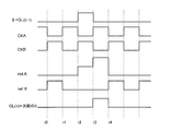
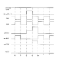
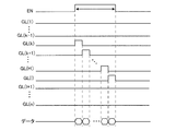
- FIG. 9 is a timing chart when the gate driver 11 scans the gate line 13G.
- a period from t3 to t4 is a period in which the GL (n) gate line 13G is selected.
- a clock signal (CKA) and a clock signal (CKB) supplied from the display control circuit 4 and whose phases are inverted every horizontal scanning period are input to the gate driver 11 via terminals 116 to 119.
- a reset signal (CLR) that is at a H (High) level for a certain period every vertical scanning period is sent from the display control circuit 4 to the gate driver 11 via the terminals 113 to 115. Entered.
- the reset signal (CLR) is input, the netA, netB, and gate line 13G transition to the L (Low) level.
- an L level clock signal (CKA) is input to the terminals 116 and 117, and an H level clock signal (CKB) is input to the terminals 118 and 119.
- CKA L level clock signal
- CKB H level clock signal
- TFT-G is turned on and TFT-H is turned off, so that netB is charged to the H level.
- TFT-C and TFT-D are turned on and TFT-F is turned off, netA is charged to the L level power supply voltage (VSS), and the L level potential is output from the terminal 120.
- VSS L level power supply voltage
- the clock signal (CKA) becomes L level and the clock signal (CKB) becomes H level, and the set signal (S) is input to the terminals 111 and 112 via the gate line 13G of GL (n ⁇ 1). .
- the TFT-B is turned on and the netA is charged to the H level.
- TFT-J is turned on
- TFT-G is turned on
- TFT-H is turned off
- netB is maintained at the L level.
- TFT-C and TFT-F are turned off, the potential of netA is maintained without being lowered.
- an L level potential is output from the terminal 120.
- the TFT-F is turned on and the TFT-D is turned off. Since the capacitor Cbst is provided between the netA and the terminal 120, the netA is charged to a potential higher than the H level of the clock signal (CKA) as the potential of the terminal 116 of the TFT-F increases. During this time, TFT-G and TFT-J are turned off and TFT-H is turned on, so that the potential of netB is maintained at the L level. Since the TFT-C is in an off state, the potential of netA does not drop, and the H level potential of the clock signal (CKA) is output from the terminal 120. As a result, the gate line 13G of GL (n) connected to the terminal 120 is charged to H level and selected, and the set signal (S) is output to the terminals 111 and 112 of GL (n + 1). .
- the gate line 13G is selected.
- the liquid crystal display device 1 sequentially scans the gate lines 13G by a plurality of gate drivers 11 connected to the respective gate lines 13G, and supplies a data signal to each source line 15S by the source driver 3, whereby an image is displayed on the display panel 2. Is displayed.
- a plurality of gate drivers 11 for driving one gate line 13G are formed between the gate lines 13G in the display region. Therefore, even when the length of the gate line 13G is determined according to the width of the outer shape of the display panel 2, each gate line 13G is sequentially selected by the set signal output from the gate driver 11 in the display area. Is done.
- control signals such as a clock signal and a power supply voltage signal supplied to each gate driver 11 are input from the one side of the display panel 2 where the source driver 3 is provided. Therefore, the frame area on the other three sides where the source driver 3 is not provided can be narrowed, and the design of the outer shape of the display panel 2 is not limited by the arrangement of the gate driver 11, and the degree of design freedom is increased. Can be improved.
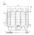
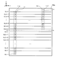
- FIG. 10 is a top view showing a schematic configuration of the active matrix substrate in the present embodiment.
- the same reference numerals as those in the first embodiment are assigned to the same configurations as those in the first embodiment.
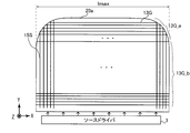
- the active matrix substrate 120a according to the present embodiment has a side opposite to the source driver 3 in the side parallel to the extending direction (X-axis direction) of the gate line 13G in the active matrix substrate 120a.
- the sides are formed in an uneven shape.
- the gate line 13G group is arranged substantially in parallel in the Y axis direction at regular intervals in each column.
- gate lines 13G of GL (1) to GL (n + a) rows are arranged.
- gate lines 13G of G (1) to G (n) rows are arranged.
- a group of source lines 15S parallel to the Y axis is formed on the active matrix substrate 120a so as to intersect with the group of gate lines 13G, and a frame on the source driver 3 side.
- a terminal portion 12s is formed in the region.
- FIG. 11 is a diagram illustrating drive timing of the active matrix substrate 120a.
- the gate driver groups 11_s1 and 11_s3 in the columns S1 and S3 sequentially drive the gate lines 13G from the GL (1) to GL (n + a) rows according to the control signals, and output set signals.
- the gate driver groups 11_s2 and 11_s4 in the columns S2 and S4 sequentially drive the gate lines 13G from the GL (1) to GL (n) rows according to the control signals, and output set signals.
- the scans of the columns S2 and S4 are finished at the timing from the start t0 to t1, and the scans of the rows S1 and S3 are finished at the timing t2.
- the gate line 13G having a length corresponding to the width of the concavo-convex portion is formed on the active matrix substrate 120a, and the gate line 13G By forming the gate driver 11 between them, the display can be controlled for each display region corresponding to the width of the uneven portion. Further, the scanning time of the gate lines 13G in the columns (S2, S4) in which the concave portions are formed is shorter than the scanning time of the gate lines 13G in the columns (S1, S3) in which the convex portions are formed.
- the data signal whose signal amplitude is minimized is output until the scanning of the column in which the convex portion is formed is completed. Therefore, it is possible to reduce the power consumption for driving the source line 15S in the column in which the recess is formed.
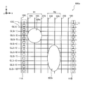
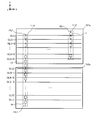
- FIG. 12A is a top view showing a schematic configuration of the active matrix substrate in the present embodiment.
- symbol as 1st Embodiment is attached
- a configuration different from the first embodiment will be described.
- a non-display area 300 is formed in a display area 200 indicated by a broken line.
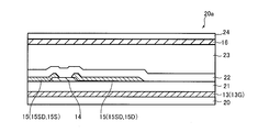
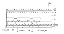
- FIG. 12B is a diagram showing a cross section of the display panel 2 taken along the line II shown in FIG. 12A.
- the element layer 10 including the gate wiring layer 13, the source wiring layer 15, the semiconductor layer 14, and the like is formed in the display region 200 on the substrate 20 of the active matrix substrate 220a.
- the element layer 10 is not formed in the non-display area 300.
- the liquid crystal layer 40 between the active matrix substrate 20 a and the counter substrate 20 b is formed in the non-display area 300 and the display area 200.
- the polarizing plate 30A on the counter substrate 20b side and the polarizing plate 30B on the active matrix substrate 20a side are formed in the display area 200, and a hole 300H is formed in the non-display area 300 portion.
- the hole 300H is not formed in the portion of the non-display region 300 in the substrate 20 and the counter substrate 20b, and the element layer 10 and the polarization are not formed in the portion of the non-display region 300.
- the plates 30A and 30B are not formed.
- the source line 15S formed in the columns S2 and S4 and routed to the frame region 301 is formed. Therefore, the source line 15S formed in the region S31 and the source line 15S in the region S32 are not connected. Therefore, a data signal is supplied to the region S32 from the source driver 3 side along the scanning direction of the gate line 13G, but the region S31 is supplied from the frame region 301 side via the source lines 15S of the columns S2 and S4. A data signal is provided. That is, in the region S31, since the scanning direction of the gate line 13G is opposite to the scanning direction of the other regions, data is written in the order of GL (n + a) to GL (n).
- the active matrix substrate 320a in this embodiment has a non-display area 300 formed in the display area 200, as in the third embodiment.
- a gate line 13G group having a length substantially the same as the width of the column is formed, and a gate driver 11 is formed between the gate lines 13G in the columns S1 and S4.
- each row from GL (k + 1) to GL (n) in which the non-display region 300 is formed has a gate line 13G having a length substantially the same as the width of the column S2. Yes.
- the pixel region 250 is a pixel region where the gate driver 11 is not formed.
- a bypass wiring 15 ⁇ / b> SL made of the source wiring layer 15 is formed substantially in parallel with the source line 15 ⁇ / b> S between the source lines 15 ⁇ / b> S constituting the pixel region 250.
- a bypass wiring 13n connected to the bypass wiring 15SL via the contact portion CH2 is formed substantially parallel to the gate line 13G.
- the bypass wiring 13n includes the gate wiring layer 13, and the contact portion CH2 is formed in the same manner as in FIG. 7D of the first embodiment.
- the detour wiring 13n is formed up to the source line 15S formed in the pixel region 251 of the column S3 shown in FIG.
- the display control circuit 4 is similar to the above in the case of the seal material vicinity region S1, for the gate driver 11 in the seal material vicinity region S1, S2.
- a control signal for driving the gate line 13G of S2 at 60 Hz is input through the terminal portion 12g.
- a control signal for driving the gate line 13G in the region S3 at 1 Hz is input to the gate driver 11 in the region S3 via the terminal portion 12g.
- the region near the two sides parallel to the Y axis in the display region 200 is described as an example of the region near the sealing material.
- the two sides parallel to the X axis in the display region 200 are described. It may be a nearby region or a region near the four sides of the display region 200.
- FIG. 20 is a diagram illustrating an example of an equivalent circuit of the gate driver 11 ′.
- the gate driver 11 ' is formed between the gate lines 13G of GL (n-1) and GL (n).
- the gate driver 11 ′ receives the set signal (S) from the gate driver 11 ′ (previous stage gate driver) that scans the gate line 13G of GL (n ⁇ 1), and the gate line of GL (n) according to the control signal. 13G is driven and a set signal (S) is output to the gate driver 11 ′ (next stage gate driver) that drives the gate line 13G of GL (n + 1).
- the gate driver 11 ′ has TFT-A to TFT-M switching elements composed of TFTs, a capacitor Cbst, terminals 111 to 124, and a low-level power supply voltage signal (VSS). Input terminal group. That is, the gate driver 11 'includes TFT-K, TFT-L, TFT-M, and terminals 121 to 124 in addition to the switching element of the gate driver 11 of the first embodiment shown in FIG.
- the H level potential of the clock signal (CKA) is output from the terminal 120 to the gate line 13G of GL (n).
- the netC H-level potential is input from the terminal 124 to the terminals 111 and 112 of the next-stage gate driver 11 ′ as the set signal (S) of the next-stage gate driver 11 ′.
- the netC H level potential is output from the terminal 124 to the terminal 123 of the preceding gate driver 11 ′ as a signal (R) of the preceding gate driver 11 ′.
- FIG. 21B is a timing chart showing scanning of the gate line 13G when the row selection signal (EN) indicating VSS (L level) is input to the gate driver 11 '.
- the description up to time t2 is omitted because it is the same as FIG. 21A.
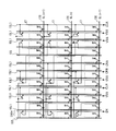
- FIG. 23A is a diagram illustrating data of each frame to be written in each area of columns S1 to S4 in display area 200.
- data of V101, V102... V160 is written for each frame of F1 to F60.
- data of V201, V202... V260 are written for each frame of F1 to F60.
- data of V301, V302... V360 are written for each frame of F1 to F60.
- data of V401, V402... V460 is written for each frame of F1 to F60.
- each gate driver 11 ′ in the columns S1 to S4 scans the gate line 13G in each column at a driving frequency of 60 Hz in accordance with the clock signal (CKA, CKB), and as shown in FIG. ) To GL (n), the gate line 13G is driven.
- FIG. 24B is a diagram showing the drive timing of the first frame.
- a row selection signal (EN) indicating VDD (H level) is input from the display control circuit 4 to the gate driver 11 ′ in each column.
- clock signals (CKA, CKB) are supplied to the gate drivers 11 ′ so that the gate lines 13 ⁇ / b> G in each column are driven at a driving frequency of 60 Hz.
- the data signal of the first frame shown in FIG. 24A is input from the source driver 3 to the source line 15S (see FIG. 22) formed in each column region at a driving frequency of 60 Hz.
- FIG. 24B one frame output to the source line 15S (see FIGS. 22A and 22B) in each column at the timing when the gate lines 13G of GL (1) to GL (n) are sequentially driven.
- the data of the eye data signal is written into the pixel area.
- the display control circuit 4 From the second frame to the 60th frame, the display control circuit 4 outputs a row selection signal (EN) indicating VSS (L level) to the gate driver 11 ′ in each column, and the source driver 3 determines the potential of the common electrode. Is output to the source line 15S (see FIGS. 22A and 22B).
- the gate lines 13G of GL (1) to GL (n) in each column are not driven, and the data signal output to the source line 15S (see FIGS. 22A and 22B) in each column. No data is written.
- the gate line 13G is driven only for the first frame, and the driving of the gate line 13G is stopped for 2 to 60 frames, thereby saving power. .
- the display control circuit 4 stops the supply of the clock signals (CKA, CKB) during the 2nd to 60th frames. It may be. With this configuration, power consumption can be further reduced.
- FIG. 26 is a diagram illustrating data of each frame to be written in each area of columns S1 to S4 in display area 200.
- control is performed so that data is written to the areas of the columns S1 and S4 only for the first frame and data is not written for the second to 60th frames. To do.
- the region P displays a moving image and displays a still image in a region other than the region P. Therefore, the source driver 3 continues until the first frame scan of the gate line 13G in the columns S2 and S3 is completed.
- a data signal indicating V201 and V301 to be displayed in each area of columns S2 and S3 is output to source line 15S (see FIGS. 22A and 22B) in columns S2 and S3.
- the display control circuit 4 inputs a row selection signal (EN) indicating VDD (H level) to the gate driver 11 ′ in the columns S1 to S4 so as to drive the gate line 13G at a driving frequency of 60 Hz.
- EN row selection signal
- CKA clock signals
- FIG. 23B data (V101 to V401) for each column in the first frame is written to the display area 200 at the timing when the gate lines 13G in each column are sequentially driven.
- the display control circuit 4 supplies a row selection signal (EN) indicating VSS (L level) to the gate drivers 11 'in the columns S1 and S4 after the second frame.
- the row selection signal (EN) indicating VSS (L level) is supplied during the scanning period of the gate line 13G of GL (1) to GL (k ⁇ 1).
- a row selection signal (EN) indicating VDD (H level) is supplied in the scanning period of the gate line 13G from GL (k) to GL (l).
- a row selection signal (EN) indicating VSS (L level) is supplied during the scanning period of the gate line 13G of GL (l + 1) to GL (n).
- the regions of the column S2 and the column S3 are row-selected for the scanning period of the gate lines 13G of GL (k) to GL (l) for each frame. Data is written into the region P at the timing when the signal (EN) becomes H level and the gate lines 13G of GL (k) to GL (l) are sequentially driven.
- the regions of the column S1 and the column S4 have the row selection signal (EN) while the gate lines 13G of GL (1) to GL (n) are scanned. ) Becomes L level, the gate lines 13G in the columns S1 and S4 are not driven, and data is not written.
- the active matrix substrate 620a has terminal portions 12sa and 12sb for supplying data signals.
- the terminal portions 12sa and 12sb are provided on two sides substantially parallel to the extending direction (x-axis direction) of the gate line 13G in the frame region.
- a source driver 3a is provided outside the active matrix substrate 620a on the side where the terminal portion 12sa is provided.
- the terminal portion 12sa is connected to the source driver 3a.
- a source driver 3b is provided outside the active matrix substrate 620a on the side where the terminal portion 12sb is provided.
- the terminal portion 12sb is connected to the source driver 3b.
- the source driver 3a and the source driver 3b simultaneously output the same data signal to the terminal portions 12sa and 12sb, respectively.
- the terminal portion 12g is not shown, but the terminal portion 12g is provided in the frame area where the terminal portion 12sa is provided.
- the power supply 5 (see FIG. 14 and the like) is not shown, but the power supply 5 is provided on the side where the terminal portion 12g is provided, as in the third embodiment.
- the active matrix substrate 620a, the display control circuit 4, and the source drivers 3a and 3b are supplied with a power supply voltage signal from the power supply 5.
- the active matrix substrate 620a has non-display areas 300a and 300b between the gate driver groups 11A and 11B, and a non-display area 300c between the gate driver groups 11B and 11C.
- the gate line 13G and the source line 15S intersecting in the non-display areas 300a, 300b, and 300c are divided in the non-display areas 300a, 300b, and 300c.
- the portion of the source line 15S where the non-display areas 300a, 300b, and 300c are not arranged is extended from the terminal portion 12sa to the terminal portion 12sb and connected to the terminal portion 12sa and the terminal portion 12sb. Therefore, the data signal output from the source driver 3a is supplied to the source line 15S in the portion where the non-display regions 300a, 300b, and 300c are not disposed through the terminal portion 12sa and is output from the source driver 3b. A data signal is supplied via the terminal portion 12sb.
- FIG. 28B shows a schematic diagram in which a portion where the non-display areas 300a and 300b in FIG. 28A are arranged is enlarged.
- the source line 15S arranged in the x-axis direction width R1 of the non-display area 300a and the non-display area 300b in the x-axis direction width R2 There is a break near the boundary between 300a and 300b.
- the source line 15S arranged on the terminal part 12sa side is supplied with a data signal via the terminal part 12sa and the source line 15S arranged on the terminal part 12sb side.
- the line 15S is supplied with a data signal via the terminal portion 12sb.
- the gate lines 13G of GL (k-3) to GL (k-1) on the right side (x-axis positive direction side) divided in the non-display area 300a are GL (k-3) to GL in the gate driver group 11B. It is driven by a gate driver 11 that drives GL (k ⁇ 1).
- the gate lines 13G of GL (k-10) to GL (k-5) on the left side (x-axis negative direction side) divided in the non-display area 300b are GL (k-10) to GL in the gate driver group 11A. It is driven by a gate driver 11 that drives GL (k-5).
- the gate lines 13G of GL (k-10) to GL (k-5) on the right side (x-axis positive direction side) divided in the non-display area 300b are GL (k-10) to GL in the gate driver group 11B. It is driven by a gate driver 11 that drives GL (k-5).
- the portion of the source line 15S where the non-display area is not arranged may be configured such that a data signal is supplied from either one of the source drivers 3a and 3b.
- the other source driver stops outputting the data signal to the source line 15S in the portion where the non-display area is not arranged.
- the source line 15S in the portion where the non-display area is not disposed may be configured to be connected to either the terminal portion 12sa or the terminal portion 12sb and not connected to the other.
- the terminal portion 12sb is disposed in the frame region on the short side of the two substantially parallel sides of the active matrix substrate 621a, and the terminal portion 12sa is disposed in the frame region on the long side. Yes.
- the terminal portion 12sb is connected to the source line 15S formed in the region R30 having substantially the same width as the short side of the active matrix substrate 621a.
- the terminal portion 12sa is connected to the source line 15S formed in the regions R31 and R32 excluding the region R30 in the active matrix substrate 621a.
- the terminal part 12g is provided in the frame area
- the terminal portion 12sa is outside the active matrix substrate 621a and is provided on the side where the terminal portion 12sa is arranged, as in FIG. 28A described above. It is connected to the driver 3a.
- the terminal portion 12sb is connected to the source driver 3b provided outside the active matrix substrate 621a and on the side where the terminal portion 12sb is disposed.
- the terminal unit 12sa supplies the data signal output from the source driver 3a to the source line 15S formed in the regions R31 and R32.
- the terminal unit 12sb supplies the data signal output from the source driver 3b to the region R30. This is supplied to the formed source line 15S.
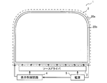
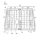
- the outer shape of the active matrix substrate 20a of the first embodiment described above has an arc shape at the left and right upper end portions, and the widths of the other portions excluding the arc shape portion are substantially equal. Yes.
- the display area formed on the active matrix substrate 20a has the same shape as the outer shape.
- an example of a method for manufacturing such an active matrix substrate 20a will be described.
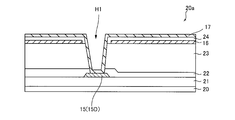
- a gate wiring layer 13, a gate insulating film 21, a semiconductor layer 14, a source wiring layer 15, a protective layer 22, a protective layer 23, and a shield layer 16 are provided on a substantially rectangular substrate 20, as shown in FIGS. 7A to 7D.
- the interlayer insulating layer 24 and the pixel electrode 17 are sequentially formed to form an active matrix substrate (first active matrix substrate) having a substantially rectangular display region.
- the first active matrix substrate has a plurality of gate lines 13G having substantially the same length and arranged at regular intervals, and arranged at regular intervals so as to intersect with the gate lines 13G.
- the plurality of source lines 15S thus formed are formed, and each layer necessary for display is formed.
- each layer formed on the substrate 20 is etched into a shape similar to the outer shape of the active matrix substrate 20a shown in FIG. That is, a part of each layer formed on the first active matrix substrate is removed so that a part of the gate lines 13G is shorter than the maximum length of the display region in the extending direction of the gate lines 13G. Then, after all the layers on the first active matrix substrate are etched, the substrate 20 is processed into a predetermined shape.
- a resist is applied to the substrate 20, and the substrate 20 is etched with an etching solution containing hydrofluoric acid or ammonium hydrogen fluoride and / or ammonium phosphate using the predetermined mask pattern. Thereby, the substrate 20 is etched into a predetermined shape, and an active matrix substrate 20a (second active matrix substrate) illustrated in FIG. 2 is formed.
- the cutting of the substrate 20 is not limited to the etching method using hydrofluoric acid or the like, and may be cut using a diamond cutter or may be cut using a grinder.
- the first active matrix substrate After the first active matrix substrate is generated, the first active matrix substrate, the first active matrix substrate bonded to the counter substrate, or the liquid crystal layer between the first active matrix substrate and the counter substrate You may make it perform the cutting
- a resist may be applied and etched using an etchant containing hydrofluoric acid or ammonium hydrogen fluoride and / or ammonium phosphate using the predetermined mask pattern.
- the first manufacturing method after all the layers are formed on the substantially rectangular substrate 20 to generate the first active matrix substrate having the substantially rectangular display region, at least a part of the gate lines 13G is gated. A part of the first active matrix substrate is removed so as to be shorter than the maximum length of the width of the display region in the extending direction of the line 13G, thereby generating a second active matrix substrate.
- the second manufacturing method described below each time a layer is formed on the substrate 20, a part of the layer is removed to generate a second active matrix substrate.
- the second manufacturing method will be described.
- FIG. 30A is a top view schematically showing a state in which the gate wiring layer 13 is formed on the substrate 20.
- a plurality of gate lines 13G having substantially the same length are formed at regular intervals substantially in parallel.
- a resist is applied on the gate wiring layer 13, and the gate wiring layer 13 is etched using a predetermined mask pattern.
- FIG. 30B the part of the gate line 13G formed outside the shape P corresponding to the predetermined mask pattern in FIG. 30A is removed.
- the arc-shaped portion of the gate line 13G is shorter than the other gate lines 13G.
- a gate insulating film 21 is formed on the gate wiring layer 13
- a resist is applied on the gate insulating film 21, and gate insulation is performed using a predetermined mask pattern.
- the film 21 is etched. Thereby, the gate insulating film 21 formed outside the shape P corresponding to the predetermined mask pattern is removed (not shown).
- the source wiring layer 15 is formed on the semiconductor layer 14. Thereby, as shown in FIG. 30C, source lines 15S having substantially the same length are formed at regular intervals so as to intersect with the gate line 13G. After the formation of the source wiring layer 15, a resist is applied on the source wiring layer 15, and the source wiring layer 15 is etched using a predetermined mask pattern. Thus, as shown in FIG. 30D, the source wiring layer 15 formed outside the shape P corresponding to the predetermined mask pattern in FIG. 30C is removed.
- a protective layer 22, a protective layer 23, a shield layer 16, an interlayer insulating layer 24, a pixel electrode 17, and contact holes H1 and H2 are sequentially formed (illustrated). (Omitted).
- a resist is applied and etched with a predetermined mask pattern.
- each layer on the substrate 20 is etched into a shape similar to the outer shape of the active matrix substrate 20a shown in FIG.
- a resist is applied to the substrate 20 and the substrate 20 is etched with a predetermined mask pattern, thereby finally generating a second active matrix substrate.
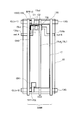
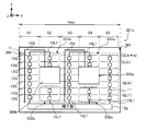
- the active matrix substrate 720a has gate lines 13G of GL (1) to GL (n).
- the active matrix substrate 720a includes gate driver groups 11 ⁇ and 11 ⁇ .
- the gate driver group 11 ⁇ includes a gate driver 11 provided for each of the gate lines 13G of GL (1) to GL (n).
- the gate driver group 11 ⁇ includes the gate drivers 11 provided for the gate lines 13G of GL (k + 1) to GL (n).
- the gate drivers 11 in the gate driver groups 11 ⁇ and 11 ⁇ are connected by the wiring 15L1 as in the first embodiment.
- a gate line 13G is formed between a portion where the gate driver group 11 ⁇ is formed and a portion where the gate driver group 11 ⁇ is not formed. Cut along.
- the active matrix substrate 720a is cut at a position based on the cutting line H between the gate lines 13G of GL (k) and GL (k + 1).
- two active matrix substrates 721a and 722a are generated as shown in FIG. 31B.
- the active matrix substrates 721a and 722a are etched using a predetermined mask pattern, thereby obtaining the same shape as the active matrix substrate 20a illustrated in FIG.
- the active matrix substrates 721a and 722a (see FIGS. 31C and 31D) having the second active matrix substrate are generated.
- a terminal portion 12g is provided on the side of the active matrix substrate 722a where the gate line 13G of the GL (1) is disposed in the frame region.
- the gate driver group 11 ⁇ and the terminal portion 12g are connected.
- the start pulse signal output from the display control circuit 4 is supplied to the gate driver 11 that drives the gate line 13G of the GL (1) of the gate driver group 11 ⁇ via the terminal portion 12g.
- a control signal (clock signal or the like) output from the display control circuit 4 is supplied to the gate driver group 11 ⁇ via the terminal portion 12g.
- the gate lines 13G are sequentially driven in the order of GL (1) to GL (k).
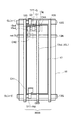
- a terminal portion 12g is provided on the side where the GL (1) gate line 13G is arranged in the frame region, and the gate The driver group 11 ⁇ and the terminal portion 12g are connected.
- the start pulse signal from the display control circuit 4 is supplied to the gate driver 11 that drives the gate line 13G of GL (1) through the terminal portion 12g.
- the gate line 13G is driven in the order of GL (1) to GL (n) in accordance with a control signal (clock signal or the like) from the display control circuit 4.
- the gate driver group 11 ⁇ is not driven because no control signal is supplied.
- Application example 2 In the application example 1 described above, the example in which the active matrix substrate 720a is cut in substantially parallel to the extending direction of the gate line 13G has been described. However, the active matrix substrate 720a is cut in a direction substantially orthogonal to the extending direction of the gate line 13G. An active matrix substrate may be generated.
- the active matrix substrate 720a is cut up and down or left and right to generate two active matrix substrates.
- the first active matrix substrate is cut up and down and left and right to form four active matrix substrates.
- a second active matrix substrate may be generated.
- FIG. 33A is a top view schematically showing a schematic configuration of the first active matrix substrate according to this application example.
- the source line 15S is not shown.
- alternate long and short dash lines H1 and H2 indicate reference positions for cutting, and are hereinafter referred to as cutting lines H1 and H2.
- an active matrix substrate 820a which is an example of a first active matrix substrate, includes gate driver groups 11 ⁇ L and 11 ⁇ L in left and right regions separated by a cutting line H1 substantially orthogonal to the extending direction of the gate line 13G.
- Gate driver groups 11 ⁇ R and 11 ⁇ R are formed.
- the gate driver groups 11 ⁇ L and 11 ⁇ R include gate drivers 11 provided for the gate lines 13G of GL (1) to GL (n).
- the gate driver groups 11 ⁇ L and 11 ⁇ R include gate drivers 11 provided for the gate lines GL (n) to GL (k + 1).
- the active matrix substrate 820a includes a gate driver (first gate line driving circuit) provided for each gate line 13G and a gate driver (second gate driver) provided for each of some adjacent gate lines 13G.
- a gate driver first gate line driving circuit
- second gate driver second gate driver
- a plurality of pairs 11 ⁇ L and 11 ⁇ L, 11 ⁇ R and 11 ⁇ R are formed.
- the active matrix substrates 821a, 822a, 823a, and 824a are generated by cutting the active matrix substrate 820a with reference to the positions of the cutting lines H1 and H2, as shown in FIG. 33B. That is, in the active matrix substrate 820a, the pair of the first gate line driving circuit and the second gate line driving circuit is cut along the source line 15S (not shown), thereby forming the second active matrix substrate. As an example, four active matrix substrates 821a, 822a, 823a, and 824a are generated.
- the active matrix substrate 823a is provided with a part of the gate driver group 11 ⁇ L
- the active matrix substrate 824a is provided with a part of the gate driver group 11 ⁇ R.
- Each of the gate driver groups 11 ⁇ L and 11 ⁇ R in the active matrix substrates 823a and 824a includes the gate driver 11 provided for the gate lines 13G of GL (1) to GL (k).
- the active matrix substrate 823a and the active matrix substrate 824a are connected to the gate driver groups 11 ⁇ L and 11 ⁇ R, respectively, in the same manner as the active matrix substrate 722a shown in FIG. 31D described above.
- a terminal portion 12g is provided.
- the gate lines 13G are driven in the order of GL (1) to GL (k) by the gate driver groups 11 ⁇ L and 11 ⁇ R.
- first active matrix substrate a plurality of active matrix substrates (first active matrix substrates smaller in size than the first active matrix substrate). 2 active matrix substrates). Therefore, the production line is made more efficient and the production cost can be reduced as compared with the case where an active matrix substrate is produced for each display size (number of pixels).
- the pixels in the cut portion are lost by cutting the first active matrix substrate. Therefore, it is preferable to design the first active matrix substrate in consideration of the number of pixels lost by the cut portion. For example, when the active matrix substrate 820a illustrated in FIG. 33A corresponds to a display having the number of pixels “8K4K” (7680 ⁇ 4320), the number of pixels of the active matrix substrate 820a is set to (8K + 100 pixels) ⁇ (4K + 50 pixels) or the like. As described above, the number of pixels is increased from “8K4K” (7680 ⁇ 4320).
- a wiring pattern of the terminal portion 12s for supplying the data signal from the source driver 3 to the source line 15S is formed.
- the wiring pattern of the terminal portion 12s is also cut, and the pixel that cannot supply the data signal in the cut active matrix substrate. May occur.
- a first active matrix substrate is generated so that a pixel to which no data signal is supplied does not occur in a cut active matrix substrate.
- FIG. 34A is a schematic view illustrating a part of the first active matrix substrate according to this application example.
- the terminal groups 12s_2 and 12s_5 including are formed.
- terminal portions 12s are connected to, for example, 360 source lines 15S.
- the terminal groups 12s_2 and 12s_5 include 14 terminal portions 12s.
- the active matrix substrate 920a is provided with one or a plurality of gate drivers 11 for each divided gate line 13G.
- Gate driver groups 11a and 11b are connected to the gate line 13G intersecting the source line 15S connected to the terminal portion 12s_1, the terminal group 12s_2, and the terminal portion 12s_3.
- the gate driver group 11c is connected to the gate line 13G that intersects the source line 15S connected to the terminal portion 12s_4.
- Gate driver groups 11d and 11e are connected to the gate line 13G intersecting the source line 15S connected to the terminal group 12s_5 and the terminal portion 12s_6.
- a gate driver group 11f is connected to the gate line 13G that intersects the source line 15S connected to the terminal portion 12s_7.
- the active matrix substrate 920a When an active matrix substrate for display having a first number of pixels (for example, 3840 ⁇ 1080) is generated from the active matrix substrate 920a, the active matrix substrate 920a is cut at the position of the pixel region between H13 and H10 in FIG. 34A. To do. Thereby, the pixel region between H13 and H10, that is, the pixel region driven by the gate driver group 11f is cut, and driven by the 32 terminal portions 12s (12s_1 to 12s_6) and the gate driver groups 11a to 11e. An active matrix substrate is generated.
- a first number of pixels for example, 3840 ⁇ 1080
- the gate lines 13G is formed.
- a second active matrix substrate shorter than the maximum length of the display area in the extending direction of the gate line 13G is generated.
- a predetermined shape is obtained as in the first manufacturing method described above.
- the second active matrix substrate may be generated by cutting so that
- the case where the number of source lines 15S connected to one terminal portion 12s is the same has been described. Since the same source driver can be used for each terminal portion 12 s because the number of outputs of one terminal portion 12 s is the same, manufacturing costs can be reduced, design efficiency can be improved, and display can be made uniform. Can do. However, the number of terminals of the terminal portion 12s_4 and the terminal portion 12s_7 can be reduced in order to minimize the pixel area that is unnecessary due to cutting. In this case, source drivers having different numbers of outputs may be prepared for the terminal portions 12s_4 and 12s_7 and the other terminal portions.
- one side parallel to the extending direction (X-axis direction) of the gate line 13G is formed in an uneven shape.
- two sides parallel to the extending direction (Y-axis direction) of the source line 15S may be formed in an uneven shape.
- portions where two sides parallel to the Y axis of the active matrix substrate 121a are formed inwardly are referred to as non-display regions 310A and 310B.
- gate lines 13G having a length substantially the same as the width in the X-axis direction of the non-display areas 310A and 310B are formed in the columns S1 and S4 where the non-display areas 310A and 310B are located. Yes.
- gate lines 13G having a length substantially the same as the width of each column are formed in the columns S2 and S3 obtained by dividing the region between the columns S1 and S4. That is, the length of each gate line 13 is shorter than the maximum length lmax of the width in the X-axis direction in the active matrix substrate 121a.
- a gate driver 11 is formed in the column S3 between the gate lines 13G in the columns S3 and S4. Accordingly, in this example, the gate driver 11 is not formed in the regions S31b and S32b of the column S1 where the non-display regions 310A and 310B are formed and the regions S31a and S32a of the column S4.
- one non-display area 300 is formed in the display area 200.
- a plurality of non-display areas 300a and 300b may be formed.
- gate lines having substantially the same length as the width in the X-axis direction of the non-display areas 300a and 300b. 13G is formed. Gate lines 13G having substantially the same length are formed in the columns S1, S3, and S5 in which the non-display areas 300a and 300b are not formed. Each gate line 13G is long enough to form at least one gate driver 11.
- the source lines 15S are formed so as to intersect with the gate lines 13G in each column.
- the terminal portion 12s for supplying the data signal from the source driver 3 to each source line 15S is arranged in a frame region where the terminal portion 12g is formed.
- the source lines 15S of the regions S31a and S31b on the frame region 301 side in the columns S2 and S4 are routed to one of the source regions 15S of the columns S1 and S3 to the frame region 301, and the regions S31a, S31, It is formed by being folded back to 31b.
- the gate driver 11 in the regions S31a and 31b is routed to the frame region 301 by the wiring 15L1 connecting the gate drivers 11 in the columns S3 and S1 and folded back to the regions S31a and 31b.
- the gate drivers 11 in the columns S3 and S1 are connected.
- a gate driver 11 is formed in the column S1 between the gate lines 13G in the columns S1 and S2.
- a gate driver 11 is formed in the column S5 between the gate lines 13G in the columns S4 and S5. Accordingly, in this example, the gate driver 11 is not formed in the regions S31b and S32b of the column S2 where the non-display regions 300a and 300b are formed and the regions S31a and S32a of the column S4.
- the source lines 15S in the regions S31a and S32a sandwiching the non-display region 300a are connected to the bypass wirings 15SL and 13b (in the pixel region of the column S3). (See FIGS. 15 and 16). Further, the source lines 15S in the regions S31b and 32b sandwiching the non-display region 300b may be connected via detour wirings 15SL and 13b (see FIGS. 15 and 16) formed in the pixel region of the column S1.
- the gate driver 11 ′ in the seventh embodiment may be used instead of the gate driver 11.
- the gate driver 11 ′ By using the gate driver 11 ′, the gate line 13 ⁇ / b> G group in the display region 200 can be driven for each row.
- an arbitrary gate line when displaying a still image, an example in which an arbitrary gate line is driven only in the first frame and driving of the arbitrary gate line is stopped in the second to 60th frames will be described. However, it may be as follows. For example, an arbitrary gate line may be driven from the first frame to the second frame, and driving of the arbitrary gate line may be stopped during the third to 60th frames. In short, it may be configured to stop driving of an arbitrary gate line in at least some frames according to the driving frequency.
- the semiconductor layer 14 of the switching element constituting the gate drivers 11 and 11 ′ is made of an oxide semiconductor.
- it may be made of polysilicon, amorphous silicon, or the like.
- the gate line 13G, the source line 15S, the gate driver 11, and the terminal portion 12g to which a control signal for the gate driver 11 is input on the substrate 20 of the active matrix substrate 20a.
- the source driver 3 and the display control circuit 4 may be formed in addition to these.
- the display panel 2 is a liquid crystal panel.
- the display panel 2 is a display panel that drives an active matrix substrate using organic EL (Electro-Luminescence) or the like. May be.
- At least a part of the gate lines 13G is shorter than the maximum length of the display area in the extending direction of the gate lines 13G.
- the example of removing a part of the active matrix substrate has been described. However, when an active matrix substrate used for a substantially rectangular display is generated, a step of removing a part of the active matrix substrate is not performed. . That is, for example, an active matrix substrate (721a and 722a in FIG. 31B) obtained by cutting the first active matrix substrate 720a illustrated in FIG. 31A with reference to the position indicated by the cutting line H may be used for the display. Alternatively, an active matrix substrate obtained by cutting the first active matrix substrate 720a shown in FIG.
- an active matrix substrate (821a to 824a in FIG. 33B) obtained by cutting the first active matrix substrate 820a shown in FIG. 33A with reference to the positions indicated by the lines H1 and H2 may be used for the display.
- a matrix substrate (921a and 922a in FIG. 34B) may be used for the display.
- the present invention can be used for a display including a display panel using liquid crystal, organic EL, or the like.
Abstract
Priority Applications (3)
| Application Number | Priority Date | Filing Date | Title |
|---|---|---|---|
| US14/775,933 US9685131B2 (en) | 2013-03-15 | 2014-03-12 | Active-matrix substrate, method of manufacturing active-matrix substrate, and display panel |
| JP2015505521A JP6230074B2 (ja) | 2013-03-15 | 2014-03-12 | アクティブマトリクス基板およびアクティブマトリクス基板の製造方法 |
| CN201480015706.3A CN105164743B (zh) | 2013-03-15 | 2014-03-12 | 有源矩阵基板、有源矩阵基板的制造方法以及显示面板 |
Applications Claiming Priority (4)
| Application Number | Priority Date | Filing Date | Title |
|---|---|---|---|
| JP2013054294 | 2013-03-15 | ||
| JP2013-054294 | 2013-03-15 | ||
| JP2013-208585 | 2013-10-03 | ||
| JP2013208585 | 2013-10-03 |
Publications (1)
| Publication Number | Publication Date |
|---|---|
| WO2014142183A1 true WO2014142183A1 (fr) | 2014-09-18 |
Family
ID=51536834
Family Applications (1)
| Application Number | Title | Priority Date | Filing Date |
|---|---|---|---|
| PCT/JP2014/056527 WO2014142183A1 (fr) | 2013-03-15 | 2014-03-12 | Substrat à matrice active, procédé de fabrication de substrat à matrice active et panneau d'affichage |
Country Status (4)
| Country | Link |
|---|---|
| US (1) | US9685131B2 (fr) |
| JP (1) | JP6230074B2 (fr) |
| CN (1) | CN105164743B (fr) |
| WO (1) | WO2014142183A1 (fr) |
Cited By (35)
| Publication number | Priority date | Publication date | Assignee | Title |
|---|---|---|---|---|
| WO2015033838A1 (fr) * | 2013-09-04 | 2015-03-12 | シャープ株式会社 | Substrat à matrice active, panneau d'affichage et dispositif d'affichage le comprenant |
| WO2015190488A1 (fr) * | 2014-06-13 | 2015-12-17 | シャープ株式会社 | Circuit de registre à décalage et dispositif d'affichage contenant ledit circuit |
| CN105527739A (zh) * | 2014-10-16 | 2016-04-27 | 乐金显示有限公司 | 用于具有窄边框的显示装置的面板阵列 |
| WO2016080498A1 (fr) * | 2014-11-21 | 2016-05-26 | シャープ株式会社 | Substrat de matrice active et panneau d'affichage |
| CN105761670A (zh) * | 2014-12-31 | 2016-07-13 | 三星显示有限公司 | 非四边形显示器及其驱动方法 |
| WO2016140281A1 (fr) * | 2015-03-02 | 2016-09-09 | シャープ株式会社 | Substrat à matrice active et dispositif d'affichage équipé de celui-ci |
| WO2016143659A1 (fr) * | 2015-03-10 | 2016-09-15 | シャープ株式会社 | Dispositif d'affichage |
| WO2016190229A1 (fr) * | 2015-05-28 | 2016-12-01 | シャープ株式会社 | Système de gestion de production d'écrans d'affichage et procédé de gestion de production d'écrans d'affichage |
| KR20170012683A (ko) * | 2015-07-22 | 2017-02-03 | 삼성디스플레이 주식회사 | 표시 장치 |
| WO2017038661A1 (fr) * | 2015-09-04 | 2017-03-09 | シャープ株式会社 | Procédé de fabrication de panneaux à cristaux liquides |
| KR20170046841A (ko) * | 2015-10-21 | 2017-05-04 | 삼성디스플레이 주식회사 | 액정 표시 장치 |
| JP2017113451A (ja) * | 2015-12-25 | 2017-06-29 | 株式会社ユニバーサルエンターテインメント | 遊技機 |
| US20170255074A1 (en) * | 2014-11-21 | 2017-09-07 | Sharp Kabushiki Kaisha | Active matrix substrate and display panel |
| WO2017170099A1 (fr) * | 2016-03-30 | 2017-10-05 | シャープ株式会社 | Procédé de fabrication de panneaux à cristaux liquides |
| CN107274846A (zh) * | 2016-04-08 | 2017-10-20 | 株式会社日本显示器 | 显示装置 |
| WO2018030207A1 (fr) * | 2016-08-08 | 2018-02-15 | シャープ株式会社 | Dispositif d'affichage |
| WO2018033817A1 (fr) * | 2016-08-17 | 2018-02-22 | 株式会社半導体エネルギー研究所 | Dispositif d'affichage et appareil électronique |
| WO2018051943A1 (fr) * | 2016-09-13 | 2018-03-22 | シャープ株式会社 | Dispositif d'affichage |
| KR20180042351A (ko) * | 2015-09-28 | 2018-04-25 | 애플 인크. | 연장된 활성 영역을 갖는 전자 디바이스 디스플레이 |
| WO2018190206A1 (fr) * | 2017-04-11 | 2018-10-18 | シャープ株式会社 | Dispositif d'affichage |
| KR20190009386A (ko) | 2016-09-16 | 2019-01-28 | 도판 인사츠 가부시키가이샤 | 표시 장치 및 표시 장치 기판 |
| KR20190025496A (ko) * | 2017-09-01 | 2019-03-11 | 애플 인크. | 디스플레이들을 위한 데이터 신호 조정 |
| JP2019061202A (ja) * | 2017-09-28 | 2019-04-18 | 株式会社ジャパンディスプレイ | 表示装置 |
| JP2019070744A (ja) * | 2017-10-10 | 2019-05-09 | 三菱電機株式会社 | 液晶表示装置 |
| US10347208B2 (en) | 2016-07-04 | 2019-07-09 | Samsung Dispiay Co., Ltd. | Display device |
| WO2019198163A1 (fr) * | 2018-04-10 | 2019-10-17 | シャープ株式会社 | Dispositif d'affichage |
| WO2020040246A1 (fr) * | 2018-08-23 | 2020-02-27 | 株式会社ジャパンディスプレイ | Dispositif d'affichage |
| JP2020060697A (ja) * | 2018-10-10 | 2020-04-16 | シナプティクス インコーポレイテッド | 表示ドライバ、プログラム、記憶媒体及び表示画像データの生成方法 |
| JP2020112770A (ja) * | 2019-01-15 | 2020-07-27 | 三星ディスプレイ株式會社Samsung Display Co.,Ltd. | 表示装置 |
| JP2020536261A (ja) * | 2017-12-07 | 2020-12-10 | 京東方科技集團股▲ふん▼有限公司Boe Technology Group Co.,Ltd. | 表示パネル、表示装置及び表示パネルを製造する方法 |
| JP2021021945A (ja) * | 2019-07-29 | 2021-02-18 | エルジー ディスプレイ カンパニー リミテッド | 貫通ホールを有する表示装置 |
| CN113419368A (zh) * | 2019-03-20 | 2021-09-21 | 厦门天马微电子有限公司 | 一种阵列基板及显示装置 |
| JP2022171731A (ja) * | 2018-08-21 | 2022-11-11 | アップル インコーポレイテッド | 開口部に適応するデータ線を有するディスプレイ |
| US11852938B2 (en) | 2018-08-21 | 2023-12-26 | Apple Inc. | Displays with data lines that accommodate openings |
| WO2024045988A1 (fr) * | 2022-09-01 | 2024-03-07 | 京东方科技集团股份有限公司 | Substrat d'affichage, panneau d'affichage et appareil d'affichage |
Families Citing this family (58)
| Publication number | Priority date | Publication date | Assignee | Title |
|---|---|---|---|---|
| CN106415704B (zh) * | 2014-06-06 | 2019-06-18 | 夏普株式会社 | 有源矩阵基板及显示面板 |
| US10332458B2 (en) * | 2014-09-05 | 2019-06-25 | Sharp Kabushiki Kaisha | Display device |
| KR102266064B1 (ko) * | 2014-10-15 | 2021-06-18 | 삼성디스플레이 주식회사 | 표시 패널 구동 방법, 이 방법을 수행하는 표시 패널 구동 장치 및 이 표시패널 구동 장치를 포함하는 표시 장치 |
| CN105513521B (zh) * | 2016-01-25 | 2018-04-13 | 京东方科技集团股份有限公司 | 异形显示屏图像阵列的分区显示系统及方法 |
| US10490122B2 (en) | 2016-02-29 | 2019-11-26 | Samsung Display Co., Ltd. | Display device |
| KR20170119270A (ko) | 2016-04-15 | 2017-10-26 | 삼성디스플레이 주식회사 | 표시 장치 |
| US10354578B2 (en) | 2016-04-15 | 2019-07-16 | Samsung Display Co., Ltd. | Display device |
| KR102526724B1 (ko) * | 2016-05-19 | 2023-05-02 | 삼성디스플레이 주식회사 | 표시 장치 |
| KR102605283B1 (ko) * | 2016-06-30 | 2023-11-27 | 삼성디스플레이 주식회사 | 표시 장치 |
| US10586495B2 (en) * | 2016-07-22 | 2020-03-10 | Semiconductor Energy Laboratory Co., Ltd. | Display device and electronic device |
| JP6805604B2 (ja) * | 2016-07-26 | 2020-12-23 | セイコーエプソン株式会社 | 電気光学装置および電子機器 |
| CN107807480B (zh) * | 2016-09-08 | 2021-04-20 | 株式会社日本显示器 | 显示装置 |
| US10409102B2 (en) * | 2016-09-08 | 2019-09-10 | Japan Display Inc. | Display device |
| KR102613863B1 (ko) | 2016-09-22 | 2023-12-18 | 삼성디스플레이 주식회사 | 표시 장치 |
| KR102611958B1 (ko) | 2016-09-23 | 2023-12-12 | 삼성디스플레이 주식회사 | 표시 장치 |
| KR102559096B1 (ko) | 2016-11-29 | 2023-07-26 | 삼성디스플레이 주식회사 | 표시 장치 |
| KR20180061568A (ko) * | 2016-11-29 | 2018-06-08 | 삼성디스플레이 주식회사 | 표시 장치 |
| US10608017B2 (en) * | 2017-01-31 | 2020-03-31 | Semiconductor Energy Laboratory Co., Ltd. | Display device, display module, and electronic device |
| KR20180096875A (ko) | 2017-02-21 | 2018-08-30 | 삼성디스플레이 주식회사 | 표시 장치 |
| KR102309599B1 (ko) * | 2017-04-11 | 2021-10-08 | 삼성디스플레이 주식회사 | 유기전계발광 표시장치 |
| TWI662326B (zh) * | 2018-01-15 | 2019-06-11 | 友達光電股份有限公司 | 顯示面板 |
| US10424602B2 (en) | 2017-05-12 | 2019-09-24 | Au Optronics Corporation | Display panel |
| TWI657699B (zh) * | 2017-05-12 | 2019-04-21 | 友達光電股份有限公司 | 顯示面板 |
| KR102417989B1 (ko) | 2017-05-23 | 2022-07-07 | 삼성디스플레이 주식회사 | 표시 장치 |
| US11322523B2 (en) * | 2017-07-05 | 2022-05-03 | Sharp Kabushiki Kaisha | Active matrix substrate, display device, and method of manufacturing active matrix substrate |
| CN107247379B (zh) * | 2017-07-31 | 2023-08-25 | Oppo广东移动通信有限公司 | 阵列基板、显示面板和电子设备 |
| CN107340661A (zh) * | 2017-08-18 | 2017-11-10 | 广东欧珀移动通信有限公司 | 阵列基板、显示面板和电子设备 |
| CN107845663B (zh) * | 2017-10-27 | 2020-12-08 | 武汉天马微电子有限公司 | 一种显示面板及显示装置 |
| KR102473211B1 (ko) * | 2017-11-03 | 2022-12-05 | 삼성디스플레이 주식회사 | 표시 장치 |
| US10769991B2 (en) | 2017-11-02 | 2020-09-08 | Samsung Display Co., Ltd. | Display device |
| KR102328177B1 (ko) | 2017-12-22 | 2021-11-19 | 삼성디스플레이 주식회사 | 표시 장치 |
| CN111465974B (zh) * | 2017-12-22 | 2021-09-17 | 堺显示器制品株式会社 | 显示装置以及显示装置的制造方法 |
| US20190206894A1 (en) * | 2017-12-28 | 2019-07-04 | a.u. Vista Inc. | Display systems with non-display areas |
| KR102573291B1 (ko) * | 2017-12-29 | 2023-08-30 | 엘지디스플레이 주식회사 | 발광 표시 장치 |
| CN110190087B (zh) | 2018-02-22 | 2021-08-24 | 群创光电股份有限公司 | 显示设备 |
| JP2019160174A (ja) * | 2018-03-16 | 2019-09-19 | シャープ株式会社 | 液晶表示パネル |
| JP2019159249A (ja) * | 2018-03-16 | 2019-09-19 | シャープ株式会社 | 表示装置、液晶表示装置、および有機el表示装置 |
| US10692415B2 (en) * | 2018-04-24 | 2020-06-23 | Wuhan China Star Optoelectronics Technology Co., Ltd. | Gate driving circuit of irregular screen panel and driving method |
| TWI677864B (zh) | 2018-06-28 | 2019-11-21 | 友達光電股份有限公司 | 顯示裝置 |
| CN108877624B (zh) * | 2018-06-29 | 2021-05-25 | 武汉天马微电子有限公司 | 异形显示面板和显示装置 |
| KR102586374B1 (ko) * | 2018-06-29 | 2023-10-10 | 교세라 가부시키가이샤 | 표시 장치 |
| KR20200009176A (ko) | 2018-07-17 | 2020-01-30 | 삼성디스플레이 주식회사 | 디스플레이 장치 |
| KR102516058B1 (ko) | 2018-08-17 | 2023-03-31 | 삼성디스플레이 주식회사 | 표시 패널 |
| CN109545090B (zh) * | 2018-12-29 | 2021-07-16 | 联想(北京)有限公司 | 显示屏及电子设备 |
| CN109584776B (zh) * | 2019-01-21 | 2021-12-24 | 武汉天马微电子有限公司 | 显示面板及显示装置 |
| TWI694424B (zh) * | 2019-03-29 | 2020-05-21 | 友達光電股份有限公司 | 顯示裝置及其製造方法 |
| KR20210000799A (ko) | 2019-06-25 | 2021-01-06 | 삼성디스플레이 주식회사 | 표시 장치 및 그 제조방법 |
| KR20210050050A (ko) | 2019-10-25 | 2021-05-07 | 삼성디스플레이 주식회사 | 화소 및 이를 포함하는 표시 장치 |
| CN112863414A (zh) * | 2019-11-26 | 2021-05-28 | 上海和辉光电有限公司 | 显示面板及其驱动方法 |
| TWI726564B (zh) | 2019-12-31 | 2021-05-01 | 財團法人工業技術研究院 | 具備閘極驅動器的畫素陣列及矩陣式感測器陣列 |
| CN111429828A (zh) | 2020-04-13 | 2020-07-17 | 深圳市华星光电半导体显示技术有限公司 | 一种显示面板和显示装置 |
| US11581391B2 (en) * | 2020-06-18 | 2023-02-14 | Boe Technology Group Co., Ltd. | Display panel and manufacturing method thereof, and display device |
| CN114503184B (zh) * | 2020-06-18 | 2024-02-02 | 京东方科技集团股份有限公司 | 显示面板及其制造方法、显示装置 |
| CN111613145B (zh) * | 2020-06-22 | 2022-07-08 | 京东方科技集团股份有限公司 | 异形显示面板和显示装置 |
| KR20220040578A (ko) * | 2020-09-23 | 2022-03-31 | 삼성디스플레이 주식회사 | 칩 온 필름 패키지 및 이를 포함하는 표시 장치 |
| KR20220096889A (ko) * | 2020-12-31 | 2022-07-07 | 엘지디스플레이 주식회사 | 표시 장치와 이를 이용한 멀티 스크린 표시 장치 |
| KR20220126329A (ko) * | 2021-03-08 | 2022-09-16 | 삼성디스플레이 주식회사 | 표시 장치 |
| JP2022149664A (ja) * | 2021-03-25 | 2022-10-07 | 凸版印刷株式会社 | 表示装置 |
Citations (10)
| Publication number | Priority date | Publication date | Assignee | Title |
|---|---|---|---|---|
| JPH10197851A (ja) * | 1997-01-07 | 1998-07-31 | Toshiba Corp | 液晶表示装置 |
| JP2006154022A (ja) * | 2004-11-26 | 2006-06-15 | Seiko Epson Corp | 電気光学装置、電気光学装置の検査方法及び電子機器 |
| JP2006293045A (ja) * | 2005-04-12 | 2006-10-26 | Sanyo Epson Imaging Devices Corp | 液晶パネルの製造方法および該製造方法により製造された液晶パネル |
| JP2008046598A (ja) * | 2006-07-20 | 2008-02-28 | Seiko Epson Corp | 表示装置、表示装置の駆動方法及び電子機器 |
| JP2008224802A (ja) * | 2007-03-09 | 2008-09-25 | Sharp Corp | 表示装置及びその製造方法 |
| JP2008292995A (ja) * | 2007-04-27 | 2008-12-04 | Nec Lcd Technologies Ltd | 非矩形表示装置 |
| JP2009047902A (ja) * | 2007-08-20 | 2009-03-05 | Hitachi Displays Ltd | 表示装置 |
| JP2009134246A (ja) * | 2007-11-09 | 2009-06-18 | Epson Imaging Devices Corp | 電気光学装置 |
| JP2012518199A (ja) * | 2009-02-13 | 2012-08-09 | グローバル・オーエルイーディー・テクノロジー・リミテッド・ライアビリティ・カンパニー | ディスプレイデバイス内のチップレット間のピクセルの分割 |
| JP2012518200A (ja) * | 2009-02-16 | 2012-08-09 | グローバル・オーエルイーディー・テクノロジー・リミテッド・ライアビリティ・カンパニー | シリアル制御を用いるチップレットディスプレイデバイス |
Family Cites Families (13)
| Publication number | Priority date | Publication date | Assignee | Title |
|---|---|---|---|---|
| TW345654B (en) * | 1995-02-15 | 1998-11-21 | Handotai Energy Kenkyusho Kk | Active matrix display device |
| JPH1091125A (ja) * | 1996-09-17 | 1998-04-10 | Toshiba Corp | 表示装置の駆動方法 |
| KR100370095B1 (ko) * | 2001-01-05 | 2003-02-05 | 엘지전자 주식회사 | 표시 소자의 액티브 매트릭스 방식의 구동 회로 |
| JP3880416B2 (ja) * | 2002-02-13 | 2007-02-14 | シャープ株式会社 | アクティブマトリクス基板 |
| GB0212566D0 (en) * | 2002-05-31 | 2002-07-10 | Koninkl Philips Electronics Nv | Display device |
| TWI267058B (en) * | 2004-10-08 | 2006-11-21 | Ind Tech Res Inst | Non-rectangular display device |
| JP2007139912A (ja) * | 2005-11-15 | 2007-06-07 | Sharp Corp | 駆動素子実装表示装置 |
| CN101110189A (zh) * | 2006-07-20 | 2008-01-23 | 精工爱普生株式会社 | 显示装置、其驱动方法及电子设备 |
| US8023087B2 (en) * | 2006-08-23 | 2011-09-20 | Hitachi Displays, Ltd. | Display device having particular pixels and signal wiring internal circuits |
| JP5299730B2 (ja) * | 2006-10-13 | 2013-09-25 | Nltテクノロジー株式会社 | 表示装置 |
| US9626900B2 (en) | 2007-10-23 | 2017-04-18 | Japan Display Inc. | Electro-optical device |
| JP4518199B2 (ja) * | 2007-10-23 | 2010-08-04 | エプソンイメージングデバイス株式会社 | 電気光学装置 |
| JP2012103335A (ja) | 2010-11-08 | 2012-05-31 | Hitachi Displays Ltd | 表示装置 |
-
2014
- 2014-03-12 WO PCT/JP2014/056527 patent/WO2014142183A1/fr active Application Filing
- 2014-03-12 CN CN201480015706.3A patent/CN105164743B/zh active Active
- 2014-03-12 US US14/775,933 patent/US9685131B2/en active Active
- 2014-03-12 JP JP2015505521A patent/JP6230074B2/ja active Active
Patent Citations (10)
| Publication number | Priority date | Publication date | Assignee | Title |
|---|---|---|---|---|
| JPH10197851A (ja) * | 1997-01-07 | 1998-07-31 | Toshiba Corp | 液晶表示装置 |
| JP2006154022A (ja) * | 2004-11-26 | 2006-06-15 | Seiko Epson Corp | 電気光学装置、電気光学装置の検査方法及び電子機器 |
| JP2006293045A (ja) * | 2005-04-12 | 2006-10-26 | Sanyo Epson Imaging Devices Corp | 液晶パネルの製造方法および該製造方法により製造された液晶パネル |
| JP2008046598A (ja) * | 2006-07-20 | 2008-02-28 | Seiko Epson Corp | 表示装置、表示装置の駆動方法及び電子機器 |
| JP2008224802A (ja) * | 2007-03-09 | 2008-09-25 | Sharp Corp | 表示装置及びその製造方法 |
| JP2008292995A (ja) * | 2007-04-27 | 2008-12-04 | Nec Lcd Technologies Ltd | 非矩形表示装置 |
| JP2009047902A (ja) * | 2007-08-20 | 2009-03-05 | Hitachi Displays Ltd | 表示装置 |
| JP2009134246A (ja) * | 2007-11-09 | 2009-06-18 | Epson Imaging Devices Corp | 電気光学装置 |
| JP2012518199A (ja) * | 2009-02-13 | 2012-08-09 | グローバル・オーエルイーディー・テクノロジー・リミテッド・ライアビリティ・カンパニー | ディスプレイデバイス内のチップレット間のピクセルの分割 |
| JP2012518200A (ja) * | 2009-02-16 | 2012-08-09 | グローバル・オーエルイーディー・テクノロジー・リミテッド・ライアビリティ・カンパニー | シリアル制御を用いるチップレットディスプレイデバイス |
Cited By (82)
| Publication number | Priority date | Publication date | Assignee | Title |
|---|---|---|---|---|
| WO2015033838A1 (fr) * | 2013-09-04 | 2015-03-12 | シャープ株式会社 | Substrat à matrice active, panneau d'affichage et dispositif d'affichage le comprenant |
| WO2015190488A1 (fr) * | 2014-06-13 | 2015-12-17 | シャープ株式会社 | Circuit de registre à décalage et dispositif d'affichage contenant ledit circuit |
| CN105527739A (zh) * | 2014-10-16 | 2016-04-27 | 乐金显示有限公司 | 用于具有窄边框的显示装置的面板阵列 |
| CN105527739B (zh) * | 2014-10-16 | 2018-12-04 | 乐金显示有限公司 | 用于具有窄边框的显示装置的面板阵列 |
| US10627688B2 (en) * | 2014-11-21 | 2020-04-21 | Sharp Kabushiki Kaisha | Active matrix substrate and display panel |
| CN107003581A (zh) * | 2014-11-21 | 2017-08-01 | 夏普株式会社 | 有源矩阵基板及显示面板 |
| US10634968B2 (en) | 2014-11-21 | 2020-04-28 | Sharp Kabushiki Kaisha | Active matrix substrate and display panel |
| US10191344B2 (en) | 2014-11-21 | 2019-01-29 | Sharp Kabushiki Kaisha | Active matrix substrate and display panel |
| WO2016080498A1 (fr) * | 2014-11-21 | 2016-05-26 | シャープ株式会社 | Substrat de matrice active et panneau d'affichage |
| US20170255074A1 (en) * | 2014-11-21 | 2017-09-07 | Sharp Kabushiki Kaisha | Active matrix substrate and display panel |
| JPWO2016080498A1 (ja) * | 2014-11-21 | 2017-09-07 | シャープ株式会社 | アクティブマトリクス基板及び表示パネル |
| EP3040969A3 (fr) * | 2014-12-31 | 2016-07-27 | Samsung Display Co., Ltd. | Affichage non-quadrangulaire et son procédé de commande |
| CN105761670A (zh) * | 2014-12-31 | 2016-07-13 | 三星显示有限公司 | 非四边形显示器及其驱动方法 |
| US9875721B2 (en) | 2014-12-31 | 2018-01-23 | Samsung Display Co., Ltd. | Non-quadrangular display and driving method thereof |
| CN107408363A (zh) * | 2015-03-02 | 2017-11-28 | 夏普株式会社 | 有源矩阵基板和具备该有源矩阵基板的显示装置 |
| WO2016140281A1 (fr) * | 2015-03-02 | 2016-09-09 | シャープ株式会社 | Substrat à matrice active et dispositif d'affichage équipé de celui-ci |
| JPWO2016143659A1 (ja) * | 2015-03-10 | 2017-04-27 | シャープ株式会社 | 表示装置 |
| WO2016143659A1 (fr) * | 2015-03-10 | 2016-09-15 | シャープ株式会社 | Dispositif d'affichage |
| US10036909B2 (en) | 2015-03-10 | 2018-07-31 | Sharp Kabushiki Kaisha | Display device |
| WO2016190229A1 (fr) * | 2015-05-28 | 2016-12-01 | シャープ株式会社 | Système de gestion de production d'écrans d'affichage et procédé de gestion de production d'écrans d'affichage |
| US10032839B2 (en) | 2015-07-22 | 2018-07-24 | Samsung Display Co., Ltd. | Display device |
| EP3166101A3 (fr) * | 2015-07-22 | 2017-08-02 | Samsung Display Co., Ltd. | Dispositif d'affichage |
| KR20170012683A (ko) * | 2015-07-22 | 2017-02-03 | 삼성디스플레이 주식회사 | 표시 장치 |
| KR102552583B1 (ko) * | 2015-07-22 | 2023-07-06 | 삼성디스플레이 주식회사 | 표시 장치 |
| WO2017038661A1 (fr) * | 2015-09-04 | 2017-03-09 | シャープ株式会社 | Procédé de fabrication de panneaux à cristaux liquides |
| JP2018536183A (ja) * | 2015-09-28 | 2018-12-06 | アップル インコーポレイテッドApple Inc. | 拡張アクティブエリアを有する電子デバイスディスプレイ |
| US11521579B2 (en) | 2015-09-28 | 2022-12-06 | Apple Inc. | Electronic device display with extended active area |
| KR20180042351A (ko) * | 2015-09-28 | 2018-04-25 | 애플 인크. | 연장된 활성 영역을 갖는 전자 디바이스 디스플레이 |
| KR102206428B1 (ko) * | 2015-09-28 | 2021-01-21 | 애플 인크. | 연장된 활성 영역을 갖는 전자 디바이스 디스플레이 |
| KR102546135B1 (ko) | 2015-09-28 | 2023-06-20 | 애플 인크. | 연장된 활성 영역을 갖는 전자 디바이스 디스플레이 |
| US11823645B2 (en) | 2015-09-28 | 2023-11-21 | Apple Inc. | Electronic device display with extended active area |
| US10607573B2 (en) | 2015-09-28 | 2020-03-31 | Apple Inc. | Electronic device display with extended active area |
| US11521577B2 (en) | 2015-09-28 | 2022-12-06 | Apple Inc. | Electronic device display with extended active area |
| KR20220084420A (ko) * | 2015-09-28 | 2022-06-21 | 애플 인크. | 연장된 활성 영역을 갖는 전자 디바이스 디스플레이 |
| CN108139772A (zh) * | 2015-09-28 | 2018-06-08 | 苹果公司 | 具有延伸有效区域的电子设备显示器 |
| KR102401213B1 (ko) * | 2015-10-21 | 2022-05-24 | 삼성디스플레이 주식회사 | 액정 표시 장치 |
| KR20170046841A (ko) * | 2015-10-21 | 2017-05-04 | 삼성디스플레이 주식회사 | 액정 표시 장치 |
| JP2017113451A (ja) * | 2015-12-25 | 2017-06-29 | 株式会社ユニバーサルエンターテインメント | 遊技機 |
| WO2017170099A1 (fr) * | 2016-03-30 | 2017-10-05 | シャープ株式会社 | Procédé de fabrication de panneaux à cristaux liquides |
| CN107274846A (zh) * | 2016-04-08 | 2017-10-20 | 株式会社日本显示器 | 显示装置 |
| US10347208B2 (en) | 2016-07-04 | 2019-07-09 | Samsung Dispiay Co., Ltd. | Display device |
| WO2018030207A1 (fr) * | 2016-08-08 | 2018-02-15 | シャープ株式会社 | Dispositif d'affichage |
| JPWO2018033817A1 (ja) * | 2016-08-17 | 2019-08-15 | 株式会社半導体エネルギー研究所 | 表示装置および電子機器 |
| US10642110B2 (en) | 2016-08-17 | 2020-05-05 | Semiconductor Energy Laboratory Co., Ltd. | Display device and electronic appliance |
| KR20190035799A (ko) * | 2016-08-17 | 2019-04-03 | 가부시키가이샤 한도오따이 에네루기 켄큐쇼 | 표시 장치 및 전자 기기 |
| JP2021185411A (ja) * | 2016-08-17 | 2021-12-09 | 株式会社半導体エネルギー研究所 | 表示装置 |
| WO2018033817A1 (fr) * | 2016-08-17 | 2018-02-22 | 株式会社半導体エネルギー研究所 | Dispositif d'affichage et appareil électronique |
| KR102433524B1 (ko) | 2016-08-17 | 2022-08-17 | 가부시키가이샤 한도오따이 에네루기 켄큐쇼 | 표시 장치 및 전자 기기 |
| US11086175B2 (en) | 2016-08-17 | 2021-08-10 | Semiconductor Energy Laboratory Co., Ltd. | Display device and electronic appliance |
| WO2018051943A1 (fr) * | 2016-09-13 | 2018-03-22 | シャープ株式会社 | Dispositif d'affichage |
| KR20190009386A (ko) | 2016-09-16 | 2019-01-28 | 도판 인사츠 가부시키가이샤 | 표시 장치 및 표시 장치 기판 |
| WO2018190206A1 (fr) * | 2017-04-11 | 2018-10-18 | シャープ株式会社 | Dispositif d'affichage |
| KR20190025496A (ko) * | 2017-09-01 | 2019-03-11 | 애플 인크. | 디스플레이들을 위한 데이터 신호 조정 |
| US11120747B2 (en) | 2017-09-01 | 2021-09-14 | Apple Inc. | Data signal adjustment for displays |
| US10607549B2 (en) | 2017-09-01 | 2020-03-31 | Apple Inc. | Data signal adjustment for displays |
| JP2019045851A (ja) * | 2017-09-01 | 2019-03-22 | アップル インコーポレイテッドApple Inc. | ディスプレイ用データ信号調整 |
| KR102083734B1 (ko) | 2017-09-01 | 2020-03-02 | 애플 인크. | 디스플레이들을 위한 데이터 신호 조정 |
| JP2019061202A (ja) * | 2017-09-28 | 2019-04-18 | 株式会社ジャパンディスプレイ | 表示装置 |
| US11171162B2 (en) | 2017-09-28 | 2021-11-09 | Japan Display Inc. | Display device having scan lines of different lengths |
| JP2019070744A (ja) * | 2017-10-10 | 2019-05-09 | 三菱電機株式会社 | 液晶表示装置 |
| JP2020536261A (ja) * | 2017-12-07 | 2020-12-10 | 京東方科技集團股▲ふん▼有限公司Boe Technology Group Co.,Ltd. | 表示パネル、表示装置及び表示パネルを製造する方法 |
| JP7070916B2 (ja) | 2017-12-07 | 2022-05-18 | 京東方科技集團股▲ふん▼有限公司 | 表示パネル、表示装置及び表示パネルを製造する方法 |
| WO2019198163A1 (fr) * | 2018-04-10 | 2019-10-17 | シャープ株式会社 | Dispositif d'affichage |
| US11227553B2 (en) | 2018-04-10 | 2022-01-18 | Sharp Kabushiki Kaisha | Display device |
| JP2022171731A (ja) * | 2018-08-21 | 2022-11-11 | アップル インコーポレイテッド | 開口部に適応するデータ線を有するディスプレイ |
| US11852938B2 (en) | 2018-08-21 | 2023-12-26 | Apple Inc. | Displays with data lines that accommodate openings |
| JP7476265B2 (ja) | 2018-08-21 | 2024-04-30 | アップル インコーポレイテッド | 開口部に適応するデータ線を有するディスプレイ |
| US11815773B2 (en) | 2018-08-23 | 2023-11-14 | Japan Display Inc. | Display device |
| JP7132032B2 (ja) | 2018-08-23 | 2022-09-06 | 株式会社ジャパンディスプレイ | 表示装置 |
| JP2020030337A (ja) * | 2018-08-23 | 2020-02-27 | 株式会社ジャパンディスプレイ | 表示装置 |
| WO2020040246A1 (fr) * | 2018-08-23 | 2020-02-27 | 株式会社ジャパンディスプレイ | Dispositif d'affichage |
| CN111028751A (zh) * | 2018-10-10 | 2020-04-17 | 辛纳普蒂克斯公司 | 用于驱动显示面板的设备和方法 |
| JP7178859B2 (ja) | 2018-10-10 | 2022-11-28 | シナプティクス インコーポレイテッド | 表示ドライバ、プログラム、記憶媒体及び表示画像データの生成方法 |
| JP2020060697A (ja) * | 2018-10-10 | 2020-04-16 | シナプティクス インコーポレイテッド | 表示ドライバ、プログラム、記憶媒体及び表示画像データの生成方法 |
| JP7281943B2 (ja) | 2019-01-15 | 2023-05-26 | 三星ディスプレイ株式會社 | 表示装置 |
| JP2020112770A (ja) * | 2019-01-15 | 2020-07-27 | 三星ディスプレイ株式會社Samsung Display Co.,Ltd. | 表示装置 |
| CN113419368A (zh) * | 2019-03-20 | 2021-09-21 | 厦门天马微电子有限公司 | 一种阵列基板及显示装置 |
| CN113419368B (zh) * | 2019-03-20 | 2022-05-10 | 厦门天马微电子有限公司 | 一种阵列基板及显示装置 |
| JP2021021945A (ja) * | 2019-07-29 | 2021-02-18 | エルジー ディスプレイ カンパニー リミテッド | 貫通ホールを有する表示装置 |
| JP7001769B2 (ja) | 2019-07-29 | 2022-01-20 | エルジー ディスプレイ カンパニー リミテッド | 貫通ホールを有する表示装置 |
| US11250803B2 (en) | 2019-07-29 | 2022-02-15 | Lg Display Co., Ltd. | Display device with through hole |
| WO2024045988A1 (fr) * | 2022-09-01 | 2024-03-07 | 京东方科技集团股份有限公司 | Substrat d'affichage, panneau d'affichage et appareil d'affichage |
Also Published As
| Publication number | Publication date |
|---|---|
| JP6230074B2 (ja) | 2017-11-15 |
| CN105164743A (zh) | 2015-12-16 |
| US20160019856A1 (en) | 2016-01-21 |
| CN105164743B (zh) | 2018-05-25 |
| US9685131B2 (en) | 2017-06-20 |
| JPWO2014142183A1 (ja) | 2017-02-16 |
Similar Documents
| Publication | Publication Date | Title |
|---|---|---|
| JP6230074B2 (ja) | アクティブマトリクス基板およびアクティブマトリクス基板の製造方法 | |
| WO2018062023A1 (fr) | Panneau d'affichage | |
| JP6077704B2 (ja) | アクティブマトリクス基板、表示パネル及びそれを備えた表示装置 | |
| TWI657301B (zh) | 主動矩陣基板及顯示面板 | |
| KR102004397B1 (ko) | 표시 패널 | |
| KR101248901B1 (ko) | 액정표시장치 및 그 제조방법 | |
| EP3038076B1 (fr) | Panneau d'affichage et dispositif d'affichage le incluyant | |
| US7852437B2 (en) | Display device | |
| US10809581B2 (en) | Active matrix substrate, and display panel | |
| JP2009186737A (ja) | アレイ基板および表示装置 | |
| CN109387986B (zh) | 显示装置 | |
| US10877342B2 (en) | Display device | |
| KR20170132954A (ko) | 표시 장치, 그것의 제조 방법, 및 멀티 표시 장치 | |
| JP2017090683A (ja) | 表示装置 | |
| WO2019017301A1 (fr) | Dispositif d'affichage avec panneau tactile | |
| US20150138055A1 (en) | Display element | |
| WO2013080520A1 (fr) | Dispositif d'affichage | |
| JP2006251322A (ja) | 液晶表示装置および電子情報機器 | |
| US11054709B2 (en) | Display panel and display device | |
| KR102024655B1 (ko) | 액정표시장치 | |
| JP2009042378A (ja) | 液晶表示装置 | |
| JP2007310281A (ja) | 液晶表示装置 |
Legal Events
| Date | Code | Title | Description |
|---|---|---|---|
| WWE | Wipo information: entry into national phase |
Ref document number: 201480015706.3 Country of ref document: CN |
|
| 121 | Ep: the epo has been informed by wipo that ep was designated in this application |
Ref document number: 14763052 Country of ref document: EP Kind code of ref document: A1 |
|
| ENP | Entry into the national phase |
Ref document number: 2015505521 Country of ref document: JP Kind code of ref document: A |
|
| WWE | Wipo information: entry into national phase |
Ref document number: 14775933 Country of ref document: US |
|
| NENP | Non-entry into the national phase |
Ref country code: DE |
|
| 122 | Ep: pct application non-entry in european phase |
Ref document number: 14763052 Country of ref document: EP Kind code of ref document: A1 |