WO2014142183A1 - Active matrix substrate, manufacturing method for active matrix substrate, and display panel - Google Patents
Active matrix substrate, manufacturing method for active matrix substrate, and display panel Download PDFInfo
- Publication number
- WO2014142183A1 WO2014142183A1 PCT/JP2014/056527 JP2014056527W WO2014142183A1 WO 2014142183 A1 WO2014142183 A1 WO 2014142183A1 JP 2014056527 W JP2014056527 W JP 2014056527W WO 2014142183 A1 WO2014142183 A1 WO 2014142183A1
- Authority
- WO
- WIPO (PCT)
- Prior art keywords
- gate
- active matrix
- gate line
- matrix substrate
- region
- Prior art date
Links
Images


Classifications
-
- G—PHYSICS
- G09—EDUCATION; CRYPTOGRAPHY; DISPLAY; ADVERTISING; SEALS
- G09G—ARRANGEMENTS OR CIRCUITS FOR CONTROL OF INDICATING DEVICES USING STATIC MEANS TO PRESENT VARIABLE INFORMATION
- G09G3/00—Control arrangements or circuits, of interest only in connection with visual indicators other than cathode-ray tubes
- G09G3/20—Control arrangements or circuits, of interest only in connection with visual indicators other than cathode-ray tubes for presentation of an assembly of a number of characters, e.g. a page, by composing the assembly by combination of individual elements arranged in a matrix no fixed position being assigned to or needed to be assigned to the individual characters or partial characters
- G09G3/34—Control arrangements or circuits, of interest only in connection with visual indicators other than cathode-ray tubes for presentation of an assembly of a number of characters, e.g. a page, by composing the assembly by combination of individual elements arranged in a matrix no fixed position being assigned to or needed to be assigned to the individual characters or partial characters by control of light from an independent source
- G09G3/36—Control arrangements or circuits, of interest only in connection with visual indicators other than cathode-ray tubes for presentation of an assembly of a number of characters, e.g. a page, by composing the assembly by combination of individual elements arranged in a matrix no fixed position being assigned to or needed to be assigned to the individual characters or partial characters by control of light from an independent source using liquid crystals
- G09G3/3611—Control of matrices with row and column drivers
- G09G3/3648—Control of matrices with row and column drivers using an active matrix
- G09G3/3666—Control of matrices with row and column drivers using an active matrix with the matrix divided into sections
-
- G—PHYSICS
- G02—OPTICS
- G02F—OPTICAL DEVICES OR ARRANGEMENTS FOR THE CONTROL OF LIGHT BY MODIFICATION OF THE OPTICAL PROPERTIES OF THE MEDIA OF THE ELEMENTS INVOLVED THEREIN; NON-LINEAR OPTICS; FREQUENCY-CHANGING OF LIGHT; OPTICAL LOGIC ELEMENTS; OPTICAL ANALOGUE/DIGITAL CONVERTERS
- G02F1/00—Devices or arrangements for the control of the intensity, colour, phase, polarisation or direction of light arriving from an independent light source, e.g. switching, gating or modulating; Non-linear optics
- G02F1/01—Devices or arrangements for the control of the intensity, colour, phase, polarisation or direction of light arriving from an independent light source, e.g. switching, gating or modulating; Non-linear optics for the control of the intensity, phase, polarisation or colour
- G02F1/13—Devices or arrangements for the control of the intensity, colour, phase, polarisation or direction of light arriving from an independent light source, e.g. switching, gating or modulating; Non-linear optics for the control of the intensity, phase, polarisation or colour based on liquid crystals, e.g. single liquid crystal display cells
- G02F1/133—Constructional arrangements; Operation of liquid crystal cells; Circuit arrangements
- G02F1/1333—Constructional arrangements; Manufacturing methods
- G02F1/1345—Conductors connecting electrodes to cell terminals
-
- G—PHYSICS
- G09—EDUCATION; CRYPTOGRAPHY; DISPLAY; ADVERTISING; SEALS
- G09G—ARRANGEMENTS OR CIRCUITS FOR CONTROL OF INDICATING DEVICES USING STATIC MEANS TO PRESENT VARIABLE INFORMATION
- G09G3/00—Control arrangements or circuits, of interest only in connection with visual indicators other than cathode-ray tubes
- G09G3/20—Control arrangements or circuits, of interest only in connection with visual indicators other than cathode-ray tubes for presentation of an assembly of a number of characters, e.g. a page, by composing the assembly by combination of individual elements arranged in a matrix no fixed position being assigned to or needed to be assigned to the individual characters or partial characters
- G09G3/34—Control arrangements or circuits, of interest only in connection with visual indicators other than cathode-ray tubes for presentation of an assembly of a number of characters, e.g. a page, by composing the assembly by combination of individual elements arranged in a matrix no fixed position being assigned to or needed to be assigned to the individual characters or partial characters by control of light from an independent source
- G09G3/36—Control arrangements or circuits, of interest only in connection with visual indicators other than cathode-ray tubes for presentation of an assembly of a number of characters, e.g. a page, by composing the assembly by combination of individual elements arranged in a matrix no fixed position being assigned to or needed to be assigned to the individual characters or partial characters by control of light from an independent source using liquid crystals
- G09G3/3611—Control of matrices with row and column drivers
- G09G3/3648—Control of matrices with row and column drivers using an active matrix
-
- G—PHYSICS
- G09—EDUCATION; CRYPTOGRAPHY; DISPLAY; ADVERTISING; SEALS
- G09G—ARRANGEMENTS OR CIRCUITS FOR CONTROL OF INDICATING DEVICES USING STATIC MEANS TO PRESENT VARIABLE INFORMATION
- G09G3/00—Control arrangements or circuits, of interest only in connection with visual indicators other than cathode-ray tubes
- G09G3/20—Control arrangements or circuits, of interest only in connection with visual indicators other than cathode-ray tubes for presentation of an assembly of a number of characters, e.g. a page, by composing the assembly by combination of individual elements arranged in a matrix no fixed position being assigned to or needed to be assigned to the individual characters or partial characters
- G09G3/34—Control arrangements or circuits, of interest only in connection with visual indicators other than cathode-ray tubes for presentation of an assembly of a number of characters, e.g. a page, by composing the assembly by combination of individual elements arranged in a matrix no fixed position being assigned to or needed to be assigned to the individual characters or partial characters by control of light from an independent source
- G09G3/36—Control arrangements or circuits, of interest only in connection with visual indicators other than cathode-ray tubes for presentation of an assembly of a number of characters, e.g. a page, by composing the assembly by combination of individual elements arranged in a matrix no fixed position being assigned to or needed to be assigned to the individual characters or partial characters by control of light from an independent source using liquid crystals
- G09G3/3611—Control of matrices with row and column drivers
- G09G3/3674—Details of drivers for scan electrodes
- G09G3/3677—Details of drivers for scan electrodes suitable for active matrices only
-
- G—PHYSICS
- G02—OPTICS
- G02F—OPTICAL DEVICES OR ARRANGEMENTS FOR THE CONTROL OF LIGHT BY MODIFICATION OF THE OPTICAL PROPERTIES OF THE MEDIA OF THE ELEMENTS INVOLVED THEREIN; NON-LINEAR OPTICS; FREQUENCY-CHANGING OF LIGHT; OPTICAL LOGIC ELEMENTS; OPTICAL ANALOGUE/DIGITAL CONVERTERS
- G02F1/00—Devices or arrangements for the control of the intensity, colour, phase, polarisation or direction of light arriving from an independent light source, e.g. switching, gating or modulating; Non-linear optics
- G02F1/01—Devices or arrangements for the control of the intensity, colour, phase, polarisation or direction of light arriving from an independent light source, e.g. switching, gating or modulating; Non-linear optics for the control of the intensity, phase, polarisation or colour
- G02F1/13—Devices or arrangements for the control of the intensity, colour, phase, polarisation or direction of light arriving from an independent light source, e.g. switching, gating or modulating; Non-linear optics for the control of the intensity, phase, polarisation or colour based on liquid crystals, e.g. single liquid crystal display cells
- G02F1/133—Constructional arrangements; Operation of liquid crystal cells; Circuit arrangements
- G02F1/1333—Constructional arrangements; Manufacturing methods
- G02F1/1345—Conductors connecting electrodes to cell terminals
- G02F1/13456—Cell terminals located on one side of the display only
-
- G—PHYSICS
- G02—OPTICS
- G02F—OPTICAL DEVICES OR ARRANGEMENTS FOR THE CONTROL OF LIGHT BY MODIFICATION OF THE OPTICAL PROPERTIES OF THE MEDIA OF THE ELEMENTS INVOLVED THEREIN; NON-LINEAR OPTICS; FREQUENCY-CHANGING OF LIGHT; OPTICAL LOGIC ELEMENTS; OPTICAL ANALOGUE/DIGITAL CONVERTERS
- G02F2201/00—Constructional arrangements not provided for in groups G02F1/00 - G02F7/00
- G02F2201/56—Substrates having a particular shape, e.g. non-rectangular
-
- G—PHYSICS
- G09—EDUCATION; CRYPTOGRAPHY; DISPLAY; ADVERTISING; SEALS
- G09G—ARRANGEMENTS OR CIRCUITS FOR CONTROL OF INDICATING DEVICES USING STATIC MEANS TO PRESENT VARIABLE INFORMATION
- G09G2300/00—Aspects of the constitution of display devices
- G09G2300/04—Structural and physical details of display devices
- G09G2300/0421—Structural details of the set of electrodes
- G09G2300/0426—Layout of electrodes and connections
-
- G—PHYSICS
- G09—EDUCATION; CRYPTOGRAPHY; DISPLAY; ADVERTISING; SEALS
- G09G—ARRANGEMENTS OR CIRCUITS FOR CONTROL OF INDICATING DEVICES USING STATIC MEANS TO PRESENT VARIABLE INFORMATION
- G09G2310/00—Command of the display device
- G09G2310/02—Addressing, scanning or driving the display screen or processing steps related thereto
- G09G2310/0202—Addressing of scan or signal lines
- G09G2310/0218—Addressing of scan or signal lines with collection of electrodes in groups for n-dimensional addressing
-
- G—PHYSICS
- G09—EDUCATION; CRYPTOGRAPHY; DISPLAY; ADVERTISING; SEALS
- G09G—ARRANGEMENTS OR CIRCUITS FOR CONTROL OF INDICATING DEVICES USING STATIC MEANS TO PRESENT VARIABLE INFORMATION
- G09G2310/00—Command of the display device
- G09G2310/02—Addressing, scanning or driving the display screen or processing steps related thereto
- G09G2310/0264—Details of driving circuits
- G09G2310/0278—Details of driving circuits arranged to drive both scan and data electrodes
-
- G—PHYSICS
- G09—EDUCATION; CRYPTOGRAPHY; DISPLAY; ADVERTISING; SEALS
- G09G—ARRANGEMENTS OR CIRCUITS FOR CONTROL OF INDICATING DEVICES USING STATIC MEANS TO PRESENT VARIABLE INFORMATION
- G09G2310/00—Command of the display device
- G09G2310/02—Addressing, scanning or driving the display screen or processing steps related thereto
- G09G2310/0264—Details of driving circuits
- G09G2310/0281—Arrangement of scan or data electrode driver circuits at the periphery of a panel not inherent to a split matrix structure
-
- G—PHYSICS
- G09—EDUCATION; CRYPTOGRAPHY; DISPLAY; ADVERTISING; SEALS
- G09G—ARRANGEMENTS OR CIRCUITS FOR CONTROL OF INDICATING DEVICES USING STATIC MEANS TO PRESENT VARIABLE INFORMATION
- G09G2310/00—Command of the display device
- G09G2310/02—Addressing, scanning or driving the display screen or processing steps related thereto
- G09G2310/0264—Details of driving circuits
- G09G2310/0291—Details of output amplifiers or buffers arranged for use in a driving circuit
-
- G—PHYSICS
- G09—EDUCATION; CRYPTOGRAPHY; DISPLAY; ADVERTISING; SEALS
- G09G—ARRANGEMENTS OR CIRCUITS FOR CONTROL OF INDICATING DEVICES USING STATIC MEANS TO PRESENT VARIABLE INFORMATION
- G09G2320/00—Control of display operating conditions
- G09G2320/02—Improving the quality of display appearance
- G09G2320/0233—Improving the luminance or brightness uniformity across the screen
-
- G—PHYSICS
- G09—EDUCATION; CRYPTOGRAPHY; DISPLAY; ADVERTISING; SEALS
- G09G—ARRANGEMENTS OR CIRCUITS FOR CONTROL OF INDICATING DEVICES USING STATIC MEANS TO PRESENT VARIABLE INFORMATION
- G09G2380/00—Specific applications
- G09G2380/16—Digital picture frames
Definitions
- the gate line driving unit disposed in at least a part of the outer peripheral portion of the display area is higher in driving frequency than other gate line driving units.
- the selection signal is output at the driving frequency.
- a display panel according to an eighteenth invention comprises an active matrix substrate according to any one of the first to twelfth inventions, a counter substrate comprising a color filter and a common electrode, the active matrix substrate, and the counter substrate. A liquid crystal layer sandwiched therebetween.
- FIG. 7A is a cross-sectional view of the TFT-PIX portion in FIG. 6 taken along line II.
- FIG. 7B is a cross-sectional view taken along line II-II of contact portion CH1 in FIG.
- FIG. 7C is a cross-sectional view of the TFT-A portion in FIG. 6 taken along the line III-III.
- FIG. 7D is a cross-sectional view of the contact portion CH2 in FIG. 6 cut along line IV-IV.
- FIG. 8A is an enlarged plan view of the pixel region 204R shown in FIG. 5B.
- FIG. 8B is an enlarged plan view of the pixel region 205R shown in FIG. 5B.
- FIG. 8C is an enlarged plan view of the pixel region 203G shown in FIG. 5A.
- FIG. 8D is an enlarged plan view of the pixel region 205B shown in FIG. 5C.
- FIG. 8E is an enlarged plan view of the pixel region 203B shown in FIG. 5B.
- FIG. 8F is an enlarged plan view of the pixel regions 201R and 201G shown in FIG. 5A.
- FIG. 9 is a timing chart when the gate driver shown in FIG. 4 scans the gate line.
- FIG. 10 is a schematic configuration diagram of an active matrix substrate in the second embodiment.
- FIG. 11 is a diagram showing the drive timing of the active matrix substrate shown in FIG.
- FIG. 12A is a schematic configuration diagram of an active matrix substrate in the third embodiment.
- FIG. 18 is a schematic configuration diagram of an active matrix substrate in the sixth embodiment.
- FIG. 19 is a schematic configuration diagram of an active matrix substrate in the seventh embodiment.
- FIG. 20 is a diagram illustrating an example of an equivalent circuit of the gate driver in the seventh embodiment.
- FIG. 21A is a timing chart when the gate driver shown in FIG. 20 scans the gate line.
- FIG. 21B is a timing chart when the gate driver shown in FIG. 20 scans the gate line.
- FIG. 22A is a diagram illustrating an arrangement example of the gate drivers illustrated in FIG. 22B is a diagram illustrating an arrangement example of the gate drivers illustrated in FIG.
- FIG. 23A is a diagram showing an example of moving image data displayed on the active matrix substrate shown in FIG. FIG.
- FIG. 30C is a view for explaining a second manufacturing method in the ninth embodiment.
- FIG. 30D is a view for explaining a second manufacturing method in the ninth embodiment.
- FIG. 31A is a schematic configuration diagram of a first active matrix substrate of Application Example 1 in the ninth embodiment.
- FIG. 31B is a diagram in which the first active matrix substrate shown in FIG. 31A is cut.
- FIG. 31C is a schematic configuration diagram of a second active matrix substrate generated from one of the cut first active matrix substrates shown in FIG. 31B.
- FIG. 31D is a schematic configuration diagram of a second active matrix substrate generated from the other of the cut first active matrix substrates shown in FIG. 31B.
- FIG. 31E is a schematic configuration diagram when the first active matrix substrate shown in FIG. 31A is used for a display.
- FIG. 31A is a schematic configuration diagram of a first active matrix substrate of Application Example 1 in the ninth embodiment.
- FIG. 31B is a diagram in which the first active matrix substrate shown in FIG. 31A is
- FIG. 32 is a schematic configuration diagram of a first active matrix substrate according to Application Example 2 of the ninth embodiment.
- FIG. 33A is a schematic configuration diagram of a first active matrix substrate according to Application 3 of the ninth embodiment.
- FIG. 33B is a cross-sectional view of the first active matrix substrate shown in FIG. 33A.
- FIG. 34A is a schematic configuration diagram of a first active matrix substrate according to Application 1 of the ninth embodiment.
- FIG. 34B is a view of the first active matrix substrate shown in FIG. 34 cut.
- FIG. 35A is a schematic configuration diagram of an active matrix substrate in the first modification.
- FIG. 35B is a diagram illustrating another wiring example of the source line in the first modification.
- FIG. 36A is a schematic configuration diagram of an active matrix substrate in Modification 2.
- FIG. 36B is a diagram illustrating another wiring example of the source line in the second modification.
- a gate line group including a plurality of gate lines and a source line group including a plurality of source lines are arranged in a matrix, and the gate lines and the source lines are arranged in a matrix.
- a gate line driving unit that outputs a selection signal to be switched, and among the gate line groups, at least some of the gate line groups are larger than a maximum length of a width in a first direction in which the gate lines extend in the display region. Short (first Adult).
- the active matrix substrate includes a gate line group including a gate line having a length shorter than the maximum length in the first direction of the active matrix substrate, and a source line group intersecting the gate line.
- the active matrix substrate includes, for example, a substrate having a display area other than a rectangle, a substrate having a rectangular display area, and having gate lines divided.
- Each gate line is sequentially selected by a gate line driving unit formed in the display area in accordance with a control signal supplied from a second terminal unit provided on one side of the frame area.
- a data signal is supplied from a first terminal portion provided on the same side as the second terminal portion.
- a second configuration has a non-display region in the display region in the first configuration, and a part of the source lines in the source line group includes the first of the columns in which the non-display region is arranged.
- the end in the second direction extending from the first terminal portion is located in the vicinity of the end on the non-display region side in the first display region.
- a part of the source line group arranged in the column extends from the first terminal portion and extends to the second display region opposite to the first display region with respect to the non-display region. It is good as it is.
- the source line of the first display region in the column in which the non-display region is formed is formed from the first terminal portion to the end portion on the non-display region side of the first display region, and the second In the display region, source lines are formed by extending source lines of other columns. Therefore, the data signal can be supplied also to the display area of the column where the non-display area is formed.
- the first terminal has a non-display area in the display area, and the first terminal with respect to the non-display area among the display areas of the column where the non-display area is arranged.
- the source line arranged in the first display area on the part side extends from the first terminal part, and the extending end part in the second direction is the end on the non-display area side in the first display area.
- the source line connected via the detour wiring is formed in the first display area and the second display area of the column in which the non-display area is formed. Therefore, the data signal can be supplied also to the display area of the column in which the non-display area is formed.
- a fourth configuration includes a wiring group extending from the second terminal portion so as to be substantially parallel to the source line and connected to the gate line driving unit in the second configuration, and the pixels in the same row
- At least a part of the gate line connected to the electrode is composed of discontinuous partial gate lines, and the partial gate lines are connected to the different gate line driving units, and are part of the wiring group.
- the wiring extends from the second terminal portion in the first display region, and the end in the extending direction is located near the end on the non-display region side in the first display region, and is in another row.
- a part of the arranged wiring group may extend from the second terminal portion and extend to the second display area.
- the bypass wiring is formed in the pixel region where the gate line driving unit is not formed. Therefore, the difference in aperture ratio between the pixel region in which the gate line driver is formed and the pixel region in which the bypass wiring is formed can be reduced, and luminance unevenness can be reduced.
- the gate line driving unit arranged in at least a part of the outer peripheral portion of the display area outputs a selection signal at a driving frequency higher than the driving frequency of the other gate line driving units. Therefore, even when impurities in the sealing material for sealing the liquid crystal layer are mixed in the vicinity of the outer periphery of the display region, display unevenness due to the influence of the impurities in the sealing material can be reduced.
- the gate line can be brought into a non-selected state in at least a part of the frames. Therefore, for example, when displaying a still image, the gate line is switched to a selected state during some frames and the gate line is switched to a non-selected state during other frames. Power consumption when switching to can be reduced.
- the source line groups are shorter than other source line groups, and some of the gate line groups are columns in which some of the source line groups are arranged. Placed on a line that does not intersect In other words, since the number of gate lines in a region where another source line group is arranged is larger than a region where some source line groups are arranged, the region where some source line groups are arranged is different from other source lines.
- the period during which the gate line is switched to the selected state is shorter than the region where the group is arranged. During the period when some of the gate line groups are switched to the selected state, a data signal having a minimum amplitude is supplied to some of the source line groups. Electric power can be reduced.
- An active matrix substrate manufacturing method includes a step of generating a plurality of gate lines having substantially the same length and arranged at a predetermined interval, and the gate having the same length.
- a part of the first active matrix substrate is removed so that a part of the gate line is shorter than a maximum length of the width of the display region in a direction in which the gate line extends Te comprises a removal step for generating a second active matrix substrate, a (Configuration 13).
- the order of the steps in the forming step is not limited to this, and the order may be arbitrary.
- a display panel includes an active matrix substrate having any one of the first to twelfth configurations, a counter substrate including a color filter and a common electrode, the active matrix substrate, and the counter substrate. A liquid crystal layer sandwiched between them (eighteenth configuration).
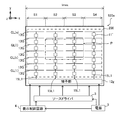
- a plurality of gate drivers 11 are connected to the gate lines 13G of GL (1) to GL (n) in the display area.
- the gate drivers 11 connected to the same gate line 13G are synchronized, and one gate line 13G is simultaneously driven by a set signal output from these gate drivers 11.
- each of the gate drivers 11 is connected to the gate lines 13G at substantially equal intervals so that the load for driving one gate line 13G is substantially equal.
- a wiring in which the source terminal of TFT-B, the drain terminal of TFT-A, the source terminal of TFT-C, and the gate terminal of TFT-F are connected is referred to as netA.
- a wiring connecting the gate terminal of the TFT-C, the source terminal of the TFT-G, the drain terminal of the TFT-H, the source terminal of the TFT-I, and the source terminal of the TFT-J is denoted by netB. Called.
- the clock signals supplied to the TFT-D, TFT-F, TFT-H, and TFT-G are supplied to the TFTs of the gate drivers 11 in adjacent rows. They are arranged so as to be opposite in phase to the clock signals supplied to each. That is, TFT-D, TFT-F, TFT-H, and TFT-G are arranged in a pixel region that is shifted in the horizontal direction from the pixel region in which these TFTs in adjacent rows are formed.
- the TFT-G in the upper pixel region is formed in the pixel region 216G, while the TFT-G in the lower pixel region is formed in the pixel region 205B.
- the clock signal (CKA) is supplied to the TFT-D in the upper pixel area, and the clock signal (CKA) having a phase opposite to that of the clock signal (CKA) is supplied to the TFT-D in the lower pixel area.
- CKB is supplied.
- clock signals (CKA or CKB) having opposite phases are supplied to the upper pixel region and the lower pixel region.
- Drain terminal 15Sd 1 in the contact portion CH3, it is connected to the gate line 13G of GL (n-2), in the contact portion CH4, is connected to the gate terminal 13 g.
- the source terminal 15Sd 2 of B2 side is connected to the wiring 13N in the contact portion CH2.
- the TFT-B is connected to the netA and receives the set signal (S) via the gate line 13G of GL (n-2).
- the source wiring layer 15 forms a source-drain terminal 15sd (including 15sd 1 and 15sd 2 ) of the TFT-C and a wiring 15L1.
- drain terminal 15Sd 1 and the wiring 13Na of C1 side is connected.
- the TFT-C is connected to netA by a wiring 13Na and connected to netB by a wiring 13Nb.
- the TFT-C is supplied with a power supply voltage signal (VSS) via the wiring 15L1.
- VSS power supply voltage signal
- source terminal 15Sd 2 of G2 side of TFT-G are connected to the wiring 13N. Further, the gate terminal 13g of the TFT-G, in the contact portion CH4, is connected to the drain terminal 15Sd 1 and the wiring 15L1 of G1 side. Thereby, the TFT-G is connected to the netB, and the clock signal (CKB) is supplied through the wiring 15L1.
- the connection portion 15Lc has substantially the same width as the wiring 13N, is formed to extend from the electrode 15c to the contact portion CH2, and is connected to the wiring 13N at the contact portion CH2. Further, the wiring 15L2 is formed to extend from the end of the connection portion 15Lc on the contact portion CH2 side to the vicinity of the contact portion CH1. In the present embodiment, the wiring 15L2 is formed so that the aperture ratio of the pixel region where the capacitor Cbst is formed and the aperture ratio of other pixel regions are matched. In the contact portion CH2, the electrode 15c is connected to the wiring 13N by the connection portion 15Lc. Thereby, the capacitor Cbst is connected to netA.
- FIG. 8F is an enlarged plan view of the pixel regions 201B and 202R shown in FIG. 5A.
- the illustration of the light shielding region BM is omitted.
- the source terminal 15s and the drain terminal 15d of the TFT-D and the wiring 15L1 are formed by the source wiring layer 15 as in the pixel areas 204G and 204B described above.
- the drain terminal 15d is connected to the GL (n ⁇ 1) gate line 13G at the contact portion CH5 in the pixel region 201B.
- the TFT-D is supplied with the power supply voltage signal (VSS) and the clock signal (CKA) via the wiring 15L1 in the pixel regions 201B and 202R, and the timing at which the clock signal (CKA) becomes H level is set via the contact portion CH5.
- An L-level potential (VSS) is output to the gate line 13G of GL (n ⁇ 1).
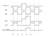
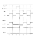
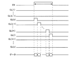
- FIG. 9 is a timing chart when the gate driver 11 scans the gate line 13G.
- a period from t3 to t4 is a period in which the GL (n) gate line 13G is selected.
- a clock signal (CKA) and a clock signal (CKB) supplied from the display control circuit 4 and whose phases are inverted every horizontal scanning period are input to the gate driver 11 via terminals 116 to 119.
- a reset signal (CLR) that is at a H (High) level for a certain period every vertical scanning period is sent from the display control circuit 4 to the gate driver 11 via the terminals 113 to 115. Entered.
- the reset signal (CLR) is input, the netA, netB, and gate line 13G transition to the L (Low) level.
- an L level clock signal (CKA) is input to the terminals 116 and 117, and an H level clock signal (CKB) is input to the terminals 118 and 119.
- CKA L level clock signal
- CKB H level clock signal
- TFT-G is turned on and TFT-H is turned off, so that netB is charged to the H level.
- TFT-C and TFT-D are turned on and TFT-F is turned off, netA is charged to the L level power supply voltage (VSS), and the L level potential is output from the terminal 120.
- VSS L level power supply voltage
- the clock signal (CKA) becomes L level and the clock signal (CKB) becomes H level, and the set signal (S) is input to the terminals 111 and 112 via the gate line 13G of GL (n ⁇ 1). .
- the TFT-B is turned on and the netA is charged to the H level.
- TFT-J is turned on
- TFT-G is turned on
- TFT-H is turned off
- netB is maintained at the L level.
- TFT-C and TFT-F are turned off, the potential of netA is maintained without being lowered.
- an L level potential is output from the terminal 120.
- the TFT-F is turned on and the TFT-D is turned off. Since the capacitor Cbst is provided between the netA and the terminal 120, the netA is charged to a potential higher than the H level of the clock signal (CKA) as the potential of the terminal 116 of the TFT-F increases. During this time, TFT-G and TFT-J are turned off and TFT-H is turned on, so that the potential of netB is maintained at the L level. Since the TFT-C is in an off state, the potential of netA does not drop, and the H level potential of the clock signal (CKA) is output from the terminal 120. As a result, the gate line 13G of GL (n) connected to the terminal 120 is charged to H level and selected, and the set signal (S) is output to the terminals 111 and 112 of GL (n + 1). .
- the gate line 13G is selected.
- the liquid crystal display device 1 sequentially scans the gate lines 13G by a plurality of gate drivers 11 connected to the respective gate lines 13G, and supplies a data signal to each source line 15S by the source driver 3, whereby an image is displayed on the display panel 2. Is displayed.
- a plurality of gate drivers 11 for driving one gate line 13G are formed between the gate lines 13G in the display region. Therefore, even when the length of the gate line 13G is determined according to the width of the outer shape of the display panel 2, each gate line 13G is sequentially selected by the set signal output from the gate driver 11 in the display area. Is done.
- control signals such as a clock signal and a power supply voltage signal supplied to each gate driver 11 are input from the one side of the display panel 2 where the source driver 3 is provided. Therefore, the frame area on the other three sides where the source driver 3 is not provided can be narrowed, and the design of the outer shape of the display panel 2 is not limited by the arrangement of the gate driver 11, and the degree of design freedom is increased. Can be improved.
- FIG. 10 is a top view showing a schematic configuration of the active matrix substrate in the present embodiment.
- the same reference numerals as those in the first embodiment are assigned to the same configurations as those in the first embodiment.
- the active matrix substrate 120a according to the present embodiment has a side opposite to the source driver 3 in the side parallel to the extending direction (X-axis direction) of the gate line 13G in the active matrix substrate 120a.
- the sides are formed in an uneven shape.
- the gate line 13G group is arranged substantially in parallel in the Y axis direction at regular intervals in each column.
- gate lines 13G of GL (1) to GL (n + a) rows are arranged.
- gate lines 13G of G (1) to G (n) rows are arranged.
- a group of source lines 15S parallel to the Y axis is formed on the active matrix substrate 120a so as to intersect with the group of gate lines 13G, and a frame on the source driver 3 side.
- a terminal portion 12s is formed in the region.
- FIG. 11 is a diagram illustrating drive timing of the active matrix substrate 120a.
- the gate driver groups 11_s1 and 11_s3 in the columns S1 and S3 sequentially drive the gate lines 13G from the GL (1) to GL (n + a) rows according to the control signals, and output set signals.
- the gate driver groups 11_s2 and 11_s4 in the columns S2 and S4 sequentially drive the gate lines 13G from the GL (1) to GL (n) rows according to the control signals, and output set signals.
- the scans of the columns S2 and S4 are finished at the timing from the start t0 to t1, and the scans of the rows S1 and S3 are finished at the timing t2.
- the gate line 13G having a length corresponding to the width of the concavo-convex portion is formed on the active matrix substrate 120a, and the gate line 13G By forming the gate driver 11 between them, the display can be controlled for each display region corresponding to the width of the uneven portion. Further, the scanning time of the gate lines 13G in the columns (S2, S4) in which the concave portions are formed is shorter than the scanning time of the gate lines 13G in the columns (S1, S3) in which the convex portions are formed.
- the data signal whose signal amplitude is minimized is output until the scanning of the column in which the convex portion is formed is completed. Therefore, it is possible to reduce the power consumption for driving the source line 15S in the column in which the recess is formed.
- FIG. 12A is a top view showing a schematic configuration of the active matrix substrate in the present embodiment.
- symbol as 1st Embodiment is attached
- a configuration different from the first embodiment will be described.
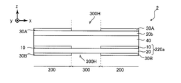
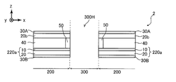
- a non-display area 300 is formed in a display area 200 indicated by a broken line.
- FIG. 12B is a diagram showing a cross section of the display panel 2 taken along the line II shown in FIG. 12A.
- the element layer 10 including the gate wiring layer 13, the source wiring layer 15, the semiconductor layer 14, and the like is formed in the display region 200 on the substrate 20 of the active matrix substrate 220a.
- the element layer 10 is not formed in the non-display area 300.
- the liquid crystal layer 40 between the active matrix substrate 20 a and the counter substrate 20 b is formed in the non-display area 300 and the display area 200.
- the polarizing plate 30A on the counter substrate 20b side and the polarizing plate 30B on the active matrix substrate 20a side are formed in the display area 200, and a hole 300H is formed in the non-display area 300 portion.
- the hole 300H is not formed in the portion of the non-display region 300 in the substrate 20 and the counter substrate 20b, and the element layer 10 and the polarization are not formed in the portion of the non-display region 300.
- the plates 30A and 30B are not formed.
- the source line 15S formed in the columns S2 and S4 and routed to the frame region 301 is formed. Therefore, the source line 15S formed in the region S31 and the source line 15S in the region S32 are not connected. Therefore, a data signal is supplied to the region S32 from the source driver 3 side along the scanning direction of the gate line 13G, but the region S31 is supplied from the frame region 301 side via the source lines 15S of the columns S2 and S4. A data signal is provided. That is, in the region S31, since the scanning direction of the gate line 13G is opposite to the scanning direction of the other regions, data is written in the order of GL (n + a) to GL (n).
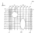
- the active matrix substrate 320a in this embodiment has a non-display area 300 formed in the display area 200, as in the third embodiment.
- a gate line 13G group having a length substantially the same as the width of the column is formed, and a gate driver 11 is formed between the gate lines 13G in the columns S1 and S4.
- each row from GL (k + 1) to GL (n) in which the non-display region 300 is formed has a gate line 13G having a length substantially the same as the width of the column S2. Yes.
- the pixel region 250 is a pixel region where the gate driver 11 is not formed.
- a bypass wiring 15 ⁇ / b> SL made of the source wiring layer 15 is formed substantially in parallel with the source line 15 ⁇ / b> S between the source lines 15 ⁇ / b> S constituting the pixel region 250.
- a bypass wiring 13n connected to the bypass wiring 15SL via the contact portion CH2 is formed substantially parallel to the gate line 13G.
- the bypass wiring 13n includes the gate wiring layer 13, and the contact portion CH2 is formed in the same manner as in FIG. 7D of the first embodiment.
- the detour wiring 13n is formed up to the source line 15S formed in the pixel region 251 of the column S3 shown in FIG.
- the display control circuit 4 is similar to the above in the case of the seal material vicinity region S1, for the gate driver 11 in the seal material vicinity region S1, S2.
- a control signal for driving the gate line 13G of S2 at 60 Hz is input through the terminal portion 12g.
- a control signal for driving the gate line 13G in the region S3 at 1 Hz is input to the gate driver 11 in the region S3 via the terminal portion 12g.
- the region near the two sides parallel to the Y axis in the display region 200 is described as an example of the region near the sealing material.
- the two sides parallel to the X axis in the display region 200 are described. It may be a nearby region or a region near the four sides of the display region 200.
- FIG. 20 is a diagram illustrating an example of an equivalent circuit of the gate driver 11 ′.
- the gate driver 11 ' is formed between the gate lines 13G of GL (n-1) and GL (n).
- the gate driver 11 ′ receives the set signal (S) from the gate driver 11 ′ (previous stage gate driver) that scans the gate line 13G of GL (n ⁇ 1), and the gate line of GL (n) according to the control signal. 13G is driven and a set signal (S) is output to the gate driver 11 ′ (next stage gate driver) that drives the gate line 13G of GL (n + 1).
- the gate driver 11 ′ has TFT-A to TFT-M switching elements composed of TFTs, a capacitor Cbst, terminals 111 to 124, and a low-level power supply voltage signal (VSS). Input terminal group. That is, the gate driver 11 'includes TFT-K, TFT-L, TFT-M, and terminals 121 to 124 in addition to the switching element of the gate driver 11 of the first embodiment shown in FIG.
- the H level potential of the clock signal (CKA) is output from the terminal 120 to the gate line 13G of GL (n).
- the netC H-level potential is input from the terminal 124 to the terminals 111 and 112 of the next-stage gate driver 11 ′ as the set signal (S) of the next-stage gate driver 11 ′.
- the netC H level potential is output from the terminal 124 to the terminal 123 of the preceding gate driver 11 ′ as a signal (R) of the preceding gate driver 11 ′.
- FIG. 21B is a timing chart showing scanning of the gate line 13G when the row selection signal (EN) indicating VSS (L level) is input to the gate driver 11 '.
- the description up to time t2 is omitted because it is the same as FIG. 21A.
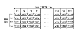
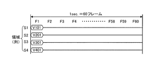
- FIG. 23A is a diagram illustrating data of each frame to be written in each area of columns S1 to S4 in display area 200.
- data of V101, V102... V160 is written for each frame of F1 to F60.
- data of V201, V202... V260 are written for each frame of F1 to F60.
- data of V301, V302... V360 are written for each frame of F1 to F60.
- data of V401, V402... V460 is written for each frame of F1 to F60.
- each gate driver 11 ′ in the columns S1 to S4 scans the gate line 13G in each column at a driving frequency of 60 Hz in accordance with the clock signal (CKA, CKB), and as shown in FIG. ) To GL (n), the gate line 13G is driven.
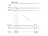
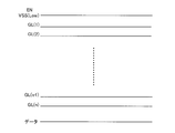
- FIG. 24B is a diagram showing the drive timing of the first frame.
- a row selection signal (EN) indicating VDD (H level) is input from the display control circuit 4 to the gate driver 11 ′ in each column.
- clock signals (CKA, CKB) are supplied to the gate drivers 11 ′ so that the gate lines 13 ⁇ / b> G in each column are driven at a driving frequency of 60 Hz.
- the data signal of the first frame shown in FIG. 24A is input from the source driver 3 to the source line 15S (see FIG. 22) formed in each column region at a driving frequency of 60 Hz.
- FIG. 24B one frame output to the source line 15S (see FIGS. 22A and 22B) in each column at the timing when the gate lines 13G of GL (1) to GL (n) are sequentially driven.
- the data of the eye data signal is written into the pixel area.
- the display control circuit 4 From the second frame to the 60th frame, the display control circuit 4 outputs a row selection signal (EN) indicating VSS (L level) to the gate driver 11 ′ in each column, and the source driver 3 determines the potential of the common electrode. Is output to the source line 15S (see FIGS. 22A and 22B).
- the gate lines 13G of GL (1) to GL (n) in each column are not driven, and the data signal output to the source line 15S (see FIGS. 22A and 22B) in each column. No data is written.
- the gate line 13G is driven only for the first frame, and the driving of the gate line 13G is stopped for 2 to 60 frames, thereby saving power. .
- the display control circuit 4 stops the supply of the clock signals (CKA, CKB) during the 2nd to 60th frames. It may be. With this configuration, power consumption can be further reduced.
- FIG. 26 is a diagram illustrating data of each frame to be written in each area of columns S1 to S4 in display area 200.
- control is performed so that data is written to the areas of the columns S1 and S4 only for the first frame and data is not written for the second to 60th frames. To do.
- the region P displays a moving image and displays a still image in a region other than the region P. Therefore, the source driver 3 continues until the first frame scan of the gate line 13G in the columns S2 and S3 is completed.
- a data signal indicating V201 and V301 to be displayed in each area of columns S2 and S3 is output to source line 15S (see FIGS. 22A and 22B) in columns S2 and S3.
- the display control circuit 4 inputs a row selection signal (EN) indicating VDD (H level) to the gate driver 11 ′ in the columns S1 to S4 so as to drive the gate line 13G at a driving frequency of 60 Hz.
- EN row selection signal
- CKA clock signals
- FIG. 23B data (V101 to V401) for each column in the first frame is written to the display area 200 at the timing when the gate lines 13G in each column are sequentially driven.
- the display control circuit 4 supplies a row selection signal (EN) indicating VSS (L level) to the gate drivers 11 'in the columns S1 and S4 after the second frame.
- the row selection signal (EN) indicating VSS (L level) is supplied during the scanning period of the gate line 13G of GL (1) to GL (k ⁇ 1).
- a row selection signal (EN) indicating VDD (H level) is supplied in the scanning period of the gate line 13G from GL (k) to GL (l).
- a row selection signal (EN) indicating VSS (L level) is supplied during the scanning period of the gate line 13G of GL (l + 1) to GL (n).
- the regions of the column S2 and the column S3 are row-selected for the scanning period of the gate lines 13G of GL (k) to GL (l) for each frame. Data is written into the region P at the timing when the signal (EN) becomes H level and the gate lines 13G of GL (k) to GL (l) are sequentially driven.
- the regions of the column S1 and the column S4 have the row selection signal (EN) while the gate lines 13G of GL (1) to GL (n) are scanned. ) Becomes L level, the gate lines 13G in the columns S1 and S4 are not driven, and data is not written.
- the active matrix substrate 620a has terminal portions 12sa and 12sb for supplying data signals.
- the terminal portions 12sa and 12sb are provided on two sides substantially parallel to the extending direction (x-axis direction) of the gate line 13G in the frame region.
- a source driver 3a is provided outside the active matrix substrate 620a on the side where the terminal portion 12sa is provided.
- the terminal portion 12sa is connected to the source driver 3a.
- a source driver 3b is provided outside the active matrix substrate 620a on the side where the terminal portion 12sb is provided.
- the terminal portion 12sb is connected to the source driver 3b.
- the source driver 3a and the source driver 3b simultaneously output the same data signal to the terminal portions 12sa and 12sb, respectively.
- the terminal portion 12g is not shown, but the terminal portion 12g is provided in the frame area where the terminal portion 12sa is provided.
- the power supply 5 (see FIG. 14 and the like) is not shown, but the power supply 5 is provided on the side where the terminal portion 12g is provided, as in the third embodiment.
- the active matrix substrate 620a, the display control circuit 4, and the source drivers 3a and 3b are supplied with a power supply voltage signal from the power supply 5.
- the active matrix substrate 620a has non-display areas 300a and 300b between the gate driver groups 11A and 11B, and a non-display area 300c between the gate driver groups 11B and 11C.
- the gate line 13G and the source line 15S intersecting in the non-display areas 300a, 300b, and 300c are divided in the non-display areas 300a, 300b, and 300c.
- the portion of the source line 15S where the non-display areas 300a, 300b, and 300c are not arranged is extended from the terminal portion 12sa to the terminal portion 12sb and connected to the terminal portion 12sa and the terminal portion 12sb. Therefore, the data signal output from the source driver 3a is supplied to the source line 15S in the portion where the non-display regions 300a, 300b, and 300c are not disposed through the terminal portion 12sa and is output from the source driver 3b. A data signal is supplied via the terminal portion 12sb.
- FIG. 28B shows a schematic diagram in which a portion where the non-display areas 300a and 300b in FIG. 28A are arranged is enlarged.
- the source line 15S arranged in the x-axis direction width R1 of the non-display area 300a and the non-display area 300b in the x-axis direction width R2 There is a break near the boundary between 300a and 300b.
- the source line 15S arranged on the terminal part 12sa side is supplied with a data signal via the terminal part 12sa and the source line 15S arranged on the terminal part 12sb side.
- the line 15S is supplied with a data signal via the terminal portion 12sb.
- the gate lines 13G of GL (k-3) to GL (k-1) on the right side (x-axis positive direction side) divided in the non-display area 300a are GL (k-3) to GL in the gate driver group 11B. It is driven by a gate driver 11 that drives GL (k ⁇ 1).
- the gate lines 13G of GL (k-10) to GL (k-5) on the left side (x-axis negative direction side) divided in the non-display area 300b are GL (k-10) to GL in the gate driver group 11A. It is driven by a gate driver 11 that drives GL (k-5).
- the gate lines 13G of GL (k-10) to GL (k-5) on the right side (x-axis positive direction side) divided in the non-display area 300b are GL (k-10) to GL in the gate driver group 11B. It is driven by a gate driver 11 that drives GL (k-5).
- the portion of the source line 15S where the non-display area is not arranged may be configured such that a data signal is supplied from either one of the source drivers 3a and 3b.
- the other source driver stops outputting the data signal to the source line 15S in the portion where the non-display area is not arranged.
- the source line 15S in the portion where the non-display area is not disposed may be configured to be connected to either the terminal portion 12sa or the terminal portion 12sb and not connected to the other.
- the terminal portion 12sb is disposed in the frame region on the short side of the two substantially parallel sides of the active matrix substrate 621a, and the terminal portion 12sa is disposed in the frame region on the long side. Yes.
- the terminal portion 12sb is connected to the source line 15S formed in the region R30 having substantially the same width as the short side of the active matrix substrate 621a.
- the terminal portion 12sa is connected to the source line 15S formed in the regions R31 and R32 excluding the region R30 in the active matrix substrate 621a.
- the terminal part 12g is provided in the frame area
- the terminal portion 12sa is outside the active matrix substrate 621a and is provided on the side where the terminal portion 12sa is arranged, as in FIG. 28A described above. It is connected to the driver 3a.
- the terminal portion 12sb is connected to the source driver 3b provided outside the active matrix substrate 621a and on the side where the terminal portion 12sb is disposed.
- the terminal unit 12sa supplies the data signal output from the source driver 3a to the source line 15S formed in the regions R31 and R32.
- the terminal unit 12sb supplies the data signal output from the source driver 3b to the region R30. This is supplied to the formed source line 15S.
- the outer shape of the active matrix substrate 20a of the first embodiment described above has an arc shape at the left and right upper end portions, and the widths of the other portions excluding the arc shape portion are substantially equal. Yes.
- the display area formed on the active matrix substrate 20a has the same shape as the outer shape.
- an example of a method for manufacturing such an active matrix substrate 20a will be described.
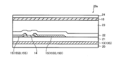
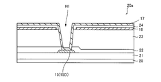
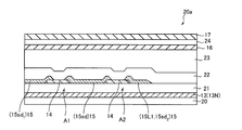
- a gate wiring layer 13, a gate insulating film 21, a semiconductor layer 14, a source wiring layer 15, a protective layer 22, a protective layer 23, and a shield layer 16 are provided on a substantially rectangular substrate 20, as shown in FIGS. 7A to 7D.
- the interlayer insulating layer 24 and the pixel electrode 17 are sequentially formed to form an active matrix substrate (first active matrix substrate) having a substantially rectangular display region.
- the first active matrix substrate has a plurality of gate lines 13G having substantially the same length and arranged at regular intervals, and arranged at regular intervals so as to intersect with the gate lines 13G.
- the plurality of source lines 15S thus formed are formed, and each layer necessary for display is formed.
- each layer formed on the substrate 20 is etched into a shape similar to the outer shape of the active matrix substrate 20a shown in FIG. That is, a part of each layer formed on the first active matrix substrate is removed so that a part of the gate lines 13G is shorter than the maximum length of the display region in the extending direction of the gate lines 13G. Then, after all the layers on the first active matrix substrate are etched, the substrate 20 is processed into a predetermined shape.
- a resist is applied to the substrate 20, and the substrate 20 is etched with an etching solution containing hydrofluoric acid or ammonium hydrogen fluoride and / or ammonium phosphate using the predetermined mask pattern. Thereby, the substrate 20 is etched into a predetermined shape, and an active matrix substrate 20a (second active matrix substrate) illustrated in FIG. 2 is formed.
- the cutting of the substrate 20 is not limited to the etching method using hydrofluoric acid or the like, and may be cut using a diamond cutter or may be cut using a grinder.
- the first active matrix substrate After the first active matrix substrate is generated, the first active matrix substrate, the first active matrix substrate bonded to the counter substrate, or the liquid crystal layer between the first active matrix substrate and the counter substrate You may make it perform the cutting
- a resist may be applied and etched using an etchant containing hydrofluoric acid or ammonium hydrogen fluoride and / or ammonium phosphate using the predetermined mask pattern.
- the first manufacturing method after all the layers are formed on the substantially rectangular substrate 20 to generate the first active matrix substrate having the substantially rectangular display region, at least a part of the gate lines 13G is gated. A part of the first active matrix substrate is removed so as to be shorter than the maximum length of the width of the display region in the extending direction of the line 13G, thereby generating a second active matrix substrate.
- the second manufacturing method described below each time a layer is formed on the substrate 20, a part of the layer is removed to generate a second active matrix substrate.
- the second manufacturing method will be described.
- FIG. 30A is a top view schematically showing a state in which the gate wiring layer 13 is formed on the substrate 20.
- a plurality of gate lines 13G having substantially the same length are formed at regular intervals substantially in parallel.
- a resist is applied on the gate wiring layer 13, and the gate wiring layer 13 is etched using a predetermined mask pattern.
- FIG. 30B the part of the gate line 13G formed outside the shape P corresponding to the predetermined mask pattern in FIG. 30A is removed.
- the arc-shaped portion of the gate line 13G is shorter than the other gate lines 13G.
- a gate insulating film 21 is formed on the gate wiring layer 13
- a resist is applied on the gate insulating film 21, and gate insulation is performed using a predetermined mask pattern.
- the film 21 is etched. Thereby, the gate insulating film 21 formed outside the shape P corresponding to the predetermined mask pattern is removed (not shown).
- the source wiring layer 15 is formed on the semiconductor layer 14. Thereby, as shown in FIG. 30C, source lines 15S having substantially the same length are formed at regular intervals so as to intersect with the gate line 13G. After the formation of the source wiring layer 15, a resist is applied on the source wiring layer 15, and the source wiring layer 15 is etched using a predetermined mask pattern. Thus, as shown in FIG. 30D, the source wiring layer 15 formed outside the shape P corresponding to the predetermined mask pattern in FIG. 30C is removed.
- a protective layer 22, a protective layer 23, a shield layer 16, an interlayer insulating layer 24, a pixel electrode 17, and contact holes H1 and H2 are sequentially formed (illustrated). (Omitted).
- a resist is applied and etched with a predetermined mask pattern.
- each layer on the substrate 20 is etched into a shape similar to the outer shape of the active matrix substrate 20a shown in FIG.
- a resist is applied to the substrate 20 and the substrate 20 is etched with a predetermined mask pattern, thereby finally generating a second active matrix substrate.
- the active matrix substrate 720a has gate lines 13G of GL (1) to GL (n).
- the active matrix substrate 720a includes gate driver groups 11 ⁇ and 11 ⁇ .
- the gate driver group 11 ⁇ includes a gate driver 11 provided for each of the gate lines 13G of GL (1) to GL (n).
- the gate driver group 11 ⁇ includes the gate drivers 11 provided for the gate lines 13G of GL (k + 1) to GL (n).
- the gate drivers 11 in the gate driver groups 11 ⁇ and 11 ⁇ are connected by the wiring 15L1 as in the first embodiment.
- a gate line 13G is formed between a portion where the gate driver group 11 ⁇ is formed and a portion where the gate driver group 11 ⁇ is not formed. Cut along.
- the active matrix substrate 720a is cut at a position based on the cutting line H between the gate lines 13G of GL (k) and GL (k + 1).
- two active matrix substrates 721a and 722a are generated as shown in FIG. 31B.
- the active matrix substrates 721a and 722a are etched using a predetermined mask pattern, thereby obtaining the same shape as the active matrix substrate 20a illustrated in FIG.
- the active matrix substrates 721a and 722a (see FIGS. 31C and 31D) having the second active matrix substrate are generated.
- a terminal portion 12g is provided on the side of the active matrix substrate 722a where the gate line 13G of the GL (1) is disposed in the frame region.
- the gate driver group 11 ⁇ and the terminal portion 12g are connected.
- the start pulse signal output from the display control circuit 4 is supplied to the gate driver 11 that drives the gate line 13G of the GL (1) of the gate driver group 11 ⁇ via the terminal portion 12g.
- a control signal (clock signal or the like) output from the display control circuit 4 is supplied to the gate driver group 11 ⁇ via the terminal portion 12g.
- the gate lines 13G are sequentially driven in the order of GL (1) to GL (k).
- a terminal portion 12g is provided on the side where the GL (1) gate line 13G is arranged in the frame region, and the gate The driver group 11 ⁇ and the terminal portion 12g are connected.
- the start pulse signal from the display control circuit 4 is supplied to the gate driver 11 that drives the gate line 13G of GL (1) through the terminal portion 12g.
- the gate line 13G is driven in the order of GL (1) to GL (n) in accordance with a control signal (clock signal or the like) from the display control circuit 4.
- the gate driver group 11 ⁇ is not driven because no control signal is supplied.
- Application example 2 In the application example 1 described above, the example in which the active matrix substrate 720a is cut in substantially parallel to the extending direction of the gate line 13G has been described. However, the active matrix substrate 720a is cut in a direction substantially orthogonal to the extending direction of the gate line 13G. An active matrix substrate may be generated.
- the active matrix substrate 720a is cut up and down or left and right to generate two active matrix substrates.
- the first active matrix substrate is cut up and down and left and right to form four active matrix substrates.
- a second active matrix substrate may be generated.
- FIG. 33A is a top view schematically showing a schematic configuration of the first active matrix substrate according to this application example.
- the source line 15S is not shown.
- alternate long and short dash lines H1 and H2 indicate reference positions for cutting, and are hereinafter referred to as cutting lines H1 and H2.
- an active matrix substrate 820a which is an example of a first active matrix substrate, includes gate driver groups 11 ⁇ L and 11 ⁇ L in left and right regions separated by a cutting line H1 substantially orthogonal to the extending direction of the gate line 13G.
- Gate driver groups 11 ⁇ R and 11 ⁇ R are formed.
- the gate driver groups 11 ⁇ L and 11 ⁇ R include gate drivers 11 provided for the gate lines 13G of GL (1) to GL (n).
- the gate driver groups 11 ⁇ L and 11 ⁇ R include gate drivers 11 provided for the gate lines GL (n) to GL (k + 1).
- the active matrix substrate 820a includes a gate driver (first gate line driving circuit) provided for each gate line 13G and a gate driver (second gate driver) provided for each of some adjacent gate lines 13G.
- a gate driver first gate line driving circuit
- second gate driver second gate driver
- a plurality of pairs 11 ⁇ L and 11 ⁇ L, 11 ⁇ R and 11 ⁇ R are formed.
- the active matrix substrates 821a, 822a, 823a, and 824a are generated by cutting the active matrix substrate 820a with reference to the positions of the cutting lines H1 and H2, as shown in FIG. 33B. That is, in the active matrix substrate 820a, the pair of the first gate line driving circuit and the second gate line driving circuit is cut along the source line 15S (not shown), thereby forming the second active matrix substrate. As an example, four active matrix substrates 821a, 822a, 823a, and 824a are generated.
- the active matrix substrate 823a is provided with a part of the gate driver group 11 ⁇ L
- the active matrix substrate 824a is provided with a part of the gate driver group 11 ⁇ R.
- Each of the gate driver groups 11 ⁇ L and 11 ⁇ R in the active matrix substrates 823a and 824a includes the gate driver 11 provided for the gate lines 13G of GL (1) to GL (k).
- the active matrix substrate 823a and the active matrix substrate 824a are connected to the gate driver groups 11 ⁇ L and 11 ⁇ R, respectively, in the same manner as the active matrix substrate 722a shown in FIG. 31D described above.
- a terminal portion 12g is provided.
- the gate lines 13G are driven in the order of GL (1) to GL (k) by the gate driver groups 11 ⁇ L and 11 ⁇ R.
- first active matrix substrate a plurality of active matrix substrates (first active matrix substrates smaller in size than the first active matrix substrate). 2 active matrix substrates). Therefore, the production line is made more efficient and the production cost can be reduced as compared with the case where an active matrix substrate is produced for each display size (number of pixels).
- the pixels in the cut portion are lost by cutting the first active matrix substrate. Therefore, it is preferable to design the first active matrix substrate in consideration of the number of pixels lost by the cut portion. For example, when the active matrix substrate 820a illustrated in FIG. 33A corresponds to a display having the number of pixels “8K4K” (7680 ⁇ 4320), the number of pixels of the active matrix substrate 820a is set to (8K + 100 pixels) ⁇ (4K + 50 pixels) or the like. As described above, the number of pixels is increased from “8K4K” (7680 ⁇ 4320).
- a wiring pattern of the terminal portion 12s for supplying the data signal from the source driver 3 to the source line 15S is formed.
- the wiring pattern of the terminal portion 12s is also cut, and the pixel that cannot supply the data signal in the cut active matrix substrate. May occur.
- a first active matrix substrate is generated so that a pixel to which no data signal is supplied does not occur in a cut active matrix substrate.
- FIG. 34A is a schematic view illustrating a part of the first active matrix substrate according to this application example.
- the terminal groups 12s_2 and 12s_5 including are formed.
- terminal portions 12s are connected to, for example, 360 source lines 15S.
- the terminal groups 12s_2 and 12s_5 include 14 terminal portions 12s.
- the active matrix substrate 920a is provided with one or a plurality of gate drivers 11 for each divided gate line 13G.
- Gate driver groups 11a and 11b are connected to the gate line 13G intersecting the source line 15S connected to the terminal portion 12s_1, the terminal group 12s_2, and the terminal portion 12s_3.
- the gate driver group 11c is connected to the gate line 13G that intersects the source line 15S connected to the terminal portion 12s_4.
- Gate driver groups 11d and 11e are connected to the gate line 13G intersecting the source line 15S connected to the terminal group 12s_5 and the terminal portion 12s_6.
- a gate driver group 11f is connected to the gate line 13G that intersects the source line 15S connected to the terminal portion 12s_7.
- the active matrix substrate 920a When an active matrix substrate for display having a first number of pixels (for example, 3840 ⁇ 1080) is generated from the active matrix substrate 920a, the active matrix substrate 920a is cut at the position of the pixel region between H13 and H10 in FIG. 34A. To do. Thereby, the pixel region between H13 and H10, that is, the pixel region driven by the gate driver group 11f is cut, and driven by the 32 terminal portions 12s (12s_1 to 12s_6) and the gate driver groups 11a to 11e. An active matrix substrate is generated.
- a first number of pixels for example, 3840 ⁇ 1080
- the gate lines 13G is formed.
- a second active matrix substrate shorter than the maximum length of the display area in the extending direction of the gate line 13G is generated.
- a predetermined shape is obtained as in the first manufacturing method described above.
- the second active matrix substrate may be generated by cutting so that
- the case where the number of source lines 15S connected to one terminal portion 12s is the same has been described. Since the same source driver can be used for each terminal portion 12 s because the number of outputs of one terminal portion 12 s is the same, manufacturing costs can be reduced, design efficiency can be improved, and display can be made uniform. Can do. However, the number of terminals of the terminal portion 12s_4 and the terminal portion 12s_7 can be reduced in order to minimize the pixel area that is unnecessary due to cutting. In this case, source drivers having different numbers of outputs may be prepared for the terminal portions 12s_4 and 12s_7 and the other terminal portions.
- one side parallel to the extending direction (X-axis direction) of the gate line 13G is formed in an uneven shape.
- two sides parallel to the extending direction (Y-axis direction) of the source line 15S may be formed in an uneven shape.
- portions where two sides parallel to the Y axis of the active matrix substrate 121a are formed inwardly are referred to as non-display regions 310A and 310B.
- gate lines 13G having a length substantially the same as the width in the X-axis direction of the non-display areas 310A and 310B are formed in the columns S1 and S4 where the non-display areas 310A and 310B are located. Yes.
- gate lines 13G having a length substantially the same as the width of each column are formed in the columns S2 and S3 obtained by dividing the region between the columns S1 and S4. That is, the length of each gate line 13 is shorter than the maximum length lmax of the width in the X-axis direction in the active matrix substrate 121a.
- a gate driver 11 is formed in the column S3 between the gate lines 13G in the columns S3 and S4. Accordingly, in this example, the gate driver 11 is not formed in the regions S31b and S32b of the column S1 where the non-display regions 310A and 310B are formed and the regions S31a and S32a of the column S4.
- one non-display area 300 is formed in the display area 200.
- a plurality of non-display areas 300a and 300b may be formed.
- gate lines having substantially the same length as the width in the X-axis direction of the non-display areas 300a and 300b. 13G is formed. Gate lines 13G having substantially the same length are formed in the columns S1, S3, and S5 in which the non-display areas 300a and 300b are not formed. Each gate line 13G is long enough to form at least one gate driver 11.
- the source lines 15S are formed so as to intersect with the gate lines 13G in each column.
- the terminal portion 12s for supplying the data signal from the source driver 3 to each source line 15S is arranged in a frame region where the terminal portion 12g is formed.
- the source lines 15S of the regions S31a and S31b on the frame region 301 side in the columns S2 and S4 are routed to one of the source regions 15S of the columns S1 and S3 to the frame region 301, and the regions S31a, S31, It is formed by being folded back to 31b.
- the gate driver 11 in the regions S31a and 31b is routed to the frame region 301 by the wiring 15L1 connecting the gate drivers 11 in the columns S3 and S1 and folded back to the regions S31a and 31b.
- the gate drivers 11 in the columns S3 and S1 are connected.
- a gate driver 11 is formed in the column S1 between the gate lines 13G in the columns S1 and S2.
- a gate driver 11 is formed in the column S5 between the gate lines 13G in the columns S4 and S5. Accordingly, in this example, the gate driver 11 is not formed in the regions S31b and S32b of the column S2 where the non-display regions 300a and 300b are formed and the regions S31a and S32a of the column S4.
- the source lines 15S in the regions S31a and S32a sandwiching the non-display region 300a are connected to the bypass wirings 15SL and 13b (in the pixel region of the column S3). (See FIGS. 15 and 16). Further, the source lines 15S in the regions S31b and 32b sandwiching the non-display region 300b may be connected via detour wirings 15SL and 13b (see FIGS. 15 and 16) formed in the pixel region of the column S1.
- the gate driver 11 ′ in the seventh embodiment may be used instead of the gate driver 11.
- the gate driver 11 ′ By using the gate driver 11 ′, the gate line 13 ⁇ / b> G group in the display region 200 can be driven for each row.
- an arbitrary gate line when displaying a still image, an example in which an arbitrary gate line is driven only in the first frame and driving of the arbitrary gate line is stopped in the second to 60th frames will be described. However, it may be as follows. For example, an arbitrary gate line may be driven from the first frame to the second frame, and driving of the arbitrary gate line may be stopped during the third to 60th frames. In short, it may be configured to stop driving of an arbitrary gate line in at least some frames according to the driving frequency.
- the semiconductor layer 14 of the switching element constituting the gate drivers 11 and 11 ′ is made of an oxide semiconductor.
- it may be made of polysilicon, amorphous silicon, or the like.
- the gate line 13G, the source line 15S, the gate driver 11, and the terminal portion 12g to which a control signal for the gate driver 11 is input on the substrate 20 of the active matrix substrate 20a.
- the source driver 3 and the display control circuit 4 may be formed in addition to these.
- the display panel 2 is a liquid crystal panel.
- the display panel 2 is a display panel that drives an active matrix substrate using organic EL (Electro-Luminescence) or the like. May be.
- At least a part of the gate lines 13G is shorter than the maximum length of the display area in the extending direction of the gate lines 13G.
- the example of removing a part of the active matrix substrate has been described. However, when an active matrix substrate used for a substantially rectangular display is generated, a step of removing a part of the active matrix substrate is not performed. . That is, for example, an active matrix substrate (721a and 722a in FIG. 31B) obtained by cutting the first active matrix substrate 720a illustrated in FIG. 31A with reference to the position indicated by the cutting line H may be used for the display. Alternatively, an active matrix substrate obtained by cutting the first active matrix substrate 720a shown in FIG.
- an active matrix substrate (821a to 824a in FIG. 33B) obtained by cutting the first active matrix substrate 820a shown in FIG. 33A with reference to the positions indicated by the lines H1 and H2 may be used for the display.
- a matrix substrate (921a and 922a in FIG. 34B) may be used for the display.
- the present invention can be used for a display including a display panel using liquid crystal, organic EL, or the like.
Abstract
Description
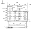
(液晶表示装置の構成)
図1は、本実施形態に係る液晶表示装置の概略構成を示した上面図である。液晶表示装置1は、表示パネル2、ソースドライバ3、表示制御回路4、及び電源5を有する。表示パネル2は、アクティブマトリクス基板20aと、対向基板20bと、これら基板に挟持された液晶層(図示略)とを有する。図1において図示を省略しているが、アクティブマトリクス基板20aの下面側と対向基板20bの上面側には、偏光板が設けられている。対向基板20bには、ブラックマトリクスと、赤(R)、緑(G)、青(B)の3色のカラーフィルタと、共通電極(いずれも図示略)が形成されている。 <First Embodiment>
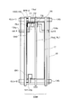
(Configuration of liquid crystal display device)
FIG. 1 is a top view showing a schematic configuration of the liquid crystal display device according to the present embodiment. The liquid
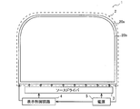
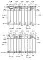
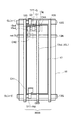
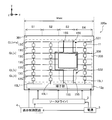
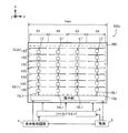
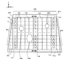
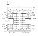
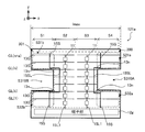
図2は、アクティブマトリクス基板20aの概略構成を示す上面図である。図2に示すように、アクティブマトリクス基板20aにおけるY軸正方向の左右の端部は、円弧状に形成されている。アクティブマトリクス基板20aにおいて、X軸方向の一端から他端までゲート線13G群が一定の間隔で略平行に形成されている。ゲート線13G群のうち、円弧状の部分に形成された一部のゲート線群13G_aは、アクティブマトリクス基板20aにおけるX軸方向の幅の最大長lmaxより短く、他のゲート線13G_b群は、最大長lmaxと略同じ長さに形成されている。 (Configuration of active matrix substrate)
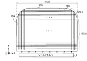
FIG. 2 is a top view showing a schematic configuration of the
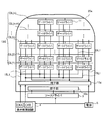
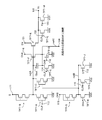
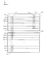
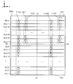
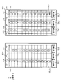
ここで、本実施形態におけるゲートドライバ11の構成について説明する。図4は、GL(n-1)とGL(n-2)のゲート線13G間に配置され、GL(n-1)のゲート線13Gを駆動する1つのゲートドライバ11の等価回路の一例を示す図である。図4に示すように、ゲートドライバ11は、スイッチング素子として薄膜トランジスタ(TFT:Thin Film Transistor)で構成されたTFT-A~TFT-Jと、キャパシタCbstと、端子111~120と、ローレベルの電源電圧信号が入力される端子群とを有する。 (Configuration of the gate driver 11)
Here, the configuration of the
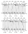
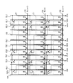
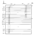
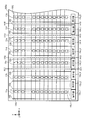
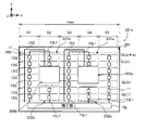
次に、表示領域におけるゲートドライバ11の各素子の配置について説明する。図5A~図5Cは、GL(n)とGL(n-1)、GL(n-1)とGL(n-2)のゲート線13G間に配置されている1つのゲートドライバ11の配置例を示す図である。図5A~図5Cでは、便宜上、GL(n)とGL(n-1)の間の画素領域211R~217Bと、GL(n-1)とGL(n-2)の間の画素領域201R~207Bとが分離されて記載されているが、実際はGL(n-1)のゲート線13Gにおいて重ね合わされ、上下の画素領域は連続している。なお、画素領域を示す符号に含まれるR、G、Bは、対向基板20bに形成されているカラーフィルタ(図示略)の色を示している。 (Overall layout of gate driver)
Next, the arrangement of each element of the
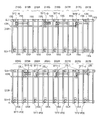
また、図5Cに示すように、上段画素領域のTFT-Hは、画素領域215G及び215Bに形成されているのに対し、下段画素領域のTFT-Hは、画素領域206R及び206Gに形成されている。上段画素領域のTFT-Gは、画素領域216Gに形成されているのに対し、下段画素領域のTFT-Gは、画素領域205Bに形成されている。このように構成することで、上段画素領域のTFT-Dにはクロック信号(CKA)が供給され、下段画素領域のTFT-Dには、クロック信号(CKA)とは逆位相となるクロック信号(CKB)が供給される。TFT-F、TFT-H、TFTについても、図5A及び図5Cに示すように上段画素領域と下段画素領域とで逆位相のクロック信号(CKA又はCKB)が供給される。 Specifically, as shown in FIG. 5A, the TFT-D in the upper pixel area is formed in the
Further, as shown in FIG. 5C, the upper pixel area TFT-H is formed in the
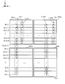
次に、TFT-Bの接続方法について説明する。図8Aは、図5Bに示した画素領域204Rを拡大した平面図である。図8Aにおいて遮光領域BMの図示は省略されている。図8Aに示すように、画素領域204Rには、上述した画素領域204Gと同様に、コンタクト部CH1においてTFT-PIXと画素電極17とが接続されている。また、ソース配線層15によって、TFT-Bのソース-ドレイン端子15sd(15sd1,15sd2含む)が形成されている。ゲート配線層13によって、TFT-Bのゲート端子13gと、GL(n-2)のゲート線13G及び配線13Nが形成されている。 (TFT-B)
Next, a method for connecting TFT-B will be described. FIG. 8A is an enlarged plan view of the
次に、TFT-Cの接続方法について説明する。図8Bは、図5Bに示した画素領域205Rを拡大した平面図である。図8Bにおいて遮光領域BMの図示は省略されている。図8Bに示すように、画素領域205Rには、上述した画素領域204G及び204Bと同様に、コンタクト部CH1においてTFT-PIXと画素電極17とが接続されている。また、ゲート配線層13により、TFT-Cのゲート端子13gと、ゲート線13G及び配線13N(13Na,13Nb)とが形成されている。ソース配線層15により、TFT-Cのソース-ドレイン端子15sd(15sd1,15sd2含む)と配線15L1とが形成されている。コンタクト部CH2において、C1側のドレイン端子15sd1と配線13Naは接続されている。TFT-Cは、配線13NaによりnetAと接続され、配線13NbによりnetBと接続される。また、TFT-Cは、配線15L1を介して電源電圧信号(VSS)が供給される。 (TFT-C)
Next, a method for connecting TFT-C will be described. FIG. 8B is an enlarged plan view of the
次に、TFT-Fの接続方法について説明する。図8Cは、図5Aに示した画素領域203Rを拡大した平面図である。図8Cにおいて遮光領域BMの図示は省略されている。図8Cに示すように、画素領域203Rには、画素領域204G及び204Bと同様に、コンタクト部CH1においてTFT-PIXと画素電極17とが接続されている。また、ゲート配線層13により、TFT-Cのゲート端子13gと、ゲート線13G及び配線13Nとが形成されている。ソース配線層15により、TFT-Fのソース端子15s及びドレイン端子15dと配線15L1とが形成されている。 (TFT-F)
Next, a method for connecting TFT-F will be described. FIG. 8C is an enlarged plan view of the
次に、TFT-Gの接続方法について説明する。図8Dは、図5Cに示した画素領域205Bを拡大した平面図である。図8Dにおいて遮光領域BMの図示は省略されている。図8Dに示すように、画素領域205Bには、画素領域204G及び204Bと同様に、コンタクト部CH1においてTFT-PIXと画素電極17とが接続されている。また、ゲート配線層13により、TFT-Gのゲート端子13gと、ゲート線13G及び配線13Nが形成されている。ソース配線層15により、TFT-Gのソース-ドレイン端子15sd(15sd1,15sd2含む)と配線15L1とが形成されている。コンタクト部CH2において、TFT-GのG2側のソース端子15sd2は配線13Nと接続されている。また、TFT-Gのゲート端子13gは、コンタクト部CH4において、G1側のドレイン端子15sd1及び配線15L1と接続されている。これにより、TFT-Gは、netBと接続され、配線15L1を介してクロック信号(CKB)が供給される。 (TFT-G)
Next, a method for connecting TFT-G will be described. FIG. 8D is an enlarged plan view of the
次に、キャパシタCbstの接続方法について説明する。図8Eは、図5Bに示した画素領域203Bを拡大した平面図である。図8Eにおいて遮光領域BMの図示は省略されている。画素領域203Bには、上述した画素領域204G及び204Bと同様に、コンタクト部CH1においてTFT-PIXと画素電極17とが接続されている。また、ゲート配線層13により、キャパシタCbstを構成する一方の電極13cと、ゲート線13G及び配線13Nとが形成されている。ソース配線層15により、キャパシタCbstの他方の電極15cと、接続部15Lcと、配線15L2とが形成されている。図8Eに示すように、接続部15Lcは、配線13Nと略同じ幅を有し、電極15cからコンタクト部CH2まで延伸されて形成され、コンタクト部CH2において配線13Nと接続されている。また、配線15L2は、接続部15Lcのコンタクト部CH2側の端部からコンタクト部CH1の近傍まで延伸されて形成されている。本実施形態では、配線15L2を形成することにより、キャパシタCbstが形成される画素領域の開口率と他の画素領域との開口率を合わせるようにしている。コンタクト部CH2において、電極15cは接続部15Lcによって配線13Nと接続されている。これにより、キャパシタCbstは、netAと接続される。 (Cbst)
Next, a method for connecting the capacitor Cbst will be described. FIG. 8E is an enlarged plan view of the
次に、TFT-D及びTFT-Eの接続方法について説明する。TFT-DとTFT-Eは、上述したTFT-Aと同様、隣接する2つの画素領域にわたってゲート端子13gが形成され、一方の画素領域に形成された配線15L1とゲート端子13gが接続されている。TFT-D及びTFT-Eは、ゲート端子に供給される信号がリセット信号(CLR)であるかクロック信号(CKA)であるかの違いであるため、以下、TFT-Dの接続方法について説明する。 (TFT-D, E)
Next, a method for connecting TFT-D and TFT-E will be described. In the TFT-D and the TFT-E, similarly to the TFT-A described above, the
次に、図4及び図9を参照しつつ、1つのゲートドライバ11の動作について説明する。図9は、ゲートドライバ11がゲート線13Gを走査する際のタイミングチャートである。図9において、t3からt4の期間がGL(n)のゲート線13Gが選択されている期間である。表示制御回路4から供給される、一水平走査期間毎に位相が反転するクロック信号(CKA)とクロック信号(CKB)とが端子116~119を介してゲートドライバ11に入力される。また、図9では図示を省略しているが、一垂直走査期間毎に一定期間H(High)レベルとなるリセット信号(CLR)が表示制御回路4から端子113~115を介してゲートドライバ11に入力される。リセット信号(CLR)が入力されると、netA、netB、ゲート線13GはL(Low)レベルに遷移する。 (Operation of the gate driver 11)
Next, the operation of one
図10は、本実施形態におけるアクティブマトリクス基板の概略構成を示す上面図である。この図において、第1実施形態と同様の構成には、第1実施形態と同じ符号を付している。以下、第1実施形態と異なる構成について説明する。本実施形態に係るアクティブマトリクス基板120aは、図10に示すように、アクティブマトリクス基板120aにおいて、ゲート線13Gの延伸方向(X軸方向)に平行な辺のうち、ソースドライバ3とは反対側の辺が凹凸形状に形成されている。そして、アクティブマトリクス基板120aにおける凹部と凸部のX軸方向の幅と略同じ長さのゲート線13G群が、その幅の各列(以下、列S1、S2、S3、S4)に形成されている。すなわち、図10の例では、各ゲート線13Gは、アクティブマトリクス基板120aにおけるゲート線13Gの延伸方向(X軸方向)の幅の最大長lmaxより短い長さに形成されている。 Second Embodiment
FIG. 10 is a top view showing a schematic configuration of the active matrix substrate in the present embodiment. In this figure, the same reference numerals as those in the first embodiment are assigned to the same configurations as those in the first embodiment. Hereinafter, a configuration different from the first embodiment will be described. As shown in FIG. 10, the
本実施形態では、表示領域内に非表示領域が形成されているアクティブマトリクス基板の例について説明する。図12Aは、本実施形態におけるアクティブマトリクス基板の概略構成を示す上面図である。図12Aにおいて、第1実施形態と同様の構成には、第1実施形態と同じ符号を付している。以下、第1実施形態と異なる構成について説明する。 <Third Embodiment>
In this embodiment, an example of an active matrix substrate in which a non-display area is formed in the display area will be described. FIG. 12A is a top view showing a schematic configuration of the active matrix substrate in the present embodiment. In FIG. 12A, the same code | symbol as 1st Embodiment is attached | subjected to the structure similar to 1st Embodiment. Hereinafter, a configuration different from the first embodiment will be described.
上述した第3実施形態では、非表示領域300が形成されていない列のソース線15Sを額縁領域301まで引き回し、非表示領域300が形成された列に折り返すことで、非表示領域300が形成された列のソースドライバ3と反対側の領域S31にソース線15Sを形成する例であった。本実施形態では、非表示領域300が形成されていない列のソース線15Sを額縁領域301まで引き回すことなく、非表示領域300が形成されている列にソース線15Sを形成する例を説明する。図14は、本実施形態におけるアクティブマトリクス基板の概略構成を示す上面図である。図14において、第1実施形態及び第3実施形態と同様の構成には、第1実施形態及び第3実施形態と同じ符号を付している。以下、第3実施形態と異なる構成について説明する。 <Fourth embodiment>
In the third embodiment described above, the
本実施形態では、表示領域の一部の領域を第1の駆動周波数で駆動し、他の領域を第1の駆動周波数より低い第2の駆動周波数で駆動させる例について説明する。以下、前述した実施形態と同様の構成については同じ符号を用い、前述した実施形態と異なる構成について説明を行う。 <Fifth Embodiment>
In this embodiment, an example in which a part of the display area is driven at the first driving frequency and the other area is driven at the second driving frequency lower than the first driving frequency will be described. Hereinafter, the same reference numerals are used for configurations similar to those in the above-described embodiment, and configurations different from those in the above-described embodiment will be described.
上述した第5実施形態の図17では、領域S1~S3のゲート線13Gは、領域の幅と略同じ長さとなるように形成されている例を説明した。図17の例では、1Hz相当で駆動される領域S1、S2と、60Hz相当で駆動される領域S3との境界が直線状であるため、その境界部分が人の目に感知されやすい。そのため、本実施形態では、駆動周波数が異なる領域の境界が非直線状となるようにゲート線13Gを形成する例を説明する。 <Sixth Embodiment>
In FIG. 17 of the fifth embodiment described above, the example in which the
上述した第6実施形態では、表示領域における列に応じて異なる駆動周波数で駆動させる例について説明した。本実施形態では、表示領域における列及び行に応じて異なる駆動周波数で駆動させる例について説明する。 <Seventh embodiment>
In the sixth embodiment described above, an example in which driving is performed at different driving frequencies according to the columns in the display area has been described. In this embodiment, an example in which driving is performed at different driving frequencies depending on columns and rows in the display area will be described.
上述した第3実施形態及び第4実施形態では、額縁領域において端子部12gが設けられた辺に端子部12sを設け、端子部12sを介してソース線15Sにデータ信号を供給する例を説明した。本実施形態では、第3実施形態及び第4実施形態と同様、表示領域内に非表示領域を有する場合において、端子部12sが設けられた辺に対向する辺にもデータ信号を供給する端子部を設け、両方の端子部からデータ信号をソース線15Sに供給する例を説明する。 <Eighth Embodiment>
In the third embodiment and the fourth embodiment described above, the example in which the
上述した第8実施形態では、非表示領域が配置されていない部分のソース線15Sは、端子部12sa及び端子部12sbを介してソースドライバ3a,3bからのデータ信号が供給される例を説明したが、非表示領域が配置されていない部分のソース線15Sは、ソースドライバ3a,3bのいずれか一方からデータ信号が供給されるように構成してもよい。この場合、他方のソースドライバは、非表示領域が配置されていない部分のソース線15Sに対するデータ信号の出力を停止する。また、非表示領域が配置されていない部分のソース線15Sは、端子部12sa又は端子部12sbのいずれか一方に接続し、他方と接続しないように構成してもよい。 <Application Example 8 of Eighth Embodiment>
In the above-described eighth embodiment, the example in which the data signals from the
上述した第8実施形態の例では、アクティブマトリクス基板620aは、略長方形の形状を有し、表示領域内に非表示領域を有する例を説明したが、例えば、図29に例示するように、台形状を有し、表示領域200内に非表示領域を有するアクティブマトリクス基板621aであってもよい。 <Application Example 8 of Eighth Embodiment>
In the above-described example of the eighth embodiment, the
上述した第1実施形態のアクティブマトリクス基板20aの外形は、図2に示すように、左右の上端部分が円弧状を有し、円弧状の部分を除く他の部分の幅が略同等となっている。このアクティブマトリクス基板20aに形成されている表示領域も外形と同様の形状を有する。以下、このようなアクティブマトリクス基板20aの製造方法の一例について説明する。 <Ninth Embodiment>
As shown in FIG. 2, the outer shape of the
まず、略長方形状の基板20上に、図7A~7Dに示すように、ゲート配線層13、ゲート絶縁膜21、半導体層14、ソース配線層15、保護層22、保護層23、シールド層16、層間絶縁層24、画素電極17の各層を順次形成して、略長方形の表示領域を有するアクティブマトリクス基板(第1のアクティブマトリクス基板)を形成する。つまり。第1のアクティブマトリクス基板には、略同じ長さを有し、一定間隔に配列された複数のゲート線13Gと、略同じ長さを有し、ゲート線13Gと交差するように一定間隔に配列された複数のソース線15Sが形成されるとともに、表示に必要な各層が形成されている。 (First manufacturing method)
First, on a substantially
まず、略長方形の基板20にゲート配線層13を形成する。図30Aは、基板20上にゲート配線層13が形成された状態を模式的に表した上面図である。ゲート配線層13の形成により、図30Aに示すように、略平行に一定の間隔で、略同じ長さの複数のゲート線13Gが形成される。ゲート配線層13の形成後、ゲート配線層13の上にレジストを塗布し、所定のマスクパターンを用いてゲート配線層13をエッチングする。これにより、図30Bに示すように、図30Aにおいて、所定のマスクパターンに対応する形状Pより外側に形成されているゲート線13Gの部分が除去される。その結果、円弧状の部分のゲート線13Gは、他のゲート線13Gより短くなる。 (Second manufacturing method)
First, the
上述した第9実施形態では、ディスプレイのサイズ(画素数)ごとに上述した製造方法を用いてアクティブマトリクス基板を生成しなければならい。そのため、複数のサイズのディスプレイに対応するアクティブマトリクス基板を製造する場合には、ディスプレイのサイズに応じて複数の製造ラインが必要となる。本応用例では、ある画素数(第1の画素数)のディスプレイに対応する第1のアクティブマトリクス基板を切断し、第1の画素数より小さい第2の画素数のディスプレイに対応する複数の第2のアクティブマトリクス基板を生成する例について説明する。 <Application Example of Ninth Embodiment>
In the ninth embodiment described above, an active matrix substrate must be generated using the manufacturing method described above for each display size (number of pixels). Therefore, when manufacturing an active matrix substrate corresponding to a plurality of sizes of displays, a plurality of production lines are required depending on the size of the display. In this application example, a first active matrix substrate corresponding to a display with a certain number of pixels (first number of pixels) is cut, and a plurality of second numbers corresponding to a display with a second number of pixels smaller than the first number of pixels is obtained. An example of generating two active matrix substrates will be described.
図31Aは、本応用例における第1のアクティブマトリクス基板の一例を示す模式図である。図31Aにおいてソース線15Sの図示は省略しているが、第1のアクティブマトリクス基板の一例であるアクティブマトリクス基板720aには、ゲート線13Gと交差するように複数のソース線15Sが形成されている。 (Application 1)
FIG. 31A is a schematic diagram illustrating an example of a first active matrix substrate in the present application example. Although illustration of the
上述した応用例1では、アクティブマトリクス基板720aを、ゲート線13Gの延伸方向と略平行に切断する例を説明したが、ゲート線13Gの延伸方向と略直交する方向に切断して複数の第2のアクティブマトリクス基板を生成してもよい。 (Application example 2)
In the application example 1 described above, the example in which the
上述した応用例1、2では、アクティブマトリクス基板720aを上下又は左右に切断して2つのアクティブマトリクス基板を生成する例を説明したが、第1のアクティブマトリクス基板を上下左右に切断して4つの第2のアクティブマトリクス基板を生成してもよい。 (Application 3)
In the application examples 1 and 2 described above, the
第1のアクティブマトリクス基板には、ソースドライバ3からのデータ信号をソース線15Sに供給する端子部12sの配線パターンが形成される。上述した応用例2のように第1のアクティブマトリクス基板をソース線15Sに沿って切断すると、端子部12sの配線パターンも切断され、切断後のアクティブマトリクス基板においてデータ信号を供給することができない画素が生じる場合がある。本応用例では、切断後のアクティブマトリクス基板において、データ信号が供給されない画素が生じないように第1のアクティブマトリクス基板を生成する例について説明する。 (Application 4)
On the first active matrix substrate, a wiring pattern of the
以上、本発明の実施の形態を説明したが、上述した実施の形態は本発明を実施するための例示に過ぎない。よって、本発明は上述した実施の形態に限定されることなく、その趣旨を逸脱しない範囲内で上述した実施の形態を適宜変形して実施することが可能である。以下、本発明の変形例について説明する。 <Modification>
While the embodiments of the present invention have been described above, the above-described embodiments are merely examples for carrying out the present invention. Therefore, the present invention is not limited to the above-described embodiment, and can be implemented by appropriately modifying the above-described embodiment without departing from the spirit thereof. Hereinafter, modifications of the present invention will be described.
Claims (18)
- 複数のゲート線を含むゲート線群と、複数のソース線を含むソース線群とが行列状に配置され、前記ゲート線と前記ソース線とに接続された画素電極が配置された表示領域を有し、
前記表示領域の外側にある額縁領域の一辺に設けられ、前記ソース線群にデータ信号を供給する第1端子部と、
前記第1端子部と同じ辺に設けられ、制御信号を供給する第2端子部と、
前記ゲート線毎に前記表示領域内に形成され、前記制御信号に応じて、前記ゲート線を選択又は非選択の状態に切り替える選択信号を出力するゲート線駆動部と、を備え、
前記ゲート線群のうち、少なくとも一部のゲート線群は、前記表示領域において前記ゲート線が延伸する第1方向の幅の最大長より短い、アクティブマトリクス基板。 A gate line group including a plurality of gate lines and a source line group including a plurality of source lines are arranged in a matrix, and a display region is provided in which pixel electrodes connected to the gate lines and the source lines are disposed. And
A first terminal portion provided on one side of a frame region outside the display region and supplying a data signal to the source line group;
A second terminal portion provided on the same side as the first terminal portion for supplying a control signal;
A gate line driving unit that is formed in the display region for each gate line and outputs a selection signal for switching the gate line to a selected or non-selected state according to the control signal;
An active matrix substrate, wherein at least some of the gate line groups are shorter than a maximum length in a first direction in which the gate lines extend in the display region. - 前記表示領域内に非表示領域を有し、
前記ソース線群のうち一部のソース線は、前記非表示領域が配置されている列の前記第1端子部側の第1表示領域において前記第1端子部から延伸し、その延伸する第2方向の端部は、前記第1表示領域における前記非表示領域側の端部近傍に位置し、
他の列に配置されているソース線群の一部は、前記第1端子部から延伸し、前記非表示領域に対して前記第1表示領域とは反対側の第2表示領域まで延設されている、請求項1に記載のアクティブマトリクス基板。 A non-display area in the display area;
A part of the source lines in the source line group extends from the first terminal portion in the first display region on the first terminal portion side of the column in which the non-display region is arranged, and extends second. The end of the direction is located near the end of the first display area on the non-display area side,
A part of the source line group arranged in the other column extends from the first terminal portion and extends to the second display region opposite to the first display region with respect to the non-display region. The active matrix substrate according to claim 1. - 前記表示領域内に非表示領域を有し、
前記非表示領域が配置されている列の表示領域のうち、前記非表示領域に対し前記第1端子部側の第1表示領域に配置されている前記ソース線は、前記第1端子部から延伸し、その延伸する第2方向の端部が、前記第1表示領域における前記非表示領域側の端部近傍に位置し、
前記非表示領域に対し前記第1表示領域とは反対側の第2表示領域に配置されている前記ソース線は、前記第2表示領域における前記非表示領域側の端部近傍から延伸し、前記第2方向の端部が、前記非表示領域に対し前記第1端子部とは反対側の前記第2表示領域の端部近傍に位置し、
前記第1表示領域に配置されている前記ソース線と、前記第2表示領域に配置されている前記ソース線とは、前記非表示領域の外周に沿うように前記第1表示領域から前記第2表示領域まで形成された迂回配線によって接続されている、請求項1に記載のアクティブマトリクス基板。 A non-display area in the display area;
Of the display areas of the columns where the non-display areas are arranged, the source lines arranged in the first display area on the first terminal section side with respect to the non-display areas extend from the first terminal section. And the edge part of the 2nd direction to extend is located near the edge part by the side of the non-display field in the 1st display field,
The source line arranged in the second display area opposite to the first display area with respect to the non-display area extends from the vicinity of the end of the second display area on the non-display area side, An end portion in the second direction is located in the vicinity of the end portion of the second display region on the side opposite to the first terminal portion with respect to the non-display region,
The source line arranged in the first display area and the source line arranged in the second display area are arranged from the first display area to the second line along the outer periphery of the non-display area. The active matrix substrate according to claim 1, wherein the active matrix substrates are connected by detour wiring formed up to the display area. - 前記ソース線と略平行となるように前記第2端子部から延伸し、前記ゲート線駆動部と接続された配線群を備え、
同じ行の前記画素電極と接続された前記ゲート線の少なくとも一部は、不連続な部分ゲート線で構成され、
前記部分ゲート線は、互いに異なる前記ゲート線駆動部が接続されており、
前記配線群のうち一部の配線は、前記第1表示領域において前記第2端子部から延伸し、その延伸方向の端部は、前記第1表示領域における前記非表示領域側の端部近傍に位置し、
他の列に配置されている配線群のうちの一部は、前記第2端子部から延伸し、前記第2表示領域まで延設されている、請求項2に記載のアクティブマトリクス基板。 A wiring group extending from the second terminal portion so as to be substantially parallel to the source line and connected to the gate line driving portion;
At least a part of the gate line connected to the pixel electrode in the same row is composed of discontinuous partial gate lines,
The partial gate lines are connected to the different gate line driving units,
In the first display area, a part of the wiring in the wiring group extends from the second terminal portion, and an end portion in the extending direction is near the end portion on the non-display area side in the first display area. Position to,
3. The active matrix substrate according to claim 2, wherein a part of the wiring group arranged in another column extends from the second terminal portion and extends to the second display region. - 前記迂回配線は、前記ゲート線駆動部が形成されていない画素領域に配設されている、請求項3に記載のアクティブマトリクス基板。 The active matrix substrate according to claim 3, wherein the bypass wiring is disposed in a pixel region where the gate line driving unit is not formed.
- 前記表示領域の外周部の少なくとも一部に配置された前記ゲート線駆動部は、他のゲート線駆動部の駆動周波数より高い駆動周波数で前記選択信号を出力する、請求項1から5のいずれか一項に記載のアクティブマトリクス基板。 The gate line driving unit arranged in at least a part of the outer peripheral portion of the display region outputs the selection signal at a driving frequency higher than the driving frequency of other gate line driving units. The active matrix substrate according to one item.
- 前記表示領域を前記第1方向又は前記第2方向に沿って分割してなる複数の分割領域において、前記分割領域ごとに前記ゲート線群が形成され、
前記複数の分割領域のうちの一部の分割領域に配置されている前記ゲート線駆動部は、前記制御信号に応じて第1の駆動周波数で前記選択信号を出力し、他の分割領域に配置されている前記ゲート線駆動部は、前記制御信号に応じて前記第1の駆動周波数より低い第2の駆動周波数で前記選択信号を出力し、
前記一部の分割領域における前記ソース線には、前記第1の駆動周波数で前記データ信号が供給され、前記他の分割領域における前記ソース線には、前記第2の駆動周波数で前記データ信号が供給される、請求項2から5のいずれか一項に記載のアクティブマトリクス基板。 In the plurality of divided regions obtained by dividing the display region along the first direction or the second direction, the gate line group is formed for each divided region,
The gate line driving unit arranged in a part of the plurality of divided regions outputs the selection signal at a first driving frequency in accordance with the control signal and arranged in another divided region. The gate line driving unit being configured to output the selection signal at a second driving frequency lower than the first driving frequency according to the control signal;
The data signal is supplied to the source line in the partial region at the first driving frequency, and the data signal is supplied to the source line in the other divided region at the second driving frequency. The active matrix substrate according to any one of claims 2 to 5, which is supplied. - 前記一部の分割領域における前記ゲート線群と、前記他の分割領域における前記ゲート線群との境界が非直線状となるように、前記他の分割領域における前記ゲート線群が、前記一部の分割領域まで形成されている、請求項7に記載のアクティブマトリクス基板。 The gate line group in the other divided region is the part such that the boundary between the gate line group in the partial region and the gate line group in the other divided region is non-linear. The active matrix substrate according to claim 7, wherein the active matrix substrate is formed up to the divided region.
- 前記ゲート線駆動部は、前記制御信号に応じて、少なくとも一部のフレームにおいて前記ゲート線を非選択の状態にする前記選択信号を出力する、請求項1から8のいずれか一項に記載のアクティブマトリクス基板。 The said gate line drive part outputs the said selection signal which makes the said gate line a non-selection state in at least one flame | frame according to the said control signal. Active matrix substrate.
- 前記ソース線群のうち、少なくとも一部のソース線群は、他のソース線群よりも短く、
前記一部のゲート線群は、前記他のソース線群が配置された領域において、前記一部のソース線群が配置された列と交差しない行に配置されており、
前記第1端子部は、前記一部のゲート線群が選択状態に切り替えられる期間において、前記一部のソース線群に対し、振幅が最小となるデータ信号を供給する、請求項1に記載のアクティブマトリクス基板。 Among the source line groups, at least some of the source line groups are shorter than other source line groups,
The partial gate line group is disposed in a row that does not intersect the column in which the partial source line group is disposed in the region in which the other source line group is disposed;
2. The first terminal unit supplies a data signal having a minimum amplitude to the partial source line group in a period in which the partial gate line group is switched to a selected state. Active matrix substrate. - 前記ゲート線ごとに複数の前記ゲート線駆動部が設けられ、
前記表示領域において、前記複数のゲート線駆動部の間に非表示領域を有し、
前記額縁領域において、前記第1端子部が設けられた辺に対向する一辺に設けられ、前記データ信号が供給される第3端子部をさらに備え、
前記ソース線群のうち前記非表示領域において分断された前記ソース線は、前記第1端子部と反対側から前記第3端子部を介して前記データ信号が供給される、請求項1に記載のアクティブマトリクス基板。 A plurality of the gate line driving units are provided for each gate line,
In the display area, a non-display area is provided between the plurality of gate line driving units,
In the frame region, further comprising a third terminal portion provided on one side facing the side on which the first terminal portion is provided, to which the data signal is supplied,
2. The data signal is supplied to the source line divided in the non-display region in the source line group from the opposite side of the first terminal portion via the third terminal portion. Active matrix substrate. - 前記表示領域において前記非表示領域を複数有し、
前記非表示領域の各々は、当該非表示領域において交差する前記ゲート線と前記ソース線とが互いに異なる、請求項11に記載のアクティブマトリクス基板。 A plurality of the non-display areas in the display area;
The active matrix substrate according to claim 11, wherein each of the non-display areas has the gate line and the source line that intersect in the non-display area different from each other. - 略同じ長さを有し、一定間隔に配置された複数のゲート線を生成する工程と、
略同じ長さを有し、前記ゲート線と交差するように一定間隔に配置された複数のソース線を生成する工程と、
前記ゲート線と前記ソース線とが配置された表示領域に設けられ、前記ゲート線を選択又は非選択の状態に切り替える選択信号を出力するゲート線駆動部を生成する工程と、を含む第1のアクティブマトリクス基板を形成する形成工程と、
前記第1のアクティブマトリクス基板における前記複数のゲート線のうち、少なくとも一部のゲート線が、前記ゲート線が延伸する方向における前記表示領域の幅の最大長より短くなるように、前記第1のアクティブマトリクス基板の一部を除去して第2のアクティブマトリクス基板を生成する除去工程と、
を含むアクティブマトリクス基板の製造方法。 Generating a plurality of gate lines having substantially the same length and arranged at regular intervals;
Generating a plurality of source lines having substantially the same length and arranged at regular intervals so as to intersect the gate lines;
Generating a gate line driving unit that outputs a selection signal that is provided in a display region in which the gate line and the source line are arranged and switches the gate line to a selected or non-selected state. A forming step of forming an active matrix substrate;
Among the plurality of gate lines in the first active matrix substrate, at least some of the gate lines are shorter than a maximum length of the width of the display region in a direction in which the gate lines extend. A removal step of removing a part of the active matrix substrate to generate a second active matrix substrate;
A method of manufacturing an active matrix substrate including: - 前記ゲート線駆動部を生成する工程は、
前記ゲート線ごとに設けられ、前記ゲート線に前記選択信号を出力する第1のゲート線駆動回路を生成する工程と、
前記ゲート線群のうち、互いに隣接する一部のゲート線ごとに設けられ、前記ゲート線に前記選択信号を出力する第2のゲート線駆動回路を生成する工程とを含み、
前記第1のアクティブマトリクス基板において前記第2のゲート線駆動回路が形成されている部分と、前記第2のゲート線駆動回路が形成されていない部分との間を前記ゲート線に沿って切断する切断工程をさらに含み、
前記除去工程は、前記切断工程の後に行う、請求項13に記載のアクティブマトリクス基板の製造方法。 The step of generating the gate line driving unit includes:
Generating a first gate line driving circuit provided for each of the gate lines and outputting the selection signal to the gate lines;
Generating a second gate line driving circuit that is provided for each of some of the gate lines adjacent to each other in the gate line group and outputs the selection signal to the gate lines;
A portion along the gate line is cut between a portion where the second gate line driver circuit is formed and a portion where the second gate line driver circuit is not formed in the first active matrix substrate. Further comprising a cutting step,
The method for manufacturing an active matrix substrate according to claim 13, wherein the removing step is performed after the cutting step. - 前記ゲート線駆動部を生成する工程は、前記第1のゲート線駆動回路及び前記第2の駆動回路の組を複数生成する工程を含み、
前記複数の組の間を前記ソース線に沿って切断する工程をさらに含み、
前記除去工程は、前記切断工程及び前記切断する工程の後に行う、請求項14に記載のアクティブマトリクス基板の製造方法。 The step of generating the gate line driving unit includes the step of generating a plurality of sets of the first gate line driving circuit and the second driving circuit,
Further comprising cutting along the source line between the plurality of sets;
The method for manufacturing an active matrix substrate according to claim 14, wherein the removing step is performed after the cutting step and the cutting step. - 前記ゲート線駆動部を生成する工程は、前記ゲート線ごとに複数の前記ゲート線駆動部を生成し、
前記複数のゲート線駆動部の間を前記ソース線に沿って切断する切断工程をさらに含み、
前記除去工程は、前記切断工程の後に行う、請求項13に記載のアクティブマトリクス基板の製造方法。 The step of generating the gate line driving unit generates a plurality of the gate line driving units for each gate line,
A cutting step of cutting between the plurality of gate line driving units along the source line;
The method for manufacturing an active matrix substrate according to claim 13, wherein the removing step is performed after the cutting step. - 領域ごとに、略同じ長さを有し、一定間隔に配置された複数のゲート線を生成する工程と、
前記領域ごとに、略同じ長さを有し、前記ゲート線と交差するように一定間隔に配置された複数のソース線を生成する工程と、
前記領域ごとに、当該領域における前記ソース線にデータ信号を供給する端子部を生成する工程と、
前記領域において前記ゲート線と前記ソース線とが配置された表示領域に設けられ、前記ゲート線を選択又は非選択の状態に切り替える選択信号を出力するゲート線駆動部を生成する工程と、を含む第1のアクティブマトリクス基板を形成する形成工程と、
前記形成工程により形成された第1のアクティブマトリクス基板においていずれかの前記領域と前記領域の間を前記ソース線に沿って切断する切断工程と、
前記切断工程による切断によって得られるアクティブマトリクス基板において、少なくとも一部のゲート線が、前記ゲート線が延伸する方向における前記表示領域の幅の最大長より短くなるように、前記アクティブマトリクス基板の一部を除去して第2のアクティブマトリクス基板を生成する除去工程と、
を含むアクティブマトリクス基板の製造方法。 For each region, generating a plurality of gate lines having substantially the same length and arranged at regular intervals;
Generating a plurality of source lines having substantially the same length for each region and arranged at regular intervals so as to intersect the gate lines;
Generating a terminal portion for supplying a data signal to the source line in the region for each region;
Generating a gate line driver provided in a display region in which the gate line and the source line are arranged in the region and outputting a selection signal for switching the gate line to a selected or non-selected state. Forming a first active matrix substrate;
In the first active matrix substrate formed by the forming step, a cutting step of cutting between any of the regions and the region along the source line;
In the active matrix substrate obtained by the cutting in the cutting step, a part of the active matrix substrate so that at least a part of the gate lines is shorter than the maximum length of the display region in the extending direction of the gate lines. Removing the substrate to generate a second active matrix substrate;
A method of manufacturing an active matrix substrate including: - 請求項1から12のいずれか一項に記載のアクティブマトリクス基板と、
カラーフィルタと共通電極とを備える対向基板と、
前記アクティブマトリクス基板と、前記対向基板との間に挟持された液晶層と、
を備える表示パネル。 An active matrix substrate according to any one of claims 1 to 12, and
A counter substrate comprising a color filter and a common electrode;
A liquid crystal layer sandwiched between the active matrix substrate and the counter substrate;
A display panel comprising:
Priority Applications (3)
| Application Number | Priority Date | Filing Date | Title |
|---|---|---|---|
| US14/775,933 US9685131B2 (en) | 2013-03-15 | 2014-03-12 | Active-matrix substrate, method of manufacturing active-matrix substrate, and display panel |
| CN201480015706.3A CN105164743B (en) | 2013-03-15 | 2014-03-12 | Active-matrix substrate, the manufacturing method of active-matrix substrate and display panel |
| JP2015505521A JP6230074B2 (en) | 2013-03-15 | 2014-03-12 | Active matrix substrate and method of manufacturing active matrix substrate |
Applications Claiming Priority (4)
| Application Number | Priority Date | Filing Date | Title |
|---|---|---|---|
| JP2013-054294 | 2013-03-15 | ||
| JP2013054294 | 2013-03-15 | ||
| JP2013208585 | 2013-10-03 | ||
| JP2013-208585 | 2013-10-03 |
Publications (1)
| Publication Number | Publication Date |
|---|---|
| WO2014142183A1 true WO2014142183A1 (en) | 2014-09-18 |
Family
ID=51536834
Family Applications (1)
| Application Number | Title | Priority Date | Filing Date |
|---|---|---|---|
| PCT/JP2014/056527 WO2014142183A1 (en) | 2013-03-15 | 2014-03-12 | Active matrix substrate, manufacturing method for active matrix substrate, and display panel |
Country Status (4)
| Country | Link |
|---|---|
| US (1) | US9685131B2 (en) |
| JP (1) | JP6230074B2 (en) |
| CN (1) | CN105164743B (en) |
| WO (1) | WO2014142183A1 (en) |
Cited By (36)
| Publication number | Priority date | Publication date | Assignee | Title |
|---|---|---|---|---|
| WO2015033838A1 (en) * | 2013-09-04 | 2015-03-12 | シャープ株式会社 | Active matrix substrate, display panel, and display device comprising same |
| WO2015190488A1 (en) * | 2014-06-13 | 2015-12-17 | シャープ株式会社 | Shift-register circuit and display device containing same |
| CN105527739A (en) * | 2014-10-16 | 2016-04-27 | 乐金显示有限公司 | Panel array for display device with narrow bezel |
| WO2016080498A1 (en) * | 2014-11-21 | 2016-05-26 | シャープ株式会社 | Active matrix substrate and display panel |
| CN105761670A (en) * | 2014-12-31 | 2016-07-13 | 三星显示有限公司 | Non-quadrangular Display And Driving Method Thereof |
| WO2016140281A1 (en) * | 2015-03-02 | 2016-09-09 | シャープ株式会社 | Active matrix substrate and display device provided therewith |
| WO2016143659A1 (en) * | 2015-03-10 | 2016-09-15 | シャープ株式会社 | Display device |
| WO2016190229A1 (en) * | 2015-05-28 | 2016-12-01 | シャープ株式会社 | Display panel production management system and display panel production management method |
| KR20170012683A (en) * | 2015-07-22 | 2017-02-03 | 삼성디스플레이 주식회사 | Display device |
| WO2017038661A1 (en) * | 2015-09-04 | 2017-03-09 | シャープ株式会社 | Liquid crystal panel production method |
| KR20170046841A (en) * | 2015-10-21 | 2017-05-04 | 삼성디스플레이 주식회사 | Liquid crystal display device |
| JP2017113451A (en) * | 2015-12-25 | 2017-06-29 | 株式会社ユニバーサルエンターテインメント | Game machine |
| US20170255074A1 (en) * | 2014-11-21 | 2017-09-07 | Sharp Kabushiki Kaisha | Active matrix substrate and display panel |
| WO2017170099A1 (en) * | 2016-03-30 | 2017-10-05 | シャープ株式会社 | Method for manufacturing liquid crystal panel |
| CN107274846A (en) * | 2016-04-08 | 2017-10-20 | 株式会社日本显示器 | Display device |
| WO2018030207A1 (en) * | 2016-08-08 | 2018-02-15 | シャープ株式会社 | Display device |
| WO2018033817A1 (en) * | 2016-08-17 | 2018-02-22 | 株式会社半導体エネルギー研究所 | Display device and electronic apparatus |
| WO2018051943A1 (en) * | 2016-09-13 | 2018-03-22 | シャープ株式会社 | Display device |
| KR20180042351A (en) * | 2015-09-28 | 2018-04-25 | 애플 인크. | Electronic device display with extended active area |
| WO2018190206A1 (en) * | 2017-04-11 | 2018-10-18 | シャープ株式会社 | Display device |
| KR20190009386A (en) | 2016-09-16 | 2019-01-28 | 도판 인사츠 가부시키가이샤 | Display device and display device substrate |
| KR20190025496A (en) * | 2017-09-01 | 2019-03-11 | 애플 인크. | Data signal adjustment for displays |
| JP2019061202A (en) * | 2017-09-28 | 2019-04-18 | 株式会社ジャパンディスプレイ | Display |
| JP2019070744A (en) * | 2017-10-10 | 2019-05-09 | 三菱電機株式会社 | Liquid crystal display |
| US10347208B2 (en) | 2016-07-04 | 2019-07-09 | Samsung Dispiay Co., Ltd. | Display device |
| WO2019198163A1 (en) * | 2018-04-10 | 2019-10-17 | シャープ株式会社 | Display device |
| JP2020030337A (en) * | 2018-08-23 | 2020-02-27 | 株式会社ジャパンディスプレイ | Display device |
| JP2020060697A (en) * | 2018-10-10 | 2020-04-16 | シナプティクス インコーポレイテッド | Display driver, program, storage medium, and method for generating display image data |
| JP2020112770A (en) * | 2019-01-15 | 2020-07-27 | 三星ディスプレイ株式會社Samsung Display Co.,Ltd. | Display device |
| JP2020536261A (en) * | 2017-12-07 | 2020-12-10 | 京東方科技集團股▲ふん▼有限公司Boe Technology Group Co.,Ltd. | How to manufacture display panels, display devices and display panels |
| JP2021021945A (en) * | 2019-07-29 | 2021-02-18 | エルジー ディスプレイ カンパニー リミテッド | Display device having through hole |
| CN113419368A (en) * | 2019-03-20 | 2021-09-21 | 厦门天马微电子有限公司 | Array substrate and display device |
| JP2022171731A (en) * | 2018-08-21 | 2022-11-11 | アップル インコーポレイテッド | Display with data lines adaptable to openings |
| US11852938B2 (en) | 2018-08-21 | 2023-12-26 | Apple Inc. | Displays with data lines that accommodate openings |
| WO2024045988A1 (en) * | 2022-09-01 | 2024-03-07 | 京东方科技集团股份有限公司 | Display substrate, display panel, and display apparatus |
| JP7476265B2 (en) | 2018-08-21 | 2024-04-30 | アップル インコーポレイテッド | Display with data lines that accommodate apertures - Patents.com |
Families Citing this family (58)
| Publication number | Priority date | Publication date | Assignee | Title |
|---|---|---|---|---|
| US9953605B2 (en) * | 2014-06-06 | 2018-04-24 | Sharp Kabushiki Kaisha | Active matrix substrate and display panel |
| WO2016035753A1 (en) * | 2014-09-05 | 2016-03-10 | シャープ株式会社 | Display device |
| KR102266064B1 (en) * | 2014-10-15 | 2021-06-18 | 삼성디스플레이 주식회사 | Method of driving display panel, display panel driving apparatus and display apparatus having the display panel driving apparatus |
| CN105513521B (en) * | 2016-01-25 | 2018-04-13 | 京东方科技集团股份有限公司 | The multi-section display system and method for special-shaped display image array |
| US10490122B2 (en) | 2016-02-29 | 2019-11-26 | Samsung Display Co., Ltd. | Display device |
| KR20170119270A (en) | 2016-04-15 | 2017-10-26 | 삼성디스플레이 주식회사 | Display device |
| US10354578B2 (en) | 2016-04-15 | 2019-07-16 | Samsung Display Co., Ltd. | Display device |
| KR102526724B1 (en) * | 2016-05-19 | 2023-05-02 | 삼성디스플레이 주식회사 | Display device |
| KR102605283B1 (en) | 2016-06-30 | 2023-11-27 | 삼성디스플레이 주식회사 | Display device |
| US10586495B2 (en) * | 2016-07-22 | 2020-03-10 | Semiconductor Energy Laboratory Co., Ltd. | Display device and electronic device |
| JP6805604B2 (en) * | 2016-07-26 | 2020-12-23 | セイコーエプソン株式会社 | Electro-optics and electronic equipment |
| US10409102B2 (en) * | 2016-09-08 | 2019-09-10 | Japan Display Inc. | Display device |
| CN107807480B (en) * | 2016-09-08 | 2021-04-20 | 株式会社日本显示器 | Display device |
| KR102613863B1 (en) | 2016-09-22 | 2023-12-18 | 삼성디스플레이 주식회사 | Display device |
| KR102611958B1 (en) | 2016-09-23 | 2023-12-12 | 삼성디스플레이 주식회사 | Display device |
| KR102559096B1 (en) | 2016-11-29 | 2023-07-26 | 삼성디스플레이 주식회사 | Display device |
| KR20180061568A (en) * | 2016-11-29 | 2018-06-08 | 삼성디스플레이 주식회사 | Display device |
| US10608017B2 (en) * | 2017-01-31 | 2020-03-31 | Semiconductor Energy Laboratory Co., Ltd. | Display device, display module, and electronic device |
| KR20180096875A (en) | 2017-02-21 | 2018-08-30 | 삼성디스플레이 주식회사 | Display device |
| KR102309599B1 (en) * | 2017-04-11 | 2021-10-08 | 삼성디스플레이 주식회사 | Organic light emitting display device |
| TWI657699B (en) * | 2017-05-12 | 2019-04-21 | 友達光電股份有限公司 | Display panel |
| US10424602B2 (en) * | 2017-05-12 | 2019-09-24 | Au Optronics Corporation | Display panel |
| TWI662326B (en) * | 2018-01-15 | 2019-06-11 | 友達光電股份有限公司 | Display panel |
| KR102417989B1 (en) | 2017-05-23 | 2022-07-07 | 삼성디스플레이 주식회사 | Display device |
| US11322523B2 (en) * | 2017-07-05 | 2022-05-03 | Sharp Kabushiki Kaisha | Active matrix substrate, display device, and method of manufacturing active matrix substrate |
| CN107247379B (en) * | 2017-07-31 | 2023-08-25 | Oppo广东移动通信有限公司 | Array substrate, display panel and electronic equipment |
| CN107340661A (en) * | 2017-08-18 | 2017-11-10 | 广东欧珀移动通信有限公司 | Array base palte, display panel and electronic equipment |
| CN107845663B (en) * | 2017-10-27 | 2020-12-08 | 武汉天马微电子有限公司 | Display panel and display device |
| US10769991B2 (en) | 2017-11-02 | 2020-09-08 | Samsung Display Co., Ltd. | Display device |
| KR102473211B1 (en) * | 2017-11-03 | 2022-12-05 | 삼성디스플레이 주식회사 | Display device |
| CN111465974B (en) * | 2017-12-22 | 2021-09-17 | 堺显示器制品株式会社 | Display device and method for manufacturing display device |
| KR102328177B1 (en) * | 2017-12-22 | 2021-11-19 | 삼성디스플레이 주식회사 | Display device |
| US20190206894A1 (en) * | 2017-12-28 | 2019-07-04 | a.u. Vista Inc. | Display systems with non-display areas |
| KR102573291B1 (en) * | 2017-12-29 | 2023-08-30 | 엘지디스플레이 주식회사 | Light emitting display device |
| CN113555375A (en) | 2018-02-22 | 2021-10-26 | 群创光电股份有限公司 | Display device |
| JP2019159249A (en) * | 2018-03-16 | 2019-09-19 | シャープ株式会社 | Display device, liquid crystal display device, and organic EL display device |
| JP2019160174A (en) * | 2018-03-16 | 2019-09-19 | シャープ株式会社 | Liquid crystal display panel |
| US10692415B2 (en) * | 2018-04-24 | 2020-06-23 | Wuhan China Star Optoelectronics Technology Co., Ltd. | Gate driving circuit of irregular screen panel and driving method |
| TWI677864B (en) | 2018-06-28 | 2019-11-21 | 友達光電股份有限公司 | Display device |
| CN108877624B (en) * | 2018-06-29 | 2021-05-25 | 武汉天马微电子有限公司 | Special-shaped display panel and display device |
| EP3816975A4 (en) * | 2018-06-29 | 2022-07-06 | Kyocera Corporation | Display device |
| KR20200009176A (en) | 2018-07-17 | 2020-01-30 | 삼성디스플레이 주식회사 | Display apparatus |
| KR102516058B1 (en) | 2018-08-17 | 2023-03-31 | 삼성디스플레이 주식회사 | Display panel |
| CN109545090B (en) * | 2018-12-29 | 2021-07-16 | 联想(北京)有限公司 | Display screen and electronic equipment |
| CN109584776B (en) * | 2019-01-21 | 2021-12-24 | 武汉天马微电子有限公司 | Display panel and display device |
| TWI694424B (en) * | 2019-03-29 | 2020-05-21 | 友達光電股份有限公司 | Display apparatus and manufacturing method thereof |
| KR20210000799A (en) | 2019-06-25 | 2021-01-06 | 삼성디스플레이 주식회사 | Display apparatus and the Manufacturing method thereof |
| KR20210050050A (en) * | 2019-10-25 | 2021-05-07 | 삼성디스플레이 주식회사 | Pixel and display device having the same |
| CN112863414A (en) * | 2019-11-26 | 2021-05-28 | 上海和辉光电有限公司 | Display panel and driving method thereof |
| TWI726564B (en) | 2019-12-31 | 2021-05-01 | 財團法人工業技術研究院 | Pixel array with gate driver and matrix sensor array |
| CN111429828A (en) | 2020-04-13 | 2020-07-17 | 深圳市华星光电半导体显示技术有限公司 | Display panel and display device |
| CN114207699B (en) * | 2020-06-18 | 2024-01-30 | 京东方科技集团股份有限公司 | Display panel, manufacturing method thereof and display device |
| WO2021253344A1 (en) * | 2020-06-18 | 2021-12-23 | 京东方科技集团股份有限公司 | Display panel and manufacturing method therefor, and display apparatus |
| CN111613145B (en) * | 2020-06-22 | 2022-07-08 | 京东方科技集团股份有限公司 | Special-shaped display panel and display device |
| KR20220040578A (en) * | 2020-09-23 | 2022-03-31 | 삼성디스플레이 주식회사 | Chip on film package and display device including the same |
| KR20220096889A (en) * | 2020-12-31 | 2022-07-07 | 엘지디스플레이 주식회사 | Display apparatus and multi screen display apparatus using the same |
| KR20220126329A (en) * | 2021-03-08 | 2022-09-16 | 삼성디스플레이 주식회사 | Display device |
| JP2022149664A (en) * | 2021-03-25 | 2022-10-07 | 凸版印刷株式会社 | Display device |
Citations (10)
| Publication number | Priority date | Publication date | Assignee | Title |
|---|---|---|---|---|
| JPH10197851A (en) * | 1997-01-07 | 1998-07-31 | Toshiba Corp | Liquid crystal display device |
| JP2006154022A (en) * | 2004-11-26 | 2006-06-15 | Seiko Epson Corp | Electro-optical device, method for inspecting electro-optical device and electronic equipment |
| JP2006293045A (en) * | 2005-04-12 | 2006-10-26 | Sanyo Epson Imaging Devices Corp | Manufacturing method of liquid crystal panel and liquid crystal panel manufactured by manufacturing method |
| JP2008046598A (en) * | 2006-07-20 | 2008-02-28 | Seiko Epson Corp | Display device, method of driving the display device, and electronic apparatus |
| JP2008224802A (en) * | 2007-03-09 | 2008-09-25 | Sharp Corp | Display device and manufacturing method therefor |
| JP2008292995A (en) * | 2007-04-27 | 2008-12-04 | Nec Lcd Technologies Ltd | Non-rectangular display apparatus |
| JP2009047902A (en) * | 2007-08-20 | 2009-03-05 | Hitachi Displays Ltd | Display device |
| JP2009134246A (en) * | 2007-11-09 | 2009-06-18 | Epson Imaging Devices Corp | Electro-optical device |
| JP2012518199A (en) * | 2009-02-13 | 2012-08-09 | グローバル・オーエルイーディー・テクノロジー・リミテッド・ライアビリティ・カンパニー | Dividing pixels between chiplets in a display device |
| JP2012518200A (en) * | 2009-02-16 | 2012-08-09 | グローバル・オーエルイーディー・テクノロジー・リミテッド・ライアビリティ・カンパニー | Chiplet display device using serial control |
Family Cites Families (13)
| Publication number | Priority date | Publication date | Assignee | Title |
|---|---|---|---|---|
| TW345654B (en) * | 1995-02-15 | 1998-11-21 | Handotai Energy Kenkyusho Kk | Active matrix display device |
| JPH1091125A (en) | 1996-09-17 | 1998-04-10 | Toshiba Corp | Driving method for display device |
| KR100370095B1 (en) * | 2001-01-05 | 2003-02-05 | 엘지전자 주식회사 | Drive Circuit of Active Matrix Formula for Display Device |
| JP3880416B2 (en) * | 2002-02-13 | 2007-02-14 | シャープ株式会社 | Active matrix substrate |
| GB0212566D0 (en) * | 2002-05-31 | 2002-07-10 | Koninkl Philips Electronics Nv | Display device |
| TWI267058B (en) * | 2004-10-08 | 2006-11-21 | Ind Tech Res Inst | Non-rectangular display device |
| JP2007139912A (en) * | 2005-11-15 | 2007-06-07 | Sharp Corp | Driving-element mounted display device |
| CN101110189A (en) * | 2006-07-20 | 2008-01-23 | 精工爱普生株式会社 | Display device, method of driving display device, and electronic apparatus |
| US8023087B2 (en) * | 2006-08-23 | 2011-09-20 | Hitachi Displays, Ltd. | Display device having particular pixels and signal wiring internal circuits |
| JP5299730B2 (en) * | 2006-10-13 | 2013-09-25 | Nltテクノロジー株式会社 | Display device |
| US9626900B2 (en) | 2007-10-23 | 2017-04-18 | Japan Display Inc. | Electro-optical device |
| JP4518199B2 (en) * | 2007-10-23 | 2010-08-04 | エプソンイメージングデバイス株式会社 | Electro-optic device |
| JP2012103335A (en) | 2010-11-08 | 2012-05-31 | Hitachi Displays Ltd | Display device |
-
2014
- 2014-03-12 JP JP2015505521A patent/JP6230074B2/en active Active
- 2014-03-12 WO PCT/JP2014/056527 patent/WO2014142183A1/en active Application Filing
- 2014-03-12 CN CN201480015706.3A patent/CN105164743B/en active Active
- 2014-03-12 US US14/775,933 patent/US9685131B2/en active Active
Patent Citations (10)
| Publication number | Priority date | Publication date | Assignee | Title |
|---|---|---|---|---|
| JPH10197851A (en) * | 1997-01-07 | 1998-07-31 | Toshiba Corp | Liquid crystal display device |
| JP2006154022A (en) * | 2004-11-26 | 2006-06-15 | Seiko Epson Corp | Electro-optical device, method for inspecting electro-optical device and electronic equipment |
| JP2006293045A (en) * | 2005-04-12 | 2006-10-26 | Sanyo Epson Imaging Devices Corp | Manufacturing method of liquid crystal panel and liquid crystal panel manufactured by manufacturing method |
| JP2008046598A (en) * | 2006-07-20 | 2008-02-28 | Seiko Epson Corp | Display device, method of driving the display device, and electronic apparatus |
| JP2008224802A (en) * | 2007-03-09 | 2008-09-25 | Sharp Corp | Display device and manufacturing method therefor |
| JP2008292995A (en) * | 2007-04-27 | 2008-12-04 | Nec Lcd Technologies Ltd | Non-rectangular display apparatus |
| JP2009047902A (en) * | 2007-08-20 | 2009-03-05 | Hitachi Displays Ltd | Display device |
| JP2009134246A (en) * | 2007-11-09 | 2009-06-18 | Epson Imaging Devices Corp | Electro-optical device |
| JP2012518199A (en) * | 2009-02-13 | 2012-08-09 | グローバル・オーエルイーディー・テクノロジー・リミテッド・ライアビリティ・カンパニー | Dividing pixels between chiplets in a display device |
| JP2012518200A (en) * | 2009-02-16 | 2012-08-09 | グローバル・オーエルイーディー・テクノロジー・リミテッド・ライアビリティ・カンパニー | Chiplet display device using serial control |
Cited By (82)
| Publication number | Priority date | Publication date | Assignee | Title |
|---|---|---|---|---|
| WO2015033838A1 (en) * | 2013-09-04 | 2015-03-12 | シャープ株式会社 | Active matrix substrate, display panel, and display device comprising same |
| WO2015190488A1 (en) * | 2014-06-13 | 2015-12-17 | シャープ株式会社 | Shift-register circuit and display device containing same |
| CN105527739A (en) * | 2014-10-16 | 2016-04-27 | 乐金显示有限公司 | Panel array for display device with narrow bezel |
| CN105527739B (en) * | 2014-10-16 | 2018-12-04 | 乐金显示有限公司 | Panel array for the display device with narrow frame |
| US10627688B2 (en) * | 2014-11-21 | 2020-04-21 | Sharp Kabushiki Kaisha | Active matrix substrate and display panel |
| CN107003581A (en) * | 2014-11-21 | 2017-08-01 | 夏普株式会社 | Active-matrix substrate and display panel |
| US10634968B2 (en) | 2014-11-21 | 2020-04-28 | Sharp Kabushiki Kaisha | Active matrix substrate and display panel |
| US10191344B2 (en) | 2014-11-21 | 2019-01-29 | Sharp Kabushiki Kaisha | Active matrix substrate and display panel |
| WO2016080498A1 (en) * | 2014-11-21 | 2016-05-26 | シャープ株式会社 | Active matrix substrate and display panel |
| JPWO2016080498A1 (en) * | 2014-11-21 | 2017-09-07 | シャープ株式会社 | Active matrix substrate and display panel |
| US20170255074A1 (en) * | 2014-11-21 | 2017-09-07 | Sharp Kabushiki Kaisha | Active matrix substrate and display panel |
| EP3040969A3 (en) * | 2014-12-31 | 2016-07-27 | Samsung Display Co., Ltd. | Non-quadrangular display and driving method thereof |
| CN105761670A (en) * | 2014-12-31 | 2016-07-13 | 三星显示有限公司 | Non-quadrangular Display And Driving Method Thereof |
| US9875721B2 (en) | 2014-12-31 | 2018-01-23 | Samsung Display Co., Ltd. | Non-quadrangular display and driving method thereof |
| CN107408363A (en) * | 2015-03-02 | 2017-11-28 | 夏普株式会社 | Active-matrix substrate and the display device for possessing the active-matrix substrate |
| WO2016140281A1 (en) * | 2015-03-02 | 2016-09-09 | シャープ株式会社 | Active matrix substrate and display device provided therewith |
| JPWO2016143659A1 (en) * | 2015-03-10 | 2017-04-27 | シャープ株式会社 | Display device |
| WO2016143659A1 (en) * | 2015-03-10 | 2016-09-15 | シャープ株式会社 | Display device |
| US10036909B2 (en) | 2015-03-10 | 2018-07-31 | Sharp Kabushiki Kaisha | Display device |
| WO2016190229A1 (en) * | 2015-05-28 | 2016-12-01 | シャープ株式会社 | Display panel production management system and display panel production management method |
| US10032839B2 (en) | 2015-07-22 | 2018-07-24 | Samsung Display Co., Ltd. | Display device |
| EP3166101A3 (en) * | 2015-07-22 | 2017-08-02 | Samsung Display Co., Ltd. | Display device |
| KR20170012683A (en) * | 2015-07-22 | 2017-02-03 | 삼성디스플레이 주식회사 | Display device |
| KR102552583B1 (en) * | 2015-07-22 | 2023-07-06 | 삼성디스플레이 주식회사 | Display device |
| WO2017038661A1 (en) * | 2015-09-04 | 2017-03-09 | シャープ株式会社 | Liquid crystal panel production method |
| JP2018536183A (en) * | 2015-09-28 | 2018-12-06 | アップル インコーポレイテッドApple Inc. | Electronic device display with extended active area |
| US11521577B2 (en) | 2015-09-28 | 2022-12-06 | Apple Inc. | Electronic device display with extended active area |
| KR20180042351A (en) * | 2015-09-28 | 2018-04-25 | 애플 인크. | Electronic device display with extended active area |
| KR102206428B1 (en) * | 2015-09-28 | 2021-01-21 | 애플 인크. | Electronic device display with extended active area |
| KR102546135B1 (en) | 2015-09-28 | 2023-06-20 | 애플 인크. | Electronic device display with extended active area |
| US11823645B2 (en) | 2015-09-28 | 2023-11-21 | Apple Inc. | Electronic device display with extended active area |
| US10607573B2 (en) | 2015-09-28 | 2020-03-31 | Apple Inc. | Electronic device display with extended active area |
| US11521579B2 (en) | 2015-09-28 | 2022-12-06 | Apple Inc. | Electronic device display with extended active area |
| KR20220084420A (en) * | 2015-09-28 | 2022-06-21 | 애플 인크. | Electronic device display with extended active area |
| CN108139772A (en) * | 2015-09-28 | 2018-06-08 | 苹果公司 | Electronic equipment display with extension effective coverage |
| KR102401213B1 (en) * | 2015-10-21 | 2022-05-24 | 삼성디스플레이 주식회사 | Liquid crystal display device |
| KR20170046841A (en) * | 2015-10-21 | 2017-05-04 | 삼성디스플레이 주식회사 | Liquid crystal display device |
| JP2017113451A (en) * | 2015-12-25 | 2017-06-29 | 株式会社ユニバーサルエンターテインメント | Game machine |
| WO2017170099A1 (en) * | 2016-03-30 | 2017-10-05 | シャープ株式会社 | Method for manufacturing liquid crystal panel |
| CN107274846A (en) * | 2016-04-08 | 2017-10-20 | 株式会社日本显示器 | Display device |
| US10347208B2 (en) | 2016-07-04 | 2019-07-09 | Samsung Dispiay Co., Ltd. | Display device |
| WO2018030207A1 (en) * | 2016-08-08 | 2018-02-15 | シャープ株式会社 | Display device |
| JPWO2018033817A1 (en) * | 2016-08-17 | 2019-08-15 | 株式会社半導体エネルギー研究所 | Display device and electronic device |
| US10642110B2 (en) | 2016-08-17 | 2020-05-05 | Semiconductor Energy Laboratory Co., Ltd. | Display device and electronic appliance |
| KR20190035799A (en) * | 2016-08-17 | 2019-04-03 | 가부시키가이샤 한도오따이 에네루기 켄큐쇼 | Display and electronic devices |
| JP2021185411A (en) * | 2016-08-17 | 2021-12-09 | 株式会社半導体エネルギー研究所 | Display device |
| WO2018033817A1 (en) * | 2016-08-17 | 2018-02-22 | 株式会社半導体エネルギー研究所 | Display device and electronic apparatus |
| KR102433524B1 (en) | 2016-08-17 | 2022-08-17 | 가부시키가이샤 한도오따이 에네루기 켄큐쇼 | Display devices and electronic devices |
| US11086175B2 (en) | 2016-08-17 | 2021-08-10 | Semiconductor Energy Laboratory Co., Ltd. | Display device and electronic appliance |
| WO2018051943A1 (en) * | 2016-09-13 | 2018-03-22 | シャープ株式会社 | Display device |
| KR20190009386A (en) | 2016-09-16 | 2019-01-28 | 도판 인사츠 가부시키가이샤 | Display device and display device substrate |
| WO2018190206A1 (en) * | 2017-04-11 | 2018-10-18 | シャープ株式会社 | Display device |
| KR20190025496A (en) * | 2017-09-01 | 2019-03-11 | 애플 인크. | Data signal adjustment for displays |
| US11120747B2 (en) | 2017-09-01 | 2021-09-14 | Apple Inc. | Data signal adjustment for displays |
| US10607549B2 (en) | 2017-09-01 | 2020-03-31 | Apple Inc. | Data signal adjustment for displays |
| JP2019045851A (en) * | 2017-09-01 | 2019-03-22 | アップル インコーポレイテッドApple Inc. | Data signal adjustment for displays |
| KR102083734B1 (en) | 2017-09-01 | 2020-03-02 | 애플 인크. | Data signal adjustment for displays |
| JP2019061202A (en) * | 2017-09-28 | 2019-04-18 | 株式会社ジャパンディスプレイ | Display |
| US11171162B2 (en) | 2017-09-28 | 2021-11-09 | Japan Display Inc. | Display device having scan lines of different lengths |
| JP2019070744A (en) * | 2017-10-10 | 2019-05-09 | 三菱電機株式会社 | Liquid crystal display |
| JP2020536261A (en) * | 2017-12-07 | 2020-12-10 | 京東方科技集團股▲ふん▼有限公司Boe Technology Group Co.,Ltd. | How to manufacture display panels, display devices and display panels |
| JP7070916B2 (en) | 2017-12-07 | 2022-05-18 | 京東方科技集團股▲ふん▼有限公司 | How to manufacture display panels, display devices and display panels |
| WO2019198163A1 (en) * | 2018-04-10 | 2019-10-17 | シャープ株式会社 | Display device |
| US11227553B2 (en) | 2018-04-10 | 2022-01-18 | Sharp Kabushiki Kaisha | Display device |
| JP2022171731A (en) * | 2018-08-21 | 2022-11-11 | アップル インコーポレイテッド | Display with data lines adaptable to openings |
| US11852938B2 (en) | 2018-08-21 | 2023-12-26 | Apple Inc. | Displays with data lines that accommodate openings |
| JP7476265B2 (en) | 2018-08-21 | 2024-04-30 | アップル インコーポレイテッド | Display with data lines that accommodate apertures - Patents.com |
| US11815773B2 (en) | 2018-08-23 | 2023-11-14 | Japan Display Inc. | Display device |
| JP7132032B2 (en) | 2018-08-23 | 2022-09-06 | 株式会社ジャパンディスプレイ | Display device |
| WO2020040246A1 (en) * | 2018-08-23 | 2020-02-27 | 株式会社ジャパンディスプレイ | Display device |
| JP2020030337A (en) * | 2018-08-23 | 2020-02-27 | 株式会社ジャパンディスプレイ | Display device |
| CN111028751A (en) * | 2018-10-10 | 2020-04-17 | 辛纳普蒂克斯公司 | Apparatus and method for driving display panel |
| JP7178859B2 (en) | 2018-10-10 | 2022-11-28 | シナプティクス インコーポレイテッド | Display driver, program, storage medium, and display image data generation method |
| JP2020060697A (en) * | 2018-10-10 | 2020-04-16 | シナプティクス インコーポレイテッド | Display driver, program, storage medium, and method for generating display image data |
| JP7281943B2 (en) | 2019-01-15 | 2023-05-26 | 三星ディスプレイ株式會社 | Display device |
| JP2020112770A (en) * | 2019-01-15 | 2020-07-27 | 三星ディスプレイ株式會社Samsung Display Co.,Ltd. | Display device |
| CN113419368A (en) * | 2019-03-20 | 2021-09-21 | 厦门天马微电子有限公司 | Array substrate and display device |
| CN113419368B (en) * | 2019-03-20 | 2022-05-10 | 厦门天马微电子有限公司 | Array substrate and display device |
| JP2021021945A (en) * | 2019-07-29 | 2021-02-18 | エルジー ディスプレイ カンパニー リミテッド | Display device having through hole |
| JP7001769B2 (en) | 2019-07-29 | 2022-01-20 | エルジー ディスプレイ カンパニー リミテッド | Display device with through holes |
| US11250803B2 (en) | 2019-07-29 | 2022-02-15 | Lg Display Co., Ltd. | Display device with through hole |
| WO2024045988A1 (en) * | 2022-09-01 | 2024-03-07 | 京东方科技集团股份有限公司 | Display substrate, display panel, and display apparatus |
Also Published As
| Publication number | Publication date |
|---|---|
| CN105164743B (en) | 2018-05-25 |
| US9685131B2 (en) | 2017-06-20 |
| JP6230074B2 (en) | 2017-11-15 |
| CN105164743A (en) | 2015-12-16 |
| JPWO2014142183A1 (en) | 2017-02-16 |
| US20160019856A1 (en) | 2016-01-21 |
Similar Documents
| Publication | Publication Date | Title |
|---|---|---|
| JP6230074B2 (en) | Active matrix substrate and method of manufacturing active matrix substrate | |
| WO2018062023A1 (en) | Display panel | |
| JP6077704B2 (en) | Active matrix substrate, display panel and display device including the same | |
| TWI657301B (en) | Active-matrix substrate and display panel | |
| KR102004397B1 (en) | Display panel | |
| KR101248901B1 (en) | Liquid Crystal Display Device And Method of Fabricating The Same | |
| EP3038076B1 (en) | Display panel and display device including the same | |
| US7852437B2 (en) | Display device | |
| US10809581B2 (en) | Active matrix substrate, and display panel | |
| JP2009186737A (en) | Array substrate and display device | |
| CN109387986B (en) | Display device | |
| US10877342B2 (en) | Display device | |
| KR20170132954A (en) | Display apparatus, manufacturing method thereof, and multi display apparatus | |
| JP2017090683A (en) | Display device | |
| WO2019017301A1 (en) | Display device with touch panel | |
| US20150138055A1 (en) | Display element | |
| WO2013080520A1 (en) | Display device | |
| JP2006251322A (en) | Liquid crystal display device and electronic information apparatus | |
| US11054709B2 (en) | Display panel and display device | |
| KR102024655B1 (en) | Liquid Crystal Display Device | |
| JP2009042378A (en) | Liquid crystal display device | |
| JP2007310281A (en) | Liquid crystal display device |
Legal Events
| Date | Code | Title | Description |
|---|---|---|---|
| WWE | Wipo information: entry into national phase |
Ref document number: 201480015706.3 Country of ref document: CN |
|
| 121 | Ep: the epo has been informed by wipo that ep was designated in this application |
Ref document number: 14763052 Country of ref document: EP Kind code of ref document: A1 |
|
| ENP | Entry into the national phase |
Ref document number: 2015505521 Country of ref document: JP Kind code of ref document: A |
|
| WWE | Wipo information: entry into national phase |
Ref document number: 14775933 Country of ref document: US |
|
| NENP | Non-entry into the national phase |
Ref country code: DE |
|
| 122 | Ep: pct application non-entry in european phase |
Ref document number: 14763052 Country of ref document: EP Kind code of ref document: A1 |