WO2013137115A1 - 成膜方法及び成膜装置 - Google Patents
成膜方法及び成膜装置 Download PDFInfo
- Publication number
- WO2013137115A1 WO2013137115A1 PCT/JP2013/056350 JP2013056350W WO2013137115A1 WO 2013137115 A1 WO2013137115 A1 WO 2013137115A1 JP 2013056350 W JP2013056350 W JP 2013056350W WO 2013137115 A1 WO2013137115 A1 WO 2013137115A1
- Authority
- WO
- WIPO (PCT)
- Prior art keywords
- gas
- plasma
- film forming
- substrate
- film
- Prior art date
- Legal status (The legal status is an assumption and is not a legal conclusion. Google has not performed a legal analysis and makes no representation as to the accuracy of the status listed.)
- Ceased
Links
Images
























Classifications
-
- H—ELECTRICITY
- H10—SEMICONDUCTOR DEVICES; ELECTRIC SOLID-STATE DEVICES NOT OTHERWISE PROVIDED FOR
- H10P—GENERIC PROCESSES OR APPARATUS FOR THE MANUFACTURE OR TREATMENT OF DEVICES COVERED BY CLASS H10
- H10P14/00—Formation of materials, e.g. in the shape of layers or pillars
- H10P14/60—Formation of materials, e.g. in the shape of layers or pillars of insulating materials
- H10P14/63—Formation of materials, e.g. in the shape of layers or pillars of insulating materials characterised by the formation processes
- H10P14/6326—Deposition processes
- H10P14/6328—Deposition from the gas or vapour phase
- H10P14/6334—Deposition from the gas or vapour phase using decomposition or reaction of gaseous or vapour phase compounds, i.e. chemical vapour deposition
- H10P14/6339—Deposition from the gas or vapour phase using decomposition or reaction of gaseous or vapour phase compounds, i.e. chemical vapour deposition deposition by cyclic CVD, e.g. ALD, ALE or pulsed CVD
-
- C—CHEMISTRY; METALLURGY
- C23—COATING METALLIC MATERIAL; COATING MATERIAL WITH METALLIC MATERIAL; CHEMICAL SURFACE TREATMENT; DIFFUSION TREATMENT OF METALLIC MATERIAL; COATING BY VACUUM EVAPORATION, BY SPUTTERING, BY ION IMPLANTATION OR BY CHEMICAL VAPOUR DEPOSITION, IN GENERAL; INHIBITING CORROSION OF METALLIC MATERIAL OR INCRUSTATION IN GENERAL
- C23C—COATING METALLIC MATERIAL; COATING MATERIAL WITH METALLIC MATERIAL; SURFACE TREATMENT OF METALLIC MATERIAL BY DIFFUSION INTO THE SURFACE, BY CHEMICAL CONVERSION OR SUBSTITUTION; COATING BY VACUUM EVAPORATION, BY SPUTTERING, BY ION IMPLANTATION OR BY CHEMICAL VAPOUR DEPOSITION, IN GENERAL
- C23C16/00—Chemical coating by decomposition of gaseous compounds, without leaving reaction products of surface material in the coating, i.e. chemical vapour deposition [CVD] processes
- C23C16/22—Chemical coating by decomposition of gaseous compounds, without leaving reaction products of surface material in the coating, i.e. chemical vapour deposition [CVD] processes characterised by the deposition of inorganic material, other than metallic material
- C23C16/30—Deposition of compounds, mixtures or solid solutions, e.g. borides, carbides, nitrides
- C23C16/34—Nitrides
- C23C16/345—Silicon nitride
-
- C—CHEMISTRY; METALLURGY
- C23—COATING METALLIC MATERIAL; COATING MATERIAL WITH METALLIC MATERIAL; CHEMICAL SURFACE TREATMENT; DIFFUSION TREATMENT OF METALLIC MATERIAL; COATING BY VACUUM EVAPORATION, BY SPUTTERING, BY ION IMPLANTATION OR BY CHEMICAL VAPOUR DEPOSITION, IN GENERAL; INHIBITING CORROSION OF METALLIC MATERIAL OR INCRUSTATION IN GENERAL
- C23C—COATING METALLIC MATERIAL; COATING MATERIAL WITH METALLIC MATERIAL; SURFACE TREATMENT OF METALLIC MATERIAL BY DIFFUSION INTO THE SURFACE, BY CHEMICAL CONVERSION OR SUBSTITUTION; COATING BY VACUUM EVAPORATION, BY SPUTTERING, BY ION IMPLANTATION OR BY CHEMICAL VAPOUR DEPOSITION, IN GENERAL
- C23C16/00—Chemical coating by decomposition of gaseous compounds, without leaving reaction products of surface material in the coating, i.e. chemical vapour deposition [CVD] processes
- C23C16/44—Chemical coating by decomposition of gaseous compounds, without leaving reaction products of surface material in the coating, i.e. chemical vapour deposition [CVD] processes characterised by the method of coating
- C23C16/4401—Means for minimising impurities, e.g. dust, moisture or residual gas, in the reaction chamber
- C23C16/4409—Means for minimising impurities, e.g. dust, moisture or residual gas, in the reaction chamber characterised by sealing means
-
- C—CHEMISTRY; METALLURGY
- C23—COATING METALLIC MATERIAL; COATING MATERIAL WITH METALLIC MATERIAL; CHEMICAL SURFACE TREATMENT; DIFFUSION TREATMENT OF METALLIC MATERIAL; COATING BY VACUUM EVAPORATION, BY SPUTTERING, BY ION IMPLANTATION OR BY CHEMICAL VAPOUR DEPOSITION, IN GENERAL; INHIBITING CORROSION OF METALLIC MATERIAL OR INCRUSTATION IN GENERAL
- C23C—COATING METALLIC MATERIAL; COATING MATERIAL WITH METALLIC MATERIAL; SURFACE TREATMENT OF METALLIC MATERIAL BY DIFFUSION INTO THE SURFACE, BY CHEMICAL CONVERSION OR SUBSTITUTION; COATING BY VACUUM EVAPORATION, BY SPUTTERING, BY ION IMPLANTATION OR BY CHEMICAL VAPOUR DEPOSITION, IN GENERAL
- C23C16/00—Chemical coating by decomposition of gaseous compounds, without leaving reaction products of surface material in the coating, i.e. chemical vapour deposition [CVD] processes
- C23C16/44—Chemical coating by decomposition of gaseous compounds, without leaving reaction products of surface material in the coating, i.e. chemical vapour deposition [CVD] processes characterised by the method of coating
- C23C16/455—Chemical coating by decomposition of gaseous compounds, without leaving reaction products of surface material in the coating, i.e. chemical vapour deposition [CVD] processes characterised by the method of coating characterised by the method used for introducing gases into reaction chamber or for modifying gas flows in reaction chamber
- C23C16/45523—Pulsed gas flow or change of composition over time
- C23C16/45525—Atomic layer deposition [ALD]
- C23C16/45527—Atomic layer deposition [ALD] characterized by the ALD cycle, e.g. different flows or temperatures during half-reactions, unusual pulsing sequence, use of precursor mixtures or auxiliary reactants or activations
- C23C16/45536—Use of plasma, radiation or electromagnetic fields
- C23C16/45538—Plasma being used continuously during the ALD cycle
-
- C—CHEMISTRY; METALLURGY
- C23—COATING METALLIC MATERIAL; COATING MATERIAL WITH METALLIC MATERIAL; CHEMICAL SURFACE TREATMENT; DIFFUSION TREATMENT OF METALLIC MATERIAL; COATING BY VACUUM EVAPORATION, BY SPUTTERING, BY ION IMPLANTATION OR BY CHEMICAL VAPOUR DEPOSITION, IN GENERAL; INHIBITING CORROSION OF METALLIC MATERIAL OR INCRUSTATION IN GENERAL
- C23C—COATING METALLIC MATERIAL; COATING MATERIAL WITH METALLIC MATERIAL; SURFACE TREATMENT OF METALLIC MATERIAL BY DIFFUSION INTO THE SURFACE, BY CHEMICAL CONVERSION OR SUBSTITUTION; COATING BY VACUUM EVAPORATION, BY SPUTTERING, BY ION IMPLANTATION OR BY CHEMICAL VAPOUR DEPOSITION, IN GENERAL
- C23C16/00—Chemical coating by decomposition of gaseous compounds, without leaving reaction products of surface material in the coating, i.e. chemical vapour deposition [CVD] processes
- C23C16/44—Chemical coating by decomposition of gaseous compounds, without leaving reaction products of surface material in the coating, i.e. chemical vapour deposition [CVD] processes characterised by the method of coating
- C23C16/455—Chemical coating by decomposition of gaseous compounds, without leaving reaction products of surface material in the coating, i.e. chemical vapour deposition [CVD] processes characterised by the method of coating characterised by the method used for introducing gases into reaction chamber or for modifying gas flows in reaction chamber
- C23C16/45523—Pulsed gas flow or change of composition over time
- C23C16/45525—Atomic layer deposition [ALD]
- C23C16/45527—Atomic layer deposition [ALD] characterized by the ALD cycle, e.g. different flows or temperatures during half-reactions, unusual pulsing sequence, use of precursor mixtures or auxiliary reactants or activations
- C23C16/45536—Use of plasma, radiation or electromagnetic fields
- C23C16/45542—Plasma being used non-continuously during the ALD reactions
-
- C—CHEMISTRY; METALLURGY
- C23—COATING METALLIC MATERIAL; COATING MATERIAL WITH METALLIC MATERIAL; CHEMICAL SURFACE TREATMENT; DIFFUSION TREATMENT OF METALLIC MATERIAL; COATING BY VACUUM EVAPORATION, BY SPUTTERING, BY ION IMPLANTATION OR BY CHEMICAL VAPOUR DEPOSITION, IN GENERAL; INHIBITING CORROSION OF METALLIC MATERIAL OR INCRUSTATION IN GENERAL
- C23C—COATING METALLIC MATERIAL; COATING MATERIAL WITH METALLIC MATERIAL; SURFACE TREATMENT OF METALLIC MATERIAL BY DIFFUSION INTO THE SURFACE, BY CHEMICAL CONVERSION OR SUBSTITUTION; COATING BY VACUUM EVAPORATION, BY SPUTTERING, BY ION IMPLANTATION OR BY CHEMICAL VAPOUR DEPOSITION, IN GENERAL
- C23C16/00—Chemical coating by decomposition of gaseous compounds, without leaving reaction products of surface material in the coating, i.e. chemical vapour deposition [CVD] processes
- C23C16/44—Chemical coating by decomposition of gaseous compounds, without leaving reaction products of surface material in the coating, i.e. chemical vapour deposition [CVD] processes characterised by the method of coating
- C23C16/455—Chemical coating by decomposition of gaseous compounds, without leaving reaction products of surface material in the coating, i.e. chemical vapour deposition [CVD] processes characterised by the method of coating characterised by the method used for introducing gases into reaction chamber or for modifying gas flows in reaction chamber
- C23C16/45523—Pulsed gas flow or change of composition over time
- C23C16/45525—Atomic layer deposition [ALD]
- C23C16/45544—Atomic layer deposition [ALD] characterized by the apparatus
-
- C—CHEMISTRY; METALLURGY
- C23—COATING METALLIC MATERIAL; COATING MATERIAL WITH METALLIC MATERIAL; CHEMICAL SURFACE TREATMENT; DIFFUSION TREATMENT OF METALLIC MATERIAL; COATING BY VACUUM EVAPORATION, BY SPUTTERING, BY ION IMPLANTATION OR BY CHEMICAL VAPOUR DEPOSITION, IN GENERAL; INHIBITING CORROSION OF METALLIC MATERIAL OR INCRUSTATION IN GENERAL
- C23C—COATING METALLIC MATERIAL; COATING MATERIAL WITH METALLIC MATERIAL; SURFACE TREATMENT OF METALLIC MATERIAL BY DIFFUSION INTO THE SURFACE, BY CHEMICAL CONVERSION OR SUBSTITUTION; COATING BY VACUUM EVAPORATION, BY SPUTTERING, BY ION IMPLANTATION OR BY CHEMICAL VAPOUR DEPOSITION, IN GENERAL
- C23C16/00—Chemical coating by decomposition of gaseous compounds, without leaving reaction products of surface material in the coating, i.e. chemical vapour deposition [CVD] processes
- C23C16/44—Chemical coating by decomposition of gaseous compounds, without leaving reaction products of surface material in the coating, i.e. chemical vapour deposition [CVD] processes characterised by the method of coating
- C23C16/455—Chemical coating by decomposition of gaseous compounds, without leaving reaction products of surface material in the coating, i.e. chemical vapour deposition [CVD] processes characterised by the method of coating characterised by the method used for introducing gases into reaction chamber or for modifying gas flows in reaction chamber
- C23C16/45523—Pulsed gas flow or change of composition over time
- C23C16/45525—Atomic layer deposition [ALD]
- C23C16/45544—Atomic layer deposition [ALD] characterized by the apparatus
- C23C16/45548—Atomic layer deposition [ALD] characterized by the apparatus having arrangements for gas injection at different locations of the reactor for each ALD half-reaction
-
- C—CHEMISTRY; METALLURGY
- C23—COATING METALLIC MATERIAL; COATING MATERIAL WITH METALLIC MATERIAL; CHEMICAL SURFACE TREATMENT; DIFFUSION TREATMENT OF METALLIC MATERIAL; COATING BY VACUUM EVAPORATION, BY SPUTTERING, BY ION IMPLANTATION OR BY CHEMICAL VAPOUR DEPOSITION, IN GENERAL; INHIBITING CORROSION OF METALLIC MATERIAL OR INCRUSTATION IN GENERAL
- C23C—COATING METALLIC MATERIAL; COATING MATERIAL WITH METALLIC MATERIAL; SURFACE TREATMENT OF METALLIC MATERIAL BY DIFFUSION INTO THE SURFACE, BY CHEMICAL CONVERSION OR SUBSTITUTION; COATING BY VACUUM EVAPORATION, BY SPUTTERING, BY ION IMPLANTATION OR BY CHEMICAL VAPOUR DEPOSITION, IN GENERAL
- C23C16/00—Chemical coating by decomposition of gaseous compounds, without leaving reaction products of surface material in the coating, i.e. chemical vapour deposition [CVD] processes
- C23C16/44—Chemical coating by decomposition of gaseous compounds, without leaving reaction products of surface material in the coating, i.e. chemical vapour deposition [CVD] processes characterised by the method of coating
- C23C16/458—Chemical coating by decomposition of gaseous compounds, without leaving reaction products of surface material in the coating, i.e. chemical vapour deposition [CVD] processes characterised by the method of coating characterised by the method used for supporting substrates in the reaction chamber
- C23C16/4582—Rigid and flat substrates, e.g. plates or discs
- C23C16/4583—Rigid and flat substrates, e.g. plates or discs the substrate being supported substantially horizontally
- C23C16/4584—Rigid and flat substrates, e.g. plates or discs the substrate being supported substantially horizontally the substrate being rotated
-
- C—CHEMISTRY; METALLURGY
- C23—COATING METALLIC MATERIAL; COATING MATERIAL WITH METALLIC MATERIAL; CHEMICAL SURFACE TREATMENT; DIFFUSION TREATMENT OF METALLIC MATERIAL; COATING BY VACUUM EVAPORATION, BY SPUTTERING, BY ION IMPLANTATION OR BY CHEMICAL VAPOUR DEPOSITION, IN GENERAL; INHIBITING CORROSION OF METALLIC MATERIAL OR INCRUSTATION IN GENERAL
- C23C—COATING METALLIC MATERIAL; COATING MATERIAL WITH METALLIC MATERIAL; SURFACE TREATMENT OF METALLIC MATERIAL BY DIFFUSION INTO THE SURFACE, BY CHEMICAL CONVERSION OR SUBSTITUTION; COATING BY VACUUM EVAPORATION, BY SPUTTERING, BY ION IMPLANTATION OR BY CHEMICAL VAPOUR DEPOSITION, IN GENERAL
- C23C16/00—Chemical coating by decomposition of gaseous compounds, without leaving reaction products of surface material in the coating, i.e. chemical vapour deposition [CVD] processes
- C23C16/44—Chemical coating by decomposition of gaseous compounds, without leaving reaction products of surface material in the coating, i.e. chemical vapour deposition [CVD] processes characterised by the method of coating
- C23C16/52—Controlling or regulating the coating process
-
- H—ELECTRICITY
- H10—SEMICONDUCTOR DEVICES; ELECTRIC SOLID-STATE DEVICES NOT OTHERWISE PROVIDED FOR
- H10P—GENERIC PROCESSES OR APPARATUS FOR THE MANUFACTURE OR TREATMENT OF DEVICES COVERED BY CLASS H10
- H10P14/00—Formation of materials, e.g. in the shape of layers or pillars
- H10P14/60—Formation of materials, e.g. in the shape of layers or pillars of insulating materials
- H10P14/63—Formation of materials, e.g. in the shape of layers or pillars of insulating materials characterised by the formation processes
- H10P14/6326—Deposition processes
- H10P14/6328—Deposition from the gas or vapour phase
- H10P14/6334—Deposition from the gas or vapour phase using decomposition or reaction of gaseous or vapour phase compounds, i.e. chemical vapour deposition
- H10P14/6336—Deposition from the gas or vapour phase using decomposition or reaction of gaseous or vapour phase compounds, i.e. chemical vapour deposition in the presence of a plasma [PECVD]
-
- H—ELECTRICITY
- H10—SEMICONDUCTOR DEVICES; ELECTRIC SOLID-STATE DEVICES NOT OTHERWISE PROVIDED FOR
- H10P—GENERIC PROCESSES OR APPARATUS FOR THE MANUFACTURE OR TREATMENT OF DEVICES COVERED BY CLASS H10
- H10P14/00—Formation of materials, e.g. in the shape of layers or pillars
- H10P14/60—Formation of materials, e.g. in the shape of layers or pillars of insulating materials
- H10P14/65—Formation of materials, e.g. in the shape of layers or pillars of insulating materials characterised by treatments performed before or after the formation of the materials
- H10P14/6516—Formation of materials, e.g. in the shape of layers or pillars of insulating materials characterised by treatments performed before or after the formation of the materials of treatments performed after formation of the materials
- H10P14/6518—Formation of materials, e.g. in the shape of layers or pillars of insulating materials characterised by treatments performed before or after the formation of the materials of treatments performed after formation of the materials by introduction of substances into an already-existing insulating layer
- H10P14/6524—Formation of materials, e.g. in the shape of layers or pillars of insulating materials characterised by treatments performed before or after the formation of the materials of treatments performed after formation of the materials by introduction of substances into an already-existing insulating layer the substance being nitrogen
-
- H—ELECTRICITY
- H10—SEMICONDUCTOR DEVICES; ELECTRIC SOLID-STATE DEVICES NOT OTHERWISE PROVIDED FOR
- H10P—GENERIC PROCESSES OR APPARATUS FOR THE MANUFACTURE OR TREATMENT OF DEVICES COVERED BY CLASS H10
- H10P14/00—Formation of materials, e.g. in the shape of layers or pillars
- H10P14/60—Formation of materials, e.g. in the shape of layers or pillars of insulating materials
- H10P14/65—Formation of materials, e.g. in the shape of layers or pillars of insulating materials characterised by treatments performed before or after the formation of the materials
- H10P14/6516—Formation of materials, e.g. in the shape of layers or pillars of insulating materials characterised by treatments performed before or after the formation of the materials of treatments performed after formation of the materials
- H10P14/6529—Formation of materials, e.g. in the shape of layers or pillars of insulating materials characterised by treatments performed before or after the formation of the materials of treatments performed after formation of the materials by exposure to a gas or vapour
- H10P14/6532—Formation of materials, e.g. in the shape of layers or pillars of insulating materials characterised by treatments performed before or after the formation of the materials of treatments performed after formation of the materials by exposure to a gas or vapour by exposure to a plasma
-
- H—ELECTRICITY
- H10—SEMICONDUCTOR DEVICES; ELECTRIC SOLID-STATE DEVICES NOT OTHERWISE PROVIDED FOR
- H10P—GENERIC PROCESSES OR APPARATUS FOR THE MANUFACTURE OR TREATMENT OF DEVICES COVERED BY CLASS H10
- H10P14/00—Formation of materials, e.g. in the shape of layers or pillars
- H10P14/60—Formation of materials, e.g. in the shape of layers or pillars of insulating materials
- H10P14/66—Formation of materials, e.g. in the shape of layers or pillars of insulating materials characterised by the type of materials
- H10P14/668—Formation of materials, e.g. in the shape of layers or pillars of insulating materials characterised by the type of materials the materials being characterised by the deposition precursor materials
- H10P14/6681—Formation of materials, e.g. in the shape of layers or pillars of insulating materials characterised by the type of materials the materials being characterised by the deposition precursor materials the precursor containing a compound comprising Si
- H10P14/6682—Formation of materials, e.g. in the shape of layers or pillars of insulating materials characterised by the type of materials the materials being characterised by the deposition precursor materials the precursor containing a compound comprising Si the compound being a silane, e.g. disilane, methylsilane or chlorosilane
-
- H—ELECTRICITY
- H10—SEMICONDUCTOR DEVICES; ELECTRIC SOLID-STATE DEVICES NOT OTHERWISE PROVIDED FOR
- H10P—GENERIC PROCESSES OR APPARATUS FOR THE MANUFACTURE OR TREATMENT OF DEVICES COVERED BY CLASS H10
- H10P14/00—Formation of materials, e.g. in the shape of layers or pillars
- H10P14/60—Formation of materials, e.g. in the shape of layers or pillars of insulating materials
- H10P14/69—Inorganic materials
- H10P14/694—Inorganic materials composed of nitrides
- H10P14/6943—Inorganic materials composed of nitrides containing silicon
- H10P14/69433—Inorganic materials composed of nitrides containing silicon the material being a silicon nitride not containing oxygen, e.g. SixNy or SixByNz
-
- H—ELECTRICITY
- H10—SEMICONDUCTOR DEVICES; ELECTRIC SOLID-STATE DEVICES NOT OTHERWISE PROVIDED FOR
- H10P—GENERIC PROCESSES OR APPARATUS FOR THE MANUFACTURE OR TREATMENT OF DEVICES COVERED BY CLASS H10
- H10P72/00—Handling or holding of wafers, substrates or devices during manufacture or treatment thereof
- H10P72/04—Apparatus for manufacture or treatment
- H10P72/0402—Apparatus for fluid treatment
-
- H—ELECTRICITY
- H10—SEMICONDUCTOR DEVICES; ELECTRIC SOLID-STATE DEVICES NOT OTHERWISE PROVIDED FOR
- H10P—GENERIC PROCESSES OR APPARATUS FOR THE MANUFACTURE OR TREATMENT OF DEVICES COVERED BY CLASS H10
- H10P72/00—Handling or holding of wafers, substrates or devices during manufacture or treatment thereof
- H10P72/70—Handling or holding of wafers, substrates or devices during manufacture or treatment thereof for supporting or gripping
- H10P72/76—Handling or holding of wafers, substrates or devices during manufacture or treatment thereof for supporting or gripping using mechanical means, e.g. clamps or pinches
- H10P72/7604—Handling or holding of wafers, substrates or devices during manufacture or treatment thereof for supporting or gripping using mechanical means, e.g. clamps or pinches the wafers being placed on a susceptor, stage or support
- H10P72/7618—Handling or holding of wafers, substrates or devices during manufacture or treatment thereof for supporting or gripping using mechanical means, e.g. clamps or pinches the wafers being placed on a susceptor, stage or support characterised by a movable susceptor, stage or support, others than those only rotating on their own vertical axis, e.g. susceptors on a rotating carrousel
-
- H—ELECTRICITY
- H10—SEMICONDUCTOR DEVICES; ELECTRIC SOLID-STATE DEVICES NOT OTHERWISE PROVIDED FOR
- H10P—GENERIC PROCESSES OR APPARATUS FOR THE MANUFACTURE OR TREATMENT OF DEVICES COVERED BY CLASS H10
- H10P72/00—Handling or holding of wafers, substrates or devices during manufacture or treatment thereof
- H10P72/70—Handling or holding of wafers, substrates or devices during manufacture or treatment thereof for supporting or gripping
- H10P72/76—Handling or holding of wafers, substrates or devices during manufacture or treatment thereof for supporting or gripping using mechanical means, e.g. clamps or pinches
- H10P72/7604—Handling or holding of wafers, substrates or devices during manufacture or treatment thereof for supporting or gripping using mechanical means, e.g. clamps or pinches the wafers being placed on a susceptor, stage or support
- H10P72/7621—Handling or holding of wafers, substrates or devices during manufacture or treatment thereof for supporting or gripping using mechanical means, e.g. clamps or pinches the wafers being placed on a susceptor, stage or support characterised by supporting two or more semiconductor substrates
Definitions
- the present invention relates to a film forming method and a film forming apparatus.
- a reactive gas plasma is supplied to the surface of the substrate from which chemically adsorbed atoms or molecules have been removed. Then, atoms or molecules of the precursor gas adsorbed on the surface of the substrate react with free radicals (radicals) of the reaction gas generated by the plasma, and a film is formed on the substrate of the silicon wafer.
- the above film forming steps are repeated so that a film in which a precursor gas atom or molecule undergoes a radical reaction is deposited in a desired thickness on the substrate of the silicon wafer.
- the precursor gas is DCS (Dichlorosilane) and the reaction gas is N 2 (nitrogen)
- a silicon nitride film is formed on the substrate of the silicon wafer.
- a film forming method performed by a film forming apparatus for forming a film on a surface of a substrate is firstly mounted on a mounting portion provided inside an airtight processing container.
- the precursor gas is chemically adsorbed on the surface of the placed substrate.
- a reactive gas is supplied to the inside of the processing container, a reactive gas plasma is generated, and the surface of the substrate reacts with the reactive gas plasma.
- a reformed gas which is a mixture of ammonia gas, argon gas, nitrogen gas, hydrogen gas or a mixture of ammonia gas, argon gas, nitrogen gas, and hydrogen gas, is supplied to the inside of the processing vessel.
- a plasma of a quality gas is generated, and the surface of the substrate reacts with the plasma of the reformed gas.
- FIG. 1 is a top view schematically showing a film forming apparatus according to the first embodiment.
- FIG. 2 is a plan view showing a state in which the upper portion of the processing container is removed from the film forming apparatus shown in FIG.
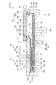
- FIG. 3 is a longitudinal sectional view of the film forming apparatus taken along the line AA in FIGS.
- FIG. 4 is a longitudinal sectional view of the film forming apparatus in which the left part of the vertical axis X is enlarged toward FIG.
- FIG. 5 is a vertical cross-sectional view of the film forming apparatus in which the right portion of the vertical axis X is enlarged toward FIG. 3.
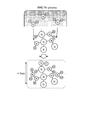
- FIG. 6 is a diagram showing an outline of the film forming process according to the first embodiment.
- FIG. 1 is a top view schematically showing a film forming apparatus according to the first embodiment.
- FIG. 2 is a plan view showing a state in which the upper portion of the processing container is removed from the film forming apparatus shown in FIG.
- FIG. 3 is
- FIG. 7 is a diagram illustrating details of the film forming process according to the first embodiment.
- FIG. 8 is a diagram showing an outline of the film forming process according to the second embodiment.
- FIG. 9 is a diagram illustrating details of the film forming process according to the second embodiment.
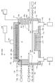
- FIG. 10 is a longitudinal sectional view of a film forming apparatus according to the third embodiment.
- FIG. 11 is a diagram illustrating details of the film forming process according to the third embodiment.
- FIG. 12 is a diagram illustrating details of the film forming process according to the fourth embodiment.
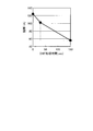
- FIG. 13 is a diagram illustrating the relationship between the DHF processing time and the film thickness.
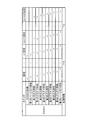
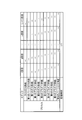
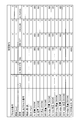
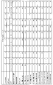
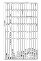
- FIG. 14A is a diagram illustrating an experimental recipe according to the first embodiment.
- FIG. 14B is a diagram illustrating an experimental recipe according to the first embodiment.
- FIG. 14C is a diagram illustrating an experimental recipe according to the first embodiment.
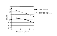
- FIG. 15A is a diagram showing a relationship between pressure and WERR in plasma post-processing.
- FIG. 15B is a diagram showing a relationship between pressure and average film thickness in plasma post-treatment.
- FIG. 15C is a diagram showing a relationship between microwave power and WERR in plasma post-processing.
- FIG. 15D is a diagram showing a relationship between microwave power and average film thickness in plasma post-treatment.
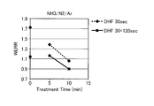
- FIG. 16A is a diagram showing the relationship between WERR and plasma post-treatment time when the reformed gas is NH 3 / N 2 / Ar.
- FIG. 16B is a diagram showing the relationship between the average film thickness, film thickness uniformity, and plasma post-treatment time when the reformed gas is NH 3 / N 2 / Ar.
- FIG. 16C is a diagram showing the relationship between WERR and plasma post-treatment time when the reformed gas is NH 3 / Ar.
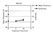
- FIG. 16D is a diagram showing the relationship between the average film thickness, film thickness uniformity, and plasma post-treatment time when the reformed gas is NH 3 / Ar.
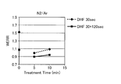
- FIG. 16E is a diagram showing the relationship between WERR and plasma post-treatment time when the reformed gas is N2 / Ar.
- FIG. 18B is a diagram illustrating TOA.
- FIG. 19A is a diagram showing the relationship between the peak area of the Si 2p 3/2 spectrum of Si—NH and the TOA according to Example 1.
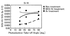
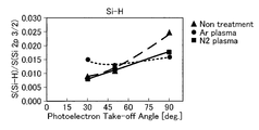
- FIG. 19B is a diagram showing the relationship between the peak area of the Si—H Si 2p 3/2 spectrum and TOA according to Example 1.
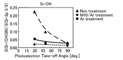
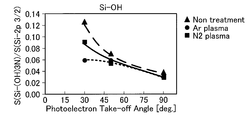
- FIG. 19C is a diagram showing the relationship between the peak area of the Si 2p 3/2 spectrum of Si—OH and the TOA according to Example 1.
- FIG. 20 is a diagram showing changes in WERR due to plasma post-treatment.
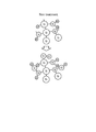
- FIG. 21A is a diagram showing an outline of oxidation of a nitride film in the case of no plasma post-treatment.
- FIG. 21A is a diagram showing an outline of oxidation of a nitride film in the case of no plasma post-treatment.
- FIG. 21B is a diagram showing an outline of termination of dangling bonds in the nitride film in the case of NH 3 / Ar plasma post-treatment.
- FIG. 21C is a diagram showing an outline of termination of dangling bonds in the nitride film when Ar plasma post-treatment is performed.
- FIG. 22A is a diagram showing changes in WERR1 and WERR2 of the comparative sample and the experimental sample when the plasma supply time during the plasma ALD sequence is 10 sec.
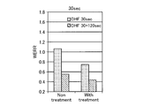
- FIG. 22B is a diagram showing changes in WERR1 and WERR2 of the comparative sample and the experimental sample when the plasma supply time during the plasma ALD sequence is 30 seconds.
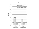
- FIG. 22C is a diagram showing changes in WERR1 and WERR2 of the comparative sample and the experimental sample when the plasma supply time during the plasma ALD sequence is 60 seconds.
- FIG. 23 is a diagram illustrating a plasma supply time and changes in WERR1 and WERR2 during the plasma ALD sequence.
- FIG. 24A is a diagram illustrating an experimental recipe according to the second embodiment.
- FIG. 24B is a diagram illustrating an experimental recipe according to the second embodiment.
- FIG. 25A is a diagram showing a comparison of WERR between Ar plasma and N 2 plasma in DCS adsorption pretreatment.
- FIG. 25B is a diagram showing an average film thickness comparison between Ar plasma and N 2 plasma in DCS adsorption pretreatment.
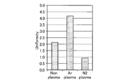
- FIG. 25C is a diagram showing a comparison of film thickness uniformity between Ar plasma and N 2 plasma in DCS adsorption pretreatment.
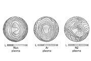
- FIG. 25D is a diagram showing a comparison in film thickness distribution between Ar plasma and N 2 plasma in DCS adsorption pretreatment.
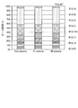
- FIG. 26 is a diagram illustrating the relationship between the waveform separation of the Si 2p 3/2 spectrum and the TOA according to the second embodiment.
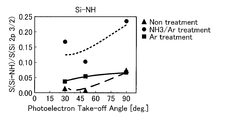
- FIG. 27A is a graph showing the relationship between the peak area of the Si 2p 3/2 spectrum of Si—NH and the TOA according to Example 2.
- FIG. 27B is a graph showing the relationship between the peak area of the Si—H Si 2p 3/2 spectrum according to Example 2 and the TOA.
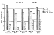
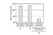
- FIG. 29B shows a sample in which a plasma ALD process without DCS adsorption pretreatment is performed for 10 seconds, a sample in which a plasma ALD process without DCS adsorption pretreatment is performed for 15 seconds, and after a DCS adsorption pretreatment is performed for 5 seconds. It is a figure which compares a film thickness average about the sample which performed ALD process only for 10 seconds.
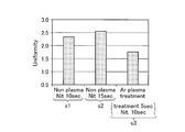
- FIG. 29C shows a sample in which the plasma ALD process without DCS adsorption pretreatment is performed for 10 seconds, a sample in which the plasma ALD process without DCS adsorption pretreatment is performed for 15 seconds, and after the DCS adsorption pretreatment is performed for 5 seconds.
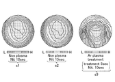
- FIG. 29D shows a sample in which a plasma ALD process without DCS adsorption pretreatment is performed for 10 seconds, a sample in which a plasma ALD process without DCS adsorption pretreatment is performed for 15 seconds, and after a DCS adsorption pretreatment is performed for 5 seconds.
- FIG. 30 is a diagram illustrating comparison of experimental results according to the second embodiment.
- FIG. 31 is a diagram illustrating an experimental recipe according to the third embodiment.
- FIG. 32 is a diagram showing the relationship between film uniformity and film thickness in Experiments 3 to 5.
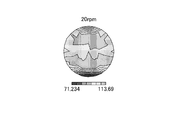
- FIG. 33 is a diagram showing the film thickness distribution in Experiment 3 along contour lines.
- FIG. 34 is a diagram showing the film thickness distribution in Experiment 4 along contour lines.
- FIG. 35 is a diagram showing the film thickness distribution in Experiment 5 in contour lines.
- a film forming apparatus 10 shown in FIGS. 1 to 5 includes, as main components, a processing container 12, a mounting table 14, a first gas supply unit 16, an exhaust unit 18, a second gas supply unit 20, and a plasma generation unit. 22.
- the film forming apparatus 10 includes a processing container 12.
- the processing container 12 is a substantially cylindrical container having a vertical axis X as a central axis.
- the processing container 12 includes a processing chamber C therein.
- the processing chamber C includes a unit U that includes an injection unit 16a.
- the processing container 12 is made of, for example, a metal such as Al (aluminum) whose inner surface is subjected to plasma-resistant processing such as anodizing or Y2O3 (yttrium oxide) thermal spraying.
- the film forming apparatus 10 includes a plasma generation unit 22 above the processing container 12.
- the plasma generation unit 22 is provided in each of four consecutive regions among the regions obtained by dividing the substantially circular surface above the processing vessel 12 into five substantially equal fan shapes around the vertical axis X.
- Each of the plasma generation units 22 includes an antenna 22a that outputs a microwave.
- the antenna 22a includes a dielectric plate 40 therein.
- the antenna 22 a includes a waveguide 42 provided on the dielectric plate 40.
- the plasma generator 22 located adjacent to the unit U in the clockwise direction is defined as a first plasma generator.
- the plasma generation unit 22 located adjacent to the first plasma generation unit in the clockwise direction is referred to as a second plasma generation unit.
- the plasma generator 22 located adjacent to the second plasma generator in the clockwise direction is referred to as a third plasma generator.
- the plasma generation unit 22 positioned adjacent to the third plasma generation unit in the clockwise direction is referred to as a fourth plasma generation unit.
- FIGS. The number of divisions of the substantially circular surface above the processing vessel 12, the number of the plasma generation units 22 provided, and the positions of the unit U and the first to fourth plasma generation units are shown in FIGS. It is not limited to what is to be done, and may be changed appropriately.
- the film forming apparatus 10 includes a mounting table 14 having a plurality of substrate mounting regions 14a on the upper surface.
- the mounting table 14 is a substantially disk-shaped plate material having the vertical axis X as a central axis.
- a recess for mounting the substrate W is formed on the upper surface of the mounting table 14.
- a plurality of concave portions are formed concentrically on a plane, and here there are five.
- the substrate W is disposed in the recess and is supported so as not to be displaced when rotated.
- the substrate placement area 14a is arranged on a circumference around the vertical axis X.
- the substrate placement area 14 a is a substantially circular concave portion that is substantially the same shape as the substantially circular substrate W.
- the diameter W1 of the recess in the substrate placement area 14a is substantially the same as the diameter of the substrate W placed in the substrate placement area 14a. That is, the diameter W1 of the concave portion of the substrate placement area 14a is set so that the substrate W does not move from the fitting position due to centrifugal force even when the placed substrate W is fitted in the concave portion and the placement table 14 rotates. What is necessary is just to fix the substrate W.
- the film forming apparatus 10 includes a gate valve G on the outer edge of the processing container 12 for carrying the substrate W into the processing chamber C and carrying the substrate W out of the processing chamber C via a transfer device such as a robot arm. Further, the film forming apparatus 10 includes an exhaust port 22 h below the outer edge of the mounting table 14. The film forming apparatus 10 maintains the pressure in the processing chamber C at a target pressure by exhausting from the exhaust port 22h.
- the processing container 12 has a lower member 12a and an upper member 12b.
- the lower member 12a has a substantially cylindrical shape opened upward, and forms a recess including a side wall and a bottom wall forming the processing chamber C.
- the upper member 12b is a lid that has a substantially cylindrical shape and forms the processing chamber C by closing the upper opening of the concave portion of the lower member 12a.
- An elastic sealing member for sealing the processing chamber C for example, an O-ring may be provided on the outer peripheral portion between the lower member 12a and the upper member 12b.
- the film forming apparatus 10 includes a mounting table 14 inside the processing chamber C formed by the processing container 12.
- the mounting table 14 is driven to rotate about the vertical axis X by the drive mechanism 24.
- the drive mechanism 24 includes a drive device 24 a such as a motor and a rotary shaft 24 b and is attached to the lower member 12 a of the processing container 12.
- the processing chamber C forms a first region R1 (not numbered in FIG. 3) and a second region R2 arranged in a plane on a circumference centered on the vertical axis X.
- the substrate W placed on the substrate placement region 14a passes through the first region R1 and the second region R2 as the placement table 14 rotates.
- the first gas supply unit 16 is disposed above the first region R ⁇ b> 1 so as to face the upper surface of the mounting table 14.
- the first gas supply unit 16 includes an injection unit 16a. That is, the area
- the injection unit 16a includes a plurality of injection ports 16h.
- the first gas supply unit 16 supplies the precursor gas to the first region R1 through the plurality of injection ports 16h.
- the precursor gas is, for example, DCS (Dichlorosilane), monochlorosilane, or trichlorosilane.
- DCS Dichlorosilane
- Si silicon
- the film forming apparatus 10 injects purge gas from the injection port 20a and exhausts the purge gas along the surface of the mounting table 14 from the exhaust port 18a. As a result, the precursor gas supplied to the first region R1 is prevented from leaking out of the first region R1. Further, since the film forming apparatus 10 ejects the purge gas from the ejection port 20a and exhausts the purge gas along the surface of the mounting table 14 from the exhaust port 18a, the reactive gas or the reactive gas radical supplied to the second region R2 And the like are prevented from entering the first region R1. That is, the film forming apparatus 10 forms a configuration in which the first region R1 and the second region R2 are separated by the injection of the purge gas from the second gas supply unit 20 and the action of the exhaust unit 18. Yes.
- the film forming apparatus 10 includes a unit U including an injection unit 16a, an exhaust port 18a, and an injection port 20a. That is, the injection part 16a, the exhaust port 18a, and the injection port 20a are formed as parts constituting the unit U.
- the unit U is configured by sequentially stacking a first member M1, a second member M2, a third member M3, and a fourth member M4.
- the unit U is attached to the processing container 12 so as to contact the lower surface of the upper member 12b of the processing container 12.
- the unit U is formed with a gas supply path 16p that penetrates the second member M2 to the fourth member M4.
- An upper end of the gas supply path 16p is connected to a gas supply path 12p provided in the upper member 12b of the processing container 12.
- a gas supply source 16g of precursor gas is connected to the gas supply path 12p via a valve 16v and a flow rate controller 16c such as a mass flow controller.
- the lower end of the gas supply path 16p is connected to a space 16d formed between the first member M1 and the second member M2.
- the injection port 16h of the injection part 16a provided in the first member M1 is connected to the space 16d.
- a gas supply path 20r penetrating the second member M2 to the fourth member M4 is formed.
- the upper end of the gas supply path 20r is connected to the gas supply path 12r provided in the upper member 12b of the processing container 12.
- a gas supply source 20g of a reaction gas is connected to the gas supply path 12r via a valve 20v and a flow rate controller 20c such as a mass flow controller.
- the lower end of the gas supply path 20r is connected to a space 20d provided between the lower surface of the fourth member M4 and the upper surface of the third member M3. Further, the fourth member M4 forms a recess for accommodating the first to third members M1 to M3. A gap 20p is provided between the side surface of the fourth member M4 forming the recess and the side surface of the third member M3. The gap 20p is connected to the space 20d.
- an exhaust passage 18q that penetrates the third member M3 to the fourth member M4 is formed.
- the upper end of the exhaust path 18q is connected to the exhaust path 12q provided in the upper member 12b of the processing container 12.
- the exhaust path 12q is connected to an exhaust device 34 such as a vacuum pump.
- the lower end of the exhaust path 18q is connected to a space 18d provided between the lower surface of the third member M3 and the upper surface of the second member M2.
- the third member M3 includes a recess that accommodates the first member M1 and the second member M2.
- a gap 18g is provided between the inner side surface of the third member M3 constituting the recess included in the third member M3 and the side end surfaces of the first member M1 and the second member M2.
- the space 18d is connected to the gap 18g.
- the lower end of the gap 18g functions as the exhaust port 18a.
- the film forming apparatus 10 ejects the purge gas from the ejection port 20a and exhausts the purge gas along the surface of the mounting table 14 from the exhaust port 18a, so that the precursor gas supplied to the first region R1 is the first region. Suppresses leakage out of R1.
- the film forming apparatus 10 includes a plasma generation unit 22 above the second region R ⁇ b> 2 that is the opening of the upper member 12 b so as to face the upper surface of the mounting table 14.
- the plasma generation unit 22 has a substantially fan-shaped opening. Four openings are formed in the upper member 12b, and the film forming apparatus 10 includes, for example, four plasma generation units 22.
- the plasma generator 22 supplies a reactive gas and a microwave to the second region R2, and generates a plasma of the reactive gas in the second region R2.
- a nitrogen-containing gas is used as the reaction gas
- the atomic layer or molecular layer chemically adsorbed on the substrate W is nitrided.
- a nitrogen-containing gas such as N2 (nitrogen) or NH3 (ammonia) can be used.
- the plasma generation unit 22 supplies the reformed gas and the microwave to the second region R2.
- plasma of the reformed gas is generated in the second region R2.
- the nitride film of the substrate W can be modified in the second region R2 by the modified gas plasma.
- the reformed gas for example, any gas of N2, NH3, Ar (argon), H2 (hydrogen), or a mixed gas in which these gases are appropriately mixed can be used.
- the supply of the precursor gas to the first region R1 is stopped during the process of modifying the nitride film of the substrate W by the plasma generation unit 22.
- an opening AP is formed in the upper member 12b of the processing container 12 so that the dielectric plate 40 is exposed to the second region R2.
- the planar size of the upper part of the opening AP is larger than the planar size of the lower part of the opening AP.
- the plane size refers to a cross-sectional area in a plane orthogonal to the vertical axis X.
- An L-shaped step surface 12s is provided in the portion of the upper member 12b that forms the opening AP.
- the edge portion of the dielectric plate 40 functions as the supported portion 40s and comes into airtight contact with the step surface 12s by an O-ring or the like. When the supported portion 40s comes into contact with the step surface 12s, the dielectric plate 40 is supported by the upper member 12b.
- the slot plate 42a is a metal plate member.
- the slot plate 42a forms the lower surface of the internal space 42i.
- the slot plate 42 a is in contact with the upper surface of the dielectric plate 40 and covers the upper surface of the dielectric plate 40.
- the slot plate 42a includes a plurality of slot holes 42s in a portion forming the internal space 42i.
- a metal upper member 42b is provided on the slot plate 42a so as to cover the slot plate 42a.
- the upper member 42b forms the upper surface of the internal space 42i of the waveguide 42.
- the upper member 42 b is screwed to the upper member 12 b so that the slot plate 42 a and the dielectric plate 40 are sandwiched between the upper member 42 b and the upper member 12 b of the processing container 12.
- the end member 42c is a metal member.
- the end member 42 c is provided at one end in the longitudinal direction of the waveguide 42. That is, the end member 42c is attached to the slot plate 42a and one end of the upper member 42b so as to close one end of the internal space 42i.
- a microwave generator 48 is connected to the other end of the waveguide 42.
- the reformed gas is any gas of N2, NH3, Ar, and H2, or a mixed gas obtained by appropriately mixing these gases.
- the third gas supply unit 22b is formed on the inner peripheral side of the opening of the upper member 12b.
- the third gas supply unit 22b includes a gas supply path 50a and an injection port 50b.
- the gas supply path 50a is formed inside the upper member 12b of the processing container 12 so as to extend around the opening AP, for example.
- An injection port 50b for injecting the reaction gas or the reformed gas toward the lower side of the dielectric window 40w is formed in communication with the gas supply path 50a.
- a gas supply source 50g of reaction gas or reformed gas is connected to the gas supply path 50a through a valve 50v and a flow rate controller 50c such as a mass flow controller.
- the plasma generation unit 22 supplies the reaction gas or the reformed gas to the second region R2 by the third gas supply unit 22b, and supplies the microwave to the second region R2 by the antenna 22a. Thereby, plasma of the reaction gas or the reformed gas is generated in the second region R2.
- the angular range in which the second region R2 extends in the circumferential direction of the vertical axis X is formed larger than the angular range in which the first region R1 extends in the circumferential direction.
- the atomic layer or molecular layer adsorbed on the substrate W is exposed to the plasma for a long time by the plasma of the reactive gas or the reformed gas generated in the second region R2, and is efficiently processed.
- a Si layer adsorbed on the substrate W is nitrided by N2 free radicals.
- an exhaust port 22 h is formed in the lower member 12 a of the processing container 12 below the outer edge of the mounting table 14.
- An exhaust device 52 is connected to the exhaust port 22h.
- the film forming apparatus 10 maintains the pressure in the second region R2 at a target pressure by exhausting from the exhaust port 22h by the operation of the exhaust device 52.
- the film forming apparatus 10 includes a control unit 60 for controlling each component of the film forming apparatus 10.
- the control unit 60 may be a computer including a control device such as a CPU (Central Processing Unit), a storage device such as a memory, an input / output device, and the like.
- the control unit 60 controls each component of the film forming apparatus 10 by the CPU operating according to the control program stored in the memory.
- the control unit 60 transmits a control signal for controlling the rotation speed of the mounting table 14 to the driving device 24a. Further, the control unit 60 sends a control signal for controlling the temperature of the substrate W to a power source connected to the heater 26. In addition, the control unit 60 sends a control signal for controlling the flow rate of the precursor gas to the valve 16v and the flow rate controller 16c. Further, the control unit 60 transmits a control signal for controlling the exhaust amount of the exhaust device 34 connected to the exhaust port 18 a to the exhaust device 34.
- control unit 60 transmits a control signal for controlling the flow rate of the purge gas to the valve 20v and the flow rate controller 20c. In addition, the control unit 60 transmits a control signal for controlling the power of the microwave to the microwave generator 48. Further, the control unit 60 transmits a control signal for controlling the flow rate of the reaction gas to the valve 50v and the flow rate controller 50c. In addition, the control unit 60 transmits a control signal for controlling the exhaust amount by the exhaust devices 34 and 52 to the exhaust device.
- FIG. 6 is a diagram showing an outline of the film forming process according to the first embodiment.
- the film forming apparatus 10 injects DCS of the housing gas onto the surface of Si-sub (substrate) which is the substrate W. Thereby, the film-forming apparatus 10 adsorbs Si contained in DCS onto Si-Sub.
- the film forming apparatus 10 injects an inert gas such as a purge gas N 2 onto the surface of the Si-sub.
- the film forming apparatus 10 purges (removes) Si (residual gas) that is excessively chemically adsorbed on the surface of the Si-sub.
- Si residual gas
- the pressure in the processing container is preferably 5 Torr or more. It has a high adsorption efficiency to the substrate.
- the film forming apparatus 10 repeats the plasma ALD sequence including the above-described series of processes (m1) cycle.
- m1 is a natural number and is the number of times that the plasma ALD sequence is repeated until the film thickness of SiN formed on the Si-sub surface reaches the target film thickness.
- the film forming apparatus 10 is a modified gas that is a gas of N2, NH3, Ar, or H2, or a mixed gas obtained by appropriately mixing these gases on the Si-sub surface on which SiN is formed. Plasma is supplied together with quality gas.
- the film forming apparatus 10 forms a nitride film having a film thickness of, for example, one atom or one molecule by executing one cycle of the plasma ALD sequence shown in FIG. Then, the film forming apparatus 10 repeatedly executes the plasma ALD sequence until the nitride film reaches, for example, 5 nm (nanometer). Thereafter, the film forming apparatus 10 performs the plasma post-treatment shown in FIG. By this plasma post-treatment, the film forming apparatus 10 improves the quality of the nitride film formed by the plasma ALD sequence.
- the film forming apparatus 10 executes the first to m1 film forming-modifying steps.
- m1 is a natural number and is the number of times the step is repeated until the target film thickness is formed by the film forming process by the film forming apparatus 10.
- Each step includes each process executed in the order of DCS gas supply, first purge gas supply, first to fourth reformed gas supply and plasma supply, and second purge gas supply.
- FIG. 7 shows that after each process of the first step is sequentially executed, the same steps are repeated until the first m1.
- One rotation of the mounting table 14 in the film forming apparatus 10 corresponds to one step.
- the film forming apparatus 10 rotates the mounting table 14 to pass the substrate W between the first region R1 and the second region R2. At this time, the film forming apparatus 10 injects the purge gas supplied from the second gas supply unit 20 onto the surface of the substrate W as the first purge gas supply process of the first step. Thereby, Si that is excessively chemically adsorbed on the substrate W is removed.
- the film forming apparatus 10 rotates the mounting table 14 to move the substrate W into the second region R2.
- the film forming apparatus 10 supplies the reaction gas containing N2 to the second region R2 by the third gas supply unit 22b of the first plasma generation unit. Further, the film forming apparatus 10 supplies the microwave from the microwave generator 48 of the first plasma generation unit to the second region R2 via the antenna 22a. Therefore, reactive gas plasma is generated in the second region R2.
- the film forming apparatus 10 further rotates the mounting table 14 and executes the same steps as the first gas supply process and the plasma supply process of the first step by the second to fourth plasma generation units. .
- the film forming apparatus 10 rotates the mounting table 14 to pass the substrate W between the second region R2 and the first region R1. At this time, the film forming apparatus 10 injects the purge gas supplied from the second gas supply unit 20 onto the substrate W as the second purge gas supply process of the first step. This completes the entire process of the first step. Then, the film forming apparatus 10 executes the second to mth steps similar to the first step.
- the processing of the first to m1th steps is a plasma ALD sequence.
- the film forming apparatus 10 repeats the same steps as the (m1 + 1) th step until the (m1 + m2) th step.
- m2 is a natural number and indicates the number of times that the same step as the (m1 + 1) th step is repeatedly executed until the film quality of the nitride film on the surface of the substrate W reaches the target film quality.
- the (m1 + 1) to (m1 + m2) th steps are called plasma post-treatment.
- the film forming apparatus 10 chemically adsorbs the precursor gas onto the surface of the substrate placed on the placing portion provided inside the processing container having airtightness. An adsorption step is performed. Then, the film forming apparatus 10 supplies a reactive gas to the inside of the processing container, generates a reactive gas plasma, and executes a first reaction step for reacting the surface of the substrate with the reactive gas plasma.
- the film forming apparatus 10 is a reforming gas that is a mixture of ammonia gas, argon gas, nitrogen gas, or hydrogen gas or ammonia gas, argon gas, nitrogen gas, or hydrogen gas.
- a gas is supplied, a plasma of the reformed gas is generated, and a second reaction step is performed in which the surface of the substrate reacts with the plasma of the reformed gas. Therefore, the film quality of the nitride film is improved while increasing the throughput of generating the nitride film on the substrate. In addition, a nitride film can be formed on the plate with high coverage.
- the film forming apparatus 10 since the film forming apparatus 10 repeatedly performs the adsorption step and the first reaction step and then executes the second reaction step, the film quality of the nitride film is efficiently improved.
- the film forming apparatus 10 since the film forming apparatus 10 repeatedly performs a series of processes for performing the second reaction step after the adsorption step and the first reaction step are sequentially repeated, the film thickness of the nitride film is ensured. Efficiently improve the quality of the nitride film.
- the film forming apparatus 10 continuously executes the plasma ALD sequence and the plasma post-treatment on the substrate W placed on the mounting table 14 by the rotation of the mounting table 14. Further, the film forming apparatus 10 can control the processing times T11 and T12. Therefore, the deposition apparatus 10 further improves the throughput of the deposition process.
- the film forming apparatus 10 may perform a series of plasma ALD sequences and plasma post-processing subsequent to the plasma ALD sequence a plurality of times. In other words, the film forming apparatus 10 may perform a series of plasma ALD sequences and plasma post-processing as a single process, and may execute the process multiple times.
- the film forming apparatus 10 performs the first plasma post-treatment on a nitride film of, for example, 5 nm formed on the substrate W in the first series of plasma ALD sequences.
- the film forming apparatus 10 then executes a second series of plasma ALD sequences on the substrate W that has been subjected to the first plasma post-treatment. Then, a further 5 nm nitride film is formed on the substrate W, for example.
- the film forming apparatus 10 performs the second plasma post-processing (plasma reforming process) on the 5 nm nitride film further formed on the substrate W in the first series of plasma ALD sequences.
- a nitride film modified every 5 nm can be stacked on the substrate W, and a high-quality nitride film can be efficiently formed.
- a 10 nm nitride film may be formed on the substrate W at a time, and the plasma post-treatment may be performed on the 10 nm nitride film formed on the substrate W by the plasma ALD sequence.
- the configuration of the film forming apparatus in the second embodiment is the same as that in the first embodiment.
- the second embodiment is different from the first embodiment in that a DCS adsorption pre-processing described later is executed before a DCS adsorption processing described later in the plasma ALD sequence.
- a film forming process performed by the film forming apparatus according to the second embodiment will be described.
- FIG. 8 is a diagram showing an outline of the film forming process according to the second embodiment. Note that the pre-stage process of the film forming process is the same as that of the first embodiment.
- initial nitridation for generating a nitride film by Ar or N 2 plasma on the surface of Si-sub that is the substrate W is executed.
- the film forming apparatus 10a appropriately mixed Ar, N2, or these gases into the Si-sub surface on which SiN is formed. Plasma is supplied together with the reaction gas of the reformed gas that is a mixed gas. This process is called DCS adsorption pretreatment.
- the film forming apparatus 10a adsorbs Si contained in the DCS by injecting DCS onto the Si-sub surface (SiN film).
- the film forming apparatus 10a injects an inert gas such as N2 onto the surface of the Si-sub (Si layer), thereby excessively adsorbing Si on the surface of the Si-sub (Si layer). Purge (residual gas). When the excessively chemically adsorbed Si is removed from the Si-sub surface, a chemically adsorbed Si layer remains on the Si-sub surface.
- the film forming apparatus 10a supplies a plasma together with a reaction gas such as NH3 to the surface of the Si-sub (Si layer) from which Si that has been excessively adsorbed on the surface is removed.
- the adsorbed Si layer is nitrided (nitrided).
- SiN is formed on the Si-sub surface.
- the film deposition apparatus 10a purges impurities (residues and the like) from the Si-sub surface by injecting an inert gas such as N2 onto the Si-sub surface on which SiN is deposited. .
- the process from Adsorption to Purge is called DCS adsorption process.
- the plasma treatment with the reformed gas is performed after the plasma ALD sequence.
- the plasma process using the reformed gas is included in one cycle of the plasma ALD sequence. That is, every time one cycle of the plasma ALD sequence is executed and a nitride film layer of only one atom or one molecule is formed on the Si-sub surface, the plasma treatment with the reformed gas is executed.
- FIG. 9 is a diagram illustrating details of the film forming process according to the second embodiment.
- the pre-stage process of the film forming process 10a according to the second embodiment is the same as that of the first embodiment.
- the film forming apparatus 10a sequentially executes the first to fourth gas supply processes and the plasma supply process as the first step, as in the (m1 + 1) th step of the first embodiment. To do.
- the film forming apparatus 10a sequentially executes the second purge gas supply process as the first step.
- the gas supplied in the first to fourth gas supply processes in the first step is the same reformed gas as in the first embodiment.
- the step on the first day is called a pre-DCS adsorption step.
- the film forming apparatus 10a executes the same step as the first step of the first embodiment as the second step.
- the second step is called a DCS adsorption step.
- the film forming apparatus 10a sequentially executes the pre-DCS adsorption step and the DCS adsorption step, which are the same as the first to second steps, until the nth to (n + 1) th steps.
- n is a natural number, and is the number of times the DCS adsorption pre-step and the DCS adsorption step are repeated until a nitride film having a target film quality is formed by the film forming process by the film forming apparatus 10a.
- the time T21 for the film forming apparatus 10a to execute the first to (n + 1) th steps can be appropriately changed by controlling the rotation speed of the mounting table 14 by the control unit 60.
- the film forming apparatus 10 a according to the second embodiment continuously executes a plasma ALD sequence with DCS adsorption pretreatment on the substrate W placed on the placement table 14 by the rotation of the placement table 14. Further, the film forming apparatus 10a can control the processing time T21. Therefore, the film forming apparatus 10a further improves the throughput of the film forming process.
- the film-forming apparatus 10a adsorb
- a second reaction step is performed to react.
- the film forming apparatus 10a repeatedly performs a series of processes of the adsorption step, the first reaction step, and the second reaction step by sequentially rotating the mounting table 14, for example, for each film thickness of one atom or one molecule.
- the film quality of the nitride film can be improved, and a better quality nitride film can be efficiently formed.
- FIG. 10 is a longitudinal sectional view of a film forming apparatus according to the third embodiment.
- the film forming apparatus 100 according to the third embodiment has the same function as the film forming apparatus 10 according to the first and second embodiments.
- the film forming apparatus 10 according to the first and second embodiments allows the substrate to pass through each processing area in which the processing chamber is radially divided for each process by the rotation of the mounting table 14. Thereby, a series of processes and steps are continuously performed on the substrate.
- the film forming apparatus 100 according to the third embodiment supplies a gas used for processing for each process and step to a substrate on a mounting table in a processing chamber that is not partitioned, and the gas after the processing Exhaust.
- the film forming apparatus 100 includes, for example, a bottomed cylindrical processing container 112 having an open top surface.
- the processing container 112 is made of, for example, an aluminum alloy. Further, the processing container 112 is grounded.
- a mounting table 114 for mounting the substrate W, for example, is provided at a substantially central portion of the bottom of the processing container 112.
- the mounting table 114 includes a heater 126.
- the heater 126 is connected to a DC power source (not shown) provided outside the processing container 112.
- the heater 126 generates heat by the direct current power source, and heats the substrate W placed on the placement table 114.
- a dielectric window 140w is provided via an elastic sealing member such as an O-ring that seals the region R in the processing container 112.
- the processing container 112 is closed by the dielectric window 140w.
- a plasma generator 122 that supplies microwaves for plasma generation is provided above the dielectric window 140w.
- the waveguide 142 which leads to the microwave generator 148 is connected to the cover member on the upper surface of the plasma generation unit 122.
- the microwave generator 148 generates a microwave.
- a gas supply port 116a for supplying gas is formed in the upper part of the inner peripheral surface of the processing vessel 112 covering the outer peripheral surface of the region R.
- the gas supply ports 116a are formed evenly at a plurality of locations along the inner peripheral surface of the processing container 112, for example.
- a gas supply path 116p that penetrates the side wall of the processing container 112 and is connected to a gas supply source 116g installed outside the processing container 112 is connected to the gas supply port 116a.
- a gas supply source 116g is connected to the gas supply path 116p through a valve 116v and a flow rate controller 116c such as a mass flow controller.
- the gas supply unit 116 includes a gas supply port 116a, a flow rate controller 116c, a gas supply path 116p, and a valve 116v, so that a gas can be supplied to the region R in the processing container 112 from above.
- a gas supply port 120a for supplying gas is formed in the middle portion of the inner peripheral surface of the processing vessel 112 that covers the outer peripheral surface of the region R.
- the gas supply ports 120a are formed at a plurality of locations along the inner peripheral surface of the processing vessel 112, for example.
- a gas supply path 120p that penetrates the side wall of the processing vessel 112 and is connected to a gas supply source 120g installed outside the processing vessel 112 is connected to the gas supply port 120a.
- a gas supply source 120g is connected to the gas supply path 120p through a valve 120v and a flow rate controller 120c such as a mass flow controller.
- the gas supply unit 120 includes a gas supply port 120a, a flow rate controller 120c, a gas supply path 120p, and a valve 120v, so that gas can be supplied from the side to the region R in the processing container 112.
- a substantially annular gas supply ring 130r disposed in a positional relationship surrounding the outer periphery of the substrate W mounted on the mounting table 114 is formed above the mounting table 114.
- the gas supply ring 130r is, for example, a substantially annular gas pipe.
- the gas supply ring 130r is formed with a plurality of gas supply holes for supplying gas from above the outer periphery of the substrate W to the substrate W on the mounting table 114 on the surface of the tube.
- a gas supply path 130p that penetrates the side wall of the processing container 112 and communicates with a gas supply source 130g installed outside the processing container 112 is connected to the gas supply ring 130r.
- the gas supply ring 130r is supported substantially parallel to the mounting table 114 and the substrate W on the mounting table 114 by the support column 130s.
- a gas supply source 130g is connected to the gas supply path 130p through a valve 130v and a flow rate controller 130c such as a mass flow controller.
- the gas supply unit 130 includes a gas supply ring 130r, a flow rate controller 130c, a gas supply path 130p, and a valve 130v, so that the substrate W on the mounting table 114 in the processing container 112 is close to the substrate W on the outer periphery. Gas can be fed from.
- the gas supply ring 130r is also called an ALD ring.
- region R is provided in the both sides which sandwich the mounting base 114 of the bottom part of the processing container 112. As shown in FIG.
- the exhaust unit 118 exhausts the gas in the region R through the exhaust port 118a by the operation of the exhaust device 134 such as a vacuum pump. By exhausting from the exhaust port 118a, the pressure in the region R is maintained at a target pressure.
- the region R is closed after the substrate W is mounted on the mounting table 114 of the film forming apparatus 100. Then, the film forming apparatus 100 supplies the reaction gas containing N 2 to the region R by the gas supply source 116g. Then, the film forming apparatus 100 supplies the microwave output from the microwave generator 148 to the region R via the plasma generation unit 122. Thereby, in the region R, plasma of the reactive gas is generated. The surface of the substrate W is nitrided by the reactive gas plasma.
- the pre-stage process is called initial nitriding.
- the film forming apparatus 100 sequentially executes the first to p1th steps.
- p1 is a natural number and is the number of times the step is repeated until the target film thickness is formed by the film forming process by the film forming apparatus 100.
- Each step includes each process executed in the order of DCS gas supply, first exhaust, first purge gas supply, gas supply, plasma supply, second exhaust, and second purge gas supply.
- FIG. 11 shows that after each process of step 1 is executed sequentially, the same steps are repeated until the p1th step.
- the film forming apparatus 100 exhausts the gas in the region R by the exhaust apparatus 134 to make a vacuum state.
- the film forming apparatus 100 injects the purge gas supplied from the gas supply unit 116 onto the substrate W as the first purge gas supply process of the first step. Thereby, Si that is excessively chemically adsorbed on the substrate W is removed.
- the film forming apparatus 100 exhausts the gas in the region R by the exhaust apparatus 134 to make a vacuum state.
- the film forming apparatus 100 injects the purge gas supplied from the gas supply unit 116 onto the substrate W as the second purge gas supply process of the first step.
- Si that is excessively chemically adsorbed on the substrate W is removed. This completes the entire process of the first step.
- the film forming apparatus 100 sequentially executes the second to p1th steps similar to the first step. Steps 1 to p1 are called a plasma ALD sequence.
- the film forming apparatus 100 performs steps of DCS gas supply, first exhaust, first purge gas supply, gas supply and plasma supply, second exhaust, and second purge gas supply to the substrate W. Is repeated p1 times. Thereby, a silicon nitride film having a target film thickness is formed on the substrate W.
- the gas supplied in the gas supply process in the (p1 + 1) to (p1 + p2) th steps is any gas of N2, NH3, Ar, H2, or a mixed gas in which these gases are appropriately mixed. It is a reformed gas.
- the gas supplied in the second purge gas supply process of the (p1 + 1) th step is an inert gas such as Ar.
- the (p1 + 1) to (p1 + p2) th steps are called plasma post-treatment. Note that the time T31 when the film forming apparatus 100 executes the first to p1th steps and the time T32 when the (p1 + 1) to (p1 + p2) th steps are executed can be changed as appropriate under the control of the control unit 160.
- the gas discharge process in the processing container can be omitted, so that the processing efficiency is increased.
- the film forming apparatus 100 has a relatively simple configuration, efficiently improves the film quality of the nitride film, and ensures the film thickness of the nitride film. And improvement in film quality can be achieved.
- the configuration of the film forming apparatus is the same as that in the third embodiment.
- the fourth embodiment is different from the third embodiment in that a DCS adsorption pretreatment described later is executed before a DCS adsorption treatment described later in the film forming process.
- a film forming process performed by the film forming apparatus according to the fourth embodiment will be described.
- a film forming apparatus according to the fourth embodiment is a film forming apparatus 100a.
- FIG. 12 is a diagram illustrating details of the film forming process according to the fourth embodiment.
- the pre-stage process of the film forming process according to the fourth embodiment is the same as that of the third embodiment.
- the film forming apparatus 100a performs each of gas supply and plasma supply, second exhaust, and second purge gas supply as the first step, as in the (p1 + 1) time of the third embodiment. Run processes sequentially.
- the gas supplied in the gas supply process of the first step is the same reformed gas as in the third embodiment. Similar to the second embodiment, the first step is referred to as a DCS adsorption pre-step.
- the gas supplied in the gas supply process of the first step is preferably a single N 2 gas or a single Ar gas.
- the film forming apparatus 100a executes the same step as the first step of the third embodiment as the second step. Similar to the second embodiment, the second step is referred to as a DCS adsorption step. Then, the film forming apparatus 100 performs the DCS pre-adsorption step and the DCS adsorption step similar to the first and second steps until the q to (q + 1) th steps.
- q is a natural number, and is the number of times that the DCS adsorption pre-step and the DCS adsorption step are repeated until a nitride film having a target film quality is formed by the film forming process by the film forming apparatus 100.
- the time T41 for the film forming apparatus 100a to execute the first to (q + 1) -th steps can be changed as appropriate under the control of the control unit 160.
- the film forming apparatus 100a can efficiently form a high-quality nitride film with a relatively simple configuration.
- the film formation by the film formation apparatus 10a according to the second embodiment may be performed on the substrate that has been subjected to the plasma post-treatment after being formed by the film formation apparatus 10 according to the first embodiment.
- film formation by the film formation apparatus 100a according to the fourth embodiment may be performed on a substrate that has been subjected to plasma post-treatment after being formed by the film formation apparatus 100 according to the third embodiment. Thereby, the film quality of the nitride film and the throughput of the film formation can be made compatible.
- film formation by the film formation apparatus 10a according to the second embodiment is performed on the substrate that has been subjected to plasma post-treatment after being formed by the film formation apparatus 10 according to the first embodiment, and further, the film formation apparatus 10 After film formation by plasma, plasma post-treatment may be performed.
- film formation by the film formation apparatus 100a according to the fourth embodiment is performed on a substrate that has been subjected to plasma post-treatment after being formed by the film formation apparatus 100 according to the third embodiment, and the film formation apparatus 100 is further performed. After film formation by plasma, plasma post-treatment may be performed. Thereby, the film quality of the nitride film and the throughput of the film formation can be made compatible.
- the film quality is modified, and further, the film formation apparatus 10a.
- the film may be formed.
- the film quality of the substrate formed by the film formation apparatus 100a according to the fourth embodiment is modified after the film formation by the film formation apparatus 100 according to the third embodiment, and the film formation apparatus 100a is further modified.
- the film may be formed. Thereby, the film quality of the nitride film and the throughput of the film formation can be made compatible.
- the nitride film is formed on the surface of the substrate using the ALD method.
- the present invention is not limited to this, and the surface of the substrate is nitrided using the MLD method.
- a film may be formed.
- the case where the DCS adsorption pre-step and the DCS adsorption step are repeated has been described as an example, but the present invention is not limited to this.
- the DCS adsorption step also referred to as the third reaction step
- the same process as the DCS pre-adsorption step is performed before supplying the reformed gas. May be. That is, before the second reaction step, a gas containing at least one of argon gas and nitrogen gas is supplied into the processing vessel, and plasma of the supplied gas is generated and reacted with the surface of the substrate.
- Three reaction steps may be included. As a result, the number of steps can be reduced, and a high-quality nitride film can be formed.
- the film formation control program shown in each of the above embodiments may be recorded on a recording medium that can be read and written by light or magnetism, or a storage device using a semiconductor element.
- the storage medium is a DVD, SD, flash memory, Blu-ray disc, or the like. Or you may make a computer acquire a control program from the other computer which read the control program from the memory
- Example 1 according to Embodiment 3 described above will be described below.
- Example 1 performed using the film forming apparatus 100 according to the above-described third embodiment will be described.
- Experiment 1 performed using the film forming apparatus 100 according to the above-described third embodiment will be described.
- an experimental sample in which plasma post-processing was performed was evaluated. This verified the improvement of the quality of the nitride film.
- the film quality of the nitride film is evaluated not only by oxidation resistance but also by film thickness, film thickness uniformity, film formation distribution, and the like.
- the execution conditions of the plasma ALD sequence in which a nitride film was formed on the surface of the silicon wafer were as follows.
- As the reaction gas a mixed gas of NH3 / N2 / Ar was used.
- the pressure during film formation was 5 Torr.
- the microwave power supplied during film formation was 4 kW.
- the processing time was 10 sec (seconds).
- WERR when the experimental sample was immersed in DHF for 30 seconds was set to WERR1
- a sample that was not subjected to plasma post-treatment was used as a comparative sample.
- the improvement effect of the nitride film by plasma post-processing was evaluated by calculating and comparing WERR1 and WERR2 about both an experimental sample and a comparative sample. Note that WERR indicates that the smaller the value, the better the etching resistance and the better the film quality.
- WERR1 is an index for evaluating the surface quality of the sample nitride film and the vicinity of the surface.
- WERR2 is an index for evaluating the quality of the sample nitride film.
- DHF immersion is referred to as DHF treatment.
- FIG. 13 is a diagram showing the relationship between the DHF processing time and the film thickness.
- FIG. 13 shows the relationship between the DHF processing time and the film thickness, with the DHF processing time (sec) on the horizontal axis and the film thickness (A (angstrom)) on the vertical axis.
- the film thickness decreased as the DHF treatment time increased. More specifically, the slope of the straight line between the DHF processing time of 0 sec and about 30 sec is larger than the slope of the straight line between about 30 sec and 150 sec.
- the surface of the nitride film and the vicinity of the surface are more easily etched than in the film, and the film quality near the surface of the nitride film and the surface thereof is inferior to that in the film.
- WERR WERR1
- WERR2 WERR2
- Example 1 (Experimental recipe) In Example 1, Experiment 1 was performed according to the experimental recipe shown in FIGS. 14A to 14C. As shown in FIG. 14A, processes having process numbers 1 to 6 were executed as initial nitriding. Further, as shown in FIG. 14B, processes with process numbers 7 to 17 were executed as the plasma ALD sequence. In the plasma ALD sequence, the processes of Nos. 7 to 16 were repeated 200 times. Further, as shown in FIG. 14C, processes with process numbers 18 to 23 were executed as plasma post-treatment. In the plasma post-treatment, a series of processes Nos. 18 to 22 were repeated 5 times.
- MW OFF is a microwave stop process.
- VACUUM is a gas discharge process.
- Ar PURGE is a purge gas supply process.
- ADSORPTION is a DCS adsorption process.
- TREAT is a reformed gas and plasma supply process in plasma post-processing.
- KEEP is a gas supply maintenance process performed after the microwave is stopped in the plasma post-process.
- the “pressure” corresponding to each process number is the pressure in the region R of the film forming apparatus 100.
- the “Ar flow rate” is a flow rate of Ar supplied from above to the region R through the gas supply port 116a.
- the “N2 flow rate” is a flow rate of N2 supplied from above to the region R through the gas supply port 116a.
- the “O2 flow rate” is a flow rate of O2 (oxygen) supplied from above to the region R through the gas supply port 116a.
- the “NF3 flow rate” is the flow rate of NF3 (nitrogen trifluoride) supplied from above to the region R through the gas supply port 116a.
- the “Ar-edge flow rate” is the flow rate of Ar supplied from the side to the region R through the gas supply port 120a.
- the “Ar-ring flow rate” is the flow rate of Ar injected to the substrate W through the ALD ring.
- the “DCS-ring flow rate” is a flow rate of DCS injected to the substrate W through the ALD ring.
- the “NH3-edge flow rate” is a flow rate of NH3 supplied from the side to the region R through the gas supply port 120a.
- the “SiH4-edge flow rate” is a flow rate of SiH 4 (monosilane) supplied from the side to the region R through the gas supply port 120a.
- the “N2-edge flow rate” is a flow rate of N2 supplied from the side to the region R through the gas supply port 120a.
- the “microwave output” is the microwave power supplied to the plasma generation unit 122.
- FIG. 14A shows that the plasma supply process was executed for 5 seconds in the third process.
- the pressure in the region R is set to 5 torr, and 900 SCCM Ar and 900 SCCM N2 are supplied to the region R from above through the gas supply port 116a.
- 200 SCCM Ar and 400 SCCM NH 3 are supplied from the side to the region R through the gas supply port 120a.
- it shows that 100 SCCM of Ar is injected onto the substrate W through the ALD ring.
- it shows that a 4000 W microwave was supplied to the plasma generation unit 122.
- FIG. 14A shows the supply positions and component ratios of the supplied reaction gas and reformed gas. The same applies to FIGS. 14B and 14C.
- the WERR is reduced as the pressure is increased in the plasma post-treatment, so that the effect of improving the quality of the nitride film is high.
- the effect of improving WERR1 which is the WERR of the experimental sample by the 30 sec DHF treatment, is remarkable.
- WERR2 which is a WERR indicating the quality of the nitride film by 30 + 120 sec DHF treatment, deteriorated at 1 Torr, unchanged at 3 Torr, and improved at 5 Torr.
- WERR1 was improved by any reforming gas of NH3 / N2 / Ar, NH3 / Ar, N2 / Ar, and Ar. That is, the improvement of the surface of the nitride film and the vicinity of the surface was recognized by any modified gas.
- FIGS. 17A and 17B are diagrams showing the depth of modification of the nitride film by the plasma post-treatment.
- an experimental sample in which plasma post-treatment was performed for 5 min with a mixed gas of NH 3 / N 2 / Ar was defined as the first experimental sample.
- An experimental sample in which plasma post-treatment was performed for 10 min with a mixed gas of NH 3 / N 2 / Ar was used as a second experimental sample.
- An experimental sample in which a plasma post-treatment was performed for 5 min with a mixed gas of NH 3 / Ar was used as a third experimental sample.
- an experimental sample in which a plasma post-treatment was performed for 10 min with a mixed gas of NH 3 / Ar was used as a fourth experimental sample.
- the sample which did not perform plasma post-processing was made into the comparison sample.
- DHF treatment was performed on five samples, that is, the first to fourth experimental samples and the comparative sample that was not subjected to the plasma post-treatment.
- FIG. 17A is a diagram showing a measurement result of Mean Thickness. Any of the 5 and 10 min DHF treatments was performed on the third and fourth experimental samples in which the plasma post-treatment with the mixed gas of NH 3 / Ar having the highest effect of modifying the nitride film was performed. As a result, as shown in FIG. 17A, the mean thickness of each experimental sample was reduced by about 50A.
- the decrease rate of Mean Thickness according to the processing time when the comparative sample and the first and third experimental samples are DHF-treated is such that the third experimental sample has a DHF treatment time of about 50 seconds or later. It became the minimum.
- the decrease rate of Mean Thickness according to the processing time of the DHF processing corresponds to the slope of the straight line in FIG. 17B.
- the slope of the straight line is the wet etching rate (A / sec). If the slope of the straight line is small, it indicates that the wet etching rate is slow and the film quality is good.
- the film quality was improved in the third experimental sample in which the plasma post-treatment with the NH 3 / Ar modified gas was performed.
- the wet etching rate in the vicinity of the first experimental sample 150 sec is also smaller than the comparative sample in which the plasma post-treatment was not performed.
- the remaining film at that time was 5 nm.
- the film thickness of as depo of the first experimental sample was 10 nm.
- the peak separation of spin 1/2, 3/2 is 0.06 eV
- the peak intensity ratio is 1: 2
- peak separation is performed, and the signal of spin 1/2 is obtained from the Si 2p spectrum. Removed. The peak position was aligned with the signal peak 99.2 eV of the silicon substrate.
- ⁇ shown in FIG. 18B is an escape angle (TOA: Take Off Angle) of photoelectrons that escape from the nitride film when the nitride film is irradiated with X-rays using angle-resolved XPS (photoelectron spectroscopy).
- TOA Take Off Angle
- ⁇ (nm) shown in FIG. 18B is the attenuation length of the photoelectrons. That is, ⁇ ⁇ sin ⁇ ( ⁇ ⁇ the sine value of theta) is the escape depth of photoelectrons that can escape due to the photoelectric effect by X-ray irradiation.
- the symbol “Si3 +” in the waveform separation result graph shown in FIG. 18A represents a bonding state in which three Ns and one Si are bonded around the focused Si atom.
- 19A, 19B, and 19C show the results of normalizing each separation peak area with the peak area of the Si2p 3/2 spectrum in order to evaluate the ratio of the bonded state in the film.
- the peak area means the area of the peak signal of the Si 2p 3/2 spectrum of the substance.
- the peak area ratio indicates the ratio of the peak area of each chemical bond state to the total area of the peak signal of the Si 2p 3/2 spectrum of the compound.
- the Si—NH bond of the NH 3 / Ar plasma has a larger peak area ratio than the other conditions, without depending on TOA. This indicates that the Si—NH bond in the film has increased.
- FIG. 20 is a diagram showing changes in WERR due to plasma post-treatment.
- the improvement in the surface film quality of the nitride film was confirmed by the plasma post-treatment.
- the improvement in the surface film quality of the nitride film is thought to be due to an increase in NH bonds in the film. That is, it is considered that the dangling bonds in the film are terminated by the supply of NH radicals by the plasma post-treatment, and the oxidation reaction between the oxidizing components in the atmosphere and dangling bonds during exposure to the atmosphere is suppressed.
- the NH 3 / Ar plasma post-treatment improves the film quality not only on the surface of the nitride film but also in the film.
- FIG. 21A is a diagram showing an outline in which the nitride film is oxidized by bonding the dangling bonds of the nitride film with an oxidizing component in the atmosphere without plasma post-treatment.
- FIG. 21B is a diagram showing an outline of termination of dangling bonds of N atoms in the nitride film when NH 3 / Ar plasma post-treatment is performed. As shown in FIG. 21B, N-bond dangling bonds (DB (Dangling Bond)) are terminated by NH3 radicals, so that N-bonding dangling bonds of the nitride film are reduced and oxidation components in the atmosphere are reduced. It is thought that the binding of was suppressed.
- DB Direct Bond
- the DB termination by NH radicals extends to the depth of about 5 nm from the film surface of the nitride film. it is conceivable that.
- FIG. 21C is a diagram showing an outline of termination of dangling bonds of N atoms when Ar plasma post-treatment is performed. As shown in FIG. 21C, it is considered that the bond between the H atom and the Si atom was broken as a result of the collision between the H atom bonded to the Si atom in the nitride film and the Ar ion. Then, it is considered that the bond between the N atom dangling bond and the Si atom is bonded to reduce the dangling bond of the N atom in the nitride film, and the bond with the oxidizing component in the atmosphere is suppressed. Note that the modification effect of the nitride film by the Ar plasma post-treatment was observed only on the film surface, so it is considered that DB bonding due to ion collision occurred on the film surface of the nitride film.
- FIGS. 22A to 22C and FIG. 23 are diagrams showing the relationship between the plasma ALD sequence, that is, the plasma supply time at the time of forming the nitride film, and the effect of the plasma post-treatment.
- the execution conditions of the plasma post-processing executed for the experimental samples in FIGS. 22A to 22C and FIG. 23 were a pressure of 5 Torr, a microwave power of 4 kW, and an execution time of 5 min.
- a sample without plasma post-treatment was used as a comparative sample
- a sample with plasma post-treatment was used as an experimental sample.
- FIG. 22A is a diagram showing changes in WERR1 and WERR2 of the comparative sample and the experimental sample, respectively, when the plasma supply time during the plasma ALD sequence is 10 sec.
- FIG. 22B is a diagram showing changes in WERR1 and WERR2 of the comparative sample and the experimental sample, respectively, when the plasma supply time at the time of forming the nitride film is 30 seconds.
- FIG. 22C is a diagram showing changes in WERR1 and WERR2 of the comparative sample and the experimental sample, respectively, when the plasma supply time when forming the nitride film is 60 seconds.
- FIG. 23 is a diagram showing changes in plasma supply time and WERR1 and WERR2 during the plasma ALD sequence.
- the longer the plasma supply time during the plasma ALD sequence the smaller the amount of change in WERR1 and WERR2 due to the plasma post-treatment.
- the shorter the plasma supply time during the film formation by the plasma ALD sequence the higher the change amount of WERR1 and WERR2 due to the plasma post-treatment. Since the amount of change in WERR1 is large compared to WERR2 regardless of the plasma supply time, it can be said that the effect of improving the film quality by plasma post-treatment is greater at the surface and in the vicinity of the surface than in the nitride film.
- a nitride film having a good film quality is formed by repeating the process of shortening the plasma ALD sequence processing time, forming a relatively thin nitride film, and improving the film quality by plasma post-treatment. I can say that. Therefore, even if the execution time of the entire film formation process is shortened, a good nitride film can be formed, and the throughput of the entire film formation process can be improved.
- Example 2 according to the above embodiment will be described below.
- Experiment 2 performed using the film forming apparatus 100a according to the above-described fourth embodiment will be described.
- the plasma of the reformed gas was supplied before forming the nitride film on the silicon wafer substrate by the plasma ALD method.
- denaturation of the nitride film was verified by evaluating the experimental sample which performed the film-forming process after that. Unless otherwise specified, the execution conditions for each process are the same as those in the first embodiment.
- the execution conditions of the plasma ALD sequence in which a nitride film was formed on the surface of the silicon wafer were as follows.
- As the reforming gas a mixed gas of NH3 / N2 / Ar was used.
- the pressure during the DCS adsorption treatment was 5 Torr.
- the electric power of the microwave supplied at the time of DCS adsorption processing was 4 kW.
- the processing time of the plasma ALD sequence was 10 sec (seconds).
- the execution conditions of the DCS adsorption pretreatment included in the plasma ALD sequence were as follows. That is, as the reformed gas, two patterns of single N2 gas and single Ar gas were used. The pressure for the DCS adsorption pretreatment was 5 Torr. In addition, the microwave power supplied during the DCS adsorption pretreatment was 4 kW. The processing time was 2 patterns of 5 sec. The flow rate of the reformed gas from the ALD ring was set to three patterns of 100, 300, and 500 SCCM. The total flow rate of the reformed gas was 500, 1000, and 1500 SCCM, respectively, with respect to the flow rate of the reformed gas from the ALD ring.
- FIG. 25A to FIG. 25D are diagrams showing a comparison between Ar plasma and N 2 plasma in DCS adsorption pretreatment.
- WERR1 and WERR2 were improved in both the Ar plasma DCS adsorption pretreatment and the N2 plasma DCS adsorption pretreatment as compared with the DCS adsorption pretreatment.
- improvement in WERR1 and WERR2 was greater with Ar plasma DCS adsorption pretreatment than with N2 plasma DCS adsorption pretreatment.
- the average film thickness decreased in both the Ar plasma DCS adsorption pretreatment and the N2 plasma DCS adsorption pretreatment as compared with the DCS adsorption pretreatment.
- the decrease in the average film thickness was greater with Ar plasma DCS adsorption pretreatment than with N2 plasma DCS adsorption pretreatment.
- FIGS. 25C and 25D compared with the DCS adsorption pretreatment, the film thickness uniformity deteriorated with the Ar plasma DCS adsorption pretreatment, but with the N2 plasma DCS adsorption pretreatment, the film thickness uniformity. Improved.
- FIG. 25D is a figure which shows film thickness distribution by a contour line. The hatching legend in FIG. 25D indicates that the film thickness is lower toward the left and the film thickness is higher toward the left as viewed in FIG. 25D.
- the Ar plasma DCS adsorption pretreatment was superior to the N2 plasma DCS adsorption pretreatment.
- the N2 plasma DCS adsorption pretreatment was superior to the Ar plasma DCS adsorption pretreatment.
- FIG. 26 is a diagram illustrating a waveform separation result of the Si 2p 3/2 spectrum, similar to FIG. 18 illustrated in the first embodiment.
- the three vertical graphs in the left column of FIG. 26 correspond to comparative samples without DCS adsorption pretreatment. Further, the three vertical graphs in the middle row of FIG. 26 correspond to the experimental sample in which the Ar plasma DCS adsorption pretreatment was executed. Further, the three vertical graphs in the right column of FIG. 26 correspond to the experimental sample in which the N2 plasma DCS adsorption pretreatment was executed.
- the separation peak area of Si—NH is the largest. That is, the signal intensity of the Si—NH bond of the experimental sample subjected to the Ar plasma DCS adsorption pretreatment is stronger than that of the other samples.
- 27A, 27B, and 27C show the results of normalizing each separation peak area with the peak area of the Si 2p 3/2 spectrum in order to evaluate the ratio of the bonded state in the film.
- the Si—NH bond in the Ar plasma DCS adsorption pretreatment had a large peak area ratio independent of TOA compared to other conditions. This indicates that the Si—NH bond in the film has increased. Further, as shown in FIG. 27B, since the peak area of Si—H occupying the entire peak area was small, it can be said that the change amount of the entire peak area accompanying the change amount of the peak area of Si—H is small.
- FIG. 28 is a diagram showing a comparison of the ratio of the peak area of the Si 2p 3/2 spectrum for each composition component of the nitride film in which Ar plasma and N 2 plasma were executed in the DCS adsorption pretreatment.
- TOA when TOA is 90 °, there is no DCS adsorption pretreatment, Ar plasma DCS adsorption pretreatment, and N2 plasma DCS adsorption pretreatment, and there is almost no difference in the peak area ratio of each bond. It was.
- FIGS. 27A and 27C when the TOA was reduced to 30 °, the Si—NH bond strength increased and the Si—OH bond strength decreased. Therefore, it can be said that the effect of suppressing the surface oxidation was great by the DCS adsorption pretreatment.
- FIGS. 29A to 29D show a sample in which the plasma ALD process without DCS adsorption pretreatment is executed for 10 seconds, a sample in which the plasma ALD process without DCS adsorption pretreatment is executed for 15 seconds, and the DCS adsorption pretreatment is executed for 5 seconds.
- FIG. 4 is a diagram comparing WERR, film thickness average, film thickness uniformity, and film thickness distribution with respect to a sample for which plasma ALD processing was performed for 10 seconds later.
- FIGS. 29A to 29D are diagrams comparing the following three samples (s1) to (s3). That is, (s1) is a sample in which the DCS adsorption pre-treatment is not performed and the plasma ALD treatment is performed for 10 seconds, and is a sample corresponding to the graph of “Non plasma Nit. 10 seconds” shown in FIGS. 29A to 29D. Further, (s2) is a sample in which the DCS adsorption pretreatment is not performed and the plasma ALD treatment is executed for 15 seconds, and corresponds to the graph of “Non plasma Nit. 15 seconds” shown in FIGS. 29A to 29D.
- (s3) is a sample in which the plasma ALD process is performed for 10 seconds after the Ar plasma DCS adsorption pretreatment is performed for 5 seconds, as shown in FIGS. 29A to 29D as “treatment 5 sec, Nit. 10 sec”.
- This is a sample corresponding to the “Ar plasma treatment” graph shown in FIGS. 29A to 29D. That is, the sample of (s3) is a sample in which a total of 15 sec including a 5 sec Ar plasma adsorption pretreatment and a 10 sec Ar plasma ALD process is executed as 1 cycle.
- FIG. 29A the dependence of WERR on the plasma ALD processing time can be seen by comparing the graphs of the samples of (s1) and (s2) described above.
- FIG. 29A by comparing the graphs of the samples of (s2) and (s3) described above, the dependence of WERR on the presence / absence of Ar plasma adsorption pretreatment when one cycle is the same time can be seen.
- the gas supply conditions for the Ar plasma DCS adsorption pretreatment in FIGS. 29A to 29D were as follows. That is, the reformed gas was Ar gas, and the supply amount of the reformed gas was 900 SCCM from the top, 500 SCCM from the side, and 100 SCCM from the ALD ring.
- the film thickness average decreased in (s3) compared to (s1) and (s2). That is, according to FIG. 29B, if the processing time per cycle is the same, it is understood that the average film thickness is reduced when the plasma ALD process with DCS adsorption pre-processing is executed.
- FIGS. 29C and 29D film thickness uniformity was improved in (s3) compared to (s1) and (s2). That is, when the processing time per cycle is the same, it is understood that the film thickness uniformity is improved by performing the plasma ALD process with the DCS adsorption pretreatment.
- FIG. 29D is a figure which shows film thickness distribution by a contour line like FIG. 25D.
- the film quality is improved by extending the plasma ALD processing time. Further, if the processing time per cycle is the same, the film quality and the film thickness uniformity are improved by performing the plasma ALD process after the DCS adsorption pre-process is performed for each cycle. However, if the processing time per cycle is the same, if the plasma ALD process is performed after the DCS adsorption pretreatment for each cycle, the same film thickness as the 15 sec plasma ALD process without the DCS adsorption pretreatment is obtained. In order to obtain it, it was necessary to execute processing for another 113 cycles. Further, executing the process for 113 cycles means that the processing time required for forming one sample film is about 1.5 times.
- the plasma ALD sequence with DCS adsorption pretreatment has a throughput related to the film thickness, that is, the number of samples with a predetermined film thickness that can be formed per unit time is about 2/3, compared with the plasma ALD sequence without DCS adsorption pretreatment. Became.
- FIG. 30 is a diagram illustrating comparison of experimental results according to the second embodiment.
- both the Ar plasma DCS adsorption pretreatment and the N2 plasma DCS adsorption pretreatment improved both the film thickness uniformity and WERR1 and WERR2.
- the thickness of the nitride film decreased.
- the waveform separation of the Si 2p 3/2 spectrum by XPS was performed, at TOA 90 °, there was no significant difference in the bonding state of the atoms and molecules of the nitride film. That is, the film quality was improved on the surface and in the vicinity of the surface as compared with the nitride film.
- Example 3 various rotation speeds are used when one or a plurality of combinations of the adsorption step, the first reaction step, and the second reaction step are performed while rotating the mounting table 14.
- the case will be described. Specifically, hereinafter, a description will be given of a case where various rotation speeds are used in the case where the plasma ALD sequence including the adsorption step and the first reaction step is continuously performed while the mounting table 14 is rotated.
- Experiments 3 to 5 the following conditions were used as execution conditions for the plasma ALD sequence in which a nitride film was formed on the surface of a silicon wafer.
- As the reaction gas a mixed gas of NH 3 / Ar was used.
- the pressure during film formation was 5 Torr.
- the microwave power supplied during film formation was 4 kW.
- the rotation speeds in Experiments 3 to 5 were 5 rpm, 10 rpm, and 20 rpm, respectively, and the plasma ALD sequence was repeated 300 cycles.
- FIG. 31 is a diagram showing an experimental recipe according to the third embodiment.
- the experiment was performed according to the experiment recipe shown in FIG.
- the series of processes described in the experiment recipe was executed once by the mounting table 14 rotating once.
- 32 to 36 the relationship between the rotation speed, film quality and film uniformity will be described.
- 32 to 36 are diagrams showing the results of Experiment 3 to Experiment 5.
- FIG. 32 is a diagram showing the relationship between film uniformity and film thickness in Experiments 3 to 5. As shown in FIG. 32, the film thickness increased as the rotational speed decreased, and the uniformity was improved.
- 33 to 35 are diagrams showing the film thickness distributions in Experiments 3 to 5 in contour lines, respectively.
Landscapes
- Chemical & Material Sciences (AREA)
- Engineering & Computer Science (AREA)
- Mechanical Engineering (AREA)
- Chemical Kinetics & Catalysis (AREA)
- General Chemical & Material Sciences (AREA)
- Materials Engineering (AREA)
- Metallurgy (AREA)
- Organic Chemistry (AREA)
- Physics & Mathematics (AREA)
- Electromagnetism (AREA)
- Plasma & Fusion (AREA)
- Inorganic Chemistry (AREA)
- Chemical Vapour Deposition (AREA)
- Formation Of Insulating Films (AREA)
Abstract
Description
(第1の実施形態に係る成膜装置の構成)
図1~図5を参照し、第1の実施形態に係る成膜装置の構成を説明する。図1は、第1の実施形態に係る成膜装置を概略的に示す上面図である。図2は、図1に示す成膜装置から処理容器の上部を取り除いた状態を示す平面図である。図3は、図1及び図2のA-A線に沿った成膜装置の縦断面図である。図4は、図3に向かって鉛直軸Xの左方の部分を拡大した成膜装置の縦断面図である。図5は、図3に向かって鉛直軸Xの右方の部分を拡大した成膜装置の縦断面図である。図1~図5に示す成膜装置10は、主な構成要素として、処理容器12、載置台14、第1のガス供給部16、排気部18、第2のガス供給部20、プラズマ生成部22を備える。
図6は、第1の実施形態に係る成膜処理の概要を示す図である。図6に示すように、プラズマALD(Atomic Layer Deposition)シーケンスでは、先ず、成膜装置10は、基板WであるSi-sub(基板)の表面に、躯体ガスのDCSを噴射する。これにより、成膜装置10は、DCSに含まれるSiをSi-Sub上にAdsorption(吸着)させる。次に、成膜装置10は、Si-subの表面にパージガスのN2等の不活性ガスを噴射する。これにより、成膜装置10は、Si-subの表面に過剰に化学的に吸着したSi(残留ガス)をPurge(除去)する。Si-subの表面に過剰に化学的に吸着したSiが除去されると、Si-subの表面には、化学的に吸着したSi層が残る。処理容器内の圧力は、5Torr以上が好ましい。それは、基板への吸着効率が高い。
図7は、第1の実施形態に係る成膜処理の詳細を示す図である。なお、成膜処理の前段階処理として、成膜装置10は、ロボットアーム等の搬送装置により、ゲートバルブGを介して、載置台14の基板載置領域14a上にSi基板Wを搬送する。そして、成膜装置10は、駆動機構24により載置台14を回転させ、基板Wが載置されている基板載置領域14aを、第2の領域R2を基点として回転移動させる。
以上の第1の実施形態によれば、成膜装置10は、気密性を有する処理容器の内部に設けられた載置部に載置された基板の表面に、前駆体ガスを化学的に吸着させる吸着ステップを実行する。そして、成膜装置10は、処理容器の内部へ反応ガスを供給し、反応ガスのプラズマを生成し、基板の表面と、前記反応ガスのプラズマとを反応させる第1の反応ステップを実行する。そして、成膜装置10は、処理容器の内部へ、アンモニアガス、アルゴンガス、窒素ガス、水素ガスの何れかのガス又はアンモニアガス、アルゴンガス、窒素ガス、水素ガスを混合したガスである改質ガスを供給し、改質ガスのプラズマを生成し、基板の表面と、改質ガスのプラズマとを反応させる第2の反応ステップを実行する。よって、基板上に窒化膜を生成するスループットを高めつつ、窒化膜の膜質を向上させる。また、高カバレッジにて板上に窒化膜の成膜が可能となる。
第2の実施形態は、第1の実施形態と比較して、成膜装置の構成は同様である。第2の実施形態が第1の実施形態と異なる点は、プラズマALDシーケンスにおいて、後述するDCS吸着処理の前に、後述するDCS吸着前処理が実行される点である。以下、第2の実施形態に係る成膜装置による成膜処理を説明する。
図8は、第2の実施形態に係る成膜処理の概要を示す図である。なお、成膜処理の前段階処理は、第1の実施形態と同様である。第2の実施形態に係る成膜処理では、図8に示すプラズマALDシーケンスに先立ち、基板WであるSi-subの表面にAr又はN2のプラズマによる窒化膜を生成する初期窒化が実行される。
図9は、第2の実施形態に係る成膜処理の詳細を示す図である。なお、第2の実施形態に係る成膜処理10aの前段階処理は、第1の実施形態と同様である。図9に示すように、成膜装置10aは、1回目のステップとして、第1の実施形態の(m1+1)回目のステップ同様に、第1~第4のガス供給プロセス及びプラズマ供給プロセスを順次実行する。そして、成膜装置10aは、1回目のステップとして、第2のパージガス供給プロセスを順次実行する。1回目のステップの第1~第4のガス供給プロセスで供給されるガスは、第1の実施形態と同様の改質ガスである。1日目のステップを、DCS吸着前ステップと呼ぶ。
以上の第2の実施形態によれば、成膜装置10aは、気密性を有する処理容器の内部に設けられた載置部に載置された基板の表面に、前駆体ガスを吸着させる吸着ステップを実行する。そして、成膜装置10aは、処理容器の内部へ反応ガスを供給し、反応ガスのプラズマを生成し、基板の表面と、反応ガスのプラズマとを反応させる第1の反応ステップを実行する。そして、成膜装置10aは、処理容器の内部へ、アルゴンガスと窒素ガスを供給し、改質ガスのプラズマで生成したイオンやラジカルを生成し、基板の表面と、改質ガスのプラズマとを反応させる第2の反応ステップを実行する。成膜装置10aは、吸着ステップ、第1の反応ステップ及び第2の反応ステップの一連の処理を載置台14の回転により順次繰り返して実行することにより、例えば1原子又は1分子の膜厚ごとに窒化膜の膜質を改質し、より良質の窒化膜を効率的に成膜することができる。
(第3の実施形態に係る成膜装置の構成)
図10は、第3の実施形態に係る成膜装置の縦断面図である。第3の実施形態に係る成膜装置100は、第1及び第2の実施形態に係る成膜装置10と、機能は同様である。第1及び第2の実施形態に係る成膜装置10は、プロセスごとに処理室を放射状に区画したそれぞれの処理エリアを、載置台14の回転により基板を通過させる。これにより、基板に対して一連のプロセス及びステップを連続的に実行する。これに対し、第3の実施形態に係る成膜装置100は、区画されていない処理室の載置台上の基板に対して、プロセス及びステップごとに、処理に用いるガスを供給し、処理後にガスを排気する。
図11は、第3の実施形態に係る成膜処理の詳細を示す図である。第3の実施形態に係る成膜処理の概要は、第1の実施形態と同様である。しかし、第3の実施形態に係る成膜処理は、プロセス及びステップごとに、処理に用いるガスを供給し、処理後にガスを排気する点で、第1の実施形態と異なる。
以上の第3の実施形態によれば、成膜装置100は、比較的簡易な構成で、効率的に窒化膜の膜質を向上させるとともに、窒化膜の膜厚を確保するという、成膜のスループットと膜質の向上との両立を図ることができる。
第4の実施形態は、第3の実施形態と比較して、成膜装置の構成は同様である。第4の実施形態が第3の実施形態と異なる点は、成膜処理において、後述するDCS吸着処理の前に、後述するDCS吸着前処理が実行される点である。以下、第4の実施形態に係る成膜装置による成膜処理を説明する。なお、第4の実施形態に係る成膜装置を、成膜装置100aとする。
図12は、第4の実施形態に係る成膜処理の詳細を示す図である。なお、第4の実施形態に係る成膜処理の前段階処理は、第3の実施形態と同様である。図12に示すように、成膜装置100aは、1回目のステップとして、第3の実施形態の(p1+1)回目と同様、ガス供給及びプラズマ供給、第2の排気、第2のパージガス供給の各プロセスを順次実行する。1回目のステップのガス供給プロセスで供給されるガスは、第3の実施形態と同様の改質ガスである。1回目のステップを、第2の実施形態と同様に、DCS吸着前ステップと呼ぶ。1回目のステップのガス供給プロセスで供給されるガスは、好ましくは、単体のN2ガス、又は、単体のArガスである。
以上の第4の実施形態によれば、成膜装置100aは、比較的簡易な構成で、効率的に良質の窒化膜を成膜することができる。
以上、第1~第4の実施形態を説明したが、第1~第4の実施形態を適宜組み合わせて実施してもよい。第1の実施形態に係る成膜装置10により成膜した後にプラズマ後処理された基板に対して、第2の実施形態に係る成膜装置10aによる成膜を実行してもよい。または、第3の実施形態に係る成膜装置100により成膜した後にプラズマ後処理された基板に対して、第4の実施形態に係る成膜装置100aによる成膜を実行してもよい。これにより、窒化膜の膜質及び成膜のスループットを両立させることができる。
実験1において、シリコンウェハの表面上に窒化膜を成膜したプラズマALDシーケンスの実行条件は、次の通りとした。反応ガスは、NH3/N2/Arの混合ガスを用いた。また、成膜時の圧力は、5Torrとした。また、成膜時に供給するマイクロ波の電力は、4kWとした。また、処理時間は、10sec(秒)とした。
実験1において、窒化膜に対して実行したプラズマ後処理の実行条件は、次の通りとした。すなわち、改質ガスは、NH3/N2/Arの混合ガス、NH3/Arの混合ガス、N2/Arの混合ガス、単体のArガスの4パターンを用いた。また、プラズマ後処理時の圧力は、1、3、5Torrの3パターンとした。また、プラズマ後処理時に供給するマイクロ波の電力は、2、3、4kWの3パターンとした。また、プラズマ後処理時間は、5min、10minの2パターンとした。
実験1では、DHF(0.5%フッ酸)に30sec、150sec(30+120sec)だけ浸漬した結果エッチングされた実験サンプルの厚量を浸漬前の厚量で除したエッチングレートを実験サンプルごとに算出した。また、実験サンプルと同様の基板上に熱酸化膜を成膜した指標サンプルをDHFに浸漬し、指標サンプルのエッチングレートを算出した。そして、実験サンプルのエッチングレートを指標サンプルのエッチングレートで除したWERR(Wet Etching Rate Ratio)を評価指標とした。
実施例1では、図14A~図14Cに示す実験レシピに従って実験1を行った。図14Aに示すように、初期窒化として、プロセス番号が1~6番のプロセスを実行した。また、図14Bに示すように、プラズマALDシーケンスとして、プロセス番号が7~17番のプロセスを実行した。なお、プラズマALDシーケンスでは、7~16番のプロセスを200回繰り返して実行した。また、図14Cに示すように、プラズマ後処理として、プロセス番号が18~23番のプロセスを実行した。なお、プラズマ後処理では、18~22番の一連のプロセスを5回繰り返して実行した。
図15A~図15Dは、プラズマ後処理における圧力及びマイクロ波電力の関係を示す図である。図15A~図15Dは、第3の実施形態において、図11に示す(p1+1)~(p1+p2)回目のプラズマ後処理を、p2=5とし、各回60secだけ実行し、処理時間T32を60sec×5=300secとした場合である。図15A~図15Dによれば、プラズマ後処理において、圧力が高いほど、マイクロ波の電力が大きいほど膜質向上の効果が大きかった。
図16A~図16Hは、改質ガス及びプラズマ後処理時間の関係を示す図である。図16A~図16Hでは、第3の実施形態において、図11に示すプラズマ後処理時間T32を、5及び10minとした場合である。以上をプラズマ後処理条件とし、改質ガスを異ならせ、WERR、Mean Thickness及びUniformityを比較した。
図17A及び図17Bは、プラズマ後処理による窒化膜の改質の深度を示す図である。以下では、NH3/N2/Arの混合ガスによりプラズマ後処理を5minだけ実行した実験サンプルを第1の実験サンプルとした。また、NH3/N2/Arの混合ガスによりプラズマ後処理を10minだけ実行した実験サンプルを第2の実験サンプルとした。また、NH3/Arの混合ガスにより5minだけプラズマ後処理を実行した実験サンプルを第3の実験サンプルとした。また、NH3/Arの混合ガスにより10minだけプラズマ後処理を実行した実験サンプルを第4の実験サンプルとした。また、プラズマ後処理を実行しなかったサンプルを比較サンプルとした。
図18Aは、Si 2p 3/2スペクトルの波形分離結果及びTOAの関係を示す図である。図18Aの左列の縦3つのグラフはプラズマ後処理なしの比較サンプルに対応する。また、図18Aの中列の縦3つのグラフはNH3/Arプラズマ後処理を実行した実験サンプルに対応する。また、図18Aの右列の縦3つのグラフはArプラズマ処理を実行した実験サンプルに対応する。
図19Aは、実施例1に係るSi-NHのSi 2p 3/2スペクトルのピーク面積及びTOAの関係を示す図である。図19Bは、実施例1に係るSi-HのSi 2p 3/2スペクトルのピーク面積及びTOAの関係を示す図である。図19Cは、実施例1に係るSi-OHのSi 2p 3/2スペクトルのピーク面積及びTOAの関係を示す図である。
図22A~図22C及び図23は、プラズマALDシーケンス、すなわち窒化膜の成膜時におけるプラズマ供給時間と、プラズマ後処理の効果との関係を示す図である。図22A~図22C及び図23における実験サンプルに対して実行したプラズマ後処理の実行条件は、圧力5Torr、マイクロ波電力4kW、実行時間5minであった。同一条件で窒化膜を成膜したサンプルのうち、プラズマ後処理なしのサンプルを比較サンプルとし、プラズマ後処理ありのサンプルを実験サンプルとした。
実験2において、シリコンウェハの表面上に窒化膜を成膜したプラズマALDシーケンスの実行条件は、次の通りとした。改質ガスは、NH3/N2/Arの混合ガスを用いた。また、DCS吸着処理時の圧力は、5Torrとした。また、DCS吸着処理時に供給するマイクロ波の電力は、4kWとした。また、プラズマALDシーケンスの処理時間は、10sec(秒)とした。
実験2において、プラズマALDシーケンスに含まれるDCS吸着前処理の実行条件は、次の通りとした。すなわち、改質ガスは、単体のN2ガス、単体のArガスの2パターンを用いた。また、DCS吸着前処理の圧力は、5Torrとした。また、DCS吸着前処理時に供給するマイクロ波の電力は、4kWとした。また、処理時間は、5secの2パターンとした。また、ALDリングからの改質ガスの流量は、100、300、500SCCMの3パターンとした。また、ALDリングからの改質ガスの流量に対し、改質ガスの全流量は、それぞれ500、1000、1500SCCMとした。
実施例2では、図24A及び図24Bに示す実験レシピに従って実験を行った。図24Aに示すように、初期窒化として、プロセス番号が1~7番のプロセスを実行した。また、図24Bに示すように、プラズマALDシーケンスとして、プロセス番号が8~24番のプロセスを実行した。なお、実施例2のプラズマALDシーケンスにおける9及び10番のプロセスは、DCS吸着前処理である。また、実施例2のプラズマALDシーケンスにおける11~21番のプロセスは、DCS吸着処理である。また、実施例2では、8~21番のプロセスを200回繰り返して実行した。
図25A~図25Dは、DCS吸着前処理におけるArプラズマと、N2プラズマの比較を示す図である。図25Aに示すように、DCS吸着前処理と比較して、ArプラズマDCS吸着前処理あり、N2プラズマDCS吸着前処理ありの何れにおいても、WERR1及びWERR2が改善した。特に、N2プラズマDCS吸着前処理ありよりも、ArプラズマDCS吸着前処理ありが、WERR1及びWERR2の改善が大きかった。
図26は、実施例1で示す図18と同様に、Si 2p 3/2スペクトルの波形分離結果を示す図である。図26の左列の縦3つのグラフはDCS吸着前処理なしの比較サンプルに対応する。また、図26の中列の縦3つのグラフはArプラズマDCS吸着前処理を実行した実験サンプルに対応する。また、図26の右列の縦3つのグラフはN2プラズマDCS吸着前処理を実行した実験サンプルに対応する。
図29A~図29Dを参照して、膜質と、1cycleあたりのスループットとの関係を説明する。図29A~図29Dは、DCS吸着前処理なしのプラズマALD処理を10secだけ実行したサンプルと、DCS吸着前処理なしのプラズマALD処理を15secだけ実行したサンプルと、DCS吸着前処理を5secだけ実行した後、プラズマALD処理を10secだけ実行したサンプルとについて、WERR、膜厚平均、膜厚均一性、膜厚分布をそれぞれ比較する図である。
W 基板
10、10a、100、100a 成膜装置
12、112 処理容器
14、114 載置台
16 第1のガス供給部
18 排気部
20 第2のガス供給部
22 プラズマ生成部
22b 第3のガス供給部
24 駆動機構
24a 駆動装置
34、52 排気装置
40w、140w 誘電体窓
40、140 誘電体板
48、148 マイクロ波発生器
60、160 制御部
116、120、130 ガス供給部
Claims (20)
- 成膜装置を用いて、基板に第1のガスを吸着させ、第2のガスの活性種と反応させることにより成膜するALD(Atomic Layer Deposition)成膜方法であって、
前記基板を配置する工程と、
前記基板の表面に、前駆体ガスを化学的に吸着させる吸着層を形成する吸着ステップと、
反応ガスのプラズマを生成して第1の活性種を生成し、前記吸着層と前記活性種を反応させる膜を形成する第1の反応ステップと、
改質ガスのプラズマを生成して、第2の活性種を生成し、前記第2の活性種で、前記膜を改質する第2の反応工程と、
を含むことを特徴とする成膜方法。 - 前記第2の反応工程の前記改質ガスは、窒素を含むガスと、希ガスの少なくとも1つである請求項1に記載の成膜方法。
- 前記成膜装置は、処理容器を有し、
前記処理容器は、
前記前駆体ガスを供給する第1の領域と、
前記反応ガスを供給する第2の領域と、
前記処理容器内に配置し、前記基板を複数載置する支持台と、
前記支持台は、前記支持台の中心軸の周上に前記基板が載置され、前記中心軸を中心とする周方向に回転可能であり、
前記吸着ステップと、前記第1の反応ステップと、前記第2の反応ステップとを、載置部を回転させながら行うことを特徴とする請求項1又は2に記載の成膜方法。 - 前記第2の反応ステップの前に、アルゴンガスと窒素ガスとのうち少なくとも一方を含むガスのプラズマを生成し、前記基板の表面と反応させる第3の反応ステップを更に含む請求項1~3のいずれか1項に記載の成膜方法。
- 前記吸着ステップ及び前記第1の反応ステップを順次繰り返して所望の膜厚を形成した後、前記第2の反応ステップを行う請求項1~4のいずれか1項に記載の成膜方法。
- 前記吸着ステップ、前記第1の反応ステップ及び前記第2の反応ステップを順次継続して所望の膜厚を形成する請求項1~5のいずれか1項に記載の成膜方法。
- 基板の表面に成膜する成膜装置が実行する成膜方法であって、
気密性を有する処理容器の内部に設けられた載置部に載置された基板の表面に、前駆体ガスを化学的に吸着させる吸着ステップと、
前記処理容器の内部へ反応ガスを供給し、前記反応ガスのプラズマを生成し、前記基板の表面と、前記反応ガスのプラズマとを反応させる第1の反応ステップと、
前記処理容器の内部へ、アンモニアガス、アルゴンガス、窒素ガス、水素ガスの何れかのガス又はアンモニアガス、アルゴンガス、窒素ガス、水素ガスを混合したガスを供給し、前記改質ガスのプラズマを生成し、前記基板の表面と、前記改質ガスのプラズマとを反応させる第2の反応ステップと
を含むことを特徴とする成膜方法。 - 前記載置部は、略円状であり、前記略円状の中心軸の周上に前記基板が載置される基板載置領域を複数有し、前記中心軸を中心とする周方向に回転可能であり、
前記吸着ステップと、前記第1の反応ステップと、前記第2の反応ステップとのうち、一つ又は複数の組み合わせを、前記載置部を回転させながら行うことを特徴とする請求項7に記載の成膜方法。 - 前記第2の反応ステップの前に、アルゴンガスと窒素ガスとのうち少なくとも一方を含むガスを前記処理容器の内部に供給し、供給したガスのプラズマを生成し、前記基板の表面と反応させる第3の反応ステップを更に含むことを特徴とする請求項7に記載の成膜方法。
- 前記成膜装置が、
前記吸着ステップ及び前記第1の反応ステップを順次繰り返して実行後に前記第2の反応ステップを実行する
ことを特徴とする請求項7に記載の成膜方法。 - 前記成膜装置が、
前記吸着ステップ及び前記第1の反応ステップを順次繰り返して実行後に前記第2の反応ステップを実行する一連の処理を繰り返して実行する
ことを特徴とする請求項10に記載の成膜方法。 - 前記成膜装置が、
前記吸着ステップ、前記第1の反応ステップ及び前記第2の反応ステップを順次継続して実行する
ことを特徴とする請求項7に記載の成膜方法。 - 前記成膜装置が、
前記吸着ステップ、前記第1の反応ステップ及び前記第2の反応ステップを順次継続して実行する一連の処理と、
前記吸着ステップ及び前記第1の反応ステップを順次繰り返して実行後に前記第2の反応ステップを実行する一連の処理と
を実行することを特徴とする請求項7に記載の成膜方法。 - 気密性を有する処理容器と、
前記処理容器の内部に設けられ、基板が載置される載置部と、
前記処理容器の内部へ、前駆体ガス、反応ガス、並びに、アンモニアガス、アルゴンガス、窒素ガス、水素ガスの何れかのガス又はアンモニアガス、アルゴンガス、窒素ガス、水素ガスを混合したガスである改質ガスを供給する供給部と、
前記供給部により前記処理容器の内部へ供給された前記反応ガス及び前記改質ガスのプラズマを生成するプラズマ生成部と、
前記供給部を制御して前記処理容器の内部へ前記前駆体ガスを供給し、基板の表面に前駆体ガスを化学的に吸着させる吸着ステップと、前記供給部を制御して前記処理容器の内部へ前記反応ガスを供給し、前記プラズマ生成部を制御して前記反応ガスのプラズマを生成し、前記基板の表面と、前記反応ガスのプラズマとを反応させる第1の反応ステップと、前記供給部を制御して前記処理容器の内部へ前記改質ガスを供給し、前記プラズマ生成部を制御して前記改質ガスのプラズマを生成し、前記基板の表面と、前記改質ガスのプラズマとを反応させる第2の反応ステップとを実行する制御部と
を備えることを特徴とする成膜装置。 - 前記載置部は、略円状であり、前記略円状の中心軸の周上に前記基板が載置される基板載置領域を複数有し、前記中心軸を中心とする周方向に回転可能であり、
前記制御部は、前記吸着ステップと、前記第1の反応ステップと、前記第2の反応ステップとのうち、一つ又は複数の組み合わせを、前記載置部を回転させながら行うことを特徴とする請求項14に記載の成膜装置。 - 前記制御部は、前記第2の反応ステップの前に、アルゴンガスと窒素ガスとのうち少なくとも一方を含むガスを前記処理容器の内部に供給し、供給したガスのプラズマを生成し、前記基板の表面と反応させる第3の反応ステップを実行することを特徴とする請求項14に記載の成膜装置。
- 前記載置部は、略円状であり、前記略円状の中心軸の周上に前記基板が載置される基板載置領域を有し、前記中心軸を中心とする周方向に回転可能であり、
前記処理容器は、前記載置部の回転により前記中心軸に対する周方向へ移動する前記基板載置領域が順次通過する第1の領域及び第2の領域を含み、
前記供給部は、前記第1の領域において前記載置部に対面して設けられた噴射部から前記前駆体ガスを供給する第1の供給部と、前記第2の領域において前記載置部に対面して設けられた噴射部から前記反応ガス及び前記改質ガスを供給する第2の供給部とを含み、
前記プラズマ生成部は、前記第2の領域において前記載置部に対面して設けられ、前記第2の領域において前記前記反応ガス及び前記改質ガスのプラズマを生成する
ことを特徴とする請求項14に記載の成膜装置。 - 前記制御部は、
前記吸着ステップ及び前記第1の反応ステップを順次繰り返して実行後に前記第2の反応ステップを実行する一連の処理を繰り返して実行する
ことを特徴とする請求項17に記載の成膜装置。 - 前記制御部は、
前記吸着ステップ、前記第1の反応ステップ及び前記第2の反応ステップを順次継続して実行する
ことを特徴とする請求項14に記載の成膜装置。 - 前記制御部は、
前記吸着ステップ、前記第1の反応ステップ及び前記第2の反応ステップを順次継続して実行する一連の処理と、
前記吸着ステップ及び前記第1の反応ステップを順次繰り返して実行後に前記第2の反応ステップを実行する一連の処理と
を実行することを特徴とする請求項14に記載の成膜装置。
Priority Applications (2)
| Application Number | Priority Date | Filing Date | Title |
|---|---|---|---|
| US14/384,700 US20150031218A1 (en) | 2012-03-15 | 2013-03-07 | Film forming process and film forming apparatus |
| KR20147025719A KR20140143151A (ko) | 2012-03-15 | 2013-03-07 | 성막 방법 및 성막 장치 |
Applications Claiming Priority (2)
| Application Number | Priority Date | Filing Date | Title |
|---|---|---|---|
| JP2012-058932 | 2012-03-15 | ||
| JP2012058932 | 2012-03-15 |
Publications (1)
| Publication Number | Publication Date |
|---|---|
| WO2013137115A1 true WO2013137115A1 (ja) | 2013-09-19 |
Family
ID=49161025
Family Applications (1)
| Application Number | Title | Priority Date | Filing Date |
|---|---|---|---|
| PCT/JP2013/056350 Ceased WO2013137115A1 (ja) | 2012-03-15 | 2013-03-07 | 成膜方法及び成膜装置 |
Country Status (5)
| Country | Link |
|---|---|
| US (1) | US20150031218A1 (ja) |
| JP (1) | JPWO2013137115A1 (ja) |
| KR (1) | KR20140143151A (ja) |
| TW (1) | TW201348497A (ja) |
| WO (1) | WO2013137115A1 (ja) |
Cited By (32)
| Publication number | Priority date | Publication date | Assignee | Title |
|---|---|---|---|---|
| CN104831255A (zh) * | 2014-02-10 | 2015-08-12 | 东京毅力科创株式会社 | 基板处理方法和基板处理装置 |
| JP2015199998A (ja) * | 2014-04-09 | 2015-11-12 | 東京エレクトロン株式会社 | 基板処理装置および基板処理方法 |
| KR20160033057A (ko) * | 2014-09-17 | 2016-03-25 | 에이에스엠 아이피 홀딩 비.브이. | SiN 박막의 형성 방법 |
| JP2016066794A (ja) * | 2014-09-24 | 2016-04-28 | ラム リサーチ コーポレーションLam Research Corporation | Aldにより形成される窒化シリコン膜の表面形状内ウェットエッチング速度を均一に低下させるための方法及び装置 |
| KR20160061885A (ko) * | 2014-11-24 | 2016-06-01 | 램 리써치 코포레이션 | 실리콘-함유 막들의 원자층 증착에서의 선택적인 억제 |
| JP2016115814A (ja) * | 2014-12-15 | 2016-06-23 | 東京エレクトロン株式会社 | 成膜方法 |
| KR20160118968A (ko) * | 2015-04-03 | 2016-10-12 | 램 리써치 코포레이션 | Ald 및 ale에 의해 컨포멀한 막들의 증착 |
| JP2017079327A (ja) * | 2015-08-24 | 2017-04-27 | エーエスエム アイピー ホールディング ビー.ブイ. | SiN薄膜の形成 |
| JP2017157715A (ja) * | 2016-03-02 | 2017-09-07 | 東京エレクトロン株式会社 | 成膜方法 |
| KR20170108853A (ko) | 2016-03-17 | 2017-09-27 | 도쿄엘렉트론가부시키가이샤 | 성막 방법 및 성막 장치 |
| JP2017224669A (ja) * | 2016-06-14 | 2017-12-21 | 東京エレクトロン株式会社 | 窒化珪素膜の処理方法および窒化珪素膜の形成方法 |
| WO2018012049A1 (ja) * | 2016-07-14 | 2018-01-18 | 株式会社日立国際電気 | 半導体装置の製造方法、基板処理装置及びプログラム |
| US9892909B2 (en) | 2015-12-25 | 2018-02-13 | Tokyo Electron Limited | Film forming method and film forming apparatus |
| US9922820B2 (en) | 2016-02-02 | 2018-03-20 | Tokyo Electron Limited | Film forming method and film forming apparatus |
| JP2018085380A (ja) * | 2016-11-21 | 2018-05-31 | 東京エレクトロン株式会社 | 成膜処理方法及び成膜処理装置 |
| JP2018137293A (ja) * | 2017-02-20 | 2018-08-30 | 東京エレクトロン株式会社 | 成膜装置 |
| KR20180099477A (ko) | 2017-02-28 | 2018-09-05 | 도쿄엘렉트론가부시키가이샤 | 성막 장치 |
| JP2018139256A (ja) * | 2017-02-24 | 2018-09-06 | 東京エレクトロン株式会社 | 成膜装置 |
| JP2019033230A (ja) * | 2017-08-09 | 2019-02-28 | 東京エレクトロン株式会社 | シリコン窒化膜の成膜方法及び成膜装置 |
| JP2019511118A (ja) * | 2016-03-13 | 2019-04-18 | アプライド マテリアルズ インコーポレイテッドApplied Materials,Incorporated | スペーサ用の窒化ケイ素膜の選択的堆積 |
| JP2019194353A (ja) * | 2018-04-30 | 2019-11-07 | エーエスエム アイピー ホールディング ビー.ブイ. | シリコンヒドロハライド前駆体を用いたSiNのプラズマエンハンスト原子層堆積(PEALD) |
| US10480067B2 (en) | 2016-02-03 | 2019-11-19 | Tokyo Electron Limited | Film deposition method |
| US10658172B2 (en) | 2017-09-13 | 2020-05-19 | Lam Research Corporation | Dielectric gapfill of high aspect ratio features utilizing a sacrificial etch cap layer |
| US11404275B2 (en) | 2018-03-02 | 2022-08-02 | Lam Research Corporation | Selective deposition using hydrolysis |
| US12040181B2 (en) | 2019-05-01 | 2024-07-16 | Lam Research Corporation | Modulated atomic layer deposition |
| US12157945B2 (en) | 2019-08-06 | 2024-12-03 | Lam Research Corporation | Thermal atomic layer deposition of silicon-containing films |
| US12237175B2 (en) | 2019-06-04 | 2025-02-25 | Lam Research Corporation | Polymerization protective liner for reactive ion etch in patterning |
| US12261038B2 (en) | 2010-04-15 | 2025-03-25 | Lam Research Corporation | Gapfill of variable aspect ratio features with a composite PEALD and PECVD method |
| US12412742B2 (en) | 2020-07-28 | 2025-09-09 | Lam Research Corporation | Impurity reduction in silicon-containing films |
| US12431349B2 (en) | 2019-06-07 | 2025-09-30 | Lam Research Corporation | In-situ control of film properties during atomic layer deposition |
| US12473633B2 (en) | 2021-07-09 | 2025-11-18 | Lam Research Corporation | Plasma enhanced atomic layer deposition of silicon-containing films |
| US12598930B2 (en) | 2020-07-23 | 2026-04-07 | Lam Research Corporation | Conformal thermal CVD with controlled film properties and high deposition rate |
Families Citing this family (354)
| Publication number | Priority date | Publication date | Assignee | Title |
|---|---|---|---|---|
| US9394608B2 (en) | 2009-04-06 | 2016-07-19 | Asm America, Inc. | Semiconductor processing reactor and components thereof |
| US8802201B2 (en) | 2009-08-14 | 2014-08-12 | Asm America, Inc. | Systems and methods for thin-film deposition of metal oxides using excited nitrogen-oxygen species |
| US9312155B2 (en) | 2011-06-06 | 2016-04-12 | Asm Japan K.K. | High-throughput semiconductor-processing apparatus equipped with multiple dual-chamber modules |
| US10854498B2 (en) | 2011-07-15 | 2020-12-01 | Asm Ip Holding B.V. | Wafer-supporting device and method for producing same |
| US20130023129A1 (en) | 2011-07-20 | 2013-01-24 | Asm America, Inc. | Pressure transmitter for a semiconductor processing environment |
| US9017481B1 (en) | 2011-10-28 | 2015-04-28 | Asm America, Inc. | Process feed management for semiconductor substrate processing |
| US8592328B2 (en) | 2012-01-20 | 2013-11-26 | Novellus Systems, Inc. | Method for depositing a chlorine-free conformal sin film |
| US10714315B2 (en) | 2012-10-12 | 2020-07-14 | Asm Ip Holdings B.V. | Semiconductor reaction chamber showerhead |
| US20160376700A1 (en) | 2013-02-01 | 2016-12-29 | Asm Ip Holding B.V. | System for treatment of deposition reactor |
| US10573511B2 (en) | 2013-03-13 | 2020-02-25 | Asm Ip Holding B.V. | Methods for forming silicon nitride thin films |
| US9564309B2 (en) | 2013-03-14 | 2017-02-07 | Asm Ip Holding B.V. | Si precursors for deposition of SiN at low temperatures |
| US9824881B2 (en) | 2013-03-14 | 2017-11-21 | Asm Ip Holding B.V. | Si precursors for deposition of SiN at low temperatures |
| US9543140B2 (en) | 2013-10-16 | 2017-01-10 | Asm Ip Holding B.V. | Deposition of boron and carbon containing materials |
| US9576790B2 (en) | 2013-10-16 | 2017-02-21 | Asm Ip Holding B.V. | Deposition of boron and carbon containing materials |
| US9401273B2 (en) | 2013-12-11 | 2016-07-26 | Asm Ip Holding B.V. | Atomic layer deposition of silicon carbon nitride based materials |
| US10683571B2 (en) | 2014-02-25 | 2020-06-16 | Asm Ip Holding B.V. | Gas supply manifold and method of supplying gases to chamber using same |
| US10167557B2 (en) | 2014-03-18 | 2019-01-01 | Asm Ip Holding B.V. | Gas distribution system, reactor including the system, and methods of using the same |
| US11015245B2 (en) | 2014-03-19 | 2021-05-25 | Asm Ip Holding B.V. | Gas-phase reactor and system having exhaust plenum and components thereof |
| US9637823B2 (en) * | 2014-03-31 | 2017-05-02 | Asm Ip Holding B.V. | Plasma atomic layer deposition |
| US10858737B2 (en) | 2014-07-28 | 2020-12-08 | Asm Ip Holding B.V. | Showerhead assembly and components thereof |
| US9890456B2 (en) | 2014-08-21 | 2018-02-13 | Asm Ip Holding B.V. | Method and system for in situ formation of gas-phase compounds |
| US10941490B2 (en) | 2014-10-07 | 2021-03-09 | Asm Ip Holding B.V. | Multiple temperature range susceptor, assembly, reactor and system including the susceptor, and methods of using the same |
| US9657845B2 (en) | 2014-10-07 | 2017-05-23 | Asm Ip Holding B.V. | Variable conductance gas distribution apparatus and method |
| US9589790B2 (en) | 2014-11-24 | 2017-03-07 | Lam Research Corporation | Method of depositing ammonia free and chlorine free conformal silicon nitride film |
| US10276355B2 (en) | 2015-03-12 | 2019-04-30 | Asm Ip Holding B.V. | Multi-zone reactor, system including the reactor, and method of using the same |
| US10458018B2 (en) | 2015-06-26 | 2019-10-29 | Asm Ip Holding B.V. | Structures including metal carbide material, devices including the structures, and methods of forming same |
| US10600673B2 (en) | 2015-07-07 | 2020-03-24 | Asm Ip Holding B.V. | Magnetic susceptor to baseplate seal |
| US9601693B1 (en) | 2015-09-24 | 2017-03-21 | Lam Research Corporation | Method for encapsulating a chalcogenide material |
| US10211308B2 (en) | 2015-10-21 | 2019-02-19 | Asm Ip Holding B.V. | NbMC layers |
| US11139308B2 (en) | 2015-12-29 | 2021-10-05 | Asm Ip Holding B.V. | Atomic layer deposition of III-V compounds to form V-NAND devices |
| US20170218517A1 (en) * | 2016-02-01 | 2017-08-03 | Tokyo Electron Limited | Method of forming nitride film |
| US10529554B2 (en) | 2016-02-19 | 2020-01-07 | Asm Ip Holding B.V. | Method for forming silicon nitride film selectively on sidewalls or flat surfaces of trenches |
| WO2017160649A1 (en) * | 2016-03-13 | 2017-09-21 | Applied Materials, Inc. | Methods and apparatus for selective dry etch |
| US10343920B2 (en) | 2016-03-18 | 2019-07-09 | Asm Ip Holding B.V. | Aligned carbon nanotubes |
| US10190213B2 (en) | 2016-04-21 | 2019-01-29 | Asm Ip Holding B.V. | Deposition of metal borides |
| US10865475B2 (en) | 2016-04-21 | 2020-12-15 | Asm Ip Holding B.V. | Deposition of metal borides and silicides |
| US10032628B2 (en) | 2016-05-02 | 2018-07-24 | Asm Ip Holding B.V. | Source/drain performance through conformal solid state doping |
| US10367080B2 (en) | 2016-05-02 | 2019-07-30 | Asm Ip Holding B.V. | Method of forming a germanium oxynitride film |
| US11453943B2 (en) | 2016-05-25 | 2022-09-27 | Asm Ip Holding B.V. | Method for forming carbon-containing silicon/metal oxide or nitride film by ALD using silicon precursor and hydrocarbon precursor |
| US10269560B2 (en) * | 2016-06-15 | 2019-04-23 | Taiwan Semiconductor Manufacturing Company Ltd. | Atomic layer deposition method for manufacturing semiconductor structure |
| US9859151B1 (en) | 2016-07-08 | 2018-01-02 | Asm Ip Holding B.V. | Selective film deposition method to form air gaps |
| US10612137B2 (en) | 2016-07-08 | 2020-04-07 | Asm Ip Holdings B.V. | Organic reactants for atomic layer deposition |
| US10714385B2 (en) | 2016-07-19 | 2020-07-14 | Asm Ip Holding B.V. | Selective deposition of tungsten |
| KR102532607B1 (ko) | 2016-07-28 | 2023-05-15 | 에이에스엠 아이피 홀딩 비.브이. | 기판 가공 장치 및 그 동작 방법 |
| US9887082B1 (en) | 2016-07-28 | 2018-02-06 | Asm Ip Holding B.V. | Method and apparatus for filling a gap |
| US9812320B1 (en) | 2016-07-28 | 2017-11-07 | Asm Ip Holding B.V. | Method and apparatus for filling a gap |
| US10629435B2 (en) | 2016-07-29 | 2020-04-21 | Lam Research Corporation | Doped ALD films for semiconductor patterning applications |
| US10074543B2 (en) | 2016-08-31 | 2018-09-11 | Lam Research Corporation | High dry etch rate materials for semiconductor patterning applications |
| US9865455B1 (en) | 2016-09-07 | 2018-01-09 | Lam Research Corporation | Nitride film formed by plasma-enhanced and thermal atomic layer deposition process |
| US10643826B2 (en) | 2016-10-26 | 2020-05-05 | Asm Ip Holdings B.V. | Methods for thermally calibrating reaction chambers |
| US11532757B2 (en) | 2016-10-27 | 2022-12-20 | Asm Ip Holding B.V. | Deposition of charge trapping layers |
| US10714350B2 (en) | 2016-11-01 | 2020-07-14 | ASM IP Holdings, B.V. | Methods for forming a transition metal niobium nitride film on a substrate by atomic layer deposition and related semiconductor device structures |
| US10229833B2 (en) | 2016-11-01 | 2019-03-12 | Asm Ip Holding B.V. | Methods for forming a transition metal nitride film on a substrate by atomic layer deposition and related semiconductor device structures |
| US10643904B2 (en) | 2016-11-01 | 2020-05-05 | Asm Ip Holdings B.V. | Methods for forming a semiconductor device and related semiconductor device structures |
| US10134757B2 (en) | 2016-11-07 | 2018-11-20 | Asm Ip Holding B.V. | Method of processing a substrate and a device manufactured by using the method |
| US10832908B2 (en) | 2016-11-11 | 2020-11-10 | Lam Research Corporation | Self-aligned multi-patterning process flow with ALD gapfill spacer mask |
| US10454029B2 (en) | 2016-11-11 | 2019-10-22 | Lam Research Corporation | Method for reducing the wet etch rate of a sin film without damaging the underlying substrate |
| US10134579B2 (en) | 2016-11-14 | 2018-11-20 | Lam Research Corporation | Method for high modulus ALD SiO2 spacer |
| KR102546317B1 (ko) | 2016-11-15 | 2023-06-21 | 에이에스엠 아이피 홀딩 비.브이. | 기체 공급 유닛 및 이를 포함하는 기판 처리 장치 |
| KR102762543B1 (ko) | 2016-12-14 | 2025-02-05 | 에이에스엠 아이피 홀딩 비.브이. | 기판 처리 장치 |
| US11447861B2 (en) | 2016-12-15 | 2022-09-20 | Asm Ip Holding B.V. | Sequential infiltration synthesis apparatus and a method of forming a patterned structure |
| US11581186B2 (en) | 2016-12-15 | 2023-02-14 | Asm Ip Holding B.V. | Sequential infiltration synthesis apparatus |
| KR102700194B1 (ko) | 2016-12-19 | 2024-08-28 | 에이에스엠 아이피 홀딩 비.브이. | 기판 처리 장치 |
| US10269558B2 (en) | 2016-12-22 | 2019-04-23 | Asm Ip Holding B.V. | Method of forming a structure on a substrate |
| US10867788B2 (en) | 2016-12-28 | 2020-12-15 | Asm Ip Holding B.V. | Method of forming a structure on a substrate |
| US11390950B2 (en) | 2017-01-10 | 2022-07-19 | Asm Ip Holding B.V. | Reactor system and method to reduce residue buildup during a film deposition process |
| US10655221B2 (en) | 2017-02-09 | 2020-05-19 | Asm Ip Holding B.V. | Method for depositing oxide film by thermal ALD and PEALD |
| US10468261B2 (en) | 2017-02-15 | 2019-11-05 | Asm Ip Holding B.V. | Methods for forming a metallic film on a substrate by cyclical deposition and related semiconductor device structures |
| US10529563B2 (en) | 2017-03-29 | 2020-01-07 | Asm Ip Holdings B.V. | Method for forming doped metal oxide films on a substrate by cyclical deposition and related semiconductor device structures |
| USD876504S1 (en) | 2017-04-03 | 2020-02-25 | Asm Ip Holding B.V. | Exhaust flow control ring for semiconductor deposition apparatus |
| KR102457289B1 (ko) | 2017-04-25 | 2022-10-21 | 에이에스엠 아이피 홀딩 비.브이. | 박막 증착 방법 및 반도체 장치의 제조 방법 |
| US10770286B2 (en) | 2017-05-08 | 2020-09-08 | Asm Ip Holdings B.V. | Methods for selectively forming a silicon nitride film on a substrate and related semiconductor device structures |
| US10892156B2 (en) | 2017-05-08 | 2021-01-12 | Asm Ip Holding B.V. | Methods for forming a silicon nitride film on a substrate and related semiconductor device structures |
| US11056353B2 (en) | 2017-06-01 | 2021-07-06 | Asm Ip Holding B.V. | Method and structure for wet etch utilizing etch protection layer comprising boron and carbon |
| KR102331718B1 (ko) | 2017-06-08 | 2021-11-26 | 삼성전자주식회사 | 반도체 장치 제조 방법 |
| US12040200B2 (en) | 2017-06-20 | 2024-07-16 | Asm Ip Holding B.V. | Semiconductor processing apparatus and methods for calibrating a semiconductor processing apparatus |
| US11306395B2 (en) | 2017-06-28 | 2022-04-19 | Asm Ip Holding B.V. | Methods for depositing a transition metal nitride film on a substrate by atomic layer deposition and related deposition apparatus |
| US10685834B2 (en) | 2017-07-05 | 2020-06-16 | Asm Ip Holdings B.V. | Methods for forming a silicon germanium tin layer and related semiconductor device structures |
| KR20190009245A (ko) | 2017-07-18 | 2019-01-28 | 에이에스엠 아이피 홀딩 비.브이. | 반도체 소자 구조물 형성 방법 및 관련된 반도체 소자 구조물 |
| US11018002B2 (en) | 2017-07-19 | 2021-05-25 | Asm Ip Holding B.V. | Method for selectively depositing a Group IV semiconductor and related semiconductor device structures |
| US11374112B2 (en) | 2017-07-19 | 2022-06-28 | Asm Ip Holding B.V. | Method for depositing a group IV semiconductor and related semiconductor device structures |
| US10541333B2 (en) | 2017-07-19 | 2020-01-21 | Asm Ip Holding B.V. | Method for depositing a group IV semiconductor and related semiconductor device structures |
| US10590535B2 (en) | 2017-07-26 | 2020-03-17 | Asm Ip Holdings B.V. | Chemical treatment, deposition and/or infiltration apparatus and method for using the same |
| TWI815813B (zh) | 2017-08-04 | 2023-09-21 | 荷蘭商Asm智慧財產控股公司 | 用於分配反應腔內氣體的噴頭總成 |
| US10692741B2 (en) | 2017-08-08 | 2020-06-23 | Asm Ip Holdings B.V. | Radiation shield |
| US10770336B2 (en) | 2017-08-08 | 2020-09-08 | Asm Ip Holding B.V. | Substrate lift mechanism and reactor including same |
| US10249524B2 (en) | 2017-08-09 | 2019-04-02 | Asm Ip Holding B.V. | Cassette holder assembly for a substrate cassette and holding member for use in such assembly |
| US11769682B2 (en) | 2017-08-09 | 2023-09-26 | Asm Ip Holding B.V. | Storage apparatus for storing cassettes for substrates and processing apparatus equipped therewith |
| US11139191B2 (en) | 2017-08-09 | 2021-10-05 | Asm Ip Holding B.V. | Storage apparatus for storing cassettes for substrates and processing apparatus equipped therewith |
| USD900036S1 (en) | 2017-08-24 | 2020-10-27 | Asm Ip Holding B.V. | Heater electrical connector and adapter |
| US11830730B2 (en) | 2017-08-29 | 2023-11-28 | Asm Ip Holding B.V. | Layer forming method and apparatus |
| US11056344B2 (en) | 2017-08-30 | 2021-07-06 | Asm Ip Holding B.V. | Layer forming method |
| US11295980B2 (en) | 2017-08-30 | 2022-04-05 | Asm Ip Holding B.V. | Methods for depositing a molybdenum metal film over a dielectric surface of a substrate by a cyclical deposition process and related semiconductor device structures |
| KR102491945B1 (ko) | 2017-08-30 | 2023-01-26 | 에이에스엠 아이피 홀딩 비.브이. | 기판 처리 장치 |
| KR102401446B1 (ko) | 2017-08-31 | 2022-05-24 | 에이에스엠 아이피 홀딩 비.브이. | 기판 처리 장치 |
| KR102630301B1 (ko) | 2017-09-21 | 2024-01-29 | 에이에스엠 아이피 홀딩 비.브이. | 침투성 재료의 순차 침투 합성 방법 처리 및 이를 이용하여 형성된 구조물 및 장치 |
| US10844484B2 (en) | 2017-09-22 | 2020-11-24 | Asm Ip Holding B.V. | Apparatus for dispensing a vapor phase reactant to a reaction chamber and related methods |
| US10658205B2 (en) | 2017-09-28 | 2020-05-19 | Asm Ip Holdings B.V. | Chemical dispensing apparatus and methods for dispensing a chemical to a reaction chamber |
| US10403504B2 (en) | 2017-10-05 | 2019-09-03 | Asm Ip Holding B.V. | Method for selectively depositing a metallic film on a substrate |
| US10319588B2 (en) | 2017-10-10 | 2019-06-11 | Asm Ip Holding B.V. | Method for depositing a metal chalcogenide on a substrate by cyclical deposition |
| US10923344B2 (en) | 2017-10-30 | 2021-02-16 | Asm Ip Holding B.V. | Methods for forming a semiconductor structure and related semiconductor structures |
| KR102443047B1 (ko) | 2017-11-16 | 2022-09-14 | 에이에스엠 아이피 홀딩 비.브이. | 기판 처리 장치 방법 및 그에 의해 제조된 장치 |
| US10910262B2 (en) | 2017-11-16 | 2021-02-02 | Asm Ip Holding B.V. | Method of selectively depositing a capping layer structure on a semiconductor device structure |
| US11022879B2 (en) | 2017-11-24 | 2021-06-01 | Asm Ip Holding B.V. | Method of forming an enhanced unexposed photoresist layer |
| TWI791689B (zh) | 2017-11-27 | 2023-02-11 | 荷蘭商Asm智慧財產控股私人有限公司 | 包括潔淨迷你環境之裝置 |
| JP7214724B2 (ja) | 2017-11-27 | 2023-01-30 | エーエスエム アイピー ホールディング ビー.ブイ. | バッチ炉で利用されるウェハカセットを収納するための収納装置 |
| US10872771B2 (en) | 2018-01-16 | 2020-12-22 | Asm Ip Holding B. V. | Method for depositing a material film on a substrate within a reaction chamber by a cyclical deposition process and related device structures |
| TWI799494B (zh) | 2018-01-19 | 2023-04-21 | 荷蘭商Asm 智慧財產控股公司 | 沈積方法 |
| KR102695659B1 (ko) | 2018-01-19 | 2024-08-14 | 에이에스엠 아이피 홀딩 비.브이. | 플라즈마 보조 증착에 의해 갭 충진 층을 증착하는 방법 |
| USD903477S1 (en) | 2018-01-24 | 2020-12-01 | Asm Ip Holdings B.V. | Metal clamp |
| US11018047B2 (en) | 2018-01-25 | 2021-05-25 | Asm Ip Holding B.V. | Hybrid lift pin |
| USD880437S1 (en) | 2018-02-01 | 2020-04-07 | Asm Ip Holding B.V. | Gas supply plate for semiconductor manufacturing apparatus |
| US11081345B2 (en) | 2018-02-06 | 2021-08-03 | Asm Ip Holding B.V. | Method of post-deposition treatment for silicon oxide film |
| US10896820B2 (en) | 2018-02-14 | 2021-01-19 | Asm Ip Holding B.V. | Method for depositing a ruthenium-containing film on a substrate by a cyclical deposition process |
| US11685991B2 (en) | 2018-02-14 | 2023-06-27 | Asm Ip Holding B.V. | Method for depositing a ruthenium-containing film on a substrate by a cyclical deposition process |
| US10731249B2 (en) | 2018-02-15 | 2020-08-04 | Asm Ip Holding B.V. | Method of forming a transition metal containing film on a substrate by a cyclical deposition process, a method for supplying a transition metal halide compound to a reaction chamber, and related vapor deposition apparatus |
| KR102636427B1 (ko) | 2018-02-20 | 2024-02-13 | 에이에스엠 아이피 홀딩 비.브이. | 기판 처리 방법 및 장치 |
| US10658181B2 (en) | 2018-02-20 | 2020-05-19 | Asm Ip Holding B.V. | Method of spacer-defined direct patterning in semiconductor fabrication |
| US10975470B2 (en) | 2018-02-23 | 2021-04-13 | Asm Ip Holding B.V. | Apparatus for detecting or monitoring for a chemical precursor in a high temperature environment |
| US11473195B2 (en) | 2018-03-01 | 2022-10-18 | Asm Ip Holding B.V. | Semiconductor processing apparatus and a method for processing a substrate |
| US11629406B2 (en) | 2018-03-09 | 2023-04-18 | Asm Ip Holding B.V. | Semiconductor processing apparatus comprising one or more pyrometers for measuring a temperature of a substrate during transfer of the substrate |
| US11114283B2 (en) | 2018-03-16 | 2021-09-07 | Asm Ip Holding B.V. | Reactor, system including the reactor, and methods of manufacturing and using same |
| KR102646467B1 (ko) | 2018-03-27 | 2024-03-11 | 에이에스엠 아이피 홀딩 비.브이. | 기판 상에 전극을 형성하는 방법 및 전극을 포함하는 반도체 소자 구조 |
| US11230766B2 (en) | 2018-03-29 | 2022-01-25 | Asm Ip Holding B.V. | Substrate processing apparatus and method |
| US11088002B2 (en) | 2018-03-29 | 2021-08-10 | Asm Ip Holding B.V. | Substrate rack and a substrate processing system and method |
| KR102501472B1 (ko) | 2018-03-30 | 2023-02-20 | 에이에스엠 아이피 홀딩 비.브이. | 기판 처리 방법 |
| KR102600229B1 (ko) | 2018-04-09 | 2023-11-10 | 에이에스엠 아이피 홀딩 비.브이. | 기판 지지 장치, 이를 포함하는 기판 처리 장치 및 기판 처리 방법 |
| TWI843623B (zh) | 2018-05-08 | 2024-05-21 | 荷蘭商Asm Ip私人控股有限公司 | 藉由循環沉積製程於基板上沉積氧化物膜之方法及相關裝置結構 |
| US12025484B2 (en) | 2018-05-08 | 2024-07-02 | Asm Ip Holding B.V. | Thin film forming method |
| US12272527B2 (en) | 2018-05-09 | 2025-04-08 | Asm Ip Holding B.V. | Apparatus for use with hydrogen radicals and method of using same |
| KR20190129718A (ko) | 2018-05-11 | 2019-11-20 | 에이에스엠 아이피 홀딩 비.브이. | 기판 상에 피도핑 금속 탄화물 막을 형성하는 방법 및 관련 반도체 소자 구조 |
| KR102596988B1 (ko) | 2018-05-28 | 2023-10-31 | 에이에스엠 아이피 홀딩 비.브이. | 기판 처리 방법 및 그에 의해 제조된 장치 |
| TWI840362B (zh) | 2018-06-04 | 2024-05-01 | 荷蘭商Asm Ip私人控股有限公司 | 水氣降低的晶圓處置腔室 |
| US11718913B2 (en) | 2018-06-04 | 2023-08-08 | Asm Ip Holding B.V. | Gas distribution system and reactor system including same |
| US11286562B2 (en) | 2018-06-08 | 2022-03-29 | Asm Ip Holding B.V. | Gas-phase chemical reactor and method of using same |
| KR102568797B1 (ko) | 2018-06-21 | 2023-08-21 | 에이에스엠 아이피 홀딩 비.브이. | 기판 처리 시스템 |
| US10797133B2 (en) | 2018-06-21 | 2020-10-06 | Asm Ip Holding B.V. | Method for depositing a phosphorus doped silicon arsenide film and related semiconductor device structures |
| TWI871083B (zh) | 2018-06-27 | 2025-01-21 | 荷蘭商Asm Ip私人控股有限公司 | 用於形成含金屬材料之循環沉積製程 |
| US11499222B2 (en) | 2018-06-27 | 2022-11-15 | Asm Ip Holding B.V. | Cyclic deposition methods for forming metal-containing material and films and structures including the metal-containing material |
| US10612136B2 (en) | 2018-06-29 | 2020-04-07 | ASM IP Holding, B.V. | Temperature-controlled flange and reactor system including same |
| KR102686758B1 (ko) | 2018-06-29 | 2024-07-18 | 에이에스엠 아이피 홀딩 비.브이. | 박막 증착 방법 및 반도체 장치의 제조 방법 |
| US10388513B1 (en) | 2018-07-03 | 2019-08-20 | Asm Ip Holding B.V. | Method for depositing silicon-free carbon-containing film as gap-fill layer by pulse plasma-assisted deposition |
| US10755922B2 (en) | 2018-07-03 | 2020-08-25 | Asm Ip Holding B.V. | Method for depositing silicon-free carbon-containing film as gap-fill layer by pulse plasma-assisted deposition |
| US10767789B2 (en) | 2018-07-16 | 2020-09-08 | Asm Ip Holding B.V. | Diaphragm valves, valve components, and methods for forming valve components |
| US11053591B2 (en) | 2018-08-06 | 2021-07-06 | Asm Ip Holding B.V. | Multi-port gas injection system and reactor system including same |
| US10883175B2 (en) | 2018-08-09 | 2021-01-05 | Asm Ip Holding B.V. | Vertical furnace for processing substrates and a liner for use therein |
| US10829852B2 (en) | 2018-08-16 | 2020-11-10 | Asm Ip Holding B.V. | Gas distribution device for a wafer processing apparatus |
| US11430674B2 (en) | 2018-08-22 | 2022-08-30 | Asm Ip Holding B.V. | Sensor array, apparatus for dispensing a vapor phase reactant to a reaction chamber and related methods |
| KR102707956B1 (ko) | 2018-09-11 | 2024-09-19 | 에이에스엠 아이피 홀딩 비.브이. | 박막 증착 방법 |
| US11024523B2 (en) | 2018-09-11 | 2021-06-01 | Asm Ip Holding B.V. | Substrate processing apparatus and method |
| US11049751B2 (en) | 2018-09-14 | 2021-06-29 | Asm Ip Holding B.V. | Cassette supply system to store and handle cassettes and processing apparatus equipped therewith |
| CN110970344B (zh) | 2018-10-01 | 2024-10-25 | Asmip控股有限公司 | 衬底保持设备、包含所述设备的系统及其使用方法 |
| JP2020056104A (ja) | 2018-10-02 | 2020-04-09 | エーエスエム アイピー ホールディング ビー.ブイ. | 選択的パッシベーションおよび選択的堆積 |
| US12482648B2 (en) | 2018-10-02 | 2025-11-25 | Asm Ip Holding B.V. | Selective passivation and selective deposition |
| US11232963B2 (en) | 2018-10-03 | 2022-01-25 | Asm Ip Holding B.V. | Substrate processing apparatus and method |
| KR102592699B1 (ko) | 2018-10-08 | 2023-10-23 | 에이에스엠 아이피 홀딩 비.브이. | 기판 지지 유닛 및 이를 포함하는 박막 증착 장치와 기판 처리 장치 |
| US10847365B2 (en) | 2018-10-11 | 2020-11-24 | Asm Ip Holding B.V. | Method of forming conformal silicon carbide film by cyclic CVD |
| US10811256B2 (en) | 2018-10-16 | 2020-10-20 | Asm Ip Holding B.V. | Method for etching a carbon-containing feature |
| KR102605121B1 (ko) | 2018-10-19 | 2023-11-23 | 에이에스엠 아이피 홀딩 비.브이. | 기판 처리 장치 및 기판 처리 방법 |
| KR102546322B1 (ko) | 2018-10-19 | 2023-06-21 | 에이에스엠 아이피 홀딩 비.브이. | 기판 처리 장치 및 기판 처리 방법 |
| USD948463S1 (en) | 2018-10-24 | 2022-04-12 | Asm Ip Holding B.V. | Susceptor for semiconductor substrate supporting apparatus |
| US12378665B2 (en) | 2018-10-26 | 2025-08-05 | Asm Ip Holding B.V. | High temperature coatings for a preclean and etch apparatus and related methods |
| US11087997B2 (en) | 2018-10-31 | 2021-08-10 | Asm Ip Holding B.V. | Substrate processing apparatus for processing substrates |
| KR102748291B1 (ko) | 2018-11-02 | 2024-12-31 | 에이에스엠 아이피 홀딩 비.브이. | 기판 지지 유닛 및 이를 포함하는 기판 처리 장치 |
| US11572620B2 (en) | 2018-11-06 | 2023-02-07 | Asm Ip Holding B.V. | Methods for selectively depositing an amorphous silicon film on a substrate |
| US11031242B2 (en) | 2018-11-07 | 2021-06-08 | Asm Ip Holding B.V. | Methods for depositing a boron doped silicon germanium film |
| US10847366B2 (en) | 2018-11-16 | 2020-11-24 | Asm Ip Holding B.V. | Methods for depositing a transition metal chalcogenide film on a substrate by a cyclical deposition process |
| US10818758B2 (en) | 2018-11-16 | 2020-10-27 | Asm Ip Holding B.V. | Methods for forming a metal silicate film on a substrate in a reaction chamber and related semiconductor device structures |
| US10559458B1 (en) | 2018-11-26 | 2020-02-11 | Asm Ip Holding B.V. | Method of forming oxynitride film |
| US12040199B2 (en) | 2018-11-28 | 2024-07-16 | Asm Ip Holding B.V. | Substrate processing apparatus for processing substrates |
| US11217444B2 (en) | 2018-11-30 | 2022-01-04 | Asm Ip Holding B.V. | Method for forming an ultraviolet radiation responsive metal oxide-containing film |
| KR102636428B1 (ko) | 2018-12-04 | 2024-02-13 | 에이에스엠 아이피 홀딩 비.브이. | 기판 처리 장치를 세정하는 방법 |
| US11158513B2 (en) | 2018-12-13 | 2021-10-26 | Asm Ip Holding B.V. | Methods for forming a rhenium-containing film on a substrate by a cyclical deposition process and related semiconductor device structures |
| JP7504584B2 (ja) | 2018-12-14 | 2024-06-24 | エーエスエム・アイピー・ホールディング・ベー・フェー | 窒化ガリウムの選択的堆積を用いてデバイス構造体を形成する方法及びそのためのシステム |
| TWI866480B (zh) | 2019-01-17 | 2024-12-11 | 荷蘭商Asm Ip 私人控股有限公司 | 藉由循環沈積製程於基板上形成含過渡金屬膜之方法 |
| KR102727227B1 (ko) | 2019-01-22 | 2024-11-07 | 에이에스엠 아이피 홀딩 비.브이. | 기판 처리 장치 |
| CN111524788B (zh) | 2019-02-01 | 2023-11-24 | Asm Ip私人控股有限公司 | 氧化硅的拓扑选择性膜形成的方法 |
| KR20200102357A (ko) | 2019-02-20 | 2020-08-31 | 에이에스엠 아이피 홀딩 비.브이. | 3-d nand 응용의 플러그 충진체 증착용 장치 및 방법 |
| TWI845607B (zh) | 2019-02-20 | 2024-06-21 | 荷蘭商Asm Ip私人控股有限公司 | 用來填充形成於基材表面內之凹部的循環沉積方法及設備 |
| TWI873122B (zh) | 2019-02-20 | 2025-02-21 | 荷蘭商Asm Ip私人控股有限公司 | 填充一基板之一表面內所形成的一凹槽的方法、根據其所形成之半導體結構、及半導體處理設備 |
| KR102626263B1 (ko) | 2019-02-20 | 2024-01-16 | 에이에스엠 아이피 홀딩 비.브이. | 처리 단계를 포함하는 주기적 증착 방법 및 이를 위한 장치 |
| TWI842826B (zh) | 2019-02-22 | 2024-05-21 | 荷蘭商Asm Ip私人控股有限公司 | 基材處理設備及處理基材之方法 |
| KR102858005B1 (ko) | 2019-03-08 | 2025-09-09 | 에이에스엠 아이피 홀딩 비.브이. | 실리콘 질화물 층을 선택적으로 증착하는 방법, 및 선택적으로 증착된 실리콘 질화물 층을 포함하는 구조체 |
| KR102762833B1 (ko) | 2019-03-08 | 2025-02-04 | 에이에스엠 아이피 홀딩 비.브이. | SiOCN 층을 포함한 구조체 및 이의 형성 방법 |
| KR102782593B1 (ko) | 2019-03-08 | 2025-03-14 | 에이에스엠 아이피 홀딩 비.브이. | SiOC 층을 포함한 구조체 및 이의 형성 방법 |
| JP2020167398A (ja) | 2019-03-28 | 2020-10-08 | エーエスエム・アイピー・ホールディング・ベー・フェー | ドアオープナーおよびドアオープナーが提供される基材処理装置 |
| KR102809999B1 (ko) | 2019-04-01 | 2025-05-19 | 에이에스엠 아이피 홀딩 비.브이. | 반도체 소자를 제조하는 방법 |
| KR102897355B1 (ko) | 2019-04-19 | 2025-12-08 | 에이에스엠 아이피 홀딩 비.브이. | 층 형성 방법 및 장치 |
| KR20200125453A (ko) | 2019-04-24 | 2020-11-04 | 에이에스엠 아이피 홀딩 비.브이. | 기상 반응기 시스템 및 이를 사용하는 방법 |
| KR102869364B1 (ko) | 2019-05-07 | 2025-10-10 | 에이에스엠 아이피 홀딩 비.브이. | 비정질 탄소 중합체 막을 개질하는 방법 |
| KR102929471B1 (ko) | 2019-05-07 | 2026-02-20 | 에이에스엠 아이피 홀딩 비.브이. | 딥 튜브가 있는 화학물질 공급원 용기 |
| KR102929472B1 (ko) | 2019-05-10 | 2026-02-20 | 에이에스엠 아이피 홀딩 비.브이. | 표면 상에 재료를 증착하는 방법 및 본 방법에 따라 형성된 구조 |
| JP7598201B2 (ja) | 2019-05-16 | 2024-12-11 | エーエスエム・アイピー・ホールディング・ベー・フェー | ウェハボートハンドリング装置、縦型バッチ炉および方法 |
| JP7612342B2 (ja) | 2019-05-16 | 2025-01-14 | エーエスエム・アイピー・ホールディング・ベー・フェー | ウェハボートハンドリング装置、縦型バッチ炉および方法 |
| USD975665S1 (en) | 2019-05-17 | 2023-01-17 | Asm Ip Holding B.V. | Susceptor shaft |
| USD947913S1 (en) | 2019-05-17 | 2022-04-05 | Asm Ip Holding B.V. | Susceptor shaft |
| USD935572S1 (en) | 2019-05-24 | 2021-11-09 | Asm Ip Holding B.V. | Gas channel plate |
| USD922229S1 (en) | 2019-06-05 | 2021-06-15 | Asm Ip Holding B.V. | Device for controlling a temperature of a gas supply unit |
| KR20200141002A (ko) | 2019-06-06 | 2020-12-17 | 에이에스엠 아이피 홀딩 비.브이. | 배기 가스 분석을 포함한 기상 반응기 시스템을 사용하는 방법 |
| KR102918757B1 (ko) | 2019-06-10 | 2026-01-28 | 에이에스엠 아이피 홀딩 비.브이. | 석영 에피택셜 챔버를 세정하는 방법 |
| KR20200143254A (ko) | 2019-06-11 | 2020-12-23 | 에이에스엠 아이피 홀딩 비.브이. | 개질 가스를 사용하여 전자 구조를 형성하는 방법, 상기 방법을 수행하기 위한 시스템, 및 상기 방법을 사용하여 형성되는 구조 |
| USD944946S1 (en) | 2019-06-14 | 2022-03-01 | Asm Ip Holding B.V. | Shower plate |
| USD931978S1 (en) | 2019-06-27 | 2021-09-28 | Asm Ip Holding B.V. | Showerhead vacuum transport |
| KR102911421B1 (ko) | 2019-07-03 | 2026-01-12 | 에이에스엠 아이피 홀딩 비.브이. | 기판 처리 장치용 온도 제어 조립체 및 이를 사용하는 방법 |
| JP7499079B2 (ja) | 2019-07-09 | 2024-06-13 | エーエスエム・アイピー・ホールディング・ベー・フェー | 同軸導波管を用いたプラズマ装置、基板処理方法 |
| CN112216646B (zh) | 2019-07-10 | 2026-02-10 | Asmip私人控股有限公司 | 基板支撑组件及包括其的基板处理装置 |
| KR102895115B1 (ko) | 2019-07-16 | 2025-12-03 | 에이에스엠 아이피 홀딩 비.브이. | 기판 처리 장치 |
| TWI826704B (zh) | 2019-07-17 | 2023-12-21 | 荷蘭商Asm Ip私人控股有限公司 | 自由基輔助引燃電漿系統和方法 |
| KR102860110B1 (ko) | 2019-07-17 | 2025-09-16 | 에이에스엠 아이피 홀딩 비.브이. | 실리콘 게르마늄 구조를 형성하는 방법 |
| US11643724B2 (en) | 2019-07-18 | 2023-05-09 | Asm Ip Holding B.V. | Method of forming structures using a neutral beam |
| TWI839544B (zh) | 2019-07-19 | 2024-04-21 | 荷蘭商Asm Ip私人控股有限公司 | 形成形貌受控的非晶碳聚合物膜之方法 |
| KR102903090B1 (ko) | 2019-07-19 | 2025-12-19 | 에이에스엠 아이피 홀딩 비.브이. | 토폴로지-제어된 비정질 탄소 중합체 막을 형성하는 방법 |
| CN112309843B (zh) | 2019-07-29 | 2026-01-23 | Asmip私人控股有限公司 | 实现高掺杂剂掺入的选择性沉积方法 |
| CN112309900B (zh) | 2019-07-30 | 2025-11-04 | Asmip私人控股有限公司 | 基板处理设备 |
| KR20210015655A (ko) | 2019-07-30 | 2021-02-10 | 에이에스엠 아이피 홀딩 비.브이. | 기판 처리 장치 및 방법 |
| CN112309899B (zh) | 2019-07-30 | 2025-11-14 | Asmip私人控股有限公司 | 基板处理设备 |
| US11587814B2 (en) | 2019-07-31 | 2023-02-21 | Asm Ip Holding B.V. | Vertical batch furnace assembly |
| US11587815B2 (en) | 2019-07-31 | 2023-02-21 | Asm Ip Holding B.V. | Vertical batch furnace assembly |
| US11227782B2 (en) | 2019-07-31 | 2022-01-18 | Asm Ip Holding B.V. | Vertical batch furnace assembly |
| KR20210018759A (ko) | 2019-08-05 | 2021-02-18 | 에이에스엠 아이피 홀딩 비.브이. | 화학물질 공급원 용기를 위한 액체 레벨 센서 |
| KR20210018761A (ko) | 2019-08-09 | 2021-02-18 | 에이에스엠 아이피 홀딩 비.브이. | 냉각 장치를 포함한 히터 어셈블리 및 이를 사용하는 방법 |
| USD965044S1 (en) | 2019-08-19 | 2022-09-27 | Asm Ip Holding B.V. | Susceptor shaft |
| USD965524S1 (en) | 2019-08-19 | 2022-10-04 | Asm Ip Holding B.V. | Susceptor support |
| JP7810514B2 (ja) | 2019-08-21 | 2026-02-03 | エーエスエム・アイピー・ホールディング・ベー・フェー | 成膜原料混合ガス生成装置及び成膜装置 |
| USD940837S1 (en) | 2019-08-22 | 2022-01-11 | Asm Ip Holding B.V. | Electrode |
| USD979506S1 (en) | 2019-08-22 | 2023-02-28 | Asm Ip Holding B.V. | Insulator |
| KR20210024423A (ko) | 2019-08-22 | 2021-03-05 | 에이에스엠 아이피 홀딩 비.브이. | 홀을 구비한 구조체를 형성하기 위한 방법 |
| USD930782S1 (en) | 2019-08-22 | 2021-09-14 | Asm Ip Holding B.V. | Gas distributor |
| USD949319S1 (en) | 2019-08-22 | 2022-04-19 | Asm Ip Holding B.V. | Exhaust duct |
| US11286558B2 (en) | 2019-08-23 | 2022-03-29 | Asm Ip Holding B.V. | Methods for depositing a molybdenum nitride film on a surface of a substrate by a cyclical deposition process and related semiconductor device structures including a molybdenum nitride film |
| KR102928101B1 (ko) | 2019-08-23 | 2026-02-13 | 에이에스엠 아이피 홀딩 비.브이. | 비스(디에틸아미노)실란을 사용하여 peald에 의해 개선된 품질을 갖는 실리콘 산화물 막을 증착하기 위한 방법 |
| KR102868968B1 (ko) | 2019-09-03 | 2025-10-10 | 에이에스엠 아이피 홀딩 비.브이. | 칼코지나이드 막 및 상기 막을 포함한 구조체를 증착하기 위한 방법 및 장치 |
| KR102806450B1 (ko) | 2019-09-04 | 2025-05-12 | 에이에스엠 아이피 홀딩 비.브이. | 희생 캡핑 층을 이용한 선택적 증착 방법 |
| KR102733104B1 (ko) | 2019-09-05 | 2024-11-22 | 에이에스엠 아이피 홀딩 비.브이. | 기판 처리 장치 |
| US12469693B2 (en) | 2019-09-17 | 2025-11-11 | Asm Ip Holding B.V. | Method of forming a carbon-containing layer and structure including the layer |
| US11562901B2 (en) | 2019-09-25 | 2023-01-24 | Asm Ip Holding B.V. | Substrate processing method |
| CN112593212B (zh) | 2019-10-02 | 2023-12-22 | Asm Ip私人控股有限公司 | 通过循环等离子体增强沉积工艺形成拓扑选择性氧化硅膜的方法 |
| TWI846953B (zh) | 2019-10-08 | 2024-07-01 | 荷蘭商Asm Ip私人控股有限公司 | 基板處理裝置 |
| KR102948143B1 (ko) | 2019-10-08 | 2026-04-07 | 에이에스엠 아이피 홀딩 비.브이. | 활성 종을 이용하기 위한 가스 분배 어셈블리를 포함한 반응기 시스템 및 이를 사용하는 방법 |
| TW202128273A (zh) | 2019-10-08 | 2021-08-01 | 荷蘭商Asm Ip私人控股有限公司 | 氣體注入系統、及將材料沉積於反應室內之基板表面上的方法 |
| TWI846966B (zh) | 2019-10-10 | 2024-07-01 | 荷蘭商Asm Ip私人控股有限公司 | 形成光阻底層之方法及包括光阻底層之結構 |
| US12009241B2 (en) | 2019-10-14 | 2024-06-11 | Asm Ip Holding B.V. | Vertical batch furnace assembly with detector to detect cassette |
| TWI834919B (zh) | 2019-10-16 | 2024-03-11 | 荷蘭商Asm Ip私人控股有限公司 | 氧化矽之拓撲選擇性膜形成之方法 |
| US11637014B2 (en) | 2019-10-17 | 2023-04-25 | Asm Ip Holding B.V. | Methods for selective deposition of doped semiconductor material |
| KR102845724B1 (ko) | 2019-10-21 | 2025-08-13 | 에이에스엠 아이피 홀딩 비.브이. | 막을 선택적으로 에칭하기 위한 장치 및 방법 |
| US11996292B2 (en) | 2019-10-25 | 2024-05-28 | Asm Ip Holding B.V. | Methods for filling a gap feature on a substrate surface and related semiconductor structures |
| US11646205B2 (en) | 2019-10-29 | 2023-05-09 | Asm Ip Holding B.V. | Methods of selectively forming n-type doped material on a surface, systems for selectively forming n-type doped material, and structures formed using same |
| KR102890638B1 (ko) | 2019-11-05 | 2025-11-25 | 에이에스엠 아이피 홀딩 비.브이. | 도핑된 반도체 층을 갖는 구조체 및 이를 형성하기 위한 방법 및 시스템 |
| US11501968B2 (en) | 2019-11-15 | 2022-11-15 | Asm Ip Holding B.V. | Method for providing a semiconductor device with silicon filled gaps |
| KR102861314B1 (ko) | 2019-11-20 | 2025-09-17 | 에이에스엠 아이피 홀딩 비.브이. | 기판의 표면 상에 탄소 함유 물질을 증착하는 방법, 상기 방법을 사용하여 형성된 구조물, 및 상기 구조물을 형성하기 위한 시스템 |
| KR20210065848A (ko) | 2019-11-26 | 2021-06-04 | 에이에스엠 아이피 홀딩 비.브이. | 제1 유전체 표면과 제2 금속성 표면을 포함한 기판 상에 타겟 막을 선택적으로 형성하기 위한 방법 |
| CN112951697B (zh) | 2019-11-26 | 2025-07-29 | Asmip私人控股有限公司 | 基板处理设备 |
| CN120432376A (zh) | 2019-11-29 | 2025-08-05 | Asm Ip私人控股有限公司 | 基板处理设备 |
| CN112885692B (zh) | 2019-11-29 | 2025-08-15 | Asmip私人控股有限公司 | 基板处理设备 |
| JP7527928B2 (ja) | 2019-12-02 | 2024-08-05 | エーエスエム・アイピー・ホールディング・ベー・フェー | 基板処理装置、基板処理方法 |
| KR20210070898A (ko) | 2019-12-04 | 2021-06-15 | 에이에스엠 아이피 홀딩 비.브이. | 기판 처리 장치 |
| US11885013B2 (en) | 2019-12-17 | 2024-01-30 | Asm Ip Holding B.V. | Method of forming vanadium nitride layer and structure including the vanadium nitride layer |
| KR102943768B1 (ko) | 2019-12-19 | 2026-03-26 | 에이에스엠 아이피 홀딩 비.브이. | 기판 상의 갭 피처를 충진하는 방법 및 이와 관련된 반도체 소자 구조 |
| CN111146077A (zh) * | 2019-12-26 | 2020-05-12 | 华虹半导体(无锡)有限公司 | 一种改善薄膜缺陷的方法 |
| JP7730637B2 (ja) | 2020-01-06 | 2025-08-28 | エーエスエム・アイピー・ホールディング・ベー・フェー | ガス供給アセンブリ、その構成要素、およびこれを含む反応器システム |
| TWI887322B (zh) | 2020-01-06 | 2025-06-21 | 荷蘭商Asm Ip私人控股有限公司 | 反應器系統、抬升銷、及處理方法 |
| US11993847B2 (en) | 2020-01-08 | 2024-05-28 | Asm Ip Holding B.V. | Injector |
| KR102882467B1 (ko) | 2020-01-16 | 2025-11-05 | 에이에스엠 아이피 홀딩 비.브이. | 고 종횡비 피처를 형성하는 방법 |
| KR102675856B1 (ko) | 2020-01-20 | 2024-06-17 | 에이에스엠 아이피 홀딩 비.브이. | 박막 형성 방법 및 박막 표면 개질 방법 |
| TWI889744B (zh) | 2020-01-29 | 2025-07-11 | 荷蘭商Asm Ip私人控股有限公司 | 污染物捕集系統、及擋板堆疊 |
| TW202513845A (zh) | 2020-02-03 | 2025-04-01 | 荷蘭商Asm Ip私人控股有限公司 | 半導體裝置結構及其形成方法 |
| KR20210100010A (ko) | 2020-02-04 | 2021-08-13 | 에이에스엠 아이피 홀딩 비.브이. | 대형 물품의 투과율 측정을 위한 방법 및 장치 |
| US11776846B2 (en) | 2020-02-07 | 2023-10-03 | Asm Ip Holding B.V. | Methods for depositing gap filling fluids and related systems and devices |
| KR20210103953A (ko) | 2020-02-13 | 2021-08-24 | 에이에스엠 아이피 홀딩 비.브이. | 가스 분배 어셈블리 및 이를 사용하는 방법 |
| KR102916725B1 (ko) | 2020-02-13 | 2026-01-23 | 에이에스엠 아이피 홀딩 비.브이. | 수광 장치를 포함하는 기판 처리 장치 및 수광 장치의 교정 방법 |
| US11781243B2 (en) | 2020-02-17 | 2023-10-10 | Asm Ip Holding B.V. | Method for depositing low temperature phosphorous-doped silicon |
| TWI895326B (zh) | 2020-02-28 | 2025-09-01 | 荷蘭商Asm Ip私人控股有限公司 | 專用於零件清潔的系統 |
| KR102943116B1 (ko) | 2020-03-04 | 2026-03-23 | 에이에스엠 아이피 홀딩 비.브이. | 반응기 시스템용 정렬 고정구 |
| KR20210116240A (ko) | 2020-03-11 | 2021-09-27 | 에이에스엠 아이피 홀딩 비.브이. | 조절성 접합부를 갖는 기판 핸들링 장치 |
| US11876356B2 (en) | 2020-03-11 | 2024-01-16 | Asm Ip Holding B.V. | Lockout tagout assembly and system and method of using same |
| KR102775390B1 (ko) | 2020-03-12 | 2025-02-28 | 에이에스엠 아이피 홀딩 비.브이. | 타겟 토폴로지 프로파일을 갖는 층 구조를 제조하기 위한 방법 |
| US12173404B2 (en) | 2020-03-17 | 2024-12-24 | Asm Ip Holding B.V. | Method of depositing epitaxial material, structure formed using the method, and system for performing the method |
| KR102755229B1 (ko) | 2020-04-02 | 2025-01-14 | 에이에스엠 아이피 홀딩 비.브이. | 박막 형성 방법 |
| TWI887376B (zh) | 2020-04-03 | 2025-06-21 | 荷蘭商Asm Ip私人控股有限公司 | 半導體裝置的製造方法 |
| TWI888525B (zh) | 2020-04-08 | 2025-07-01 | 荷蘭商Asm Ip私人控股有限公司 | 用於選擇性蝕刻氧化矽膜之設備及方法 |
| KR20210128343A (ko) | 2020-04-15 | 2021-10-26 | 에이에스엠 아이피 홀딩 비.브이. | 크롬 나이트라이드 층을 형성하는 방법 및 크롬 나이트라이드 층을 포함하는 구조 |
| US11821078B2 (en) | 2020-04-15 | 2023-11-21 | Asm Ip Holding B.V. | Method for forming precoat film and method for forming silicon-containing film |
| US11996289B2 (en) | 2020-04-16 | 2024-05-28 | Asm Ip Holding B.V. | Methods of forming structures including silicon germanium and silicon layers, devices formed using the methods, and systems for performing the methods |
| KR102901748B1 (ko) | 2020-04-21 | 2025-12-17 | 에이에스엠 아이피 홀딩 비.브이. | 기판을 처리하기 위한 방법 |
| KR20210132600A (ko) | 2020-04-24 | 2021-11-04 | 에이에스엠 아이피 홀딩 비.브이. | 바나듐, 질소 및 추가 원소를 포함한 층을 증착하기 위한 방법 및 시스템 |
| KR102934380B1 (ko) | 2020-04-24 | 2026-03-05 | 에이에스엠 아이피 홀딩 비.브이. | 바나듐 보라이드 및 바나듐 포스파이드 층을 포함한 구조체를 형성하는 방법 |
| TW202539998A (zh) | 2020-04-24 | 2025-10-16 | 荷蘭商Asm Ip私人控股有限公司 | 包含釩化合物之組成物與容器及用於穩定釩化合物之方法及系統 |
| KR102866804B1 (ko) | 2020-04-24 | 2025-09-30 | 에이에스엠 아이피 홀딩 비.브이. | 냉각 가스 공급부를 포함한 수직형 배치 퍼니스 어셈블리 |
| CN113555279A (zh) | 2020-04-24 | 2021-10-26 | Asm Ip私人控股有限公司 | 形成含氮化钒的层的方法及包含其的结构 |
| KR102783898B1 (ko) | 2020-04-29 | 2025-03-18 | 에이에스엠 아이피 홀딩 비.브이. | 고체 소스 전구체 용기 |
| KR20210134869A (ko) | 2020-05-01 | 2021-11-11 | 에이에스엠 아이피 홀딩 비.브이. | Foup 핸들러를 이용한 foup의 빠른 교환 |
| JP7726664B2 (ja) | 2020-05-04 | 2025-08-20 | エーエスエム・アイピー・ホールディング・ベー・フェー | 基板を処理するための基板処理システム |
| JP7736446B2 (ja) | 2020-05-07 | 2025-09-09 | エーエスエム・アイピー・ホールディング・ベー・フェー | 同調回路を備える反応器システム |
| KR102788543B1 (ko) | 2020-05-13 | 2025-03-27 | 에이에스엠 아이피 홀딩 비.브이. | 반응기 시스템용 레이저 정렬 고정구 |
| KR102936676B1 (ko) | 2020-05-15 | 2026-03-10 | 에이에스엠 아이피 홀딩 비.브이. | 다중 전구체를 사용하여 실리콘 게르마늄 균일도를 제어하기 위한 방법 |
| KR102905441B1 (ko) | 2020-05-19 | 2025-12-30 | 에이에스엠 아이피 홀딩 비.브이. | 기판 처리 장치 |
| KR102795476B1 (ko) | 2020-05-21 | 2025-04-11 | 에이에스엠 아이피 홀딩 비.브이. | 다수의 탄소 층을 포함한 구조체 및 이를 형성하고 사용하는 방법 |
| KR20210145079A (ko) | 2020-05-21 | 2021-12-01 | 에이에스엠 아이피 홀딩 비.브이. | 기판을 처리하기 위한 플랜지 및 장치 |
| TWI873343B (zh) | 2020-05-22 | 2025-02-21 | 荷蘭商Asm Ip私人控股有限公司 | 用於在基材上形成薄膜之反應系統 |
| KR20210146802A (ko) | 2020-05-26 | 2021-12-06 | 에이에스엠 아이피 홀딩 비.브이. | 붕소 및 갈륨을 함유한 실리콘 게르마늄 층을 증착하는 방법 |
| TWI876048B (zh) | 2020-05-29 | 2025-03-11 | 荷蘭商Asm Ip私人控股有限公司 | 基板處理方法 |
| TW202212620A (zh) | 2020-06-02 | 2022-04-01 | 荷蘭商Asm Ip私人控股有限公司 | 處理基板之設備、形成膜之方法、及控制用於處理基板之設備之方法 |
| KR20210156219A (ko) | 2020-06-16 | 2021-12-24 | 에이에스엠 아이피 홀딩 비.브이. | 붕소를 함유한 실리콘 게르마늄 층을 증착하는 방법 |
| TWI908816B (zh) | 2020-06-24 | 2025-12-21 | 荷蘭商Asm Ip私人控股有限公司 | 形成含矽層之方法 |
| TWI873359B (zh) | 2020-06-30 | 2025-02-21 | 荷蘭商Asm Ip私人控股有限公司 | 基板處理方法 |
| US12431354B2 (en) | 2020-07-01 | 2025-09-30 | Asm Ip Holding B.V. | Silicon nitride and silicon oxide deposition methods using fluorine inhibitor |
| KR102707957B1 (ko) | 2020-07-08 | 2024-09-19 | 에이에스엠 아이피 홀딩 비.브이. | 기판 처리 방법 |
| KR20220010438A (ko) | 2020-07-17 | 2022-01-25 | 에이에스엠 아이피 홀딩 비.브이. | 포토리소그래피에 사용하기 위한 구조체 및 방법 |
| TWI878570B (zh) | 2020-07-20 | 2025-04-01 | 荷蘭商Asm Ip私人控股有限公司 | 用於沉積鉬層之方法及系統 |
| KR20220011092A (ko) | 2020-07-20 | 2022-01-27 | 에이에스엠 아이피 홀딩 비.브이. | 전이 금속층을 포함하는 구조체를 형성하기 위한 방법 및 시스템 |
| TW202219303A (zh) | 2020-07-27 | 2022-05-16 | 荷蘭商Asm Ip私人控股有限公司 | 薄膜沉積製程 |
| KR20220020210A (ko) | 2020-08-11 | 2022-02-18 | 에이에스엠 아이피 홀딩 비.브이. | 기판 상에 티타늄 알루미늄 카바이드 막 구조체 및 관련 반도체 구조체를 증착하는 방법 |
| KR102915124B1 (ko) | 2020-08-14 | 2026-01-19 | 에이에스엠 아이피 홀딩 비.브이. | 기판 처리 방법 |
| US12040177B2 (en) | 2020-08-18 | 2024-07-16 | Asm Ip Holding B.V. | Methods for forming a laminate film by cyclical plasma-enhanced deposition processes |
| TWI911263B (zh) | 2020-08-25 | 2026-01-11 | 荷蘭商Asm Ip私人控股有限公司 | 清潔基板的方法、選擇性沉積的方法、及反應器系統 |
| TW202534193A (zh) | 2020-08-26 | 2025-09-01 | 荷蘭商Asm Ip私人控股有限公司 | 形成金屬氧化矽層及金屬氮氧化矽層的方法 |
| TWI911265B (zh) | 2020-08-27 | 2026-01-11 | 荷蘭商Asm Ip私人控股有限公司 | 形成圖案化結構的方法、操控機械特性的方法、及裝置結構 |
| US11417527B2 (en) * | 2020-08-28 | 2022-08-16 | Tokyo Electron Limited | Method and device for controlling a thickness of a protective film on a substrate |
| TWI904232B (zh) | 2020-09-10 | 2025-11-11 | 荷蘭商Asm Ip私人控股有限公司 | 沉積間隙填充流體之方法及相關系統和裝置 |
| USD990534S1 (en) | 2020-09-11 | 2023-06-27 | Asm Ip Holding B.V. | Weighted lift pin |
| KR20220036866A (ko) | 2020-09-16 | 2022-03-23 | 에이에스엠 아이피 홀딩 비.브이. | 실리콘 산화물 증착 방법 |
| USD1012873S1 (en) | 2020-09-24 | 2024-01-30 | Asm Ip Holding B.V. | Electrode for semiconductor processing apparatus |
| TWI889903B (zh) | 2020-09-25 | 2025-07-11 | 荷蘭商Asm Ip私人控股有限公司 | 基板處理方法 |
| US12009224B2 (en) | 2020-09-29 | 2024-06-11 | Asm Ip Holding B.V. | Apparatus and method for etching metal nitrides |
| KR20220045900A (ko) | 2020-10-06 | 2022-04-13 | 에이에스엠 아이피 홀딩 비.브이. | 실리콘 함유 재료를 증착하기 위한 증착 방법 및 장치 |
| TW202229612A (zh) | 2020-10-06 | 2022-08-01 | 荷蘭商Asm Ip私人控股有限公司 | 在部件的側壁上形成氮化矽的方法及系統 |
| CN114293174A (zh) | 2020-10-07 | 2022-04-08 | Asm Ip私人控股有限公司 | 气体供应单元和包括气体供应单元的衬底处理设备 |
| KR102855834B1 (ko) | 2020-10-14 | 2025-09-04 | 에이에스엠 아이피 홀딩 비.브이. | 단차형 구조 상에 재료를 증착하는 방법 |
| KR102873665B1 (ko) | 2020-10-15 | 2025-10-17 | 에이에스엠 아이피 홀딩 비.브이. | 반도체 소자의 제조 방법, 및 ether-cat을 사용하는 기판 처리 장치 |
| TW202217037A (zh) | 2020-10-22 | 2022-05-01 | 荷蘭商Asm Ip私人控股有限公司 | 沉積釩金屬的方法、結構、裝置及沉積總成 |
| TW202223136A (zh) | 2020-10-28 | 2022-06-16 | 荷蘭商Asm Ip私人控股有限公司 | 用於在基板上形成層之方法、及半導體處理系統 |
| TW202229620A (zh) | 2020-11-12 | 2022-08-01 | 特文特大學 | 沉積系統、用於控制反應條件之方法、沉積方法 |
| TW202229795A (zh) | 2020-11-23 | 2022-08-01 | 荷蘭商Asm Ip私人控股有限公司 | 具注入器之基板處理設備 |
| TW202235649A (zh) | 2020-11-24 | 2022-09-16 | 荷蘭商Asm Ip私人控股有限公司 | 填充間隙之方法與相關之系統及裝置 |
| TW202235675A (zh) | 2020-11-30 | 2022-09-16 | 荷蘭商Asm Ip私人控股有限公司 | 注入器、及基板處理設備 |
| KR20220077875A (ko) | 2020-12-02 | 2022-06-09 | 에이에스엠 아이피 홀딩 비.브이. | 샤워헤드 어셈블리용 세정 고정구 |
| KR20220081905A (ko) | 2020-12-09 | 2022-06-16 | 에이에스엠 아이피 홀딩 비.브이. | 실리콘 질화물 증착용 실리콘 전구체 |
| US12255053B2 (en) | 2020-12-10 | 2025-03-18 | Asm Ip Holding B.V. | Methods and systems for depositing a layer |
| US12159788B2 (en) | 2020-12-14 | 2024-12-03 | Asm Ip Holding B.V. | Method of forming structures for threshold voltage control |
| CN114639631A (zh) | 2020-12-16 | 2022-06-17 | Asm Ip私人控股有限公司 | 跳动和摆动测量固定装置 |
| TW202232639A (zh) | 2020-12-18 | 2022-08-16 | 荷蘭商Asm Ip私人控股有限公司 | 具有可旋轉台的晶圓處理設備 |
| KR20220090435A (ko) | 2020-12-22 | 2022-06-29 | 에이에스엠 아이피 홀딩 비.브이. | 전구체 캡슐, 용기 및 방법 |
| TW202226899A (zh) | 2020-12-22 | 2022-07-01 | 荷蘭商Asm Ip私人控股有限公司 | 具匹配器的電漿處理裝置 |
| KR20220090438A (ko) | 2020-12-22 | 2022-06-29 | 에이에스엠 아이피 홀딩 비.브이. | 전이금속 증착 방법 |
| USD980813S1 (en) | 2021-05-11 | 2023-03-14 | Asm Ip Holding B.V. | Gas flow control plate for substrate processing apparatus |
| USD980814S1 (en) | 2021-05-11 | 2023-03-14 | Asm Ip Holding B.V. | Gas distributor for substrate processing apparatus |
| USD981973S1 (en) | 2021-05-11 | 2023-03-28 | Asm Ip Holding B.V. | Reactor wall for substrate processing apparatus |
| USD1023959S1 (en) | 2021-05-11 | 2024-04-23 | Asm Ip Holding B.V. | Electrode for substrate processing apparatus |
| CN115679291B (zh) * | 2021-07-28 | 2025-04-04 | 长鑫存储技术有限公司 | 通过沉积工艺形成薄膜的方法 |
| USD990441S1 (en) | 2021-09-07 | 2023-06-27 | Asm Ip Holding B.V. | Gas flow control plate |
| USD1099184S1 (en) | 2021-11-29 | 2025-10-21 | Asm Ip Holding B.V. | Weighted lift pin |
| USD1060598S1 (en) | 2021-12-03 | 2025-02-04 | Asm Ip Holding B.V. | Split showerhead cover |
| JP2024082503A (ja) * | 2022-12-08 | 2024-06-20 | 東京エレクトロン株式会社 | プラズマ処理装置、情報処理装置、プラズマ処理方法及び補正方法 |
| TWI894809B (zh) * | 2024-02-07 | 2025-08-21 | 陳敏璋 | 製造金屬氮化物薄膜之方法 |
Citations (2)
| Publication number | Priority date | Publication date | Assignee | Title |
|---|---|---|---|---|
| JP2010239103A (ja) * | 2008-08-29 | 2010-10-21 | Tokyo Electron Ltd | 活性化ガスインジェクター、成膜装置及び成膜方法 |
| JP2012049394A (ja) * | 2010-08-27 | 2012-03-08 | Tokyo Electron Ltd | 成膜装置、成膜方法及び記憶媒体 |
Family Cites Families (2)
| Publication number | Priority date | Publication date | Assignee | Title |
|---|---|---|---|---|
| JP5444961B2 (ja) * | 2009-09-01 | 2014-03-19 | 東京エレクトロン株式会社 | 成膜装置及び成膜方法 |
| JP5423529B2 (ja) * | 2010-03-29 | 2014-02-19 | 東京エレクトロン株式会社 | 成膜装置、成膜方法及び記憶媒体 |
-
2013
- 2013-03-07 KR KR20147025719A patent/KR20140143151A/ko not_active Withdrawn
- 2013-03-07 US US14/384,700 patent/US20150031218A1/en not_active Abandoned
- 2013-03-07 JP JP2014504829A patent/JPWO2013137115A1/ja active Pending
- 2013-03-07 WO PCT/JP2013/056350 patent/WO2013137115A1/ja not_active Ceased
- 2013-03-13 TW TW102108849A patent/TW201348497A/zh unknown
Patent Citations (2)
| Publication number | Priority date | Publication date | Assignee | Title |
|---|---|---|---|---|
| JP2010239103A (ja) * | 2008-08-29 | 2010-10-21 | Tokyo Electron Ltd | 活性化ガスインジェクター、成膜装置及び成膜方法 |
| JP2012049394A (ja) * | 2010-08-27 | 2012-03-08 | Tokyo Electron Ltd | 成膜装置、成膜方法及び記憶媒体 |
Cited By (65)
| Publication number | Priority date | Publication date | Assignee | Title |
|---|---|---|---|---|
| US12261038B2 (en) | 2010-04-15 | 2025-03-25 | Lam Research Corporation | Gapfill of variable aspect ratio features with a composite PEALD and PECVD method |
| US9714467B2 (en) | 2014-02-10 | 2017-07-25 | Tokyo Electron Limited | Method for processing a substrate and substrate processing apparatus |
| KR20150094533A (ko) * | 2014-02-10 | 2015-08-19 | 도쿄엘렉트론가부시키가이샤 | 기판 처리 방법 및 기판 처리 장치 |
| JP2015165549A (ja) * | 2014-02-10 | 2015-09-17 | 東京エレクトロン株式会社 | 基板処理方法及び基板処理装置 |
| KR101885411B1 (ko) * | 2014-02-10 | 2018-08-03 | 도쿄엘렉트론가부시키가이샤 | 기판 처리 방법 및 기판 처리 장치 |
| CN104831255B (zh) * | 2014-02-10 | 2018-09-07 | 东京毅力科创株式会社 | 基板处理方法和基板处理装置 |
| CN104831255A (zh) * | 2014-02-10 | 2015-08-12 | 东京毅力科创株式会社 | 基板处理方法和基板处理装置 |
| US10151031B2 (en) | 2014-02-10 | 2018-12-11 | Tokyo Electron Limited | Method for processing a substrate and substrate processing apparatus |
| JP2015199998A (ja) * | 2014-04-09 | 2015-11-12 | 東京エレクトロン株式会社 | 基板処理装置および基板処理方法 |
| US10604845B2 (en) | 2014-04-09 | 2020-03-31 | Tokyo Electron Limited | Substrate processing apparatus and substrate processing method |
| JP2016063232A (ja) * | 2014-09-17 | 2016-04-25 | エーエスエム アイピー ホールディング ビー.ブイ. | SiNの堆積 |
| JP2020191473A (ja) * | 2014-09-17 | 2020-11-26 | エーエスエム アイピー ホールディング ビー.ブイ. | SiNの堆積 |
| KR102243442B1 (ko) | 2014-09-17 | 2021-04-23 | 에이에스엠 아이피 홀딩 비.브이. | SiN 박막의 형성 방법 |
| JP2022089928A (ja) * | 2014-09-17 | 2022-06-16 | エーエスエム アイピー ホールディング ビー.ブイ. | SiNの堆積 |
| JP2021180323A (ja) * | 2014-09-17 | 2021-11-18 | エーエスエム アイピー ホールディング ビー.ブイ. | SiNの堆積 |
| JP7062817B2 (ja) | 2014-09-17 | 2022-05-06 | エーエスエム アイピー ホールディング ビー.ブイ. | SiNの堆積 |
| KR102317181B1 (ko) | 2014-09-17 | 2021-10-26 | 에이에스엠 아이피 홀딩 비.브이. | SiN 박막의 형성 방법 |
| KR20210045970A (ko) * | 2014-09-17 | 2021-04-27 | 에이에스엠 아이피 홀딩 비.브이. | SiN 박막의 형성 방법 |
| KR20160033057A (ko) * | 2014-09-17 | 2016-03-25 | 에이에스엠 아이피 홀딩 비.브이. | SiN 박막의 형성 방법 |
| KR20210129625A (ko) * | 2014-09-17 | 2021-10-28 | 에이에스엠 아이피 홀딩 비.브이. | SiN 박막의 형성 방법 |
| KR102546225B1 (ko) | 2014-09-17 | 2023-06-21 | 에이에스엠 아이피 홀딩 비.브이. | SiN 박막의 형성 방법 |
| JP7158616B2 (ja) | 2014-09-17 | 2022-10-21 | エーエスエム アイピー ホールディング ビー.ブイ. | SiNの堆積 |
| JP2016066794A (ja) * | 2014-09-24 | 2016-04-28 | ラム リサーチ コーポレーションLam Research Corporation | Aldにより形成される窒化シリコン膜の表面形状内ウェットエッチング速度を均一に低下させるための方法及び装置 |
| KR20160061885A (ko) * | 2014-11-24 | 2016-06-01 | 램 리써치 코포레이션 | 실리콘-함유 막들의 원자층 증착에서의 선택적인 억제 |
| KR102616896B1 (ko) * | 2014-11-24 | 2023-12-20 | 램 리써치 코포레이션 | 실리콘-함유 막들의 원자층 증착에서의 선택적인 억제 |
| KR20240000424A (ko) * | 2014-11-24 | 2024-01-02 | 램 리써치 코포레이션 | 실리콘-함유 막들의 원자층 증착에서의 선택적인 억제 |
| KR102757602B1 (ko) * | 2014-11-24 | 2025-01-21 | 램 리써치 코포레이션 | 실리콘-함유 막들의 원자층 증착에서의 선택적인 억제 |
| JP2016115814A (ja) * | 2014-12-15 | 2016-06-23 | 東京エレクトロン株式会社 | 成膜方法 |
| KR102602830B1 (ko) | 2015-04-03 | 2023-11-15 | 램 리써치 코포레이션 | Ald 및 ale에 의해 컨포멀한 막들의 증착 |
| KR20160118968A (ko) * | 2015-04-03 | 2016-10-12 | 램 리써치 코포레이션 | Ald 및 ale에 의해 컨포멀한 막들의 증착 |
| JP7069387B2 (ja) | 2015-08-24 | 2022-05-17 | エーエスエム アイピー ホールディング ビー.ブイ. | SiN薄膜の形成 |
| JP2022110017A (ja) * | 2015-08-24 | 2022-07-28 | エーエスエム アイピー ホールディング ビー.ブイ. | SiN薄膜の形成 |
| JP7309962B2 (ja) | 2015-08-24 | 2023-07-18 | エーエスエム アイピー ホールディング ビー.ブイ. | SiN薄膜の形成 |
| JP2017079327A (ja) * | 2015-08-24 | 2017-04-27 | エーエスエム アイピー ホールディング ビー.ブイ. | SiN薄膜の形成 |
| JP2021168410A (ja) * | 2015-08-24 | 2021-10-21 | エーエスエム アイピー ホールディング ビー.ブイ. | SiN薄膜の形成 |
| US9892909B2 (en) | 2015-12-25 | 2018-02-13 | Tokyo Electron Limited | Film forming method and film forming apparatus |
| US9922820B2 (en) | 2016-02-02 | 2018-03-20 | Tokyo Electron Limited | Film forming method and film forming apparatus |
| US10480067B2 (en) | 2016-02-03 | 2019-11-19 | Tokyo Electron Limited | Film deposition method |
| JP2017157715A (ja) * | 2016-03-02 | 2017-09-07 | 東京エレクトロン株式会社 | 成膜方法 |
| JP2019511118A (ja) * | 2016-03-13 | 2019-04-18 | アプライド マテリアルズ インコーポレイテッドApplied Materials,Incorporated | スペーサ用の窒化ケイ素膜の選択的堆積 |
| KR20170108853A (ko) | 2016-03-17 | 2017-09-27 | 도쿄엘렉트론가부시키가이샤 | 성막 방법 및 성막 장치 |
| US10714332B2 (en) | 2016-03-17 | 2020-07-14 | Tokyo Electron Limited | Film forming method and film forming apparatus |
| US11201053B2 (en) | 2016-03-17 | 2021-12-14 | Tokyo Electron Limited | Film forming method and film forming apparatus |
| JP2017224669A (ja) * | 2016-06-14 | 2017-12-21 | 東京エレクトロン株式会社 | 窒化珪素膜の処理方法および窒化珪素膜の形成方法 |
| WO2018012049A1 (ja) * | 2016-07-14 | 2018-01-18 | 株式会社日立国際電気 | 半導体装置の製造方法、基板処理装置及びプログラム |
| JPWO2018012049A1 (ja) * | 2016-07-14 | 2019-02-14 | 株式会社Kokusai Electric | 半導体装置の製造方法、基板処理装置及びプログラム |
| US10900121B2 (en) | 2016-11-21 | 2021-01-26 | Tokyo Electron Limited | Method of manufacturing semiconductor device and apparatus of manufacturing semiconductor device |
| JP2018085380A (ja) * | 2016-11-21 | 2018-05-31 | 東京エレクトロン株式会社 | 成膜処理方法及び成膜処理装置 |
| JP2018137293A (ja) * | 2017-02-20 | 2018-08-30 | 東京エレクトロン株式会社 | 成膜装置 |
| JP2018139256A (ja) * | 2017-02-24 | 2018-09-06 | 東京エレクトロン株式会社 | 成膜装置 |
| US11155918B2 (en) | 2017-02-24 | 2021-10-26 | Tokyo Electron Limited | Film forming apparatus |
| KR20180099477A (ko) | 2017-02-28 | 2018-09-05 | 도쿄엘렉트론가부시키가이샤 | 성막 장치 |
| JP2019033230A (ja) * | 2017-08-09 | 2019-02-28 | 東京エレクトロン株式会社 | シリコン窒化膜の成膜方法及び成膜装置 |
| US10658172B2 (en) | 2017-09-13 | 2020-05-19 | Lam Research Corporation | Dielectric gapfill of high aspect ratio features utilizing a sacrificial etch cap layer |
| US11404275B2 (en) | 2018-03-02 | 2022-08-02 | Lam Research Corporation | Selective deposition using hydrolysis |
| JP7321747B2 (ja) | 2018-04-30 | 2023-08-07 | エーエスエム アイピー ホールディング ビー.ブイ. | シリコンヒドロハライド前駆体を用いたSiNのプラズマエンハンスト原子層堆積(PEALD) |
| JP2019194353A (ja) * | 2018-04-30 | 2019-11-07 | エーエスエム アイピー ホールディング ビー.ブイ. | シリコンヒドロハライド前駆体を用いたSiNのプラズマエンハンスト原子層堆積(PEALD) |
| US12040181B2 (en) | 2019-05-01 | 2024-07-16 | Lam Research Corporation | Modulated atomic layer deposition |
| US12451346B2 (en) | 2019-05-01 | 2025-10-21 | Lam Research Corporation | Modulated atomic layer deposition |
| US12237175B2 (en) | 2019-06-04 | 2025-02-25 | Lam Research Corporation | Polymerization protective liner for reactive ion etch in patterning |
| US12431349B2 (en) | 2019-06-07 | 2025-09-30 | Lam Research Corporation | In-situ control of film properties during atomic layer deposition |
| US12157945B2 (en) | 2019-08-06 | 2024-12-03 | Lam Research Corporation | Thermal atomic layer deposition of silicon-containing films |
| US12598930B2 (en) | 2020-07-23 | 2026-04-07 | Lam Research Corporation | Conformal thermal CVD with controlled film properties and high deposition rate |
| US12412742B2 (en) | 2020-07-28 | 2025-09-09 | Lam Research Corporation | Impurity reduction in silicon-containing films |
| US12473633B2 (en) | 2021-07-09 | 2025-11-18 | Lam Research Corporation | Plasma enhanced atomic layer deposition of silicon-containing films |
Also Published As
| Publication number | Publication date |
|---|---|
| US20150031218A1 (en) | 2015-01-29 |
| KR20140143151A (ko) | 2014-12-15 |
| TW201348497A (zh) | 2013-12-01 |
| JPWO2013137115A1 (ja) | 2015-08-03 |
Similar Documents
| Publication | Publication Date | Title |
|---|---|---|
| WO2013137115A1 (ja) | 成膜方法及び成膜装置 | |
| KR101535682B1 (ko) | 활성화 가스 인젝터, 성막 장치 및 성막 방법 | |
| CN103184430B (zh) | 成膜方法 | |
| KR100502557B1 (ko) | 게이트 절연체의 성막 방법, 게이트 절연체의 성막 장치및 클러스터 툴 | |
| US10900121B2 (en) | Method of manufacturing semiconductor device and apparatus of manufacturing semiconductor device | |
| JP6569520B2 (ja) | 成膜装置 | |
| US20140011372A1 (en) | Film deposition method | |
| KR20110004345A (ko) | 박막 증착 장치, 기판 처리 장치, 박막 증착 방법 및 컴퓨터로 판독 가능한 기억 매체 | |
| KR20120021222A (ko) | 성막 장치, 성막 방법 및 기억 매체 | |
| KR20130135220A (ko) | 성막 장치, 성막 방법 및 기억 매체 | |
| CN103572259A (zh) | 成膜装置和成膜方法 | |
| KR101991550B1 (ko) | 실리콘 함유막의 성막 방법 | |
| KR20190110033A (ko) | 성막 방법 및 성막 장치 | |
| KR20160030368A (ko) | 플라즈마 처리 장치 및 플라즈마 처리 방법 | |
| JP6084179B2 (ja) | 基板処理装置および基板処理方法 | |
| JP5549754B2 (ja) | 成膜装置 | |
| JP2021180215A (ja) | プラズマ処理方法、プラズマ処理装置及び制御装置 | |
| KR20190110039A (ko) | 성막 방법 및 성막 장치 | |
| JP2017092265A (ja) | プラズマ処理方法及びプラズマ処理装置 | |
| US20180237914A1 (en) | Film forming apparatus | |
| KR102092444B1 (ko) | 성막 방법 | |
| WO2024070825A1 (ja) | 膜形成方法及び基板処理装置 | |
| JP7540868B2 (ja) | 成膜方法及び成膜システム | |
| KR101512880B1 (ko) | 성막 방법 및 성막 장치 |
Legal Events
| Date | Code | Title | Description |
|---|---|---|---|
| 121 | Ep: the epo has been informed by wipo that ep was designated in this application |
Ref document number: 13760293 Country of ref document: EP Kind code of ref document: A1 |
|
| ENP | Entry into the national phase |
Ref document number: 2014504829 Country of ref document: JP Kind code of ref document: A |
|
| WWE | Wipo information: entry into national phase |
Ref document number: 14384700 Country of ref document: US |
|
| ENP | Entry into the national phase |
Ref document number: 20147025719 Country of ref document: KR Kind code of ref document: A |
|
| NENP | Non-entry into the national phase |
Ref country code: DE |
|
| 122 | Ep: pct application non-entry in european phase |
Ref document number: 13760293 Country of ref document: EP Kind code of ref document: A1 |