KR20200052993A - Oxide semiconductor film and semiconductor device - Google Patents
Oxide semiconductor film and semiconductor device Download PDFInfo
- Publication number
- KR20200052993A KR20200052993A KR1020207013143A KR20207013143A KR20200052993A KR 20200052993 A KR20200052993 A KR 20200052993A KR 1020207013143 A KR1020207013143 A KR 1020207013143A KR 20207013143 A KR20207013143 A KR 20207013143A KR 20200052993 A KR20200052993 A KR 20200052993A
- Authority
- KR
- South Korea
- Prior art keywords
- oxide semiconductor
- semiconductor film
- film
- transistor
- oxide
- Prior art date
Links
- 239000004065 semiconductor Substances 0.000 title claims abstract description 499
- 239000013078 crystal Substances 0.000 claims abstract description 221
- 239000011701 zinc Substances 0.000 claims description 31
- 229910052725 zinc Inorganic materials 0.000 claims description 29
- HCHKCACWOHOZIP-UHFFFAOYSA-N Zinc Chemical compound [Zn] HCHKCACWOHOZIP-UHFFFAOYSA-N 0.000 claims description 25
- 229910052733 gallium Inorganic materials 0.000 claims description 14
- 229910052738 indium Inorganic materials 0.000 claims description 14
- APFVFJFRJDLVQX-UHFFFAOYSA-N indium atom Chemical compound [In] APFVFJFRJDLVQX-UHFFFAOYSA-N 0.000 claims description 10
- GYHNNYVSQQEPJS-UHFFFAOYSA-N Gallium Chemical compound [Ga] GYHNNYVSQQEPJS-UHFFFAOYSA-N 0.000 claims description 9
- 230000005540 biological transmission Effects 0.000 claims description 5
- 239000000758 substrate Substances 0.000 description 133
- 229910044991 metal oxide Inorganic materials 0.000 description 120
- 150000004706 metal oxides Chemical class 0.000 description 120
- QVGXLLKOCUKJST-UHFFFAOYSA-N atomic oxygen Chemical compound [O] QVGXLLKOCUKJST-UHFFFAOYSA-N 0.000 description 105
- 229910052760 oxygen Inorganic materials 0.000 description 104
- 239000001301 oxygen Substances 0.000 description 104
- 230000007547 defect Effects 0.000 description 82
- XLOMVQKBTHCTTD-UHFFFAOYSA-N Zinc monoxide Chemical compound [Zn]=O XLOMVQKBTHCTTD-UHFFFAOYSA-N 0.000 description 77
- 238000010438 heat treatment Methods 0.000 description 70
- 239000010410 layer Substances 0.000 description 69
- 238000000034 method Methods 0.000 description 67
- 239000007789 gas Substances 0.000 description 65
- 229910052739 hydrogen Inorganic materials 0.000 description 55
- 239000001257 hydrogen Substances 0.000 description 54
- 125000004429 atom Chemical group 0.000 description 53
- 238000004544 sputter deposition Methods 0.000 description 43
- 230000015572 biosynthetic process Effects 0.000 description 40
- 229910007541 Zn O Inorganic materials 0.000 description 39
- 239000011787 zinc oxide Substances 0.000 description 39
- UFHFLCQGNIYNRP-UHFFFAOYSA-N Hydrogen Chemical compound [H][H] UFHFLCQGNIYNRP-UHFFFAOYSA-N 0.000 description 36
- 230000006798 recombination Effects 0.000 description 35
- 238000005215 recombination Methods 0.000 description 35
- 238000005259 measurement Methods 0.000 description 33
- VYPSYNLAJGMNEJ-UHFFFAOYSA-N silicon dioxide Inorganic materials O=[Si]=O VYPSYNLAJGMNEJ-UHFFFAOYSA-N 0.000 description 32
- 239000012298 atmosphere Substances 0.000 description 30
- 238000012545 processing Methods 0.000 description 30
- 239000012535 impurity Substances 0.000 description 27
- 230000006870 function Effects 0.000 description 26
- XKRFYHLGVUSROY-UHFFFAOYSA-N Argon Chemical compound [Ar] XKRFYHLGVUSROY-UHFFFAOYSA-N 0.000 description 24
- 229910052751 metal Inorganic materials 0.000 description 24
- 239000010453 quartz Substances 0.000 description 23
- 239000000203 mixture Substances 0.000 description 19
- XLYOFNOQVPJJNP-UHFFFAOYSA-N water Substances O XLYOFNOQVPJJNP-UHFFFAOYSA-N 0.000 description 19
- 229910001868 water Inorganic materials 0.000 description 19
- IJGRMHOSHXDMSA-UHFFFAOYSA-N Atomic nitrogen Chemical compound N#N IJGRMHOSHXDMSA-UHFFFAOYSA-N 0.000 description 18
- 229910005191 Ga 2 O 3 Inorganic materials 0.000 description 18
- 238000003917 TEM image Methods 0.000 description 17
- 230000008859 change Effects 0.000 description 17
- 239000002184 metal Substances 0.000 description 17
- RTAQQCXQSZGOHL-UHFFFAOYSA-N Titanium Chemical compound [Ti] RTAQQCXQSZGOHL-UHFFFAOYSA-N 0.000 description 16
- 238000002524 electron diffraction data Methods 0.000 description 16
- 238000004519 manufacturing process Methods 0.000 description 16
- 229910052719 titanium Inorganic materials 0.000 description 16
- 239000010936 titanium Substances 0.000 description 16
- 238000010586 diagram Methods 0.000 description 15
- 239000011521 glass Substances 0.000 description 15
- 229910052783 alkali metal Inorganic materials 0.000 description 14
- 150000001340 alkali metals Chemical class 0.000 description 14
- 229910052782 aluminium Inorganic materials 0.000 description 14
- XAGFODPZIPBFFR-UHFFFAOYSA-N aluminium Chemical compound [Al] XAGFODPZIPBFFR-UHFFFAOYSA-N 0.000 description 14
- 238000002003 electron diffraction Methods 0.000 description 14
- 239000004973 liquid crystal related substance Substances 0.000 description 14
- 230000008569 process Effects 0.000 description 14
- 238000002441 X-ray diffraction Methods 0.000 description 12
- 229910052786 argon Inorganic materials 0.000 description 12
- 150000002431 hydrogen Chemical class 0.000 description 12
- 238000004435 EPR spectroscopy Methods 0.000 description 11
- 238000004458 analytical method Methods 0.000 description 11
- 125000005843 halogen group Chemical group 0.000 description 11
- 239000012299 nitrogen atmosphere Substances 0.000 description 11
- TWNQGVIAIRXVLR-UHFFFAOYSA-N oxo(oxoalumanyloxy)alumane Chemical compound O=[Al]O[Al]=O TWNQGVIAIRXVLR-UHFFFAOYSA-N 0.000 description 11
- 229910052581 Si3N4 Inorganic materials 0.000 description 10
- 239000000463 material Substances 0.000 description 10
- HQVNEWCFYHHQES-UHFFFAOYSA-N silicon nitride Chemical compound N12[Si]34N5[Si]62N3[Si]51N64 HQVNEWCFYHHQES-UHFFFAOYSA-N 0.000 description 10
- WFKWXMTUELFFGS-UHFFFAOYSA-N tungsten Chemical compound [W] WFKWXMTUELFFGS-UHFFFAOYSA-N 0.000 description 10
- 229910052721 tungsten Inorganic materials 0.000 description 10
- 239000010937 tungsten Substances 0.000 description 10
- MYMOFIZGZYHOMD-UHFFFAOYSA-N Dioxygen Chemical compound O=O MYMOFIZGZYHOMD-UHFFFAOYSA-N 0.000 description 9
- 239000000956 alloy Substances 0.000 description 9
- 238000004364 calculation method Methods 0.000 description 9
- 238000000151 deposition Methods 0.000 description 9
- 230000008021 deposition Effects 0.000 description 9
- AJNVQOSZGJRYEI-UHFFFAOYSA-N digallium;oxygen(2-) Chemical group [O-2].[O-2].[O-2].[Ga+3].[Ga+3] AJNVQOSZGJRYEI-UHFFFAOYSA-N 0.000 description 9
- 229910001882 dioxygen Inorganic materials 0.000 description 9
- 229910001195 gallium oxide Inorganic materials 0.000 description 9
- 125000004435 hydrogen atom Chemical group [H]* 0.000 description 9
- 229910052757 nitrogen Inorganic materials 0.000 description 9
- 238000005424 photoluminescence Methods 0.000 description 9
- 229910052814 silicon oxide Inorganic materials 0.000 description 9
- XUIMIQQOPSSXEZ-UHFFFAOYSA-N Silicon Chemical compound [Si] XUIMIQQOPSSXEZ-UHFFFAOYSA-N 0.000 description 8
- 239000002585 base Substances 0.000 description 8
- 239000000969 carrier Substances 0.000 description 8
- XEEYBQQBJWHFJM-UHFFFAOYSA-N iron Substances [Fe] XEEYBQQBJWHFJM-UHFFFAOYSA-N 0.000 description 8
- 229910052710 silicon Inorganic materials 0.000 description 8
- 239000010703 silicon Substances 0.000 description 8
- VYZAMTAEIAYCRO-UHFFFAOYSA-N Chromium Chemical compound [Cr] VYZAMTAEIAYCRO-UHFFFAOYSA-N 0.000 description 7
- 238000010521 absorption reaction Methods 0.000 description 7
- 229910045601 alloy Inorganic materials 0.000 description 7
- 230000004888 barrier function Effects 0.000 description 7
- 229910052804 chromium Inorganic materials 0.000 description 7
- 239000011651 chromium Substances 0.000 description 7
- 238000004891 communication Methods 0.000 description 7
- 238000010894 electron beam technology Methods 0.000 description 7
- 238000011156 evaluation Methods 0.000 description 7
- 150000004678 hydrides Chemical class 0.000 description 7
- 125000002887 hydroxy group Chemical group [H]O* 0.000 description 7
- 150000004767 nitrides Chemical class 0.000 description 7
- DGAQECJNVWCQMB-PUAWFVPOSA-M Ilexoside XXIX Chemical compound C[C@@H]1CC[C@@]2(CC[C@@]3(C(=CC[C@H]4[C@]3(CC[C@@H]5[C@@]4(CC[C@@H](C5(C)C)OS(=O)(=O)[O-])C)C)[C@@H]2[C@]1(C)O)C)C(=O)O[C@H]6[C@@H]([C@H]([C@@H]([C@H](O6)CO)O)O)O.[Na+] DGAQECJNVWCQMB-PUAWFVPOSA-M 0.000 description 6
- PXHVJJICTQNCMI-UHFFFAOYSA-N Nickel Chemical compound [Ni] PXHVJJICTQNCMI-UHFFFAOYSA-N 0.000 description 6
- 238000003795 desorption Methods 0.000 description 6
- AMGQUBHHOARCQH-UHFFFAOYSA-N indium;oxotin Chemical compound [In].[Sn]=O AMGQUBHHOARCQH-UHFFFAOYSA-N 0.000 description 6
- 238000001004 secondary ion mass spectrometry Methods 0.000 description 6
- 229910052708 sodium Inorganic materials 0.000 description 6
- 239000011734 sodium Substances 0.000 description 6
- WGLPBDUCMAPZCE-UHFFFAOYSA-N Trioxochromium Chemical compound O=[Cr](=O)=O WGLPBDUCMAPZCE-UHFFFAOYSA-N 0.000 description 5
- 229910000423 chromium oxide Inorganic materials 0.000 description 5
- 239000004020 conductor Substances 0.000 description 5
- 150000002500 ions Chemical class 0.000 description 5
- SHXXPRJOPFJRHA-UHFFFAOYSA-K iron(iii) fluoride Chemical compound F[Fe](F)F SHXXPRJOPFJRHA-UHFFFAOYSA-K 0.000 description 5
- 239000007769 metal material Substances 0.000 description 5
- 239000002356 single layer Substances 0.000 description 5
- 238000001228 spectrum Methods 0.000 description 5
- ZOKXTWBITQBERF-UHFFFAOYSA-N Molybdenum Chemical compound [Mo] ZOKXTWBITQBERF-UHFFFAOYSA-N 0.000 description 4
- GWEVSGVZZGPLCZ-UHFFFAOYSA-N Titan oxide Chemical compound O=[Ti]=O GWEVSGVZZGPLCZ-UHFFFAOYSA-N 0.000 description 4
- NRTOMJZYCJJWKI-UHFFFAOYSA-N Titanium nitride Chemical compound [Ti]#N NRTOMJZYCJJWKI-UHFFFAOYSA-N 0.000 description 4
- 230000005516 deep trap Effects 0.000 description 4
- 238000005530 etching Methods 0.000 description 4
- 230000005284 excitation Effects 0.000 description 4
- 238000010348 incorporation Methods 0.000 description 4
- 229910003437 indium oxide Inorganic materials 0.000 description 4
- PJXISJQVUVHSOJ-UHFFFAOYSA-N indium(iii) oxide Chemical compound [O-2].[O-2].[O-2].[In+3].[In+3] PJXISJQVUVHSOJ-UHFFFAOYSA-N 0.000 description 4
- 230000001678 irradiating effect Effects 0.000 description 4
- 238000001819 mass spectrum Methods 0.000 description 4
- 238000002156 mixing Methods 0.000 description 4
- 229910052750 molybdenum Inorganic materials 0.000 description 4
- 239000011733 molybdenum Substances 0.000 description 4
- QGLKJKCYBOYXKC-UHFFFAOYSA-N nonaoxidotritungsten Chemical compound O=[W]1(=O)O[W](=O)(=O)O[W](=O)(=O)O1 QGLKJKCYBOYXKC-UHFFFAOYSA-N 0.000 description 4
- 125000004430 oxygen atom Chemical group O* 0.000 description 4
- 238000005268 plasma chemical vapour deposition Methods 0.000 description 4
- 229910052715 tantalum Inorganic materials 0.000 description 4
- GUVRBAGPIYLISA-UHFFFAOYSA-N tantalum atom Chemical compound [Ta] GUVRBAGPIYLISA-UHFFFAOYSA-N 0.000 description 4
- OGIDPMRJRNCKJF-UHFFFAOYSA-N titanium oxide Inorganic materials [Ti]=O OGIDPMRJRNCKJF-UHFFFAOYSA-N 0.000 description 4
- 229910001930 tungsten oxide Inorganic materials 0.000 description 4
- YVTHLONGBIQYBO-UHFFFAOYSA-N zinc indium(3+) oxygen(2-) Chemical compound [O--].[Zn++].[In+3] YVTHLONGBIQYBO-UHFFFAOYSA-N 0.000 description 4
- RYGMFSIKBFXOCR-UHFFFAOYSA-N Copper Chemical compound [Cu] RYGMFSIKBFXOCR-UHFFFAOYSA-N 0.000 description 3
- 108010083687 Ion Pumps Proteins 0.000 description 3
- WHXSMMKQMYFTQS-UHFFFAOYSA-N Lithium Chemical compound [Li] WHXSMMKQMYFTQS-UHFFFAOYSA-N 0.000 description 3
- ZLMJMSJWJFRBEC-UHFFFAOYSA-N Potassium Chemical compound [K] ZLMJMSJWJFRBEC-UHFFFAOYSA-N 0.000 description 3
- QCWXUUIWCKQGHC-UHFFFAOYSA-N Zirconium Chemical compound [Zr] QCWXUUIWCKQGHC-UHFFFAOYSA-N 0.000 description 3
- -1 aluminum Chemical compound 0.000 description 3
- 229910021417 amorphous silicon Inorganic materials 0.000 description 3
- 239000003990 capacitor Substances 0.000 description 3
- 229910052802 copper Inorganic materials 0.000 description 3
- 239000010949 copper Substances 0.000 description 3
- 230000007423 decrease Effects 0.000 description 3
- 229910052735 hafnium Inorganic materials 0.000 description 3
- 239000001307 helium Substances 0.000 description 3
- 229910052734 helium Inorganic materials 0.000 description 3
- SWQJXJOGLNCZEY-UHFFFAOYSA-N helium atom Chemical compound [He] SWQJXJOGLNCZEY-UHFFFAOYSA-N 0.000 description 3
- 239000011261 inert gas Substances 0.000 description 3
- 229910052744 lithium Inorganic materials 0.000 description 3
- 239000012528 membrane Substances 0.000 description 3
- 229910052759 nickel Inorganic materials 0.000 description 3
- 150000002894 organic compounds Chemical class 0.000 description 3
- 238000000206 photolithography Methods 0.000 description 3
- 238000000241 photoluminescence detection Methods 0.000 description 3
- 229910052700 potassium Inorganic materials 0.000 description 3
- 239000011591 potassium Substances 0.000 description 3
- 238000007639 printing Methods 0.000 description 3
- 230000004044 response Effects 0.000 description 3
- 238000003860 storage Methods 0.000 description 3
- 239000000126 substance Substances 0.000 description 3
- 229910052984 zinc sulfide Inorganic materials 0.000 description 3
- 229910052726 zirconium Inorganic materials 0.000 description 3
- 238000003775 Density Functional Theory Methods 0.000 description 2
- 229910052779 Neodymium Inorganic materials 0.000 description 2
- GQPLMRYTRLFLPF-UHFFFAOYSA-N Nitrous Oxide Chemical compound [O-][N+]#N GQPLMRYTRLFLPF-UHFFFAOYSA-N 0.000 description 2
- BPQQTUXANYXVAA-UHFFFAOYSA-N Orthosilicate Chemical compound [O-][Si]([O-])([O-])[O-] BPQQTUXANYXVAA-UHFFFAOYSA-N 0.000 description 2
- 239000002156 adsorbate Substances 0.000 description 2
- 238000004138 cluster model Methods 0.000 description 2
- 230000000052 comparative effect Effects 0.000 description 2
- 239000000470 constituent Substances 0.000 description 2
- 238000002425 crystallisation Methods 0.000 description 2
- 230000008025 crystallization Effects 0.000 description 2
- 230000000694 effects Effects 0.000 description 2
- 230000005669 field effect Effects 0.000 description 2
- VBJZVLUMGGDVMO-UHFFFAOYSA-N hafnium atom Chemical compound [Hf] VBJZVLUMGGDVMO-UHFFFAOYSA-N 0.000 description 2
- 229910000449 hafnium oxide Inorganic materials 0.000 description 2
- WIHZLLGSGQNAGK-UHFFFAOYSA-N hafnium(4+);oxygen(2-) Chemical compound [O-2].[O-2].[Hf+4] WIHZLLGSGQNAGK-UHFFFAOYSA-N 0.000 description 2
- 239000011229 interlayer Substances 0.000 description 2
- 229910052742 iron Inorganic materials 0.000 description 2
- 229910052743 krypton Inorganic materials 0.000 description 2
- DNNSSWSSYDEUBZ-UHFFFAOYSA-N krypton atom Chemical compound [Kr] DNNSSWSSYDEUBZ-UHFFFAOYSA-N 0.000 description 2
- 238000004020 luminiscence type Methods 0.000 description 2
- 238000001755 magnetron sputter deposition Methods 0.000 description 2
- WPBNNNQJVZRUHP-UHFFFAOYSA-L manganese(2+);methyl n-[[2-(methoxycarbonylcarbamothioylamino)phenyl]carbamothioyl]carbamate;n-[2-(sulfidocarbothioylamino)ethyl]carbamodithioate Chemical compound [Mn+2].[S-]C(=S)NCCNC([S-])=S.COC(=O)NC(=S)NC1=CC=CC=C1NC(=S)NC(=O)OC WPBNNNQJVZRUHP-UHFFFAOYSA-L 0.000 description 2
- 239000011159 matrix material Substances 0.000 description 2
- QEFYFXOXNSNQGX-UHFFFAOYSA-N neodymium atom Chemical compound [Nd] QEFYFXOXNSNQGX-UHFFFAOYSA-N 0.000 description 2
- 229910052754 neon Inorganic materials 0.000 description 2
- GKAOGPIIYCISHV-UHFFFAOYSA-N neon atom Chemical compound [Ne] GKAOGPIIYCISHV-UHFFFAOYSA-N 0.000 description 2
- 238000005457 optimization Methods 0.000 description 2
- 230000001590 oxidative effect Effects 0.000 description 2
- SIWVEOZUMHYXCS-UHFFFAOYSA-N oxo(oxoyttriooxy)yttrium Chemical compound O=[Y]O[Y]=O SIWVEOZUMHYXCS-UHFFFAOYSA-N 0.000 description 2
- 238000001782 photodegradation Methods 0.000 description 2
- 229910021420 polycrystalline silicon Inorganic materials 0.000 description 2
- 238000003077 quantum chemistry computational method Methods 0.000 description 2
- 238000004151 rapid thermal annealing Methods 0.000 description 2
- 229910052706 scandium Inorganic materials 0.000 description 2
- SIXSYDAISGFNSX-UHFFFAOYSA-N scandium atom Chemical compound [Sc] SIXSYDAISGFNSX-UHFFFAOYSA-N 0.000 description 2
- 239000007787 solid Substances 0.000 description 2
- MZLGASXMSKOWSE-UHFFFAOYSA-N tantalum nitride Chemical compound [Ta]#N MZLGASXMSKOWSE-UHFFFAOYSA-N 0.000 description 2
- 229910052724 xenon Inorganic materials 0.000 description 2
- FHNFHKCVQCLJFQ-UHFFFAOYSA-N xenon atom Chemical compound [Xe] FHNFHKCVQCLJFQ-UHFFFAOYSA-N 0.000 description 2
- 229910001233 yttria-stabilized zirconia Inorganic materials 0.000 description 2
- 239000004925 Acrylic resin Substances 0.000 description 1
- 229920000178 Acrylic resin Polymers 0.000 description 1
- 229910004129 HfSiO Inorganic materials 0.000 description 1
- 206010021143 Hypoxia Diseases 0.000 description 1
- 229910003023 Mg-Al Inorganic materials 0.000 description 1
- CBENFWSGALASAD-UHFFFAOYSA-N Ozone Chemical compound [O-][O+]=O CBENFWSGALASAD-UHFFFAOYSA-N 0.000 description 1
- OAICVXFJPJFONN-UHFFFAOYSA-N Phosphorus Chemical compound [P] OAICVXFJPJFONN-UHFFFAOYSA-N 0.000 description 1
- 239000003463 adsorbent Substances 0.000 description 1
- 230000002411 adverse Effects 0.000 description 1
- 229910052784 alkaline earth metal Inorganic materials 0.000 description 1
- 150000001342 alkaline earth metals Chemical class 0.000 description 1
- 239000005407 aluminoborosilicate glass Substances 0.000 description 1
- 239000005354 aluminosilicate glass Substances 0.000 description 1
- 238000004380 ashing Methods 0.000 description 1
- 229910052788 barium Inorganic materials 0.000 description 1
- DSAJWYNOEDNPEQ-UHFFFAOYSA-N barium atom Chemical compound [Ba] DSAJWYNOEDNPEQ-UHFFFAOYSA-N 0.000 description 1
- 230000002457 bidirectional effect Effects 0.000 description 1
- 239000005388 borosilicate glass Substances 0.000 description 1
- 239000000919 ceramic Substances 0.000 description 1
- 150000001875 compounds Chemical class 0.000 description 1
- 238000004320 controlled atmosphere Methods 0.000 description 1
- 230000001276 controlling effect Effects 0.000 description 1
- PMHQVHHXPFUNSP-UHFFFAOYSA-M copper(1+);methylsulfanylmethane;bromide Chemical compound Br[Cu].CSC PMHQVHHXPFUNSP-UHFFFAOYSA-M 0.000 description 1
- 238000001514 detection method Methods 0.000 description 1
- 230000002542 deteriorative effect Effects 0.000 description 1
- 238000001312 dry etching Methods 0.000 description 1
- 238000000295 emission spectrum Methods 0.000 description 1
- 238000005516 engineering process Methods 0.000 description 1
- 230000005281 excited state Effects 0.000 description 1
- 230000008571 general function Effects 0.000 description 1
- 230000005283 ground state Effects 0.000 description 1
- 229910052736 halogen Inorganic materials 0.000 description 1
- 150000002367 halogens Chemical class 0.000 description 1
- 239000000852 hydrogen donor Substances 0.000 description 1
- 239000012212 insulator Substances 0.000 description 1
- 238000010030 laminating Methods 0.000 description 1
- 238000003475 lamination Methods 0.000 description 1
- 150000002605 large molecules Chemical class 0.000 description 1
- 229920002521 macromolecule Polymers 0.000 description 1
- 230000007246 mechanism Effects 0.000 description 1
- 229960001730 nitrous oxide Drugs 0.000 description 1
- 235000013842 nitrous oxide Nutrition 0.000 description 1
- 230000003287 optical effect Effects 0.000 description 1
- 230000003647 oxidation Effects 0.000 description 1
- 238000007254 oxidation reaction Methods 0.000 description 1
- 238000005192 partition Methods 0.000 description 1
- 229910052698 phosphorus Inorganic materials 0.000 description 1
- 239000011574 phosphorus Substances 0.000 description 1
- 238000002294 plasma sputter deposition Methods 0.000 description 1
- 238000005498 polishing Methods 0.000 description 1
- 230000001681 protective effect Effects 0.000 description 1
- 230000005855 radiation Effects 0.000 description 1
- 230000009257 reactivity Effects 0.000 description 1
- 230000009467 reduction Effects 0.000 description 1
- 230000001105 regulatory effect Effects 0.000 description 1
- 239000011347 resin Substances 0.000 description 1
- 229920005989 resin Polymers 0.000 description 1
- 229910052594 sapphire Inorganic materials 0.000 description 1
- 239000010980 sapphire Substances 0.000 description 1
- 238000007789 sealing Methods 0.000 description 1
- 238000009751 slip forming Methods 0.000 description 1
- 239000005361 soda-lime glass Substances 0.000 description 1
- CDBYLPFSWZWCQE-UHFFFAOYSA-L sodium carbonate Substances [Na+].[Na+].[O-]C([O-])=O CDBYLPFSWZWCQE-UHFFFAOYSA-L 0.000 description 1
- 238000004611 spectroscopical analysis Methods 0.000 description 1
- 238000000859 sublimation Methods 0.000 description 1
- 230000008022 sublimation Effects 0.000 description 1
- 230000008685 targeting Effects 0.000 description 1
- 229910052718 tin Inorganic materials 0.000 description 1
- 230000007704 transition Effects 0.000 description 1
- 229910052720 vanadium Inorganic materials 0.000 description 1
- GPPXJZIENCGNKB-UHFFFAOYSA-N vanadium Chemical compound [V]#[V] GPPXJZIENCGNKB-UHFFFAOYSA-N 0.000 description 1
- 238000007740 vapor deposition Methods 0.000 description 1
- 238000001039 wet etching Methods 0.000 description 1
Images


Classifications
-
- H—ELECTRICITY
- H01—ELECTRIC ELEMENTS
- H01L—SEMICONDUCTOR DEVICES NOT COVERED BY CLASS H10
- H01L29/00—Semiconductor devices adapted for rectifying, amplifying, oscillating or switching, or capacitors or resistors with at least one potential-jump barrier or surface barrier, e.g. PN junction depletion layer or carrier concentration layer; Details of semiconductor bodies or of electrodes thereof ; Multistep manufacturing processes therefor
- H01L29/66—Types of semiconductor device ; Multistep manufacturing processes therefor
- H01L29/68—Types of semiconductor device ; Multistep manufacturing processes therefor controllable by only the electric current supplied, or only the electric potential applied, to an electrode which does not carry the current to be rectified, amplified or switched
- H01L29/76—Unipolar devices, e.g. field effect transistors
- H01L29/772—Field effect transistors
- H01L29/78—Field effect transistors with field effect produced by an insulated gate
- H01L29/786—Thin film transistors, i.e. transistors with a channel being at least partly a thin film
- H01L29/78696—Thin film transistors, i.e. transistors with a channel being at least partly a thin film characterised by the structure of the channel, e.g. multichannel, transverse or longitudinal shape, length or width, doping structure, or the overlap or alignment between the channel and the gate, the source or the drain, or the contacting structure of the channel
-
- H—ELECTRICITY
- H01—ELECTRIC ELEMENTS
- H01L—SEMICONDUCTOR DEVICES NOT COVERED BY CLASS H10
- H01L29/00—Semiconductor devices adapted for rectifying, amplifying, oscillating or switching, or capacitors or resistors with at least one potential-jump barrier or surface barrier, e.g. PN junction depletion layer or carrier concentration layer; Details of semiconductor bodies or of electrodes thereof ; Multistep manufacturing processes therefor
- H01L29/66—Types of semiconductor device ; Multistep manufacturing processes therefor
- H01L29/68—Types of semiconductor device ; Multistep manufacturing processes therefor controllable by only the electric current supplied, or only the electric potential applied, to an electrode which does not carry the current to be rectified, amplified or switched
- H01L29/76—Unipolar devices, e.g. field effect transistors
- H01L29/772—Field effect transistors
- H01L29/78—Field effect transistors with field effect produced by an insulated gate
- H01L29/786—Thin film transistors, i.e. transistors with a channel being at least partly a thin film
- H01L29/7869—Thin film transistors, i.e. transistors with a channel being at least partly a thin film having a semiconductor body comprising an oxide semiconductor material, e.g. zinc oxide, copper aluminium oxide, cadmium stannate
-
- H—ELECTRICITY
- H01—ELECTRIC ELEMENTS
- H01L—SEMICONDUCTOR DEVICES NOT COVERED BY CLASS H10
- H01L21/00—Processes or apparatus adapted for the manufacture or treatment of semiconductor or solid state devices or of parts thereof
- H01L21/02—Manufacture or treatment of semiconductor devices or of parts thereof
- H01L21/02104—Forming layers
- H01L21/02107—Forming insulating materials on a substrate
- H01L21/02225—Forming insulating materials on a substrate characterised by the process for the formation of the insulating layer
- H01L21/0226—Forming insulating materials on a substrate characterised by the process for the formation of the insulating layer formation by a deposition process
- H01L21/02263—Forming insulating materials on a substrate characterised by the process for the formation of the insulating layer formation by a deposition process deposition from the gas or vapour phase
- H01L21/02266—Forming insulating materials on a substrate characterised by the process for the formation of the insulating layer formation by a deposition process deposition from the gas or vapour phase deposition by physical ablation of a target, e.g. sputtering, reactive sputtering, physical vapour deposition or pulsed laser deposition
-
- H—ELECTRICITY
- H01—ELECTRIC ELEMENTS
- H01L—SEMICONDUCTOR DEVICES NOT COVERED BY CLASS H10
- H01L21/00—Processes or apparatus adapted for the manufacture or treatment of semiconductor or solid state devices or of parts thereof
- H01L21/02—Manufacture or treatment of semiconductor devices or of parts thereof
- H01L21/04—Manufacture or treatment of semiconductor devices or of parts thereof the devices having at least one potential-jump barrier or surface barrier, e.g. PN junction, depletion layer or carrier concentration layer
- H01L21/18—Manufacture or treatment of semiconductor devices or of parts thereof the devices having at least one potential-jump barrier or surface barrier, e.g. PN junction, depletion layer or carrier concentration layer the devices having semiconductor bodies comprising elements of Group IV of the Periodic System or AIIIBV compounds with or without impurities, e.g. doping materials
- H01L21/30—Treatment of semiconductor bodies using processes or apparatus not provided for in groups H01L21/20 - H01L21/26
- H01L21/324—Thermal treatment for modifying the properties of semiconductor bodies, e.g. annealing, sintering
-
- H—ELECTRICITY
- H01—ELECTRIC ELEMENTS
- H01L—SEMICONDUCTOR DEVICES NOT COVERED BY CLASS H10
- H01L29/00—Semiconductor devices adapted for rectifying, amplifying, oscillating or switching, or capacitors or resistors with at least one potential-jump barrier or surface barrier, e.g. PN junction depletion layer or carrier concentration layer; Details of semiconductor bodies or of electrodes thereof ; Multistep manufacturing processes therefor
- H01L29/02—Semiconductor bodies ; Multistep manufacturing processes therefor
- H01L29/04—Semiconductor bodies ; Multistep manufacturing processes therefor characterised by their crystalline structure, e.g. polycrystalline, cubic or particular orientation of crystalline planes
- H01L29/045—Semiconductor bodies ; Multistep manufacturing processes therefor characterised by their crystalline structure, e.g. polycrystalline, cubic or particular orientation of crystalline planes by their particular orientation of crystalline planes
-
- H—ELECTRICITY
- H01—ELECTRIC ELEMENTS
- H01L—SEMICONDUCTOR DEVICES NOT COVERED BY CLASS H10
- H01L29/00—Semiconductor devices adapted for rectifying, amplifying, oscillating or switching, or capacitors or resistors with at least one potential-jump barrier or surface barrier, e.g. PN junction depletion layer or carrier concentration layer; Details of semiconductor bodies or of electrodes thereof ; Multistep manufacturing processes therefor
- H01L29/02—Semiconductor bodies ; Multistep manufacturing processes therefor
- H01L29/06—Semiconductor bodies ; Multistep manufacturing processes therefor characterised by their shape; characterised by the shapes, relative sizes, or dispositions of the semiconductor regions ; characterised by the concentration or distribution of impurities within semiconductor regions
- H01L29/10—Semiconductor bodies ; Multistep manufacturing processes therefor characterised by their shape; characterised by the shapes, relative sizes, or dispositions of the semiconductor regions ; characterised by the concentration or distribution of impurities within semiconductor regions with semiconductor regions connected to an electrode not carrying current to be rectified, amplified or switched and such electrode being part of a semiconductor device which comprises three or more electrodes
- H01L29/1025—Channel region of field-effect devices
- H01L29/1029—Channel region of field-effect devices of field-effect transistors
- H01L29/1033—Channel region of field-effect devices of field-effect transistors with insulated gate, e.g. characterised by the length, the width, the geometric contour or the doping structure
-
- H—ELECTRICITY
- H01—ELECTRIC ELEMENTS
- H01L—SEMICONDUCTOR DEVICES NOT COVERED BY CLASS H10
- H01L29/00—Semiconductor devices adapted for rectifying, amplifying, oscillating or switching, or capacitors or resistors with at least one potential-jump barrier or surface barrier, e.g. PN junction depletion layer or carrier concentration layer; Details of semiconductor bodies or of electrodes thereof ; Multistep manufacturing processes therefor
- H01L29/02—Semiconductor bodies ; Multistep manufacturing processes therefor
- H01L29/12—Semiconductor bodies ; Multistep manufacturing processes therefor characterised by the materials of which they are formed
- H01L29/24—Semiconductor bodies ; Multistep manufacturing processes therefor characterised by the materials of which they are formed including, apart from doping materials or other impurities, only semiconductor materials not provided for in groups H01L29/16, H01L29/18, H01L29/20, H01L29/22
- H01L29/247—Amorphous materials
-
- H—ELECTRICITY
- H01—ELECTRIC ELEMENTS
- H01L—SEMICONDUCTOR DEVICES NOT COVERED BY CLASS H10
- H01L29/00—Semiconductor devices adapted for rectifying, amplifying, oscillating or switching, or capacitors or resistors with at least one potential-jump barrier or surface barrier, e.g. PN junction depletion layer or carrier concentration layer; Details of semiconductor bodies or of electrodes thereof ; Multistep manufacturing processes therefor
- H01L29/66—Types of semiconductor device ; Multistep manufacturing processes therefor
- H01L29/66007—Multistep manufacturing processes
- H01L29/66075—Multistep manufacturing processes of devices having semiconductor bodies comprising group 14 or group 13/15 materials
- H01L29/66227—Multistep manufacturing processes of devices having semiconductor bodies comprising group 14 or group 13/15 materials the devices being controllable only by the electric current supplied or the electric potential applied, to an electrode which does not carry the current to be rectified, amplified or switched, e.g. three-terminal devices
- H01L29/66409—Unipolar field-effect transistors
- H01L29/66477—Unipolar field-effect transistors with an insulated gate, i.e. MISFET
- H01L29/66742—Thin film unipolar transistors
-
- H—ELECTRICITY
- H01—ELECTRIC ELEMENTS
- H01L—SEMICONDUCTOR DEVICES NOT COVERED BY CLASS H10
- H01L29/00—Semiconductor devices adapted for rectifying, amplifying, oscillating or switching, or capacitors or resistors with at least one potential-jump barrier or surface barrier, e.g. PN junction depletion layer or carrier concentration layer; Details of semiconductor bodies or of electrodes thereof ; Multistep manufacturing processes therefor
- H01L29/66—Types of semiconductor device ; Multistep manufacturing processes therefor
- H01L29/66007—Multistep manufacturing processes
- H01L29/66969—Multistep manufacturing processes of devices having semiconductor bodies not comprising group 14 or group 13/15 materials
-
- H—ELECTRICITY
- H01—ELECTRIC ELEMENTS
- H01L—SEMICONDUCTOR DEVICES NOT COVERED BY CLASS H10
- H01L29/00—Semiconductor devices adapted for rectifying, amplifying, oscillating or switching, or capacitors or resistors with at least one potential-jump barrier or surface barrier, e.g. PN junction depletion layer or carrier concentration layer; Details of semiconductor bodies or of electrodes thereof ; Multistep manufacturing processes therefor
- H01L29/66—Types of semiconductor device ; Multistep manufacturing processes therefor
- H01L29/68—Types of semiconductor device ; Multistep manufacturing processes therefor controllable by only the electric current supplied, or only the electric potential applied, to an electrode which does not carry the current to be rectified, amplified or switched
- H01L29/76—Unipolar devices, e.g. field effect transistors
- H01L29/772—Field effect transistors
- H01L29/78—Field effect transistors with field effect produced by an insulated gate
- H01L29/786—Thin film transistors, i.e. transistors with a channel being at least partly a thin film
- H01L29/7869—Thin film transistors, i.e. transistors with a channel being at least partly a thin film having a semiconductor body comprising an oxide semiconductor material, e.g. zinc oxide, copper aluminium oxide, cadmium stannate
- H01L29/78693—Thin film transistors, i.e. transistors with a channel being at least partly a thin film having a semiconductor body comprising an oxide semiconductor material, e.g. zinc oxide, copper aluminium oxide, cadmium stannate the semiconducting oxide being amorphous
Abstract
보다 안정된 전기 전도도를 갖는 산화물 반도체막을 제공하는 것을 목적으로 한다. 또한,산화물 반도체막을 이용하여, 전기적 특성이 안정되고 신뢰성이 높은 반도체 장치를 제공한다. 산화물 반도체막은 결정 영역을 포함하고, 결정 영역은, a-b면이 막 표면에 실질적으로 평행하고, c축이 막 표면에 실질적으로 수직인 결정을 포함하며; 산화물 반도체막은 전기 전도도가 안정되어 있고, 가시광, 자외광 등의 조사에 대하여 보다 전기적으로 안정되어 있다. 트랜지스터에 그러한 산화물 반도체막을 이용하여, 전기적 특성이 안정되고 신뢰성이 높은 반도체 장치를 제공할 수 있다.It is an object to provide an oxide semiconductor film having a more stable electrical conductivity. In addition, a semiconductor device having stable electrical characteristics and high reliability is provided using an oxide semiconductor film. The oxide semiconductor film includes a crystal region, and the crystal region includes crystals whose a-b plane is substantially parallel to the film surface, and whose c-axis is substantially perpendicular to the film surface; The oxide semiconductor film has stable electrical conductivity, and is more electrically stable against irradiation of visible light, ultraviolet light, and the like. By using such an oxide semiconductor film for a transistor, a semiconductor device with stable electrical characteristics and high reliability can be provided.
Description
본 발명의 실시예는 산화물 반도체막과, 상기 산화물 반도체막을 이용하는 반도체 장치에 관한 것이다.An embodiment of the present invention relates to an oxide semiconductor film and a semiconductor device using the oxide semiconductor film.
본 명세서에서, 반도체 장치는, 반도체 특성을 이용하여 기능할 수 있는 임의의 장치를 지칭하고, 전기 광학 장치, 반도체 회로 및 전자 기기는 모두 반도체 장치이다.In this specification, a semiconductor device refers to any device that can function using semiconductor characteristics, and electro-optical devices, semiconductor circuits, and electronic devices are all semiconductor devices.
통상, 액정 표시 장치에서 알 수 있는 바와 같이, 글래스 기판 등 위에 형성되는 트랜지스터는 비정질 실리콘, 다결정 실리콘 등을 이용하여 제조된다. 비정질 실리콘을 이용하여 제조된 트랜지스터는, 대면적 글래스 기판 위에 용이하게 형성될 수 있다. 그러나, 비정질 실리콘을 이용하여 제조된 트랜지스터는 전계 효과 이동도가 낮다고 하는 결점을 갖고 있다. 다결정 실리콘을 이용하여 제조된 트랜지스터는 전계 효과 이동도가 높지만, 대면적 글래스 기판에는 적합하지 않다고 하는 결점을 갖고 있다.Usually, as can be seen from a liquid crystal display, a transistor formed on a glass substrate or the like is manufactured using amorphous silicon, polycrystalline silicon, or the like. A transistor manufactured using amorphous silicon can be easily formed on a large area glass substrate. However, transistors manufactured using amorphous silicon have a drawback of low field effect mobility. Transistors made using polycrystalline silicon have high field effect mobility, but have a drawback that they are not suitable for large area glass substrates.
이러한 결점을 갖는 실리콘을 이용하여 제조된 트랜지스터에 반해, 산화물 반도체를 이용하여 트랜지스터가 제조되고, 전자 기기나 광학 장치에 응용되는 기술이 주목받고 있다. 예를 들면, 산화물 반도체로서, In, Zn, Ga, Sn 등을 포함하는 비정질 산화물을 이용하여 트랜지스터를 제조하는 기술이 특허 문헌 1에 개시되어 있다. 또한,특허 문헌 1과 마찬가지의 트랜지스터를 제조하여 표시 장치의 화소의 스위칭 소자 등에 이용하는 기술이 특허 문헌 2에 개시되어 있다.In contrast to transistors manufactured using silicon having such drawbacks, transistors are manufactured using oxide semiconductors, and technology applied to electronic devices or optical devices has attracted attention. For example,
또한,이러한 트랜지스터에 이용되는 산화물 반도체에 대해서, 산화물 반도체는 불순물에 대하여 둔감(insensitive)하여, 막 내에는 상당량의 금속 불순물이 포함되어 있어도 문제가 없고, 나트륨 등의 알칼리 금속이 다량으로 포함되는 염가의 소다 석회 글래스도 이용할 수 있다고 기술되어 있다(비특허 문헌 1 참조).In addition, for the oxide semiconductor used in these transistors, the oxide semiconductor is insensitive to impurities, so there is no problem even if a considerable amount of metal impurities are contained in the film, and the alkali metal such as sodium is contained in a large amount. It is described that soda-lime glass of can also be used (see Non-Patent Document 1).
그러나, 산화물 반도체막, 및 산화물 반도체막을 포함하는 반도체 장치의 제조 공정에서, 예를 들어, 산화물 반도체막에서 산소 결함으로 대표되는 결함이 발생하거나, 캐리어의 공급원이 되는 수소가 산화물 반도체막에 혼입되면, 산화물 반도체막의 전기 전도도가 변화된다. 이러한 현상은 또한, 산화물 반도체막을 포함하는 트랜지스터의 전기적 특성을 변화시켜 반도체 장치의 신뢰성을 저하시킨다.However, in the manufacturing process of an oxide semiconductor film and a semiconductor device including the oxide semiconductor film, for example, when a defect represented by an oxygen defect occurs in the oxide semiconductor film, or hydrogen, which is a source of a carrier, is incorporated into the oxide semiconductor film , The electrical conductivity of the oxide semiconductor film is changed. This phenomenon also changes the electrical characteristics of the transistor including the oxide semiconductor film, thereby deteriorating the reliability of the semiconductor device.
이러한 산화물 반도체막에 가시광이나 자외광이 조사되면, 특히, 산화물 반도체막의 전기 전도도가 변화될 우려가 있다. 이러한 현상도, 산화물 반도체막을 포함하는 트랜지스터의 전기적 특성을 변화시켜, 반도체 장치의 신뢰성을 저하시킨다.When visible light or ultraviolet light is irradiated to the oxide semiconductor film, there is a fear that the electrical conductivity of the oxide semiconductor film is changed. This phenomenon also changes the electrical properties of the transistor including the oxide semiconductor film, thereby reducing the reliability of the semiconductor device.
이러한 문제를 감안하여, 전기 전도도가 보다 안정되어 있는 산화물 반도체막을 제공하는 것을 목적으로 한다. 또한,산화물 반도체막을 이용하여, 전기적 특성이 안정되고 신뢰성이 높은 반도체 장치를 제공하는 것을 목적으로 한다.In view of such a problem, an object of the present invention is to provide an oxide semiconductor film with more stable electrical conductivity. In addition, an object of the present invention is to provide a semiconductor device with stable electrical characteristics and high reliability by using an oxide semiconductor film.
개시된 본 발명의 실시예는, 결정 영역을 포함하는 산화물 반도체막을 제공하고, 결정 영역은 a-b면이 막 표면에 실질적으로 평행하고, c축이 막 표면에 실질적으로 수직인 결정을 포함한다. 즉, 산화물 반도체막의 결정 영역은 c축 배향되어 있다. 산화물 반도체막은 비단결정(non-single-crystal) 상태라는 점에 주목한다. 또한,산화물 반도체막 전체가 비정질 상태는 아니다.The disclosed embodiment of the present invention provides an oxide semiconductor film including a crystal region, the crystal region comprising crystals whose a-b plane is substantially parallel to the film surface, and the c-axis is substantially perpendicular to the film surface. That is, the crystal region of the oxide semiconductor film is c-axis aligned. Note that the oxide semiconductor film is in a non-single-crystal state. Also, the entire oxide semiconductor film is not in an amorphous state.
개시된 본 발명의 실시예는, 결정 영역을 포함하는 산화물 반도체막을 제공한다. 결정 영역은 a-b면이 막 표면에 실질적으로 평행하고, c축이 막 표면에 실질적으로 수직인 결정을 포함한다. c축 방향으로부터 전자 빔의 조사가 행해지는 전자 회절 강도 측정에서, 산란 벡터의 크기가 3.3nm-1 이상 4.1nm-1 이하인 영역에서의 피크의 반값 전폭(full width at half maximum) 및 산란 벡터의 크기가 5.5nm-1 이상 7.1nm-1 이하인 영역에서의 피크의 반값 전폭은 각각 0.2nm-1 이상이다.The disclosed embodiment of the present invention provides an oxide semiconductor film including a crystal region. The crystal region includes crystals in which the ab plane is substantially parallel to the film surface, and the c-axis is substantially perpendicular to the film surface. In the electron diffraction intensity measurement is carried out irradiation of the electron beam to the c-axis direction, the scattering vector size of the peak at more than 4.1nm 3.3nm -1 -1 or less area of the full width at half maximum (full width at half maximum) and the scattering vector the full width at half maximum of the peak in the size of more than 7.1nm 5.5nm -1 -1 or less, each area is more than 0.2nm -1.
상기에서, 산란 벡터의 크기가 3.3nm-1 이상 4.1nm-1 이하인 영역에서의 피크의 반값 전폭은 0.4nm-1 이상 0.7nm-1 이하인 것이 바람직하고, 산란 벡터의 크기가 5.5nm-1 이상 7.1nm-1 이하인 영역에서의 피크의 반값 전폭은 0.45nm-1 이상 1.4nm-1 이하인 것이 바람직하다. 또한, ESR 측정에서의 g값이 1.93 근방인 영역에서의 피크의 스핀 밀도는 1.3×10¹⁸(spins/cm3)보다 작은 것이 바람직하다. 또한,산화물 반도체막은 복수의 결정 영역을 포함할 수 있고, 복수의 결정 영역에서의 결정의 a축 또는 b축 방향은 서로 상이할 수 있다. 또한,산화물 반도체막은 InGaO3(ZnO)m(m은 비자연수)으로 표현되는 구조를 갖는 것이 바람직하다.In the above, the magnitude of the scattering vector -1 3.3nm 4.1nm over the full width at half maximum of the peak at -1 or less area than 0.7nm 0.4nm -1 -1 or less is preferable, and the magnitude of the scattering vector more than 5.5nm -1 the full width at half maximum of a peak in less than 7.1nm -1 region is preferably 0.45nm -1 -1 or less than 1.4nm. In addition, it is preferable that the spin density of the peak in the region where the g value in the ESR measurement is near 1.93 is smaller than 1.3 × 10 18 (spins / cm 3 ). Further, the oxide semiconductor film may include a plurality of crystal regions, and the a-axis or b-axis directions of crystals in the plurality of crystal regions may be different from each other. Further, it is preferable that the oxide semiconductor film has a structure represented by InGaO 3 (ZnO) m (m is an unnatural number).
또한,개시된 본 발명의 다른 실시예는 제1 절연막; 제1 절연막 위에 설치되고, 결정 영역을 포함하는 산화물 반도체막; 산화물 반도체막과 접하여 설치된 소스 전극 및 드레인 전극; 산화물 반도체막 위에 설치된 제2 절연막; 및 제2 절연막 위에 설치된 게이트 전극을 포함하는 반도체 장치를 제공한다. 결정 영역은 a-b면이 막 표면에 실질적으로 평행하고, c축이 막 표면에 실질적으로 수직인 결정을 포함한다.In addition, another embodiment of the disclosed invention is a first insulating film; An oxide semiconductor film provided on the first insulating film and including a crystal region; A source electrode and a drain electrode provided in contact with the oxide semiconductor film; A second insulating film provided on the oxide semiconductor film; And a gate electrode provided on the second insulating film. The crystal region includes crystals in which the a-b plane is substantially parallel to the film surface, and the c-axis is substantially perpendicular to the film surface.
또한, 개시된 본 발명의 다른 실시예는, 게이트 전극; 게이트 전극 위에 설치된 제1 절연막; 제1 절연막 위에 설치되고, 결정 영역을 포함하는 산화물 반도체막; 산화물 반도체막과 접하여 설치된 소스 전극 및 드레인 전극; 및 산화물 반도체막 위에 설치된 제2 절연막을 포함하는 반도체 장치를 제공한다. 결정 영역은 a-b면이 막 표면에 실질적으로 평행하고, c축이 막 표면에 실질적으로 수직인 결정을 포함한다.In addition, another embodiment of the disclosed invention, the gate electrode; A first insulating film provided on the gate electrode; An oxide semiconductor film provided on the first insulating film and including a crystal region; A source electrode and a drain electrode provided in contact with the oxide semiconductor film; And a second insulating film provided on the oxide semiconductor film. The crystal region includes crystals in which the a-b plane is substantially parallel to the film surface, and the c-axis is substantially perpendicular to the film surface.
상기에서, 제1 절연막과 산화물 반도체막 사이에 제1 금속 산화물막이 설치되고, 제1 금속 산화물막은, 산화 갈륨, 산화 아연, 및 결정 영역을 포함하고, 결정 영역은, a-b면이 막 표면에 실질적으로 평행하고, c축이 막 표면에 실질적으로 수직인 결정을 포함한다. 또한,제1 금속 산화물막에서, 산화 아연의 물질량은 산화 갈륨의 물질량의 25% 미만인 것이 바람직하다. 또한,산화물 반도체막과 제2 절연막 사이에 제2 금속 산화물막이 설치되고, 제2 금속 산화물막은, 산화 갈륨, 산화 아연 및 결정 영역을 포함하고, 결정 영역은, a-b면이 막 표면에 실질적으로 평행하고, c축이 막 표면에 실질적으로 수직인 결정을 포함하는 것이 바람직하다. 또한,제2 금속 산화물막에서, 산화 아연의 물질량은 산화 갈륨의 물질량의 25% 미만인 것이 바람직하다.In the above, a first metal oxide film is provided between the first insulating film and the oxide semiconductor film, and the first metal oxide film includes gallium oxide, zinc oxide, and crystal regions, and the crystal region has an ab surface substantially on the film surface. And crystals whose c-axis is substantially perpendicular to the film surface. Further, in the first metal oxide film, it is preferable that the substance amount of zinc oxide is less than 25% of the substance amount of gallium oxide. Further, a second metal oxide film is provided between the oxide semiconductor film and the second insulating film, and the second metal oxide film includes gallium oxide, zinc oxide, and a crystal region, and the crystal region has an ab surface substantially parallel to the film surface. It is preferred that the c-axis includes crystals that are substantially perpendicular to the film surface. In addition, in the second metal oxide film, it is preferable that the amount of zinc oxide is less than 25% of the amount of gallium oxide.
본 명세서 등에서, "A면이 B면에 실질적으로 평행하다"는 것은 A면의 법선과 B면의 법선 사이의 각도가 0°이상 20°이하인 것을 의미한다. 또한,본 명세서 등에서, "C선이 B면에 실질적으로 수직이다"라는 것은 C선과 B면의 법선 사이의 각도가 0°이상 20° 이하인 것을 의미한다.In the present specification and the like, "the A plane is substantially parallel to the B plane" means that the angle between the normal of the A plane and the normal of the B plane is 0 ° or more and 20 ° or less. In addition, in this specification and the like, "the C line is substantially perpendicular to the B plane" means that the angle between the C line and the normal of the B plane is 0 ° or more and 20 ° or less.
a-b면이 막 표면에 실질적으로 평행하고, c축이 막 표면에 실질적으로 수직인 결정 영역을 포함하는 산화물 반도체막은 전기 전도도가 안정되어 있고, 가시광, 자외광 등의 조사에 대하여 보다 전기적으로 안정되어 있다. 이러한 산화물 반도체막을 트랜지스터에 이용함으로써, 전기적 특성이 안정되고 높은 신뢰성의 반도체 장치를 제공할 수 있다.An oxide semiconductor film having a crystal region whose ab surface is substantially parallel to the film surface and whose c-axis is substantially perpendicular to the film surface is stable in electrical conductivity, and is more electrically stable in response to irradiation with visible light, ultraviolet light, or the like. have. By using such an oxide semiconductor film for a transistor, a semiconductor device with stable electrical characteristics and high reliability can be provided.
도 1은 본 발명의 실시예에 따른 단면 TEM 상(image)이다.
도 2는 본 발명의 실시예에 따른 결정 구조의 평면도 및 단면도를 도시한다.
도 3은 전자 상태 밀도의 계산 결과를 도시한 그래프이다.
도 4는 산소 결함을 포함하는 비정질 산화물 반도체의 밴드 다이어그램이다.
도 5의 (A) 및 (B)는 산소 결함을 포함하는 비정질 산화물 반도체의 재결합 모델을 각각 도시한다.
도 6의 (A) 내지 (E)는 본 발명의 실시예에 따른 반도체 장치의 제조 공정을 도시하는 단면도이다.
도 7의 (A) 및 (B)는 스퍼터링 장치를 도시하는 모식도이다.
도 8의 (A) 및 (B)는 시드 결정(seed crystal)의 결정 구조를 도시하는 모식도이다.
도 9의 (A) 및 (B)는 본 발명의 실시예에 따른 반도체 장치의 제조 공정을 도시하는 단면도이다.
도 10의 (A) 내지 (C)는 본 발명의 실시예에 따른 반도체 장치를 각각 도시하는 단면도이다.
도 11의 (A) 내지 (C)는 본 발명의 실시예에 따른 반도체 장치를 각각 도시하는 단면도이다.
도 12는 본 발명의 실시예에 따른 반도체 장치의 밴드 구조를 도시하는 다이어그램이다.
도 13의 (A) 내지 (E)는 본 발명의 예에 따른 단면 TEM 상이다.
도 14의 (A) 내지 (E)는 본 발명의 예에 따른 평면 TEM 상이다.
도 15의 (A) 내지 (E)는 본 발명의 예에 따른 전자 회절 패턴이다.
도 16의 (A) 내지 (E)는 본 발명의 예에 따른 평면 TEM 상 및 전자 회절 패턴이다.
도 17은 본 발명의 예에 따른 전자 회절 강도를 도시하는 그래프이다.
도 18은 본 발명의 예에 따른 전자 회절 강도의 제1 피크의 반값 전폭을 도시하는 그래프이다.
도 19는 본 발명의 예에 따르는 전자 회절 강도의 제2 피크의 반값 전폭을 도시하는 그래프이다.
도 20은 본 발명의 예에 따른 XRD 스펙트럼을 도시한다.
도 21의 (A) 및 (B)는 본 발명의 예에 따른 XRD 스펙트럼을 각각 도시한다.
도 22는 본 발명의 예에 따른 ESR 측정 결과를 도시하는 그래프이다.
도 23은 본 발명의 예에 따른 양자 화학 계산에 이용된 산소 결함의 모델을 도시한다.
도 24는 본 발명의 예에 따른 저온 PL 측정 결과를 도시하는 그래프이다.
도 25는 본 발명의 예에 따른 부바이어스 스트레스 광열화 측정(measurement of negative-bias stress photodegradation) 결과를 도시하는 그래프이다.
도 26의 (A) 및 (B)는 본 발명 예에 따른 광 응답 결함 평가법에 의해 측정된 광전류를 각각 도시하는 그래프이다.
도 27은 본 발명의 예에 따른 TDS 분석 결과를 도시한다.
도 28의 (A) 및 (B)는 본 발명의 예에 따른 SIMS 분석 결과를 각각 도시한다.
도 29의 (A) 내지 (C)는 본 발명의 실시예를 도시하는 블록도 및 등가 회로도이다.
도 30의 (A) 내지 (D)는 본 발명의 실시예에 따른 전자 기기를 각각 도시하는 외관도이다.
도 31은 본 발명의 실시예에 따른 단면 TEM 상이다.1 is a cross-sectional TEM image according to an embodiment of the present invention.
2 shows a plan view and a cross-sectional view of a crystal structure according to an embodiment of the present invention.
3 is a graph showing the calculation results of electron state density.
4 is a band diagram of an amorphous oxide semiconductor containing oxygen defects.
5A and 5B show recombination models of amorphous oxide semiconductors containing oxygen defects, respectively.
6A to 6E are cross-sectional views showing a manufacturing process of a semiconductor device according to an embodiment of the present invention.
7A and 7B are schematic diagrams showing the sputtering device.
8 (A) and 8 (B) are schematic diagrams showing the crystal structure of a seed crystal.
9A and 9B are cross-sectional views showing a manufacturing process of a semiconductor device according to an embodiment of the present invention.
10A to 10C are cross-sectional views each showing a semiconductor device according to an embodiment of the present invention.
11A to 11C are cross-sectional views each showing a semiconductor device according to an embodiment of the present invention.
12 is a diagram showing a band structure of a semiconductor device according to an embodiment of the present invention.
13A to 13E are cross-sectional TEM images according to examples of the present invention.
14A to 14E are planar TEM images according to examples of the present invention.
15A to 15E are electron diffraction patterns according to examples of the present invention.
16A to 16E are planar TEM images and electron diffraction patterns according to examples of the present invention.
17 is a graph showing electron diffraction intensity according to an example of the present invention.
18 is a graph showing the full-width half of the first peak of the electron diffraction intensity according to the example of the present invention.
19 is a graph showing half-width full width of the second peak of electron diffraction intensity according to an example of the present invention.
20 shows an XRD spectrum according to an example of the present invention.
21A and 21B respectively show XRD spectra according to an example of the present invention.
22 is a graph showing ESR measurement results according to an example of the present invention.
23 shows a model of oxygen defects used in quantum chemistry calculations according to an example of the present invention.
24 is a graph showing a low temperature PL measurement result according to an example of the present invention.
25 is a graph showing results of measurement of negative-bias stress photodegradation according to an example of the present invention.
26A and 26B are graphs respectively showing the photocurrent measured by the photoresponse defect evaluation method according to the present invention.
27 shows TDS analysis results according to an example of the present invention.
28A and 28B show SIMS analysis results according to an example of the present invention, respectively.
29A to 29C are block diagrams and equivalent circuit diagrams showing embodiments of the present invention.
30A to 30D are external views each showing an electronic device according to an embodiment of the present invention.
31 is a cross-sectional TEM image according to an embodiment of the present invention.
본 발명의 실시예 및 예를, 첨부된 도면을 참조하여 상세히 설명한다. 본 발명은 이하의 설명에 한정되지 않고, 본 발명의 취지 및 그 범위로부터 일탈하지 않고 그 형태 및 상세를 다양한 방식으로 변경할 수 있는 것은 당업자라면 용이하게 이해할 것이라는 점에 주목한다. 따라서, 본 발명은 이하의 실시예 및 예의 기재 내용에 한정해서 해석되어서는 안된다. 또한,이하에 설명하는 본 발명의 구성에서, 동일 부분 또는 마찬가지 기능을 갖는 부분들에는 상이한 도면에서 동일한 참조 부호로 나타내고, 그에 대한 설명은 반복하지 않는다는 점에 주목한다.Embodiments and examples of the present invention will be described in detail with reference to the accompanying drawings. It is noted that the present invention is not limited to the following description, and it will be readily understood by those skilled in the art that the form and details can be changed in various ways without departing from the spirit and scope of the present invention. Therefore, the present invention should not be construed as being limited to the contents of the following examples and examples. Note that, in the configuration of the present invention described below, parts having the same or similar functions are denoted by the same reference numerals in different drawings, and the description thereof is not repeated.
본 명세서에서 설명하는 각 도면에서,각 구성요소의 크기, 층 두께, 또는 영역은, 몇몇 경우에는 명료화를 위해 과장되어 있다는 점에 주목한다. 따라서, 본 발명의 실시예 및 예는 반드시 그 스케일에 한정되지 않는다.Note that in each of the drawings described herein, the size, layer thickness, or area of each component is exaggerated for clarity in some cases. Therefore, the embodiments and examples of the present invention are not necessarily limited to the scale.
또한,본 명세서에서의 "제1", "제2", "제3" 등의 용어는, 구성요소의 혼동을 피하기 위해 사용한 것이며, 이 용어들은 수적으로 구성요소를 한정하는 것은 아니다. 따라서, 예를 들어, "제1"의 용어는 "제2", "제3" 등의 용어로 적절히 치환될 수 있다.In addition, terms such as “first”, “second”, and “third” in this specification are used to avoid confusion of components, and these terms do not limit the components numerically. Thus, for example, the term "first" may be appropriately substituted with terms such as "second", "third", and the like.
(제1 실시예)(First Example)
본 실시예에서는, 본 발명의 실시예로서, 산화물 반도체막에 대하여, 도 1, 도 2, 도 3, 도 4 및 도 5의 (A) 및 (B)를 참조하여 설명한다.In this embodiment, as an embodiment of the present invention, an oxide semiconductor film will be described with reference to FIGS. 1, 2, 3, 4 and 5 (A) and (B).
본 실시예에 따른 산화물 반도체막은 결정 영역을 포함한다. 결정 영역은, a-b면이 막 표면에 실질적으로 평행하고, c축이 막 표면에 실질적으로 수직인 결정을 포함한다. 즉, 산화물 반도체막에 포함되는 결정 영역은 c축 배향된다. 결정 영역의 단면을 관찰하면,원자는, 적층 방식으로 배열되고, 기판으로부터 막 표면을 향해 적층되어 있는 것이 관찰되고, 결정의 c축은 표면에 실질적으로 수직이다. 상술한 바와 같이 산화물 반도체막이 c축 배향된 결정 영역을 포함하므로, 산화물 반도체막을, c축 배향 결정 산화물 반도체(c-axis aligned crystalline oxide semiconductor(CAAC-OS)막이라고도 부른다.The oxide semiconductor film according to the present embodiment includes a crystal region. The crystal region includes crystals in which the a-b plane is substantially parallel to the film surface, and the c-axis is substantially perpendicular to the film surface. That is, the crystal region included in the oxide semiconductor film is c-axis aligned. When the cross section of the crystal region is observed, it is observed that the atoms are arranged in a lamination manner, and are stacked from the substrate toward the film surface, and the c-axis of the crystal is substantially perpendicular to the surface. As described above, since the oxide semiconductor film includes a c-axis aligned crystal region, the oxide semiconductor film is also referred to as a c-axis aligned crystalline oxide semiconductor (CAAC-OS) film.
도 1은 실제 제조된, 결정 영역을 포함하는 산화물 반도체막의 단면 TEM 상이다. 도 1에서 화살표로 도시한 바와 같이, 원자가 적층 방식으로 배열, 즉, c축 배향된 결정 영역(21)이 산화물 반도체막에서 관찰된다.1 is a cross-sectional TEM image of an oxide semiconductor film including a crystal region, which is actually manufactured. As shown by the arrows in Fig. 1, atoms are arranged in a stacked manner, that is, the c-axis oriented
마찬가지로 결정 영역(22)이 산화물 반도체막에서 관찰된다. 결정 영역(21) 및 결정 영역(22)은 비정질 영역에 의해 3차원적으로 둘러싸여 있다. 복수의 결정 영역이 산화물 반도체막에 존재하더라도, 도 1에서는 결정립계(crystal boundary)는 관찰되지 않는다. 산화물 반도체막 전체에서도 결정립계는 관찰되지 않는다.Similarly, the
또한,도 1에서, 결정 영역(21)과 결정 영역(22)은 비정질 영역이 개재되어 서로 격리되어 있지만, 결정 영역(21)에서 적층 방식으로 배열된 원자는 결정 영역(22)에서도 실질적으로 동일한 간격으로 적층되고, 층들은 비정질 영역을 넘어 연속적으로 형성되는 것으로 보인다.In addition, in FIG. 1, the
또한,도 1에서는 결정 영역(21) 및 결정 영역(22)의 크기는 약 3nm 내지 7nm이지만, 본 실시예에서의 산화물 반도체막에 형성되는 결정 영역의 크기는, 약 1nm 이상 1000nm 이하일 수 있다. 예를 들면, 도 31에 도시한 바와 같이, 산화물 반도체막의 결정 영역의 크기는 몇십 nm 이상일 수 있다.In addition, in FIG. 1, the size of the
또한,결정 영역을 막 표면에 수직한 방향으로부터 관찰하면,육각형의 격자형으로 원자가 배열되는 것이 바람직하다. 이러한 구조에 의해, 결정 영역은, 3회(three-fold) 대칭성을 갖는 육방정(hexagonal crystal) 구조를 용이하게 취할 수 있다. 본 명세서에서는, 육방정 구조는 육방정계(crystal family)에 포함된다는 점에 주목한다. 대안으로서, 육방정 구조는 삼방정계 및 육방정계에 포함된다.Further, when the crystal region is observed from a direction perpendicular to the surface of the film, it is preferable that atoms are arranged in a hexagonal lattice shape. With this structure, the crystal region can easily take a hexagonal crystal structure having three-fold symmetry. Note that in this specification, the hexagonal structure is included in the crystal family. As an alternative, the hexagonal structure is included in the trigonal system and the hexagonal system.
본 실시예에 따른 산화물 반도체막은, 복수의 결정 영역을 포함할 수 있고, 복수의 결정 영역에서의 a축 또는 b축 방향은 서로 상이할 수 있다. 즉, 본 실시예에 따른 산화물 반도체막에서의 복수의 결정 영역은, c축을 따라 결정화되어 있지만, a-b면을 따른 배향은 반드시 나타나는 것은 아니다. 그러나, a축 또는 b축 방향이 상이한 영역들이 서로 접하지 않도록 하여, 그 영역들이 서로 접하는 계면에 결정립계를 형성하지 않도록 하는 것이 바람직하다. 따라서, 산화물 반도체막은 결정 영역을 삼차원적으로 둘러싸는 비정질 영역을 포함하는 것이 바람직하다. 즉, 결정 영역을 포함하는 산화물 반도체막은 비단결정 상태로, 전체가 비정질 상태는 아니다.The oxide semiconductor film according to the present embodiment may include a plurality of crystal regions, and a-axis or b-axis directions in the plurality of crystal regions may be different from each other. That is, the plurality of crystal regions in the oxide semiconductor film according to the present embodiment are crystallized along the c-axis, but the orientation along the a-b plane does not necessarily appear. However, it is preferable that regions having different a-axis or b-axis directions do not come into contact with each other, so that a grain boundary is not formed at an interface where the regions come into contact with each other. Therefore, it is preferable that the oxide semiconductor film includes an amorphous region that surrounds the crystal region three-dimensionally. That is, the oxide semiconductor film including the crystal region is in a non-single-crystalline state, and the whole is not in an amorphous state.
산화물 반도체막으로서, 4성분(four-component) 금속 산화물인 In-Sn-Ga-Zn-O계 금속 산화물, 3성분 금속 산화물인 In-Ga-Zn-O계 금속 산화물, In-Sn-Zn-O계 금속 산화물, In-Al-Zn-O계 금속 산화물, Sn-Ga-Zn-O계 금속 산화물, Al-Ga-Zn-O계 금속 산화물, 또는 Sn-Al-Zn-O계 금속 산화물, 2성분 금속 산화물인 In-Zn-O계 금속 산화물 또는 Sn-Zn-O계 금속 산화물 등이 이용될 수 있다.As an oxide semiconductor film, a four-component metal oxide, In-Sn-Ga-Zn-O-based metal oxide, a three-component metal oxide, In-Ga-Zn-O-based metal oxide, and In-Sn-Zn- O-based metal oxide, In-Al-Zn-O-based metal oxide, Sn-Ga-Zn-O-based metal oxide, Al-Ga-Zn-O-based metal oxide, or Sn-Al-Zn-O-based metal oxide, A two-component metal oxide, In-Zn-O-based metal oxide, Sn-Zn-O-based metal oxide, or the like can be used.
그 중에서도, In-Ga-Zn-O계 금속 산화물은, 2eV 이상, 바람직하게는 2.5eV이상, 보다 바람직하게는 3eV 이상과 같이 에너지 갭이 넓은 경우가 많고, 트랜지스터를 In-Ga-Zn-O계 금속 산화물을 이용해서 제조할 경우, 트랜지스터는 오프 상태에서의 저항이 충분히 높을 수 있고 그의 오프 전류는 충분히 작을 수 있다. In-Ga-Zn-O계 금속 산화물의 결정 영역은, 주로 육방 우르츠광(hexagonal wurtzite) 구조가 아닌 결정 구조를 갖는 경우가 많고, 예를 들어, YbFe2O4 구조, Yb2Fe3O7 구조, 그 변형 구조 등을 가질 수 있다(M. Nakamura, N. Kimizuka, 및 T. Mohri, " 1350℃에서의 In2O3-Ga2ZnO4-ZnO계에서의 상 관계(Phase Relations)", J. Solid State Chem., 1991, Vol. 93, pp.298-315). 이하, Yb를 함유하는 층은 A층으로 표시하고, Fe를 함유하는 층은 B층으로 표시한다는 점에 주목한다. YbFe2O4 구조는 ABB|ABB|ABB의 구조가 반복된다. YbFe2O4 구조의 변형 구조의 예로서, ABBB|ABBB의 반복 구조를 들 수 있다. 또한, Yb2Fe3O7 구조는 ABB|AB|ABB|AB의 반복 구조이다. Yb2Fe3O7 구조의 변형 구조의 예로서, ABBB|ABB|ABBB|ABB|ABBB|ABB의 반복 구조를 들 수 있다. In-Ga-Zn-O계 금속 산화물에 ZnO의 양이 많은 경우에는, 우르츠광 결정 구조를 가질 수 있다.Among them, the In-Ga-Zn-O-based metal oxide often has a wide energy gap, such as 2 eV or more, preferably 2.5 eV or more, and more preferably 3 eV or more, and the transistor is formed of In-Ga-Zn-O. When fabricated using a metal oxide based, the transistor may have a sufficiently high resistance in the off state, and its off current may be sufficiently small. The crystal region of the In-Ga-Zn-O-based metal oxide often has a crystalline structure other than a hexagonal wurtzite structure, for example, a YbFe 2 O 4 structure, a Yb 2 Fe 3 O 7 Structure, its modified structure, etc. (M. Nakamura, N. Kimizuka, and T. Mohri, "Phase Relations in In 2 O 3 -Ga 2 ZnO 4 -ZnO System at 1350 ° C") , J. Solid State Chem., 1991, Vol. 93, pp.298-315). It will be noted that the layer containing Yb is represented by layer A, and the layer containing Fe is represented by layer B. The structure of YbFe 2 O 4 is ABB | ABB | ABB. As an example of a modified structure of the YbFe 2 O 4 structure, a repeating structure of ABBB | ABBB is mentioned. In addition, the Yb 2 Fe 3 O 7 structure is a repeating structure of ABB | AB | ABB | AB. Examples of the modified structure of the Yb 2 Fe 3 O 7 structure include a repeating structure of ABBB | ABB | ABBB | ABB | ABBB | ABB. When the amount of ZnO is large in the In-Ga-Zn-O-based metal oxide, it may have a wurtzite crystal structure.
In-Ga-Zn-O계 금속 산화물의 대표예는 InGaO3(ZnO)m(m>0)로 표현된다. 여기에서, In-Ga-Zn-O계 금속 산화물의 예로서, In2O3:Ga2O3:ZnO=1:1:1 [몰(mol)수비]의 조성비를 갖는 금속 산화물, In2O3:Ga2O3:ZnO=1:1:2 [몰수비]의 조성비를 갖는 금속 산화물 또는 In2O3:Ga2O3:ZnO=1:1:4 [몰수비]의 조성비를 갖는 금속 산화물을 들 수 있다. m은 비자연수인 것이 바람직하다. 상술한 조성은 결정 구조에 기인하며 단지 일례인 점에 주목한다. In-Ga-Zn-O계 금속 산화물의 예로서, In2O3:Ga2O3:ZnO=2:1:8 [몰수비]의 조성비를 갖는 금속 산화물, In2O3:Ga2O3:ZnO=3:1:4 [몰수비]의 조성비를 갖는 금속 산화물, 또는In2O3:Ga2O3:ZnO=2:1:6 [몰수비]의 조성비를 갖는 금속 산화물도 들 수 있다Representative examples of In-Ga-Zn-O-based metal oxides are represented by InGaO 3 (ZnO) m (m> 0). Here, as an example of the In-Ga-Zn-O-based metal oxide, metal oxide having a composition ratio of In 2 O 3 : Ga 2 O 3 : ZnO = 1: 1: 1 [molar (mol) ratio], In 2 A metal oxide having a composition ratio of O 3 : Ga 2 O 3 : ZnO = 1: 1: 2 [molar ratio] or a composition ratio of In 2 O 3 : Ga 2 O 3 : ZnO = 1: 1: 4 [molar ratio] And metal oxides. It is preferable that m is an unnatural number. Note that the above-mentioned composition is due to the crystal structure and is only an example. As an example of the In-Ga-Zn-O-based metal oxide, a metal oxide having a composition ratio of In 2 O 3 : Ga 2 O 3 : ZnO = 2: 1: 8 [molar ratio], In 2 O 3 : Ga 2 O Metal oxides having a composition ratio of 3 : ZnO = 3: 1: 4 [molar ratio], or metal oxides having a composition ratio of In 2 O 3 : Ga 2 O 3 : ZnO = 2: 1: 6 [molar ratio] Can
도 2는, 상기 구조를 갖는, 산화물 반도체막에 포함되는 결정 영역의 구조의 일례로서, In2Ga2ZnO7의 결정 구조를 도시한다. 도 2에서의 In2Ga2ZnO7의 결정 구조는, a축과 b축에 평행한 평면도와, c축에 평행한 단면도로 도시된다. c축은 a축과 b축에 수직하고, a축과 b축 사이의 각도는 120°이다. 도 2에서의 In2Ga2ZnO7에 대하여, 평면도에서는 In 원자가 차지할 수 있는 사이트(site)(11)를 도시하고, 단면도에서는 In 원자(12), Ga 원자(13), Ga 또는 Zn 원자(14), O 원자(15)를 도시한다.Fig. 2 shows the crystal structure of In 2 Ga 2 ZnO 7 as an example of the structure of the crystal region included in the oxide semiconductor film having the above structure. The crystal structure of In 2 Ga 2 ZnO 7 in FIG. 2 is shown in a plan view parallel to the a-axis and the b-axis, and a cross-sectional view parallel to the c-axis. The c-axis is perpendicular to the a-axis and the b-axis, and the angle between the a-axis and the b-axis is 120 °. With respect to In 2 Ga 2 ZnO 7 in FIG. 2, in plan view, a
도 2의 단면도에 도시한 바와 같이, In2Ga2ZnO7은, In 산화물층들 사이의 1층의 Ga 산화물층과, In 산화물층의 사이의, 1층의 Ga 산화물층과 1층의 Zn 산화물층의 2층의 산화물층이 c축 방향으로 교대로 적층되는 구조를 갖는다. 또한,도 2의 평면도에 도시된 바와 같이, In2Ga2ZnO7은 3회 대칭성을 갖는 육방정 구조를 갖는다.As shown in the cross-sectional view of Fig. 2, In 2 Ga 2 ZnO 7 is a Ga oxide layer of one layer between In oxide layers and a Ga oxide layer of one layer and Zn of one layer between In oxide layers. It has a structure in which two oxide layers of the oxide layer are alternately stacked in the c-axis direction. In addition, as shown in the plan view of FIG. 2, In 2 Ga 2 ZnO 7 has a hexagonal structure having three times symmetry.
본 실시예에서 설명된, 결정 영역을 포함하는 산화물 반도체막은, 소정 레벨(certain level)의 결정성을 갖는다. 또한,결정 영역을 포함하는 산화물 반도체막은 단결정 상태가 아니다. 결정 영역을 포함하는 산화물 반도체막은, 전체가 비정질인 산화물 반도체막과 비교해서 양호한 결정성을 가지며, 산소 결함으로 대표되는 결함이나, 댕글링 본드(dangling bond) 등에 결합되는 수소 등의 불순물이 저감된다. 특히, 결정 내의 금속 원자와 결합되어 있는 산소는, 비정질 부분 내의 금속 원자와 결합되어 있는 산소보다 결합력이 높고, 수소 등의 불순물과의 반응성이 낮아지므로, 결함 생성이 저감될 수 있다.The oxide semiconductor film including the crystal region described in this embodiment has a certain level of crystallinity. Further, the oxide semiconductor film containing the crystal region is not in a single crystal state. An oxide semiconductor film including a crystal region has good crystallinity compared to an oxide semiconductor film in which the whole is amorphous, and impurities such as hydrogen represented by oxygen defects or dangling bonds or the like are reduced. . In particular, the oxygen bonded to the metal atom in the crystal has a higher binding force than the oxygen bonded to the metal atom in the amorphous portion, and has a lower reactivity with impurities such as hydrogen, so that defect generation can be reduced.
예를 들면, In-Ga-Zn-O계 금속 산화물로부터 형성되고 결정 영역을 포함하는 산화물 반도체막은, c축 방향으로부터 전자 빔의 조사가 행해지는 전자 회절 강도 측정에서, 산란 벡터의 크기가 3.3nm-1 이상 4.1nm-1 이하인 영역에서의 피크의 반값 전폭 및 산란 벡터의 크기가 5.5nm-1 이상 7.1nm-1 이하인 영역에서의 피크의 반값 전폭이 각각 0.2nm-1 이상인 그러한 결정성을 갖는다. 바람직하게는, 산란 벡터의 크기가 3.3nm-1 이상 4.1nm-1 이하인 영역에서의 피크의 반값 전폭은 0.4nm-1 이상 0.7nm-1 이하이고, 산란 벡터의 크기가 5.5nm-1 이상 7.1nm-1 이하인 영역에서의 피크의 반값 전폭은 0.45nm-1 이상 1.4nm-1 이하이다.For example, an oxide semiconductor film formed from an In-Ga-Zn-O-based metal oxide and including a crystal region has a size of a scattering vector of 3.3 nm in an electron diffraction intensity measurement in which electron beam irradiation is performed from the c-axis direction. -1 or more, the size of the full width at half maximum of the peak vector and scattering in less than 4.1nm -1 region has such crystallinity is the full width at half maximum of the peak at more than 7.1nm 5.5nm -1 -1 or less area than each 0.2nm -1 . Preferably, the magnitude of the scattering vector the full width at half maximum of the peak at more than 4.1nm 3.3nm -1 -1 or less area than 0.7nm 0.4nm -1 -1 or less, the size of the scattering vector 7.1 least 5.5nm -1 nm full width at half maximum of a peak in the region -1 or less is more than 1.4nm -1 -1 0.45nm or less.
상술한 바와 같이, 본 실시예에서 설명된, 결정 영역을 포함하는 산화물 반도체막에서, 산소 결함으로 대표되는 막 내 결함이 저감되는 것이 바람직하다. 산소 결함으로 대표되는 결함은, 산화물 반도체막 내로의 캐리어의 공급원으로서 기능하여, 산화물 반도체막의 전기 전도도를 변경시킬 수 있다. 따라서, 그러한 결함이 저감되어 있는, 결정 영역을 포함하는 산화물 반도체막은, 전기 전도도가 안정되어 있고, 가시광, 자외광 등의 조사에 대하여 보다 전기적으로 안정되어 있다.As described above, in the oxide semiconductor film including the crystal region, described in this embodiment, it is preferable that defects in the film, which are represented by oxygen defects, are reduced. Defects represented by oxygen defects function as a source of carriers into the oxide semiconductor film, and the electrical conductivity of the oxide semiconductor film can be changed. Therefore, the oxide semiconductor film including a crystal region in which such defects are reduced is stable in electrical conductivity and more electrically stable in the irradiation with visible light, ultraviolet light, and the like.
또한,결정 영역을 포함하는 산화물 반도체막의 ESR(electron spin resonance) 측정을 행함으로써,막 내의 고립 전자의 양을 측정할 수 있어, 산소 결함의 양을 추정할 수 있다. 예를 들면, In-Ga-Zn-O계 금속 산화물로부터 형성되고 결정 영역을 포함하는 산화물 반도체막은, ESR 측정에서의 g값이 1.93 근방의 영역에서의 피크의 스핀 밀도는 1.3×10¹⁸(spins/cm3)보다 작고, 바람직하게는 5×10¹⁷(spins/cm3) 이하, 보다 바람직하게는 5×10¹⁶(spins/cm3) 이하, 더욱 바람직하게는 1×10¹⁶(spins/cm3)이다.Further, by performing electron spin resonance (ESR) measurement of the oxide semiconductor film containing the crystal region, the amount of isolated electrons in the film can be measured, and the amount of oxygen defects can be estimated. For example, in the oxide semiconductor film formed from an In—Ga—Zn—O-based metal oxide and including a crystal region, the spin density of the peak in the region near the g value of 1.93 in the ESR measurement is 1.3 × 10 18 (spins / cm 3 ), preferably 5 × 10 17 (spins / cm 3 ) or less, more preferably 5 × 10 16 (spins / cm 3 ) or less, and more preferably 1 × 10 16 (spins / cm) 3 ).
상술한 바와 같이, 결정 영역을 포함하는 산화물 반도체막 내의 수소나, 물, 수산기 또는 수소화물 등의 수소를 포함하는 불순물은 저감되는 것이 바람직하고, 결정 영역을 포함하는 산화물 반도체막 내의 수소의 농도는 1×10¹⁹ atoms/cm3 이하인 것이 바람직하다. 댕글링 본드 등에 결합되는 수소나, 물, 수산기 또는 수소화물 등의 수소를 포함하는 불순물은, 산화물 반도체막 내로의 캐리어의 공급원으로서 기능하여, 산화물 반도체막의 전기 전도도를 변동시킬 수 있다. 또한, 산화물 반도체막에 포함되는 수소는, 금속 원자와 결합하는 산소와 반응해서 물이 되고, 산소가 탈리된 격자(또는 산소가 탈리된 부분)에는 결함이 형성된다. 따라서, 이러한 결함이 저감되어 있는, 결정 영역을 포함하는 산화물 반도체막은, 전기 전도도가 안정되어 있고, 가시광이나 자외광 등의 조사에 대하여 보다 전기적으로 안정되어 있다.As described above, it is preferable that impurities in hydrogen in the oxide semiconductor film containing the crystal region or hydrogen such as water, hydroxyl group or hydride are reduced, and the concentration of hydrogen in the oxide semiconductor film containing the crystal region is It is preferably 1 × 10 19 atoms / cm 3 or less. Hydrogen bound to dangling bonds, or impurities including hydrogen, such as water, hydroxyl groups, or hydrides, function as a source of carriers in the oxide semiconductor film, and can change the electrical conductivity of the oxide semiconductor film. In addition, hydrogen contained in the oxide semiconductor film reacts with oxygen bonded to a metal atom to become water, and defects are formed in a lattice (or a portion where oxygen is released) from which oxygen is released. Therefore, the oxide semiconductor film including a crystal region in which such defects are reduced is stable in electrical conductivity and more electrically stable in the irradiation with visible light or ultraviolet light.
결정 영역을 포함하는 산화물 반도체막 내의 알칼리 금속 등의 불순물은 저감되는 것이 바람직하다는 점에 주목한다. 예를 들면, 결정 영역을 포함하는 산화물 반도체막에서, 리튬의 농도가 5×1015cm-3 이하, 바람직하게는 1×1015cm-3이하이고; 나트륨의 농도가 5×1016cm-3 이하, 바람직하게는 1×1016cm-3 이하, 보다 바람직하게는 1×1015cm-3 이하이며; 칼륨의 농도가 5×1015cm-3 이하, 바람직하게는 1×1015cm-3 이하이다.Note that it is desirable to reduce impurities such as alkali metal in the oxide semiconductor film containing the crystal region. For example, in an oxide semiconductor film containing a crystal region, the concentration of lithium is 5 × 10 15 cm -3 or less, preferably 1 × 10 15 cm -3 or less; The concentration of sodium is 5 × 10 16 cm -3 or less, preferably 1 × 10 16 cm -3 or less, more preferably 1 × 10 15 cm -3 or less; The concentration of potassium is 5 × 10 15 cm -3 or less, preferably 1 × 10 15 cm -3 or less.
알칼리 금속, 및 알칼리 토류 금속은 결정 영역을 포함하는 산화물 반도체에 있어서는 부적당한 불순물이며, 가능한 한 적게 포함되는 것이 바람직하다. 특히, 산화물 반도체막을 트랜지스터에 이용할 경우, 알칼리 금속 중 하나인 나트륨이 결정 영역을 포함하는 산화물 반도체막에 접하는 절연막으로 확산되어, 캐리어가 산화물 반도체막에 공급될 수 있다. 또한,나트륨은, 결정 영역을 포함하는 산화물 반도체막 내에서 결합되거나 금속과 산소 간의 결합을 분단(cut)한다. 그 결과, 트랜지스터 특성이 열화된다(예를 들면, 트랜지스터가 노멀리-온(normally-on)(임계 전압의 마이너스측으로의 시프트)이 되거나 이동도가 저하됨). 또한, 이는 특성 변동의 원인도 된다.The alkali metal and the alkaline earth metal are unsuitable impurities in the oxide semiconductor containing the crystal region, and are preferably contained as little as possible. In particular, when an oxide semiconductor film is used in a transistor, sodium, one of alkali metals, diffuses into an insulating film in contact with the oxide semiconductor film containing a crystal region, so that a carrier can be supplied to the oxide semiconductor film. In addition, sodium is bonded in the oxide semiconductor film including the crystal region or cuts the bond between the metal and oxygen. As a result, the transistor characteristics are deteriorated (for example, the transistor becomes normally-on (shift of the threshold voltage to the negative side) or mobility decreases). In addition, this is also a cause of variation in characteristics.
이러한 문제는, 결정 영역을 포함하는 산화물 반도체막 내의 수소의 농도가 충분히 낮을 경우에 특히 현저하게 된다. 따라서,결정 영역을 포함하는 산화물 반도체막 내의 수소의 농도가 5×1019cm-3 이하, 특히 5×1018cm-3 이하일 경우에는, 알칼리 금속의 농도를 상기 범위로 설정하는 것이 매우 바람직하다. 따라서, 결정 영역을 포함하는 산화물 반도체막 내의 불순물이 충분히(extremely) 저감되어, 알칼리 금속의 농도가 5×10¹⁶ atoms/cm3 이하, 수소의 농도가 5×10¹⁹ atoms/cm3 이하인 것이 바람직하다.This problem becomes particularly remarkable when the concentration of hydrogen in the oxide semiconductor film containing the crystal region is sufficiently low. Therefore, when the concentration of hydrogen in the oxide semiconductor film containing the crystal region is 5 x 10 19 cm -3 or less, particularly 5 x 10 18 cm -3 or less, it is very preferable to set the concentration of the alkali metal in the above range. . Therefore, it is preferable that impurities in the oxide semiconductor film containing the crystal region are sufficiently reduced, so that the concentration of the alkali metal is 5 × 10 16 atoms / cm 3 or less, and the concentration of hydrogen is 5 × 10 19 atoms / cm 3 or less. Do.
상술한 바와 같이, 결정 영역을 포함하는 산화물 반도체막은, 전체가 비정질인 산화물 반도체막과 비교해서 양호한 결정성을 가지며, 산소 결함으로 대표되는 결함이나, 댕글링 본드 등에 결합되는 수소 등의 불순물이 저감된다. 산소 결함으로 대표되는 결함, 댕글링 본드 등에 결합되는 수소 등은, 산화물 반도체막 내로의 캐리어의 공급원으로서 기능하여, 산화물 반도체막의 전기 전도도를 변경시킬 수 있다. 따라서, 그러한 결함이 저감되어 있고, 결정 영역을 포함하는 산화물 반도체막은, 전기 전도도가 안정되어 있고, 가시광이나 자외광 등의 조사에 대하여 보다 전기적으로 안정되어 있다. 이러한 결정 영역을 포함하는 산화물 반도체막을 트랜지스터에 이용함으로써, 전기적 특성이 안정되고 높은 신뢰성의 반도체 장치를 제공할 수 있다.As described above, the oxide semiconductor film including the crystal region has good crystallinity compared to an oxide semiconductor film in which the whole is amorphous, and impurities such as oxygen defects and impurities such as hydrogen bonded to dangling bonds are reduced. do. Defects represented by oxygen defects, hydrogen bonded to dangling bonds, or the like function as a source of carriers into the oxide semiconductor film, and can change the electrical conductivity of the oxide semiconductor film. Therefore, such defects are reduced, and the oxide semiconductor film containing the crystal region is stable in electrical conductivity and more electrically stable in the irradiation with visible light or ultraviolet light. By using an oxide semiconductor film containing such a crystal region for a transistor, a semiconductor device with stable electrical characteristics and high reliability can be provided.
다음으로, 산화물 반도체막 내의 산소 결함이 어떻게 산화물 반도체막의 전기 전도도에 영향을 주는지, 밀도 범함수 이론(density functional theory)에 기초한 제1 원리(first-principle) 계산을 이용해서 고찰한 결과에 대해서 설명한다. 또한, 제1 원리 계산에는, Accelrys Software Inc. 제조의 제1 원리 계산의 소프트웨어인 CASTEP를 이용하였다는 점에 주목한다. 또한, 범함수에는 GGA-PBE를 이용했고, 의사 포텐셜(pseudopotential)에는 울트라 소프트형을 이용하였다.Next, a description will be given of how the oxygen defect in the oxide semiconductor film affects the electrical conductivity of the oxide semiconductor film, and the results of consideration using the first-principle calculation based on the density functional theory. do. In addition, in calculating the first principle, Accelrys Software Inc. Note that CASTEP, the software for calculating the first principle of manufacturing, was used. In addition, GGA-PBE was used for the panic function, and ultra-soft type was used for the pseudopotential.
본 계산에서는, 산화물 반도체막의 모델로서, 비정질 InGaZnO4로부터 산소 원자를 하나 탈리시켜 그 부위에 중공(void)(산소 결함)을 잔존시킨 모델을 이용하였다. 모델은 12개의 In 원자, 12개의 Ga 원자, 12개의 Zn 원자 및 47개의 O 원자를 포함한다. 이러한 구조를 갖는 InGaZnO4에 대하여 원자 배치에 관한 구조 최적화를 행했고, 전자 상태 밀도를 산출하였다. 이때, 컷오프(cut-off) 에너지는 300eV로 설정하였다.In this calculation, as a model of the oxide semiconductor film, a model in which oxygen (oxygen defects) remained at the site by removing one oxygen atom from amorphous InGaZnO 4 was used. The model includes 12 In atoms, 12 Ga atoms, 12 Zn atoms, and 47 O atoms. For InGaZnO 4 having such a structure, structural optimization regarding atomic arrangement was performed, and electron state density was calculated. At this time, the cut-off energy was set to 300 eV.
전자 상태 밀도 계산의 결과를 도 3에 도시한다. 도 3에서, 종축은 상태 밀도(DOS)[state/eV]를 나타내고, 횡축은 에너지[eV]를 나타낸다. 페르미 에너지는 횡축에 나타낸 에너지의 원점에 있다. 도 3에 도시한 바와 같이, InGaZnO4의 가전자대(valence band) 상부는 -0.74eV, 전도대의 하부는 0.56eV이다. 밴드갭의 값은 InGaZnO4의 밴드갭의 실험값인 3.15eV와 비교하면 매우 작다. 그러나, 밀도 범함수 이론에 기초한 제1 원리 계산에서는 밴드갭이 실험값보다도 작다고 잘 알려져 있어, 이 밴드갭의 값이 이러한 계산이 부적절하다는 것을 나타내는 것은 아니다. Fig. 3 shows the results of the electronic state density calculation. In Fig. 3, the vertical axis represents state density (DOS) [state / eV], and the horizontal axis represents energy [eV]. Fermi energy is at the origin of the energy shown on the abscissa. As shown in FIG. 3, the upper portion of the valence band of InGaZnO 4 is -0.74 eV, and the lower portion of the conduction band is 0.56 eV. The value of the bandgap is very small compared to the experimental value of 3.15eV of the bandgap of InGaZnO 4 . However, in the first principle calculation based on the density functional theory, it is well known that the bandgap is smaller than the experimental value, and the value of this bandgap does not indicate that this calculation is inappropriate.
도 3은 산소 결함을 포함하는 비정질 InGaZnO4가 밴드갭 내에 깊은 준위를 갖는다는 것을 도시한다. 즉, 산소 결함을 포함하는 비정질 산화물 반도체의 밴드 구조에서는, 산소 결함에 기인하는 트랩 준위가 밴드갭 내의 깊은 트랩 준위로서 존재한다고 추정된다.3 shows that amorphous InGaZnO 4 containing oxygen defects has a deep level in the bandgap. That is, in the band structure of the amorphous oxide semiconductor containing oxygen defects, it is estimated that the trap level attributable to the oxygen defect exists as a deep trap level in the bandgap.
도 4는 상기 고찰에 기초한, 산소 결함을 포함하는 비정질 산화물 반도체의 밴드 다이어그램을 도시한다. 도 4에서는, 종축은 에너지를 나타내고, 횡축은 DOS를 나타내고, 가전자대(VB)의 상부에서의 에너지 준위 Ev로부터 전도대(CB)의 하부에서의 에너지 준위 Ec까지의 에너지 갭은 실험값에 기초하여 3.15eV로 설정된다.4 shows a band diagram of an amorphous oxide semiconductor containing oxygen defects, based on the above considerations. In Fig. 4, the vertical axis represents energy, the horizontal axis represents DOS, and the energy gap from the energy level Ev at the top of the valence band VB to the energy level Ec at the bottom of the conduction band CB is 3.15 based on the experimental values. It is set to eV.
도 4의 밴드 다이어그램에서는, 산화물 반도체의 비정질 부분에 기인하는 테일 스테이트(tail state)가 전도대 하부 근방에 존재한다. 또한, 전도대 하부보다 깊은 약 0.1eV의 얕은 에너지 준위에, 비정질 산화물 반도체 내의 댕글링 본드 등에 결합되는 수소에 기인하는 수소 도너 준위가 존재한다고 가정한다. 전도대 하부보다 깊은 약 1.8eV의 깊은 에너지 준위에, 비정질 산화물 반도체 내의 산소 결함에 기인하는 트랩 준위가 존재한다. 산소 결함에 기인하는 트랩 준위의 에너지 준위의 값은 후술하는 예에서 상세히 설명한다는 점에 주목한다.In the band diagram of FIG. 4, a tail state due to the amorphous portion of the oxide semiconductor is present near the bottom of the conduction band. In addition, it is assumed that at a shallow energy level of about 0.1 eV deeper than the lower portion of the conduction band, there is a hydrogen donor level due to hydrogen bound to a dangling bond or the like in the amorphous oxide semiconductor. At a deep energy level of about 1.8 eV deeper than the bottom of the conduction band, there is a trap level due to oxygen defects in the amorphous oxide semiconductor. Note that the value of the energy level of the trap level due to the oxygen defect will be described in detail in the example described later.
도 5의 (A) 및 (B)는, 상기 고찰에 기초한, 상술한 바와 같이, 밴드갭 내에 이러한 에너지 준위, 특히 산소 결함에 기인하는 깊은 트랩 준위를 갖는 비정질 산화물 반도체의 경우의, 밴드 구조의 전자와 정공의 재결합 모델을 각각 도시한다.5A and 5B are based on the above discussion, as described above, of the band structure in the case of an amorphous oxide semiconductor having such an energy level in the band gap, in particular, a deep trap level due to oxygen defects. Electron and hole recombination models are shown, respectively.
도 5의 (A)는 가전자대에 충분한 수의 정공이 존재하고, 전도대에 충분한 수의 전자가 존재할 경우의 재결합 모델을 도시한다. 비정질 산화물 반도체막에 광이 조사되어 충분한 전자-정공 쌍이 생성되면, 산화물 반도체의 밴드 구조는 도 5의 (A)에 도시한 바와 같은 재결합 모델을 갖는다. 이러한 재결합 모델에서, 정공은 가전자대의 상부뿐만 아니라, 산소 결함에 기인하는 깊은 트랩 준위에도 생성된다.5A shows a recombination model when a sufficient number of holes are present in the valence band and a sufficient number of electrons are present in the conduction band. When light is irradiated on the amorphous oxide semiconductor film to generate sufficient electron-hole pairs, the band structure of the oxide semiconductor has a recombination model as shown in FIG. 5A. In this recombination model, holes are created not only at the top of the valence band, but also at deep trap levels due to oxygen defects.
도 5의 (A)에 도시한 재결합 모델에서는, 2종류의 재결합 과정이 병렬로 일어난다고 가정한다. 재결합 과정들 중 하나는, 전도대의 전자와 가전자대의 정공이 직접 서로 재결합하는 밴드간 재결합 과정이다. 재결합 과정들 중 다른 하나는, 전도대의 전자가 산소 결함에 기인하는 트랩 준위의 정공과 재결합하는 재결합 과정이다. 밴드간 재결합은 산소 결함에 기인하는 트랩 준위에서의 재결합보다 빈도가 높게 발생하고; 가전자대의 정공의 수가 충분히 적어지면, 밴드간 재결합은 트랩 준위에서의 재결합보다 먼저 종료된다. 이에 따라 도 5의 (A)에 도시한 재결합 모델은, 전도대 하부의 전자가 산소 결함에 기인하는 트랩 준위의 정공과 재결합하는 재결합 과정만을 갖고, 도 5의 (B)에 도시한 재결합 모델로 시프트된다.In the recombination model shown in Fig. 5A, it is assumed that two kinds of recombination processes occur in parallel. One of the recombination processes is an interband recombination process in which electrons in the conduction band and holes in the valence band directly recombine with each other. Another of the recombination processes is a recombination process in which electrons in the conduction band recombine with trap-level holes due to oxygen defects. Inter-band recombination occurs more frequently than recombination at the trap level due to oxygen defects; When the number of holes in the valence band is sufficiently small, the recombination between bands ends before the recombination at the trap level. Accordingly, the recombination model shown in FIG. 5A has only a recombination process in which electrons at the lower portion of the conduction band recombine with holes in the trap level due to oxygen defects, and shifts to the recombination model shown in FIG. 5B. do.
가전자대에 충분한 수의 정공이 존재하고, 전도대에 충분한 수의 전자가 존재할 수 있도록, 산화물 반도체에 충분한 광 조사를 행하고, 그 후 광 조사를 멈추면, 도 5의 (A)에 도시한 재결합 모델과 같이, 전자와 정공의 재결합이 행해진다. 이때의 산화물 반도체 내를 흐르는 전류를 광전류(photoelectric current)라고도 부른다. 이때, 광전류 (완화 시간(relaxation time))의 감쇠에 요구되는 시간은 도 5의 (B)에 도시한 재결합 모델에서의 광전류의 완화 시간보다 짧다. 상기의 상세에 대하여는, 후술하는 예를 참조할 수 있다.When a sufficient number of holes are present in the valence band and sufficient numbers of electrons are present in the conduction band, the oxide semiconductor is sufficiently irradiated, and then light irradiation is stopped, and the recombination model shown in FIG. As described above, recombination of electrons and holes is performed. The current flowing in the oxide semiconductor at this time is also called a photoelectric current. At this time, the time required for the attenuation of the photocurrent (relaxation time) is shorter than the relaxation time of the photocurrent in the recombination model shown in Fig. 5B. For the above-mentioned details, the example described later can be referred to.
도 5의 (B)에 도시한 재결합 모델은, 도 5의 (A)에 도시한 재결합 모델이 진행되어, 가전자대의 정공의 수가 충분히 저감된 후에 얻어진다. 도 5의 (B)에 도시한 재결합 모델에서는, 산소 결함에 기인하는 트랩 준위에서의 재결합 과정만이 거의 발생되므로, 도 5의 (A)에 도시한 재결합 모델보다 전도대의 전자의 수가 완만하게 감소된다. 물론 재결합 과정 동안, 전도대의 전자는 산화물 반도체막 내의 전기 전도에 기여한다. 이에 따라, 도 5의 (B)에 도시한 재결합 모델에서는, 밴드간 재결합이 주로 발생하는, 도 5의 (A)에 도시한 재결합 모델보다, 광전류의 완화 시간이 길다. 상기의 상세에 대하여는, 후술하는 예를 참조할 수 있다는 점에 주목한다.The recombination model shown in Fig. 5B is obtained after the recombination model shown in Fig. 5A proceeds and the number of holes in the valence band is sufficiently reduced. In the recombination model shown in FIG. 5 (B), since only the recombination process at the trap level due to oxygen defect occurs, the number of electrons in the conduction band is gradually reduced than the recombination model shown in FIG. 5 (A). do. Of course, during the recombination process, electrons in the conduction band contribute to electrical conduction in the oxide semiconductor film. Accordingly, in the recombination model shown in Fig. 5B, the relaxation time of the photocurrent is longer than the recombination model shown in Fig. 5A, in which inter-band recombination mainly occurs. Note that, for the above-described details, reference may be made to examples described later.
상술한 바와 같이, 산소 결함에 기인하는 깊은 트랩 준위를 갖는 비정질 상의 산화물 반도체는, 밴드 구조에서의 전자-정공 쌍의 재결합 모델을 2종류 갖고, 광전류의 완화 시간도 2종류로 나눌 수 있다. 도 5의 (B)에 도시한 재결합 모델에 서의 광전류의 완화 지연은, 산화물 반도체막을 이용한 트랜지스터 등에의 광 조사 시에 게이트 전극에 부바이어스를 인가할 때, 산화물 반도체막이나, 산화물 반도체막과 인접막 사이의 계면에 고정 전하를 형성할 수 있다. 따라서, 산화물 반도체막 내의 산소 결함은 산화물 반도체막의 전기 전도도에 악영향을 끼친다고 추정된다.As described above, the amorphous oxide semiconductor having a deep trap level due to an oxygen defect has two types of recombination models of electron-hole pairs in a band structure, and the relaxation time of photocurrent can also be divided into two types. The relaxation delay of the photocurrent in the recombination model shown in Fig. 5B is when applying a negative bias to the gate electrode during light irradiation to a transistor or the like using the oxide semiconductor film, and the oxide semiconductor film or oxide semiconductor film. A fixed charge can be formed at the interface between adjacent films. Therefore, it is presumed that oxygen defects in the oxide semiconductor film adversely affect the electrical conductivity of the oxide semiconductor film.
그러나, 본 발명의 실시예에 따른 결정 영역을 포함하는 산화물 반도체막은, 전체가 비정질인 산화물 반도체막과 비교해서 양호한 결정성을 가지며, 산소 결함으로 대표되는 결함이 저감된다. 따라서, 본 발명의 실시예에 따른 결정 영역을 포함하는 산화물 반도체막은, 전기 전도도가 안정되어 있고, 가시광이나 자외광 등의 조사에 대하여 보다 전기적으로 안정되어 있다. 이러한 결정 영역을 포함하는 산화물 반도체막을 트랜지스터에 이용함으로써, 전기적 특성이 안정되고 신뢰성이 높은 반도체 장치를 제공할 수 있다.However, the oxide semiconductor film including the crystal region according to the embodiment of the present invention has good crystallinity as compared to an oxide semiconductor film which is entirely amorphous, and defects represented by oxygen defects are reduced. Therefore, the oxide semiconductor film including the crystal region according to the embodiment of the present invention has stable electrical conductivity and is more electrically stable against irradiation with visible light or ultraviolet light. By using an oxide semiconductor film containing such a crystal region for a transistor, it is possible to provide a semiconductor device with stable electrical characteristics and high reliability.
본 실시예에서 설명된 구성 등은, 다른 실시예에서 설명되는 임의의 구조, 방법 등과 적당히 조합할 수 있다.The structure and the like described in this embodiment can be appropriately combined with any structure, method, or the like described in other embodiments.
(실시예 2)(Example 2)
본 실시예에서는, 제1 실시예에서 설명된 결정 영역을 포함하는 산화물 반도체막을 이용한 트랜지스터 및 해당 트랜지스터의 제조 방법에 대해서 도 6의 (A) 내지 (E), 도 7의 (A) 및 (B), 도 8의 (A) 및 (B), 도 9의 (A) 및 (B), 및 도 10의 (A) 내지 (C)를 참조하여 설명한다. 도 6의 (A) 내지 (E)는, 반도체 장치의 구조의 실시예인, 톱 게이트 트랜지스터(120)의 제조 공정을 도시하는 단면도이다.In this embodiment, a transistor using an oxide semiconductor film including the crystal region described in the first embodiment and a method for manufacturing the transistor are shown in FIGS. 6A to 6E, 7A and 7B. ), FIG. 8 (A) and (B), FIG. 9 (A) and (B), and FIG. 10 (A) to (C). 6A to 6E are cross-sectional views showing a manufacturing process of the
우선, 결정 영역을 포함하는 산화물 반도체막을 형성하기 전에, 도 6의 (A)에 도시한 바와 같이, 기판(51) 위에 하지(base) 절연막(53)을 형성하는 것이 바람직하다.First, before forming an oxide semiconductor film including a crystal region, it is preferable to form a
기판(51)은, 적어도, 후속으로 행해지는 가열 처리를 견디기에 충분히 높은 내열성을 가질 필요가 있다. 기판(51)으로서 글래스 기판을 이용할 경우, 변형점(strain point)이 730℃ 이상인 글래스 기판을 이용하는 것이 바람직하다. 글래스 기판으로서는, 예를 들어, 알루미노 규산 글래스, 알루미노 붕규산 글래스, 바륨 붕규산 글래스 등의 글래스 재료로 형성된 기판이 이용된다. B2O3의 양보다 BaO의 양이 많도록 BaO 및 B2O3을 함유하는 글래스 기판을 이용하는 것이 바람직하다는 점에 주목한다. 기판(51)이 마더(mother) 글래스인 경우, 기판은, 다음 크기; 제1 세대(320mm×400mm), 제2 세대(400mm×500mm), 제3 세대(550mm×650mm), 제4 세대(680mm×880mm 또는 730mm×920mm), 제5 세대(1000mm×1200mm 또는 1100mm×1250mm), 제6 세대(1500mm×1800mm), 제7 세대(1900mm×2200mm), 제8 세대(2160mm×2460mm), 제9 세대(2400mm×2800mm 또는 2450mm×3050mm), 제10 세대(2950mm×3400mm) 등 중 임의의 기판 크기를 가질 수 있다. 마더 글래스는 처리 온도가 높고, 처리 시간이 길 때, 대폭 수축된다. 따라서, 마더 글래스를 이용해서 대량 생산을 행할 경우, 제조 공정의 가열 처리는 600℃ 이하, 바람직하게는 450℃ 이하인 것이 바람직하다.The
글래스 기판 대신에, 세라믹 기판, 석영 기판 또는 사파이어 기판 등의 절연체로 형성된 기판을 이용할 수 있다. 대안으로서, 결정화 글래스 등을 이용할 수 있다. 또한 대안으로서, 실리콘 웨이퍼 등의 반도체 기판의 표면이나 금속 재료로 형성된 도전성 기판의 표면 위에 절연층을 형성하여 얻어진 기판을 이용할 수도 있다.Instead of a glass substrate, a substrate formed of an insulator such as a ceramic substrate, quartz substrate, or sapphire substrate can be used. As an alternative, crystallized glass or the like can be used. As an alternative, a substrate obtained by forming an insulating layer on the surface of a semiconductor substrate such as a silicon wafer or a conductive substrate formed of a metal material may be used.
하지 절연막(53)은, 내부에 포함된 산소의 일부가 가열 처리에 의해 방출되는 산화물 절연막을 이용해서 형성하는 것이 바람직하다. 내부에 포함된 산소의 일부가 가열 처리에 의해 방출되는 산화물 절연막으로서는, 화학양론비(stoichiometric proportion)를 초과하는 비율로 산소를 포함하는 산화물 절연막을 이용하는 것이 바람직하다. 내부에 포함된 산소의 일부가 가열 처리에 의해 방출되는 산화물 절연막을 하지 절연막(53)으로 이용하여, 이후의 공정에서 가열 처리함으로써 산화물 반도체막에 산소를 확산시킬 수 있다. 내부에 포함된 산소의 일부가 가열 처리에 의해 방출되는 산화물 절연막의 예는, 대표적으로는, 산화 실리콘, 산화 질화 실리콘, 산화 알루미늄, 산화 질화 알루미늄, 산화 갈륨, 산화 하프늄, 산화 이트륨 등의 막을 포함한다.The underlying insulating
하지 절연막(53)의 두께는, 50nm 이상, 바람직하게는 200nm 이상 500nm 인 것이 바람직하다. 하지 절연막(53)을 두껍게 하여, 하지 절연막(53)로부터의 산소 방출량을 증가시킬 수 있으므로, 하지 절연막(53)과 후속으로 형성되는 산화물 반도체막 사이의 계면에서의 결함을 저감하는 것이 가능하다.The thickness of the underlying insulating
하지 절연막(53)은, 스퍼터링법, CVD법 등에 의해 형성된다. 또한,내부에 포함된 산소의 일부가 가열 처리에 의해 방출되는 산화물 절연막은 스퍼터링법에 의해 용이하게 형성될 수 있다. 내부에 포함된 산소의 일부가 가열 처리에 의해 방출되는 산화물 절연막을 스퍼터링법에 의해 형성할 경우는, 성막 가스에 포함된 산소량이 많은 것이 바람직하고, 산소, 산소와 희가스의 혼합 가스 등을 이용할 수 있다. 대표적으로는, 성막 가스 중의 산소 농도를 6% 이상 100% 이하로 하는 것이 바람직하다.The underlying insulating
하지 절연막(53)은 내부에 포함된 산소의 일부가 가열 처리에 의해 방출되는 산화물 절연막을 이용해서 반드시 형성할 필요는 없고, 질화 실리콘, 질화 산화 실리콘, 질화 알루미늄 등을 이용해서 질화물 절연막을 이용하여 형성할 수도 있다. 또한,하지 절연막(53)은, 산화물 절연막과 질화물 절연막을 포함하는 적층 구조로 해도 되고, 그 경우에는 질화물 절연막 위에 산화물 절연막을 설치하는 것이 바람직하다. 하지 절연막(53)으로서 질화물 절연막을 이용함으로써, 알칼리 금속 등의 불순물을 포함하는 글래스 기판을 이용할 경우, 알칼리 금속 등의 산화물 반도체막으로의 혼입을 방지할 수 있다. 리튬, 나트륨, 칼륨 등의 알칼리 금속은, 산화물 반도체에 대하여 부적당한 불순물이기 때문에, 산화물 반도체막 내의 함유량을 적게 하는 것이 바람직하다. 질화물 절연막은, CVD법, 스퍼터링법 등에 의해 형성될 수 있다.The underlying insulating
다음으로, 도 6의 (B)에 도시한 바와 같이, 스퍼터링 장치를 이용한 스퍼터링법에 의해, 하지 절연막(53) 위에, 30nm 이상 50㎛ 이하의 두께로 결정 영역을 포함하는 산화물 반도체막(55)을 형성한다. Next, as shown in Fig. 6B, an
여기에서, 스퍼터링 장치의 처리실에 대해서, 도 7의 (A)를 참조하여 설명한다. 처리실(31)에는, 배기 수단(33) 및 가스 공급 수단(35)이 접속된다. 또한, 처리실(31) 내에는, 기판 지지체(40) 및 타겟(41)이 설치된다. 타겟(41)은 전원 장치(37)에 접속된다.Here, the processing chamber of the sputtering apparatus will be described with reference to Fig. 7A. An exhaust means 33 and a gas supply means 35 are connected to the
처리실(31)은 GND에 접속되어 있다. 또한, 처리실(31)의 리크 레이트(leakage rate)를 1×10⁻¹⁰Pa·m3/sec 이하로 하면, 스퍼터링법에 의해 형성되는 막으로의 불순물의 혼입을 저감할 수 있다.The
리크 레이트를 낮게 하기 위해서는, 외부 리크뿐만 아니라 내부 리크를 저감할 필요가 있다. 외부 리크는 미소한 구멍, 밀봉 불량 등을 통해 진공계 밖으로부터 기체가 유입되는 것을 지칭한다. 내부 리크는 진공계 내의 밸브 등의 파티션을 통한 누설이나 내부 부재로부터의 방출 가스에 기인한다. 리크 레이트를 1×10⁻¹⁰Pa·m3/sec 이하로 하기 위해서는, 외부 리크 및 내부 리크의 양 측면에 대한 대책을 취할 필요가 있다.In order to lower the leak rate, it is necessary to reduce not only the external leak but also the internal leak. The external leak refers to the gas flowing in from outside the vacuum system through micro holes, poor sealing, and the like. The internal leak is due to leakage through a partition such as a valve in the vacuum gauge or discharge gas from the internal member. In order to reduce the leak rate to 1 × 10 -10 Pa · m 3 / sec or less, it is necessary to take measures against both sides of the outer leak and the inner leak.
외부 리크를 줄이기 위해서는, 처리실의 개폐 부분이 메탈 개스킷(metal gasket)으로 밀봉되는 것이 바람직하다. 메탈 개스킷은, 불화철, 산화 알루미늄, 또는 산화 크롬에 의해 피복된 금속 재료를 이용하는 것이 바람직하다. 메탈 개스킷은 O링(O-ring)에 비해 밀착성이 높아서, 외부 리크를 저감할 수 있다. 또한, 부동태(passive state)의 불화철, 산화 알루미늄, 산화 크롬 등으로 피복된 금속 재료를 이용하여, 메탈 개스킷으로부터의 수소를 포함하는 방출 가스가 억제되어, 내부 리크를 저감할 수 있다.In order to reduce external leakage, it is preferable that the opening and closing portion of the processing chamber is sealed with a metal gasket. As the metal gasket, it is preferable to use a metal material coated with iron fluoride, aluminum oxide, or chromium oxide. Metal gaskets have higher adhesiveness than O-rings, which can reduce external leakage. In addition, by using a metal material coated with a passive state of iron fluoride, aluminum oxide, chromium oxide, or the like, emission gas containing hydrogen from the metal gasket can be suppressed, and internal leakage can be reduced.
처리실(31)의 내벽을 형성하는 부재로서, 수소를 포함하는 가스를 소량 방출하는 알루미늄, 크롬, 티탄, 지르코늄, 니켈 또는 바나듐을 이용한다. 또한,상술한 재료로 피복된 철, 크롬, 니켈 등을 포함하는 합금 재료를 이용할 수 있다. 철, 크롬, 니켈 등을 포함하는 합금 재료는, 강성이 있고, 열에 강하며, 가공에 적합하다. 여기에서, 표면적을 저감하기 위해서 부재의 표면 요철을 연마 등에 의해 저감시키면, 방출 가스를 저감할 수 있다. 대안으로서, 전술의 스퍼터링 장치의 부재를 부동태의 불화철, 산화 알루미늄, 산화 크롬 등으로 피복할 수 있다.As a member forming the inner wall of the
처리실(31)의 내부에 설치된 부재는 가능한 한 금속 재료만으로 형성되는 것이 바람직하다. 예를 들면, 석영 등에 의해 형성되는 표시창(viewing window) 등을 설치할 경우도, 방출 가스를 억제하기 위해서 표면을 부동태의 불화철, 산화 알루미늄, 산화 크롬 등으로 얇게 피복하는 것이 바람직하다.It is preferable that the member installed inside the
또한, 처리실(31) 바로 앞에, 스퍼터 가스의 정제기를 설치하는 것이 바람직하다. 이 때, 정제기와 처리실 사이의 배관의 길이를 5m 이하, 바람직하게는 1m 이하로 한다. 배관의 길이를 5m 이하 또는 1m 이하로 하면, 배관으로부터의 방출 가스의 영향을 배관의 길이를 저감시켜 저감할 수 있다.In addition, it is preferable to install a sputter gas purifier just before the
실린더로부터 처리실(31)까지 스퍼터 가스가 흐르는 배관은, 부동태의 불화철, 산화 알루미늄, 산화 크롬 등으로 내부가 피복된 금속 배관을 이용하는 것이 바람직하다. 상술한 배관은, 예를 들면 SUS316L-EP 배관에 비해, 수소를 포함하는 방출 가스량이 적고, 성막 가스로의 불순물의 혼입을 저감할 수 있다. 또한,배관의 이음새로서는, 고성능 초소형 메탈 개스킷 이음새(UPG 이음새)를 이용하는 것이 바람직하다. 또한,배관의 재료가 모두 금속 재료인 구조는, 수지 등을 이용한 구조에 비해 방출 가스 및 외부 리크의 영향을 저감할 수 있기 때문에 바람직하다.It is preferable that the pipe through which the sputter gas flows from the cylinder to the
처리실(31)의 배기는, 드라이 펌프 등의 러프 진공 펌프(rough vacuum pump)와, 스퍼터 이온 펌프, 터보 분자 펌프 또는 크라이오펌프(cryopump) 등의 고진공 펌프(high vacuum pump)를 적당히 조합해서 행하는 것이 바람직하다. 터보 분자 펌프는 큰 사이즈의 분자의 제거 능력은 우수하지만, 수소나 물의 제거 능력이 낮다. 따라서,물의 제거 능력이 높은 크라이오펌프 및 수소의 제거 능력이 높은 스퍼터 이온 펌프를 조합하는 것이 효율적이다.Exhaust of the
처리실(31)의 내벽 위의 흡착물은, 내벽 위에 흡착되어 있기 때문에 처리실의 압력에 영향을 주지 않지만, 처리실을 배기했을 때의 가스 방출의 원인이 된다. 따라서, 리크 레이트와 배기 속도는 상관관계는 없지만, 배기 능력이 높은 펌프를 이용하여, 처리실의 흡착물을 가능한 한 탈리시켜, 미리 배기해 두는 것이 중요하다. 흡착물의 탈리를 촉진하기 위해서, 처리실을 베이킹(baking)할 수 있음에 주목한다. 베이킹하여, 흡착물의 탈리 속도를 10배 정도 크게 할 수 있다. 베이킹은 100℃ 이상 450℃ 이하로 행할 수 있다. 이 때, 불활성 가스를 도입하면서 흡착물의 제거를 행하면, 배기하는 것만으로는 탈리시키기 어려운 물 등의 탈리 속도를 더욱 크게 할 수 있다.Since the adsorbed substance on the inner wall of the
배기 수단(33)은, 처리실(31) 내의 불순물을 제거하고, 처리실(31) 내의 압력을 제어할 수 있다. 배기 수단(33)으로서, 엔트랩먼트 진공 펌프(entrapment vacuum pump)를 이용하는 것이 바람직하다. 예를 들면, 크라이오펌프, 이온 펌프, 티탄 승화 펌프(Titanium Sublimation Pump)를 이용하는 것이 바람직하다. 상기 엔트랩먼트 진공 펌프를 이용하여, 산화물 반도체막에 포함되는 수소의 양을 저감할 수 있다.The exhaust means 33 can remove impurities in the
산화물 반도체막에 포함되는 수소는, 수소 원자 외에도, 몇몇 경우에는 수소 분자, 물, 수산기 또는 수소화물이다.Hydrogen contained in the oxide semiconductor film is, in addition to hydrogen atoms, hydrogen molecules, water, hydroxyl groups, or hydrides in some cases.
가스 공급 수단(35)은 타겟을 스퍼터링 하기 위한 가스를 처리실(31)에 공급하기 위한 수단이다. 가스 공급 수단(35)은, 가스가 충전된 실린더, 압력 조정 밸브, 스톱 밸브, 매스 플로우 컨트롤러(mass flow controller) 등을 포함한다. 또한, 가스 공급 수단(35)에 정제기를 설치함으로써, 처리실(31) 내에 도입되는 가스에 포함되는 불순물을 저감할 수 있다. 타겟을 스퍼터링하는 가스로서는, 헬륨, 네온, 아르곤, 크세논, 크립톤 등의 희가스를 이용한다. 대안으로서, 상기 희가스 중 하나와 산소의 혼합 가스를 이용할 수 있다.The gas supply means 35 is a means for supplying a gas for sputtering a target to the
전원 장치(37)로서는, RF 전원 장치, AC 전원 장치, DC 전원 장치 등을 적절하게 이용할 수 있다. 또한,도시되지 않았지만, 타겟을 지지하는 타겟 지지체의 내부 또는 외측에 마그넷(magnet)를 설치하면, 타겟 주변에 고밀도의 플라즈마를 밀폐(confined)할 수 있어, 성막 속도를 향상시킬 수 있고 기판 위의 플라즈마 손상을 저감할 수 있다. 이러한 방법은, 마그네트론 스퍼터링법이라 한다. 또한, 마그네트론 스퍼터링법에서, 마그넷을 회전 가능하게 하면,자계 비균일성(non-uniformity)을 저감할 수 있으므로, 타겟의 이용 효율이 높아지고, 기판의 면내에서의 막질의 변동을 저감할 수 있다.As the
기판 지지체(40)는 GND에 접속되어 있다. 기판 지지체(40)에는 히터가 설치되어 있다. 히터로서는, 저항 발열체 등의 발열체로부터의 열전도 또는 열복사에 의해 피처리물을 가열하는 장치를 이용할 수 있다.The
타겟(41)으로서는, 아연을 포함하는 금속 산화물 타겟을 이용하는 것이 바람직하다. 타겟(41)의 대표예로서는, 4성분 금속 산화물인 In-Sn-Ga-Zn-O계 금속 산화물, 3성분 금속 산화물인 In-Ga-Zn-O계 금속 산화물, In-Sn-Zn-O계 금속 산화물, In-Al-Zn-O계 금속 산화물, Sn-Ga-Zn-O계 금속 산화물, Al-Ga-Zn-O계 금속 산화물, 또는 Sn-Al-Zn-O계 금속 산화물, 2성분 금속 산화물인 In-Zn-O계 금속 산화물 또는 Sn-Zn-O계 금속 산화물 등을 이용할 수 있다.As the
타겟(41)의 일례는, In2O3:Ga2O3:ZnO=1:1:1[몰수비]의 조성비를 갖는 In, Ga 및 Zn을 포함하는 금속 산화물 타겟이다. 대안으로서, In2O3:Ga2O3:ZnO=1:1:2[몰수비]의 조성비를 갖는 타겟, In2O3:Ga2O3:ZnO=1:1:4[몰수비]의 조성비를 갖는 타겟, In2O3:Ga2O3:ZnO=2:1:8[몰수비]의 조성비를 갖는 타겟을 이용할 수 있다.An example of the
또한,타겟(41)과 기판(51) 사이의 거리(T-S 거리)는, 원자량이 작은 원자가 우선적으로 기판(51) 위의 하지 절연막(53)에 도착하는 것이 가능한 거리로 설정되는 것이 바람직하다.In addition, the distance between the
도 7의 (A)에 도시한 바와 같이, 기판 지지체(40) 위에, 하지 절연막(53)이 형성된 기판(51)을 스퍼터링 장치의 처리실(31) 내에 설치한다. 다음으로, 가스 공급 수단(35)으로부터 처리실(31) 내에 타겟(41)을 스퍼터링하는 가스를 도입한다. 타겟(41)의 순도는, 99.9% 이상, 바람직하게는 99.99% 이상이다. 이 후, 타겟(41)에 접속되는 전원 장치(37)에 전력을 공급한다. 그 결과, 가스 공급 수단(35)으로부터 처리실(31) 내에 도입된 스퍼터링 가스의 이온(43) 및 전자를 이용하여, 타겟(41)을 스퍼터링한다.As shown in Fig. 7A, a
여기에서, 타겟(41)과 기판(51) 사이의 거리를, 원자량이 작은 원자가 우선적으로 기판(51) 위의 하지 절연막(53)에 도착하는 것이 가능한 거리로 설정함으로써, 도 7의 (B)에 도시한 바와 같이, 타겟(41)에 포함되는 원자 중에서, 원자량이 작은 원자(45)가 원자량이 큰 원자(47)보다 우선적으로 기판측으로 이동할 수 있다.Here, by setting the distance between the
타겟(41)에서는, 아연은, 인듐 등보다 원자량이 작다. 따라서, 아연이 우선적으로 하지 절연막(53) 위에 성막된다. 또한,성막 시의 분위기는 산소를 포함하고, 기판 지지체(40)에는 성막 시에 기판 및 성막된 막(deposited film)을 가열하는 히터가 설치된다. 따라서, 하지 절연막(53) 위에 성막된 아연이 산화되어, 아연을 포함하는 육방정 구조를 갖는 시드 결정(55a), 대표적으로는 육방정 구조를 갖는 산화 아연을 포함하는 시드 결정이 형성된다. 타겟(41)이 알루미늄 등의, 아연보다 원자량이 작은 원자를 포함할 경우, 아연과 함께, 알루미늄 등의 아연보다 원자량이 작은 원자도 우선적으로 하지 절연막(53) 위에 성막된다.In the
시드 결정(55A)은, a-b면에서 육각형의 격자를 갖는 결합을 갖고,a-b면이 막 표면에 실질적으로 평행하고, c축이 막 표면에 실질적으로 수직인 육방정 우르츠광 결정 구조를 갖는 아연을 포함하는 결정을 포함한다. a-b면에서 육각형의 격자를 갖는 결합을 갖고,a-b면이 막 표면에 실질적으로 평행하고, c축이 막 표면에 실질적으로 수직인 육방정 구조를 갖는 아연을 포함하는 결정에 대해서, 도 8의 (A) 및 도 8의 (B)를 참조하여 설명한다. 육방정 구조를 갖는 아연을 포함하는 결정의 대표예로서, 산화 아연을 설명한다. 흑색구는 아연을 나타내고, 백색구는 산소를 나타낸다. 도 8의 (A)는, a-b면에서의 육방정 구조를 갖는 산화 아연의 모식도이며, 도 8의 (B)는, 도면의 세로 방향을 c축 방향이라고 했을 때, 육방정 구조의 산화 아연의 모식도이다. 도 8의 (A)에 도시한 바와 같이, a-b면의 면의 상면(plan top surface)에서, 아연 및 산소가 육각형을 형성하는 결합을 하고 있다. 도 8의 (B)에 도시한 바와 같이, 아연 및 산소가 육각형의 격자를 형성하도록 결합되어 있는 층들이 적층되고, c축 방향은 a-b면에 대하여 수직이다. 시드 결정(55a)은, c축방향으로, a-b면에서 육각형의 격자를 갖는 결합을 포함하는 적어도 하나의 원자층 포함한다.The seed crystal 55A has zinc having a hexagonal lattice-shaped wurtzite crystal structure having a bond having a hexagonal lattice at the ab surface, the a-b surface being substantially parallel to the film surface, and the c-axis being substantially perpendicular to the film surface. Includes decision to include. For a crystal containing zinc having a hexagonal lattice bond in the ab plane, the ab plane being substantially parallel to the membrane surface, and the c-axis being substantially perpendicular to the membrane surface, the crystal of FIG. A) and FIG. 8 (B) will be described. Zinc oxide is described as a representative example of a crystal containing zinc having a hexagonal structure. Black spheres represent zinc, and white spheres represent oxygen. Fig. 8 (A) is a schematic diagram of zinc oxide having a hexagonal structure on the ab surface, and Fig. 8 (B) shows the hexagonal structure of zinc oxide when the vertical direction of the drawing is the c-axis direction. It is a schematic diagram. As shown in Fig. 8A, zinc and oxygen form a hexagon on the plan top surface of the a-b surface. As shown in Fig. 8B, layers in which zinc and oxygen are combined to form a hexagonal lattice are stacked, and the c-axis direction is perpendicular to the a-b plane. The
연속하여, 타겟(41)을 스퍼터링 가스를 이용하여 스퍼터링함으로써, 타겟에 포함되는 원자가 시드 결정(55a) 위에 성막된다. 이때, 시드 결정(55a)를 핵으로서 이용하여 결정이 성장되므로, 시드 결정(55a) 위에, 육방정 구조를 갖는 결정 영역을 포함하는 산화물 반도체막(55b)을 형성할 수 있다. 기판(51)은 기판 지지체(40)의 히터에 의해 가열되기 때문에, 시드 결정(55a)을 핵으로서 이용하여 표면 위에 성막되는 원자가 산화되면서 결정 성장함에 주목한다.Subsequently, by sputtering the
산화물 반도체막(55b)의 형성에 있어서, 시드 결정(55a)을 핵으로서 이용하여, 타겟(41)의 표면에서의 원자량이 무거운 원자 및 시드 결정(55a)의 형성 후에 스퍼터링된 원자량이 가벼운 원자가 산화되면서 결정 성장한다. 따라서, 산화물 반도체막(55b)은, 시드 결정(55a)과 마찬가지로,a-b면에서 육각형의 격자를 갖는 결합을 포함하고,a-b면이 막 표면에 실질적으로 평행하고, c축이 막 표면에 실질적으로 수직인, 육방정 구조를 갖는 결정 영역을 갖는다. 즉, 시드 결정(55a) 및 산화물 반도체막(55b)을 포함하는 산화물 반도체막(55)은, 하지 절연막(53) 표면에 실질적으로 평행인 a-b면에서 육각형의 격자를 갖는 결합을 포함하고,c축이 막 표면에 실질적으로 수직인 육방정 구조를 갖는 결정 영역을 갖는다. 즉, 산화물 반도체막(55)에 포함되는 육방정 구조를 갖는 결정 영역은 c축 배향되어 있다. 도 6의 (B)에서는, 시드 결정(55a)과 산화물 반도체막(55b) 사이의 계면을 점선으로 나타내어, 산화물 반도체막의 적층을 설명하고 있으나, 실제로는 명확한 계면이 존재하는 것은 아니고, 어디까지나 알기 쉽게 설명하기 위한 것이라는 점에 주목한다.In the formation of the
히터에 의한 기판의 가열 온도는 200℃ 보다 높고 400℃ 이하이며, 바람직하게는 250℃ 이상 350℃ 이하이다. 200℃ 보다 높고 400℃ 이하, 바람직하게는 250℃ 이상 350℃ 이하로 기판을 가열하면서 성막을 행함으로써, 성막과 동시에 가열 처리가 이루어지므로, 양호한 결정 영역을 포함하는 산화물 반도체막을 형성할 수 있다. 스퍼터링 시, 막이 형성되는 온도는 250℃ 이상 기판의 가열 처리 상한 온도 이하임에 주목한다.The heating temperature of the substrate by the heater is higher than 200 ° C and 400 ° C or less, preferably 250 ° C or more and 350 ° C or less. It is possible to form an oxide semiconductor film containing a good crystal region because the film is formed by heating the substrate at a temperature higher than 200 ° C and 400 ° C or less, preferably 250 ° C or more and 350 ° C or less, at the same time as the film formation. Note that, during sputtering, the temperature at which the film is formed is 250 ° C or higher and the upper limit of the heat treatment temperature of the substrate.
스퍼터링 가스로서는, 희가스(대표적으로는 아르곤), 산소, 희가스와 산소의 혼합 가스를 적절하게 이용한다. 또한, 스퍼터링 가스로서는, 수소, 물, 수산기 또는 수소화물 등의 불순물이 제거된 고순도 가스를 이용하는 것이 바람직하다.As the sputtering gas, a rare gas (typically argon), oxygen, or a mixed gas of rare gas and oxygen is suitably used. Further, as the sputtering gas, it is preferable to use a high purity gas from which impurities such as hydrogen, water, hydroxyl groups, or hydrides have been removed.
기판 지지체(40) 및 타겟(41)을 포함하는 처리실의 압력을 0.4Pa 이하로 설정하면, 결정 영역을 포함하는 산화물 반도체막의 표면 및 그 막 내부로의 알칼리 금속, 수소 등의 불순물의 혼입을 저감할 수 있다.When the pressure of the processing chamber including the
또한, 스퍼터링 장치의 처리실의 리크 레이트를 1×10⁻¹⁰Pa·m3/sec 이하로 설정하면, 스퍼터링법에 의해 형성되어 있는 결정 영역을 포함하는 산화물 반도체막으로의, 알칼리 금속, 수소, 물, 수산기 또는 수소화물 등의 불순물의 혼입을 저감할 수 있다. 또한, 배기계로서 엔트랩먼트 진공 펌프를 이용함으로써, 배기계로부터의 알칼리 금속, 수소, 물, 수산기 또는 수소화물 등의 불순물의 역류를 저감할 수 있다.In addition, when the leak rate in the processing chamber of the sputtering device is set to 1 × 10 -10 Pa · m 3 / sec or less, alkali metal, hydrogen, and water to the oxide semiconductor film containing the crystal region formed by the sputtering method are used. , Incorporation of impurities such as hydroxyl groups or hydrides can be reduced. In addition, by using an entrapment vacuum pump as the exhaust system, it is possible to reduce the backflow of impurities such as alkali metal, hydrogen, water, hydroxyl groups or hydrides from the exhaust system.
타겟(41)의 순도를 99.99% 이상으로 설정하면, 결정 영역을 포함하는 산화물 반도체막에 혼입되는 알칼리 금속, 수소, 물, 수산기 또는 수소화물 등을 저감할 수 있다. 상술한 바와 같이 타겟을 이용함으로써, 산화물 반도체막(55)에서는, 리튬의 농도를 5×10¹⁵atoms/cm3 이하, 바람직하게는 1×10¹⁵atoms/cm3 이하, 나트륨의 농도를 5×10¹⁶atoms/cm3 이하, 바람직하게는 1×10¹⁶atoms/cm3 이하, 더욱 바람직하게는 1×10¹⁵atoms/cm3 이하, 칼륨의 농도를 5×10¹⁵atoms/cm3 이하, 바람직하게는 1×10¹⁵atoms/cm3 이하로 할 수 있다.When the purity of the
상기한 산화물 반도체막의 성막 방법에서는, 동일한 스퍼터링 단계(step)에서, 타겟에 포함되는 원자의 원자량의 차이를 이용하여, 원자량이 작은 아연을 우선적으로 산화 절연막 위에 성막하여 시드 결정을 형성한 후, 시드 결정 위에, 원자량이 큰 인듐 등을 결정 성장시키면서 성막한다. 따라서, 복수의 단계를 행하지 않고도, 결정 영역을 포함하는 산화물 반도체막을 형성할 수 있다.In the above-described method for forming an oxide semiconductor film, in the same sputtering step, by using a difference in the atomic weight of atoms contained in the target, zinc having a small atomic weight is preferentially deposited on the oxide insulating film to form seed crystals, and then seed On the crystal, a large amount of indium or the like is formed while crystal growth. Therefore, an oxide semiconductor film including a crystal region can be formed without performing a plurality of steps.
상기한 산화물 반도체막(55)의 성막 방법에서는, 스퍼터링법에 의해, 시드 결정(55a)과 산화물 반도체막(55b)을 동시에 형성하면서 결정화했지만, 본 실시예에 따른 산화물 반도체막은 반드시 이러한 방식으로 형성할 필요는 없다. 예를 들면, 시드 결정과 산화물 반도체막의 성막과 결정화를 개별적인 단계로 행해도 된다.In the above-described method for forming the
이하, 도 9의 (A) 및 도 9의 (B)를 참조하여, 시드 결정과 산화물 반도체막의 성막과 결정화를 개별적인 단계로 행하는 방법에 대해서 설명한다. 이하 기재된 결정 영역을 포함하는 산화물 반도체막을 성막하는 방법을, 본 명세서 중에서, 몇몇 경우에는 "2-단계법"이라고 부른다. 도 1의 단면 TEM 상으로 도시한 결정 영역을 포함하는 산화물 반도체막은 2-단계법에 의해 형성된 것이다.Hereinafter, with reference to Figs. 9A and 9B, a method of forming the seed crystal and the oxide semiconductor film and performing crystallization in separate steps will be described. A method of forming an oxide semiconductor film containing a crystal region described below is referred to as a "two-step method" in some cases in this specification. The oxide semiconductor film including the crystal region shown in the cross-sectional TEM image of FIG. 1 is formed by a two-step method.
우선, 하지 절연막(53) 위에, 막 두께 1nm 이상 10nm 이하의 제1 산화물 반도체막을 형성한다. 제1 산화물 반도체막은 스퍼터링법으로 형성하고, 스퍼터링법에 의한 성막 시의 기판 온도는 200℃ 이상 400℃ 이하로 설정하는 것이 바람직하다. 그 밖의 성막 조건은 상기한 산화물 반도체막의 형성 방법과 마찬가지이다.First, a first oxide semiconductor film having a thickness of 1 nm or more and 10 nm or less is formed on the underlying insulating
다음에,기판이 배치된 챔버의 분위기가 질소 또는 건조 공기의 분위기인 조건에서 제1 가열 처리를 행한다. 제1 가열 처리의 온도는 400℃ 이상 750℃ 이하이다. 제1 가열 처리에 의해, 제1 산화물 반도체막이 결정화되어, 시드 결정(56a)이 형성된다(도 9의 (A) 참조).Next, the first heat treatment is performed under the condition that the atmosphere of the chamber in which the substrate is disposed is an atmosphere of nitrogen or dry air. The temperature of the first heat treatment is 400 ° C or higher and 750 ° C or lower. By the first heat treatment, the first oxide semiconductor film is crystallized, and seed crystals 56a are formed (see Fig. 9A).
제1 가열 처리의 온도에 따르지만, 제1 가열 처리에 의해 막 표면으로부터 결정화가 일어나고, 막 표면으로부터 막 내부를 향해서 결정이 성장하여, c축 배향 결정이 얻어진다. 제1 가열 처리에 의해, 아연과 산소가 막 표면에 다량 모여, 상부면(upper surface) 위에 육각형을 갖고 아연과 산소를 포함하는 그래핀 타입(graphene-type)의 이차원 결정의 하나 이상의 층이 최외측 표면에 형성되고, 이 최외측 표면에서의 층들이 막 두께방향으로 성장해서 적층된다. 가열 처리의 온도를 증가시키면, 표면으로부터 내부로, 또한 내부로부터 저부(bottom)로 결정 성장이 진행된다.Depending on the temperature of the first heat treatment, crystallization occurs from the film surface by the first heat treatment, crystals grow from the film surface toward the inside of the film, and c-axis oriented crystals are obtained. By the first heat treatment, a large amount of zinc and oxygen are collected on the membrane surface, and one or more layers of graphene-type two-dimensional crystals having a hexagon on the upper surface and containing zinc and oxygen are optimal. It is formed on the outer surface, and the layers on the outermost surface are grown and laminated in the film thickness direction. When the temperature of the heat treatment is increased, crystal growth proceeds from the surface to the inside and from the inside to the bottom.
또한,하지 절연막(53)으로서, 내부에 포함된 산소의 일부가 가열 처리에 의해 방출되는 산화물 절연막을 이용하여, 제1 가열 처리에 의해, 하지 절연막(53) 내의 산소를 하지 절연막(53)과 시드 결정(56a) 사이의 계면 또는 그 근방(계면으로부터 ±5nm)으로 확산시켜, 시드 결정(56a)에서의 산소 결함을 저감할 수 있다In addition, as the underlying insulating
다음으로,시드 결정(56a) 위에 10nm보다 두꺼운 제2 산화물 반도체막을 형성한다. 제2 산화물 반도체막은 스퍼터링법에 의해 형성되고, 성막 시의 기판 온도는 200℃ 이상 400℃ 이하로 설정된다. 이외의 성막 조건은 상기한 산화물 반도체막의 형성 방법과 마찬가지이다.Next, a second oxide semiconductor film thicker than 10 nm is formed on the seed crystal 56a. The second oxide semiconductor film is formed by a sputtering method, and the substrate temperature during film formation is set at 200 ° C or higher and 400 ° C or lower. The other film formation conditions were the same as the above-described method for forming the oxide semiconductor film.
다음으로,기판이 배치되는 챔버 분위기가 질소 또는 건조 공기인 조건하에 제2 가열 처리를 행한다. 제2 가열 처리의 온도는 400℃ 이상 750℃ 이하로 한다. 제2 가열 처리에 의해, 제2 산화물 반도체막을 결정화하여, 산화물 반도체막(56b)을 형성한다(도 9의 (B) 참조). 제2 가열 처리는, 질소 분위기, 산소 분위기, 또는 질소와 산소의 혼합 분위기에서 행하여,산화물 반도체막(56b)이 고밀도화되고 결함수(number of defect)가 감소한다. 제2 가열 처리에 의해, 시드 결정(56a)을 핵으로서 이용하여 막 두께 방향, 즉, 저부로부터 내부로 결정 성장이 진행하여, 결정 영역을 포함하는 산화물 반도체막(56b)이 형성된다. 이러한 방식으로, 시드 결정(56a)과 산화물 반도체막(56b)을 포함하는 산화물 반도체막(56)이 형성된다. 도 9의 (B)에서, 시드 결정(56a)과 산화물 반도체막(56b) 사이의 계면을 점선으로 나타내고, 시드 결정(56a)과 산화물 반도체막(56b)은 산화물 반도체층들의 적층으로 설명하고 있으나, 실제 명확한 계면이 존재하는 것은 아니고, 어디까지나 알기 쉽게 설명하기 위한 것이다.Next, a second heat treatment is performed under the condition that the chamber atmosphere in which the substrate is disposed is nitrogen or dry air. The temperature of the second heat treatment is 400 ° C or higher and 750 ° C or lower. By the second heat treatment, the second oxide semiconductor film is crystallized to form the oxide semiconductor film 56b (see Fig. 9B). The second heat treatment is performed in a nitrogen atmosphere, an oxygen atmosphere, or a mixed atmosphere of nitrogen and oxygen, so that the oxide semiconductor film 56b becomes high in density and the number of defects is reduced. By the second heat treatment, crystal growth proceeds from the film thickness direction, that is, from the bottom to the inside, using the seed crystal 56a as a nucleus, thereby forming the oxide semiconductor film 56b including the crystal region. In this way, the oxide semiconductor film 56 including the seed crystal 56a and the oxide semiconductor film 56b is formed. In FIG. 9B, the interface between the seed crystal 56a and the oxide semiconductor film 56b is indicated by a dotted line, and the seed crystal 56a and the oxide semiconductor film 56b are described as a stack of oxide semiconductor layers. However, there is no actual clear interface, and it is for easy explanation only.
하지 절연막(53)의 형성부터 제2 가열 처리까지의 단계를 대기에 노출하지 않고 연속적으로 행하는 것이 바람직하다. 하지 절연막(53)의 형성부터 제2 가열 처리까지의 단계는, 수소 및 수분을 거의 포함하지 않도록 제어된 분위기(불활성 분위기, 감압 분위기, 건조 공기 분위기 등) 하에서 행하는 것이 바람직하고, 예를 들면, 노점(dew point)이 -40℃ 이하, 바람직하게는 노점이 -50℃ 이하인 건조 질소 분위기를 채용하는 것이 바람직하다.It is preferable to perform the steps from the formation of the underlying insulating
상기한 산화물 반도체의 형성 방법에서는, 원자량이 작은 원자를 우선적으로 산화 절연막 위에 성막하는 방법에 비해, 성막 시의 기판 온도가 낮아도, 양호한 결정성을 갖는 영역을 포함하는 산화물 반도체막을 형성할 수 있다. 상기한 2-단계법에 의해 형성된 산화물 반도체막(56)이, 원자량이 작은 원자를 우선적으로 산화 절연막 위에 성막하는 성막 방법에 의해 형성된 산화물 반도체막(55)과 실질적으로 동일한 결정성을 갖고,이 산화물 반도체막(56)은 또한 전기 전도도가 안정되어 있음에 주목한다. 따라서, 상기 방법 중 어느 하나에 의해 형성된 산화물 반도체막을 이용하여 전기적 특성이 안정되고 신뢰성이 높은 반도체 장치를 제공할 수 있다. 또한, 이하의 단계에서는, 산화물 반도체막(55)을 이용한 트랜지스터(120)의 제조 공정을 설명하지만, 마찬가지로 산화물 반도체막(56)도 이용할 수 있다.In the above-described method for forming an oxide semiconductor, an oxide semiconductor film including a region having good crystallinity can be formed even when the substrate temperature at the time of film formation is lower than that in which an atom having a small atomic amount is preferentially formed on an oxide insulating film. The oxide semiconductor film 56 formed by the two-step method described above has substantially the same crystallinity as the
상기한 공정에 의해, 하지 절연막(53) 위에, 시드 결정(55a)과 산화물 반도체막(55b)의 적층을 포함하는 산화물 반도체막(55)을 형성할 수 있다. 다음으로, 기판(51)에 가열 처리를 행하여, 산화물 반도체막(55)으로부터 수소를 방출하고, 하지 절연막(53)에 포함된 산소의 일부를, 산화물 반도체막(55)과, 산화물 반도체막(55)과 하지 절연막(53) 사이의 계면 근방으로 확산시키는 것이 바람직하다.By the above-described process, the
가열 처리 온도는, 산화물 반도체막(55)으로부터 수소를 방출하고, 하지 절연막(53)에 포함된 산소의 일부를 방출하여 산화물 반도체막(55)으로 확산시키는 온도가 바람직하다. 그 온도는 대표적으로는 150℃ 이상 기판(51)의 변형점 미만, 바람직하게는 250℃ 이상 450℃ 이하로 한다. 가열 처리 온도를 결정 영역을 포함하는 산화물 반도체막의 성막 온도보다 높게 하면, 하지 절연막(53)에 포함된 산소량을 많이 방출할 수 있다.The heat treatment temperature is preferably a temperature at which hydrogen is released from the
가열 처리는 수소 및 수분을 거의 포함하지 않는, 불활성 가스 분위기, 산소 분위기, 질소 분위기, 산소와 질소의 혼합 분위기 등에서 행하는 것이 바람직하다. 불활성 가스 분위기로서, 대표적으로는, 헬륨, 네온, 아르곤, 크세논, 크립톤 등의 희가스 분위기인 것이 바람직하다. 또한,가열 처리의 가열 시간은 1분 이상 24시간 이하로 한다.It is preferable to perform the heat treatment in an inert gas atmosphere, an oxygen atmosphere, a nitrogen atmosphere, a mixed atmosphere of oxygen and nitrogen, and the like containing little hydrogen and moisture. As an inert gas atmosphere, it is preferable that it is a rare gas atmosphere such as helium, neon, argon, xenon, and krypton. In addition, the heating time of the heat treatment is 1 minute or more and 24 hours or less.
이러한 가열 처리에 의해, 산화물 반도체막(55)으로부터 수소를 방출시키고, 하지 절연막(53)에 포함된 산소의 일부를, 산화물 반도체막(55)과, 산화물 반도체막(55)과 하지 절연막(53) 사이의 계면 근방으로 확산시키는 것이 가능하다. 이러한 공정에 의해, 산화물 반도체막(55)의 산소 결함을 저감할 수 있다. 그 결과, 수소 농도 및 산소 결함이 저감된 결정 영역을 포함하는 산화물 반도체막을 형성할 수 있다.By such heat treatment, hydrogen is released from the
다음으로, 도 6의 (C)에 도시한 바와 같이, 산화물 반도체막(55) 위에 마스크를 형성한 후, 마스크를 이용하여 산화물 반도체막(55)을 선택적으로 에칭하여, 산화물 반도체막(59)을 형성한다. 이 후, 마스크는 제거한다.Next, as shown in FIG. 6C, after forming a mask over the
산화물 반도체막(55)을 에칭하는데 이용되는 마스크는, 포토리소그래피법, 잉크젯법, 인쇄법 등에 의해 적절하게 형성될 수 있다. 산화물 반도체막(55)의 에칭은 웨트 에칭 또는 드라이 에칭을 적절하게 채용할 수 있다.The mask used for etching the
다음으로, 도 6의 (D)에 도시한 바와 같이, 산화물 반도체막(59)에 접하는 소스 전극(61a) 및 드레인 전극(61b)을 형성한다.Next, as shown in Fig. 6D, a
소스 전극(61a) 및 드레인 전극(61b)은, 알루미늄, 크롬, 구리, 탄탈, 티탄, 몰리브덴, 텅스텐, 망간 및 지르코늄으로부터 선택된 금속 원소; 이들 금속 원소 중 임의의 것을 성분으로 포함하는 합금; 이들 금속 원소 중 임의의 것을 조합하여 포함하는 합금 등을 이용해서 형성될 수 있다. 대안으로서, 알루미늄과, 티탄, 탄탈, 텅스텐, 몰리브덴, 크롬, 네오디뮴 및 스칸듐으로부터 선택된 하나 이상의 금속 원소를 포함하는 합금막 또는 질화막을 이용할 수 있다. 또한, 소스 전극(61a) 및 드레인 전극(61b)은, 단층 또는 2층 이상의 적층일 수 있다. 예를 들면, 실리콘을 포함하는 알루미늄막의 단층 구조, Cu-Mg-Al 합금막 위에 구리막을 적층한 2층 구조, 알루미늄막 위에 티탄막을 적층한 2층 구조, 질화 티탄막 위에 티탄막을 적층한 2층 구조, 질화 티탄막 위에 텅스텐막을 적층한 2층 구조, 질화 탄탈막 위에 텅스텐막을 적층한 2층 구조, 티탄막, 알루미늄막, 티탄막이 이 순서대로 적층된 3층 구조 등이 이용될 수 있다.The
소스 전극(61a) 및 드레인 전극(61b)은, 인듐 주석 산화물, 산화 텅스텐을 포함하는 인듐 산화물, 산화 텅스텐을 포함하는 인듐 아연 산화물, 산화 티탄을 포함하는 인듐 산화물, 산화 티탄을 포함하는 인듐 주석 산화물, 인듐 아연 산화물, 산화 실리콘을 첨가한 인듐 주석 산화물 등의 투광성을 갖는 도전성 재료를 이용하여 형성될 수도 있다. 또한,상기 투광성을 갖는 도전성 재료와, 상기 금속 원소를 이용하여 형성된 적층 구조로 할 수도 있다.The
소스 전극(61a) 및 드레인 전극(61b)은, 스퍼터링법, CVD법, 증착법 등에 의해 도전막을 형성한 후, 상기 도전막 위에 마스크를 형성하여 도전막을 에칭함으로써 형성된다. 도전막 위에 형성되는 마스크는, 인쇄법, 잉크젯법 또는 포토리소그래피법 등에 의해 적절하게 형성될 수 있다. 대안으로서, 소스 전극(61a) 및 드레인 전극(61b)은 인쇄법 또는 잉크젯법에 의해 직접적으로 형성될 수 있다.The
이 때, 산화물 반도체막(59) 및 하지 절연막(53) 위에 도전막을 성막하고, 도전막을 소정의 패턴으로 에칭해서 소스 전극(61a) 및 드레인 전극(61b)을 형성한다.At this time, a conductive film is formed on the
대안으로서, 산화물 반도체막(55) 위에 도전막을 형성하고, 다계조(multi-tone) 포토마스크로 산화물 반도체막(55) 및 도전막을 에칭하는 방식으로 산화물 반도체막(59), 소스 전극(61a) 및 드레인 전극(61b)을 형성할 수도 있다. 상기에서, 요철 마스크를 형성하고, 요철 마스크를 이용해서 산화물 반도체막(55) 및 도전막을 에칭한 후, 애싱에 의해 요철 마스크를 분리하고, 분리하여 얻어진 마스크로 도전막을 선택적으로 에칭함으로써, 산화물 반도체막(59), 소스 전극(61a) 및 드레인 전극(61b)을 형성할 수 있다. 이러한 공정에 의해, 포토 마스크의 수 및 포토리소그래피의 공정수를 저감할 수 있다.As an alternative, the
그 다음, 산화물 반도체막(59), 소스 전극(61a) 및 드레인 전극(61b) 위에 게이트 절연막(63)을 형성한다.Then, a
게이트 절연막(63)은, 산화 실리콘, 산화 질화 실리콘, 질화 실리콘, 질화 산화 실리콘, 산화 알루미늄, 산화 질화 알루미늄, 및 산화 갈륨 중 하나 이상을 포함하는 단층 또는 적층으로 형성될 수 있다. 산화물 반도체막(59)에 접하는 게이트 절연막(63)의 부분은 산소를 포함하는 것이 바람직하다. 보다 바람직하게는, 하지 절연막(53)과 마찬가지로, 내부에 포함된 산소의 일부가 가열 처리에 의해 방출되는 산화물 절연막을 이용하여 게이트 절연막(63)을 형성한다. 내부에 포함된 산소의 일부가 방출되는 산화물 절연막으로서 산화 실리콘막을 이용하여, 이후의 단계에서의 가열 처리 시에 산화물 반도체막(59)에 산소를 확산시킬 수 있으므로, 트랜지스터(120)의 특성을 양호하게 할 수 있다.The
또한, 게이트 절연막(63)을, 하프늄 실리케이트(HfSiOx), 질소가 첨가된 하프늄 실리케이트(HfSixOyNz), 질소가 첨가된 하프늄 알루미네이트(HfAlxOyNz), 산화 하프늄, 산화 이트륨 등의 high-k 재료를 이용하여 형성하면, 게이트 리크 전류를 저감할 수 있다. 또한, high-k 재료와, 산화 실리콘, 산화 질화 실리콘, 질화 실리콘, 질화 산화 실리콘, 산화 알루미늄, 산화 질화 알루미늄 및 산화 갈륨 중 하나 이상이 적층된 적층 구조를 이용할 수도 있다. 게이트 절연막(63)의 두께는, 바람직하게는 1nm 이상 300nm 이하, 보다 바람직하게는 5nm 이상 50nm 이하이다. 게이트 절연막(63)의 두께를 5nm이상으로 하면, 게이트 리크 전류를 저감할 수 있다.Further, the
게이트 절연막(63)을 형성하기 전에, 산화물 반도체막(59)의 표면을, 산소, 오존, 일산화이질소 등의 산화성 가스의 플라즈마에 노출시켜, 산화시킴으로써, 산소 결손을 저감할 수 있다.Before forming the
다음으로, 게이트 절연막(63) 위에 있고, 산화물 반도체막(59)과 중첩하는 영역에 게이트 전극(65)을 형성한다.Next, the
게이트 전극(65)은, 알루미늄, 크롬, 구리, 탄탈, 티탄, 몰리브덴, 텅스텐, 망간 및 지르코늄으로부터 선택된 금속 원소; 이들 금속 원소 중 임의의 것을 성분으로서 포함하는 합금; 이들 금속 원소 중 임의의 것을 조합하여 포함하는 합금 등을 이용하여 형성될 수 있다. 대안으로서, 알루미늄과, 티탄, 탄탈, 텅스텐, 몰리브덴, 크롬, 네오디뮴 및 스칸듐으로부터 선택된 하나 이상의 금속 원소를 포함하는 합금막 또는 질화막을 이용할 수 있다. 또한, 게이트 전극(65)은, 단층 또는 2층 이상의 적층일 수 있다. 예를 들면, 실리콘을 포함하는 알루미늄막의 단층 구조, 알루미늄막 위에 티탄막을 적층한 2층 구조, 질화 티탄막 위에 티탄막을 적층한 2층 구조, 질화 티탄막 위에 텅스텐막을 적층한 2층 구조, 질화 탄탈막 위에 텅스텐막을 적층한 2층 구조, 티탄막, 알루미늄막, 티탄막을 이 순서대로 적층한 3층 구조 등을 이용할 수 있다.The
게이트 전극(65)은, 인듐 주석 산화물, 산화 텅스텐을 포함하는 인듐 산화물, 산화 텅스텐을 포함하는 인듐 아연 산화물, 산화 티탄을 포함하는 인듐 산화물, 산화 티탄을 포함하는 인듐 주석 산화물, 인듐 아연 산화물, 또는 산화 실리콘을 첨가한 인듐 주석 산화물 등의 투광성을 갖는 도전성 재료를 이용하여 형성될 수도 있다. 또한,In-Ga-Zn-O계 금속 산화물을 타겟으로 하여 질소를 포함하는 분위기에서 스퍼터링하여 얻어지는 화합물 도전체를 이용할 수도 있다. 또한,상기 투광성을 갖는 도전성 재료와, 상기 금속 원소를 이용하여 형성된 적층 구조로 하는 것도 가능하다.The
또한, 게이트 전극(65) 위에 보호막으로서 절연막(69)을 형성할 수도 있다(도 6의 (E) 참조.). 또한, 게이트 절연막(63) 및 절연막(69)에 컨택트 홀을 형성한 후, 소스 전극(61a) 및 드레인 전극(61b)에 접속되도록 배선을 형성할 수도 있다.Further, an insulating
절연막(69)은, 게이트 절연막(63)과 마찬가지의 절연막으로 적절하게 형성될 수 있다. 또한,절연막(69)으로서 스퍼터링법에 의해 질화 실리콘막을 형성하면, 외부로부터의 수분 및 알칼리 금속의 혼입을 방지하는 것이 가능하므로, 산화물 반도체막(59)의 불순물의 함유량을 저감할 수 있다.The insulating
게이트 절연막(63)의 형성 후에, 또는 절연막(69)의 형성 후에, 가열 처리를 행할 수 있음에 주목한다. 이러한 가열 처리에 의해, 산화물 반도체막(59)으로부터 수소를 방출시키고, 하지 절연막(53), 게이트 절연막(63) 또는 절연막(69)에 포함된 산소의 일부를, 산화물 반도체막(59)과, 하지 절연막(53)과 산화물 반도체막(59) 사이의 계면 근방과, 게이트 절연막(63)과 산화물 반도체막(59) 사이의 계면 근방으로 확산시키는 것이 가능하다. 이러한 공정에 의해, 산화물 반도체막(59)의 산소 결함을 저감할 수 있고, 산화물 반도체막(59)과 하지 절연막(53) 사이의 계면, 또는 산화물 반도체막(59)과 게이트 절연막(63) 사이의 계면에서의 결함을 저감할 수 있다. 그 결과, 수소 농도 및 산소 결함이 저감된 산화물 반도체막(59)을 형성할 수 있다. 상술한 바와 같이, 고순도화된, i형(진성) 또는 실질적으로 i형인 산화물 반도체막이 형성되어, 우수한 특성의 트랜지스터를 실현할 수 있다.Note that the heat treatment can be performed after the formation of the
이상의 공정에 의해, 결정 영역을 포함하는 산화물 반도체막에 채널 영역이 형성된 트랜지스터(120)를 제조할 수 있다. 도 6의 (E)에 도시한 바와 같이, 트랜지스터(120)는, 기판(51) 위에 설치된 하지 절연막(53)과, 하지 절연막(53) 위에 설치된 산화물 반도체막(59)과, 산화물 반도체막(59)의 상부면 및 측면에 접하여 설치된 소스 전극(61a) 및 드레인 전극(61b)과, 산화물 반도체막(59) 위에 설치된 게이트 절연막(63)과, 산화물 반도체막(59)과 중첩하도록 게이트 절연막(63) 위에 설치된 게이트 전극(65)과, 게이트 전극(65) 위에 설치된 절연막(69)을 포함한다.Through the above process, the
트랜지스터(120)에 이용되는 결정 영역을 포함하는 산화물 반도체막은, 전체가 비정질인 산화물 반도체막에 비해 양호한 결정성을 가지며, 산소 결함으로 대표되는 결함이나, 댕글링 본드 등에 결합되는 수소 등의 불순물이 저감될 수 있다. 산소 결함으로 대표되는 결함이나, 댕글링 본드 등에 결합되는 수소 등은, 산화물 반도체막에서 캐리어의 공급원으로서 기능하여, 산화물 반도체막의 전기 전도도를 변화시킬 수 있다. 따라서, 이러한 결함이 저감된 결정 영역을 포함하는 산화물 반도체막은 전기 전도도가 안정되어 있고, 가시광, 자외광 등의 조사에 대하여 보다 전기적으로 안정되어 있다. 이러한 결정 영역을 포함하는 산화물 반도체막을 트랜지스터에 이용함으로써, 전기적 특성이 안정되고 신뢰성이 높은 반도체 장치를 제공할 수 있다.The oxide semiconductor film including the crystal region used for the
본 발명에 따른 반도체 장치는, 도 6의 (A) 내지 (E)에 도시한 트랜지스터(120)에 한정되지 않는다. 예를 들면, 도 10의 (A)에 도시한 트랜지스터(130)와 같은 구조를 채용할 수도 있다. 트랜지스터(130)는, 기판(51) 위에 설치된 하지 절연막(53)과, 하지 절연막(53) 위에 설치된 소스 전극(61a) 및 드레인 전극(61b)과, 소스 전극(61a) 및 드레인 전극(61b)의 상면 및 측면에 접하여 설치된 산화물 반도체막(59)과, 산화물 반도체막(59) 위에 설치된 게이트 절연막(63)과, 산화물 반도체막(59)과 중첩하도록 게이트 절연막(63) 위에 설치된 게이트 전극(65)과, 게이트 전극(65) 위에 설치된 절연막(69)을 포함한다. 즉, 트랜지스터(130)는, 산화물 반도체막(59)이 소스 전극(61a) 및 드레인 전극(61b)의 상면 및 측면에 접하여 설치되어 있다는 점에 있어서, 트랜지스터(120)와 다르다.The semiconductor device according to the present invention is not limited to the
또한, 도 10의 (B)에 도시한 트랜지스터(140)와 같은 구조를 채용할 수 있다. 트랜지스터(140)는, 기판(51) 위에 설치된 하지 절연막(53)과, 하지 절연막(53) 위에 설치된 게이트 전극(65)과, 게이트 전극(65) 위에 설치된 게이트 절연막(63)과, 게이트 절연막(63) 위에 설치된 산화물 반도체막(59)과, 산화물 반도체막(59)의 상면 및 측면에 접하여 설치된 소스 전극(61a) 및 드레인 전극(61b)과, 산화물 반도체막(59) 위에 설치된 절연막(69)을 포함한다. 즉, 트랜지스터(140)는, 게이트 전극(65)과 게이트 절연막(63)이 산화물 반도체막(59) 아래에 설치되어 있는, 보텀 게이트 구조인 점에 있어서, 트랜지스터(120)와 다르다.Further, a structure similar to that of the
또한,도 10의 (C)에 도시한 트랜지스터(150)와 같은 구조를 채용할 수 있다. 트랜지스터(150)는, 기판(51) 위에 설치된 하지 절연막(53)과, 하지 절연막(53) 위에 설치된 게이트 전극(65)과, 게이트 전극(65) 위에 설치된 게이트 절연막(63)과, 게이트 절연막(63) 위에 설치된 소스 전극(61a) 및 드레인 전극(61b)과, 소스 전극(61a) 및 드레인 전극(61b)의 상면 및 측면에 접하여 설치된 산화물 반도체막(59)과, 산화물 반도체막(59) 위에 설치된 절연막(69)을 포함한다. 즉, 트랜지스터(150)는, 게이트 전극(65)과 게이트 절연막(63)이 산화물 반도체막(59) 아래에 설치되어 있는, 보텀 게이트 구조인 점에 있어서, 트랜지스터(130)와 다르다.Further, the same structure as that of the
이상, 본 실시예에서 설명된 구조, 방법 등은, 다른 실시예에서 설명되는 임의의 구조, 방법 등과 적절히 조합될 수 있다.As described above, the structures, methods, and the like described in this embodiment can be appropriately combined with any structures, methods, and the like described in other embodiments.
(실시예 3)(Example 3)
본 실시예에서는, 상기한 실시예에서 설명된, 결정 영역을 포함하는 산화물 반도체막을 포함하는 트랜지스터와 다른 구조의 트랜지스터에 대해서 도 11의 (A) 내지 도 11의 (C) 및 도 12를 참조하여 설명한다.In this embodiment, with reference to Figs. 11 (A) to 11 (C) and Fig. 12, a transistor having a different structure from the transistor including the oxide semiconductor film including the crystal region, described in the above-described embodiment, Explain.
도 11의 (A)에 도시한 톱 게이트 구조의 트랜지스터(160)는, 기판(351) 위에 설치된 하지 절연막(353)과, 하지 절연막(353) 위에 설치된 금속 산화물막(371)과, 금속 산화물막(371) 위에 설치된 산화물 반도체막(359)과, 산화물 반도체막(359)의 상면 및 측면에 접하여 설치된 소스 전극(361a) 및 드레인 전극(361b)과, 산화물 반도체막(359) 위에 설치된 금속 산화물막(373)과, 금속 산화물막(373) 위에 설치된 게이트 절연막(363)과, 산화물 반도체막(359)과 중첩하여 게이트 절연막(363) 위에 설치된 게이트 전극(365)과, 게이트 전극(365) 위에 설치된 절연막(369)을 포함한다.The
즉, 트랜지스터(160)는, 하지 절연막(353)과 산화물 반도체막(359) 사이에 금속 산화물막(371)이 설치되고, 산화물 반도체막(359)과 게이트 절연막(363) 사이에 금속 산화물막(373)이 설치되어 있다는 점에 있어서, 상기한 실시예에서 설명된 트랜지스터(120)와 다르다. 트랜지스터(160)의 다른 구조에 대해서는 상기한 실시예에서 설명된 트랜지스터(120)와 마찬가지임에 주목한다. 즉, 기판(351)의 상세에 관하여는 기판(51)의 기재를, 하지 절연막(353)의 상세에 관하여는 하지 절연막(53)의 기재를, 산화물 반도체막(359)의 상세에 관하여는 산화물 반도체막(59)의 기재를, 소스 전극(361a) 및 드레인 전극(361b)의 상세에 관하여는 소스 전극(61a) 및 드레인 전극(61b)의 기재를, 게이트 절연막(363)의 상세에 관하여는 게이트 절연막(63)의 기재를, 게이트 전극(365)의 상세에 관하여는 게이트 전극(65)의 기재를 참조할 수 있다.That is, the
금속 산화물막(371) 및 금속 산화물막(373)에는, 산화물 반도체막(359)과 동종의 성분을 포함하는 금속 산화물을 이용하는 것이 바람직하다. 여기에서, "산화물 반도체막과 동종의 성분"은, 산화물 반도체막의 구성 금속 원자로부터 선택된 하나 이상의 원자를 의미한다. 특히, 산화물 반도체막(359)의 결정 영역의 결정 구조와 마찬가지의 결정 구조를 취할 수 있는 구성 원자를 이용하는 것이 바람직하다. 이와 같이 하여, 산화물 반도체막(359)과 동종의 성분을 포함하는 금속 산화물을 이용하여 금속 산화물막(371) 및 금속 산화물막(373)을 형성하여, 산화물 반도체막(359)과 마찬가지의 결정 영역을 갖도록 하는 것이 바람직하다. 결정 영역은, a-b면이 막 표면에 실질적으로 평행하고, c축이 막 표면에 실질적으로 수직인 결정을 포함하는 것이 바람직하다. 즉, 결정 영역은, c축 배향되어 있는 것이 바람직하다. 결정 영역을 막 표면에 수직한 방향으로부터 관찰하면,육각형의 격자형으로 원자가 배열되는 것이 바람직하다.For the
상술한 바와 같이 결정 영역을 포함하는 금속 산화물막(371)을 설치하여, 금속 산화물막(371)과 산화물 반도체막(359) 사이의 계면 및 그 근방에, 연속적으로 c축 배향을 갖는 결정 영역이 형성될 수 있다. 이에 따라, 금속 산화물막(371)과 산화물 반도체막(359) 사이의 계면 및 그 근방에서, 산소 결함으로 대표되는 결함, 또는 댕글링 본드 등에 결합되는 수소 등의 불순물이 저감될 수 있다. 또한,금속 산화물막(373)과 산화물 반도체막(359) 사이의 계면 및 그 근방에 대해서도, 연속적으로 c축 배향을 갖는 결정 영역이 형성될 수 있다.As described above, by providing the
상술한 바와 같이, 산소 결함으로 대표되는 결함, 댕글링 본드 등에 결합되는 수소 등의 불순물은, 캐리어의 공급원으로서 기능하기 때문에, 산화물 반도체막의 전기 전도도를 변화시킬 수 있다. 따라서, 산화물 반도체막(359)과 금속 산화물막(371) 사이의 계면, 금속 산화물막(359)과 금속 산화물막(373) 사이의 계면, 및 그 근방에서도 상술한 결함, 수소 등이 저감된다. 그러므로, 산화물 반도체막(359)은 전기 전도도가 안정되어 있고, 가시광이나 자외광 등의 조사에 대하여 보다 전기적으로 안정되어 있다. 산화물 반도체막(359), 금속 산화물막(371) 및 금속 산화물막(373)을 트랜지스터에 이용함으로써, 전기적 특성이 안정되고 신뢰성이 높은 반도체 장치를 제공할 수 있다.As described above, impurities such as hydrogen represented by oxygen defects and dangling bonds and the like function as a source of carriers, so that the electrical conductivity of the oxide semiconductor film can be changed. Accordingly, the above-described defects, hydrogen, and the like are reduced in the interface between the
In-Ga-Zn-O계 금속 산화물은, 예를 들어 산화물 반도체막(359)에 이용할 경우, 금속 산화물막(371) 및 금속 산화물막(373)은 산화 갈륨을 포함하는 금속 산화물, 특히, 산화 갈륨에 산화 아연을 첨가하여 얻어진 Ga-Zn-O계 금속 산화물을 이용하여 형성될 수 있다. Ga-Zn-O계 금속 산화물에서, 산화 갈륨에 대한 산화 아연의 물질량은 50% 미만, 바람직하게는 25% 미만이다. Ga-Zn-O계 금속 산화물과 In-Ga-Zn-O계 금속 산화물을 접촉시켰을 경우, 에너지 장벽은 전도대 측에서 약 0.5eV이고, 가전자대 측에서 약 0.7eV임에 주목한다.When the In-Ga-Zn-O-based metal oxide is used, for example, in the
산화물 반도체막(359)을 활성층으로서 이용하기 때문에, 금속 산화물막(371) 및 금속 산화물막(373)은 각각 산화물 반도체막(359)의 에너지 갭보다 큰 에너지 갭이 필요하다. 또한, 금속 산화물막(371)과 산화물 반도체막(359)의 사이, 또는 금속 산화물막(373)과 산화물 반도체막(359)의 사이에는, 적어도, 실온(20℃)에서 산화물 반도체막(359)으로부터 캐리어가 유출되지 않는 정도의 에너지 장벽이 형성될 필요가 있다. 예를 들면, 금속 산화물막(371)이나 금속 산화물막(373)의 전도대의 하단과, 산화물 반도체막(359)의 전도대의 하단 사이의 에너지 차, 또는, 금속 산화물막(371)이나 금속 산화물막(373)의 가전자대의 상단과, 산화물 반도체막(359)의 가전자대의 상단 사이의 에너지 차는 0.5eV 이상인 것이 바람직하고, 0.7eV 이상이면 보다 바람직하다. 또한,이 에너지 차는 1.5eV 이하인 것이 바람직하다.Since the
또한, 금속 산화물막(371)은 하지 절연막(353)의 에너지 갭보다 작은 에너지 갭을 갖고, 금속 산화물막(373)은 게이트 절연막(363)의 에너지 갭보다 작은 에너지 갭을 갖는 것이 바람직하다.Further, it is preferable that the
도 12는, 트랜지스터(160)의 에너지 밴드 다이어그램(모식도), 즉, 게이트 전극(365)측으로부터, 게이트 절연막(363), 금속 산화물막(373), 산화물 반도체막(359), 금속 산화물막(371) 및 하지 절연막(353)을 배치한 구조의 에너지 밴드 다이어그램이다. 도 12는, 게이트 전극(365)측으로부터 배치된 게이트 절연막(363), 금속 산화물막(373), 산화물 반도체막(359), 금속 산화물막(371) 및 하지 절연막(353)이 모두 진성이라는 이상적인 상태를 가정하고, 각각의 게이트 절연막(363) 및 하지 절연막(353)으로서 산화 실리콘(밴드갭 Eg이 8eV 내지 9eV임)을, 각각의 금속 산화물막으로서 Ga-Zn-O계 금속 산화물(밴드갭 Eg이 4.4eV임)을, 산화물 반도체막으로서 In-Ga-Zn-O계 금속 산화물(밴드갭 Eg이 3.2eV임)을 이용할 경우에 대해서 도시한다. 또한, 산화 실리콘에 있어서의 진공 준위와 전도대 하부(bottom) 사이의 에너지 차는 0.95eV이며, Ga-Zn-O계 금속 산화물에 있어서의 진공 준위와 전도대 하부 사이의 에너지 차는4.1eV이며, In-Ga-Zn-O계 금속 산화물에 있어서의 진공 준위와 전도대 하부 사이의 에너지 차는 4.6eV이다.12 is an energy band diagram (schematic diagram) of the
도 12에 도시한 바와 같이, 산화물 반도체막(359)의 게이트 전극측(채널측)에는, 산화물 반도체막(359)과 금속 산화물막(373) 사이의 계면에 약 0.5eV의 에너지 장벽 및 약 0.7eV의 에너지 장벽이 존재한다. 마찬가지로, 산화물 반도체막(359)의 백 채널측(게이트 전극과 반대측)에도, 산화물 반도체막(359)과 금속 산화물막(371) 사이의 계면에 약 0.5eV의 에너지 장벽 및 약 0.7eV의 에너지 장벽이 존재한다. 산화물 반도체와 금속 산화물 사이의 계면에 이러한 에너지 장벽이 존재하기 때문에, 그 계면에서의 캐리어의 이동이 방해될 수 있어, 캐리어는 산화물 반도체막(359)으로부터 금속 산화물막(371) 또는 금속 산화물막(373)으로 이동하지 않고, 산화물 반도체 내에서 이동한다. 즉, 산화물 반도체막(359)을, 산화물 반도체보다 밴드갭이 단계적으로 커지는 재료들(여기에서는, 금속 산화물막과 절연막) 사이에 개재(sandwich)하면, 캐리어가 산화물 반도체막 내에서 이동한다.As shown in FIG. 12, on the gate electrode side (channel side) of the
금속 산화물막(371) 및 금속 산화물막(373)의 형성 방법에 특별히 한정은 없다. 예를 들면, 플라즈마 CVD법이나 스퍼터링법 등의 성막 방법을 이용하여 금속 산화물막(371) 및 금속 산화물막(373)을 형성할 수 있다. 수소, 물 등이 혼입될 가능성이 낮다는 관점에서는, 스퍼터링법 등이 적절하다. 한편, 막 품질을 높이는 점에서는, 플라즈마 CVD법 등이 적절하다. 또한,금속 산화물막(371) 및 금속 산화물막(373)을 Ga-Zn-O계 금속 산화물막을 이용하여 형성할 경우, 아연을 이용하기 때문에 금속 산화물의 도전율이 높아져, DC 스퍼터링법을 이용하여 금속 산화물막(371) 및 금속 산화물막(373)을 형성할 수 있다.The method for forming the
본 발명에 따른 반도체 장치는 도 11의 (A)에 도시한 트랜지스터(160)에 한정되는 것은 아니다. 예를 들면, 도 11의 (B)에 도시한 트랜지스터(170)와 같은 구조를 채용할 수 있다. 트랜지스터(170)는 기판(351) 위에 설치된 하지 절연막(353)과, 하지 절연막(353) 위에 설치된 금속 산화물막(371)과, 금속 산화물막(371) 위에 설치된 산화물 반도체막(359)과, 산화물 반도체막(359)의 상면 및 측면에 접하여 설치된 소스 전극(361a) 및 드레인 전극(361b)과, 산화물 반도체막(359) 위에 설치된 게이트 절연막(363)과, 산화물 반도체막(359)과 중첩하도록 게이트 절연막(363) 위에 설치된 게이트 전극(365)과, 게이트 전극(365) 위에 설치된 절연막(369)을 포함한다. 즉, 트랜지스터(170)는, 산화물 반도체막(359)과 게이트 절연막(363) 사이에 금속 산화물막(373)이 설치되어 있지 않다는 점에서, 트랜지스터(160)와 다르다.The semiconductor device according to the present invention is not limited to the
또한, 도 11의 (C)에 도시한 트랜지스터(180)와 같은 구조를 채용할 수 있다. 트랜지스터(180)는, 기판(351) 위에 설치된 하지 절연막(353)과, 하지 절연막(353) 위에 설치된 산화물 반도체막(359)과, 산화물 반도체막(359)의 상면 및 측면에 접하여 설치된 소스 전극(361a) 및 드레인 전극(361b)과, 산화물 반도체막(359) 위에 설치된 금속 산화물막(373)과, 금속 산화물막(373) 위에 설치된 게이트 절연막(363)과, 산화물 반도체막(359)과 중첩하도록 게이트 절연막(363) 위에 설치된 게이트 전극(365)과, 게이트 전극(365) 위에 설치된 절연막(369)을 포함한다. 즉, 트랜지스터(180)는, 하지 절연막(353)과 산화물 반도체막(359) 사이에 금속 산화물막(371)이 설치되어 있지 않다는 점에서, 트랜지스터(160)와 다르다.Further, the same structure as that of the
본 실시예에서, 도 11의 (A) 내지 도 11의 (C)에 도시한 트랜지스터 각각은, 톱 게이트 구조를 갖고, 소스 전극(361a) 및 드레인 전극(361b)이 산화물 반도체막(359)의 상면 및 측면에 접하는 구조를 갖지만, 본 발명에 따른 반도체 장치는 이것에 한정되는 것은 아니다. 상기한 실시예에서, 도 10의 (A) 내지 도 10의 (C)에 도시한 트랜지스터와 마찬가지로,보텀 게이트 구조를 채용할 수도 있고, 또는 산화물 반도체막(359)이 소스 전극(361a) 및 드레인 전극(361b)의 상면 및 측면에 접하는 구조를 채용할 수도 있다.In this embodiment, each of the transistors shown in FIGS. 11A to 11C has a top gate structure, and the
본 실시예에서 설명된 구조, 방법 등은 다른 실시예에서 설명되는 구조, 방법 등과 적절하게 조합될 수 있다.The structures, methods, and the like described in this embodiment may be appropriately combined with structures, methods, and the like described in other embodiments.
(실시예 4)(Example 4)
본 실시예에서는, 하나의 기판 위에 적어도 구동 회로의 일부와 화소부에 배치되는 트랜지스터를 형성하는 예에 대해서 이하에 설명한다.In this embodiment, an example in which at least a part of a driving circuit and a transistor disposed in a pixel portion are formed on one substrate will be described below.
화소부에 배치되는 트랜지스터는 실시예 2 또는 3을 따라 형성된다. 또한,트랜지스터는 n채널형 트랜지스터인 것이 용이하므로, 구동 회로에서 n채널형 트랜지스터를 이용하여 형성될 수 있는 구동 회로의 일부를, 화소부의 트랜지스터와 동일 기판 위에 형성한다. 상술한 바와 같이 화소부나 구동 회로에 상기한 실시예에서 설명된 트랜지스터를 이용함으로써, 신뢰성이 높은 표시 장치를 제공할 수 있다.A transistor disposed in the pixel portion is formed according to the second or third embodiment. In addition, since the transistor is an n-channel transistor, it is easy to form a part of the driving circuit that can be formed using the n-channel transistor in the driving circuit on the same substrate as the transistor of the pixel portion. As described above, by using the transistor described in the above-described embodiment in the pixel portion or the driving circuit, a highly reliable display device can be provided.
도 29의 (A)는 액티브 매트릭스형 표시 장치의 블록도의 일례를 도시한다. 표시 장치의 기판(500) 위에는, 화소부(501), 제1 주사선 구동 회로(502), 제2 주사선 구동 회로(503), 신호선 구동 회로(504)가 설치된다. 화소부(501)에는, 신호선 구동 회로(504)로부터 연신되어 있는 복수의 신호선이 배치되고, 제1 주사선 구동 회로(502) 및 제2 주사선 구동 회로(503)로부터 연신되어 있는 복수의 주사선이 배치되어 있다. 각각의 주사선과 신호선이 서로 교차하는 각각의 영역에는, 각각 표시 소자를 포함하는 화소가 매트릭스 형상으로 설치되어 있음에 주목한다. 표시 장치의 기판(500)은 FPC(Flexible Printed Circuit) 등의 접속부를 통하여 타이밍 제어 회로(컨트롤러 또는 제어 IC라고도 함)에 접속되어 있다.29A shows an example of a block diagram of an active matrix display device. On the
도 29의 (A)에서는, 제1 주사선 구동 회로(502), 제2 주사선 구동 회로(503) 및 신호선 구동 회로(504)는, 화소부(501)와 동일한 기판(500) 위에 형성된다. 이에 따라, 외부에 설치되는 구동 회로 등의 구성 요소의 수가 감소되어, 비용의 저감을 도모할 수 있다. 또한, 기판(500) 외부에 구동 회로를 설치했을 경우에는, 배선을 연신할 필요가 있어, 배선 접속수가 증가할 수 있지만, 동일 기판(500) 위에 구동 회로를 설치했을 경우에는, 배선 간의 접속수를 저감할 수 있다. 이에 따라, 신뢰성 또는 수율을 향상시킬 수 있다.In Fig. 29A, the first scanning
도 29의 (B)는 화소부의 회로 구조의 일례를 도시한다. 여기에서는, VA형 액정 표시 패널의 화소 구조를 도시한다.29B shows an example of the circuit structure of the pixel portion. Here, the pixel structure of the VA type liquid crystal display panel is shown.
본 화소 구조는, 하나의 화소에 복수의 화소 전극층이 설치되고, 각각의 화소 전극층에 트랜지스터가 접속되어 있다. 복수의 트랜지스터는 상이한 게이트 신호에 의해 구동되도록 구성되어 있다. 즉, 멀티 도메인 화소에서 개개의 화소 전극층에 인가되는 신호가 독립적으로 제어된다.In this pixel structure, a plurality of pixel electrode layers are provided in one pixel, and transistors are connected to each pixel electrode layer. The plurality of transistors are configured to be driven by different gate signals. That is, signals applied to individual pixel electrode layers in multi-domain pixels are independently controlled.
트랜지스터(516)의 게이트 배선(512)과, 트랜지스터(517)의 게이트 배선(513)은 상이한 게이트 신호가 부여될 수 있도록 분리되어 있다. 한편, 데이터선으로서 기능하는 소스 또는 드레인 전극층(514)은, 트랜지스터(516 및 517)에 대하여 공통으로 이용된다. 트랜지스터(516 및 517)로서, 상기한 실시예에서 설명된 트랜지스터를 적절하게 이용할 수 있다. 상기한 방식으로, 신뢰성이 높은 액정 표시 패널을 제공할 수 있다.The
트랜지스터(516)에 전기적으로 접속되는 제1 화소 전극층과, 트랜지스터(517)에 전기적으로 접속되는 제2 화소 전극층은 상이한 형상을 갖고, 슬릿에 의해 분리되어 있다. V자형으로 넓어지는 제1 화소 전극층의 외측을 둘러싸도록 제2 화소 전극층이 설치되어 있다. 트랜지스터(516) 및 트랜지스터(517)에 의해, 제1 화소 전극층과 제2 화소 전극층 사이에서의 전압 인가 타이밍을 변화시켜 액정의 배향을 제어한다. 트랜지스터(516)는 게이트 배선(512)에 접속되고, 트랜지스터(517)는 게이트 배선(513)에 접속되어 있다. 게이트 배선(512)과 게이트 배선(513)에 상이한 게이트 신호를 공급하면, 트랜지스터(516)와 트랜지스터(517)의 동작 타이밍을 변화시킬 수 있다.The first pixel electrode layer electrically connected to the
또한,용량 배선(510)과, 유전체로서 기능하는 게이트 절연막과, 제1 화소 전극층 또는 제2 화소 전극층에 전기적으로 접속되는 용량 전극을 이용하여 축적 용량을 형성한다.Further, the storage capacitor is formed by using the
제1 화소 전극층, 액정층 및 대향 전극층이 서로 중첩되어, 제1 액정 소자(518)를 형성한다. 또한, 제2 화소 전극층, 액정층 및 대향 전극층이 서로 중첩되어, 제2 액정 소자(519)를 형성한다. 화소 구조는, 하나의 화소에 제1 액정 소자(518)와 제2 액정 소자(519)가 설치된 멀티 도메인 구조이다.The first pixel electrode layer, the liquid crystal layer, and the counter electrode layer overlap each other to form the first
본 발명의 실시예가 도 29의 (B)에 도시한 화소 구조에 한정되지 않음에 주목한다. 예를 들면, 도 29의 (B)에 도시한 화소에는, 스위치, 저항 소자, 용량 소자, 트랜지스터, 센서, 논리 회로 등을 추가할 수 있다.Note that the embodiment of the present invention is not limited to the pixel structure shown in Fig. 29B. For example, a switch, a resistive element, a capacitive element, a transistor, a sensor, a logic circuit, etc. can be added to the pixel shown in Fig. 29B.
도 29의 (C)는 화소부의 회로 구조의 일례를 도시한다. 여기에서는, 유기 EL 소자를 이용한 표시 패널의 화소 구조를 도시한다.29C shows an example of the circuit structure of the pixel portion. Here, a pixel structure of a display panel using an organic EL element is shown.
유기 EL 소자에서는, 발광 소자에 전압을 인가하여, 전자 및 정공이 한 쌍의 전극으로부터 발광성의 유기 화합물을 포함하는 층에 각각 주입되어, 전류가 흐른다. 이들 캐리어(전자 및 정공)가 재결합함으로써, 발광성의 유기 화합물이 여기된다. 발광성의 유기 화합물은 여기된 상태로부터 기저 상태로 복귀됨에 의해 발광한다. 이러한 메카니즘으로부터, 이러한 발광 소자를 전류 여기형 발광 소자라 한다.In the organic EL element, voltage is applied to the light emitting element, and electrons and holes are respectively injected from the pair of electrodes into the layer containing the luminescent organic compound, and current flows. When these carriers (electrons and holes) recombine, the luminescent organic compound is excited. The luminescent organic compound emits light by returning from the excited state to the ground state. From this mechanism, such a light emitting element is referred to as a current excited type light emitting element.
도 29의 (C)는 반도체 장치의 예로서 디지털 시간 계조 구동을 적용할 수 있는 화소 구조의 일례를 도시한다.29C shows an example of a pixel structure to which digital time grayscale driving can be applied as an example of a semiconductor device.
디지털 시간 계조 구동을 적용할 수 있는 화소의 구조 및 화소의 동작에 대해서 설명한다. 여기에서는, 하나의 화소가, 각각 산화물 반도체층을 채널 형성 영역으로서 포함하는 2개의 n채널형 트랜지스터를 포함한다.The structure of a pixel to which digital time grayscale driving can be applied and the operation of the pixel will be described. Here, one pixel includes two n-channel transistors each including an oxide semiconductor layer as a channel formation region.
화소(520)는, 스위칭 트랜지스터(521), 구동 트랜지스터(522), 발광 소자(524) 및 용량 소자(523)를 포함한다. 스위칭 트랜지스터(521)의 게이트 전극층이 주사선(526)에 접속되고, 스위칭 트랜지스터(521)의 제1 전극(소스 전극층 및 드레인 전극층 중 하나)은 신호선(525)에 접속되고, 스위칭 트랜지스터(521)의 제2 전극(소스 전극층 및 드레인 전극층 중 다른 하나)은 구동 트랜지스터(522)의 게이트 전극층에 접속되어 있다. 구동 트랜지스터(522)의 게이트 전극층은 용량 소자(523)를 통해 전원선(527)에 접속되고, 구동 트랜지스터(522)의 제1 전극은 전원선(527)에 접속되고, 구동 트랜지스터(522)의 제2 전극은 발광 소자(524)의 제1 전극(화소 전극)에 접속되어 있다. 발광 소자(524)의 제2 전극은 공통 전극(528)에 대응한다. 공통 전극(528)은 공통 전극(528)과 동일 기판 위에 형성되는 공통 전위선과 전기적으로 접속된다.The
스위칭 트랜지스터(521) 및 구동 트랜지스터(522)로서는, 상기한 실시예에서 설명된 트랜지스터를 적절하게 이용할 수 있다. 이러한 방식으로, 유기 EL 소자를 포함하는 신뢰성이 높은 표시 패널을 제공할 수 있다.As the switching
발광 소자(524)의 제2 전극(공통 전극(528))은 저전원 전위를 갖도록 설정되어 있음에 주목한다. 저전원 전위는, 전원선(527)에 설정되는 고전원 전위를 기준으로 하여, 저전원 전위 < 고전원 전위를 만족하는 전위임에 주목한다. 저전원 전위로서는, 예를 들면 GND, 0V 등이 채용될 수 있다. 고전원 전위와 저전원 전위 사이의 전위차를 발광 소자(524)에 인가하여, 발광 소자(524)에 전류를 공급함으로써 발광 소자(524)를 발광시키기 위해서, 고전원 전위와 저전원 전위 사이의 전위차가 발광 소자(524)의 순방향 임계 전압 이상이 되도록 각각의 전위를 설정한다.Note that the second electrode (common electrode 528) of the
구동 트랜지스터(522)의 게이트 용량은 용량 소자(523) 대용으로 이용될 수 있으며, 이 경우 용량 소자(523)는 생략될 수 있다. 구동 트랜지스터(522)의 게이트 용량은 채널 형성 영역과 게이트 전극층 사이에서 형성될 수 있다.The gate capacitance of the driving
전압 입력 전압 구동 방식의 경우에는, 구동 트랜지스터(522)의 게이트 전극층에는, 구동 트랜지스터(522)가 충분히 온되고, 오프되는 두 개의 상태 중 어느 하나가 되도록 비디오 신호가 입력된다. 즉, 구동 트랜지스터(522)는 선형 영역에서 동작한다. 구동 트랜지스터(522)는 선형 영역에서 동작하므로, 전원선(527)의 전압보다도 높은 전압이 구동 트랜지스터(522)의 게이트 전극층에 인가된다. 신호선(525)에는, (전원선 전압 + 구동 트랜지스터(522)의 Vth) 이상의 전압이 인가된다는 점에 주목한다.In the case of the voltage input voltage driving method, a video signal is input to the gate electrode layer of the driving
디지털 시간 계조 구동 대신에, 아날로그 계조 구동을 행할 경우, 신호의 입력을 변경하여, 도 29의 (C)와 동일한 화소 구조를 이용할 수 있다.When analog gradation driving is performed instead of digital time gradation driving, the signal input can be changed to use the same pixel structure as that in Fig. 29C.
아날로그 계조 구동을 행할 경우, 구동 트랜지스터(522)의 게이트 전극층에 발광 소자(524)의 순방향 전압과 구동 트랜지스터(522)의 Vth의 총합 이상의 전압을 인가한다. 발광 소자(524)의 순방향 전압은 원하는 휘도가 얻어질 경우의 전압을 나타내고, 적어도 순방향 임계 전압을 포함한다. 구동 트랜지스터(522)가 포화 영역에서 동작되는 비디오 신호를 입력해서, 발광 소자(524)에 전류를 공급할 수 있다. 구동 트랜지스터(522)를 포화 영역에서 동작시키기 위해서, 전원선(527)의 전위는, 구동 트랜지스터(522)의 게이트 전위보다도 높게 설정된다. 비디오 신호는 아날로그 신호이므로, 발광 소자(524)에 비디오 신호에 따른 전류를 공급할 수 있어, 아날로그 계조 구동을 행할 수 있다.When performing analog grayscale driving, a voltage equal to or greater than the sum of the forward voltage of the
본 발명의 실시예가 도 29의 (C)에 도시한 화소 구조에 한정되지 않는다는 점에 주목한다. 예를 들면, 도 29의 (C)에 도시한 화소에는, 스위치, 저항 소자, 용량 소자, 센서, 트랜지스터 또는 논리 회로 등을 추가할 수도 있다.Note that the embodiment of the present invention is not limited to the pixel structure shown in Fig. 29C. For example, a switch, a resistance element, a capacitive element, a sensor, a transistor, a logic circuit, or the like can be added to the pixel shown in Fig. 29C.
(실시예 5)(Example 5)
본 명세서에서 설명된 반도체 장치는, 다양한 전자 기기(오락 기기도 포함함)에 적용할 수 있다. 전자 기기의 예는, 텔레비전 세트(텔레비전, 또는 텔레비전 수신기라고도 함), 컴퓨터 등의 모니터, 디지털 카메라, 디지털 비디오 카메라 등의 카메라, 디지털 포토 프레임, 휴대 전화기 핸드셋(휴대 전화 또는 휴대 전화 장치라고도 함), 휴대형 게임기, 휴대형 정보 단말, 음향 재생 장치, 빠찡꼬기(pachinko machine) 등의 대형 게임기 등이다. 상기 실시예에서 설명된 표시 장치를 각각 포함하는 전자 기기의 예를 설명한다.The semiconductor device described in this specification can be applied to various electronic devices (including entertainment devices). Examples of electronic devices include television sets (also called televisions or television receivers), monitors such as computers, digital cameras, cameras such as digital video cameras, digital photo frames, and mobile phone handsets (also called cell phones or mobile phone devices) , Portable game machines, portable information terminals, sound reproduction devices, large game machines such as pachinko machines, and the like. An example of an electronic device including each of the display devices described in the above embodiment will be described.
도 30의 (A)는 휴대형 정보 단말을 도시하며, 이는, 본체(1001), 하우징(1002), 표시부(1003a 및 1003b) 등을 포함한다. 표시부(1003b)는 터치 패널이다. 표시부(1003b)에 표시되는 키보드 버튼(1004)을 터치하여 화면을 조작할 수 있고, 문자를 입력할 수 있다. 물론, 표시부(1003a)는 터치 패널일 수도 있다. 상기의 실시예에서 설명된 트랜지스터를 스위칭 소자로서 이용하여 액정 패널이나 유기 발광 패널을 제조해서 표시부(1003a 또는 1003b)에 적용함으로써, 신뢰성이 높은 휴대형 정보 단말이 제공될 수 있다.30A shows a portable information terminal, which includes a
도 30의 (A)의 휴대형 정보 단말은, 다양한 데이터(예를 들면, 정지 화상, 동화상, 텍스트 화상)을 표시부에 표시하는 기능, 달력, 일자, 시각 등을 표시부에 표시하는 기능, 표시부에 표시된 데이터를 조작 또는 편집하는 기능, 다양한 종류의 소프트웨어(프로그램)에 의해 처리를 제어하는 기능 등을 가질 수 있다. 또한, 하우징의 이면이나 측면 위에, 외부 접속용 단자(이어폰 단자, USB 단자 등), 기록 매체 삽입부 등이 제공될 수도 있다.The portable information terminal shown in Fig. 30A is a function for displaying various data (e.g., still images, moving images, text images) on the display unit, a function for displaying a calendar, date, time, etc. on the display unit, displayed on the display unit It may have a function of manipulating or editing data, a function of controlling processing by various types of software (programs), and the like. Further, on the back or side surface of the housing, an external connection terminal (earphone terminal, USB terminal, etc.), a recording medium inserting portion, or the like may be provided.
도 30의 (A)에 도시한 휴대형 정보 단말은, 무선으로 데이터를 송수신할 수 있다. 무선 통신을 통해, 전자 서적 서버로부터 원하는 서적 데이터 등을 구입하여, 다운로드할 수 있다.The portable information terminal shown in Fig. 30A can transmit and receive data wirelessly. Through wireless communication, desired book data or the like can be purchased and downloaded from an electronic book server.
도 30의 (B)는 휴대형 음악 플레이어를 도시하고, 본체(1021)에는, 표시부(1023), 휴대형 음악 플레이어를 귀에 장착할 수 있는 고정부(1022), 스피커, 조작 버튼(1024), 외부 메모리 슬롯(1025) 등이 포함된다. 상기의 실시예에서 설명된 트랜지스터를 스위칭 소자로서 이용하여 액정 패널이나 유기 발광 패널을 제조해서 표시부(1023)에 적용함으로써, 신뢰성이 높은 휴대형 음악 플레이어가 제공될 수 있다.Fig. 30B shows a portable music player, and in the
또한, 도 30(B)에 도시한 휴대형 음악 플레이어가 안테나, 마이크 기능 또는 무선 통신 기능을 갖고, 휴대 전화에 이용되는 경우에, 사용자는 승용차 등을 운전하면서 무선 핸즈 프리 방식 등으로 전화 통화도 가능하다.In addition, when the portable music player shown in Fig. 30 (B) has an antenna, a microphone function, or a wireless communication function and is used for a mobile phone, the user can also make a phone call using a wireless hands-free method while driving a passenger car or the like. Do.
도 30의 (C)는 휴대 전화를 나타내고, 하우징(1030) 및 하우징(1031)의 두 개의 하우징을 포함한다. 하우징(1031)은, 표시 패널(1032), 스피커(1033), 마이크(1034), 포인팅 디바이스(pointing device)(1036), 카메라 렌즈(1037), 외부 접속 단자(1038) 등을 포함한다. 하우징(1030)에는, 휴대 전화를 충전하기 위한 태양 전지(solar cell)(1040), 외부 메모리 슬롯(1041) 등이 제공된다. 또한, 안테나는 하우징(1031) 내부에 내장된다. 상기의 실시예에서 설명된 트랜지스터를 표시 패널(1032)에 적용함으로써, 신뢰성이 높은 휴대 전화를 제공할 수 있다.30C shows a mobile phone, and includes two housings: a
또한, 표시 패널(1032)은 터치 패널을 포함한다. 도 30의 (C)에서는, 영상으로 표시되는 복수의 조작 키(1035)를 점선으로 나타낸다. 태양 전지(1040)로부터 출력되는 전압을 각각의 회로마다 충분히 높게 증가시키는 승압 회로도 포함한다는 점에 주목한다.Also, the
예를 들면, 승압 회로 등의 전원 회로에 이용되는 전력 트랜지스터 또한, 상기의 실시예에서 설명된 트랜지스터의 산화물 반도체막이 2μm 이상 50μm 이하의 두께를 갖는 경우에 형성될 수 있다.For example, a power transistor used in a power supply circuit such as a booster circuit can also be formed when the oxide semiconductor film of the transistor described in the above embodiment has a thickness of 2 μm or more and 50 μm or less.
표시 패널(1032)에서는, 적용 모드에 따라 표시의 방향이 적절히 변경된다. 또한, 휴대 전화에는, 표시 패널(1032)과 동일면 위에 카메라 렌즈(1037)가 제공되어, 휴대 전화는 영상 전화로서 이용될 수 있다. 스피커(1033) 및 마이크(1034)는 음성 통화뿐만 아니라, 영상 전화 통화, 녹음, 음향 재생 등에 이용될 수 있다. 또한, 하우징(1030) 및 하우징(1031)을 슬라이딩(sliding)시킴으로써, 도 30의 (C)에 도시한 전개된 상태로 하나가 다른 하나 위에 겹쳐진(lapped) 상태로 시프트될 수 있다. 따라서, 휴대 전화의 크기가 감소될 수 있어, 휴대 전화가 휴대하기 적합하게 된다.In the
외부 접속 단자(1038)는 AC 어댑터, 및 USB 케이블 등의 각종 케이블과 접속 가능하여, 충전 및 퍼스널 컴퓨터 등과의 데이터 통신이 가능하다. 또한, 외부 메모리 슬롯(1041)에 기록 매체를 삽입하여, 대량의 데이터를 보존하고 이동시킬 수 있다.The
또한, 상기 기능 외에도, 적외선 통신 기능, 텔레비전 수신 기능 등이 제공될 수 있다.In addition, in addition to the above functions, an infrared communication function, a television reception function, and the like can be provided.
도 30의 (D)는 텔레비전 세트의 일례를 도시한다. 텔레비전 세트(1050)에서, 하우징(1051)에 표시부(1053)가 내장된다. 표시부(1053) 위에 영상이 표시될 수 있다. 여기서, 하우징(1051)은 CPU가 내장된 스탠드(1055)에 의해 지지된다. 상기의 실시예에서 설명된 트랜지스터를 표시부(1053)에 적용하는 경우에, 텔레비전 세트(1050)는 높은 신뢰성을 가질 수 있다.30D shows an example of a television set. In the
텔레비전 세트(1050)는 하우징(1051)의 조작 스위치 또는 개별 리모콘 조작기(remote controller)로 조작될 수 있다. 또한, 리모콘 조작기에는 리모콘 조작기로부터 출력되는 데이터를 표시하는 표시부가 제공될 수도 있다.The
텔레비전 세트(1050)에는 수신기, 모뎀 등이 제공된다는 점에 주목한다. 또한, 수신기에 의해 일반 텔레비전 방송이 수신될 수 있다. 또한, 텔레비전 세트가 모뎀을 통해 유선 또는 무선으로 통신 네트워크에 접속되는 경우에, 한 방향(송신기로부터 수신기까지) 또는 쌍방향(송신기와 수신기 간, 또는 수신기 간)의 데이터 통신이 수행될 수 있다.Note that the
또한, 텔레비전 세트(1050)에는 외부 접속 단자(1054), 기억 매체 녹화 재생부(1052) 및 외부 메모리 슬롯이 제공된다. 외부 접속 단자(1054)는 USB 케이블 등의 각종 케이블에 접속될 수 있어, 퍼스널 컴퓨터 등과의 데이터 통신이 가능하다. 기억 매체 녹화 재생부(1052)에 디스크형 기록 매체를 삽입하여, 기록 매체에 기억되어 있는 데이터의 판독 및 기록 매체로의 기입을 행할 수 있다. 또한, 외부 메모리 슬롯에 삽입된 외부 메모리(1056)에 데이터로서 기억되어 있는 화상, 영상 등을 표시부(1053)에 표시하는 것도 가능하다.Also, the
또한, 상기의 실시예에서 설명된 반도체 장치를 외부 메모리(1056) 또는 CPU에 적용하는 경우에, 텔레비전 세트(1050)는 높은 신뢰성을 가질 수 있고, 그 소비 전력이 충분히 저감될 수 있다.Further, when the semiconductor device described in the above embodiment is applied to the
[예][Yes]
본 발명의 실시예에 따른 산화물 반도체막, 및 산화물 반도체막을 포함한 반도체 장치에 대해서 각종 방법을 이용하여 측정을 행하였다. 그 결과에 대하여 본 예에서 설명한다.The oxide semiconductor film according to the embodiment of the present invention and the semiconductor device including the oxide semiconductor film were measured using various methods. The results will be described in this example.
<1. TEM을 이용한 TEM 상의 관찰과 전자 회절 강도의 측정 및 XRD 측정><1. TEM image observation using TEM, measurement of electron diffraction intensity, and XRD measurement>
이 부분에서는, 상기의 실시예에 따라 산화물 반도체막을 형성하고, 산화물 반도체막을 투과형 전자현미경(TEM)을 이용해서 관찰하였다. 그 결과에 대하여 이하에서 설명한다.In this part, an oxide semiconductor film was formed according to the above-described examples, and the oxide semiconductor film was observed using a transmission electron microscope (TEM). The results will be described below.
이 부분에서는, 스퍼터링법을 이용하여 석영 기판 위에 산화물 반도체막을 형성하였다. 본 방법에서는, 샘플 A, 샘플 B, 샘플 C, 샘플 D 및 샘플 E를 제조하였다. 예를 들어, 샘플 A, 샘플 B, 샘플 C, 샘플 D 및 샘플 E의 성막 시의 기판 온도는, 각각 실온, 200℃, 250℃, 300℃ 및 400℃로 하였다. 즉, 샘플 A 및 샘플 B는 실시예 2의 방법보다 성막 시의 기판 온도를 낮게 하여 제조했고, 샘플 C 내지 샘플 E는 실시예 2의 방법에서의 범위 내의 기판 온도로 제조하였다. 산화물 반도체막을 형성하기 위한 타겟은 In2O3:Ga2O3:ZnO=1:1:2 [몰수비]의 조성비를 갖는다. 이외의 조건은 이하와 같았다: 성막 가스 흐름에 대해서, 아르곤 가스의 흐름은 30sccm이고, 산소 가스의 흐름은 15sccm이고, 압력 0.4Pa이고, 기판과 타겟 사이 거리가 60mm이고, 무선 주파수(RF) 전력은 0.5kW였다. 각각의 샘플 A, 샘플 B 및 샘플 E는 두께 50nm를 목표로 하고, 각각의 샘플 C 및 샘플 D는 두께 100nm를 목표로 하였다는 점에 주목한다.In this part, an oxide semiconductor film was formed on the quartz substrate using a sputtering method. In this method, Sample A, Sample B, Sample C, Sample D and Sample E were prepared. For example, the substrate temperatures at the time of film formation of Sample A, Sample B, Sample C, Sample D, and Sample E were room temperature, 200 ° C, 250 ° C, 300 ° C, and 400 ° C, respectively. That is, Sample A and Sample B were prepared by lowering the substrate temperature at the time of film formation than the method of Example 2, and Samples C to E were prepared at a substrate temperature within the range in the method of Example 2. The target for forming the oxide semiconductor film has a composition ratio of In 2 O 3 : Ga 2 O 3 : ZnO = 1: 1: 2 [molar ratio]. Other conditions were as follows: For the deposition gas flow, the flow of argon gas was 30 sccm, the flow of oxygen gas was 15 sccm, the pressure was 0.4 Pa, the distance between the substrate and the target was 60 mm, and radio frequency (RF) power Was 0.5kW. Note that each sample A, sample B and sample E targeted a thickness of 50 nm, and each sample C and sample D targeted a thickness of 100 nm.
산화물 반도체막을 형성한 후에, 산화물 반도체막을 형성한 석영 기판에 가열 처리를 행하였다. 가열 처리는 노점 -24℃의 건조 분위기에서 온도 450℃로 1시간 동안 행하였다. 이러한 방식으로, 각각, 석영 기판 위에 산화물 반도체막을 형성한, 샘플 A, 샘플 B, 샘플 C, 샘플 D 및 샘플 E를 제조하였다.After forming the oxide semiconductor film, heat treatment was performed on the quartz substrate on which the oxide semiconductor film was formed. The heat treatment was performed for 1 hour at a temperature of 450 ° C in a dry atmosphere at a dew point of -24 ° C. In this manner, Sample A, Sample B, Sample C, Sample D, and Sample E, each of which formed an oxide semiconductor film on a quartz substrate, were prepared.
또한, 샘플 A 내지 샘플 E와는 상이한 방식으로, 실시예 2에서 설명된 2-단계법을 이용해서 산화물 반도체막을 형성하여 샘플 F를 형성하였다. 우선 두께 5nm를 갖는 제1 산화물 반도체막을 형성한 방식으로 샘플 F를 형성하고, 제1 산화물 반도체막에 제1 가열 처리를 행하고, 제1 산화물 반도체막 위에 두께 30nm를 갖는 제2 산화물 반도체막을 형성하고, 제1 산화물 반도체막과 제2 산화물 반도체막에 제2 가열 처리를 행하였다.Further, in a different manner from Samples A to E, an oxide semiconductor film was formed using the two-step method described in Example 2 to form Sample F. First, sample F is formed in a manner in which a first oxide semiconductor film having a thickness of 5 nm is formed, a first heat treatment is performed on the first oxide semiconductor film, and a second oxide semiconductor film having a thickness of 30 nm is formed on the first oxide semiconductor film. , A second heat treatment was performed on the first oxide semiconductor film and the second oxide semiconductor film.
본 명세서에서, 제1 산화물 반도체막을 형성하기 위한 타겟은 In2O3:Ga2O3:ZnO=1:1:2 [몰수비]의 조성비를 갖는다. 이외의 조건은 이하와 같았다: 성막 가스 흐름에 대해서, 아르곤 가스의 흐름은 30sccm이고 산소 가스의 흐름은 15sccm이고 압력은 0.4Pa이고, 기판과 타겟간 거리는 60mm이고, 무선 주파수(RF) 전력은 0.5kW였다. 제1 가열 처리는 질소 분위기에서, 온도 650℃로 1시간 동안 행하였다.In this specification, the target for forming the first oxide semiconductor film has a composition ratio of In 2 O 3 : Ga 2 O 3 : ZnO = 1: 1: 2 [molar ratio]. Other conditions were as follows: For the deposition gas flow, the flow of argon gas was 30 sccm, the flow of oxygen gas was 15 sccm, the pressure was 0.4 Pa, the distance between the substrate and the target was 60 mm, and the radio frequency (RF) power was 0.5. It was kW. The first heat treatment was performed in a nitrogen atmosphere at a temperature of 650 ° C. for 1 hour.
또한, 제2 산화물 반도체막을 형성하기 위한 타겟은, In2O3:Ga2O3:ZnO=1:1:2 [몰수비]의 조성비를 갖는다. 이외의 조건은 이하와 같았다: 성막 가스 흐름에 대해서, 아르곤 가스의 흐름은 30sccm이고 산소 가스의 흐름은 15sccm이고 압력은 0.4Pa이고 기판과 타겟간 거리는 60mm이고, 무선 주파수(RF) 전력은 0.5kW였다. 제2 가열 처리는 노점 -24℃의 건조 분위기에서 온도 650℃로 1시간 동안 행하였다.In addition, the target for forming the second oxide semiconductor film has a composition ratio of In 2 O 3 : Ga 2 O 3 : ZnO = 1: 1: 2 [molar ratio]. Other conditions were as follows: For the deposition gas flow, the flow of argon gas was 30 sccm, the flow of oxygen gas was 15 sccm, the pressure was 0.4 Pa, the distance between the substrate and the target was 60 mm, and the radio frequency (RF) power was 0.5 kW. It was. The second heat treatment was performed for 1 hour at a temperature of 650 ° C in a dry atmosphere with a dew point of -24 ° C.
이러한 방식으로, 2-단계법에 의해 산화물 반도체막을 석영 기판 위에 형성한 샘플 F를 제조하였다.In this way, Sample F in which an oxide semiconductor film was formed on a quartz substrate by a two-step method was prepared.
또한, 샘플 A 내지 샘플 F의 비교예로서, 산화이트륨-안정화 지르코니아(YSZ: yttria-stabilized zirconia) 기판 위에 IGZO 단결정막을 두께 150nm로 형성하여, 샘플 G를 형성하였다.In addition, as a comparative example of Samples A to F, an IGZO single crystal film was formed to a thickness of 150 nm on an yttria-stabilized zirconia (YSZ) substrate to form Sample G.
TEM을 이용해서, 산화물 반도체막이 형성된 기판에 수직으로, 즉, 상기의 실시예에서의 c축 방향으로 평행하게 전자빔을 조사해서 샘플 A 내지 샘플 G의 TEM 상 및 전자 회절 패턴이 촬영되었다. 도 13의 (A) 내지 도 13의 (E)는 각각 샘플 A 내지 샘플 E의 단면 TEM 상이다. 샘플의 상면의 방향이 도 13의 (A) 내지 도 13의 (E)의 단면 TEM 상 각각의 세로 방향에 대응하기 때문에, 상(image)의 세로 방향은 c축 방향이다. 도 14의 (A) 내지 도 14의 (E)는 각각 샘플 A 내지 샘플 E의 평면 TEM 상이다. 샘플의 상면의 방향이 도 14의 (A) 내지 도 14의 (E)의 평면 TEM 상 각각의 수직 방향에 대응하기 때문에, 상의 수직 방향은 c축 방향이다. 도 15의 (A) 내지 도 15의 (E)는 각각 샘플 A 내지 샘플 E의 전자 회절 패턴이다. 샘플의 상면의 방향이 도 15의 (A) 내지 도 15의 (E)의 전자 회절 패턴 각각의 수직 방향에 대응하기 때문에, 패턴의 수직 방향은 c축 방향이다. 도 16의 (A) 및 도 16의 (B)는 각각 샘플 F 및 샘플 G의 평면 TEM 상이다. 도 16의 (C)는 샘플 F의 전자 회절 패턴이다. 도 16의 (D) 및 도 16의 (E)는 샘플 G의 전자 회절 패턴이다. 샘플의 상면의 방향이 도 16의 (A) 내지 도 16의 (E)의 평면 TEM 상 및 전자 회절 패턴 각각의 수직 방향에 대응하기 때문에, 상 및 패턴의 수직 방향은 c축 방향이다.Using the TEM, the electron beam was irradiated perpendicularly to the substrate on which the oxide semiconductor film was formed, i.e., in the c-axis direction in the above embodiment, and the TEM images and electron diffraction patterns of Samples A to G were taken. 13A to 13E are cross-sectional TEM images of Samples A to E, respectively. Since the direction of the upper surface of the sample corresponds to the vertical direction of each of the cross-sectional TEM images of FIGS. 13A to 13E, the vertical direction of the image is the c-axis direction. 14 (A) to 14 (E) are planar TEM images of Samples A to E, respectively. Since the direction of the top surface of the sample corresponds to the vertical direction of each of the planar TEM images in FIGS. 14A to 14E, the vertical direction of the image is the c-axis direction. 15 (A) to 15 (E) are electron diffraction patterns of Samples A to E, respectively. Since the direction of the top surface of the sample corresponds to the vertical direction of each of the electron diffraction patterns in Figs. 15A to 15E, the vertical direction of the pattern is the c-axis direction. 16 (A) and 16 (B) are planar TEM images of Sample F and Sample G, respectively. 16C is an electron diffraction pattern of Sample F. 16 (D) and 16 (E) are electron diffraction patterns of Sample G. Since the direction of the upper surface of the sample corresponds to the vertical direction of each of the planar TEM images and electron diffraction patterns in Figs. 16A to 16E, the vertical direction of the images and patterns is the c-axis direction.
이 부분에 있어서, 단면 TEM 상, 평면 TEM 상 및 전자 회절 패턴은, 주식회사 히타치 하이 테크놀러지즈(Hitachi High-Technologies)에 의해 제조된 H-9000NAR을 이용하여 전자 빔 스폿의 직경을 1nm, 가속 전압을 300kW로 설정하여 촬영하였다.In this part, the cross-sectional TEM image, the planar TEM image, and the electron diffraction pattern are obtained by using an H-9000NAR manufactured by Hitachi High-Technologies Co., Ltd. to determine the electron beam spot diameter of 1 nm and accelerating voltage. It was set at 300kW and photographed.
도 13의 (C) 내지 도 13의 (E)의 단면 TEM 상에서, c축 배향의 결정 영역이 관찰되었다. 한편, 도 13의 (A) 및 도 13의 (B)의 단면 TEM 상에서는, c축 배향의 결정 영역이 명확히 관찰되지 않았다. 이는, c축 배향의 결정 영역이, 200℃보다 크고, 바람직하게는 250℃ 이상의 기판 온도로 성막하여 형성된 산화물 반도체막에 형성된다는 것을 도시한다. 도 13의 (C)로부터 도 13의 (E)까지 순차적으로 c축 배향의 결정 영역의 명료성이 증가되므로, 산화물 반도체막의 형성 시의 기판 온도가 증가됨에 따라, 산화물 반도체막의 결정성이 향상된다고 추정된다.On the cross-sectional TEM of FIGS. 13C to 13E, a crystal region of c-axis orientation was observed. On the other hand, in the cross-sectional TEM of FIGS. 13A and 13B, the crystal region in the c-axis orientation was not clearly observed. This shows that the crystal region of the c-axis orientation is larger than 200 ° C, and is preferably formed on an oxide semiconductor film formed by forming a film at a substrate temperature of 250 ° C or higher. Since the clarity of the crystal region in the c-axis orientation is sequentially increased from (C) of FIG. 13 to (E) of FIG. 13, it is estimated that the crystallinity of the oxide semiconductor film is improved as the substrate temperature at the time of formation of the oxide semiconductor film is increased. do.
도 14의 (E)의 평면 TEM 상에서, 육각형의 격자형으로 배치된 원자가 관찰되었다. 또한, 도 14의 (C) 및 도 14의 (D)의 평면 TEM 상에서도, 육각형의 격자형으로 배치된 원자가 엷은 색으로 관찰되었다. 도 14의 (A) 및 도 14의 (B)의 평면 TEM 상에서는, 육각형의 격자형으로 배치된 원자가 명료하게 관찰되지 않았다. 또한, 도 16의 (A) 및 도 16의 (B)의 평면 TEM 상에서는, 육각형의 격자형으로 배치된 원자가 관찰되었다. 상기로부터, 산화물 반도체막의 c축 배향의 결정 영역은 도 2에 도시한 바와 같은 3회 대칭성을 갖는 육방정 구조를 취하려 한다고 가정한다. 또한, 2-단계법을 이용해서 제조된 샘플 F의 산화물 반도체 막에서도 샘플 C 내지 샘플 E와 같이, 결정 영역이 형성되었음을 알게 되었다. 또한, 도 13의 (A) 내지 도 13의 (E)의 단면 TEM 상의 관찰 결과와 마찬가지로, 산화물 반도체막의 형성 시의 기판 온도가 증가됨에 따라, 산화물 반도체막의 결정성이 향상된다고 가정한다. 도 13의 (A) 내지 도 13의 (E) 및 도 14의 (A) 내지 도 14의 (E)의 관찰로부터, 샘플 A 및 샘플 B 각각은 거의 결정성을 갖지 않는 비정질 산화물 반도체막이며, 샘플 C 내지 샘플 F 각각은 c축 배향의 결정 영역을 포함하는 산화물 반도체막인 것을 안다.On the planar TEM of Fig. 14E, atoms arranged in a hexagonal lattice were observed. In addition, on the planar TEM of FIGS. 14C and 14D, atoms arranged in a hexagonal lattice were observed in a light color. On the planar TEM of FIGS. 14A and 14B, atoms arranged in a hexagonal lattice were not clearly observed. In addition, on the plane TEM of FIGS. 16A and 16B, atoms arranged in a hexagonal lattice were observed. From the above, it is assumed that the crystal region of the c-axis orientation of the oxide semiconductor film is intended to take a hexagonal structure having three times symmetry as shown in FIG. In addition, it was found that, in the oxide semiconductor film of Sample F prepared using the two-step method, crystal regions were formed as in Samples C to E. In addition, as in the observation result on the cross-section TEM of FIGS. 13A to 13E, it is assumed that the crystallinity of the oxide semiconductor film is improved as the substrate temperature at the time of formation of the oxide semiconductor film is increased. From observations of FIGS. 13A to 13E and 14A to 14E, each of Sample A and Sample B is an amorphous oxide semiconductor film having little crystallinity, It is understood that each of Samples C to F is an oxide semiconductor film including a crystal region in c-axis orientation.
도 15의 (A) 내지 도 15의 (E)의 전자 회절 패턴의 각각은 회절 패턴의 폭이 넓고 뚜렷하지 않은 동심원의 할로(halo) 패턴을 가지며, 외측의 할로 패턴의 전자 회절 강도가 내측의 할로 패턴보다 낮다. 또한, 외측의 할로 패턴의 전자 회절 강도가 도 15의 (A)로부터 도 15의 (E)까지 순차적으로 증가된다. 또한, 도 16의 (C)의 전자 회절 패턴도 동심원의 할로 패턴을 가지나, 도 15의 (A) 내지 도 15의 (E)와 비교하면, 할로 패턴의 폭이 더 가늘고, 내측의 할로 패턴과 외측의 할로 패턴의 전자 회절 강도가 실질적으로 서로 동등하다.Each of the electron diffraction patterns of FIGS. 15 (A) to 15 (E) has a wide and inconspicuous concentric halo pattern of the diffraction pattern, and the electron diffraction intensity of the outer halo pattern is inside. It is lower than the halo pattern. Further, the electron diffraction intensity of the outer halo pattern is sequentially increased from Fig. 15A to 15E. In addition, the electron diffraction pattern of Fig. 16C also has a concentric halo pattern, but compared to Figs. 15A to 15E, the width of the halo pattern is thinner, and the inner halo pattern The electron diffraction intensity of the outer halo pattern is substantially equal to each other.
또한, 도 16의 (D)의 전자 회절 패턴은, 도 15의 (A) 내지 도 15의 (E) 및 도 16의 (C)와는 상이하게, 스폿(spot) 패턴이다. 도 16의 (D)의 전자 회절 패턴의 상은 도 16의 (E)의 동심원 패턴을 획득하도록 처리되고, 도 16의 (E)의 패턴은 도 15의 (A) 내지 도 15의 (E) 및 도 16의 (C)와는 상이하게, 동심원의 패턴의 폭이 가늘기 때문에 할로 패턴이 아니다. 또한, 도 16의 (E)는 외측의 동심원의 패턴의 전자 회절 강도가 내측의 동심원의 패턴보다 높다는 점에 있어서, 도 15의 (A) 내지 도 15의 (E) 및 도 16의 (C)와는 상이하다.In addition, the electron diffraction pattern of FIG. 16D is a spot pattern differently from FIGS. 15A to 15E and 16C. The image of the electron diffraction pattern of FIG. 16 (D) is processed to obtain the concentric pattern of FIG. 16 (E), and the pattern of FIG. 16 (E) is shown in FIGS. 15 (A) to 15 (E) and Unlike FIG. 16 (C), the width of the concentric circles is thin, so it is not a halo pattern. In addition, (E) of FIG. 16 is that the electron diffraction intensity of the pattern of the outer concentric circles is higher than the pattern of the inner concentric circles, and FIGS. 15 (A) to 15 (E) and FIG. 16 (C) It is different from.
도 17은 샘플 A 내지 샘플 G의 전자 회절 강도를 도시하는 그래프이다. 도 17에 도시한 그래프에서, 종축은 전자 회절 강도(임의 단위)를 나타내고, 횡축은 샘플의 산란 벡터의 크기(1/d [1/nm])를 나타낸다. 산란 벡터의 크기(1/d [1/nm])의 d는 결정의 면내 간격을 나타낸다는 점에 주목한다. 산란 벡터의 크기(1/d)는 전자 회절 패턴막에서의, 중심의 투과파의 스폿으로부터 회절파의 동심원의 패턴까지의 거리 r과, TEM에서의 샘플과 필름 간의 거리인 카메라 길이 L과, TEM에서 이용된 전자빔의 파장 λ을 이용해서 이하의 수학식 1로 나타낼 수 있다.17 is a graph showing electron diffraction intensity of Samples A to G. In the graph shown in Fig. 17, the vertical axis represents electron diffraction intensity (arbitrary units), and the horizontal axis represents the size (1 / d [1 / nm]) of the scattering vector of the sample. Note that d of the size of the scattering vector (1 / d [1 / nm]) represents the in-plane spacing of the crystal. The size (1 / d) of the scattering vector is the distance r from the spot of the central transmission wave in the electron diffraction pattern film to the concentric pattern of the diffraction wave, and the camera length L, which is the distance between the sample and the film in the TEM, It can be expressed by the following equation (1) using the wavelength λ of the electron beam used in the TEM.
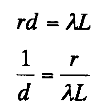
즉, 도 17의 횡축 위의 산란 벡터의 크기(1/d)는 도 15의 (A) 내지 도 15의 (E), 도 16의 (C) 및 도 16의 (E)의 전자 회절 패턴 각각에서의, 중심의 투과파의 스폿으로부터 회절파의 동심원의 패턴까지의 거리 r에 비례한다.That is, the magnitude (1 / d) of the scattering vector on the abscissa of FIG. 17 is the electron diffraction pattern of FIGS. 15A to 15E, 16C, and 16E, respectively. It is proportional to the distance r from the spot of the central transmission wave at to the pattern of the concentric circles of the diffraction wave.
즉, 도 17에 도시한 그래프에서, 3.3nm-1≤1/d≤4.1nm-1의 범위인 제1 피크는, 도 15의 (A) 내지 도 15의 (E) 및 도 16의 (A) 및 도 16의 (E)의 전자 회절 패턴의 내측의 할로 패턴의 피크 및 내측의 동심원의 패턴의 피크에 대응하고, 5.5nm-1≤1/d≤7.1nm-1의 범위인 제2 피크는 도 15의 (A) 내지 도 15의 (E) 및 도 16의 (A) 및 도 16의 (E)의 외측의 할로 패턴 및 외측의 동심원의 패턴의 피크에 대응한다.That is, in the graph shown in FIG. 17, the first peaks in the range of 3.3 nm -1 ≤ 1 / d ≤ 4.1 nm -1 are shown in FIGS. 15A to 15E and 16A. ) And the peak of the halo pattern inside the electron diffraction pattern of Fig. 16E and the peak of the concentric circle pattern, and a second peak in the range of 5.5nm -1 ≤1 / d≤7.1
도 18은 샘플 A 내지 샘플 G 각각의 제1 피크의 반값 전폭을 도시하는 그래프이고, 도 19는 샘플 A 내지 샘플 G 각각의 제2 피크의 반값 전폭을 도시하는 그래프이다. 도 18에 도시한 그래프에서, 종축은 제1 피크의 반값 전폭(FWHM)(nm-1)을 나타내고, 횡축은 샘플 A 내지 샘플 E의 산화물 반도체막 형성 시의 기판 온도(℃)를 나타낸다. 또한, 도 18의 그래프에서의 점선은 샘플 F 및 샘플 G의 제1 피크의 반값 전폭의 값을 나타낸다. 도 18의 그래프와 유사한 방식으로, 제2 피크의 반값 전폭이 도 19의 그래프에 도시된다. 도 18 및 도 19의 제1 피크 및 제2 피크의 위치(nm-1)와 반값 전폭(nm-1)을 표 1에 나열한다.18 is a graph showing the full-width half of the first peak of each of Samples A to G, and FIG. 19 is a graph showing the full-width half of the second peak of each of Samples A to G. In the graph shown in Fig. 18, the vertical axis represents the full-width (FWHM) of the first peak (nm -1 ), and the horizontal axis represents the substrate temperature (° C) when forming the oxide semiconductor films of Samples A to E. In addition, the dotted line in the graph of FIG. 18 represents the values of the full width of the half of the first peaks of Sample F and Sample G. In a manner similar to the graph of FIG. 18, the full width of the half value of the second peak is shown in the graph of FIG. The positions of the first peak and the second peak (nm -1 ) and half-width full width (nm -1 ) of FIGS. 18 and 19 are listed in Table 1.
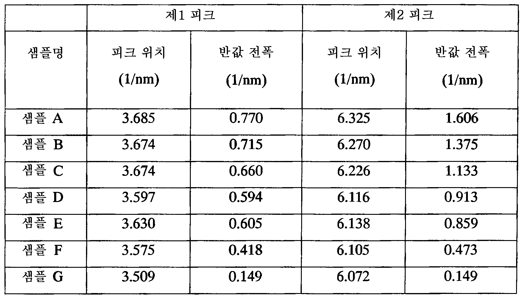
도 18 및 도 19는 산화물 반도체막의 형성 시의 기판 온도가 증가함에 따라 제1 피크 및 제2 피크 각각의 반값 전폭 및 피크 위치가 감소하는 경향을 도시한다. 또한, 제1 피크 및 제2 피크 각각의 반값 전폭이 300℃ 내지 400℃의 범위인 필름 형성 시의 기판 온도 사이에서 크게 변하지 않는 것을 도시한다. 또한, 2-단계법에 의해 형성된 샘플 F의 제1 피크 및 제2 피크 각각의 반값 전폭 및 피크 위치의 값은 샘플 A 내지 샘플 E의 반값 전폭 및 피크 위치의 값보다 작고, 단결정 상태인 샘플 G의 반값 전폭 및 피크 위치의 값보다 컸다.18 and 19 show the tendency of the half width and peak positions of the first peak and the second peak to decrease as the substrate temperature increases during the formation of the oxide semiconductor film. It is also shown that the half-width of each of the first peak and the second peak does not change significantly between the substrate temperatures at the time of film formation in the range of 300 ° C to 400 ° C. Further, the values of the half-width full width and the peak position of each of the first peak and the second peak of sample F formed by the two-step method are smaller than the values of the half-width full width and peak positions of samples A to E, and the sample G in a single crystal state It was larger than the value of half width of full width and peak position.
c축 배향의 결정 영역을 포함하는 산화물 반도체막의 결정성은 단결정 구조인 샘플 G의 결정성과는 상이하다. 따라서, c축 방향으로부터 전자빔의 조사를 행하는 전자 회절 강도 측정에서, 제1 피크 및 제2 피크 각각의 반값 전폭이 0.2nm-1이상이며, 바람직하게는 제1 피크의 반값 전폭이 0.4nm-1 이상이고, 제2 피크의 반값 전폭이 0.45nm-1 이상이다.The crystallinity of the oxide semiconductor film including the crystal region in the c-axis orientation is different from that of sample G, which is a single crystal structure. Therefore, in electron diffraction intensity measurement in which electron beam is irradiated from the c-axis direction, the full width at half of each of the first and second peaks is 0.2 nm -1 or more, and preferably the full width at half of the first peak is 0.4 nm -1. That is, the full width at half value of the second peak is 0.45 nm -1 or more.
또한, 도 13의 (A) 내지 도 13의 (E) 및 도 14의 (A) 내지 도 14의 (E)로부터, 샘플 A 및 샘플 B에서는, 즉, 성막 시의 기판 온도가 200℃ 이하로 형성된 산화물 반도체막에서는 결정성이 명료하게 관찰되지 않는다. 이를 고려하여, c축 배향의 결정 영역을 포함하는 산화물 반도체막에서는, c축 방향으로부터 전자빔의 조사를 행하는 전자 회절 강도 측정에 있어서, 제1 피크의 반값 전폭이 0.7nm-1 이하, 제2 피크의 반값 전폭이 1.4nm-1 이하인 것이 바람직하다.13A to 13E and 14A to 14E, that is, in Sample A and Sample B, that is, the substrate temperature at the time of film formation is 200 ° C. or lower. Crystallinity is not clearly observed in the formed oxide semiconductor film. In consideration of this, in an oxide semiconductor film including a crystal region of c-axis orientation, in electron diffraction intensity measurement in which electron beam is irradiated from the c-axis direction, the full width of the half of the first peak is 0.7 nm -1 or less and the second peak It is preferable that the full width of the half value of is 1.4 nm- 1 or less.
또한, 샘플 A, 샘플 E 및 샘플 G에 대해서 X선 회절(XRD: X-ray diffraction) 측정을 행하였고, 그 결과는 상술된 TEM 측정 결과를 지원한다.In addition, X-ray diffraction (XRD) measurements were performed on Sample A, Sample E, and Sample G, and the results support the TEM measurement results described above.
도 20은 면외(out-of-plane)법을 이용해서 샘플 A 및 샘플 E의 XRD 스펙트럼을 측정한 결과를 도시한다. 도 20에서, 종축은 X선 회절 강도(임의 단위)를 나타내고, 횡축은 회전각 2θ[deg.]를 나타낸다.FIG. 20 shows the results of measuring the XRD spectra of Sample A and Sample E using an out-of-plane method. In Fig. 20, the ordinate represents the X-ray diffraction intensity (arbitrary unit), and the abscissa represents the rotation angle 2θ [deg.].
도 20은 샘플 E에서 2θ가 30°근방인 영역에서 강한 피크가 관찰되지만, 샘플 A에서는 2θ가 30°근방인 영역에서 피크가 거의 관찰되지 않는 것을 도시한다. 이러한 피크는 IGZO 결정의 (009)면에서의 회절에 기인한다. 이는 또한 샘플 E가 c축 배향의 결정 영역을 포함하는 산화물 반도체막으로서, 비정질 구조를 갖는 샘플 A와는 명확히 상이하다는 것을 나타낸다.20 shows that in Sample E, a strong peak was observed in the region where 2θ is around 30 °, but in Sample A, a peak was hardly observed in the region where 2θ was around 30 °. This peak is due to diffraction in the (009) plane of the IGZO crystal. This also shows that Sample E is an oxide semiconductor film containing a crystal region of c-axis orientation, and is clearly different from Sample A having an amorphous structure.
도 21의 (A)는 면내(in-plane)법을 이용해서 샘플 E의 XRD 스펙트럼을 측정한 결과를 도시한다. 유사하게, 도 21의 (B)는 면내법을 이용해서 샘플 G의 XRD 스펙트럼을 측정한 결과를 도시한다. 도 21의 (A) 및 도 21의 (B)에서, 종축은 X선 회절 강도(임의 단위)를 나타내고, 횡축은 회전각 φ[deg.]를 나타낸다. 본 실시예에서 이용된 면내법에서는, 샘플의 c축 방향을 회전의 축으로 이용해서 샘플을 회전각 φ로 회전시켜 XRD 측정을 행하였다.21 (A) shows the result of measuring the XRD spectrum of Sample E using an in-plane method. Similarly, FIG. 21 (B) shows the result of measuring the XRD spectrum of Sample G using an in-plane method. In Figs. 21A and 21B, the ordinate represents the X-ray diffraction intensity (arbitrary unit), and the abscissa represents the rotation angle phi [deg.]. In the in-plane method used in this example, XRD measurement was performed by rotating the sample at a rotation angle φ using the c-axis direction of the sample as an axis of rotation.
도 21의 (B)에 도시한 샘플 G의 XRD 스펙트럼에서, 피크는 회전각인 60°의 등간격으로 관찰되며, 이는 샘플 G가 6회 대칭성을 갖는 단결정막인 것을 도시한다. 한편, 도 21의 (A)에 도시한 샘플 E의 XRD 스펙트럼에서는 규칙적인 피크가 관찰되지 않으며, 이는, 결정 영역의 a-b면 방향으로의 배향은 존재하지 않음을 나타낸다. 즉, 샘플 E의 각각의 결정 영역은 c축을 따라 결정화되지만, a-b면을 따른 배향이 반드시 나타나는 것은 아니다. 이는 또한, 샘플 E는 c축 배향의 결정 영역을 포함하는 산화물 반도체막으로서, 단결정 구조인 샘플 G와는 명확히 상이하다는 것을 나타낸다.In the XRD spectrum of sample G shown in Fig. 21B, peaks are observed at equal intervals of a rotation angle of 60 °, which shows that sample G is a single crystal film having six symmetries. On the other hand, a regular peak was not observed in the XRD spectrum of Sample E shown in Fig. 21A, indicating that there was no orientation of the crystal region in the a-b plane direction. That is, each crystal region of Sample E crystallizes along the c-axis, but the orientation along the a-b plane does not necessarily appear. This also shows that Sample E is an oxide semiconductor film containing a crystal region of c-axis orientation, and is clearly different from Sample G, which is a single crystal structure.
상술한 바와 같이, 본 발명의 실시예에 따른 c축 배향의 결정 영역을 포함하는 산화물 반도체막은, 비정질 구조의 산화물 반도체막의 결정성 및 단결정 구조의 산화물 반도체막의 결정성과는 명확히 상이한 결정성을 갖는다.As described above, the oxide semiconductor film including the c-axis oriented crystal region according to the embodiment of the present invention has crystallinity that is clearly different from the crystallinity of the oxide semiconductor film having an amorphous structure and the crystallinity of the oxide semiconductor film having a single crystal structure.
상술한 바와 같이 c축 배향의 결정 영역을 포함하는 산화물 반도체막은 전체가 비정질인 산화물 반도체막과 비교해서 양호한 결정성을 갖고, 산소 결함으로 대표되는 결함, 또는 댕글링 본드 등에 결합되는 수소 등의 불순물이 저감된다. 산소 결함으로 대표되는 결함, 댕글링 본드 등에 결합되는 수소 등은 산화물 반도체막의 캐리어 공급원으로 기능하여, 산화물 반도체막의 전기 전도도를 변화시킬 수 있다. 따라서, 그러한 결함이 저감되어 있는 결정 영역을 포함하는 산화물 반도체막은 전기 전도도가 안정되어 있고, 가시광, 자외광 등의 조사에 대하여 보다 전기적으로 안정되어 있다. 그러한 결정 영역을 포함하는 산화물 반도체막을 트랜지스터에 이용함으로써, 전기적 특성이 안정되고 신뢰성이 높은 반도체 장치를 제공할 수 있다.As described above, the oxide semiconductor film including a c-axis oriented crystal region has good crystallinity compared to an amorphous oxide semiconductor film as a whole, and is a defect represented by an oxygen defect, or an impurity such as hydrogen bonded to a dangling bond or the like. This is reduced. Defects represented by oxygen defects, hydrogen bonded to dangling bonds, or the like function as a carrier source of the oxide semiconductor film, and thus can change the electrical conductivity of the oxide semiconductor film. Therefore, the oxide semiconductor film including a crystal region in which such defects are reduced is stable in electrical conductivity and more electrically stable in the irradiation with visible light, ultraviolet light, and the like. By using an oxide semiconductor film containing such a crystal region for a transistor, a semiconductor device with stable electrical characteristics and high reliability can be provided.
<2.ESR 측정><2.ESR measurement>
이 부분에서는, 상기의 실시예에 따라 산화물 반도체막을 형성하였고, 산화물 반도체막을 전자 스핀 공명(ESR: Electron Spin Resonance)법을 이용해서 평가하였다. 그 결과는 이하에 설명한다.In this part, an oxide semiconductor film was formed according to the above-described examples, and the oxide semiconductor film was evaluated using an electron spin resonance (ESR) method. The results are described below.
이 부분에서는, 스퍼터링법에 의해 석영 기판 위에 산화물 반도체막을 형성한 샘플 H와, 산화물 반도체막을 형성한 석영 기판에 가열 처리를 행하여 얻어진 샘플 I를 제조하였다. 산화물 반도체막을 형성하기 위한 타겟은, In2O3:Ga2O3:ZnO=1:1:2 [몰수비]의 조성비를 갖는다. 이외의 조건은 이하와 같았다: 성막 가스 흐름에 대해서, 아르곤 가스의 흐름은 30sccm이고 산소 가스의 흐름은 15sccm이고, 성막 시의 기판 온도는 400℃이고, 압력은 0.4Pa이고, 기판과 타겟간 거리는 60mm이고, 무선 주파수(RF) 전력은 0.5kW이고, 막 두께는 100nm였다.In this part, Sample H obtained by heating the quartz substrate on which the oxide semiconductor film was formed on the quartz substrate and the quartz substrate on which the oxide semiconductor film was formed by sputtering were prepared. The target for forming the oxide semiconductor film has a composition ratio of In 2 O 3 : Ga 2 O 3 : ZnO = 1: 1: 2 [molar ratio]. Other conditions were as follows: For the deposition gas flow, the flow of argon gas was 30 sccm, the flow of oxygen gas was 15 sccm, the substrate temperature at the time of deposition was 400 ° C., the pressure was 0.4 Pa, and the distance between the substrate and the target was It was 60 mm, the radio frequency (RF) power was 0.5 kW, and the film thickness was 100 nm.
산화물 반도체막을 형성한 후에, 산화물 반도체막을 형성한 석영 기판에 가열 처리를 행해서, 샘플 I를 형성하였다. 가열 처리는 노점 -24℃의 건조 분위기에서 온도 450℃로 1시간 동안 행하였다. 이러한 방식으로, 산화물 반도체막을 석영 기판 위에 각각 형성한 샘플 H 및 샘플 I를 제조하였다.After the oxide semiconductor film was formed, heat treatment was performed on the quartz substrate on which the oxide semiconductor film was formed to form Sample I. The heat treatment was performed for 1 hour at a temperature of 450 ° C in a dry atmosphere at a dew point of -24 ° C. In this way, Sample H and Sample I, each of which formed an oxide semiconductor film on a quartz substrate, were prepared.
이 부분에서, 샘플 H 및 샘플 I에 대해서 행한 ESR 측정을 설명한다. ESR 측정은 제만(Zeeman) 효과를 이용하여 물질 내의 고립 전자를 측정한 방법이다. 샘플에 특정한 진동수 ν의 마이크로파를 조사하면서, 샘플에 인가된 자장 H가 소인(swept)되는 경우에, 특정한 자장 H에 있어서 샘플 내의 고립 전자가 마이크로파를 흡수하고, 자장에 평행한 스핀 에너지 준위로부터 자장에 반 평행한 스핀 에너지 준위로의 천이가 일어난다. 샘플 내의 고립 전자에 의해 흡수되는 마이크로파의 진동수 ν와 샘플에 인가된 자장 H 간의 관계는 이하의 수학식으로 표현될 수 있다.In this section, ESR measurements performed on Sample H and Sample I will be described. ESR measurement is a method of measuring isolated electrons in a material using the Zeman effect. When the magnetic field H applied to the sample is swept while irradiating microwaves of a specific frequency ν to the sample, in the specific magnetic field H, isolated electrons in the sample absorb the microwaves, and the magnetic field from the spin energy level parallel to the magnetic field The transition to the spin energy level occurs in antiparallel to. The relationship between the frequency ν of the microwaves absorbed by the isolated electrons in the sample and the magnetic field H applied to the sample can be expressed by the following equation.

수학식 2에서, h는 플랑크 상수를 나타내고, μB는 보어 마그네톤을 나타낸다. 또한, g는 g값이라 불리는 계수이며, 물질 내의 고립 전자에 인가된 국소 자장에 따라 변화한다; 즉, 상기의 수학식 2를 이용해서 g값을 계산함으로써, 댕글링 본드 등의 고립 전자의 환경을 알 수 있다.In
본 예에서, ESR 측정은 브루커(Bruker)사 제조의 E500을 이용해서 행하였다. 측정 조건은 이하와 같았다: 측정 온도는 실온이고, 마이크로파 주파수는 9.5GHz이고, 마이크로파 전력은 0.2mW였다.In this example, ESR measurement was performed using E500 manufactured by Bruker. The measurement conditions were as follows: the measurement temperature was room temperature, the microwave frequency was 9.5 GHz, and the microwave power was 0.2 mW.
샘플 H 및 샘플 I에 대해서, ESR 측정을 행한 결과를 도 22에 도시한다. 도 22에 도시한 그래프에서, 종축은 마이크로파의 흡수 강도의 1차 미분을 나타내고, 횡축은 g값을 나타낸다.The results of ESR measurements for Sample H and Sample I are shown in FIG. 22. In the graph shown in Fig. 22, the vertical axis represents the first derivative of the absorption intensity of microwaves, and the horizontal axis represents the g value.
도 22의 그래프에 도시한 바와 같이, 샘플 I에서는 마이크로파의 흡수에 대응하는 신호는 관측되지 않았지만, 샘플 H에서는 g값이 1.93 근방인 영역에서 마이크로파의 흡수에 대응하는 신호가 관찰되었다. g값이 1.93 근방인 영역에서의 신호의 적분값을 계산함으로써, 마이크로파의 흡수에 대응하는 고립 전자의 스핀 밀도, 즉 1.3×10¹⁸(spins/cm3)의 스핀 밀도가 얻어질 수 있다. 샘플 I에서는, 마이크로파의 흡수가 검출 하한보다 낮아서, 샘플 I의 고립 전자의 스핀 밀도는 1×10¹⁶(spins/cm3) 이하인 점에 주목한다.As shown in the graph of FIG. 22, in Sample I, a signal corresponding to the absorption of microwaves was not observed, but in Sample H, a signal corresponding to the absorption of microwaves was observed in the region where the g value was near 1.93. By calculating the integral value of the signal in the region where the g value is near 1.93, a spin density of isolated electrons corresponding to absorption of microwaves, that is, a spin density of 1.3 × 10 18 (spins / cm 3 ) can be obtained. Note that in Sample I, the absorption of microwaves was lower than the lower detection limit, and the spin density of the isolated electrons of Sample I was 1 × 10 16 (spins / cm3) or less.
본 명세서에서, In-Ga-Zn-O계 산화물 반도체막에서 g값이 1.93 근방인 신호가 어떤 종류의 댕글링 본드에 귀속될지를 조사하기 위해서 양자 화학 계산을 행하였다. 구체적으로, 금속 원자가 산소 결함에 대응하는 댕글링 본드를 갖는 클러스터(cluster) 모델을 형성하고, 클러스터 모델의 구조를 최적화하여, 그 g값을 계산하였다.In the present specification, quantum chemical calculations were performed to investigate what kind of dangling bond a signal having a g value of around 1.93 in an In—Ga—Zn—O-based oxide semiconductor film. Specifically, a cluster model in which a metal atom has a dangling bond corresponding to an oxygen defect was formed, and the structure of the cluster model was optimized to calculate its g value.
모델의 구조를 최적화하고 구조가 최적화된 모델의 g값을 계산하기 위해 ADF(Amsterdam Density Functional) 소프트웨어를 이용하였다. 또한, 모델의 구조의 최적화 및 구조가 최적화된 모델의 g값의 계산 모두에 있어서 범함수로서 GGA:BP를 이용했고, 기저함수로서 TZ2P를 이용하였다. 또한, 코어형(Core Type)으로서, 모델의 구조의 최적화에는 Large를 이용했고, g값의 계산에는 None을 이용하였다.ADF (Amsterdam Density Functional) software was used to optimize the structure of the model and to calculate the g value of the model with the optimized structure. In addition, GGA: BP was used as the general function and TZ2P was used as the base function in both the optimization of the structure of the model and the calculation of the g value of the model in which the structure was optimized. In addition, as the core type, large was used to optimize the structure of the model, and None was used to calculate the g value.
도 23은 상기의 양자 화학 계산에 의해 얻어진 In-Ga-Zn-O계 산화물 반도체막에서의 댕글링 본드의 모델을 도시한다. 도 23은, 인듐-산소 결합의 산소 결함에 의한 댕글링 본드(g=1.984), 갈륨-산소 결합의 산소 결함에 의한 댕글링 본드(g=1.995) 및 아연-산소 결합의 산소 결함에 의한 댕글링 본드(g=1.996)를 도시한다. 이들 댕글링 본드의 g값은, 샘플 H의 마이크로파의 흡수에 대응하는 신호의g값(=1.93)에 비교적 가깝다. 즉, 샘플 H는 인듐, 갈륨 또는 아연 중 하나 이상과 산소와의 결합에서 산소 결함이 발생할 가능성을 갖는다.23 shows a model of dangling bond in an In-Ga-Zn-O-based oxide semiconductor film obtained by the above quantum chemical calculation. FIG. 23 shows dangling bonds due to oxygen defects of indium-oxygen bonds (g = 1.984), dangling bonds due to oxygen defects of gallium-oxygen bonds (g = 1.995), and dangling due to oxygen defects of zinc-oxygen bonds. The ring bond (g = 1.996) is shown. The g value of these dangling bonds is relatively close to the g value (= 1.93) of the signal corresponding to the absorption of microwaves in sample H. That is, Sample H has the potential to cause oxygen defects in the combination of oxygen with one or more of indium, gallium or zinc.
그러나, 샘플 I에 있어서는 g값이 1.93 근방인 영역에서 마이크로파의 흡수에 대응하는 신호가 관찰되지 않는다. 이는 산화물 반도체막이 형성된 후에 건조 분위기에서 가열 처리를 행함으로써, 산소 결함에 산소가 부가되는 것을 나타낸다. 상기의 실시예에서 설명된 바와 같이, 산화물 반도체막의 산소 결함은 전기 전도도를 변화시키는 캐리어로서 기능할 수 있어, 산소 결함을 저감하여, 산화물 반도체막을 포함하는 트랜지스터의 신뢰성을 향상시킬 수 있다.However, in Sample I, a signal corresponding to absorption of microwaves is not observed in the region where the g value is near 1.93. This indicates that oxygen is added to the oxygen defect by performing heat treatment in a dry atmosphere after the oxide semiconductor film is formed. As described in the above embodiment, the oxygen defect of the oxide semiconductor film can function as a carrier for changing the electrical conductivity, thereby reducing the oxygen defect and improving the reliability of the transistor including the oxide semiconductor film.
따라서, 본 발명의 실시예에 따른, c축 배향의 결정 영역을 포함하는 산화물 반도체막에서, 산화 반도체막이 형성된 후에 가열 처리를 행함으로써 산소 결함에 산소를 부가하는 것이 바람직하고, ESR 측정에서, g값이 1.93 근방인 영역에서의 스핀 밀도는 1.3×10¹⁸(spins/cm3) 이하인 것이 바람직하고, 1×10¹⁶(spins/cm3) 이하인 것이 보다 바람직하다.Therefore, in the oxide semiconductor film including the c-axis oriented crystal region according to the embodiment of the present invention, it is preferable to add oxygen to the oxygen defect by performing heat treatment after the oxide semiconductor film is formed, and in ESR measurement, g The spin density in the region near the value of 1.93 is preferably 1.3 × 10 18 (spins / cm 3 ) or less, and more preferably 1 × 10 16 (spins / cm 3 ) or less.
<3. 저온 PL 측정><3. Low temperature PL measurement>
이 부분에서, 상기의 실시예에 따라 산화물 반도체막을 형성하고, 산화물 반도체막을 저온 포토루미네센스(PL: photoluminescence) 측정을 이용해서 평가한다. 그 결과에 대해 이하에 설명한다.In this part, an oxide semiconductor film is formed according to the above embodiment, and the oxide semiconductor film is evaluated using low temperature photoluminescence (PL) measurements. The results will be described below.
이 부분에서, 스퍼터링법에 의해 성막 시의 기판 온도 200℃로 석영 기판 위에 산화물 반도체막을 형성한 샘플 J와, 스퍼터링법에 의해 성막 시의 기판 온도 400℃로 석영 기판 위에 산화물 반도체막을 형성한 샘플 K를 제조하였다. 즉, 샘플 J는 c축 배향의 결정 영역을 포함하지 않는 산화물 반도체막이며, 샘플 K는 c축 배향의 결정 영역을 포함하는 산화물 반도체막이다. 산화물 반도체막을 형성하기 위한 타겟은 In2O3:Ga2O3:ZnO=1:1:2 [몰수비]의 조성비를 갖는다. 이외의 조건은 이하와 같았다. 성막 가스 흐름에 대해서, 아르곤 가스의 흐름은 30sccm이고, 산소 가스의 흐름은 15sccm이고, 압력은 0.4Pa이고, 기판과 타겟간 거리는 60mm이고, 무선 주파수(RF) 전원은 0.5kW이고, 막 두께 100nm였다.In this part, sample J in which an oxide semiconductor film is formed on a quartz substrate at a substrate temperature of 200 ° C during film formation by sputtering, and sample K in which an oxide semiconductor film is formed on a quartz substrate at a substrate temperature of 400 ° C during film formation by sputtering method. Was prepared. That is, sample J is an oxide semiconductor film that does not include a c-axis-oriented crystal region, and sample K is an oxide semiconductor film that includes a c-axis-oriented crystal region. The target for forming the oxide semiconductor film has a composition ratio of In 2 O 3 : Ga 2 O 3 : ZnO = 1: 1: 2 [molar ratio]. Other conditions were as follows. For the deposition gas flow, the flow of argon gas was 30 sccm, the flow of oxygen gas was 15 sccm, the pressure was 0.4 Pa, the distance between the substrate and the target was 60 mm, the radio frequency (RF) power source was 0.5 kW, and the film thickness was 100 nm. It was.
또한, 산화물 반도체막이 형성된 후에, 샘플 J 및 샘플 K 각각에 있어서, 산화물 반도체막을 형성한 석영 기판에 가열 처리를 행하였다. 가열 처리는 노점 -24℃의 건조 분위기에서 온도 450℃로 1시간 동안 행하였다. 이러한 방식으로, 산화물 반도체막을 석영 기판 위에 각각 형성한 샘플 J 및 샘플 K를 제조하였다.In addition, after the oxide semiconductor film was formed, in each of Sample J and Sample K, heat treatment was performed on the quartz substrate on which the oxide semiconductor film was formed. The heat treatment was performed for 1 hour at a temperature of 450 ° C in a dry atmosphere at a dew point of -24 ° C. In this way, Sample J and Sample K, each of which formed an oxide semiconductor film on a quartz substrate, were prepared.
이 부분에서, 샘플 J 및 샘플 K에 대해서, 저온 PL 측정을 행한다. 저온 PL 측정에서, 극저온 분위기에서 여기 광을 샘플에 조사해서 샘플에 에너지를 부여하고, 샘플에 전자와 정공(hole)이 생성되면서, 여기 광의 조사가 정지하고, 여기 광 조사에 의해 생성된 전자와 정공이 재결합하여 야기된 광 방출을 CCD(Charge Coupled Device) 등을 이용해서 검출한다.In this part, low-temperature PL measurement is performed on Sample J and Sample K. In the low temperature PL measurement, excitation light is irradiated to the sample in a cryogenic atmosphere to impart energy to the sample, electrons and holes are generated in the sample, and irradiation of excitation light stops, and electrons generated by excitation light irradiation Light emission caused by recombination of holes is detected using a CCD (Charge Coupled Device) or the like.
본 예에서, 저온 PL 측정은 헬륨 가스 분위기에서 측정 온도 10K로 행하였다. 여기 광에 대해서, He-Cd 가스 레이저로부터 방출된 325nm의 파장을 갖는 광을 이용하였다. 또한, 광 방출을 검출하기 위해 CCD를 이용하였다.In this example, the low temperature PL measurement was performed at a measurement temperature of 10K in a helium gas atmosphere. For the excitation light, light having a wavelength of 325 nm emitted from a He-Cd gas laser was used. In addition, a CCD was used to detect light emission.
저온 PL 측정에서 검출된 샘플 J 및 샘플 K의 발광 스펙트럼을 도 24에 도시한다. 도 24에 도시한 그래프에서 종축은 PL 검출 카운트(counts)를 나타내고, 횡축은 검출된 광 방출의 에너지(eV)를 나타낸다.The emission spectra of Sample J and Sample K detected in the low temperature PL measurement are shown in FIG. 24. In the graph shown in Fig. 24, the ordinate represents the PL detection counts, and the abscissa represents the energy (eV) of the detected light emission.
도 24의 그래프에 따르면, 샘플 J 및 샘플 K 각각은 발광 에너지가 1.8eV 근방인 영역에서 피크를 갖지만, 샘플 K의 PL 검출 카운트수가 샘플 J보다 대략 100만큼 작다. 샘플 J 및 샘플 K 각각에 있어서 발광 에너지가 3.2eV 근방인 영역에서의 피크는, 저온 PL 측정 장치의 석영창(quartz window)에 기인한다.According to the graph of FIG. 24, each of sample J and sample K has a peak in the region where the luminescence energy is around 1.8 eV, but the number of PL detection counts of sample K is about 100 smaller than that of sample J. The peak in the region in which the luminescence energy in each of Sample J and Sample K is 3.2 eV is due to the quartz window of the low-temperature PL measuring apparatus.
본 명세서에서, 도 24의 그래프에서 발광 에너지가 1.8eV 근방인 영역에서의 피크는 산화물 반도체막의 밴드 구조에서 전도대의 하부로부터 대략 1.8eV의 깊이에 에너지 준위가 존재하는 것을 나타낸다. 이러한 밴드갭의 깊은 에너지 준위는 도 3의 전자 상태 밀도의 계산 결과에서의 산소 결함에 기인하는 트랩 준위와 부합된다. 따라서, 도 24의 그래프에서 발광 에너지가 1.8eV 근방인 영역에서의 발광 피크는 도 4의 밴드 다이어그램에서의 산소 결함에 기인하는 트랩 준위의 에너지 준위를 나타낸다고 가정할 수 있다. 즉, 샘플 K에 있어서 발광 에너지가 1.8eV 근방인 영역에서의 PL 검출 카운트수가 샘플 J보다 작기 때문에, c축 배향의 결정 영역을 포함하는 산화물 반도체막에서, 산소 결함에 기인하는 트랩 준위의 수, 즉, 산소 결함의 수가 저감된다고 가정한다.In the present specification, in the graph of FIG. 24, the peak in the region where the emission energy is near 1.8 eV indicates that an energy level exists at a depth of approximately 1.8 eV from the lower portion of the conduction band in the band structure of the oxide semiconductor film. The deep energy level of this bandgap is consistent with the trap level due to oxygen defects in the calculation result of the electron state density in FIG. 3. Therefore, it can be assumed in the graph of FIG. 24 that the emission peak in the region where the emission energy is around 1.8 eV represents the energy level of the trap level due to the oxygen defect in the band diagram of FIG. 4. That is, in the sample K, since the number of PL detection counts in the region where the emission energy is near 1.8 eV is smaller than the sample J, the number of trap levels due to oxygen defects in the oxide semiconductor film including the crystal region in the c-axis orientation, That is, it is assumed that the number of oxygen defects is reduced.
<4. 부바이어스 스트레스 광열화 측정><4. Bubias stress photodegradation measurement>
본 예에서, 상기의 실시예에 따라 산화물 반도체막을 포함한 트랜지스터를 제조하고, 트랜지스터에 광을 조사하면서 트랜지스터의 게이트에 부전압을 인가해서 트랜지스터에 스트레스를 부여함으로써, 트랜지스터의 임계 전압이 스트레스를 부여한 시간의 길이에 따라 변하였다. 트랜지스터의 임계 전압의 변화를 평가한 결과에 대해서 설명한다. 이러한 스트레스로 인한 트랜지스터의 임계 전압 등의 변화를 부바이어스 스트레스 광열화라고 한다.In this example, the time for which the threshold voltage of the transistor is stressed by manufacturing the transistor including the oxide semiconductor film according to the above embodiment and applying a negative voltage to the gate of the transistor while irradiating light to the transistor to stress the transistor. It changed according to the length of. The result of evaluating the change in the threshold voltage of the transistor will be described. The change in the threshold voltage of the transistor due to the stress is called negative bias stress photodeterioration.
이 부분에서, 상기의 실시예에서 설명된 c축 배향의 결정 영역이 형성된 산화물 반도체막이 설치된 트랜지스터(샘플 L)를 제조하였다. 또한, 비교예로서 샘플 L과 유사한 재료로 형성되지만, c축 배향의 결정 영역이 형성되지 않은 산화물 반도체막이 설치된 트랜지스터(샘플 M)를 제조하였다. 그 후, 샘플 L 및 샘플 M에 광을 조사하면서 샘플의 게이트에 부 전압을 인가해서 샘플 L 및 샘플 M에 스트레스를 부여하여, 스트레스를 부여한 시간의 길이에 따라 변화되는 샘플 L 및 샘플 M의 임계 전압 Vth를 평가하였다. 샘플 L 및 샘플 M의 제조 방법에 대해서 이하에 설명한다.In this part, a transistor (sample L) in which an oxide semiconductor film in which a crystal region having a c-axis orientation described in the above example is formed is formed was manufactured. Further, as a comparative example, a transistor (sample M) having an oxide semiconductor film formed of a material similar to sample L but not having a c-axis oriented crystal region was prepared. Subsequently, while irradiating light to Samples L and M, a negative voltage is applied to the gates of the samples to stress Samples L and M, and the thresholds of Samples L and M change according to the length of the stressed time. The voltage Vth was evaluated. The manufacturing method of sample L and sample M is demonstrated below.
우선, 플라즈마 CVD법에 의해, 하지막(base film)으로서 두께 100nm의 질화 실리콘막 및 두께 150nm의 산화 질화 실리콘막을 연속해서 글래스 기판 위에 형성하고, 그 후 산화 질화 실리콘막 위에 스퍼터링법에 의해 두께 100nm의 텅스텐 막을 형성하였다. 텅스텐 막을 선택적으로 에칭함으로써, 테이퍼(tapered) 형상을 갖는 게이트 전극을 형성하였다. 그 후, 플라즈마 CVD법에 의해 게이트 절연막으로서 게이트 전극 위에 두께 100nm의 산화 질화 실리콘막을 형성하였다.First, by a plasma CVD method, a silicon nitride film with a thickness of 100 nm and a silicon nitride oxide film with a thickness of 150 nm are successively formed on a glass substrate as a base film, and thereafter, a thickness of 100 nm by sputtering on the silicon nitride film. A tungsten film was formed. By selectively etching the tungsten film, a gate electrode having a tapered shape was formed. Thereafter, a silicon oxynitride film having a thickness of 100 nm was formed on the gate electrode as a gate insulating film by plasma CVD.
다음으로, 스퍼터링법에 의해 게이트 절연막 위에 산화물 반도체막을 형성하였다. 샘플 L의 산화물 반도체막은, 시드 결정으로서 기능하는 두께 5nm의 산화물 반도체막 위에, 두께 30nm의 산화물 반도체막을 적층하고, 가열 처리를 행하여 c축 배향의 결정 영역을 형성하는 방식으로 형성되었다. 샘플 M의 산화물 반도체막은 두께 25nm의 산화물 반도체막에 가열 처리를 행하는 방식으로 형성되었다.Next, an oxide semiconductor film was formed on the gate insulating film by sputtering. The oxide semiconductor film of Sample L was formed in such a way that a 30 nm-thick oxide semiconductor film was laminated on a 5 nm-thick oxide semiconductor film functioning as a seed crystal, and subjected to heat treatment to form a c-axis oriented crystal region. The oxide semiconductor film of Sample M was formed by heating the oxide semiconductor film with a thickness of 25 nm.
우선, 샘플 L의 산화물 반도체막의 제조 방법에 대해서 설명한다. 시드 결정으로서 기능하는 산화물 반도체막은 스퍼터링법에 의해 형성되고, 산화물 반도체막을 형성하기 위한 타겟으로서, In2O3:Ga2O3:ZnO=1:1:2 [몰수비]의 조성비를 갖는 타겟을 이용하였다. 이외의 형성 조건은 이하와 같았다: 성막 시의 기판 온도는 200℃이고, 성막 가스 흐름율에서 산소 가스는 50%이고, 아르곤 가스는 50%이고, 압력은 0.6Pa이고, 기판과 타겟간 거리는 100mm이고, 직류(DC) 전력은 5kW이고, 막 두께는 5nm였다. 산화물 반도체막이 형성된 후에, 질소 분위기에서 온도 450℃로 1시간 동안 가열 처리를 행하여, 시드 결정으로서 기능하는 산화물 반도체막을 결정화하였다. 그 후, 시드 결정으로서 기능하는 산화물 반도체막 위에, 스퍼터링법에 의해 두께 30nm의 산화물 반도체막을, 시드 결정으로서 기능하는 산화물 반도체막을 형성하는 조건과 유사한 조건 하에서 형성하였다. 또한, 오븐을 이용해서 질소 분위기에서 온도 450℃로 1시간 동안 가열 처리를 행하고, 또한 질소와 산소의 혼합 분위기에서 온도 450℃로 1시간 동안 가열 처리를 행하여, c축 배향의 결정 영역을 포함한 산화물 반도체막을 형성하였다.First, a method for manufacturing the oxide semiconductor film of Sample L will be described. An oxide semiconductor film that functions as a seed crystal is formed by a sputtering method, and is a target for forming an oxide semiconductor film, a target having a composition ratio of In 2 O 3 : Ga 2 O 3 : ZnO = 1: 1: 2 [molar ratio] Was used. The other forming conditions were as follows: The substrate temperature at the time of film formation was 200 ° C, the oxygen gas at the film formation gas flow rate was 50%, the argon gas was 50%, the pressure was 0.6 Pa, and the distance between the substrate and the target was 100 mm. , DC power was 5 kW, and the film thickness was 5 nm. After the oxide semiconductor film was formed, heat treatment was performed at a temperature of 450 ° C. for 1 hour in a nitrogen atmosphere to crystallize the oxide semiconductor film functioning as a seed crystal. Thereafter, an oxide semiconductor film having a thickness of 30 nm was formed on the oxide semiconductor film functioning as a seed crystal under conditions similar to the conditions for forming an oxide semiconductor film functioning as a seed crystal. In addition, an oxide containing a crystal region in the c-axis orientation was subjected to heat treatment for 1 hour at a temperature of 450 ° C in a nitrogen atmosphere using an oven, and for 1 hour at a temperature of 450 ° C in a mixed atmosphere of nitrogen and oxygen. A semiconductor film was formed.
또한, 스퍼터링법에 의해 샘플 M의 산화물 반도체막이 형성되었고, 산화물 반도체막을 형성하기 위한 타겟으로서, In2O3:Ga2O3:ZnO=1:1:2 [몰수비]의 조성비를 갖는 타겟을 이용하였다. 이외의 조건은 이하와 같았다: 성막 시의 기판 온도는 200℃이고, 성막 가스 흐름율에서 산소 가스는 50%이고, 아르곤 가스는 50%이고, 압력은 0.6Pa이고, 기판과 타겟간 거리는 100mm이고, 직류(DC) 전력은 5kW이고, 막 두께는 25nm였다. 산화물 반도체막이 형성된 후에, RTA(Rapid Thermal Annealing)법을 이용해서 질소 분위기에서 온도 650℃로 6분 동안 가열 처리를 행하였다. 또한, 오븐을 이용해서 질소와 산소의 혼합 분위기에서 온도 450℃로 1시간 동안 가열 처리를 행하여, c축 배향의 결정 영역을 포함하지 않은 산화물 반도체막을 형성하였다.Further, an oxide semiconductor film of Sample M was formed by sputtering, and as a target for forming the oxide semiconductor film, a target having a composition ratio of In 2 O 3 : Ga 2 O 3 : ZnO = 1: 1: 2 [molar ratio] Was used. Other conditions were as follows: The substrate temperature at the time of film formation was 200 ° C, the oxygen gas at the film formation gas flow rate was 50%, the argon gas was 50%, the pressure was 0.6 Pa, and the distance between the substrate and the target was 100 mm. , DC (DC) power is 5kW, the film thickness was 25nm. After the oxide semiconductor film was formed, heat treatment was performed for 6 minutes at a temperature of 650 ° C. in a nitrogen atmosphere using a Rapid Thermal Annealing (RTA) method. Further, an oven was used for 1 hour in a mixed atmosphere of nitrogen and oxygen at a temperature of 450 ° C. for 1 hour to form an oxide semiconductor film containing no crystal region in c-axis orientation.
다음으로, 산화물 반도체막 위에, 티탄막, 알루미늄막, 티탄막을 적층한 도전막을 스퍼터링법을 이용해서 형성하고 도전막을 선택적으로 에칭하여 소스 전극 및 드레인 전극을 형성하였다. 그 후, 제1 층간 절연막으로서 두께 400nm의 산화 실리콘막을 형성하였다. 또한, 제2 층간 절연막으로서 두께 1.5μm의 아크릴 수지로 형성되는 절연막을 형성하였다. 마지막으로, 질소 분위기에서 온도 250℃로 1시간 동안 가열 처리를 행하여, 샘플 L 및 샘플 M을 제조하였다.Next, a conductive film obtained by laminating a titanium film, an aluminum film, and a titanium film on an oxide semiconductor film was formed using a sputtering method, and the conductive film was selectively etched to form a source electrode and a drain electrode. Thereafter, a silicon oxide film having a thickness of 400 nm was formed as the first interlayer insulating film. Further, an insulating film formed of an acrylic resin having a thickness of 1.5 μm was formed as the second interlayer insulating film. Finally, heat treatment was performed at a temperature of 250 ° C. for 1 hour in a nitrogen atmosphere to prepare Sample L and Sample M.
그 후, 샘플 L 및 샘플 M에 광을 조사하면서 샘플의 게이트에 부 전압을 인가하여 샘플 L 및 샘플 M에 스트레스를 부여하고, 스트레스를 부여한 시간의 길이에 따른 샘플 L 및 샘플 M의 Id-Vg 특성을 측정하여, 스트레스를 부여한 전후의 임계 전압의 변화량을 얻었다.Then, while irradiating light to Sample L and Sample M, a negative voltage is applied to the gate of the sample to stress Sample L and Sample M, and the Id-Vg of Sample L and Sample M along the length of the stressed time The characteristics were measured to obtain the amount of change in the threshold voltage before and after applying stress.
스트레스는 실온의 대기 분위기에서 이하의 조건 하에서 부여되었다: 게이트 전압은 -20V이고, 드레인 전압은 0.1V이고, 소스 전압은 0V이고, 조사에 이용된 광의 조도는 36000(lx)이었다. 스트레스를 부여한 시간의 길이를, 100초, 300초, 600초, 1000초, 1800초, 3600초, 7200초, 10000초, 18000초 및 43200초(12시간)로 변경함으로써 샘플 L 및 샘플 M의 Id-Vg 특성을 측정하였다. Id-Vg 특성을 측정할 때, 드레인 전압을 +10V로 설정하고, 게이트 전압을 -10V로부터 +10V의 범위에서 소인하고, 이외의 조건은 스트레스를 부여할 때의 조건과 유사하였다.The stress was imparted under the following conditions in an atmospheric atmosphere at room temperature: the gate voltage was -20 V, the drain voltage was 0.1 V, the source voltage was 0 V, and the illuminance of light used for irradiation was 36000 (lx). By changing the length of the stressed time to 100 seconds, 300 seconds, 600 seconds, 1000 seconds, 1800 seconds, 3600 seconds, 7200 seconds, 10000 seconds, 18000 seconds and 43200 seconds (12 hours), Id-Vg properties were measured. When measuring the Id-Vg characteristic, the drain voltage was set to + 10V, the gate voltage was sweeped in the range of -10V to + 10V, and the other conditions were similar to those under stress.
도 25는 샘플 L 및 샘플 M의 임계 전압의 변화량을 도시하는 그래프이다. 도 25에 도시한 그래프에서 종축은 임계 전압의 변화량 ΔVth(V)를 나타내고, 횡축은 스트레스 시간(sec)을 나타낸다.25 is a graph showing the amount of change in the threshold voltages of Sample L and Sample M. In the graph shown in FIG. 25, the vertical axis represents the change amount ΔVth (V) of the threshold voltage, and the horizontal axis represents the stress time (sec).
도 25에서, 샘플 L의 임계 전압의 변화량 ΔVth는 최대 대략 -1V인 반면, 샘플 M의 임계 전압의 변화량 ΔVth은 최대 대략 -2V로 크다: 즉, 샘플 L의 임계 전압의 변화량 ΔVth는 샘플 M의 임계 전압의 변화량 ΔVth의 대략 절반으로 저감된다.In FIG. 25, the change amount ΔVth of the threshold voltage of the sample L is approximately -1 V at the maximum, while the change amount ΔVth of the threshold voltage of the sample M is large up to approximately -2 V: that is, the change amount ΔVth of the threshold voltage of the sample L is the sample M The amount of change in the threshold voltage ΔVth is reduced to approximately half.
따라서, c축 배향의 결정 영역을 포함한 산화물 반도체막이 제공된 트랜지스터는 광 조사 또는 게이트 전압의 스트레스에 대해 보다 안정된 전기적 특성을 갖고, 신뢰성이 향상된다.Thus, a transistor provided with an oxide semiconductor film including a c-axis oriented crystal region has more stable electrical characteristics against light irradiation or gate voltage stress, and reliability is improved.
<5. 광응답 결함 평가법을 이용한 측정><5. Measurement using photoresponse defect evaluation method>
이 부분에서, 상기의 실시예에 따라 산화물 반도체막을 포함한 트랜지스터를 형성하고, 트랜지스터에 광응답 결함 평가법을 행하여, 산화물 반도체막의 광 조사에 대한 안정성을 평가하였다. 그 결과에 대해서 이하에서 설명한다.In this part, a transistor including an oxide semiconductor film was formed in accordance with the above-described example, and a photoresponse defect evaluation method was performed on the transistor to evaluate the stability of the oxide semiconductor film against light irradiation. The results will be described below.
이 부분에서, 샘플 L 및 샘플 M과 유사한 방법에 의해 제조한 샘플 N 및 샘플 O에 광응답 결함 평가법을 행하였다. 광응답 결함 평가법에서, 반도체막에 광을 조사하여 흐르는 전류(광전류)의 완화(relaxation)를 측정하고, 광전류의 완화를 도시하는 그래프를 지수 함수의 선형 결합으로 나타낸 수학식을 이용해서 피팅(fitting)하여 완화 시간 τ을 계산하고, 완화 시간 τ로부터 반도체막의 결함을 평가한다.In this part, a photoresponse defect evaluation method was performed on Sample N and Sample O prepared by a method similar to Sample L and Sample M. In the photoresponse defect evaluation method, the semiconductor film is irradiated with light to measure the relaxation of a current (photocurrent) flowing, and a graph showing the relaxation of the photocurrent is fitted using a mathematical expression represented by linear combination of exponential functions. ) To calculate the relaxation time τ, and evaluate the defect of the semiconductor film from the relaxation time τ.
본 명세서에서, 빠른 응답에 대응하는 완화 시간 τ1과, 느린 응답에 대응하는 완화 시간 τ2(τ2>τ1)을 이용하여, 전류 ID를 2항을 갖는 지수 함수의 선형 결합으로 나타내면, 이하의 수학식이 된다.In the present specification, using the relaxation time τ 1 corresponding to the fast response and the relaxation time τ 2 (τ 2 > τ 1 ) corresponding to the slow response, the current ID is expressed as a linear combination of exponential functions having two terms, It becomes the following equation.
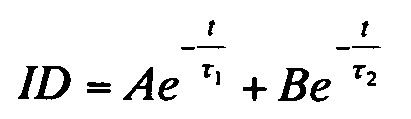
이 부분에서 설명되는 광응답 결함 평가법에서는, 60초의 암상태 후에, 600초 동안 광 조사를 행하고, 그 후 광 조사를 정지하고 3000초 동안 광전류의 완화를 측정하였다. 조사 광의 파장 및 강도는 각각 400nm 및 3.5mW/cm2이고, 샘플 N 및 샘플 O 각각의 게이트 전극 및 소스 전극을 0V로 고정하고, 드레인 전극에는 0.1V의 저전압을 인가하여 광전류의 값을 측정하였다. 샘플 N 및 샘플 O 각각의 채널 길이 L과 채널 폭 W는, 각각 30μm 및 10000μm라는 점에 주목한다.In the photoresponse defect evaluation method described in this section, after a dark state of 60 seconds, light irradiation was performed for 600 seconds, after which light irradiation was stopped and relaxation of the photocurrent was measured for 3000 seconds. The wavelength and intensity of the irradiated light were 400 nm and 3.5 mW / cm 2 , respectively, and the gate electrode and the source electrode of Sample N and Sample O were fixed at 0 V, and a low voltage of 0.1 V was applied to the drain electrode to measure the value of the photocurrent. . Note that the channel length L and the channel width W of each of the sample N and the sample O are 30 μm and 10000 μm, respectively.
도 26의 (A) 및 도 26의 (B)는 샘플 N 및 샘플 O의 광응답 결함 평가법에서의 광전류의 변화량을 도시하는 그래프이다. 도 26의 (A) 및 도 26의 (B)에 도시하는 그래프에서, 종축은 광전류 ID를 나타내고, 횡축은 시간 t(sec)를 나타낸다. 도 26의 (A) 및 도 26의 (B)에 도시한 그래프를, 지수 함수의 선형 결합으로 나타낸 수학식으로 피팅하면, 이하의 수학식이 된다.26A and 26B are graphs showing the amount of change in the photocurrent in the photoresponse defect evaluation method of Sample N and Sample O. In the graphs shown in Figs. 26A and 26B, the ordinate indicates the photocurrent ID, and the abscissa indicates the time t (sec). When the graphs shown in Figs. 26A and 26B are fitted with equations represented by linear combinations of exponential functions, the following equations are obtained.


도 26의 (A) 및 도 26의 (B)로부터, c축 배향의 결정 영역을 포함한 산화물 반도체막을 포함하는 샘플 N이 샘플 O보다 광전류의 최대값이 더 작고, 완화 시간 τ1과 완화 시간 τ2도 더 짧다는 것을 알았다. 샘플 N에 있어서, 광전류의 최대값 Imax는 6.2×10⁻¹¹A이며, 완화 시간 τ1은 0.3초, 완화 시간 τ2은 39초였다. 한편, 샘플 O에 있어서, 광전류의 최대값 Imax는 8.0×10⁻⁹A이며, 완화 시간 τ1은 3.9초, 완화 시간 τ2는 98초였다.26 (A) and 26 (B), the sample N including the oxide semiconductor film including the crystal region in the c-axis orientation has a smaller maximum value of the photocurrent than the sample O, the relaxation time τ 1 and the relaxation time τ I found 2 degrees shorter. In Sample N, the maximum value Imax of the photocurrent was 6.2 × 10 -11 A, the relaxation time τ 1 was 0.3 seconds, and the relaxation time τ 2 was 39 seconds. On the other hand, in Sample O, the maximum value Imax of the photocurrent was 8.0 × 10 −9 A, the relaxation time τ 1 was 3.9 seconds, and the relaxation time τ 2 was 98 seconds.
샘플 N 및 샘플 O 모두에서 적어도 2종류의 완화 시간을 갖는 지수 함수의 선형 결합에 의해, 광전류 ID의 완화의 피팅을 행할 수 있다는 것을 알았다. 이는 샘플 N 및 샘플 O 모두에서 광전류 ID의 완화가 2종류의 완화 과정을 갖는 것을 나타낸다. 이는 도 5의 (A) 및 도 5의 (B)에 도시한 2종류의 재결합 모델을 이용한 광전류의 완화 과정과 부합된다. 즉, 상기의 실시예에서 도 5의 (A) 및 도 5의 (B)의 밴드 다이어그램에서와 같이, 산화물 반도체의 밴드갭에서 트랩 준위가 존재하는 것으로 나타났다.It has been found that the relaxation of the photocurrent ID can be fitted by linear combination of exponential functions having at least two relaxation times in both sample N and sample O. This indicates that the relaxation of the photocurrent ID in both sample N and sample O has two types of relaxation processes. This is consistent with the relaxation process of the photocurrent using two types of recombination models shown in Figs. 5A and 5B. That is, in the above embodiment, as shown in the band diagrams of FIGS. 5 (A) and 5 (B), it was shown that a trap level exists in the band gap of the oxide semiconductor.
또한, c축 배향의 결정 영역을 포함한 산화물 반도체막을 포함하는 샘플 N이 샘플 O보다 완화 시간 τ1 및 완화 시간 τ2가 더 짧았다. 이는, 도 5의 (A) 및 도 5의 (B)의 재결합 모델에서의, 산소 결함에 기인하는 트랩 준위의 개수가 샘플 N이 샘플 O보다 더 작은 것을 나타낸다. 이는, 산화물 반도체막이 c축 배향의 결정 영역을 포함하므로, 샘플 N에서, 트랩 준위로서 기능할 수 있는 산화물 반도체막에서의 결함의 개수가 감소되었기 때문이다.Moreover, the relaxation time τ 1 and the relaxation time τ 2 of the sample N including the oxide semiconductor film including the crystal region in the c-axis orientation were shorter than that of the sample O. This indicates that in the recombination models of Figs. 5A and 5B, the number of trap levels due to oxygen defects is smaller than that of Sample O. This is because the number of defects in the oxide semiconductor film that can function as a trap level is reduced in Sample N because the oxide semiconductor film includes a crystal region in a c-axis orientation.
상기로부터, 산화물 반도체막에서 c축 배향의 결정 영역이 형성되는 것에 의해, 트랜지스터는 광 조사에 대하여 보다 안정된 구조를 갖는다. 이러한 산화물 반도체막을 트랜지스터에 이용함으로써 전기적 특성이 안정되고 신뢰성이 높은 트랜지스터를 제공할 수 있다.From the above, by forming a c-axis oriented crystal region in the oxide semiconductor film, the transistor has a more stable structure against light irradiation. By using such an oxide semiconductor film as a transistor, a transistor having stable electrical characteristics and high reliability can be provided.
<6. TDS 분석><6. TDS analysis>
이 부분에서, 상기의 실시예에 따라 산화물 반도체막을 형성하고, 산화물 반도체막을 TDS(Thermal Desorption Spectroscopy) 분석을 이용해서 평가하였다. 그 결과에 대해서 이하에서 설명한다.In this part, an oxide semiconductor film was formed according to the above example, and the oxide semiconductor film was evaluated using TDS (Thermal Desorption Spectroscopy) analysis. The results will be described below.
이 부분에서, 스퍼터링법에 의해 석영 기판 위에 산화물 반도체막을 형성하여, 성막 시의 기판 온도가 실온인 샘플 P1과, 성막 시의 기판 온도가 100℃인 샘플 P2와, 성막 시의 기판 온도가 200℃인 샘플 P3와, 성막 시의 기판 온도가 300℃인 샘플 P4와, 성막 시의 기판 온도가 400℃인 샘플 P5를 형성하였다. 본 명세서에서, 샘플 P1, 샘플 P2 및 샘플 P3 각각은, c축 배향의 결정 영역을 포함하지 않는 산화물 반도체막이며, 샘플 P4 및 샘플 P5 각각은, c축 배향의 결정 영역을 포함하는 산화물 반도체막이다. 산화물 반도체막을 형성하기 위한 타겟은, In2O3:Ga2O3:ZnO=1:1:2 [몰수비]의 조성비를 갖는다. 이외의 조건은 이하와 같았다: 형성 가스 흐름에 대해서, 아르곤 가스의 흐름은 30sccm이고, 산소 가스의 흐름은 15sccm이고, 압력은 0.4Pa이고, 기판과 타겟간 거리는 60mm이고, 무선 주파수(RF) 전력은 0.5kW이고, 막 두께는 50nm였다. TDS 분석시에 기판으로부터의 탈리 가스의 요인을 저감하기 위해서, 석영 기판에 미리 건조 분위기에서 850℃로 열처리를 하였다.In this part, an oxide semiconductor film is formed on the quartz substrate by sputtering, so that the sample P1 having the substrate temperature at the time of film formation, the sample P2 having the substrate temperature at 100 ° C during film formation, and the substrate temperature at the time of film formation are 200 ° C. A phosphorus sample P3, a sample P4 having a substrate temperature of 300 ° C during film formation, and a sample P5 having a substrate temperature of 400 ° C during film formation were formed. In the present specification, each of the sample P1, the sample P2, and the sample P3 is an oxide semiconductor film that does not include a c-axis oriented crystal region, and each of the samples P4 and sample P5 includes an c-axis oriented crystalline region. to be. The target for forming the oxide semiconductor film has a composition ratio of In 2 O 3 : Ga 2 O 3 : ZnO = 1: 1: 2 [molar ratio]. Other conditions were as follows: for the forming gas flow, the flow of argon gas was 30 sccm, the flow of oxygen gas was 15 sccm, the pressure was 0.4 Pa, the distance between the substrate and the target was 60 mm, and radio frequency (RF) power Was 0.5 kW, and the film thickness was 50 nm. In order to reduce the factors of the desorption gas from the substrate during TDS analysis, the quartz substrate was previously heat-treated at 850 ° C in a dry atmosphere.
TDS 분석은, 진공 용기 내의 샘플을 할로겐 램프를 이용해서 가열하고, 샘플의 온도가 증가되는 경우에 샘플 전체로부터 발생하는 가스 성분을 4중극 질량 분석계(QMS: Quardrupole Mass Spectrometer)에 의해 검출하는 분석 방법이라는 점에 주목한다. 검출되는 가스 성분은 M/z(질량/전하)의 값에 의해 서로 구별되어, 질량 스펙트럼의 형태로 검출된다.TDS analysis is a method of heating a sample in a vacuum container using a halogen lamp and detecting a gas component generated from the entire sample when the temperature of the sample is increased by a quadrupole mass spectrometer (QMS) Note that it is. The gas components to be detected are distinguished from each other by the value of M / z (mass / charge), and are detected in the form of a mass spectrum.
본 예에서, TDS 분석은 ESCO 주식회사 제조의 WA1000S를 이용해서 행하였다. 이하의 측정 조건 하에서 H2O에 상당하는 M/z=18의 질량 스펙트럼을 검출하였다: SEM 전압은 1500V이고, 기판 표면 온도는 실온 내지 400℃이고, 진공도는 1.5×10⁻⁷Pa 이하이고, Dwell Time은 0.2(sec/U)이고, 승온 속도는 30(℃/min)이었다.In this example, TDS analysis was performed using WA1000S manufactured by ESCO Corporation. A mass spectrum of M / z = 18 corresponding to H 2 O was detected under the following measurement conditions: the SEM voltage was 1500 V, the substrate surface temperature was from room temperature to 400 ° C., and the vacuum degree was 1.5 × 10 −7 Pa or less, Dwell Time was 0.2 (sec / U), and the heating rate was 30 (° C / min).
샘플 P1 내지 샘플 P5의 TDS 분석 결과를 도 27에 도시한다. 도 27에 도시한 그래프에서, 종축은 탈리되는 물 분자량(M/z=18)[molecules/cm3](counts)을 나타내고, 횡축은 기판 온도(℃)를 나타낸다. 본 명세서에서, 탈리된 물 분자량은, M/z=18인 질량 스펙트럼의 300℃ 근방의 온도에서의 적분값을 계산하여 얻어지며, 즉, 산화물 반도체막으로부터 탈리되는 물 분자량이다. M/z=18인 질량 스펙트럼에서, 온도가 100℃ 근방인 영역에서도 피크가 존재하지만, 이러한 피크는 산화물 반도체막의 표면에 흡착된 수분량을 나타내는 것으로 가정되어, 탈리된 물 분자량으로서 카운트하지 않는다.The results of TDS analysis of samples P1 to P5 are shown in FIG. 27. In the graph shown in Fig. 27, the vertical axis represents the water molecular weight (M / z = 18) [molecules / cm 3 ] (counts) to be removed, and the horizontal axis represents the substrate temperature (° C). In this specification, the desorbed water molecular weight is obtained by calculating the integral value at a temperature near 300 ° C of the mass spectrum with M / z = 18, that is, it is the water molecular weight desorbed from the oxide semiconductor film. In the mass spectrum of M / z = 18, peaks exist even in the region where the temperature is around 100 ° C, but these peaks are assumed to represent the amount of moisture adsorbed on the surface of the oxide semiconductor film, and are not counted as the molecular weight of the desorbed water.
도 27의 그래프는 성막 시의 기판 온도가 증가됨에 따라, 각 샘플로부터 탈리되는 물 분자량이 감소되는 것을 도시한다. 따라서, 성막 시의 기판 온도를 증가시킴으로써, 즉, 산화물 반도체막에 c축 배향의 결정 영역을 형성함으로써, 산화물 반도체막에 포함되는, H2O(물) 분자로 대표되는 H(수소 원자)를 포함하는 분자나 이온을 저감할 수 있다.The graph of FIG. 27 shows that as the substrate temperature during film deposition increases, the molecular weight of water desorbed from each sample decreases. Therefore, by increasing the substrate temperature during film formation, that is, by forming a c-axis oriented crystal region in the oxide semiconductor film, H (hydrogen atom) represented by H 2 O (water) molecules contained in the oxide semiconductor film is obtained. It is possible to reduce the molecules and ions included.
상술한 바와 같이, c축 배향의 결정 영역을 포함하는 산화물 반도체막을 형성함으로써, 산화물 반도체막에서 캐리어의 공급원일 수 있는, H2O(물) 분자로 대표되는 H(수소 원자)를 포함하는 분자나 이온 등의 불순물을 저감할 수 있다. 따라서, 산화물 반도체막의 전기 전도도가 변화되는 것을 방지하여, 산화물 반도체막을 포함한 트랜지스터의 신뢰성을 향상시킬 수 있다.As described above, by forming an oxide semiconductor film containing a crystal region in c-axis orientation, a molecule comprising H (hydrogen atom), represented by H 2 O (water) molecules, which may be a source of carriers in the oxide semiconductor film Impurities such as ions and ions can be reduced. Therefore, it is possible to prevent the electrical conductivity of the oxide semiconductor film from being changed, and to improve the reliability of the transistor including the oxide semiconductor film.
<7. 2차 이온 질량 분석><7. Secondary ion mass spectrometry>
이 부분에서는, 상기의 실시예에 따라 산화물 반도체막을 형성하고, 산화물 반도체막을 2차 이온 질량 분석(SIMS: Secondary Ion Mass Spectrometry)을 이용해서 평가하였다. 그 결과에 대해서 이하에서 설명한다.In this part, an oxide semiconductor film was formed according to the above example, and the oxide semiconductor film was evaluated using secondary ion mass spectrometry (SIMS). The results will be described below.
이 부분에서, 스퍼터링법을 이용해서 석영 기판 위에 산화물 반도체막을 형성하여, 성막 시의 기판 온도가 실온인 샘플 Q1 내지 샘플 Q7과, 성막 시의 기판 온도가 400℃인 샘플 R1 내지 샘플 R7을 형성하였다. 본 명세서에서, 샘플 Q1 내지 샘플 Q7 각각은, c축 배향의 결정 영역을 포함하지 않는 산화물 반도체막이며, 샘플 R1 내지 샘플 R7 각각은, c축 배향의 결정 영역을 포함하는 산화물 반도체막이다. 산화물 반도체막을 형성하기 위한 타겟은, In2O3:Ga2O3:ZnO=1:1:2 [몰수비]의 조성비를 갖는다. 이외의 조건은 이하와 같았다: 성막 가스 흐름에 대해서, 아르곤 가스의 흐름은 30sccm이고, 산소 가스의 흐름은 15sccm이고, 압력은 0.4Pa이고, 기판과 타겟간 거리는 60mm이고, 무선 주파수(RF) 전력은 0.5kW이고, 막 두께는 300nm였다. 석영 기판에, 미리 질소 분위기에서 850℃로 1시간 동안 열처리를 하였다.In this part, an oxide semiconductor film was formed on the quartz substrate using a sputtering method to form samples Q1 to sample Q7 having a substrate temperature at room temperature during film formation and samples R1 to sample R7 having a substrate temperature at 400 ° C during film formation. . In this specification, each of the samples Q1 to Q7 is an oxide semiconductor film that does not contain a crystal region in the c-axis orientation, and each of the samples R1 to sample R7 is an oxide semiconductor film that includes crystal regions in the c-axis orientation. The target for forming the oxide semiconductor film has a composition ratio of In 2 O 3 : Ga 2 O 3 : ZnO = 1: 1: 2 [molar ratio]. Other conditions were as follows: For the deposition gas flow, the flow of argon gas was 30 sccm, the flow of oxygen gas was 15 sccm, the pressure was 0.4 Pa, the distance between the substrate and the target was 60 mm, and radio frequency (RF) power Was 0.5 kW, and the film thickness was 300 nm. The quartz substrate was previously heat-treated at 850 ° C. for 1 hour in a nitrogen atmosphere.
샘플 Q2 내지 샘플 Q7, 샘플 R2 내지 샘플 R7 각각에 있어서, 산화물 반도체막을 형성한 후에, 산화물 반도체막이 형성된 석영 기판에 가열 처리를 행하였다. 가열 처리는 질소 분위기에서 미리 정해진(predetermined) 온도까지 온도를 증가시키고, 질소 분위기로부터 산소 분위기로 분위기를 전환하여 미리 정해진 온도를 1시간 동안 유지하고, 그 후 그 온도를 산소 분위기에서 감소시키는 방식으로 행하였다. 미리 정해진 온도는, 샘플 Q2 및 샘플 R2에서는 200℃이고, 샘플 Q3 및 샘플 R3에서는 250℃이고, 샘플 Q4 및 샘플 R4에서는 350℃이고, 샘플 Q5 및 샘플 R5에서는 450℃이고, 샘플 Q6 및 샘플 R6에서는 550℃이고, 샘플 Q7 및 샘플 R7에서는 650℃였다. 이러한 방식으로, 산화물 반도체막을 석영 기판 위에 각각 형성한 샘플 Q1 내지 샘플 Q7, 샘플 R1 내지 샘플 R7를 제조하였다.In each of Samples Q2 to Sample Q7 and Samples R2 to Sample R7, after forming the oxide semiconductor film, a heat treatment was performed on the quartz substrate on which the oxide semiconductor film was formed. The heat treatment is performed by increasing the temperature from a nitrogen atmosphere to a predetermined temperature, switching the atmosphere from the nitrogen atmosphere to the oxygen atmosphere, maintaining the predetermined temperature for 1 hour, and then reducing the temperature in the oxygen atmosphere. Was done. The predetermined temperature is 200 ° C in Sample Q2 and Sample R2, 250 ° C in Sample Q3 and Sample R3, 350 ° C in Sample Q4 and Sample R4, 450 ° C in Sample Q5 and Sample R5, Sample Q6 and Sample R6 It was 550 ° C in, and it was 650 ° C in Sample Q7 and Sample R7. In this way, samples Q1 to Q7 and samples R1 to R7, respectively, of which oxide semiconductor films were formed on a quartz substrate were prepared.
이 부분에서, 샘플 Q1 내지 샘플 Q7, 샘플 R1 내지 샘플 R7 각각에 SIMS 분석을 행하였다. 샘플 Q1 내지 샘플 Q7의 SIMS 분석 결과를 도 28의 (A)에 도시하고, 샘플 R1 내지 샘플 R7의 SIMS 분석 결과를 도 28의 (B)에 도시한다. 도 28의 (A) 및 도 28의 (B)에 도시한 그래프에서, 종축은 수소(H)의 농도(atoms/cm3)를 나타내고, 횡축은 산화물 반도체막 표면으로부터의 산화물 반도체막의 깊이(nm) 및 석영 기판의 깊이(nm)를 나타낸다.In this section, SIMS analysis was performed on samples Q1 to Q7 and samples R1 to R7, respectively. The results of SIMS analysis of samples Q1 to Q7 are shown in Fig. 28A, and the results of SIMS analysis of samples R1 to R7 are shown in Fig. 28B. In the graphs shown in FIGS. 28A and 28B, the vertical axis represents the concentration of hydrogen (H) (atoms / cm 3 ), and the horizontal axis represents the depth (nm) of the oxide semiconductor film from the surface of the oxide semiconductor film. ) And the depth (nm) of the quartz substrate.
도 28의 (A) 및 도 28의 (B)의 그래프로부터, 샘플 Q1과 샘플 R1의 산화물 반도체막에서의 수소 농도는 실질적으로 동등하지만, 샘플 R2 내지 샘플 R7의 산화물 반도체막에서의 수소 농도는 각각 샘플 Q2 내지 샘플 Q7보다 더 낮은 것으로 보인다. 이는, 산화물 반도체막 형성 시의 기판 온도가 높을수록, 나중에 행해진 가열 처리에서 산화물 반도체막에 수소의 혼입이 더 적게 일어나는 경향을 나타낸다. 특히, 샘플 Q3 내지 샘플 Q5의 그래프는, 가열 처리시의 온도를 증가시킴에 따라, 산화물 반도체막의 표면측으로부터 수소가 혼입되고, 수소 농도가 높은 층이 산화물 반도체막의 내부까지 넓어지고, 온도를 더 증가시키면 산화물 반도체막의 표면측으로부터 수소가 탈리되는 것을 도시한다. 이러한 방식으로, 산화물 반도체막이, c축 배향의 결정 영역을 포함하지 않을 경우, 가열 처리로 인한 수소의 혼입이나 탈리가 일어난다. 그러나, 산화물 반도체막에 c축 배향의 결정 영역을 각각 포함하는 샘플 R2 내지 샘플 R7에서는 이러한 현상은 관찰되지 않는다.From the graphs of FIGS. 28A and 28B, the hydrogen concentrations in the oxide semiconductor films of Sample Q1 and Sample R1 are substantially equal, but the hydrogen concentrations in the oxide semiconductor films of Samples R2 to R7 are It appears to be lower than Sample Q2 to Sample Q7 respectively. This indicates that the higher the substrate temperature at the time of forming the oxide semiconductor film, the less the incorporation of hydrogen into the oxide semiconductor film in the heat treatment performed later. In particular, in the graphs of the samples Q3 to Q5, as the temperature during heat treatment was increased, hydrogen was mixed from the surface side of the oxide semiconductor film, and a layer having a high hydrogen concentration widened to the inside of the oxide semiconductor film, further increasing the temperature. The increase shows that hydrogen is released from the surface side of the oxide semiconductor film. In this way, when the oxide semiconductor film does not include a c-axis oriented crystal region, hydrogen incorporation or desorption due to heat treatment occurs. However, this phenomenon is not observed in Samples R2 to R7, which each contain a crystal region of c-axis orientation in the oxide semiconductor film.
이는, 산화물 반도체 형성 시에 기판 온도를 증가시켜, 산화물 반도체막에 c축 배향의 결정 영역을 형성함으로써, 수소가 결합하기 쉬운 댕글링 본드 등이 산화물 반도체막에서 저감되기 때문이라고 생각할 수 있다.It can be considered that this is because the dangling bond, which is easily bonded to hydrogen, is reduced in the oxide semiconductor film by increasing the substrate temperature during the formation of the oxide semiconductor and forming a c-axis oriented crystal region in the oxide semiconductor film.
따라서, 산화물 반도체 형성 시에 기판 온도를 증가시켜서, 산화물 반도체막에 c축 배향의 결정 영역을 형성함으로써, 산화물 반도체막에서 캐리어의 공급원이 될 수 있는 수소가 가열 처리에 의해 증가하는 것을 방지할 수 있다. 따라서, 산화물 반도체막의 전기 전도도가 변화되는 것을 방지하여, 산화물 반도체막을 포함한 트랜지스터의 신뢰성을 향상시킬 수 있다.Therefore, by increasing the substrate temperature during the formation of the oxide semiconductor, by forming a c-axis oriented crystal region in the oxide semiconductor film, it is possible to prevent the hydrogen that can be a source of carriers in the oxide semiconductor film from being increased by heat treatment. have. Therefore, it is possible to prevent the electrical conductivity of the oxide semiconductor film from being changed, and to improve the reliability of the transistor including the oxide semiconductor film.
본원은 2010년 12월 3일에 일본 특허청에 출원된 일본 특허 출원 번호 제2010-270557호에 기초하며, 그 전체 내용은 본원에 참조로서 원용된다.This application is based on Japanese Patent Application No. 2010-270557 filed with the Japan Patent Office on December 3, 2010, the entire contents of which are incorporated herein by reference.
11: 사이트
12: In 원자
13: Ga 원자
14: Zn 원자
15: O 원자
31: 처리실
33: 배기 수단
35: 가스 공급 수단
37: 전원 장치
40: 기판 지지체
41: 타겟
43: 이온
45: 원자
47: 원자
51: 기판
53: 하지 절연막
55: 산화물 반도체막
56: 산화물 반도체막
59: 산화물 반도체막
63: 게이트 절연막
65: 게이트 전극
69: 절연막
120: 트랜지스터
130: 트랜지스터
140: 트랜지스터
150: 트랜지스터
160: 트랜지스터
170: 트랜지스터
180: 트랜지스터
351: 기판
353: 하지 절연막
359: 산화물 반도체막
363: 게이트 절연막
365: 게이트 전극
369: 절연막
371: 금속 산화물막
373: 금속 산화물막
55a: 시드 결정
55b: 산화물 반도체막
56a: 시드 결정
56b: 산화물 반도체막
61a: 소스 전극
61b: 드레인 전극
361a: 소스 전극
361b: 드레인 전극
500: 기판
501: 화소부
502: 주사선 구동 회로
503: 주사선 구동 회로
504: 신호선 구동 회로
510: 용량 배선
512: 게이트 배선
513: 게이트 배선
514: 드레인 전극층
516: 트랜지스터
517: 트랜지스터
518: 액정 소자
519: 액정 소자
520: 화소
521: 스위칭 트랜지스터
522: 구동 트랜지스터
523: 용량 소자
524: 발광 소자
525: 신호선
526: 주사선
527: 전원선
528: 공통 전극
1001: 본체
1002: 하우징
1004: 키보드 버튼
1021: 본체
1022: 고정부
1023: 표시부
1024: 조작 버튼
1025: 외부 메모리 슬롯
1030: 하우징
1031: 하우징
1032: 표시 패널
1033: 스피커
1034: 마이크
1035: 조작 키
1036: 포인팅 디바이스
1037: 카메라 렌즈
1038: 외부 접속 단자
1040: 태양 전지
1041: 외부 메모리 슬롯
1050: 텔레비전 장치
1051: 하우징
1052: 기억 매체 녹화 재생부
1053: 표시부
1054: 외부 접속 단자
1055: 스탠드
1056: 외부 메모리
1003a: 표시부
1003b: 표시부11: site
12: In atom
13: Ga atom
14: Zn atom
15: O atom
31: processing room
33: exhaust means
35: gas supply means
37: power supply
40: substrate support
41: target
43: ion
45: Atom
47: Atom
51: substrate
53: underlying insulating film
55: oxide semiconductor film
56: oxide semiconductor film
59: oxide semiconductor film
63: gate insulating film
65: gate electrode
69: insulating film
120: transistor
130: transistor
140: transistor
150: transistor
160: transistor
170: transistor
180: transistor
351: substrate
353: underlying insulating film
359: oxide semiconductor film
363: gate insulating film
365: gate electrode
369: insulating film
371: metal oxide film
373: metal oxide film
55a: seed crystal
55b: oxide semiconductor film
56a: Seed crystal
56b: oxide semiconductor film
61a: source electrode
61b: drain electrode
361a: source electrode
361b: drain electrode
500: substrate
501: pixel portion
502: scan line driving circuit
503: scan line driving circuit
504: signal line driving circuit
510: capacitive wiring
512: gate wiring
513: gate wiring
514: drain electrode layer
516: transistor
517: transistor
518: liquid crystal element
519: liquid crystal element
520: pixels
521: switching transistor
522: driving transistor
523: capacitive element
524: light emitting element
525: signal line
526: scan line
527: power line
528: common electrode
1001: main body
1002: housing
1004: keyboard button
1021: main body
1022: fixing part
1023: display
1024: Operation button
1025: external memory slot
1030: housing
1031: housing
1032: display panel
1033: speaker
1034: microphone
1035: operation keys
1036: pointing device
1037: camera lens
1038: external connection terminal
1040: solar cell
1041: external memory slot
1050: television device
1051: housing
1052: recording medium recording and playback unit
1053: display
1054: external connection terminal
1055: stand
1056: external memory
1003a: display unit
1003b: display unit
Claims (10)
상기 채널 영역은 실질적으로 c축 배향된 영역을 포함하고,
상기 산화물 반도체막은 인듐, 갈륨, 및 아연을 포함하는, 트랜지스터.A transistor comprising an oxide semiconductor film including a channel region,
The channel region comprises a region substantially c-axis oriented,
The oxide semiconductor film includes indium, gallium, and zinc, a transistor.
상기 채널 영역은 실질적으로 c축 배향된 영역을 포함하고,
상기 실질적으로 c축 배향된 영역에서 결정의 a-b면은 상기 채널 영역에서 캐리어 흐름 방향에 실질적으로 평행하고,
상기 산화물 반도체막은 인듐, 갈륨, 및 아연을 포함하는, 트랜지스터.A transistor comprising an oxide semiconductor film including a channel region,
The channel region comprises a region substantially c-axis oriented,
The ab plane of the crystal in the substantially c-axis oriented region is substantially parallel to the carrier flow direction in the channel region,
The oxide semiconductor film includes indium, gallium, and zinc, a transistor.
산화물 반도체막;
소스 전극; 및
드레인 전극
을 포함하고,
상기 산화물 반도체막은 채널 영역과, 상기 소스 전극 및 상기 드레인 전극 중 하나와 접하는 영역을 포함하고,
상기 채널 영역 및 상기 영역 각각은 실질적으로 c축 배향된 영역을 포함하고,
상기 산화물 반도체막은 인듐, 갈륨, 및 아연을 포함하는, 트랜지스터.As a transistor,
Oxide semiconductor film;
Source electrode; And
Drain electrode
Including,
The oxide semiconductor film includes a channel region, and a region in contact with one of the source electrode and the drain electrode,
Each of the channel region and the region includes a region substantially c-axis oriented,
The oxide semiconductor film includes indium, gallium, and zinc, a transistor.
상기 산화물 반도체막은 제1 영역, 제2 영역, 및 상기 제1 영역과 상기 제2 영역 사이의 채널 영역을 포함하고,
상기 채널 영역, 상기 제1 영역, 및 상기 제2 영역 각각은 실질적으로 c축 배향된 영역을 포함하고,
상기 산화물 반도체막은 인듐, 갈륨, 및 아연을 포함하는, 트랜지스터.A transistor comprising an oxide semiconductor film,
The oxide semiconductor film includes a first region, a second region, and a channel region between the first region and the second region,
Each of the channel region, the first region, and the second region includes a region substantially c-axis oriented,
The oxide semiconductor film includes indium, gallium, and zinc, a transistor.
상기 채널 영역은 실질적으로 c축 배향된 영역을 포함하고,
상기 실질적으로 c축 배향된 영역에서 결정의 a-b면은 상기 산화물 반도체막의 표면에 실질적으로 평행하고,
상기 산화물 반도체막은 인듐, 갈륨, 및 아연을 포함하는, 트랜지스터.A transistor comprising an oxide semiconductor film including a channel region,
The channel region comprises a region substantially c-axis oriented,
The ab surface of the crystal in the substantially c-axis oriented region is substantially parallel to the surface of the oxide semiconductor film,
The oxide semiconductor film includes indium, gallium, and zinc, a transistor.
상기 채널 영역은 각각 c축이 실질적으로 배향된 복수의 영역을 포함하고,
상기 복수의 영역 각각에서의 a축 또는 b축 방향들은 서로 상이하고,
상기 산화물 반도체막은 인듐, 갈륨, 및 아연을 포함하는, 트랜지스터.A transistor comprising an oxide semiconductor film including a channel region,
Each of the channel regions includes a plurality of regions in which the c-axis is substantially oriented,
The a-axis or b-axis directions in each of the plurality of regions are different from each other,
The oxide semiconductor film includes indium, gallium, and zinc, a transistor.
상기 채널 영역은 실질적으로 c축 배향된 영역을 포함하고,
결정립계(crystal boundary)는 상기 채널 영역의 단면 투과형 전자 현미경 상에서 관찰되지 않는, 트랜지스터.A transistor comprising an oxide semiconductor film including a channel region,
The channel region comprises a region substantially c-axis oriented,
A crystal boundary is not observed on the cross-section transmission electron microscope of the channel region, the transistor.
Priority Applications (1)
| Application Number | Priority Date | Filing Date | Title |
|---|---|---|---|
| KR1020227025885A KR102505248B1 (en) | 2010-12-03 | 2011-11-21 | Oxide semiconductor film and semiconductor device |
Applications Claiming Priority (3)
| Application Number | Priority Date | Filing Date | Title |
|---|---|---|---|
| JPJP-P-2010-270557 | 2010-12-03 | ||
| JP2010270557 | 2010-12-03 | ||
| PCT/JP2011/077292 WO2012073844A1 (en) | 2010-12-03 | 2011-11-21 | Oxide semiconductor film and semiconductor device |
Related Parent Applications (1)
| Application Number | Title | Priority Date | Filing Date |
|---|---|---|---|
| KR1020197018131A Division KR102110496B1 (en) | 2010-12-03 | 2011-11-21 | Oxide semiconductor film and semiconductor device |
Related Child Applications (1)
| Application Number | Title | Priority Date | Filing Date |
|---|---|---|---|
| KR1020227025885A Division KR102505248B1 (en) | 2010-12-03 | 2011-11-21 | Oxide semiconductor film and semiconductor device |
Publications (1)
| Publication Number | Publication Date |
|---|---|
| KR20200052993A true KR20200052993A (en) | 2020-05-15 |
Family
ID=46161371
Family Applications (9)
| Application Number | Title | Priority Date | Filing Date |
|---|---|---|---|
| KR1020137018239A KR101457833B1 (en) | 2010-12-03 | 2011-11-21 | Semiconductor device |
| KR1020197018131A KR102110496B1 (en) | 2010-12-03 | 2011-11-21 | Oxide semiconductor film and semiconductor device |
| KR1020237006773A KR102637010B1 (en) | 2010-12-03 | 2011-11-21 | Oxide semiconductor film and semiconductor device |
| KR1020227025885A KR102505248B1 (en) | 2010-12-03 | 2011-11-21 | Oxide semiconductor film and semiconductor device |
| KR1020247004791A KR20240025046A (en) | 2010-12-03 | 2011-11-21 | Oxide semiconductor film and semiconductor device |
| KR1020137015848A KR101995082B1 (en) | 2010-12-03 | 2011-11-21 | Oxide semiconductor film and semiconductor device |
| KR1020207013143A KR20200052993A (en) | 2010-12-03 | 2011-11-21 | Oxide semiconductor film and semiconductor device |
| KR1020147019793A KR101749387B1 (en) | 2010-12-03 | 2011-11-21 | Semiconductor device |
| KR1020157022686A KR101763052B1 (en) | 2010-12-03 | 2011-11-21 | Semiconductor device |
Family Applications Before (6)
| Application Number | Title | Priority Date | Filing Date |
|---|---|---|---|
| KR1020137018239A KR101457833B1 (en) | 2010-12-03 | 2011-11-21 | Semiconductor device |
| KR1020197018131A KR102110496B1 (en) | 2010-12-03 | 2011-11-21 | Oxide semiconductor film and semiconductor device |
| KR1020237006773A KR102637010B1 (en) | 2010-12-03 | 2011-11-21 | Oxide semiconductor film and semiconductor device |
| KR1020227025885A KR102505248B1 (en) | 2010-12-03 | 2011-11-21 | Oxide semiconductor film and semiconductor device |
| KR1020247004791A KR20240025046A (en) | 2010-12-03 | 2011-11-21 | Oxide semiconductor film and semiconductor device |
| KR1020137015848A KR101995082B1 (en) | 2010-12-03 | 2011-11-21 | Oxide semiconductor film and semiconductor device |
Family Applications After (2)
| Application Number | Title | Priority Date | Filing Date |
|---|---|---|---|
| KR1020147019793A KR101749387B1 (en) | 2010-12-03 | 2011-11-21 | Semiconductor device |
| KR1020157022686A KR101763052B1 (en) | 2010-12-03 | 2011-11-21 | Semiconductor device |
Country Status (7)
| Country | Link |
|---|---|
| US (8) | US8669556B2 (en) |
| JP (13) | JP2012134475A (en) |
| KR (9) | KR101457833B1 (en) |
| CN (3) | CN103500712B (en) |
| DE (1) | DE112011104002B4 (en) |
| TW (9) | TWI692109B (en) |
| WO (1) | WO2012073844A1 (en) |
Families Citing this family (358)
| Publication number | Priority date | Publication date | Assignee | Title |
|---|---|---|---|---|
| KR101457833B1 (en) * | 2010-12-03 | 2014-11-05 | 가부시키가이샤 한도오따이 에네루기 켄큐쇼 | Semiconductor device |
| KR101895325B1 (en) | 2010-12-17 | 2018-09-05 | 가부시키가이샤 한도오따이 에네루기 켄큐쇼 | Oxde material and semiconductor device |
| US9331206B2 (en) | 2011-04-22 | 2016-05-03 | Semiconductor Energy Laboratory Co., Ltd. | Oxide material and semiconductor device |
| US8969154B2 (en) * | 2011-08-23 | 2015-03-03 | Micron Technology, Inc. | Methods for fabricating semiconductor device structures and arrays of vertical transistor devices |
| WO2013047629A1 (en) | 2011-09-29 | 2013-04-04 | Semiconductor Energy Laboratory Co., Ltd. | Semiconductor device |
| CN104025301B (en) | 2011-10-14 | 2017-01-18 | 株式会社半导体能源研究所 | Semiconductor device |
| KR20130040706A (en) | 2011-10-14 | 2013-04-24 | 가부시키가이샤 한도오따이 에네루기 켄큐쇼 | Semiconductor device and method of manufacturing semiconductor device |
| JP5899237B2 (en) | 2011-11-18 | 2016-04-06 | シャープ株式会社 | Semiconductor device, display device, and method of manufacturing semiconductor device |
| JP2013149953A (en) | 2011-12-20 | 2013-08-01 | Semiconductor Energy Lab Co Ltd | Semiconductor device and method for manufacturing semiconductor device |
| US9035302B2 (en) | 2011-12-28 | 2015-05-19 | Sharp Kabushiki Kaisha | Active matrix including stressed capacitor insulation |
| KR102103913B1 (en) * | 2012-01-10 | 2020-04-23 | 가부시키가이샤 한도오따이 에네루기 켄큐쇼 | Semiconductor device and method for manufacturing semiconductor device |
| CN104040724B (en) | 2012-01-11 | 2016-11-09 | 夏普株式会社 | The manufacture method of semiconductor device, display device and semiconductor device |
| WO2013105537A1 (en) | 2012-01-11 | 2013-07-18 | シャープ株式会社 | Semiconductor device, display device, and semiconductor device manufacturing method |
| US9419146B2 (en) | 2012-01-26 | 2016-08-16 | Semiconductor Energy Laboratory Co., Ltd. | Semiconductor device and method for manufacturing the same |
| MY183237A (en) | 2012-01-31 | 2021-02-18 | Sharp Kk | Semiconductor device and method for producing same |
| CN104094386B (en) | 2012-01-31 | 2017-06-23 | 夏普株式会社 | Semiconductor device and its manufacture method |
| CN104081507B (en) | 2012-01-31 | 2017-03-22 | 夏普株式会社 | Semiconductor device and method for producing same |
| US9735280B2 (en) * | 2012-03-02 | 2017-08-15 | Semiconductor Energy Laboratory Co., Ltd. | Semiconductor device, method for manufacturing semiconductor device, and method for forming oxide film |
| CN104220926B (en) | 2012-03-27 | 2016-10-05 | 夏普株式会社 | Semiconductor device, the manufacture method of semiconductor device and display device |
| US9341904B2 (en) | 2012-04-04 | 2016-05-17 | Sharp Kabushiki Kaisha | Liquid-crystal display apparatus with large viewing angle and high optical transmittance |
| CN104205341B (en) | 2012-04-04 | 2017-04-05 | 夏普株式会社 | Semiconductor device and its manufacture method |
| US8901556B2 (en) | 2012-04-06 | 2014-12-02 | Semiconductor Energy Laboratory Co., Ltd. | Insulating film, method for manufacturing semiconductor device, and semiconductor device |
| CN104205310B (en) | 2012-04-06 | 2017-03-01 | 夏普株式会社 | Semiconductor device and its manufacture method |
| JP6128906B2 (en) | 2012-04-13 | 2017-05-17 | 株式会社半導体エネルギー研究所 | Semiconductor device |
| JP6143423B2 (en) * | 2012-04-16 | 2017-06-07 | 株式会社半導体エネルギー研究所 | Manufacturing method of semiconductor device |
| US9726953B2 (en) | 2012-04-18 | 2017-08-08 | Sharp Kabushiki Kaisha | Active matrix substrate and liquid-crystal display device |
| US20130320335A1 (en) * | 2012-06-01 | 2013-12-05 | Semiconductor Energy Laboratory Co., Ltd. | Semiconductor device and method for manufacturing the same |
| US9305939B2 (en) * | 2012-06-08 | 2016-04-05 | Sharp Kabushiki Kaisha | Semiconductor device with oxide layer as transparent electrode |
| KR20140011945A (en) * | 2012-07-19 | 2014-01-29 | 가부시키가이샤 한도오따이 에네루기 켄큐쇼 | Sputtering target, method for using the same, and method for forming oxide film |
| JP6022838B2 (en) * | 2012-07-20 | 2016-11-09 | 株式会社半導体エネルギー研究所 | Evaluation method of oxide semiconductor film |
| WO2014013959A1 (en) | 2012-07-20 | 2014-01-23 | Semiconductor Energy Laboratory Co., Ltd. | Semiconductor device and method for manufacturing semiconductor device |
| JP2014042004A (en) * | 2012-07-26 | 2014-03-06 | Semiconductor Energy Lab Co Ltd | Semiconductor device and manufacturing method of the same |
| JP6224931B2 (en) * | 2012-07-27 | 2017-11-01 | 株式会社半導体エネルギー研究所 | Semiconductor device |
| WO2014021249A1 (en) * | 2012-08-02 | 2014-02-06 | シャープ株式会社 | Semiconductor device and production method therefor |
| SG11201505225TA (en) | 2012-08-03 | 2015-08-28 | Semiconductor Energy Lab | Oxide semiconductor stacked film and semiconductor device |
| JP5654648B2 (en) * | 2012-08-10 | 2015-01-14 | 株式会社半導体エネルギー研究所 | Metal oxide film |
| KR20150043307A (en) * | 2012-08-10 | 2015-04-22 | 가부시키가이샤 한도오따이 에네루기 켄큐쇼 | Semiconductor device and method for fabricating the same |
| JP6220597B2 (en) * | 2012-08-10 | 2017-10-25 | 株式会社半導体エネルギー研究所 | Semiconductor device |
| US9245958B2 (en) * | 2012-08-10 | 2016-01-26 | Semiconductor Energy Laboratory Co., Ltd. | Semiconductor device and method for manufacturing the same |
| US9929276B2 (en) * | 2012-08-10 | 2018-03-27 | Semiconductor Energy Laboratory Co., Ltd. | Semiconductor device and method for manufacturing the same |
| JP6211843B2 (en) * | 2012-08-10 | 2017-10-11 | 株式会社半導体エネルギー研究所 | Semiconductor device |
| KR20140026257A (en) | 2012-08-23 | 2014-03-05 | 가부시키가이샤 한도오따이 에네루기 켄큐쇼 | Display device |
| WO2014042116A1 (en) | 2012-09-11 | 2014-03-20 | シャープ株式会社 | Semiconductor device and display device |
| WO2014042125A1 (en) * | 2012-09-12 | 2014-03-20 | シャープ株式会社 | Semiconductor device and method for manufacturing same |
| US9514693B2 (en) | 2012-09-13 | 2016-12-06 | Sharp Kabushiki Kaisha | Liquid crystal display device |
| MY175398A (en) | 2012-09-13 | 2020-06-24 | Sharp Kk | Liquid crystal display device |
| KR102211215B1 (en) * | 2012-09-14 | 2021-02-02 | 가부시키가이샤 한도오따이 에네루기 켄큐쇼 | Semiconductor device and method for fabricating the same |
| TWI709244B (en) | 2012-09-24 | 2020-11-01 | 日商半導體能源研究所股份有限公司 | Semiconductor device |
| JP6033045B2 (en) * | 2012-10-17 | 2016-11-30 | 株式会社半導体エネルギー研究所 | Semiconductor device |
| JP5951442B2 (en) * | 2012-10-17 | 2016-07-13 | 株式会社半導体エネルギー研究所 | Semiconductor device |
| US9166021B2 (en) * | 2012-10-17 | 2015-10-20 | Semiconductor Energy Laboratory Co., Ltd. | Semiconductor device and method for manufacturing the same |
| KR102227591B1 (en) | 2012-10-17 | 2021-03-15 | 가부시키가이샤 한도오따이 에네루기 켄큐쇼 | Semiconductor device |
| JP6246549B2 (en) * | 2012-10-17 | 2017-12-13 | 株式会社半導体エネルギー研究所 | Method for manufacturing semiconductor device |
| JP6204145B2 (en) | 2012-10-23 | 2017-09-27 | 株式会社半導体エネルギー研究所 | Semiconductor device |
| KR102279459B1 (en) * | 2012-10-24 | 2021-07-19 | 가부시키가이샤 한도오따이 에네루기 켄큐쇼 | Semiconductor device and method for manufacturing the same |
| WO2014065343A1 (en) * | 2012-10-24 | 2014-05-01 | Semiconductor Energy Laboratory Co., Ltd. | Semiconductor device |
| WO2014069260A1 (en) | 2012-10-29 | 2014-05-08 | シャープ株式会社 | Active-matrix substrate and liquid-crystal display device |
| WO2014073585A1 (en) | 2012-11-08 | 2014-05-15 | Semiconductor Energy Laboratory Co., Ltd. | Metal oxide film and method for forming metal oxide film |
| US9263531B2 (en) * | 2012-11-28 | 2016-02-16 | Semiconductor Energy Laboratory Co., Ltd. | Oxide semiconductor film, film formation method thereof, and semiconductor device |
| US9368521B2 (en) | 2012-11-30 | 2016-06-14 | Sharp Kabushiki Kaisha | TFT substrate |
| TWI624949B (en) | 2012-11-30 | 2018-05-21 | 半導體能源研究所股份有限公司 | Semiconductor device |
| CN108493253B (en) * | 2012-11-30 | 2023-04-25 | 株式会社半导体能源研究所 | Semiconductor device with a semiconductor device having a plurality of semiconductor chips |
| US9153649B2 (en) * | 2012-11-30 | 2015-10-06 | Semiconductor Energy Laboratory Co., Ltd. | Semiconductor device and method for evaluating semiconductor device |
| US9406810B2 (en) * | 2012-12-03 | 2016-08-02 | Semiconductor Energy Laboratory Co., Ltd. | Semiconductor device and manufacturing method thereof |
| KR102207028B1 (en) * | 2012-12-03 | 2021-01-22 | 가부시키가이샤 한도오따이 에네루기 켄큐쇼 | Semiconductor device |
| US9349593B2 (en) | 2012-12-03 | 2016-05-24 | Semiconductor Energy Laboratory Co., Ltd. | Method for manufacturing semiconductor device |
| KR20140072679A (en) * | 2012-12-05 | 2014-06-13 | 삼성디스플레이 주식회사 | Thin film transistor |
| KR102241249B1 (en) | 2012-12-25 | 2021-04-15 | 가부시키가이샤 한도오따이 에네루기 켄큐쇼 | Resistor, display device, and electronic device |
| DE112013006219T5 (en) | 2012-12-25 | 2015-09-24 | Semiconductor Energy Laboratory Co., Ltd. | Semiconductor device and its manufacturing method |
| KR20230023050A (en) | 2012-12-28 | 2023-02-16 | 가부시키가이샤 한도오따이 에네루기 켄큐쇼 | Semiconductor device |
| US9679925B2 (en) | 2013-01-10 | 2017-06-13 | Sharper Kabushiki Kaisha | Active matrix substrate, display device, defect modification method for display device, and method for manufacturing display device |
| US9651835B2 (en) | 2013-01-11 | 2017-05-16 | Sharp Kabushiki Kaisha | Display panel |
| US9391096B2 (en) * | 2013-01-18 | 2016-07-12 | Semiconductor Energy Laboratory Co., Ltd. | Semiconductor device and method for manufacturing the same |
| TWI614813B (en) | 2013-01-21 | 2018-02-11 | 半導體能源研究所股份有限公司 | Method for manufacturing semiconductor device |
| US8981374B2 (en) * | 2013-01-30 | 2015-03-17 | Semiconductor Energy Laboratory Co., Ltd. | Semiconductor device |
| US9190527B2 (en) * | 2013-02-13 | 2015-11-17 | Semiconductor Energy Laboratory Co., Ltd. | Semiconductor device and manufacturing method of semiconductor device |
| JP6329779B2 (en) * | 2013-02-25 | 2018-05-23 | 株式会社半導体エネルギー研究所 | Semiconductor device |
| JP6141777B2 (en) * | 2013-02-28 | 2017-06-07 | 株式会社半導体エネルギー研究所 | Method for manufacturing semiconductor device |
| JP6250883B2 (en) * | 2013-03-01 | 2017-12-20 | 株式会社半導体エネルギー研究所 | Semiconductor device |
| KR102153110B1 (en) * | 2013-03-06 | 2020-09-07 | 가부시키가이샤 한도오따이 에네루기 켄큐쇼 | Semiconductor film and semiconductor device |
| CN105027296B (en) | 2013-03-07 | 2018-11-06 | 夏普株式会社 | Semiconductor device and its manufacturing method |
| JP6298657B2 (en) * | 2013-03-07 | 2018-03-20 | 株式会社半導体エネルギー研究所 | Semiconductor device |
| JP6199581B2 (en) * | 2013-03-08 | 2017-09-20 | 株式会社半導体エネルギー研究所 | Metal oxide film and semiconductor device |
| TWI644433B (en) * | 2013-03-13 | 2018-12-11 | 半導體能源研究所股份有限公司 | Semiconductor device |
| US9577107B2 (en) * | 2013-03-19 | 2017-02-21 | Semiconductor Energy Laboratory Co., Ltd. | Oxide semiconductor film and method for forming oxide semiconductor film |
| US9153650B2 (en) | 2013-03-19 | 2015-10-06 | Semiconductor Energy Laboratory Co., Ltd. | Oxide semiconductor |
| US9368636B2 (en) * | 2013-04-01 | 2016-06-14 | Semiconductor Energy Laboratory Co., Ltd. | Method for manufacturing a semiconductor device comprising a plurality of oxide semiconductor layers |
| TWI620324B (en) * | 2013-04-12 | 2018-04-01 | 半導體能源研究所股份有限公司 | Semiconductor device |
| US10304859B2 (en) | 2013-04-12 | 2019-05-28 | Semiconductor Energy Laboratory Co., Ltd. | Semiconductor device having an oxide film on an oxide semiconductor film |
| US9685129B2 (en) | 2013-04-23 | 2017-06-20 | Sharp Kabushiki Kaisha | Liquid crystal display device |
| WO2014174905A1 (en) | 2013-04-23 | 2014-10-30 | シャープ株式会社 | Display device and drive current detection method for same |
| US9658491B2 (en) | 2013-04-24 | 2017-05-23 | Sharp Kabushiki Kaisha | Optical apparatus and display apparatus provided with same |
| US9583515B2 (en) | 2013-04-25 | 2017-02-28 | Sharp Kabushiki Kaisha | Semiconductor device including substrate which is used in display devices |
| CN105144276B (en) | 2013-04-25 | 2017-12-19 | 夏普株式会社 | Display device and its driving method |
| KR102222344B1 (en) * | 2013-05-02 | 2021-03-02 | 가부시키가이샤 한도오따이 에네루기 켄큐쇼 | Semiconductor device |
| WO2014185122A1 (en) | 2013-05-15 | 2014-11-20 | シャープ株式会社 | Liquid crystal display device |
| US9312392B2 (en) * | 2013-05-16 | 2016-04-12 | Semiconductor Energy Laboratory Co., Ltd. | Semiconductor device |
| DE102014208859B4 (en) * | 2013-05-20 | 2021-03-11 | Semiconductor Energy Laboratory Co., Ltd. | Semiconductor device |
| KR102537022B1 (en) * | 2013-05-20 | 2023-05-30 | 가부시키가이샤 한도오따이 에네루기 켄큐쇼 | Semiconductor device |
| WO2014188983A1 (en) | 2013-05-21 | 2014-11-27 | Semiconductor Energy Laboratory Co., Ltd. | Oxide semiconductor film and formation method thereof |
| WO2014188750A1 (en) | 2013-05-22 | 2014-11-27 | シャープ株式会社 | Display device and display control circuit |
| US9806198B2 (en) * | 2013-06-05 | 2017-10-31 | Semiconductor Energy Laboratory Co., Ltd. | Semiconductor device and method for manufacturing the same |
| JP6400336B2 (en) | 2013-06-05 | 2018-10-03 | 株式会社半導体エネルギー研究所 | Semiconductor device |
| WO2014199677A1 (en) * | 2013-06-10 | 2014-12-18 | シャープ株式会社 | Display device |
| TWI652822B (en) | 2013-06-19 | 2019-03-01 | 日商半導體能源研究所股份有限公司 | Oxide semiconductor film and formation method thereof |
| WO2014208458A1 (en) | 2013-06-27 | 2014-12-31 | シャープ株式会社 | Display device and drive method therefor |
| JP6138254B2 (en) | 2013-06-27 | 2017-05-31 | シャープ株式会社 | Display device and driving method thereof |
| US20150001533A1 (en) * | 2013-06-28 | 2015-01-01 | Semiconductor Energy Laboratory Co., Ltd. | Semiconductor device |
| JPWO2014208123A1 (en) | 2013-06-28 | 2017-02-23 | シャープ株式会社 | Unit shift register circuit, shift register circuit, method for controlling unit shift register circuit, and display device |
| JP6322503B2 (en) * | 2013-07-16 | 2018-05-09 | 株式会社半導体エネルギー研究所 | Semiconductor device |
| TWI608523B (en) * | 2013-07-19 | 2017-12-11 | 半導體能源研究所股份有限公司 | Oxide semiconductor film, method of manufacturing oxide semiconductor film, and semiconductor device |
| CN105408808B (en) | 2013-07-26 | 2018-09-14 | 夏普株式会社 | Liquid crystal display device |
| US9697769B2 (en) | 2013-07-30 | 2017-07-04 | Sharp Kabushiki Kaisha | Display device and drive method for same |
| US9496330B2 (en) | 2013-08-02 | 2016-11-15 | Semiconductor Energy Laboratory Co., Ltd. | Oxide semiconductor film and semiconductor device |
| US9583510B2 (en) | 2013-08-07 | 2017-02-28 | Sharp Kabushiki Kaisha | Semiconductor device, display device, and method for manufacturing semiconductor device |
| US9299855B2 (en) | 2013-08-09 | 2016-03-29 | Semiconductor Energy Laboratory Co., Ltd. | Semiconductor device having dual gate insulating layers |
| JP2015041388A (en) * | 2013-08-20 | 2015-03-02 | 株式会社半導体エネルギー研究所 | Storage device and semiconductor device |
| US9443987B2 (en) * | 2013-08-23 | 2016-09-13 | Semiconductor Energy Laboratory Co., Ltd. | Semiconductor device |
| CN105518773B (en) | 2013-09-05 | 2018-05-29 | 夏普株式会社 | Liquid crystal display device |
| US9716003B2 (en) * | 2013-09-13 | 2017-07-25 | Semiconductor Energy Laboratory Co., Ltd. | Method of manufacturing semiconductor device |
| TWI646690B (en) * | 2013-09-13 | 2019-01-01 | 半導體能源研究所股份有限公司 | Semiconductor device and manufacturing method thereof |
| US9397153B2 (en) * | 2013-09-23 | 2016-07-19 | Semiconductor Energy Laboratory Co., Ltd. | Semiconductor device |
| JP6383616B2 (en) * | 2013-09-25 | 2018-08-29 | 株式会社半導体エネルギー研究所 | Semiconductor device |
| CN103489828B (en) * | 2013-09-30 | 2015-07-01 | 深圳市华星光电技术有限公司 | Method for manufacturing thin film transistor array substrate |
| JP6101357B2 (en) | 2013-10-09 | 2017-03-22 | シャープ株式会社 | Semiconductor device and manufacturing method thereof |
| TW202203465A (en) | 2013-10-10 | 2022-01-16 | 日商半導體能源研究所股份有限公司 | Liquid crystal display device |
| CN105637637B (en) | 2013-10-11 | 2018-08-24 | 夏普株式会社 | Semiconductor device |
| US9502133B2 (en) | 2013-10-11 | 2016-11-22 | Sharp Kabushiki Kaisha | Semiconductor device |
| US9959801B2 (en) | 2013-10-21 | 2018-05-01 | Sharp Kabushiki Kaisha | Display device and method for driving same with light-emission enable signal switching unit |
| JP6196319B2 (en) | 2013-11-05 | 2017-09-13 | シャープ株式会社 | Display device and driving method thereof |
| CN105765720B (en) | 2013-11-18 | 2019-06-14 | 夏普株式会社 | Semiconductor device |
| US9859016B2 (en) * | 2013-11-25 | 2018-01-02 | Sharp Kabushiki Kaisha | Semiconductor device and method for writing thereto |
| US10269831B2 (en) | 2013-11-26 | 2019-04-23 | Sharp Kabushiki Kaisha | Semiconductor device including a plurality of thin-film transistors with one thin-film transistor including two gate electrodes |
| CN105793773B (en) * | 2013-12-02 | 2019-01-01 | 夏普株式会社 | Liquid crystal display panel and its active-matrix substrate used |
| JP6181203B2 (en) | 2013-12-10 | 2017-08-16 | シャープ株式会社 | Semiconductor device and manufacturing method thereof |
| TWI642186B (en) | 2013-12-18 | 2018-11-21 | 日商半導體能源研究所股份有限公司 | Semiconductor device |
| TWI666770B (en) * | 2013-12-19 | 2019-07-21 | 日商半導體能源研究所股份有限公司 | Semiconductor device |
| US9379192B2 (en) * | 2013-12-20 | 2016-06-28 | Semiconductor Energy Laboratory Co., Ltd. | Semiconductor device |
| US9842545B2 (en) | 2013-12-20 | 2017-12-12 | Sharp Kabushiki Kaisha | Display device and method for driving same |
| US9722049B2 (en) * | 2013-12-23 | 2017-08-01 | Intermolecular, Inc. | Methods for forming crystalline IGZO with a seed layer |
| WO2015097586A1 (en) * | 2013-12-25 | 2015-07-02 | Semiconductor Energy Laboratory Co., Ltd. | Semiconductor device |
| US9401432B2 (en) * | 2014-01-16 | 2016-07-26 | Semiconductor Energy Laboratory Co., Ltd. | Semiconductor device and electronic device |
| WO2015114476A1 (en) | 2014-01-28 | 2015-08-06 | Semiconductor Energy Laboratory Co., Ltd. | Semiconductor device |
| US9653487B2 (en) | 2014-02-05 | 2017-05-16 | Semiconductor Energy Laboratory Co., Ltd. | Semiconductor device, manufacturing method thereof, module, and electronic device |
| US10012883B2 (en) | 2014-02-10 | 2018-07-03 | Sharp Kabushiki Kaisha | Semiconductor device including a silicon nitride dielectric layer and method for producing same |
| CN105993077B (en) | 2014-02-14 | 2019-12-06 | 夏普株式会社 | active matrix substrate |
| KR102317297B1 (en) * | 2014-02-19 | 2021-10-26 | 가부시키가이샤 한도오따이 에네루기 켄큐쇼 | Oxide, semiconductor device, module, and electronic device |
| US9608008B2 (en) | 2014-02-21 | 2017-03-28 | Sharp Kabushiki Kaisha | Active matrix substrate and method for producing same |
| WO2015133469A1 (en) * | 2014-03-05 | 2015-09-11 | シャープ株式会社 | Lcd device |
| WO2015137337A1 (en) | 2014-03-11 | 2015-09-17 | シャープ株式会社 | Semiconductor device and method for manufacturing same |
| US10193101B2 (en) | 2014-03-26 | 2019-01-29 | Sharp Kabushiki Kaisha | Electronic device |
| WO2015151927A1 (en) | 2014-03-31 | 2015-10-08 | シャープ株式会社 | Display device and method for driving same |
| WO2015159800A1 (en) | 2014-04-16 | 2015-10-22 | シャープ株式会社 | Liquid crystal display panel and method for producing same |
| WO2015163288A1 (en) * | 2014-04-21 | 2015-10-29 | シャープ株式会社 | Light detection device |
| JP6227125B2 (en) * | 2014-04-25 | 2017-11-08 | シャープ株式会社 | Liquid crystal display |
| JP6537341B2 (en) * | 2014-05-07 | 2019-07-03 | 株式会社半導体エネルギー研究所 | Semiconductor device |
| CN103996717B (en) * | 2014-05-07 | 2015-08-26 | 京东方科技集团股份有限公司 | Thin-film transistor and preparation method thereof, display base plate and display unit |
| WO2015186602A1 (en) | 2014-06-03 | 2015-12-10 | シャープ株式会社 | Semiconductor device and method for manufacturing same |
| CN106663685A (en) * | 2014-06-06 | 2017-05-10 | 夏普株式会社 | Semiconductor device and method for manufacturing same |
| WO2015189731A1 (en) | 2014-06-13 | 2015-12-17 | Semiconductor Energy Laboratory Co., Ltd. | Semiconductor device and electronic device including the semiconductor device |
| US9792858B2 (en) | 2014-06-23 | 2017-10-17 | Sharp Kabushiki Kaisha | Display device and method for driving same |
| WO2015198957A1 (en) | 2014-06-25 | 2015-12-30 | シャープ株式会社 | Display device and method for driving same |
| CN106663404A (en) | 2014-07-15 | 2017-05-10 | 夏普株式会社 | Display device and driving method therefor |
| US10269316B2 (en) | 2014-08-26 | 2019-04-23 | Sharp Kabushiki Kaisha | Method for driving a display device including flicker check circuitry |
| WO2016035811A1 (en) | 2014-09-05 | 2016-03-10 | シャープ株式会社 | Liquid crystal display panel |
| CN107078165B (en) | 2014-09-10 | 2020-10-02 | 夏普株式会社 | Semiconductor device, liquid crystal display device, and method for manufacturing semiconductor device |
| US10074333B2 (en) | 2014-09-17 | 2018-09-11 | Sharp Kabushiki Kaisha | Display device and method for driving same |
| KR20160034200A (en) | 2014-09-19 | 2016-03-29 | 가부시키가이샤 한도오따이 에네루기 켄큐쇼 | Method for manufacturing semiconductor device |
| WO2016056452A1 (en) | 2014-10-08 | 2016-04-14 | シャープ株式会社 | Semiconductor device and method for manufacturing same |
| US9991393B2 (en) * | 2014-10-16 | 2018-06-05 | Semiconductor Energy Laboratory Co., Ltd. | Semiconductor device, module, and electronic device |
| TWI652362B (en) | 2014-10-28 | 2019-03-01 | 日商半導體能源研究所股份有限公司 | Oxide and manufacturing method thereof |
| TWI581317B (en) * | 2014-11-14 | 2017-05-01 | 群創光電股份有限公司 | Thin film transistor substrate and displaypanel having the thin film transistor substrate |
| CN105655344B (en) * | 2014-11-14 | 2019-02-05 | 群创光电股份有限公司 | Thin film transistor base plate and the display panel for having the thin film transistor base plate |
| CN107004718B (en) | 2014-11-28 | 2021-02-19 | 夏普株式会社 | Semiconductor device and method for manufacturing the same |
| US20170323907A1 (en) | 2014-11-28 | 2017-11-09 | Sharp Kabushiki Kaisha | Semiconductor device and method for manufacturing same |
| WO2016084687A1 (en) | 2014-11-28 | 2016-06-02 | シャープ株式会社 | Semiconductor device and method for producing same |
| CN107004603B (en) | 2014-11-28 | 2021-03-09 | 夏普株式会社 | Semiconductor device and method for manufacturing the same |
| JP6647841B2 (en) | 2014-12-01 | 2020-02-14 | 株式会社半導体エネルギー研究所 | Preparation method of oxide |
| WO2016088666A1 (en) | 2014-12-05 | 2016-06-09 | シャープ株式会社 | Data processing device to which display device is connected, and control method for display device |
| CN107112364B (en) | 2014-12-16 | 2020-09-08 | 夏普株式会社 | Semiconductor device, method for manufacturing the same, and display device provided with the semiconductor device |
| CN107112365A (en) | 2014-12-25 | 2017-08-29 | 夏普株式会社 | Semiconductor device |
| US10396210B2 (en) | 2014-12-26 | 2019-08-27 | Semiconductor Energy Laboratory Co., Ltd. | Semiconductor device with stacked metal oxide and oxide semiconductor layers and display device including the semiconductor device |
| US10386670B2 (en) | 2014-12-26 | 2019-08-20 | Sharp Kabushiki Kaisha | Display device |
| US9633710B2 (en) | 2015-01-23 | 2017-04-25 | Semiconductor Energy Laboratory Co., Ltd. | Method for operating semiconductor device |
| US10439068B2 (en) | 2015-02-12 | 2019-10-08 | Semiconductor Energy Laboratory Co., Ltd. | Oxide semiconductor film and semiconductor device |
| CN107210067B (en) | 2015-02-23 | 2020-05-15 | 夏普株式会社 | Shift register circuit and display device provided with same |
| JP6705663B2 (en) * | 2015-03-06 | 2020-06-03 | 株式会社半導体エネルギー研究所 | Semiconductor device and manufacturing method thereof |
| CN107407838B (en) | 2015-03-19 | 2020-10-09 | 夏普株式会社 | Liquid crystal display panel |
| CN107533825B (en) | 2015-04-02 | 2020-05-01 | 夏普株式会社 | Display device |
| WO2016175205A1 (en) | 2015-04-28 | 2016-11-03 | シャープ株式会社 | Electrophoretic element and display device |
| US10386693B2 (en) | 2015-04-28 | 2019-08-20 | Sharp Kabushiki Kaisha | Electrophoretic element and display device |
| CN104916703B (en) * | 2015-05-07 | 2018-07-31 | 京东方科技集团股份有限公司 | A kind of oxide thin film transistor, array substrate and display device |
| US10706803B2 (en) | 2015-05-25 | 2020-07-07 | Sharp Kabushiki Kaisha | Shift register circuit |
| JP2016225573A (en) * | 2015-06-03 | 2016-12-28 | 株式会社東芝 | Substrate processing device and substrate processing method |
| WO2016195039A1 (en) | 2015-06-05 | 2016-12-08 | シャープ株式会社 | Active matrix substrate and method for manufacturing same, display device using active matrix substrate |
| US10197874B2 (en) | 2015-06-30 | 2019-02-05 | Sharp Kabushiki Kaisha | Liquid crystal display device |
| WO2017018241A1 (en) | 2015-07-24 | 2017-02-02 | シャープ株式会社 | Display device and method for driving same |
| CN107851668B (en) | 2015-07-27 | 2021-08-06 | 夏普株式会社 | Semiconductor device and method for manufacturing the same |
| US20170062192A1 (en) * | 2015-08-28 | 2017-03-02 | Semiconductor Energy Laboratory Co., Ltd. | Film forming apparatus |
| WO2017051791A1 (en) | 2015-09-24 | 2017-03-30 | シャープ株式会社 | Semiconductor device and production method for same |
| JP6139043B1 (en) | 2015-10-09 | 2017-05-31 | シャープ株式会社 | TFT substrate, scanning antenna using the same, and method for manufacturing TFT substrate |
| US10720701B2 (en) | 2015-10-09 | 2020-07-21 | Sharp Kabushiki Kaisha | Scanning antenna and method for driving same |
| WO2017065199A1 (en) | 2015-10-14 | 2017-04-20 | シャープ株式会社 | Semiconductor device and method for manufacturing same |
| US10777887B2 (en) | 2015-10-15 | 2020-09-15 | Sharp Kabushiki Kaisha | Scanning antenna and method for manufacturing same |
| CN108140946B (en) | 2015-10-15 | 2020-08-25 | 夏普株式会社 | Scanning antenna and manufacturing method thereof |
| WO2017065255A1 (en) | 2015-10-15 | 2017-04-20 | シャープ株式会社 | Scanning antenna and method for manufacturing same |
| JP6389341B2 (en) | 2015-10-19 | 2018-09-12 | シャープ株式会社 | Shift register and display device including the same |
| WO2017069213A1 (en) | 2015-10-22 | 2017-04-27 | シャープ株式会社 | Liquid crystal display panel and method for driving same |
| JP6612888B2 (en) | 2015-10-22 | 2019-11-27 | シャープ株式会社 | Liquid crystal display panel and method for correcting the same |
| US10243083B2 (en) | 2015-11-24 | 2019-03-26 | Sharp Kabushiki Kaisha | Semiconductor device and method for manufacturing semiconductor device |
| WO2017094548A1 (en) | 2015-12-01 | 2017-06-08 | シャープ株式会社 | Active matrix substrate and liquid crystal display panel comprising same |
| WO2017094605A1 (en) | 2015-12-02 | 2017-06-08 | シャープ株式会社 | Display device and driving method thereof |
| WO2017099024A1 (en) * | 2015-12-09 | 2017-06-15 | シャープ株式会社 | Active matrix substrate and liquid crystal display panel provided with same |
| WO2017115672A1 (en) | 2015-12-28 | 2017-07-06 | シャープ株式会社 | Scanned antenna and method for manufacturing same |
| CN113105213A (en) * | 2015-12-29 | 2021-07-13 | 株式会社半导体能源研究所 | Metal oxide film and semiconductor device |
| WO2017119338A1 (en) | 2016-01-04 | 2017-07-13 | シャープ株式会社 | Display device |
| JP6568957B2 (en) | 2016-01-20 | 2019-08-28 | シャープ株式会社 | Liquid crystal display panel and manufacturing method thereof |
| CN108496244B (en) | 2016-01-27 | 2021-04-13 | 夏普株式会社 | Semiconductor device and method for manufacturing the same |
| US10177444B2 (en) | 2016-01-29 | 2019-01-08 | Sharp Kabushiki Kaisha | Scanning antenna |
| CN108496277B (en) | 2016-01-29 | 2020-09-08 | 夏普株式会社 | Scanning antenna |
| WO2017141874A1 (en) | 2016-02-16 | 2017-08-24 | シャープ株式会社 | Scanning antenna |
| WO2017142032A1 (en) | 2016-02-19 | 2017-08-24 | シャープ株式会社 | Scanning antenna and method for manufacturing same |
| US10510781B2 (en) | 2016-02-22 | 2019-12-17 | Sharp Kabushiki Kaisha | Semiconductor device and method for manufacturing semiconductor device |
| US10629630B2 (en) | 2016-03-02 | 2020-04-21 | Sharp Kabushiki Kaisha | Active matrix substrate, and liquid crystal display device provided with active matrix substrate |
| JP6658864B2 (en) * | 2016-03-07 | 2020-03-04 | 株式会社リコー | Element, cell and power generator |
| US11081790B2 (en) | 2016-03-11 | 2021-08-03 | Sharp Kabushiki Kaisha | Scanned antenna and method of inspecting scanned antenna |
| WO2017159413A1 (en) | 2016-03-14 | 2017-09-21 | シャープ株式会社 | Semiconductor apparatus and method for manufacturing semiconductor apparatus |
| WO2017159625A1 (en) | 2016-03-15 | 2017-09-21 | シャープ株式会社 | Active matrix substrate |
| US10637141B2 (en) | 2016-03-29 | 2020-04-28 | Sharp Kabushiki Kaisha | Scanning antenna, method for inspecting scanning antenna, and method for manufacturing scanning antenna |
| CN108780621B (en) | 2016-03-31 | 2020-07-31 | 夏普株式会社 | Method for manufacturing active matrix substrate |
| US10388738B2 (en) | 2016-04-01 | 2019-08-20 | Semiconductor Energy Laboratory Co., Ltd. | Composite oxide semiconductor and method for manufacturing the same |
| JP6668455B2 (en) | 2016-04-01 | 2020-03-18 | 株式会社半導体エネルギー研究所 | Method for manufacturing oxide semiconductor film |
| JP6618616B2 (en) | 2016-05-16 | 2019-12-11 | シャープ株式会社 | TFT substrate, scanning antenna provided with TFT substrate, and method for manufacturing TFT substrate |
| CN109196716B (en) | 2016-05-27 | 2021-01-01 | 夏普株式会社 | Scanning antenna and manufacturing method thereof |
| CN109314316B (en) | 2016-05-30 | 2020-10-23 | 夏普株式会社 | Scanning antenna |
| JP6189484B2 (en) * | 2016-06-08 | 2017-08-30 | 株式会社半導体エネルギー研究所 | Semiconductor device |
| CN109314145B (en) | 2016-06-09 | 2021-07-13 | 夏普株式会社 | TFT substrate, scanning antenna provided with TFT substrate, and method for manufacturing TFT substrate |
| CN109314317B (en) | 2016-06-10 | 2020-10-23 | 夏普株式会社 | Scanning antenna |
| US20170373194A1 (en) * | 2016-06-27 | 2017-12-28 | Semiconductor Energy Laboratory Co., Ltd. | Transistor |
| US20170373195A1 (en) * | 2016-06-27 | 2017-12-28 | Semiconductor Energy Laboratory Co., Ltd. | Transistor and semiconductor device |
| US10847875B2 (en) | 2016-07-19 | 2020-11-24 | Sharp Kabushiki Kaisha | TFT substrate, scanning antenna provided with TFT substrate and method for producing TFT substrate |
| JP6691213B2 (en) | 2016-07-26 | 2020-04-28 | シャープ株式会社 | Scanning antenna and method of manufacturing scanning antenna |
| WO2018021154A1 (en) | 2016-07-27 | 2018-02-01 | シャープ株式会社 | Scanning antenna, scanning antenna drive method, and liquid crystal device |
| WO2018021310A1 (en) | 2016-07-28 | 2018-02-01 | シャープ株式会社 | Scanning antenna |
| US10749259B2 (en) | 2016-07-29 | 2020-08-18 | Sharp Kabushiki Kaisha | TFT substrate, scanning antenna provided with TFT substrate and method for producing TFT substrate |
| KR102589754B1 (en) | 2016-08-05 | 2023-10-18 | 삼성디스플레이 주식회사 | Transistor and display device having the same |
| WO2018030180A1 (en) | 2016-08-08 | 2018-02-15 | シャープ株式会社 | Scanned antenna |
| WO2018030298A1 (en) | 2016-08-12 | 2018-02-15 | シャープ株式会社 | Active-matrix substrate and display device |
| WO2018030279A1 (en) | 2016-08-12 | 2018-02-15 | シャープ株式会社 | Scanned antenna |
| US10756440B2 (en) | 2016-08-26 | 2020-08-25 | Sharp Kabushiki Kaisha | Scanning antenna and method of manufacturing scanning antenna |
| CN109661701A (en) | 2016-09-01 | 2019-04-19 | 夏普株式会社 | Active-matrix substrate and display device |
| WO2018043643A1 (en) | 2016-09-02 | 2018-03-08 | シャープ株式会社 | Active matrix substrate and display device provided with active matrix substrate |
| US20190243194A1 (en) | 2016-09-02 | 2019-08-08 | Sharp Kabushiki Kaisha | Active matrix substrate and method for manufacturing same |
| CN109661696B (en) | 2016-09-05 | 2021-04-13 | 夏普株式会社 | Active matrix substrate and method for manufacturing the same |
| US10741696B2 (en) | 2016-09-27 | 2020-08-11 | Sharp Kabushiki Kaisha | Semiconductor device and method for manufacturing same |
| JP6495878B2 (en) * | 2016-10-13 | 2019-04-03 | 株式会社半導体エネルギー研究所 | Semiconductor device |
| US10825843B2 (en) | 2016-10-19 | 2020-11-03 | Sharp Kabushiki Kaisha | Active matrix substrate and method for producing same |
| WO2018074361A1 (en) | 2016-10-19 | 2018-04-26 | シャープ株式会社 | Tft substrate |
| TW202129966A (en) * | 2016-10-21 | 2021-08-01 | 日商半導體能源研究所股份有限公司 | Composite oxide semiconductor and transistor |
| CN109891598B (en) | 2016-10-27 | 2021-09-28 | 夏普株式会社 | TFT substrate, scanning antenna provided with TFT substrate, and method for manufacturing TFT substrate |
| CN109937379A (en) | 2016-10-28 | 2019-06-25 | 夏普株式会社 | Liquid crystal display device |
| WO2018088278A1 (en) | 2016-11-09 | 2018-05-17 | シャープ株式会社 | Tft substrate, scanning antenna provided with tft substrate, and method for producing tft substrate |
| JP6717972B2 (en) | 2016-11-29 | 2020-07-08 | シャープ株式会社 | Liquid crystal device, method for obtaining residual DC voltage value of liquid crystal device, method of driving liquid crystal device, and method of manufacturing liquid crystal device |
| WO2018105520A1 (en) | 2016-12-08 | 2018-06-14 | シャープ株式会社 | Tft substrate, scanning antenna comprising tft substrate, and tft substrate production method |
| US10749257B2 (en) | 2016-12-09 | 2020-08-18 | Sharp Kabushiki Kaisha | TFT substrate, scanning antenna comprising TFT substrate, and TFT substrate production method |
| WO2018123660A1 (en) | 2016-12-27 | 2018-07-05 | シャープ株式会社 | Semiconductor device provided with oxide semiconductor tft |
| CN110121765B (en) | 2016-12-27 | 2023-04-28 | 夏普株式会社 | Method for manufacturing semiconductor device and film forming apparatus |
| WO2018123696A1 (en) | 2016-12-28 | 2018-07-05 | シャープ株式会社 | Tft substrate, scanning antenna comprising tft substrate, and method for producing tft substrate |
| US11024960B2 (en) | 2017-01-13 | 2021-06-01 | Sharp Kabushiki Kaisha | Scanned antenna and method of manufacturing scanned antenna |
| US10725352B2 (en) | 2017-01-27 | 2020-07-28 | Sharp Kabushiki Kaisha | Active matrix substrate and display device using same |
| CN110268316B (en) | 2017-02-06 | 2022-02-18 | 夏普株式会社 | Active matrix substrate and liquid crystal display device |
| CN110291644B (en) | 2017-02-15 | 2022-11-01 | 夏普株式会社 | Active matrix substrate |
| US10928694B2 (en) | 2017-02-20 | 2021-02-23 | Sharp Kabushiki Kaisha | Active matrix substrate and liquid crystal display device |
| WO2018159389A1 (en) | 2017-02-28 | 2018-09-07 | シャープ株式会社 | Tft substrate, scanning antenna provided with tft substrate, and method for manufacturing tft substrate |
| CN110392930B (en) | 2017-03-03 | 2023-06-30 | 夏普株式会社 | TFT substrate and scanning antenna provided with same |
| WO2018163997A1 (en) | 2017-03-09 | 2018-09-13 | シャープ株式会社 | Active matrix substrate and method for producing same |
| WO2018168639A1 (en) | 2017-03-14 | 2018-09-20 | シャープ株式会社 | Semiconductor device and method for producing same |
| US11038001B2 (en) | 2017-03-27 | 2021-06-15 | Sharp Kabushiki Kaisha | Active matrix substrate and method for producing same |
| WO2018180617A1 (en) | 2017-03-27 | 2018-10-04 | シャープ株式会社 | Active matrix substrate, liquid crystal display device, and organic el display device |
| WO2018180968A1 (en) | 2017-03-30 | 2018-10-04 | シャープ株式会社 | Active matrix substrate and liquid crystal display panel |
| CN110462843B (en) | 2017-04-06 | 2023-07-07 | 夏普株式会社 | TFT substrate and scanning antenna provided with same |
| US10937812B2 (en) | 2017-04-07 | 2021-03-02 | Sharp Kabushiki Kaisha | TFT substrate, scanning antenna provided with TFT substrate, and method for producing TFT substrate |
| US11171161B2 (en) | 2017-04-07 | 2021-11-09 | Sharp Kabushiki Kaisha | TFT substrate, scanning antenna provided with TFT substrate, and method for producing TFT substrate |
| WO2018190245A1 (en) | 2017-04-10 | 2018-10-18 | シャープ株式会社 | Active matrix substrate and a display device |
| JP6345842B2 (en) * | 2017-05-02 | 2018-06-20 | 株式会社半導体エネルギー研究所 | Semiconductor device |
| WO2018212100A1 (en) | 2017-05-18 | 2018-11-22 | シャープ株式会社 | Active matrix substrate and production method therefor |
| WO2018221327A1 (en) | 2017-05-31 | 2018-12-06 | シャープ株式会社 | Tft substrate and scanning antenna provided with tft substrate |
| JP6844845B2 (en) | 2017-05-31 | 2021-03-17 | 三国電子有限会社 | Display device |
| CN110692125B (en) | 2017-05-31 | 2023-10-27 | 夏普株式会社 | Active matrix substrate and method for manufacturing same |
| WO2018225690A1 (en) | 2017-06-08 | 2018-12-13 | シャープ株式会社 | Active-matrix substrate and display device |
| WO2018230452A1 (en) | 2017-06-16 | 2018-12-20 | シャープ株式会社 | Liquid crystal display apparatus and method for driving same |
| JP6392955B2 (en) * | 2017-08-24 | 2018-09-19 | 株式会社半導体エネルギー研究所 | Metal oxide film |
| US11749222B2 (en) | 2017-08-29 | 2023-09-05 | Sharp Kabushiki Kaisha | Active matrix substrate and display device |
| JP2019049590A (en) | 2017-09-08 | 2019-03-28 | シャープ株式会社 | Active matrix substrate and de-multiplexer circuit |
| JP2019050323A (en) | 2017-09-12 | 2019-03-28 | シャープ株式会社 | Active matrix substrate and demultiplexer circuit |
| JP2019062090A (en) | 2017-09-27 | 2019-04-18 | シャープ株式会社 | Tft substrate, scanning antenna comprising the same, and method of manufacturing tft substrate |
| JP6578334B2 (en) | 2017-09-27 | 2019-09-18 | シャープ株式会社 | TFT substrate and scanning antenna equipped with TFT substrate |
| JP2019066505A (en) | 2017-09-28 | 2019-04-25 | シャープ株式会社 | Liquid crystal display device |
| JP6684769B2 (en) | 2017-09-28 | 2020-04-22 | シャープ株式会社 | Active matrix substrate, liquid crystal display device, organic EL display device, and method of manufacturing active matrix substrate |
| EP3608970A4 (en) * | 2017-10-18 | 2020-11-25 | IUCF-HYU (Industry-University Cooperation Foundation Hanyang University) | Layer, multi-level element, method for producing multi-level element, and method for driving same |
| US10985247B2 (en) * | 2017-10-18 | 2021-04-20 | Iucf-Hyu (Industry-University Cooperation Foundation Hanyang University) | Layer, multilevel element, method for fabricating multilevel element, and method for driving multilevel element |
| JP2019087552A (en) | 2017-11-01 | 2019-06-06 | シャープ株式会社 | Manufacturing method of thin film transistor, and thin film transistor |
| JP2019091794A (en) | 2017-11-14 | 2019-06-13 | シャープ株式会社 | Semiconductor device |
| JP2019091835A (en) | 2017-11-16 | 2019-06-13 | シャープ株式会社 | Tft substrate, scanning antenna comprising the same, and method of manufacturing tft substrate |
| JP2019134032A (en) | 2018-01-30 | 2019-08-08 | シャープ株式会社 | Tft substrate, scanning antenna comprising the same, and method of manufacturing tft substrate |
| JP2019153656A (en) | 2018-03-02 | 2019-09-12 | シャープ株式会社 | Active matrix substrate and demultiplexer circuit |
| JP6706638B2 (en) | 2018-03-07 | 2020-06-10 | シャープ株式会社 | Semiconductor device and manufacturing method thereof |
| US10756116B2 (en) | 2018-03-20 | 2020-08-25 | Sharp Kabushiki Kaisha | Active matrix substrate having thin film transistors that each include copper gate electrode and oxide semiconductor layer |
| JP6757353B2 (en) | 2018-03-28 | 2020-09-16 | シャープ株式会社 | Active matrix board and display device |
| JP6757352B2 (en) | 2018-03-28 | 2020-09-16 | シャープ株式会社 | Active matrix board and display device |
| WO2019186895A1 (en) | 2018-03-29 | 2019-10-03 | シャープ株式会社 | Drive method and display device |
| JP6753885B2 (en) | 2018-04-16 | 2020-09-09 | シャープ株式会社 | How to fix defects in active matrix boards, display devices, and active matrix boards |
| DE102019004521A1 (en) | 2018-07-02 | 2020-01-02 | Sharp Kabushiki Kaisha | ACTIVE MATRIX SUBSTRATE AND METHOD FOR PRODUCING AN ACTIVE MATRIX SUBSTRATE |
| JP7190729B2 (en) | 2018-08-31 | 2022-12-16 | 三国電子有限会社 | ORGANIC ELECTROLUMINESCENT DEVICE HAVING CARRIER INJECTION CONTROL ELECTRODE |
| JP6799123B2 (en) | 2018-09-19 | 2020-12-09 | シャープ株式会社 | Active matrix substrate and its manufacturing method |
| JP6804603B2 (en) | 2018-09-19 | 2020-12-23 | シャープ株式会社 | Manufacturing method of active matrix substrate and manufacturing method of liquid crystal display device with touch sensor using active matrix substrate |
| JP6868069B2 (en) | 2018-09-19 | 2021-05-12 | シャープ株式会社 | Liquid crystal display device with touch sensor using active matrix board and active matrix board |
| JP2020053759A (en) | 2018-09-25 | 2020-04-02 | シャープ株式会社 | Scanning antenna and TFT substrate |
| JP7246681B2 (en) * | 2018-09-26 | 2023-03-28 | 三国電子有限会社 | TRANSISTOR, TRANSISTOR MANUFACTURING METHOD, AND DISPLAY DEVICE INCLUDING TRANSISTOR |
| US11177449B2 (en) | 2018-12-12 | 2021-11-16 | Industry-University Cooperation Foundation Hanyang University | P-type semiconductor layer, P-type multilevel element, and manufacturing method for the element |
| CN113228415B (en) | 2018-12-12 | 2024-03-08 | 夏普株式会社 | Scanning antenna and method for manufacturing scanning antenna |
| US11848503B2 (en) | 2018-12-12 | 2023-12-19 | Sharp Kabushiki Kaisha | Scanning antenna and method for manufacturing scanning antenna |
| JP7027572B2 (en) | 2018-12-12 | 2022-03-01 | シャープ株式会社 | Manufacturing method of scanning antenna and scanning antenna |
| KR102265038B1 (en) * | 2018-12-12 | 2021-06-16 | 한양대학교 산학협력단 | P-Type Semiconductor Layer, P-Type Multilevel Element and the Manufacturing Method of the Emement |
| US10921669B2 (en) | 2019-01-18 | 2021-02-16 | Sharp Kabushiki Kaisha | Display device and active matrix substrate |
| JP7190740B2 (en) | 2019-02-22 | 2022-12-16 | 三国電子有限会社 | Display device having an electroluminescence element |
| CN110972508B (en) * | 2019-03-04 | 2022-05-03 | 京东方科技集团股份有限公司 | Thin film transistor and method for manufacturing thin film transistor |
| CN111722446B (en) | 2019-03-22 | 2023-01-31 | 夏普株式会社 | Method for manufacturing active matrix substrate |
| JP7284613B2 (en) | 2019-03-29 | 2023-05-31 | シャープ株式会社 | Active matrix substrate and manufacturing method thereof |
| US11431106B2 (en) | 2019-06-04 | 2022-08-30 | Sharp Kabushiki Kaisha | TFT substrate, method for manufacturing TFT substrate, and scanned antenna |
| US10976626B2 (en) | 2019-06-14 | 2021-04-13 | Sharp Kabushiki Kaisha | Display device |
| US11314136B2 (en) | 2019-06-28 | 2022-04-26 | Sharp Kabushiki Kaisha | Active matrix substrate and display device |
| CN112305819B (en) | 2019-07-26 | 2024-04-02 | 夏普株式会社 | Liquid crystal display device having a light shielding layer |
| US11327366B2 (en) | 2019-07-26 | 2022-05-10 | Sharp Kabushiki Kaisha | Method for producing liquid crystal display device and electronic apparatus |
| US11476282B2 (en) | 2019-08-09 | 2022-10-18 | Sharp Kabushiki Kaisha | Active matrix substrate and method for manufacturing same |
| CN110797395A (en) * | 2019-09-18 | 2020-02-14 | 华南理工大学 | Doped metal oxide semiconductor, thin film transistor and application |
| US11682681B2 (en) | 2019-10-17 | 2023-06-20 | Sharp Kabushiki Kaisha | Active matrix substrate and method for manufacturing same |
| US11079636B2 (en) | 2019-10-25 | 2021-08-03 | Sharp Kabushiki Kaisha | Active matrix substrate, liquid crystal display device with touch sensor using active matrix substrate, and method for manufacturing active matrix substrate |
| US11379231B2 (en) | 2019-10-25 | 2022-07-05 | Semiconductor Energy Laboratory Co., Ltd. | Data processing system and operation method of data processing system |
| US11695020B2 (en) | 2019-12-17 | 2023-07-04 | Sharp Kabushiki Kaisha | Active matrix substrate and method for manufacturing same |
| JP7372832B2 (en) | 2019-12-26 | 2023-11-01 | シャープ株式会社 | Liquid crystal display device and its manufacturing method |
| JP7299834B2 (en) | 2019-12-26 | 2023-06-28 | シャープ株式会社 | Active matrix substrate, in-cell touch panel liquid crystal display device provided with active matrix substrate, and method for manufacturing active matrix substrate |
| JP7444436B2 (en) | 2020-02-05 | 2024-03-06 | 三国電子有限会社 | liquid crystal display device |
| US11637132B2 (en) | 2020-02-07 | 2023-04-25 | Sharp Kabushiki Kaisha | Active matrix substrate and method for manufacturing same |
| US11557679B2 (en) | 2020-03-02 | 2023-01-17 | Sharp Kabushiki Kaisha | Active matrix substrate and display device |
| US11631704B2 (en) | 2020-04-21 | 2023-04-18 | Sharp Kabushiki Kaisha | Active matrix substrate and display device |
| US11502115B2 (en) | 2020-04-21 | 2022-11-15 | Sharp Kabushiki Kaisha | Active matrix substrate and method for manufacturing same |
| JP2021192406A (en) | 2020-06-05 | 2021-12-16 | シャープ株式会社 | Active matrix substrate and method of manufacturing the same |
| JP2022014107A (en) | 2020-07-06 | 2022-01-19 | シャープ株式会社 | Active matrix substrate and manufacturing method for the same |
| JP2022014108A (en) | 2020-07-06 | 2022-01-19 | シャープ株式会社 | Active matrix substrate and manufacturing method for the same |
| US11581340B2 (en) | 2020-12-15 | 2023-02-14 | Sharp Kabushiki Kaisha | Active matrix substrate |
| JP2022100714A (en) | 2020-12-24 | 2022-07-06 | シャープ株式会社 | Active matrix substrate and manufacturing method therefor |
| US20220285560A1 (en) * | 2021-03-05 | 2022-09-08 | Semiconductor Energy Laboratory Co., Ltd. | Transistor and display device |
| JP2022158302A (en) | 2021-04-01 | 2022-10-17 | シャープ株式会社 | Liquid crystal display device and manufacturing method for the same |
| JP2022167632A (en) | 2021-04-23 | 2022-11-04 | シャープディスプレイテクノロジー株式会社 | Active matrix substrate, method for manufacturing active matrix substrate, and liquid crystal display with touch sensor using active matrix substrate |
| JP2022178523A (en) | 2021-05-20 | 2022-12-02 | シャープディスプレイテクノロジー株式会社 | Active matrix substrate and liquid crystal display device |
| JP2023007092A (en) | 2021-07-01 | 2023-01-18 | シャープディスプレイテクノロジー株式会社 | Active matrix substrate and method of manufacturing the same |
| US11830454B2 (en) | 2022-02-07 | 2023-11-28 | Sharp Display Technology Corporation | Active matrix substrate and display device |
Citations (2)
| Publication number | Priority date | Publication date | Assignee | Title |
|---|---|---|---|---|
| JP2006165528A (en) | 2004-11-10 | 2006-06-22 | Canon Inc | Image display |
| JP2006165529A (en) | 2004-11-10 | 2006-06-22 | Canon Inc | Amorphous oxide and field effect transistor |
Family Cites Families (241)
| Publication number | Priority date | Publication date | Assignee | Title |
|---|---|---|---|---|
| JPS60198861A (en) | 1984-03-23 | 1985-10-08 | Fujitsu Ltd | Thin film transistor |
| JPS6379791A (en) * | 1986-09-22 | 1988-04-09 | Matsushita Electric Ind Co Ltd | Production of thin film |
| JPH0244256B2 (en) | 1987-01-28 | 1990-10-03 | Kagaku Gijutsucho Mukizaishitsu Kenkyushocho | INGAZN2O5DESHIMESARERUROTSUHOSHOKEINOSOJOKOZOOJUSURUKAGOBUTSUOYOBISONOSEIZOHO |
| JPH0244260B2 (en) | 1987-02-24 | 1990-10-03 | Kagaku Gijutsucho Mukizaishitsu Kenkyushocho | INGAZN5O8DESHIMESARERUROTSUHOSHOKEINOSOJOKOZOOJUSURUKAGOBUTSUOYOBISONOSEIZOHO |
| JPS63210023A (en) | 1987-02-24 | 1988-08-31 | Natl Inst For Res In Inorg Mater | Compound having laminar structure of hexagonal crystal system expressed by ingazn4o7 and its production |
| JPH0244258B2 (en) | 1987-02-24 | 1990-10-03 | Kagaku Gijutsucho Mukizaishitsu Kenkyushocho | INGAZN3O6DESHIMESARERUROTSUHOSHOKEINOSOJOKOZOOJUSURUKAGOBUTSUOYOBISONOSEIZOHO |
| JPH0244262B2 (en) | 1987-02-27 | 1990-10-03 | Kagaku Gijutsucho Mukizaishitsu Kenkyushocho | INGAZN6O9DESHIMESARERUROTSUHOSHOKEINOSOJOKOZOOJUSURUKAGOBUTSUOYOBISONOSEIZOHO |
| JPH0244263B2 (en) | 1987-04-22 | 1990-10-03 | Kagaku Gijutsucho Mukizaishitsu Kenkyushocho | INGAZN7O10DESHIMESARERUROTSUHOSHOKEINOSOJOKOZOOJUSURUKAGOBUTSUOYOBISONOSEIZOHO |
| JPH05251705A (en) | 1992-03-04 | 1993-09-28 | Fuji Xerox Co Ltd | Thin-film transistor |
| US6326248B1 (en) * | 1994-06-02 | 2001-12-04 | Semiconductor Energy Laboratory Co., Ltd. | Process for fabricating semiconductor device |
| JP3947575B2 (en) * | 1994-06-10 | 2007-07-25 | Hoya株式会社 | Conductive oxide and electrode using the same |
| JP3479375B2 (en) | 1995-03-27 | 2003-12-15 | 科学技術振興事業団 | Metal oxide semiconductor device in which a pn junction is formed with a thin film transistor made of a metal oxide semiconductor such as cuprous oxide, and methods for manufacturing the same |
| JP3325751B2 (en) * | 1995-07-21 | 2002-09-17 | 日立建機株式会社 | Piezoelectric element and method of manufacturing the same |
| KR100394896B1 (en) | 1995-08-03 | 2003-11-28 | 코닌클리케 필립스 일렉트로닉스 엔.브이. | A semiconductor device including a transparent switching element |
| JP3625598B2 (en) | 1995-12-30 | 2005-03-02 | 三星電子株式会社 | Manufacturing method of liquid crystal display device |
| TW335503B (en) * | 1996-02-23 | 1998-07-01 | Semiconductor Energy Lab Kk | Semiconductor thin film and manufacturing method and semiconductor device and its manufacturing method |
| JPH09278514A (en) | 1996-04-04 | 1997-10-28 | Natl Inst For Res In Inorg Mater | Light transmission body of lead germanate-based ceramic thin film and its production |
| JPH098340A (en) * | 1996-06-06 | 1997-01-10 | Canon Inc | Photovoltaic power element and fabrication thereof |
| JP3881407B2 (en) * | 1996-07-31 | 2007-02-14 | Hoya株式会社 | Conductive oxide thin film, article having this thin film, and method for producing the same |
| JP2972678B2 (en) * | 1997-10-29 | 1999-11-08 | 九州日本電気株式会社 | Sputtering apparatus and leak detection method |
| JP2000026119A (en) | 1998-07-09 | 2000-01-25 | Hoya Corp | Article having transparent electrically conductive oxide thin film and its manufacture |
| JP4170454B2 (en) | 1998-07-24 | 2008-10-22 | Hoya株式会社 | Article having transparent conductive oxide thin film and method for producing the same |
| JP2000133829A (en) | 1998-10-27 | 2000-05-12 | Canon Inc | Manufacture of semiconductor element |
| JP2000150861A (en) | 1998-11-16 | 2000-05-30 | Tdk Corp | Oxide thin film |
| JP3276930B2 (en) | 1998-11-17 | 2002-04-22 | 科学技術振興事業団 | Transistor and semiconductor device |
| TW460731B (en) | 1999-09-03 | 2001-10-21 | Ind Tech Res Inst | Electrode structure and production method of wide viewing angle LCD |
| WO2002016679A1 (en) | 2000-08-18 | 2002-02-28 | Tohoku Techno Arch Co., Ltd. | Polycrystalline semiconductor material and method of manufacture thereof |
| JP4089858B2 (en) | 2000-09-01 | 2008-05-28 | 国立大学法人東北大学 | Semiconductor device |
| KR20020038482A (en) | 2000-11-15 | 2002-05-23 | 모리시타 요이찌 | Thin film transistor array, method for producing the same, and display panel using the same |
| JP3997731B2 (en) | 2001-03-19 | 2007-10-24 | 富士ゼロックス株式会社 | Method for forming a crystalline semiconductor thin film on a substrate |
| JP2002356400A (en) | 2001-03-22 | 2002-12-13 | Canon Inc | Manufacturing method for needle structural zinc oxide body, and battery and photoelectric transducer using it |
| JP2002289859A (en) | 2001-03-23 | 2002-10-04 | Minolta Co Ltd | Thin-film transistor |
| US6888156B2 (en) | 2001-06-29 | 2005-05-03 | National Institute For Materials Science | Thin film device |
| JP2004006562A (en) * | 2001-06-29 | 2004-01-08 | National Institute For Materials Science | Thin-film element and its manufacturing method |
| JP4267266B2 (en) * | 2001-07-10 | 2009-05-27 | 株式会社半導体エネルギー研究所 | Method for manufacturing semiconductor device |
| JP2003029293A (en) | 2001-07-13 | 2003-01-29 | Minolta Co Ltd | Layered display device and manufacturing method therefor |
| JP3694737B2 (en) | 2001-07-27 | 2005-09-14 | 独立行政法人物質・材料研究機構 | Method for producing zinc oxide-based homologous compound thin film |
| JP3925839B2 (en) | 2001-09-10 | 2007-06-06 | シャープ株式会社 | Semiconductor memory device and test method thereof |
| JP4090716B2 (en) | 2001-09-10 | 2008-05-28 | 雅司 川崎 | Thin film transistor and matrix display device |
| JP4164562B2 (en) | 2002-09-11 | 2008-10-15 | 独立行政法人科学技術振興機構 | Transparent thin film field effect transistor using homologous thin film as active layer |
| EP1443130B1 (en) | 2001-11-05 | 2011-09-28 | Japan Science and Technology Agency | Natural superlattice homologous single crystal thin film, method for preparation thereof, and device using said single crystal thin film |
| JP4298194B2 (en) * | 2001-11-05 | 2009-07-15 | 独立行政法人科学技術振興機構 | A method for producing a natural superlattice homologous single crystal thin film. |
| JP4083486B2 (en) | 2002-02-21 | 2008-04-30 | 独立行政法人科学技術振興機構 | Method for producing LnCuO (S, Se, Te) single crystal thin film |
| CN1445821A (en) | 2002-03-15 | 2003-10-01 | 三洋电机株式会社 | Forming method of ZnO film and ZnO semiconductor layer, semiconductor element and manufacturing method thereof |
| JP3933591B2 (en) | 2002-03-26 | 2007-06-20 | 淳二 城戸 | Organic electroluminescent device |
| US7339187B2 (en) | 2002-05-21 | 2008-03-04 | State Of Oregon Acting By And Through The Oregon State Board Of Higher Education On Behalf Of Oregon State University | Transistor structures |
| JP2004022625A (en) * | 2002-06-13 | 2004-01-22 | Murata Mfg Co Ltd | Manufacturing method of semiconductor device and its manufacturing method |
| US7105868B2 (en) | 2002-06-24 | 2006-09-12 | Cermet, Inc. | High-electron mobility transistor with zinc oxide |
| US7067843B2 (en) | 2002-10-11 | 2006-06-27 | E. I. Du Pont De Nemours And Company | Transparent oxide semiconductor thin film transistors |
| JP4166105B2 (en) | 2003-03-06 | 2008-10-15 | シャープ株式会社 | Semiconductor device and manufacturing method thereof |
| JP2004273732A (en) | 2003-03-07 | 2004-09-30 | Sharp Corp | Active matrix substrate and its producing process |
| WO2004090202A1 (en) | 2003-04-03 | 2004-10-21 | Mitsubishi Chemical Corporation | Zinc oxide single crystal |
| JP4108633B2 (en) | 2003-06-20 | 2008-06-25 | シャープ株式会社 | THIN FILM TRANSISTOR, MANUFACTURING METHOD THEREOF, AND ELECTRONIC DEVICE |
| TWI368774B (en) | 2003-07-14 | 2012-07-21 | Semiconductor Energy Lab | Light-emitting device |
| US7262463B2 (en) | 2003-07-25 | 2007-08-28 | Hewlett-Packard Development Company, L.P. | Transistor including a deposited channel region having a doped portion |
| JP3923458B2 (en) * | 2003-09-10 | 2007-05-30 | 株式会社半導体エネルギー研究所 | Semiconductor device |
| WO2005048221A1 (en) | 2003-11-14 | 2005-05-26 | Semiconductor Energy Laboratory Co., Ltd. | Display device and method for fabricating the same |
| JP4455890B2 (en) | 2004-01-06 | 2010-04-21 | スタンレー電気株式会社 | Manufacturing method of semiconductor device |
| US7145174B2 (en) | 2004-03-12 | 2006-12-05 | Hewlett-Packard Development Company, Lp. | Semiconductor device |
| US7297977B2 (en) | 2004-03-12 | 2007-11-20 | Hewlett-Packard Development Company, L.P. | Semiconductor device |
| EP2413366B1 (en) | 2004-03-12 | 2017-01-11 | Japan Science And Technology Agency | A switching element of LCDs or organic EL displays |
| US7282782B2 (en) | 2004-03-12 | 2007-10-16 | Hewlett-Packard Development Company, L.P. | Combined binary oxide semiconductor device |
| JP2005340370A (en) * | 2004-05-25 | 2005-12-08 | Shin Etsu Handotai Co Ltd | Method for manufacturing compound semiconductor element |
| US7211825B2 (en) | 2004-06-14 | 2007-05-01 | Yi-Chi Shih | Indium oxide-based thin film transistors and circuits |
| JP4660124B2 (en) * | 2004-06-17 | 2011-03-30 | カシオ計算機株式会社 | Thin film transistor manufacturing method |
| JP2006100760A (en) | 2004-09-02 | 2006-04-13 | Casio Comput Co Ltd | Thin-film transistor and its manufacturing method |
| US7285501B2 (en) | 2004-09-17 | 2007-10-23 | Hewlett-Packard Development Company, L.P. | Method of forming a solution processed device |
| US7298084B2 (en) | 2004-11-02 | 2007-11-20 | 3M Innovative Properties Company | Methods and displays utilizing integrated zinc oxide row and column drivers in conjunction with organic light emitting diodes |
| CN101057339B (en) | 2004-11-10 | 2012-12-26 | 佳能株式会社 | Amorphous oxide and field effect transistor |
| US7791072B2 (en) * | 2004-11-10 | 2010-09-07 | Canon Kabushiki Kaisha | Display |
| CN101057338B (en) | 2004-11-10 | 2011-03-16 | 佳能株式会社 | Field effect transistor employing an amorphous oxide |
| US7453065B2 (en) | 2004-11-10 | 2008-11-18 | Canon Kabushiki Kaisha | Sensor and image pickup device |
| KR100953596B1 (en) | 2004-11-10 | 2010-04-21 | 캐논 가부시끼가이샤 | Light-emitting device |
| US7863611B2 (en) | 2004-11-10 | 2011-01-04 | Canon Kabushiki Kaisha | Integrated circuits utilizing amorphous oxides |
| US7829444B2 (en) | 2004-11-10 | 2010-11-09 | Canon Kabushiki Kaisha | Field effect transistor manufacturing method |
| US7579224B2 (en) | 2005-01-21 | 2009-08-25 | Semiconductor Energy Laboratory Co., Ltd. | Method for manufacturing a thin film semiconductor device |
| TWI472037B (en) | 2005-01-28 | 2015-02-01 | Semiconductor Energy Lab | Semiconductor device, electronic device, and method of manufacturing semiconductor device |
| TWI569441B (en) | 2005-01-28 | 2017-02-01 | 半導體能源研究所股份有限公司 | Semiconductor device, electronic device, and method of manufacturing semiconductor device |
| US7858451B2 (en) | 2005-02-03 | 2010-12-28 | Semiconductor Energy Laboratory Co., Ltd. | Electronic device, semiconductor device and manufacturing method thereof |
| US7948171B2 (en) | 2005-02-18 | 2011-05-24 | Semiconductor Energy Laboratory Co., Ltd. | Light emitting device |
| US20060197092A1 (en) | 2005-03-03 | 2006-09-07 | Randy Hoffman | System and method for forming conductive material on a substrate |
| US8681077B2 (en) | 2005-03-18 | 2014-03-25 | Semiconductor Energy Laboratory Co., Ltd. | Semiconductor device, and display device, driving method and electronic apparatus thereof |
| WO2006105077A2 (en) | 2005-03-28 | 2006-10-05 | Massachusetts Institute Of Technology | Low voltage thin film transistor with high-k dielectric material |
| US7645478B2 (en) | 2005-03-31 | 2010-01-12 | 3M Innovative Properties Company | Methods of making displays |
| US8300031B2 (en) | 2005-04-20 | 2012-10-30 | Semiconductor Energy Laboratory Co., Ltd. | Semiconductor device comprising transistor having gate and drain connected through a current-voltage conversion element |
| JP2006344849A (en) | 2005-06-10 | 2006-12-21 | Casio Comput Co Ltd | Thin film transistor |
| US7691666B2 (en) | 2005-06-16 | 2010-04-06 | Eastman Kodak Company | Methods of making thin film transistors comprising zinc-oxide-based semiconductor materials and transistors made thereby |
| US7402506B2 (en) | 2005-06-16 | 2008-07-22 | Eastman Kodak Company | Methods of making thin film transistors comprising zinc-oxide-based semiconductor materials and transistors made thereby |
| US7507618B2 (en) | 2005-06-27 | 2009-03-24 | 3M Innovative Properties Company | Method for making electronic devices using metal oxide nanoparticles |
| KR100711890B1 (en) | 2005-07-28 | 2007-04-25 | 삼성에스디아이 주식회사 | Organic Light Emitting Display and Fabrication Method for the same |
| GB0516401D0 (en) | 2005-08-09 | 2005-09-14 | Univ Cambridge Tech | Nanorod field-effect transistors |
| EP1938386B1 (en) | 2005-08-09 | 2019-05-01 | Cambridge Enterprise Limited | Nanorod thin-film transistors |
| JP2007059128A (en) | 2005-08-23 | 2007-03-08 | Canon Inc | Organic electroluminescent display device and manufacturing method thereof |
| JP2007073705A (en) | 2005-09-06 | 2007-03-22 | Canon Inc | Oxide-semiconductor channel film transistor and its method of manufacturing same |
| JP4280736B2 (en) | 2005-09-06 | 2009-06-17 | キヤノン株式会社 | Semiconductor element |
| JP4560502B2 (en) | 2005-09-06 | 2010-10-13 | キヤノン株式会社 | Field effect transistor |
| JP4981283B2 (en) * | 2005-09-06 | 2012-07-18 | キヤノン株式会社 | Thin film transistor using amorphous oxide layer |
| JP4850457B2 (en) | 2005-09-06 | 2012-01-11 | キヤノン株式会社 | Thin film transistor and thin film diode |
| JP5116225B2 (en) | 2005-09-06 | 2013-01-09 | キヤノン株式会社 | Manufacturing method of oxide semiconductor device |
| KR100729043B1 (en) | 2005-09-14 | 2007-06-14 | 삼성에스디아이 주식회사 | Transparent Thin Film Transistor and Fabrication Method for the same |
| JP5064747B2 (en) * | 2005-09-29 | 2012-10-31 | 株式会社半導体エネルギー研究所 | Semiconductor device, electrophoretic display device, display module, electronic device, and method for manufacturing semiconductor device |
| JP5078246B2 (en) | 2005-09-29 | 2012-11-21 | 株式会社半導体エネルギー研究所 | Semiconductor device and manufacturing method of semiconductor device |
| EP3614442A3 (en) | 2005-09-29 | 2020-03-25 | Semiconductor Energy Laboratory Co., Ltd. | Semiconductor device having oxide semiconductor layer and manufactoring method thereof |
| JP2007115735A (en) * | 2005-10-18 | 2007-05-10 | Toppan Printing Co Ltd | Transistor |
| JP5037808B2 (en) | 2005-10-20 | 2012-10-03 | キヤノン株式会社 | Field effect transistor using amorphous oxide, and display device using the transistor |
| JP2007121788A (en) | 2005-10-31 | 2007-05-17 | Hitachi Displays Ltd | Active matrix substrate and liquid crystal display apparatus using the same |
| US7745798B2 (en) | 2005-11-15 | 2010-06-29 | Fujifilm Corporation | Dual-phosphor flat panel radiation detector |
| KR20090115222A (en) | 2005-11-15 | 2009-11-04 | 가부시키가이샤 한도오따이 에네루기 켄큐쇼 | Manufacturing method of semiconductor device |
| JP5129473B2 (en) | 2005-11-15 | 2013-01-30 | 富士フイルム株式会社 | Radiation detector |
| US7998372B2 (en) | 2005-11-18 | 2011-08-16 | Idemitsu Kosan Co., Ltd. | Semiconductor thin film, method for manufacturing the same, thin film transistor, and active-matrix-driven display panel |
| JP5376750B2 (en) | 2005-11-18 | 2013-12-25 | 出光興産株式会社 | Semiconductor thin film, manufacturing method thereof, thin film transistor, active matrix drive display panel |
| JP5250930B2 (en) * | 2005-12-07 | 2013-07-31 | 凸版印刷株式会社 | Transistor and manufacturing method thereof |
| KR100732849B1 (en) | 2005-12-21 | 2007-06-27 | 삼성에스디아이 주식회사 | Organic light emitting display device |
| TWI292281B (en) | 2005-12-29 | 2008-01-01 | Ind Tech Res Inst | Pixel structure of active organic light emitting diode and method of fabricating the same |
| US7867636B2 (en) | 2006-01-11 | 2011-01-11 | Murata Manufacturing Co., Ltd. | Transparent conductive film and method for manufacturing the same |
| JP4977478B2 (en) | 2006-01-21 | 2012-07-18 | 三星電子株式会社 | ZnO film and method of manufacturing TFT using the same |
| JP5177954B2 (en) | 2006-01-30 | 2013-04-10 | キヤノン株式会社 | Field effect transistor |
| US7576394B2 (en) | 2006-02-02 | 2009-08-18 | Kochi Industrial Promotion Center | Thin film transistor including low resistance conductive thin films and manufacturing method thereof |
| US7977169B2 (en) | 2006-02-15 | 2011-07-12 | Kochi Industrial Promotion Center | Semiconductor device including active layer made of zinc oxide with controlled orientations and manufacturing method thereof |
| JP5015473B2 (en) * | 2006-02-15 | 2012-08-29 | 財団法人高知県産業振興センター | Thin film transistor array and manufacturing method thereof |
| JP2007250982A (en) | 2006-03-17 | 2007-09-27 | Canon Inc | Thin-film transistor employing nitride semiconductor, and display |
| KR20070101595A (en) | 2006-04-11 | 2007-10-17 | 삼성전자주식회사 | Zno thin film transistor |
| KR100785038B1 (en) | 2006-04-17 | 2007-12-12 | 삼성전자주식회사 | Amorphous ZnO based Thin Film Transistor |
| US20070252928A1 (en) | 2006-04-28 | 2007-11-01 | Toppan Printing Co., Ltd. | Structure, transmission type liquid crystal display, reflection type display and manufacturing method thereof |
| WO2007142167A1 (en) | 2006-06-02 | 2007-12-13 | Kochi Industrial Promotion Center | Semiconductor device including an oxide semiconductor thin film layer of zinc oxide and manufacturing method thereof |
| JP5028033B2 (en) | 2006-06-13 | 2012-09-19 | キヤノン株式会社 | Oxide semiconductor film dry etching method |
| US7906415B2 (en) * | 2006-07-28 | 2011-03-15 | Xerox Corporation | Device having zinc oxide semiconductor and indium/zinc electrode |
| JP5328083B2 (en) | 2006-08-01 | 2013-10-30 | キヤノン株式会社 | Oxide etching method |
| JP4999400B2 (en) | 2006-08-09 | 2012-08-15 | キヤノン株式会社 | Oxide semiconductor film dry etching method |
| JP4609797B2 (en) * | 2006-08-09 | 2011-01-12 | Nec液晶テクノロジー株式会社 | Thin film device and manufacturing method thereof |
| JP4332545B2 (en) | 2006-09-15 | 2009-09-16 | キヤノン株式会社 | Field effect transistor and manufacturing method thereof |
| JP4274219B2 (en) | 2006-09-27 | 2009-06-03 | セイコーエプソン株式会社 | Electronic devices, organic electroluminescence devices, organic thin film semiconductor devices |
| JP5164357B2 (en) | 2006-09-27 | 2013-03-21 | キヤノン株式会社 | Semiconductor device and manufacturing method of semiconductor device |
| US7622371B2 (en) | 2006-10-10 | 2009-11-24 | Hewlett-Packard Development Company, L.P. | Fused nanocrystal thin film semiconductor and method |
| US7511343B2 (en) * | 2006-10-12 | 2009-03-31 | Xerox Corporation | Thin film transistor |
| US7772021B2 (en) | 2006-11-29 | 2010-08-10 | Samsung Electronics Co., Ltd. | Flat panel displays comprising a thin-film transistor having a semiconductive oxide in its channel and methods of fabricating the same for use in flat panel displays |
| JP2008140684A (en) | 2006-12-04 | 2008-06-19 | Toppan Printing Co Ltd | Color el display, and its manufacturing method |
| KR20080052107A (en) * | 2006-12-07 | 2008-06-11 | 엘지전자 주식회사 | Filed-effect thin film transistor including a oxidized semiconductor |
| CN100428502C (en) * | 2006-12-27 | 2008-10-22 | 电子科技大学 | Method for preparation of a-b orientated ZnO nanometer linear array |
| KR101303578B1 (en) | 2007-01-05 | 2013-09-09 | 삼성전자주식회사 | Etching method of thin film |
| JP4616359B2 (en) * | 2007-01-09 | 2011-01-19 | 韓國電子通信研究院 | Method for forming ZnO semiconductor film for electronic device and thin film transistor including the semiconductor film |
| KR100877153B1 (en) | 2007-01-09 | 2009-01-09 | 한국전자통신연구원 | ZnO Semiconductor Film The Manufacturing Method for Electronic Device and The Thin Film Transistor Including The ZnO Semiconductor Film |
| US8207063B2 (en) | 2007-01-26 | 2012-06-26 | Eastman Kodak Company | Process for atomic layer deposition |
| TWI478347B (en) | 2007-02-09 | 2015-03-21 | Idemitsu Kosan Co | A thin film transistor, a thin film transistor substrate, and an image display device, and an image display device, and a semiconductor device |
| US7972943B2 (en) * | 2007-03-02 | 2011-07-05 | Semiconductor Energy Laboratory Co., Ltd. | Manufacturing method of semiconductor device |
| KR100851215B1 (en) | 2007-03-14 | 2008-08-07 | 삼성에스디아이 주식회사 | Thin film transistor and organic light-emitting dislplay device having the thin film transistor |
| JP5244331B2 (en) | 2007-03-26 | 2013-07-24 | 出光興産株式会社 | Amorphous oxide semiconductor thin film, manufacturing method thereof, thin film transistor manufacturing method, field effect transistor, light emitting device, display device, and sputtering target |
| JP2008276212A (en) | 2007-04-05 | 2008-11-13 | Fujifilm Corp | Organic electroluminescent display device |
| JP5197058B2 (en) | 2007-04-09 | 2013-05-15 | キヤノン株式会社 | Light emitting device and manufacturing method thereof |
| WO2008126879A1 (en) | 2007-04-09 | 2008-10-23 | Canon Kabushiki Kaisha | Light-emitting apparatus and production method thereof |
| JP5064094B2 (en) | 2007-04-16 | 2012-10-31 | パナソニック株式会社 | Semiconductor memory device and manufacturing method thereof |
| US7795613B2 (en) | 2007-04-17 | 2010-09-14 | Toppan Printing Co., Ltd. | Structure with transistor |
| KR101325053B1 (en) | 2007-04-18 | 2013-11-05 | 삼성디스플레이 주식회사 | Thin film transistor substrate and manufacturing method thereof |
| KR20080094300A (en) | 2007-04-19 | 2008-10-23 | 삼성전자주식회사 | Thin film transistor and method of manufacturing the same and flat panel display comprising the same |
| KR101334181B1 (en) | 2007-04-20 | 2013-11-28 | 삼성전자주식회사 | Thin Film Transistor having selectively crystallized channel layer and method of manufacturing the same |
| CN101663762B (en) | 2007-04-25 | 2011-09-21 | 佳能株式会社 | Oxynitride semiconductor |
| JP5043499B2 (en) * | 2007-05-02 | 2012-10-10 | 財団法人高知県産業振興センター | Electronic device and method for manufacturing electronic device |
| KR101345376B1 (en) | 2007-05-29 | 2013-12-24 | 삼성전자주식회사 | Fabrication method of ZnO family Thin film transistor |
| EP2153468B1 (en) | 2007-05-31 | 2010-12-01 | Canon Kabushiki Kaisha | Manufacturing method of thin film transistor using oxide semiconductor |
| US7935964B2 (en) | 2007-06-19 | 2011-05-03 | Samsung Electronics Co., Ltd. | Oxide semiconductors and thin film transistors comprising the same |
| US8354674B2 (en) | 2007-06-29 | 2013-01-15 | Semiconductor Energy Laboratory Co., Ltd. | Semiconductor device wherein a property of a first semiconductor layer is different from a property of a second semiconductor layer |
| KR20090002841A (en) | 2007-07-04 | 2009-01-09 | 삼성전자주식회사 | Oxide semiconductor, thin film transistor comprising the same and manufacturing method |
| WO2009034953A1 (en) | 2007-09-10 | 2009-03-19 | Idemitsu Kosan Co., Ltd. | Thin film transistor |
| JP2009135430A (en) | 2007-10-10 | 2009-06-18 | Semiconductor Energy Lab Co Ltd | Method of manufacturing semiconductor device |
| JP2009099847A (en) | 2007-10-18 | 2009-05-07 | Canon Inc | Thin-film transistor, its manufacturing method, and display device |
| JP5213422B2 (en) | 2007-12-04 | 2013-06-19 | キヤノン株式会社 | Oxide semiconductor element having insulating layer and display device using the same |
| JP5215158B2 (en) * | 2007-12-17 | 2013-06-19 | 富士フイルム株式会社 | Inorganic crystalline alignment film, method for manufacturing the same, and semiconductor device |
| JP5264197B2 (en) | 2008-01-23 | 2013-08-14 | キヤノン株式会社 | Thin film transistor |
| JP5540517B2 (en) | 2008-02-22 | 2014-07-02 | 凸版印刷株式会社 | Image display device |
| JP4555358B2 (en) | 2008-03-24 | 2010-09-29 | 富士フイルム株式会社 | Thin film field effect transistor and display device |
| KR100941850B1 (en) | 2008-04-03 | 2010-02-11 | 삼성모바일디스플레이주식회사 | Thin film transistor, method of manufacturing the thin film transistor and flat panel display device having the thin film transistor |
| JP2009265271A (en) | 2008-04-23 | 2009-11-12 | Nippon Shokubai Co Ltd | Electro-optical display |
| JP5305730B2 (en) | 2008-05-12 | 2013-10-02 | キヤノン株式会社 | Semiconductor device manufacturing method and manufacturing apparatus thereof |
| KR101461127B1 (en) | 2008-05-13 | 2014-11-14 | 삼성디스플레이 주식회사 | Semiconductor device and method for manufacturing the same |
| US9041202B2 (en) | 2008-05-16 | 2015-05-26 | Semiconductor Energy Laboratory Co., Ltd. | Semiconductor device and manufacturing method of the same |
| US8822263B2 (en) | 2008-06-30 | 2014-09-02 | National University Corporation Tokyo University Of Agriculture And Technology | Epitaxial growth method of a zinc oxide based semiconductor layer, epitaxial crystal structure, epitaxial crystal growth apparatus, and semiconductor device |
| JP5392708B2 (en) * | 2008-06-30 | 2014-01-22 | 国立大学法人東京農工大学 | Heteroepitaxial growth method |
| KR100963026B1 (en) | 2008-06-30 | 2010-06-10 | 삼성모바일디스플레이주식회사 | Thin film transistor, method of manufacturing the thin film transistor and flat panel display device having the thin film transistor |
| KR100963027B1 (en) | 2008-06-30 | 2010-06-10 | 삼성모바일디스플레이주식회사 | Thin film transistor, method of manufacturing the thin film transistor and flat panel display device having the thin film transistor |
| EP2146379B1 (en) | 2008-07-14 | 2015-01-28 | Samsung Electronics Co., Ltd. | Transistor comprising ZnO based channel layer |
| JP5345349B2 (en) * | 2008-07-24 | 2013-11-20 | 富士フイルム株式会社 | Thin film field effect transistor |
| JP2010040552A (en) * | 2008-07-31 | 2010-02-18 | Idemitsu Kosan Co Ltd | Thin film transistor and manufacturing method thereof |
| JP5480554B2 (en) * | 2008-08-08 | 2014-04-23 | 株式会社半導体エネルギー研究所 | Semiconductor device |
| JP5525778B2 (en) * | 2008-08-08 | 2014-06-18 | 株式会社半導体エネルギー研究所 | Semiconductor device |
| TWI642113B (en) * | 2008-08-08 | 2018-11-21 | 半導體能源研究所股份有限公司 | Method for manufacturing semiconductor device |
| JP5345456B2 (en) | 2008-08-14 | 2013-11-20 | 富士フイルム株式会社 | Thin film field effect transistor |
| JP5627071B2 (en) | 2008-09-01 | 2014-11-19 | 株式会社半導体エネルギー研究所 | Method for manufacturing semiconductor device |
| US9082857B2 (en) * | 2008-09-01 | 2015-07-14 | Semiconductor Energy Laboratory Co., Ltd. | Semiconductor device comprising an oxide semiconductor layer |
| US7963148B2 (en) * | 2008-09-03 | 2011-06-21 | National Formosa Univeristy | Gas sensor made of field effect transistor based on ZnO nanowires |
| JP5339825B2 (en) | 2008-09-09 | 2013-11-13 | 富士フイルム株式会社 | Thin film field effect transistor and display device using the same |
| KR101783193B1 (en) | 2008-09-12 | 2017-09-29 | 가부시키가이샤 한도오따이 에네루기 켄큐쇼 | Display device |
| KR101772377B1 (en) | 2008-09-12 | 2017-08-29 | 가부시키가이샤 한도오따이 에네루기 켄큐쇼 | Display device |
| JP4623179B2 (en) | 2008-09-18 | 2011-02-02 | ソニー株式会社 | Thin film transistor and manufacturing method thereof |
| KR101999970B1 (en) | 2008-09-19 | 2019-07-15 | 가부시키가이샤 한도오따이 에네루기 켄큐쇼 | Semiconductor device |
| KR102187427B1 (en) | 2008-09-19 | 2020-12-08 | 가부시키가이샤 한도오따이 에네루기 켄큐쇼 | Semiconductor device |
| KR101622978B1 (en) | 2008-09-19 | 2016-05-20 | 가부시키가이샤 한도오따이 에네루기 켄큐쇼 | Semiconductor device |
| EP2172977A1 (en) | 2008-10-03 | 2010-04-07 | Semiconductor Energy Laboratory Co., Ltd. | Display device |
| WO2010038820A1 (en) | 2008-10-03 | 2010-04-08 | Semiconductor Energy Laboratory Co., Ltd. | Display device |
| JP5451280B2 (en) | 2008-10-09 | 2014-03-26 | キヤノン株式会社 | Wurtzite crystal growth substrate, manufacturing method thereof, and semiconductor device |
| JP5361651B2 (en) | 2008-10-22 | 2013-12-04 | 株式会社半導体エネルギー研究所 | Method for manufacturing semiconductor device |
| JP5616012B2 (en) | 2008-10-24 | 2014-10-29 | 株式会社半導体エネルギー研究所 | Method for manufacturing semiconductor device |
| KR101667909B1 (en) | 2008-10-24 | 2016-10-28 | 가부시키가이샤 한도오따이 에네루기 켄큐쇼 | Method for manufacturing semiconductor device |
| WO2010047288A1 (en) | 2008-10-24 | 2010-04-29 | Semiconductor Energy Laboratory Co., Ltd. | Method for manufacturing semiconductordevice |
| EP2180518B1 (en) | 2008-10-24 | 2018-04-25 | Semiconductor Energy Laboratory Co, Ltd. | Method for manufacturing semiconductor device |
| JP5442234B2 (en) | 2008-10-24 | 2014-03-12 | 株式会社半導体エネルギー研究所 | Semiconductor device and display device |
| US8741702B2 (en) | 2008-10-24 | 2014-06-03 | Semiconductor Energy Laboratory Co., Ltd. | Method for manufacturing semiconductor device |
| US8222740B2 (en) | 2008-10-28 | 2012-07-17 | Jagdish Narayan | Zinc oxide based composites and methods for their fabrication |
| KR102149626B1 (en) | 2008-11-07 | 2020-08-28 | 가부시키가이샤 한도오따이 에네루기 켄큐쇼 | Method of manufacturing a semiconductor device |
| TWI536577B (en) | 2008-11-13 | 2016-06-01 | 半導體能源研究所股份有限公司 | Semiconductor device and method for manufacturing the same |
| JP2010153802A (en) | 2008-11-20 | 2010-07-08 | Semiconductor Energy Lab Co Ltd | Semiconductor device and method of manufacturing the same |
| JP5538797B2 (en) | 2008-12-12 | 2014-07-02 | キヤノン株式会社 | Field effect transistor and display device |
| KR101648927B1 (en) * | 2009-01-16 | 2016-08-17 | 가부시키가이샤 한도오따이 에네루기 켄큐쇼 | Semiconductor device and manufacturing method thereof |
| JP5606682B2 (en) | 2009-01-29 | 2014-10-15 | 富士フイルム株式会社 | Thin film transistor, method for manufacturing polycrystalline oxide semiconductor thin film, and method for manufacturing thin film transistor |
| US8367486B2 (en) | 2009-02-05 | 2013-02-05 | Semiconductor Energy Laboratory Co., Ltd. | Transistor and method for manufacturing the transistor |
| US8247276B2 (en) | 2009-02-20 | 2012-08-21 | Semiconductor Energy Laboratory Co., Ltd. | Thin film transistor, method for manufacturing the same, and semiconductor device |
| US8704216B2 (en) | 2009-02-27 | 2014-04-22 | Semiconductor Energy Laboratory Co., Ltd. | Semiconductor device and manufacturing method thereof |
| JP4936406B2 (en) | 2009-05-25 | 2012-05-23 | キャタピラージャパン株式会社 | Support structure of cab in construction machinery |
| JP5564331B2 (en) | 2009-05-29 | 2014-07-30 | 株式会社半導体エネルギー研究所 | Method for manufacturing semiconductor device |
| JP4415062B1 (en) | 2009-06-22 | 2010-02-17 | 富士フイルム株式会社 | THIN FILM TRANSISTOR AND METHOD FOR PRODUCING THIN FILM TRANSISTOR |
| JP4571221B1 (en) | 2009-06-22 | 2010-10-27 | 富士フイルム株式会社 | IGZO-based oxide material and method for producing IGZO-based oxide material |
| EP2284891B1 (en) | 2009-08-07 | 2019-07-24 | Semiconductor Energy Laboratory Co, Ltd. | Semiconductor device and manufacturing method thereof |
| TWI596741B (en) | 2009-08-07 | 2017-08-21 | 半導體能源研究所股份有限公司 | Semiconductor device and method for manufacturing the same |
| KR101928721B1 (en) | 2009-09-16 | 2018-12-13 | 가부시키가이샤 한도오따이 에네루기 켄큐쇼 | Semiconductor device |
| KR20180128990A (en) | 2009-09-16 | 2018-12-04 | 가부시키가이샤 한도오따이 에네루기 켄큐쇼 | Semiconductor device |
| KR101810383B1 (en) | 2009-09-24 | 2017-12-19 | 가부시키가이샤 한도오따이 에네루기 켄큐쇼 | Oxide semiconductor film and semiconductor device |
| WO2011043163A1 (en) * | 2009-10-05 | 2011-04-14 | Semiconductor Energy Laboratory Co., Ltd. | Semiconductor device and manufacturing method thereof |
| KR102399469B1 (en) | 2009-10-08 | 2022-05-19 | 가부시키가이샤 한도오따이 에네루기 켄큐쇼 | Semiconductor device |
| KR101832698B1 (en) | 2009-10-14 | 2018-02-28 | 가부시키가이샤 한도오따이 에네루기 켄큐쇼 | Semiconductor device and manufacturing method thereof |
| KR101770981B1 (en) | 2009-10-30 | 2017-08-24 | 가부시키가이샤 한도오따이 에네루기 켄큐쇼 | Logic circuit and semiconductor device |
| KR101922849B1 (en) * | 2009-11-20 | 2018-11-27 | 가부시키가이샤 한도오따이 에네루기 켄큐쇼 | Semiconductor device |
| CN102668028B (en) | 2009-11-28 | 2015-09-02 | 株式会社半导体能源研究所 | Stacked oxide material, semiconductor device and the method for the manufacture of this semiconductor device |
| KR20220136513A (en) * | 2009-12-04 | 2022-10-07 | 가부시키가이샤 한도오따이 에네루기 켄큐쇼 | Semiconductor device |
| KR101835300B1 (en) * | 2009-12-08 | 2018-03-08 | 가부시키가이샤 한도오따이 에네루기 켄큐쇼 | Semiconductor device and manufacturing method thereof |
| JP2011138934A (en) | 2009-12-28 | 2011-07-14 | Sony Corp | Thin film transistor, display device, and electronic equipment |
| JP2011187506A (en) | 2010-03-04 | 2011-09-22 | Sony Corp | Thin-film transistor, method of manufacturing the thin-film transistor, and display device |
| WO2011108346A1 (en) * | 2010-03-05 | 2011-09-09 | Semiconductor Energy Laboratory Co., Ltd. | Manufacturing method of oxide semiconductor film and manufacturing method of transistor |
| WO2011118741A1 (en) | 2010-03-26 | 2011-09-29 | Semiconductor Energy Laboratory Co., Ltd. | Method for manufacturing semiconductor device |
| TWI539453B (en) * | 2010-09-14 | 2016-06-21 | 半導體能源研究所股份有限公司 | Memory device and semiconductor device |
| US8816425B2 (en) * | 2010-11-30 | 2014-08-26 | Semiconductor Energy Laboratory Co., Ltd. | Semiconductor device and method for manufacturing the same |
| KR101457833B1 (en) * | 2010-12-03 | 2014-11-05 | 가부시키가이샤 한도오따이 에네루기 켄큐쇼 | Semiconductor device |
| JP2012160679A (en) | 2011-02-03 | 2012-08-23 | Sony Corp | Thin-film transistor, display device, and electronic apparatus |
-
2011
- 2011-11-21 KR KR1020137018239A patent/KR101457833B1/en active IP Right Grant
- 2011-11-21 CN CN201310376877.6A patent/CN103500712B/en active Active
- 2011-11-21 WO PCT/JP2011/077292 patent/WO2012073844A1/en active Application Filing
- 2011-11-21 KR KR1020197018131A patent/KR102110496B1/en active IP Right Grant
- 2011-11-21 KR KR1020237006773A patent/KR102637010B1/en active IP Right Grant
- 2011-11-21 CN CN201510496344.0A patent/CN105336791B/en active Active
- 2011-11-21 KR KR1020227025885A patent/KR102505248B1/en active IP Right Grant
- 2011-11-21 DE DE112011104002.4T patent/DE112011104002B4/en active Active
- 2011-11-21 KR KR1020247004791A patent/KR20240025046A/en active Application Filing
- 2011-11-21 CN CN201180066610.6A patent/CN103339715B/en active Active
- 2011-11-21 KR KR1020137015848A patent/KR101995082B1/en active IP Right Grant
- 2011-11-21 KR KR1020207013143A patent/KR20200052993A/en active Application Filing
- 2011-11-21 KR KR1020147019793A patent/KR101749387B1/en active IP Right Grant
- 2011-11-21 KR KR1020157022686A patent/KR101763052B1/en active IP Right Grant
- 2011-11-29 JP JP2011260854A patent/JP2012134475A/en not_active Withdrawn
- 2011-11-30 US US13/307,398 patent/US8669556B2/en active Active
- 2011-12-01 TW TW107128489A patent/TWI692109B/en active
- 2011-12-01 TW TW105122429A patent/TWI606591B/en active
- 2011-12-01 TW TW100144209A patent/TWI562365B/en active
- 2011-12-01 TW TW102131055A patent/TWI514581B/en active
- 2011-12-01 TW TW104127326A patent/TWI553873B/en active
- 2011-12-01 TW TW105107574A patent/TWI577025B/en not_active IP Right Cessation
- 2011-12-01 TW TW109139369A patent/TWI764367B/en active
- 2011-12-01 TW TW108122956A patent/TWI713225B/en not_active IP Right Cessation
- 2011-12-01 TW TW106130006A patent/TWI668871B/en active
-
2012
- 2012-12-21 JP JP2012279118A patent/JP2013102171A/en not_active Withdrawn
-
2013
- 2013-03-05 JP JP2013042839A patent/JP5689490B2/en active Active
- 2013-03-05 JP JP2013042847A patent/JP5897485B2/en active Active
- 2013-03-15 US US13/832,479 patent/US8680522B2/en active Active
-
2014
- 2014-03-06 US US14/199,257 patent/US8994021B2/en active Active
-
2015
- 2015-01-28 JP JP2015014005A patent/JP6031537B2/en active Active
- 2015-03-02 US US14/635,199 patent/US9331208B2/en active Active
-
2016
- 2016-04-25 US US15/137,613 patent/US9711655B2/en not_active Expired - Fee Related
- 2016-10-21 JP JP2016207185A patent/JP2017050553A/en not_active Withdrawn
-
2017
- 2017-07-13 US US15/648,943 patent/US10103277B2/en active Active
-
2018
- 2018-06-11 JP JP2018111334A patent/JP2018170515A/en not_active Withdrawn
- 2018-06-15 JP JP2018114242A patent/JP2018139333A/en not_active Withdrawn
- 2018-06-28 US US16/021,490 patent/US10916663B2/en active Active
- 2018-08-07 JP JP2018148182A patent/JP6568631B2/en active Active
-
2019
- 2019-12-03 JP JP2019218718A patent/JP2020043363A/en not_active Withdrawn
-
2021
- 2021-02-04 US US17/167,163 patent/US20210159345A1/en active Pending
-
2022
- 2022-05-23 JP JP2022083513A patent/JP2022103433A/en not_active Withdrawn
-
2023
- 2023-11-02 JP JP2023188558A patent/JP2023181500A/en active Pending
-
2024
- 2024-02-09 JP JP2024018534A patent/JP2024045486A/en active Pending
Patent Citations (2)
| Publication number | Priority date | Publication date | Assignee | Title |
|---|---|---|---|---|
| JP2006165528A (en) | 2004-11-10 | 2006-06-22 | Canon Inc | Image display |
| JP2006165529A (en) | 2004-11-10 | 2006-06-22 | Canon Inc | Amorphous oxide and field effect transistor |
Non-Patent Citations (1)
| Title |
|---|
| 가미야(Kamiya), 노무라(Nomura) 및 호소노(Hosono), "비정질 산화물 반도체의 캐리어 전송 특성과 전자 구조: 현황", KOTAI BUTSURI(고체 물리), 2009년, Vol. 44, pp.621-633 |
Also Published As
Similar Documents
| Publication | Publication Date | Title |
|---|---|---|
| KR102110496B1 (en) | Oxide semiconductor film and semiconductor device |
Legal Events
| Date | Code | Title | Description |
|---|---|---|---|
| A107 | Divisional application of patent | ||
| E902 | Notification of reason for refusal | ||
| AMND | Amendment | ||
| E601 | Decision to refuse application | ||
| AMND | Amendment | ||
| E902 | Notification of reason for refusal | ||
| AMND | Amendment | ||
| X601 | Decision of rejection after re-examination | ||
| A107 | Divisional application of patent |