JP6329779B2 - Semiconductor device - Google Patents
Semiconductor device Download PDFInfo
- Publication number
- JP6329779B2 JP6329779B2 JP2014031898A JP2014031898A JP6329779B2 JP 6329779 B2 JP6329779 B2 JP 6329779B2 JP 2014031898 A JP2014031898 A JP 2014031898A JP 2014031898 A JP2014031898 A JP 2014031898A JP 6329779 B2 JP6329779 B2 JP 6329779B2
- Authority
- JP
- Japan
- Prior art keywords
- layer
- oxide
- transistor
- oxide semiconductor
- insulating layer
- Prior art date
- Legal status (The legal status is an assumption and is not a legal conclusion. Google has not performed a legal analysis and makes no representation as to the accuracy of the status listed.)
- Expired - Fee Related
Links
Images


Landscapes
- Electrodes Of Semiconductors (AREA)
- Thin Film Transistor (AREA)
Description
本発明は、物(プロダクト。機械(マシン)、製品(マニュファクチャ)、組成物(コンポジション・オブ・マター)を含む。)、及び方法(プロセス。単純方法及び生産方法を含む。)に関する。特に、本発明の一形態は、半導体装置、表示装置、発光装置、蓄電装置、それらの駆動方法、又はそれらの製造方法に関する。特に、本発明の一態様は、例えば、酸化物半導体を有する半導体装置、表示装置、または、発光装置に関する。 The present invention relates to products (products, including machines, products, compositions, compositions of matter), and methods (processes, including simple methods and production methods). . In particular, one embodiment of the present invention relates to a semiconductor device, a display device, a light-emitting device, a power storage device, a driving method thereof, or a manufacturing method thereof. In particular, one embodiment of the present invention relates to a semiconductor device, a display device, or a light-emitting device including an oxide semiconductor, for example.
なお、本明細書中において半導体装置とは、半導体特性を利用することで機能しうる装置全般を指す。トランジスタ、半導体回路、記憶装置、撮像装置、表示装置、電気光学装置および電子機器などは、全て半導体装置を有していたり、半導体装置に含まれていたりする場合がある。 Note that in this specification, a semiconductor device refers to all devices that can function by utilizing semiconductor characteristics. A transistor, a semiconductor circuit, a memory device, an imaging device, a display device, an electro-optical device, an electronic device, and the like may all include or be included in a semiconductor device.
半導体薄膜を用いてトランジスタ(薄膜トランジスタ(TFTともいう。))を構成する技術が注目されている。該トランジスタは集積回路(IC)や画像表示装置のような電子デバイスに広く応用されている。トランジスタに適用可能な半導体薄膜としてシリコン系半導体材料が広く知られているが、その他の材料として酸化物半導体が注目されている。 A technique for forming a transistor (also referred to as a thin film transistor (TFT)) using a semiconductor thin film has attracted attention. The transistor is widely applied to an electronic device such as an integrated circuit (IC) or an image display device. A silicon-based semiconductor material is widely known as a semiconductor thin film applicable to a transistor, but an oxide semiconductor has attracted attention as another material.
例えば、トランジスタのチャネル形成領域として、インジウム(In)、ガリウム(Ga)、および亜鉛(Zn)を含む非晶質酸化物を用いたトランジスタが開示されている(特許文献1参照)。 For example, a transistor using an amorphous oxide containing indium (In), gallium (Ga), and zinc (Zn) is disclosed as a channel formation region of the transistor (see Patent Document 1).
また、酸化物半導体は製造プロセス中において酸素が脱離し、酸素欠損を形成することが知られている(特許文献2参照)。 In addition, it is known that an oxide semiconductor loses oxygen during a manufacturing process and forms an oxygen vacancy (see Patent Document 2).
酸化物半導体層中に生じた酸素欠損は局在準位を生成し、該酸化物半導体層を用いたトランジスタなどの半導体装置の電気特性低下の原因となる。 Oxygen vacancies generated in the oxide semiconductor layer generate a localized level, which causes a decrease in electrical characteristics of a semiconductor device such as a transistor including the oxide semiconductor layer.
また、酸化物半導体層中の、酸化物半導体層と絶縁層が積層する界面近傍では、酸素欠損に起因する界面準位が生成されやすい。特に、チャネルが形成される領域(以下、「チャネル形成領域」ともいう。)における界面準位の増加は、キャリアの散乱や捕獲を生じ、トランジスタの電界効果移動度の低下や、オフ電流が増加する原因となる。また、チャネル形成領域における界面準位の増加は、トランジスタのしきい値電圧を変動させ、電気特性のばらつきが増加する原因となる。よって、チャネル形成領域における界面準位の増加は、トランジスタの電気特性を劣化させ、トランジスタの信頼性を低下させる。 In the oxide semiconductor layer, an interface state due to oxygen deficiency is easily generated in the vicinity of the interface where the oxide semiconductor layer and the insulating layer are stacked. In particular, an increase in the interface state in a region where a channel is formed (hereinafter also referred to as a “channel formation region”) causes carrier scattering and trapping, thereby reducing the field-effect mobility of the transistor and increasing the off-state current. Cause. Further, an increase in interface state in the channel formation region fluctuates the threshold voltage of the transistor, which causes an increase in variation in electrical characteristics. Thus, an increase in interface state in the channel formation region deteriorates the electrical characteristics of the transistor and decreases the reliability of the transistor.
また、トランジスタの電気特性を決定する重要な要素のひとつにチャネル長がある。チャネル長が変動するとトランジスタの電気特性も変動してしまう。チャネル長の変動は、トランジスタの電気特性のばらつきを増加させる一因となる。 One of the important factors that determine the electrical characteristics of a transistor is the channel length. When the channel length varies, the electrical characteristics of the transistor also vary. The variation in channel length contributes to an increase in variation in electrical characteristics of transistors.
また、ソース電極と酸化物半導体層の接触抵抗の増大や、ドレイン電極と酸化物半導体層の接触抵抗の増大は、トランジスタのしきい値電圧の増大や、電界効果移動度の低下など、トランジスタの電気特性が劣化する一因となる。また、ソース電極またはドレイン電極と酸化物半導体層の接触抵抗の変動は、トランジスタの電気特性のばらつきを増加させる一因となる。 In addition, an increase in the contact resistance between the source electrode and the oxide semiconductor layer and an increase in the contact resistance between the drain electrode and the oxide semiconductor layer include an increase in the threshold voltage of the transistor and a decrease in field-effect mobility. This contributes to deterioration of electrical characteristics. Further, variation in contact resistance between the source or drain electrode and the oxide semiconductor layer contributes to increase in variation in electrical characteristics of the transistor.
本発明の一態様は、局在準位の少ない酸化物半導体を提供することを課題の一とする。 An object of one embodiment of the present invention is to provide an oxide semiconductor with few localized levels.
本発明の一態様は、電気特性が良好な半導体装置を提供することを課題の一とする。 An object of one embodiment of the present invention is to provide a semiconductor device with favorable electrical characteristics.
または、本発明の一態様は、電気特性のばらつきが小さい半導体装置などを提供することを課題の一とする。 Another object of one embodiment of the present invention is to provide a semiconductor device or the like with little variation in electrical characteristics.
または、本発明の一態様は、信頼性が良好で、安定した電気特性を有する半導体装置などを提供することを課題の一とする。 Another object of one embodiment of the present invention is to provide a semiconductor device or the like with favorable reliability and stable electrical characteristics.
または、本発明の一態様は、チャネル長が変動しにくい半導体装置などを提供することを目的の一つとする。または、本発明の一態様は、酸素欠損が生じにくい半導体装置などを提供することを目的の一つとする。または、本発明の一態様は、絶縁耐電圧が高い半導体装置などを提供することを目的の一つとする。または、本発明の一態様は、新規な半導体装置などを提供することを目的の一つとする。 Another object of one embodiment of the present invention is to provide a semiconductor device or the like whose channel length is unlikely to vary. Another object of one embodiment of the present invention is to provide a semiconductor device or the like in which oxygen vacancies are unlikely to occur. Another object of one embodiment of the present invention is to provide a semiconductor device or the like with high withstand voltage. Another object of one embodiment of the present invention is to provide a novel semiconductor device or the like.
なお、これらの課題の記載は、他の課題の存在を妨げるものではない。なお、本発明の一態様は、これらの課題の全てを解決する必要はないものとする。なお、これら以外の課題は、明細書、図面、請求項などの記載から、自ずと明らかとなるものであり、明細書、図面、請求項などの記載から、これら以外の課題を抽出することが可能である。 Note that the description of these problems does not disturb the existence of other problems. Note that one embodiment of the present invention does not have to solve all of these problems. Issues other than these will be apparent from the description of the specification, drawings, claims, etc., and other issues can be extracted from the descriptions of the specification, drawings, claims, etc. It is.
チャネルが形成される酸化物半導体層に接して、該酸化物半導体層を構成する金属元素のうち、1種類以上の同じ金属元素を含む酸化物層を形成する。このような酸化物層と酸化物半導体層の積層は、その界面に界面準位が生成されにくい。 In contact with the oxide semiconductor layer in which the channel is formed, an oxide layer including one or more kinds of the same metal element among the metal elements included in the oxide semiconductor layer is formed. In such a stack of an oxide layer and an oxide semiconductor layer, an interface state is hardly generated at the interface.
また、チャネルが形成される酸化物半導体層を、2つの酸化物層で挟むことで、該酸化物半導体層の上側界面と下側界面に、界面準位が生成されにくくすることができる。具体的には、チャネルが形成される酸化物半導体層の上層と下層に接して、該酸化物半導体層を構成する金属元素のうち、1種類以上の同じ金属元素を含む酸化物層を形成する。 In addition, when the oxide semiconductor layer in which a channel is formed is sandwiched between two oxide layers, interface states can be hardly generated at the upper interface and the lower interface of the oxide semiconductor layer. Specifically, an oxide layer including one or more types of the same metal element is formed in contact with the upper and lower layers of the oxide semiconductor layer in which the channel is formed. .
また、酸化物半導体層と接する酸化物層に、電子親和力が酸化物半導体層の電子親和力よりも小さい材料を用いる。このような構造とすることで、チャネルに流れる電子は、酸化物半導体層と接する酸化物層内にほとんど移動することなく、主として酸化物半導体層内を移動する。よって、酸化物層の外側に形成される絶縁層と酸化物層の界面に準位が存在したとしても、当該準位は電子の移動にほとんど影響しない。 For the oxide layer in contact with the oxide semiconductor layer, a material whose electron affinity is lower than that of the oxide semiconductor layer is used. With such a structure, electrons flowing in the channel move mainly in the oxide semiconductor layer with hardly moving in the oxide layer in contact with the oxide semiconductor layer. Therefore, even if a level exists at the interface between the insulating layer and the oxide layer formed outside the oxide layer, the level hardly affects the movement of electrons.
すなわち、酸化物層と絶縁層の界面近傍には、不純物や欠陥に起因したトラップ準位が形成され得るものの、絶縁層と酸化物半導体層の間に酸化物層が介在することにより、酸化物半導体層を当該トラップ準位から遠ざけることができる。 That is, although a trap level due to an impurity or a defect can be formed in the vicinity of the interface between the oxide layer and the insulating layer, the oxide layer is interposed between the insulating layer and the oxide semiconductor layer. The semiconductor layer can be moved away from the trap level.
また、酸化物半導体層と接する酸化物層と絶縁層の間に、さらに酸化物層を設けてもよい。酸化物半導体層と接する酸化物層と絶縁層の間に、さらに酸化物層を設けることで、酸化物半導体層を上記トラップ準位からより遠ざけることができる。なお、酸化物半導体層と接する酸化物層と絶縁層の間に設ける酸化物層は、酸化物半導体層と接する酸化物層を構成する金属元素のうち、1種類以上の同じ金属元素を含むことが好ましい。 Further, an oxide layer may be further provided between the oxide layer in contact with the oxide semiconductor layer and the insulating layer. By providing an oxide layer between the oxide layer in contact with the oxide semiconductor layer and the insulating layer, the oxide semiconductor layer can be further away from the trap level. Note that the oxide layer provided between the oxide layer in contact with the oxide semiconductor layer and the insulating layer includes one or more kinds of the same metal element among the metal elements included in the oxide layer in contact with the oxide semiconductor layer. Is preferred.
また、酸化物半導体層と接する酸化物層と絶縁層の間に設ける酸化物層は、酸化物半導体層と接する酸化物層の電子親和力よりも小さい電子親和力を有することが好ましい。 The oxide layer provided between the oxide layer in contact with the oxide semiconductor layer and the insulating layer preferably has an electron affinity smaller than that of the oxide layer in contact with the oxide semiconductor layer.
また、酸化物半導体層を加熱することにより、酸化物半導体層中の水分又は水素などの不純物を低減して酸化物半導体層を高純度化することができる。高純度化のための加熱処理により酸化物半導体層中から不純物と同時に脱離してしまった酸素を補うため、酸化物半導体層に酸素を導入し、酸化物半導体層中の酸素欠損を低減することで、酸化物半導体層を真性または実質的に真性と見なせる半導体層とすることができる。 Further, by heating the oxide semiconductor layer, impurities such as moisture or hydrogen in the oxide semiconductor layer can be reduced and the oxide semiconductor layer can be highly purified. In order to compensate for oxygen that is released from the oxide semiconductor layer simultaneously with impurities by heat treatment for high purity, oxygen is introduced into the oxide semiconductor layer and oxygen vacancies in the oxide semiconductor layer are reduced. Thus, the oxide semiconductor layer can be a semiconductor layer that can be regarded as intrinsic or substantially intrinsic.
ソース電極およびドレイン電極と酸化物半導体層の間に低抵抗層を設ける。低抵抗層は、導電性を有する酸化物材料、または酸化しても導電性を有する材料を用いて形成する。 A low resistance layer is provided between the source and drain electrodes and the oxide semiconductor layer. The low resistance layer is formed using a conductive oxide material or a material that is conductive even when oxidized.
当該低抵抗層は、酸素が供給されても抵抗値が変動しにくい。ソース電極およびドレイン電極と酸化物半導体層の間に当該低抵抗層を設けることにより、酸化物半導体層中の酸素欠損を低減するための酸素が供給されても、ソース電極およびドレイン電極と酸化物半導体層の接触抵抗を小さくすることができる。 The resistance value of the low resistance layer hardly changes even when oxygen is supplied. By providing the low-resistance layer between the source and drain electrodes and the oxide semiconductor layer, the source and drain electrodes and the oxide can be supplied even when oxygen for reducing oxygen vacancies in the oxide semiconductor layer is supplied. The contact resistance of the semiconductor layer can be reduced.
また、当該低抵抗層は、ソース領域およびドレイン領域として機能する。当該低抵抗層により形成されたソース領域およびドレイン領域は、酸化物半導体層中の酸素欠損を低減するための酸素が供給されても、その領域の大きさが変動しにくい。よって、酸化物半導体層中の酸素欠損を低減するための酸素が供給されても、チャネル長が変動しにくいトランジスタを実現することができる。 The low resistance layer functions as a source region and a drain region. Even when oxygen for reducing oxygen vacancies in the oxide semiconductor layer is supplied to the source region and the drain region formed using the low-resistance layer, the size of the region is unlikely to fluctuate. Thus, a transistor whose channel length is unlikely to fluctuate even when oxygen for reducing oxygen vacancies in the oxide semiconductor layer is supplied can be provided.
また、当該低抵抗層は、酸化物半導体層を構成する金属元素のうち1種類以上の同じ金属元素を含む材料で形成することが好ましい。また、当該低抵抗層は、酸化物半導体層よりも仕事関数が小さいことが好ましい。また、当該低抵抗層は、酸化物半導体層よりも電子親和力が大きいことが好ましい。また、当該低抵抗層の抵抗率は、好ましくは500μΩ・cm以下、より好ましくは100μΩ・cm以下、さらに好ましくは50μΩ・cm以下である。 The low-resistance layer is preferably formed using a material containing one or more of the same metal elements among the metal elements included in the oxide semiconductor layer. The low resistance layer preferably has a work function smaller than that of the oxide semiconductor layer. The low resistance layer preferably has a higher electron affinity than the oxide semiconductor layer. The resistivity of the low resistance layer is preferably 500 μΩ · cm or less, more preferably 100 μΩ · cm or less, and further preferably 50 μΩ · cm or less.
本発明の一態様は、酸化物半導体層と、酸化物層と、低抵抗層と、を有し、酸化物半導体層は、酸化物層と接する第1の領域と、低抵抗層と接する第2の領域と、を有することを特徴とする。 One embodiment of the present invention includes an oxide semiconductor layer, an oxide layer, and a low-resistance layer. The oxide semiconductor layer includes a first region in contact with the oxide layer and a first region in contact with the low-resistance layer. And two regions.
本発明の一態様は、ゲート電極と、ソース電極と、ドレイン電極と、酸化物半導体層と、第1の酸化物層と、第2の酸化物層と、第1の低抵抗層と、第2の低抵抗層と、を有し、酸化物半導体層は、第1の酸化物層と重畳し、ゲート電極と重畳する領域において、第2の酸化物層と重畳し、ソース電極と重畳する領域において、第1の低抵抗層と重畳し、ドレイン電極と重畳する領域において、第2の低抵抗層と重畳することを特徴とする。 One embodiment of the present invention includes a gate electrode, a source electrode, a drain electrode, an oxide semiconductor layer, a first oxide layer, a second oxide layer, a first low-resistance layer, The oxide semiconductor layer overlaps with the first oxide layer, overlaps with the second oxide layer, and overlaps with the source electrode in a region overlapping with the gate electrode. The region overlaps with the first low-resistance layer, and overlaps with the second low-resistance layer in the region overlapping with the drain electrode.
本発明の一態様により、局在準位の少ない酸化物半導体を提供することができる。 According to one embodiment of the present invention, an oxide semiconductor with few localized levels can be provided.
本発明の一態様により、電気特性のばらつきが小さい半導体装置を提供することができる。 According to one embodiment of the present invention, a semiconductor device with little variation in electrical characteristics can be provided.
本発明の一態様により、信頼性が良好で、安定した電気特性を有する半導体装置を提供することができる。 According to one embodiment of the present invention, a semiconductor device with favorable reliability and stable electrical characteristics can be provided.
本発明の一態様により、電気特性が良好な半導体装置を提供することができる。 According to one embodiment of the present invention, a semiconductor device with favorable electrical characteristics can be provided.
以下では、本発明の実施の形態について図面を用いて詳細に説明する。ただし、本発明は以下の説明に限定されず、その形態および詳細を様々に変更し得ることは当業者であれば容易に理解される。また、本発明は以下に示す実施の形態の記載内容に限定して解釈されるものではない。なお、図面を用いて発明の構成を説明するにあたり、同じものを指す符号は異なる図面間でも共通して用いる。なお、同様のものを指す際にはハッチパターンを同じくし、特に符号を付さない場合がある。 Hereinafter, embodiments of the present invention will be described in detail with reference to the drawings. However, the present invention is not limited to the following description, and it will be easily understood by those skilled in the art that modes and details can be variously changed. In addition, the present invention is not construed as being limited to the description of the embodiments below. Note that in describing the structure of the present invention with reference to drawings, the same portions are denoted by the same reference numerals in different drawings. In addition, when referring to the same thing, a hatch pattern is made the same and there is a case where it does not attach a code in particular.
また、図面等において示す各構成の、位置、大きさ、範囲などは、理解の簡単のため、実際の位置、大きさ、範囲などを表していない場合がある。このため、開示する発明は、必ずしも、図面等に開示された位置、大きさ、範囲などに限定されない。例えば、実際の製造工程において、エッチングなどの処理によりレジストマスクなどが意図せずに目減りすることがあるが、理解を容易にするため省略して示すことがある。 In addition, the position, size, range, and the like of each component illustrated in the drawings and the like may not represent the actual position, size, range, or the like for easy understanding. Therefore, the disclosed invention is not necessarily limited to the position, size, range, or the like disclosed in the drawings and the like. For example, in an actual manufacturing process, a resist mask or the like may be unintentionally lost due to a process such as etching, but may be omitted for easy understanding.
また、特に上面図(「平面図」ともいう。)において、図面をわかりやすくするために一部の構成要素の記載を省略する場合がある。 In particular, in a top view (also referred to as a “plan view”), some components may not be described in some cases for easy understanding of the drawing.
第1、第2として付される序数詞は、構成要素の混同を避けるため便宜上用いるものであり、工程順または積層順など、なんらかの順番や順位を示すものではない。 The ordinal numbers given as the first and second are used for convenience in order to avoid confusion between the constituent elements, and do not indicate any order or order such as the order of steps or the order of lamination.
また、電圧は、ある電位と、基準の電位(例えば接地電位(GND)またはソース電位)との電位差のことを示す場合が多い。よって、電圧を電位と言い換えることが可能である。 In many cases, the voltage indicates a potential difference between a certain potential and a reference potential (for example, a ground potential (GND) or a source potential). Thus, a voltage can be rephrased as a potential.
また、ソースおよびドレインの機能は、異なる極性のトランジスタを採用する場合や、回路動作において電流の方向が変化する場合など、動作条件などによって互いに入れ替わるため、いずれがソースまたはドレインであるかを限定することが困難である。このため、本明細書等においては、ソースおよびドレインの用語は、入れ替えて用いることができるものとする。 In addition, since the functions of the source and the drain are switched with each other depending on operating conditions, such as when transistors with different polarities are used, or when the direction of current changes in circuit operation, which is the source or drain is limited. Is difficult. Therefore, in this specification and the like, the terms source and drain can be used interchangeably.
また、本明細書等において、「AとBが接続されている」と記載する場合は、AとBが電気的に接続されている場合と、AとBが機能的に接続されている場合と、AとBが直接接続されている場合とを含むものとする。 In addition, in this specification and the like, when “A and B are connected” is described, A and B are electrically connected, and A and B are functionally connected. And the case where A and B are directly connected.
また、本明細書等において「電極」や「配線」の用語は、これらの構成要素を機能的に限定するものではない。例えば、「電極」は「配線」の一部として用いられることがあり、その逆もまた同様である。さらに、「電極」や「配線」の用語は、複数の「電極」や「配線」が一体となって形成されている場合なども含む。 Further, in this specification and the like, the terms “electrode” and “wiring” do not functionally limit these components. For example, an “electrode” may be used as part of a “wiring” and vice versa. Furthermore, the terms “electrode” and “wiring” include a case where a plurality of “electrodes” and “wirings” are integrally formed.
なお、本明細書等において「上」や「下」の用語は、構成要素の位置関係が「直上」または「直下」であることを限定するものではない。例えば、「ゲート絶縁層上のゲート電極」の表現であれば、ゲート絶縁層とゲート電極との間に他の構成要素を含むものを除外しない。 In the present specification and the like, the terms “upper” and “lower” do not limit that the positional relationship between the constituent elements is “directly above” or “directly below”. For example, the expression “a gate electrode over a gate insulating layer” does not exclude the case where another component is included between the gate insulating layer and the gate electrode.
なお、本明細書等における「第1」、「第2」等の序数詞は、構成要素の混同を避けるために付すものであり、工程順または積層順など、なんらかの順番や順位を示すものではない。また、本明細書等において序数詞が付されていない用語であっても、構成要素の混同を避けるため、特許請求の範囲において序数詞が付される場合がある。また、本明細書等において序数詞が付されている用語であっても、特許請求の範囲において異なる序数詞が付される場合がある。また、本明細書等において序数詞が付されている用語であっても、特許請求の範囲などにおいて序数詞を省略する場合がある。 Note that ordinal numbers such as “first” and “second” in this specification etc. are used to avoid confusion between components, and do not indicate any order or order such as process order or stacking order. . In addition, even in terms that do not have an ordinal number in this specification and the like, an ordinal number may be added in the claims to avoid confusion between the constituent elements. Further, even terms having an ordinal number in this specification and the like may have different ordinal numbers in the claims. Even in the present specification and the like, terms with ordinal numbers are sometimes omitted in the claims.
(実施の形態1)
本実施の形態では、半導体装置の一形態として、トランジスタ100を例示して説明する。
(Embodiment 1)
In this embodiment, the
〔1−1.半導体装置の構成例〕
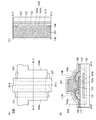
図1に、半導体装置の一形態であるトランジスタ100を示す。トランジスタ100は、トップゲート型のトランジスタである。図1(A)はトランジスタ100の上面図である。また、図1(B)は、図1(A)中の一点鎖線A1−A2で示す部位の断面図であり、図1(C)は、図1(A)中の一点鎖線B1−B2で示す部位の断面図である。また、図1(D)は、図1(B)に示す部位112の拡大図である。なお、トランジスタの構成を理解しやすくするため、図1(A)では、一部の構成要素の記載を省略している。
[1-1. Example of semiconductor device configuration]
FIG. 1 illustrates a
図1に示すトランジスタ100は、絶縁層102上に形成されている。また、絶縁層102は、基板101上に形成されている。トランジスタ100は、積層体103と、低抵抗層114aおよび低抵抗層114bと、ソース電極104aおよびドレイン電極104bと、酸化物層113と、絶縁層106と、ゲート電極107を有する。
The
積層体103は、酸化物層103aと酸化物半導体層103bを有する。ソース電極104aは、低抵抗層114aを介して積層体103と重畳し、ドレイン電極104bは低抵抗層114bを介して積層体103と重畳する。
絶縁層106は、酸化物層113を介して積層体103と重畳する。また、ゲート電極107は、絶縁層106と酸化物層113を介して積層体103と重畳する。
The
The insulating
また、トランジスタ100上に絶縁層108が形成されている。絶縁層108は、トランジスタ100のゲート電極107、絶縁層106、酸化物層113、ソース電極104a、ドレイン電極104b、及び積層体103を覆って形成される。
In addition, an insulating
なお、トランジスタ100のチャネル長Lは、積層体103とゲート電極107が重畳する領域において、積層体103に接する低抵抗層114aの端部と、積層体103に接する低抵抗層114bの端部までの最短距離により決定される(図1(B)参照)。
Note that the channel length L of the
また、この発明を実施するための形態に記載の内容は、適宜組み合わせて用いることができる。 In addition, the contents described in the embodiments for carrying out the present invention can be used in appropriate combination.
〔1−1−1.基板〕
基板101として用いる基板に大きな制限はないが、少なくとも後の加熱処理に耐えうる程度の耐熱性を有していることが必要となる。例えばバリウムホウケイ酸ガラスやアルミノホウケイ酸ガラスなどのガラス基板、セラミック基板、石英基板、サファイア基板などを用いることができる。
[1-1-1. substrate〕
There is no particular limitation on a substrate used as the
また、基板101としてシリコンや炭化シリコンなどの単結晶半導体基板、多結晶半導体基板、シリコンゲルマニウムなどの化合物半導体基板等を用いてもよい。また、SOI基板、半導体基板上に半導体素子が設けられたものなどを用いることができる。
Alternatively, a single crystal semiconductor substrate such as silicon or silicon carbide, a polycrystalline semiconductor substrate, a compound semiconductor substrate such as silicon germanium, or the like may be used as the
なお、基板101として、可撓性基板(フレキシブル基板)を用いてもよい。可撓性基板を用いる場合、可撓性基板上に、トランジスタや容量素子などを直接作製してもよいし、他の作製基板上にトランジスタや容量素子などを作製し、その後可撓性基板に剥離、転置してもよい。なお、作製基板から可撓性基板に剥離、転置するために、作製基板とトランジスタや容量素子などとの間に、剥離層を設けるとよい。
Note that a flexible substrate (flexible substrate) may be used as the
〔1−1−2.下地層〕
絶縁層102は下地層として機能し、基板101からの不純物元素の拡散を防止または低減することができる。絶縁層102は、窒化アルミニウム、酸化アルミニウム、窒化酸化アルミニウム、酸化窒化アルミニウム、酸化マグネシウム酸化ガリウム、窒化シリコン、酸化シリコン、窒化酸化シリコンまたは酸化窒化シリコン、酸化ガリウム、酸化ゲルマニウム、酸化イットリウム、酸化ジルコニウム、酸化ランタン、酸化ネオジム、酸化ハフニウム、酸化タンタルから選ばれた材料を、単層でまたは積層して形成する。なお、本明細書中において、窒化酸化とは、その組成として、酸素よりも窒素の含有量が多いものであって、酸化窒化とは、その組成として、窒素よりも酸素の含有量が多いものを示す。なお、各元素の含有量は、例えば、ラザフォード後方散乱法(RBS:Rutherford Backscattering Spectrometry)等を用いて測定することができる。
[1-1-2. (Underlayer)
The insulating
また、絶縁層102は、スパッタリング法、MBE(Molecular Beam Epitaxy)法、CVD(Chemical Vapor Deposition)、パルスレーザー堆積法(Pulsed Laser Deposition:PLD法)、ALD(Atomic Layer Deposition)法等を適宜用いて形成することができる。また、絶縁層102中の水素の含有量は、好ましくは5×10¹⁹atoms/cm3未満、さらに好ましくは5×1018atoms/cm3未満とする。
The insulating
絶縁層102は、例えば、1層目を窒化シリコン層とし、2層目を酸化シリコン層とした多層膜としてもよい。この場合、酸化シリコン層は酸化窒化シリコン層でも構わない。また、窒化シリコン層は窒化酸化シリコン層でも構わない。酸化シリコン層は、欠陥密度の小さい酸化シリコン層を用いると好ましい。具体的には、電子スピン共鳴(ESR:Electron Spin Resonance)にてg値が2.001のESRスペクトルから算出したスピン密度が3×10¹⁷spins/cm3以下、好ましくは5×1016spins/cm3以下である酸化シリコン層を用いる。
For example, the insulating
また、酸化シリコン層は、過剰酸素を含む酸化シリコン層を用いる。窒化シリコン層は水素およびアンモニアの放出量が少ない窒化シリコン層を用いる。水素、アンモニアの放出量は、昇温脱離ガス分析(TDS:Thermal Desorption Spectrometry)にて測定すればよい。また、窒化シリコン層は、酸素を透過しない、またはほとんど透過しない窒化シリコン層を用いる。 As the silicon oxide layer, a silicon oxide layer containing excess oxygen is used. As the silicon nitride layer, a silicon nitride layer that releases less hydrogen and ammonia is used. The amount of hydrogen and ammonia released may be measured by thermal desorption gas analysis (TDS). As the silicon nitride layer, a silicon nitride layer that does not transmit or hardly transmits oxygen is used.
絶縁層102の厚さは、10nm以上500nm以下、好ましくは50nm以上300nm以下とすればよい。
The thickness of the insulating
なお、本明細書等における「過剰酸素」とは、加熱処理により酸化物層中、酸化物半導体層中、酸化シリコン層中、酸化窒化シリコン層中などを移動可能な酸素、化学量論的組成である酸素より過剰に存在する酸素、または酸素欠損に入り酸素欠損を低減する機能を有する酸素をいう。 Note that “excess oxygen” in this specification and the like means oxygen that can move in an oxide layer, an oxide semiconductor layer, a silicon oxide layer, a silicon oxynitride layer, or the like by heat treatment, a stoichiometric composition, or the like. Oxygen present in excess of oxygen, or oxygen having a function of entering oxygen deficiency and reducing oxygen deficiency.
また、過剰酸素を含む酸化シリコン層とは、加熱処理などによって酸素を放出することができる酸化シリコン層をいう。また、過剰酸素を含む絶縁層は、加熱処理によって酸素を放出する機能を有する絶縁層である。 A silicon oxide layer containing excess oxygen refers to a silicon oxide layer from which oxygen can be released by heat treatment or the like. The insulating layer containing excess oxygen is an insulating layer having a function of releasing oxygen by heat treatment.
ここで、加熱処理によって酸素を放出するとは、TDS分析にて放出される酸素が酸素原子に換算して1×10¹⁸atoms/cm3以上、1×1019atoms/cm3以上または1×1020atoms/cm3以上であることをいう。 Here, oxygen is released by heat treatment means that oxygen released by TDS analysis is converted into oxygen atoms in an amount of 1 × 10 18 atoms / cm 3 or more, 1 × 10 19 atoms / cm 3 or more, or 1 × 10. It means 20 atoms / cm 3 or more.
ここで、TDS分析を用いた酸素の放出量の測定方法について、以下に説明する。 Here, a method of measuring the amount of released oxygen using TDS analysis will be described below.
測定試料をTDS分析したときの気体の全放出量は、放出ガスのイオン強度の積分値に比例する。そして標準試料との比較により、気体の全放出量を計算することができる。 The total amount of gas released when the measurement sample is subjected to TDS analysis is proportional to the integrated value of the ionic strength of the released gas. The total amount of gas released can be calculated by comparison with a standard sample.
例えば、標準試料である所定の密度の水素を含むシリコンウェハのTDS分析結果、および測定試料のTDS分析結果から、測定試料の酸素分子の放出量(NO2)は、数式(1)で求めることができる。ここで、TDS分析で得られる質量数32で検出されるガスの全てが酸素分子由来と仮定する。質量数32のものとしてほかにCH3OHがあるが、存在する可能性が低いものとしてここでは考慮しない。また、酸素原子の同位体である質量数17の酸素原子および質量数18の酸素原子を含む酸素分子についても、自然界における存在比率が極微量であるため考慮しない。 For example, from the TDS analysis result of a silicon wafer containing hydrogen of a predetermined density as a standard sample and the TDS analysis result of the measurement sample, the amount of released oxygen molecules (N O2 ) of the measurement sample is obtained by Equation (1). Can do. Here, it is assumed that all the gases detected by the mass number 32 obtained by the TDS analysis are derived from oxygen molecules. There is CH 3 OH in addition to those having a mass number of 32, but these are not considered here because they are unlikely to exist. In addition, oxygen molecules containing oxygen atoms with a mass number of 17 and oxygen atoms with a mass number of 18 which are isotopes of oxygen atoms are not considered because the existence ratio in nature is extremely small.

NH2は、標準試料から脱離した水素分子を密度で換算した値である。SH2は、標準試料をTDS分析したときのイオン強度の積分値である。ここで、標準試料の基準値を、NH2/SH2とする。SO2は、測定試料をTDS分析したときのイオン強度の積分値である。αは、TDS分析におけるイオン強度に影響する係数である。数式(1)の詳細に関しては、特開平6−275697公報を参照する。なお、上記酸素の放出量は、電子科学株式会社製の昇温脱離分析装置EMD−WA1000S/Wを用い、標準試料として1×1016atoms/cm2の水素原子を含むシリコンウェハを用いて測定した。 N H2 is a value obtained by converting hydrogen molecules desorbed from the standard sample by density. SH2 is an integral value of ion intensity when the standard sample is subjected to TDS analysis. Here, the reference value of the standard sample is N H2 / SH 2 . S O2 is an integrated value of ion intensity when the measurement sample is subjected to TDS analysis. α is a coefficient that affects the ionic strength in the TDS analysis. For details of Equation (1), refer to Japanese Patent Laid-Open No. Hei 6-275697. The oxygen release amount is determined by using a temperature-programmed desorption analyzer EMD-WA1000S / W manufactured by Electronic Science Co., Ltd., and using a silicon wafer containing 1 × 10 16 atoms / cm 2 of hydrogen atoms as a standard sample. It was measured.
また、TDS分析において、酸素の一部は酸素原子として検出される。酸素分子と酸素原子の比率は、酸素分子のイオン化率から算出することができる。なお、上述のαは酸素分子のイオン化率を含むため、酸素分子の放出量を評価することで、酸素原子の放出量についても見積もることができる。 In TDS analysis, part of oxygen is detected as oxygen atoms. The ratio of oxygen molecules to oxygen atoms can be calculated from the ionization rate of oxygen molecules. Note that since the above α includes the ionization rate of oxygen molecules, the amount of released oxygen atoms can be estimated by evaluating the amount of released oxygen molecules.
なお、NO2は酸素分子の放出量である。酸素原子に換算したときの放出量は、酸素分子の放出量の2倍となる。 Note that N 2 O 2 is the amount of released oxygen molecules. The amount of release when converted to oxygen atoms is twice the amount of release of oxygen molecules.
または、加熱処理によって酸素を放出するとは、過酸化ラジカルを含むことをいう。具体的には、過酸化ラジカルに起因するスピン密度が、5×10¹⁷spins/cm3以上であることをいう。なお、過酸化ラジカルを含むとは、ESRにて、g値が2.01近傍に非対称の信号を有することをいう。 Alternatively, releasing oxygen by heat treatment means containing a peroxide radical. Specifically, it means that the spin density resulting from the peroxide radical is 5 × 10 17 spins / cm 3 or more. Note that including a peroxide radical means that an ESR has an asymmetric signal with a g value near 2.01.
または、過剰酸素を含む絶縁層は、酸素が過剰な酸化シリコン(SiOX(X>2))であってもよい。酸素が過剰な酸化シリコン(SiOX(X>2))は、シリコン原子数の2倍より多い酸素原子を単位体積当たりに含むものである。単位体積当たりのシリコン原子数および酸素原子数は、RBSにより測定した値である。 Alternatively, the insulating layer containing excess oxygen may be oxygen-excess silicon oxide (SiO X (X> 2)). Oxygen-excess silicon oxide (SiO X (X> 2)) contains oxygen atoms more than twice the number of silicon atoms per unit volume. The number of silicon atoms and the number of oxygen atoms per unit volume are values measured by RBS.
なお、基板101と、後に設ける積層体103との絶縁性が確保できるようであれば、絶縁層102を設けない構成とすることもできる。
Note that the insulating
〔1−1−3.積層体〕
積層体103は、酸化物層103aと、酸化物層103a上に形成された酸化物半導体層103bを有する。また、酸化物層103aは、絶縁性を示す層であってもよいし、半導体特性を示す層であってもよい。
[1-1-3. (Laminated body)
The
なお、積層体103において、酸化物層103aおよび酸化物半導体層103bに用いる材料によっては、酸化物層103aおよび酸化物半導体層103bの境界を明確に確認できない場合がある。そこで、本発明の一形態を説明する図面では、酸化物層103aと酸化物半導体層103bの境界を破線で表している。
Note that in the
酸化物層103aおよび酸化物半導体層103bは、InもしくはGaの一方、または両方を含む材料で形成する。代表的には、In−Ga酸化物(InとGaを含む酸化物)、In−Zn酸化物(InとZnを含む酸化物)、In−M−Zn酸化物(Inと、元素Mと、Znを含む酸化物。元素Mは、Al、Ti、Ga、Y、Zr、La、Ce、NdまたはHfから選ばれた1種類以上の元素。)がある。
The
また、酸化物半導体層103bに接する酸化物層103aは、酸化物半導体層103bを構成する金属元素のうち、1種類以上の同じ金属元素を含む材料により形成されることが好ましい。このような材料を用いると、酸化物層103aおよび酸化物半導体層103bとの界面に界面準位を生じにくくすることができる。よって、界面におけるキャリアの散乱や捕獲が生じにくく、トランジスタの電界効果移動度を向上させることが可能となる。また、トランジスタのしきい値電圧のばらつきを低減することが可能となる。
The
酸化物層103aおよび酸化物半導体層103bの形成を、途中で大気に曝すことなく、不活性ガス雰囲気、酸化性ガス雰囲気、または減圧下に維持し、連続して行うことにより、酸化物層103aと酸化物半導体層103bとの界面準位をさらに生じにくくすることができる。
The formation of the
酸化物層103aの厚さは、3nm以上100nm以下、好ましくは3nm以上50nm以下とする。また、酸化物半導体層103bの厚さは、3nm以上200nm以下、好ましくは3nm以上100nm以下、さらに好ましくは3nm以上50nm以下とする。
The thickness of the
また、酸化物半導体層103bがIn−M−Zn酸化物であり、酸化物層103aもIn−M−Zn酸化物であるとき、酸化物層103aをIn:M:Zn=x1:y1:z1[原子数比]、酸化物半導体層103bをIn:M:Zn=x2:y2:z2[原子数比]とすると、y1/x1がy2/x2よりも大きくなる酸化物層103aおよび酸化物半導体層103bを選択する。なお、元素MはInよりも酸素との結合力が強い金属元素であり、例えばAl、Ti、Ga、Y、Zr、Sn、La、Ce、NdまたはHfなどが挙げられる。好ましくは、y1/x1がy2/x2よりも1.5倍以上大きくなる酸化物層103aおよび酸化物半導体層103bを選択する。さらに好ましくは、y1/x1がy2/x2よりも2倍以上大きくなる酸化物層103aおよび酸化物半導体層103bを選択する。より好ましくは、y1/x1がy2/x2よりも3倍以上大きくなる酸化物層103aおよび酸化物半導体層103bを選択する。このとき、酸化物半導体層103bにおいて、y1がx1以上であるとトランジスタに安定した電気特性を付与できるため好ましい。ただし、y1がx1の3倍以上になると、トランジスタの電界効果移動度が低下してしまうため、y1はx1と同じか3倍未満であると好ましい。酸化物層103aを上記構成とすることにより、酸化物層103aを、酸化物半導体層103bよりも酸素欠損が生じにくい層とすることができる。
In addition, when the
なお、酸化物層103aがIn−M−Zn酸化物であるとき、InとMの原子数比率は好ましくはInが50atomic%未満、Mが50atomic%以上、さらに好ましくはInが25atomic%未満、Mが75atomic%以上とする。また、酸化物半導体層103bがIn−M−Zn酸化物であるとき、InとMの原子数比率は好ましくはInが25atomic%以上、Mが75atomic%未満、さらに好ましくはInが34atomic%以上、Mが66atomic%未満とする。
Note that when the
例えば、InまたはGaを含む酸化物層103aとしてIn:Ga:Zn=1:3:2、1:3:4、1:3:6、1:6:4、1:9:6、または1:9:0、酸化物半導体層103bとしてIn:Ga:Zn=1:1:1、2:1:4、5:5:6または3:1:2の原子数比のターゲットを用いて形成したIn−Ga−Zn酸化物を用いることができる。なお、酸化物層103aおよび酸化物半導体層103bの原子数比はそれぞれ、誤差として上記の原子数比のプラスマイナス20%の変動を含む。
For example, as the
積層体103を用いたトランジスタに安定した電気特性を付与するためには、酸化物半導体層103b中の不純物及び酸素欠損を低減し、酸化物半導体層103bを真性または実質的に真性と見なせる半導体層とすることが好ましい。また、少なくとも酸化物半導体層103b中のチャネル形成領域が真性または実質的に真性と見なせる半導体層とすることが好ましい。具体的には、酸化物半導体層103bのキャリア密度を、1×10¹⁷/cm3未満、1×1015/cm3未満、または1×1013/cm3未満とする。
In order to impart stable electric characteristics to the transistor including the stacked
酸化物半導体層103bにおいて、水素、窒素、炭素、シリコンなどの、主成分以外の金属元素は不純物となる。酸化物半導体層103b中の不純物を低減するためには、近接する酸化物層103a中および酸化物層113中の不純物も酸化物半導体層103bと同程度まで低減することが好ましい。
In the
特に、酸化物半導体層103bにシリコンが高い濃度で含まれることにより、酸化物半導体層103bにシリコンに起因する不純物準位が形成される。該不純物準位は、トラップとなり、トランジスタの電気特性を劣化させることがある。トランジスタの電気特性の劣化を小さくするためには、酸化物半導体層103bのシリコン濃度を1×10¹⁹atoms/cm3未満、好ましくは5×1018atoms/cm3未満、さらに好ましくは1×1018atoms/cm3未満とすればよい。また、酸化物層103aと酸化物半導体層103bとの界面のシリコン濃度についても、1×1019atoms/cm3未満、好ましくは5×1018atoms/cm3未満、さらに好ましくは1×1018atoms/cm3未満とする。
In particular, when the
また、酸化物半導体層103b中で水素および窒素は、ドナー準位を形成し、キャリア密度を増大させてしまう。酸化物半導体層103bを真性または実質的に真性とするためには、酸化物半導体層103b中の水素濃度は、SIMSにおいて、2×10²⁰atoms/cm3以下、好ましくは5×1019atoms/cm3以下、より好ましくは1×1019atoms/cm3以下、さらに好ましくは5×1018atoms/cm3以下とする。また、窒素濃度は、SIMSにおいて、5×1019atoms/cm3未満、好ましくは5×1018atoms/cm3以下、より好ましくは1×1018atoms/cm3以下、さらに好ましくは5×1017atoms/cm3以下とする。
In addition, hydrogen and nitrogen in the
なお、酸化物半導体層103bにシリコンおよび炭素が高い濃度で含まれることにより、酸化物半導体層103bの結晶性を低下させることがある。酸化物半導体層103bの結晶性を低下させないためには、酸化物半導体層103bのシリコン濃度を1×10¹⁹atoms/cm3未満、好ましくは5×1018atoms/cm3未満、さらに好ましくは1×1018atoms/cm3未満とすればよい。また、酸化物半導体層103bの結晶性を低下させないためには、酸化物半導体層103bの炭素濃度を1×1019atoms/cm3未満、好ましくは5×1018atoms/cm3未満、さらに好ましくは1×1018atoms/cm3未満とすればよい。
Note that when the
ここで、積層体103に含まれる酸化物層103aおよび酸化物半導体層103bの結晶性について説明する。
Here, crystallinity of the
酸化物半導体層103bは、例えば非単結晶を有してもよい。非単結晶は、例えば、CAAC(C Axis Aligned Crystal)、多結晶、微結晶、非晶質を有する。非晶質は、微結晶、CAACよりも欠陥準位密度が高い。また、微結晶は、CAACよりも欠陥準位密度が高い。なお、CAACを有する酸化物半導体を、CAAC−OS(C Axis Aligned Crystalline Oxide Semiconductor)と呼ぶ。
For example, the
酸化物半導体層103bは、例えばCAAC−OSを有してもよい。CAAC−OSは、例えば、c軸配向し、a軸または/およびb軸はマクロに揃っていない酸化物半導体を有している。
For example, the
酸化物半導体層103bは、例えば微結晶を有してもよい。なお、微結晶を有する酸化物半導体を、微結晶酸化物半導体と呼ぶ。微結晶酸化物半導体層は、例えば、1nm以上10nm未満のサイズの微結晶(ナノ結晶ともいう。)を層中に含む。
The
酸化物半導体層103bは、例えば非晶質を有してもよい。なお、非晶質を有する酸化物半導体を、非晶質酸化物半導体と呼ぶ。非晶質酸化物半導体は、例えば、原子配列が無秩序であり、結晶成分を有さない。または、非晶質酸化物半導体は、例えば、完全な非晶質であり、結晶部を有さない。
For example, the
なお、酸化物半導体層103bが、CAAC−OS、微結晶酸化物半導体、非晶質酸化物半導体の混合層であってもよい。混合層は、例えば、非晶質酸化物半導体の領域と、微結晶酸化物半導体の領域と、CAAC−OSの領域と、を有する。また、混合層は、例えば、非晶質酸化物半導体の領域と、微結晶酸化物半導体の領域と、CAAC−OSの領域と、の積層構造を有してもよい。
Note that the
なお、酸化物半導体層103bは、例えば、単結晶を有してもよい。
Note that the
酸化物半導体層103bは、複数の結晶部を有し、当該結晶部のc軸が被形成面の法線ベクトルまたは表面の法線ベクトルに平行な方向に揃っていることが好ましい。なお、異なる結晶部間で、それぞれa軸およびb軸の向きが異なっていてもよい。そのような酸化物半導体層の一例としては、CAAC−OS層がある。
The
CAAC−OS層に含まれる結晶部は、一辺が100nm未満の立方体内に収まる大きさであることが多い。また、透過型電子顕微鏡(TEM:Transmission Electron Microscope)による観察像では、CAAC−OS層に含まれる結晶部と結晶部との境界は明確ではない。また、TEMによってCAAC−OS層には明確な粒界(グレインバウンダリーともいう。)は確認できない。そのため、CAAC−OS層は、粒界に起因する電子移動度の低下が抑制される。 In many cases, a crystal part included in the CAAC-OS layer fits in a cube whose one side is less than 100 nm. Further, in an observation image obtained by a transmission electron microscope (TEM), a boundary between a crystal part and a crystal part included in the CAAC-OS layer is not clear. In addition, a clear grain boundary (also referred to as a grain boundary) cannot be confirmed in the CAAC-OS layer by TEM. Therefore, in the CAAC-OS layer, reduction in electron mobility due to grain boundaries is suppressed.
CAAC−OS層に含まれる結晶部は、例えば、c軸がCAAC−OS膜の被形成面の法線ベクトルまたは表面の法線ベクトルに平行な方向になるように揃い、かつab面に垂直な方向から見て金属原子が三角形状または六角形状に配列し、c軸に垂直な方向から見て金属原子が層状または金属原子と酸素原子とが層状に配列している。なお、異なる結晶部間で、それぞれa軸およびb軸の向きが異なっていてもよい。本明細書において、単に垂直と記載する場合、80°以上100°以下、好ましくは85°以上95°以下の範囲も含まれることとする。また、単に平行と記載する場合、−10°以上10°以下、好ましくは−5°以上5°以下の範囲も含まれることとする。 The crystal part included in the CAAC-OS layer is aligned so that, for example, the c-axis is in a direction parallel to the normal vector of the formation surface of the CAAC-OS film or the normal vector of the surface, and is perpendicular to the ab plane. When viewed from the direction, the metal atoms are arranged in a triangular shape or a hexagonal shape, and when viewed from the direction perpendicular to the c-axis, the metal atoms are arranged in layers, or the metal atoms and oxygen atoms are arranged in layers. Note that the directions of the a-axis and the b-axis may be different between different crystal parts. In this specification, the term “perpendicular” includes a range of 80 ° to 100 °, preferably 85 ° to 95 °. In addition, a simple term “parallel” includes a range of −10 ° to 10 °, preferably −5 ° to 5 °.
なお、CAAC−OS層において、結晶部の分布が一様でなくてもよい。例えば、CAAC−OS層の形成過程において、酸化物半導体層の表面側から結晶成長させる場合、被形成面の近傍に対し表面の近傍では結晶部の占める割合が高くなることがある。また、CAAC−OS層へ不純物を添加することにより、当該不純物添加領域において結晶部の結晶性が低下することもある。 Note that the distribution of crystal parts in the CAAC-OS layer is not necessarily uniform. For example, in the formation process of the CAAC-OS layer, in the case where crystal growth is performed from the surface side of the oxide semiconductor layer, the ratio of crystal parts in the vicinity of the surface is higher in the vicinity of the formation surface. Further, when an impurity is added to the CAAC-OS layer, the crystallinity of the crystal part in the impurity-added region may be decreased.
CAAC−OS層に含まれる結晶部のc軸は、CAAC−OS層の被形成面の法線ベクトルまたは表面の法線ベクトルに平行な方向になるように揃うため、CAAC−OS層の形状(被形成面の断面形状または表面の断面形状)によっては互いに異なる方向を向くことがある。また、結晶部は、成膜したとき、または成膜後に加熱処理などの結晶化処理を行ったときに形成される。即ち、結晶部のc軸は、CAAC−OS層が形成されたときの被形成面の法線ベクトルまたは表面の法線ベクトルに平行な方向になるように揃う。 Since the c-axis of the crystal part included in the CAAC-OS layer is aligned in a direction parallel to the normal vector of the formation surface of the CAAC-OS layer or the normal vector of the surface, the shape of the CAAC-OS layer ( Depending on the cross-sectional shape of the surface to be formed or the cross-sectional shape of the surface, the directions may be different. The crystal part is formed when a film is formed or when a crystallization process such as a heat treatment is performed after the film formation. In other words, the c-axes of the crystal parts are aligned in a direction parallel to the normal vector of the surface where the CAAC-OS layer is formed or the normal vector of the surface.
CAAC−OS層を用いたトランジスタは、可視光や紫外光の照射による電気特性の変動が小さい。よって、当該トランジスタは、信頼性が高い。 In a transistor using a CAAC-OS layer, change in electrical characteristics due to irradiation with visible light or ultraviolet light is small. Therefore, the transistor has high reliability.
酸化物半導体層103bをCAAC−OS層とするためには、酸化物半導体層103bが形成される表面が非晶質であると好ましい。酸化物半導体層103bが形成される表面が結晶質であると、酸化物半導体層103bの結晶性が乱れやすく、CAAC−OS層が形成されにくい。
In order to use the
また、酸化物半導体層103bが形成される表面はCAAC−OS層と同様の結晶質を有していてもよい。酸化物半導体層103bが形成される表面がCAAC−OS層と同様の結晶質を有している場合は、酸化物半導体層103bもCAAC−OS層になりやすい。
Further, the surface over which the
よって、酸化物半導体層103bをCAAC−OS層とするためには、下地である酸化物層103aが非晶質であるか、CAAC−OSと同様の結晶質であると好ましい。
Therefore, in order to make the
〔1−1−4.低抵抗層〕
ソース電極104aと酸化物半導体層103bのオーム接触を実現するために、ソース電極104aと酸化物半導体層103bの間に低抵抗層114aを設ける。また、ドレイン電極104bと酸化物半導体層103bのオーム接触を実現するために、ドレイン電極104bと酸化物半導体層103bの間に低抵抗層114bを設ける。低抵抗層114aおよび低抵抗層114bは、ソース領域およびドレイン領域として機能させることができる。
[1-1-4. (Low resistance layer)
In order to achieve ohmic contact between the
低抵抗層114aおよび低抵抗層114bは、酸化物半導体層103bに接して形成する。低抵抗層114aおよび低抵抗層114bは、導電性を有する酸化物材料、または酸化しても導電性を有する材料で形成する。具体的には、低抵抗層114aおよび低抵抗層114bの抵抗率は、好ましくは500μΩ・cm以下、より好ましくは100μΩ・cm以下、さらに好ましくは50μΩ・cm以下である。
The
また、低抵抗層114aおよび低抵抗層114bは、酸化物半導体層103bよりも仕事関数が小さいことが好ましい。また、低抵抗層114aおよび低抵抗層114bは、酸化物半導体層103bよりも電子親和力が大きいことが好ましい。
The
また、低抵抗層114aおよび低抵抗層114bは、酸化物半導体層103bを構成する金属元素のうち、1種類以上の同じ金属元素を含む材料により形成されることが好ましい。
The
例えば、酸化物半導体層103bにInとZnを含む酸化物を用いる場合、低抵抗層114aおよび低抵抗層114bは、InもしくはZnの一方、または両方を含む材料で形成する。具体的には、In、Zn、In−Zn合金、In酸化物、Zn酸化物、In−Zn酸化物、In−Ga酸化物(InとGaを含む酸化物)、In−Zn酸化物(InとZnを含む酸化物)、In−Sn酸化物(InとSnを含む酸化物)、In−M−Zn酸化物(Inと、元素Mと、Znを含む酸化物。元素Mは、Al、Ti、Ga、Y、Zr、La、Ce、NdまたはHfから選ばれた1種類以上の元素。)などがある。
For example, in the case where an oxide containing In and Zn is used for the
低抵抗層114aおよび低抵抗層114bの厚さは、3nm以上100nm以下、好ましくは3nm以上50nm以下とする。
The thickness of the
なお、低抵抗層114aおよび低抵抗層114bがIn−M−Zn酸化物であるとき、InとMの原子数比率は好ましくはInが50atomic%以上、Mが50atomic%未満、さらに好ましくはInが75atomic%以上、Mが25atomic%未満とする。
Note that when the low-
例えば、InまたはGaを含む低抵抗層114aおよび低抵抗層114bとして、In:Ga:Zn=2:1:1、3:1:2、6:1:4の原子数比のターゲットを用いて形成したIn−Ga−Zn酸化物や、酸化インジウム、酸化亜鉛などを用いることができる。なお、上記原子数比はそれぞれ、誤差として上記の原子数比のプラスマイナス20%の変動を含む。
For example, as the low-
なお、ソース電極104aおよびドレイン電極104bを積層体103の一部から酸素を奪い酸素欠損を生じさせることが可能な材料で形成し、該電極と積層体103を直接接触させることでオーム接触を実現することも可能である。この場合、積層体103中の酸素欠損が生じた領域はキャリア濃度が増加し、当該領域はn型化し、n型領域(n+層)となる。したがって、当該領域はソース領域およびドレイン領域として作用させることができる。積層体103から酸素を奪い、酸素欠損を生じさせることが可能な材料の一例として、タングステン、チタン等を挙げることができる。
Note that the
また、イオンインプランテーション法などを用いて、積層体103中に、水素などのドナーとなる不純物元素や、希ガス元素などを導入してn型領域を形成することもできる。水素は酸化物半導体層中でドナーとなるため、水素を導入することによりキャリア濃度を増加させることができる。また、希ガス元素の導入は、導入時のエネルギーにより酸化物半導体層中に酸素欠損を生じさせ、キャリア濃度を増加させることができる。
Alternatively, an n-type region can be formed by introducing an impurity element serving as a donor such as hydrogen, a rare gas element, or the like into the
しかしながら、積層体103の一部から酸素を奪いn型領域を形成する方法では、積層体103中に形成される酸素欠損量の制御が難しく、形成されるn型領域(ソース領域およびドレイン領域)の大きさや抵抗値のばらつきが大きくなりやすい。また、積層体103に酸素を供給して酸素欠損を低減し、特に酸化物半導体層103b中のチャネル形成領域を真性または実質的に真性な酸化物半導体層とする工程では、チャネル形成領域のみに酸素を供給することが困難である。
However, in the method of removing oxygen from a part of the
このため、積層体103中に酸素を供給して酸素欠損を低減する工程において、積層体103の一部に形成されたn型領域中の酸素欠損も低減されるため、n型領域の抵抗値が大きくなり、また、n型領域の抵抗値のばらつきも大きくなってしまう。
Therefore, in the step of supplying oxygen into the
また、酸素の供給によりn型領域の酸素欠損量が変動すると、n型領域の大きさも変動する恐れがある。n型領域の大きさの変動は、実質的にトランジスタのチャネル長の変動に繋がり、特性ばらつきを増加させる一因となる。その影響は、特にチャネル長が1μm以下のトランジスタにおいて顕著となりやすい。 Further, when the oxygen deficiency in the n-type region varies due to the supply of oxygen, the size of the n-type region may also vary. Variation in the size of the n-type region substantially leads to variation in the channel length of the transistor, and contributes to an increase in characteristic variation. The influence is particularly prominent in a transistor having a channel length of 1 μm or less.
ここで、酸化物半導体層の一部から酸素を奪いn型領域を形成する方法においてチャネル長が変動する現象について、図14に示すトランジスタ900を用いて説明しておく。また、図14(B1)乃至図14(B3)は、図14(A)中の部位920の拡大図である。
Here, a phenomenon in which the channel length fluctuates in a method for removing oxygen from part of an oxide semiconductor layer to form an n-type region will be described with reference to a
図14(A)は、トランジスタ900の構成を示す断面図である。トランジスタ900は、基板901上に絶縁層902を介して形成されている。また、トランジスタ900は酸化物半導体層903を有し、酸化物半導体層903の一部に接するソース電極904a、ドレイン電極904bを有する。また、ゲート電極907が、絶縁層906を介して酸化物半導体層903と重畳している。
FIG. 14A is a cross-sectional view illustrating the structure of the
ソース電極904aおよびドレイン電極904bは、酸化物半導体層903の一部から酸素を奪い、酸化物半導体層903に酸素欠損を生じさせることが可能な材料で形成されている。よって、酸化物半導体層903の、ソース電極904a、およびドレイン電極904bが接する領域近傍がn型化し、低抵抗層914aおよび低抵抗層914bが形成される。
The source electrode 904 a and the
図14(B1)は、ソース電極904aおよび低抵抗層914aの端部が揃っている場合の部位920の拡大図である。この時のチャネル長をLとする。ソース電極904aが、酸化物半導体層903から酸素を奪う材料で形成されている場合、低抵抗層914aの端部がソース電極904aの端部を越えて広がってしまう場合がある(図14(B2)参照。)。なお、図示していないが、ドレイン電極904bの端部においても、ソース電極904aの端部と同様の現象が生じる。よって、以下の説明では、ドレイン電極904bの端部についての説明を省略している。
FIG. 14B1 is an enlarged view of the
低抵抗層914aの端部がソース電極904aの端部を越えて広がった距離をdLとすると、その時のチャネル長L’は、チャネル長L−2×dLとなる。なお、dLは、この後の作製条件により変動する。よって、トランジスタの電気特性のばらつきは、dLのばらつきにより増大する。
When the distance that the end of the
また、上述したように、酸化物半導体層903のチャネル形成領域を真性半導体とするために酸素を供給する工程では、低抵抗層914a中の酸素欠損も低減される。よって、低抵抗層914aが縮小し、抵抗値や、抵抗値のばらつきが大きくなってしまう(図14(B3)参照。)。
In addition, as described above, oxygen vacancies in the low-
なお、酸化物半導体層903を積層体103に置き換えても同様の現象が生じる。
Note that the same phenomenon occurs even when the
また、イオンインプランテーション法などを用いて、n型領域を形成する方法においても、同様の問題を有している。例えば、水素は拡散しやすいため、形成されるn型領域の抵抗値のばらつきが大きくなりやすく、n型領域の大きさの変動も生じやすい。また、希ガス元素導入時のエネルギーにより酸素欠損を生じさせる方法は、積層体103に酸素欠損を生じさせることが可能な材料を接触させる場合と同様の問題を有する。
In addition, a method for forming an n-type region using an ion implantation method or the like has a similar problem. For example, since hydrogen easily diffuses, variation in resistance value of the n-type region to be formed is likely to increase, and the size of the n-type region is likely to vary. Further, the method of generating oxygen vacancies by the energy at the time of introducing a rare gas element has the same problem as the case where a material capable of causing oxygen vacancies is brought into contact with the
このように、n型領域では不純物または酸素欠損の増加が求められ、チャネル形成領域では、不純物または酸素欠損の低減が求められている。 Thus, an increase in impurities or oxygen vacancies is required in the n-type region, and a reduction in impurities or oxygen vacancies is required in the channel formation region.
本発明の一態様では、ソース電極104aおよびドレイン電極104bを、上記材料により形成された低抵抗層114aおよび低抵抗層114bを介して積層体103と接続するため、上記の相反する要求を満たすことが可能となる。
In one embodiment of the present invention, the
上記に例示した低抵抗層114aおよび低抵抗層114bに用いる材料は、酸素が供給されても抵抗値を一定範囲内に保つことができる。すなわち、酸化物半導体層103b中の酸素欠損を低減するための酸素が低抵抗層114aおよび低抵抗層114bに供給されても、低抵抗層114aおよび低抵抗層114bをソース領域およびドレイン領域として安定して作用させることができる。よって、チャネルが形成される半導体層の真性化と、安定したソース領域およびドレイン領域の形成を実現することができる。また、本発明の一態様によれば、過剰酸素によるソース領域およびドレイン領域の大きさの変動も生じにくいため、トランスタのチャネル長が変動しにくい。よって、電気特性が良好で、電気特性のばらつきが少なく、信頼性のよいトランジスタを実現できる。
The materials used for the
〔1−1−5.ソース電極・ドレイン電極〕
ソース電極104a及びドレイン電極104bは、低抵抗層114aおよび低抵抗層114bを介して積層体103上に形成される。ソース電極104a及びドレイン電極104bを形成するための導電性材料としては、アルミニウム、クロム、銅、銀、金、白金、タンタル、ニッケル、チタン、モリブデン、タングステン、ハフニウム(Hf)、バナジウム(V)、ニオブ(Nb)、マンガン、マグネシウム、ジルコニウム、ベリリウム等から選ばれた金属元素、上述した金属元素を成分とする合金、または上述した金属元素を組み合わせた合金などを用いることができる。また、リン等の不純物元素を含有させた多結晶シリコンに代表される半導体、ニッケルシリサイドなどのシリサイドを用いてもよい。導電層の形成方法は特に限定されず、蒸着法、CVD法、スパッタリング法、スピンコート法などの各種形成方法を用いることができる。
[1-1-5. (Source electrode / drain electrode)
The
また、ソース電極104a及びドレイン電極104bは、積層体103の一部から酸素を奪いにくく酸素欠損を生じさせにくい導電性材料を用いて形成することが好ましい。このような材料としては、窒化タンタル、窒化チタン、酸化チタンなどの、導電性を有する金属窒化物、または導電性を有する金属酸化物などを用いることができる。なお、酸素を奪いにくい導電性材料には、酸素と結合しにくい導電性材料や、酸素が拡散しにくい材料も含まれる。
The
ソース電極104a及びドレイン電極104bを、酸素欠損を生じさせない導電性材料を用いて形成することにより、低抵抗層114aおよび低抵抗層114bの抵抗値を安定させることができる。また、低抵抗層114aや低抵抗層114bを介して積層体103中の酸素が引き抜かれることを防ぐことができる。
By forming the
また、ソース電極104a及びドレイン電極104bは、インジウム錫酸化物(以下、「ITO」ともいう。)、酸化タングステンを含むインジウム酸化物、酸化タングステンを含むインジウム亜鉛酸化物、酸化チタンを含むインジウム酸化物、酸化チタンを含むインジウム錫酸化物、インジウム亜鉛酸化物、酸化ケイ素を添加したインジウム錫酸化物などの酸素を含む導電性材料を適用することもできる。また、上記酸素を含む導電性材料と、上記金属元素を含む材料の積層構造とすることもできる。
The
ソース電極104a及びドレイン電極104bは、単層構造でも、二層以上の積層構造としてもよい。例えば、シリコンを含むアルミニウム層の単層構造、アルミニウム層上にチタン層を積層する二層構造、窒化チタン層上にチタン層を積層する二層構造、窒化チタン層上にタングステン層を積層する二層構造、窒化タンタル層上にタングステン層を積層する二層構造、チタン層と、そのチタン層上にアルミニウム層を積層し、さらにその上にチタン層を形成する三層構造などがある。また、アルミニウムに、チタン、タンタル、タングステン、モリブデン、クロム、ネオジム、スカンジウムから選ばれた元素の層、または複数組み合わせた合金層、もしくは窒化物層を用いてもよい。
The
ソース電極104a及びドレイン電極104bを二層以上の積層構造とする場合は、少なくとも低抵抗層114aおよび低抵抗層114bと接する側の層を、酸素欠損を生じさせない導電性材料を用いて形成することが好ましい。
In the case where the
なお、ソース電極104a及びドレイン電極104bの厚さは、10nm以上500nm以下、好ましくは50nm以上300nm以下とすればよい。
Note that the thickness of the
〔1−1−6.積層体に接する酸化物層およびゲート絶縁層〕
酸化物層113は、積層体103と同様の材料及び方法で形成される。酸化物層113は、ソース電極104a、ドレイン電極104b、及び積層体103の一部に接して形成される。このため、酸化物層113は、酸化物層113が接する積層体103と同様の材料、または、積層体103を構成する金属元素のうち1種類以上の同じ金属元素を含む材料により形成されることが好ましい。このような材料を用いると、酸化物層113と積層体103の界面に順位が存在しないか、ほとんどない状態とすることができる。また、酸化物層113は、酸化物層103aと同様の材料及び方法で形成することが好ましい。
[1-1-6. (Oxide layer and gate insulating layer in contact with stack)
The
なお、酸化物層113に用いる材料によっては、酸化物層113と積層体103の境界を明確に確認できない場合がある。そこで、本発明の一形態を説明する図面では、酸化物層113と積層体103の境界を破線で表している。
Note that depending on the material used for the
また、酸化物層113をソース電極104aおよびドレイン電極104b上に設けることで、外部から浸入した水等の不純物が積層体103に到達しにくくすることができる。また、酸化物層113をソース電極104aおよびドレイン電極104b上に設けることで、ソース電極104aおよびドレイン電極104bを、Cuなどの拡散しやすい金属元素を含んで形成しても、該元素の拡散を防ぐことができる。
In addition, by providing the
また、図1(A)中の一点鎖線B1−B2で示す部位では、積層体103の表面および側面が酸化物層113に覆われている(図1(C)参照)。
1A, the surface and side surfaces of the
絶縁層106は、ゲート絶縁層として機能する。酸化物層113上に形成される絶縁層106は、酸化アルミニウム、酸化マグネシウム、酸化シリコン、酸化窒化シリコン、窒化酸化シリコン、窒化シリコン、酸化ガリウム、酸化ゲルマニウム、酸化イットリウム、酸化ジルコニウム、酸化ランタン、酸化ネオジム、酸化ハフニウムおよび酸化タンタルのうち、一種以上含む材料を、単層でまたは積層して形成する。絶縁層106の厚さは、1nm以上100nm以下、好ましくは10nm以上50nm以下とする。絶縁層106は、スパッタリング法、CVD法、MBE法、ALD法またはPLD法を用いて形成することができる。
The insulating
絶縁層106は、例えば、1層目を窒化シリコン層とし、2層目を酸化シリコン層とした多層膜としてもよい。この場合、酸化シリコン層は酸化窒化シリコン層でも構わない。また、窒化シリコン層は窒化酸化シリコン層でも構わない。酸化シリコン層は、欠陥密度の小さい酸化シリコン層を用いると好ましい。具体的には、ESRにてg値が2.001の信号に由来するスピンのスピン密度が3×10¹⁷spins/cm3以下、好ましくは5×1016spins/cm3以下である酸化シリコン層を用いる。また、酸化シリコン層は、過剰酸素を含む酸化シリコン層を用いると好ましい。窒化シリコン層は水素およびアンモニアの放出量が少ない窒化シリコン層を用いる。水素、アンモニアの放出量は、TDS分析にて測定すればよい。
For example, the insulating
また、一般に、容量素子は対向する二つの電極の間に誘電体を挟む構成を有し、誘電体の厚さが薄いほど(対向する二つの電極間距離が短いほど)、また、誘電体の誘電率が大きいほど容量値が大きくなる。ただし、容量素子の容量値を増やすために誘電体を薄くすると、トンネル効果などに起因して、二つの電極間に生じる漏れ電流(以下、「リーク電流」ともいう)が増加しやすくなり、また、容量素子の絶縁耐圧が低下しやすくなる。 In general, the capacitive element has a configuration in which a dielectric is sandwiched between two opposing electrodes. The thinner the dielectric (the shorter the distance between the two opposing electrodes), the more the dielectric As the dielectric constant increases, the capacitance value increases. However, if the dielectric is thinned to increase the capacitance value of the capacitive element, the leakage current generated between the two electrodes (hereinafter also referred to as “leakage current”) tends to increase due to the tunnel effect, etc. In addition, the withstand voltage of the capacitive element tends to decrease.
トランジスタのゲート電極、ゲート絶縁層、半導体層が重畳する部分は、前述した容量素子として機能する(以下、「ゲート容量」ともいう)。なお、半導体層の、ゲート絶縁層を介してゲート電極と重畳する領域にチャネルが形成される。すなわち、ゲート電極とチャネル形成領域が容量素子の二つの電極として機能し、ゲート絶縁層が容量素子の誘電体として機能する。ゲート容量の容量値は大きいほうが好ましいが、容量値を大きくするためにゲート絶縁層を薄くすると、前述のリーク電流の増加や、絶縁耐圧の低下といった問題が生じやすい。 A portion where the gate electrode, the gate insulating layer, and the semiconductor layer of the transistor overlap functions as the above-described capacitor (hereinafter also referred to as “gate capacitor”). Note that a channel is formed in the semiconductor layer in a region overlapping with the gate electrode with the gate insulating layer interposed therebetween. That is, the gate electrode and the channel formation region function as two electrodes of the capacitor, and the gate insulating layer functions as a dielectric of the capacitor. Although it is preferable that the capacitance value of the gate capacitance is large, if the gate insulating layer is thinned in order to increase the capacitance value, problems such as an increase in leakage current and a decrease in dielectric strength are likely to occur.
そこで、絶縁層106として、ハフニウムシリケート(HfSixOy(x>0、y>0))、窒素が添加されたハフニウムシリケート(HfSixOyNz(x>0、y>0、z>0))、窒素が添加されたハフニウムアルミネート(HfAlxOyNz(x>0、y>0、z>0))、酸化ハフニウム、酸化イットリウムなどのhigh−k材料を用いると、絶縁層106を厚くしても、ゲート電極107と積層体103間の容量値を十分確保することが可能となる。
Therefore, as the insulating
例えば、絶縁層106として誘電率が大きいhigh−k材料を用いると、絶縁層106を厚くしても、絶縁層106に酸化シリコンを用いた場合と同等の容量値を実現できるため、ゲート電極107と積層体103間に生じるリーク電流を低減できる。また、ゲート電極107と同じ層を用いて形成された配線と、該配線と重畳する他の配線との間に生じるリーク電流を低減できる。なお、絶縁層106をhigh−k材料と、上記材料との積層構造としてもよい。
For example, when a high-k material having a high dielectric constant is used for the insulating
なお、酸化物層113もゲート絶縁層の一部と見なすこともできる。また、酸化物層113と絶縁層106を積層することで、ソース電極104a及びドレイン電極104bと、ゲート電極107間の絶縁耐電圧を向上させることができる。よって、信頼性のよい半導体装置を実現できる。
Note that the
〔1−1−7.ゲート電極〕
ゲート電極107を形成するための導電性材料としては、アルミニウム、クロム、銅、銀、金、白金、タンタル、ニッケル、チタン、モリブデン、タングステン、ハフニウム(Hf)、バナジウム(V)、ニオブ(Nb)、マンガン、マグネシウム、ジルコニウム、ベリリウム等から選ばれた金属元素、上述した金属元素を成分とする合金、または上述した金属元素を組み合わせた合金などを用いることができる。また、リン等の不純物元素を含有させた多結晶シリコンに代表される半導体、ニッケルシリサイドなどのシリサイドを用いてもよい。導電層の形成方法は特に限定されず、蒸着法、CVD法、スパッタリング法、スピンコート法などの各種形成方法を用いることができる。
[1-1-7. (Gate electrode)
As a conductive material for forming the
また、ゲート電極107は、インジウム錫酸化物、酸化タングステンを含むインジウム酸化物、酸化タングステンを含むインジウム亜鉛酸化物、酸化チタンを含むインジウム酸化物、酸化チタンを含むインジウム錫酸化物、インジウム亜鉛酸化物、酸化ケイ素を添加したインジウム錫酸化物などの酸素を含む導電性材料を適用することもできる。また、上記酸素を含む導電性材料と、上記金属元素を含む材料の積層構造とすることもできる。
The
ゲート電極107は、単層構造でも、二層以上の積層構造としてもよい。例えば、シリコンを含むアルミニウム層の単層構造、アルミニウム層上にチタン層を積層する二層構造、窒化チタン層上にチタン層を積層する二層構造、窒化チタン層上にタングステン層を積層する二層構造、窒化タンタル層上にタングステン層を積層する二層構造、チタン層と、そのチタン層上にアルミニウム層を積層し、さらにその上にチタン層を形成する三層構造などがある。また、アルミニウムに、チタン、タンタル、タングステン、モリブデン、クロム、ネオジム、スカンジウムから選ばれた元素の層、または複数組み合わせた合金層、もしくは窒化物層を用いてもよい。
The
また、ゲート電極107と絶縁層106との間に、In−Ga−Zn酸窒化物半導体層、In−Sn酸窒化物半導体層、In−Ga酸窒化物半導体層、In−Zn酸窒化物半導体層、Sn酸窒化物半導体層、In酸窒化物半導体層、金属窒化物(InN、ZnN等)層等を設けてもよい。これらは5eV以上の仕事関数を有し、酸化物半導体の電子親和力よりも大きい値を有するため、チャネルが形成される半導体層に酸化物半導体を用いたトランジスタのしきい値電圧を正の電圧の方向に変動させることができ、所謂ノーマリーオフ特性のスイッチング素子を実現できる。例えば、ゲート電極107と絶縁層106との間に、In−Ga−Zn酸窒化物半導体層を設ける場合、少なくとも酸化物半導体層103bより高い窒素濃度、具体的には窒素濃度が7原子%以上のIn−Ga−Zn酸窒化物半導体層を設ける。
Further, an In—Ga—Zn oxynitride semiconductor layer, an In—Sn oxynitride semiconductor layer, an In—Ga oxynitride semiconductor layer, and an In—Zn oxynitride semiconductor are provided between the
なお、ゲート電極107の厚さは、10nm以上500nm以下、好ましくは50nm以上300nm以下とすればよい。
Note that the thickness of the
〔1−1−8.保護絶縁層〕
絶縁層108は、保護絶縁層として機能し、外部からの不純物元素の拡散を防止または低減することができる。絶縁層108は、絶縁層102と同様の材料及び方法で形成することができる。例えば、絶縁層108として酸化アルミニウムを用いてもよい。
[1-1-8. (Protective insulation layer)
The insulating
なお、絶縁層108の厚さは、10nm以上300nm以下、好ましくは30nm以上200nm以下とすればよい。
Note that the thickness of the insulating
また、図2(A)に示すように、絶縁層108上に、さらに絶縁層109を形成してもよいし、図2(B)に示すように、絶縁層108とゲート電極107の間に絶縁層109を形成してもよい。絶縁層109としては、絶縁層102と同様の材料、または低誘電率材料(low−k材料)を用いることができる。
In addition, an insulating
なお、絶縁層109の厚さは、10nm以上500nm以下、好ましくは30nm以上300nm以下とすればよい。
Note that the thickness of the insulating
また、図3(A)および図3(B)に示すように、絶縁層109の表面に平坦化処理を行うことで、トランジスタに起因する絶縁層109表面の凹凸を低減することができる。平坦化処理としては、化学的機械研磨(CMP:Chemical Mechanical Polishing、以下CMP処理という)などの研磨処理の他に、エッチング処理などを適用することも可能である。また、CMP処理とエッチング処理を組み合わせて行ってもよい。絶縁層109表面の凹凸を低減することで、絶縁層109よりも上層に形成される層の被覆性を向上することができる。
In addition, as illustrated in FIGS. 3A and 3B, unevenness on the surface of the insulating
なお、絶縁層109を、平坦化機能を有する材料で形成してもよい。平坦化機能を有する材料には、例えば、ポリイミド、アクリル樹脂、ベンゾシクロブテン系樹脂等の有機材料を用いることができる。絶縁層109に平坦化機能を有する材料を用いることで、平坦化処理を省略しても、絶縁層109表面の凹凸を低減することができる。
Note that the insulating
絶縁層109の表面に平坦化処理を行った場合、または、絶縁層109を平坦化機能を有する材料で形成した場合、絶縁層109の最大厚さは、100nm以上5μm以下、好ましくは200nm以上3μm以下とすればよい。
In the case where the surface of the insulating
絶縁層102、絶縁層106、及び絶縁層108の少なくともいずれかが過剰酸素を含む絶縁層を含む場合、過剰酸素によって酸化物半導体層103bの酸素欠損を低減することができる。
In the case where at least one of the insulating
〔1−2.半導体装置の作製方法例〕
半導体装置の作製方法の一例として、図4に示す断面図を用いてトランジスタ100の作製方法の一例を説明する。
[1-2. Example of manufacturing method of semiconductor device]
As an example of a method for manufacturing a semiconductor device, an example of a method for manufacturing the
〔1−2−1.下地層の形成〕
基板101上に下地層として機能する絶縁層102を形成する。ここでは、基板101としてガラス基板を用いる。次に、絶縁層102を、窒化シリコン層と、第1の酸化シリコン層と、第2の酸化シリコン層の積層構造とする場合について例示する。
[1-2-1. Formation of underlayer]
An insulating
まず、基板101上に窒化シリコン層を形成する。窒化シリコン層は、CVD法の一種であるプラズマCVD法によって形成することが好ましい。具体的には、基板温度を180℃以上400℃以下、好ましくは200℃以上370℃以下とし、シリコンを含む堆積性ガス、窒素ガスおよびアンモニアガスを用いて圧力20Pa以上250Pa以下、好ましくは40Pa以上200Pa以下として、高周波電力を供給することで成膜すればよい。
First, a silicon nitride layer is formed on the
なお、窒素ガスの流量はアンモニアガスの流量の5倍以上50倍以下、好ましくは10倍以上50倍以下とする。なお、アンモニアガスを用いることで、シリコンを含む堆積性ガスおよび窒素ガスの分解を促すことができる、これは、アンモニアガスがプラズマエネルギーおよび熱エネルギーによって解離し、解離することで生じるエネルギーが、シリコンを含む堆積性ガスの結合、および窒素ガスの結合の分解に寄与するためである。 Note that the flow rate of nitrogen gas is 5 to 50 times, preferably 10 to 50 times the flow rate of ammonia gas. Note that by using ammonia gas, it is possible to promote the decomposition of the deposition gas containing nitrogen and nitrogen gas. This is because the energy generated by the dissociation of ammonia gas by the plasma energy and the thermal energy is the silicon. This is to contribute to the decomposition of the bonding of the deposition gas containing nitrogen and the bonding of the nitrogen gas.
従って、上述の方法によって、水素ガスおよびアンモニアガスの放出量が少ない窒化シリコン層を成膜することができる。また、水素の含有量が少ないため、緻密となり、水素、水および酸素を透過しない、またはほとんど透過しない窒化シリコン層を形成することができる。 Therefore, a silicon nitride layer with a small release amount of hydrogen gas and ammonia gas can be formed by the above-described method. In addition, since the content of hydrogen is small, a silicon nitride layer that is dense and hardly or hardly transmits hydrogen, water, and oxygen can be formed.
次に、第1の酸化シリコン層を形成する。第1の酸化シリコン層は、プラズマCVD法によって形成することが好ましい。具体的には、基板温度を160℃以上350℃以下、好ましくは180℃以上260℃以下とし、シリコンを含む堆積性ガスおよび酸化性ガスを用いて圧力100Pa以上250Pa以下、好ましくは100Pa以上200Pa以下として、電極に0.17W/cm2以上0.5W/cm2以下、好ましくは0.25W/cm2以上0.35W/cm2以下の高周波電力を供給することで成膜する。 Next, a first silicon oxide layer is formed. The first silicon oxide layer is preferably formed by a plasma CVD method. Specifically, the substrate temperature is set to 160 ° C. to 350 ° C., preferably 180 ° C. to 260 ° C., and a pressure of 100 Pa to 250 Pa, preferably 100 Pa to 200 Pa using a deposition gas and an oxidizing gas containing silicon. as the electrode to 0.17 W / cm 2 or more 0.5 W / cm 2 or less, preferably deposited by supplying the following high-frequency power 0.25 W / cm 2 or more 0.35 W / cm 2.
上述の方法によれば、プラズマ中でのガスの分解効率が高まり、酸素ラジカルが増加し、ガスの酸化が進むため、過剰酸素を含む第1の酸化シリコン層を成膜することができる。 According to the above-described method, the efficiency of gas decomposition in plasma increases, oxygen radicals increase, and gas oxidation proceeds. Therefore, the first silicon oxide layer containing excess oxygen can be formed.
続いて、第2の酸化シリコン層を形成する。第2の酸化シリコン層は、プラズマCVD法によって形成することが好ましい。具体的には、基板温度を180℃以上400℃以下、好ましくは200℃以上370℃以下とし、シリコンを含む堆積性ガスおよび酸化性ガスを用いて圧力20Pa以上250Pa以下、好ましくは40Pa以上200Pa以下として、電極に高周波電力を供給することで形成する。なお、シリコンを含む堆積性ガスの代表例としては、シラン、ジシラン、トリシラン、フッ化シラン、などがある。酸化性ガスとしては、酸素、オゾン、亜酸化窒素、二酸化窒素などがある。 Subsequently, a second silicon oxide layer is formed. The second silicon oxide layer is preferably formed by a plasma CVD method. Specifically, the substrate temperature is set to 180 ° C. or higher and 400 ° C. or lower, preferably 200 ° C. or higher and 370 ° C. or lower, and a pressure of 20 Pa or higher and 250 Pa or lower, preferably 40 Pa or higher and 200 Pa or lower, using a deposition gas and an oxidizing gas containing silicon. As described above, the high-frequency power is supplied to the electrodes. Note that typical examples of the deposition gas containing silicon include silane, disilane, trisilane, and fluorinated silane. Examples of the oxidizing gas include oxygen, ozone, nitrous oxide, and nitrogen dioxide.
なお、シリコンを含む堆積性ガスに対する酸化性ガスの流量を100倍以上とすることで、第2の酸化シリコン層中の水素含有量を低減し、かつダングリングボンドを低減することができる。 Note that when the flow rate of the oxidizing gas with respect to the deposition gas containing silicon is 100 times or more, the hydrogen content in the second silicon oxide layer can be reduced and dangling bonds can be reduced.
以上のようにして、第1の酸化シリコン層よりも欠陥密度の小さい第2の酸化シリコン層を成膜する。即ち、第2の酸化シリコン層は、ESRにてg値が2.001の信号に由来するスピンの密度が3×10¹⁷spins/cm3以下、または5×1016spins/cm3以下とすることができる。 As described above, the second silicon oxide layer having a defect density lower than that of the first silicon oxide layer is formed. That is, in the second silicon oxide layer, the density of spins derived from a signal having a g value of 2.001 in ESR is 3 × 10 17 spins / cm 3 or less, or 5 × 10 16 spins / cm 3 or less. be able to.
また、窒化シリコン層形成後に、窒化シリコン層に酸素を添加する処理を行ってもよい。また、第1の酸化シリコン層後に、第1の酸化シリコン層に酸素を添加する処理を行ってもよい。また、第2の酸化シリコン層後に、第2の酸化シリコン層に酸素を添加する処理を行ってもよい。酸素を添加する処理は、イオンドーピング装置またはプラズマ処理装置を用いて行うことができる。また、イオンドーピング装置として、質量分離機能を有するイオンドーピング装置を用いてもよい。酸素を添加するためのガスとしては、16O2もしくは18O2などの酸素ガス、亜酸化窒素ガスまたはオゾンガスなどを用いることができる。 Further, after the silicon nitride layer is formed, treatment for adding oxygen to the silicon nitride layer may be performed. Further, after the first silicon oxide layer, treatment for adding oxygen to the first silicon oxide layer may be performed. Further, after the second silicon oxide layer, treatment for adding oxygen to the second silicon oxide layer may be performed. The treatment for adding oxygen can be performed using an ion doping apparatus or a plasma treatment apparatus. Further, an ion doping apparatus having a mass separation function may be used as the ion doping apparatus. As a gas for adding oxygen, oxygen gas such as 16 O 2 or 18 O 2 , nitrous oxide gas, ozone gas, or the like can be used.
〔1−2−2.積層体および低抵抗層の形成〕
次に、絶縁層102上に、酸化物層103aおよび酸化物半導体層103bを含む積層体103と、低抵抗層114aおよび低抵抗層114bを形成するための低抵抗層114を設ける。積層体103および低抵抗層114は、スパッタリング法、塗布法、パルスレーザー堆積法、レーザーアブレーション法等を用いて形成することができる。
[1-2-2. Formation of laminate and low resistance layer]
Next, the
スパッタリング法でIn若しくはGaを含む酸化物層103a、酸化物半導体層103b、低抵抗層114を形成する場合、プラズマを発生させるための電源装置は、RF電源装置、AC電源装置、DC電源装置等を適宜用いることができる。
When the
スパッタリングガスは、希ガス(代表的にはアルゴン)、酸素、希ガス及び酸素の混合ガスを適宜用いる。なお、希ガス及び酸素の混合ガスの場合、希ガスに対して酸素のガス比を高めることが好ましい。スパッタリングガスは不純物濃度の少ないガスを用いる。具体的には、露点が−40℃以下、好ましくは−60℃以下であるスパッタリングガスを用いることが好ましい。 As the sputtering gas, a rare gas (typically argon), oxygen, a rare gas, and a mixed gas of oxygen are used as appropriate. Note that in the case of a mixed gas of a rare gas and oxygen, it is preferable to increase the gas ratio of oxygen to the rare gas. As the sputtering gas, a gas having a low impurity concentration is used. Specifically, it is preferable to use a sputtering gas having a dew point of −40 ° C. or lower, preferably −60 ° C. or lower.
また、ターゲットは、形成する酸化物層103a、酸化物半導体層103b、低抵抗層114の組成にあわせて、適宜選択すればよい。
The target may be selected as appropriate depending on the composition of the
なお、積層体103および低抵抗層114の形成を、基板温度を100℃以上500℃以下、さらに好ましくは170℃以上350℃以下として、加熱しながら行ってもよい。
Note that the
本実施の形態では、スパッタリング法により酸化物層103a、酸化物半導体層103b、低抵抗層114を形成する。まず、絶縁層102上に、酸化物層103aとしてIn:Ga:Zn=1:3:2の原子数比のターゲットを用いて形成したIn−Ga−Zn酸化物を20nmの厚さで形成する。次に、酸化物層103a上に、酸化物半導体層103bとしてIn:Ga:Zn=1:1:1の原子数比のターゲットを用いて形成したIn−Ga−Zn酸化物を15nmの厚さで形成する。次に、酸化物半導体層103b上に、低抵抗層114としてIn:Ga:Zn=3:1:2の原子数比のターゲットを用いて形成したIn−Ga−Zn酸化物を5nmの厚さで形成する。
In this embodiment, the
また、本実施の形態では、酸化物半導体層103bとして、CAAC−OSを用いる。CAAC−OSの形成方法として、四つの方法を例示する。
In this embodiment, a CAAC-OS is used as the
第1の方法は、成膜温度を100℃以上500℃以下として酸化物半導体を形成することで、酸化物半導体に含まれる結晶部のc軸が、被形成面の法線ベクトル又は表面の法線ベクトルに平行な方向に揃った結晶部を形成する方法である。 In the first method, an oxide semiconductor is formed at a deposition temperature of 100 ° C. to 500 ° C. so that the c-axis of a crystal part included in the oxide semiconductor is a normal vector of a formation surface or a surface method. This is a method of forming crystal parts aligned in a direction parallel to a line vector.
第2の方法は、酸化物半導体を薄く形成した後、200℃以上700℃以下の加熱処理を行うことで、酸化物半導体に含まれる結晶部のc軸が、被形成面の法線ベクトル又は表面の法線ベクトルに平行な方向に揃った結晶部を形成する方法である。 In the second method, after the oxide semiconductor is thinly formed, heat treatment is performed at 200 ° C. to 700 ° C. so that the c-axis of the crystal part included in the oxide semiconductor is a normal vector of the surface to be formed or This is a method of forming crystal parts aligned in a direction parallel to the surface normal vector.
第3の方法は、一層目の酸化物半導体膜を薄く形成した後、200℃以上700℃以下の加熱処理を行い、さらに二層目の酸化物半導体の形成を行うことで、酸化物半導体に含まれる結晶部のc軸が、被形成面の法線ベクトル又は表面の法線ベクトルに平行な方向に揃った結晶部を形成する方法である。 In the third method, after the first oxide semiconductor film is thinly formed, heat treatment is performed at 200 ° C. to 700 ° C., and further, the second oxide semiconductor is formed. This is a method of forming a crystal part in which the c-axis of the included crystal part is aligned in a direction parallel to the normal vector of the surface to be formed or the normal vector of the surface.
第4の方法は、高い配向性を有する多結晶酸化物半導体を含むターゲットを用いて、酸化物半導体に含まれる結晶部のc軸が、被形成面の法線ベクトル又は表面の法線ベクトルに平行な方向に揃った結晶部を形成する方法である。 The fourth method uses a target including a polycrystalline oxide semiconductor having high orientation, and the c-axis of a crystal part included in the oxide semiconductor is set to a normal vector of a surface to be formed or a normal vector of a surface. This is a method of forming crystal parts aligned in parallel directions.
チャネルが形成される半導体層にCAAC−OSを適用したトランジスタは、可視光や紫外光の照射による電気特性の変動が小さい。よって、チャネルが形成される半導体層にCAAC−OSを適用したトランジスタは、良好な信頼性を有する。 A transistor in which a CAAC-OS is used for a semiconductor layer in which a channel is formed has little variation in electrical characteristics due to irradiation with visible light or ultraviolet light. Thus, a transistor in which a CAAC-OS is used for a semiconductor layer in which a channel is formed has favorable reliability.
また、CAAC−OSを形成するために、以下の条件を適用することが好ましい。 In order to form a CAAC-OS, it is preferable to apply the following conditions.
成膜時の不純物混入を低減することで、不純物によって結晶状態が崩れることを抑制できる。例えば、成膜室内に存在する不純物濃度(水素、水、二酸化炭素および窒素など)を低減すればよい。また、スパッタリングガス中の不純物濃度を低減すればよい。具体的には、露点が−40℃以下、好ましくは−60℃以下であるスパッタリングガスを用いることが好ましい。 By reducing the mixing of impurities during film formation, the crystal state can be prevented from being broken by impurities. For example, the concentration of impurities (such as hydrogen, water, carbon dioxide, and nitrogen) existing in the deposition chamber may be reduced. Moreover, what is necessary is just to reduce the impurity concentration in sputtering gas. Specifically, it is preferable to use a sputtering gas having a dew point of −40 ° C. or lower, preferably −60 ° C. or lower.
また、成膜時の被成膜面の加熱温度(例えば基板加熱温度)を高めることで、被成膜面に到達後にスパッタリング粒子のマイグレーションが起こる。具体的には、被成膜面の温度を100℃以上740℃以下、好ましくは150℃以上500℃以下として成膜する。 Further, by increasing the heating temperature (for example, substrate heating temperature) of the film formation surface during film formation, migration of the sputtering particles occurs after reaching the film formation surface. Specifically, the film formation is performed at a temperature of a deposition surface of 100 ° C. to 740 ° C., preferably 150 ° C. to 500 ° C.
また、スパッタリングガス中の酸素割合を高め、電力を最適化することで成膜時のプラズマダメージを軽減すると好ましい。スパッタリングガス中の酸素割合は、30体積%以上100体積%以下が好ましい。 Further, it is preferable to reduce plasma damage during film formation by increasing the oxygen ratio in the sputtering gas and optimizing the power. The oxygen ratio in the sputtering gas is preferably 30% by volume or more and 100% by volume or less.
スパッタリング用ターゲットの一例として、In−Ga−Zn系金属酸化物ターゲットについて以下に示す。 As an example of the sputtering target, an In—Ga—Zn-based metal oxide target is described below.
InOX粉末、GaOY粉末及びZnOZ粉末を所定のmol数で混合し、加圧処理後、1000℃以上1500℃以下の温度で加熱処理をすることで多結晶であるIn−Ga−Zn系金属酸化物ターゲットとする。なお、当該加圧処理は、冷却(又は放冷)しながら行ってもよいし、加熱しながら行ってもよい。なお、X、Y及びZは任意の正数である。ここで、所定のmol数比は、例えば、InOX粉末、GaOY粉末及びZnOZ粉末が、2:2:1、8:4:3、3:1:1、1:1:1、4:2:3又は3:1:2である。なお、粉末の種類、及びその混合するmol数比は、作製するスパッタリング用ターゲットによって適宜変更すればよい。 In-Ga-Zn system which is polycrystalline by mixing InO X powder, GaO Y powder and ZnO Z powder in a predetermined number of moles, and after heat treatment at a temperature of 1000 ° C to 1500 ° C. A metal oxide target is used. In addition, the said pressurization process may be performed while cooling (or standing to cool), and may be performed while heating. X, Y, and Z are arbitrary positive numbers. Here, the predetermined mole number ratio is, for example, 2: 2: 1, 8: 4: 3, 3: 1: 1, 1: 1: 1, 4 for InO X powder, GaO Y powder, and ZnO Z powder. : 2: 3 or 3: 1: 2. In addition, what is necessary is just to change suitably the kind of powder, and the mol number ratio to mix with the sputtering target to produce.
また、スパッタリング法により成膜される酸化物半導体層中には、水素又は水、水酸基を含む化合物などが含まれていることがある。水素や水などは、ドナー準位を形成しやすいため、酸化物半導体にとっては不純物である。したがって、スパッタリング法を用いて、酸化物半導体層を成膜する際、できる限り酸化物半導体層に含まれる水素濃度を低減させることが好ましい。 An oxide semiconductor layer formed by a sputtering method may contain hydrogen, water, a compound containing a hydroxyl group, or the like. Hydrogen or water is an impurity for an oxide semiconductor because it easily forms a donor level. Therefore, when the oxide semiconductor layer is formed by a sputtering method, it is preferable to reduce the concentration of hydrogen contained in the oxide semiconductor layer as much as possible.
酸化物半導体層の成膜時に、スパッタリング装置の処理室のリークレートを1×10⁻¹⁰Pa・m3/秒以下とすることで、スパッタリング法による成膜途中における酸化物半導体層中へ、アルカリ金属、水素化物等の不純物の混入を低減することができる。また、排気系に窒素やアルゴンなどの不活性ガスを僅かに流しておくことで、排気されるガスの逆流を低減することができる。また、排気系として吸着型の真空ポンプ(例えば、クライオポンプなど)を用いることで、排気系からアルカリ金属、水素原子、水素分子、水、水酸基を含む化合物、または水素化物等の不純物の逆流を低減することができる。 When the oxide semiconductor layer is formed, the leak rate in the processing chamber of the sputtering apparatus is set to 1 × 10 −10 Pa · m 3 / second or less, whereby an alkali is introduced into the oxide semiconductor layer during the film formation by the sputtering method. Mixing of impurities such as metals and hydrides can be reduced. Moreover, the backflow of the exhausted gas can be reduced by allowing an inert gas such as nitrogen or argon to flow slightly in the exhaust system. In addition, by using an adsorption-type vacuum pump (for example, a cryopump) as an exhaust system, impurities such as alkali metals, hydrogen atoms, hydrogen molecules, water, a compound containing a hydroxyl group, or a hydride can be backflowed from the exhaust system. Can be reduced.
また、ターゲットの純度を、99.99%以上とすることで、酸化物半導体層に混入するアルカリ金属、水素原子、水素分子、水、水酸基、または水素化物等を低減することができる。また、当該ターゲットを用いることで、酸化物半導体層中の、リチウム、ナトリウム、カリウム等のアルカリ金属の濃度を低減することができる。また、ターゲットに含まれるシリコンの濃度は、1×10¹⁸atoms/cm3以下とすることが好ましい。 In addition, when the purity of the target is 99.99% or higher, alkali metals, hydrogen atoms, hydrogen molecules, water, hydroxyl groups, hydrides, or the like mixed in the oxide semiconductor layer can be reduced. In addition, by using the target, the concentration of alkali metal such as lithium, sodium, or potassium in the oxide semiconductor layer can be reduced. The concentration of silicon contained in the target is preferably 1 × 10 18 atoms / cm 3 or less.
積層体103中の水分又は水素などの不純物をさらに低減(脱水化または脱水素化)して積層体103を高純度化するために、積層体103に対して、加熱処理を行うことが好ましい。例えば、減圧雰囲気下、窒素や希ガスなどの不活性雰囲気下、酸化性雰囲気下、又は超乾燥エア(CRDS(キャビティリングダウンレーザー分光法)方式の露点計を用いて測定した場合の水分量が20ppm(露点換算で−55℃)以下、好ましくは1ppm以下、好ましくは10ppb以下の空気)雰囲気下で、積層体103に加熱処理を施す。なお、酸化性雰囲気とは、酸素、オゾンまたは窒化酸素などの酸化性ガスを10ppm以上含有する雰囲気をいう。また、不活性雰囲気とは、前述の酸化性ガスが10ppm未満であり、その他、窒素または希ガスで充填された雰囲気をいう。
In order to further reduce (dehydration or dehydrogenation) impurities such as moisture or hydrogen in the
加熱処理は、250℃以上650℃以下、好ましくは300℃以上500℃以下で行えばよい。処理時間は3分乃至24時間とする。24時間を超える加熱処理は生産性の低下を招くため好ましくない。 The heat treatment may be performed at 250 ° C to 650 ° C, preferably 300 ° C to 500 ° C. The processing time is 3 minutes to 24 hours. Heat treatment for more than 24 hours is not preferable because it causes a decrease in productivity.
加熱処理に用いる加熱装置に特別な限定はなく、抵抗発熱体などの発熱体からの熱伝導または熱輻射によって、被処理物を加熱する装置を備えていてもよい。例えば、電気炉や、LRTA(Lamp Rapid Thermal Anneal)装置、GRTA(Gas Rapid Thermal Anneal)装置等のRTA(Rapid Thermal Anneal)装置を用いることができる。LRTA装置は、ハロゲンランプ、メタルハライドランプ、キセノンアークランプ、カーボンアークランプ、高圧ナトリウムランプ、高圧水銀ランプなどのランプから発する光(電磁波)の輻射により、被処理物を加熱する装置である。GRTA装置は、高温のガスを用いて加熱処理を行う装置である。 There is no particular limitation on a heating device used for the heat treatment, and a device for heating an object to be processed by heat conduction or heat radiation from a heating element such as a resistance heating element may be provided. For example, an electric furnace, a rapid thermal annealing (RTTA) apparatus, a rapid thermal annealing (RTA) apparatus such as a GRTA (gas rapid thermal annealing) apparatus, or the like can be used. The LRTA apparatus is an apparatus that heats an object to be processed by radiation of light (electromagnetic waves) emitted from a lamp such as a halogen lamp, a metal halide lamp, a xenon arc lamp, a carbon arc lamp, a high pressure sodium lamp, or a high pressure mercury lamp. The GRTA apparatus is an apparatus that performs heat treatment using a high-temperature gas.
加熱処理を行うことによって、積層体103から水素(水、水酸基を含む化合物)などの不純物を放出させることができる。これにより、積層体103中の不純物を低減し、積層体103を高純度化することができる。また、特に、積層体103から不安定なキャリア源である水素を脱離させることができるため、トランジスタのしきい値電圧がマイナス方向へ変動することを抑制させることができる。さらに、トランジスタの信頼性を向上させることができる。
By performing the heat treatment, impurities such as hydrogen (a compound containing water or a hydroxyl group) can be released from the
また、酸化性ガスを含む雰囲気で加熱処理を行うことにより、不純物の放出と同時に積層体103の酸素欠損を低減することができる。不活性ガス雰囲気で加熱処理した後に、脱離した酸素を補うために酸化性ガスを10ppm以上、1%以上または10%以上含む雰囲気で加熱処理を行ってもよい。
In addition, by performing heat treatment in an atmosphere containing an oxidizing gas, oxygen vacancies in the
スパッタリング法により積層体103および低抵抗層114を形成した後、低抵抗層114上にレジストマスクを形成し、該レジストマスクを用いて、積層体103および低抵抗層114を所望の形状にエッチングし、島状の積層体103および低抵抗層114を形成する(図4(A)参照)。レジストマスクの形成は、フォトリソグラフィ法、印刷法、インクジェット法等を適宜用いて行うことができる。レジストマスクをインクジェット法で形成するとフォトマスクを使用しないため、製造コストを低減できる。
After the
積層体103および低抵抗層114のエッチングは、ドライエッチング法でもウェットエッチング法でもよく、両方を用いてもよい。ウェットエッチング法により、積層体103および低抵抗層114のエッチングを行う場合は、エッチング液として、燐酸と酢酸と硝酸を混ぜた溶液や、シュウ酸を含む溶液や、リン酸を含む溶液などを用いることができる。また、ITO−07N(関東化学社製)を用いてもよい。
Etching of the
また、ドライエッチング法で積層体103のエッチングを行う場合のエッチングガスとして、塩素(Cl2)、三塩化硼素(BCl3)、四塩化珪素(SiCl4)もしくは四塩化炭素(CCl4)などを代表とする塩素系ガスを用いることができる。また、ドライエッチング法で積層体103のエッチングを行う場合のプラズマ源として、容量結合型プラズマ(CCP:Capacitively Coupled Plasma)、誘導結合プラズマ(ICP:Inductively Coupled Plasma)、電子サイクロトロン共鳴(ECR:Electron Cyclotron Resonance)プラズマ、ヘリコン波励起プラズマ(HWP:Helicon Wave Plasma)、マイクロ波励起表面波プラズマ(SWP:Surface Wave Plasma)などを用いることができる。特に、ICP、ECR、HWP、及びSWPは、高密度のプラズマを生成することができる。ドライエッチング法で行うエッチング(以下、「ドライエッチング処理」ともいう)は、所望の加工形状にエッチングできるように、エッチング条件(コイル型の電極に印加される電力量、基板側の電極に印加される電力量、基板側の電極温度等)を適宜調節して行う。
Further, as an etching gas when the
本実施の形態では、積層体103および低抵抗層114のエッチングを、エッチングガスとして塩素(Cl2)と三塩化硼素(BCl3)を用いた、ドライエッチング処理により行う。なお、エッチング条件によっては、島状に加工した積層体103および低抵抗層114と重畳していない領域の、絶縁層102がエッチングされる場合がある。
In this embodiment mode, the
エッチング処理終了後に、レジストマスクを除去する。なお、前述した加熱処理は、積層体103を島状に加工した後に行ってもよい。
After the etching process is completed, the resist mask is removed. Note that the heat treatment described above may be performed after the
酸化物半導体のバンドギャップは2eV以上あるため、チャネルが形成される半導体層に酸化物半導体を用いたトランジスタは、トランジスタがオフ状態のときのリーク電流(オフ電流ともいう。)を極めて小さくすることができる。具体的には、チャネル長が3μm、チャネル幅が10μmのトランジスタにおいて、オフ電流を1×10⁻²⁰A未満、好ましくは1×10⁻²²A未満、さらに好ましくは1×10⁻²⁴A未満とすることができる。即ち、オンオフ比が20桁以上150桁以下とすることができる。 Since the band gap of an oxide semiconductor is 2 eV or more, a transistor using an oxide semiconductor for a semiconductor layer in which a channel is formed has extremely small leakage current (also referred to as off-state current) when the transistor is in an off state. Can do. Specifically, in a transistor having a channel length of 3 μm and a channel width of 10 μm, the off-state current is less than 1 × 10 −20 A, preferably less than 1 × 10 −22 A, more preferably less than 1 × 10 −24 A. can do. That is, the on / off ratio can be 20 digits or more and 150 digits or less.
〔1−2−3.ソース電極およびドレイン電極の形成〕
続いて、島状に加工した積層体103および低抵抗層114上に、ソース電極104aおよびドレイン電極104bとなる導電層を100nmの厚さで形成し、導電層上にレジストマスクを形成する。レジストマスクの形成は、フォトリソグラフィ法、印刷法、インクジェット法等を適宜用いて行うことができる。レジストマスクをインクジェット法で形成するとフォトマスクを使用しないため、製造コストを低減できる。ここでは、導電層としてスパッタリング法により、窒化タンタルとタングステンの積層を形成する。
[1-2-3. Formation of source electrode and drain electrode]
Subsequently, a conductive layer to be the
次に、レジストマスクを用いて、導電層の一部を選択的にエッチングし、ソース電極104aおよびドレイン電極104b(これと同じ層で形成される他の電極または配線を含む)を形成する(図4(B)参照)。導電層のエッチングは、ドライエッチング法でもウェットエッチング法でもよく、両方を用いてもよい。
Next, part of the conductive layer is selectively etched using a resist mask, so that the
次に、ソース電極104aおよびドレイン電極104bをマスクとして低抵抗層114の一部を選択的に除去し、低抵抗層114aおよび低抵抗層114bを形成する。低抵抗層114のエッチングは、ソース電極104aおよびドレイン電極104bを形成するためのエッチングと同時に行うことができる。また、低抵抗層114のエッチングを、ソース電極104aおよびドレイン電極104bを形成するためのレジストマスクを除去した後に行ってもよい。低抵抗層114のエッチングは、ドライエッチング法でもウェットエッチング法でもよく、両方を用いてもよい。また、低抵抗層114aおよび低抵抗層114bの形成時に、積層体103の一部が除去され、積層体103に凹みが形成される場合がある。
Next, part of the
ソース電極104aおよびドレイン電極104b(これと同じ層で形成される他の電極または配線を含む)は、その端部をテーパー形状とすることが好ましい。具体的には、端部のテーパー角θを、80°以下、好ましくは60°以下、さらに好ましくは45°以下とする。
The end portions of the
なお、「テーパー角」とは、テーパー形状を有する層を、その断面(基板の表面と直交する面)方向から観察した際に、当該層の側面と底面がなす当該層内の角度を示す。また、テーパー角が90°未満である場合を順テーパーといい、テーパー角が90°以上である場合を逆テーパーという。 The “taper angle” refers to an angle within the layer formed by the side surface and the bottom surface of the layer when the layer having the taper shape is observed from the cross-sectional (surface perpendicular to the surface of the substrate) direction. A case where the taper angle is less than 90 ° is called a forward taper, and a case where the taper angle is 90 ° or more is called a reverse taper.
ソース電極104aおよびドレイン電極104bの端部にテーパー形状を付与することで、その上に被覆する層の被覆性を向上させることができる。
By providing the end portions of the
また、ソース電極104aおよびドレイン電極104b(これと同じ層で形成される他の電極または配線を含む)の端部の断面形状を複数段の階段形状とすることで、その上に被覆する層の被覆性を向上させることもできる。なお、ソース電極104aおよびドレイン電極104bに限らず、各層の端部の断面形状を順テーパー形状または階段形状とすることで、当該層を覆って、または横切って形成された層が、当該層の端部で途切れてしまう現象(段切れ)を防ぎ、当該層を覆う層の被覆性を良好なものとすることができる。よって、半導体装置の生産性を向上させることができる。また、半導体装置の信頼性を向上することができる。
Further, the cross-sectional shape of the end portions of the
〔1−2−4.積層体に接する酸化物層、及びゲート絶縁層の形成〕
続いて、ソース電極104a、ドレイン電極104b、及び積層体103の一部に接して酸化物層113を形成し、酸化物層113上に絶縁層106を形成する。
[1-2-4. Formation of oxide layer in contact with stacked body and gate insulating layer]
Next, the
本実施の形態では、酸化物層113として、酸化物層103aと同様に、In:Ga:Zn=1:3:2の原子数比のターゲットを用いて形成したIn−Ga−Zn酸化物を5nmの厚さで形成する。また、絶縁層106として、プラズマCVD法により厚さ20nmの酸化窒化シリコンを形成する(図4(C)参照)。
In this embodiment, as the
〔1−2−5.ゲート電極の形成〕
続いて、ゲート電極107を形成するための導電層を形成する。ここでは、導電層を窒化タンタルとタングステンの積層とする。具体的には、絶縁層106上に、スパッタリング法により厚さ30nmの窒化タンタルを形成し、窒化タンタル上に厚さ135nmのタングステンを形成する。
[1-2-5. Formation of gate electrode]
Subsequently, a conductive layer for forming the
次に、レジストマスクを用いて、導電層の一部を選択的にエッチングし、ゲート電極107(これと同じ層で形成される他の電極または配線を含む)を形成する(図4(D)参照)。導電層のエッチングは、ドライエッチング法でもウェットエッチング法でもよく、両方を用いてもよい。導電層のエッチング終了後、レジストマスクを除去する。 Next, part of the conductive layer is selectively etched using a resist mask, so that the gate electrode 107 (including another electrode or a wiring formed using the same layer) is formed (FIG. 4D). reference). The conductive layer may be etched by a dry etching method or a wet etching method, or both of them may be used. After the etching of the conductive layer is completed, the resist mask is removed.
〔1−2−6.保護絶縁層の形成〕
続いて、ゲート電極107、ソース電極104a、ドレイン電極104b、及び積層体103を覆う保護絶縁層として機能する絶縁層108を形成する。ここでは、ププラズマCVD法により厚さ50nmの窒化シリコンを形成する。
[1-2-6. (Formation of protective insulating layer)
Subsequently, an insulating
絶縁層108の形成後、絶縁層108に酸素を添加する処理を行ってもよい。酸素を添加する処理は、イオンドーピング装置またはプラズマ処理装置を用いて行うことができる。
After the insulating
次に、加熱処理を行うと好ましい。加熱処理は、250℃以上650℃以下、好ましくは300℃以上500℃以下で行えばよい。加熱処理の雰囲気は、不活性ガス雰囲気や、酸化性ガスを10ppm以上、1%以上または10%以上含む雰囲気、または減圧状態で行う。また、不活性ガス雰囲気中で加熱処理した後に、脱離した酸素を補うために酸化性ガスを10ppm以上、1%以上または10%以上含む雰囲気で加熱処理を行ってもよい。加熱処理により、絶縁層102、絶縁層106、絶縁層108の少なくともいずれかから過剰酸素が放出され、積層体103の酸素欠損を低減することができる。なお、積層体103中では、酸素欠損が隣接する酸素原子を捕獲していくことで、見かけ上移動する。従って、過剰酸素は、酸化物層103a、酸化物層113などを介して酸化物半導体層103bに達することができる。
Next, heat treatment is preferably performed. The heat treatment may be performed at 250 ° C to 650 ° C, preferably 300 ° C to 500 ° C. The atmosphere for the heat treatment is an inert gas atmosphere, an atmosphere containing an oxidizing gas of 10 ppm or more, 1% or more, or 10% or more, or a reduced pressure state. In addition, after heat treatment in an inert gas atmosphere, heat treatment may be performed in an atmosphere containing an oxidizing gas of 10 ppm or more, 1% or more, or 10% or more in order to supplement desorbed oxygen. By the heat treatment, excess oxygen is released from at least one of the insulating
以上のようにして、トランジスタ100を作製することができる。
As described above, the
上記実施の形態で開示された、金属膜、半導体膜、無機絶縁膜など様々な膜はスパッタ法やプラズマCVD法により形成することができるが、他の方法、例えば、熱CVD(Chemical Vapor Deposition)法により形成してもよい。熱CVD法の例としてMOCVD(Metal Organic Chemical Vapor Deposition)法やALD(Atomic Layer Deposition)法を使っても良い。 Various films such as a metal film, a semiconductor film, and an inorganic insulating film disclosed in the above embodiments can be formed by a sputtering method or a plasma CVD method. However, other methods such as thermal CVD (Chemical Vapor Deposition) are possible. You may form by a method. As an example of the thermal CVD method, an MOCVD (Metal Organic Chemical Deposition) method or an ALD (Atomic Layer Deposition) method may be used.
熱CVD法は、プラズマを使わない成膜方法のため、プラズマダメージにより欠陥が生成されることが無いという利点を有する。 The thermal CVD method has an advantage that no defect is generated due to plasma damage because it is a film forming method that does not use plasma.
熱CVD法は、原料ガスと酸化剤を同時にチャンバー内に送り、チャンバー内を大気圧または減圧下とし、基板近傍または基板上で反応させて基板上に堆積させることで成膜を行ってもよい。 In the thermal CVD method, film formation may be performed by sending a source gas and an oxidant into the chamber at the same time, making the inside of the chamber under atmospheric pressure or reduced pressure, reacting in the vicinity of or on the substrate, and depositing on the substrate .
また、ALD法は、チャンバー内を大気圧または減圧下とし、反応のための原料ガスが順次にチャンバーに導入され、そのガス導入の順序を繰り返すことで成膜を行ってもよい。例えば、それぞれのスイッチングバルブ(高速バルブとも呼ぶ)を切り替えて2種類以上の原料ガスを順番にチャンバーに供給し、複数種の原料ガスが混ざらないように第1の原料ガスと同時またはその後に不活性ガス(アルゴン、或いは窒素など)などを導入し、第2の原料ガスを導入する。なお、同時に不活性ガスを導入する場合には、不活性ガスはキャリアガスとなり、また、第2の原料ガスの導入時にも同時に不活性ガスを導入してもよい。また、不活性ガスを導入する代わりに真空排気によって第1の原料ガスを排出した後、第2の原料ガスを導入してもよい。第1の原料ガスが基板の表面に吸着して第1の層を成膜し、後から導入される第2の原料ガスと反応して、第2の層が第1の層上に積層されて薄膜が形成される。このガス導入順序を制御しつつ所望の厚さになるまで複数回繰り返すことで、段差被覆性に優れた薄膜を形成することができる。薄膜の厚さは、ガス導入順序を繰り返す回数によって調節することができるため、精密な膜厚調節が可能であり、微細なFETを作製する場合に適している。 Further, in the ALD method, film formation may be performed by setting the inside of the chamber to atmospheric pressure or reduced pressure, sequentially introducing source gases for reaction into the chamber, and repeating the order of introducing the gases. For example, each switching valve (also referred to as a high-speed valve) is switched to supply two or more types of source gases to the chamber in order, so that a plurality of types of source gases are not mixed with the first source gas at the same time or thereafter. An active gas (such as argon or nitrogen) is introduced, and a second source gas is introduced. When the inert gas is introduced at the same time, the inert gas becomes a carrier gas, and the inert gas may be introduced at the same time when the second raw material gas is introduced. Further, instead of introducing the inert gas, the second raw material gas may be introduced after the first raw material gas is exhausted by evacuation. The first source gas is adsorbed on the surface of the substrate to form a first layer, reacts with a second source gas introduced later, and the second layer is stacked on the first layer. As a result, a thin film is formed. By repeating this gas introduction sequence a plurality of times until the desired thickness is achieved, a thin film having excellent step coverage can be formed. Since the thickness of the thin film can be adjusted by the number of times the gas introduction sequence is repeated, precise film thickness adjustment is possible, which is suitable for manufacturing a fine FET.
MOCVD法やALD法などの熱CVD法は、これまでに記載した実施形態に開示された金属膜、半導体膜、無機絶縁膜など様々な膜を形成することができ、例えば、In−Ga−Zn−O膜を成膜する場合には、トリメチルインジウム、トリメチルガリウム、及びジメチル亜鉛を用いる。なお、トリメチルインジウムの化学式は、In(CH3)3である。また、トリメチルガリウムの化学式は、Ga(CH3)3である。また、ジメチル亜鉛の化学式は、Zn(CH3)2である。また、これらの組み合わせに限定されず、トリメチルガリウムに代えてトリエチルガリウム(化学式Ga(C2H5)3)を用いることもでき、ジメチル亜鉛に代えてジエチル亜鉛(化学式Zn(C2H5)2)を用いることもできる。 A thermal CVD method such as an MOCVD method or an ALD method can form various films such as a metal film, a semiconductor film, and an inorganic insulating film disclosed in the embodiments described so far. For example, In—Ga—Zn When forming a -O film, trimethylindium, trimethylgallium, and dimethylzinc are used. Note that the chemical formula of trimethylindium is In (CH 3 ) 3 . The chemical formula of trimethylgallium is Ga (CH 3 ) 3 . The chemical formula of dimethylzinc is Zn (CH 3 ) 2 . Moreover, it is not limited to these combinations, Triethylgallium (chemical formula Ga (C 2 H 5 ) 3 ) can be used instead of trimethylgallium, and diethylzinc (chemical formula Zn (C 2 H 5 ) is used instead of dimethylzinc. 2 ) can also be used.
例えば、ALDを利用する成膜装置により酸化ハフニウム膜を形成する場合には、溶媒とハフニウム前駆体化合物を含む液体(ハフニウムアルコキシド溶液、代表的にはテトラキスジメチルアミドハフニウム(TDMAH))を気化させた原料ガスと、酸化剤としてオゾン(O3)の2種類のガスを用いる。なお、テトラキスジメチルアミドハフニウムの化学式はHf[N(CH3)2]4である。また、他の材料液としては、テトラキス(エチルメチルアミド)ハフニウムなどがある。 For example, when a hafnium oxide film is formed by a film forming apparatus using ALD, a liquid containing a solvent and a hafnium precursor compound (hafnium alkoxide solution, typically tetrakisdimethylamide hafnium (TDMAH)) is vaporized. Two kinds of gases, that is, source gas and ozone (O 3 ) as an oxidizing agent are used. Note that the chemical formula of tetrakisdimethylamide hafnium is Hf [N (CH 3 ) 2 ] 4 . Other material liquids include tetrakis (ethylmethylamide) hafnium.
例えば、ALDを利用する成膜装置により酸化アルミニウム膜を形成する場合には、溶媒とアルミニウム前駆体化合物を含む液体(トリメチルアルミニウム(TMA)など)を気化させた原料ガスと、酸化剤としてH2Oの2種類のガスを用いる。なお、トリメチルアルミニウムの化学式はAl(CH3)3である。また、他の材料液としては、トリス(ジメチルアミド)アルミニウム、トリイソブチルアルミニウム、アルミニウムトリス(2,2,6,6−テトラメチル−3,5−ヘプタンジオナート)などがある。 For example, in the case where an aluminum oxide film is formed by a film forming apparatus using ALD, a source gas obtained by vaporizing a liquid (such as trimethylaluminum (TMA)) containing a solvent and an aluminum precursor compound, and H 2 as an oxidizing agent. Two kinds of gases of O are used. Note that the chemical formula of trimethylaluminum is Al (CH 3 ) 3 . Other material liquids include tris (dimethylamido) aluminum, triisobutylaluminum, aluminum tris (2,2,6,6-tetramethyl-3,5-heptanedionate) and the like.
例えば、ALDを利用する成膜装置により酸化シリコン膜を形成する場合には、ヘキサクロロジシランを被成膜面に吸着させ、吸着物に含まれる塩素を除去し、酸化性ガス(O2、一酸化二窒素)のラジカルを供給して吸着物と反応させる。 For example, in the case where a silicon oxide film is formed by a film formation apparatus using ALD, hexachlorodisilane is adsorbed on the film formation surface, chlorine contained in the adsorbate is removed, and an oxidizing gas (O 2 , monoxide) Dinitrogen) radicals are supplied to react with the adsorbate.
例えば、ALDを利用する成膜装置によりタングステン膜を成膜する場合には、WF6ガスとB2H6ガスを順次繰り返し導入して初期タングステン膜を形成し、その後、WF6ガスとH2ガスを同時に導入してタングステン膜を形成する。なお、B2H6ガスに代えてSiH4ガスを用いてもよい。 For example, in the case where a tungsten film is formed by a film forming apparatus using ALD, an initial tungsten film is formed by repeatedly introducing WF 6 gas and B 2 H 6 gas successively, and then WF 6 gas and H 2. Gases are simultaneously introduced to form a tungsten film. Note that SiH 4 gas may be used instead of B 2 H 6 gas.
例えば、ALDを利用する成膜装置により酸化物半導体膜、例えばIn−Ga−Zn−O膜を成膜する場合には、In(CH3)3ガスとO3ガスを順次繰り返し導入してIn−O層を形成し、その後、Ga(CH3)3ガスとO3ガスを同時に導入してGaO層を形成し、更にその後Zn(CH3)2ガスとO3ガスを同時に導入してZnO層を形成する。なお、これらの層の順番はこの例に限らない。また、これらのガスを混ぜてIn−Ga−O層やIn−Zn−O層、Ga−Zn−O層などの混合化合物層を形成しても良い。なお、O3ガスに変えてAr等の不活性ガスでバブリングして得られたH2Oガスを用いても良いが、Hを含まないO3ガスを用いる方が好ましい。また、In(CH3)3ガスにかえて、In(C2H5)3ガスを用いても良い。また、Ga(CH3)3ガスにかえて、Ga(C2H5)3ガスを用いても良い。また、In(CH3)3ガスにかえて、In(C2H5)3ガスを用いても良い。また、Zn(CH3)2ガスを用いても良い。 For example, in the case where an oxide semiconductor film such as an In—Ga—Zn—O film is formed by a film formation apparatus using ALD, In (CH 3 ) 3 gas and O 3 gas are sequentially introduced, and In -O layer is formed, and then Ga (CH 3 ) 3 gas and O 3 gas are simultaneously introduced to form a GaO layer, and then Zn (CH 3 ) 2 gas and O 3 gas are simultaneously introduced to form ZnO. Form a layer. Note that the order of these layers is not limited to this example. Alternatively, a mixed compound layer such as an In—Ga—O layer, an In—Zn—O layer, or a Ga—Zn—O layer may be formed by mixing these gases. Incidentally, O 3 may be used of H 2 O gas obtained by bubbling with an inert gas such as Ar in place of the gas, but better to use an O 3 gas containing no H are preferred. Further, In (C 2 H 5 ) 3 gas may be used instead of In (CH 3 ) 3 gas. Further, Ga (C 2 H 5 ) 3 gas may be used instead of Ga (CH 3 ) 3 gas. Further, In (C 2 H 5 ) 3 gas may be used instead of In (CH 3 ) 3 gas. Alternatively, Zn (CH 3 ) 2 gas may be used.
〔1−3.積層体の物性分析〕
ここで、酸化物層103a、酸化物半導体層103b、酸化物層113を積層した積層体Aの物性分析結果について説明しておく。なお、積層体Aは、トランジスタ100のチャネル形成領域が含まれる領域と同等の積層構成を有する。
[1-3. Analysis of physical properties of laminates)
Here, physical property analysis results of the stacked body A in which the
〔1−3−1.積層体中のシリコン濃度〕
まず、積層体Aを構成する各層におけるシリコン濃度について、図15を用いて説明する。
[1-3-1. (Silicon concentration in the laminate)
First, the silicon concentration in each layer constituting the laminate A will be described with reference to FIG.
ここで、酸化物層103aは、In−Ga−Zn酸化物(In:Ga:Zn=1:3:2[原子数比])であるターゲットを用いて、スパッタリング法にて形成した酸化物層である。酸化物層103aは、スパッタリングガスとしてアルゴンガスを30sccm、酸素ガスを15sccm用い、圧力を0.4Paとし、基板の温度を200℃とし、DC電力を0.5kW印加することで形成した。
Here, the
また、酸化物半導体層103bは、In−Ga−Zn酸化物(In:Ga:Zn=1:1:1[原子数比])であるターゲットを用いて、スパッタリング法にて形成した酸化物半導体層である。なお、スパッタリングガスとしてアルゴンガスを30sccm、酸素ガスを15sccm用い、圧力を0.4Paとし、基板の温度を300℃とし、DC電力を0.5kW印加することで形成した。
The
また、酸化物層113は、In−Ga−Zn酸化物(In:Ga:Zn=1:3:2[原子数比])であるターゲットを用いて、スパッタリング法にて形成した酸化物層である。なお、スパッタリングガスとしてアルゴンガスを30sccm、酸素ガスを15sccm用い、圧力を0.4Paとし、基板の温度を200℃とし、DC電力を0.5kW印加することで形成した。
The
シリコンウェハ上に積層体Aとして厚さが10nmの酸化物層103aと、酸化物層103a上に設けられた厚さが10nmの酸化物半導体層103bと、酸化物半導体層103b上に設けられた厚さが10nmの酸化物層113を設け、加熱処理なしの試料と450℃にて2時間加熱処理を行った試料を準備し、飛行時間二次イオン質量分析(ToF−SIMS:Time−of−flight secondary ion mass spectrometer)によって、深さ方向のInを示す二次イオン強度、Gaを示す二次イオン強度、Znを示す二次イオン強度およびSiO3の二次イオン強度から換算したSi濃度[atoms/cm3]を示す。
A 10 nm-
図15より、積層体Aを構成する各層の組成は、形成時のターゲットの組成によって変化することがわかる。ただし、各層の組成について、図15から単純な比較を行うことはできない。 From FIG. 15, it can be seen that the composition of each layer constituting the laminate A varies depending on the composition of the target at the time of formation. However, a simple comparison cannot be made for the composition of each layer from FIG.
図15より、シリコンウェハと酸化物層103aとの界面、および酸化物層113の上面において、Si濃度が高くなることがわかった。また、酸化物半導体層103bのSi濃度がToF−SIMSの検出下限である1×10¹⁸atoms/cm3程度であることがわかった。これは、酸化物層103aおよび酸化物層113があることにより、シリコンウェハや酸化物層113上の表面汚染などに起因したシリコンが酸化物半導体層103bにまで影響することがなくなったと考えられる。
From FIG. 15, it was found that the Si concentration was high at the interface between the silicon wafer and the
すなわち、酸化物半導体層103bを酸化物層103aと酸化物層113で挟み、酸化物半導体層103bがシリコンを含む絶縁層と直接接しない構成とすることで、該絶縁層中のシリコンが酸化物半導体層103bへ混入することを防ぐことができる。
In other words, the structure in which the
また、図15に示すas−depo(加熱処理なしの試料)と加熱処理後の試料との比較により、加熱処理によってシリコンの拡散は起こりにくく、形成時の混合が主であることがわかる。 In addition, a comparison between the as-depo (sample without heat treatment) and the sample after heat treatment shown in FIG. 15 shows that silicon is hardly diffused by heat treatment, and mixing at the time of formation is mainly performed.
〔1−3−2.局在準位のCPM測定〕
次に、ガラス基板上に形成した積層体Aの局在準位について、一定光電流測定法(CPM:Constant Photocurrent Method)によって評価した結果を説明する。チャネル形成領域中の局在準位を低減することで、トランジスタに安定した電気特性を付与することができる。
[1-3-2. CPM measurement of localized levels]
Next, the result of evaluating the localized level of the laminate A formed on the glass substrate by a constant photocurrent measurement method (CPM: Constant Photocurrent Method) will be described. By reducing the localized level in the channel formation region, stable electrical characteristics can be imparted to the transistor.
なお、トランジスタが高い電界効果移動度を有し、かつ安定した電気特性を有するためには、CPM測定で得られる局在準位による吸収係数を、1×10⁻³cm−1未満、好ましくは3×10⁻⁴cm−1未満とすればよい。 Note that in order for the transistor to have high field effect mobility and stable electric characteristics, the absorption coefficient due to the localized level obtained by CPM measurement is less than 1 × 10 −3 cm −1 , preferably What is necessary is just to set it as less than 3 * 10 <-4> cm < -1 > .
CPM測定を行った積層体Aについて以下に説明する。 The laminate A for which CPM measurement was performed will be described below.
酸化物層103aは、In−Ga−Zn酸化物(In:Ga:Zn=1:3:2[原子数比])であるターゲットを用いて、スパッタリング法にて形成した酸化物層である。なお、形成ガスとしてアルゴンガスを30sccm、酸素ガスを15sccm用い、圧力を0.4Paとし、基板の温度を200℃とし、DC電力を0.5kW印加することで形成した。
The
また、酸化物半導体層103bは、In−Ga−Zn酸化物(In:Ga:Zn=1:1:1[原子数比])であるターゲットを用いて、スパッタリング法にて形成した酸化物半導体層である。なお、形成ガスとしてアルゴンガスを30sccm、酸素ガスを15sccm用い、圧力を0.4Paとし、基板の温度を200℃とし、DC電力を0.5kW印加することで形成した。
The
また、酸化物層113は、In−Ga−Zn酸化物(In:Ga:Zn=1:3:2[原子数比])であるターゲットを用いて、スパッタリング法にて形成した酸化物層である。なお、形成ガスとしてアルゴンガスを30sccm、酸素ガスを15sccm用い、圧力を0.4Paとし、基板の温度を200℃とし、DC電力を0.5kW印加することで形成した。
The
ここで、CPM測定の精度を高めるため、測定する積層体Aにはある程度の厚さが必要となる。具体的には、酸化物層103aの厚さを30nm、酸化物半導体層103bの厚さを100nm、酸化物層113の厚さを30nmとした。
Here, in order to increase the accuracy of CPM measurement, the laminate A to be measured needs a certain thickness. Specifically, the thickness of the
CPM測定では、積層体Aに接して設けられた第1の電極および第2の電極間に電圧を印加した状態で光電流値が一定となるように端子間の試料面に照射する光量を調整し、照射光量から吸光係数を導出することを各波長にて行うものである。CPM測定において、試料に欠陥があるとき、欠陥の存在する準位に応じたエネルギー(波長より換算)における吸光係数が増加する。この吸光係数の増加分に定数を掛けることにより、試料の欠陥密度を導出することができる。 In CPM measurement, the amount of light applied to the sample surface between the terminals is adjusted so that the photocurrent value is constant when a voltage is applied between the first electrode and the second electrode provided in contact with the laminate A. Then, deriving the extinction coefficient from the irradiation light quantity is performed at each wavelength. In the CPM measurement, when a sample has a defect, an extinction coefficient at an energy (converted from a wavelength) corresponding to the level where the defect exists is increased. By multiplying the increase in the extinction coefficient by a constant, the defect density of the sample can be derived.
図16(A)に、分光光度計によって測定した吸収係数(点線)と、CPMによって測定した吸収係数(実線)とを積層体Aの各層のエネルギーギャップ以上のエネルギー範囲において、フィッティングした結果を示す。なお、CPMによって測定した吸収係数より得られたアーバックエネルギーは78.7meVであった。図16(A)の破線丸で囲んだエネルギー範囲においてCPMによって測定した吸収係数からバックグラウンド(細点線)を差し引き、当該エネルギー範囲における吸収係数の積分値を導出した(図16(B)参照。)。その結果、本試料の局在準位による吸収係数は、2.02×10⁻⁴cm−1であることがわかった。 FIG. 16A shows the result of fitting the absorption coefficient (dotted line) measured by a spectrophotometer and the absorption coefficient (solid line) measured by CPM in an energy range equal to or greater than the energy gap of each layer of the laminate A. . In addition, the Arbach energy obtained from the absorption coefficient measured by CPM was 78.7 meV. The background (thin dotted line) was subtracted from the absorption coefficient measured by CPM in the energy range surrounded by the broken-line circle in FIG. 16A to derive an integral value of the absorption coefficient in the energy range (see FIG. 16B). ). As a result, it was found that the absorption coefficient due to the localized level of this sample was 2.02 × 10 −4 cm −1 .
ここで得られた局在準位は、不純物や欠陥に起因する準位と考えられる。従って、積層物は、不純物や欠陥に起因する準位が極めて少ないことがわかった。即ち、積層物を用いたトランジスタは高い電界効果移動度を有し、かつ安定した電気特性を有することがわかる。 The localized levels obtained here are considered to be levels caused by impurities and defects. Therefore, it was found that the stack has very few levels due to impurities and defects. That is, it can be seen that a transistor using a stack has high field-effect mobility and stable electrical characteristics.
〔1−3−3.積層体のエネルギーバンド構造〕
本実施の形態における積層体Aの機能およびその効果について、図17に示すエネルギーバンド構造図を用いて説明する。図17は、図4(E)に示す一点破線C1−C2におけるエネルギーバンド構造を示している。よって、図17は、トランジスタ100のチャネル形成領域のエネルギーバンド構造を示している。
[1-3-3. Energy band structure of laminates)
The function of layered product A and its effect in the present embodiment will be described with reference to the energy band structure diagram shown in FIG. FIG. 17 illustrates an energy band structure along the dashed line C1-C2 illustrated in FIG. Therefore, FIG. 17 illustrates an energy band structure of a channel formation region of the
図17中、Ec382、Ec383a、Ec383b、Ec393、Ec386は、それぞれ、絶縁層102、酸化物層103a、酸化物半導体層103b、酸化物層113、絶縁層106の伝導帯下端のエネルギーを示している。
In FIG. 17, Ec382, Ec383a, Ec383b, Ec393, and Ec386 indicate energy at the lower end of the conduction band of the insulating
ここで、真空準位と伝導帯下端のエネルギーとの差(「電子親和力」ともいう。)は、真空準位と価電子帯上端のエネルギーとの差(イオン化ポテンシャルともいう。)からエネルギーギャップを引いた値となる。なお、エネルギーギャップは、分光エリプソメータ(HORIBA JOBIN YVON社 UT−300)を用いて測定できる。また、真空準位と価電子帯上端のエネルギー差は、紫外線光電子分光分析(UPS:Ultraviolet Photoelectron Spectroscopy)装置(PHI社 VersaProbe)を用いて測定できる。 Here, the difference between the vacuum level and the energy at the bottom of the conduction band (also referred to as “electron affinity”) is defined as the energy gap based on the difference between the vacuum level and the energy at the top of the valence band (also referred to as ionization potential). Subtracted value. The energy gap can be measured using a spectroscopic ellipsometer (HORIBA JOBIN YVON UT-300). The energy difference between the vacuum level and the upper end of the valence band can be measured using an ultraviolet photoelectron spectroscopy (UPS) apparatus (PHI VersaProbe).
なお、In:Ga:Zn=1:3:2の原子数比のターゲットを用いて形成したIn−Ga−Zn酸化物のエネルギーギャップは約3.5eV、電子親和力は約4.5eVである。また、In:Ga:Zn=1:3:4の原子数比のターゲットを用いて形成したIn−Ga−Zn酸化物のエネルギーギャップは約3.4eV、電子親和力は約4.5eVである。また、In:Ga:Zn=1:3:6の原子数比のターゲットを用いて形成したIn−Ga−Zn酸化物のエネルギーギャップは約3.3eV、電子親和力は約4.5eVである。また、In:Ga:Zn=1:6:2の原子数比のターゲットを用いて形成したIn−Ga−Zn酸化物のエネルギーギャップは約3.9eV、電子親和力は約4.3eVである。また、In:Ga:Zn=1:6:8の原子数比のターゲットを用いて形成したIn−Ga−Zn酸化物のエネルギーギャップは約3.5eV、電子親和力は約4.4eVである。また、In:Ga:Zn=1:6:10の原子数比のターゲットを用いて形成したIn−Ga−Zn酸化物のエネルギーギャップは約3.5eV、電子親和力は約4.5eVである。また、In:Ga:Zn=1:1:1の原子数比のターゲットを用いて形成したIn−Ga−Zn酸化物のエネルギーギャップは約3.2eV、電子親和力は約4.7eVである。また、In:Ga:Zn=3:1:2の原子数比のターゲットを用いて形成したIn−Ga−Zn酸化物のエネルギーギャップは約2.8eV、電子親和力は約5.0eVである。 Note that an In—Ga—Zn oxide formed using a target having an atomic ratio of In: Ga: Zn = 1: 3: 2 has an energy gap of approximately 3.5 eV and an electron affinity of approximately 4.5 eV. An In—Ga—Zn oxide formed using a target with an atomic ratio of In: Ga: Zn = 1: 3: 4 has an energy gap of about 3.4 eV and an electron affinity of about 4.5 eV. An In—Ga—Zn oxide formed using a target with an atomic ratio of In: Ga: Zn = 1: 3: 6 has an energy gap of about 3.3 eV and an electron affinity of about 4.5 eV. An In—Ga—Zn oxide formed using a target with an atomic ratio of In: Ga: Zn = 1: 6: 2 has an energy gap of about 3.9 eV and an electron affinity of about 4.3 eV. An In—Ga—Zn oxide formed using a target with an atomic ratio of In: Ga: Zn = 1: 6: 8 has an energy gap of about 3.5 eV and an electron affinity of about 4.4 eV. An In—Ga—Zn oxide formed using a target with an atomic ratio of In: Ga: Zn = 1: 6: 10 has an energy gap of about 3.5 eV and an electron affinity of about 4.5 eV. An In—Ga—Zn oxide formed using a target with an atomic ratio of In: Ga: Zn = 1: 1: 1 has an energy gap of about 3.2 eV and an electron affinity of about 4.7 eV. An In—Ga—Zn oxide formed using a target with an atomic ratio of In: Ga: Zn = 3: 1: 2 has an energy gap of about 2.8 eV and an electron affinity of about 5.0 eV.
絶縁層102と絶縁層106は絶縁物であるため、Ec382とEc386は、Ec383a、Ec383b、およびEc393よりも真空準位に近い(電子親和力が小さい)。
Since the insulating
また、Ec383aは、Ec383bよりも真空準位に近い。具体的には、Ec383aは、Ec383bよりも0.05eV以上、0.07eV以上、0.1eV以上または0.15eV以上、かつ2eV以下、1eV以下、0.5eV以下または0.4eV以下真空準位に近いことが好ましい。 Ec383a is closer to the vacuum level than Ec383b. Specifically, Ec383a is 0.05 eV or more, 0.07 eV or more, 0.1 eV or more or 0.15 eV or more, and 2 eV or less, 1 eV or less, 0.5 eV or less, or 0.4 eV or less vacuum level than Ec383b. It is preferable that it is close to.
また、Ec393は、Ec383bよりも真空準位に近い。具体的には、Ec393は、Ec383bよりも0.05eV以上、0.07eV以上、0.1eV以上または0.15eV以上、かつ2eV以下、1eV以下、0.5eV以下または0.4eV以下真空準位に近いことが好ましい。 Ec393 is closer to the vacuum level than Ec383b. Specifically, Ec393 is 0.05 eV or more, 0.07 eV or more, 0.1 eV or more, or 0.15 eV or more, and 2 eV or less, 1 eV or less, 0.5 eV or less, or 0.4 eV or less than Ec383b. It is preferable that it is close to.
また、酸化物層103aと酸化物半導体層103bとの間、および、酸化物半導体層103bと酸化物層113との間において、伝導帯下端のエネルギーは連続的に変化する。即ち、これらの界面において、準位は存在しないか、ほとんどない。
In addition, the energy at the lower end of the conduction band changes continuously between the
従って、当該エネルギーバンド構造を有する積層体Aにおいて、電子は酸化物半導体層103bを主として移動することになる。そのため、積層体Aの外側にある絶縁層との界面に準位が存在したとしても、当該準位は電子の移動にほとんど影響しない。また、積層体Aを構成する層と層との界面に準位が存在しないか、ほとんどないため、当該領域において電子の移動を阻害することもない。従って、積層体A中の酸化物半導体層103bは高い電子移動度を有する。
Therefore, in the stacked body A having the energy band structure, electrons move mainly in the
なお、図17に示すように、酸化物層103aと絶縁層102の界面、および酸化物層113と絶縁層106の界面近傍には、不純物や欠陥に起因したトラップ準位391が形成され得るものの、酸化物層103a、および酸化物層113があることにより、酸化物半導体層103bと当該トラップ準位とを遠ざけることができる。
Note that as shown in FIG. 17,
ただし、Ec383aまたはEc393と、Ec383bとのエネルギー差が小さい場合、酸化物半導体層103bの電子が酸化物層103a、酸化物層113を超えてトラップ準位に達することがある。トラップ準位に電子が捕獲されることで、マイナスの固定電荷となり、トランジスタのしきい値電圧はプラス方向にシフトしてしまう。
However, in the case where the energy difference between Ec383a or Ec393 and Ec383b is small, electrons in the
従って、Ec383a、およびEc393と、Ec383bとのエネルギー差を、それぞれ0.1eV以上、好ましくは0.15eV以上とすると、トランジスタのしきい値電圧の変動が低減され、トランジスタの電気特性を良好なものとすることができるため、好ましい。 Therefore, when the energy difference between Ec383a, Ec393, and Ec383b is 0.1 eV or more, preferably 0.15 eV or more, variation in the threshold voltage of the transistor is reduced, and the transistor has good electrical characteristics. Therefore, it is preferable.
また、酸化物層103a、および酸化物層113のバンドギャップは、酸化物半導体層103bのバンドギャップよりも広いほうが好ましい。
The band gap of the
〔1−4.酸素雰囲気下での熱処理前後における酸素欠損量の変化について〕
続いて、原子数比がIn:Ga:Zn=3:1:2のターゲットを用いて形成したIn−Ga−Zn酸化物と、原子数比がIn:Ga:Zn=1:1:1のターゲットを用いて形成したIn−Ga−Zn酸化物の、酸素雰囲気下での熱処理前後における酸素欠損量の変化についてESR測定結果を用いて説明する。
[1-4. Changes in oxygen deficiency before and after heat treatment in an oxygen atmosphere]
Subsequently, an In—Ga—Zn oxide formed using a target with an atomic ratio of In: Ga: Zn = 3: 1: 2 and an atomic ratio of In: Ga: Zn = 1: 1: 1. Changes in the amount of oxygen vacancies before and after heat treatment in an oxygen atmosphere of an In—Ga—Zn oxide formed using a target will be described with reference to ESR measurement results.
まず、測定を行った試料構造について説明する。試料801は、石英基板上に厚さ300nmの酸化シリコンを形成し、該酸化シリコン上に、原子数比がIn:Ga:Zn=3:1:2のターゲットを用いて形成したIn−Ga−Zn酸化物を100nmの厚さで形成した。試料802は、石英基板上に厚さ300nmの酸化シリコンを形成し、該酸化シリコン上に、原子数比がIn:Ga:Zn=1:1:1のターゲットを用いて形成したIn−Ga−Zn酸化物を100nmの厚さで形成した。
First, the measured sample structure will be described. In the
酸化シリコンおよびIn−Ga−Zn酸化物は、スパッタリング法により形成した。酸化シリコンは、スパッタリングガスに酸素を用いて、処理室内の圧力を0.4Pa、電源電力を1.5kW、基板温度を100℃として形成した。 Silicon oxide and In—Ga—Zn oxide were formed by a sputtering method. Silicon oxide was formed using oxygen as a sputtering gas with a pressure in the treatment chamber of 0.4 Pa, a power supply power of 1.5 kW, and a substrate temperature of 100 ° C.
また、原子数比がIn:Ga:Zn=3:1:2のターゲットを用いて形成したIn−Ga−Zn酸化物は、スパッタリングターゲットとして組成がIn:Ga:Zn=3:1:2のターゲットを用いて、スパッタリングガスにアルゴンと酸素の混合ガス(流量比2:1)を用いて、処理室内の圧力を0.4Pa、電力を0.5kW、基板温度を250℃として形成した。 An In—Ga—Zn oxide formed using a target with an atomic ratio of In: Ga: Zn = 3: 1: 2 has a composition of In: Ga: Zn = 3: 1: 2 as a sputtering target. Using a target, a mixed gas of argon and oxygen (a flow ratio of 2: 1) was used as a sputtering gas, and the pressure in the treatment chamber was 0.4 Pa, the power was 0.5 kW, and the substrate temperature was 250 ° C.
また、原子数比がIn:Ga:Zn=1:1:1のターゲットを用いて形成したIn−Ga−Zn酸化物は、スパッタリングターゲットとして原子数比がIn:Ga:Zn=1:1:1のターゲットを用いて、スパッタリングガスにアルゴンと酸素の混合ガス(流量比2:1)を用いて、処理室内の圧力を0.4Pa、電力を0.5kW、基板温度を300℃として形成した。 An In—Ga—Zn oxide formed using a target with an atomic ratio of In: Ga: Zn = 1: 1: 1 has an atomic ratio of In: Ga: Zn = 1: 1: as a sputtering target. Using the target No. 1, the sputtering gas was mixed with argon and oxygen (flow ratio 2: 1), the pressure in the processing chamber was 0.4 Pa, the power was 0.5 kW, and the substrate temperature was 300 ° C. .
まず、試料801と試料802上のIn−Ga−Zn酸化物を高純度化するため、窒素雰囲気下で450℃1時間の熱処理を行い、試料801と試料802について、ESR測定を行った。次に、試料801と試料802に対して、酸素雰囲気下で450℃1時間の熱処理を行い、その後、再びESR測定を行った。
First, in order to highly purify the In—Ga—Zn oxide over the
ESR測定は、測定温度を室温(25℃)とし、測定に用いた電磁波(マイクロ波)の周波数を9.5GHz、その出力を20mWとし、磁場の向きを作製した試料の膜表面と平行とした。 In the ESR measurement, the measurement temperature is room temperature (25 ° C.), the frequency of the electromagnetic wave (microwave) used for the measurement is 9.5 GHz, the output is 20 mW, and the direction of the magnetic field is parallel to the film surface of the prepared sample. .
図18にESR測定結果を示す。図18の縦軸は、g値が1.93付近に現れたESRスペクトルから算出したスピン密度を示している。図18中、データ810は酸素雰囲気下での熱処理前(窒素雰囲気下での熱処理後)のESR測定結果を示し、データ820は酸素雰囲気下での熱処理後のESR測定結果を示している。
FIG. 18 shows the ESR measurement results. The vertical axis in FIG. 18 indicates the spin density calculated from the ESR spectrum in which the g value appears near 1.93. In FIG. 18,
酸素雰囲気下での熱処理前において、試料801のスピン密度は2.7×10¹⁸spins/cm3であり、試料802のスピン密度は4.9×1017spins/cm3であった。すなわち、この時点ではどちらのIn−Ga−Zn酸化物もn型化している。
Before the heat treatment under the oxygen atmosphere, the spin density of the
また、酸素雰囲気下での熱処理後において、試料801のスピン密度は3.4×10¹⁷spins/cm3であり、試料802のスピン密度は検出下限値(D.L.:Detection Limit)以下であった。
Further, after the heat treatment in the oxygen atmosphere, the spin density of the
図18より、酸素雰囲気下の熱処理によって、原子数比がIn:Ga:Zn=1:1:1のターゲットを用いて形成したIn−Ga−Zn酸化物中の酸素欠損が、検出下限値以下まで低減されたことがわかる。すなわち、原子数比がIn:Ga:Zn=1:1:1のターゲットを用いて形成したIn−Ga−Zn酸化物は、酸素の供給により真性化、または実質的に真性化される。 FIG. 18 shows that oxygen vacancies in an In—Ga—Zn oxide formed using a target with an atomic ratio of In: Ga: Zn = 1: 1: 1 by heat treatment in an oxygen atmosphere are below the lower detection limit. It turns out that it was reduced to. That is, an In—Ga—Zn oxide formed using a target with an atomic ratio of In: Ga: Zn = 1: 1: 1 is made intrinsic or substantially intrinsic by supply of oxygen.
一方、原子数比がIn:Ga:Zn=3:1:2のターゲットを用いて形成したIn−Ga−Zn酸化物は、酸素雰囲気下の熱処理を行っても、スピン密度で3.4×10¹⁷spins/cm3の酸素欠損が残ることがわかる。すなわち、原子数比がIn:Ga:Zn=3:1:2のターゲットを用いて形成したIn−Ga−Zn酸化物は、酸素が供給されても真性化されず、n型化した状態を維持することができる。 On the other hand, an In—Ga—Zn oxide formed using a target with an atomic ratio of In: Ga: Zn = 3: 1: 2 has a spin density of 3.4 × even when heat treatment is performed in an oxygen atmosphere. It can be seen that an oxygen deficiency of 10 17 spins / cm 3 remains. That is, an In—Ga—Zn oxide formed using a target with an atomic ratio of In: Ga: Zn = 3: 1: 2 is not intrinsic even when oxygen is supplied, and is in an n-type state. Can be maintained.
本実施の形態は、他の実施の形態に記載した構成と適宜組み合わせて実施することが可能である。 This embodiment can be implemented in appropriate combination with the structures described in the other embodiments.
(実施の形態2)
本実施の形態では、上記実施の形態に例示したトランジスタ100と異なる構成を有するトランジスタ150について例示する。
(Embodiment 2)
In this embodiment, a
〔2−1.半導体装置の構成例〕
図5に、半導体装置の一形態であるトランジスタ150を示す。図5(A)はトランジスタ150の上面図である。また、図5(B)は、図5(A)中の一点鎖線A3−A4で示す部位の断面図であり、図5(C)は、図5(A)中の一点鎖線B3−B4で示す部位の断面図である。
[2-1. Example of semiconductor device configuration]
FIG. 5 illustrates a
トランジスタ150は、トップゲート型のトランジスタの1つである。トランジスタ150は、トランジスタ100とほぼ同様の構成を有しているが、断面構造において、絶縁層106と酸化物層113の形状が異なる。
The
トランジスタ150は、ゲート電極107と重畳していない領域の、絶縁層106と酸化物層113が除去された構成を有している。このような構成とすることで、酸化物層113に意図せず酸素欠損形成された場合であっても、隣接配線間の漏れ電流の増加を抑制することができるため、半導体装置の信頼性を高めることができる。
The
〔2−2.半導体装置の作製方法例〕
絶縁層106および酸化物層113の選択的な除去は、ゲート電極107の形成後、ゲート電極107をマスクとして用いて行えばよい。ゲート電極107をマスクとして用い、ドライエッチング法、またはウェットエッチング法により、絶縁層106および酸化物層113の一部を選択的に除去することができる。
[2-2. Example of manufacturing method of semiconductor device]
The selective removal of the insulating
なお、絶縁層106と酸化物層113のエッチングは、ゲート電極107を形成するためのレジストマスクの除去前に、ゲート電極107を形成するための導電層のエッチング後に連続して行ってもよい。
Note that the etching of the insulating
本実施の形態は、他の実施の形態に記載した構成と適宜組み合わせて実施することが可能である。 This embodiment can be implemented in appropriate combination with the structures described in the other embodiments.
(実施の形態3)
本実施の形態では、上記実施の形態に例示したトランジスタと異なる構成を有するトランジスタ160について例示する。
(Embodiment 3)
In this embodiment, the
〔3−1.半導体装置の構成例〕
図6に、半導体装置の一形態であるトランジスタ160を示す。図6(A)はトランジスタ160の上面図である。また、図6(B)は、図6(A)中の一点鎖線A5−A6で示す部位の断面図であり、図6(C)は、図6(A)中の一点鎖線B5−B6で示す部位の断面図である。
[3-1. Example of semiconductor device configuration]
FIG. 6 illustrates a
トランジスタ160は、トップゲート型のトランジスタの1つである。トランジスタ160は、トランジスタ100とほぼ同様の構成を有するが、ソース電極およびドレイン電極の断面形状が異なる。
The
トランジスタ160が有するソース電極104asおよびドレイン電極104bsは、端部が階段形状を有している。ソース電極104asおよびドレイン電極104bsの端部を階段形状とすることで、ソース電極104asおよびドレイン電極104bsより上方に形成する層の被覆性を向上させることができる。よって、半導体装置の信頼性を向上させることができる。
The source electrode 104as and the drain electrode 104bs included in the
なお、図6では、ソース電極104asおよびドレイン電極104bsの端部を2つの段差を有する階段形状とした場合を示しているが、端部を3つ以上の段差を有する階段形状としてもよい。 Note that FIG. 6 illustrates the case where the end portions of the source electrode 104as and the drain electrode 104bs have a stepped shape having two steps, but the end portions may have a stepped shape having three or more steps.
また、ゲート電極107と重畳していない領域の、絶縁層106、または絶縁層106と酸化物層113を除去してもよい。一例として、ゲート電極107と重畳していない領域の、絶縁層106と酸化物層113を除去したトランジスタ160の断面構成を、図12(A)にトランジスタ161として示す。
Alternatively, the insulating
ソース電極104asまたはドレイン電極104bsを覆う絶縁層の一部をエッチングして開口部を形成する場合、トランジスタ160の構成よりも、トランジスタ161の構成の方が、エッチング時間を短くすることができるため、トランジスタの生産性を高めることができる。
When the opening is formed by etching part of the insulating layer covering the source electrode 104as or the drain electrode 104bs, the structure of the
〔3−2.半導体装置の作製方法例〕
次に、トランジスタ160の作製方法の一例を、図7に示す断面図を用いて説明する。トランジスタ160は、トランジスタ100と同様の方法により作製することができるため、本実施の形態ではトランジスタ100の作製方法と異なる点について説明する。
[3-2. Example of manufacturing method of semiconductor device]
Next, an example of a method for manufacturing the
図7(A)は、トランジスタ100と同様の方法によりソース電極104a、およびドレイン電極104bを形成し、レジストマスク121を除去する前の状態を示す断面図である。この後、酸素プラズマ122等によりレジストマスク121を縮小させて、レジストマスク123を形成する。レジストマスク121が縮小したことにより、ソース電極104a、およびドレイン電極104bの表面の一部が露出する(図7(B)参照)。
FIG. 7A is a cross-sectional view illustrating a state before the
次に、ソース電極104aおよびドレイン電極104bの、レジストマスク123に覆われていない部分をエッチングする。エッチングは異方性を有するドライエッチング法で行うことが好ましい。エッチングガス124は、上記実施の形態で示したガスと同様のガスを用いることができる。また、エッチングの深さは、ソース電極104aおよびドレイン電極104bの厚さの20%以上80%以下が好ましく、40%以上60%以下がより好ましい(図7(C)参照)。
Next, portions of the
次に、レジストマスク123を除去する。このようにして、端部が階段形状を有するソース電極104asおよびドレイン電極104bsを形成することができる。
Next, the resist
なお、上記作製方法を繰り返し用いることで、ソース電極104asおよびドレイン電極104bs端部に形成する段差の数を増やすことができる。 Note that the number of steps formed at the ends of the source electrode 104as and the drain electrode 104bs can be increased by repeatedly using the above manufacturing method.
次に、ソース電極104asおよびドレイン電極104bsをマスクとして低抵抗層114の一部を選択的に除去し、低抵抗層114aおよび低抵抗層114bを形成する(図7(D)参照)。低抵抗層114のエッチングは、ソース電極104aおよびドレイン電極104bを形成するためのエッチングと同時に行ってもよいし、ソース電極104asおよびドレイン電極104bsを形成するためのエッチングと同時に行ってもよい。また、低抵抗層114のエッチングは、レジストマスク123を除去した後に行ってもよい。
Next, part of the
本実施の形態は、他の実施の形態に記載した構成と適宜組み合わせて実施することが可能である。 This embodiment can be implemented in appropriate combination with the structures described in the other embodiments.
(実施の形態4)
本実施の形態では、上記実施の形態に例示したトランジスタと異なる構成を有するトランジスタ170について例示する。
(Embodiment 4)
In this embodiment, the
〔4−1.半導体装置の構成例〕
図8に、半導体装置の一形態であるトランジスタ170を示す。図8(A)はトランジスタ170の上面図である。また、図8(B)は、図8(A)中の一点鎖線A7−A8で示す部位の断面図であり、図8(C)は、図8(A)中の一点鎖線B7−B8で示す部位の断面図である。また、図8(D)は、図8(B)に示す部位172の拡大図である。
[4-1. Example of semiconductor device configuration]
FIG. 8 illustrates a
トランジスタ170は、トップゲート型のトランジスタの1つである。トランジスタ170は、トランジスタ160とほぼ同様の構成を有するが、ソース電極104as上にソース電極174aが形成され、ドレイン電極104bs上にドレイン電極174bが形成されている点が異なる。なお、ソース電極104asを第1のソース電極、ソース電極174aを第2のソース電極、ドレイン電極104bs第1のドレイン電極、ドレイン電極174bを第2のドレイン電極と呼ぶこともできる。
The
図8に例示するトランジスタ170の構成は、チャネル長を1.0μm未満とする場合に特に有効である。微細形状を作製する場合、加工される層の厚さを薄くする必要がある。しかしながら、電気信号や電力を供給するための配線の厚さが薄くなると、配線抵抗が増大し、信号遅延や電力供給能力の低下の一因となる。
The structure of the
そこで、ソース電極104as上にソース電極104asよりも膜厚が薄いソース電極174aを形成し、ドレイン電極104bs上にドレイン電極104bsよりも膜厚が薄いドレイン電極174bを形成する。膜厚が薄いソース電極174aおよびドレイン電極174bを用いることにより、チャネル長が極めて短いトランジスタの作製を容易とすることができる。
Therefore, the
チャネル長が極めて短いトランジスタを形成する場合、低抵抗層114aまたは低抵抗層114bを介して積層体103中の酸素が引き抜かれてn型化した領域が広がると、しきい値電圧の変動だけでなく、ソースとドレインが導通状態となりオン状態とオフ状態の制御ができないなどの現象が現れる。このような現象は、チャネル長を0.8μm未満、もしくは1.0μm未満とした場合に生じやすい。そのため、チャネル長が極めて短いトランジスタを形成する場合は、ソース電極174aおよびドレイン電極174bは、酸素と結合しにくく、または、酸素が拡散しにくい材料を用いて形成することが好ましい。
In the case of forming a transistor with a very short channel length, when oxygen in the
したがって、ソース電極104asとドレイン電極104bsに、酸素と結合しやすい導電性材料や、酸素を拡散しやすい導電性材料を用いる場合は、図8(B)にL1として示すソース電極104asとドレイン電極104bsとの間隔は、0.8μm以上、好ましくは1.0μm以上とする。L1が0.8μmより小さいと、チャネル形成領域において発生する酸素欠損の影響を排除できなくなり、トランジスタの電気特性が低下する可能性がある。 Therefore, in the case where a conductive material that easily combines with oxygen or a conductive material that easily diffuses oxygen is used for the source electrode 104as and the drain electrode 104bs, the source electrode 104as and the drain electrode 104bs illustrated as L1 in FIG. Is 0.8 μm or more, preferably 1.0 μm or more. If L1 is smaller than 0.8 μm, the influence of oxygen vacancies occurring in the channel formation region cannot be eliminated, and the electrical characteristics of the transistor may be deteriorated.
そこで、トランジスタ170では、酸素と結合しにくい導電材料を用いて、ソース電極104aと積層体103に接してソース電極174aを形成する。また、酸素と結合しにくい導電材料を用いて、ドレイン電極104bと積層体103に接してドレイン電極174bを形成する。
Therefore, in the
ソース電極174aは、積層体103と接するソース電極104asの端部を越えてL1の方向に延伸し、ドレイン電極174bは、積層体103と接するドレイン電極104bsの端部を越えてL1の方向に延伸する。
The
ソース電極174aの上記延伸部分は低抵抗層114aと接し、ドレイン電極174bの上記延伸部分は低抵抗層114bと接している。また、図8に示すトランジスタ170において、向かい合うソース電極174aの端部から、ドレイン電極174bの端部までの長さがチャネル長であり、図8(B)にL2として示す。
The extended portion of the
ソース電極174aおよびドレイン電極174bを形成するための導電材料の厚さは、好ましくは5nm以上300nm以下、より好ましくは10nm以上200nm以下、さらに好ましくは10nm以上100nm以下とする。
The thickness of the conductive material for forming the
上記酸素と結合しにくい導電材料をソース電極174aおよびドレイン電極174bに用いることによって、積層体103に形成されるチャネル形成領域に酸素欠損が形成されることを抑制することができ、チャネル形成領域のn型化を抑えることができる。したがって、チャネル長が極めて短いトランジスタであっても良好な電気特性を得ることができる。すなわち、L2をL1より小さい値とすることが可能となり、例えば、L2を30nm以下としても良好なトランジスタの電気特性を得ることが可能となる。
By using the conductive material that is difficult to bond to oxygen for the
なお、窒化タンタル、窒化チタンなどの導電性窒化物は、水素を吸蔵する可能性がある。よって、積層体103と接して導電性窒化物を設けることで、積層体103中の水素濃度を低減することができる。
Note that conductive nitrides such as tantalum nitride and titanium nitride may occlude hydrogen. Therefore, by providing the conductive nitride in contact with the
また、ゲート電極107と重畳していない領域の、絶縁層106、または絶縁層106と酸化物層113を除去してもよい。一例として、ゲート電極107と重畳していない領域の、絶縁層106と酸化物層113を除去したトランジスタ170の断面構成を、図12(B)にトランジスタ171として示す。
Alternatively, the insulating
ソース電極174aまたはドレイン電極174bを覆う絶縁層の一部をエッチングして開口部を形成する場合、トランジスタ170の構成よりも、トランジスタ171の構成方が、エッチング時間を短くすることができるため、トランジスタの生産性を高めることができる。
In the case where an opening is formed by etching part of the insulating layer covering the
〔4−2.半導体装置の作製方法例〕
次に、トランジスタ170の作製方法の一例を説明する。トランジスタ170は、トランジスタ100やトランジスタ160などと同様の方法により作製することができるため、本実施の形態では他のトランジスタと異なる点について説明する。
[4-2. Example of manufacturing method of semiconductor device]
Next, an example of a method for manufacturing the
他のトランジスタと同様の方法によりソース電極104a(ソース電極174a)およびドレイン電極104b(ドレイン電極174b)まで形成した後、スパッタリング法により、厚さ20nmの窒化タンタルを形成する。
After forming the source electrode 104a (
続いて、窒化タンタル上にフォトリソグラフィ法等を用いてレジストマスクを形成し、該窒化タンタルの一部を選択的にエッチングすることで、ソース電極174aおよびドレイン電極174bを形成する。窒化タンタルのエッチングは、ドライエッチング法でもウェットエッチング法でもよく、両方を用いてもよい。エッチング終了後、レジストマスクを除去する。
Subsequently, a resist mask is formed over tantalum nitride using a photolithography method or the like, and a part of the tantalum nitride is selectively etched, whereby the
なお、チャネル長が極めて短いトランジスタを形成する場合は、電子ビーム露光などの細線加工に適した方法を用いてレジストマスクを形成し、エッチング処理を行うことによって、ソース電極174aおよびドレイン電極174bを形成すればよい。なお、当該レジストマスクとしては、ポジ型レジストを用いれば、露光領域を最小限にすることができ、スループットを向上させることができる。このような方法を用いれば、チャネル長を30nm以下とするトランジスタを作製することができる。
Note that in the case of forming a transistor with a very short channel length, a
〔4−3.半導体装置の変形例〕
上記本実施の形態に示したトランジスタ170は、図9に示すトランジスタ180のように変形することもできる。図9(A)はトランジスタ180の上面図である。また、図9(B)は、図9(A)中の一点鎖線A9−A10で示す部位の断面図であり、図9(C)は、図9(A)中の一点鎖線B9−B10で示す部位の断面図である。また、図9(D)は、図9(B)に示す部位182の拡大図である。
[4-3. Modification of semiconductor device]
The
トランジスタ180は、ソース電極174aおよびドレイン電極174bの位置がトランジスタ170と異なる。具体的には、トランジスタ180は、ソース電極174aがソース電極104asの下に形成され、ドレイン電極174bがドレイン電極104abの下に形成されている。
The
また、トランジスタ180において、ソース電極104asと接する低抵抗層104asの先端部分から、ドレイン電極174bと接する低抵抗層114bの先端部分までの長さがチャネル長Lである(図9(B)参照。)。
In the
また、ゲート電極107と重畳していない領域の、絶縁層106、または絶縁層106と酸化物層113を除去してもよい。一例として、ゲート電極107と重畳していない領域の、絶縁層106と酸化物層113を除去したトランジスタ180の断面構成を、図12(C)にトランジスタ181として示す。
Alternatively, the insulating
ソース電極104asまたはドレイン電極104bsを覆う絶縁層の一部をエッチングして開口部を形成する場合、トランジスタ180の構成よりも、トランジスタ181の構成方が、エッチング時間を短くすることができるため、トランジスタの生産性を高めることができる。
In the case where the opening is formed by etching part of the insulating layer covering the source electrode 104as or the drain electrode 104bs, the structure of the
本実施の形態は、他の実施の形態に記載した構成と適宜組み合わせて実施することが可能である。 This embodiment can be implemented in appropriate combination with the structures described in the other embodiments.
(実施の形態5)
本実施の形態では、上記実施の形態に例示したトランジスタと異なる構成を有するトランジスタ190について例示する。
(Embodiment 5)
In this embodiment, the
〔5−1.半導体装置の構成例〕
図10に、半導体装置の一形態であるトランジスタ190を示す。図10(A)はトランジスタ190の上面図である。また、図10(B)は、図10(A)中の一点鎖線A11−A12で示す部位の断面図であり、図10(C)は、図10(A)中の一点鎖線B11−B12で示す部位の断面図である。なお、上記トランジスタと同様の構成を有する部分については、他の実施の形態における説明を援用し、本実施の形態での説明は省略する。
[5-1. Example of semiconductor device configuration]
FIG. 10 illustrates a
トランジスタ190は、ボトムゲート型のトランジスタの1つである。トランジスタ190は、基板101上に形成されたゲート電極131を有し、ゲート電極131上に形成された絶縁層132を有する。また、絶縁層132上に形成された積層体103を有し、積層体103上に形成された低抵抗層114aおよび低抵抗層114bを有する。また、低抵抗層114a上に形成されたソース電極104aを有し、低抵抗層114b上に形成されたドレイン電極104bを有する。また、ソース電極104a、ドレイン電極104b、および積層体103上に形成された酸化物層113を有し、酸化物層113上に形成された絶縁層106を有し、絶縁層106上に形成された絶縁層108を有する。なお、基板101とゲート電極131の間に、下地層として絶縁層を形成してもよい。
The
積層体103は、トランジスタ190のチャネル長方向及びチャネル幅方向において、ゲート電極131よりも小さく設けられている。積層体103をゲート電極131よりも小さく設けることで、基板101側から入射した光が積層体103に到達しにくくすることができ、トランジスタ190の信頼性を向上させることができる。
The
〔5−2.半導体装置の作製方法例〕
次に、トランジスタ190の作製方法の一例を説明する。なお、積層体103の形成以降の形成工程は、ゲート電極107を形成しないこと以外は他の実施の形態に開示した内容と同様に行うことが可能であるため、本実施の形態での説明は省略する。
[5-2. Example of manufacturing method of semiconductor device]
Next, an example of a method for manufacturing the
〔5−2−1.ゲート電極の形成〕
まず、基板101上に、ゲート電極131を形成する。ゲート電極131の形成は、ゲート電極107と同様の材料および方法により行うことができる。
[5-2-1. Formation of gate electrode]
First, the
〔5−2−2.ゲート絶縁層の形成〕
次に、ゲート電極131上に絶縁層132を形成する。絶縁層132は、上記実施の形態で開示した絶縁層102または絶縁層106と同様の材料および方法で形成することができる。絶縁層132はゲート絶縁層として機能することができる。なお、絶縁層132の表面凹凸を軽減するため、絶縁層132の表面に平坦化処理を行ってもよい。平坦化処理としては、化学的機械研磨(CMP:Chemical Mechanical Polishing、以下CMP処理という)などの研磨処理の他に、エッチング処理などを適用することも可能である。また、CMP処理とエッチング処理を組み合わせて行ってもよい。
[5-2-2. Formation of gate insulating layer]
Next, the insulating
また、絶縁層132の形成後、絶縁層132に酸素を添加する処理を行ってもよい。酸素を添加する処理は、イオンドーピング装置またはプラズマ処理装置を用いて行うことができる。また、イオンドーピング装置として、質量分離機能を有するイオンドーピング装置を用いてもよい。酸素を添加するためのガスとしては、16O2もしくは18O2などの酸素ガス、亜酸化窒素ガスまたはオゾンガスなどを用いることができる。
Further, after the insulating
〔5−2−3.積層体の形成以降の作製工程〕
続いて、絶縁層132上に積層体103を形成する。前述した通り、積層体103の形成以降の作製工程は、ゲート電極107を形成しないこと以外は、他の実施の形態に開示した内容と同様に行うことが可能である。よって、積層体103以降の作製工程の説明は、他の実施の形態の説明を援用するものとし、実施の形態での説明は省略する。
[5-2-3. Production process after formation of laminate]
Subsequently, the
本実施の形態は、他の実施の形態に記載した構成と適宜組み合わせて実施することが可能である。 This embodiment can be implemented in appropriate combination with the structures described in the other embodiments.
(実施の形態6)
本実施の形態では、上記実施の形態に例示したトランジスタと異なる構成を有するトランジスタ200について例示する。
(Embodiment 6)
In this embodiment, the
〔6−1.半導体装置の構成例〕
図11に、半導体装置の一形態であるトランジスタ200を示す。図11(A)はトランジスタ200の上面図である。また、図11(B)は、図11(A)中の一点鎖線A13−A14で示す部位の断面図であり、図11(C)は、図11(A)中の一点鎖線B13−B14で示す部位の断面図である。なお、上記トランジスタと同様の構成を有する部分については、他の実施の形態における説明を援用し、本実施の形態での説明は省略する。
[6-1. Example of semiconductor device configuration]
FIG. 11 illustrates a
本実施の形態に開示する、トランジスタ200は、トップゲート型のトランジスタ100と、ボトムゲート型のトランジスタ190を併せた構造を有する。具体的には、基板101上にゲート電極131が形成され、ゲート電極131上に絶縁層132が形成され、絶縁層132上にトランジスタ100が形成された構造を有している。
A
トランジスタ200において、ゲート電極107を第1のゲート電極、ゲート電極131を第2のゲート電極と呼ぶことができる。また、絶縁層106を第1のゲート絶縁層、絶縁層132を第2のゲート絶縁層と呼ぶことができる。
In the
トランジスタ200では、第1のゲート電極または第2のゲート電極の一方をゲート電極として機能させ、他方をバックゲート電極として機能させることができる。
In the
一般に、バックゲート電極は導電層で形成され、ゲート電極とバックゲート電極で半導体層のチャネル形成領域を挟むように配置される。よって、バックゲート電極は、ゲート電極と同様に機能させることができる。バックゲート電極の電位は、ゲート電極と同電位としてもよく、GND電位や、任意の電位としてもよい。バックゲート電極の電位を変化させることで、トランジスタのしきい値電圧を変化させることができる。 In general, the back gate electrode is formed using a conductive layer, and the channel formation region of the semiconductor layer is sandwiched between the gate electrode and the back gate electrode. Therefore, the back gate electrode can function in the same manner as the gate electrode. The potential of the back gate electrode may be the same as that of the gate electrode, or may be a GND potential or an arbitrary potential. By changing the potential of the back gate electrode, the threshold voltage of the transistor can be changed.
また、ゲート電極とバックゲート電極は導電層で形成されるため、トランジスタの外部で生じる電場が、チャネルが形成される半導体層に作用しないようにする機能(特に静電気に対する静電遮蔽機能)も有する。すなわち、静電気などの外部の電場の影響によりトランジスタの電気的な特性が変動することを防止することができる。また、バックゲート電極を設けることで、BT試験前後におけるトランジスタのしきい値電圧の変化量を低減することができる。 In addition, since the gate electrode and the back gate electrode are formed using a conductive layer, an electric field generated outside the transistor does not act on the semiconductor layer in which the channel is formed (particularly, an electrostatic shielding function against static electricity). . That is, it is possible to prevent the electrical characteristics of the transistor from fluctuating due to the influence of an external electric field such as static electricity. Further, by providing the back gate electrode, the amount of change in the threshold voltage of the transistor before and after the BT test can be reduced.
また、バックゲート電極を、遮光性を有する導電層で形成することで、バックゲート電極側から半導体層に光が入射することを防ぐことができる。よって、半導体層の光劣化を防ぎ、トランジスタのしきい値電圧がシフトするなどの電気特性の劣化を防ぐことができる。 In addition, when the back gate electrode is formed using a light-blocking conductive layer, light can be prevented from entering the semiconductor layer from the back gate electrode side. Therefore, light deterioration of the semiconductor layer can be prevented, and deterioration of electrical characteristics such as shift of the threshold voltage of the transistor can be prevented.
本実施の形態は、他の実施の形態に記載した構成と適宜組み合わせて実施することが可能である。 This embodiment can be implemented in appropriate combination with the structures described in the other embodiments.
(実施の形態7)
上記実施の形態では、酸化物層103aと酸化物半導体層103bを含む積層体103を用いて形成するトランジスタについて示したが、酸化物層103aを用いずにトランジスタを形成することもできる。
(Embodiment 7)
In the above embodiment, the transistor formed using the stacked
〔7−1.半導体装置の構成例〕
図13(A1)に、半導体装置の一形態であるトランジスタ155の断面図を示す。図13(A2)は、図13(A1)中に示す部位157の拡大図である。トランジスタ155は、トランジスタ150から酸化物層103aを除いた構成を有する。また、図13(B1)に、半導体装置の一形態であるトランジスタ175の断面図を示す。図13(B2)は、図13(B1)中に示す部位177の拡大図である。トランジスタ175は、トランジスタ170から酸化物層103aを除いた構成を有する。
[7-1. Example of semiconductor device configuration]
FIG. 13A1 is a cross-sectional view of a
トランジスタがオン状態であるとき、半導体層中を流れるキャリアは、主に半導体層のゲート絶縁層側を流れる。ゲート絶縁層として機能する絶縁層106と酸化物半導体層103bの間に、酸化物半導体層103bと接して酸化物層113を設けることで、絶縁層106と酸化物層113の界面近傍に形成されるトラップ準位391の影響を酸化物半導体層103bが受けにくし、トランジスタの電気特性の劣化を軽減することができる。
When the transistor is on, carriers flowing in the semiconductor layer mainly flow on the gate insulating layer side of the semiconductor layer. By providing the
なお、上記実施の形態で説明した通り、酸化物半導体層103bを、酸化物層113と酸化物層103aで挟む構成とすることが好ましいが、酸化物層103aの形成工程を省略することで、半導体装置作製時の歩留まり向上や、生産コストの低減を実現することができる。
Note that as described in the above embodiment, the
本実施の形態は、他の実施の形態に記載した構成と適宜組み合わせて実施することが可能である。 This embodiment can be implemented in appropriate combination with the structures described in the other embodiments.
(実施の形態8)
本実施の形態では、上述したトランジスタを用いた半導体装置について例示する。
(Embodiment 8)
In this embodiment, a semiconductor device using the above-described transistor is illustrated.
〔8−1.マイクロコンピュータ〕
〔8−1−1.マイクロコンピュータのブロック図〕
上述したトランジスタは、さまざまな電子機器に搭載されるマイクロコンピュータ(以下、「MCU(Micro Control Unit)」とも言う。)に用いることができる。上述したトランジスタを用いることが可能なMCUの構成例について、図19を用いて説明する。
[8-1. Microcomputer)
[8-1-1. (Block diagram of microcomputer)
The above-described transistor can be used for a microcomputer (hereinafter also referred to as “MCU (Micro Control Unit)”) mounted in various electronic devices. An example of a structure of an MCU that can use the above-described transistor is described with reference to FIGS.
図19は、MCU700のブロック図である。MCU700は、CPU710、バスブリッジ711、RAM(Random Access Memory)712、メモリインターフェイス713、コントローラ720、割り込みコントローラ721、I/Oインターフェイス(入出力インターフェイス)722、及びパワーゲートユニット730を有する。
FIG. 19 is a block diagram of the
MCU700は、更に、水晶発振回路741、タイマー回路745、I/Oインターフェイス746、I/Oポート750、コンパレータ751、I/Oインターフェイス752、バスライン761、バスライン762、バスライン763、及びデータバスライン764を有する。更に、MCU700は、外部装置との接続部として少なくとも接続端子770乃至接続端子776を有する。なお、各接続端子770乃至接続端子776は、1つの端子または複数の端子でなる端子群を表す。また、水晶振動子743を有する発振子742が、接続端子772、及び接続端子773を介してMCU700に接続されている。
The
CPU710はレジスタ785を有し、バスブリッジ711を介してバスライン761乃至バスライン763、及びデータバスライン764に接続されている。
The
RAM712は、CPU710のメインメモリとして機能する記憶装置であり、不揮発性のランダムアクセスメモリが用いられる。RAM712は、CPU710が実行する命令、命令の実行に必要なデータ、及びCPU710の処理によるデータを記憶する装置である。CPU710の命令により、RAM712へのデータの書き込み、読み出しが行われる。
The
MCU700では、低消費電力モードでは、RAM712の電力供給が遮断される。そのため、RAM712は電源が供給されていない状態でもデータを保持できる不揮発性のメモリで構成する。
In the
メモリインターフェイス713は、外部記憶装置との入出力インターフェイスである。CPU710の命令により、メモリインターフェイス713を介して、接続端子776に接続される外部記憶装置へのデータの書き込み及び読み出しが行われる。
The
クロック生成回路715は、CPU710で使用されるクロック信号MCLK(以下、単に「MCLK」とも呼ぶ。)を生成する回路であり、RC発振器等を有する。MCLKはコントローラ720及び割り込みコントローラ721にも出力される。
The
コントローラ720はMCU700全体の制御処理を行う回路であり、例えば、バス及びメモリマップなどの制御、MCU700の電源制御、クロック生成回路715、水晶発振回路741の制御等を行う。
The
接続端子770は、外部の割り込み信号入力用の端子であり、接続端子770を介してマスク不可能な割り込み信号NMIがコントローラ720に入力される。コントローラ720にマスク不可能な割り込み信号NMIが入力されると、コントローラ720は直ちにCPU710にマスク不可能な割り込み信号NMIを出力し、CPU710に割り込み処理を実行させる。
The
また、割り込み信号INTが、接続端子770を介して割り込みコントローラ721に入力される。割り込みコントローラ721には、周辺回路(745、750、751)からの割り込み信号(T0IRQ、P0IRQ、C0IRQ)も、バス(761乃至764)を経由せずに入力される。
The interrupt signal INT is input to the interrupt
割り込みコントローラ721は割り込み要求の優先順位を割り当てる機能を有する。割り込みコントローラ721は割り込み信号を検出すると、その割り込み要求が有効であるか否かを判定する。有効な割り込み要求であれば、コントローラ720に割り込み信号INTを出力する。
The interrupt
また、割り込みコントローラ721はI/Oインターフェイス722を介して、バスライン761及びデータバスライン764に接続されている。
The interrupt
コントローラ720は、割り込み信号INTが入力されると、CPU710に割り込み信号INTを出力し、CPU710に割り込み処理を実行させる。
When the interrupt signal INT is input, the
また、割り込み信号T0IRQが割り込みコントローラ721を介さず直接コントローラ720に入力される場合がある。コントローラ720は、割り込み信号T0IRQが入力されると、CPU710にマスク不可能な割り込み信号NMIを出力し、CPU710に割り込み処理を実行させる。
In some cases, the interrupt signal T0IRQ is directly input to the
コントローラ720のレジスタ780は、コントローラ720内に設けられ、割り込みコントローラ721のレジスタ786は、I/Oインターフェイス722に設けられている。
A
続いて、MCU700が有する周辺回路を説明する。MCU700は、周辺回路として、タイマー回路745、I/Oポート750及びコンパレータ751を有する。これらの周辺回路は一例であり、MCU700が使用される電子機器に応じて、必要な回路を設けることができる。
Next, peripheral circuits included in the
タイマー回路745は、クロック生成回路740から出力されるクロック信号TCLK(以下、単に「TCLK」とも呼ぶ。)を用いて、時間を計測する機能を有する。また、クロック生成回路715は、決められた時間間隔で、割り込み信号T0IRQを、コントローラ720及び割り込みコントローラ721に出力する。タイマー回路745は、I/Oインターフェイス746を介して、バスライン761及びデータバスライン764に接続されている。
The
TCLKはMCLKよりも低い周波数のクロック信号である。例えば、MCLKの周波数を数MHz程度(例えば、8MHz)とし、MCLKは、数十kHz程度(例えば、32kHz)とする。クロック生成回路740は、MCU700に内蔵された水晶発振回路741と、接続端子772及び接続端子773に接続された発振子742を有する。発振子742の振動子として、水晶振動子743が用いられている。なお、CR発振器等でクロック生成回路740を構成することで、クロック生成回路740の全てのモジュールをMCU700に内蔵することが可能である。
TCLK is a clock signal having a lower frequency than MCLK. For example, the frequency of MCLK is about several MHz (for example, 8 MHz), and MCLK is about several tens of kHz (for example, 32 kHz). The
I/Oポート750は、接続端子774を介して接続された外部機器と情報の入出力を行うためのインターフェイスであり、デジタル信号の入出力インターフェイスである。I/Oポート750は、入力されたデジタル信号に応じて、割り込み信号P0IRQを割り込みコントローラ721に出力する。
The I /
接続端子775から入力されるアナログ信号を処理する周辺回路として、コンパレータ751が設けられている。コンパレータ751は、接続端子775から入力されるアナログ信号の電位(または電流)と基準信号の電位(または電流)との大小を比較し、値が0又は1のデジタル信号を発生する。さらに、コンパレータ751は、このデジタル信号の値が1のとき、割り込み信号C0IRQを発生する。割り込み信号C0IRQは割り込みコントローラ721に出力される。
A
I/Oポート750及びコンパレータ751は共通のI/Oインターフェイス752を介してバスライン761及びデータバスライン764に接続されている。ここでは、I/Oポート750、コンパレータ751各々のI/Oインターフェイスに共有できる回路があるため、1つのI/Oインターフェイス752で構成しているが、もちろんI/Oポート750、コンパレータ751のI/Oインターフェイスを別々に設けることもできる。
The I /
また、周辺回路のレジスタは、対応する入出力インターフェイスに設けられている。タイマー回路745のレジスタ787はI/Oインターフェイス746に設けられ、I/Oポート750のレジスタ783及びコンパレータ751のレジスタ784は、それぞれ、I/Oインターフェイス752に設けられている。
The peripheral circuit registers are provided in the corresponding input / output interfaces. The
MCU700は内部回路への電力供給を遮断するためのパワーゲートユニット730を有する。パワーゲートユニット730により、動作に必要な回路のみに電力供給を行うことで、MCU700全体の消費電力を下げることができる。
The
図19に示すように、MCU700内の破線で囲んだユニット701、ユニット702、ユニット703、ユニット704の回路は、パワーゲートユニット730を介して、接続端子771に接続されている。接続端子771は、高電源電位VDD(以下、単に「VDD」とも呼ぶ。)供給用の電源端子である。
As shown in FIG. 19, the circuits of the
本実施の形態では、ユニット701は、タイマー回路745、及びI/Oインターフェイス746を含み、ユニット702は、I/Oポート750、コンパレータ751、及びI/Oインターフェイス752を含み、ユニット703は、割り込みコントローラ721、及びI/Oインターフェイス722を含み、ユニット704は、CPU710、RAM712、バスブリッジ711、及びメモリインターフェイス713を含む。
In this embodiment, the
パワーゲートユニット730は、コントローラ720により制御される。パワーゲートユニット730は、ユニット701乃至704へのVDDの供給を遮断するためのスイッチ回路731及びスイッチ回路732を有する。
The
スイッチ回路731、スイッチ回路732のオン/オフはコントローラ720により制御される。具体的には、コントローラ720は、CPU710の要求によりパワーゲートユニット730が有するスイッチ回路の一部または全部をオフ状態とする信号を出力する(電力供給の停止)。また、コントローラ720は、マスク不可能な割り込み信号NMI、またはタイマー回路745からの割り込み信号T0IRQをトリガーにして、パワーゲートユニット730が有するスイッチ回路をオン状態とする信号を出力する(電力供給の開始)。
On / off of the
なお、図19では、パワーゲートユニット730に、2つのスイッチ回路(スイッチ回路731、スイッチ回路732)を設ける構成を示しているが、これに限定されず、電源遮断に必要な数のスイッチ回路を設ければよい。
FIG. 19 shows a configuration in which the
また、本実施の形態では、ユニット701に対する電力供給を独立して制御できるようにスイッチ回路731を設け、ユニット702乃至704に対する電力供給を独立して制御できるようにスイッチ回路732を設けているが、このような電力供給経路に限定されるものではない。例えば、スイッチ回路732とは別のスイッチ回路を設けて、RAM712の電力供給を独立して制御できるようにしてもよい。また、1つの回路に対して、複数のスイッチ回路を設けてもよい。
In this embodiment, the
また、コントローラ720には、パワーゲートユニット730を介さず、常時、接続端子771からVDDが供給される。また、ノイズの影響を少なくするため、クロック生成回路715の発振回路、水晶発振回路741には、それぞれ、VDDの電源回路と異なる外部の電源回路から電源電位が供給される。
The
表1に、各ブロックの役割をまとめた表を示す。 Table 1 summarizes the role of each block.
コントローラ720及びパワーゲートユニット730等を備えることにより、MCU700を3種類の動作モードで動作させることが可能である。第1の動作モードは、通常動作モードであり、MCU700の全ての回路がアクティブな状態である。ここでは、第1の動作モードを「Activeモード」と呼ぶ。
By including the
第2、及び第3の動作モードは低消費電力モードであり、一部の回路をアクティブにするモードである。第2の動作モードでは、コントローラ720、並びにタイマー回路745とその関連回路(水晶発振回路741、I/Oインターフェイス746)がアクティブである。第3の動作モードでは、コントローラ720のみがアクティブである。ここでは、第2の動作モードを「Noff1モード」と呼び、第3の動作モードを「Noff2モード」と呼ぶことにする。
The second and third operation modes are low power consumption modes, in which some circuits are activated. In the second operation mode, the
以下、表2に、各動作モードとアクティブな回路との関係を示す。表2では、アクティブにする回路に「ON」と記載している。表2に示すように、Noff1モードでは、コントローラ720と周辺回路の一部(タイマー動作に必要な回路)が動作し、Noff2モードでは、コントローラ720のみが動作している。
Table 2 below shows the relationship between each operation mode and an active circuit. In Table 2, “ON” is described for the circuit to be activated. As shown in Table 2, in the Noff1 mode, the
なお、クロック生成回路715の発振器、及び水晶発振回路741は、動作モードに関わらず、電源が常時供給される。クロック生成回路715及び水晶発振回路741を非アクティブにするには、コントローラ720からまたは外部からイネーブル信号を入力し、クロック生成回路715及び水晶発振回路741の発振を停止させることにより行われる。
Note that power is always supplied to the oscillator of the
また、Noff1、Noff2モードでは、パワーゲートユニット730により電力供給が遮断されるため、I/Oポート750、I/Oインターフェイス752は非Activeになるが、接続端子774に接続されている外部機器を正常に動作させるために、I/Oポート750、I/Oインターフェイス752の一部には電力が供給される。具体的には、I/Oポート750の出力バッファ、I/Oポート750用のレジスタ786である。Noff1、Noff2モードでは、I/Oポート750での実質的な機能である、I/Oインターフェイス752及び外部機器とのデータの伝送機能、割り込み信号生成機能は停止している。また、I/Oインターフェイス752も同様に、通信機能は停止している。
In the Noff1 and Noff2 modes, the power supply is cut off by the
なお、本明細書では、回路が非アクティブとは、電力の供給が遮断されて回路が停止している状態の他、Activeモード(通常動作モード)での主要な機能が停止している状態や、Activeモードよりも省電力で動作している状態を含む。 Note that in this specification, a circuit is inactive means a state in which main functions in the Active mode (normal operation mode) are stopped, in addition to a state in which the power supply is cut off and the circuit is stopped. , Including a state of operating with lower power consumption than in the Active mode.
また、MCU700では、Noff1、Noff2モードから、Activeモードへの復帰を高速化するため、レジスタ784乃至レジスタ787は、電源遮断時にデータを退避させるバックアップ保持部を更に有する。別言すると、レジスタ784乃至レジスタ787は、揮発性のデータ保持部(単に、「揮発性記憶部」とも言う)と、不揮発性のデータ保持部(単に、「不揮発性記憶部」とも言う)を有する。Activeモード中、レジスタ784乃至レジスタ787は、揮発性記憶部にアクセスして、データの書き込み、読み出しが行われる。
In the
なお、コントローラ720には常に電力が供給されているため、コントローラ720のレジスタ780には、不揮発性記憶部は設けられていない。また、上述したように、Noff1/Noff2モードでも、I/Oポート750には出力バッファを機能させるためレジスタ783を動作させている。よって、レジスタ783には常に電力が供給されているため、不揮発性記憶部が設けられていない。
Note that since power is always supplied to the
また、揮発性記憶部は一つまたは複数の揮発性記憶素子を有し、不揮発性記憶部は一つまたは複数の不揮発性記憶素子を有する。なお、揮発性記憶素子は、不揮発性記憶素子よりもアクセス速度が速いものとする。 The volatile memory unit includes one or more volatile memory elements, and the nonvolatile memory unit includes one or more nonvolatile memory elements. Note that the volatile memory element has a higher access speed than the nonvolatile memory element.
上記揮発性記憶素子を構成するトランジスタに用いる半導体材料は特に限定されないが、後述する不揮発性記憶素子を構成するトランジスタに用いる半導体材料とは、異なる禁制帯幅を持つ材料とすることが好ましい。このような半導体材料としては、例えば、シリコン、ゲルマニウム、シリコンゲルマニウム、またはガリウムヒ素等を用いることができ、単結晶半導体を用いることが好ましい。データの処理速度を向上させるという観点からは、例えば、単結晶シリコンを用いたトランジスタなど、スイッチング速度の高いトランジスタを適用するのが好適である。 There is no particular limitation on the semiconductor material used for the transistor included in the volatile memory element, but it is preferable that the semiconductor material be different from the semiconductor material used for the transistor included in the nonvolatile memory element described below. As such a semiconductor material, for example, silicon, germanium, silicon germanium, gallium arsenide, or the like can be used, and a single crystal semiconductor is preferably used. From the viewpoint of improving the data processing speed, it is preferable to use a transistor with a high switching speed, such as a transistor using single crystal silicon.
不揮発性記憶素子は、揮発性記憶素子のデータに対応する電荷が保持されたノードと電気的に接続されており、電源が遮断されている間に揮発性記憶素子のデータを退避させるために用いる。よって、不揮発性記憶素子は、少なくとも電力が供給されていないときの上記揮発性記憶素子よりデータの保持時間が長いものとする。 The nonvolatile memory element is electrically connected to a node that holds a charge corresponding to the data in the volatile memory element, and is used to save the data in the volatile memory element while the power is shut off. . Therefore, the nonvolatile memory element is assumed to have a data retention time longer than that of the volatile memory element at least when power is not supplied.
ActiveモードからNoff1、Noff2モードへ移行する際は、電源遮断に先立って、レジスタ784乃至787の揮発性記憶部のデータは不揮発性記憶部に書き込まれ、揮発性記憶部のデータを初期値にリセットし、電源が遮断される。
When shifting from Active mode to Noff1, Noff2 mode, the volatile memory data in
Noff1、またはNoff2モードからActiveへ復帰する場合、レジスタ784乃至787に電力供給が再開されると、まず揮発性記憶部のデータが初期値にリセットされる。そして、不揮発性記憶部のデータが揮発性記憶部に書き込まれる。
When returning from the
従って、低消費電力モードでも、MCU700の処理に必要なデータがレジスタ784乃至787で保持されているため、MCU700を低消費電力モードからActiveモードへ直ちに復帰させることが可能になる。
Accordingly, even in the low power consumption mode, data necessary for processing of the
〔8−1−2.レジスタの構成例〕
図20に、レジスタ784乃至レジスタ787に用いることができる、1ビットのデータを保持可能な、揮発性記憶部と不揮発性記憶部を有する回路構成の一例をレジスタ1196として示す。
[8-1-2. Register configuration example)
FIG. 20 illustrates an example of a circuit configuration including a volatile memory portion and a nonvolatile memory portion that can hold 1-bit data and can be used for the
図20に示すレジスタ1196は、揮発性記憶部であるフリップフロップ248と、不揮発性記憶部233と、セレクタ245を有する。
A
フリップフロップ248には、リセット信号RST、クロック信号CLK、及びデータ信号Dが与えられる。フリップフロップ248は、クロック信号CLKに従って入力されるデータ信号Dのデータを保持し、データ信号Qとして、データ信号Dに対応して高電位H、または低電位Lを出力する機能を有する。
The flip-
不揮発性記憶部233には、書き込み制御信号WE、読み出し制御信号RD、及びデータ信号Dが与えられる。
The
不揮発性記憶部233は、書き込み制御信号WEに従って、入力されるデータ信号Dのデータを記憶し、読み出し制御信号RDに従って、記憶されたデータをデータ信号Dとして出力する機能を有する。
The
セレクタ245は、読み出し制御信号RDに従って、データ信号Dまたは不揮発性記憶部233から出力されるデータ信号を選択して、フリップフロップ248に入力する。
The
また図20に示すように不揮発性記憶部233には、トランジスタ240及び容量素子241が設けられている。
In addition, as illustrated in FIG. 20, the
トランジスタ240は、nチャネル型トランジスタである。トランジスタ240のソースまたはドレインの一方は、フリップフロップ248の出力端子に接続されている。トランジスタ240は、書き込み制御信号WEに従ってフリップフロップ248から出力されるデータ信号の保持を制御する機能を有する。
The
トランジスタ240としては、オフ電流が極めて小さいトランジスタを用いることが好ましい。例えば、トランジスタ240として、チャネルが形成される半導体層に酸化物半導体を含むトランジスタを用いることができる。具体的には、上記実施の形態において、トランジスタ100、トランジスタ150、トランジスタ160、トランジスタ170、トランジスタ180、トランジスタ190、またはトランジスタ200として例示したトランジスタを用いることができる。
As the
容量素子241を構成する一対の電極の一方と、トランジスタ240のソースまたはドレインの他方は、ノードM1に接続されている。また、容量素子241を構成する一対の電極の他方にはVSSが与えられる。容量素子241は、記憶するデータ信号Dのデータに基づく電荷をノードM1に保持する機能を有する。トランジスタ240としては、オフ電流が極めて小さいトランジスタを用いることが好ましい。トランジスタ240にオフ電流が極めて小さいトランジスタを用いることにより、電源電圧の供給が停止してもノードM1の電荷は保持され、データが保持される。また、トランジスタ240にオフ電流が極めて小さいトランジスタを用いることにより、容量素子241を小さく、または省略することができる。
One of the pair of electrodes included in the
トランジスタ244は、pチャネル型トランジスタである。トランジスタ244のソース及びドレインの一方にはVDDが与えられる。また、トランジスタ244のゲートには読み出し制御信号RDが入力される。
The
トランジスタ243は、nチャネル型トランジスタである。トランジスタ243のソース及びドレインの一方と、トランジスタ244のソース及びドレインの他方は、ノードM2に接続されている。また、トランジスタ243のゲートは、トランジスタ244のゲートに接続し、読み出し制御信号RDが入力される。
The
トランジスタ242は、nチャネル型トランジスタである。トランジスタ242のソース及びドレインの一方は、トランジスタ243のソース及びドレインの他方に接続されており、ソース及びドレインの他方には、VSSが与えられる。なお、フリップフロップ248が出力する高電位Hはトランジスタ242をオン状態とする電位であり、フリップフロップ248が出力する低電位Lはトランジスタ242をオフ状態とする電位である。
The
インバーター246の入力端子は、ノードM2接続されている。また、インバーター246の出力端子は、セレクタ245の入力端子に接続される。
The input terminal of the
容量素子247を構成する電極の一方はノードM2接続され、他方にはVSSが与えられる。容量素子247は、インバーター246に入力されるデータ信号のデータに基づく電荷を保持する機能を有する。
One of the electrodes included in the
以上のような構成を有する図20に示すレジスタ1196は、フリップフロップ248から不揮発性記憶部233へデータの退避を行う際は、書き込み制御信号WEとしてトランジスタ240をオン状態とする信号を入力することにより、フリップフロップ248のデータ信号Qに対応した電荷が、ノードM1に与えられる。その後、書き込み制御信号WEとしてトランジスタ240をオフ状態とする信号を入力することにより、ノードM1に与えられた電荷が保持される。また、読み出し制御信号RDの電位としてVSSが与えられている間は、トランジスタ243がオフ状態、トランジスタ244がオン状態となり、ノードM2の電位はVDDになる。
The
不揮発性記憶部233からフリップフロップ248へデータの復帰を行う際は、読み出し制御信号RDとしてVDDを与える。すると、トランジスタ244がオフ状態、トランジスタ243がオン状態となり、ノードM1に保持された電荷に応じた電位がノードM2に与えられる。ノードM1にデータ信号Qの高電位Hに対応する電荷が保持されている場合、トランジスタ242はオン状態であり、ノードM2にVSSが与えられ、インバーター246から出力されたVDDが、セレクタ245を介してフリップフロップ248に入力される。また、ノードM1にデータ信号Qの低電位Lに対応する電荷が保持されている場合、トランジスタ242はオフ状態であり、読み出し制御信号RDの電位としてVSSが与えられていたときのノードM2の電位(VDD)が保持されており、インバーター246から出力されたVSSが、セレクタ245を介してフリップフロップ248に入力される。
When data is restored from the
上述のように、レジスタ1196に揮発性記憶部232と不揮発性記憶部233を設けることにより、CPU230への電力供給が遮断される前に、揮発性記憶部232から不揮発性記憶部233にデータを退避させることができ、CPU230への電力供給が再開されたときに、不揮発性記憶部233から揮発性記憶部232にデータを素早く復帰させることができる。
As described above, by providing the
このようにデータの退避及び復帰を行うことによって、電源遮断が行われるたびに揮発性記憶部232が初期化された状態からCPU230を起動し直す必要がなくなるので、電力供給の再開後CPU230は速やかに測定に係る演算処理を開始することができる。 By saving and restoring data in this way, it is not necessary to restart the CPU 230 from the state in which the volatile storage unit 232 is initialized every time the power is turned off. The calculation processing related to the measurement can be started.
トランジスタ242は、情報の読み出し速度を向上させるという観点から、上述の揮発性記憶素子に用いたトランジスタと同様のトランジスタを用いることが好ましい。
The
なお、レジスタ1196では、トランジスタ242のソース及びドレインの他方と容量素子241の他方の電極ともにVSSが供給されているが、トランジスタ242のソース及びドレインの他方と容量素子241の他方の電極は、同じ電位としても良いし、異なる電位としても良い。また、容量素子241は必ずしも設ける必要はなく、例えば、トランジスタ242の寄生容量が大きい場合は、当該寄生容量で容量素子241の代替とすることができる。
Note that in the
ノードM1は、不揮発性メモリ素子として用いられるフローティングゲート型トランジスタのフローティングゲートと同等の作用を奏する。しかしながら、トランジスタ240のオンオフ動作により直接的にデータの書き換えを行うことができるので、高電圧を用いてフローティングゲート内への電荷の注入、及びフローティングゲートからの電荷の引き抜きが不要である。つまり、不揮発性記憶部233では、従来のフローティングゲート型トランジスタにおいて書き込みや消去の際に必要であった高電圧が不要である。よって、本実施の形態に記載の不揮発性記憶部233を用いることにより、データの退避の際に必要な消費電力の低減を図ることができる。
The node M1 has an operation equivalent to that of a floating gate of a floating gate type transistor used as a nonvolatile memory element. However, since data can be directly rewritten by the on / off operation of the
また同様の理由により、データの書き込み動作や消去動作に起因する動作速度の低下を抑制することができるので、不揮発性記憶部233の動作の高速化が実現される。また同様の理由により、従来のフローティングゲート型トランジスタにおいて指摘されているゲート絶縁層(トンネル絶縁層)の劣化という問題が存在しない。つまり、本実施の形態に記載の不揮発性記憶部233は、従来のフローティングゲート型トランジスタと異なり、原理的な書き込み回数の制限が存在しないことを意味する。以上により、不揮発性記憶部233は、レジスタなどの多くの書き換え回数や高速動作を要求される記憶装置としても十分に用いることができる。
For the same reason, it is possible to suppress a decrease in operation speed due to a data writing operation or an erasing operation, so that the operation of the
なお、上記において不揮発性記憶部233は、図20に示す構成に限られるものではない。例えば、相変化メモリ(PCM:Phase Change Memory)、抵抗変化型メモリ(ReRAM:Resistance Random Access Memory)、磁気抵抗メモリ(MRAM:Magnetoresistive Random Access Memory)、強誘電体メモリ(FeRAM:Ferroelectric Random Access Memory)、フラッシュメモリなどを用いることができる。
In the above, the
また、揮発性記憶素子は、例えばバッファレジスタや、汎用レジスタなどのレジスタを構成することができる。また、揮発性記憶部にSRAM(Static Random Access Memory)などからなるキャッシュメモリを設けることもできる。これらのレジスタやキャッシュメモリは上記の不揮発性記憶部233にデータを退避させることができる。
Further, the volatile memory element can constitute a register such as a buffer register or a general-purpose register. In addition, a cache memory including an SRAM (Static Random Access Memory) can be provided in the volatile storage unit. These registers and cache memory can save data in the
〔8−1−3.MCUに適用可能な半導体装置の構成例〕
不揮発性記憶部を有するMCUに適用可能な半導体装置の構成例について、図21の断面図を用いて説明する。
[8-1-3. Configuration example of semiconductor device applicable to MCU]
A structural example of a semiconductor device that can be applied to an MCU having a nonvolatile memory portion will be described with reference to a cross-sectional view of FIG.
図21に示す半導体装置は、p型の半導体基板401に形成された素子分離層403を有し、ゲート絶縁層407、ゲート電極409、n型の不純物領域411a、n型の不純物領域411b、を有するn型のトランジスタ451を有し、トランジスタ451上に絶縁層415および絶縁層417が形成されている。
The semiconductor device illustrated in FIG. 21 includes an
半導体基板401において、トランジスタ451は素子分離層403により他の半導体素子(図示せず)と分離されている。素子分離層403は、LOCOS(Local Oxidation of Silicon)法またはSTI(Shallow Trench Isolation)法等を用いて形成することができる。
In the
なお、トランジスタ451において、ゲート電極409の側面に側壁絶縁層(サイドウォール絶縁層)を設け、n型の不純物領域411a、およびn型の不純物領域411bに不純物濃度が異なる領域を設けてもよい。
Note that in the
また、絶縁層415および絶縁層417の一部を選択的にエッチングした開口部には、コンタクトプラグ419aおよびコンタクトプラグ419bが形成されている。絶縁層417、コンタクトプラグ419aおよびコンタクトプラグ419b上に、絶縁層421が設けられている。絶縁層421は、少なくとも一部がコンタクトプラグ419aと重畳する溝部と、少なくとも一部がコンタクトプラグ419bと重畳する溝部を有する。
In addition, a
また、少なくとも一部がコンタクトプラグ419aと重畳する溝部に配線423aが形成され、少なくとも一部がコンタクトプラグ419bと重畳する溝部に配線423bが形成されている。配線423aはコンタクトプラグ419aに接続し、配線423bはコンタクトプラグ419bに接続されている。
Further, a
また、絶縁層421、配線423aおよび配線423b上に、スパッタリング法またはCVD法等によって形成された絶縁層420が設けられている。また、絶縁層420上に絶縁層422が形成され、絶縁層422は、少なくとも一部が酸化物半導体層を含む積層体406と重畳する溝部と、少なくとも一部が第1のドレイン電極416bまたは第2のドレイン電極426bと重畳する溝部を有する。
An insulating
絶縁層422が有する少なくとも一部が積層体406と重畳する溝部には、トランジスタ452のバックゲート電極として機能する電極424が形成されている。このような電極424を設けることにより、トランジスタ452のしきい値電圧の制御を行うことができる。
In a groove portion where at least part of the insulating
また、絶縁層422が有する少なくとも一部が第1のドレイン電極416bまたは第2のドレイン電極426bと重畳する溝部には、電極460が形成されている。
An
絶縁層422、電極424、および電極460上には、スパッタリング法またはCVD法等により形成された絶縁層425が設けられており、絶縁層425上には、トランジスタ452が設けられている。
An insulating
トランジスタ452は、上記実施の形態で例示したトランジスタを適用することができる。
上記実施の形態で例示したトランジスタは、電気特性変動が抑制されており、電気的に安定である。よって、図21で示す本実施の形態の半導体装置を、信頼性の高い半導体装置とすることができる。
The transistor illustrated in the above embodiment can be used as the
In the transistor described in the above embodiment, the fluctuation in electric characteristics is suppressed and the transistor is electrically stable. Therefore, the semiconductor device of this embodiment illustrated in FIG. 21 can be a highly reliable semiconductor device.
なお、図21では、トランジスタ452として、上記実施の形態に示したトランジスタ170のゲート電極107と重畳していない領域の絶縁層106と酸化物層113を除去した構造と同等のトランジスタを用いる場合について例示している。
Note that in FIG. 21, the
トランジスタ452は、絶縁層425上に形成された積層体406と、積層体406上に形成された低抵抗層414aおよび低抵抗層414bと、低抵抗層414aに接して形成された第1のソース電極416aと、低抵抗層414bに接して形成された第1のドレイン電極416bと、第1のソース電極416aおよび低抵抗層414aに接して形成された第2のソース電極426aと、第1のドレイン電極416bおよび低抵抗層414bに接して形成された第2のドレイン電極426bと、酸化物層413と、ゲート絶縁層412と、ゲート電極404と、絶縁層418を有する。また、トランジスタ452を覆う絶縁層445、および絶縁層446が設けられ、絶縁層446上に、第2のドレイン電極426bに接続する配線449と、第2のソース電極426aに接続する配線456を有する。配線449は、トランジスタ452のドレイン電極とn型のトランジスタ451のゲート電極409とを電気的に接続するノードとして機能する。
The
また、本実施の形態においては、配線449が第2のドレイン電極426bに接続する構成について例示したが、これに限定されず、例えば、第1のドレイン電極416bに接続する構成としてもよい。また、配線456が第2のソース電極426aに接続する構成について例示したが、これに限定されず、例えば、第1のソース電極416aに接続する構成としてもよい。
In this embodiment mode, the structure in which the
第1のドレイン電極416bまたは第2のドレイン電極426bと電極460が、絶縁層425を介して重畳する部分が容量素子453として機能する。電極460には、例えばVSSが供給される。
A portion where the
なお、容量素子453は必ずしも設ける必要はなく、例えば、n型のトランジスタ451などの寄生容量が十分大きい場合、容量素子453を設けない構成としても良い。
Note that the
トランジスタ452は、例えば、図20に示したトランジスタ240に相当する。また、トランジスタ451は、例えば、図20に示したトランジスタ242に相当する。また、容量素子453は、例えば、図20に示した容量素子241に相当する。また、配線449は、例えば、図20に示したノードM1に相当する。
The
トランジスタ451は、単結晶シリコンなど、酸化物半導体とは異なる半導体を用いて形成されるため、十分な高速動作が可能となる。このため、当該トランジスタを読み出し用のトランジスタとして用いることで、情報の読み出しを高速に行うことができる。
Since the
本実施の形態に示すように、トランジスタ452には、極めてオフ電流の低いトランジスタを用いることが好ましい。本実施の形態では、極めてオフ電流の低いトランジスタとして、酸化物半導体を含むトランジスタを例示した。このような構成とすることによりノードM1の電位を長時間保持することが可能となる。
As described in this embodiment, a transistor with extremely low off-state current is preferably used as the
上述したトランジスタを用いることで、消費電力が少なく、信頼性の良好なMCUを実現することができる。 By using the above-described transistor, an MCU with low power consumption and high reliability can be realized.
〔8−2.表示装置〕
上述したトランジスタは、表示装置に用いることができる。また、上述したトランジスタを用いて、トランジスタを含む駆動回路の一部または全体を画素部と同じ基板上に一体形成し、システムオンパネルを形成することができる。上述したトランジスタを用いることが可能な表示装置の構成例について、図22乃至図24を用いて説明する。
[8-2. Display device)
The above-described transistor can be used for a display device. In addition, by using the above-described transistor, part or the whole of a driver circuit including the transistor can be formed over the same substrate as the pixel portion, so that a system-on-panel can be formed. Configuration examples of a display device in which the above-described transistor can be used will be described with reference to FIGS.
表示装置に設けられる表示素子としては液晶素子(液晶表示素子ともいう。)、発光素子(発光表示素子ともいう。)などを用いることができる。発光素子は、電流または電圧によって輝度が制御される素子をその範疇に含んでおり、具体的には無機EL(Electro Luminescence)、有機ELなどを含む。また、電子インクなど、電気的作用によりコントラストが変化する表示媒体も表示素子として適用することができる。以下では、表示装置の一例として、液晶素子を用いた表示装置およびEL素子を用いた表示装置について説明する。 As a display element provided in the display device, a liquid crystal element (also referred to as a liquid crystal display element), a light-emitting element (also referred to as a light-emitting display element), or the like can be used. The light emitting element includes, in its category, an element whose luminance is controlled by current or voltage, and specifically includes inorganic EL (Electro Luminescence), organic EL, and the like. In addition, a display medium whose contrast is changed by an electric action, such as electronic ink, can be used as the display element. Hereinafter, as an example of a display device, a display device using a liquid crystal element and a display device using an EL element will be described.
〔8−2−1.液晶表示装置、EL表示装置〕
図22(A)において、第1の基板4001上に設けられた画素部4002を囲むようにして、シール材4005が設けられ、第2の基板4006によって封止されている。図22(A)においては、第1の基板4001上のシール材4005によって囲まれている領域とは異なる領域に、別途用意された基板上に単結晶半導体又は多結晶半導体で形成された信号線駆動回路4003、及び走査線駆動回路4004が実装されている。また、信号線駆動回路4003、走査線駆動回路4004、または画素部4002に与えられる各種信号及び電位は、FPC(Flexible printed circuit)4018a、FPC4018bから供給されている。
[8-2-1. Liquid crystal display device, EL display device]
In FIG. 22A, a
図22(B)及び図22(C)において、第1の基板4001上に設けられた画素部4002と、走査線駆動回路4004とを囲むようにして、シール材4005が設けられている。また画素部4002と、走査線駆動回路4004の上に第2の基板4006が設けられている。よって画素部4002と、走査線駆動回路4004とは、第1の基板4001とシール材4005と第2の基板4006とによって、表示素子と共に封止されている。図22(B)及び図22(C)においては、第1の基板4001上のシール材4005によって囲まれている領域とは異なる領域に、別途用意された基板上に単結晶半導体又は多結晶半導体で形成された信号線駆動回路4003が実装されている。図22(B)及び図22(C)においては、信号線駆動回路4003、走査線駆動回路4004、または画素部4002に与えられる各種信号及び電位は、FPC4018から供給されている。
22B and 22C, a
また図22(B)及び図22(C)においては、信号線駆動回路4003を別途形成し、第1の基板4001に実装している例を示しているが、この構成に限定されない。走査線駆動回路を別途形成して実装しても良いし、信号線駆動回路の一部または走査線駆動回路の一部のみを別途形成して実装しても良い。
22B and 22C illustrate an example in which the signal
なお、別途形成した駆動回路の接続方法は、特に限定されるものではなく、ワイヤボンディング、COG(Chip On Glass)、TCP(Tape Carrier Package)、COF(Chip On Film)などを用いることができる。図22(A)は、COGにより信号線駆動回路4003、走査線駆動回路4004を実装する例であり、図22(B)は、COGにより信号線駆動回路4003を実装する例であり、図22(C)は、TCPにより信号線駆動回路4003を実装する例である。
Note that a connection method of a driver circuit which is separately formed is not particularly limited, and wire bonding, COG (Chip On Glass), TCP (Tape Carrier Package), COF (Chip On Film), or the like can be used. 22A shows an example in which the signal
また、表示装置は、表示素子が封止された状態にあるパネルと、該パネルにコントローラを含むIC等を実装した状態にあるモジュールとを含む。 The display device includes a panel in which the display element is sealed, and a module in which an IC including a controller is mounted on the panel.
なお、本明細書中における表示装置とは、画像表示デバイス、表示デバイス、もしくは光源(照明装置含む)を指す。また、コネクター、例えばFPCやTCPなどが取り付けられたモジュール、TCPなどの先にプリント配線板が設けられたモジュール、または表示素子にCOGによりIC(集積回路)が直接実装されたモジュールも全て表示装置に含むものとする。 Note that a display device in this specification means an image display device, a display device, or a light source (including a lighting device). In addition, all of the display devices include a connector, for example, a module to which an FPC, TCP, or the like is attached, a module in which a printed wiring board is provided at the end, such as TCP, or a module in which an IC (integrated circuit) is directly mounted on a display element by COG To include.
また第1の基板上に設けられた画素部及び走査線駆動回路は、トランジスタを複数有しており、上記実施の形態で示したトランジスタを適用することができる。 The pixel portion and the scan line driver circuit provided over the first substrate include a plurality of transistors, and the transistors described in the above embodiments can be used.
表示装置に設けられる表示素子としては液晶素子(液晶表示素子ともいう)、発光素子(発光表示素子ともいう)、を用いることができる。発光素子は、電流または電圧によって輝度が制御される素子をその範疇に含んでおり、具体的には無機EL、有機EL等が含まれる。また、電子インクなど、電気的作用によりコントラストが変化する表示媒体も適用することができる。 As a display element provided in the display device, a liquid crystal element (also referred to as a liquid crystal display element) or a light-emitting element (also referred to as a light-emitting display element) can be used. The light-emitting element includes, in its category, an element whose luminance is controlled by current or voltage, and specifically includes inorganic EL, organic EL, and the like. In addition, a display medium whose contrast is changed by an electric effect, such as electronic ink, can be used.
図23(A)及び図23(B)は、図22(B)中でN1−N2の鎖線で示した部位の断面構成を示す断面図である。図23(A)及び図23(B)で示すように、半導体装置は電極4015を有しており、電極4015はFPC4018が有する端子と異方性導電層4019を介して、電気的に接続されている。また、電極4015は、絶縁層4020、および絶縁層4022に形成された開口を介して配線4014と電気的に接続されている。
23A and 23B are cross-sectional views illustrating a cross-sectional structure of a portion indicated by a chain line N1-N2 in FIG. 22B. As shown in FIGS. 23A and 23B, the semiconductor device includes an electrode 4015, and the electrode 4015 is electrically connected to a terminal included in the
電極4015は、第1の電極層4030と同じ導電層から形成され、配線4014は、トランジスタ4010、およびトランジスタ4011のソース電極及びドレイン電極と同じ導電層で形成されている。 The electrode 4015 is formed of the same conductive layer as the first electrode layer 4030, and the wiring 4014 is formed of the same conductive layer as the source electrode and the drain electrode of the transistor 4010 and the transistor 4011.
また、図23(A)では、電極4015と配線4014が、絶縁層4020、および絶縁層4022に形成された一つの開口を介して接続しているが、図23(B)では、絶縁層4020、および絶縁層4022に形成された複数の開口を介して接続している。開口を複数形成することで、電極4015の表面に凹凸が形成されるため、後に形成される電極4015と異方性導電層4019の接触面積を増やすことができる。よって、FPC4018と電極4015の接続を良好なものとすることができる。
23A, the electrode 4015 and the wiring 4014 are connected to each other through one opening formed in the insulating layer 4020 and the insulating layer 4022. In FIG. 23B, the insulating layer 4020 is connected. , And a plurality of openings formed in the insulating layer 4022. By forming a plurality of openings, unevenness is formed on the surface of the electrode 4015, so that the contact area between the electrode 4015 to be formed later and the anisotropic conductive layer 4019 can be increased. Therefore, the connection between the
また第1の基板4001上に設けられた画素部4002と、走査線駆動回路4004は、トランジスタを複数有しており、図23(A)及び図23(B)では、画素部4002に含まれるトランジスタ4010と、走査線駆動回路4004に含まれるトランジスタ4011とを例示している。図23(A)では、トランジスタ4010、トランジスタ4011上には絶縁層4020が設けられ、図23(B)では、絶縁層4020の上にさらに平坦化層4021が設けられている。なお、絶縁層4023は下地層として機能する絶縁層であり、絶縁層4022はゲート絶縁層として機能する絶縁層である。
In addition, the
本実施の形態では、トランジスタ4010、トランジスタ4011として、上記実施の形態で示したトランジスタを適用することができる。 In this embodiment, the transistor described in any of the above embodiments can be used as the transistors 4010 and 4011.
上記実施の形態で例示したトランジスタは、電気特性変動が抑制されており、電気的に安定である。よって、図23(A)及び図23(B)で示す本実施の形態の半導体装置を信頼性の高い半導体装置とすることができる。 In the transistor described in the above embodiment, the fluctuation in electric characteristics is suppressed and the transistor is electrically stable. Therefore, the semiconductor device of this embodiment illustrated in FIGS. 23A and 23B can be a highly reliable semiconductor device.
なお、図23(A)では、トランジスタ4010、トランジスタ4011として、上記実施の形態に示したトランジスタ100と同様の構造を有するトランジスタを用いる場合について例示している。また、図23(B)では、トランジスタ4011として、上記実施の形態に示したトランジスタ100と同様の構造を有するトランジスタを用いる場合について例示している。また、図23(B)では、トランジスタ4011として、上記実施の形態に示したトランジスタ190と同様の構造を有するトランジスタを用いる場合について例示している。
Note that FIG. 23A illustrates the case where a transistor having a structure similar to that of the
また、図23(B)では、絶縁層4023を介して、駆動回路用のトランジスタ4011の酸化物半導体層のチャネル形成領域と重なる位置に導電層4017を設ける構成例を示している。導電層4017はバックゲート電極として機能することができる。 FIG. 23B illustrates a structural example in which the conductive layer 4017 is provided in a position overlapping with the channel formation region of the oxide semiconductor layer of the transistor 4011 for the driver circuit with the insulating layer 4023 provided therebetween. The conductive layer 4017 can function as a back gate electrode.
画素部4002に設けられたトランジスタ4010は表示素子と電気的に接続し、表示パネルを構成する。表示素子は表示を行うことができれば特に限定されず、様々な表示素子を用いることができる。
A transistor 4010 provided in the
図23(A)は、表示素子として液晶素子を用いた液晶表示装置の一例である。図23(A)において、表示素子である液晶素子4013は、第1の電極層4030、第2の電極層4031、及び液晶層4008を含む。なお、液晶層4008を挟持するように配向膜として機能する絶縁層4032、絶縁層4033が設けられている。第2の電極層4031は第2の基板4006側に設けられ、第1の電極層4030と第2の電極層4031とは液晶層4008を介して重畳する構成を有する。
FIG. 23A illustrates an example of a liquid crystal display device using a liquid crystal element as a display element. In FIG. 23A, a liquid crystal element 4013 which is a display element includes a first electrode layer 4030, a second electrode layer 4031, and a liquid crystal layer 4008. Note that an insulating layer 4032 and an insulating layer 4033 which function as alignment films are provided so as to sandwich the liquid crystal layer 4008. The second electrode layer 4031 is provided on the
またスペーサ4035は絶縁層を選択的にエッチングすることで得られる柱状のスペーサであり、第1の電極層4030と第2の電極層4031との間隔(セルギャップ)を制御するために設けられている。なお球状のスペーサを用いていても良い。 The spacer 4035 is a columnar spacer obtained by selectively etching the insulating layer, and is provided to control the distance (cell gap) between the first electrode layer 4030 and the second electrode layer 4031. Yes. A spherical spacer may be used.
表示素子として、液晶素子を用いる場合、サーモトロピック液晶、低分子液晶、高分子液晶、高分子分散型液晶、強誘電性液晶、反強誘電性液晶等を用いることができる。これらの液晶材料は、条件により、コレステリック相、スメクチック相、キュービック相、カイラルネマチック相、等方相等を示す。 When a liquid crystal element is used as the display element, a thermotropic liquid crystal, a low molecular liquid crystal, a polymer liquid crystal, a polymer dispersed liquid crystal, a ferroelectric liquid crystal, an antiferroelectric liquid crystal, or the like can be used. These liquid crystal materials exhibit a cholesteric phase, a smectic phase, a cubic phase, a chiral nematic phase, an isotropic phase, and the like depending on conditions.
また、配向膜を用いないブルー相を示す液晶を用いてもよい。ブルー相は液晶相の一つであり、コレステリック液晶を昇温していくと、コレステリック相から等方相へ転移する直前に発現する相である。ブルー相は狭い温度範囲でしか発現しないため、温度範囲を改善するために5重量%以上のカイラル剤を混合させた液晶組成物を用いて液晶層に用いる。ブルー相を示す液晶とカイラル剤とを含む液晶組成物は、応答速度が1msec以下と短く、光学的等方性であるため配向処理が不要であり、視野角依存性が小さい。また配向膜を設けなくてもよいのでラビング処理も不要となるため、ラビング処理によって引き起こされる静電破壊を防止することができ、作製工程中の液晶表示装置の不良や破損を軽減することができる。よって液晶表示装置の生産性を向上させることが可能となる。酸化物半導体層を用いるトランジスタは、静電気の影響によりトランジスタの電気的な特性が著しく変動して設計範囲を逸脱する恐れがある。よって酸化物半導体層を用いるトランジスタを有する液晶表示装置にブルー相の液晶材料を用いることはより効果的である。 Alternatively, a liquid crystal exhibiting a blue phase for which an alignment film is unnecessary may be used. The blue phase is one of the liquid crystal phases. When the temperature of the cholesteric liquid crystal is increased, the blue phase appears immediately before the transition from the cholesteric phase to the isotropic phase. Since the blue phase appears only in a narrow temperature range, in order to improve the temperature range, a liquid crystal composition mixed with 5% by weight or more of a chiral agent is used for the liquid crystal layer. A liquid crystal composition containing a liquid crystal exhibiting a blue phase and a chiral agent has a response speed as short as 1 msec or less and is optically isotropic, so alignment treatment is unnecessary and viewing angle dependence is small. Further, since it is not necessary to provide an alignment film, a rubbing process is not required, so that electrostatic breakdown caused by the rubbing process can be prevented, and defects or breakage of the liquid crystal display device during the manufacturing process can be reduced. . Therefore, the productivity of the liquid crystal display device can be improved. In a transistor using an oxide semiconductor layer, the electrical characteristics of the transistor may fluctuate significantly due to the influence of static electricity and deviate from the design range. Therefore, it is more effective to use a blue phase liquid crystal material for a liquid crystal display device including a transistor including an oxide semiconductor layer.
また、液晶材料の固有抵抗は、1×10⁹Ω・cm以上であり、好ましくは1×10¹¹Ω・cm以上であり、さらに好ましくは1×10¹²Ω・cm以上である。なお、本明細書における固有抵抗の値は、20℃で測定した値とする。 The specific resistance of the liquid crystal material is 1 × 10 9 Ω · cm or more, preferably 1 × 10 11 Ω · cm or more, and more preferably 1 × 10 12 Ω · cm or more. In addition, the value of the specific resistance in this specification shall be the value measured at 20 degreeC.
本実施の形態で用いる高純度化された酸化物半導体層を用いたトランジスタは、オフ状態における電流値(オフ電流値)を低くすることができる。よって、画像信号等の電気信号の保持時間を長くすることができ、電源オン状態では書き込み間隔も長く設定できる。よって、リフレッシュ動作の頻度を少なくすることができるため、消費電力を抑制する効果を奏する。 In the transistor including the highly purified oxide semiconductor layer used in this embodiment, the current value in the off state (off-state current value) can be reduced. Therefore, the holding time of an electric signal such as an image signal can be increased, and the writing interval can be set longer in the power-on state. Therefore, since the frequency of the refresh operation can be reduced, there is an effect of suppressing power consumption.
液晶表示装置に設けられる保持容量の大きさは、画素部に配置されるトランジスタのリーク電流等を考慮して、所定の期間の間電荷を保持できるように設定される。保持容量の大きさは、トランジスタのオフ電流等を考慮して設定すればよい。高純度の酸化物半導体層を有するトランジスタを用いることにより、各画素における液晶容量に対して1/3以下、好ましくは1/5以下の容量の大きさを有する保持容量を設ければ充分である。 The size of the storage capacitor provided in the liquid crystal display device is set so that charges can be held for a predetermined period in consideration of a leakage current of a transistor arranged in the pixel portion. The size of the storage capacitor may be set in consideration of the off-state current of the transistor. By using a transistor having a high-purity oxide semiconductor layer, it is sufficient to provide a storage capacitor having a capacity of 1/3 or less, preferably 1/5 or less of the liquid crystal capacity of each pixel. .
また、上述の酸化物半導体を用いたトランジスタは、比較的高い電界効果移動度が得られるため、高速駆動が可能である。よって、表示機能を有する半導体装置の画素部に上記トランジスタを用いることで、高画質な画像を提供することができる。また、同一基板上に駆動回路部または画素部を作り分けて作製することが可能となるため、半導体装置の部品点数を削減することができる。 In addition, a transistor including the above oxide semiconductor can have a relatively high field-effect mobility, and thus can be driven at high speed. Therefore, a high-quality image can be provided by using the transistor in the pixel portion of the semiconductor device having a display function. In addition, since a driver circuit portion or a pixel portion can be manufactured separately over the same substrate, the number of components of the semiconductor device can be reduced.
液晶表示装置には、TN(Twisted Nematic)モード、IPS(In−Plane−Switching)モード、FFS(Fringe Field Switching)モード、ASM(Axially Symmetric aligned Micro−cell)モード、OCB(Optical Compensated Birefringence)モード、FLC(Ferroelectric Liquid Crystal)モード、AFLC(AntiFerroelectric Liquid Crystal)モードなどを用いることができる。 The liquid crystal display device includes TN (Twisted Nematic) mode, IPS (In-Plane-Switching) mode, FFS (Fringe Field Switching) mode, ASM (Axially Symmetrical Micro-cell) mode, OCB mode (OCB). An FLC (Ferroelectric Liquid Crystal) mode, an AFLC (Anti Ferroelectric Liquid Crystal) mode, or the like can be used.
また、ノーマリーブラック型の液晶表示装置、例えば垂直配向(VA)モードを採用した透過型の液晶表示装置としてもよい。ここで、垂直配向モードとは、液晶表示パネルの液晶分子の配列を制御する方式の一種であり、電圧が印加されていないときにパネル面に対して液晶分子が垂直方向を向く方式である。垂直配向モードとしては、いくつか挙げられるが、例えば、MVA(Multi−Domain Vertical Alignment)モード、PVA(Patterned Vertical Alignment)モード、ASV(Advanced Super View)モードなどを用いることができる。また、画素(ピクセル)をいくつかの領域(サブピクセル)に分け、それぞれ別の方向に分子を倒すよう工夫されているマルチドメイン化あるいはマルチドメイン設計といわれる方法を用いることができる。 Alternatively, a normally black liquid crystal display device such as a transmissive liquid crystal display device employing a vertical alignment (VA) mode may be used. Here, the vertical alignment mode is a type of method for controlling the alignment of liquid crystal molecules of the liquid crystal display panel, and is a method in which the liquid crystal molecules are oriented in the vertical direction with respect to the panel surface when no voltage is applied. There are several examples of the vertical alignment mode. For example, an MVA (Multi-Domain Vertical Alignment) mode, a PVA (Patterned Vertical Alignment) mode, an ASV (Advanced Super View) mode, and the like can be used. Further, a method called multi-domain or multi-domain design in which pixels (pixels) are divided into several regions (sub-pixels) and molecules are tilted in different directions can be used.
また、表示装置において、ブラックマトリクス(遮光層)、偏光部材、位相差部材、反射防止部材などの光学部材(光学基板)などは適宜設ける。例えば、偏光基板及び位相差基板による円偏光を用いてもよい。また、光源としてバックライト、サイドライトなどを用いてもよい。 In the display device, a black matrix (light shielding layer), a polarizing member, a retardation member, an optical member (an optical substrate) such as an antireflection member, and the like are provided as appropriate. For example, circularly polarized light using a polarizing substrate and a retardation substrate may be used. Further, a backlight, a sidelight, or the like may be used as the light source.
また、画素部における表示方式は、プログレッシブ方式やインターレース方式等を用いることができる。また、カラー表示する際に画素で制御する色要素としては、RGB(Rは赤、Gは緑、Bは青を表す)の三色に限定されない。例えば、RGBW(Wは白を表す)、又はRGBに、イエロー、シアン、マゼンタ等を一色以上追加したものがある。なお、色要素のドット毎にその表示領域の大きさが異なっていてもよい。ただし、本発明の一態様はカラー表示の表示装置に限定されるものではなく、モノクロ表示の表示装置に適用することもできる。 As a display method in the pixel portion, a progressive method, an interlace method, or the like can be used. Further, the color elements controlled by the pixels when performing color display are not limited to three colors of RGB (R represents red, G represents green, and B represents blue). For example, there is RGBW (W represents white) or RGB in which one or more colors of yellow, cyan, magenta, etc. are added. The size of the display area may be different for each dot of the color element. Note that one embodiment of the present invention is not limited to a color display device, and can be applied to a monochrome display device.
また、表示装置に含まれる表示素子として、エレクトロルミネッセンスを利用する発光素子を適用することができる。エレクトロルミネッセンスを利用する発光素子は、発光材料が有機化合物であるか、無機化合物であるかによって区別され、一般的に、前者は有機EL素子、後者は無機EL素子と呼ばれている。 In addition, as a display element included in the display device, a light-emitting element utilizing electroluminescence can be used. A light-emitting element using electroluminescence is distinguished depending on whether the light-emitting material is an organic compound or an inorganic compound. Generally, the former is called an organic EL element and the latter is called an inorganic EL element.
有機EL素子は、発光素子に電圧を印加することにより、一対の電極から電子および正孔がそれぞれ発光性の有機化合物を含む層に注入され、電流が流れる。そして、それらキャリア(電子および正孔)が再結合することにより、発光性の有機化合物が励起状態を形成し、その励起状態が基底状態に戻る際に発光する。このようなメカニズムから、このような発光素子は、電流励起型の発光素子と呼ばれる。 In the organic EL element, by applying a voltage to the light emitting element, electrons and holes are respectively injected from the pair of electrodes into the layer containing the light emitting organic compound, and a current flows. Then, these carriers (electrons and holes) recombine, whereby the light-emitting organic compound forms an excited state, and emits light when the excited state returns to the ground state. Due to such a mechanism, such a light-emitting element is referred to as a current-excitation light-emitting element.
無機EL素子は、その素子構成により、分散型無機EL素子と薄膜型無機EL素子とに分類される。分散型無機EL素子は、発光材料の粒子をバインダ中に分散させた発光層を有するものであり、発光メカニズムはドナー準位とアクセプター準位を利用するドナー−アクセプター再結合型発光である。薄膜型無機EL素子は、発光層を誘電体層で挟み込み、さらにそれを電極で挟んだ構造であり、発光メカニズムは金属イオンの内殻電子遷移を利用する局在型発光である。なお、ここでは、発光素子として有機EL素子を用いて説明する。 Inorganic EL elements are classified into a dispersion-type inorganic EL element and a thin-film inorganic EL element depending on the element structure. The dispersion-type inorganic EL element has a light-emitting layer in which particles of a light-emitting material are dispersed in a binder, and the light emission mechanism is donor-acceptor recombination light emission using a donor level and an acceptor level. The thin-film inorganic EL element has a structure in which a light emitting layer is sandwiched between dielectric layers and further sandwiched between electrodes, and the light emission mechanism is localized light emission utilizing inner-shell electron transition of metal ions. Here, description is made using an organic EL element as a light-emitting element.
発光素子は発光を取り出すために少なくとも一対の電極の一方が透明であればよい。そして、基板上にトランジスタ及び発光素子を形成し、基板とは逆側の面から発光を取り出す上面射出や、基板側の面から発光を取り出す下面射出や、基板側及び基板とは反対側の面から発光を取り出す両面射出構造の発光素子があり、どの射出構造の発光素子も適用することができる。 In order to extract light emitted from the light-emitting element, at least one of the pair of electrodes may be transparent. Then, a transistor and a light emitting element are formed over the substrate, and a top emission that extracts light from a surface opposite to the substrate, a bottom emission that extracts light from a surface on the substrate side, and a surface opposite to the substrate side and the substrate. There is a light-emitting element having a dual emission structure in which light emission is extracted from the light-emitting element.
図23(B)は、表示素子として発光素子を用いたEL表示装置(「発光装置」ともいう)の一例である。表示素子である発光素子4513は、画素部4002に設けられたトランジスタ4010と電気的に接続している。なお発光素子4513の構成は、第1の電極層4030、電界発光層4511、第2の電極層4031の積層構造であるが、この構成に限定されない。発光素子4513から取り出す光の方向などに合わせて、発光素子4513の構成は適宜変えることができる。
FIG. 23B illustrates an example of an EL display device (also referred to as a “light-emitting device”) using a light-emitting element as a display element. A light-emitting element 4513 which is a display element is electrically connected to a transistor 4010 provided in the
隔壁4510は、有機絶縁材料、又は無機絶縁材料を用いて形成する。特に感光性の樹脂材料を用い、第1の電極層4030上に開口部を形成し、その開口部の側壁が連続した曲率を持って形成される傾斜面となるように形成することが好ましい。 A partition wall 4510 is formed using an organic insulating material or an inorganic insulating material. In particular, a photosensitive resin material is preferably used so that an opening is formed over the first electrode layer 4030 and the side wall of the opening has an inclined surface formed with a continuous curvature.
電界発光層4511は、単数の層で構成されていても、複数の層が積層されるように構成されていてもどちらでも良い。 The electroluminescent layer 4511 may be composed of a single layer or a plurality of layers stacked.
発光素子4513に酸素、水素、水分、二酸化炭素等が侵入しないように、第2の電極層4031及び隔壁4510上に保護層を形成してもよい。保護層としては、窒化シリコン、窒化酸化シリコン、酸化アルミニウム、窒化アルミニウム、酸化窒化アルミニウム、窒化酸化アルミニウム、DLC(Diamond Like Carbon)等を形成することができる。また、第1の基板4001、第2の基板4006、及びシール材4005によって封止された空間には充填材4514が設けられ密封されている。このように外気に曝されないように気密性が高く、脱ガスの少ない保護フィルム(貼り合わせフィルム、紫外線硬化樹脂フィルム等)やカバー材でパッケージング(封入)することが好ましい。
A protective layer may be formed over the second electrode layer 4031 and the partition wall 4510 so that oxygen, hydrogen, moisture, carbon dioxide, or the like does not enter the light-emitting element 4513. As the protective layer, silicon nitride, silicon nitride oxide, aluminum oxide, aluminum nitride, aluminum oxynitride, aluminum nitride oxide, DLC (Diamond Like Carbon), or the like can be formed. In addition, a filler 4514 is provided in a space sealed by the
充填材4514としては窒素やアルゴンなどの不活性な気体の他に、紫外線硬化樹脂または熱硬化樹脂を用いることができ、PVC(ポリビニルクロライド)、アクリル樹脂、ポリイミド、エポキシ樹脂、シリコーン樹脂、PVB(ポリビニルブチラル)またはEVA(エチレンビニルアセテート)を用いることができる。例えば充填材として窒素を用いればよい。 As the filler 4514, an ultraviolet curable resin or a thermosetting resin can be used in addition to an inert gas such as nitrogen or argon. PVC (polyvinyl chloride), acrylic resin, polyimide, epoxy resin, silicone resin, PVB ( Polyvinyl butyral) or EVA (ethylene vinyl acetate) can be used. For example, nitrogen may be used as the filler.
また、必要であれば、発光素子の射出面に偏光板、又は円偏光板(楕円偏光板を含む)、位相差板(λ/4板、λ/2板)、カラーフィルタなどの光学フィルムを適宜設けてもよい。また、偏光板又は円偏光板に反射防止膜を設けてもよい。例えば、表面の凹凸により反射光を拡散し、映り込みを低減できるアンチグレア処理を施すことができる。 If necessary, an optical film such as a polarizing plate, a circular polarizing plate (including an elliptical polarizing plate), a retardation plate (λ / 4 plate, λ / 2 plate), a color filter, or the like is provided on the light emitting element exit surface. You may provide suitably. Further, an antireflection film may be provided on the polarizing plate or the circularly polarizing plate. For example, anti-glare treatment can be performed that diffuses reflected light due to surface irregularities and reduces reflection.
表示素子に電圧を印加する第1の電極層及び第2の電極層(画素電極層、共通電極層、対向電極層などともいう)においては、取り出す光の方向、電極層が設けられる場所、及び電極層のパターン構造によって透光性、反射性を選択すればよい。 In the first electrode layer and the second electrode layer (also referred to as a pixel electrode layer, a common electrode layer, a counter electrode layer, or the like) that applies a voltage to the display element, the direction of light to be extracted, the place where the electrode layer is provided, and What is necessary is just to select translucency and reflectivity by the pattern structure of an electrode layer.
第1の電極層4030、第2の電極層4031は、酸化タングステンを含むインジウム酸化物、酸化タングステンを含むインジウム亜鉛酸化物、酸化チタンを含むインジウム酸化物、インジウム錫酸化物、酸化チタンを含むインジウム錫酸化物、インジウム亜鉛酸化物、酸化ケイ素を添加したインジウム錫酸化物などの透光性を有する導電性材料を用いることができる。 The first electrode layer 4030 and the second electrode layer 4031 include indium oxide containing tungsten oxide, indium zinc oxide containing tungsten oxide, indium oxide containing titanium oxide, indium tin oxide, and indium containing titanium oxide. A light-transmitting conductive material such as tin oxide, indium zinc oxide, or indium tin oxide to which silicon oxide is added can be used.
また、第1の電極層4030、第2の電極層4031はタングステン(W)、モリブデン(Mo)、ジルコニウム(Zr)、ハフニウム(Hf)、バナジウム(V)、ニオブ(Nb)、タンタル(Ta)、クロム(Cr)、コバルト(Co)、ニッケル(Ni)、チタン(Ti)、白金(Pt)、アルミニウム(Al)、銅(Cu)、銀(Ag)等の金属、又はその合金、若しくはその金属窒化物から一つ、又は複数種を用いて形成することができる。 The first electrode layer 4030 and the second electrode layer 4031 are tungsten (W), molybdenum (Mo), zirconium (Zr), hafnium (Hf), vanadium (V), niobium (Nb), and tantalum (Ta). , Chromium (Cr), cobalt (Co), nickel (Ni), titanium (Ti), platinum (Pt), aluminum (Al), copper (Cu), silver (Ag), or other metals, or alloys thereof, or One or more metal nitrides can be used.
また、第1の電極層4030、第2の電極層4031として、導電性高分子(導電性ポリマーともいう)を含む導電性組成物を用いて形成することができる。導電性高分子としては、いわゆるπ電子共役系導電性高分子を用いることができる。例えば、ポリアニリンまたはその誘導体、ポリピロールまたはその誘導体、ポリチオフェンまたはその誘導体、若しくはこれらの2種以上の共重合体などがあげられる。 Alternatively, the first electrode layer 4030 and the second electrode layer 4031 can be formed using a conductive composition including a conductive high molecule (also referred to as a conductive polymer). As the conductive polymer, a so-called π-electron conjugated conductive polymer can be used. For example, polyaniline or a derivative thereof, polypyrrole or a derivative thereof, polythiophene or a derivative thereof, or a copolymer of two or more kinds thereof can be given.
また、トランジスタは静電気などにより破壊されやすいため、駆動回路保護用の保護回路を設けることが好ましい。保護回路は、非線形素子を用いて構成することが好ましい。 In addition, since the transistor is easily broken by static electricity or the like, it is preferable to provide a protective circuit for protecting the driving circuit. The protection circuit is preferably configured using a non-linear element.
上記実施の形態で示したトランジスタを適用することで、表示機能を有する信頼性のよい半導体装置を提供することができる。また、上記実施の形態で示した配線構造を用いることで、配線の幅や厚さを増加させること無く配線抵抗を低減することができる。よって、高精細化や、大面積化が可能で、表示品質の良い表示機能を有する半導体装置を提供することができる。また、消費電力が低減された半導体装置を提供することができる。 By using the transistor described in any of the above embodiments, a highly reliable semiconductor device having a display function can be provided. In addition, by using the wiring structure described in the above embodiment, the wiring resistance can be reduced without increasing the width and thickness of the wiring. Therefore, a semiconductor device having a display function with high definition and a large display area and high display quality can be provided. In addition, a semiconductor device with reduced power consumption can be provided.
〔8−2−2.画素回路の一例〕
図24に、表示装置に適用可能な画素回路の一例を示す。図24(A)は、液晶表示装置に適用可能な画素回路の一例を示す回路図である。図24(A)に示す画素回路は、トランジスタ851と、キャパシタ852と、一対の電極間に液晶の充填された液晶素子853とを有する。
[8-2-2. Example of pixel circuit)
FIG. 24 illustrates an example of a pixel circuit applicable to the display device. FIG. 24A is a circuit diagram illustrating an example of a pixel circuit applicable to the liquid crystal display device. A pixel circuit illustrated in FIG. 24A includes a
トランジスタ851では、ソースおよびドレインの一方が信号線855に電気的に接続され、ゲートが走査線854に電気的に接続されている。
In the
キャパシタ852では、一方の電極がトランジスタ851のソースおよびドレインの他方に電気的に接続され、他方の電極が共通電位を供給する配線に電気的に接続されている。
In the
液晶素子853では、一方の電極がトランジスタ851のソースおよびドレインの他方に電気的に接続され、他方の電極が共通電位を供給する配線に電気的に接続されている。なお、上述のキャパシタ852の他方の電極が電気的に接続する配線に与えられる共通電位と、液晶素子853の他方の電極に与えられる共通電位は、異なる電位であってもよい。
In the
図24(B)は、EL表示装置に適用可能な画素回路の一例を示す回路図である。 FIG. 24B is a circuit diagram illustrating an example of a pixel circuit applicable to an EL display device.
図24(B)に示す画素回路は、スイッチ素子843と、トランジスタ841と、キャパシタ842と、発光素子719と、を有する。
A pixel circuit illustrated in FIG. 24B includes a
トランジスタ841のゲートはスイッチ素子843の一端およびキャパシタ842の一端と電気的に接続される。トランジスタ841のソースは発光素子719の一端と電気的に接続される。トランジスタ841のドレインはキャパシタ842の他端と電気的に接続され、高電源電圧VDDが与えられる。また、スイッチ素子843の他端は信号線844と電気的に接続される。発光素子719の他端は低電源電圧VSS、接地電位GNDなどの、高電源電位VDDより小さい電位とする。
A gate of the
なお、高電源電圧VDDとは、高電圧側の電源電位のことをいう。また、低電源電圧VSSとは、低電圧側の電源電位のことをいう。なお、接地電位GNDを高電源電圧または低電源電圧として用いることもできる。例えば高電源電圧が接地電位の場合には、低電源電圧は接地電位より低い電圧であり、低電源電圧が接地電位の場合には、高電源電圧は接地電位より高い電圧である。 Note that the high power supply voltage VDD refers to a power supply potential on the high voltage side. The low power supply voltage VSS means a power supply potential on the low voltage side. Note that the ground potential GND can also be used as a high power supply voltage or a low power supply voltage. For example, when the high power supply voltage is the ground potential, the low power supply voltage is a voltage lower than the ground potential, and when the low power supply voltage is the ground potential, the high power supply voltage is a voltage higher than the ground potential.
なお、トランジスタ841は、上述した酸化物半導体層を含む積層体を用いたトランジスタを用いる。当該トランジスタは、安定した電気特性を有する。そのため、表示品位が良好なEL表示装置とすることができる。
Note that as the
スイッチ素子843としては、トランジスタを用いると好ましい。トランジスタを用いることで、画素の面積を小さくでき、解像度の高いEL表示装置とすることができる。また、スイッチ素子843として、上述した酸化物半導体層を含む積層体を用いたトランジスタを用いてもよい。スイッチ素子843として当該トランジスタを用いることで、トランジスタ841と同一工程によってスイッチ素子843を作製することができ、EL表示装置の生産性を高めることができる。
As the
上述したトランジスタを用いることで、消費電力が少なく、信頼性の良好な表示装置を実現することができる。 By using the above transistor, a display device with low power consumption and high reliability can be realized.
〔8−3.電子機器〕
本明細書に開示する半導体装置は、さまざまな電子機器(遊技機も含む)に適用することができる。電子機器としては、テレビ、モニタ等の表示装置、照明装置、デスクトップ型或いはノート型のパーソナルコンピュータ、ワードプロセッサ、DVD(Digital Versatile Disc)などの記録媒体に記憶された静止画又は動画を再生する画像再生装置、ポータブルCDプレイヤー、ラジオ、テープレコーダ、ヘッドホンステレオ、ステレオ、コードレス電話子機、トランシーバ、携帯無線機、携帯電話、自動車電話、携帯型ゲーム機、電卓、携帯情報端末、電子手帳、電子書籍、電子翻訳機、音声入力機器、ビデオカメラ、デジタルスチルカメラ、電気シェーバ、電子レンジ等の高周波加熱装置、電気炊飯器、電気洗濯機、電気掃除機、エアコンディショナーなどの空調設備、食器洗い器、食器乾燥器、衣類乾燥器、布団乾燥器、電気冷蔵庫、電気冷凍庫、電気冷凍冷蔵庫、DNA保存用冷凍庫、放射線測定器、透析装置等の医療機器、災、煙、漏電、ガス漏れなどを検知する検知装置、近接センサ、赤外線センサ、振動センサ、放射線センサ、人感センサなどの各種センサなどが挙げられる。さらに、誘導灯、信号機、ベルトコンベア、エレベータ、エスカレータ、産業用ロボット、電力貯蔵システム等の産業機器も挙げられる。また、石油を用いたエンジンや、非水系二次電池からの電力を用いて電動機により推進する移動体なども、電気機器の範疇に含まれるものとする。上記移動体として、例えば、電気自動車(EV)、内燃機関と電動機を併せ持ったハイブリッド車(HEV)、プラグインハイブリッド車(PHEV)、これらのタイヤ車輪を無限軌道に変えた装軌車両、電動アシスト自転車を含む原動機付自転車、自動二輪車、電動車椅子、ゴルフ用カート、小型又は大型船舶、潜水艦、ヘリコプター、航空機、ロケット、人工衛星、宇宙探査機や惑星探査機、宇宙船が挙げられる。電子機器の具体例を図25に示す。
[8-3. Electronics〕
The semiconductor device disclosed in this specification can be applied to a variety of electronic devices (including game machines). As electronic equipment, display devices such as televisions, monitors, lighting devices, desktop or notebook personal computers, word processors, image playback that plays back still images or moving images stored on recording media such as a DVD (Digital Versatile Disc) Device, Portable CD player, Radio, Tape recorder, Headphone stereo, Stereo, Cordless phone cordless handset, Transceiver, Portable radio, Mobile phone, Car phone, Portable game machine, Calculator, Personal digital assistant, Electronic notebook, Electronic book, Electronic translators, audio input devices, video cameras, digital still cameras, high-frequency heating devices such as electric shavers, microwave ovens, electric rice cookers, electric washing machines, vacuum cleaners, air conditioners, etc., dishwashers, dish drying Container, clothes dryer, futon Dryers, electric refrigerators, electric freezers, electric refrigerators, DNA storage freezers, radiation measuring instruments, medical devices such as dialysis machines, detection devices that detect disasters, smoke, leakage, gas leaks, proximity sensors, infrared sensors, Examples include various sensors such as a vibration sensor, a radiation sensor, and a human sensor. Further examples include industrial equipment such as guide lights, traffic lights, belt conveyors, elevators, escalators, industrial robots, and power storage systems. In addition, an engine using petroleum, a moving body driven by an electric motor using electric power from a non-aqueous secondary battery, and the like are also included in the category of electric equipment. Examples of the moving body include an electric vehicle (EV), a hybrid vehicle (HEV) having both an internal combustion engine and an electric motor, a plug-in hybrid vehicle (PHEV), a tracked vehicle in which these tire wheels are changed to an endless track, and electric assist. Motorbikes including bicycles, motorcycles, electric wheelchairs, golf carts, small or large ships, submarines, helicopters, aircrafts, rockets, artificial satellites, space probes, planetary probes, and space ships. A specific example of the electronic device is illustrated in FIG.
図25(A)において、警報装置8100は、住宅用火災警報器であり、検出部と、MCU8101を有している。MCU8101には、上述したトランジスタを用いることができる。
In FIG. 25A, an
図25(A)において、室内機8200および室外機8204を有するエアコンディショナーには、上述したトランジスタを用いたCPUが含まれる。具体的に、室内機8200は、筐体8201、送風口8202、MCU8203等を有する。図25(A)において、MCU8203が、室内機8200に設けられている場合を例示しているが、MCU8203は室外機8204に設けられていてもよい。または、室内機8200と室外機8204の両方に、MCU8203が設けられていてもよい。MCU8203に上述したトランジスタを用いることで、エアコンディショナーを省電力化できる。
In FIG. 25A, an air conditioner including an
図25(A)において、電気冷凍冷蔵庫8300には、上述したトランジスタを用いたMCUが含まれる。具体的に、電気冷凍冷蔵庫8300は、筐体8301、冷蔵室用扉8302、冷凍室用扉8303、MCU8304等を有する。図25(A)では、MCU8304が、筐体8301の内部に設けられている。MCU8304に上述したトランジスタを用いることで、電気冷凍冷蔵庫8300を省電力化できる。
In FIG. 25A, an electric refrigerator-
図25(B)および図25(C)において、電気自動車の例を示す。電気自動車9700には、二次電池9701が搭載されている。二次電池9701の電力は、制御回路9702により出力が調整されて、駆動装置9703に供給される。制御回路9702は、図示しないROM、RAM、MCU等を有する処理装置9704によって制御される。上述したトランジスタを用いたMCUが含まれることで、電気自動車9700を省電力化できる。
FIG. 25B and FIG. 25C illustrate an example of an electric vehicle. An
駆動装置9703は、直流電動機もしくは交流電動機単体、または電動機と内燃機関と、を組み合わせて構成される。処理装置9704は、電気自動車9700の運転者の操作情報(加速、減速、停止など)や走行時の情報(上り坂や下り坂等の情報、駆動輪にかかる負荷情報など)の入力情報に基づき、制御回路9702に制御信号を出力する。制御回路9702は、処理装置9704の制御信号により、二次電池9701から供給される電気エネルギーを調整して駆動装置9703の出力を制御する。交流電動機を搭載している場合は、図示していないが、直流を交流に変換するインバーターも内蔵される。
上述したトランジスタを用いることで、消費電力が少なく、信頼性の良好な電子機器を実現することができる。 By using the above-described transistor, an electronic device with low power consumption and high reliability can be realized.
本実施の形態は、他の実施の形態と適宜組み合わせて実施することが可能である。 This embodiment can be implemented in appropriate combination with any of the other embodiments.
100 トランジスタ
101 基板
102 絶縁層
103 積層体
106 絶縁層
107 ゲート電極
108 絶縁層
109 絶縁層
112 部位
113 酸化物層
114 低抵抗層
121 レジストマスク
122 酸素プラズマ
123 レジストマスク
124 エッチングガス
131 ゲート電極
132 絶縁層
150 トランジスタ
155 トランジスタ
157 部位
160 トランジスタ
170 トランジスタ
172 部位
175 トランジスタ
177 部位
180 トランジスタ
182 部位
190 トランジスタ
200 トランジスタ
103a 酸化物層
103b 酸化物半導体層
104a ソース電極
104ab ドレイン電極
104as ソース電極
104b ドレイン電極
104bs ドレイン電極
114a 低抵抗層
114b 低抵抗層
174a ソース電極
174b ドレイン電極
100
Claims (2)
前記酸化物半導体層は、前記酸化物半導体層の上面で前記第3の酸化物層と接する領域を有し、
前記酸化物半導体層は、前記酸化物半導体層の上面で前記第4の酸化物層と接する領域を有し、
前記酸化物半導体層は、チャネル形成領域を有し、
前記酸化物半導体層は、前記チャネル形成領域において前記第2の酸化物層の上面と接し、
前記酸化物半導体層は、前記チャネル形成領域において前記酸化物半導体層の上面で前記第1の酸化物層と接し、
前記ソース電極は、前記第3の酸化物層を介して前記酸化物半導体層と電気的に接続し、
前記ドレイン電極は、前記第4の酸化物層を介して前記酸化物半導体層と電気的に接続し、
前記酸化物半導体層は、In、Znおよび元素M(元素MはAl、Ti、Ga、Y、Zr、La、Ce、NdまたはHfのうち1種類以上の元素)を有し、
前記第1の酸化物層は、In、Znおよび元素M(元素MはAl、Ti、Ga、Y、Zr、La、Ce、NdまたはHfのうち1種類以上の元素)を有し、
前記第2の酸化物層は、In、Znまたは元素M(元素MはAl、Ti、Ga、Y、Zr、La、Ce、NdまたはHf)のうち、少なくとも1種類の元素を有し、
前記第3の酸化物層は、In、Znおよび元素M(元素MはAl、Ti、Ga、Y、Zr、La、Ce、NdまたはHfのうち1種類以上の元素)を有し、
前記第4の酸化物層は、In、Znおよび元素M(元素MはAl、Ti、Ga、Y、Zr、La、Ce、NdまたはHfのうち1種類以上の元素)を有し、
前記第1の酸化物層において、Inの原子数比率が50atomic%未満、元素Mの原子数比率が50atomic%以上であり、
前記酸化物半導体層において、Inの原子数比率が25atomic%以上、元素Mの原子数比率が75atomic%未満であり、
前記第3の酸化物層および前記第4の酸化物層において、Inの原子数比率が50atomic%以上、元素Mの原子数比率が50atomic%未満である、ことを特徴とする半導体装置。 A gate electrode, a source electrode, a drain electrode, an oxide semiconductor layer, a first oxide layer, a second oxide layer, a third oxide layer, and a fourth oxide layer; Have
The oxide semiconductor layer has a region in contact with the third oxide layer on an upper surface of the oxide semiconductor layer;
The oxide semiconductor layer has a region in contact with the fourth oxide layer on an upper surface of the oxide semiconductor layer;
The oxide semiconductor layer has a channel formation region,
The oxide semiconductor layer is in contact with an upper surface of the second oxide layer in the channel formation region;
The oxide semiconductor layer is in contact with the first oxide layer on an upper surface of the oxide semiconductor layer in the channel formation region;
The source electrode is electrically connected to the oxide semiconductor layer through the third oxide layer;
The drain electrode is electrically connected to the oxide semiconductor layer through the fourth oxide layer;
The oxide semiconductor layer has In, Zn, and an element M (the element M is one or more elements of Al, Ti, Ga, Y, Zr, La, Ce, Nd, or Hf),
The first oxide layer has In, Zn, and an element M (the element M is one or more elements of Al, Ti, Ga, Y, Zr, La, Ce, Nd, or Hf),
The second oxide layer has at least one element of In, Zn, or element M (element M is Al, Ti, Ga, Y, Zr, La, Ce, Nd, or Hf);
The third oxide layer includes In, Zn, and an element M (the element M is one or more elements of Al, Ti, Ga, Y, Zr, La, Ce, Nd, or Hf),
The fourth oxide layer has In, Zn, and an element M (the element M is one or more elements of Al, Ti, Ga, Y, Zr, La, Ce, Nd, or Hf),
In the first oxide layer, the atomic ratio of In is less than 50 atomic%, and the atomic ratio of the element M is 50 atomic% or more,
In the oxide semiconductor layer, the atomic ratio of In is 25 atomic% or more and the atomic ratio of the element M is less than 75 atomic%.
The semiconductor device, wherein in the third oxide layer and the fourth oxide layer, the atomic ratio of In is 50 atomic% or more and the atomic ratio of the element M is less than 50 atomic%.
前記第1の酸化物層におけるInの原子数に対する元素Mの原子数の比が、前記酸化物半導体層におけるInの原子数に対する元素Mの原子数の比より大きい、ことを特徴とする半導体装置。 In claim 1,
The ratio of the number of elements M to the number of In atoms in the first oxide layer is greater than the ratio of the number of elements M to the number of In atoms in the oxide semiconductor layer. .
Priority Applications (1)
| Application Number | Priority Date | Filing Date | Title |
|---|---|---|---|
| JP2014031898A JP6329779B2 (en) | 2013-02-25 | 2014-02-21 | Semiconductor device |
Applications Claiming Priority (3)
| Application Number | Priority Date | Filing Date | Title |
|---|---|---|---|
| JP2013034316 | 2013-02-25 | ||
| JP2013034316 | 2013-02-25 | ||
| JP2014031898A JP6329779B2 (en) | 2013-02-25 | 2014-02-21 | Semiconductor device |
Publications (3)
| Publication Number | Publication Date |
|---|---|
| JP2014187359A JP2014187359A (en) | 2014-10-02 |
| JP2014187359A5 JP2014187359A5 (en) | 2017-03-30 |
| JP6329779B2 true JP6329779B2 (en) | 2018-05-23 |
Family
ID=51834552
Family Applications (1)
| Application Number | Title | Priority Date | Filing Date |
|---|---|---|---|
| JP2014031898A Expired - Fee Related JP6329779B2 (en) | 2013-02-25 | 2014-02-21 | Semiconductor device |
Country Status (1)
| Country | Link |
|---|---|
| JP (1) | JP6329779B2 (en) |
Families Citing this family (8)
| Publication number | Priority date | Publication date | Assignee | Title |
|---|---|---|---|---|
| US9991393B2 (en) * | 2014-10-16 | 2018-06-05 | Semiconductor Energy Laboratory Co., Ltd. | Semiconductor device, module, and electronic device |
| JP6191577B2 (en) * | 2014-10-24 | 2017-09-06 | トヨタ自動車株式会社 | Tank device, vehicle, and pressure sensor output judgment method |
| US10403646B2 (en) * | 2015-02-20 | 2019-09-03 | Semiconductor Energy Laboratory Co., Ltd. | Semiconductor device and method for manufacturing the same |
| JP6708433B2 (en) * | 2015-02-24 | 2020-06-10 | 株式会社半導体エネルギー研究所 | Semiconductor device |
| TW202316486A (en) | 2015-03-30 | 2023-04-16 | 日商半導體能源研究所股份有限公司 | Method for manufacturing semiconductor device |
| KR102549926B1 (en) * | 2015-05-04 | 2023-06-29 | 가부시키가이샤 한도오따이 에네루기 켄큐쇼 | Semiconductor device, method for manufacturing the same, and electronic device |
| JP2017022377A (en) * | 2015-07-14 | 2017-01-26 | 株式会社半導体エネルギー研究所 | Semiconductor device |
| JP2017112374A (en) * | 2015-12-16 | 2017-06-22 | 株式会社半導体エネルギー研究所 | Transistor, semiconductor device, and electronic apparatus |
Family Cites Families (9)
| Publication number | Priority date | Publication date | Assignee | Title |
|---|---|---|---|---|
| JP3179287B2 (en) * | 1993-12-28 | 2001-06-25 | 出光興産株式会社 | Conductive transparent substrate and method for producing the same |
| RU2358355C2 (en) * | 2004-11-10 | 2009-06-10 | Кэнон Кабусики Кайся | Field transistor |
| JP5006598B2 (en) * | 2005-09-16 | 2012-08-22 | キヤノン株式会社 | Field effect transistor |
| JP5250929B2 (en) * | 2005-11-30 | 2013-07-31 | 凸版印刷株式会社 | Transistor and manufacturing method thereof |
| JP2010030824A (en) * | 2008-07-28 | 2010-02-12 | Idemitsu Kosan Co Ltd | Metal phase-containing indium oxide sintered compact and method for producing the same |
| JP5345456B2 (en) * | 2008-08-14 | 2013-11-20 | 富士フイルム株式会社 | Thin film field effect transistor |
| JP5339825B2 (en) * | 2008-09-09 | 2013-11-13 | 富士フイルム株式会社 | Thin film field effect transistor and display device using the same |
| JP5497417B2 (en) * | 2009-12-10 | 2014-05-21 | 富士フイルム株式会社 | THIN FILM TRANSISTOR, MANUFACTURING METHOD THEREOF, AND APPARATUS HAVING THE THIN FILM TRANSISTOR |
| KR20240025046A (en) * | 2010-12-03 | 2024-02-26 | 가부시키가이샤 한도오따이 에네루기 켄큐쇼 | Oxide semiconductor film and semiconductor device |
-
2014
- 2014-02-21 JP JP2014031898A patent/JP6329779B2/en not_active Expired - Fee Related
Also Published As
| Publication number | Publication date |
|---|---|
| JP2014187359A (en) | 2014-10-02 |
Similar Documents
| Publication | Publication Date | Title |
|---|---|---|
| KR102209583B1 (en) | Semiconductor device | |
| KR102452885B1 (en) | Light-emitting device | |
| JP6982040B2 (en) | Semiconductor device | |
| JP6395409B2 (en) | Semiconductor device and manufacturing method thereof | |
| JP6376788B2 (en) | Semiconductor device and manufacturing method thereof | |
| JP6329779B2 (en) | Semiconductor device | |
| JP6329762B2 (en) | Semiconductor device | |
| JP2024054233A (en) | Semiconductor Device | |
| JP2024012439A (en) | Semiconductor device |
Legal Events
| Date | Code | Title | Description |
|---|---|---|---|
| A521 | Written amendment |
Free format text: JAPANESE INTERMEDIATE CODE: A523 Effective date: 20170221 |
|
| A621 | Written request for application examination |
Free format text: JAPANESE INTERMEDIATE CODE: A621 Effective date: 20170221 |
|
| A977 | Report on retrieval |
Free format text: JAPANESE INTERMEDIATE CODE: A971007 Effective date: 20171204 |
|
| A131 | Notification of reasons for refusal |
Free format text: JAPANESE INTERMEDIATE CODE: A131 Effective date: 20171219 |
|
| A521 | Written amendment |
Free format text: JAPANESE INTERMEDIATE CODE: A523 Effective date: 20180215 |
|
| TRDD | Decision of grant or rejection written | ||
| A01 | Written decision to grant a patent or to grant a registration (utility model) |
Free format text: JAPANESE INTERMEDIATE CODE: A01 Effective date: 20180327 |
|
| A61 | First payment of annual fees (during grant procedure) |
Free format text: JAPANESE INTERMEDIATE CODE: A61 Effective date: 20180423 |
|
| R150 | Certificate of patent or registration of utility model |
Ref document number: 6329779 Country of ref document: JP Free format text: JAPANESE INTERMEDIATE CODE: R150 |
|
| LAPS | Cancellation because of no payment of annual fees |