JP4341908B2 - 画素クロック及びパルス変調信号生成装置、光走査装置並びに画像形成装置 - Google Patents
画素クロック及びパルス変調信号生成装置、光走査装置並びに画像形成装置 Download PDFInfo
- Publication number
- JP4341908B2 JP4341908B2 JP2004001982A JP2004001982A JP4341908B2 JP 4341908 B2 JP4341908 B2 JP 4341908B2 JP 2004001982 A JP2004001982 A JP 2004001982A JP 2004001982 A JP2004001982 A JP 2004001982A JP 4341908 B2 JP4341908 B2 JP 4341908B2
- Authority
- JP
- Japan
- Prior art keywords
- data
- pixel
- pixel clock
- clock
- modulation signal
- Prior art date
- Legal status (The legal status is an assumption and is not a legal conclusion. Google has not performed a legal analysis and makes no representation as to the accuracy of the status listed.)
- Expired - Fee Related
Links
Images


Classifications
-
- H—ELECTRICITY
- H04—ELECTRIC COMMUNICATION TECHNIQUE
- H04N—PICTORIAL COMMUNICATION, e.g. TELEVISION
- H04N1/00—Scanning, transmission or reproduction of documents or the like, e.g. facsimile transmission; Details thereof
- H04N1/04—Scanning arrangements, i.e. arrangements for the displacement of active reading or reproducing elements relative to the original or reproducing medium, or vice versa
- H04N1/047—Detection, control or error compensation of scanning velocity or position
- H04N1/053—Detection, control or error compensation of scanning velocity or position in main scanning direction, e.g. synchronisation of line start or picture elements in a line
-
- G—PHYSICS
- G06—COMPUTING OR CALCULATING; COUNTING
- G06K—GRAPHICAL DATA READING; PRESENTATION OF DATA; RECORD CARRIERS; HANDLING RECORD CARRIERS
- G06K15/00—Arrangements for producing a permanent visual presentation of the output data, e.g. computer output printers
- G06K15/02—Arrangements for producing a permanent visual presentation of the output data, e.g. computer output printers using printers
- G06K15/12—Arrangements for producing a permanent visual presentation of the output data, e.g. computer output printers using printers by photographic printing, e.g. by laser printers
- G06K15/1204—Arrangements for producing a permanent visual presentation of the output data, e.g. computer output printers using printers by photographic printing, e.g. by laser printers involving the fast moving of an optical beam in the main scanning direction
- G06K15/1219—Detection, control or error compensation of scanning velocity or position, e.g. synchronisation
-
- H—ELECTRICITY
- H04—ELECTRIC COMMUNICATION TECHNIQUE
- H04N—PICTORIAL COMMUNICATION, e.g. TELEVISION
- H04N1/00—Scanning, transmission or reproduction of documents or the like, e.g. facsimile transmission; Details thereof
- H04N1/04—Scanning arrangements, i.e. arrangements for the displacement of active reading or reproducing elements relative to the original or reproducing medium, or vice versa
- H04N1/113—Scanning arrangements, i.e. arrangements for the displacement of active reading or reproducing elements relative to the original or reproducing medium, or vice versa using oscillating or rotating mirrors
- H04N1/1135—Scanning arrangements, i.e. arrangements for the displacement of active reading or reproducing elements relative to the original or reproducing medium, or vice versa using oscillating or rotating mirrors for the main-scan only
-
- H—ELECTRICITY
- H04—ELECTRIC COMMUNICATION TECHNIQUE
- H04N—PICTORIAL COMMUNICATION, e.g. TELEVISION
- H04N1/00—Scanning, transmission or reproduction of documents or the like, e.g. facsimile transmission; Details thereof
- H04N1/04—Scanning arrangements, i.e. arrangements for the displacement of active reading or reproducing elements relative to the original or reproducing medium, or vice versa
- H04N1/12—Scanning arrangements, i.e. arrangements for the displacement of active reading or reproducing elements relative to the original or reproducing medium, or vice versa using the sheet-feed movement or the medium-advance or the drum-rotation movement as the slow scanning component, e.g. arrangements for the main-scanning
-
- H—ELECTRICITY
- H04—ELECTRIC COMMUNICATION TECHNIQUE
- H04N—PICTORIAL COMMUNICATION, e.g. TELEVISION
- H04N2201/00—Indexing scheme relating to scanning, transmission or reproduction of documents or the like, and to details thereof
- H04N2201/024—Indexing scheme relating to scanning, transmission or reproduction of documents or the like, and to details thereof deleted
- H04N2201/02406—Arrangements for positioning elements within a head
- H04N2201/02439—Positioning method
-
- H—ELECTRICITY
- H04—ELECTRIC COMMUNICATION TECHNIQUE
- H04N—PICTORIAL COMMUNICATION, e.g. TELEVISION
- H04N2201/00—Indexing scheme relating to scanning, transmission or reproduction of documents or the like, and to details thereof
- H04N2201/04—Scanning arrangements
- H04N2201/047—Detection, control or error compensation of scanning velocity or position
- H04N2201/04701—Detection of scanning velocity or position
- H04N2201/0471—Detection of scanning velocity or position using dedicated detectors
-
- H—ELECTRICITY
- H04—ELECTRIC COMMUNICATION TECHNIQUE
- H04N—PICTORIAL COMMUNICATION, e.g. TELEVISION
- H04N2201/00—Indexing scheme relating to scanning, transmission or reproduction of documents or the like, and to details thereof
- H04N2201/04—Scanning arrangements
- H04N2201/047—Detection, control or error compensation of scanning velocity or position
- H04N2201/04701—Detection of scanning velocity or position
- H04N2201/04732—Detecting at infrequent intervals, e.g. once or twice per line for main-scan control
-
- H—ELECTRICITY
- H04—ELECTRIC COMMUNICATION TECHNIQUE
- H04N—PICTORIAL COMMUNICATION, e.g. TELEVISION
- H04N2201/00—Indexing scheme relating to scanning, transmission or reproduction of documents or the like, and to details thereof
- H04N2201/04—Scanning arrangements
- H04N2201/047—Detection, control or error compensation of scanning velocity or position
- H04N2201/04701—Detection of scanning velocity or position
- H04N2201/04744—Detection of scanning velocity or position by detecting the scanned beam or a reference beam
-
- H—ELECTRICITY
- H04—ELECTRIC COMMUNICATION TECHNIQUE
- H04N—PICTORIAL COMMUNICATION, e.g. TELEVISION
- H04N2201/00—Indexing scheme relating to scanning, transmission or reproduction of documents or the like, and to details thereof
- H04N2201/04—Scanning arrangements
- H04N2201/047—Detection, control or error compensation of scanning velocity or position
- H04N2201/04753—Control or error compensation of scanning position or velocity
- H04N2201/04758—Control or error compensation of scanning position or velocity by controlling the position of the scanned image area
- H04N2201/04767—Control or error compensation of scanning position or velocity by controlling the position of the scanned image area by controlling the timing of the signals, e.g. by controlling the frequency o phase of the pixel clock
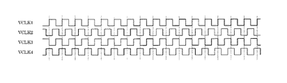
- H04N2201/04781—Controlling the phase of the signals
- H04N2201/04784—Controlling the phase of the signals using one or more clock signals selected from a number of clock signals of different phases
-
- H—ELECTRICITY
- H04—ELECTRIC COMMUNICATION TECHNIQUE
- H04N—PICTORIAL COMMUNICATION, e.g. TELEVISION
- H04N2201/00—Indexing scheme relating to scanning, transmission or reproduction of documents or the like, and to details thereof
- H04N2201/04—Scanning arrangements
- H04N2201/047—Detection, control or error compensation of scanning velocity or position
- H04N2201/04753—Control or error compensation of scanning position or velocity
- H04N2201/04794—Varying the control or compensation during the scan, e.g. using continuous feedback or from line to line
Landscapes
- Engineering & Computer Science (AREA)
- Physics & Mathematics (AREA)
- Multimedia (AREA)
- General Engineering & Computer Science (AREA)
- General Physics & Mathematics (AREA)
- Theoretical Computer Science (AREA)
- Optics & Photonics (AREA)
- Signal Processing (AREA)
- Facsimile Scanning Arrangements (AREA)
- Laser Beam Printer (AREA)
- Mechanical Optical Scanning Systems (AREA)
- Facsimile Heads (AREA)
- Facsimile Image Signal Circuits (AREA)
Description
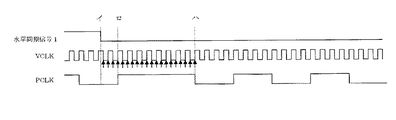
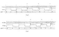
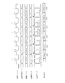
変調データ割当回路133にて、画素制御データに基づき、第2変調データの各bitを出力である変調データの各bitに割り当て、変調データとして出力する。同時に、位相データ生成回路134から、画素制御データに基づいて位相データを出力する。図9では、簡単化のため画素クロックPCLKの信号線を省略したが、変調データと位相データは画素クロックに同期して出力される。
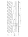
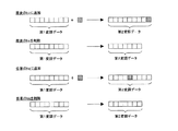
図11(イ)のクロックでは、画素制御データは“0”なので、画像データDATA(m−1)に対応した第2変調データとしてDPM(m−1)[31:0]の32bitのデータが得られ、変調データD0〜D31それぞれにDPM(m−1)[0]〜DPM(m−1)[31]をロのクロックで出力する。図11(ロ)のクロックでは、画素制御データは“1”なので、画像データDATA(m)に対応した第2変調データとしてDPM(m)[32:0]の33bitのデータが得られる。そして、変調データD0〜D31それぞれにDPM(m)[0]〜DPM(m)[31]をハのクロックで出力し、DPM(m)[32]はニのクロックにおける変調データD0に出力する。図11(ハ)のクロックでは、画素制御データは“0”なので、画像データDATA(m+1)に対応した第2変調データとしてDPM(m+1)[31:0]の32bitのデータが得られる。そして、ここでは変調データD0には先程のDPM(m)[32]を、D1〜D31にはDPM(m+1)[0]〜DPM(m+1)[30]をニのクロックで出力する。DPM(m+1)[31]は、ホのクロックにおける変調データD0に出力する。図11(ニ)のクロックでは、画素制御データは“1”なので、画像データDATA(m+2)に対応した第2変調データとしてDPM(m+2)[32:0]の33bitのデータが得られる。そして、この時位相データとして“1”をホのクロックで出力する。ホのクロックは位相データが”1”であることから位相シフトがおこり、そのクロックは長くなる。そのため変調データ幅も長くなりD0〜D33となる。よってD0には先程のDPM(m+1)[31]を、D1〜D33にDPM(m+2)[0]〜DPM(m+2)[32]をホのクロックで出力する。図11(ホ)のクロックでは、画素制御データは“0”なので、画像データDATA(m+3)に対応した第2変調データとしてDPM(m+3)[31:0]の32bitのデータが得られ、変調データD0〜D31それぞれにDPM(m+3)[0]〜DPM(m+3)[31]をヘのクロックで出力する。
図12(イ)のクロックでは、画素制御データは“0”なので、画像データDATA(m−1)に対応した第2変調データとしてDPM(m−1)[31:0]の32bitのデータが得られ、変調データD0〜D31それぞれにDPM(m−1)[0]〜DPM(m−1)[31]をロのクロックで出力する。図12(ロ)のクロックでは、画素制御データは“−1”なので画像データDATA(m)に対応した第2変調データとしてDPM(m)[30:0]の31bitのデータが得られる。そして、変調データD0〜D30それぞれにDPM(m)[0]〜DPM(m)[30]を、D31には次の画像データDATA(m+1)に対応する変調データDPM(m+1)[0]をハのクロックで出力する。図12(ハ)のクロックでは、画素制御データは“0”なので、画像データDATA(m+1)に対応した第2変調データとしてDPM(m+1)[31:0]の32bitのデータが得られる。そして、ここではDPM(m+1)[0]は一つ前の変調データD31に出力しているので、D0〜D30にDPM(m+1)[1]〜DPM(m+1)[31]を、D31には次の画像データDATA(m+2)に対応する変調データDPM(m+2)[0]をニのクロックで出力する。図12(ニ)のクロックでは、画素制御データは“−1”なので、画像データDATA(m+2)に対応した第2変調データとしてDPM(m+2)[30:0]の31bitのデータが得られる。そして、この時位相データとして“−1”をホのクロックで出力する。ホのクロックは位相データが“−1”であることから位相シフトがおこりそのクロックは短くなる。そのため変調データ幅も短くなりD0〜D29となる。DPM(m+2)[0]は一つ前の変調データD31に出力しているので、D0〜D29にはDPM(m+2)[1]〜DPM(m+2)[30]をホのクロックで出力する。図12(ホ)のクロックでは、画素制御データは“0”なので、画像データDATA(m+3)に対応した第2変調データとしてDPM(m+3)[31:0]の32bitのデータが得られ、変調データD0〜D31それぞれにDPM(m+3)[0]〜DPM(m+3)[31]をヘのクロックで出力する。
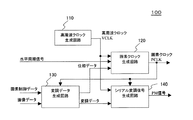
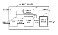
110 高周波クロック生成部
120 画素クロック生成部
130 変調データ生成部
140 レーザ駆動信号生成部(シリアル変調信号生成部)
200 レーザ駆動部
300 走査光学系
400 ドット位置ずれ検出・制御部
500 画像処理部
Claims (12)
- 高周波クロックを生成する高周波クロック生成手段と、
画素の長さを指示する画素制御データに基づいて画素クロックの位相シフト量を指示する位相データを生成するとともに、画像データに対応した所望のビットパターンを表す変調データを生成し、前記画素制御データに基づいて前記変調データの長さを変化させる変調データ生成手段と、
前記高周波クロックと前記位相データと水平同期信号とに基づいて画素クロックを生成する画素クロック生成手段と、
前記変調データを入力し、前記画素クロックと高周波クロックに基づいて、前記位相データで指示された画素クロックの位相シフト量に応じた長さのシリアルパルス列のパルス変調信号を出力するシリアル変調信号生成手段と、
を有することを特徴とする画素クロック及びパルス変調信号生成装置。 - 前記変調データ生成手段は、
前記位相データで指示される画素クロックの位相シフト量に応じて、前記画素制御データに基づいて長さが変化する前記変調データを構成する複数のデータを2つの連続する画素クロックに分けて出力することを特徴とする請求項1に記載の画素クロック及びパルス変調信号生成装置。 - 請求項1又は2記載の画素クロック及びパルス変調信号生成装置において、
前記変調データ生成手段は、前記画素制御データに基づいて、前記変調データの追加あるいは削除を行うことを特徴とする画素クロック及びパルス変調信号生成装置。 - 請求項3記載の画素クロック及びパルス変調信号生成装置において、
画素を長くする場合は前記変調データの最後にデータを追加することを特徴とする画素クロック及びパルス変調信号生成装置。 - 請求項3記載の画素クロック及びパルス変調信号生成装置において、
画素を短くする場合は前記変調データの最後のデータを削除することを特徴とする画素クロック及びパルス変調信号生成装置。 - 請求項3記載の画素クロック及びパルス変調信号生成装置において、
画素を長くする場合は前記変調データの任意の位置にデータを追加することを特徴とする画素クロック及びパルス変調信号生成装置。 - 請求項3記載の画素クロック及びパルス変調信号生成装置において、
画素を短くする場合は前記変調データの任意の位置のデータを削除することを特徴とする画素クロック及びパルス変調信号生成装置。 - 請求項6記載の画素クロック及びパルス変調信号生成装置において、
前記変調データにデータを追加する位置は前記変調データのパターンに依存することを特徴とする画素クロック及びパルス変調信号生成装置。 - 請求項7記載の画素クロック及びパルス変調信号生成装置において、
前記変調データのデータを削除する位置は前記変調データのパターンに依存することを特徴とする画素クロック及びパルス変調信号生成装置。 - 請求項4、6、8のいずれか1項に記載の画素クロック及びパルス変調信号生成装置において、
前記変調データに追加するデータは前記変調データパターンに依存することを特徴とする画素クロック及びパルス変調信号生成装置。 - 光源から出力される光束を、偏向器により走査方向に沿って被走査媒体上を走査させる光走査装置において、
請求項1乃至10のいずれか1項に記載の画素クロック及びパルス変調信号生成装置を有することを特徴とする光走査装置。 - 請求項11記載の光走査装置を露光手段として用いて画像形成することを特徴とする画像形成装置。
Priority Applications (3)
| Application Number | Priority Date | Filing Date | Title |
|---|---|---|---|
| JP2004001982A JP4341908B2 (ja) | 2004-01-07 | 2004-01-07 | 画素クロック及びパルス変調信号生成装置、光走査装置並びに画像形成装置 |
| US11/030,419 US7327379B2 (en) | 2004-01-07 | 2005-01-07 | Pixel clock and pulse-modulation-signal generating device, optical scanner, and image forming apparatus |
| US11/844,854 US7973817B2 (en) | 2004-01-07 | 2007-08-24 | Pixel clock and pulse-modulation-signal generating device, optical scanner, and image forming apparatus |
Applications Claiming Priority (1)
| Application Number | Priority Date | Filing Date | Title |
|---|---|---|---|
| JP2004001982A JP4341908B2 (ja) | 2004-01-07 | 2004-01-07 | 画素クロック及びパルス変調信号生成装置、光走査装置並びに画像形成装置 |
Publications (2)
| Publication Number | Publication Date |
|---|---|
| JP2005198006A JP2005198006A (ja) | 2005-07-21 |
| JP4341908B2 true JP4341908B2 (ja) | 2009-10-14 |
Family
ID=34709023
Family Applications (1)
| Application Number | Title | Priority Date | Filing Date |
|---|---|---|---|
| JP2004001982A Expired - Fee Related JP4341908B2 (ja) | 2004-01-07 | 2004-01-07 | 画素クロック及びパルス変調信号生成装置、光走査装置並びに画像形成装置 |
Country Status (2)
| Country | Link |
|---|---|
| US (2) | US7327379B2 (ja) |
| JP (1) | JP4341908B2 (ja) |
Families Citing this family (35)
| Publication number | Priority date | Publication date | Assignee | Title |
|---|---|---|---|---|
| JP4341908B2 (ja) * | 2004-01-07 | 2009-10-14 | 株式会社リコー | 画素クロック及びパルス変調信号生成装置、光走査装置並びに画像形成装置 |
| JP4777720B2 (ja) * | 2005-08-24 | 2011-09-21 | 株式会社リコー | 光書き込み装置、画像形成装置、光書き込み方法、コンピュータプログラム及び記録媒体 |
| JP2007286423A (ja) * | 2006-04-18 | 2007-11-01 | Brother Ind Ltd | 光走査装置及び画像表示装置並びに網膜走査型画像表示装置 |
| JP4790532B2 (ja) * | 2006-08-01 | 2011-10-12 | 株式会社リコー | 撮像装置及び無線通信相手検索方法 |
| JP4912071B2 (ja) * | 2006-08-04 | 2012-04-04 | 株式会社リコー | 光走査装置、光走査方法、画像形成装置、カラー画像形成装置、プログラム、記録媒体 |
| JP5001606B2 (ja) * | 2006-08-31 | 2012-08-15 | 川崎マイクロエレクトロニクス株式会社 | タイミング検出回路 |
| JP4863840B2 (ja) * | 2006-10-27 | 2012-01-25 | 株式会社リコー | 画素形成装置、光走査装置、光走査方法、画像形成装置、カラー画像形成装置 |
| JP5083867B2 (ja) * | 2007-03-02 | 2012-11-28 | 株式会社リコー | 光源駆動装置、光走査装置及び画像形成装置 |
| US7995251B2 (en) * | 2007-03-30 | 2011-08-09 | Ricoh Company, Limited | Optical scanning device, optical scanning method, and image forming apparatus |
| US7760223B2 (en) * | 2007-05-14 | 2010-07-20 | Ricoh Company, Ltd. | Optical scan apparatus and image formation apparatus |
| JP4953918B2 (ja) * | 2007-05-23 | 2012-06-13 | 株式会社リコー | 光源駆動装置、光走査装置及び画像形成装置 |
| JP5354891B2 (ja) | 2007-11-22 | 2013-11-27 | キヤノン株式会社 | 画像形成装置 |
| JP2009157014A (ja) * | 2007-12-26 | 2009-07-16 | Ricoh Co Ltd | 光走査装置及び画像形成装置 |
| JP5194802B2 (ja) * | 2008-01-07 | 2013-05-08 | 株式会社リコー | 光源駆動装置、光走査装置及び画像形成装置 |
| JP5006810B2 (ja) * | 2008-02-06 | 2012-08-22 | 株式会社リコー | 光走査装置及び画像形成装置 |
| JP2009196226A (ja) | 2008-02-22 | 2009-09-03 | Ricoh Co Ltd | パルス変調信号生成装置、光源装置、光走査装置及び画像形成装置 |
| JP2009244843A (ja) * | 2008-03-14 | 2009-10-22 | Ricoh Co Ltd | 光走査装置およびカラー画像形成装置 |
| JP5036634B2 (ja) * | 2008-06-10 | 2012-09-26 | 株式会社リコー | 光源装置、光走査装置及び画像形成装置 |
| US8237760B2 (en) * | 2008-08-19 | 2012-08-07 | Ricoh Company, Ltd. | Light-source driving device, optical scanning device, and counting method |
| JP5402072B2 (ja) * | 2009-02-23 | 2014-01-29 | 株式会社リコー | 光源駆動装置、光走査装置及び画像形成装置 |
| JP5391873B2 (ja) * | 2009-06-30 | 2014-01-15 | コニカミノルタ株式会社 | 画像形成装置 |
| JP5805364B2 (ja) * | 2009-07-09 | 2015-11-04 | 株式会社リコー | 光源駆動装置、光走査装置及び画像形成装置 |
| JP2011066089A (ja) | 2009-09-15 | 2011-03-31 | Ricoh Co Ltd | 半導体レーザ制御装置及び画像形成装置 |
| JP5544887B2 (ja) | 2010-01-12 | 2014-07-09 | 株式会社リコー | 光走査装置及び画像形成装置 |
| JP5471569B2 (ja) * | 2010-02-18 | 2014-04-16 | 株式会社リコー | レーザ駆動装置、光走査装置、画像形成装置及びレーザ駆動方法 |
| JP2011258796A (ja) | 2010-06-10 | 2011-12-22 | Ricoh Co Ltd | レーザ駆動装置、光走査装置並びに画像形成装置 |
| JP5836684B2 (ja) * | 2011-07-25 | 2015-12-24 | キヤノン株式会社 | 画像形成装置 |
| US8654168B2 (en) | 2011-08-03 | 2014-02-18 | Ricoh Company, Ltd. | Optical scanning device, image forming apparatus, and optical scanning device designing method |
| JP6120655B2 (ja) | 2013-04-18 | 2017-04-26 | キヤノン株式会社 | 画像形成装置 |
| JP6172506B2 (ja) | 2013-05-02 | 2017-08-02 | 株式会社リコー | 画像形成装置及び画像形成方法 |
| JP6167654B2 (ja) | 2013-05-09 | 2017-07-26 | 株式会社リコー | 画像形成装置、画像形成方法および印刷物の製造方法 |
| JP6171547B2 (ja) | 2013-05-10 | 2017-08-02 | 株式会社リコー | 画像形成装置、画像形成方法および印刷物の製造方法 |
| JP6127712B2 (ja) | 2013-05-21 | 2017-05-17 | 株式会社リコー | 光源駆動回路、光走査装置及び画像形成装置 |
| JP6230466B2 (ja) * | 2014-03-31 | 2017-11-15 | キヤノン株式会社 | 画像形成装置 |
| JP6596814B2 (ja) | 2014-11-25 | 2019-10-30 | 株式会社リコー | 画像形成装置 |
Family Cites Families (34)
| Publication number | Priority date | Publication date | Assignee | Title |
|---|---|---|---|---|
| US5117243A (en) * | 1990-04-06 | 1992-05-26 | S&R Tech Development, Inc. | Scanner with electronic non-linearity compensation and method of processing image data |
| JP3212200B2 (ja) * | 1992-11-27 | 2001-09-25 | 東芝テック株式会社 | 光走査装置 |
| JP3231610B2 (ja) * | 1995-12-22 | 2001-11-26 | 富士通株式会社 | カラー画像形成装置 |
| JPH1067141A (ja) | 1996-06-19 | 1998-03-10 | Ricoh Co Ltd | 半導体レーザ制御装置 |
| US6091891A (en) * | 1997-05-09 | 2000-07-18 | Lexmark International, Inc. | Method and apparatus for calibrating delay lines to create gray levels in continuous tone printing |
| JPH11167081A (ja) | 1997-09-30 | 1999-06-22 | Eastman Kodak Co | 周波数可変画素クロック |
| US6178031B1 (en) | 1999-12-20 | 2001-01-23 | Xerox Corporation | Raster output scanning system having scan line non-linearity compensation means |
| AU2001277694A1 (en) * | 2000-07-28 | 2002-02-13 | Nichia Corporation | Display and display drive circuit or display drive method |
| JP4154856B2 (ja) * | 2000-12-28 | 2008-09-24 | コニカミノルタホールディングス株式会社 | クロック発生回路および画像形成装置 |
| JP3515087B2 (ja) | 2001-09-28 | 2004-04-05 | 株式会社リコー | パルス変調信号生成回路、半導体レーザ変調装置、光学走査装置及び画像形成装置 |
| EP1241869B1 (en) * | 2001-03-14 | 2010-08-11 | Ricoh Company, Ltd. | Light-emission modulation having effective scheme of creating gray scale on image |
| US6791596B2 (en) * | 2001-06-28 | 2004-09-14 | Ricoh Company, Ltd. | Method and apparatus for image forming capable of effectively generating pixel clock pulses |
| JP2003015068A (ja) | 2001-07-02 | 2003-01-15 | Ricoh Co Ltd | 画像形成装置および画素クロック生成回路 |
| JP3512397B2 (ja) | 2001-09-25 | 2004-03-29 | 株式会社リコー | 画素クロック生成回路及び画像形成装置 |
| JP2003034051A (ja) | 2001-07-25 | 2003-02-04 | Ricoh Co Ltd | 画素クロック生成装置、光書き込み装置および画像形成装置 |
| JP2003279873A (ja) | 2002-03-20 | 2003-10-02 | Ricoh Co Ltd | 光走査装置及び画像形成装置 |
| US7271824B2 (en) * | 2001-09-28 | 2007-09-18 | Ricoh Company, Ltd. | Pixel clock generating apparatus, optical writing apparatus using a pixel clock, imaging apparatus, and method for generating pixel clocks |
| JP4323120B2 (ja) | 2001-09-28 | 2009-09-02 | 株式会社リコー | 画素クロック生成方法、画素クロック生成装置及び画像形成装置 |
| US7256815B2 (en) | 2001-12-20 | 2007-08-14 | Ricoh Company, Ltd. | Image forming method, image forming apparatus, optical scan device, and image forming apparatus using the same |
| JP4007807B2 (ja) | 2001-12-20 | 2007-11-14 | 株式会社リコー | 光走査装置およびこれを用いた画像形成装置 |
| JP2003320702A (ja) | 2002-04-30 | 2003-11-11 | Ricoh Co Ltd | 画像形成方法および画像形成装置 |
| JP3600228B2 (ja) * | 2002-03-01 | 2004-12-15 | 株式会社リコー | 光走査装置および画像形成装置 |
| JP2003300341A (ja) | 2002-04-10 | 2003-10-21 | Ricoh Co Ltd | 画素クロック生成装置、レーザ走査装置、及び画像形成装置 |
| JP2003322810A (ja) | 2002-05-01 | 2003-11-14 | Ricoh Co Ltd | 画素クロック生成装置、光走査装置、画像形成装置、及び主走査ドット位置ずれ補正方法 |
| JP4593884B2 (ja) * | 2002-05-10 | 2010-12-08 | キヤノン株式会社 | レーザ走査制御装置 |
| JP2003344790A (ja) | 2002-05-27 | 2003-12-03 | Ricoh Co Ltd | 画素クロック生成装置、レーザ走査装置、及び画像形成装置 |
| US7283151B2 (en) | 2002-05-27 | 2007-10-16 | Ricoh Company, Ltd. | Pixel clock generation device causing state transition of pixel clock according to detected state transition and phase data indicating phase shift amount |
| JP2004351908A (ja) * | 2002-07-31 | 2004-12-16 | Canon Inc | 画像形成装置およびその主走査倍率補正方法 |
| US6933957B2 (en) | 2002-09-24 | 2005-08-23 | Ricoh Company, Ltd. | Pixel clock generation apparatus, pixel clock generation method, and image forming apparatus capable of correcting main scan dot position shift with a high degree of accuracy |
| JP4308495B2 (ja) | 2002-09-24 | 2009-08-05 | 株式会社リコー | 光走査装置及び画像形成装置 |
| JP4462917B2 (ja) * | 2003-01-23 | 2010-05-12 | 株式会社リコー | 光ビーム書込装置、画像形成装置、画像補正方法 |
| JP4165746B2 (ja) | 2003-02-07 | 2008-10-15 | 株式会社リコー | 画素クロック生成回路及び画像形成装置 |
| JP4227817B2 (ja) * | 2003-02-28 | 2009-02-18 | 株式会社リコー | 画像形成装置 |
| JP4341908B2 (ja) * | 2004-01-07 | 2009-10-14 | 株式会社リコー | 画素クロック及びパルス変調信号生成装置、光走査装置並びに画像形成装置 |
-
2004
- 2004-01-07 JP JP2004001982A patent/JP4341908B2/ja not_active Expired - Fee Related
-
2005
- 2005-01-07 US US11/030,419 patent/US7327379B2/en not_active Expired - Fee Related
-
2007
- 2007-08-24 US US11/844,854 patent/US7973817B2/en not_active Expired - Fee Related
Also Published As
| Publication number | Publication date |
|---|---|
| JP2005198006A (ja) | 2005-07-21 |
| US20050146596A1 (en) | 2005-07-07 |
| US20080012933A1 (en) | 2008-01-17 |
| US7973817B2 (en) | 2011-07-05 |
| US7327379B2 (en) | 2008-02-05 |
Similar Documents
| Publication | Publication Date | Title |
|---|---|---|
| JP4341908B2 (ja) | 画素クロック及びパルス変調信号生成装置、光走査装置並びに画像形成装置 | |
| JP4336177B2 (ja) | 画素クロック生成装置、光走査装置及び画像形成装置 | |
| JP5078836B2 (ja) | 光走査装置および画像形成装置 | |
| JP2007038477A (ja) | 画素クロック及びパルス変調信号生成装置、光走査装置及び画像形成装置 | |
| JP2000180747A (ja) | 光学走査装置 | |
| JP3078557B2 (ja) | ディジタルプリンタ | |
| JPH11198435A (ja) | 画像形成装置 | |
| US6806894B2 (en) | Image forming apparatus and main scanning scale correcting method therefor | |
| US7652682B2 (en) | Image forming apparatus | |
| US20080018727A1 (en) | Optical beam scanning apparatus, optical beam scanning method, optical beam scanning program, image forming apparatus, image forming method, image forming program | |
| JP5276351B2 (ja) | 画像形成装置 | |
| JPH1155472A (ja) | 多色画像形成装置 | |
| US7433074B2 (en) | Image forming apparatus and image forming method | |
| JP4367840B2 (ja) | 画素クロック生成装置、光走査装置及び画像形成装置 | |
| JP2007090758A (ja) | 画像形成装置 | |
| US7804514B2 (en) | Light beam scanning apparatus and image forming apparatus | |
| JP4313132B2 (ja) | 画素クロック生成回路、画素クロック及びパルス変調信号生成回路、光走査装置および画像形成装置 | |
| JP2009196226A (ja) | パルス変調信号生成装置、光源装置、光走査装置及び画像形成装置 | |
| JP4134999B2 (ja) | 発光タイミング調整方法、レーザ走査装置及び画像形成装置 | |
| JP2004354626A (ja) | 画像形成装置及び該装置における水平同期信号発生方法 | |
| JP2003121770A (ja) | 画像形成装置 | |
| JP2006175646A (ja) | 画像形成システム及び画像形成方法 | |
| US7436424B2 (en) | Light beam scanning apparatus and image forming apparatus with parallel modulating and driving channels | |
| JP2004286862A (ja) | 光ビーム走査回路、光ビーム走査装置、および画像形成装置 | |
| JP2008225064A (ja) | 画素クロック生成装置および光走査装置および画像形成装置 |
Legal Events
| Date | Code | Title | Description |
|---|---|---|---|
| A621 | Written request for application examination |
Free format text: JAPANESE INTERMEDIATE CODE: A621 Effective date: 20060825 |
|
| A977 | Report on retrieval |
Free format text: JAPANESE INTERMEDIATE CODE: A971007 Effective date: 20090119 |
|
| A131 | Notification of reasons for refusal |
Free format text: JAPANESE INTERMEDIATE CODE: A131 Effective date: 20090128 |
|
| A521 | Written amendment |
Free format text: JAPANESE INTERMEDIATE CODE: A523 Effective date: 20090326 |
|
| TRDD | Decision of grant or rejection written | ||
| A01 | Written decision to grant a patent or to grant a registration (utility model) |
Free format text: JAPANESE INTERMEDIATE CODE: A01 Effective date: 20090701 |
|
| A01 | Written decision to grant a patent or to grant a registration (utility model) |
Free format text: JAPANESE INTERMEDIATE CODE: A01 |
|
| A61 | First payment of annual fees (during grant procedure) |
Free format text: JAPANESE INTERMEDIATE CODE: A61 Effective date: 20090703 |
|
| FPAY | Renewal fee payment (event date is renewal date of database) |
Free format text: PAYMENT UNTIL: 20120717 Year of fee payment: 3 |
|
| FPAY | Renewal fee payment (event date is renewal date of database) |
Free format text: PAYMENT UNTIL: 20120717 Year of fee payment: 3 |
|
| FPAY | Renewal fee payment (event date is renewal date of database) |
Free format text: PAYMENT UNTIL: 20120717 Year of fee payment: 3 |
|
| FPAY | Renewal fee payment (event date is renewal date of database) |
Free format text: PAYMENT UNTIL: 20130717 Year of fee payment: 4 |
|
| LAPS | Cancellation because of no payment of annual fees |