JP2010062269A - ウェーハ積層体の製造方法、ウェーハ積層体製造装置、ウェーハ積層体、支持層剥離方法、及びウェーハの製造方法 - Google Patents
ウェーハ積層体の製造方法、ウェーハ積層体製造装置、ウェーハ積層体、支持層剥離方法、及びウェーハの製造方法 Download PDFInfo
- Publication number
- JP2010062269A JP2010062269A JP2008225231A JP2008225231A JP2010062269A JP 2010062269 A JP2010062269 A JP 2010062269A JP 2008225231 A JP2008225231 A JP 2008225231A JP 2008225231 A JP2008225231 A JP 2008225231A JP 2010062269 A JP2010062269 A JP 2010062269A
- Authority
- JP
- Japan
- Prior art keywords
- wafer
- support layer
- adhesive
- layer
- manufacturing
- Prior art date
- Legal status (The legal status is an assumption and is not a legal conclusion. Google has not performed a legal analysis and makes no representation as to the accuracy of the status listed.)
- Pending
Links
Images


Classifications
-
- H—ELECTRICITY
- H01—ELECTRIC ELEMENTS
- H01L—SEMICONDUCTOR DEVICES NOT COVERED BY CLASS H10
- H01L21/00—Processes or apparatus adapted for the manufacture or treatment of semiconductor or solid state devices or of parts thereof
- H01L21/67—Apparatus specially adapted for handling semiconductor or electric solid state devices during manufacture or treatment thereof; Apparatus specially adapted for handling wafers during manufacture or treatment of semiconductor or electric solid state devices or components ; Apparatus not specifically provided for elsewhere
- H01L21/68—Apparatus specially adapted for handling semiconductor or electric solid state devices during manufacture or treatment thereof; Apparatus specially adapted for handling wafers during manufacture or treatment of semiconductor or electric solid state devices or components ; Apparatus not specifically provided for elsewhere for positioning, orientation or alignment
-
- H—ELECTRICITY
- H01—ELECTRIC ELEMENTS
- H01L—SEMICONDUCTOR DEVICES NOT COVERED BY CLASS H10
- H01L21/00—Processes or apparatus adapted for the manufacture or treatment of semiconductor or solid state devices or of parts thereof
- H01L21/67—Apparatus specially adapted for handling semiconductor or electric solid state devices during manufacture or treatment thereof; Apparatus specially adapted for handling wafers during manufacture or treatment of semiconductor or electric solid state devices or components ; Apparatus not specifically provided for elsewhere
- H01L21/683—Apparatus specially adapted for handling semiconductor or electric solid state devices during manufacture or treatment thereof; Apparatus specially adapted for handling wafers during manufacture or treatment of semiconductor or electric solid state devices or components ; Apparatus not specifically provided for elsewhere for supporting or gripping
- H01L21/6835—Apparatus specially adapted for handling semiconductor or electric solid state devices during manufacture or treatment thereof; Apparatus specially adapted for handling wafers during manufacture or treatment of semiconductor or electric solid state devices or components ; Apparatus not specifically provided for elsewhere for supporting or gripping using temporarily an auxiliary support
-
- H—ELECTRICITY
- H01—ELECTRIC ELEMENTS
- H01L—SEMICONDUCTOR DEVICES NOT COVERED BY CLASS H10
- H01L21/00—Processes or apparatus adapted for the manufacture or treatment of semiconductor or solid state devices or of parts thereof
- H01L21/02—Manufacture or treatment of semiconductor devices or of parts thereof
- H01L21/04—Manufacture or treatment of semiconductor devices or of parts thereof the devices having at least one potential-jump barrier or surface barrier, e.g. PN junction, depletion layer or carrier concentration layer
- H01L21/18—Manufacture or treatment of semiconductor devices or of parts thereof the devices having at least one potential-jump barrier or surface barrier, e.g. PN junction, depletion layer or carrier concentration layer the devices having semiconductor bodies comprising elements of Group IV of the Periodic System or AIIIBV compounds with or without impurities, e.g. doping materials
- H01L21/30—Treatment of semiconductor bodies using processes or apparatus not provided for in groups H01L21/20 - H01L21/26
- H01L21/302—Treatment of semiconductor bodies using processes or apparatus not provided for in groups H01L21/20 - H01L21/26 to change their surface-physical characteristics or shape, e.g. etching, polishing, cutting
- H01L21/304—Mechanical treatment, e.g. grinding, polishing, cutting
-
- H—ELECTRICITY
- H01—ELECTRIC ELEMENTS
- H01L—SEMICONDUCTOR DEVICES NOT COVERED BY CLASS H10
- H01L21/00—Processes or apparatus adapted for the manufacture or treatment of semiconductor or solid state devices or of parts thereof
- H01L21/67—Apparatus specially adapted for handling semiconductor or electric solid state devices during manufacture or treatment thereof; Apparatus specially adapted for handling wafers during manufacture or treatment of semiconductor or electric solid state devices or components ; Apparatus not specifically provided for elsewhere
- H01L21/683—Apparatus specially adapted for handling semiconductor or electric solid state devices during manufacture or treatment thereof; Apparatus specially adapted for handling wafers during manufacture or treatment of semiconductor or electric solid state devices or components ; Apparatus not specifically provided for elsewhere for supporting or gripping
- H01L21/6835—Apparatus specially adapted for handling semiconductor or electric solid state devices during manufacture or treatment thereof; Apparatus specially adapted for handling wafers during manufacture or treatment of semiconductor or electric solid state devices or components ; Apparatus not specifically provided for elsewhere for supporting or gripping using temporarily an auxiliary support
- H01L21/6836—Wafer tapes, e.g. grinding or dicing support tapes
-
- H—ELECTRICITY
- H01—ELECTRIC ELEMENTS
- H01L—SEMICONDUCTOR DEVICES NOT COVERED BY CLASS H10
- H01L2221/00—Processes or apparatus adapted for the manufacture or treatment of semiconductor or solid state devices or of parts thereof covered by H01L21/00
- H01L2221/67—Apparatus for handling semiconductor or electric solid state devices during manufacture or treatment thereof; Apparatus for handling wafers during manufacture or treatment of semiconductor or electric solid state devices or components; Apparatus not specifically provided for elsewhere
- H01L2221/683—Apparatus for handling semiconductor or electric solid state devices during manufacture or treatment thereof; Apparatus for handling wafers during manufacture or treatment of semiconductor or electric solid state devices or components; Apparatus not specifically provided for elsewhere for supporting or gripping
- H01L2221/68304—Apparatus for handling semiconductor or electric solid state devices during manufacture or treatment thereof; Apparatus for handling wafers during manufacture or treatment of semiconductor or electric solid state devices or components; Apparatus not specifically provided for elsewhere for supporting or gripping using temporarily an auxiliary support
- H01L2221/68327—Apparatus for handling semiconductor or electric solid state devices during manufacture or treatment thereof; Apparatus for handling wafers during manufacture or treatment of semiconductor or electric solid state devices or components; Apparatus not specifically provided for elsewhere for supporting or gripping using temporarily an auxiliary support used during dicing or grinding
-
- H—ELECTRICITY
- H01—ELECTRIC ELEMENTS
- H01L—SEMICONDUCTOR DEVICES NOT COVERED BY CLASS H10
- H01L2221/00—Processes or apparatus adapted for the manufacture or treatment of semiconductor or solid state devices or of parts thereof covered by H01L21/00
- H01L2221/67—Apparatus for handling semiconductor or electric solid state devices during manufacture or treatment thereof; Apparatus for handling wafers during manufacture or treatment of semiconductor or electric solid state devices or components; Apparatus not specifically provided for elsewhere
- H01L2221/683—Apparatus for handling semiconductor or electric solid state devices during manufacture or treatment thereof; Apparatus for handling wafers during manufacture or treatment of semiconductor or electric solid state devices or components; Apparatus not specifically provided for elsewhere for supporting or gripping
- H01L2221/68304—Apparatus for handling semiconductor or electric solid state devices during manufacture or treatment thereof; Apparatus for handling wafers during manufacture or treatment of semiconductor or electric solid state devices or components; Apparatus not specifically provided for elsewhere for supporting or gripping using temporarily an auxiliary support
- H01L2221/6834—Apparatus for handling semiconductor or electric solid state devices during manufacture or treatment thereof; Apparatus for handling wafers during manufacture or treatment of semiconductor or electric solid state devices or components; Apparatus not specifically provided for elsewhere for supporting or gripping using temporarily an auxiliary support used to protect an active side of a device or wafer
-
- Y—GENERAL TAGGING OF NEW TECHNOLOGICAL DEVELOPMENTS; GENERAL TAGGING OF CROSS-SECTIONAL TECHNOLOGIES SPANNING OVER SEVERAL SECTIONS OF THE IPC; TECHNICAL SUBJECTS COVERED BY FORMER USPC CROSS-REFERENCE ART COLLECTIONS [XRACs] AND DIGESTS
- Y10—TECHNICAL SUBJECTS COVERED BY FORMER USPC
- Y10T—TECHNICAL SUBJECTS COVERED BY FORMER US CLASSIFICATION
- Y10T156/00—Adhesive bonding and miscellaneous chemical manufacture
- Y10T156/11—Methods of delaminating, per se; i.e., separating at bonding face
Landscapes
- Engineering & Computer Science (AREA)
- Physics & Mathematics (AREA)
- Condensed Matter Physics & Semiconductors (AREA)
- General Physics & Mathematics (AREA)
- Manufacturing & Machinery (AREA)
- Computer Hardware Design (AREA)
- Microelectronics & Electronic Packaging (AREA)
- Power Engineering (AREA)
- Mechanical Treatment Of Semiconductor (AREA)
- Container, Conveyance, Adherence, Positioning, Of Wafer (AREA)
Abstract
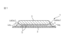
【解決手段】ウェーハ積層体1の製造方法であって、ウェーハ2を上側に位置するウェーハ吸着台で吸着し、支持層3を下側に位置する支持層吸着台で吸着し、ウェーハ2と支持層3とを上下方向に対向させて配置する工程と、ウェーハ2に対する支持層3の対向面に、接着層4を形成するために液状の接着性樹脂を塗布する工程と、ウェーハ2及び支持層3の平行度を維持したまま両者を接近させ、接着性樹脂が介在している状態で加圧して、接着性樹脂を広げることで、ウェーハ2と支持層3との間を接着性樹脂で塞ぎ、かつ、ウェーハ2の側壁外周に樹脂突出部4aを形成する工程と、を含む。
【選択図】図1
Description
また、裏面研削後に支持層及び接着層を容易に剥離することができるウェーハ積層体の製造方法、ウェーハ積層体製造装置、ウェーハ積層体、支持層剥離方法、及びウェーハの製造方法を提供することを目的とする。
この製造方法によれば、裏面研削時のウェーハ割れやウェーハのエッジ部におけるチッピングを防止することができ、ウェーハの裏面研削特性に優れるウェーハ積層体を作製することができる。また、接着層によりウェーハ表面の凹凸を吸収することができるから、裏面研削時におけるウェーハ割れを防止することができる。
この製造装置によれば、ウェーハの裏面研削特性に優れるウェーハ積層体を作製することができる。
このウェーハ積層体によれば、接着層により、ウェーハ表面の凹凸を吸収でき、裏面研削時のウェーハ割れを防止することできる。
この支持層剥離方法によれば、ウェーハの裏面研削後は、複雑な装置を用いることなく、ウェーハに剥離不良を生じさせることなく、ウェーハから支持層と共に接着層を剥離することができる。
このウェーハの製造方法によれば、研削時におけるウェーハの損傷や、ピーリング時におけるウェーハの損傷を防止でき、中間製品としてのウェーハ積層体から最終製品としての薄いウェーハを得ることができる。
1)裏面研磨時(研削時)に接着層4によるずれ、たわみを生じさせないため、23℃でのJIS K 6251−1993で規定するダンベル状3号形を使用して500mm/分で引っ張ったときの破断伸度は50%以下、更に好ましくは30%以下であることが好ましく、且つ、
2)樹脂フィルム3・接着層4の剥離時に凹凸面への接着層4の機械的な投錨力(アンカー効果)による剥離不良を低減するため、同破断伸度は5%以下であることが好ましい。
3)また、フィルム3・接着層4の剥離時に軽微な剥離力で剥がせ、かつ接着層4の破断を生じさせないため、接着剤は適度な強度と柔軟性をあわせもつ必要がある。具体的には23℃における硬化後の接着剤の引張弾性率(レオメトリックス社、RSAII型 動的粘弾性装置を使用し、周波数10ヘルツで測定)が1.0〜9.0×10⁸Paであることが好ましい。引張弾性率は弾性限度の度合い示すものであり、接着剤の弾性を適切に評価するものとして用いられている。良好な剥離性能を示す接着剤の例としては、住友3M株式会社から販売されているLC3000シリーズを挙げることができる。弾性率が低すぎると接着剤が粘着剤を示し、良好な剥離を期待できず、また剥離時に接着剤の破断を伴う恐れがあるからである。弾性率が高すぎると柔軟性が失われ、同様に接着剤が部分的に被接着面に残留しやすくなるからである。
2 ウェーハ
3 樹脂フィルム
4 接着剤
10,10A 製造装置
18 上部吸着台(ウェーハ吸着台)
26 下部吸着台(フィルム吸着台)
33 照射源
Claims (13)
- ウェーハ積層体の製造方法であって、
前記ウェーハ積層体が、
a)ウェーハと、
b)該ウェーハを支持する支持層と、
c)前記ウェーハと前記支持層とを接着する接着層と、
d)前記ウェーハの側壁外周に形成された樹脂突出部と、を備え、
(1)前記ウェーハを上側に位置するウェーハ吸着台で吸着し、前記支持層を下側に位置する支持層吸着台で吸着し、前記ウェーハと前記支持層とを上下方向に対向させて配置する工程と、
(2)前記ウェーハに対する前記支持層の対向面に、前記接着層を形成するために液状の接着性樹脂を塗布する工程と、
(3)前記ウェーハ及び前記支持層の平行度を維持したまま両者を接近させ、前記接着性樹脂が介在している状態で加圧して、前記接着性樹脂を広げることで、前記ウェーハと前記支持層との間を前記接着性樹脂で塞ぎ、かつ、前記ウェーハの側壁外周に前記樹脂突出部を形成する工程と、
(4)前記ウェーハ積層体が所定の厚みに達した時点で、前記接着性樹脂に外部から紫外線を供給することにより前記接着性樹脂を硬化させ、前記接着層を形成する工程と、
を含むウェーハ積層体の製造方法。 - 前記ウェーハ及び前記支持層との間を真空雰囲気とし、前記接着性樹脂が介在している状態で加圧して前記接着性樹脂を広げることで、前記ウェーハと前記支持層との間を前記接着性樹脂で塞ぎ、かつ、前記ウェーハの側壁外周に前記樹脂突出部を形成する、請求項1記載のウェーハ積層体の製造方法。
- 吸着面が凹凸面である前記支持層吸着台と前記支持層との間から気泡を排出しながら、前記支持層を前記支持層吸着台で吸着する、請求項1又は2に記載のウェーハ積層体の製造方法。
- 前記ウェーハを前記ウェーハ吸着台で吸着する前に、前記接着層と略同質の接着性樹脂で、前記ウェーハの対向面を下地処理する、請求項1〜3の何れか1項に記載のウェーハ積層体の製造方法。
- 前記支持層が、室温23℃における曲げ弾性率が1000MPa以上、10000MPa以下で、厚みが30〜200μmの樹脂層である請求項1〜4の何れか1項に記載のウェーハ積層体の製造方法。
- 前記支持層が前記ウェーハの外径よりも大きい寸法であり、前記ウェーハと前記支持層との間からはみ出した前記接着性樹脂を受ける、請求項1〜5の何れか1項に記載のウェーハ積層体の製造方法。
- 前記接着層は、硬化前の液体状態における室温23℃での粘度が100cP以上、10000cP未満であり、紫外線照射によって固化する接着性樹脂層である、請求項1〜6の何れか1に記載のウェーハ積層体の製造方法。
- ウェーハを吸着するウェーハ吸着台、
該ウェーハ吸着台の下側で相対向して配置され、液状の接着性樹脂を介して前記ウェーハに貼着される支持層を真空吸着する支持層吸着台、及び
前記接着性樹脂を硬化するために、該接着性樹脂に紫外線を照射する紫外線照射源、を備える、ウェーハ積層体製造装置であって、
前記支持層吸着台は、前記紫外線を透過させ、かつ、前記支持層を吸着する凹凸形状を有する、ウェーハ積層体製造装置。 - 前記支持層吸着台が吸着面に凹凸を有するガラスである、請求項8に記載のウェーハ積層体製造装置。
- 請求項1〜7の何れか1項に記載のウェーハ積層体の製造方法により作製したウェーハ積層体。
- ウェーハと、
該ウェーハを支持している支持層と、
前記ウェーハと前記支持層とを接着している接着層と、
前記ウェーハの側壁外周に形成された樹脂突出部と、
を有したウェーハ積層体。 - 請求項10又は11記載のウェーハ積層体の裏面を研削して前記ウェーハを所定の厚みまで薄くした後、前記ウェーハ積層体から前記支持層を前記接着層と共に剥離する支持層剥離方法であって、
前記支持層をU字状に折り返したときに、前記ウェーハを曲げないようにして、前記支持層を前記接着層と共に前記ウェーハ積層体から剥離する、支持層剥離方法。 - 請求項10又は11記載のウェーハ積層体を用意することと、
前記ウェーハを所望の厚さまで研削することと、
研削後に、前記ウェーハ積層体から前記支持層を前記接着層と共に剥離することと、を含む、ウェーハの製造方法。
Priority Applications (7)
| Application Number | Priority Date | Filing Date | Title |
|---|---|---|---|
| JP2008225231A JP2010062269A (ja) | 2008-09-02 | 2008-09-02 | ウェーハ積層体の製造方法、ウェーハ積層体製造装置、ウェーハ積層体、支持層剥離方法、及びウェーハの製造方法 |
| KR1020117007212A KR20110074855A (ko) | 2008-09-02 | 2009-08-27 | 웨이퍼 적층체의 제조 방법, 웨이퍼 적층체의 제조 장치, 웨이퍼 적층체, 지지체의 박리 방법, 및 웨이퍼의 제조 방법 |
| US13/059,113 US20110151176A1 (en) | 2008-09-02 | 2009-08-27 | Method of manufacturing wafer laminated body, device of manufacturing wafer laminated body, wafer laminated body, method of peeling support body, and method of manufacturing wafer |
| CN2009801424501A CN102197470A (zh) | 2008-09-02 | 2009-08-27 | 制造晶片层合体的方法、制造晶片层合体的装置、晶片层合体、剥离支撑体的方法以及制造晶片的方法 |
| PCT/US2009/055142 WO2010027897A1 (en) | 2008-09-02 | 2009-08-27 | Method of manufacturing wafer laminated body, device of manufacturing wafer laminated body, wafer laminated body, method of peeling support body, and method of manufacturing wafer |
| EP09791982A EP2335278A1 (en) | 2008-09-02 | 2009-08-27 | Method of manufacturing wafer laminated body, device of manufacturing wafer laminated body, wafer laminated body, method of peeling support body, and method of manufacturing wafer |
| TW098129412A TW201017743A (en) | 2008-09-02 | 2009-09-01 | Method of manufacturing wafer laminated body, device of manufacturing wafer laminated body, wafer laminated body, method of peeling support body, and method of manufacturing wafer |
Applications Claiming Priority (1)
| Application Number | Priority Date | Filing Date | Title |
|---|---|---|---|
| JP2008225231A JP2010062269A (ja) | 2008-09-02 | 2008-09-02 | ウェーハ積層体の製造方法、ウェーハ積層体製造装置、ウェーハ積層体、支持層剥離方法、及びウェーハの製造方法 |
Publications (2)
| Publication Number | Publication Date |
|---|---|
| JP2010062269A true JP2010062269A (ja) | 2010-03-18 |
| JP2010062269A5 JP2010062269A5 (ja) | 2011-10-13 |
Family
ID=41213305
Family Applications (1)
| Application Number | Title | Priority Date | Filing Date |
|---|---|---|---|
| JP2008225231A Pending JP2010062269A (ja) | 2008-09-02 | 2008-09-02 | ウェーハ積層体の製造方法、ウェーハ積層体製造装置、ウェーハ積層体、支持層剥離方法、及びウェーハの製造方法 |
Country Status (7)
| Country | Link |
|---|---|
| US (1) | US20110151176A1 (ja) |
| EP (1) | EP2335278A1 (ja) |
| JP (1) | JP2010062269A (ja) |
| KR (1) | KR20110074855A (ja) |
| CN (1) | CN102197470A (ja) |
| TW (1) | TW201017743A (ja) |
| WO (1) | WO2010027897A1 (ja) |
Cited By (18)
| Publication number | Priority date | Publication date | Assignee | Title |
|---|---|---|---|---|
| JP2011009422A (ja) * | 2009-06-25 | 2011-01-13 | Hitachi Setsubi Eng Co Ltd | ダイシングテープ用の真空貼付機 |
| JP2011119578A (ja) * | 2009-12-07 | 2011-06-16 | Disco Abrasive Syst Ltd | 貼着装置 |
| JP2012222026A (ja) * | 2011-04-05 | 2012-11-12 | Disco Abrasive Syst Ltd | ウェーハの研削方法 |
| JP2013175647A (ja) * | 2012-02-27 | 2013-09-05 | Disco Abrasive Syst Ltd | 樹脂貼付装置 |
| JP2014078550A (ja) * | 2012-10-09 | 2014-05-01 | Disco Abrasive Syst Ltd | 樹脂貼着装置 |
| JP2014078655A (ja) * | 2012-10-12 | 2014-05-01 | Disco Abrasive Syst Ltd | 樹脂貼着装置 |
| JP2014212188A (ja) * | 2013-04-18 | 2014-11-13 | 株式会社ディスコ | 板状物の貼着方法 |
| WO2014188879A1 (ja) * | 2013-05-24 | 2014-11-27 | 富士電機株式会社 | 半導体装置の製造方法 |
| KR101506854B1 (ko) | 2013-12-27 | 2015-03-31 | 경기대학교 산학협력단 | Uv 마운팅 장치 |
| JP2015213111A (ja) * | 2014-05-01 | 2015-11-26 | スリーエム イノベイティブ プロパティズ カンパニー | シート貼付方法、シート貼付装置及びウエハ加工方法 |
| JP2017216275A (ja) * | 2016-05-30 | 2017-12-07 | 株式会社ディスコ | テープ貼着方法 |
| JP2018125323A (ja) * | 2017-01-30 | 2018-08-09 | 株式会社ディスコ | 保護部材形成装置 |
| KR20180129671A (ko) * | 2017-05-26 | 2018-12-05 | 도쿄엘렉트론가부시키가이샤 | 기판 처리 장치 및 기판 유지부의 제조 방법 |
| JP2019149451A (ja) * | 2018-02-27 | 2019-09-05 | 株式会社ディスコ | 板状物の加工方法 |
| JP2019220550A (ja) * | 2018-06-19 | 2019-12-26 | 株式会社ディスコ | ウエーハの加工方法 |
| JP2020188230A (ja) * | 2019-05-17 | 2020-11-19 | 株式会社ディスコ | 保護部材形成装置 |
| JP2020188058A (ja) * | 2019-05-10 | 2020-11-19 | 株式会社ディスコ | 保護部材形成装置 |
| JP7471746B2 (ja) | 2020-01-15 | 2024-04-22 | 株式会社ディスコ | チャックテーブル、及びチャックテーブルの製造方法 |
Families Citing this family (18)
| Publication number | Priority date | Publication date | Assignee | Title |
|---|---|---|---|---|
| JP5406257B2 (ja) * | 2011-09-07 | 2014-02-05 | 東京エレクトロン株式会社 | 接合方法、プログラム、コンピュータ記憶媒体及び接合システム |
| JP5421967B2 (ja) * | 2011-09-07 | 2014-02-19 | 東京エレクトロン株式会社 | 接合方法、プログラム、コンピュータ記憶媒体及び接合システム |
| JP2013107168A (ja) * | 2011-11-21 | 2013-06-06 | Toyo Quality One Corp | ガラス研磨方法及びこれに用いる積層シート |
| JP5631343B2 (ja) * | 2012-02-08 | 2014-11-26 | 東京応化工業株式会社 | 積層体の製造方法 |
| JP6021362B2 (ja) * | 2012-03-09 | 2016-11-09 | 株式会社ディスコ | 板状物の研削方法 |
| JP6061590B2 (ja) * | 2012-09-27 | 2017-01-18 | 株式会社ディスコ | 表面保護部材および加工方法 |
| JP6288935B2 (ja) * | 2013-04-18 | 2018-03-07 | 株式会社ディスコ | シート |
| KR20150011072A (ko) | 2013-07-22 | 2015-01-30 | 삼성전자주식회사 | 임시 접착제 조성물 및 이를 이용한 반도체 소자의 제조 방법 |
| KR20150042362A (ko) * | 2013-10-10 | 2015-04-21 | 삼성전자주식회사 | 발광다이오드 패키지 및 그 제조방법 |
| JP6393127B2 (ja) * | 2014-09-10 | 2018-09-19 | 丸石産業株式会社 | 保持パッド |
| CN104409383B (zh) * | 2014-10-20 | 2017-08-01 | 上海技美电子科技有限公司 | 晶圆转移装置 |
| US9514772B2 (en) * | 2015-03-20 | 2016-12-06 | Tdk Corporation | Magnetic head device having suspension and spacer |
| CN105711224B (zh) * | 2016-03-25 | 2017-11-24 | 湖南新中合光电科技股份有限公司 | 一种光分路器晶圆贴片系统 |
| JP7108492B2 (ja) * | 2018-08-06 | 2022-07-28 | 株式会社ディスコ | 保護部材形成装置 |
| WO2020175364A1 (ja) * | 2019-02-26 | 2020-09-03 | 株式会社ディスコ | 裏面研削用粘着シート及び半導体ウエハの製造方法 |
| WO2020196794A1 (ja) * | 2019-03-27 | 2020-10-01 | 三井化学東セロ株式会社 | 保護フィルム及びその貼着方法並びに半導体部品の製造方法 |
| JP2022020286A (ja) * | 2020-07-20 | 2022-02-01 | 株式会社ディスコ | 保護部材形成装置で用いるシート、及び保護部材形成方法 |
| JP2024513044A (ja) * | 2021-03-31 | 2024-03-21 | エヌシーシー ナノ, エルエルシー | 集積回路製造の間に基板を取付および取外するための方法 |
Citations (4)
| Publication number | Priority date | Publication date | Assignee | Title |
|---|---|---|---|---|
| JPH0432229A (ja) * | 1990-05-29 | 1992-02-04 | Mitsubishi Electric Corp | ウエハ貼付方法 |
| JPH1065047A (ja) * | 1996-08-20 | 1998-03-06 | Tokuyama Corp | 半導体素子搭載用パッケージの製造方法 |
| JP2002203827A (ja) * | 2000-12-28 | 2002-07-19 | Lintec Corp | 半導体ウエハの裏面研削方法 |
| JP2008166459A (ja) * | 2006-12-28 | 2008-07-17 | Tateyama Machine Kk | 保護テープ貼付方法と装置 |
Family Cites Families (97)
| Publication number | Priority date | Publication date | Assignee | Title |
|---|---|---|---|---|
| US2843555A (en) * | 1956-10-01 | 1958-07-15 | Gen Electric | Room temperature curing organopolysiloxane |
| GB923710A (en) * | 1960-11-07 | 1963-04-18 | Ici Ltd | Production of organosilicon compounds |
| US3313773A (en) * | 1965-12-03 | 1967-04-11 | Gen Electric | Platinum addition catalyst system |
| AT278040B (de) * | 1966-12-16 | 1970-01-26 | Degussa | Verfahren zur Herstellung von Organosiliziumverbindungen |
| DE1259888B (de) * | 1967-05-27 | 1968-02-01 | Bayer Ag | Verfahren zur Herstellung von Organosiliciumverbindungen |
| US3814730A (en) * | 1970-08-06 | 1974-06-04 | Gen Electric | Platinum complexes of unsaturated siloxanes and platinum containing organopolysiloxanes |
| US3715334A (en) * | 1970-11-27 | 1973-02-06 | Gen Electric | Platinum-vinylsiloxanes |
| NL7207442A (ja) * | 1971-06-25 | 1972-12-28 | ||
| US4189230A (en) * | 1977-10-26 | 1980-02-19 | Fujitsu Limited | Wafer holder with spring-loaded wafer-holding means |
| DE2846621A1 (de) * | 1978-10-26 | 1980-05-08 | Wacker Chemie Gmbh | Verfahren zum anlagern von si-gebundenem wasserstoff an aliphatische mehrfachbindung |
| US4288345A (en) * | 1980-02-06 | 1981-09-08 | General Electric Company | Platinum complex |
| US4313988A (en) * | 1980-02-25 | 1982-02-02 | Minnesota Mining And Manufacturing Company | Epoxypolysiloxane release coatings for adhesive materials |
| US4316757A (en) * | 1980-03-03 | 1982-02-23 | Monsanto Company | Method and apparatus for wax mounting of thin wafers for polishing |
| US4394414A (en) * | 1981-05-29 | 1983-07-19 | Ppg Industries, Inc. | Aqueous sizing composition for glass fibers for use on chopped glass fibers |
| US5089536A (en) * | 1982-11-22 | 1992-02-18 | Minnesota Mining And Manufacturing Company | Energy polmerizable compositions containing organometallic initiators |
| US4530879A (en) * | 1983-03-04 | 1985-07-23 | Minnesota Mining And Manufacturing Company | Radiation activated addition reaction |
| US4510094A (en) * | 1983-12-06 | 1985-04-09 | Minnesota Mining And Manufacturing Company | Platinum complex |
| US4603215A (en) * | 1984-08-20 | 1986-07-29 | Dow Corning Corporation | Platinum (O) alkyne complexes |
| FR2571732B1 (fr) * | 1984-10-15 | 1987-01-09 | Rhone Poulenc Spec Chim | Composition organopolysiloxanique de revetement utilisable notamment pour le traitement antiadherent et son procede d'application |
| US4677137A (en) * | 1985-05-31 | 1987-06-30 | Minnesota Mining And Manufacturing Company | Supported photoinitiator |
| US4670531A (en) * | 1986-01-21 | 1987-06-02 | General Electric Company | Inhibited precious metal catalyzed organopolysiloxane compositions |
| US5234730A (en) * | 1986-11-07 | 1993-08-10 | Tremco, Inc. | Adhesive composition, process, and product |
| US5139804A (en) * | 1987-05-14 | 1992-08-18 | Plicon, Inc. | Patterned adherent film structures and process for making |
| US4818323A (en) * | 1987-06-26 | 1989-04-04 | Motorola Inc. | Method of making a void free wafer via vacuum lamination |
| DE3850451T2 (de) * | 1987-07-08 | 1995-03-09 | Furukawa Electric Co Ltd | Strahlungsvernetzbare Klebestreifen. |
| JPH0715087B2 (ja) * | 1988-07-21 | 1995-02-22 | リンテック株式会社 | 粘接着テープおよびその使用方法 |
| US4916169A (en) * | 1988-09-09 | 1990-04-10 | Minnesota Mining And Manufacturing Company | Visible radiation activated hydrosilation reaction |
| US5414297A (en) * | 1989-04-13 | 1995-05-09 | Seiko Epson Corporation | Semiconductor device chip with interlayer insulating film covering the scribe lines |
| JPH0774328B2 (ja) * | 1989-09-05 | 1995-08-09 | 千住金属工業株式会社 | 電子部品の仮固定用粘着剤 |
| US5091483A (en) * | 1989-09-22 | 1992-02-25 | Minnesota Mining And Manufacturing Company | Radiation-curable silicone elastomers and pressure sensitive adhesives |
| US5049085A (en) * | 1989-12-22 | 1991-09-17 | Minnesota Mining And Manufacturing Company | Anisotropically conductive polymeric matrix |
| US6376569B1 (en) * | 1990-12-13 | 2002-04-23 | 3M Innovative Properties Company | Hydrosilation reaction utilizing a (cyclopentadiene)(sigma-aliphatic) platinum complex and a free radical photoinitiator |
| US5300788A (en) * | 1991-01-18 | 1994-04-05 | Kopin Corporation | Light emitting diode bars and arrays and method of making same |
| US5286815A (en) * | 1992-02-07 | 1994-02-15 | Minnesota Mining And Manufacturing Company | Moisture curable polysiloxane release coating compositions |
| US5332797A (en) * | 1992-04-01 | 1994-07-26 | Minnesota Mining And Manufacturing Company | Silicone release compositions |
| US5633176A (en) * | 1992-08-19 | 1997-05-27 | Seiko Instruments Inc. | Method of producing a semiconductor device for a light valve |
| DE4230784A1 (de) * | 1992-09-15 | 1994-03-17 | Beiersdorf Ag | Durch Strahlung partiell entklebendes Selbstklebeband (Dicing Tape) |
| CA2115947A1 (en) * | 1993-03-03 | 1994-09-04 | Gregory C. Smith | Wafer-like processing after sawing dmds |
| EP0620242B1 (en) * | 1993-04-15 | 1998-08-19 | Dow Corning Toray Silicone Company, Limited | Epoxy group-containing silicone resin and compositions based thereon |
| CA2170375A1 (en) * | 1994-06-30 | 1996-01-11 | Sourav K. Kundu | Bioactive porous partition members |
| US5604038A (en) * | 1994-11-18 | 1997-02-18 | Wisconsin Alumni Research Foundation | Polymeric thin layer materials |
| JP3521099B2 (ja) * | 1994-11-29 | 2004-04-19 | リンテック株式会社 | ダイシング用リングフレームへの接着剤の付着防止用粘着シートおよび該粘着シートを備えたウェハ加工用シート |
| US5534383A (en) * | 1995-08-09 | 1996-07-09 | Fuji Photo Film Co., Ltd. | Image transfer sheet, its laminate and image forming method |
| US5958794A (en) * | 1995-09-22 | 1999-09-28 | Minnesota Mining And Manufacturing Company | Method of modifying an exposed surface of a semiconductor wafer |
| US5967030A (en) * | 1995-11-17 | 1999-10-19 | Micron Technology, Inc. | Global planarization method and apparatus |
| US6074287A (en) * | 1996-04-12 | 2000-06-13 | Nikon Corporation | Semiconductor wafer polishing apparatus |
| US6048953A (en) * | 1996-06-03 | 2000-04-11 | Toyo Ink Manufacturing Co., Ltd. | Curable liquid resin composition |
| US6235141B1 (en) * | 1996-09-27 | 2001-05-22 | Digital Optics Corporation | Method of mass producing and packaging integrated optical subsystems |
| US20020007910A1 (en) * | 1996-11-12 | 2002-01-24 | Greggory Scott Bennett | Thermosettable pressure sensitive adhesive |
| JPH10180403A (ja) * | 1996-12-26 | 1998-07-07 | Sumitomo Bakelite Co Ltd | 樹脂組成物、永久レジスト樹脂組成物及びこれらの硬化物 |
| WO1998040439A1 (en) * | 1997-03-14 | 1998-09-17 | Minnesota Mining And Manufacturing Company | Cure-on-demand, moisture-curable compositions having reactive silane functionality |
| US6194317B1 (en) * | 1998-04-30 | 2001-02-27 | 3M Innovative Properties Company | Method of planarizing the upper surface of a semiconductor wafer |
| JPH1120309A (ja) * | 1997-07-03 | 1999-01-26 | Dainippon Printing Co Ltd | 一体型熱転写シートおよびその製造方法 |
| DE19857237A1 (de) * | 1997-12-23 | 1999-06-24 | Henkel Kgaa | Strahlenhärtbare Kaschierklebestoffe |
| JP3983887B2 (ja) * | 1998-04-09 | 2007-09-26 | 沖電気工業株式会社 | 基板研磨用治具及び半導体ウエハの研磨方法 |
| US6265460B1 (en) * | 1998-06-29 | 2001-07-24 | 3M Innovative Properties Company | Hot-melt adhesive composition, heat-bonding film adhesive and adhering method using hot-melt adhesive composition |
| JP2000038556A (ja) * | 1998-07-22 | 2000-02-08 | Nitto Denko Corp | 半導体ウエハ保持保護用ホットメルトシート及びその貼り付け方法 |
| US6048587A (en) * | 1998-10-01 | 2000-04-11 | Ricon Resins, Inc. | Water-dispersible, radiation and thermally-curable polymeric compositions |
| US6114088A (en) * | 1999-01-15 | 2000-09-05 | 3M Innovative Properties Company | Thermal transfer element for forming multilayer devices |
| JP4275254B2 (ja) * | 1999-06-17 | 2009-06-10 | リンテック株式会社 | 両面粘着シートに固定された物品の剥離方法および剥離装置 |
| US6395124B1 (en) * | 1999-07-30 | 2002-05-28 | 3M Innovative Properties Company | Method of producing a laminated structure |
| US6180527B1 (en) * | 1999-08-09 | 2001-01-30 | Micron Technology, Inc. | Method and apparatus for thinning article, and article |
| US6284425B1 (en) * | 1999-12-28 | 2001-09-04 | 3M Innovative Properties | Thermal transfer donor element having a heat management underlayer |
| US6447884B1 (en) * | 2000-03-20 | 2002-09-10 | Kodak Polychrome Graphics Llc | Low volume ablatable processless imaging member and method of use |
| US6673386B2 (en) * | 2000-06-29 | 2004-01-06 | Matsushita Electric Industrial Co., Ltd. | Method and apparatus for forming pattern onto panel substrate |
| JP3485525B2 (ja) * | 2000-07-06 | 2004-01-13 | 沖電気工業株式会社 | 半導体装置の製造方法 |
| US6358664B1 (en) * | 2000-09-15 | 2002-03-19 | 3M Innovative Properties Company | Electronically active primer layers for thermal patterning of materials for electronic devices |
| AU2001293125A1 (en) * | 2000-09-27 | 2002-04-08 | Strasbaugh, Inc. | Tool for applying resilient tape to chuck used for grinding or polishing wafers |
| WO2002074686A2 (en) * | 2000-12-05 | 2002-09-26 | Analog Devices, Inc. | A method and device for protecting micro electromechanical systems structures during dicing of a wafer |
| JP4757398B2 (ja) * | 2001-04-24 | 2011-08-24 | Okiセミコンダクタ株式会社 | 半導体装置の製造方法 |
| US6794751B2 (en) * | 2001-06-29 | 2004-09-21 | Intel Corporation | Multi-purpose planarizing/back-grind/pre-underfill arrangements for bumped wafers and dies |
| TWI250190B (en) * | 2001-10-03 | 2006-03-01 | Dow Corning Toray Silicone | Adhesive sheet of cross-linked silicone, method of manufacturing thereof, and device |
| US6793759B2 (en) * | 2001-10-09 | 2004-09-21 | Dow Corning Corporation | Method for creating adhesion during fabrication of electronic devices |
| TW578222B (en) * | 2002-01-11 | 2004-03-01 | Mitsui Chemicals Inc | Semiconductor wafer surface protective adhesive tape and backside process method of semiconductor wafer using the same |
| KR20040105546A (ko) * | 2002-01-15 | 2004-12-16 | 세키스이가가쿠 고교가부시키가이샤 | Ic칩의 제조 방법 |
| CN100334690C (zh) * | 2002-03-27 | 2007-08-29 | 三井化学株式会社 | 半导体晶片表面保护用粘结膜及用该粘结膜的半导体晶片的保护方法 |
| US7534498B2 (en) * | 2002-06-03 | 2009-05-19 | 3M Innovative Properties Company | Laminate body, method, and apparatus for manufacturing ultrathin substrate using the laminate body |
| KR101016081B1 (ko) * | 2002-07-26 | 2011-02-17 | 닛토덴코 가부시키가이샤 | 점착 시트와 그의 제조방법, 상기 점착 시트의 사용방법,및 상기 점착 시트에 사용되는 다층 시트와 그의 제조방법 |
| AU2003269495A1 (en) * | 2002-10-25 | 2004-05-13 | Matsushita Electric Industrial Co., Ltd. | Semiconductor device and resin binder for assembling semiconductor device |
| US7396869B2 (en) * | 2002-12-04 | 2008-07-08 | Denovus Llc | Metallic acrylate curing agents and usage thereof in intermediate compositions |
| FR2848563B1 (fr) * | 2002-12-16 | 2006-07-28 | Rhodia Chimie Sa | Composition silicone pour revetement dur, a base de silice colloidale, durcissable par voie cationique, antibuee et/ou antisalissures |
| JP2004300231A (ja) * | 2003-03-31 | 2004-10-28 | Nitto Denko Corp | 熱剥離性両面粘着シート、被着体の加工方法および電子部品 |
| JP4171898B2 (ja) * | 2003-04-25 | 2008-10-29 | 信越化学工業株式会社 | ダイシング・ダイボンド用接着テープ |
| US20050016464A1 (en) * | 2003-07-24 | 2005-01-27 | General Electric Company | Methods and fixtures for facilitating handling of thin films |
| JP5000299B2 (ja) * | 2003-09-10 | 2012-08-15 | サートーマー・テクノロジー・ユーエスエイ・リミテッド・ライアビリティ・カンパニー | ポリブタジエン(メタ)アクリレート組成物および方法 |
| US7064069B2 (en) * | 2003-10-21 | 2006-06-20 | Micron Technology, Inc. | Substrate thinning including planarization |
| JP2005191550A (ja) * | 2003-12-01 | 2005-07-14 | Tokyo Ohka Kogyo Co Ltd | 基板の貼り付け方法 |
| US7226812B2 (en) * | 2004-03-31 | 2007-06-05 | Intel Corporation | Wafer support and release in wafer processing |
| JP5366291B2 (ja) * | 2004-09-01 | 2013-12-11 | アプヴィオン インコーポレイテッド | カプセル化された硬化系 |
| JP4613709B2 (ja) * | 2005-06-24 | 2011-01-19 | セイコーエプソン株式会社 | 半導体装置の製造方法 |
| JP4799205B2 (ja) * | 2006-02-16 | 2011-10-26 | 日東電工株式会社 | 活性面貼付ダイシング用粘着テープ又はシートおよび被加工物の切断片のピックアップ方法 |
| JP4970863B2 (ja) * | 2006-07-13 | 2012-07-11 | 日東電工株式会社 | 被加工物の加工方法 |
| US20080014532A1 (en) * | 2006-07-14 | 2008-01-17 | 3M Innovative Properties Company | Laminate body, and method for manufacturing thin substrate using the laminate body |
| JP4849993B2 (ja) * | 2006-08-14 | 2012-01-11 | 日東電工株式会社 | 粘着シート、その製造方法および積層セラミックシートの切断方法 |
| DE102006044718A1 (de) * | 2006-09-20 | 2008-04-03 | Tesa Ag | Klebemasse |
| KR100922684B1 (ko) * | 2007-08-31 | 2009-10-19 | 제일모직주식회사 | 점착층용 광경화 조성물 및 이를 포함하는 다이싱 테이프 |
| EP2257608A1 (en) * | 2008-03-07 | 2010-12-08 | 3M Innovative Properties Company | Dicing tape and die attach adhesive with patterned backing |
-
2008
- 2008-09-02 JP JP2008225231A patent/JP2010062269A/ja active Pending
-
2009
- 2009-08-27 KR KR1020117007212A patent/KR20110074855A/ko not_active Application Discontinuation
- 2009-08-27 EP EP09791982A patent/EP2335278A1/en not_active Withdrawn
- 2009-08-27 WO PCT/US2009/055142 patent/WO2010027897A1/en active Application Filing
- 2009-08-27 US US13/059,113 patent/US20110151176A1/en not_active Abandoned
- 2009-08-27 CN CN2009801424501A patent/CN102197470A/zh active Pending
- 2009-09-01 TW TW098129412A patent/TW201017743A/zh unknown
Patent Citations (4)
| Publication number | Priority date | Publication date | Assignee | Title |
|---|---|---|---|---|
| JPH0432229A (ja) * | 1990-05-29 | 1992-02-04 | Mitsubishi Electric Corp | ウエハ貼付方法 |
| JPH1065047A (ja) * | 1996-08-20 | 1998-03-06 | Tokuyama Corp | 半導体素子搭載用パッケージの製造方法 |
| JP2002203827A (ja) * | 2000-12-28 | 2002-07-19 | Lintec Corp | 半導体ウエハの裏面研削方法 |
| JP2008166459A (ja) * | 2006-12-28 | 2008-07-17 | Tateyama Machine Kk | 保護テープ貼付方法と装置 |
Cited By (25)
| Publication number | Priority date | Publication date | Assignee | Title |
|---|---|---|---|---|
| JP2011009422A (ja) * | 2009-06-25 | 2011-01-13 | Hitachi Setsubi Eng Co Ltd | ダイシングテープ用の真空貼付機 |
| JP2011119578A (ja) * | 2009-12-07 | 2011-06-16 | Disco Abrasive Syst Ltd | 貼着装置 |
| JP2012222026A (ja) * | 2011-04-05 | 2012-11-12 | Disco Abrasive Syst Ltd | ウェーハの研削方法 |
| JP2013175647A (ja) * | 2012-02-27 | 2013-09-05 | Disco Abrasive Syst Ltd | 樹脂貼付装置 |
| JP2014078550A (ja) * | 2012-10-09 | 2014-05-01 | Disco Abrasive Syst Ltd | 樹脂貼着装置 |
| JP2014078655A (ja) * | 2012-10-12 | 2014-05-01 | Disco Abrasive Syst Ltd | 樹脂貼着装置 |
| JP2014212188A (ja) * | 2013-04-18 | 2014-11-13 | 株式会社ディスコ | 板状物の貼着方法 |
| WO2014188879A1 (ja) * | 2013-05-24 | 2014-11-27 | 富士電機株式会社 | 半導体装置の製造方法 |
| JP6004100B2 (ja) * | 2013-05-24 | 2016-10-05 | 富士電機株式会社 | 半導体装置の製造方法 |
| JPWO2014188879A1 (ja) * | 2013-05-24 | 2017-02-23 | 富士電機株式会社 | 半導体装置の製造方法 |
| US9972521B2 (en) | 2013-05-24 | 2018-05-15 | Fuji Electric Co., Ltd. | Method for manufacturing semiconductor device to facilitate peeling of a supporting substrate bonded to a semiconductor wafer |
| KR101506854B1 (ko) | 2013-12-27 | 2015-03-31 | 경기대학교 산학협력단 | Uv 마운팅 장치 |
| JP2015213111A (ja) * | 2014-05-01 | 2015-11-26 | スリーエム イノベイティブ プロパティズ カンパニー | シート貼付方法、シート貼付装置及びウエハ加工方法 |
| JP2017216275A (ja) * | 2016-05-30 | 2017-12-07 | 株式会社ディスコ | テープ貼着方法 |
| JP2018125323A (ja) * | 2017-01-30 | 2018-08-09 | 株式会社ディスコ | 保護部材形成装置 |
| KR20180129671A (ko) * | 2017-05-26 | 2018-12-05 | 도쿄엘렉트론가부시키가이샤 | 기판 처리 장치 및 기판 유지부의 제조 방법 |
| JP2018200947A (ja) * | 2017-05-26 | 2018-12-20 | 東京エレクトロン株式会社 | 基板処理装置及び基板保持部の製造方法 |
| KR102481259B1 (ko) * | 2017-05-26 | 2022-12-26 | 도쿄엘렉트론가부시키가이샤 | 기판 처리 장치 및 기판 유지부의 제조 방법 |
| JP2019149451A (ja) * | 2018-02-27 | 2019-09-05 | 株式会社ディスコ | 板状物の加工方法 |
| JP2019220550A (ja) * | 2018-06-19 | 2019-12-26 | 株式会社ディスコ | ウエーハの加工方法 |
| JP2020188058A (ja) * | 2019-05-10 | 2020-11-19 | 株式会社ディスコ | 保護部材形成装置 |
| JP7339768B2 (ja) | 2019-05-10 | 2023-09-06 | 株式会社ディスコ | 保護部材形成装置 |
| JP2020188230A (ja) * | 2019-05-17 | 2020-11-19 | 株式会社ディスコ | 保護部材形成装置 |
| JP7339771B2 (ja) | 2019-05-17 | 2023-09-06 | 株式会社ディスコ | 保護部材形成装置 |
| JP7471746B2 (ja) | 2020-01-15 | 2024-04-22 | 株式会社ディスコ | チャックテーブル、及びチャックテーブルの製造方法 |
Also Published As
| Publication number | Publication date |
|---|---|
| EP2335278A1 (en) | 2011-06-22 |
| US20110151176A1 (en) | 2011-06-23 |
| CN102197470A (zh) | 2011-09-21 |
| WO2010027897A1 (en) | 2010-03-11 |
| KR20110074855A (ko) | 2011-07-04 |
| TW201017743A (en) | 2010-05-01 |
Similar Documents
| Publication | Publication Date | Title |
|---|---|---|
| JP2010062269A (ja) | ウェーハ積層体の製造方法、ウェーハ積層体製造装置、ウェーハ積層体、支持層剥離方法、及びウェーハの製造方法 | |
| US9061485B2 (en) | Method of manufacturing translucent rigid substrate laminate | |
| JP5753099B2 (ja) | 透光性硬質基板積層体の製造方法及び透光性硬質基板貼り合わせ装置 | |
| JP5734876B2 (ja) | 透光性硬質基板積層体の製造方法及び透光性硬質基板貼り合わせ装置 | |
| JP6475519B2 (ja) | 保護部材の形成方法 | |
| JP2007266191A (ja) | ウェハ処理方法 | |
| TW201332768A (zh) | 電子裝置之製造方法 | |
| JP2011204806A (ja) | ウエハの加工方法 | |
| JP2011054641A (ja) | 被切断体からのダイシング表面保護テープの剥離除去方法 | |
| KR20100016559A (ko) | 접착제 부착 칩의 제조방법 | |
| JP2006100763A (ja) | 固体撮像装置の製造方法及び接合装置 | |
| JP2018190937A (ja) | ウェーハの加工方法 | |
| JP2018187695A (ja) | ウェーハの加工方法 | |
| JP6209154B2 (ja) | 基板貼合装置、表示パネル製造装置及び表示パネル製造方法 | |
| JP2009224437A (ja) | 薄膜電子デバイスの製造装置及び薄膜電子デバイスの製造方法 | |
| TW201816474A (zh) | 貼合器件的真空貼合裝置 | |
| JP2015129851A (ja) | 基板貼合装置、表示装置用部材の製造装置及び表示装置用部材の製造方法 | |
| TW201827162A (zh) | 研磨墊及研磨方法 | |
| JP5845775B2 (ja) | 薄膜個片の接合方法 | |
| JP6132502B2 (ja) | ウェーハの加工方法 | |
| JP6322472B2 (ja) | シート貼付方法、シート貼付装置及びウエハ加工方法 | |
| JP2012115911A (ja) | 基板の研削方法およびそれを用いて作製された半導体素子 | |
| JP4471593B2 (ja) | 有機膜の基板貼付け方法 | |
| JP6125170B2 (ja) | ウェーハの加工方法 | |
| WO2023276731A1 (ja) | 保護膜付きチップの製造方法 |
Legal Events
| Date | Code | Title | Description |
|---|---|---|---|
| A521 | Written amendment |
Free format text: JAPANESE INTERMEDIATE CODE: A523 Effective date: 20110830 |
|
| A621 | Written request for application examination |
Free format text: JAPANESE INTERMEDIATE CODE: A621 Effective date: 20110830 |
|
| A977 | Report on retrieval |
Free format text: JAPANESE INTERMEDIATE CODE: A971007 Effective date: 20121115 |
|
| A131 | Notification of reasons for refusal |
Free format text: JAPANESE INTERMEDIATE CODE: A131 Effective date: 20121120 |
|
| A521 | Written amendment |
Free format text: JAPANESE INTERMEDIATE CODE: A523 Effective date: 20130220 |
|
| A02 | Decision of refusal |
Free format text: JAPANESE INTERMEDIATE CODE: A02 Effective date: 20130416 |