EP3715353B1 - Organic electroluminescent materials and devices - Google Patents
Organic electroluminescent materials and devices Download PDFInfo
- Publication number
- EP3715353B1 EP3715353B1 EP20165219.5A EP20165219A EP3715353B1 EP 3715353 B1 EP3715353 B1 EP 3715353B1 EP 20165219 A EP20165219 A EP 20165219A EP 3715353 B1 EP3715353 B1 EP 3715353B1
- Authority
- EP
- European Patent Office
- Prior art keywords
- integer
- compound
- group
- independently
- ring
- Prior art date
- Legal status (The legal status is an assumption and is not a legal conclusion. Google has not performed a legal analysis and makes no representation as to the accuracy of the status listed.)
- Active
Links
Images

Classifications
-
- C—CHEMISTRY; METALLURGY
- C07—ORGANIC CHEMISTRY
- C07F—ACYCLIC, CARBOCYCLIC OR HETEROCYCLIC COMPOUNDS CONTAINING ELEMENTS OTHER THAN CARBON, HYDROGEN, HALOGEN, OXYGEN, NITROGEN, SULFUR, SELENIUM OR TELLURIUM
- C07F15/00—Compounds containing elements of Groups 8, 9, 10 or 18 of the Periodic Table
- C07F15/0006—Compounds containing elements of Groups 8, 9, 10 or 18 of the Periodic Table compounds of the platinum group
- C07F15/0086—Platinum compounds
-
- C—CHEMISTRY; METALLURGY
- C09—DYES; PAINTS; POLISHES; NATURAL RESINS; ADHESIVES; COMPOSITIONS NOT OTHERWISE PROVIDED FOR; APPLICATIONS OF MATERIALS NOT OTHERWISE PROVIDED FOR
- C09K—MATERIALS FOR MISCELLANEOUS APPLICATIONS, NOT PROVIDED FOR ELSEWHERE
- C09K11/00—Luminescent, e.g. electroluminescent, chemiluminescent materials
- C09K11/06—Luminescent, e.g. electroluminescent, chemiluminescent materials containing organic luminescent materials
-
- H—ELECTRICITY
- H10—SEMICONDUCTOR DEVICES; ELECTRIC SOLID-STATE DEVICES NOT OTHERWISE PROVIDED FOR
- H10K—ORGANIC ELECTRIC SOLID-STATE DEVICES
- H10K50/00—Organic light-emitting devices
- H10K50/10—OLEDs or polymer light-emitting diodes [PLED]
- H10K50/11—OLEDs or polymer light-emitting diodes [PLED] characterised by the electroluminescent [EL] layers
-
- H—ELECTRICITY
- H10—SEMICONDUCTOR DEVICES; ELECTRIC SOLID-STATE DEVICES NOT OTHERWISE PROVIDED FOR
- H10K—ORGANIC ELECTRIC SOLID-STATE DEVICES
- H10K85/00—Organic materials used in the body or electrodes of devices covered by this subclass
- H10K85/30—Coordination compounds
- H10K85/341—Transition metal complexes, e.g. Ru(II)polypyridine complexes
- H10K85/346—Transition metal complexes, e.g. Ru(II)polypyridine complexes comprising platinum
-
- C—CHEMISTRY; METALLURGY
- C09—DYES; PAINTS; POLISHES; NATURAL RESINS; ADHESIVES; COMPOSITIONS NOT OTHERWISE PROVIDED FOR; APPLICATIONS OF MATERIALS NOT OTHERWISE PROVIDED FOR
- C09K—MATERIALS FOR MISCELLANEOUS APPLICATIONS, NOT PROVIDED FOR ELSEWHERE
- C09K2211/00—Chemical nature of organic luminescent or tenebrescent compounds
- C09K2211/10—Non-macromolecular compounds
- C09K2211/1003—Carbocyclic compounds
- C09K2211/1007—Non-condensed systems
-
- C—CHEMISTRY; METALLURGY
- C09—DYES; PAINTS; POLISHES; NATURAL RESINS; ADHESIVES; COMPOSITIONS NOT OTHERWISE PROVIDED FOR; APPLICATIONS OF MATERIALS NOT OTHERWISE PROVIDED FOR
- C09K—MATERIALS FOR MISCELLANEOUS APPLICATIONS, NOT PROVIDED FOR ELSEWHERE
- C09K2211/00—Chemical nature of organic luminescent or tenebrescent compounds
- C09K2211/10—Non-macromolecular compounds
- C09K2211/1018—Heterocyclic compounds
- C09K2211/1025—Heterocyclic compounds characterised by ligands
- C09K2211/1029—Heterocyclic compounds characterised by ligands containing one nitrogen atom as the heteroatom
-
- C—CHEMISTRY; METALLURGY
- C09—DYES; PAINTS; POLISHES; NATURAL RESINS; ADHESIVES; COMPOSITIONS NOT OTHERWISE PROVIDED FOR; APPLICATIONS OF MATERIALS NOT OTHERWISE PROVIDED FOR
- C09K—MATERIALS FOR MISCELLANEOUS APPLICATIONS, NOT PROVIDED FOR ELSEWHERE
- C09K2211/00—Chemical nature of organic luminescent or tenebrescent compounds
- C09K2211/10—Non-macromolecular compounds
- C09K2211/1018—Heterocyclic compounds
- C09K2211/1025—Heterocyclic compounds characterised by ligands
- C09K2211/1044—Heterocyclic compounds characterised by ligands containing two nitrogen atoms as heteroatoms
-
- C—CHEMISTRY; METALLURGY
- C09—DYES; PAINTS; POLISHES; NATURAL RESINS; ADHESIVES; COMPOSITIONS NOT OTHERWISE PROVIDED FOR; APPLICATIONS OF MATERIALS NOT OTHERWISE PROVIDED FOR
- C09K—MATERIALS FOR MISCELLANEOUS APPLICATIONS, NOT PROVIDED FOR ELSEWHERE
- C09K2211/00—Chemical nature of organic luminescent or tenebrescent compounds
- C09K2211/18—Metal complexes
- C09K2211/185—Metal complexes of the platinum group, i.e. Os, Ir, Pt, Ru, Rh or Pd
-
- H—ELECTRICITY
- H10—SEMICONDUCTOR DEVICES; ELECTRIC SOLID-STATE DEVICES NOT OTHERWISE PROVIDED FOR
- H10K—ORGANIC ELECTRIC SOLID-STATE DEVICES
- H10K2101/00—Properties of the organic materials covered by group H10K85/00
- H10K2101/10—Triplet emission
-
- H—ELECTRICITY
- H10—SEMICONDUCTOR DEVICES; ELECTRIC SOLID-STATE DEVICES NOT OTHERWISE PROVIDED FOR
- H10K—ORGANIC ELECTRIC SOLID-STATE DEVICES
- H10K85/00—Organic materials used in the body or electrodes of devices covered by this subclass
- H10K85/40—Organosilicon compounds, e.g. TIPS pentacene
-
- H—ELECTRICITY
- H10—SEMICONDUCTOR DEVICES; ELECTRIC SOLID-STATE DEVICES NOT OTHERWISE PROVIDED FOR
- H10K—ORGANIC ELECTRIC SOLID-STATE DEVICES
- H10K85/00—Organic materials used in the body or electrodes of devices covered by this subclass
- H10K85/60—Organic compounds having low molecular weight
- H10K85/615—Polycyclic condensed aromatic hydrocarbons, e.g. anthracene
- H10K85/626—Polycyclic condensed aromatic hydrocarbons, e.g. anthracene containing more than one polycyclic condensed aromatic rings, e.g. bis-anthracene
-
- H—ELECTRICITY
- H10—SEMICONDUCTOR DEVICES; ELECTRIC SOLID-STATE DEVICES NOT OTHERWISE PROVIDED FOR
- H10K—ORGANIC ELECTRIC SOLID-STATE DEVICES
- H10K85/00—Organic materials used in the body or electrodes of devices covered by this subclass
- H10K85/60—Organic compounds having low molecular weight
- H10K85/631—Amine compounds having at least two aryl rest on at least one amine-nitrogen atom, e.g. triphenylamine
-
- H—ELECTRICITY
- H10—SEMICONDUCTOR DEVICES; ELECTRIC SOLID-STATE DEVICES NOT OTHERWISE PROVIDED FOR
- H10K—ORGANIC ELECTRIC SOLID-STATE DEVICES
- H10K85/00—Organic materials used in the body or electrodes of devices covered by this subclass
- H10K85/60—Organic compounds having low molecular weight
- H10K85/649—Aromatic compounds comprising a hetero atom
- H10K85/657—Polycyclic condensed heteroaromatic hydrocarbons
- H10K85/6572—Polycyclic condensed heteroaromatic hydrocarbons comprising only nitrogen in the heteroaromatic polycondensed ring system, e.g. phenanthroline or carbazole
-
- H—ELECTRICITY
- H10—SEMICONDUCTOR DEVICES; ELECTRIC SOLID-STATE DEVICES NOT OTHERWISE PROVIDED FOR
- H10K—ORGANIC ELECTRIC SOLID-STATE DEVICES
- H10K85/00—Organic materials used in the body or electrodes of devices covered by this subclass
- H10K85/60—Organic compounds having low molecular weight
- H10K85/649—Aromatic compounds comprising a hetero atom
- H10K85/657—Polycyclic condensed heteroaromatic hydrocarbons
- H10K85/6576—Polycyclic condensed heteroaromatic hydrocarbons comprising only sulfur in the heteroaromatic polycondensed ring system, e.g. benzothiophene
-
- Y—GENERAL TAGGING OF NEW TECHNOLOGICAL DEVELOPMENTS; GENERAL TAGGING OF CROSS-SECTIONAL TECHNOLOGIES SPANNING OVER SEVERAL SECTIONS OF THE IPC; TECHNICAL SUBJECTS COVERED BY FORMER USPC CROSS-REFERENCE ART COLLECTIONS [XRACs] AND DIGESTS
- Y02—TECHNOLOGIES OR APPLICATIONS FOR MITIGATION OR ADAPTATION AGAINST CLIMATE CHANGE
- Y02E—REDUCTION OF GREENHOUSE GAS [GHG] EMISSIONS, RELATED TO ENERGY GENERATION, TRANSMISSION OR DISTRIBUTION
- Y02E10/00—Energy generation through renewable energy sources
- Y02E10/50—Photovoltaic [PV] energy
- Y02E10/549—Organic PV cells
Definitions
- the present invention relates to compounds for use as emitters, and devices, such as organic light emitting diodes, including the same.
- Opto-electronic devices that make use of organic materials are becoming increasingly desirable for a number of reasons. Many of the materials used to make such devices are relatively inexpensive, so organic opto-electronic devices have the potential for cost advantages over inorganic devices. In addition, the inherent properties of organic materials, such as their flexibility, may make them well suited for particular applications such as fabrication on a flexible substrate. Examples of organic opto-electronic devices include organic light emitting diodes/devices (OLEDs), organic phototransistors, organic photovoltaic cells, and organic photodetectors. For OLEDs, the organic materials may have performance advantages over conventional materials. For example, the wavelength at which an organic emissive layer emits light may generally be readily tuned with appropriate dopants.
- OLEDs make use of thin organic films that emit light when voltage is applied across the device. OLEDs are becoming an increasingly interesting technology for use in applications such as flat panel displays, illumination, and backlighting. Several OLED materials and configurations are described in U.S. Pat. Nos. 5,844,363 , 6,303,238 , and 5,707,745 .
- phosphorescent emissive molecules are full color display. Industry standards for such a display call for pixels adapted to emit particular colors, referred to as "saturated" colors. In particular, these standards call for saturated red, green, and blue pixels.
- the OLED can be designed to emit white light. In conventional liquid crystal displays emission from a white backlight is filtered using absorption filters to produce red, green and blue emission. The same technique can also be used with OLEDs.
- the white OLED can be either a single EML device or a stack structure. Color may be measured using CIE coordinates, which are well known to the art.
- a green emissive molecule is tris(2-phenylpyridine) iridium, denoted Ir(ppy) 3 , which has the following structure:
- organic includes polymeric materials as well as small molecule organic materials that may be used to fabricate organic opto-electronic devices.
- Small molecule refers to any organic material that is not a polymer, and "small molecules” may actually be quite large. Small molecules may include repeat units in some circumstances. For example, using a long chain alkyl group as a substituent does not remove a molecule from the "small molecule” class. Small molecules may also be incorporated into polymers, for example as a pendent group on a polymer backbone or as a part of the backbone. Small molecules may also serve as the core moiety of a dendrimer, which consists of a series of chemical shells built on the core moiety.
- the core moiety of a dendrimer may be a fluorescent or phosphorescent small molecule emitter.
- a dendrimer may be a "small molecule,” and it is believed that all dendrimers currently used in the field of OLEDs are small molecules.
- top means furthest away from the substrate, while “bottom” means closest to the substrate.
- first layer is described as “disposed over” a second layer, the first layer is disposed further away from substrate. There may be other layers between the first and second layer, unless it is specified that the first layer is "in contact with” the second layer.
- a cathode may be described as “disposed over” an anode, even though there are various organic layers in between.
- solution processible means capable of being dissolved, dispersed, or transported in and/or deposited from a liquid medium, either in solution or suspension form.
- a ligand may be referred to as "photoactive” when it is believed that the ligand directly contributes to the photoactive properties of an emissive material.
- a ligand may be referred to as "ancillary” when it is believed that the ligand does not contribute to the photoactive properties of an emissive material, although an ancillary ligand may alter the properties of a photoactive ligand.
- a first "Highest Occupied Molecular Orbital” (HOMO) or “Lowest Unoccupied Molecular Orbital” (LUMO) energy level is “greater than” or "higher than” a second HOMO or LUMO energy level if the first energy level is closer to the vacuum energy level.
- IP ionization potentials
- a higher HOMO energy level corresponds to an IP having a smaller absolute value (an IP that is less negative).
- a higher LUMO energy level corresponds to an electron affinity (EA) having a smaller absolute value (an EA that is less negative).
- the LUMO energy level of a material is higher than the HOMO energy level of the same material.
- a "higher” HOMO or LUMO energy level appears closer to the top of such a diagram than a "lower” HOMO or LUMO energy level.
- a first work function is "greater than” or “higher than” a second work function if the first work function has a higher absolute value. Because work functions are generally measured as negative numbers relative to vacuum level, this means that a "higher” work function is more negative. On a conventional energy level diagram, with the vacuum level at the top, a “higher” work function is illustrated as further away from the vacuum level in the downward direction. Thus, the definitions of HOMO and LUMO energy levels follow a different convention than work functions.
- the carbene carbon is chemically reactive and can potentially form a C-C bond with a neighboring group intra- and intermolecularly. This process can lead to compound degradation and shorten the OLED device lifetime.
- a bulky group is introduced to prevent any close contacts intermolecularly between the carbene carbon and a host molecule. In the meanwhile, the introduced bulky group cannot sit too close to the carbene carbon to avoid intramolecular interaction.
- Tetradentate platinum complexes comprising an imidazole/ benzimidazole carbene are disclosed. These platinum carbenes with the specific substituents disclosed herein are novel and provides phosphorescent emissive compounds that exhibit physical properties that can be tuned, such as sublimation temperature, emission color, and device stability. These compounds are useful in OLED applications.
- a compound comprising a structure selected from the group consisting of: is defined as in the claims, where,
- An OLED comprising at least one of the compounds of the present disclosure in an organic layer therein is defined as in the claims..
- a consumer product comprising such OLED is also defined as in the claims..
- an OLED comprises at least one organic layer disposed between and electrically connected to an anode and a cathode.
- the anode injects holes and the cathode injects electrons into the organic layer(s).
- the injected holes and electrons each migrate toward the oppositely charged electrode.
- an "exciton” which is a localized electron-hole pair having an excited energy state, is formed.
- Light is emitted when the exciton relaxes via a photoemissive mechanism.
- the exciton may be localized on an excimer or an exciplex. Non-radiative mechanisms, such as thermal relaxation, may also occur, but are generally considered undesirable.
- the initial OLEDs used emissive molecules that emitted light from their singlet states ("fluorescence") as disclosed, for example, in U.S. Pat. No. 4,769,292 . Fluorescent emission generally occurs in a time frame of less than 10 nanoseconds.
- FIG. 1 shows an organic light emitting device 100.
- Device 100 may include a substrate 110, an anode 115, a hole injection layer 120, a hole transport layer 125, an electron blocking layer 130, an emissive layer 135, a hole blocking layer 140, an electron transport layer 145, an electron injection layer 150, a protective layer 155, a cathode 160, and a barrier layer 170.
- Cathode 160 is a compound cathode having a first conductive layer 162 and a second conductive layer 164.
- Device 100 may be fabricated by depositing the layers described, in order. The properties and functions of these various layers, as well as example materials, are described in more detail in US 7,279,704 at cols. 6-10.
- a flexible and transparent substrate-anode combination is disclosed in U.S. Pat. No. 5,844,363 .
- An example of a p-doped hole transport layer is m-MTDATA doped with F 4 -TCNQ at a molar ratio of 50:1, as disclosed in U.S. Patent Application Publication No. 2003/0230980 .
- Examples of emissive and host materials are disclosed in U.S. Pat. No. 6,303,238 to Thompson et al. .
- An example of an n-doped electron transport layer is BPhen doped with Li at a molar ratio of 1:1, as disclosed in U.S. Patent Application Publication No. 2003/0230980 .
- U.S. Pat. Nos. 5,703,436 and 5,707,745 disclose examples of cathodes including compound cathodes having a thin layer of metal such as Mg:Ag with an overlying transparent, electrically-conductive, sputter-deposited ITO layer.
- the theory and use of blocking layers is described in more detail in U.S. Pat. No. 6,097,147 and U.S. Patent Application Publication No. 2003/0230980 .
- Examples of injection layers are provided in U.S. Patent Application Publication No. 2004/0174116 .
- a description of protective layers may be found in U.S. Patent Application Publication No. 2004/0174116 .
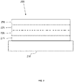
- FIG. 2 shows an inverted OLED 200.
- the device includes a substrate 210, a cathode 215, an emissive layer 220, a hole transport layer 225, and an anode 230.
- Device 200 may be fabricated by depositing the layers described, in order. Because the most common OLED configuration has a cathode disposed over the anode, and device 200 has cathode 215 disposed under anode 230, device 200 may be referred to as an "inverted" OLED. Materials similar to those described with respect to device 100 may be used in the corresponding layers of device 200.
- FIG. 2 provides one example of how some layers may be omitted from the structure of device 100.
- FIGS. 1 and 2 The simple layered structure illustrated in FIGS. 1 and 2 is provided by way of nonlimiting example, and it is understood that embodiments of the invention may be used in connection with a wide variety of other structures.
- the specific materials and structures described are exemplary in nature, and other materials and structures may be used.
- Functional OLEDs may be achieved by combining the various layers described in different ways, or layers may be omitted entirely, based on design, performance, and cost factors. Other layers not specifically described may also be included. Materials other than those specifically described may be used. Although many of the examples provided herein describe various layers as comprising a single material, it is understood that combinations of materials, such as a mixture of host and dopant, or more generally a mixture, may be used. Also, the layers may have various sublayers.
- hole transport layer 225 transports holes and injects holes into emissive layer 220, and may be described as a hole transport layer or a hole injection layer.
- an OLED may be described as having an "organic layer" disposed between a cathode and an anode. This organic layer may comprise a single layer, or may further comprise multiple layers of different organic materials as described, for example, with respect to FIGS. 1 and 2 .
- OLEDs comprised of polymeric materials (PLEDs) such as disclosed in U.S. Pat. No. 5,247,190 to Friend et al. .
- PLEDs polymeric materials
- OLEDs having a single organic layer may be used.
- OLEDs may be stacked, for example as described in U.S. Pat. No. 5,707,745 to Forrest et al.
- the OLED structure may deviate from the simple layered structure illustrated in FIGS. 1 and 2 .
- the substrate may include an angled reflective surface to improve out-coupling, such as a mesa structure as described in U.S. Pat. No. 6,091,195 to Forrest et al. , and/or a pit structure as described in U.S. Pat. No. 5,834,893 to Bulovic et al. .
- any of the layers of the various embodiments may be deposited by any suitable method.
- preferred methods include thermal evaporation, ink-jet, such as described in U.S. Pat. Nos. 6,013,982 and 6,087,196 , organic vapor phase deposition (OVPD), such as described in U.S. Pat. No. 6,337,102 to Forrest et al. , and deposition by organic vapor jet printing (OVJP), such as described in U.S. Pat. No. 7,431,968 .
- OVPD organic vapor phase deposition
- OJP organic vapor jet printing
- Other suitable deposition methods include spin coating and other solution based processes. Solution based processes are preferably carried out in nitrogen or an inert atmosphere.
- preferred methods include thermal evaporation.
- Preferred patterning methods include deposition through a mask, cold welding such as described in U.S. Pat. Nos. 6,294,398 and 6,468,819 , and patterning associated with some of the deposition methods such as ink-jet and organic vapor jet printing (OVJP). Other methods may also be used.
- the materials to be deposited may be modified to make them compatible with a particular deposition method. For example, substituents such as alkyl and aryl groups, branched or unbranched, and preferably containing at least 3 carbons, may be used in small molecules to enhance their ability to undergo solution processing. Substituents having 20 carbons or more may be used, and 3-20 carbons is a preferred range. Materials with asymmetric structures may have better solution processibility than those having symmetric structures, because asymmetric materials may have a lower tendency to recrystallize. Dendrimer substituents may be used to enhance the ability of small molecules to undergo solution processing.
- Devices fabricated in accordance with embodiments of the present invention may further optionally comprise a barrier layer.
- a barrier layer One purpose of the barrier layer is to protect the electrodes and organic layers from damaging exposure to harmful species in the environment including moisture, vapor and/or gases, etc.
- the barrier layer may be deposited over, under or next to a substrate, an electrode, or over any other parts of a device including an edge.
- the barrier layer may comprise a single layer, or multiple layers.
- the barrier layer may be formed by various known chemical vapor deposition techniques and may include compositions having a single phase as well as compositions having multiple phases. Any suitable material or combination of materials may be used for the barrier layer.
- the barrier layer may incorporate an inorganic or an organic compound or both.
- the preferred barrier layer comprises a mixture of a polymeric material and a non-polymeric material as described in U.S. Pat. No. 7,968,146 , PCT Pat. Application Nos. PCT/US2007/023098 and PCT/US2009/042829 .
- the aforesaid polymeric and non-polymeric materials comprising the barrier layer should be deposited under the same reaction conditions and/or at the same time.
- the weight ratio of polymeric to non-polymeric material may be in the range of 95:5 to 5:95.
- the polymeric material and the non-polymeric material may be created from the same precursor material.
- the mixture of a polymeric material and a non-polymeric material consists essentially of polymeric silicon and inorganic silicon.
- Devices fabricated in accordance with embodiments of the invention can be incorporated into a wide variety of electronic component modules (or units) that can be incorporated into a variety of electronic products or intermediate components. Examples of such electronic products or intermediate components include display screens, lighting devices such as discrete light source devices or lighting panels, etc. that can be utilized by the end-user product manufacturers. Such electronic component modules can optionally include the driving electronics and/or power source(s). Devices fabricated in accordance with embodiments of the invention can be incorporated into a wide variety of consumer products that have one or more of the electronic component modules (or units) incorporated therein.
- a consumer product comprising an OLED that includes the compound of the present disclosure in the organic layer in the OLED is disclosed.
- Such consumer products would include any kind of products that include one or more light source(s) and/or one or more of some type of visual displays.
- Some examples of such consumer products include flat panel displays, curved displays, computer monitors, medical monitors, televisions, billboards, lights for interior or exterior illumination and/or signaling, heads-up displays, fully or partially transparent displays, flexible displays, rollable displays, foldable displays, stretchable displays, laser printers, telephones, mobile phones, tablets, phablets, personal digital assistants (PDAs), wearable devices, laptop computers, digital cameras, camcorders, viewfinders, micro-displays (displays that are less than 2 inches diagonal), 3-D displays, virtual reality or augmented reality displays, vehicles, video walls comprising multiple displays tiled together, theater or stadium screen, a light therapy device, and a sign.
- control mechanisms may be used to control devices fabricated in accordance with the present invention, including passive matrix and active matrix. Many of the devices are intended for use in a temperature range comfortable to humans, such as 18 degrees C. to 30 degrees C., and more preferably at room temperature (20-25 degrees C), but could be used outside this temperature range, for example, from -40 degree C to + 80 degree C.
- the materials and structures described herein may have applications in devices other than OLEDs.
- other optoelectronic devices such as organic solar cells and organic photodetectors may employ the materials and structures.
- organic devices such as organic transistors, may employ the materials and structures.
- halo halogen
- halide halogen
- fluorine chlorine, bromine, and iodine
- acyl refers to a substituted carbonyl radical (C(O)-R S ).
- esters refers to a substituted oxycarbonyl (-O-C(O)-R S or -C(O)-O-R S ) radical.
- ether refers to an -OR S radical.
- sulfanyl or "thio-ether” are used interchangeably and refer to a -SR S radical.
- sulfinyl refers to a -S(O)-R S radical.
- sulfonyl refers to a -SO 2 -R S radical.
- phosphino refers to a -P(R S ) 3 radical, wherein each R S can be same or different.
- sil refers to a -Si(R S ) 3 radical, wherein each R S can be same or different.
- boryl refers to a -B(R s ) 2 radical or its Lewis adduct -B(R s ) 3 radical, wherein R s can be same or different.
- R S can be hydrogen or a substituent selected from the group consisting of deuterium, halogen, alkyl, cycloalkyl, heteroalkyl, heterocycloalkyl, arylalkyl, alkoxy, aryloxy, amino, silyl, alkenyl, cycloalkenyl, heteroalkenyl, alkynyl, aryl, heteroaryl, and combination thereof.
- Preferred R s is selected from the group consisting of alkyl, cycloalkyl, aryl, heteroaryl, and combination thereof.
- alkyl refers to and includes both straight and branched chain alkyl radicals.
- Preferred alkyl groups are those containing from one to fifteen carbon atoms and includes methyl, ethyl, propyl, 1-methylethyl, butyl, 1-methylpropyl, 2-methylpropyl, pentyl, 1-methylbutyl, 2-methylbutyl, 3-methylbutyl, 1,1-dimethylpropyl, 1,2-dimethylpropyl, 2,2-dimethylpropyl,and the like. Additionally, the alkyl group is optionally substituted.
- cycloalkyl refers to and includes monocyclic, polycyclic, and spiro alkyl radicals.
- Preferred cycloalkyl groups are those containing 3 to 12 ring carbon atoms and includes cyclopropyl, cyclopentyl, cyclohexyl, bicyclo[3.1.1]heptyl, spiro[4.5]decyl, spiro[5.5]undecyl, adamantyl, and the like. Additionally, the cycloalkyl group is optionally substituted.
- heteroalkyl or “heterocycloalkyl” refer to an alkyl or a cycloalkyl radical, respectively, having at least one carbon atom replaced by a heteroatom.
- the at least one heteroatom is selected from O, S, N, P, B, Si and Se, preferably, O, S or N.
- the heteroalkyl or heterocycloalkyl group is optionally substituted.
- alkenyl refers to and includes both straight and branched chain alkene radicals.
- Alkenyl groups are essentially alkyl groups that include at least one carbon-carbon double bond in the alkyl chain.
- Cycloalkenyl groups are essentially cycloalkyl groups that include at least one carbon-carbon double bond in the cycloalkyl ring.
- heteroalkenyl refers to an alkenyl radical having at least one carbon atom replaced by a heteroatom.
- the at least one heteroatom is selected from O, S, N, P, B, Si, and Se, preferably, O, S, or N.
- Preferred alkenyl, cycloalkenyl, or heteroalkenyl groups are those containing two to fifteen carbon atoms. Additionally, the alkenyl, cycloalkenyl, or heteroalkenyl group is optionally substituted.
- alkynyl refers to and includes both straight and branched chain alkyne radicals. Preferred alkynyl groups are those containing two to fifteen carbon atoms. Additionally, the alkynyl group is optionally substituted.
- aralkyl or “arylalkyl” are used interchangeably and refer to an alkyl group that is substituted with an aryl group. Additionally, the aralkyl group is optionally substituted.
- heterocyclic group refers to and includes aromatic and non-aromatic cyclic radicals containing at least one heteroatom.
- the at least one heteroatom is selected from O, S, N, P, B, Si, and Se, preferably, O, S, or N.
- Hetero-aromatic cyclic radicals may be used interchangeably with heteroaryl.
- Preferred hetero-non-aromatic cyclic groups are those containing 3 to 7 ring atoms which includes at least one hetero atom, and includes cyclic amines such as morpholino, piperidino, pyrrolidino, and the like, and cyclic ethers/thio-ethers, such as tetrahydrofuran, tetrahydropyran, tetrahydrothiophene, and the like. Additionally, the heterocyclic group may be optionally substituted.
- aryl refers to and includes both single-ring aromatic hydrocarbyl groups and polycyclic aromatic ring systems.
- the polycyclic rings may have two or more rings in which two carbons are common to two adjoining rings (the rings are "fused") wherein at least one of the rings is an aromatic hydrocarbyl group, e.g., the other rings can be cycloalkyls, cycloalkenyls, aryl, heterocycles, and/or heteroaryls.
- Preferred aryl groups are those containing six to thirty carbon atoms, preferably six to twenty carbon atoms, more preferably six to twelve carbon atoms. Especially preferred is an aryl group having six carbons, ten carbons or twelve carbons.
- Suitable aryl groups include phenyl, biphenyl, triphenyl, triphenylene, tetraphenylene, naphthalene, anthracene, phenalene, phenanthrene, fluorene, pyrene, chrysene, perylene, and azulene, preferably phenyl, biphenyl, triphenyl, triphenylene, fluorene, and naphthalene. Additionally, the aryl group is optionally substituted.
- heteroaryl refers to and includes both single-ring aromatic groups and polycyclic aromatic ring systems that include at least one heteroatom.
- the heteroatoms include, but are not limited to O, S, N, P, B, Si, and Se. In many instances, O, S, or N are the preferred heteroatoms.
- Hetero-single ring aromatic systems are preferably single rings with 5 or 6 ring atoms, and the ring can have from one to six heteroatoms.
- the hetero-polycyclic ring systems can have two or more rings in which two atoms are common to two adjoining rings (the rings are "fused") wherein at least one of the rings is a heteroaryl, e.g., the other rings can be cycloalkyls, cycloalkenyls, aryl, heterocycles, and/or heteroaryls.
- the hetero-polycyclic aromatic ring systems can have from one to six heteroatoms per ring of the polycyclic aromatic ring system.
- Preferred heteroaryl groups are those containing three to thirty carbon atoms, preferably three to twenty carbon atoms, more preferably three to twelve carbon atoms.
- Suitable heteroaryl groups include dibenzothiophene, dibenzofuran, dibenzoselenophene, furan, thiophene, benzofuran, benzothiophene, benzoselenophene, carbazole, indolocarbazole, pyridylindole, pyrrolodipyridine, pyrazole, imidazole, triazole, oxazole, thiazole, oxadiazole, oxatriazole, dioxazole, thiadiazole, pyridine, pyridazine, pyrimidine, pyrazine, triazine, oxazine, oxathiazine, oxadiazine, indole, benzimidazole, indazole, indoxazine, benzoxazole, benzisoxazole, benzothiazole, quinoline, isoquinoline, cinnoline, qui
- aryl and heteroaryl groups listed above the groups of triphenylene, naphthalene, anthracene, dibenzothiophene, dibenzofuran, dibenzoselenophene, carbazole, indolocarbazole, imidazole, pyridine, pyrazine, pyrimidine, triazine, and benzimidazole, and the respective aza-analogs of each thereof are of particular interest.
- alkyl, cycloalkyl, heteroalkyl, heterocycloalkyl, alkenyl, cycloalkenyl, heteroalkenyl, alkynyl, aralkyl, heterocyclic group, aryl, and heteroaryl, as used herein, are independently unsubstituted, or independently substituted, with one or more general substituents.
- the general substituents are selected from the group consisting of deuterium, halogen, alkyl, cycloalkyl, heteroalkyl, heterocycloalkyl, arylalkyl, alkoxy, aryloxy, amino, silyl, alkenyl, cycloalkenyl, heteroalkenyl, alkynyl, aryl, heteroaryl, acyl, carboxylic acid, ether, ester, nitrile, isonitrile, sulfanyl, sulfinyl, sulfonyl, phosphino, boryl, and combinations thereof.
- the preferred general substituents are selected from the group consisting of deuterium, fluorine, alkyl, cycloalkyl, heteroalkyl, alkoxy, aryloxy, amino, silyl, alkenyl, cycloalkenyl, heteroalkenyl, aryl, heteroaryl, nitrile, isonitrile, sulfanyl, boryl, and combinations thereof.
- the more preferred general substituents are selected from the group consisting of deuterium, fluorine, alkyl, cycloalkyl, alkoxy, aryloxy, amino, silyl, aryl, heteroaryl, sulfanyl, and combinations thereof.
- the most preferred general substituents are selected from the group consisting of deuterium, fluorine, alkyl, cycloalkyl, aryl, heteroaryl, and combinations thereof.
- substituted and substitution refer to a substituent other than H that is bonded to the relevant position, e.g., a carbon or nitrogen.
- R 1 when R 1 represents monosubstitution, then one R 1 must be other than H (i.e., a substitution). Similarly, when R 1 represents disubstitution, then two of R 1 must be other than H.
- R 1 when R 1 represents no substitution, R 1 , for example, can be a hydrogen for available valencies of ring atoms, as in carbon atoms for benzene and the nitrogen atom in pyrrole, or simply represents nothing for ring atoms with fully filled valencies, e.g., the nitrogen atom in pyridine.
- the maximum number of substitutions possible in a ring structure will depend on the total number of available valencies in the ring atoms.
- substitution includes a combination of two to four of the listed groups.
- substitution includes a combination of two to three groups.
- substitution includes a combination of two groups.
- Preferred combinations of substituent groups are those that contain up to fifty atoms that are not hydrogen or deuterium, or those which include up to forty atoms that are not hydrogen or deuterium, or those that include up to thirty atoms that are not hydrogen or deuterium. In many instances, a preferred combination of substituent groups will include up to twenty atoms that are not hydrogen or deuterium.
- aza-dibenzofuran i.e. aza-dibenzofuran, azadibenzothiophene, etc.
- azatriphenylene encompasses both dibenzo[ f , h ]quinoxaline and dibenzo[ f , h ]quinoline.
- deuterium refers to an isotope of hydrogen.
- Deuterated compounds can be readily prepared using methods known in the art. For example, U.S. Pat. No. 8,557,400 , Patent Pub. No. WO 2006/095951 , and U.S. Pat. Application Pub. No. US 2011/0037057 , describe the making of deuterium-substituted organometallic complexes. Further reference is made to Ming Yan, et al., Tetrahedron 2015, 71, 1425-30 and Atzrodt et al., Angew. Chem. Int. Ed. (Reviews) 2007, 46, 7744-65 , describe the deuteration of the methylene hydrogens in benzyl amines and efficient pathways to replace aromatic ring hydrogens with deuterium, respectively.
- a pair of adjacent substituents can be optionally joined or fused into a ring.
- the preferred ring is a five, six, or seven-membered carbocyclic or heterocyclic ring, includes both instances where the portion of the ring formed by the pair of substituents is saturated and where the portion of the ring formed by the pair of substituents is unsaturated.
- "adjacent" means that the two substituents involved can be on the same ring next to each other, or on two neighboring rings having the two closest available substitutable positions, such as 2, 2' positions in a biphenyl, or 1, 8 position in a naphthalene, as long as they can form a stable fused ring system.
- OLED organic light emitting device
- each R, R', R", R A , R B , R C , R D , R E , and R F is independently a hydrogen or a substituent selected from the group consisting of the preferred general substituents defined herein.
- the closest calculated intramolecular contact between the carbene carbon C A and the next nearest closest non-hydrogen atomic position of any substituent group on the ring A excluding the heavy atom of any substituent R directly attached to the N of ring A in the compound at 0 K is greater than or equal to 2.70 ⁇ .
- the structure of the compound used to measure this distance was derived from the ground state geometry of the molecular structure calculated using Gaussian 09, Revision D.01 with the B3LYP functional applying the Grimme dispersion correction, a 6-31G ⁇ basis set for host structures and CEP-31G for emitter structures.
- the ground state molecular structure of the platinum emitter was used to measure the closest intramolecular contact between the carbene carbon, C A , and the next nearest closest non-hydrogen atomic position of any substituent group on the ring A excluding the heavy atom of any substituent R directly attached to of the N of ring A, in units of ⁇ ngström.
- the closest calculated intermolecular distance between the carbene carbon C A and a non-hydrogen atom in a compound of Formula III or Formula IV, shown below, in an amorphous film configuration at 0 K is greater than or equal to 2.70 ⁇ .
- To measure the equivalent intermolecular close contact it is necessary to find low energy bimolecular pairs between host like molecules, compounds of Formula III and Formula IV, and the emitter itself that will occur in the emissive layer of an OLED device. To model the most favorable low energy pairwise structures the following procedure was used.
- the ground state B3LYP structures served as input for a Metropolis Monte Carlo simulated annealing sampling of molecular pairs using BIOVIA Materials Studio, Release 18.1, with the Adsorption Locator tool.
- rings B, C, and D are each 6-membered aromatic rings.
- ring B is a pyridine ring.
- L 1 is a direct bond. In some embodiments, L 3 is a direct bond. In some embodiments, L 2 is O.
- R A comprises a group having a structure of Formula II.
- R D comprises a group having a structure of Formula II.
- [X] comprises a benzene ring. In some embodiments, [X] comprises carbazole.
- Y 1 to Y 3 are each a direct bond. In some embodiments, one of Y 1 to Y 3 is O, and the remainder are direct bonds. In some embodiments, one of X 2 , X 5 , and X 8 is N, and the others are C. In some embodiments, X 2 is N, X 1 is C, and X 3 to X 9 are each C.
- the closest calculated intramolecular contact between the carbene carbon C A and any other non-hydrogen atom in the compound at 0 K is greater than or equal to 2.90 ⁇ . In some embodiments, the closest calculated intramolecular contact between the carbene carbon C A and any other non-hydrogen atom in the compound at 0 K is greater than or equal to 2.90 ⁇ . In some embodiments, the closest calculated intramolecular contact between the carbene carbon C A and any other non-hydrogen atom in the compound at 0 K is greater than or equal to 3.00 ⁇ . In some embodiments, the closest calculated intramolecular contact between the carbene carbon C A and any other non-hydrogen atom in the compound at 0 K is greater than or equal to 3.10 ⁇ .
- the closest calculated intermolecular distance between the carbene carbon C A and a non-hydrogen atom in a compound of Formula III or Formula IV in an amorphous film at 0 K is greater than or equal to 2.80 ⁇ . In some embodiments, the closest calculated intermolecular distance between the carbene carbon C A and a non-hydrogen atom in a compound of Formula III or Formula IV in an amorphous film at 0 K is greater than or equal to 2.90 ⁇ . In some embodiments, the closest calculated intermolecular distance between the carbene carbon C A and a non-hydrogen atom in a compound of Formula III or Formula IV in an amorphous film at 0K is greater than or equal to 3.00 ⁇ . In some embodiments, the closest calculated intermolecular distance between the carbene carbon C A and a non-hydrogen atom in a compound of Formula III or Formula IV in an amorphous film at 0 K is greater than or equal to 3.10 ⁇ .
- M is Pt.
- the group having a structure of Formula II is selected from the group consisting of: and where each R 1 to R 8 is independently selected from the group consisting of hydrogen, deuterium, alkyl, cycloalkyl, heteroalkyl, heterocycloalkyl, aryl, heteroaryl, and combinations thereof.
- the compound of Formula I is selected from the group consisting of: and
- a compound comprising a structure selected from the group consisting of is defined as in the claims; wherein, M is selected from the group consisting of Os, Pd, Pt, Ir, Cu, and Au; at least one of R A1 , R A2 , R A4 , R A5 , or R A6 is a structure of ; where Y 1A to Y 4A are each independently C or N; no more than two of Y 1A to Y 4A are N; Z 1 to Z 25 are each independently C or N; three consecutive Z 1 to Z 25 in the same ring cannot be N; R A3 , R A6 , R M , R N , R O , R X , R Y , and R Z each independently represent mono to the maximum allowable substitutions, or no substitution; each R A1 , R A2 , R A3 , R A4 , R A5 , R A6 , R M , R N , R O , R X , R Y , and R Z
- R A1 and R A2 in Formula V can be a structure of Formula VII, Formula VIII, or Formula IX.
- only at least one of R A4 and R A5 in Formula VI can be a structure of Formula VII, Formula VIII, or Formula IX.
- At least one of R A1 , R A2 , R A4 , R A5 , or R A6 comprises a chemical group containing at least three 6-membered aromatic rings that are not fused next to each other, each R A1 , R A2 , R A3 , R A4 , R A5 , and R A6 is independently a hydrogen or a substituent as defined in the claims, any adjacent substituents can be joined or fused into a ring.
- At least one of R A1 , R A2 , R A4 , R A5 , or R A6 comprises a chemical group containing at least four 6-membered aromatic rings that are not fused next to each other. In some embodiments, at least one of R A1 , R A2 , R A4 , R A5 , or R A6 comprises a chemical group containing at least five 6-membered aromatic rings that are not fused next to each other. In some embodiments, at least one of R A1 , R A2 , R A4 , R A5 , or R A6 comprises a chemical group containing at least six 6-membered aromatic rings that are not fused next to each other. In some embodiments, at least two of R A1 , R A2 , R A4 , R A5 , or R A6 comprises a chemical group containing at least three 6-membered aromatic rings that are not fused next to each other.
- each R A1 , R A2 , R A3 , R A4 , R A5 , R A6 , R M , R N , R O , R X , R Y , and R Z is independently a hydrogen or a substituent selected from the group consisting of deuterium, fluorine, alkyl, cycloalkyl, heteroalkyl, alkoxy, aryloxy, amino, silyl, alkenyl, cycloalkenyl, heteroalkenyl, aryl, heteroaryl, nitrile, isonitrile, sulfanyl, boryl, and combinations thereof.
- M is coordinated to at least one monoanionic bidentate ligand.
- Y 1A to Y 4A are each C.
- Z 1 to Z 13 are each C.
- at least one of Z 1 to Z 13 is N.
- At least one of R M , R N , and R O is a secondary or tertiary alkyl group. In some embodiments, at least one of R M , R N , and R O is a fully or partially deuterated of alkyl, cycloalkyl, heterocycloalkyl, aryl, heteroaryl group, and combinations thereof. In some embodiments, Z 14 to Z 25 are each C. In some embodiments, at least one of Z 14 to Z 25 is N.
- At least one R X is selected from the group consisting of alkyl, cycloalkyl, heteroalkyl, heterocycloalkyl, aryl, heteroaryl, and combinations thereof.
- M is four-coordinate. In some embodiments, M is six-coordinate.
- At least one of R A1 and R A2 in Formula V, or at least one of R A4 and R A5 in Formula VI is linked with other ligands to comprise a bidentate, tridentate, tetradentate, pentadentate, or hexadentate ligand.
- M is Pd, Pt, or Ir.
- at least one of R A1 , R A2 , R A4 , R A5 , or R A6 is selected from the group consisting of:
- M is Ir, Pt, or Pd and the compound comprises a ligand L A , that is coordinated to M, selected from the group consisting of where, ring D is a 5-membered or 6-membered carbocyclic or heterocyclic ring; R D represents mono to the maximum number of allowable substitutions, or no substitution; each R D is hydrogen or a substituent selected from the group consisting of deuterium, fluorine, alkyl, cycloalkyl, heteroalkyl, alkoxy, aryloxy, amino, silyl, alkenyl, cycloalkenyl, heteroalkenyl, aryl, heteroaryl, nitrile, isonitrile, sulfanyl, boryl, and combinations thereof; and any two substituents can be joined or fused to form a ring.
- ring D is a 5-membered or 6-membered carbocyclic or heterocyclic ring
- R D represents mono to the maximum number of allowable substitutions, or no
- ring D is a 6-membered aromatic ring.
- X 8 is C.
- each R A3 and R A6 is independently selected from the group consisting of hydrogen, deuterium, alkyl, cycloalkyl, heteroalkyl, heterocycloalkyl, aryl, heteroaryl, and combinations thereof.
- R A1 and R A4 are independently selected from the group consisting of alkyl, cycloalkyl, heteroalkyl, heterocycloalkyl, aryl, heteroaryl, and combinations thereof.
- R A1 and R A4 are each independently selected from the group consisting of Formula VII, Formula VIII, and Formula IX, defined above.
- the ligand L A is selected from the group consisting of:
- the ligand L A is preferably selected from the group consisting of
- the compound where the ligand L A is selected from the group consisting of Formula X and Formula XI, the compound has a formula of M(L A ) x (L B ) y (L C ) z where L B and L C are each a bidentate ligand; x is 1, 2, or 3; y is 0, 1, or 2; z is 0, 1, or 2; and x+y+z is the oxidation state of the metal M.
- the compound has a formula selected from the group consisting of Ir(L A ) 3 , Ir(L A )(L B ) 2 , Ir(L A ) 2 (L B ), Ir(L A ) 2 (L C ), and Ir(L A )(L B )(L C ); and L A , L B , and L C are different from each other.
- the compound has a formula of Pt(L A )(L B ); and L A and L B can be same or different.
- L A and L B can be connected to form a tetradentate ligand.
- L B and L C are each independently selected from the group consisting of:
- the compound is the Compound Ax having the formula Ir(L A i ) 3 or the Compound B y having the formula Ir(L A i ) 2 (L B l ), or the Compound Cz having the formula Ir(L A i )(L B l ) 2 ;
- Compound B y and Compound Cz having one of the following L B l are preferred: L B1 , L B2 , L B18 , L B28 , L B38 , L B108 , L B118 , L B122 , L B124 , L B126 , L B128 , L B130 , L B32 , L B134 , L B136 , L B138 , L B140 , L B142 , L B144 , L B156 , L B58 , L B160 , L B162 , L B164 , L B168 , L B172 , L B175 , L B204 , L B206 , L B214 , L B216 , L B218 , L B220 , L B222 , L B231 , L B233 , L B235 , L B237 , L B240 , L B242 , L B244 , L B246 , L B248 , L B
- Compound B y and Compound Cz having one of the following L B l are more preferred: L B1 , L B2 , L B18 , L B28 , L B38 , L B108 , L B118 , L B122 , L B124 , L B126 , L B128 , L B132 , L B136 , L B138 , L B142 , L B156 , L B162 , L B204 , L B206 , L B214 , L B216 , L B218 , L B220 , L B231 , L B233 , and L B237 .
- the compound is selected from the group consisting of Formula XII and Formula XIII where, M is Pd or Pt; rings B, C, and D are each independently a 5-membered or 6-membered carbocyclic or heterocyclic ring; X 1 to X 9 are each independently C or N; Y 1 to Y 3 are each independently selected from the group consisting of a direct bond, O, and S; at least one of Y 1 to Y 3 is a direct bond; Y 1A to Y 4A are each independently C or N; L 1 to L 3 are each independently selected from the group consisting of a direct bond, O, S, CR'R", SiR'R", BR', and NR', alkyl, cycloalkyl, heteroalkyl, heterocycloalkyl, aryl, and heteroaryl; m and n are each independently 0 or 1; at least one of
- rings B, C, and D are each 6-membered aromatic rings.
- ring D is phenyl.
- ring C is phenyl.
- ring B is selected from the group consisting of phenyl, pyridine, pyridazine, pyrimidine, pyrazine, triazine, imidazole, and imidazole-derived carbene.
- L 2 is O, NR', or CR'R".
- X 2 is N and X 5 is C.
- X 5 is C and X 2 is N.
- L 1 is a direct bond.
- L 1 is NR'.
- L 3 is a direct bond.
- Y 1 ,Y 2 , and Y 3 are each direct bonds.
- one of Y 1 ,Y 2 , and Y 3 is O, the remaining of Y 1 ,Y 2 , and Y 3 are each direct bonds.
- X 1 , X 3 , and X 4 are each C.
- m + n is 2.
- X 8 is C.
- Y 1A to Y 4A are each C.
- the compound can be selected from the group consisting of: and where R is selected from the group consisting of alkyl, cycloalkyl, heteroalkyl, heterocycloalkyl, aryl, heteroaryl, and combinations thereof; R P has the same definition as R B and R C ; and any two substituents may be joined or fused together to form a ring.
- the compound is selected from the group consisting of:
- OLED organic light emitting device
- the OLED comprises: an anode; a cathode; and an organic layer, disposed between the anode and the cathode, wherein the organic layer comprises a compound of where, M is Pd or Pt; rings B, C, and D are each independently a 5-membered or 6-membered carbocyclic or heterocyclic ring; X 1 to X 9 are each independently C or N; Y 1 to Y 3 are each independently selected from the group consisting of a direct bond, O, and S; at least one of Y 1 to Y 3 is a direct bond; C A is a carbene carbon; L 1 to L 3 are each independently selected from the group consisting of a direct bond, O, S, CR'R", SiR'R", BR', and NR', alkyl, cycloalkyl, heteroalkyl, heterocycloalkyl, aryl, and heteroaryl; m and
- the organic layer comprises a compound comprising a structure selected from the group consisting of: where,
- the organic layer can be an emissive layer and the compound can be is an emissive dopant or a non-emissive dopant.
- the organic layer further comprises a host, wherein host comprises at least one chemical group selected from the group consisting of triphenylene, carbazole, dibenzothiophene, dibenzofuran, dibenzoselenophene, azatriphenylene, azacarbazole, aza-dibenzothiophene, aza-dibenzofuran, and aza-dibenzoselenophene.
- the host is selected from the group consisting of: , and combinations thereof.
- a consumer product comprising the OLED that contains the novel compound of the present disclosure is also disclosed.
- the OLED has one or more characteristics selected from the group consisting of being flexible, being rollable, being foldable, being stretchable, and being curved. In some embodiments, the OLED is transparent or semi-transparent. In some embodiments, the OLED further comprises a layer comprising carbon nanotubes.
- the OLED further comprises a layer comprising a delayed fluorescent emitter.
- the OLED comprises a RGB pixel arrangement or white plus color filter pixel arrangement.
- the OLED is a mobile device, a hand held device, or a wearable device.
- the OLED is a display panel having less than 10 inch diagonal or 50 square inch area.
- the OLED is a display panel having at least 10 inch diagonal or 50 square inch area.
- the OLED is a lighting panel.
- the compound can be an emissive dopant.
- the compound can produce emissions via phosphorescence, fluorescence, thermally activated delayed fluorescence, i.e., TADF (also referred to as E-type delayed fluorescence; see, e . g ., U.S. Application No. 15/700,352, published on March 14, 2019 as U.S. patent application publication No. 2019/0081248 ), triplet-triplet annihilation, or combinations of these processes.
- the emissive dopant can be a racemic mixture, or can be enriched in one enantiomer.
- the compound can be homoleptic (each ligand is the same). In some embodiments, the compound can be heteroleptic (at least one ligand is different from others).
- the ligands can all be the same in some embodiments. In some other embodiments, at least one ligand is different from the other ligand(s). In some embodiments, every ligand can be different from each other. This is also true in embodiments where a ligand being coordinated to a metal can be linked with other ligands being coordinated to that metal to form a tridentate, tetradentate, pentadentate, or hexadentate ligands. Thus, where the coordinating ligands are being linked together, all of the ligands can be the same in some embodiments, and at least one of the ligands being linked can be different from the other ligand(s) in some other embodiments.
- the compound can be used as a phosphorescent sensitizer in an OLED where one or multiple layers in the OLED contains an acceptor in the form of one or more fluorescent and/or delayed fluorescence emitters.
- the compound can be used as one component of an exciplex to be used as a sensitizer.
- the compound must be capable of energy transfer to the acceptor and the acceptor will emit the energy or further transfer energy to a final emitter.
- the acceptor concentrations can range from 0.001% to 100%.
- the acceptor could be in either the same layer as the phosphorescent sensitizer or in one or more different layers.
- the acceptor is a TADF emitter.
- the acceptor is a fluorescent emitter.
- the emission can arise from any or all of the sensitizer, acceptor, and final emitter.
- the compound of the present disclosure is neutrally charged.
- a formulation comprising the compound described herein is also disclosed.
- the OLED disclosed herein can be incorporated into one or more of a consumer product, an electronic component module, and a lighting panel.
- the organic layer can be an emissive layer and the compound can be an emissive dopant in some embodiments, while the compound can be a non-emissive dopant in other embodiments.
- the organic layer can also include a host.
- a host In some embodiments, two or more hosts are preferred.
- the hosts used maybe a) bipolar, b) electron transporting, c) hole transporting or d) wide band gap materials that play little role in charge transport.
- the host can include a metal complex.
- the host can be a triphenylene containing benzo-fused thiophene or benzo-fused furan.
- n can range from 1 to 10; and Ar 1 and Ar 2 can be independently selected from the group consisting of benzene, biphenyl, naphthalene, triphenylene, carbazole, and heteroaromatic analogs thereof.
- the host can be an inorganic compound, for example, a Zn containing inorganic material e.g. ZnS.
- the host can be a compound comprising at least one chemical group selected from the group consisting of triphenylene, carbazole, dibenzothiophene, dibenzofuran, dibenzoselenophene, azatriphenylene, azacarbazole, aza-dibenzothiophene, aza-dibenzofuran, and aza-dibenzoselenophene.
- the host can include a metal complex.
- the host can be, but is not limited to, a specific compound selected from the Host Group consisting of: and combinations thereof. Additional information on possible hosts is provided below.
- the emissive region comprises a compound of Formula I where, M is Pd or Pt; rings B, C, and D are each independently a 5-membered or 6-membered carbocyclic or heterocyclic ring; X 1 to X 9 are each independently C or N; Y 1 to Y 3 are each independently selected from the group consisting of a direct bond, O, and S; at least one of Y 1 to Y 3 is a direct bond; C A is a carbene carbon; L 1 to L 3 are each independently selected from the group consisting of a direct bond, O, S, CR'R", SiR'R", BR', and NR', alkyl, cycloalkyl, heteroalkyl, heterocycloalkyl, aryl, and heteroaryl; m and n are each independently 0 or 1; at least one of m and n is 1; at least one of R, R A , R B , R C , R
- the emissive region comprises a compound comprising a structure of a formula selected from the group consisting of where,
- the compound can be an emissive dopant or a non-emissive dopant.
- the emissive region further comprises a host, wherein the host contains at least one group selected from the group consisting of metal complex, triphenylene, carbazole, dibenzothiophene, dibenzofuran, dibenzoselenophene, azatriphenylene, aza-carbazole, aza-dibenzothiophene, aza-dibenzofuran, and aza-dibenzoselenophene.
- the emissive region further comprises a host, where the host is selected from the Host Group defined herein.
- a formulation that comprises the novel compound disclosed herein is described.
- the formulation can include one or more components selected from the group consisting of a solvent, a host, a hole injection material, hole transport material, electron blocking material, hole blocking material, and an electron transport material, disclosed herein.
- the present disclosure encompasses any chemical structure comprising the novel compound of the present disclosure, or a monovalent or polyvalent variant thereof.
- the inventive compound, or a monovalent or polyvalent variant thereof can be a part of a larger chemical structure.
- Such chemical structure can be selected from the group consisting of a monomer, a polymer, a macromolecule, and a supramolecule (also known as supermolecule).
- a "monovalent variant of a compound” refers to a moiety that is identical to the compound except that one hydrogen has been removed and replaced with a bond to the rest of the chemical structure.
- a "polyvalent variant of a compound” refers to a moiety that is identical to the compound except that more than one hydrogen has been removed and replaced with a bond or bonds to the rest of the chemical structure. In the instance of a supramolecule, the inventive compound is can also be incorporated into the supramolecule complex without covalent bonds.
- the materials described herein as useful for a particular layer in an organic light emitting device may be used in combination with a wide variety of other materials present in the device.
- emissive dopants disclosed herein may be used in conjunction with a wide variety of hosts, transport layers, blocking layers, injection layers, electrodes and other layers that may be present.
- the materials described or referred to below are non-limiting examples of materials that may be useful in combination with the compounds disclosed herein, and one of skill in the art can readily consult the literature to identify other materials that may be useful in combination.
- a charge transport layer can be doped with conductivity dopants to substantially alter its density of charge carriers, which will in turn alter its conductivity.
- the conductivity is increased by generating charge carriers in the matrix material, and depending on the type of dopant, a change in the Fermi level of the semiconductor may also be achieved.
- Hole-transporting layer can be doped by p-type conductivity dopants and n-type conductivity dopants are used in the electron-transporting layer.
- Non-limiting examples of the conductivity dopants that may be used in an OLED in combination with materials disclosed herein are exemplified below together with references that disclose those materials: EP01617493 , EP01968131 , EP2020694 , EP2684932 , US20050139810 , US20070160905 , US20090167167 , US2010288362 , WO06081780 , WO2009003455 , WO2009008277 , WO2009011327 , WO2014009310 , US2007252140 , US2015060804 , US20150123047 , and US2012146012 .
- a hole injecting/transporting material to be used in the present invention is not particularly limited, and any compound may be used as long as the compound is typically used as a hole injecting/transporting material.
- the material include, but are not limited to: a phthalocyanine or porphyrin derivative; an aromatic amine derivative; an indolocarbazole derivative; a polymer containing fluorohydrocarbon; a polymer with conductivity dopants; a conducting polymer, such as PEDOT/PSS; a self-assembly monomer derived from compounds such as phosphonic acid and silane derivatives; a metal oxide derivative, such as MoO x ; a p-type semiconducting organic compound, such as 1,4,5,8,9,12-Hexaazatriphenylenehexacarbonitrile; a metal complex, and a crosslinkable compounds.
- aromatic amine derivatives used in HIL or HTL include, but not limit to the following general structures:
- Each of Ar 1 to Ar 9 is selected from the group consisting of aromatic hydrocarbon cyclic compounds such as benzene, biphenyl, triphenyl, triphenylene, naphthalene, anthracene, phenalene, phenanthrene, fluorene, pyrene, chrysene, perylene, and azulene; the group consisting of aromatic heterocyclic compounds such as dibenzothiophene, dibenzofuran, dibenzoselenophene, furan, thiophene, benzofuran, benzothiophene, benzoselenophene, carbazole, indolocarbazole, pyridylindole, pyrrolodipyridine, pyrazole, imidazole, triazole, oxazole, thiazole, oxadiazole, oxatriazole, dioxazole, thiadiazole, pyridine, pyridazine
- Each Ar may be unsubstituted or may be substituted by a substituent selected from the group consisting of deuterium, halogen, alkyl, cycloalkyl, heteroalkyl, heterocycloalkyl, arylalkyl, alkoxy, aryloxy, amino, silyl, alkenyl, cycloalkenyl, heteroalkenyl, alkynyl, aryl, heteroaryl, acyl, carboxylic acids, ether, ester, nitrile, isonitrile, sulfanyl, sulfinyl, sulfonyl, phosphino, and combinations thereof.
- a substituent selected from the group consisting of deuterium, halogen, alkyl, cycloalkyl, heteroalkyl, heterocycloalkyl, arylalkyl, alkoxy, aryloxy, amino, silyl, alkenyl, cycloalkenyl, heteroalkeny
- Ar 1 to Ar 9 is independently selected from the group consisting of: wherein k is an integer from 1 to 20; X 101 to X 108 is C (including CH) or N; Z 101 is NAr 1 , O, or S; Ar 1 has the same group defined above.
- metal complexes used in HIL or HTL include, but are not limited to the following general formula: wherein Met is a metal, which can have an atomic weight greater than 40; (Y 101 -Y 102 ) is a bidentate ligand, Y 101 and Y 102 are independently selected from C, N, O, P, and S; L 101 is an ancillary ligand; k' is an integer value from 1 to the maximum number of ligands that may be attached to the metal; and k'+k" is the maximum number of ligands that may be attached to the metal.
- (Y 101 -Y 102 ) is a 2-phenylpyridine derivative. In another aspect, (Y 101 -Y 102 ) is a carbene ligand. In another aspect, Met is selected from Ir, Pt, Os, and Zn. In a further aspect, the metal complex has a smallest oxidation potential in solution vs. Fc + /Fc couple less than about 0.6 V.
- Non-limiting examples of the HIL and HTL materials that may be used in an OLED in combination with materials disclosed herein are exemplified below together with references that disclose those materials: CN102702075 , DE102012005215 , EP01624500 , EP01698613 , EP01806334 , EP01930964 , EP01972613 , EP01997799 , EP02011790 , EP02055700 , EP02055701 , EP1725079 , EP2085382 , EP2660300 , EP650955 , JP07-073529 , JP2005112765 , JP2007091719 , JP2008021687 , JP2014-009196 , KR20110088898 , KR20130077473 , TW201139402 , US06517957 , US20020158242 , US20030162053 , US20050123751 , US20060182993 , US200602402
- An electron blocking layer may be used to reduce the number of electrons and/or excitons that leave the emissive layer.
- the presence of such a blocking layer in a device may result in substantially higher efficiencies, and/or longer lifetime, as compared to a similar device lacking a blocking layer.
- a blocking layer may be used to confine emission to a desired region of an OLED.
- the EBL material has a higher LUMO (closer to the vacuum level) and/or higher triplet energy than the emitter closest to the EBL interface.
- the EBL material has a higher LUMO (closer to the vacuum level) and/or higher triplet energy than one or more of the hosts closest to the EBL interface.
- the compound used in EBL contains the same molecule or the same functional groups used as one of the hosts described below.
- the light emitting layer of the organic EL device of the present invention preferably contains at least a metal complex as light emitting material, and may contain a host material using the metal complex as a dopant material.
- the host material are not particularly limited, and any metal complexes or organic compounds may be used as long as the triplet energy of the host is larger than that of the dopant. Any host material may be used with any dopant so long as the triplet criteria is satisfied.
- Examples of metal complexes used as host are preferred to have the following general formula: wherein Met is a metal; (Y 103 -Y 104 ) is a bidentate ligand, Y 103 and Y 104 are independently selected from C, N, O, P, and S; L 101 is an another ligand; k' is an integer value from 1 to the maximum number of ligands that may be attached to the metal; and k'+k" is the maximum number of ligands that may be attached to the metal.
- the metal complexes are: wherein (O-N) is a bidentate ligand, having metal coordinated to atoms O and N.
- Met is selected from Ir and Pt.
- (Y 103 -Y 104 ) is a carbene ligand.
- the host compound contains at least one of the following groups selected from the group consisting of aromatic hydrocarbon cyclic compounds such as benzene, biphenyl, triphenyl, triphenylene, tetraphenylene, naphthalene, anthracene, phenalene, phenanthrene, fluorene, pyrene, chrysene, perylene, and azulene; the group consisting of aromatic heterocyclic compounds such as dibenzothiophene, dibenzofuran, dibenzoselenophene, furan, thiophene, benzofuran, benzothiophene, benzoselenophene, carbazole, indolocarbazole, pyridylindole, pyrrolodipyridine, pyrazole, imidazole, triazole, oxazole, thiazole, oxadiazole, oxatriazole, dioxazole, thiadia
- Each option within each group may be unsubstituted or may be substituted by a substituent selected from the group consisting of deuterium, halogen, alkyl, cycloalkyl, heteroalkyl, heterocycloalkyl, arylalkyl, alkoxy, aryloxy, amino, silyl, alkenyl, cycloalkenyl, heteroalkenyl, alkynyl, aryl, heteroaryl, acyl, carboxylic acids, ether, ester, nitrile, isonitrile, sulfanyl, sulfinyl, sulfonyl, phosphino, and combinations thereof.
- the host compound contains at least one of the following groups in the molecule: and wherein R 101 is selected from the group consisting of hydrogen, deuterium, halogen, alkyl, cycloalkyl, heteroalkyl, heterocycloalkyl, arylalkyl, alkoxy, aryloxy, amino, silyl, alkenyl, cycloalkenyl, heteroalkenyl, alkynyl, aryl, heteroaryl, acyl, carboxylic acids, ether, ester, nitrile, isonitrile, sulfanyl, sulfinyl, sulfonyl, phosphino, and combinations thereof, and when it is aryl or heteroaryl, it has the similar definition as Ar's mentioned above.
- k is an integer from 0 to 20 or 1 to 20.
- X 101 to X 108 are independently selected from C (including CH) or N.
- Z 101 and Z 102 are independently selected from NR 101
- Non-limiting examples of the host materials that may be used in an OLED in combination with materials disclosed herein are exemplified below together with references that disclose those materials: EP2034538 , EP2034538A , EP2757608 , JP2007254297 , KR20100079458 , KR20120088644 , KR20120129733 , KR20130115564 , TW201329200 , US20030175553 , US20050238919 , US20060280965 , US20090017330 , US20090030202 , US20090167162 , US20090302743 , US20090309488 , US20100012931 , US20100084966 , US20100187984 , US2010187984 , US2012075273 , US2012126221 , US2013009543 , US2013105787 , US2013175519 , US2014001446 , US20140183503 , US20140225088 ,
- One or more additional emitter dopants may be used in conjunction with the compound of the present disclosure.
- the additional emitter dopants are not particularly limited, and any compounds may be used as long as the compounds are typically used as emitter materials.
- suitable emitter materials include, but are not limited to, compounds which can produce emissions via phosphorescence, fluorescence, thermally activated delayed fluorescence, i.e., TADF (also referred to as E-type delayed fluorescence), triplet-triplet annihilation, or combinations of these processes.
- Non-limiting examples of the emitter materials that may be used in an OLED in combination with materials disclosed herein are exemplified below together with references that disclose those materials: CN103694277 , CN1696137 , EB01238981 , EP01239526 , EP01961743 , EP1239526 , EP1244155 , EP1642951 , EP1647554 , EP1841834 , EP1841834B , EP2062907 , EP2730583 , JP2012074444 , JP2013110263 , JP4478555 , KR1020090133652 , KR20120032054 , KR20130043460 , TW201332980 , US06699599 , US06916554 , US20010019782 , US20020034656 , US20030068526 , US20030072964 , US20030138657 , US20050123788 , US20050244673 , US200512379
- a hole blocking layer may be used to reduce the number of holes and/or excitons that leave the emissive layer.
- the presence of such a blocking layer in a device may result in substantially higher efficiencies and/or longer lifetime as compared to a similar device lacking a blocking layer.
- a blocking layer may be used to confine emission to a desired region of an OLED.
- the HBL material has a lower HOMO (further from the vacuum level) and/or higher triplet energy than the emitter closest to the HBL interface.
- the HBL material has a lower HOMO (further from the vacuum level) and/or higher triplet energy than one or more of the hosts closest to the HBL interface.
- compound used in HBL contains the same molecule or the same functional groups used as host described above.
- compound used in HBL contains at least one of the following groups in the molecule: wherein k is an integer from 1 to 20; L 101 is an another ligand, k' is an integer from 1 to 3.
- Electron transport layer may include a material capable of transporting electrons. Electron transport layer may be intrinsic (undoped), or doped. Doping may be used to enhance conductivity. Examples of the ETL material are not particularly limited, and any metal complexes or organic compounds may be used as long as they are typically used to transport electrons.
- compound used in ETL contains at least one of the following groups in the molecule: wherein R 101 is selected from the group consisting of hydrogen, deuterium, halogen, alkyl, cycloalkyl, heteroalkyl, heterocycloalkyl, arylalkyl, alkoxy, aryloxy, amino, silyl, alkenyl, cycloalkenyl, heteroalkenyl, alkynyl, aryl, heteroaryl, acyl, carboxylic acids, ether, ester, nitrile, isonitrile, sulfanyl, sulfinyl, sulfonyl, phosphino, and combinations thereof, when it is aryl or heteroaryl, it has the similar definition as Ar's mentioned above.
- Ar 1 to Ar 3 has the similar definition as Ar's mentioned above.
- k is an integer from 1 to 20.
- X 101 to X 108 is selected from C (including CH) or N.
- the metal complexes used in ETL contains, but not limit to the following general formula: wherein (O-N) or (N-N) is a bidentate ligand, having metal coordinated to atoms O, N or N, N; L 101 is another ligand; k' is an integer value from 1 to the maximum number of ligands that may be attached to the metal.
- Non-limiting examples of the ETL materials that may be used in an OLED in combination with materials disclosed herein are exemplified below together with references that disclose those materials: CN103508940 , EP01602648 , EP01734038 , EP01956007 , JP2004-022334 , JP2005149918 , JP2005-268199 , KR0117693 , KR20130108183 , US20040036077 , US20070104977 , US2007018155 , US20090101870 , US20090115316 , US20090140637 , US20090179554 , US2009218940 , US2010108990 , US2011156017 , US2011210320 , US2012193612 , US2012214993 , US2014014925 , US2014014927 , US20140284580 , US6656612 , US8415031 , WO2003060956 , WO2007111263 , WO
- the CGL plays an essential role in the performance, which is composed of an n-doped layer and a p-doped layer for injection of electrons and holes, respectively. Electrons and holes are supplied from the CGL and electrodes. The consumed electrons and holes in the CGL are refilled by the electrons and holes injected from the cathode and anode, respectively; then, the bipolar currents reach a steady state gradually.
- Typical CGL materials include n and p conductivity dopants used in the transport layers.
- the hydrogen atoms can be partially or fully deuterated.
- any specifically listed substituent such as, without limitation, methyl, phenyl, pyridyl, etc. may be undeuterated, partially deuterated, and fully deuterated versions thereof.
- classes of substituents such as, without limitation, alkyl, aryl, cycloalkyl, heteroaryl, etc. also may be undeuterated, partially deuterated, and fully deuterated versions thereof.
- Table 1 shows emission peak, PLQY, and excited state lifetime for the inventive Compound 60253535971, 59736162506, 59735728275, 62201598409, 59735140786, and 59221752029. All inventive compounds showed higher PLQYs and shorter excited state lifetime, indicating the bulky group around the metal preserves compound's emissivity. Their emissions in PMMA are in a range of 455-458 nm, which are excellent candidate for generating saturate blue for display application.
- N1-(5′,5′′′-diphenyl-[1,1′:3′,1 ⁇ :3 ⁇ ,1′′′:3′′′,1 ⁇ -quinquephenyl]-2 ⁇ -yl)benzene-1,2-diamine A mixture of N1-(2,6-dibromophenyl)benzene-1,2-diamine (1 g, 2.92 mmol), [1,1':3',1"-terphenyl]-5'-ylboronic acid (2.404 g, 8.77 mmol), tetrakis(triphenylphosphine)palladium(0) (0.169 g, 0.146 mmol), and potassium phosphate (1.862 g, 8.77 mmol) was vacuumed and back-filled with nitrogen.
- the reaction was heated at 125 °C for total of 68 hours.
- the mixture was concentrated under reduced pressure, dissolved in DCM (200 mL), absorbed on to Celite and purified on silica eluting with 40-55% DCM in hexanes (46% yield).
- reaction mixture was cooled down to room temperature and poured into 200 mL sat. NaHCO 3 .
- the mixture was extracted with EtOAc and dried over sodium sulfate and concentrated.
- the crude product was coated on Celite and chromatographed on silica eluting with 40-100% DCM/Hex to give products as brown solid (59% yield).
- the tube was sealed and the reaction was heated at 140°C for 16 hours. After cooling to room temperature, the crude reaction mixture was concentrated and adsorbed onto silica gel (50 g) and purified by chromatography on silica, eluting with a gradient of 5% methanol in dichloromethane to yield product as light yellow solid (53% yield).
- N1-(4,4"-di-tert-butyl-[1,1':3',1"-terphenyl]-2'-yl)benzene-1,2-diamine To a 100 mL pressure vessel was added N1-(2,6-dibromophenyl)benzene-1,2-diamine (1 g, 2.92 mmol) in argon purged dioxane (27 mL):water mixture (9 mL), (4-(tert-butyl)phenyl)boronic acid (2.082 g, 11.69 mmol), tetrakis(triphenylphosphine)palladium(0) (0.338 g, 0.292 mmol) and potassium phosphate tribasic (1.862 g, 8.77 mmol) was added while suspension was purged with argon.
- reaction mixture was heated to 60°C for 1 hour, then heated to 225°C for 10 days.
- the reaction mixture was concentrated and absorbed to 30 g Celite and purified by column chromatography eluting with 35% DCM/Hex to give product (9.10 % yield).
- OLED device fabrication OLEDs were grown on a glass substrate pre-coated with an indium-tin-oxide (ITO) layer having a sheet resistance of 15- ⁇ /sq. Prior to any organic layer deposition or coating, the substrate was degreased with solvents and then treated with an oxygen plasma for 1.5 minutes with 50W at 13 Pa (100 mTorr) and with UV ozone for 5 minutes.
- the devices in Table21 were fabricated in high vacuum ( ⁇ 133 ⁇ 10 -6 Pa or 10 -6 Torr) by thermal evaporation.
- the anode electrode was 750 ⁇ of indium tin oxide (ITO).
- the device example had organic layers consisting of, sequentially, from the ITO surface, 100 ⁇ thick Compound A (HIL), 250 ⁇ layer of Compound B (HTL), 50 ⁇ of Compound C (EBL), 300 ⁇ of Compound D doped with 10% of Emitter (EML), 50 ⁇ of Compound E (BL), 300 ⁇ of Compound G doped with 35% of Compound F (ETL), 10 ⁇ of Compound G (EIL) followed by 1,000 ⁇ of Al (Cath). All devices were encapsulated with a glass lid sealed with an epoxy resin in a nitrogen glove box ( ⁇ 1 ppm of H 2 O and O 2 ,) immediately after fabrication with a moisture getter incorporated inside the package. Doping percentages are in volume percent. Table 2.
- Table 2 shows device data for the inventive compounds, Compound 60253535971, Compound 59736162506, Compound 59735728275, Compound 62201598409, Compound 59735140786, and Compound 59221752029, which are normalized to the Comparative one. All inventive compounds exhibit lower voltages as compared to the Comparative Example at 1000 nit. The EQE of the inventive compounds are much higher than that of Comparative Example, indicating the steric bulk is beneficial to preserve dopant's emission. Compound 59735728275 has a CIE-y of 0.148 which is comparable to that of commercial fluorescent blue.
Landscapes
- Chemical & Material Sciences (AREA)
- Organic Chemistry (AREA)
- Engineering & Computer Science (AREA)
- Materials Engineering (AREA)
- Crystallography & Structural Chemistry (AREA)
- Inorganic Chemistry (AREA)
- Physics & Mathematics (AREA)
- Optics & Photonics (AREA)
- Electroluminescent Light Sources (AREA)
Priority Applications (1)
| Application Number | Priority Date | Filing Date | Title |
|---|---|---|---|
| EP22195016.5A EP4134371A3 (en) | 2019-03-26 | 2020-03-24 | Organic electroluminescent materials and devices |
Applications Claiming Priority (9)
| Application Number | Priority Date | Filing Date | Title |
|---|---|---|---|
| US201962823922P | 2019-03-26 | 2019-03-26 | |
| US201962834666P | 2019-04-16 | 2019-04-16 | |
| US201962842230P | 2019-05-02 | 2019-05-02 | |
| US201962859919P | 2019-06-11 | 2019-06-11 | |
| US201962897667P | 2019-09-09 | 2019-09-09 | |
| US201962898219P | 2019-09-10 | 2019-09-10 | |
| US201962945273P | 2019-12-09 | 2019-12-09 | |
| US16/718,355 US11802136B2 (en) | 2017-06-23 | 2019-12-18 | Organic electroluminescent materials and devices |
| US16/807,877 US11814403B2 (en) | 2017-06-23 | 2020-03-03 | Organic electroluminescent materials and devices |
Related Child Applications (1)
| Application Number | Title | Priority Date | Filing Date |
|---|---|---|---|
| EP22195016.5A Division EP4134371A3 (en) | 2019-03-26 | 2020-03-24 | Organic electroluminescent materials and devices |
Publications (2)
| Publication Number | Publication Date |
|---|---|
| EP3715353A1 EP3715353A1 (en) | 2020-09-30 |
| EP3715353B1 true EP3715353B1 (en) | 2022-09-14 |
Family
ID=69960406
Family Applications (2)
| Application Number | Title | Priority Date | Filing Date |
|---|---|---|---|
| EP20165219.5A Active EP3715353B1 (en) | 2019-03-26 | 2020-03-24 | Organic electroluminescent materials and devices |
| EP22195016.5A Pending EP4134371A3 (en) | 2019-03-26 | 2020-03-24 | Organic electroluminescent materials and devices |
Family Applications After (1)
| Application Number | Title | Priority Date | Filing Date |
|---|---|---|---|
| EP22195016.5A Pending EP4134371A3 (en) | 2019-03-26 | 2020-03-24 | Organic electroluminescent materials and devices |
Country Status (4)
| Country | Link |
|---|---|
| EP (2) | EP3715353B1 (enExample) |
| JP (2) | JP2020158491A (enExample) |
| KR (1) | KR20200116039A (enExample) |
| CN (2) | CN117304234A (enExample) |
Families Citing this family (13)
| Publication number | Priority date | Publication date | Assignee | Title |
|---|---|---|---|---|
| KR102853328B1 (ko) * | 2020-04-24 | 2025-09-01 | 삼성디스플레이 주식회사 | 유기금속 화합물 및 이를 포함한 유기 발광 소자 |
| KR102870801B1 (ko) * | 2020-10-13 | 2025-10-14 | 삼성디스플레이 주식회사 | 유기금속 화합물, 이를 포함한 발광 소자 및 이를 포함한 전자 장치 |
| CN112500436B (zh) * | 2020-12-15 | 2022-10-18 | 浙江工业大学 | 一种铂卡宾磷光材料金属化的合成方法 |
| KR102883832B1 (ko) * | 2020-12-30 | 2025-11-10 | 삼성디스플레이 주식회사 | 유기금속 화합물, 이를 포함한 발광 소자 및 상기 발광 소자를 포함한 전자 장치 |
| KR20220126853A (ko) * | 2021-03-09 | 2022-09-19 | 삼성디스플레이 주식회사 | 유기금속 화합물 및 이를 포함한 유기 발광 소자 |
| US12421262B2 (en) * | 2021-03-15 | 2025-09-23 | Universal Display Corporation | Organic electroluminescent materials and devices |
| US20220396596A1 (en) * | 2021-05-24 | 2022-12-15 | Universal Display Corporation | Organic electroluminescent materials and devices |
| CN113201021B (zh) * | 2021-04-22 | 2022-09-30 | 浙江工业大学 | 基于1,8-取代咔唑的高辐射速率铂配合物及应用 |
| CN115557996B (zh) * | 2021-07-02 | 2025-01-21 | 南京佳诺霖光电科技有限公司 | 二价铂配合物及其作为蓝磷光材料在有机光电器件中的应用 |
| CN113773211A (zh) * | 2021-09-15 | 2021-12-10 | 中国科学院长春应用化学研究所 | 一类n、o配位的大位阻配体、镍催化剂及其制备方法与应用 |
| KR102547691B1 (ko) * | 2021-11-30 | 2023-06-27 | 삼성디스플레이 주식회사 | 조성물, 발광 소자, 및 이를 포함한 전자 장치 |
| KR102763282B1 (ko) * | 2022-07-20 | 2025-02-10 | 삼성디스플레이 주식회사 | 조성물, 발광 소자, 이를 포함한 전자 장치 및 유기금속 화합물 |
| KR20250000096A (ko) * | 2023-06-22 | 2025-01-02 | 주식회사 로오딘 | 유기발광다이오드 |
Family Cites Families (331)
| Publication number | Priority date | Publication date | Assignee | Title |
|---|---|---|---|---|
| US585108A (en) | 1897-06-22 | Bicycle luggage-carrier | ||
| US1238981A (en) | 1917-05-09 | 1917-09-04 | Bernard Cyril Barton | Press. |
| US4769292A (en) | 1987-03-02 | 1988-09-06 | Eastman Kodak Company | Electroluminescent device with modified thin film luminescent zone |
| JPH01238981A (ja) | 1988-03-22 | 1989-09-25 | Fuji Photo Film Co Ltd | 感熱記録シートの製造方法 |
| GB8909011D0 (en) | 1989-04-20 | 1989-06-07 | Friend Richard H | Electroluminescent devices |
| US5061569A (en) | 1990-07-26 | 1991-10-29 | Eastman Kodak Company | Electroluminescent device with organic electroluminescent medium |
| JPH0773529A (ja) | 1993-08-31 | 1995-03-17 | Hitachi Ltd | 光磁気記録方式および光磁気記録媒体 |
| DE69412567T2 (de) | 1993-11-01 | 1999-02-04 | Hodogaya Chemical Co., Ltd., Tokio/Tokyo | Aminverbindung und sie enthaltende Elektrolumineszenzvorrichtung |
| US5707745A (en) | 1994-12-13 | 1998-01-13 | The Trustees Of Princeton University | Multicolor organic light emitting devices |
| US5703436A (en) | 1994-12-13 | 1997-12-30 | The Trustees Of Princeton University | Transparent contacts for organic devices |
| KR0117693Y1 (ko) | 1995-03-16 | 1998-04-23 | 천일선 | 곡물볶음기의 도어개폐장치 |
| US6939625B2 (en) | 1996-06-25 | 2005-09-06 | Nôrthwestern University | Organic light-emitting diodes and methods for assembly and enhanced charge injection |
| US5844363A (en) | 1997-01-23 | 1998-12-01 | The Trustees Of Princeton Univ. | Vacuum deposited, non-polymeric flexible organic light emitting devices |
| US5834893A (en) | 1996-12-23 | 1998-11-10 | The Trustees Of Princeton University | High efficiency organic light emitting devices with light directing structures |
| US6091195A (en) | 1997-02-03 | 2000-07-18 | The Trustees Of Princeton University | Displays having mesa pixel configuration |
| US6013982A (en) | 1996-12-23 | 2000-01-11 | The Trustees Of Princeton University | Multicolor display devices |
| DE69804529T2 (de) | 1997-05-19 | 2002-10-02 | Canon Kk | Organisches Material und elektrolumineszente Vorrichtung dasselbe nutzend |
| US6413656B1 (en) | 1998-09-14 | 2002-07-02 | The University Of Southern California | Reduced symmetry porphyrin molecules for producing enhanced luminosity from phosphorescent organic light emitting devices |
| US6303238B1 (en) | 1997-12-01 | 2001-10-16 | The Trustees Of Princeton University | OLEDs doped with phosphorescent compounds |
| US6337102B1 (en) | 1997-11-17 | 2002-01-08 | The Trustees Of Princeton University | Low pressure vapor phase deposition of organic thin films |
| US6087196A (en) | 1998-01-30 | 2000-07-11 | The Trustees Of Princeton University | Fabrication of organic semiconductor devices using ink jet printing |
| US6097147A (en) | 1998-09-14 | 2000-08-01 | The Trustees Of Princeton University | Structure for high efficiency electroluminescent device |
| US6830828B2 (en) | 1998-09-14 | 2004-12-14 | The Trustees Of Princeton University | Organometallic complexes as phosphorescent emitters in organic LEDs |
| US6461747B1 (en) | 1999-07-22 | 2002-10-08 | Fuji Photo Co., Ltd. | Heterocyclic compounds, materials for light emitting devices and light emitting devices using the same |
| US6294398B1 (en) | 1999-11-23 | 2001-09-25 | The Trustees Of Princeton University | Method for patterning devices |
| US6458475B1 (en) | 1999-11-24 | 2002-10-01 | The Trustee Of Princeton University | Organic light emitting diode having a blue phosphorescent molecule as an emitter |
| US6821645B2 (en) | 1999-12-27 | 2004-11-23 | Fuji Photo Film Co., Ltd. | Light-emitting material comprising orthometalated iridium complex, light-emitting device, high efficiency red light-emitting device, and novel iridium complex |
| KR100377321B1 (ko) | 1999-12-31 | 2003-03-26 | 주식회사 엘지화학 | 피-형 반도체 성질을 갖는 유기 화합물을 포함하는 전기소자 |
| US6670645B2 (en) | 2000-06-30 | 2003-12-30 | E. I. Du Pont De Nemours And Company | Electroluminescent iridium compounds with fluorinated phenylpyridines, phenylpyrimidines, and phenylquinolines and devices made with such compounds |
| JP5241053B2 (ja) | 2000-08-11 | 2013-07-17 | ザ、トラスティーズ オブ プリンストン ユニバーシティ | 有機金属化合物及び放射移行有機電気燐光体 |
| WO2002044189A1 (fr) | 2000-11-30 | 2002-06-06 | Canon Kabushiki Kaisha | Element luminescent et afficheur |
| JP4154145B2 (ja) | 2000-12-01 | 2008-09-24 | キヤノン株式会社 | 金属配位化合物、発光素子及び表示装置 |
| US6579630B2 (en) | 2000-12-07 | 2003-06-17 | Canon Kabushiki Kaisha | Deuterated semiconducting organic compounds used for opto-electronic devices |
| JP4438042B2 (ja) | 2001-03-08 | 2010-03-24 | キヤノン株式会社 | 金属配位化合物、電界発光素子及び表示装置 |
| JP4307000B2 (ja) | 2001-03-08 | 2009-08-05 | キヤノン株式会社 | 金属配位化合物、電界発光素子及び表示装置 |
| JP4307001B2 (ja) | 2001-03-14 | 2009-08-05 | キヤノン株式会社 | 金属配位化合物、電界発光素子及び表示装置 |
| DE10116962A1 (de) | 2001-04-05 | 2002-10-10 | Covion Organic Semiconductors | Rhodium- und Iridium-Komplexe |
| US7071615B2 (en) | 2001-08-20 | 2006-07-04 | Universal Display Corporation | Transparent electrodes |
| US7431968B1 (en) | 2001-09-04 | 2008-10-07 | The Trustees Of Princeton University | Process and apparatus for organic vapor jet deposition |
| US6835469B2 (en) | 2001-10-17 | 2004-12-28 | The University Of Southern California | Phosphorescent compounds and devices comprising the same |
| US7166368B2 (en) | 2001-11-07 | 2007-01-23 | E. I. Du Pont De Nemours And Company | Electroluminescent platinum compounds and devices made with such compounds |
| US6863997B2 (en) | 2001-12-28 | 2005-03-08 | The Trustees Of Princeton University | White light emitting OLEDs from combined monomer and aggregate emission |
| KR100691543B1 (ko) | 2002-01-18 | 2007-03-09 | 주식회사 엘지화학 | 새로운 전자 수송용 물질 및 이를 이용한 유기 발광 소자 |
| US6653654B1 (en) | 2002-05-01 | 2003-11-25 | The University Of Hong Kong | Electroluminescent materials |
| JP4106974B2 (ja) | 2002-06-17 | 2008-06-25 | コニカミノルタホールディングス株式会社 | 有機エレクトロルミネッセンス素子及び表示装置 |
| US20030230980A1 (en) | 2002-06-18 | 2003-12-18 | Forrest Stephen R | Very low voltage, high efficiency phosphorescent oled in a p-i-n structure |
| US6916554B2 (en) | 2002-11-06 | 2005-07-12 | The University Of Southern California | Organic light emitting materials and devices |
| US7189989B2 (en) | 2002-08-22 | 2007-03-13 | Fuji Photo Film Co., Ltd. | Light emitting element |
| DE10238903A1 (de) | 2002-08-24 | 2004-03-04 | Covion Organic Semiconductors Gmbh | Rhodium- und Iridium-Komplexe |
| KR100686268B1 (ko) | 2002-08-27 | 2007-02-28 | 후지필름 가부시키가이샤 | 유기금속 착체, 유기 el 소자 및 유기 el 디스플레이 |
| JP4261855B2 (ja) | 2002-09-19 | 2009-04-30 | キヤノン株式会社 | フェナントロリン化合物及びそれを用いた有機発光素子 |
| US6687266B1 (en) | 2002-11-08 | 2004-02-03 | Universal Display Corporation | Organic light emitting materials and devices |
| DE10310887A1 (de) | 2003-03-11 | 2004-09-30 | Covion Organic Semiconductors Gmbh | Matallkomplexe |
| US7345301B2 (en) | 2003-04-15 | 2008-03-18 | Merck Patent Gmbh | Mixtures of matrix materials and organic semiconductors capable of emission, use of the same and electronic components containing said mixtures |
| KR101046847B1 (ko) | 2003-07-22 | 2011-07-06 | 이데미쓰 고산 가부시키가이샤 | 금속 착체 화합물 및 그것을 이용한 유기 전기발광 소자 |
| JP4561221B2 (ja) | 2003-07-31 | 2010-10-13 | 三菱化学株式会社 | 化合物、電荷輸送材料および有機電界発光素子 |
| TWI390006B (zh) | 2003-08-07 | 2013-03-21 | Nippon Steel Chemical Co | Organic EL materials with aluminum clamps |
| DE10338550A1 (de) | 2003-08-19 | 2005-03-31 | Basf Ag | Übergangsmetallkomplexe mit Carbenliganden als Emitter für organische Licht-emittierende Dioden (OLEDs) |
| US7504049B2 (en) | 2003-08-25 | 2009-03-17 | Semiconductor Energy Laboratory Co., Ltd. | Electrode device for organic device, electronic device having electrode device for organic device, and method of forming electrode device for organic device |
| HU0302888D0 (en) | 2003-09-09 | 2003-11-28 | Pribenszky Csaba Dr | In creasing of efficacity of stable storage by freezing of embryos in preimplantation stage with pretreatment by pressure |
| DE10345572A1 (de) | 2003-09-29 | 2005-05-19 | Covion Organic Semiconductors Gmbh | Metallkomplexe |
| JP5112601B2 (ja) | 2003-10-07 | 2013-01-09 | 三井化学株式会社 | 複素環化合物および該化合物を含有する有機電界発光素子 |
| JP4110173B2 (ja) | 2003-11-04 | 2008-07-02 | 高砂香料工業株式会社 | 白金錯体及び発光素子 |
| JP4215621B2 (ja) | 2003-11-17 | 2009-01-28 | 富士電機アセッツマネジメント株式会社 | 回路遮断器の外部操作ハンドル装置 |
| DE10357044A1 (de) | 2003-12-04 | 2005-07-14 | Novaled Gmbh | Verfahren zur Dotierung von organischen Halbleitern mit Chinondiiminderivaten |
| US20050123791A1 (en) | 2003-12-05 | 2005-06-09 | Deaton Joseph C. | Organic electroluminescent devices |
| US7029766B2 (en) | 2003-12-05 | 2006-04-18 | Eastman Kodak Company | Organic element for electroluminescent devices |
| US7332232B2 (en) | 2004-02-03 | 2008-02-19 | Universal Display Corporation | OLEDs utilizing multidentate ligand systems |
| TW200535134A (en) | 2004-02-09 | 2005-11-01 | Nippon Steel Chemical Co | Aminodibenzodioxin derivative and organic electroluminescent device using same |
| EP2325190B1 (en) | 2004-03-11 | 2013-05-08 | Mitsubishi Chemical Corporation | Composition for charge-transporting film and ion compound, charge-transporting film and organic electroluminescent device using same |
| TW200531592A (en) | 2004-03-15 | 2005-09-16 | Nippon Steel Chemical Co | Organic electroluminescent device |
| JP4869565B2 (ja) | 2004-04-23 | 2012-02-08 | 富士フイルム株式会社 | 有機電界発光素子 |
| US7279704B2 (en) | 2004-05-18 | 2007-10-09 | The University Of Southern California | Complexes with tridentate ligands |
| US7534505B2 (en) | 2004-05-18 | 2009-05-19 | The University Of Southern California | Organometallic compounds for use in electroluminescent devices |
| US7154114B2 (en) | 2004-05-18 | 2006-12-26 | Universal Display Corporation | Cyclometallated iridium carbene complexes for use as hosts |
| US20060008670A1 (en) | 2004-07-06 | 2006-01-12 | Chun Lin | Organic light emitting materials and devices |
| US20060182993A1 (en) | 2004-08-10 | 2006-08-17 | Mitsubishi Chemical Corporation | Compositions for organic electroluminescent device and organic electroluminescent device |
| KR100880220B1 (ko) | 2004-10-04 | 2009-01-28 | 엘지디스플레이 주식회사 | 유기 실리콘을 갖는 페닐 피리딘기를 포함하는 이리듐화합물계 발광 화합물 및 이를 발색 재료로서 사용하는유기전계발광소자 |
| DE102004057072A1 (de) | 2004-11-25 | 2006-06-01 | Basf Ag | Verwendung von Übergangsmetall-Carbenkomplexen in organischen Licht-emittierenden Dioden (OLEDs) |
| US8021765B2 (en) | 2004-11-29 | 2011-09-20 | Samsung Mobile Display Co., Ltd. | Phenylcarbazole-based compound and organic electroluminescent device employing the same |
| JP4478555B2 (ja) | 2004-11-30 | 2010-06-09 | キヤノン株式会社 | 金属錯体、発光素子及び画像表示装置 |
| US20060134459A1 (en) | 2004-12-17 | 2006-06-22 | Shouquan Huo | OLEDs with mixed-ligand cyclometallated complexes |
| TWI242596B (en) | 2004-12-22 | 2005-11-01 | Ind Tech Res Inst | Organometallic compound and organic electroluminescent device including the same |
| WO2006067074A1 (en) | 2004-12-23 | 2006-06-29 | Ciba Specialty Chemicals Holding Inc. | Electroluminescent metal complexes with nucleophilic carbene ligands |
| US20070181874A1 (en) | 2004-12-30 | 2007-08-09 | Shiva Prakash | Charge transport layers and organic electron devices comprising same |
| KR101272435B1 (ko) | 2004-12-30 | 2013-06-07 | 이 아이 듀폰 디 네모아 앤드 캄파니 | 유기금속 착체 |
| JP4195487B2 (ja) | 2005-01-05 | 2008-12-10 | 出光興産株式会社 | 芳香族アミン誘導体及びそれを用いた有機エレクトロルミネッセンス素子 |
| CN101115762A (zh) | 2005-02-03 | 2008-01-30 | 默克专利有限公司 | 金属络合物 |
| WO2006081780A1 (de) | 2005-02-04 | 2006-08-10 | Novaled Ag | Dotanden für organische halbleiter |
| KR100676965B1 (ko) | 2005-03-05 | 2007-02-02 | 주식회사 두산 | 신규 이리듐 착화합물 및 이를 이용한 유기 전계 발광 소자 |
| KR100803125B1 (ko) | 2005-03-08 | 2008-02-14 | 엘지전자 주식회사 | 적색 인광 화합물 및 이를 사용한 유기전계발광소자 |
| KR100797469B1 (ko) | 2005-03-08 | 2008-01-24 | 엘지전자 주식회사 | 적색 인광 화합물 및 이를 사용한 유기전계발광소자 |
| WO2006114966A1 (ja) | 2005-04-18 | 2006-11-02 | Konica Minolta Holdings, Inc. | 有機エレクトロルミネッセンス素子、表示装置及び照明装置 |
| WO2006114921A1 (ja) | 2005-04-18 | 2006-11-02 | Idemitsu Kosan Co., Ltd. | 芳香族トリアミン化合物及びそれを用いた有機エレクトロルミネッセンス素子 |
| US7807275B2 (en) | 2005-04-21 | 2010-10-05 | Universal Display Corporation | Non-blocked phosphorescent OLEDs |
| CN1321125C (zh) | 2005-04-30 | 2007-06-13 | 中国科学院长春应用化学研究所 | 喹啉类氮杂环为配体的红光铱配合物及其应用 |
| US8007927B2 (en) | 2007-12-28 | 2011-08-30 | Universal Display Corporation | Dibenzothiophene-containing materials in phosphorescent light emitting diodes |
| US7902374B2 (en) | 2005-05-06 | 2011-03-08 | Universal Display Corporation | Stability OLED materials and devices |
| US8586204B2 (en) | 2007-12-28 | 2013-11-19 | Universal Display Corporation | Phosphorescent emitters and host materials with improved stability |
| US9051344B2 (en) | 2005-05-06 | 2015-06-09 | Universal Display Corporation | Stability OLED materials and devices |
| WO2006130598A2 (en) | 2005-05-31 | 2006-12-07 | Universal Display Corporation | Triphenylene hosts in phosphorescent light emitting diodes |
| CN101223145A (zh) | 2005-07-11 | 2008-07-16 | 出光兴产株式会社 | 具有吸电子性取代基的含氮杂环衍生物以及使用其的有机电致发光元件 |
| US8187727B2 (en) | 2005-07-22 | 2012-05-29 | Lg Chem, Ltd. | Imidazole derivatives, preparation method thereof and organic electronic device using the same |
| JP5317386B2 (ja) | 2005-08-05 | 2013-10-16 | 出光興産株式会社 | 含窒素複素環誘導体及びそれを用いた有機エレクトロルミネッセンス素子 |
| US20100219397A1 (en) | 2005-08-05 | 2010-09-02 | Idemitsu Kosan Co., Ltd. | Transition metal complex compound and organic electroluminescent device using same |
| JP4848152B2 (ja) | 2005-08-08 | 2011-12-28 | 出光興産株式会社 | 芳香族アミン誘導体及びそれを用いた有機エレクトロルミネッセンス素子 |
| JP5040216B2 (ja) | 2005-08-30 | 2012-10-03 | 三菱化学株式会社 | 有機化合物、電荷輸送材料、有機電界発光素子用材料、電荷輸送材料組成物及び有機電界発光素子 |
| KR100662378B1 (ko) | 2005-11-07 | 2007-01-02 | 엘지전자 주식회사 | 적색 인광 화합물 및 이를 사용한 유기전계발광소자 |
| US20070104977A1 (en) | 2005-11-07 | 2007-05-10 | Idemitsu Kosan Co., Ltd. | Organic electroluminescent device |
| US9023489B2 (en) | 2005-11-07 | 2015-05-05 | Lg Display Co., Ltd. | Red phosphorescent compounds and organic electroluminescent devices using the same |
| US7462406B2 (en) | 2005-11-15 | 2008-12-09 | Eastman Kodak Company | OLED devices with dinuclear copper compounds |
| US20070145888A1 (en) | 2005-11-16 | 2007-06-28 | Idemitsu Kosan Co., Ltd. | Aromatic amine derivatives and organic electroluminescence device using the same |
| US20080233410A1 (en) | 2005-11-17 | 2008-09-25 | Idemitsu Kosan Co., Ltd. | Transition metal complex compound |
| JP4593631B2 (ja) | 2005-12-01 | 2010-12-08 | 新日鐵化学株式会社 | 有機電界発光素子用化合物及び有機電界発光素子 |
| US7999103B2 (en) | 2005-12-15 | 2011-08-16 | Chuo University | Metal complex compound and organic electroluminescence device using the compound |
| WO2007080801A1 (ja) | 2006-01-11 | 2007-07-19 | Idemitsu Kosan Co., Ltd. | 新規イミド誘導体、有機エレクトロルミネッセンス素子用材料及びそれを用いた有機エレクトロルミネッセンス素子 |
| US7759489B2 (en) | 2006-01-27 | 2010-07-20 | Idemitsu Kosan Co., Ltd. | Transition metal complex compound and organic electroluminescence device using the compound |
| US8142909B2 (en) * | 2006-02-10 | 2012-03-27 | Universal Display Corporation | Blue phosphorescent imidazophenanthridine materials |
| KR101634509B1 (ko) * | 2006-02-10 | 2016-06-28 | 유니버셜 디스플레이 코포레이션 | 시클로금속화 이미다조[1,2-f]페난트리딘 및 디이미다조[1,2-a:1'',2''-c]퀴나졸린 리간드, 및 이의 등전자성 및 벤즈고리화된 유사체의 금속 착체 |
| JP5672648B2 (ja) | 2006-03-17 | 2015-02-18 | コニカミノルタ株式会社 | 有機エレクトロルミネッセンス素子、表示装置および照明装置 |
| JP4823730B2 (ja) | 2006-03-20 | 2011-11-24 | 新日鐵化学株式会社 | 発光層化合物及び有機電界発光素子 |
| DE502006000749D1 (de) | 2006-03-21 | 2008-06-19 | Novaled Ag | Heterocyclisches Radikal oder Diradikal, deren Dimere, Oligomere, Polymere, Dispiroverbindungen und Polycyclen, deren Verwendung, organisches halbleitendes Material sowie elektronisches Bauelement |
| KR20070097139A (ko) | 2006-03-23 | 2007-10-04 | 엘지전자 주식회사 | 적색 인광 화합물 및 이를 사용한 유기전계발광소자 |
| CN101410380A (zh) | 2006-03-27 | 2009-04-15 | 出光兴产株式会社 | 含氮杂环衍生物及使用其的有机电致发光元件 |
| JP5273910B2 (ja) | 2006-03-31 | 2013-08-28 | キヤノン株式会社 | 発光素子用有機化合物、発光素子および画像表示装置 |
| JP2009532549A (ja) | 2006-04-04 | 2009-09-10 | ビーエーエスエフ ソシエタス・ヨーロピア | 1つの非カルベン配位子と1もしくは2つのカルベン配位子を有する遷移金属錯体並びにoledにおけるその使用 |
| EP2007779B1 (de) | 2006-04-05 | 2012-03-21 | Basf Se | Heteroleptische übergangsmetall-carben-komplexe und deren verwendung in organischen leuchtdioden (oleds) |
| EP2020694A4 (en) | 2006-04-20 | 2009-05-20 | Idemitsu Kosan Co | ORGANIC LIGHTING ELEMENT |
| JP5186365B2 (ja) | 2006-04-26 | 2013-04-17 | 出光興産株式会社 | 芳香族アミン誘導体及びそれらを用いた有機エレクトロルミネッセンス素子 |
| KR101384046B1 (ko) | 2006-05-11 | 2014-04-09 | 이데미쓰 고산 가부시키가이샤 | 유기 전계발광 소자 |
| US20070278936A1 (en) | 2006-06-02 | 2007-12-06 | Norman Herron | Red emitter complexes of IR(III) and devices made with such compounds |
| CN101461074B (zh) | 2006-06-02 | 2011-06-15 | 出光兴产株式会社 | 有机电致发光元件用材料及使用了它的有机电致发光元件 |
| TW200815446A (en) | 2006-06-05 | 2008-04-01 | Idemitsu Kosan Co | Organic electroluminescent device and material for organic electroluminescent device |
| US7675228B2 (en) | 2006-06-14 | 2010-03-09 | E.I. Du Pont De Nemours And Company | Electroluminescent iridium compounds with silylated, germanylated, and stannylated ligands, and devices made with such compounds |
| US7629158B2 (en) | 2006-06-16 | 2009-12-08 | The Procter & Gamble Company | Cleaning and/or treatment compositions |
| WO2007148660A1 (ja) | 2006-06-22 | 2007-12-27 | Idemitsu Kosan Co., Ltd. | 複素環含有アリールアミン誘導体を用いた有機エレクトロルミネッセンス素子 |
| JP2008021687A (ja) | 2006-07-10 | 2008-01-31 | Mitsubishi Chemicals Corp | 有機電界発光素子用材料、有機電界発光素子用組成物及び有機電界発光素子 |
| US7736756B2 (en) | 2006-07-18 | 2010-06-15 | Global Oled Technology Llc | Light emitting device containing phosphorescent complex |
| WO2008023549A1 (en) | 2006-08-23 | 2008-02-28 | Idemitsu Kosan Co., Ltd. | Aromatic amine derivatives and organic electroluminescent devices made by using the same |
| JP2008069120A (ja) | 2006-09-15 | 2008-03-27 | Idemitsu Kosan Co Ltd | 芳香族アミン誘導体及びそれらを用いた有機エレクトロルミネッセンス素子 |
| JP5556014B2 (ja) | 2006-09-20 | 2014-07-23 | コニカミノルタ株式会社 | 有機エレクトロルミネッセンス素子 |
| US7968146B2 (en) | 2006-11-01 | 2011-06-28 | The Trustees Of Princeton University | Hybrid layers for use in coatings on electronic devices or other articles |
| EP2080762B1 (en) | 2006-11-09 | 2016-09-14 | Nippon Steel & Sumikin Chemical Co., Ltd. | Compound for organic electroluminescent device and organic electroluminescent device |
| EP2518045A1 (en) | 2006-11-24 | 2012-10-31 | Idemitsu Kosan Co., Ltd. | Aromatic amine derivative and organic electroluminescent element using the same |
| US8119255B2 (en) | 2006-12-08 | 2012-02-21 | Universal Display Corporation | Cross-linkable iridium complexes and organic light-emitting devices using the same |
| JP5493357B2 (ja) | 2006-12-13 | 2014-05-14 | コニカミノルタ株式会社 | 有機エレクトロルミネッセンス素子、表示装置及び照明装置 |
| JP2008150310A (ja) | 2006-12-15 | 2008-07-03 | Idemitsu Kosan Co Ltd | 芳香族アミン誘導体及びそれらを用いた有機エレクトロルミネッセンス素子 |
| JP5262104B2 (ja) | 2006-12-27 | 2013-08-14 | 住友化学株式会社 | 金属錯体、高分子化合物及びこれらを含む素子 |
| WO2008096609A1 (ja) | 2007-02-05 | 2008-08-14 | Idemitsu Kosan Co., Ltd. | 遷移金属錯体化合物及びそれを用いた有機エレクトロルミネッセンス素子 |
| KR101532798B1 (ko) | 2007-02-23 | 2015-06-30 | 바스프 에스이 | 벤조트리아졸과의 전계발광 금속 착물 |
| KR101904627B1 (ko) | 2007-03-08 | 2018-10-04 | 유니버셜 디스플레이 코포레이션 | 인광성 물질 |
| US9130177B2 (en) | 2011-01-13 | 2015-09-08 | Universal Display Corporation | 5-substituted 2 phenylquinoline complexes materials for light emitting diode |
| JP5053713B2 (ja) | 2007-05-30 | 2012-10-17 | キヤノン株式会社 | リン光発光材料、それを用いた有機電界発光素子及び画像表示装置 |
| WO2009000673A2 (en) | 2007-06-22 | 2008-12-31 | Basf Se | Light emitting cu(i) complexes |
| DE102007031220B4 (de) | 2007-07-04 | 2022-04-28 | Novaled Gmbh | Chinoide Verbindungen und deren Verwendung in halbleitenden Matrixmaterialien, elektronischen und optoelektronischen Bauelementen |
| JP5675349B2 (ja) | 2007-07-05 | 2015-02-25 | ビーエーエスエフ ソシエタス・ヨーロピアBasf Se | カルベン遷移金属錯体発光体、ならびにジシリルカルバゾール、ジシリルジベンゾフラン、ジシリルジベンゾチオフェン、ジシリルジベンゾホスホール、ジシリルジベンゾチオフェンs−オキシドおよびジシリルジベンゾチオフェンs,s−ジオキシドから選択される少なくとも1つの化合物を含む有機発光ダイオード |
| EP2166583A4 (en) | 2007-07-10 | 2011-10-19 | Idemitsu Kosan Co | MATERIAL FOR AN ORGANIC ELECTROLUMINESCENT ELEMENT AND ORGANIC ELECTROLUMINESCENE ELEMENT PRODUCED BY USE OF THE MATERIAL |
| US8080658B2 (en) | 2007-07-10 | 2011-12-20 | Idemitsu Kosan Co., Ltd. | Material for organic electroluminescent element and organic electroluminescent element employing the same |
| WO2009008277A1 (ja) | 2007-07-11 | 2009-01-15 | Idemitsu Kosan Co., Ltd. | 有機エレクトロルミネッセンス素子用材料及び有機エレクトロルミネッセンス素子 |
| KR101414914B1 (ko) | 2007-07-18 | 2014-07-04 | 이데미쓰 고산 가부시키가이샤 | 유기 전계발광 소자용 재료 및 유기 전계발광 소자 |
| KR20100038193A (ko) | 2007-08-06 | 2010-04-13 | 이데미쓰 고산 가부시키가이샤 | 방향족 아민 유도체 및 그것을 사용한 유기 전기 발광 소자 |
| CN104311533B (zh) | 2007-08-08 | 2017-08-18 | 通用显示公司 | 含苯并[9,10]菲的苯并稠合的噻吩或苯并稠合的呋喃化合物 |
| JP2009040728A (ja) | 2007-08-09 | 2009-02-26 | Canon Inc | 有機金属錯体及びこれを用いた有機発光素子 |
| US8956737B2 (en) | 2007-09-27 | 2015-02-17 | Lg Display Co., Ltd. | Red phosphorescent compound and organic electroluminescent device using the same |
| US8067100B2 (en) | 2007-10-04 | 2011-11-29 | Universal Display Corporation | Complexes with tridentate ligands |
| US8258297B2 (en) | 2007-10-17 | 2012-09-04 | Basf Se | Transition metal complexes with bridged carbene ligands and use thereof in OLEDs |
| KR100950968B1 (ko) | 2007-10-18 | 2010-04-02 | 에스에프씨 주식회사 | 적색 인광 화합물 및 이를 이용한 유기전계발광소자 |
| US20090101870A1 (en) | 2007-10-22 | 2009-04-23 | E. I. Du Pont De Nemours And Company | Electron transport bi-layers and devices made with such bi-layers |
| US7914908B2 (en) | 2007-11-02 | 2011-03-29 | Global Oled Technology Llc | Organic electroluminescent device having an azatriphenylene derivative |
| JPWO2009063833A1 (ja) | 2007-11-15 | 2011-03-31 | 出光興産株式会社 | ベンゾクリセン誘導体及びそれを用いた有機エレクトロルミネッセンス素子 |
| KR100933226B1 (ko) | 2007-11-20 | 2009-12-22 | 다우어드밴스드디스플레이머티리얼 유한회사 | 신규한 적색 인광 화합물 및 이를 발광재료로서 채용하고있는 유기발광소자 |
| JP5270571B2 (ja) | 2007-11-22 | 2013-08-21 | 出光興産株式会社 | 有機el素子 |
| JP5390396B2 (ja) | 2007-11-22 | 2014-01-15 | 出光興産株式会社 | 有機el素子および有機el材料含有溶液 |
| WO2009073245A1 (en) | 2007-12-06 | 2009-06-11 | Universal Display Corporation | Light-emitting organometallic complexes |
| KR20100097180A (ko) | 2007-12-28 | 2010-09-02 | 이데미쓰 고산 가부시키가이샤 | 방향족 아민 유도체 및 그들을 이용한 유기 전기발광 소자 |
| US8221905B2 (en) | 2007-12-28 | 2012-07-17 | Universal Display Corporation | Carbazole-containing materials in phosphorescent light emitting diodes |
| CN101970448B (zh) | 2008-02-12 | 2016-05-11 | 巴斯夫欧洲公司 | 具有二苯并[f,h]喹*啉的电致发光金属络合物 |
| KR101379133B1 (ko) | 2008-05-29 | 2014-03-28 | 이데미쓰 고산 가부시키가이샤 | 방향족 아민 유도체 및 그들을 사용한 유기 전기발광 소자 |
| KR101011857B1 (ko) | 2008-06-04 | 2011-02-01 | 주식회사 두산 | 벤조플루오란센 유도체 및 이를 이용한 유기 발광 소자 |
| US8318323B2 (en) | 2008-06-05 | 2012-11-27 | Idemitsu Kosan Co., Ltd. | Polycyclic compounds and organic electroluminescence device employing the same |
| US8057919B2 (en) | 2008-06-05 | 2011-11-15 | Idemitsu Kosan Co., Ltd. | Material for organic electroluminescence device and organic electroluminescence device using the same |
| US8049411B2 (en) | 2008-06-05 | 2011-11-01 | Idemitsu Kosan Co., Ltd. | Material for organic electroluminescence device and organic electroluminescence device using the same |
| CN102089896A (zh) | 2008-06-10 | 2011-06-08 | 巴斯夫欧洲公司 | 氘化过渡金属配合物及其在有机发光二极管中的用途-v |
| KR20160140980A (ko) | 2008-06-30 | 2016-12-07 | 유니버셜 디스플레이 코포레이션 | 황 함유 그룹을 포함하는 정공 수송 물질 |
| KR101176261B1 (ko) | 2008-09-02 | 2012-08-22 | 주식회사 두산 | 안트라센 유도체 및 이를 이용한 유기 전계 발광 소자 |
| WO2010027583A1 (en) | 2008-09-03 | 2010-03-11 | Universal Display Corporation | Phosphorescent materials |
| TWI482756B (zh) | 2008-09-16 | 2015-05-01 | Universal Display Corp | 磷光物質 |
| US8318325B2 (en) | 2008-09-24 | 2012-11-27 | Lg Chem, Ltd. | Anthracene derivatives and organic electronic device using same |
| JP5530695B2 (ja) | 2008-10-23 | 2014-06-25 | 株式会社半導体エネルギー研究所 | 有機金属錯体、発光素子、及び電子機器 |
| KR101348699B1 (ko) | 2008-10-29 | 2014-01-08 | 엘지디스플레이 주식회사 | 적색 인광 물질 및 이를 이용한 유기전계발광소자 |
| DE102008057051B4 (de) | 2008-11-13 | 2021-06-17 | Merck Patent Gmbh | Materialien für organische Elektrolumineszenzvorrichtungen |
| KR100901888B1 (ko) | 2008-11-13 | 2009-06-09 | (주)그라쎌 | 신규한 전기발광용 유기금속 화합물 및 이를 발광재료로 채용하고 있는 전기발광소자 |
| DE102008057050B4 (de) | 2008-11-13 | 2021-06-02 | Merck Patent Gmbh | Materialien für organische Elektrolumineszenzvorrichtungen |
| KR20170127068A (ko) | 2008-11-25 | 2017-11-20 | 이데미쓰 고산 가부시키가이샤 | 방향족 아민 유도체 및 유기 전기발광 소자 |
| US8815415B2 (en) | 2008-12-12 | 2014-08-26 | Universal Display Corporation | Blue emitter with high efficiency based on imidazo[1,2-f] phenanthridine iridium complexes |
| JP2010138121A (ja) | 2008-12-12 | 2010-06-24 | Canon Inc | トリアジン化合物及びこれを用いた有機発光素子 |
| DE102008064200A1 (de) | 2008-12-22 | 2010-07-01 | Merck Patent Gmbh | Organische Elektrolumineszenzvorrichtung |
| KR20100079458A (ko) | 2008-12-31 | 2010-07-08 | 덕산하이메탈(주) | 비스-카바졸 화합물 및 이를 이용한 유기전기소자, 그 단말 |
| US9067947B2 (en) | 2009-01-16 | 2015-06-30 | Universal Display Corporation | Organic electroluminescent materials and devices |
| DE102009007038A1 (de) | 2009-02-02 | 2010-08-05 | Merck Patent Gmbh | Metallkomplexe |
| US8759818B2 (en) | 2009-02-27 | 2014-06-24 | E I Du Pont De Nemours And Company | Deuterated compounds for electronic applications |
| KR101511072B1 (ko) | 2009-03-20 | 2015-04-10 | 롬엔드하스전자재료코리아유한회사 | 신규한 유기 발광 화합물 및 이를 포함하는 유기 전계 발광소자 |
| US8722205B2 (en) | 2009-03-23 | 2014-05-13 | Universal Display Corporation | Heteroleptic iridium complex |
| CN102449107B (zh) | 2009-04-06 | 2016-05-18 | 通用显示公司 | 包含新的配体结构的金属配合物 |
| TWI638807B (zh) | 2009-04-28 | 2018-10-21 | 環球展覽公司 | 具有甲基-d3取代之銥錯合物 |
| US8603642B2 (en) | 2009-05-13 | 2013-12-10 | Global Oled Technology Llc | Internal connector for organic electronic devices |
| US8586203B2 (en) | 2009-05-20 | 2013-11-19 | Universal Display Corporation | Metal complexes with boron-nitrogen heterocycle containing ligands |
| JP2011018765A (ja) | 2009-07-08 | 2011-01-27 | Furukawa Electric Co Ltd:The | 光増幅用光ファイバおよび光ファイバ増幅器ならびに光ファイバレーザ |
| JP4590020B1 (ja) | 2009-07-31 | 2010-12-01 | 富士フイルム株式会社 | 電荷輸送材料及び有機電界発光素子 |
| KR101761431B1 (ko) | 2009-08-21 | 2017-07-25 | 토소가부시키가이샤 | 환상 아진 유도체와 그들의 제조방법 및 그들을 구성 성분으로 하는 유기 전계발광소자 |
| DE102009049587A1 (de) | 2009-10-16 | 2011-04-21 | Merck Patent Gmbh | Metallkomplexe |
| US9306175B2 (en) | 2009-10-23 | 2016-04-05 | Hodogaya Chemical Co., Ltd. | Organic electroluminescent device |
| KR101837095B1 (ko) | 2009-10-28 | 2018-03-09 | 바스프 에스이 | 이종 리간드 카르벤 착체 및 유기 전자장치에서의 이의 용도 |
| KR101288566B1 (ko) | 2009-12-16 | 2013-07-22 | 제일모직주식회사 | 유기광전소자용 화합물 및 이를 포함하는 유기광전소자 |
| JP2013515094A (ja) | 2009-12-18 | 2013-05-02 | プレックストロニクス インコーポレーティッド | 3,4−ジアルコキシチオフェンのコポリマーならびに作製法およびデバイス |
| KR101183722B1 (ko) | 2009-12-30 | 2012-09-17 | 주식회사 두산 | 트리페닐렌계 화합물 및 이를 포함하는 유기 전계 발광 소자 |
| KR101290011B1 (ko) | 2009-12-30 | 2013-07-30 | 주식회사 두산 | 유기발광 화합물 및 이를 포함한 유기 전계 발광 소자 |
| JP4617393B1 (ja) | 2010-01-15 | 2011-01-26 | 富士フイルム株式会社 | 有機電界発光素子 |
| KR101516062B1 (ko) | 2010-01-21 | 2015-04-29 | 이데미쓰 고산 가부시키가이샤 | 방향족 아민 유도체 및 그것을 이용한 유기 전기 발광 소자 |
| KR20110088898A (ko) | 2010-01-29 | 2011-08-04 | 주식회사 이엘엠 | 유기 전기 발광 조성물 및 이를 포함하는 유기 전기 발광 소자 |
| KR20120130102A (ko) | 2010-02-25 | 2012-11-28 | 고쿠리츠 다이가쿠 호우징 신슈 다이가쿠 | 치환된 피리딜 화합물 및 유기 전계 발광 소자 |
| US9156870B2 (en) | 2010-02-25 | 2015-10-13 | Universal Display Corporation | Phosphorescent emitters |
| DE102010002482B3 (de) | 2010-03-01 | 2012-01-05 | Technische Universität Braunschweig | Lumineszente Organometallverbindung |
| US9175211B2 (en) | 2010-03-03 | 2015-11-03 | Universal Display Corporation | Phosphorescent materials |
| KR101182444B1 (ko) | 2010-04-01 | 2012-09-12 | 삼성디스플레이 주식회사 | 유기 발광 소자 |
| CN102939295B (zh) | 2010-04-16 | 2017-05-24 | Udc 爱尔兰有限责任公司 | 桥联苯并咪唑‑卡宾配合物及其在oled中的用途 |
| TWI395804B (zh) | 2010-05-18 | 2013-05-11 | Ind Tech Res Inst | 有機金屬化合物及包含其之有機電激發光裝置及組合物 |
| WO2012008281A1 (ja) | 2010-07-13 | 2012-01-19 | 東レ株式会社 | 発光素子 |
| KR20120032054A (ko) | 2010-07-28 | 2012-04-05 | 롬엔드하스전자재료코리아유한회사 | 신규한 유기 발광 화합물 및 이를 포함하는 유기 전계 발광 소자 |
| JP5825846B2 (ja) | 2010-09-13 | 2015-12-02 | キヤノン株式会社 | 新規縮合多環化合物およびそれを有する有機発光素子 |
| JP5707818B2 (ja) | 2010-09-28 | 2015-04-30 | コニカミノルタ株式会社 | 有機エレクトロルミネッセンス素子用材料、有機エレクトロルミネッセンス素子、表示素子、照明装置及び金属錯体化合物 |
| JP5656534B2 (ja) | 2010-09-29 | 2015-01-21 | キヤノン株式会社 | インドロ[3,2,1−jk]カルバゾール化合物及びこれを有する有機発光素子 |
| US9349964B2 (en) | 2010-12-24 | 2016-05-24 | Lg Chem, Ltd. | Organic light emitting diode and manufacturing method thereof |
| CN104220555B (zh) | 2010-12-29 | 2017-03-08 | 株式会社Lg化学 | 新的化合物和使用其的有机发光器件 |
| JP2012144455A (ja) * | 2011-01-07 | 2012-08-02 | Idemitsu Kosan Co Ltd | イミダゾール化合物の製造方法、およびイミダゾール化合物 |
| JP2012151266A (ja) * | 2011-01-19 | 2012-08-09 | Konica Minolta Holdings Inc | 有機エレクトロルミネッセンス素子、表示装置、照明装置及び有機エレクトロルミネッセンス素子材料 |
| US8415031B2 (en) | 2011-01-24 | 2013-04-09 | Universal Display Corporation | Electron transporting compounds |
| JP6042352B2 (ja) | 2011-02-23 | 2016-12-14 | ユニバーサル ディスプレイ コーポレイション | 新規四座配位白金錯体 |
| KR20140009393A (ko) | 2011-03-24 | 2014-01-22 | 이데미쓰 고산 가부시키가이샤 | 비스카바졸 유도체 및 이것을 이용한 유기 전기발광 소자 |
| JP5984450B2 (ja) | 2011-03-31 | 2016-09-06 | ユー・ディー・シー アイルランド リミテッド | 有機電界発光素子、並びに、該素子を用いた発光装置、表示装置、照明装置及び該素子用の化合物 |
| JP5906114B2 (ja) | 2011-03-31 | 2016-04-20 | ユー・ディー・シー アイルランド リミテッド | 電荷輸送材料、有機電界発光素子、発光装置、表示装置および照明装置 |
| KR101298735B1 (ko) | 2011-04-06 | 2013-08-21 | 한국화학연구원 | 신규 유기금속 화합물 및 이를 이용한 유기 발광 소자 |
| US8795850B2 (en) | 2011-05-19 | 2014-08-05 | Universal Display Corporation | Phosphorescent heteroleptic phenylbenzimidazole dopants and new synthetic methodology |
| KR20120129733A (ko) | 2011-05-20 | 2012-11-28 | (주)씨에스엘쏠라 | 유기발광화합물 및 이를 이용한 유기 광소자 |
| KR101972184B1 (ko) | 2011-06-03 | 2019-04-24 | 메르크 파텐트 게엠베하 | 금속 착물 |
| WO2012177006A2 (ko) | 2011-06-22 | 2012-12-27 | 덕산하이메탈(주) | 유기전기소자용 화합물, 이를 이용한 유기전기소자 및 그 전자 장치 |
| CN103635481A (zh) * | 2011-06-28 | 2014-03-12 | 默克专利有限公司 | 金属络合物 |
| US9309223B2 (en) | 2011-07-08 | 2016-04-12 | Semiconductor Energy Laboratory Co., Ltd. | Heterocyclic compound, light-emitting element, light-emitting device, electronic device, and lighting device |
| JP5882621B2 (ja) | 2011-08-01 | 2016-03-09 | キヤノン株式会社 | アミノインドロ[3,2,1−jk]カルバゾール化合物及びそれを有する有機発光素子 |
| TWI429652B (zh) | 2011-08-05 | 2014-03-11 | Ind Tech Res Inst | 有機金屬化合物及包含其之有機電激發光裝置 |
| KR102138351B1 (ko) | 2011-08-18 | 2020-07-28 | 이데미쓰 고산 가부시키가이샤 | 비스카르바졸 유도체 및 이것을 사용한 유기 일렉트로루미네선스 소자 |
| KR102048688B1 (ko) | 2011-09-09 | 2019-11-26 | 이데미쓰 고산 가부시키가이샤 | 질소 함유 헤테로 방향족환 화합물 |
| US9553270B2 (en) | 2011-09-09 | 2017-01-24 | Lg Chem, Ltd. | Material for organic light-emitting device, and organic light-emitting device using same |
| KR101992874B1 (ko) | 2011-09-12 | 2019-06-26 | 닛테츠 케미컬 앤드 머티리얼 가부시키가이샤 | 유기 전계 발광 소자 |
| EP2762478A1 (en) | 2011-09-15 | 2014-08-06 | Idemitsu Kosan Co., Ltd | Aromatic amine derivative and organic electroluminescence element using same |
| KR101897044B1 (ko) | 2011-10-20 | 2018-10-23 | 에스에프씨 주식회사 | 유기금속 화합물 및 이를 포함하는 유기전계발광소자 |
| KR20130053846A (ko) | 2011-11-16 | 2013-05-24 | 롬엔드하스전자재료코리아유한회사 | 신규한 유기 발광 화합물 및 이를 채용하고 있는 유기 전계 발광 소자 |
| JP5783007B2 (ja) | 2011-11-21 | 2015-09-24 | コニカミノルタ株式会社 | 有機エレクトロルミネッセンス素子および照明装置 |
| WO2013081315A1 (ko) | 2011-11-28 | 2013-06-06 | 덕산하이메탈(주) | 유기전기소자용 화합물, 이를 포함하는 유기전기소자 및 그 전자 장치 |
| US9722183B2 (en) | 2011-11-30 | 2017-08-01 | Novaled Gmbh | Display |
| WO2013084881A1 (ja) | 2011-12-05 | 2013-06-13 | 出光興産株式会社 | 有機エレクトロルミネッセンス素子用材料および有機エレクトロルミネッセンス素子 |
| US9512355B2 (en) | 2011-12-09 | 2016-12-06 | Universal Display Corporation | Organic light emitting materials |
| CN105742499B (zh) | 2011-12-12 | 2018-02-13 | 默克专利有限公司 | 用于电子器件的化合物 |
| TWI455942B (zh) | 2011-12-23 | 2014-10-11 | Semiconductor Energy Lab | 有機金屬錯合物,發光元件,發光裝置,電子裝置及照明裝置 |
| KR101497135B1 (ko) | 2011-12-29 | 2015-03-02 | 제일모직 주식회사 | 유기광전자소자용 화합물, 이를 포함하는 유기발광소자 및 상기 유기발광소자를 포함하는 표시장치 |
| JP6052633B2 (ja) | 2012-01-12 | 2016-12-27 | ユー・ディー・シー アイルランド リミテッド | ジベンゾ[f,h]キノキサリンを有する金属錯体 |
| US9748502B2 (en) | 2012-01-16 | 2017-08-29 | Merck Patent Gmbh | Organic metal complexes |
| US10211413B2 (en) | 2012-01-17 | 2019-02-19 | Universal Display Corporation | Organic electroluminescent materials and devices |
| JP5981770B2 (ja) | 2012-01-23 | 2016-08-31 | ユー・ディー・シー アイルランド リミテッド | 有機電界発光素子、有機電界発光素子用電荷輸送材料、並びに、該素子を用いた発光装置、表示装置及び照明装置 |
| WO2013118812A1 (ja) | 2012-02-10 | 2013-08-15 | 出光興産株式会社 | 有機エレクトロルミネッセンス素子 |
| US9812648B2 (en) | 2012-02-14 | 2017-11-07 | Merck Patent Gmbh | Spirobifluorene compounds for organic electroluminescent devices |
| DE102012005215B3 (de) | 2012-03-15 | 2013-04-11 | Novaled Ag | Aromatische Amin-Terphenyl-Verbindungen und Verwendung derselben in organischen halbleitenden Bauelementen |
| US9054323B2 (en) | 2012-03-15 | 2015-06-09 | Universal Display Corporation | Secondary hole transporting layer with diarylamino-phenyl-carbazole compounds |
| US20130248830A1 (en) | 2012-03-22 | 2013-09-26 | Rohm And Haas Electronic Materials Korea Ltd. | Charge transport layers and films containing the same |
| EP2833429B1 (en) | 2012-03-29 | 2019-09-18 | JOLED, Inc. | Organic electroluminescence element |
| KR101565200B1 (ko) | 2012-04-12 | 2015-11-02 | 주식회사 엘지화학 | 신규한 화합물 및 이를 이용한 유기 발광 소자 |
| DE102012205945A1 (de) | 2012-04-12 | 2013-10-17 | Siemens Aktiengesellschaft | Organische Superdonoren mit mindestens zwei gekoppelten Carben-Gruppen und deren Verwendung als n-Dotierstoffe |
| JP2015155378A (ja) | 2012-04-18 | 2015-08-27 | 保土谷化学工業株式会社 | トリフェニレン環構造を有する化合物および有機エレクトロルミネッセンス素子 |
| US9773985B2 (en) * | 2012-05-21 | 2017-09-26 | Universal Display Corporation | Organic electroluminescent materials and devices |
| WO2013175747A1 (ja) | 2012-05-22 | 2013-11-28 | 出光興産株式会社 | 有機エレクトロルミネッセンス素子 |
| WO2013174471A1 (en) | 2012-05-24 | 2013-11-28 | Merck Patent Gmbh | Metal complexes comprising condensed heteroaromatic rings |
| WO2013180376A1 (en) | 2012-05-30 | 2013-12-05 | Alpha Chem Co., Ltd. | New electron transport material and organic electroluminescent device using the same |
| DE102012209523A1 (de) | 2012-06-06 | 2013-12-12 | Osram Opto Semiconductors Gmbh | Hauptgruppenmetallkomplexe als p-Dotanden für organische elektronische Matrixmaterialien |
| CN102702075A (zh) | 2012-06-13 | 2012-10-03 | 吉林奥来德光电材料股份有限公司 | 含有三芳胺结构的有机电致发光材料及制备方法和应用 |
| CN103508940B (zh) | 2012-06-21 | 2017-05-03 | 昆山维信诺显示技术有限公司 | 一种6,6‑双取代‑6‑H‑苯并[cd]芘衍生物、中间体及制备方法和应用 |
| KR101507423B1 (ko) | 2012-06-22 | 2015-04-08 | 덕산네오룩스 주식회사 | 화합물, 이를 이용한 유기전기소자 및 그 전자 장치 |
| JP6088161B2 (ja) | 2012-06-29 | 2017-03-01 | 出光興産株式会社 | 芳香族アミン誘導体及び有機エレクトロルミネッセンス素子 |
| US9882149B2 (en) | 2012-07-04 | 2018-01-30 | Samsung Sdi Co., Ltd. | Compound for organic optoelectric device, organic optoelectronic device comprsing same, and display apparatus comprising organic optoelectric device |
| EP2684932B8 (en) | 2012-07-09 | 2016-12-21 | Hodogaya Chemical Co., Ltd. | Diarylamino matrix material doped with a mesomeric radialene compound |
| KR20140008126A (ko) | 2012-07-10 | 2014-01-21 | 삼성디스플레이 주식회사 | 유기 발광 장치 |
| US9559310B2 (en) | 2012-07-11 | 2017-01-31 | Samsung Display Co., Ltd. | Compound with electron injection and/or electron transport capabilities and organic light-emitting device including the same |
| JP2015529637A (ja) | 2012-07-13 | 2015-10-08 | メルク パテント ゲーエムベーハー | 金属錯体 |
| US9059412B2 (en) * | 2012-07-19 | 2015-06-16 | Universal Display Corporation | Transition metal complexes containing substituted imidazole carbene as ligands and their application in OLEDs |
| KR101452577B1 (ko) | 2012-07-20 | 2014-10-21 | 주식회사 두산 | 유기 발광 화합물 및 이를 이용한 유기 전계 발광 소자 |
| KR102337198B1 (ko) | 2012-07-23 | 2021-12-09 | 메르크 파텐트 게엠베하 | 화합물 및 유기 전계 발광 디바이스 |
| KR102268222B1 (ko) | 2012-07-23 | 2021-06-22 | 메르크 파텐트 게엠베하 | 플루오렌 및 이를 함유하는 전자 소자 |
| US11917901B2 (en) | 2012-08-07 | 2024-02-27 | Udc Ireland Limited | Metal complexes |
| CN104540840B (zh) | 2012-08-09 | 2019-01-25 | Udc 爱尔兰有限责任公司 | 具有碳烯配体的过渡金属配合物及其在oled中的用途 |
| KR102128702B1 (ko) | 2012-08-21 | 2020-07-02 | 롬엔드하스전자재료코리아유한회사 | 신규한 유기 전계 발광 화합물 및 이를 포함하는 유기 전계 발광 소자 |
| KR101497138B1 (ko) | 2012-08-21 | 2015-02-27 | 제일모직 주식회사 | 유기광전자소자 및 이를 포함하는 표시장치 |
| US9711741B2 (en) | 2012-08-24 | 2017-07-18 | Arizona Board Of Regents On Behalf Of Arizona State University | Metal compounds and methods and uses thereof |
| WO2014034791A1 (ja) | 2012-08-31 | 2014-03-06 | 出光興産株式会社 | 有機エレクトロルミネッセンス素子 |
| EP2894686B1 (en) | 2012-09-04 | 2018-01-03 | Konica Minolta, Inc. | Organic electroluminescent element, lighting device and display device |
| KR101848885B1 (ko) | 2012-10-29 | 2018-04-16 | 삼성디스플레이 주식회사 | 아민계 화합물 및 이를 포함한 유기 발광 소자 |
| US8946697B1 (en) | 2012-11-09 | 2015-02-03 | Universal Display Corporation | Iridium complexes with aza-benzo fused ligands |
| JP6253971B2 (ja) | 2012-12-28 | 2017-12-27 | 株式会社半導体エネルギー研究所 | 発光素子、発光装置、電子機器、及び照明装置 |
| KR101684979B1 (ko) | 2012-12-31 | 2016-12-09 | 제일모직 주식회사 | 유기광전자소자 및 이를 포함하는 표시장치 |
| KR20140087647A (ko) | 2012-12-31 | 2014-07-09 | 제일모직주식회사 | 유기광전자소자용 화합물, 이를 포함하는 유기발광소자 및 상기 유기발광소자를 포함하는 표시장치 |
| WO2014104535A1 (ko) | 2012-12-31 | 2014-07-03 | 제일모직 주식회사 | 유기광전자소자용 화합물, 이를 포함하는 유기발광소자 및 상기 유기발광소자를 포함하는 표시장치 |
| JP6071569B2 (ja) | 2013-01-17 | 2017-02-01 | キヤノン株式会社 | 有機発光素子 |
| US9627629B2 (en) | 2013-02-12 | 2017-04-18 | Samsung Electronics Co., Ltd. | Compound for organic optoelectronic device, organic light emitting diode including the same, and display including the organic light emitting diode |
| TWI612051B (zh) | 2013-03-01 | 2018-01-21 | 半導體能源研究所股份有限公司 | 有機金屬錯合物、發光元件、發光裝置、電子裝置、照明設備 |
| KR102081689B1 (ko) | 2013-03-15 | 2020-02-26 | 덕산네오룩스 주식회사 | 유기전기 소자용 화합물, 이를 이용한 유기전기소자 및 그 전자 장치 |
| US20140284580A1 (en) | 2013-03-22 | 2014-09-25 | E-Ray Optoelectronics Techonology Co., Ltd. | Electron transporting compounds and organic electroluminescent devices using the same |
| KR102399864B1 (ko) | 2013-03-26 | 2022-05-20 | 가부시키가이샤 한도오따이 에네루기 켄큐쇼 | 유기 화합물, 발광 소자, 발광 장치, 표시 장치, 전자 기기 및 조명 장치 |
| JP6804823B2 (ja) * | 2013-10-14 | 2020-12-23 | アリゾナ・ボード・オブ・リージェンツ・オン・ビハーフ・オブ・アリゾナ・ステイト・ユニバーシティーArizona Board of Regents on behalf of Arizona State University | 白金錯体およびデバイス |
| CN103694277A (zh) | 2013-12-12 | 2014-04-02 | 江西冠能光电材料有限公司 | 一种红色磷光有机发光二极管 |
| US9905785B2 (en) * | 2014-04-14 | 2018-02-27 | Universal Display Corporation | Organic electroluminescent materials and devices |
| US10008679B2 (en) * | 2014-04-14 | 2018-06-26 | Universal Display Corporation | Organic electroluminescent materials and devices |
| EP3741768B1 (en) * | 2014-05-08 | 2022-12-07 | Universal Display Corporation | Stabilized imidazophenanthridine materials |
| US9923155B2 (en) * | 2014-07-24 | 2018-03-20 | Arizona Board Of Regents On Behalf Of Arizona State University | Tetradentate platinum (II) complexes cyclometalated with functionalized phenyl carbene ligands and their analogues |
| TWI666803B (zh) | 2014-09-17 | 2019-07-21 | 日商日鐵化學材料股份有限公司 | 有機電場發光元件及其製造方法 |
| KR101818579B1 (ko) | 2014-12-09 | 2018-01-15 | 삼성에스디아이 주식회사 | 유기 광전자 소자 및 표시 장치 |
| KR101604647B1 (ko) | 2015-08-28 | 2016-03-21 | 덕산네오룩스 주식회사 | 유기전기 소자용 화합물, 이를 이용한 유기전기소자 및 그 전자 장치 |
| CN108299505A (zh) * | 2017-01-13 | 2018-07-20 | 环球展览公司 | 有机电致发光材料和装置 |
| US11084838B2 (en) * | 2017-04-21 | 2021-08-10 | Universal Display Corporation | Organic electroluminescent materials and device |
| US11725022B2 (en) * | 2017-06-23 | 2023-08-15 | Universal Display Corporation | Organic electroluminescent materials and devices |
| US11174259B2 (en) * | 2017-06-23 | 2021-11-16 | Universal Display Corporation | Organic electroluminescent materials and devices |
| US11552261B2 (en) * | 2017-06-23 | 2023-01-10 | Universal Display Corporation | Organic electroluminescent materials and devices |
| US10608188B2 (en) | 2017-09-11 | 2020-03-31 | Universal Display Corporation | Organic electroluminescent materials and devices |
| US11515489B2 (en) * | 2018-11-28 | 2022-11-29 | Universal Display Corporation | Host materials for electroluminescent devices |
-
2020
- 2020-03-06 JP JP2020038897A patent/JP2020158491A/ja active Pending
- 2020-03-20 KR KR1020200034490A patent/KR20200116039A/ko not_active Ceased
- 2020-03-24 EP EP20165219.5A patent/EP3715353B1/en active Active
- 2020-03-24 EP EP22195016.5A patent/EP4134371A3/en active Pending
- 2020-03-26 CN CN202311258139.1A patent/CN117304234A/zh active Pending
- 2020-03-26 CN CN202010225945.9A patent/CN111747989B/zh active Active
-
2024
- 2024-05-21 JP JP2024082257A patent/JP2024109733A/ja active Pending
Also Published As
| Publication number | Publication date |
|---|---|
| KR20200116039A (ko) | 2020-10-08 |
| CN111747989A (zh) | 2020-10-09 |
| CN117304234A (zh) | 2023-12-29 |
| CN111747989B (zh) | 2023-10-31 |
| EP3715353A1 (en) | 2020-09-30 |
| EP4134371A2 (en) | 2023-02-15 |
| EP4134371A3 (en) | 2023-08-30 |
| JP2020158491A (ja) | 2020-10-01 |
| JP2024109733A (ja) | 2024-08-14 |
Similar Documents
| Publication | Publication Date | Title |
|---|---|---|
| US11814403B2 (en) | Organic electroluminescent materials and devices | |
| EP3715353B1 (en) | Organic electroluminescent materials and devices | |
| US20240124508A1 (en) | Organic electroluminescent materials and devices | |
| US11725022B2 (en) | Organic electroluminescent materials and devices | |
| EP3124488B1 (en) | Organic electroluminescent materials and devices | |
| US12167678B2 (en) | Organic electroluminescent materials and devices | |
| EP3261146B1 (en) | Organic electroluminescent materials and devices | |
| EP3424934B1 (en) | Organic electroluminescent materials and devices | |
| EP3297051B1 (en) | Organic electroluminescent materials and devices | |
| KR20190000812A (ko) | 유기 전계발광 물질 및 디바이스 | |
| CN112409416A (zh) | 有机电致发光材料和装置 | |
| EP3305796B1 (en) | Organic electroluminescent materials and devices | |
| KR20160119713A (ko) | 유기 전계발광 물질 및 디바이스 | |
| KR20170133281A (ko) | 유기 전계발광 물질 및 디바이스 | |
| US20210284672A1 (en) | Organic electroluminescent materials and devices | |
| KR20250004567A (ko) | 유기 전계발광 물질 및 디바이스 | |
| JP2020125290A (ja) | 有機エレクトロルミネセンス材料及びデバイス | |
| JP7676723B2 (ja) | エレクトロルミネセンスデバイスのための有機ホスト材料 | |
| US20210040129A1 (en) | Organic electroluminescent materials and devices | |
| CN112279874A (zh) | 有机电致发光材料和装置 | |
| EP2874192B1 (en) | Organic eletroluminescent materials and devices | |
| KR20190071624A (ko) | 유기 전계발광 물질 및 디바이스 | |
| EP3816175B1 (en) | Organic electroluminescent materials and devices | |
| US11765965B2 (en) | Organic electroluminescent materials and devices | |
| CN114315867A (zh) | 利用hp2h配体的快速磷光体 |
Legal Events
| Date | Code | Title | Description |
|---|---|---|---|
| PUAI | Public reference made under article 153(3) epc to a published international application that has entered the european phase |
Free format text: ORIGINAL CODE: 0009012 |
|
| STAA | Information on the status of an ep patent application or granted ep patent |
Free format text: STATUS: THE APPLICATION HAS BEEN PUBLISHED |
|
| AK | Designated contracting states |
Kind code of ref document: A1 Designated state(s): AL AT BE BG CH CY CZ DE DK EE ES FI FR GB GR HR HU IE IS IT LI LT LU LV MC MK MT NL NO PL PT RO RS SE SI SK SM TR |
|
| AX | Request for extension of the european patent |
Extension state: BA ME |
|
| STAA | Information on the status of an ep patent application or granted ep patent |
Free format text: STATUS: REQUEST FOR EXAMINATION WAS MADE |
|
| 17P | Request for examination filed |
Effective date: 20210216 |
|
| RBV | Designated contracting states (corrected) |
Designated state(s): AL AT BE BG CH CY CZ DE DK EE ES FI FR GB GR HR HU IE IS IT LI LT LU LV MC MK MT NL NO PL PT RO RS SE SI SK SM TR |
|
| STAA | Information on the status of an ep patent application or granted ep patent |
Free format text: STATUS: EXAMINATION IS IN PROGRESS |
|
| 17Q | First examination report despatched |
Effective date: 20210720 |
|
| GRAP | Despatch of communication of intention to grant a patent |
Free format text: ORIGINAL CODE: EPIDOSNIGR1 |
|
| STAA | Information on the status of an ep patent application or granted ep patent |
Free format text: STATUS: GRANT OF PATENT IS INTENDED |
|
| RIC1 | Information provided on ipc code assigned before grant |
Ipc: H01L 51/50 20060101ALI20220323BHEP Ipc: H01L 51/00 20060101ALI20220323BHEP Ipc: C09K 11/06 20060101ALI20220323BHEP Ipc: C07F 15/00 20060101AFI20220323BHEP |
|
| INTG | Intention to grant announced |
Effective date: 20220425 |
|
| GRAS | Grant fee paid |
Free format text: ORIGINAL CODE: EPIDOSNIGR3 |
|
| GRAA | (expected) grant |
Free format text: ORIGINAL CODE: 0009210 |
|
| STAA | Information on the status of an ep patent application or granted ep patent |
Free format text: STATUS: THE PATENT HAS BEEN GRANTED |
|
| AK | Designated contracting states |
Kind code of ref document: B1 Designated state(s): AL AT BE BG CH CY CZ DE DK EE ES FI FR GB GR HR HU IE IS IT LI LT LU LV MC MK MT NL NO PL PT RO RS SE SI SK SM TR |
|
| RAP3 | Party data changed (applicant data changed or rights of an application transferred) |
Owner name: UNIVERSAL DISPLAY CORPORATION |
|
| REG | Reference to a national code |
Ref country code: GB Ref legal event code: FG4D |
|
| REG | Reference to a national code |
Ref country code: CH Ref legal event code: EP |
|
| REG | Reference to a national code |
Ref country code: DE Ref legal event code: R096 Ref document number: 602020005066 Country of ref document: DE |
|
| REG | Reference to a national code |
Ref country code: IE Ref legal event code: FG4D |
|
| REG | Reference to a national code |
Ref country code: AT Ref legal event code: REF Ref document number: 1518638 Country of ref document: AT Kind code of ref document: T Effective date: 20221015 |
|
| REG | Reference to a national code |
Ref country code: LT Ref legal event code: MG9D |
|
| REG | Reference to a national code |
Ref country code: NL Ref legal event code: MP Effective date: 20220914 |
|
| PG25 | Lapsed in a contracting state [announced via postgrant information from national office to epo] |
Ref country code: SE Free format text: LAPSE BECAUSE OF FAILURE TO SUBMIT A TRANSLATION OF THE DESCRIPTION OR TO PAY THE FEE WITHIN THE PRESCRIBED TIME-LIMIT Effective date: 20220914 Ref country code: RS Free format text: LAPSE BECAUSE OF FAILURE TO SUBMIT A TRANSLATION OF THE DESCRIPTION OR TO PAY THE FEE WITHIN THE PRESCRIBED TIME-LIMIT Effective date: 20220914 Ref country code: NO Free format text: LAPSE BECAUSE OF FAILURE TO SUBMIT A TRANSLATION OF THE DESCRIPTION OR TO PAY THE FEE WITHIN THE PRESCRIBED TIME-LIMIT Effective date: 20221214 Ref country code: LV Free format text: LAPSE BECAUSE OF FAILURE TO SUBMIT A TRANSLATION OF THE DESCRIPTION OR TO PAY THE FEE WITHIN THE PRESCRIBED TIME-LIMIT Effective date: 20220914 Ref country code: LT Free format text: LAPSE BECAUSE OF FAILURE TO SUBMIT A TRANSLATION OF THE DESCRIPTION OR TO PAY THE FEE WITHIN THE PRESCRIBED TIME-LIMIT Effective date: 20220914 Ref country code: FI Free format text: LAPSE BECAUSE OF FAILURE TO SUBMIT A TRANSLATION OF THE DESCRIPTION OR TO PAY THE FEE WITHIN THE PRESCRIBED TIME-LIMIT Effective date: 20220914 |
|
| REG | Reference to a national code |
Ref country code: AT Ref legal event code: MK05 Ref document number: 1518638 Country of ref document: AT Kind code of ref document: T Effective date: 20220914 |
|
| PG25 | Lapsed in a contracting state [announced via postgrant information from national office to epo] |
Ref country code: HR Free format text: LAPSE BECAUSE OF FAILURE TO SUBMIT A TRANSLATION OF THE DESCRIPTION OR TO PAY THE FEE WITHIN THE PRESCRIBED TIME-LIMIT Effective date: 20220914 Ref country code: GR Free format text: LAPSE BECAUSE OF FAILURE TO SUBMIT A TRANSLATION OF THE DESCRIPTION OR TO PAY THE FEE WITHIN THE PRESCRIBED TIME-LIMIT Effective date: 20221215 |
|
| PG25 | Lapsed in a contracting state [announced via postgrant information from national office to epo] |
Ref country code: SM Free format text: LAPSE BECAUSE OF FAILURE TO SUBMIT A TRANSLATION OF THE DESCRIPTION OR TO PAY THE FEE WITHIN THE PRESCRIBED TIME-LIMIT Effective date: 20220914 Ref country code: RO Free format text: LAPSE BECAUSE OF FAILURE TO SUBMIT A TRANSLATION OF THE DESCRIPTION OR TO PAY THE FEE WITHIN THE PRESCRIBED TIME-LIMIT Effective date: 20220914 Ref country code: PT Free format text: LAPSE BECAUSE OF FAILURE TO SUBMIT A TRANSLATION OF THE DESCRIPTION OR TO PAY THE FEE WITHIN THE PRESCRIBED TIME-LIMIT Effective date: 20230116 Ref country code: ES Free format text: LAPSE BECAUSE OF FAILURE TO SUBMIT A TRANSLATION OF THE DESCRIPTION OR TO PAY THE FEE WITHIN THE PRESCRIBED TIME-LIMIT Effective date: 20220914 Ref country code: CZ Free format text: LAPSE BECAUSE OF FAILURE TO SUBMIT A TRANSLATION OF THE DESCRIPTION OR TO PAY THE FEE WITHIN THE PRESCRIBED TIME-LIMIT Effective date: 20220914 Ref country code: AT Free format text: LAPSE BECAUSE OF FAILURE TO SUBMIT A TRANSLATION OF THE DESCRIPTION OR TO PAY THE FEE WITHIN THE PRESCRIBED TIME-LIMIT Effective date: 20220914 |
|
| PG25 | Lapsed in a contracting state [announced via postgrant information from national office to epo] |
Ref country code: SK Free format text: LAPSE BECAUSE OF FAILURE TO SUBMIT A TRANSLATION OF THE DESCRIPTION OR TO PAY THE FEE WITHIN THE PRESCRIBED TIME-LIMIT Effective date: 20220914 Ref country code: PL Free format text: LAPSE BECAUSE OF FAILURE TO SUBMIT A TRANSLATION OF THE DESCRIPTION OR TO PAY THE FEE WITHIN THE PRESCRIBED TIME-LIMIT Effective date: 20220914 Ref country code: IS Free format text: LAPSE BECAUSE OF FAILURE TO SUBMIT A TRANSLATION OF THE DESCRIPTION OR TO PAY THE FEE WITHIN THE PRESCRIBED TIME-LIMIT Effective date: 20230114 Ref country code: EE Free format text: LAPSE BECAUSE OF FAILURE TO SUBMIT A TRANSLATION OF THE DESCRIPTION OR TO PAY THE FEE WITHIN THE PRESCRIBED TIME-LIMIT Effective date: 20220914 |
|
| P01 | Opt-out of the competence of the unified patent court (upc) registered |
Effective date: 20230501 |
|
| REG | Reference to a national code |
Ref country code: DE Ref legal event code: R097 Ref document number: 602020005066 Country of ref document: DE |
|
| PG25 | Lapsed in a contracting state [announced via postgrant information from national office to epo] |
Ref country code: NL Free format text: LAPSE BECAUSE OF FAILURE TO SUBMIT A TRANSLATION OF THE DESCRIPTION OR TO PAY THE FEE WITHIN THE PRESCRIBED TIME-LIMIT Effective date: 20220914 Ref country code: AL Free format text: LAPSE BECAUSE OF FAILURE TO SUBMIT A TRANSLATION OF THE DESCRIPTION OR TO PAY THE FEE WITHIN THE PRESCRIBED TIME-LIMIT Effective date: 20220914 |
|
| PLBE | No opposition filed within time limit |
Free format text: ORIGINAL CODE: 0009261 |
|
| STAA | Information on the status of an ep patent application or granted ep patent |
Free format text: STATUS: NO OPPOSITION FILED WITHIN TIME LIMIT |
|
| PG25 | Lapsed in a contracting state [announced via postgrant information from national office to epo] |
Ref country code: DK Free format text: LAPSE BECAUSE OF FAILURE TO SUBMIT A TRANSLATION OF THE DESCRIPTION OR TO PAY THE FEE WITHIN THE PRESCRIBED TIME-LIMIT Effective date: 20220914 |
|
| 26N | No opposition filed |
Effective date: 20230615 |
|
| PG25 | Lapsed in a contracting state [announced via postgrant information from national office to epo] |
Ref country code: SI Free format text: LAPSE BECAUSE OF FAILURE TO SUBMIT A TRANSLATION OF THE DESCRIPTION OR TO PAY THE FEE WITHIN THE PRESCRIBED TIME-LIMIT Effective date: 20220914 |
|
| PG25 | Lapsed in a contracting state [announced via postgrant information from national office to epo] |
Ref country code: MC Free format text: LAPSE BECAUSE OF FAILURE TO SUBMIT A TRANSLATION OF THE DESCRIPTION OR TO PAY THE FEE WITHIN THE PRESCRIBED TIME-LIMIT Effective date: 20220914 |
|
| REG | Reference to a national code |
Ref country code: CH Ref legal event code: PL |
|
| REG | Reference to a national code |
Ref country code: BE Ref legal event code: MM Effective date: 20230331 |
|
| PG25 | Lapsed in a contracting state [announced via postgrant information from national office to epo] |
Ref country code: LU Free format text: LAPSE BECAUSE OF NON-PAYMENT OF DUE FEES Effective date: 20230324 |
|
| REG | Reference to a national code |
Ref country code: IE Ref legal event code: MM4A |
|
| PG25 | Lapsed in a contracting state [announced via postgrant information from national office to epo] |
Ref country code: LI Free format text: LAPSE BECAUSE OF NON-PAYMENT OF DUE FEES Effective date: 20230331 Ref country code: IE Free format text: LAPSE BECAUSE OF NON-PAYMENT OF DUE FEES Effective date: 20230324 Ref country code: CH Free format text: LAPSE BECAUSE OF NON-PAYMENT OF DUE FEES Effective date: 20230331 |
|
| PG25 | Lapsed in a contracting state [announced via postgrant information from national office to epo] |
Ref country code: BE Free format text: LAPSE BECAUSE OF NON-PAYMENT OF DUE FEES Effective date: 20230331 |
|
| PG25 | Lapsed in a contracting state [announced via postgrant information from national office to epo] |
Ref country code: IT Free format text: LAPSE BECAUSE OF FAILURE TO SUBMIT A TRANSLATION OF THE DESCRIPTION OR TO PAY THE FEE WITHIN THE PRESCRIBED TIME-LIMIT Effective date: 20220914 |
|
| PG25 | Lapsed in a contracting state [announced via postgrant information from national office to epo] |
Ref country code: BG Free format text: LAPSE BECAUSE OF FAILURE TO SUBMIT A TRANSLATION OF THE DESCRIPTION OR TO PAY THE FEE WITHIN THE PRESCRIBED TIME-LIMIT Effective date: 20220914 |
|
| PG25 | Lapsed in a contracting state [announced via postgrant information from national office to epo] |
Ref country code: BG Free format text: LAPSE BECAUSE OF FAILURE TO SUBMIT A TRANSLATION OF THE DESCRIPTION OR TO PAY THE FEE WITHIN THE PRESCRIBED TIME-LIMIT Effective date: 20220914 |
|
| PGFP | Annual fee paid to national office [announced via postgrant information from national office to epo] |
Ref country code: DE Payment date: 20250327 Year of fee payment: 6 |
|
| PGFP | Annual fee paid to national office [announced via postgrant information from national office to epo] |
Ref country code: FR Payment date: 20250325 Year of fee payment: 6 |
|
| PGFP | Annual fee paid to national office [announced via postgrant information from national office to epo] |
Ref country code: GB Payment date: 20250327 Year of fee payment: 6 |
|
| PG25 | Lapsed in a contracting state [announced via postgrant information from national office to epo] |
Ref country code: CY Free format text: LAPSE BECAUSE OF FAILURE TO SUBMIT A TRANSLATION OF THE DESCRIPTION OR TO PAY THE FEE WITHIN THE PRESCRIBED TIME-LIMIT; INVALID AB INITIO Effective date: 20200324 |
|
| PG25 | Lapsed in a contracting state [announced via postgrant information from national office to epo] |
Ref country code: HU Free format text: LAPSE BECAUSE OF FAILURE TO SUBMIT A TRANSLATION OF THE DESCRIPTION OR TO PAY THE FEE WITHIN THE PRESCRIBED TIME-LIMIT; INVALID AB INITIO Effective date: 20200324 |
|
| PG25 | Lapsed in a contracting state [announced via postgrant information from national office to epo] |
Ref country code: TR Free format text: LAPSE BECAUSE OF FAILURE TO SUBMIT A TRANSLATION OF THE DESCRIPTION OR TO PAY THE FEE WITHIN THE PRESCRIBED TIME-LIMIT Effective date: 20220914 |