EP3496152B1 - Wide bandgap high electron mobility transistor (hemt) - Google Patents
Wide bandgap high electron mobility transistor (hemt) Download PDFInfo
- Publication number
- EP3496152B1 EP3496152B1 EP18212254.9A EP18212254A EP3496152B1 EP 3496152 B1 EP3496152 B1 EP 3496152B1 EP 18212254 A EP18212254 A EP 18212254A EP 3496152 B1 EP3496152 B1 EP 3496152B1
- Authority
- EP
- European Patent Office
- Prior art keywords
- layer
- diamond
- group iii
- silicon carbide
- iii nitride
- Prior art date
- Legal status (The legal status is an assumption and is not a legal conclusion. Google has not performed a legal analysis and makes no representation as to the accuracy of the status listed.)
- Expired - Lifetime
Links
Images

Classifications
-
- H—ELECTRICITY
- H01—ELECTRIC ELEMENTS
- H01L—SEMICONDUCTOR DEVICES NOT COVERED BY CLASS H10
- H01L21/00—Processes or apparatus adapted for the manufacture or treatment of semiconductor or solid state devices or of parts thereof
- H01L21/02—Manufacture or treatment of semiconductor devices or of parts thereof
- H01L21/02104—Forming layers
- H01L21/02365—Forming inorganic semiconducting materials on a substrate
- H01L21/02367—Substrates
- H01L21/0237—Materials
- H01L21/02373—Group 14 semiconducting materials
- H01L21/02378—Silicon carbide
-
- H—ELECTRICITY
- H01—ELECTRIC ELEMENTS
- H01L—SEMICONDUCTOR DEVICES NOT COVERED BY CLASS H10
- H01L21/00—Processes or apparatus adapted for the manufacture or treatment of semiconductor or solid state devices or of parts thereof
- H01L21/02—Manufacture or treatment of semiconductor devices or of parts thereof
- H01L21/04—Manufacture or treatment of semiconductor devices or of parts thereof the devices having potential barriers, e.g. a PN junction, depletion layer or carrier concentration layer
- H01L21/18—Manufacture or treatment of semiconductor devices or of parts thereof the devices having potential barriers, e.g. a PN junction, depletion layer or carrier concentration layer the devices having semiconductor bodies comprising elements of Group IV of the Periodic Table or AIIIBV compounds with or without impurities, e.g. doping materials
- H01L21/20—Deposition of semiconductor materials on a substrate, e.g. epitaxial growth solid phase epitaxy
-
- H—ELECTRICITY
- H10—SEMICONDUCTOR DEVICES; ELECTRIC SOLID-STATE DEVICES NOT OTHERWISE PROVIDED FOR
- H10D—INORGANIC ELECTRIC SEMICONDUCTOR DEVICES
- H10D62/00—Semiconductor bodies, or regions thereof, of devices having potential barriers
- H10D62/80—Semiconductor bodies, or regions thereof, of devices having potential barriers characterised by the materials
- H10D62/83—Semiconductor bodies, or regions thereof, of devices having potential barriers characterised by the materials being Group IV materials, e.g. B-doped Si or undoped Ge
- H10D62/8303—Diamond
-
- H—ELECTRICITY
- H01—ELECTRIC ELEMENTS
- H01L—SEMICONDUCTOR DEVICES NOT COVERED BY CLASS H10
- H01L21/00—Processes or apparatus adapted for the manufacture or treatment of semiconductor or solid state devices or of parts thereof
- H01L21/02—Manufacture or treatment of semiconductor devices or of parts thereof
- H01L21/02104—Forming layers
- H01L21/02365—Forming inorganic semiconducting materials on a substrate
- H01L21/02518—Deposited layers
- H01L21/02521—Materials
- H01L21/02524—Group 14 semiconducting materials
- H01L21/02527—Carbon, e.g. diamond-like carbon
-
- H—ELECTRICITY
- H01—ELECTRIC ELEMENTS
- H01L—SEMICONDUCTOR DEVICES NOT COVERED BY CLASS H10
- H01L21/00—Processes or apparatus adapted for the manufacture or treatment of semiconductor or solid state devices or of parts thereof
- H01L21/02—Manufacture or treatment of semiconductor devices or of parts thereof
- H01L21/02104—Forming layers
- H01L21/02365—Forming inorganic semiconducting materials on a substrate
- H01L21/02518—Deposited layers
- H01L21/02521—Materials
- H01L21/02538—Group 13/15 materials
- H01L21/0254—Nitrides
-
- H—ELECTRICITY
- H10—SEMICONDUCTOR DEVICES; ELECTRIC SOLID-STATE DEVICES NOT OTHERWISE PROVIDED FOR
- H10D—INORGANIC ELECTRIC SEMICONDUCTOR DEVICES
- H10D30/00—Field-effect transistors [FET]
- H10D30/40—FETs having zero-dimensional [0D], one-dimensional [1D] or two-dimensional [2D] charge carrier gas channels
- H10D30/47—FETs having zero-dimensional [0D], one-dimensional [1D] or two-dimensional [2D] charge carrier gas channels having 2D charge carrier gas channels, e.g. nanoribbon FETs or high electron mobility transistors [HEMT]
Definitions
- the present invention relates to semiconductor devices formed of materials that make them suitable for high power, high temperature, and high frequency applications.
- materials such as silicon (Si) and gallium arsenide (GaAs) have found wide application in semiconductor devices for lower power and (in the case of Si) lower frequency applications. These semiconductor materials have failed to penetrate higher power high frequency applications to the extent desirable, however, because of their relatively small bandgaps (e.g., 1.12 eV for Si and 1.42 for GaAs at room temperature) and relatively small breakdown voltages.
- the Group III nitride semiconductors are candidates for many applications including solar blind photodetectors, blue light emitting and laser diodes, and high temperature and high power electronics.
- the gallium nitride-aluminum gallium nitride (GaN/AlGaN) heterostructure has attracted special interest because of its potential applications in high mobility transistors operating at high powers and high temperatures.
- gallium nitride transistors can theoretically or in actuality demonstrate several times the power density as compared to gallium arsenide. Such higher power density permits smaller chips to handle the same amount of power which in turn provides the opportunity to reduce chip size and increasing number of chips per wafer, and thus lower the cost per chip. Alternatively, similarly sized devices can handle higher power thus providing size reduction advantages where such are desirable or necessary.
- a high frequency high power device of particular interest is the high electron mobility transistor (HEMT), and related devices such as a modulation doped field effect transistor (MODFET), or a heterojunction field effect transistor (HFET).
- HEMT high electron mobility transistor
- MODFET modulation doped field effect transistor
- HFET heterojunction field effect transistor
- 2DEG two-dimensional electron gas
- the 2DEG is an accumulation layer in the undoped, smaller bandgap material and can contain a very high sheet electron concentration on the order of 10 12 to 10 13 carriers per square centimeter (cm -2 ).
- the two dimensional electron gas resides at the interface of a gallium nitride/aluminum gallium nitride heterostructure.
- High electron mobility transistors fabricated in the gallium nitride/aluminum gallium nitride (GaN/AlGaN) material system have the potential to generate large amounts of RF power because of their unique combination of material characteristics which includes the aforementioned high breakdown fields, wide bandgaps, large conduction band offset, and high saturated electron drift velocity.
- High power semiconducting devices of this type operate in a microwave frequency range and are used for RF communication networks and radar applications and, as noted above, offer the potential to greatly reduce the complexity and thus the cost of cellular phone base station transmitters.
- Other potential applications for high power microwave semiconductor devices include replacing the relatively costly tubes and transformers in conventional microwave ovens, increasing the lifetime of satellite transmitters, and improving the efficiency of personal communication system base station transmitters.
- Group III nitride devices are typically formed on other bulk substrate materials, most commonly sapphire (Al 2 O 3 ) and silicon carbide (SiC). Sapphire is relatively inexpensive and widely available, but is a poor thermal conductor and therefore unsuitable for high-power operation. Additionally, in some devices, conductive substrates are preferred and sapphire lacks the capability of being conductively doped.
- Silicon carbide has a better thermal conductivity than sapphire, a better lattice match with Group III nitrides (and thus encourages higher quality epilayers), and can be conductively doped, but is also much more expensive. Furthermore, although progress has been made in designing and demonstrating GaN/AlGaN HEMTs on silicon carbide (e.g. the patents and published applications cited above) a lack of consistent reliability at desired rated performance parameters continues to limit commercial development.
- the document US20030201459 discloses for instance a III-nitride HEMT disposed on a SiC substrate.
- the invention is a wide bandgap high electron mobility transistor (HEMT) as defined in claim 1. It comprises a diamond substrate for providing a heat sink with a thermal conductivity greater than that of an equivalent amount of silicon carbide, a semi-insulating silicon carbide single crystal layer on the diamond substrate for providing a favorable crystal growth surface for Group III nitride epilayers (the terms “epitaxial layer” and “epilayer” are used interchangeably herein), a first epitaxial layer of a first Group III nitride on the silicon carbide substrate, a second epitaxial layer of a different Group III nitride on the first epitaxial layer for forming a heterojunction with said first epilayer, and with the Group III nitride of the second epilayer having a wider bandgap than the first Group III nitride of the first epilayer for generating a two dimensional electron gas (2DEG) in the first epilayer at the interface of the first and second epilayers, and respective source and drain contacts to the second epi
- Figure 1 illustrates a silicon carbide wafer 10.
- the silicon carbide wafer or substrate 10 is a single crystal layer that provides a highly suitable substrate for the Group III nitride epitaxial layers and resulting devices that are one of the principal objects of this invention.
- the term "wafer” is used in a broad sense herein and is not limited to common shapes and sizes.
- Figure 1(C) illustrates the next step in the method which is that of adding a layer of diamond 11 to the silicon carbide substrate 10.
- the diamond portion 11 increases the thermal conductivity of the resulting composite wafer, because the thermal conductivity of diamond (20 watts per centimeter per degree Kelvin (W/cm-K) is approximately four times that of silicon carbide (4.9 W/cm-K).
- the silicon carbide wafer is prepared for the diamond deposition by a chemical-mechanical polishing step (CMP). This can help improve the surface morphology of the grown diamond, and is most preferably carried out on the C-face of the SiC.
- CMP chemical-mechanical polishing step
- Figure 1(D) illustrates that the next step is that of reducing the thickness of the silicon carbide portion of the composite wafer that is now broadly designated at 12.
- a sufficient thickness of silicon carbide is retained to support epitaxial growth on the silicon carbide while retaining the desired lattice matching characteristics of silicon carbide.
- the thickness is reduced as much as possible; i.e., minimized, while remaining sufficient to provide the desired lattice matching for the nitride epilayers.
- the lattice constants of silicon carbide are not necessarily identical to those of the Group III nitrides, but are closer than those of diamond.
- Group III nitride single crystal substrates are currently unavailable from a practical standpoint. Accordingly, some other material is typically used as the substrate, and for a number of reasons, silicon carbide is preferred and indeed from a lattice constant matching standpoint, is better than diamond. Thus, those familiar with the growth of epitaxial layers of Group III nitrides on silicon carbide will recognize that the lattice constants do not need to match identically, but need to be favorably close enough to encourage the desired high quality single crystal growth.
- Figure 1(B) illustrates one of the methods for reducing the thickness of the silicon carbide portion.
- the silicon carbide substrate 10 is implanted with oxygen at a predetermined depth in the silicon carbide to form a layer of silicon dioxide (SiO 2 ) indicated as the dotted line 13.
- the diamond layer 11 is added next as previously described with respect to Figure 1(C) .
- the thickness of the silicon carbide portion 10 is reduced by separating the silicon carbide at the silicon dioxide layer. This results in the structure illustrated in Figure 13.
- This technique is also referred to as "SIMOX" ("separation by implantation of oxygen”) and can include a heating step to further encourage the production of SiO 2 from the implanted oxygen.
- the step of reducing the thickness of the silicon carbide portion can comprise the more conventional steps of lapping and polishing.
- the SiC-reducing step (or steps) need to be consistent with the remainder of the device manufacturing steps. Thus, overly aggressive mechanical steps that would harm or defeat the purpose of the diamond layer or of the resulting device are preferably avoided.
- the separation can be carried out using a thermal stress technique in which the wafer, having been implanted and following diamond growth, is cooled at a rate sufficient to separate the wafer at the implanted portion, but less than the cooling rate at which the wafer would shatter. This separation could also be carried out between diamond growth steps as may be desired or necessary.
- the diamond layer is added to the carbon face of the silicon carbide wafer and the silicon face is reserved for the steps of preparing the silicon carbide surface of the composite wafer 12 for epitaxial growth followed by the step of adding a Group III nitride heterostructure to the prepared silicon carbide face of the wafer.
- the heterostructure is added to the silicon face of the composite wafer.
- the step is illustrated in Figure 1(E) in which the orientation of the diamond portion 11 and the reduced thickness silicon carbide 10 have been flipped between Figures 1(D) and (E) so that the diamond 11 becomes the substrate with a layer of silicon carbide 10 upon it.
- Figure 1(E) also illustrates a heterostructure formed of two different Group III nitrides the top portion of which is designated at 14 and a lower portion at 15.
- Figure 1 also illustrates that in most implementations, a buffer layer 16 will be included between the silicon carbide layer 10 and the heterostructure layers 14 and 15.
- the heterostructure layers are formed of aluminum gallium nitride (the top layer 14) and gallium nitride (the middle layer 15), with aluminum nitride being selected for the buffer layer 16.
- Appropriate buffer layers, heterostructures, growth methods and other relevant information are set forth for example in the patents noted earlier, as well as in U.S. Patents Nos. 5,393,993 ; 5,210,051 ; and 5,523,589 .
- the various CVD source gases and equipment used to produce the buffer (if any) and the heterostructure layers should be selected to be compatible with the diamond. Stated differently, the source gases, equipment and related items should be selected to avoid any undesired reaction with or effect upon the diamond.
- the diamond can be annealed to increase its insulating characteristics.
- the annealing can be carried out in a furnace or in a diamond deposition chamber prior to growth of the Group III nitride epilayers, or in the epilayer reactor prior to epilayer growth, or during epilayer growth.
- NH 3 ammonia
- H 2 hydrogen
- N 2 nitrogen
- the diamond layer can be bonded to the silicon carbide and these techniques are generally well understood in the art.
- bonding typically comprises placing the desired materials in contact with one another while applying pressure and heat.
- the diamond is deposited on the silicon carbide by chemical vapor deposition. Chemical vapor deposition of diamond has become more widely commercially available in recent years and exemplary services and equipment are available from sources such as P1 Diamond Inc. of Santa Clara, California, or Delaware Diamond Knives ("DDK”) of Wilmington, Delaware. Because the diamond is included for its thermal properties, and because the silicon carbide provides the crystal lattice matching, the diamond can be deposited in polycrystalline form.
- single crystal diamond will provide somewhat better thermal management benefits, it is, like all single crystals, generally more difficult or complex to produce than polycrystalline material. Thus, the use of polycrystalline diamond is somewhat more convenient to carry out.
- chemical vapor deposition of diamond is typically produced by energizing mixtures of hydrogen and hydrocarbon gases with heat or electrical energy in a deposition reactor. The energy, source materials, and related parameters can all be adjusted in a suitable or desired manner; e.g., www.pldiamond.com and www.ddk.com. Whenever possible, isotopically pure diamond (i.e., all 12 C) is also preferred over the naturally occurring isotope distribution, which contains about one percent of 13 C.
- the diamond/SiC interface should have minimal thermal resistance, and thus where processes such as bonding are used, any voids between the diamond and the SiC should be minimized or eliminated.
- an appropriate diamond layer has a thickness of between about 100 and 300 microns (B5m) for the type of heterostructure Group III nitride devices for which the disclosed method is particularly suited.
- the disclosed method can further comprise depositing two (or more) layers of diamond (or one layer of diamond and another layer of a second material) that differ in properties from one another.
- the purpose of adding the additional layer (or layers) is to provide one that has the thermal conductivity characteristics for the final device, while having additional (even if temporary) layers present for manufacturing purposes that can be removed later.
- the method comprises depositing a layer of semi-insulating diamond on semi-insulating silicon carbide to provide a semi-insulating substrate for high frequency devices. Thereafter a second layer of diamond (or other material) is deposited on the semi-insulating layer to provide additional mechanical stability during wafer processing.
- the additional portion added for mechanical stability does not necessarily need to be semi-insulating because in this aspect the method comprises further processing the wafer (e.g., any appropriate or generic steps) with the second diamond (or other material) layer and thereafter removing portions (or all) of the second layer as the devices are finished.
- the second layer can be added to provide mechanical stability during handling and a number of the epitaxial growth steps that result in heterojunction devices, but can then be removed prior to the step of opening via holes though the wafer or device.
- the deposited second layer can also comprise another material selected for a complementary purpose.
- a less expensive material can be selected provided it does not otherwise interfere with the other method steps or resulting device operation.
- a material can be selected to be somewhat easier to remove; e.g. silicon dioxide, silicon nitride, polycrystalline aluminum nitride, or silicon carbide.
- the method next comprises preparing the opposite silicon carbide surface of the composite wafer for epitaxial growth thereon, and then adding a Group III nitride epilayer and typically several layers including a heterojunction to the prepared face (which will be the Si-face when the diamond has been deposited on the C-face).
- the SiC surface is prepared by another CMP step.
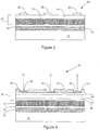
- Figures 2 and 3 illustrate devices that can advantageously be obtained by the disclosed method. Wherever possible, corresponding elements carry the same reference numerals in Figures 2 and 3 as in Figure 1 . Accordingly, Figure 2 illustrates a high-power, high-frequency wide bandgap device broadly designated at 20 that exhibits reduced junction temperature and higher power density during operation and improved reliability at a rated power density.
- the structure comprises a diamond substrate 11 for providing a heat sink with a thermal conductivity greater than silicon carbide, and that will thus carry off more heat than an equivalent amount of SiC.
- a single crystal silicon carbide layer 10 is on the diamond substrate 11 for providing a crystal lattice match for wide bandgap material structures that is better than the crystal match of diamond.
- a Group III nitride heterostructure indicated by the brackets 21 is on the single crystal silicon carbide layer for providing device characteristics.
- Figure 2 also illustrates the aluminum nitride buffer layer 16 which is preferably incorporated into the structure.
- the heterostructure 21 is in its most basic format formed of two different layers of Group III nitride such as the aluminum gallium nitride layer 14 and the gallium nitride layer 15.
- Group III nitride such as the aluminum gallium nitride layer 14 and the gallium nitride layer 15.
- Figures 2 and 3 are schematic in nature and that more complex structures can be incorporated as desired or necessary, including double heterojunctions, barrier HEMTs, multiple quantum wells (MQWs), and superlattice structures.
- MQWs multiple quantum wells
- superlattice structures it will likewise be understood that when the singular term "layer” is used to describe portions of a Group III nitride device, it can include multiple layers that are commonly included in such devices for both manufacturing and operational purposes.
- the ternary Compounds such as AlGaN are more descriptively expressed as Al x Ga 1-x N where 0 ⁇ x ⁇ 1 and that the respective mole fractions of aluminum and gallium (as expressed by x and 1-x) can be adjusted to provide desired or necessary properties.
- the tertiary Group III nitrides can be expressed in the same manner; e.g. In x Al y Ga 1-x-y N where 0 ⁇ x+y ⁇ 1. Layers, junctions and devices formed of any of these materials can take advantage of the benefits offered by the present invention.
- the diamond substrate 11 can be polycrystalline as this generally provides for less complex and less demanding manufacturing and thus helps increase manufacturing efficiency and reduce manufacturing costs.
- the silicon carbide layer 10 is semi-insulating and if necessary depending upon the overall characteristics, the diamond substrate 11 may be semi-insulating as well.
- the nature and use of semi-insulating silicon carbide is set forth in exemplary (but not limiting) fashion in commonly assigned U.S. Patents Nos. 6,218,680 ; 6,403,982 ; 6,396,080 ; 6,639,247 and 6,507,046 .
- the silicon carbide typically has a polytype selected from the 3C, 4H, 6H and 15R polytypes of silicon carbide as these are the most widely available and suitable for electronic devices. Suitable substrates are commercially available from Cree, Inc. of Durham, NC (www.cree.com).
- a field effect transistor By adding the ohmic contacts 24 and 26 and the Schottky contact 25 to the heterostructure 21 ( Figure 2 ), a field effect transistor can be produced.
- a high frequency high electron mobility transistor HEMT
- the device can be advantageously packaged in (i.e., with or adjacent) a high thermal conductivity material.
- the term "package" is used in its usual sense to refer to the container or structure in which an individual semiconductor device is contained for purposes of incorporating it into a larger circuit or an end use device.
- the package can further include or be formed of diamond as may be desired or necessary to minimize or eliminate stress from materials that are mis-matched in their thermal expansion and to take full advantage of the thermal conductivity of the device.
- the channels of HEMTs and related devices tend to generate the most heat during operation, particularly in the gate region.
- the invention is particularly helpful in both spreading heat from the channel and also acting as a heat sink.
- FIG. 3 illustrates a high electron mobility transistor (HEMT) in somewhat more detail and broadly designated at 30.
- the transistor 30 is formed of a diamond substrate 11 for providing the heat sink (or spreader) as discussed above.
- a semi-insulating layer of silicon carbide 10 is on the diamond substrate 11 for providing a favorable crystal growth surface for the Group III nitride epilayers.
- the heterostructure is formed of a first epitaxial layer 15 on the buffer 16 and a second epitaxial layer (or layers) indicated by the brackets 31 on the first epitaxial layer 15 for forming a heterojunction between the epilayers 15 and 31.
- the Group III nitride of the second epilayer 31 has a wider bandgap than the first Group III nitride of the first epilayer 15 for generating a two-dimensional electron gas (2DEG) in the first epilayer at the interface of the first and second epilayers 15 and 31.
- Respective source 34, gate 35 and drain 36 contacts provide a flow of the electrons between the source 34 and the drain 36 that is controlled by a voltage applied to the gate contact 35.
- the first epitaxial layer 15 comprises gallium nitride and the second epitaxial layer 31 comprises aluminum gallium nitride. More preferably, the gallium nitride layer 15 is undoped and the aluminum gallium nitride layer 31 is doped n-type, for example with silicon (Si). As further illustrated in Figure 3 , the second epitaxial layer 31 includes two, and preferably three layers of aluminum gallium nitride that are respectively illustrated at 40, 41 and 42.
- the second epitaxial layer 31 comprises a doped layer 41 of aluminum gallium nitride and an undoped layer 40 of aluminum gallium nitride with the undoped layer 40 being adjacent the undoped layer 15 of gallium nitride.
- another undoped layer 42 of AlGaN is provided on top of the doped AlGaN layer 41. This structure is set forth and described in U.S. Patent No. 6,583,454 .
- the use of an undoped layer of aluminum gallium nitride between the gallium nitride layer and the doped aluminum gallium nitride layer is referred to as a modulation-doped heterostructure and increases the mobility of electrons in the two-dimensional electron gas by physically separating the dopant in the aluminum gallium nitride layer from the undoped gallium nitride layer.
- the transistor 30 operates more efficiently when a passivation layer 43 is included above the heterostructure formed by the layers 15 and 31.
- the passivation material can be silicon dioxide (SiO 2 ) or silicon nitride (Si 3 N 4 ) provided that it has the relevant passivating characteristics.
- the transistor can also incorporate a barrier layer for reducing gate leakage in the resulting device; or other layers (e.g. layers that improve the performance of the contact to p-type materials) for desired purposes, all while taking advantage of the present invention.
- the transistor 30 of Figure 3 can be packaged in a high thermal conductivity material, potentially including a diamond or diamond-containing package.
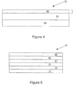
- Such other devices can include lasers, one of which is schematically illustrated in Figure 5 at 45.
- the general theory and operation of semiconductor lasers is well understood by those of appropriate ("ordinary") skill in this art and need not be discussed in detail herein other than to note that the laser is typically formed of an active layer 46, bordered by respective clad layers 47 and 50.
- the nature of the materials for the clad layers particularly their bandgaps and refractive indices are preferably selected so that the active layer forms a potential well between the clad layers.
- the refractive indexes of the clad layers 47 and 50 are preferably such that they encourage the light to remain confined in the active layer for resonance purposes.
- the diamond substrate is illustrated at 11 and the silicon carbide layer at 10 with an appropriate buffer layer 16 included as necessary.
- lasers and light emitting diodes are more likely to include more complex structures such as multiple quantum wells and superlattice structures.
- Figure 4 is a schematic view of a wafer precursor.
- the wafer precursor is broadly designated at 52 and is included herein because the availability of large single crystal substrate wafers in silicon carbide i.e., those of 2-inch, 3-inch, or 100 mm diameter (or equivalent metric sizes) likewise provide the previously unavailable opportunity to, using the method of the invention, obtain diamond layers of this size for the heat sink purposes described herein.
- the disclosed method involves a substrate of single crystal silicon carbide 53 that is at least 2 inches in diameter.
- a layer of diamond 54 is on one face of the silicon carbide substrate 53 and a Group III nitride active structure designated by the brackets 55 is on the opposite face of the wafer 53.
- the substrate silicon carbide wafer 53 is preferably at least about 2 inches (5 centimeters (cm)) in diameter, more preferably at least 3 inches (7.5 cm) in diameter, and most preferably at least 4 inches (10 cm) in diameter.
- the Group III nitride active structure 55 includes at least one heterostructure and the wafer precursor 52 can also include an appropriate buffer layer between the silicon carbide substrate and between the substrate and the heterostructure 55.
- the buffer layer it is not separately illustrated in Figure 4 .
- the silicon carbide can have a polytype selected from the group consisting of the 3C, 4H, 6H, and 15R polytypes of silicon carbide.
- the wafer includes a plurality of individual active structures on the silicon carbide substrate.
- the disclosure has been primarily described herein with respect to the use of diamond as the heat sink material and silicon carbide as the substrate material.
- the disclosure can be understood in a broader aspect, however, in which a layer of higher thermal conductivity material is used in conjunction with a lower thermal conductivity material that has a better crystal lattice match with the Group III nitrides to produce a resulting composite wafer.
- the higher thermal conductivity materials can include metals and semiconductors such as boron nitride (BN), particularly cubic boron nitride (“cBN"), while the more preferred crystal substrate material can be selected from the group consisting of silicon, gallium nitride, aluminum nitride, aluminum gallium nitride, magnesium oxide (MgO), magnesium aluminate (MgAl 2 O 4 ), lithium gallate (LiGaO 2 ), lithium aluminate (LiAlO 2 ), zinc oxide (ZnO), nickel aluminate (NiAl 2 O 4 ), and sapphire, with AlGaN being more preferred.
- the presence of the higher thermal conductivity material as part of the substrate wafer favorably increases the thermal conductivity of the resulting composite wafer.
- Cubic boron nitride (“cBN”) is expected to have advantages in terms of its capability to be made semi-insulating, and for being processed for purposes of the invention in a manner similar to diamond. Boron nitride also has a higher thermal conductivity (13 W/cm-K) than silicon carbide.
- a metal heat sink can be advantageous for reflection and light-extraction purposes.
- Suitable candidate metals can include Ni, Cr, Mn, W, Pt and relevant alloys of these metals. As noted above with respect to the diamond heat sink, the use of any one or more of these metals or alloys should be consistent with the overall manufacture, structure, and operation of the resulting device.
- the method of forming a device in such a composite wafer comprises reducing the thickness of the lower thermal conductivity portion of the composite wafer while retaining a sufficient thickness of the lower thermal conductivity portion to support the desired epitaxial growth thereon.
- the lower thermal conductivity surface is also prepared for epitaxial growth after which an appropriate Group III nitride epilayer, and typically a heterostructure, is added to the prepared face of the lower thermal conductivity portion of the wafer.
Landscapes
- Engineering & Computer Science (AREA)
- Microelectronics & Electronic Packaging (AREA)
- Condensed Matter Physics & Semiconductors (AREA)
- General Physics & Mathematics (AREA)
- Manufacturing & Machinery (AREA)
- Computer Hardware Design (AREA)
- Physics & Mathematics (AREA)
- Power Engineering (AREA)
- Chemical & Material Sciences (AREA)
- Materials Engineering (AREA)
- Junction Field-Effect Transistors (AREA)
- Recrystallisation Techniques (AREA)
- Semiconductor Lasers (AREA)
- Crystals, And After-Treatments Of Crystals (AREA)
Applications Claiming Priority (3)
| Application Number | Priority Date | Filing Date | Title |
|---|---|---|---|
| US10/707,898 US7033912B2 (en) | 2004-01-22 | 2004-01-22 | Silicon carbide on diamond substrates and related devices and methods |
| PCT/US2005/002221 WO2005074013A2 (en) | 2004-01-22 | 2005-01-14 | Silicon carbide on diamond substrates and related devices and methods |
| EP05706059.2A EP1706895B1 (en) | 2004-01-22 | 2005-01-14 | Method for forming a composite substrate for a high power device in wide bandgap materials |
Related Parent Applications (2)
| Application Number | Title | Priority Date | Filing Date |
|---|---|---|---|
| EP05706059.2A Division-Into EP1706895B1 (en) | 2004-01-22 | 2005-01-14 | Method for forming a composite substrate for a high power device in wide bandgap materials |
| EP05706059.2A Division EP1706895B1 (en) | 2004-01-22 | 2005-01-14 | Method for forming a composite substrate for a high power device in wide bandgap materials |
Publications (2)
| Publication Number | Publication Date |
|---|---|
| EP3496152A1 EP3496152A1 (en) | 2019-06-12 |
| EP3496152B1 true EP3496152B1 (en) | 2021-03-31 |
Family
ID=34794562
Family Applications (2)
| Application Number | Title | Priority Date | Filing Date |
|---|---|---|---|
| EP05706059.2A Expired - Lifetime EP1706895B1 (en) | 2004-01-22 | 2005-01-14 | Method for forming a composite substrate for a high power device in wide bandgap materials |
| EP18212254.9A Expired - Lifetime EP3496152B1 (en) | 2004-01-22 | 2005-01-14 | Wide bandgap high electron mobility transistor (hemt) |
Family Applications Before (1)
| Application Number | Title | Priority Date | Filing Date |
|---|---|---|---|
| EP05706059.2A Expired - Lifetime EP1706895B1 (en) | 2004-01-22 | 2005-01-14 | Method for forming a composite substrate for a high power device in wide bandgap materials |
Country Status (8)
| Country | Link |
|---|---|
| US (5) | US7033912B2 (enExample) |
| EP (2) | EP1706895B1 (enExample) |
| JP (2) | JP5192152B2 (enExample) |
| KR (1) | KR20060127907A (enExample) |
| CN (1) | CN100530544C (enExample) |
| CA (1) | CA2554003A1 (enExample) |
| TW (1) | TW200537564A (enExample) |
| WO (1) | WO2005074013A2 (enExample) |
Families Citing this family (105)
| Publication number | Priority date | Publication date | Assignee | Title |
|---|---|---|---|---|
| US7023024B2 (en) * | 2003-03-31 | 2006-04-04 | Inphot, Inc. | Diamond based blue/UV emission source |
| EP1668688A4 (en) | 2003-09-19 | 2011-03-02 | Tinggi Technologies Private Ltd | Fabrication of semiconductor devices |
| US7033912B2 (en) * | 2004-01-22 | 2006-04-25 | Cree, Inc. | Silicon carbide on diamond substrates and related devices and methods |
| US7612390B2 (en) * | 2004-02-05 | 2009-11-03 | Cree, Inc. | Heterojunction transistors including energy barriers |
| ATE533187T1 (de) * | 2004-03-15 | 2011-11-15 | Tinggi Technologies Private Ltd | Fabrikation von halbleiterbauelementen |
| KR20070028364A (ko) | 2004-04-07 | 2007-03-12 | 팅기 테크놀러지스 프라이빗 리미티드 | 반도체 발광 다이오드상의 반사층 제조 |
| US20060073621A1 (en) * | 2004-10-01 | 2006-04-06 | Palo Alto Research Center Incorporated | Group III-nitride based HEMT device with insulating GaN/AlGaN buffer layer |
| US7314520B2 (en) | 2004-10-04 | 2008-01-01 | Cree, Inc. | Low 1c screw dislocation 3 inch silicon carbide wafer |
| US7713839B2 (en) * | 2004-10-06 | 2010-05-11 | Intel Corporation | Diamond substrate formation for electronic assemblies |
| JP4866007B2 (ja) * | 2005-01-14 | 2012-02-01 | 富士通株式会社 | 化合物半導体装置 |
| GB0505752D0 (en) | 2005-03-21 | 2005-04-27 | Element Six Ltd | Diamond based substrate for gan devices |
| KR100609117B1 (ko) * | 2005-05-03 | 2006-08-08 | 삼성전기주식회사 | 질화물계 반도체 발광소자 및 그 제조방법 |
| US7749863B1 (en) * | 2005-05-12 | 2010-07-06 | Hrl Laboratories, Llc | Thermal management substrates |
| US7405430B2 (en) * | 2005-06-10 | 2008-07-29 | Cree, Inc. | Highly uniform group III nitride epitaxial layers on 100 millimeter diameter silicon carbide substrates |
| US9331192B2 (en) * | 2005-06-29 | 2016-05-03 | Cree, Inc. | Low dislocation density group III nitride layers on silicon carbide substrates and methods of making the same |
| US7166485B1 (en) * | 2005-07-05 | 2007-01-23 | Sharp Laboratories Of America, Inc. | Superlattice nanocrystal Si-SiO2 electroluminescence device |
| US20070018198A1 (en) * | 2005-07-20 | 2007-01-25 | Brandes George R | High electron mobility electronic device structures comprising native substrates and methods for making the same |
| US7470958B2 (en) * | 2005-07-28 | 2008-12-30 | Panasonic Corporation | Semiconductor device |
| SG130975A1 (en) * | 2005-09-29 | 2007-04-26 | Tinggi Tech Private Ltd | Fabrication of semiconductor devices for light emission |
| SG131803A1 (en) * | 2005-10-19 | 2007-05-28 | Tinggi Tech Private Ltd | Fabrication of transistors |
| SG133432A1 (en) * | 2005-12-20 | 2007-07-30 | Tinggi Tech Private Ltd | Localized annealing during semiconductor device fabrication |
| US7592211B2 (en) | 2006-01-17 | 2009-09-22 | Cree, Inc. | Methods of fabricating transistors including supported gate electrodes |
| US7709269B2 (en) | 2006-01-17 | 2010-05-04 | Cree, Inc. | Methods of fabricating transistors including dielectrically-supported gate electrodes |
| JP4705482B2 (ja) * | 2006-01-27 | 2011-06-22 | パナソニック株式会社 | トランジスタ |
| US20080292528A1 (en) * | 2006-04-07 | 2008-11-27 | Faris Sadeg M | Methods of and systems for forming carbon based materials |
| JP5274245B2 (ja) * | 2006-04-10 | 2013-08-28 | 富士通株式会社 | 化合物半導体構造とその製造方法 |
| SG140473A1 (en) | 2006-08-16 | 2008-03-28 | Tinggi Tech Private Ltd | Improvements in external light efficiency of light emitting diodes |
| SG140512A1 (en) * | 2006-09-04 | 2008-03-28 | Tinggi Tech Private Ltd | Electrical current distribution in light emitting devices |
| US8823057B2 (en) | 2006-11-06 | 2014-09-02 | Cree, Inc. | Semiconductor devices including implanted regions for providing low-resistance contact to buried layers and related devices |
| JP5725713B2 (ja) * | 2007-01-22 | 2015-05-27 | ダイアモンド マイクロウェーブ デバイセズ リミテッド | 表面を含むダイヤモンド電子デバイス及びそれらの製造方法 |
| US8309967B2 (en) | 2007-05-31 | 2012-11-13 | Chien-Min Sung | Diamond LED devices and associated methods |
| US7781256B2 (en) * | 2007-05-31 | 2010-08-24 | Chien-Min Sung | Semiconductor-on-diamond devices and associated methods |
| US7646025B1 (en) * | 2007-05-31 | 2010-01-12 | Chien-Min Sung | Diamond LED devices and associated methods |
| US7799600B2 (en) * | 2007-05-31 | 2010-09-21 | Chien-Min Sung | Doped diamond LED devices and associated methods |
| US8110846B2 (en) * | 2007-05-31 | 2012-02-07 | Chien-Min Sung | Diamond semiconductor devices and associated methods |
| US7791188B2 (en) | 2007-06-18 | 2010-09-07 | Chien-Min Sung | Heat spreader having single layer of diamond particles and associated methods |
| US20090075455A1 (en) * | 2007-09-14 | 2009-03-19 | Umesh Mishra | Growing N-polar III-nitride Structures |
| US8490678B2 (en) * | 2008-06-02 | 2013-07-23 | Gerald Ho Kim | Silicon-based thermal energy transfer device and apparatus |
| JP5115735B2 (ja) * | 2008-09-04 | 2013-01-09 | 富士電機株式会社 | 炭化珪素半導体基板とその製造方法 |
| US7888171B2 (en) * | 2008-12-22 | 2011-02-15 | Raytheon Company | Fabricating a gallium nitride layer with diamond layers |
| US20110108854A1 (en) * | 2009-11-10 | 2011-05-12 | Chien-Min Sung | Substantially lattice matched semiconductor materials and associated methods |
| US20110140232A1 (en) * | 2009-12-15 | 2011-06-16 | Intersil Americas Inc. | Methods of forming a thermal conduction region in a semiconductor structure and structures resulting therefrom |
| US20110180855A1 (en) * | 2010-01-28 | 2011-07-28 | Gm Global Technology Operations, Inc. | Non-direct bond copper isolated lateral wide band gap semiconductor device |
| WO2011132285A1 (ja) * | 2010-04-22 | 2011-10-27 | 三菱電機株式会社 | 半導体装置およびその製造方法 |
| JP5598542B2 (ja) * | 2010-05-10 | 2014-10-01 | 三菱電機株式会社 | 炭化珪素エピタキシャルウエハ及びその製造方法並びにエピタキシャル成長用炭化珪素バルク基板及びその製造方法 |
| GB201010705D0 (en) * | 2010-06-25 | 2010-08-11 | Element Six Ltd | Substrates for semiconductor devices |
| KR101834802B1 (ko) * | 2011-09-01 | 2018-04-13 | 엘지이노텍 주식회사 | 반도체 소자 |
| JP5546514B2 (ja) * | 2011-09-20 | 2014-07-09 | 古河電気工業株式会社 | 窒化物半導体素子及び製造方法 |
| US8884308B2 (en) | 2011-11-29 | 2014-11-11 | Taiwan Semiconductor Manufacturing Company, Ltd. | High electron mobility transistor structure with improved breakdown voltage performance |
| GB201121655D0 (en) | 2011-12-16 | 2012-01-25 | Element Six Ltd | Substrates for semiconductor devices |
| GB201121659D0 (en) | 2011-12-16 | 2012-01-25 | Element Six Ltd | Substrates for semiconductor devices |
| GB201121666D0 (en) | 2011-12-16 | 2012-01-25 | Element Six Ltd | Synthetic diamond coated compound semiconductor substrates |
| US8614447B2 (en) * | 2012-01-30 | 2013-12-24 | International Business Machines Corporation | Semiconductor substrates using bandgap material between III-V channel material and insulator layer |
| US9359693B2 (en) | 2012-02-29 | 2016-06-07 | Element Six Technologies Us Corporation | Gallium-nitride-on-diamond wafers and manufacturing equipment and methods of manufacture |
| US8575657B2 (en) | 2012-03-20 | 2013-11-05 | Northrop Grumman Systems Corporation | Direct growth of diamond in backside vias for GaN HEMT devices |
| US9496197B1 (en) | 2012-04-20 | 2016-11-15 | Hrl Laboratories, Llc | Near junction cooling for GaN devices |
| JP5343224B1 (ja) * | 2012-09-28 | 2013-11-13 | Roca株式会社 | 半導体装置および結晶 |
| EP2912685B1 (en) | 2012-10-26 | 2020-04-08 | RFHIC Corporation | Semiconductor devices with improved reliability and operating life and methods of manufacturing the same |
| EP2936550B1 (en) | 2012-12-18 | 2021-05-19 | RFHIC Corporation | Substrates for semiconductor devices |
| TWI506788B (zh) | 2012-12-25 | 2015-11-01 | Huga Optotech Inc | 場效電晶體 |
| JP2014127707A (ja) * | 2012-12-27 | 2014-07-07 | Toshiba Corp | 電子部品 |
| US10322936B2 (en) | 2013-05-02 | 2019-06-18 | Pallidus, Inc. | High purity polysilocarb materials, applications and processes |
| US9919972B2 (en) | 2013-05-02 | 2018-03-20 | Melior Innovations, Inc. | Pressed and self sintered polymer derived SiC materials, applications and devices |
| US11091370B2 (en) | 2013-05-02 | 2021-08-17 | Pallidus, Inc. | Polysilocarb based silicon carbide materials, applications and devices |
| US9657409B2 (en) | 2013-05-02 | 2017-05-23 | Melior Innovations, Inc. | High purity SiOC and SiC, methods compositions and applications |
| RU2534442C1 (ru) * | 2013-07-04 | 2014-11-27 | Открытое акционерное общество "Научно-производственное предприятие "Пульсар" | Способ изготовления мощного свч-транзистора |
| US9196703B2 (en) * | 2013-08-22 | 2015-11-24 | Northrop Grumman Systems Corporation | Selective deposition of diamond in thermal vias |
| DE102015103323A1 (de) * | 2015-03-06 | 2016-09-08 | Infineon Technologies Austria Ag | Verfahren zum Herstellen von Halbleitervorrichtungen durch Bonden einer Halbleiterscheibe auf ein Basissubstrat, zusammengesetzter Wafer und Halbleitervorrichtung |
| US9406536B1 (en) * | 2015-06-29 | 2016-08-02 | Hermes-Epitek Corp. | Method and system for manufacturing semiconductor epitaxy structure |
| CN105322007B (zh) * | 2015-07-20 | 2018-12-28 | 苏州能讯高能半导体有限公司 | 基于金刚石衬底的氮化物结构、制备方法及半导体器件 |
| US10584412B2 (en) | 2016-03-08 | 2020-03-10 | Ii-Vi Delaware, Inc. | Substrate comprising a layer of silicon and a layer of diamond having an optically finished (or a dense) silicon-diamond interface |
| JP6735588B2 (ja) * | 2016-03-30 | 2020-08-05 | 株式会社サイオクス | 窒化物半導体テンプレート、窒化物半導体積層物、窒化物半導体テンプレートの製造方法、および窒化物半導体積層物の製造方法 |
| JP6868389B2 (ja) * | 2016-12-27 | 2021-05-12 | 住友化学株式会社 | 半導体基板および電子デバイス |
| JP6819318B2 (ja) * | 2017-01-25 | 2021-01-27 | 富士通株式会社 | 半導体装置、半導体集積回路及び半導体装置の製造方法 |
| US10332820B2 (en) | 2017-03-20 | 2019-06-25 | Akash Systems, Inc. | Satellite communication transmitter with improved thermal management |
| KR20250113525A (ko) | 2017-03-29 | 2025-07-25 | 팔리두스, 인크. | SiC 용적측정 형태 및 보올을 형성하는 방법 |
| CN107039373A (zh) * | 2017-05-31 | 2017-08-11 | 母凤文 | 氮化镓器件结构及其制备方法 |
| US10374553B2 (en) | 2017-06-15 | 2019-08-06 | Akash Systems, Inc. | Microwave transmitter with improved information throughput |
| US10692752B2 (en) | 2017-06-20 | 2020-06-23 | Elta Systems Ltd. | Gallium nitride semiconductor structure and process for fabricating thereof |
| IL253085B (en) * | 2017-06-20 | 2021-06-30 | Elta Systems Ltd | Gallium nitride semiconductor structure and process for its production |
| US10128107B1 (en) * | 2017-08-31 | 2018-11-13 | Rfhic Corporation | Wafers having III-Nitride and diamond layers |
| CN110828293A (zh) * | 2018-08-13 | 2020-02-21 | 西安电子科技大学 | 基于SiC/金刚石复合衬底层的半导体器件及其制备方法 |
| CN110828292A (zh) * | 2018-08-13 | 2020-02-21 | 西安电子科技大学 | 基于复合衬底的半导体器件及其制备方法 |
| JP7172556B2 (ja) * | 2018-12-19 | 2022-11-16 | 株式会社Sumco | 多結晶ダイヤモンド自立基板の製造方法 |
| CN109830457B (zh) * | 2019-02-15 | 2021-02-23 | 长江存储科技有限责任公司 | 半导体器件及其形成方法 |
| CN112436056B (zh) * | 2019-08-26 | 2024-03-26 | 联华电子股份有限公司 | 高电子迁移率晶体管 |
| DE102019122888B4 (de) * | 2019-08-27 | 2024-09-26 | Infineon Technologies Ag | Leistungshalbleitervorrichtung und Verfahren |
| CN112786449A (zh) * | 2019-11-07 | 2021-05-11 | 上海华为技术有限公司 | Hemt器件制造方法、hemt器件及射频功率放大器 |
| JP7382804B2 (ja) * | 2019-11-22 | 2023-11-17 | 三菱電機株式会社 | 半導体装置、半導体装置の製造方法、及び、電界効果型トランジスタ |
| US11652146B2 (en) | 2020-02-07 | 2023-05-16 | Rfhic Corporation | Method of forming a semiconductor wafer containing a gallium-nitride layer and two diamond layers |
| KR102273305B1 (ko) * | 2020-04-23 | 2021-07-06 | 알에프에이치아이씨 주식회사 | 신뢰성을 개선한 다이아몬드 기판 상 질화 갈륨 반도체 구조체 및 이를 제조하는 공정 |
| CN111640828B (zh) * | 2020-06-18 | 2021-08-31 | 佛山紫熙慧众科技有限公司 | AlGaN基紫外LED外延结构 |
| WO2022019799A1 (ru) * | 2020-07-24 | 2022-01-27 | Общество С Ограниченной Ответственностью "Вандер Технолоджис" | Гетероэпитаксиальная структура с алмазным теплоотводом |
| TWI745110B (zh) * | 2020-10-06 | 2021-11-01 | 環球晶圓股份有限公司 | 半導體基板及其製造方法 |
| FR3114912B1 (fr) * | 2020-10-06 | 2022-09-02 | Soitec Silicon On Insulator | Procédé de fabrication d’un substrat pour la croissance épitaxiale d’une couche d’un alliage III-N à base de gallium |
| TWI846108B (zh) * | 2022-10-24 | 2024-06-21 | 國立成功大學 | 磊晶薄膜的製造方法與磊晶薄膜 |
| US12191227B2 (en) | 2020-12-14 | 2025-01-07 | Electronics And Telecommunications Research Institute | Heat dissipating substrate comprising diamond and semiconductor integrated device including the same |
| CN112993042A (zh) * | 2021-02-05 | 2021-06-18 | 中国电子科技集团公司第十三研究所 | 倍频单片、GaN太赫兹二极管及其制备方法 |
| WO2023048160A1 (ja) * | 2021-09-22 | 2023-03-30 | エア・ウォーター株式会社 | 半導体基板、半導体デバイス、半導体基板の製造方法、および半導体デバイスの製造方法 |
| CN114530366B (zh) * | 2022-01-05 | 2025-08-26 | 西安电子科技大学 | 采用低温脉冲层在金刚石上外延β-Ga2O3薄膜的制备方法及结构 |
| CN114804930A (zh) * | 2022-04-18 | 2022-07-29 | 苏州博志金钻科技有限责任公司 | 一种高功率半导体器件散热用单晶碳化硅金属化复合陶瓷片 |
| CN115863400B (zh) * | 2023-02-24 | 2023-05-16 | 成都功成半导体有限公司 | 一种高导热GaN基HEMT器件及其制备方法 |
| CN118824845B (zh) * | 2024-09-18 | 2024-11-22 | 山东大学 | 一种碳化硅功率器件及其制备方法和应用 |
| CN119113918B (zh) * | 2024-09-20 | 2025-09-16 | 焦作天宝桓祥机械科技有限公司 | 一种以碳化硅晶圆制备金刚石晶圆的方法 |
| CN119517182B (zh) * | 2024-10-30 | 2025-11-18 | 武汉大学深圳研究院 | 一种改善金刚石衬底异质外延生长氮化镓的仿真方法 |
Family Cites Families (67)
| Publication number | Priority date | Publication date | Assignee | Title |
|---|---|---|---|---|
| US654833A (en) * | 1898-07-20 | 1900-07-31 | Edward W Jenkins | Grain-binder. |
| US2938136A (en) | 1958-08-26 | 1960-05-24 | Gen Electric | Electroluminescent lamp |
| US5373171A (en) | 1987-03-12 | 1994-12-13 | Sumitomo Electric Industries, Ltd. | Thin film single crystal substrate |
| US5030583A (en) | 1988-12-02 | 1991-07-09 | Advanced Technolgy Materials, Inc. | Method of making single crystal semiconductor substrate articles and semiconductor device |
| US5006914A (en) | 1988-12-02 | 1991-04-09 | Advanced Technology Materials, Inc. | Single crystal semiconductor substrate articles and semiconductor devices comprising same |
| US5210051A (en) | 1990-03-27 | 1993-05-11 | Cree Research, Inc. | High efficiency light emitting diodes from bipolar gallium nitride |
| JPH03295267A (ja) | 1990-04-13 | 1991-12-26 | Seiko Epson Corp | 薄膜装置 |
| JPH04192552A (ja) * | 1990-11-27 | 1992-07-10 | Nec Corp | 半導体素子用パッケージ |
| US5311055A (en) | 1991-11-22 | 1994-05-10 | The United States Of America As Represented By The Secretary Of The Navy | Trenched bipolar transistor structures |
| DE4323814A1 (de) | 1992-09-25 | 1994-03-31 | Siemens Ag | MIS-Feldeffekttransistor |
| US5422901A (en) | 1993-11-15 | 1995-06-06 | Motorola, Inc. | Semiconductor device with high heat conductivity |
| US5393993A (en) | 1993-12-13 | 1995-02-28 | Cree Research, Inc. | Buffer structure between silicon carbide and gallium nitride and resulting semiconductor devices |
| US5679152A (en) | 1994-01-27 | 1997-10-21 | Advanced Technology Materials, Inc. | Method of making a single crystals Ga*N article |
| US5523589A (en) | 1994-09-20 | 1996-06-04 | Cree Research, Inc. | Vertical geometry light emitting diode with group III nitride active layer and extended lifetime |
| JP3295267B2 (ja) | 1995-03-24 | 2002-06-24 | 株式会社クボタ | ディーゼルエンジンの副室式燃焼室 |
| US5661312A (en) | 1995-03-30 | 1997-08-26 | Motorola | Silicon carbide MOSFET |
| US5803967A (en) * | 1995-05-31 | 1998-09-08 | Kobe Steel Usa Inc. | Method of forming diamond devices having textured and highly oriented diamond layers therein |
| US6670693B1 (en) | 1996-12-05 | 2003-12-30 | Nathaniel R. Quick | Laser synthesized wide-bandgap semiconductor electronic devices and circuits |
| JP3508356B2 (ja) * | 1995-12-25 | 2004-03-22 | 松下電器産業株式会社 | 半導体結晶成長方法及び半導体薄膜 |
| JP3344205B2 (ja) * | 1996-03-28 | 2002-11-11 | 信越半導体株式会社 | シリコンウェーハの製造方法及びシリコンウェーハ |
| US5872415A (en) | 1996-08-16 | 1999-02-16 | Kobe Steel Usa Inc. | Microelectronic structures including semiconductor islands |
| JP3951324B2 (ja) * | 1996-09-03 | 2007-08-01 | 住友電気工業株式会社 | 気相合成ダイヤモンドおよびその製造方法 |
| US6533874B1 (en) | 1996-12-03 | 2003-03-18 | Advanced Technology Materials, Inc. | GaN-based devices using thick (Ga, Al, In)N base layers |
| JPH10294452A (ja) * | 1997-04-22 | 1998-11-04 | Sony Corp | ヘテロ接合電界効果トランジスタ |
| US6150239A (en) | 1997-05-31 | 2000-11-21 | Max Planck Society | Method for the transfer of thin layers monocrystalline material onto a desirable substrate |
| DE19808069A1 (de) | 1998-02-26 | 1999-09-02 | Bosch Gmbh Robert | Verfahren zum Fixieren einer Rotorwicklung |
| US6396864B1 (en) | 1998-03-13 | 2002-05-28 | Jds Uniphase Corporation | Thermally conductive coatings for light emitting devices |
| US6316793B1 (en) | 1998-06-12 | 2001-11-13 | Cree, Inc. | Nitride based transistors on semi-insulating silicon carbide substrates |
| JP3144387B2 (ja) * | 1998-08-17 | 2001-03-12 | 日本電気株式会社 | 半導体装置の製造方法 |
| JP2000174166A (ja) * | 1998-10-02 | 2000-06-23 | Sumitomo Electric Ind Ltd | 半導体搭載パッケ―ジ |
| GB2343091B (en) * | 1998-10-19 | 2004-05-19 | Ibm | Electronic business card exchange |
| US6744800B1 (en) | 1998-12-30 | 2004-06-01 | Xerox Corporation | Method and structure for nitride based laser diode arrays on an insulating substrate |
| US6396080B2 (en) | 1999-05-18 | 2002-05-28 | Cree, Inc | Semi-insulating silicon carbide without vanadium domination |
| US6218680B1 (en) | 1999-05-18 | 2001-04-17 | Cree, Inc. | Semi-insulating silicon carbide without vanadium domination |
| US6255712B1 (en) * | 1999-08-14 | 2001-07-03 | International Business Machines Corporation | Semi-sacrificial diamond for air dielectric formation |
| US6448642B1 (en) | 2000-01-27 | 2002-09-10 | William W. Bewley | Pressure-bonded heat-sink system |
| US6586781B2 (en) | 2000-02-04 | 2003-07-01 | Cree Lighting Company | Group III nitride based FETs and HEMTs with reduced trapping and method for producing the same |
| US7205578B2 (en) | 2000-02-15 | 2007-04-17 | Osram Gmbh | Semiconductor component which emits radiation, and method for producing the same |
| DE10032838B4 (de) | 2000-07-06 | 2015-08-20 | Osram Opto Semiconductors Gmbh | Strahlung emittierender Halbleiterchip und Verfahren zu dessen Herstellung |
| JP2002359247A (ja) * | 2000-07-10 | 2002-12-13 | Canon Inc | 半導体部材、半導体装置およびそれらの製造方法 |
| FR2835096B1 (fr) | 2002-01-22 | 2005-02-18 | Procede de fabrication d'un substrat auto-porte en materiau semi-conducteur monocristallin | |
| FR2817395B1 (fr) * | 2000-11-27 | 2003-10-31 | Soitec Silicon On Insulator | Procede de fabrication d'un substrat notamment pour l'optique, l'electronique ou l'optoelectronique et substrat obtenu par ce procede |
| WO2002044444A1 (en) | 2000-11-30 | 2002-06-06 | Kyma Technologies, Inc. | Method and apparatus for producing miiin columns and miiin materials grown thereon |
| US6548333B2 (en) | 2000-12-01 | 2003-04-15 | Cree, Inc. | Aluminum gallium nitride/gallium nitride high electron mobility transistors having a gate contact on a gallium nitride based cap segment |
| JP4554803B2 (ja) | 2000-12-04 | 2010-09-29 | 独立行政法人理化学研究所 | 低転位バッファーおよびその製造方法ならびに低転位バッファーを備えた素子 |
| US6497763B2 (en) | 2001-01-19 | 2002-12-24 | The United States Of America As Represented By The Secretary Of The Navy | Electronic device with composite substrate |
| JP2002220299A (ja) | 2001-01-19 | 2002-08-09 | Hoya Corp | 単結晶SiC及びその製造方法、SiC半導体装置並びにSiC複合材料 |
| US6956250B2 (en) | 2001-02-23 | 2005-10-18 | Nitronex Corporation | Gallium nitride materials including thermally conductive regions |
| US6699770B2 (en) | 2001-03-01 | 2004-03-02 | John Tarje Torvik | Method of making a hybride substrate having a thin silicon carbide membrane layer |
| JP2002265296A (ja) | 2001-03-09 | 2002-09-18 | Kobe Steel Ltd | ダイヤモンド薄膜及びその製造方法 |
| US20030201459A1 (en) * | 2001-03-29 | 2003-10-30 | Sheppard Scott Thomas | Nitride based transistors on semi-insulating silicon carbide substrates |
| US6686676B2 (en) | 2001-04-30 | 2004-02-03 | General Electric Company | UV reflectors and UV-based light sources having reduced UV radiation leakage incorporating the same |
| US6507046B2 (en) | 2001-05-11 | 2003-01-14 | Cree, Inc. | High-resistivity silicon carbide substrate for semiconductor devices with high break down voltage |
| US6849882B2 (en) | 2001-05-11 | 2005-02-01 | Cree Inc. | Group-III nitride based high electron mobility transistor (HEMT) with barrier/spacer layer |
| JP2003037074A (ja) | 2001-07-26 | 2003-02-07 | Toshiba Corp | 半導体装置およびその製造方法 |
| US6770966B2 (en) | 2001-07-31 | 2004-08-03 | Intel Corporation | Electronic assembly including a die having an integrated circuit and a layer of diamond to transfer heat |
| US6634770B2 (en) | 2001-08-24 | 2003-10-21 | Densen Cao | Light source using semiconductor devices mounted on a heat sink |
| AU2002337297A1 (en) | 2001-10-23 | 2003-05-06 | Cambridge Semiconductor Limited | Lateral semiconductor-on-insulator structure and corresponding manufacturing methods |
| US6670283B2 (en) | 2001-11-20 | 2003-12-30 | International Business Machines Corporation | Backside protection films |
| JP4117535B2 (ja) * | 2001-11-30 | 2008-07-16 | 信越半導体株式会社 | 化合物半導体素子 |
| US7030428B2 (en) * | 2001-12-03 | 2006-04-18 | Cree, Inc. | Strain balanced nitride heterojunction transistors |
| JP3812452B2 (ja) * | 2002-02-04 | 2006-08-23 | 松下電器産業株式会社 | ドライエッチング方法 |
| JP4182323B2 (ja) | 2002-02-27 | 2008-11-19 | ソニー株式会社 | 複合基板、基板製造方法 |
| CN1663049A (zh) | 2002-06-26 | 2005-08-31 | 剑桥半导体有限公司 | 横向半导体器件 |
| CN1467862A (zh) * | 2002-07-10 | 2004-01-14 | 洲磊科技股份有限公司 | 具有欧姆接触的半导体装置及其制造方法 |
| US7535100B2 (en) | 2002-07-12 | 2009-05-19 | The United States Of America As Represented By The Secretary Of The Navy | Wafer bonding of thinned electronic materials and circuits to high performance substrates |
| US7033912B2 (en) * | 2004-01-22 | 2006-04-25 | Cree, Inc. | Silicon carbide on diamond substrates and related devices and methods |
-
2004
- 2004-01-22 US US10/707,898 patent/US7033912B2/en not_active Expired - Lifetime
-
2005
- 2005-01-14 JP JP2006551378A patent/JP5192152B2/ja not_active Expired - Lifetime
- 2005-01-14 EP EP05706059.2A patent/EP1706895B1/en not_active Expired - Lifetime
- 2005-01-14 CN CNB2005800029687A patent/CN100530544C/zh not_active Expired - Lifetime
- 2005-01-14 WO PCT/US2005/002221 patent/WO2005074013A2/en not_active Ceased
- 2005-01-14 KR KR20067014842A patent/KR20060127907A/ko not_active Withdrawn
- 2005-01-14 CA CA 2554003 patent/CA2554003A1/en not_active Abandoned
- 2005-01-14 EP EP18212254.9A patent/EP3496152B1/en not_active Expired - Lifetime
- 2005-01-21 TW TW94101865A patent/TW200537564A/zh unknown
-
2006
- 2006-02-06 US US11/347,953 patent/US7579626B2/en not_active Expired - Lifetime
-
2009
- 2009-07-17 US US12/504,725 patent/US7863624B2/en not_active Expired - Lifetime
-
2010
- 2010-11-23 US US12/952,278 patent/US8513672B2/en not_active Expired - Fee Related
-
2012
- 2012-07-02 JP JP2012148508A patent/JP6227231B2/ja not_active Expired - Lifetime
-
2013
- 2013-07-23 US US13/948,675 patent/US9142617B2/en not_active Expired - Lifetime
Non-Patent Citations (1)
| Title |
|---|
| None * |
Also Published As
| Publication number | Publication date |
|---|---|
| CN100530544C (zh) | 2009-08-19 |
| US8513672B2 (en) | 2013-08-20 |
| JP2012238861A (ja) | 2012-12-06 |
| TW200537564A (en) | 2005-11-16 |
| US20130306990A1 (en) | 2013-11-21 |
| US9142617B2 (en) | 2015-09-22 |
| JP2007519262A (ja) | 2007-07-12 |
| EP1706895B1 (en) | 2019-08-28 |
| JP6227231B2 (ja) | 2017-11-08 |
| US7863624B2 (en) | 2011-01-04 |
| EP1706895A2 (en) | 2006-10-04 |
| US20060138455A1 (en) | 2006-06-29 |
| JP5192152B2 (ja) | 2013-05-08 |
| US20050164482A1 (en) | 2005-07-28 |
| US7579626B2 (en) | 2009-08-25 |
| CN1910737A (zh) | 2007-02-07 |
| US7033912B2 (en) | 2006-04-25 |
| US20110064105A1 (en) | 2011-03-17 |
| CA2554003A1 (en) | 2005-08-11 |
| KR20060127907A (ko) | 2006-12-13 |
| WO2005074013A2 (en) | 2005-08-11 |
| US20090272984A1 (en) | 2009-11-05 |
| EP3496152A1 (en) | 2019-06-12 |
| WO2005074013A3 (en) | 2005-11-03 |
Similar Documents
| Publication | Publication Date | Title |
|---|---|---|
| EP3496152B1 (en) | Wide bandgap high electron mobility transistor (hemt) | |
| CA2447058C (en) | Group-iii nitride based high electron mobility transistor (hemt) with barrier/spacer layer | |
| US9224596B2 (en) | Methods of fabricating thick semi-insulating or insulating epitaxial gallium nitride layers | |
| JP2019186316A (ja) | トランジスタの製造方法 | |
| WO2022049983A1 (ja) | 半導体装置、半導体モジュール、及び無線通信装置 | |
| WO2023129293A1 (en) | Ain channel heterostructure field effect transistor | |
| WO2023276275A1 (ja) | 半導体装置、半導体モジュール、および無線通信装置 | |
| Thuret et al. | Recent Achievement in the GaN Epitaxy on Silicon and Engineering Substrates |
Legal Events
| Date | Code | Title | Description |
|---|---|---|---|
| PUAI | Public reference made under article 153(3) epc to a published international application that has entered the european phase |
Free format text: ORIGINAL CODE: 0009012 |
|
| STAA | Information on the status of an ep patent application or granted ep patent |
Free format text: STATUS: THE APPLICATION HAS BEEN PUBLISHED |
|
| AC | Divisional application: reference to earlier application |
Ref document number: 1706895 Country of ref document: EP Kind code of ref document: P |
|
| AK | Designated contracting states |
Kind code of ref document: A1 Designated state(s): AT BE BG CH CY CZ DE DK EE ES FI FR GB GR HU IE IS IT LI LT LU MC NL PL PT RO SE SI SK TR |
|
| STAA | Information on the status of an ep patent application or granted ep patent |
Free format text: STATUS: REQUEST FOR EXAMINATION WAS MADE |
|
| 17P | Request for examination filed |
Effective date: 20191127 |
|
| RBV | Designated contracting states (corrected) |
Designated state(s): AT BE BG CH CY CZ DE DK EE ES FI FR GB GR HU IE IS IT LI LT LU MC NL PL PT RO SE SI SK TR |
|
| STAA | Information on the status of an ep patent application or granted ep patent |
Free format text: STATUS: EXAMINATION IS IN PROGRESS |
|
| 17Q | First examination report despatched |
Effective date: 20200323 |
|
| GRAP | Despatch of communication of intention to grant a patent |
Free format text: ORIGINAL CODE: EPIDOSNIGR1 |
|
| STAA | Information on the status of an ep patent application or granted ep patent |
Free format text: STATUS: GRANT OF PATENT IS INTENDED |
|
| INTG | Intention to grant announced |
Effective date: 20201105 |
|
| RIN1 | Information on inventor provided before grant (corrected) |
Inventor name: SAXLER, ADAM WILLIAM |
|
| GRAS | Grant fee paid |
Free format text: ORIGINAL CODE: EPIDOSNIGR3 |
|
| GRAA | (expected) grant |
Free format text: ORIGINAL CODE: 0009210 |
|
| STAA | Information on the status of an ep patent application or granted ep patent |
Free format text: STATUS: THE PATENT HAS BEEN GRANTED |
|
| AC | Divisional application: reference to earlier application |
Ref document number: 1706895 Country of ref document: EP Kind code of ref document: P |
|
| AK | Designated contracting states |
Kind code of ref document: B1 Designated state(s): AT BE BG CH CY CZ DE DK EE ES FI FR GB GR HU IE IS IT LI LT LU MC NL PL PT RO SE SI SK TR |
|
| REG | Reference to a national code |
Ref country code: GB Ref legal event code: FG4D Ref country code: CH Ref legal event code: EP |
|
| REG | Reference to a national code |
Ref country code: DE Ref legal event code: R096 Ref document number: 602005057179 Country of ref document: DE Ref country code: AT Ref legal event code: REF Ref document number: 1377921 Country of ref document: AT Kind code of ref document: T Effective date: 20210415 |
|
| REG | Reference to a national code |
Ref country code: IE Ref legal event code: FG4D |
|
| REG | Reference to a national code |
Ref country code: LT Ref legal event code: MG9D |
|
| PG25 | Lapsed in a contracting state [announced via postgrant information from national office to epo] |
Ref country code: BG Free format text: LAPSE BECAUSE OF FAILURE TO SUBMIT A TRANSLATION OF THE DESCRIPTION OR TO PAY THE FEE WITHIN THE PRESCRIBED TIME-LIMIT Effective date: 20210630 Ref country code: FI Free format text: LAPSE BECAUSE OF FAILURE TO SUBMIT A TRANSLATION OF THE DESCRIPTION OR TO PAY THE FEE WITHIN THE PRESCRIBED TIME-LIMIT Effective date: 20210331 |
|
| PG25 | Lapsed in a contracting state [announced via postgrant information from national office to epo] |
Ref country code: SE Free format text: LAPSE BECAUSE OF FAILURE TO SUBMIT A TRANSLATION OF THE DESCRIPTION OR TO PAY THE FEE WITHIN THE PRESCRIBED TIME-LIMIT Effective date: 20210331 |
|
| REG | Reference to a national code |
Ref country code: NL Ref legal event code: MP Effective date: 20210331 |
|
| REG | Reference to a national code |
Ref country code: AT Ref legal event code: MK05 Ref document number: 1377921 Country of ref document: AT Kind code of ref document: T Effective date: 20210331 |
|
| PG25 | Lapsed in a contracting state [announced via postgrant information from national office to epo] |
Ref country code: AT Free format text: LAPSE BECAUSE OF FAILURE TO SUBMIT A TRANSLATION OF THE DESCRIPTION OR TO PAY THE FEE WITHIN THE PRESCRIBED TIME-LIMIT Effective date: 20210331 Ref country code: NL Free format text: LAPSE BECAUSE OF FAILURE TO SUBMIT A TRANSLATION OF THE DESCRIPTION OR TO PAY THE FEE WITHIN THE PRESCRIBED TIME-LIMIT Effective date: 20210331 Ref country code: CZ Free format text: LAPSE BECAUSE OF FAILURE TO SUBMIT A TRANSLATION OF THE DESCRIPTION OR TO PAY THE FEE WITHIN THE PRESCRIBED TIME-LIMIT Effective date: 20210331 Ref country code: EE Free format text: LAPSE BECAUSE OF FAILURE TO SUBMIT A TRANSLATION OF THE DESCRIPTION OR TO PAY THE FEE WITHIN THE PRESCRIBED TIME-LIMIT Effective date: 20210331 Ref country code: LT Free format text: LAPSE BECAUSE OF FAILURE TO SUBMIT A TRANSLATION OF THE DESCRIPTION OR TO PAY THE FEE WITHIN THE PRESCRIBED TIME-LIMIT Effective date: 20210331 |
|
| PG25 | Lapsed in a contracting state [announced via postgrant information from national office to epo] |
Ref country code: IS Free format text: LAPSE BECAUSE OF FAILURE TO SUBMIT A TRANSLATION OF THE DESCRIPTION OR TO PAY THE FEE WITHIN THE PRESCRIBED TIME-LIMIT Effective date: 20210731 Ref country code: PT Free format text: LAPSE BECAUSE OF FAILURE TO SUBMIT A TRANSLATION OF THE DESCRIPTION OR TO PAY THE FEE WITHIN THE PRESCRIBED TIME-LIMIT Effective date: 20210802 Ref country code: PL Free format text: LAPSE BECAUSE OF FAILURE TO SUBMIT A TRANSLATION OF THE DESCRIPTION OR TO PAY THE FEE WITHIN THE PRESCRIBED TIME-LIMIT Effective date: 20210331 Ref country code: RO Free format text: LAPSE BECAUSE OF FAILURE TO SUBMIT A TRANSLATION OF THE DESCRIPTION OR TO PAY THE FEE WITHIN THE PRESCRIBED TIME-LIMIT Effective date: 20210331 Ref country code: SK Free format text: LAPSE BECAUSE OF FAILURE TO SUBMIT A TRANSLATION OF THE DESCRIPTION OR TO PAY THE FEE WITHIN THE PRESCRIBED TIME-LIMIT Effective date: 20210331 |
|
| REG | Reference to a national code |
Ref country code: DE Ref legal event code: R097 Ref document number: 602005057179 Country of ref document: DE |
|
| PG25 | Lapsed in a contracting state [announced via postgrant information from national office to epo] |
Ref country code: ES Free format text: LAPSE BECAUSE OF FAILURE TO SUBMIT A TRANSLATION OF THE DESCRIPTION OR TO PAY THE FEE WITHIN THE PRESCRIBED TIME-LIMIT Effective date: 20210331 Ref country code: DK Free format text: LAPSE BECAUSE OF FAILURE TO SUBMIT A TRANSLATION OF THE DESCRIPTION OR TO PAY THE FEE WITHIN THE PRESCRIBED TIME-LIMIT Effective date: 20210331 |
|
| PLBE | No opposition filed within time limit |
Free format text: ORIGINAL CODE: 0009261 |
|
| STAA | Information on the status of an ep patent application or granted ep patent |
Free format text: STATUS: NO OPPOSITION FILED WITHIN TIME LIMIT |
|
| 26N | No opposition filed |
Effective date: 20220104 |
|
| PG25 | Lapsed in a contracting state [announced via postgrant information from national office to epo] |
Ref country code: IS Free format text: LAPSE BECAUSE OF FAILURE TO SUBMIT A TRANSLATION OF THE DESCRIPTION OR TO PAY THE FEE WITHIN THE PRESCRIBED TIME-LIMIT Effective date: 20210731 |
|
| PG25 | Lapsed in a contracting state [announced via postgrant information from national office to epo] |
Ref country code: IT Free format text: LAPSE BECAUSE OF FAILURE TO SUBMIT A TRANSLATION OF THE DESCRIPTION OR TO PAY THE FEE WITHIN THE PRESCRIBED TIME-LIMIT Effective date: 20210331 |
|
| PG25 | Lapsed in a contracting state [announced via postgrant information from national office to epo] |
Ref country code: MC Free format text: LAPSE BECAUSE OF FAILURE TO SUBMIT A TRANSLATION OF THE DESCRIPTION OR TO PAY THE FEE WITHIN THE PRESCRIBED TIME-LIMIT Effective date: 20210331 |
|
| REG | Reference to a national code |
Ref country code: CH Ref legal event code: PL |
|
| GBPC | Gb: european patent ceased through non-payment of renewal fee |
Effective date: 20220114 |
|
| REG | Reference to a national code |
Ref country code: BE Ref legal event code: MM Effective date: 20220131 |
|
| PG25 | Lapsed in a contracting state [announced via postgrant information from national office to epo] |
Ref country code: LU Free format text: LAPSE BECAUSE OF NON-PAYMENT OF DUE FEES Effective date: 20220114 Ref country code: GB Free format text: LAPSE BECAUSE OF NON-PAYMENT OF DUE FEES Effective date: 20220114 |
|
| PG25 | Lapsed in a contracting state [announced via postgrant information from national office to epo] |
Ref country code: FR Free format text: LAPSE BECAUSE OF NON-PAYMENT OF DUE FEES Effective date: 20220131 Ref country code: BE Free format text: LAPSE BECAUSE OF NON-PAYMENT OF DUE FEES Effective date: 20220131 |
|
| PG25 | Lapsed in a contracting state [announced via postgrant information from national office to epo] |
Ref country code: LI Free format text: LAPSE BECAUSE OF NON-PAYMENT OF DUE FEES Effective date: 20220131 Ref country code: CH Free format text: LAPSE BECAUSE OF NON-PAYMENT OF DUE FEES Effective date: 20220131 |
|
| PG25 | Lapsed in a contracting state [announced via postgrant information from national office to epo] |
Ref country code: IE Free format text: LAPSE BECAUSE OF NON-PAYMENT OF DUE FEES Effective date: 20220114 |
|
| PG25 | Lapsed in a contracting state [announced via postgrant information from national office to epo] |
Ref country code: HU Free format text: LAPSE BECAUSE OF FAILURE TO SUBMIT A TRANSLATION OF THE DESCRIPTION OR TO PAY THE FEE WITHIN THE PRESCRIBED TIME-LIMIT; INVALID AB INITIO Effective date: 20050114 |
|
| PG25 | Lapsed in a contracting state [announced via postgrant information from national office to epo] |
Ref country code: CY Free format text: LAPSE BECAUSE OF FAILURE TO SUBMIT A TRANSLATION OF THE DESCRIPTION OR TO PAY THE FEE WITHIN THE PRESCRIBED TIME-LIMIT Effective date: 20210331 |
|
| PGFP | Annual fee paid to national office [announced via postgrant information from national office to epo] |
Ref country code: DE Payment date: 20240129 Year of fee payment: 20 |
|
| REG | Reference to a national code |
Ref country code: DE Ref legal event code: R079 Ref document number: 602005057179 Country of ref document: DE Free format text: PREVIOUS MAIN CLASS: H01L0029778000 Ipc: H10D0030470000 |
|
| PG25 | Lapsed in a contracting state [announced via postgrant information from national office to epo] |
Ref country code: GR Free format text: LAPSE BECAUSE OF NON-PAYMENT OF DUE FEES Effective date: 20210331 |
|
| PG25 | Lapsed in a contracting state [announced via postgrant information from national office to epo] |
Ref country code: GR Free format text: LAPSE BECAUSE OF NON-PAYMENT OF DUE FEES Effective date: 20210331 |
|
| REG | Reference to a national code |
Ref country code: DE Ref legal event code: R071 Ref document number: 602005057179 Country of ref document: DE |
|
| PG25 | Lapsed in a contracting state [announced via postgrant information from national office to epo] |
Ref country code: TR Free format text: LAPSE BECAUSE OF FAILURE TO SUBMIT A TRANSLATION OF THE DESCRIPTION OR TO PAY THE FEE WITHIN THE PRESCRIBED TIME-LIMIT Effective date: 20210331 |