EP3286352B1 - Chambre de dépôt de couche atomique avec canal de dispersion en forme d'entonnoir et plaque de distribution de gaz - Google Patents
Chambre de dépôt de couche atomique avec canal de dispersion en forme d'entonnoir et plaque de distribution de gaz Download PDFInfo
- Publication number
- EP3286352B1 EP3286352B1 EP16783678.2A EP16783678A EP3286352B1 EP 3286352 B1 EP3286352 B1 EP 3286352B1 EP 16783678 A EP16783678 A EP 16783678A EP 3286352 B1 EP3286352 B1 EP 3286352B1
- Authority
- EP
- European Patent Office
- Prior art keywords
- gas
- dispersion channel
- substrate
- distribution plate
- coupled
- Prior art date
- Legal status (The legal status is an assumption and is not a legal conclusion. Google has not performed a legal analysis and makes no representation as to the accuracy of the status listed.)
- Active
Links
Images

Classifications
-
- C—CHEMISTRY; METALLURGY
- C23—COATING METALLIC MATERIAL; COATING MATERIAL WITH METALLIC MATERIAL; CHEMICAL SURFACE TREATMENT; DIFFUSION TREATMENT OF METALLIC MATERIAL; COATING BY VACUUM EVAPORATION, BY SPUTTERING, BY ION IMPLANTATION OR BY CHEMICAL VAPOUR DEPOSITION, IN GENERAL; INHIBITING CORROSION OF METALLIC MATERIAL OR INCRUSTATION IN GENERAL
- C23C—COATING METALLIC MATERIAL; COATING MATERIAL WITH METALLIC MATERIAL; SURFACE TREATMENT OF METALLIC MATERIAL BY DIFFUSION INTO THE SURFACE, BY CHEMICAL CONVERSION OR SUBSTITUTION; COATING BY VACUUM EVAPORATION, BY SPUTTERING, BY ION IMPLANTATION OR BY CHEMICAL VAPOUR DEPOSITION, IN GENERAL
- C23C16/00—Chemical coating by decomposition of gaseous compounds, without leaving reaction products of surface material in the coating, i.e. chemical vapour deposition [CVD] processes
- C23C16/44—Chemical coating by decomposition of gaseous compounds, without leaving reaction products of surface material in the coating, i.e. chemical vapour deposition [CVD] processes characterised by the method of coating
- C23C16/455—Chemical coating by decomposition of gaseous compounds, without leaving reaction products of surface material in the coating, i.e. chemical vapour deposition [CVD] processes characterised by the method of coating characterised by the method used for introducing gases into reaction chamber or for modifying gas flows in reaction chamber
- C23C16/45523—Pulsed gas flow or change of composition over time
- C23C16/45525—Atomic layer deposition [ALD]
- C23C16/45544—Atomic layer deposition [ALD] characterized by the apparatus
-
- C—CHEMISTRY; METALLURGY
- C23—COATING METALLIC MATERIAL; COATING MATERIAL WITH METALLIC MATERIAL; CHEMICAL SURFACE TREATMENT; DIFFUSION TREATMENT OF METALLIC MATERIAL; COATING BY VACUUM EVAPORATION, BY SPUTTERING, BY ION IMPLANTATION OR BY CHEMICAL VAPOUR DEPOSITION, IN GENERAL; INHIBITING CORROSION OF METALLIC MATERIAL OR INCRUSTATION IN GENERAL
- C23C—COATING METALLIC MATERIAL; COATING MATERIAL WITH METALLIC MATERIAL; SURFACE TREATMENT OF METALLIC MATERIAL BY DIFFUSION INTO THE SURFACE, BY CHEMICAL CONVERSION OR SUBSTITUTION; COATING BY VACUUM EVAPORATION, BY SPUTTERING, BY ION IMPLANTATION OR BY CHEMICAL VAPOUR DEPOSITION, IN GENERAL
- C23C16/00—Chemical coating by decomposition of gaseous compounds, without leaving reaction products of surface material in the coating, i.e. chemical vapour deposition [CVD] processes
- C23C16/44—Chemical coating by decomposition of gaseous compounds, without leaving reaction products of surface material in the coating, i.e. chemical vapour deposition [CVD] processes characterised by the method of coating
- C23C16/4401—Means for minimising impurities, e.g. dust, moisture or residual gas, in the reaction chamber
- C23C16/4405—Cleaning of reactor or parts inside the reactor by using reactive gases
-
- C—CHEMISTRY; METALLURGY
- C23—COATING METALLIC MATERIAL; COATING MATERIAL WITH METALLIC MATERIAL; CHEMICAL SURFACE TREATMENT; DIFFUSION TREATMENT OF METALLIC MATERIAL; COATING BY VACUUM EVAPORATION, BY SPUTTERING, BY ION IMPLANTATION OR BY CHEMICAL VAPOUR DEPOSITION, IN GENERAL; INHIBITING CORROSION OF METALLIC MATERIAL OR INCRUSTATION IN GENERAL
- C23C—COATING METALLIC MATERIAL; COATING MATERIAL WITH METALLIC MATERIAL; SURFACE TREATMENT OF METALLIC MATERIAL BY DIFFUSION INTO THE SURFACE, BY CHEMICAL CONVERSION OR SUBSTITUTION; COATING BY VACUUM EVAPORATION, BY SPUTTERING, BY ION IMPLANTATION OR BY CHEMICAL VAPOUR DEPOSITION, IN GENERAL
- C23C16/00—Chemical coating by decomposition of gaseous compounds, without leaving reaction products of surface material in the coating, i.e. chemical vapour deposition [CVD] processes
- C23C16/44—Chemical coating by decomposition of gaseous compounds, without leaving reaction products of surface material in the coating, i.e. chemical vapour deposition [CVD] processes characterised by the method of coating
- C23C16/4401—Means for minimising impurities, e.g. dust, moisture or residual gas, in the reaction chamber
- C23C16/4408—Means for minimising impurities, e.g. dust, moisture or residual gas, in the reaction chamber by purging residual gases from the reaction chamber or gas lines
-
- C—CHEMISTRY; METALLURGY
- C23—COATING METALLIC MATERIAL; COATING MATERIAL WITH METALLIC MATERIAL; CHEMICAL SURFACE TREATMENT; DIFFUSION TREATMENT OF METALLIC MATERIAL; COATING BY VACUUM EVAPORATION, BY SPUTTERING, BY ION IMPLANTATION OR BY CHEMICAL VAPOUR DEPOSITION, IN GENERAL; INHIBITING CORROSION OF METALLIC MATERIAL OR INCRUSTATION IN GENERAL
- C23C—COATING METALLIC MATERIAL; COATING MATERIAL WITH METALLIC MATERIAL; SURFACE TREATMENT OF METALLIC MATERIAL BY DIFFUSION INTO THE SURFACE, BY CHEMICAL CONVERSION OR SUBSTITUTION; COATING BY VACUUM EVAPORATION, BY SPUTTERING, BY ION IMPLANTATION OR BY CHEMICAL VAPOUR DEPOSITION, IN GENERAL
- C23C16/00—Chemical coating by decomposition of gaseous compounds, without leaving reaction products of surface material in the coating, i.e. chemical vapour deposition [CVD] processes
- C23C16/44—Chemical coating by decomposition of gaseous compounds, without leaving reaction products of surface material in the coating, i.e. chemical vapour deposition [CVD] processes characterised by the method of coating
- C23C16/4412—Details relating to the exhausts, e.g. pumps, filters, scrubbers, particle traps
-
- C—CHEMISTRY; METALLURGY
- C23—COATING METALLIC MATERIAL; COATING MATERIAL WITH METALLIC MATERIAL; CHEMICAL SURFACE TREATMENT; DIFFUSION TREATMENT OF METALLIC MATERIAL; COATING BY VACUUM EVAPORATION, BY SPUTTERING, BY ION IMPLANTATION OR BY CHEMICAL VAPOUR DEPOSITION, IN GENERAL; INHIBITING CORROSION OF METALLIC MATERIAL OR INCRUSTATION IN GENERAL
- C23C—COATING METALLIC MATERIAL; COATING MATERIAL WITH METALLIC MATERIAL; SURFACE TREATMENT OF METALLIC MATERIAL BY DIFFUSION INTO THE SURFACE, BY CHEMICAL CONVERSION OR SUBSTITUTION; COATING BY VACUUM EVAPORATION, BY SPUTTERING, BY ION IMPLANTATION OR BY CHEMICAL VAPOUR DEPOSITION, IN GENERAL
- C23C16/00—Chemical coating by decomposition of gaseous compounds, without leaving reaction products of surface material in the coating, i.e. chemical vapour deposition [CVD] processes
- C23C16/44—Chemical coating by decomposition of gaseous compounds, without leaving reaction products of surface material in the coating, i.e. chemical vapour deposition [CVD] processes characterised by the method of coating
- C23C16/448—Chemical coating by decomposition of gaseous compounds, without leaving reaction products of surface material in the coating, i.e. chemical vapour deposition [CVD] processes characterised by the method of coating characterised by the method used for generating reactive gas streams, e.g. by evaporation or sublimation of precursor materials
- C23C16/452—Chemical coating by decomposition of gaseous compounds, without leaving reaction products of surface material in the coating, i.e. chemical vapour deposition [CVD] processes characterised by the method of coating characterised by the method used for generating reactive gas streams, e.g. by evaporation or sublimation of precursor materials by activating reactive gas streams before their introduction into the reaction chamber, e.g. by ionisation or addition of reactive species
-
- C—CHEMISTRY; METALLURGY
- C23—COATING METALLIC MATERIAL; COATING MATERIAL WITH METALLIC MATERIAL; CHEMICAL SURFACE TREATMENT; DIFFUSION TREATMENT OF METALLIC MATERIAL; COATING BY VACUUM EVAPORATION, BY SPUTTERING, BY ION IMPLANTATION OR BY CHEMICAL VAPOUR DEPOSITION, IN GENERAL; INHIBITING CORROSION OF METALLIC MATERIAL OR INCRUSTATION IN GENERAL
- C23C—COATING METALLIC MATERIAL; COATING MATERIAL WITH METALLIC MATERIAL; SURFACE TREATMENT OF METALLIC MATERIAL BY DIFFUSION INTO THE SURFACE, BY CHEMICAL CONVERSION OR SUBSTITUTION; COATING BY VACUUM EVAPORATION, BY SPUTTERING, BY ION IMPLANTATION OR BY CHEMICAL VAPOUR DEPOSITION, IN GENERAL
- C23C16/00—Chemical coating by decomposition of gaseous compounds, without leaving reaction products of surface material in the coating, i.e. chemical vapour deposition [CVD] processes
- C23C16/44—Chemical coating by decomposition of gaseous compounds, without leaving reaction products of surface material in the coating, i.e. chemical vapour deposition [CVD] processes characterised by the method of coating
- C23C16/455—Chemical coating by decomposition of gaseous compounds, without leaving reaction products of surface material in the coating, i.e. chemical vapour deposition [CVD] processes characterised by the method of coating characterised by the method used for introducing gases into reaction chamber or for modifying gas flows in reaction chamber
- C23C16/45502—Flow conditions in reaction chamber
-
- C—CHEMISTRY; METALLURGY
- C23—COATING METALLIC MATERIAL; COATING MATERIAL WITH METALLIC MATERIAL; CHEMICAL SURFACE TREATMENT; DIFFUSION TREATMENT OF METALLIC MATERIAL; COATING BY VACUUM EVAPORATION, BY SPUTTERING, BY ION IMPLANTATION OR BY CHEMICAL VAPOUR DEPOSITION, IN GENERAL; INHIBITING CORROSION OF METALLIC MATERIAL OR INCRUSTATION IN GENERAL
- C23C—COATING METALLIC MATERIAL; COATING MATERIAL WITH METALLIC MATERIAL; SURFACE TREATMENT OF METALLIC MATERIAL BY DIFFUSION INTO THE SURFACE, BY CHEMICAL CONVERSION OR SUBSTITUTION; COATING BY VACUUM EVAPORATION, BY SPUTTERING, BY ION IMPLANTATION OR BY CHEMICAL VAPOUR DEPOSITION, IN GENERAL
- C23C16/00—Chemical coating by decomposition of gaseous compounds, without leaving reaction products of surface material in the coating, i.e. chemical vapour deposition [CVD] processes
- C23C16/44—Chemical coating by decomposition of gaseous compounds, without leaving reaction products of surface material in the coating, i.e. chemical vapour deposition [CVD] processes characterised by the method of coating
- C23C16/455—Chemical coating by decomposition of gaseous compounds, without leaving reaction products of surface material in the coating, i.e. chemical vapour deposition [CVD] processes characterised by the method of coating characterised by the method used for introducing gases into reaction chamber or for modifying gas flows in reaction chamber
- C23C16/45523—Pulsed gas flow or change of composition over time
- C23C16/45525—Atomic layer deposition [ALD]
- C23C16/45527—Atomic layer deposition [ALD] characterized by the ALD cycle, e.g. different flows or temperatures during half-reactions, unusual pulsing sequence, use of precursor mixtures or auxiliary reactants or activations
- C23C16/45536—Use of plasma, radiation or electromagnetic fields
- C23C16/4554—Plasma being used non-continuously in between ALD reactions
-
- C—CHEMISTRY; METALLURGY
- C23—COATING METALLIC MATERIAL; COATING MATERIAL WITH METALLIC MATERIAL; CHEMICAL SURFACE TREATMENT; DIFFUSION TREATMENT OF METALLIC MATERIAL; COATING BY VACUUM EVAPORATION, BY SPUTTERING, BY ION IMPLANTATION OR BY CHEMICAL VAPOUR DEPOSITION, IN GENERAL; INHIBITING CORROSION OF METALLIC MATERIAL OR INCRUSTATION IN GENERAL
- C23C—COATING METALLIC MATERIAL; COATING MATERIAL WITH METALLIC MATERIAL; SURFACE TREATMENT OF METALLIC MATERIAL BY DIFFUSION INTO THE SURFACE, BY CHEMICAL CONVERSION OR SUBSTITUTION; COATING BY VACUUM EVAPORATION, BY SPUTTERING, BY ION IMPLANTATION OR BY CHEMICAL VAPOUR DEPOSITION, IN GENERAL
- C23C16/00—Chemical coating by decomposition of gaseous compounds, without leaving reaction products of surface material in the coating, i.e. chemical vapour deposition [CVD] processes
- C23C16/44—Chemical coating by decomposition of gaseous compounds, without leaving reaction products of surface material in the coating, i.e. chemical vapour deposition [CVD] processes characterised by the method of coating
- C23C16/455—Chemical coating by decomposition of gaseous compounds, without leaving reaction products of surface material in the coating, i.e. chemical vapour deposition [CVD] processes characterised by the method of coating characterised by the method used for introducing gases into reaction chamber or for modifying gas flows in reaction chamber
- C23C16/45561—Gas plumbing upstream of the reaction chamber
-
- C—CHEMISTRY; METALLURGY
- C23—COATING METALLIC MATERIAL; COATING MATERIAL WITH METALLIC MATERIAL; CHEMICAL SURFACE TREATMENT; DIFFUSION TREATMENT OF METALLIC MATERIAL; COATING BY VACUUM EVAPORATION, BY SPUTTERING, BY ION IMPLANTATION OR BY CHEMICAL VAPOUR DEPOSITION, IN GENERAL; INHIBITING CORROSION OF METALLIC MATERIAL OR INCRUSTATION IN GENERAL
- C23C—COATING METALLIC MATERIAL; COATING MATERIAL WITH METALLIC MATERIAL; SURFACE TREATMENT OF METALLIC MATERIAL BY DIFFUSION INTO THE SURFACE, BY CHEMICAL CONVERSION OR SUBSTITUTION; COATING BY VACUUM EVAPORATION, BY SPUTTERING, BY ION IMPLANTATION OR BY CHEMICAL VAPOUR DEPOSITION, IN GENERAL
- C23C16/00—Chemical coating by decomposition of gaseous compounds, without leaving reaction products of surface material in the coating, i.e. chemical vapour deposition [CVD] processes
- C23C16/44—Chemical coating by decomposition of gaseous compounds, without leaving reaction products of surface material in the coating, i.e. chemical vapour deposition [CVD] processes characterised by the method of coating
- C23C16/455—Chemical coating by decomposition of gaseous compounds, without leaving reaction products of surface material in the coating, i.e. chemical vapour deposition [CVD] processes characterised by the method of coating characterised by the method used for introducing gases into reaction chamber or for modifying gas flows in reaction chamber
- C23C16/45563—Gas nozzles
- C23C16/45565—Shower nozzles
-
- C—CHEMISTRY; METALLURGY
- C23—COATING METALLIC MATERIAL; COATING MATERIAL WITH METALLIC MATERIAL; CHEMICAL SURFACE TREATMENT; DIFFUSION TREATMENT OF METALLIC MATERIAL; COATING BY VACUUM EVAPORATION, BY SPUTTERING, BY ION IMPLANTATION OR BY CHEMICAL VAPOUR DEPOSITION, IN GENERAL; INHIBITING CORROSION OF METALLIC MATERIAL OR INCRUSTATION IN GENERAL
- C23C—COATING METALLIC MATERIAL; COATING MATERIAL WITH METALLIC MATERIAL; SURFACE TREATMENT OF METALLIC MATERIAL BY DIFFUSION INTO THE SURFACE, BY CHEMICAL CONVERSION OR SUBSTITUTION; COATING BY VACUUM EVAPORATION, BY SPUTTERING, BY ION IMPLANTATION OR BY CHEMICAL VAPOUR DEPOSITION, IN GENERAL
- C23C16/00—Chemical coating by decomposition of gaseous compounds, without leaving reaction products of surface material in the coating, i.e. chemical vapour deposition [CVD] processes
- C23C16/44—Chemical coating by decomposition of gaseous compounds, without leaving reaction products of surface material in the coating, i.e. chemical vapour deposition [CVD] processes characterised by the method of coating
- C23C16/455—Chemical coating by decomposition of gaseous compounds, without leaving reaction products of surface material in the coating, i.e. chemical vapour deposition [CVD] processes characterised by the method of coating characterised by the method used for introducing gases into reaction chamber or for modifying gas flows in reaction chamber
- C23C16/45582—Expansion of gas before it reaches the substrate
-
- C—CHEMISTRY; METALLURGY
- C23—COATING METALLIC MATERIAL; COATING MATERIAL WITH METALLIC MATERIAL; CHEMICAL SURFACE TREATMENT; DIFFUSION TREATMENT OF METALLIC MATERIAL; COATING BY VACUUM EVAPORATION, BY SPUTTERING, BY ION IMPLANTATION OR BY CHEMICAL VAPOUR DEPOSITION, IN GENERAL; INHIBITING CORROSION OF METALLIC MATERIAL OR INCRUSTATION IN GENERAL
- C23C—COATING METALLIC MATERIAL; COATING MATERIAL WITH METALLIC MATERIAL; SURFACE TREATMENT OF METALLIC MATERIAL BY DIFFUSION INTO THE SURFACE, BY CHEMICAL CONVERSION OR SUBSTITUTION; COATING BY VACUUM EVAPORATION, BY SPUTTERING, BY ION IMPLANTATION OR BY CHEMICAL VAPOUR DEPOSITION, IN GENERAL
- C23C16/00—Chemical coating by decomposition of gaseous compounds, without leaving reaction products of surface material in the coating, i.e. chemical vapour deposition [CVD] processes
- C23C16/44—Chemical coating by decomposition of gaseous compounds, without leaving reaction products of surface material in the coating, i.e. chemical vapour deposition [CVD] processes characterised by the method of coating
- C23C16/455—Chemical coating by decomposition of gaseous compounds, without leaving reaction products of surface material in the coating, i.e. chemical vapour deposition [CVD] processes characterised by the method of coating characterised by the method used for introducing gases into reaction chamber or for modifying gas flows in reaction chamber
- C23C16/45587—Mechanical means for changing the gas flow
- C23C16/45591—Fixed means, e.g. wings, baffles
-
- H—ELECTRICITY
- H01—ELECTRIC ELEMENTS
- H01J—ELECTRIC DISCHARGE TUBES OR DISCHARGE LAMPS
- H01J37/00—Discharge tubes with provision for introducing objects or material to be exposed to the discharge, e.g. for the purpose of examination or processing thereof
- H01J37/32—Gas-filled discharge tubes
- H01J37/32009—Arrangements for generation of plasma specially adapted for examination or treatment of objects, e.g. plasma sources
- H01J37/32357—Generation remote from the workpiece, e.g. down-stream
-
- H—ELECTRICITY
- H01—ELECTRIC ELEMENTS
- H01J—ELECTRIC DISCHARGE TUBES OR DISCHARGE LAMPS
- H01J37/00—Discharge tubes with provision for introducing objects or material to be exposed to the discharge, e.g. for the purpose of examination or processing thereof
- H01J37/32—Gas-filled discharge tubes
- H01J37/32431—Constructional details of the reactor
- H01J37/3244—Gas supply means
- H01J37/32449—Gas control, e.g. control of the gas flow
-
- H—ELECTRICITY
- H01—ELECTRIC ELEMENTS
- H01J—ELECTRIC DISCHARGE TUBES OR DISCHARGE LAMPS
- H01J37/00—Discharge tubes with provision for introducing objects or material to be exposed to the discharge, e.g. for the purpose of examination or processing thereof
- H01J37/32—Gas-filled discharge tubes
- H01J37/32431—Constructional details of the reactor
- H01J37/32798—Further details of plasma apparatus not provided for in groups H01J37/3244 - H01J37/32788; special provisions for cleaning or maintenance of the apparatus
- H01J37/32816—Pressure
- H01J37/32834—Exhausting
Definitions
- Embodiments of the disclosure generally relate to apparatus and methods for atomic layer deposition.
- VLSI very large scale integration
- ULSI ultra large scale integration
- the multilevel interconnects that lie at the heart of VLSI and ULSI technology use precise processing of high aspect ratio features, such as vias and other interconnects. Reliable formation of these interconnects is very important to VLSI and ULSI success and to the continued effort to increase circuit density and quality of individual substrates.
- interconnects such as vias, trenches, contacts, and other features, as well as the dielectric materials between
- the widths of interconnects decrease while the thickness of the dielectric layers remain substantially constant, resulting in increased height-to-width aspect ratios of the features.
- Many traditional deposition processes have difficulty filling submicron structures where the aspect ratio exceeds 4:1, and particularly where the aspect ratio exceeds 10:1. Therefore, there is a great amount of ongoing effort being directed at the formation of substantially void-free and seam-free submicron features having high aspect ratios.
- Atomic layer deposition is a deposition technique being explored for the deposition of material layers over features having high aspect ratios.
- ALD Atomic layer deposition
- One example of an ALD process includes the sequential introduction of pulses of gases.
- one cycle for the sequential introduction of pulses of gases may contain a pulse of a first reactant gas, followed by a pulse of a purge gas and/or a pump evacuation, followed by a pulse of a second reactant gas, and followed by a pulse of a purge gas and/or a pump evacuation.
- gas as used herein is defined to include a single gas or a plurality of gases.
- Sequential introduction of separate pulses of the first reactant and the second reactant may result in the alternating self-limiting absorption of monolayers of the reactants on the surface of the substrate and, thus, forms a monolayer of material for each cycle.
- the cycle may be repeated to a desired thickness of the deposited material.
- a pulse of a purge gas and/or a pump evacuation between the pulses of the first reactant gas and the pulses of the second reactant gas serves to reduce the likelihood of gas phase reactions of the reactants due to excess amounts of the reactants remaining in the chamber.
- precursors and gases are delivered using a funnel lid through which precursor is distributed through multiple injectors above a funnel shaped lid.
- the injectors generate a circular motion of the injected gas which distributes through the funnel profile at the center of the lid.
- the rotational inertia of the gas/ALD precursor molecules distributes the molecules from center to edge resulting in improved uniformity deposition.
- the inventors have observed a donut-shaped deposition profile near the center of the substrate being processed. The donut-shaped deposition profile is believed to be caused by the funnel shape of the lid and can lead to integration issues for customers.
- US 2003/181060 A1 describes a manufacturing method of semiconductor device and substrate processing apparatus.
- JP 2005 109194 A describes a cleaning device of CVD reaction chamber.
- US 2015/093916 A1 describes a substrate processing apparatus, method of manufacturing semiconductor device and non-transitory computer-readable recording medium.
- US 2005/208217 A1 describes an apparatus and method for forming thin film using upstream and downstream exhaust mechanism.
- US 2014/103145 A1 describes a semiconductor reaction chamber showerhead.
- the inventors have provided improved apparatus and methods for ALD processing of a substrate.
- the invention provides a substrate processing chamber according to claim 1 and a method of processing a substrate according to claim 10.
- the substrate processing chamber includes: a chamber body; a chamber lid assembly having a housing enclosing a funnel shaped gas dispersion channel that extends along a central axis and has an upper portion and a lower portion; a gas delivery system configured to provide one two or more gases to the gas dispersion channel; a remote plasma source RPS fluidly coupled to the gas dispersion channel; and a cleaning gas source fluidly coupled to the RPS; an isolation collar coupled between the remote plasma source and the housing, wherein the isolation collar has an inner channel extending through the isolation collar to fluidly couple the remote plasma source and the gas dispersion channel, wherein an exhaust system having an exhaust conduit is coupled to the isolation collar; and a lid plate coupled to the housing and having a contoured lower surface that is downwardly sloping to extend downwardly and outwardly from a central opening coupled to the lower portion of the funnel
- the method of processing a substrate in a substrate processing chamber includes: flowing a first process gas into the gas dispersion channel of the channel lid assembly and a reaction zone of the substrate processing chamber; flowing the first process gas through th plurality of apertures in the gas distribution plate disposed in the reaction zone and onto the substrate; flowing a cleaning gas into the gas dispersion channel and the reaction zone; exhausting the cleaning gas via the exhaust system; flowing a second process gas into the gas dispersion channel and the reaction zone; flowing the second process gas through the plurality of apertures in the gas distribution plate and onto the substrate; flowing the cleaning gas into the gas dispersion channel and the reaction zone; and exhausting the cleaning gas via the exhaust system.
- Embodiments of the present disclosure provide apparatus and methods that may be used to clean substrate processing chambers, such as an atomic layer deposition (ALD) chamber, and to deposit materials during, for example, an ALD process.
- substrate processing chambers such as an atomic layer deposition (ALD) chamber
- Embodiments include substrate processing chambers and gas delivery systems which include a remote plasma source and a gas distribution plate. Other embodiments provide methods for depositing materials using these gas delivery systems during ALD processes.
- suitable processing chambers for incorporation of the apparatuses described herein include high dielectric constant (i.e., high k) and metal ALD deposition chambers available from Applied Materials, Inc., of Santa Clara, California.
- the following process chamber description is provided for context and exemplary purposes, and should not be interpreted or construed as limiting the scope of the disclosure.
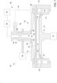
- FIG 1 is a schematic view of a substrate processing chamber (process chamber 100) including a gas delivery system 130 adapted for ALD processes.
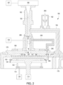
- Figure 2 is a cross-sectional view of the process chamber 100.
- Process chamber 100 includes a chamber body 102 having a processing volume within the chamber body 102 and beneath the chamber lid assembly 132.
- Slit valve 108 in the process chamber 100 provides access for a robot (not shown) to deliver and retrieve a substrate 110, such as a 200 mm or 300 mm semiconductor wafer or a glass substrate, to and from the process chamber 100.
- a chamber liner 177 is disposed along the walls of the process chamber 100 to protect the chamber from corrosive gases used during processing/cleaning.
- a substrate support 112 supports the substrate 110 on a substrate receiving surface 111 in the process chamber 100.
- the substrate support 112 is mounted to a lift motor 114 for raising and lowering the substrate support 112 and the substrate 110 disposed on the substrate support.
- a lift plate 116 (shown in Figure 2 ), connected to a lift motor 118, is mounted in the process chamber 100 to raise and lower lift pins 120 movably disposed through the substrate support 112.
- the lift pins 120 raise and lower the substrate 110 over the surface of the substrate support 112.
- the substrate support 112 may include a vacuum chuck (not shown), an electrostatic chuck (not shown), or a clamp ring (not shown) for securing the substrate 110 to the substrate support 112 during a deposition process.
- the temperature of the substrate support 112 may be adjusted to control the temperature of the substrate 110.
- substrate support 112 may be heated using an embedded heating element, such as a resistive heater (not shown), or may be heated using radiant heat, such as heating lamps (not shown) disposed above the substrate support 112.
- a purge ring 122 may be disposed on the substrate support 112 to define a purge channel 124 which provides a purge gas to a peripheral portion of the substrate 110 to prevent deposition on the peripheral portion of the substrate 110.
- Gas delivery system 130 is disposed at an upper portion of the chamber body 102 to provide a gas, such as a process gas and/or a purge gas, to process chamber 100.
- a vacuum system (not shown) is in communication with a pumping channel 179 to evacuate any desired gases from the process chamber 100 and to help maintain a desired pressure or pressure range inside the process chamber 100.
- the chamber lid assembly 132 includes a gas dispersion channel 134 extending through a central portion of the chamber lid assembly 132. As shown in Figures 1 and 2 , the gas dispersion channel 134 extends perpendicularly toward the substrate receiving surface 111 and also extends along a central axis 133 of the gas dispersion channel 134, through lid plate 170, and to lower surface 160. In some embodiments, an upper portion of the gas dispersion channel 134 is substantially cylindrical along central axis 133 and a lower portion of the gas dispersion channel 134 tapers away from central axis 133. The lower surface 160 is sized and shaped to substantially cover the substrate 110 disposed on the substrate receiving surface 111 of the substrate support 112.
- the lower surface 160 tapers from an outer edge of the lid plate 170 towards the gas dispersion channel 134.
- the gas delivery system 130 may provide two or more gasses to the gas dispersion channel 134 to process the substrate 110.
- the gas delivery system 130 may be coupled to the gas dispersion channel 134 via one gas inlet.
- the gas delivery system may be coupled to the gas dispersion channel 134 via a plurality of inlets.
- circular gas flow 174 which illustrates the flow of process gases through the gas dispersion channel 134, may contain various types of flow patterns.
- processing gases may be forced to make revolutions around central axis 133 of gas dispersion channel 134 while passing through the dispersion channel.
- the circular gas flow 174 may contain various types of circular flow patterns, such as a vortex pattern, a helix pattern, a spiral pattern, or derivatives thereof.
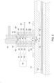
- the process chamber 100 further includes a gas distribution plate 125 having a plurality of apertures 126 disposed through the gas distribution plate 125.
- the gas distribution plate 125 extends to the surface of the gas dispersion channel 134 such that the only pathway from the gas dispersion channel 134 to the substrate is through the plurality of apertures 126 of the gas distribution plate 125.
- the gas distribution plate 125 advantageously creates a choked flow of gas through the gas distribution plate 125 resulting in a more uniform deposition on the substrate 110 and, thus, substantially eliminating the donut-shaped deposition caused by the rotational flow of gas.
- the gas distribution plate 125 is formed of a non-corrosive ceramic material such as, for example, aluminum oxide or aluminum nitride.
- each of the plurality of apertures 126 may have an equivalent fluid conductance.
- a density of the plurality of apertures 126 e.g., the number of apertures or the size of the openings of the apertures per unit area
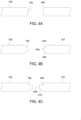
- the plurality of apertures 126 are depicted as cylindrical through holes, the plurality of apertures 126 may have different profiles.
- the aperture 126 is a cylindrical through hole having curved edges 402 that surround the aperture.
- the aperture 126 is a through hole having an upper portion 404 that tapers inwardly toward a center of the aperture, a cylindrical center portion 405 extending perpendicularly to an upper surface 127 of the gas distribution plate 125, and a lower portion 406 that tapers outwardly from the center of the aperture.
- the aperture 126 is a through hole having an upper portion 408 having a countersunk hole, a cylindrical center portion 409 extending perpendicularly to the upper surface 127 of the gas distribution plate 125, and a lower portion 410 that tapers outwardly from the center of the aperture.
- Other profiles of the plurality of apertures 126 may alternatively be used to achieve optimal deposition uniformity during processing of the substrate 110.
- the inventors believe that the diameter of gas dispersion channel 134, which is constant from the upper portion of gas dispersion channel 134 to a first point along central axis 133 and increasing from the first point to lower portion 135 of gas dispersion channel 134, allows less of an adiabatic expansion of a gas through gas dispersion channel 134 which helps to control the temperature of the process gas contained in the circular gas flow 174. For example, a sudden adiabatic expansion of a gas delivered into gas dispersion channel 134 may result in a drop in the temperature of the gas which may cause condensation of the gas and formation of droplets.
- Gas dispersion channel 134 that gradually tapers is believed to provide less of an adiabatic expansion of a gas. Therefore, more heat may be transferred to or from the gas, and, thus, the temperature of the gas may be more easily controlled by controlling the temperature of chamber lid assembly 132.
- Gas dispersion channel 134 may gradually taper and contain one or more tapered inner surfaces, such as a tapered straight surface, a concave surface, a convex surface, or combinations thereof or may contain sections of one or more tapered inner surfaces ( i.e., a portion tapered and a portion non-tapered).
- the upper portion of the gas dispersion channel 134 is defined by an insert 300 disposed in an inner region of a housing 375.
- the insert 300 includes a cap 302 at an upper portion of the insert 300 and a central passageway that at least partially defines the gas dispersion channel 134.
- the cap 302 extends over the housing 375 to hold the insert 300 in place.
- the insert 300 and cap 302 include a plurality of o-rings 385 disposed between the insert 300 and the housing 375 to ensure proper sealing.
- the insert 300 includes a plurality of circumferential apertures which, when the insert 300 is inserted into the housing 375, form a corresponding plurality of circumferential channels 360, 365, 370.
- the plurality of circumferential channels 360, 365, 370 are fluidly coupled to the gas dispersion channel 134 via a corresponding plurality of holes 340, 345, 350.
- the gas delivery system 130 is coupled to the gas dispersion channel 134 via a plurality of gas feed lines 310, 315, 320.
- the gas feed lines 310, 315, 320 are fluidly coupled to the plurality of circumferential channels 360, 365, 370 to provide one or more gases to the gas dispersion channel 134.
- the process chamber 100 further includes a chamber cleaning system including a remote plasma source (RPS) 190, an isolation collar 192 coupled to the RPS 190 at one end and the cap 302 at an opposite end, a heater plate 198 coupled to an upper surface of the lid plate 170, and a cleaning gas (i.e., purge gas) source 197 fluidly coupled to the RPS 190.
- the cleaning gas source may include any gas suitable for forming a plasma to clean the process chamber 100.
- the cleaning gas may be nitrogen trifluoride (NF 3 ).
- the isolation collar 192 includes an inner channel 193 that is fluidly coupled to the gas dispersion channel 134 through a plurality of holes 285 disposed in a central portion of the cap 302 to flow a plasma from the RPS 190 through the gas dispersion channel 134 and into the reaction zone 164.
- the heater plate 198 may be formed of stainless steel and include a plurality of resistive heating elements dispersed throughout the plate.
- a cleaning gas is flowed through the gas dispersion channel 134 and the reaction zone 164 after a first gas is provided to the gas dispersion channel 134 by the gas delivery system 130 to quickly purge the first gas from the gas dispersion channel 134 and the reaction zone 164.
- a second gas is provided by the gas delivery system 130 to the gas dispersion channel 134 and the cleaning gas is again flowed through the gas dispersion channel 134 to the reaction zone 164 to quickly purge the second gas from the gas dispersion channel 134 and the reaction zone 164.
- the addition of the gas distribution plate 125 chokes the flow of the cleaning gas to the pumping channel 179 and prolongs the cleaning process.
- an exhaust system 180 having an exhaust conduit 184 coupled to the isolation collar 192 at a first end 186 and to the pumping channel 179 at a second end 188.
- a valve 182 is disposed in the exhaust conduit 184 to selectively fluidly couple the exhaust conduit 184 to the inner channel 193.
- the valve 182 may be a plunger type valve having a plunger 202 that is moveable between a first position (shown in Figure 2 ) to fluidly couple the exhaust conduit 184 to the inner channel 193 and a second position to seal off the exhaust conduit 184 from the inner channel 193.
- the isolation collar 192 may be formed of any material that is non-reactive with the cleaning gas being used. In some embodiments, the isolation collar 192 may be formed of aluminum when the cleaning gas is NF 3 . In some embodiments, the isolation collar 192 and the insert 300 may be formed of aluminum and coated with a coating to prevent corrosion of the isolation collar 192 and the insert 300 from corrosive gases when used. For example, the coating may be formed of nickel or aluminum oxide.
- the RPS 190 operates at a temperature less than or equal to about 40 °C.
- a thermal isolation ring 394 is disposed between the isolation collar 192 and the cap 302.
- the thermal isolation ring 394 is formed of a metal with low thermal conductivity (e.g., lower than the thermal conductivity of the isolation collar 192 and the cap 302).
- an o-ring 385 may also be disposed between the isolation collar 192 and the cap 302 to further reduce the contact area between the isolation collar 192 and the cap 302.
- the combination of the thermal isolation ring 394 and the o-ring 385 acts as a thermal choke to ensure that the heat generated in the process chamber 100 does not adversely affect the RPS 190.
- the process chamber 100 may include a differential pumping line 250 to ensure that any process gases or byproducts trapped between o-rings 385 are exhausted to the pumping channel 179.
- the differential pumping line 250 is coupled to the lid plate 170 at a first end and to the housing 375 at a second end opposite the first end.
- the differential pumping line is fluidly coupled to the gas dispersion channel 134 and to one or more channels 260 formed at areas between two or more o-rings 385.
- the valve 182 is opened to exhaust the gas dispersion channel 134, the differential pumping line exhausts gases trapped between o-rings 385.
- a portion of lower surface 160 of chamber lid assembly 132 is contoured or angled downwardly and outwardly from a central opening coupled to the gas dispersion channel 134 to a peripheral portion of chamber lid assembly 132 to help provide an improved velocity profile of a gas flow from gas dispersion channel 134 across the surface of substrate 110 ( i.e., from the center of the substrate to the edge of the substrate).
- Lower surface 160 may contain one or more surfaces, such as a straight surface, a concave surface, a convex surface, or combinations thereof. In one embodiment, lower surface 160 is convexly funnel-shaped.
- a lower surface 160 is downwardly and outwardly sloping toward an edge of the substrate receiving surface 111 to help reduce the variation in the velocity of the process gases traveling between lower surface 160 of chamber lid assembly 132 and substrate 110 while assisting to provide uniform exposure of the surface of substrate 110 to a reactant gas.
- the components and parts of chamber lid assembly 132 may contain materials such as stainless steel, aluminum, nickel-plated aluminum, nickel, alloys thereof, or other suitable materials.
- lid plate 170 may be independently fabricated, machined, forged, or otherwise made from a metal, such as aluminum, an aluminum alloy, steel, stainless steel, alloys thereof, or combinations thereof.
- inner surface 131 of gas dispersion channel 134 and lower surface 160 of chamber lid assembly 132 may contain a mirror polished surface to help a flow of a gas along gas dispersion channel 134 and lower surface 160 of chamber lid assembly 132.
- substrate 110 is delivered to process chamber 100 through slit valve 108 by a robot (not shown).
- Substrate 110 is positioned on substrate support 112 through cooperation of lift pins 120 and the robot.
- Substrate support 112 raises substrate 110 into close opposition to a lower surface of the gas distribution plate 125.
- a first gas flow may be injected into gas dispersion channel 134 of process chamber 100 by the gas delivery system 130 together or separately ( i.e., pulses) with a second gas flow.
- the first gas flow may contain a continuous flow of a purge gas from a purge gas source and pulses of a reactant gas from a reactant gas source or may contain pulses of a reactant gas from the reactant gas source and pulses of a purge gas from the purge gas source.
- the second gas flow may contain a continuous flow of a purge gas from a purge gas source and pulses of a reactant gas from a reactant gas source or may contain pulses of a reactant gas from a reactant gas source and pulses of a purge gas from a purge gas source.
- the circular gas flow 174 travels through gas dispersion channel 134 and subsequently through the plurality of apertures 126 in the gas distribution plate 125.
- the gas is then deposited on the surface of substrate 110.
- Lower surface 160 of chamber lid assembly 132 which is downwardly sloping, helps reduce the variation of the velocity of the gas flow across the surface of gas distribution plate 125.
- Excess gas, by-products, etc. flow into the pumping channel 179 and are then exhausted from process chamber 100.
- the heater plate 198 may heat the chamber lid assembly 132 to a predetermined temperature to heat any solid byproducts that have accumulated on walls of the process chamber 100 (or a processing kit disposed in the chamber). As a result, any accumulated solid byproducts are vaporized.
- the vaporized byproducts are evacuated by a vacuum system (not shown) and pumping channel 179.
- the predetermined temperature is greater than or equal to 150 °C.
- Figure 5 illustrates a method 500 of processing a substrate in accordance with some embodiments of the present disclosure.
- a first process gas is flowed from the gas delivery system 130 into the gas dispersion channel 134 and the reaction zone 164.
- the first process gas is flowed through the plurality of apertures 126 in the gas distribution plate 125 and onto the substrate 110.
- a cleaning gas is flowed into the gas dispersion channel 134 and the reaction zone 164 to purge the first process gas.
- the cleaning gas is exhausted via the exhaust system 180.
- a second process gas is flowed into the gas dispersion channel 134 and the reaction zone 164.
- the second process gas is flowed through the plurality of apertures 126 in the gas distribution plate 125 and onto the substrate 110.
- the cleaning gas is flowed into the gas dispersion channel 134 and the reaction zone 164 to purge the second process gas.
- the cleaning gas is exhausted via the exhaust system 180.
Landscapes
- Chemical & Material Sciences (AREA)
- Engineering & Computer Science (AREA)
- Metallurgy (AREA)
- Chemical Kinetics & Catalysis (AREA)
- Materials Engineering (AREA)
- Mechanical Engineering (AREA)
- General Chemical & Material Sciences (AREA)
- Organic Chemistry (AREA)
- Physics & Mathematics (AREA)
- Plasma & Fusion (AREA)
- Analytical Chemistry (AREA)
- Electromagnetism (AREA)
- Chemical Vapour Deposition (AREA)
- Crystals, And After-Treatments Of Crystals (AREA)
Claims (12)
- Chambre de traitement de substrat, comprenant :un corps de chambre (102) ;un ensemble couvercle de chambre (132) comportant un boîtier (375) enfermant un canal de dispersion de gaz en forme d'entonnoir (134) qui s'étend le long d'un axe central (133) et qui comporte une partie supérieure et une partie inférieure ;un système distributeur de gaz (130) configuré pour fournir au moins deux gaz au canal de dispersion de gaz (134) ;une plaque de couvercle (170) accouplée au boîtier (375) et comportant une surface inférieure profilée (160) qui est en pente vers le bas de façon à s'étendre vers le bas et vers l'extérieur d'une ouverture centrale accouplée à la partie inférieure du canal de dispersion de gaz en forme d'entonnoir (134) à une partie périphérique de la plaque de couvercle (170) ; etune plaque de distribution de gaz (125) disposée au-dessous de la plaque de couvercle (170) et comportant une pluralité d'ouvertures (126) ménagées à travers la plaque de distribution de gaz (125), dans laquellela surface inférieure profilée (160) de la plaque de couvercle (170) s'étend vers la plaque de distribution de gaz (125) et la contacte, de sorte que la plaque de distribution de gaz (125) s'étende vers une surface du canal de dispersion de gaz (134) pour que l'unique passage du canal de dispersion de gaz (134) au substrat passe par la pluralité d'ouvertures de la plaque de distribution de gaz (125) ; etune source de plasma à distance, dite RPS, (190) accouplée en communication fluidique au canal de dispersion de gaz (134) ;une source de gaz de nettoyage (197) accouplée en communication fluidique à la RPS (190) ; etune bague d'isolement (192) accouplée entre la source de plasma à distance (190) et le boîtier (375), la bague d'isolement (192) comportant un canal interne s'étendant à travers la bague d'isolement (192) pour un accouplement en communication fluidique de la source de plasma à distance (190) et du canal de dispersion de gaz (134), dans laquelle un système d'échappement (180) comportant un conduit d'échappement (184) est accouplé à la bague d'isolement (192).
- Chambre de traitement de substrat selon la revendication 1, dans laquelle le conduit d'échappement (184) est accouplé à la bague d'isolement (192) au niveau d'une première extrémité et est accouplé à un canal de pompage principal (179) au niveau d'une seconde extrémité ; et
une vanne est accouplée au conduit d'échappement (184) pour ouvrir ou fermer sélectivement le conduit d'échappement. - Chambre de traitement de substrat selon la revendication 1, dans laquelle le boîtier (375) comprend une région interne ; et comprenant en outre :
un insert (300) disposé dans la région interne et comportant un passage central qui délimite au moins partiellement le canal de dispersion de gaz (134). - Chambre de traitement de substrat selon la revendication 3, comprenant en outre :une conduite de pompage différentiel (250) accouplée à l'insert (300) au niveau d'une première extrémité et à la plaque de couvercle (170) au niveau d'une seconde extrémité,dans laquelle la plaque de couvercle (170) comprend un ou plusieurs canaux disposés dans une zone de la plaque de couvercle (170) entre au moins deux joints toriques (385) pour évacuer des gaz piégés entre les joints toriques (385).
- Chambre de traitement de substrat selon l'une quelconque des revendications 1 à 4, comprenant en outre :
une plaque chauffante (198) accouplée à une surface supérieure de la plaque de couvercle (170) pour chauffer la plaque de couvercle (170) à une température prédéterminée. - Chambre de traitement de substrat selon l'une quelconque des revendications 1 à 4, dans laquelle une densité des ouvertures de la pluralité d'ouvertures (126) varie d'un bout à l'autre de la plaque de distribution de gaz (125).
- Chambre de traitement de substrat selon l'une quelconque des revendications 1 à 4, dans laquelle les ouvertures de la pluralité d'ouvertures (126) ont une conductance fluide équivalente.
- Chambre de traitement de substrat selon l'une quelconque des revendications 1 à 4, dans laquelle la plaque de distribution de gaz (125) est formée d'un matériau céramique non corrosif.
- Chambre de traitement de substrat selon l'une quelconque des revendications 1 à 4, comprenant en outre :
une plaque chauffante (198) accouplée à une surface supérieure de la plaque de couvercle (170) pour chauffer la plaque de couvercle (170) à une température prédéterminée, dans laquelle la plaque de distribution de gaz (125) est formée d'un matériau céramique non corrosif. - Procédé de traitement d'un substrat dans une chambre de traitement de substrat selon l'une quelconque des revendications 1 à 9, le procédé comprenant les étapes consistant à :amener un premier gaz de procédé à s'écouler (505) dans le canal de dispersion de gaz (134) de l'ensemble couvercle de chambre (132) et dans une zone de réaction de la chambre de traitement de substrat ;amener le premier gaz de procédé à s'écouler (510) à travers les ouvertures de la pluralité d'ouvertures (126) de la plaque de distribution de gaz (125) disposée dans la zone de réaction et sur le substrat ;amener le gaz de nettoyage à s'écouler (515) dans le canal de dispersion de gaz (134) et dans la zone de réaction ;évacuer (520) le gaz de nettoyage par le biais du système d'échappement (180) ;amener un second gaz de procédé à s'écouler (525) dans le canal de dispersion de gaz (134) et dans la zone de réaction ;amener le second gaz de procédé à s'écouler (530) à travers les ouvertures de la pluralité d'ouvertures (126) de la plaque de distribution de gaz (125) et sur le substrat ;amener le gaz de nettoyage à s'écouler (535) dans le canal de dispersion de gaz (134) et dans la zone de réaction ; etévacuer (540) le gaz de nettoyage par le biais du système d'échappement (180).
- Procédé selon la revendication 10, comprenant en outre l'étape consistant à :
chauffer l'ensemble couvercle (132) à une température prédéterminée. - Procédé selon la revendication 11, dans lequel la température prédéterminée est supérieure ou égale à 150 °C.
Applications Claiming Priority (3)
| Application Number | Priority Date | Filing Date | Title |
|---|---|---|---|
| US201562151180P | 2015-04-22 | 2015-04-22 | |
| US14/734,838 US11384432B2 (en) | 2015-04-22 | 2015-06-09 | Atomic layer deposition chamber with funnel-shaped gas dispersion channel and gas distribution plate |
| PCT/US2016/028253 WO2016172085A1 (fr) | 2015-04-22 | 2016-04-19 | Chambre de dépôt de couche atomique avec canal de dispersion en forme d'entonnoir et plaque de distribution de gaz |
Publications (3)
| Publication Number | Publication Date |
|---|---|
| EP3286352A1 EP3286352A1 (fr) | 2018-02-28 |
| EP3286352A4 EP3286352A4 (fr) | 2019-01-23 |
| EP3286352B1 true EP3286352B1 (fr) | 2025-06-18 |
Family
ID=57144181
Family Applications (1)
| Application Number | Title | Priority Date | Filing Date |
|---|---|---|---|
| EP16783678.2A Active EP3286352B1 (fr) | 2015-04-22 | 2016-04-19 | Chambre de dépôt de couche atomique avec canal de dispersion en forme d'entonnoir et plaque de distribution de gaz |
Country Status (8)
| Country | Link |
|---|---|
| US (2) | US11384432B2 (fr) |
| EP (1) | EP3286352B1 (fr) |
| KR (2) | KR102640272B1 (fr) |
| CN (2) | CN107532297B (fr) |
| IL (2) | IL284142B2 (fr) |
| SG (2) | SG10202111772XA (fr) |
| TW (2) | TWI722871B (fr) |
| WO (1) | WO2016172085A1 (fr) |
Families Citing this family (403)
| Publication number | Priority date | Publication date | Assignee | Title |
|---|---|---|---|---|
| US10378106B2 (en) | 2008-11-14 | 2019-08-13 | Asm Ip Holding B.V. | Method of forming insulation film by modified PEALD |
| US9394608B2 (en) | 2009-04-06 | 2016-07-19 | Asm America, Inc. | Semiconductor processing reactor and components thereof |
| US8802201B2 (en) | 2009-08-14 | 2014-08-12 | Asm America, Inc. | Systems and methods for thin-film deposition of metal oxides using excited nitrogen-oxygen species |
| US9312155B2 (en) | 2011-06-06 | 2016-04-12 | Asm Japan K.K. | High-throughput semiconductor-processing apparatus equipped with multiple dual-chamber modules |
| US10364496B2 (en) | 2011-06-27 | 2019-07-30 | Asm Ip Holding B.V. | Dual section module having shared and unshared mass flow controllers |
| US10854498B2 (en) | 2011-07-15 | 2020-12-01 | Asm Ip Holding B.V. | Wafer-supporting device and method for producing same |
| US20130023129A1 (en) | 2011-07-20 | 2013-01-24 | Asm America, Inc. | Pressure transmitter for a semiconductor processing environment |
| US9017481B1 (en) | 2011-10-28 | 2015-04-28 | Asm America, Inc. | Process feed management for semiconductor substrate processing |
| US9659799B2 (en) | 2012-08-28 | 2017-05-23 | Asm Ip Holding B.V. | Systems and methods for dynamic semiconductor process scheduling |
| US10714315B2 (en) | 2012-10-12 | 2020-07-14 | Asm Ip Holdings B.V. | Semiconductor reaction chamber showerhead |
| US20160376700A1 (en) | 2013-02-01 | 2016-12-29 | Asm Ip Holding B.V. | System for treatment of deposition reactor |
| US9589770B2 (en) | 2013-03-08 | 2017-03-07 | Asm Ip Holding B.V. | Method and systems for in-situ formation of intermediate reactive species |
| US9484191B2 (en) | 2013-03-08 | 2016-11-01 | Asm Ip Holding B.V. | Pulsed remote plasma method and system |
| US9240412B2 (en) | 2013-09-27 | 2016-01-19 | Asm Ip Holding B.V. | Semiconductor structure and device and methods of forming same using selective epitaxial process |
| US10683571B2 (en) | 2014-02-25 | 2020-06-16 | Asm Ip Holding B.V. | Gas supply manifold and method of supplying gases to chamber using same |
| US10167557B2 (en) | 2014-03-18 | 2019-01-01 | Asm Ip Holding B.V. | Gas distribution system, reactor including the system, and methods of using the same |
| US11015245B2 (en) | 2014-03-19 | 2021-05-25 | Asm Ip Holding B.V. | Gas-phase reactor and system having exhaust plenum and components thereof |
| US10858737B2 (en) | 2014-07-28 | 2020-12-08 | Asm Ip Holding B.V. | Showerhead assembly and components thereof |
| US9890456B2 (en) | 2014-08-21 | 2018-02-13 | Asm Ip Holding B.V. | Method and system for in situ formation of gas-phase compounds |
| US9793096B2 (en) * | 2014-09-12 | 2017-10-17 | Lam Research Corporation | Systems and methods for suppressing parasitic plasma and reducing within-wafer non-uniformity |
| US10407771B2 (en) * | 2014-10-06 | 2019-09-10 | Applied Materials, Inc. | Atomic layer deposition chamber with thermal lid |
| US9657845B2 (en) | 2014-10-07 | 2017-05-23 | Asm Ip Holding B.V. | Variable conductance gas distribution apparatus and method |
| US10941490B2 (en) | 2014-10-07 | 2021-03-09 | Asm Ip Holding B.V. | Multiple temperature range susceptor, assembly, reactor and system including the susceptor, and methods of using the same |
| KR102263121B1 (ko) | 2014-12-22 | 2021-06-09 | 에이에스엠 아이피 홀딩 비.브이. | 반도체 소자 및 그 제조 방법 |
| US10529542B2 (en) | 2015-03-11 | 2020-01-07 | Asm Ip Holdings B.V. | Cross-flow reactor and method |
| US10276355B2 (en) | 2015-03-12 | 2019-04-30 | Asm Ip Holding B.V. | Multi-zone reactor, system including the reactor, and method of using the same |
| US11384432B2 (en) | 2015-04-22 | 2022-07-12 | Applied Materials, Inc. | Atomic layer deposition chamber with funnel-shaped gas dispersion channel and gas distribution plate |
| KR101792941B1 (ko) * | 2015-04-30 | 2017-11-02 | 어드밴스드 마이크로 패브리케이션 이큅먼트 인코퍼레이티드, 상하이 | 화학기상증착장치 및 그 세정방법 |
| US10458018B2 (en) | 2015-06-26 | 2019-10-29 | Asm Ip Holding B.V. | Structures including metal carbide material, devices including the structures, and methods of forming same |
| US10600673B2 (en) | 2015-07-07 | 2020-03-24 | Asm Ip Holding B.V. | Magnetic susceptor to baseplate seal |
| US9960072B2 (en) | 2015-09-29 | 2018-05-01 | Asm Ip Holding B.V. | Variable adjustment for precise matching of multiple chamber cavity housings |
| US10211308B2 (en) | 2015-10-21 | 2019-02-19 | Asm Ip Holding B.V. | NbMC layers |
| US10322384B2 (en) | 2015-11-09 | 2019-06-18 | Asm Ip Holding B.V. | Counter flow mixer for process chamber |
| US11139308B2 (en) | 2015-12-29 | 2021-10-05 | Asm Ip Holding B.V. | Atomic layer deposition of III-V compounds to form V-NAND devices |
| US10529554B2 (en) | 2016-02-19 | 2020-01-07 | Asm Ip Holding B.V. | Method for forming silicon nitride film selectively on sidewalls or flat surfaces of trenches |
| US10468251B2 (en) | 2016-02-19 | 2019-11-05 | Asm Ip Holding B.V. | Method for forming spacers using silicon nitride film for spacer-defined multiple patterning |
| US10501866B2 (en) | 2016-03-09 | 2019-12-10 | Asm Ip Holding B.V. | Gas distribution apparatus for improved film uniformity in an epitaxial system |
| US10343920B2 (en) | 2016-03-18 | 2019-07-09 | Asm Ip Holding B.V. | Aligned carbon nanotubes |
| US9892913B2 (en) | 2016-03-24 | 2018-02-13 | Asm Ip Holding B.V. | Radial and thickness control via biased multi-port injection settings |
| US10865475B2 (en) | 2016-04-21 | 2020-12-15 | Asm Ip Holding B.V. | Deposition of metal borides and silicides |
| US10190213B2 (en) | 2016-04-21 | 2019-01-29 | Asm Ip Holding B.V. | Deposition of metal borides |
| US10032628B2 (en) | 2016-05-02 | 2018-07-24 | Asm Ip Holding B.V. | Source/drain performance through conformal solid state doping |
| US10367080B2 (en) | 2016-05-02 | 2019-07-30 | Asm Ip Holding B.V. | Method of forming a germanium oxynitride film |
| KR102592471B1 (ko) | 2016-05-17 | 2023-10-20 | 에이에스엠 아이피 홀딩 비.브이. | 금속 배선 형성 방법 및 이를 이용한 반도체 장치의 제조 방법 |
| US11453943B2 (en) | 2016-05-25 | 2022-09-27 | Asm Ip Holding B.V. | Method for forming carbon-containing silicon/metal oxide or nitride film by ALD using silicon precursor and hydrocarbon precursor |
| KR102102320B1 (ko) * | 2016-06-28 | 2020-04-22 | 주식회사 원익아이피에스 | 기판 처리 장치 및 그것을 이용한 박막 증착 방법 |
| US10388509B2 (en) | 2016-06-28 | 2019-08-20 | Asm Ip Holding B.V. | Formation of epitaxial layers via dislocation filtering |
| US9859151B1 (en) | 2016-07-08 | 2018-01-02 | Asm Ip Holding B.V. | Selective film deposition method to form air gaps |
| US10612137B2 (en) | 2016-07-08 | 2020-04-07 | Asm Ip Holdings B.V. | Organic reactants for atomic layer deposition |
| US10714385B2 (en) | 2016-07-19 | 2020-07-14 | Asm Ip Holding B.V. | Selective deposition of tungsten |
| KR102354490B1 (ko) | 2016-07-27 | 2022-01-21 | 에이에스엠 아이피 홀딩 비.브이. | 기판 처리 방법 |
| US9887082B1 (en) | 2016-07-28 | 2018-02-06 | Asm Ip Holding B.V. | Method and apparatus for filling a gap |
| US10395919B2 (en) | 2016-07-28 | 2019-08-27 | Asm Ip Holding B.V. | Method and apparatus for filling a gap |
| KR102532607B1 (ko) | 2016-07-28 | 2023-05-15 | 에이에스엠 아이피 홀딩 비.브이. | 기판 가공 장치 및 그 동작 방법 |
| US9812320B1 (en) | 2016-07-28 | 2017-11-07 | Asm Ip Holding B.V. | Method and apparatus for filling a gap |
| KR102613349B1 (ko) | 2016-08-25 | 2023-12-14 | 에이에스엠 아이피 홀딩 비.브이. | 배기 장치 및 이를 이용한 기판 가공 장치와 박막 제조 방법 |
| US10410943B2 (en) | 2016-10-13 | 2019-09-10 | Asm Ip Holding B.V. | Method for passivating a surface of a semiconductor and related systems |
| US10643826B2 (en) | 2016-10-26 | 2020-05-05 | Asm Ip Holdings B.V. | Methods for thermally calibrating reaction chambers |
| US11532757B2 (en) | 2016-10-27 | 2022-12-20 | Asm Ip Holding B.V. | Deposition of charge trapping layers |
| US10435790B2 (en) | 2016-11-01 | 2019-10-08 | Asm Ip Holding B.V. | Method of subatmospheric plasma-enhanced ALD using capacitively coupled electrodes with narrow gap |
| US10229833B2 (en) | 2016-11-01 | 2019-03-12 | Asm Ip Holding B.V. | Methods for forming a transition metal nitride film on a substrate by atomic layer deposition and related semiconductor device structures |
| US10643904B2 (en) | 2016-11-01 | 2020-05-05 | Asm Ip Holdings B.V. | Methods for forming a semiconductor device and related semiconductor device structures |
| US10714350B2 (en) | 2016-11-01 | 2020-07-14 | ASM IP Holdings, B.V. | Methods for forming a transition metal niobium nitride film on a substrate by atomic layer deposition and related semiconductor device structures |
| US10134757B2 (en) | 2016-11-07 | 2018-11-20 | Asm Ip Holding B.V. | Method of processing a substrate and a device manufactured by using the method |
| KR102546317B1 (ko) | 2016-11-15 | 2023-06-21 | 에이에스엠 아이피 홀딩 비.브이. | 기체 공급 유닛 및 이를 포함하는 기판 처리 장치 |
| US10340135B2 (en) | 2016-11-28 | 2019-07-02 | Asm Ip Holding B.V. | Method of topologically restricted plasma-enhanced cyclic deposition of silicon or metal nitride |
| KR102762543B1 (ko) | 2016-12-14 | 2025-02-05 | 에이에스엠 아이피 홀딩 비.브이. | 기판 처리 장치 |
| US11581186B2 (en) | 2016-12-15 | 2023-02-14 | Asm Ip Holding B.V. | Sequential infiltration synthesis apparatus |
| US11447861B2 (en) | 2016-12-15 | 2022-09-20 | Asm Ip Holding B.V. | Sequential infiltration synthesis apparatus and a method of forming a patterned structure |
| KR102700194B1 (ko) | 2016-12-19 | 2024-08-28 | 에이에스엠 아이피 홀딩 비.브이. | 기판 처리 장치 |
| US10269558B2 (en) | 2016-12-22 | 2019-04-23 | Asm Ip Holding B.V. | Method of forming a structure on a substrate |
| US10867788B2 (en) | 2016-12-28 | 2020-12-15 | Asm Ip Holding B.V. | Method of forming a structure on a substrate |
| US11390950B2 (en) | 2017-01-10 | 2022-07-19 | Asm Ip Holding B.V. | Reactor system and method to reduce residue buildup during a film deposition process |
| EP3568504A4 (fr) * | 2017-01-16 | 2021-01-06 | Sustainable Energy Solutions, LLC | Procédé et appareil permettant de prévenir la désublimation dans un échangeur de chaleur à contact direct |
| US10655221B2 (en) | 2017-02-09 | 2020-05-19 | Asm Ip Holding B.V. | Method for depositing oxide film by thermal ALD and PEALD |
| US10468261B2 (en) | 2017-02-15 | 2019-11-05 | Asm Ip Holding B.V. | Methods for forming a metallic film on a substrate by cyclical deposition and related semiconductor device structures |
| US9972501B1 (en) * | 2017-03-14 | 2018-05-15 | Nano-Master, Inc. | Techniques and systems for continuous-flow plasma enhanced atomic layer deposition (PEALD) |
| US10283353B2 (en) | 2017-03-29 | 2019-05-07 | Asm Ip Holding B.V. | Method of reforming insulating film deposited on substrate with recess pattern |
| US10529563B2 (en) | 2017-03-29 | 2020-01-07 | Asm Ip Holdings B.V. | Method for forming doped metal oxide films on a substrate by cyclical deposition and related semiconductor device structures |
| KR102457289B1 (ko) | 2017-04-25 | 2022-10-21 | 에이에스엠 아이피 홀딩 비.브이. | 박막 증착 방법 및 반도체 장치의 제조 방법 |
| US10446393B2 (en) | 2017-05-08 | 2019-10-15 | Asm Ip Holding B.V. | Methods for forming silicon-containing epitaxial layers and related semiconductor device structures |
| US10892156B2 (en) | 2017-05-08 | 2021-01-12 | Asm Ip Holding B.V. | Methods for forming a silicon nitride film on a substrate and related semiconductor device structures |
| US10770286B2 (en) | 2017-05-08 | 2020-09-08 | Asm Ip Holdings B.V. | Methods for selectively forming a silicon nitride film on a substrate and related semiconductor device structures |
| US10504742B2 (en) | 2017-05-31 | 2019-12-10 | Asm Ip Holding B.V. | Method of atomic layer etching using hydrogen plasma |
| US10886123B2 (en) | 2017-06-02 | 2021-01-05 | Asm Ip Holding B.V. | Methods for forming low temperature semiconductor layers and related semiconductor device structures |
| US12040200B2 (en) | 2017-06-20 | 2024-07-16 | Asm Ip Holding B.V. | Semiconductor processing apparatus and methods for calibrating a semiconductor processing apparatus |
| US11306395B2 (en) | 2017-06-28 | 2022-04-19 | Asm Ip Holding B.V. | Methods for depositing a transition metal nitride film on a substrate by atomic layer deposition and related deposition apparatus |
| US10685834B2 (en) | 2017-07-05 | 2020-06-16 | Asm Ip Holdings B.V. | Methods for forming a silicon germanium tin layer and related semiconductor device structures |
| TWI794238B (zh) | 2017-07-13 | 2023-03-01 | 荷蘭商Asm智慧財產控股公司 | 於單一加工腔室中自半導體膜移除氧化物及碳之裝置及方法 |
| KR20190009245A (ko) | 2017-07-18 | 2019-01-28 | 에이에스엠 아이피 홀딩 비.브이. | 반도체 소자 구조물 형성 방법 및 관련된 반도체 소자 구조물 |
| US11374112B2 (en) | 2017-07-19 | 2022-06-28 | Asm Ip Holding B.V. | Method for depositing a group IV semiconductor and related semiconductor device structures |
| US10541333B2 (en) | 2017-07-19 | 2020-01-21 | Asm Ip Holding B.V. | Method for depositing a group IV semiconductor and related semiconductor device structures |
| US11018002B2 (en) | 2017-07-19 | 2021-05-25 | Asm Ip Holding B.V. | Method for selectively depositing a Group IV semiconductor and related semiconductor device structures |
| US10605530B2 (en) | 2017-07-26 | 2020-03-31 | Asm Ip Holding B.V. | Assembly of a liner and a flange for a vertical furnace as well as the liner and the vertical furnace |
| US10590535B2 (en) | 2017-07-26 | 2020-03-17 | Asm Ip Holdings B.V. | Chemical treatment, deposition and/or infiltration apparatus and method for using the same |
| US10312055B2 (en) | 2017-07-26 | 2019-06-04 | Asm Ip Holding B.V. | Method of depositing film by PEALD using negative bias |
| TWI815813B (zh) | 2017-08-04 | 2023-09-21 | 荷蘭商Asm智慧財產控股公司 | 用於分配反應腔內氣體的噴頭總成 |
| US10770336B2 (en) | 2017-08-08 | 2020-09-08 | Asm Ip Holding B.V. | Substrate lift mechanism and reactor including same |
| US10692741B2 (en) | 2017-08-08 | 2020-06-23 | Asm Ip Holdings B.V. | Radiation shield |
| US11139191B2 (en) | 2017-08-09 | 2021-10-05 | Asm Ip Holding B.V. | Storage apparatus for storing cassettes for substrates and processing apparatus equipped therewith |
| US11769682B2 (en) | 2017-08-09 | 2023-09-26 | Asm Ip Holding B.V. | Storage apparatus for storing cassettes for substrates and processing apparatus equipped therewith |
| US10249524B2 (en) | 2017-08-09 | 2019-04-02 | Asm Ip Holding B.V. | Cassette holder assembly for a substrate cassette and holding member for use in such assembly |
| US20190048467A1 (en) * | 2017-08-10 | 2019-02-14 | Applied Materials, Inc. | Showerhead and process chamber incorporating same |
| USD900036S1 (en) | 2017-08-24 | 2020-10-27 | Asm Ip Holding B.V. | Heater electrical connector and adapter |
| US11830730B2 (en) | 2017-08-29 | 2023-11-28 | Asm Ip Holding B.V. | Layer forming method and apparatus |
| US11164737B2 (en) * | 2017-08-30 | 2021-11-02 | Applied Materials, Inc. | Integrated epitaxy and preclean system |
| US11056344B2 (en) | 2017-08-30 | 2021-07-06 | Asm Ip Holding B.V. | Layer forming method |
| US11295980B2 (en) | 2017-08-30 | 2022-04-05 | Asm Ip Holding B.V. | Methods for depositing a molybdenum metal film over a dielectric surface of a substrate by a cyclical deposition process and related semiconductor device structures |
| KR102491945B1 (ko) | 2017-08-30 | 2023-01-26 | 에이에스엠 아이피 홀딩 비.브이. | 기판 처리 장치 |
| KR102401446B1 (ko) | 2017-08-31 | 2022-05-24 | 에이에스엠 아이피 홀딩 비.브이. | 기판 처리 장치 |
| US10147597B1 (en) | 2017-09-14 | 2018-12-04 | Lam Research Corporation | Turbulent flow spiral multi-zone precursor vaporizer |
| US10607895B2 (en) | 2017-09-18 | 2020-03-31 | Asm Ip Holdings B.V. | Method for forming a semiconductor device structure comprising a gate fill metal |
| KR102630301B1 (ko) | 2017-09-21 | 2024-01-29 | 에이에스엠 아이피 홀딩 비.브이. | 침투성 재료의 순차 침투 합성 방법 처리 및 이를 이용하여 형성된 구조물 및 장치 |
| US10844484B2 (en) | 2017-09-22 | 2020-11-24 | Asm Ip Holding B.V. | Apparatus for dispensing a vapor phase reactant to a reaction chamber and related methods |
| US10658205B2 (en) | 2017-09-28 | 2020-05-19 | Asm Ip Holdings B.V. | Chemical dispensing apparatus and methods for dispensing a chemical to a reaction chamber |
| US10403504B2 (en) | 2017-10-05 | 2019-09-03 | Asm Ip Holding B.V. | Method for selectively depositing a metallic film on a substrate |
| US10319588B2 (en) | 2017-10-10 | 2019-06-11 | Asm Ip Holding B.V. | Method for depositing a metal chalcogenide on a substrate by cyclical deposition |
| US10923344B2 (en) | 2017-10-30 | 2021-02-16 | Asm Ip Holding B.V. | Methods for forming a semiconductor structure and related semiconductor structures |
| US10910262B2 (en) | 2017-11-16 | 2021-02-02 | Asm Ip Holding B.V. | Method of selectively depositing a capping layer structure on a semiconductor device structure |
| KR102443047B1 (ko) | 2017-11-16 | 2022-09-14 | 에이에스엠 아이피 홀딩 비.브이. | 기판 처리 장치 방법 및 그에 의해 제조된 장치 |
| US11022879B2 (en) | 2017-11-24 | 2021-06-01 | Asm Ip Holding B.V. | Method of forming an enhanced unexposed photoresist layer |
| TWI791689B (zh) | 2017-11-27 | 2023-02-11 | 荷蘭商Asm智慧財產控股私人有限公司 | 包括潔淨迷你環境之裝置 |
| WO2019103613A1 (fr) | 2017-11-27 | 2019-05-31 | Asm Ip Holding B.V. | Dispositif de stockage pour stocker des cassettes de tranches destiné à être utilisé avec un four discontinu |
| US10290508B1 (en) | 2017-12-05 | 2019-05-14 | Asm Ip Holding B.V. | Method for forming vertical spacers for spacer-defined patterning |
| US10872771B2 (en) | 2018-01-16 | 2020-12-22 | Asm Ip Holding B. V. | Method for depositing a material film on a substrate within a reaction chamber by a cyclical deposition process and related device structures |
| TWI799494B (zh) | 2018-01-19 | 2023-04-21 | 荷蘭商Asm 智慧財產控股公司 | 沈積方法 |
| US11482412B2 (en) | 2018-01-19 | 2022-10-25 | Asm Ip Holding B.V. | Method for depositing a gap-fill layer by plasma-assisted deposition |
| USD903477S1 (en) | 2018-01-24 | 2020-12-01 | Asm Ip Holdings B.V. | Metal clamp |
| US11018047B2 (en) | 2018-01-25 | 2021-05-25 | Asm Ip Holding B.V. | Hybrid lift pin |
| USD880437S1 (en) | 2018-02-01 | 2020-04-07 | Asm Ip Holding B.V. | Gas supply plate for semiconductor manufacturing apparatus |
| US10535516B2 (en) | 2018-02-01 | 2020-01-14 | Asm Ip Holdings B.V. | Method for depositing a semiconductor structure on a surface of a substrate and related semiconductor structures |
| US11081345B2 (en) | 2018-02-06 | 2021-08-03 | Asm Ip Holding B.V. | Method of post-deposition treatment for silicon oxide film |
| US10896820B2 (en) | 2018-02-14 | 2021-01-19 | Asm Ip Holding B.V. | Method for depositing a ruthenium-containing film on a substrate by a cyclical deposition process |
| WO2019158960A1 (fr) | 2018-02-14 | 2019-08-22 | Asm Ip Holding B.V. | Procédé de dépôt d'un film contenant du ruthénium sur un substrat par un processus de dépôt cyclique |
| US10731249B2 (en) | 2018-02-15 | 2020-08-04 | Asm Ip Holding B.V. | Method of forming a transition metal containing film on a substrate by a cyclical deposition process, a method for supplying a transition metal halide compound to a reaction chamber, and related vapor deposition apparatus |
| US10658181B2 (en) | 2018-02-20 | 2020-05-19 | Asm Ip Holding B.V. | Method of spacer-defined direct patterning in semiconductor fabrication |
| KR102636427B1 (ko) | 2018-02-20 | 2024-02-13 | 에이에스엠 아이피 홀딩 비.브이. | 기판 처리 방법 및 장치 |
| US10975470B2 (en) | 2018-02-23 | 2021-04-13 | Asm Ip Holding B.V. | Apparatus for detecting or monitoring for a chemical precursor in a high temperature environment |
| US11473195B2 (en) | 2018-03-01 | 2022-10-18 | Asm Ip Holding B.V. | Semiconductor processing apparatus and a method for processing a substrate |
| US11014853B2 (en) * | 2018-03-07 | 2021-05-25 | Applied Materials, Inc. | Y2O3—ZrO2 erosion resistant material for chamber components in plasma environments |
| US11629406B2 (en) | 2018-03-09 | 2023-04-18 | Asm Ip Holding B.V. | Semiconductor processing apparatus comprising one or more pyrometers for measuring a temperature of a substrate during transfer of the substrate |
| US11114283B2 (en) | 2018-03-16 | 2021-09-07 | Asm Ip Holding B.V. | Reactor, system including the reactor, and methods of manufacturing and using same |
| KR102646467B1 (ko) | 2018-03-27 | 2024-03-11 | 에이에스엠 아이피 홀딩 비.브이. | 기판 상에 전극을 형성하는 방법 및 전극을 포함하는 반도체 소자 구조 |
| US11088002B2 (en) | 2018-03-29 | 2021-08-10 | Asm Ip Holding B.V. | Substrate rack and a substrate processing system and method |
| US11230766B2 (en) | 2018-03-29 | 2022-01-25 | Asm Ip Holding B.V. | Substrate processing apparatus and method |
| US10510536B2 (en) | 2018-03-29 | 2019-12-17 | Asm Ip Holding B.V. | Method of depositing a co-doped polysilicon film on a surface of a substrate within a reaction chamber |
| KR102501472B1 (ko) | 2018-03-30 | 2023-02-20 | 에이에스엠 아이피 홀딩 비.브이. | 기판 처리 방법 |
| KR102600229B1 (ko) | 2018-04-09 | 2023-11-10 | 에이에스엠 아이피 홀딩 비.브이. | 기판 지지 장치, 이를 포함하는 기판 처리 장치 및 기판 처리 방법 |
| TWI843623B (zh) | 2018-05-08 | 2024-05-21 | 荷蘭商Asm Ip私人控股有限公司 | 藉由循環沉積製程於基板上沉積氧化物膜之方法及相關裝置結構 |
| US12025484B2 (en) | 2018-05-08 | 2024-07-02 | Asm Ip Holding B.V. | Thin film forming method |
| US12272527B2 (en) | 2018-05-09 | 2025-04-08 | Asm Ip Holding B.V. | Apparatus for use with hydrogen radicals and method of using same |
| KR20190129718A (ko) | 2018-05-11 | 2019-11-20 | 에이에스엠 아이피 홀딩 비.브이. | 기판 상에 피도핑 금속 탄화물 막을 형성하는 방법 및 관련 반도체 소자 구조 |
| KR102596988B1 (ko) | 2018-05-28 | 2023-10-31 | 에이에스엠 아이피 홀딩 비.브이. | 기판 처리 방법 및 그에 의해 제조된 장치 |
| US11718913B2 (en) | 2018-06-04 | 2023-08-08 | Asm Ip Holding B.V. | Gas distribution system and reactor system including same |
| TWI840362B (zh) | 2018-06-04 | 2024-05-01 | 荷蘭商Asm Ip私人控股有限公司 | 水氣降低的晶圓處置腔室 |
| US11286562B2 (en) | 2018-06-08 | 2022-03-29 | Asm Ip Holding B.V. | Gas-phase chemical reactor and method of using same |
| US10797133B2 (en) | 2018-06-21 | 2020-10-06 | Asm Ip Holding B.V. | Method for depositing a phosphorus doped silicon arsenide film and related semiconductor device structures |
| KR102568797B1 (ko) | 2018-06-21 | 2023-08-21 | 에이에스엠 아이피 홀딩 비.브이. | 기판 처리 시스템 |
| WO2020003000A1 (fr) | 2018-06-27 | 2020-01-02 | Asm Ip Holding B.V. | Procédés de dépôt cyclique pour former un matériau contenant du métal et films et structures comprenant le matériau contenant du métal |
| KR20250134000A (ko) | 2018-06-27 | 2025-09-09 | 에이에스엠 아이피 홀딩 비.브이. | 금속 함유 재료를 형성하기 위한 주기적 증착 방법 및 금속 함유 재료를 포함하는 필름 및 구조체 |
| KR102686758B1 (ko) | 2018-06-29 | 2024-07-18 | 에이에스엠 아이피 홀딩 비.브이. | 박막 증착 방법 및 반도체 장치의 제조 방법 |
| US10612136B2 (en) | 2018-06-29 | 2020-04-07 | ASM IP Holding, B.V. | Temperature-controlled flange and reactor system including same |
| US10388513B1 (en) | 2018-07-03 | 2019-08-20 | Asm Ip Holding B.V. | Method for depositing silicon-free carbon-containing film as gap-fill layer by pulse plasma-assisted deposition |
| US10755922B2 (en) | 2018-07-03 | 2020-08-25 | Asm Ip Holding B.V. | Method for depositing silicon-free carbon-containing film as gap-fill layer by pulse plasma-assisted deposition |
| US10767789B2 (en) | 2018-07-16 | 2020-09-08 | Asm Ip Holding B.V. | Diaphragm valves, valve components, and methods for forming valve components |
| US10483099B1 (en) | 2018-07-26 | 2019-11-19 | Asm Ip Holding B.V. | Method for forming thermally stable organosilicon polymer film |
| JP2021532268A (ja) * | 2018-07-31 | 2021-11-25 | アプライド マテリアルズ インコーポレイテッドApplied Materials, Incorporated | Cvdチャンバのためのガスボックス |
| US11053591B2 (en) | 2018-08-06 | 2021-07-06 | Asm Ip Holding B.V. | Multi-port gas injection system and reactor system including same |
| US10883175B2 (en) | 2018-08-09 | 2021-01-05 | Asm Ip Holding B.V. | Vertical furnace for processing substrates and a liner for use therein |
| US10829852B2 (en) | 2018-08-16 | 2020-11-10 | Asm Ip Holding B.V. | Gas distribution device for a wafer processing apparatus |
| US11430674B2 (en) | 2018-08-22 | 2022-08-30 | Asm Ip Holding B.V. | Sensor array, apparatus for dispensing a vapor phase reactant to a reaction chamber and related methods |
| US11024523B2 (en) | 2018-09-11 | 2021-06-01 | Asm Ip Holding B.V. | Substrate processing apparatus and method |
| KR102707956B1 (ko) | 2018-09-11 | 2024-09-19 | 에이에스엠 아이피 홀딩 비.브이. | 박막 증착 방법 |
| US11049751B2 (en) | 2018-09-14 | 2021-06-29 | Asm Ip Holding B.V. | Cassette supply system to store and handle cassettes and processing apparatus equipped therewith |
| US11417534B2 (en) * | 2018-09-21 | 2022-08-16 | Applied Materials, Inc. | Selective material removal |
| CN110970344B (zh) | 2018-10-01 | 2024-10-25 | Asmip控股有限公司 | 衬底保持设备、包含所述设备的系统及其使用方法 |
| US11232963B2 (en) | 2018-10-03 | 2022-01-25 | Asm Ip Holding B.V. | Substrate processing apparatus and method |
| KR102592699B1 (ko) | 2018-10-08 | 2023-10-23 | 에이에스엠 아이피 홀딩 비.브이. | 기판 지지 유닛 및 이를 포함하는 박막 증착 장치와 기판 처리 장치 |
| US10847365B2 (en) | 2018-10-11 | 2020-11-24 | Asm Ip Holding B.V. | Method of forming conformal silicon carbide film by cyclic CVD |
| US10811256B2 (en) | 2018-10-16 | 2020-10-20 | Asm Ip Holding B.V. | Method for etching a carbon-containing feature |
| KR102605121B1 (ko) | 2018-10-19 | 2023-11-23 | 에이에스엠 아이피 홀딩 비.브이. | 기판 처리 장치 및 기판 처리 방법 |
| KR102546322B1 (ko) | 2018-10-19 | 2023-06-21 | 에이에스엠 아이피 홀딩 비.브이. | 기판 처리 장치 및 기판 처리 방법 |
| USD948463S1 (en) | 2018-10-24 | 2022-04-12 | Asm Ip Holding B.V. | Susceptor for semiconductor substrate supporting apparatus |
| US10381219B1 (en) | 2018-10-25 | 2019-08-13 | Asm Ip Holding B.V. | Methods for forming a silicon nitride film |
| US12378665B2 (en) | 2018-10-26 | 2025-08-05 | Asm Ip Holding B.V. | High temperature coatings for a preclean and etch apparatus and related methods |
| US11087997B2 (en) | 2018-10-31 | 2021-08-10 | Asm Ip Holding B.V. | Substrate processing apparatus for processing substrates |
| KR102748291B1 (ko) | 2018-11-02 | 2024-12-31 | 에이에스엠 아이피 홀딩 비.브이. | 기판 지지 유닛 및 이를 포함하는 기판 처리 장치 |
| US11572620B2 (en) | 2018-11-06 | 2023-02-07 | Asm Ip Holding B.V. | Methods for selectively depositing an amorphous silicon film on a substrate |
| US11031242B2 (en) | 2018-11-07 | 2021-06-08 | Asm Ip Holding B.V. | Methods for depositing a boron doped silicon germanium film |
| US10847366B2 (en) | 2018-11-16 | 2020-11-24 | Asm Ip Holding B.V. | Methods for depositing a transition metal chalcogenide film on a substrate by a cyclical deposition process |
| US10818758B2 (en) | 2018-11-16 | 2020-10-27 | Asm Ip Holding B.V. | Methods for forming a metal silicate film on a substrate in a reaction chamber and related semiconductor device structures |
| US10559458B1 (en) | 2018-11-26 | 2020-02-11 | Asm Ip Holding B.V. | Method of forming oxynitride film |
| US10883174B2 (en) * | 2018-11-27 | 2021-01-05 | Applied Materials, Inc. | Gas diffuser mounting plate for reduced particle generation |
| US12040199B2 (en) | 2018-11-28 | 2024-07-16 | Asm Ip Holding B.V. | Substrate processing apparatus for processing substrates |
| US11217444B2 (en) | 2018-11-30 | 2022-01-04 | Asm Ip Holding B.V. | Method for forming an ultraviolet radiation responsive metal oxide-containing film |
| KR102636428B1 (ko) | 2018-12-04 | 2024-02-13 | 에이에스엠 아이피 홀딩 비.브이. | 기판 처리 장치를 세정하는 방법 |
| US11158513B2 (en) | 2018-12-13 | 2021-10-26 | Asm Ip Holding B.V. | Methods for forming a rhenium-containing film on a substrate by a cyclical deposition process and related semiconductor device structures |
| JP7504584B2 (ja) | 2018-12-14 | 2024-06-24 | エーエスエム・アイピー・ホールディング・ベー・フェー | 窒化ガリウムの選択的堆積を用いてデバイス構造体を形成する方法及びそのためのシステム |
| TWI866480B (zh) | 2019-01-17 | 2024-12-11 | 荷蘭商Asm Ip 私人控股有限公司 | 藉由循環沈積製程於基板上形成含過渡金屬膜之方法 |
| KR102727227B1 (ko) | 2019-01-22 | 2024-11-07 | 에이에스엠 아이피 홀딩 비.브이. | 기판 처리 장치 |
| CN111524788B (zh) | 2019-02-01 | 2023-11-24 | Asm Ip私人控股有限公司 | 氧化硅的拓扑选择性膜形成的方法 |
| TWI845607B (zh) | 2019-02-20 | 2024-06-21 | 荷蘭商Asm Ip私人控股有限公司 | 用來填充形成於基材表面內之凹部的循環沉積方法及設備 |
| KR102638425B1 (ko) | 2019-02-20 | 2024-02-21 | 에이에스엠 아이피 홀딩 비.브이. | 기판 표면 내에 형성된 오목부를 충진하기 위한 방법 및 장치 |
| KR102626263B1 (ko) | 2019-02-20 | 2024-01-16 | 에이에스엠 아이피 홀딩 비.브이. | 처리 단계를 포함하는 주기적 증착 방법 및 이를 위한 장치 |
| TWI838458B (zh) | 2019-02-20 | 2024-04-11 | 荷蘭商Asm Ip私人控股有限公司 | 用於3d nand應用中之插塞填充沉積之設備及方法 |
| TWI842826B (zh) | 2019-02-22 | 2024-05-21 | 荷蘭商Asm Ip私人控股有限公司 | 基材處理設備及處理基材之方法 |
| KR102858005B1 (ko) | 2019-03-08 | 2025-09-09 | 에이에스엠 아이피 홀딩 비.브이. | 실리콘 질화물 층을 선택적으로 증착하는 방법, 및 선택적으로 증착된 실리콘 질화물 층을 포함하는 구조체 |
| KR102782593B1 (ko) | 2019-03-08 | 2025-03-14 | 에이에스엠 아이피 홀딩 비.브이. | SiOC 층을 포함한 구조체 및 이의 형성 방법 |
| US11742198B2 (en) | 2019-03-08 | 2023-08-29 | Asm Ip Holding B.V. | Structure including SiOCN layer and method of forming same |
| JP2020167398A (ja) | 2019-03-28 | 2020-10-08 | エーエスエム・アイピー・ホールディング・ベー・フェー | ドアオープナーおよびドアオープナーが提供される基材処理装置 |
| KR102809999B1 (ko) | 2019-04-01 | 2025-05-19 | 에이에스엠 아이피 홀딩 비.브이. | 반도체 소자를 제조하는 방법 |
| KR102897355B1 (ko) | 2019-04-19 | 2025-12-08 | 에이에스엠 아이피 홀딩 비.브이. | 층 형성 방법 및 장치 |
| KR20200125453A (ko) | 2019-04-24 | 2020-11-04 | 에이에스엠 아이피 홀딩 비.브이. | 기상 반응기 시스템 및 이를 사용하는 방법 |
| KR102929471B1 (ko) | 2019-05-07 | 2026-02-20 | 에이에스엠 아이피 홀딩 비.브이. | 딥 튜브가 있는 화학물질 공급원 용기 |
| KR102869364B1 (ko) | 2019-05-07 | 2025-10-10 | 에이에스엠 아이피 홀딩 비.브이. | 비정질 탄소 중합체 막을 개질하는 방법 |
| KR102929472B1 (ko) | 2019-05-10 | 2026-02-20 | 에이에스엠 아이피 홀딩 비.브이. | 표면 상에 재료를 증착하는 방법 및 본 방법에 따라 형성된 구조 |
| JP7612342B2 (ja) | 2019-05-16 | 2025-01-14 | エーエスエム・アイピー・ホールディング・ベー・フェー | ウェハボートハンドリング装置、縦型バッチ炉および方法 |
| JP7598201B2 (ja) | 2019-05-16 | 2024-12-11 | エーエスエム・アイピー・ホールディング・ベー・フェー | ウェハボートハンドリング装置、縦型バッチ炉および方法 |
| USD947913S1 (en) | 2019-05-17 | 2022-04-05 | Asm Ip Holding B.V. | Susceptor shaft |
| USD975665S1 (en) | 2019-05-17 | 2023-01-17 | Asm Ip Holding B.V. | Susceptor shaft |
| USD935572S1 (en) | 2019-05-24 | 2021-11-09 | Asm Ip Holding B.V. | Gas channel plate |
| JP7401560B2 (ja) | 2019-05-28 | 2023-12-19 | アプライド マテリアルズ インコーポレイテッド | 裏側ポンピングを用いた熱処理チャンバのリッド |
| TWI833954B (zh) * | 2019-05-28 | 2024-03-01 | 美商應用材料股份有限公司 | 用於改善處理腔室中的流動控制的設備 |
| USD922229S1 (en) | 2019-06-05 | 2021-06-15 | Asm Ip Holding B.V. | Device for controlling a temperature of a gas supply unit |
| KR20200141003A (ko) | 2019-06-06 | 2020-12-17 | 에이에스엠 아이피 홀딩 비.브이. | 가스 감지기를 포함하는 기상 반응기 시스템 |
| KR102918757B1 (ko) | 2019-06-10 | 2026-01-28 | 에이에스엠 아이피 홀딩 비.브이. | 석영 에피택셜 챔버를 세정하는 방법 |
| KR20200143254A (ko) | 2019-06-11 | 2020-12-23 | 에이에스엠 아이피 홀딩 비.브이. | 개질 가스를 사용하여 전자 구조를 형성하는 방법, 상기 방법을 수행하기 위한 시스템, 및 상기 방법을 사용하여 형성되는 구조 |
| USD944946S1 (en) | 2019-06-14 | 2022-03-01 | Asm Ip Holding B.V. | Shower plate |
| USD931978S1 (en) | 2019-06-27 | 2021-09-28 | Asm Ip Holding B.V. | Showerhead vacuum transport |
| KR102911421B1 (ko) | 2019-07-03 | 2026-01-12 | 에이에스엠 아이피 홀딩 비.브이. | 기판 처리 장치용 온도 제어 조립체 및 이를 사용하는 방법 |
| JP7499079B2 (ja) | 2019-07-09 | 2024-06-13 | エーエスエム・アイピー・ホールディング・ベー・フェー | 同軸導波管を用いたプラズマ装置、基板処理方法 |
| CN112216646B (zh) | 2019-07-10 | 2026-02-10 | Asmip私人控股有限公司 | 基板支撑组件及包括其的基板处理装置 |
| KR102895115B1 (ko) | 2019-07-16 | 2025-12-03 | 에이에스엠 아이피 홀딩 비.브이. | 기판 처리 장치 |
| KR102860110B1 (ko) | 2019-07-17 | 2025-09-16 | 에이에스엠 아이피 홀딩 비.브이. | 실리콘 게르마늄 구조를 형성하는 방법 |
| KR102955799B1 (ko) | 2019-07-17 | 2026-04-21 | 에이에스엠 아이피 홀딩 비.브이. | 라디칼 보조 점화 플라즈마 시스템 및 방법 |
| US11643724B2 (en) | 2019-07-18 | 2023-05-09 | Asm Ip Holding B.V. | Method of forming structures using a neutral beam |
| TWI839544B (zh) | 2019-07-19 | 2024-04-21 | 荷蘭商Asm Ip私人控股有限公司 | 形成形貌受控的非晶碳聚合物膜之方法 |
| KR102903090B1 (ko) | 2019-07-19 | 2025-12-19 | 에이에스엠 아이피 홀딩 비.브이. | 토폴로지-제어된 비정질 탄소 중합체 막을 형성하는 방법 |
| TWI851767B (zh) | 2019-07-29 | 2024-08-11 | 荷蘭商Asm Ip私人控股有限公司 | 用於利用n型摻雜物及/或替代摻雜物選擇性沉積以達成高摻雜物併入之方法 |
| CN112309900B (zh) | 2019-07-30 | 2025-11-04 | Asmip私人控股有限公司 | 基板处理设备 |
| CN112309899B (zh) | 2019-07-30 | 2025-11-14 | Asmip私人控股有限公司 | 基板处理设备 |
| KR102971074B1 (ko) | 2019-07-30 | 2026-05-29 | 에이에스엠 아이피 홀딩 비.브이. | 기판 처리 장치 및 방법 |
| US11227782B2 (en) | 2019-07-31 | 2022-01-18 | Asm Ip Holding B.V. | Vertical batch furnace assembly |
| US11587815B2 (en) | 2019-07-31 | 2023-02-21 | Asm Ip Holding B.V. | Vertical batch furnace assembly |
| US11587814B2 (en) | 2019-07-31 | 2023-02-21 | Asm Ip Holding B.V. | Vertical batch furnace assembly |
| US12622218B2 (en) | 2019-07-31 | 2026-05-05 | Asm Ip Holding B.V. | Cassette lid opening device |
| CN112323048B (zh) | 2019-08-05 | 2024-02-09 | Asm Ip私人控股有限公司 | 用于化学源容器的液位传感器 |
| CN112342526A (zh) | 2019-08-09 | 2021-02-09 | Asm Ip私人控股有限公司 | 包括冷却装置的加热器组件及其使用方法 |
| USD965524S1 (en) | 2019-08-19 | 2022-10-04 | Asm Ip Holding B.V. | Susceptor support |
| USD965044S1 (en) | 2019-08-19 | 2022-09-27 | Asm Ip Holding B.V. | Susceptor shaft |
| JP7810514B2 (ja) | 2019-08-21 | 2026-02-03 | エーエスエム・アイピー・ホールディング・ベー・フェー | 成膜原料混合ガス生成装置及び成膜装置 |
| USD949319S1 (en) | 2019-08-22 | 2022-04-19 | Asm Ip Holding B.V. | Exhaust duct |
| USD930782S1 (en) | 2019-08-22 | 2021-09-14 | Asm Ip Holding B.V. | Gas distributor |
| KR102983146B1 (ko) | 2019-08-22 | 2026-06-26 | 에이에스엠 아이피 홀딩 비.브이. | 홀을 구비한 구조체를 형성하기 위한 방법 |
| USD940837S1 (en) | 2019-08-22 | 2022-01-11 | Asm Ip Holding B.V. | Electrode |
| USD979506S1 (en) | 2019-08-22 | 2023-02-28 | Asm Ip Holding B.V. | Insulator |
| US12486574B2 (en) | 2019-08-23 | 2025-12-02 | Lam Research Corporation | Thermally controlled chandelier showerhead |
| KR102928101B1 (ko) | 2019-08-23 | 2026-02-13 | 에이에스엠 아이피 홀딩 비.브이. | 비스(디에틸아미노)실란을 사용하여 peald에 의해 개선된 품질을 갖는 실리콘 산화물 막을 증착하기 위한 방법 |
| US11286558B2 (en) | 2019-08-23 | 2022-03-29 | Asm Ip Holding B.V. | Methods for depositing a molybdenum nitride film on a surface of a substrate by a cyclical deposition process and related semiconductor device structures including a molybdenum nitride film |
| CN119980191A (zh) * | 2019-08-28 | 2025-05-13 | 朗姆研究公司 | 金属沉积 |
| CN112442674A (zh) | 2019-09-03 | 2021-03-05 | Asm Ip私人控股有限公司 | 用于沉积硫族化物膜的方法和设备以及包括膜的结构 |
| KR102806450B1 (ko) | 2019-09-04 | 2025-05-12 | 에이에스엠 아이피 홀딩 비.브이. | 희생 캡핑 층을 이용한 선택적 증착 방법 |
| KR102733104B1 (ko) | 2019-09-05 | 2024-11-22 | 에이에스엠 아이피 홀딩 비.브이. | 기판 처리 장치 |
| US12469693B2 (en) | 2019-09-17 | 2025-11-11 | Asm Ip Holding B.V. | Method of forming a carbon-containing layer and structure including the layer |
| TWI850452B (zh) * | 2019-09-22 | 2024-08-01 | 美商應用材料股份有限公司 | 使用具有可調式泵的處理腔室蓋的ald循環時間縮減 |
| US12054826B2 (en) * | 2019-09-22 | 2024-08-06 | Applied Materials, Inc. | ALD cycle time reduction using process chamber lid with tunable pumping |
| US11562901B2 (en) | 2019-09-25 | 2023-01-24 | Asm Ip Holding B.V. | Substrate processing method |
| CN112593212B (zh) | 2019-10-02 | 2023-12-22 | Asm Ip私人控股有限公司 | 通过循环等离子体增强沉积工艺形成拓扑选择性氧化硅膜的方法 |
| KR102948143B1 (ko) | 2019-10-08 | 2026-04-07 | 에이에스엠 아이피 홀딩 비.브이. | 활성 종을 이용하기 위한 가스 분배 어셈블리를 포함한 반응기 시스템 및 이를 사용하는 방법 |
| TWI925822B (zh) | 2019-10-08 | 2026-05-21 | 荷蘭商Asm Ip私人控股有限公司 | 氣體注入系統、及將材料沉積於反應室內之基板表面上的方法 |
| TWI846953B (zh) | 2019-10-08 | 2024-07-01 | 荷蘭商Asm Ip私人控股有限公司 | 基板處理裝置 |
| KR102879443B1 (ko) | 2019-10-10 | 2025-11-03 | 에이에스엠 아이피 홀딩 비.브이. | 포토레지스트 하부층을 형성하기 위한 방법 및 이를 포함한 구조체 |
| US12009241B2 (en) | 2019-10-14 | 2024-06-11 | Asm Ip Holding B.V. | Vertical batch furnace assembly with detector to detect cassette |
| TWI834919B (zh) | 2019-10-16 | 2024-03-11 | 荷蘭商Asm Ip私人控股有限公司 | 氧化矽之拓撲選擇性膜形成之方法 |
| US11637014B2 (en) | 2019-10-17 | 2023-04-25 | Asm Ip Holding B.V. | Methods for selective deposition of doped semiconductor material |
| KR102845724B1 (ko) | 2019-10-21 | 2025-08-13 | 에이에스엠 아이피 홀딩 비.브이. | 막을 선택적으로 에칭하기 위한 장치 및 방법 |
| KR102960940B1 (ko) | 2019-10-25 | 2026-05-04 | 에이에스엠 아이피 홀딩 비.브이. | 기판 표면 상의 갭 피처를 충진하는 방법 및 이와 관련된 반도체 소자 구조 |
| US11646205B2 (en) | 2019-10-29 | 2023-05-09 | Asm Ip Holding B.V. | Methods of selectively forming n-type doped material on a surface, systems for selectively forming n-type doped material, and structures formed using same |
| KR102890638B1 (ko) | 2019-11-05 | 2025-11-25 | 에이에스엠 아이피 홀딩 비.브이. | 도핑된 반도체 층을 갖는 구조체 및 이를 형성하기 위한 방법 및 시스템 |
| US11501968B2 (en) | 2019-11-15 | 2022-11-15 | Asm Ip Holding B.V. | Method for providing a semiconductor device with silicon filled gaps |
| KR102861314B1 (ko) | 2019-11-20 | 2025-09-17 | 에이에스엠 아이피 홀딩 비.브이. | 기판의 표면 상에 탄소 함유 물질을 증착하는 방법, 상기 방법을 사용하여 형성된 구조물, 및 상기 구조물을 형성하기 위한 시스템 |
| CN112951697B (zh) | 2019-11-26 | 2025-07-29 | Asmip私人控股有限公司 | 基板处理设备 |
| KR20210065848A (ko) | 2019-11-26 | 2021-06-04 | 에이에스엠 아이피 홀딩 비.브이. | 제1 유전체 표면과 제2 금속성 표면을 포함한 기판 상에 타겟 막을 선택적으로 형성하기 위한 방법 |
| CN120998766A (zh) | 2019-11-29 | 2025-11-21 | Asm Ip私人控股有限公司 | 基板处理设备 |
| CN120432376A (zh) | 2019-11-29 | 2025-08-05 | Asm Ip私人控股有限公司 | 基板处理设备 |
| JP7527928B2 (ja) | 2019-12-02 | 2024-08-05 | エーエスエム・アイピー・ホールディング・ベー・フェー | 基板処理装置、基板処理方法 |
| KR20210070898A (ko) | 2019-12-04 | 2021-06-15 | 에이에스엠 아이피 홀딩 비.브이. | 기판 처리 장치 |
| CN112992667A (zh) | 2019-12-17 | 2021-06-18 | Asm Ip私人控股有限公司 | 形成氮化钒层的方法和包括氮化钒层的结构 |
| WO2021126172A1 (fr) * | 2019-12-17 | 2021-06-24 | Applied Materials, Inc. | Chambre de dépôt chimique en phase vapeur de plasma haute densité amélioré |
| KR102943768B1 (ko) | 2019-12-19 | 2026-03-26 | 에이에스엠 아이피 홀딩 비.브이. | 기판 상의 갭 피처를 충진하는 방법 및 이와 관련된 반도체 소자 구조 |
| KR102800139B1 (ko) * | 2019-12-30 | 2025-04-28 | 주성엔지니어링(주) | 기판처리방법 및 기판처리장치 |
| TWI901623B (zh) | 2020-01-06 | 2025-10-21 | 荷蘭商Asm Ip私人控股有限公司 | 氣體供應總成以及閥板總成 |
| KR102974179B1 (ko) | 2020-01-06 | 2026-06-05 | 에이에스엠 아이피 홀딩 비.브이. | 채널형 리프트 핀 |
| US11993847B2 (en) | 2020-01-08 | 2024-05-28 | Asm Ip Holding B.V. | Injector |
| US11087959B2 (en) | 2020-01-09 | 2021-08-10 | Nano-Master, Inc. | Techniques for a hybrid design for efficient and economical plasma enhanced atomic layer deposition (PEALD) and plasma enhanced chemical vapor deposition (PECVD) |
| KR102882467B1 (ko) | 2020-01-16 | 2025-11-05 | 에이에스엠 아이피 홀딩 비.브이. | 고 종횡비 피처를 형성하는 방법 |
| KR102675856B1 (ko) | 2020-01-20 | 2024-06-17 | 에이에스엠 아이피 홀딩 비.브이. | 박막 형성 방법 및 박막 표면 개질 방법 |
| TWI889744B (zh) | 2020-01-29 | 2025-07-11 | 荷蘭商Asm Ip私人控股有限公司 | 污染物捕集系統、及擋板堆疊 |
| TWI871421B (zh) | 2020-02-03 | 2025-02-01 | 荷蘭商Asm Ip私人控股有限公司 | 包括釩或銦層的裝置、結構及其形成方法、系統 |
| KR20210100010A (ko) | 2020-02-04 | 2021-08-13 | 에이에스엠 아이피 홀딩 비.브이. | 대형 물품의 투과율 측정을 위한 방법 및 장치 |
| US11776846B2 (en) | 2020-02-07 | 2023-10-03 | Asm Ip Holding B.V. | Methods for depositing gap filling fluids and related systems and devices |
| US11640900B2 (en) | 2020-02-12 | 2023-05-02 | Nano-Master, Inc. | Electron cyclotron rotation (ECR)-enhanced hollow cathode plasma source (HCPS) |
| KR102916725B1 (ko) | 2020-02-13 | 2026-01-23 | 에이에스엠 아이피 홀딩 비.브이. | 수광 장치를 포함하는 기판 처리 장치 및 수광 장치의 교정 방법 |
| TWI915339B (zh) | 2020-02-13 | 2026-02-21 | 荷蘭商Asm Ip私人控股有限公司 | 氣體分配總成、噴淋板總成、及調整至反應室之氣體的傳導率之方法 |
| TWI855223B (zh) | 2020-02-17 | 2024-09-11 | 荷蘭商Asm Ip私人控股有限公司 | 用於生長磷摻雜矽層之方法 |
| TWI895326B (zh) | 2020-02-28 | 2025-09-01 | 荷蘭商Asm Ip私人控股有限公司 | 專用於零件清潔的系統 |
| TWI914330B (zh) | 2020-03-04 | 2026-02-11 | 荷蘭商Asm Ip私人控股有限公司 | 反應器系統、及對準夾具 |
| US11876356B2 (en) | 2020-03-11 | 2024-01-16 | Asm Ip Holding B.V. | Lockout tagout assembly and system and method of using same |
| KR20210116240A (ko) | 2020-03-11 | 2021-09-27 | 에이에스엠 아이피 홀딩 비.브이. | 조절성 접합부를 갖는 기판 핸들링 장치 |
| KR102775390B1 (ko) | 2020-03-12 | 2025-02-28 | 에이에스엠 아이피 홀딩 비.브이. | 타겟 토폴로지 프로파일을 갖는 층 구조를 제조하기 위한 방법 |
| US12173404B2 (en) | 2020-03-17 | 2024-12-24 | Asm Ip Holding B.V. | Method of depositing epitaxial material, structure formed using the method, and system for performing the method |
| KR102755229B1 (ko) | 2020-04-02 | 2025-01-14 | 에이에스엠 아이피 홀딩 비.브이. | 박막 형성 방법 |
| TWI887376B (zh) | 2020-04-03 | 2025-06-21 | 荷蘭商Asm Ip私人控股有限公司 | 半導體裝置的製造方法 |
| TWI888525B (zh) | 2020-04-08 | 2025-07-01 | 荷蘭商Asm Ip私人控股有限公司 | 用於選擇性蝕刻氧化矽膜之設備及方法 |
| US11821078B2 (en) | 2020-04-15 | 2023-11-21 | Asm Ip Holding B.V. | Method for forming precoat film and method for forming silicon-containing film |
| KR102970066B1 (ko) | 2020-04-15 | 2026-05-28 | 에이에스엠 아이피 홀딩 비.브이. | 크롬 나이트라이드 층을 형성하는 방법 및 크롬 나이트라이드 층을 포함하는 구조 |
| US11854839B2 (en) * | 2020-04-15 | 2023-12-26 | Mks Instruments, Inc. | Valve apparatuses and related methods for reactive process gas isolation and facilitating purge during isolation |
| US11996289B2 (en) | 2020-04-16 | 2024-05-28 | Asm Ip Holding B.V. | Methods of forming structures including silicon germanium and silicon layers, devices formed using the methods, and systems for performing the methods |
| TW202143328A (zh) | 2020-04-21 | 2021-11-16 | 荷蘭商Asm Ip私人控股有限公司 | 用於調整膜應力之方法 |
| JP7816915B2 (ja) | 2020-04-24 | 2026-02-18 | エーエスエム・アイピー・ホールディング・ベー・フェー | 窒化バナジウム含有層を形成する方法および窒化バナジウム含有層を含む構造体 |
| KR20210132600A (ko) | 2020-04-24 | 2021-11-04 | 에이에스엠 아이피 홀딩 비.브이. | 바나듐, 질소 및 추가 원소를 포함한 층을 증착하기 위한 방법 및 시스템 |
| TWI913262B (zh) | 2020-04-24 | 2026-02-01 | 荷蘭商Asm Ip私人控股有限公司 | 垂直批式熔爐總成、及用於冷卻垂直批式熔爐之方法 |
| TWI921332B (zh) | 2020-04-24 | 2026-04-11 | 荷蘭商Asm Ip私人控股有限公司 | 形成包括硼化釩及磷化釩層的結構之方法、所形成之結構與裝置、及用以製造所述裝置之系統 |
| TWI887400B (zh) | 2020-04-24 | 2025-06-21 | 荷蘭商Asm Ip私人控股有限公司 | 用於穩定釩化合物之方法及設備 |
| KR102783898B1 (ko) | 2020-04-29 | 2025-03-18 | 에이에스엠 아이피 홀딩 비.브이. | 고체 소스 전구체 용기 |
| KR20210134869A (ko) | 2020-05-01 | 2021-11-11 | 에이에스엠 아이피 홀딩 비.브이. | Foup 핸들러를 이용한 foup의 빠른 교환 |
| TWI907417B (zh) | 2020-05-04 | 2025-12-11 | 荷蘭商Asm Ip私人控股有限公司 | 半導體處理系統 |
| JP7736446B2 (ja) | 2020-05-07 | 2025-09-09 | エーエスエム・アイピー・ホールディング・ベー・フェー | 同調回路を備える反応器システム |
| KR102788543B1 (ko) | 2020-05-13 | 2025-03-27 | 에이에스엠 아이피 홀딩 비.브이. | 반응기 시스템용 레이저 정렬 고정구 |
| TWI915365B (zh) | 2020-05-15 | 2026-02-21 | 荷蘭商Asm Ip私人控股有限公司 | 形成矽鍺層之方法、半導體結構、半導體裝置、形成沉積層之方法、及沉積系統 |
| TW202614152A (zh) | 2020-05-19 | 2026-04-01 | 荷蘭商Asm Ip私人控股有限公司 | 基材處理設備 |
| KR102795476B1 (ko) | 2020-05-21 | 2025-04-11 | 에이에스엠 아이피 홀딩 비.브이. | 다수의 탄소 층을 포함한 구조체 및 이를 형성하고 사용하는 방법 |
| KR20210145079A (ko) | 2020-05-21 | 2021-12-01 | 에이에스엠 아이피 홀딩 비.브이. | 기판을 처리하기 위한 플랜지 및 장치 |
| TWI873343B (zh) | 2020-05-22 | 2025-02-21 | 荷蘭商Asm Ip私人控股有限公司 | 用於在基材上形成薄膜之反應系統 |
| KR20210146802A (ko) | 2020-05-26 | 2021-12-06 | 에이에스엠 아이피 홀딩 비.브이. | 붕소 및 갈륨을 함유한 실리콘 게르마늄 층을 증착하는 방법 |
| TWI876048B (zh) | 2020-05-29 | 2025-03-11 | 荷蘭商Asm Ip私人控股有限公司 | 基板處理方法 |
| TW202212620A (zh) | 2020-06-02 | 2022-04-01 | 荷蘭商Asm Ip私人控股有限公司 | 處理基板之設備、形成膜之方法、及控制用於處理基板之設備之方法 |
| TW202618032A (zh) | 2020-06-16 | 2026-05-01 | 荷蘭商Asm Ip私人控股有限公司 | 磊晶生長摻硼矽鍺層之方法和系統及包括摻硼矽鍺層之場效電晶體 |
| US11447866B2 (en) | 2020-06-17 | 2022-09-20 | Applied Materials, Inc. | High temperature chemical vapor deposition lid |
| TWI908816B (zh) | 2020-06-24 | 2025-12-21 | 荷蘭商Asm Ip私人控股有限公司 | 形成含矽層之方法 |
| TWI873359B (zh) | 2020-06-30 | 2025-02-21 | 荷蘭商Asm Ip私人控股有限公司 | 基板處理方法 |
| US12431354B2 (en) | 2020-07-01 | 2025-09-30 | Asm Ip Holding B.V. | Silicon nitride and silicon oxide deposition methods using fluorine inhibitor |
| TW202202649A (zh) | 2020-07-08 | 2022-01-16 | 荷蘭商Asm Ip私人控股有限公司 | 基板處理方法 |
| WO2022015512A1 (fr) * | 2020-07-13 | 2022-01-20 | Lam Research Corporation | Mise à l'air de joint d'étanchéité dans une chambre de traitement de substrat |
| KR20220010438A (ko) | 2020-07-17 | 2022-01-25 | 에이에스엠 아이피 홀딩 비.브이. | 포토리소그래피에 사용하기 위한 구조체 및 방법 |
| TWI878570B (zh) | 2020-07-20 | 2025-04-01 | 荷蘭商Asm Ip私人控股有限公司 | 用於沉積鉬層之方法及系統 |
| KR20220011092A (ko) | 2020-07-20 | 2022-01-27 | 에이에스엠 아이피 홀딩 비.브이. | 전이 금속층을 포함하는 구조체를 형성하기 위한 방법 및 시스템 |
| US12322591B2 (en) | 2020-07-27 | 2025-06-03 | Asm Ip Holding B.V. | Thin film deposition process |
| KR20220020210A (ko) | 2020-08-11 | 2022-02-18 | 에이에스엠 아이피 홀딩 비.브이. | 기판 상에 티타늄 알루미늄 카바이드 막 구조체 및 관련 반도체 구조체를 증착하는 방법 |
| KR102915124B1 (ko) | 2020-08-14 | 2026-01-19 | 에이에스엠 아이피 홀딩 비.브이. | 기판 처리 방법 |
| US12040177B2 (en) | 2020-08-18 | 2024-07-16 | Asm Ip Holding B.V. | Methods for forming a laminate film by cyclical plasma-enhanced deposition processes |
| TWI911263B (zh) | 2020-08-25 | 2026-01-11 | 荷蘭商Asm Ip私人控股有限公司 | 清潔基板的方法、選擇性沉積的方法、及反應器系統 |
| US11725280B2 (en) | 2020-08-26 | 2023-08-15 | Asm Ip Holding B.V. | Method for forming metal silicon oxide and metal silicon oxynitride layers |
| TWI911265B (zh) | 2020-08-27 | 2026-01-11 | 荷蘭商Asm Ip私人控股有限公司 | 形成圖案化結構的方法、操控機械特性的方法、及裝置結構 |
| TWI915401B (zh) | 2020-09-02 | 2026-02-21 | 美商應用材料股份有限公司 | 控制偶然沉積的噴頭設計 |
| TWI904232B (zh) | 2020-09-10 | 2025-11-11 | 荷蘭商Asm Ip私人控股有限公司 | 沉積間隙填充流體之方法及相關系統和裝置 |
| USD990534S1 (en) | 2020-09-11 | 2023-06-27 | Asm Ip Holding B.V. | Weighted lift pin |
| KR20220036866A (ko) | 2020-09-16 | 2022-03-23 | 에이에스엠 아이피 홀딩 비.브이. | 실리콘 산화물 증착 방법 |
| US11605544B2 (en) | 2020-09-18 | 2023-03-14 | Applied Materials, Inc. | Methods and systems for cleaning high aspect ratio structures |
| USD1012873S1 (en) | 2020-09-24 | 2024-01-30 | Asm Ip Holding B.V. | Electrode for semiconductor processing apparatus |
| TWI889903B (zh) | 2020-09-25 | 2025-07-11 | 荷蘭商Asm Ip私人控股有限公司 | 基板處理方法 |
| US12009224B2 (en) | 2020-09-29 | 2024-06-11 | Asm Ip Holding B.V. | Apparatus and method for etching metal nitrides |
| CN114388427A (zh) | 2020-10-06 | 2022-04-22 | Asm Ip私人控股有限公司 | 用于在特征的侧壁上形成氮化硅的方法和系统 |
| KR20220045900A (ko) | 2020-10-06 | 2022-04-13 | 에이에스엠 아이피 홀딩 비.브이. | 실리콘 함유 재료를 증착하기 위한 증착 방법 및 장치 |
| CN114293174A (zh) | 2020-10-07 | 2022-04-08 | Asm Ip私人控股有限公司 | 气体供应单元和包括气体供应单元的衬底处理设备 |
| TWI918732B (zh) | 2020-10-14 | 2026-03-21 | 荷蘭商Asm Ip私人控股有限公司 | 於階梯式結構上沉積材料的方法 |
| KR102873665B1 (ko) | 2020-10-15 | 2025-10-17 | 에이에스엠 아이피 홀딩 비.브이. | 반도체 소자의 제조 방법, 및 ether-cat을 사용하는 기판 처리 장치 |
| KR102943887B1 (ko) | 2020-10-16 | 2026-03-25 | 에이에스엠 아이피 홀딩 비.브이. | 임계 전압 제어용 구조체를 형성하는 방법 |
| KR20220053482A (ko) | 2020-10-22 | 2022-04-29 | 에이에스엠 아이피 홀딩 비.브이. | 바나듐 금속을 증착하는 방법, 구조체, 소자 및 증착 어셈블리 |
| TW202223136A (zh) | 2020-10-28 | 2022-06-16 | 荷蘭商Asm Ip私人控股有限公司 | 用於在基板上形成層之方法、及半導體處理系統 |
| TW202229620A (zh) | 2020-11-12 | 2022-08-01 | 特文特大學 | 沉積系統、用於控制反應條件之方法、沉積方法 |
| TW202229795A (zh) | 2020-11-23 | 2022-08-01 | 荷蘭商Asm Ip私人控股有限公司 | 具注入器之基板處理設備 |
| TW202235649A (zh) | 2020-11-24 | 2022-09-16 | 荷蘭商Asm Ip私人控股有限公司 | 填充間隙之方法與相關之系統及裝置 |
| KR20220076343A (ko) | 2020-11-30 | 2022-06-08 | 에이에스엠 아이피 홀딩 비.브이. | 기판 처리 장치의 반응 챔버 내에 배열되도록 구성된 인젝터 |
| KR20220077875A (ko) | 2020-12-02 | 2022-06-09 | 에이에스엠 아이피 홀딩 비.브이. | 샤워헤드 어셈블리용 세정 고정구 |
| US12255053B2 (en) | 2020-12-10 | 2025-03-18 | Asm Ip Holding B.V. | Methods and systems for depositing a layer |
| TWI916460B (zh) | 2020-12-14 | 2026-03-01 | 荷蘭商Asm Ip私人控股有限公司 | 形成臨限電壓控制用之結構的方法 |
| CN114639631A (zh) | 2020-12-16 | 2022-06-17 | Asm Ip私人控股有限公司 | 跳动和摆动测量固定装置 |
| CN114649247A (zh) | 2020-12-18 | 2022-06-21 | Asm Ip私人控股有限公司 | 具有可旋转工作台的晶片处理设备 |
| TWI922548B (zh) | 2020-12-22 | 2026-04-21 | 荷蘭商Asm Ip私人控股有限公司 | 前驅物膠囊、前驅物容器、氣相沉積總成、及將固態前驅物裝載至前驅物容器中之方法 |
| US12197125B2 (en) | 2020-12-22 | 2025-01-14 | Nano-Master, Inc. | Mask and reticle protection with atomic layer deposition (ALD) |
| TW202226899A (zh) | 2020-12-22 | 2022-07-01 | 荷蘭商Asm Ip私人控股有限公司 | 具匹配器的電漿處理裝置 |
| TWI922546B (zh) | 2020-12-22 | 2026-04-21 | 荷蘭商Asm Ip私人控股有限公司 | 過渡金屬沉積方法、過渡金屬層、用於沉積過渡金屬於基板上的沉積總成 |
| KR20220097266A (ko) | 2020-12-30 | 2022-07-07 | 에이에스엠 아이피 홀딩 비.브이. | 재료 증착을 위한 조성물, 합성 방법 및 용도 |
| US11742185B2 (en) | 2021-03-26 | 2023-08-29 | Applied Materials, Inc. | Uniform in situ cleaning and deposition |
| USD980813S1 (en) | 2021-05-11 | 2023-03-14 | Asm Ip Holding B.V. | Gas flow control plate for substrate processing apparatus |
| USD980814S1 (en) | 2021-05-11 | 2023-03-14 | Asm Ip Holding B.V. | Gas distributor for substrate processing apparatus |
| USD1023959S1 (en) | 2021-05-11 | 2024-04-23 | Asm Ip Holding B.V. | Electrode for substrate processing apparatus |
| USD981973S1 (en) | 2021-05-11 | 2023-03-28 | Asm Ip Holding B.V. | Reactor wall for substrate processing apparatus |
| TW202403086A (zh) * | 2021-07-12 | 2024-01-16 | 美商應用材料股份有限公司 | 用於前驅物遏制的改進的噴頭泵送幾何形狀 |
| US12180586B2 (en) | 2021-08-13 | 2024-12-31 | NanoMaster, Inc. | Apparatus and methods for roll-to-roll (R2R) plasma enhanced/activated atomic layer deposition (PEALD/PAALD) |
| USD990441S1 (en) | 2021-09-07 | 2023-06-27 | Asm Ip Holding B.V. | Gas flow control plate |
| USD1099184S1 (en) | 2021-11-29 | 2025-10-21 | Asm Ip Holding B.V. | Weighted lift pin |
| USD1060598S1 (en) | 2021-12-03 | 2025-02-04 | Asm Ip Holding B.V. | Split showerhead cover |
| CN114783909B (zh) * | 2022-03-31 | 2026-03-24 | 北京北方华创微电子装备有限公司 | 半导体工艺设备及其工艺腔室 |
| CN115572938B (zh) * | 2022-07-18 | 2024-03-22 | 江西弘耀光学水晶有限公司 | 一种高精密光学镜片镀膜方法 |
| CN117926224B (zh) * | 2022-09-30 | 2026-04-28 | 楚赟精工科技(上海)有限公司 | 气体注入机构的制作方法 |
| KR102710581B1 (ko) * | 2022-11-16 | 2024-09-27 | 세메스주식회사 | 고압 유체 분배용 유체 배플 및 이를 포함하는 기판 처리 장치 |
| US20240384413A1 (en) * | 2023-05-16 | 2024-11-21 | Eugenus, Inc. | Showerhead assembly for cyclic vapor deposition with enhanced gas mixing |
| USD1112376S1 (en) | 2024-01-19 | 2026-02-10 | Applied Materials, Inc. | Process chamber mixer |
| USD1089130S1 (en) | 2024-01-19 | 2025-08-19 | Applied Materials, Inc. | Process chamber manifold |
| US20250270696A1 (en) * | 2024-02-28 | 2025-08-28 | Applied Materials, Inc. | Gas injector assembly with improved gas mixing |
| CN119392218B (zh) * | 2024-12-05 | 2026-04-24 | 拓荆科技(上海)有限公司 | 用于横流结构的扩散器以及半导体处理设备 |
Family Cites Families (149)
| Publication number | Priority date | Publication date | Assignee | Title |
|---|---|---|---|---|
| US3144035A (en) * | 1963-02-01 | 1964-08-11 | Nat Res Corp | High vacuum system |
| US4229655A (en) * | 1979-05-23 | 1980-10-21 | Nova Associates, Inc. | Vacuum chamber for treating workpieces with beams |
| JPS5764228A (en) * | 1980-10-08 | 1982-04-19 | Fuji Photo Film Co Ltd | Silver halide photographic material |
| CA1272661A (fr) * | 1985-05-11 | 1990-08-14 | Yuji Chiba | Appareil reacteur |
| US4854263B1 (en) * | 1987-08-14 | 1997-06-17 | Applied Materials Inc | Inlet manifold and methods for increasing gas dissociation and for PECVD of dielectric films |
| US5359254A (en) * | 1990-06-26 | 1994-10-25 | Research Institute Of Applied Mechanics And Electrodynamics | Plasma compensation cathode |
| GB9202434D0 (en) * | 1992-02-05 | 1992-03-18 | Xaar Ltd | Method of and apparatus for forming nozzles |
| US5578132A (en) * | 1993-07-07 | 1996-11-26 | Tokyo Electron Kabushiki Kaisha | Apparatus for heat treating semiconductors at normal pressure and low pressure |
| US5512078A (en) * | 1994-03-24 | 1996-04-30 | Griffin; Stephen E. | Apparatus for making linearly tapered bores in quartz tubing with a controlled laser |
| DE69629412T2 (de) * | 1995-04-20 | 2004-06-24 | Ebara Corp. | Anlage zur Dampfabscheidung von Dünnschichten |
| JP3380091B2 (ja) * | 1995-06-09 | 2003-02-24 | 株式会社荏原製作所 | 反応ガス噴射ヘッド及び薄膜気相成長装置 |
| US5950925A (en) * | 1996-10-11 | 1999-09-14 | Ebara Corporation | Reactant gas ejector head |
| JP4146905B2 (ja) * | 1997-04-11 | 2008-09-10 | 東京エレクトロン株式会社 | 処理装置 |
| US6024799A (en) * | 1997-07-11 | 2000-02-15 | Applied Materials, Inc. | Chemical vapor deposition manifold |
| JP3314151B2 (ja) * | 1998-01-05 | 2002-08-12 | 株式会社日立国際電気 | プラズマcvd装置及び半導体装置の製造方法 |
| US6635578B1 (en) * | 1998-02-09 | 2003-10-21 | Applied Materials, Inc | Method of operating a dual chamber reactor with neutral density decoupled from ion density |
| US6454860B2 (en) * | 1998-10-27 | 2002-09-24 | Applied Materials, Inc. | Deposition reactor having vaporizing, mixing and cleaning capabilities |
| US6450116B1 (en) * | 1999-04-22 | 2002-09-17 | Applied Materials, Inc. | Apparatus for exposing a substrate to plasma radicals |
| US6565661B1 (en) * | 1999-06-04 | 2003-05-20 | Simplus Systems Corporation | High flow conductance and high thermal conductance showerhead system and method |
| JP4778655B2 (ja) * | 2000-02-04 | 2011-09-21 | アイクストロン、アーゲー | 1つまたは多くの被膜を基板に沈積する方法および装置 |
| TW580735B (en) * | 2000-02-21 | 2004-03-21 | Hitachi Ltd | Plasma treatment apparatus and treating method of sample material |
| US6302965B1 (en) * | 2000-08-15 | 2001-10-16 | Applied Materials, Inc. | Dispersion plate for flowing vaporizes compounds used in chemical vapor deposition of films onto semiconductor surfaces |
| US6878206B2 (en) * | 2001-07-16 | 2005-04-12 | Applied Materials, Inc. | Lid assembly for a processing system to facilitate sequential deposition techniques |
| US20030019428A1 (en) * | 2001-04-28 | 2003-01-30 | Applied Materials, Inc. | Chemical vapor deposition chamber |
| US7103443B2 (en) * | 2001-06-29 | 2006-09-05 | Tokyo Electron Limited | Directed gas injection apparatus for semiconductor processing |
| US20080102208A1 (en) * | 2001-10-26 | 2008-05-01 | Dien-Yeh Wu | Vortex chamber lids for atomic layer deposition |
| US6916398B2 (en) * | 2001-10-26 | 2005-07-12 | Applied Materials, Inc. | Gas delivery apparatus and method for atomic layer deposition |
| US7780785B2 (en) * | 2001-10-26 | 2010-08-24 | Applied Materials, Inc. | Gas delivery apparatus for atomic layer deposition |
| US7204886B2 (en) * | 2002-11-14 | 2007-04-17 | Applied Materials, Inc. | Apparatus and method for hybrid chemical processing |
| US7780789B2 (en) * | 2001-10-26 | 2010-08-24 | Applied Materials, Inc. | Vortex chamber lids for atomic layer deposition |
| US20080102203A1 (en) * | 2001-10-26 | 2008-05-01 | Dien-Yeh Wu | Vortex chamber lids for atomic layer deposition |
| US7081271B2 (en) * | 2001-12-07 | 2006-07-25 | Applied Materials, Inc. | Cyclical deposition of refractory metal silicon nitride |
| US20030116087A1 (en) * | 2001-12-21 | 2003-06-26 | Nguyen Anh N. | Chamber hardware design for titanium nitride atomic layer deposition |
| AU2003238853A1 (en) * | 2002-01-25 | 2003-09-02 | Applied Materials, Inc. | Apparatus for cyclical deposition of thin films |
| US6911391B2 (en) * | 2002-01-26 | 2005-06-28 | Applied Materials, Inc. | Integration of titanium and titanium nitride layers |
| US6866746B2 (en) | 2002-01-26 | 2005-03-15 | Applied Materials, Inc. | Clamshell and small volume chamber with fixed substrate support |
| US20030140857A1 (en) * | 2002-01-28 | 2003-07-31 | Applied Materials, Inc. | Apparatus and method for low pressure CVD deposition of tungsten and tungsten nitride |
| JP4090347B2 (ja) | 2002-03-18 | 2008-05-28 | 株式会社日立国際電気 | 半導体装置の製造方法及び基板処理装置 |
| US20030213560A1 (en) * | 2002-05-16 | 2003-11-20 | Yaxin Wang | Tandem wafer processing system and process |
| US20030224217A1 (en) * | 2002-05-31 | 2003-12-04 | Applied Materials, Inc. | Metal nitride formation |
| US7067439B2 (en) * | 2002-06-14 | 2006-06-27 | Applied Materials, Inc. | ALD metal oxide deposition process using direct oxidation |
| US7217336B2 (en) * | 2002-06-20 | 2007-05-15 | Tokyo Electron Limited | Directed gas injection apparatus for semiconductor processing |
| US6962348B2 (en) * | 2002-07-29 | 2005-11-08 | Tokyo Electron Limited | Sealing apparatus having a single groove |
| US7032352B2 (en) | 2002-07-31 | 2006-04-25 | Zebuhr William H | Structure to limit damage due to failure |
| US6955725B2 (en) * | 2002-08-15 | 2005-10-18 | Micron Technology, Inc. | Reactors with isolated gas connectors and methods for depositing materials onto micro-device workpieces |
| US6784096B2 (en) * | 2002-09-11 | 2004-08-31 | Applied Materials, Inc. | Methods and apparatus for forming barrier layers in high aspect ratio vias |
| US7166200B2 (en) * | 2002-09-30 | 2007-01-23 | Tokyo Electron Limited | Method and apparatus for an improved upper electrode plate in a plasma processing system |
| US20040069227A1 (en) * | 2002-10-09 | 2004-04-15 | Applied Materials, Inc. | Processing chamber configured for uniform gas flow |
| US7097886B2 (en) * | 2002-12-13 | 2006-08-29 | Applied Materials, Inc. | Deposition process for high aspect ratio trenches |
| US7384876B2 (en) * | 2002-12-20 | 2008-06-10 | Tokyo Electron Limited | Method and apparatus for determining consumable lifetime |
| US7262133B2 (en) * | 2003-01-07 | 2007-08-28 | Applied Materials, Inc. | Enhancement of copper line reliability using thin ALD tan film to cap the copper line |
| US7270713B2 (en) * | 2003-01-07 | 2007-09-18 | Applied Materials, Inc. | Tunable gas distribution plate assembly |
| JP2004239251A (ja) * | 2003-02-06 | 2004-08-26 | Aisan Ind Co Ltd | 燃料噴射弁 |
| US20040173313A1 (en) * | 2003-03-03 | 2004-09-09 | Bradley Beach | Fire polished showerhead electrode |
| US6942753B2 (en) * | 2003-04-16 | 2005-09-13 | Applied Materials, Inc. | Gas distribution plate assembly for large area plasma enhanced chemical vapor deposition |
| EP1629522A4 (fr) * | 2003-05-30 | 2008-07-23 | Aviza Tech Inc | Systeme de distribution de gaz |
| US6852139B2 (en) * | 2003-07-11 | 2005-02-08 | Excellatron Solid State, Llc | System and method of producing thin-film electrolyte |
| US6886240B2 (en) * | 2003-07-11 | 2005-05-03 | Excellatron Solid State, Llc | Apparatus for producing thin-film electrolyte |
| JP2005109194A (ja) | 2003-09-30 | 2005-04-21 | Japan Steel Works Ltd:The | Cvd反応室のクリーニング装置 |
| US7408225B2 (en) * | 2003-10-09 | 2008-08-05 | Asm Japan K.K. | Apparatus and method for forming thin film using upstream and downstream exhaust mechanisms |
| KR20060120707A (ko) * | 2003-12-15 | 2006-11-27 | 어플라이드 머티어리얼스, 인코포레이티드 | Cvd 막 특성들의 개선을 위한 에지 플로우 면판 |
| US7892357B2 (en) | 2004-01-12 | 2011-02-22 | Axcelis Technologies, Inc. | Gas distribution plate assembly for plasma reactors |
| US20060033678A1 (en) * | 2004-01-26 | 2006-02-16 | Applied Materials, Inc. | Integrated electroless deposition system |
| US20050218115A1 (en) * | 2004-02-06 | 2005-10-06 | Applied Materials, Inc. | Anti-clogging nozzle for semiconductor processing |
| US20050230350A1 (en) * | 2004-02-26 | 2005-10-20 | Applied Materials, Inc. | In-situ dry clean chamber for front end of line fabrication |
| US20060051966A1 (en) * | 2004-02-26 | 2006-03-09 | Applied Materials, Inc. | In-situ chamber clean process to remove by-product deposits from chemical vapor etch chamber |
| US20070087579A1 (en) * | 2004-03-31 | 2007-04-19 | Hitachi Kokusai Electric Inc. | Semiconductor device manufacturing method |
| US8083853B2 (en) * | 2004-05-12 | 2011-12-27 | Applied Materials, Inc. | Plasma uniformity control by gas diffuser hole design |
| US8074599B2 (en) * | 2004-05-12 | 2011-12-13 | Applied Materials, Inc. | Plasma uniformity control by gas diffuser curvature |
| US8328939B2 (en) * | 2004-05-12 | 2012-12-11 | Applied Materials, Inc. | Diffuser plate with slit valve compensation |
| US20050252449A1 (en) * | 2004-05-12 | 2005-11-17 | Nguyen Son T | Control of gas flow and delivery to suppress the formation of particles in an MOCVD/ALD system |
| US8119210B2 (en) * | 2004-05-21 | 2012-02-21 | Applied Materials, Inc. | Formation of a silicon oxynitride layer on a high-k dielectric material |
| US20060137608A1 (en) * | 2004-12-28 | 2006-06-29 | Choi Seung W | Atomic layer deposition apparatus |
| US20060162661A1 (en) * | 2005-01-22 | 2006-07-27 | Applied Materials, Inc. | Mixing energized and non-energized gases for silicon nitride deposition |
| US7651568B2 (en) * | 2005-03-28 | 2010-01-26 | Tokyo Electron Limited | Plasma enhanced atomic layer deposition system |
| US20060266288A1 (en) * | 2005-05-27 | 2006-11-30 | Applied Materials, Inc. | High plasma utilization for remote plasma clean |
| JP4943669B2 (ja) * | 2005-06-08 | 2012-05-30 | 東京エレクトロン株式会社 | 真空装置のシール構造 |
| US7601652B2 (en) * | 2005-06-21 | 2009-10-13 | Applied Materials, Inc. | Method for treating substrates and films with photoexcitation |
| JP4997842B2 (ja) * | 2005-10-18 | 2012-08-08 | 東京エレクトロン株式会社 | 処理装置 |
| US20070119370A1 (en) * | 2005-11-04 | 2007-05-31 | Paul Ma | Apparatus and process for plasma-enhanced atomic layer deposition |
| JP5280861B2 (ja) * | 2006-01-19 | 2013-09-04 | エーエスエム アメリカ インコーポレイテッド | 高温aldインレットマニホールド |
| US20070163716A1 (en) | 2006-01-19 | 2007-07-19 | Taiwan Semiconductor Manufacturing Co., Ltd. | Gas distribution apparatuses and methods for controlling gas distribution apparatuses |
| US7494545B2 (en) * | 2006-02-03 | 2009-02-24 | Applied Materials, Inc. | Epitaxial deposition process and apparatus |
| KR20070093197A (ko) * | 2006-03-13 | 2007-09-18 | 삼성전자주식회사 | 샤워헤드 및 이를 포함하는 박막 증착 장치 |
| US8268078B2 (en) * | 2006-03-16 | 2012-09-18 | Tokyo Electron Limited | Method and apparatus for reducing particle contamination in a deposition system |
| US8034176B2 (en) * | 2006-03-28 | 2011-10-11 | Tokyo Electron Limited | Gas distribution system for a post-etch treatment system |
| US20070281106A1 (en) * | 2006-05-30 | 2007-12-06 | Applied Materials, Inc. | Process chamber for dielectric gapfill |
| US20070289534A1 (en) * | 2006-05-30 | 2007-12-20 | Applied Materials, Inc. | Process chamber for dielectric gapfill |
| US7476291B2 (en) * | 2006-09-28 | 2009-01-13 | Lam Research Corporation | High chamber temperature process and chamber design for photo-resist stripping and post-metal etch passivation |
| WO2008056742A1 (fr) * | 2006-11-09 | 2008-05-15 | Ulvac, Inc. | Procédé de fabrication de film barrière |
| US8821637B2 (en) * | 2007-01-29 | 2014-09-02 | Applied Materials, Inc. | Temperature controlled lid assembly for tungsten nitride deposition |
| US8235001B2 (en) * | 2007-04-02 | 2012-08-07 | Hitachi Kokusai Electric Inc. | Substrate processing apparatus and method for manufacturing semiconductor device |
| WO2008129977A1 (fr) * | 2007-04-17 | 2008-10-30 | Ulvac, Inc. | Appareil de formation de film |
| US8021514B2 (en) * | 2007-07-11 | 2011-09-20 | Applied Materials, Inc. | Remote plasma source for pre-treatment of substrates prior to deposition |
| US20090084317A1 (en) * | 2007-09-28 | 2009-04-02 | Applied Materials, Inc. | Atomic layer deposition chamber and components |
| US7541297B2 (en) * | 2007-10-22 | 2009-06-02 | Applied Materials, Inc. | Method and system for improving dielectric film quality for void free gap fill |
| US8092606B2 (en) * | 2007-12-18 | 2012-01-10 | Asm Genitech Korea Ltd. | Deposition apparatus |
| JP5308679B2 (ja) * | 2008-01-22 | 2013-10-09 | 東京エレクトロン株式会社 | シール機構、シール溝、シール部材及び基板処理装置 |
| JP5233734B2 (ja) * | 2008-02-20 | 2013-07-10 | 東京エレクトロン株式会社 | ガス供給装置、成膜装置及び成膜方法 |
| JP5223377B2 (ja) * | 2008-02-29 | 2013-06-26 | 東京エレクトロン株式会社 | プラズマ処理装置用の電極、プラズマ処理装置及びプラズマ処理方法 |
| JP2009239082A (ja) | 2008-03-27 | 2009-10-15 | Tokyo Electron Ltd | ガス供給装置、処理装置及び処理方法 |
| JP5243089B2 (ja) * | 2008-04-09 | 2013-07-24 | 東京エレクトロン株式会社 | プラズマ処理装置のシール構造、シール方法およびプラズマ処理装置 |
| JP5396745B2 (ja) * | 2008-05-23 | 2014-01-22 | 東京エレクトロン株式会社 | プラズマ処理装置 |
| KR20110022036A (ko) * | 2008-06-02 | 2011-03-04 | 맷슨 테크놀로지, 인크. | 기판 처리방법 |
| US7699935B2 (en) * | 2008-06-19 | 2010-04-20 | Applied Materials, Inc. | Method and system for supplying a cleaning gas into a process chamber |
| US8291857B2 (en) * | 2008-07-03 | 2012-10-23 | Applied Materials, Inc. | Apparatuses and methods for atomic layer deposition |
| JP5231117B2 (ja) * | 2008-07-24 | 2013-07-10 | 株式会社ニューフレアテクノロジー | 成膜装置および成膜方法 |
| US8187381B2 (en) | 2008-08-22 | 2012-05-29 | Applied Materials, Inc. | Process gas delivery for semiconductor process chamber |
| US20100183825A1 (en) * | 2008-12-31 | 2010-07-22 | Cambridge Nanotech Inc. | Plasma atomic layer deposition system and method |
| US20100317198A1 (en) * | 2009-06-12 | 2010-12-16 | Novellus Systems, Inc. | Remote plasma processing of interface surfaces |
| US7935643B2 (en) * | 2009-08-06 | 2011-05-03 | Applied Materials, Inc. | Stress management for tensile films |
| EP2292953A1 (fr) * | 2009-09-07 | 2011-03-09 | Fei Company | Joint pour vide poussé |
| TWI385272B (zh) | 2009-09-25 | 2013-02-11 | Ind Tech Res Inst | 氣體分佈板及其裝置 |
| US8329587B2 (en) * | 2009-10-05 | 2012-12-11 | Applied Materials, Inc. | Post-planarization densification |
| US8742665B2 (en) * | 2009-11-18 | 2014-06-03 | Applied Materials, Inc. | Plasma source design |
| US20110136346A1 (en) * | 2009-12-04 | 2011-06-09 | Axcelis Technologies, Inc. | Substantially Non-Oxidizing Plasma Treatment Devices and Processes |
| US20110151677A1 (en) * | 2009-12-21 | 2011-06-23 | Applied Materials, Inc. | Wet oxidation process performed on a dielectric material formed from a flowable cvd process |
| WO2011080876A1 (fr) * | 2009-12-28 | 2011-07-07 | パナソニック株式会社 | Appareil de dopage au plasma |
| SG10201501824XA (en) * | 2010-03-12 | 2015-05-28 | Applied Materials Inc | Atomic layer deposition chamber with multi inject |
| US8721791B2 (en) * | 2010-07-28 | 2014-05-13 | Applied Materials, Inc. | Showerhead support structure for improved gas flow |
| US8771539B2 (en) * | 2011-02-22 | 2014-07-08 | Applied Materials, Inc. | Remotely-excited fluorine and water vapor etch |
| US20120220116A1 (en) * | 2011-02-25 | 2012-08-30 | Applied Materials, Inc. | Dry Chemical Cleaning For Semiconductor Processing |
| US9064815B2 (en) * | 2011-03-14 | 2015-06-23 | Applied Materials, Inc. | Methods for etch of metal and metal-oxide films |
| KR101234594B1 (ko) * | 2011-07-25 | 2013-02-19 | 피에스케이 주식회사 | 배플 및 이를 포함하는 기판 처리 장치 |
| US8771536B2 (en) * | 2011-08-01 | 2014-07-08 | Applied Materials, Inc. | Dry-etch for silicon-and-carbon-containing films |
| US20130045605A1 (en) * | 2011-08-18 | 2013-02-21 | Applied Materials, Inc. | Dry-etch for silicon-and-nitrogen-containing films |
| US8679982B2 (en) * | 2011-08-26 | 2014-03-25 | Applied Materials, Inc. | Selective suppression of dry-etch rate of materials containing both silicon and oxygen |
| US8679983B2 (en) * | 2011-09-01 | 2014-03-25 | Applied Materials, Inc. | Selective suppression of dry-etch rate of materials containing both silicon and nitrogen |
| US8808563B2 (en) * | 2011-10-07 | 2014-08-19 | Applied Materials, Inc. | Selective etch of silicon by way of metastable hydrogen termination |
| US9017481B1 (en) * | 2011-10-28 | 2015-04-28 | Asm America, Inc. | Process feed management for semiconductor substrate processing |
| US8586479B2 (en) * | 2012-01-23 | 2013-11-19 | Applied Materials, Inc. | Methods for forming a contact metal layer in semiconductor devices |
| US9466524B2 (en) * | 2012-01-31 | 2016-10-11 | Applied Materials, Inc. | Method of depositing metals using high frequency plasma |
| US9330939B2 (en) * | 2012-03-28 | 2016-05-03 | Applied Materials, Inc. | Method of enabling seamless cobalt gap-fill |
| US9976215B2 (en) * | 2012-05-01 | 2018-05-22 | Taiwan Semiconductor Manufacturing Co., Ltd. | Semiconductor film formation apparatus and process |
| US9132436B2 (en) * | 2012-09-21 | 2015-09-15 | Applied Materials, Inc. | Chemical control features in wafer process equipment |
| US10714315B2 (en) * | 2012-10-12 | 2020-07-14 | Asm Ip Holdings B.V. | Semiconductor reaction chamber showerhead |
| US9230815B2 (en) * | 2012-10-26 | 2016-01-05 | Appled Materials, Inc. | Methods for depositing fluorine/carbon-free conformal tungsten |
| US20140261802A1 (en) * | 2013-03-13 | 2014-09-18 | Becquerel & Sievert Co., Ltd. | Vacuum isolation device |
| CN105164307B (zh) | 2013-04-30 | 2017-06-27 | 东京毅力科创株式会社 | 成膜装置 |
| JP5793170B2 (ja) | 2013-09-30 | 2015-10-14 | 株式会社日立国際電気 | 半導体装置の製造方法、基板処理装置およびプログラム |
| US8951429B1 (en) * | 2013-10-29 | 2015-02-10 | Applied Materials, Inc. | Tungsten oxide processing |
| JP5764228B1 (ja) * | 2014-03-18 | 2015-08-12 | 株式会社日立国際電気 | 基板処理装置、半導体装置の製造方法、プログラム及び記録媒体 |
| US11302520B2 (en) * | 2014-06-28 | 2022-04-12 | Applied Materials, Inc. | Chamber apparatus for chemical etching of dielectric materials |
| JP5792364B1 (ja) * | 2014-07-31 | 2015-10-07 | 株式会社日立国際電気 | 基板処理装置、チャンバリッドアセンブリ、半導体装置の製造方法、プログラム及び記録媒体 |
| US10407771B2 (en) * | 2014-10-06 | 2019-09-10 | Applied Materials, Inc. | Atomic layer deposition chamber with thermal lid |
| JP5916909B1 (ja) * | 2015-02-06 | 2016-05-11 | 株式会社日立国際電気 | 基板処理装置、ガス整流部、半導体装置の製造方法およびプログラム |
| US11384432B2 (en) * | 2015-04-22 | 2022-07-12 | Applied Materials, Inc. | Atomic layer deposition chamber with funnel-shaped gas dispersion channel and gas distribution plate |
| US20190048467A1 (en) * | 2017-08-10 | 2019-02-14 | Applied Materials, Inc. | Showerhead and process chamber incorporating same |
| JP7401560B2 (ja) * | 2019-05-28 | 2023-12-19 | アプライド マテリアルズ インコーポレイテッド | 裏側ポンピングを用いた熱処理チャンバのリッド |
-
2015
- 2015-06-09 US US14/734,838 patent/US11384432B2/en active Active
-
2016
- 2016-04-18 TW TW109112814A patent/TWI722871B/zh active
- 2016-04-18 TW TW105112023A patent/TWI693298B/zh active
- 2016-04-19 IL IL284142A patent/IL284142B2/en unknown
- 2016-04-19 SG SG10202111772XA patent/SG10202111772XA/en unknown
- 2016-04-19 SG SG11201707640WA patent/SG11201707640WA/en unknown
- 2016-04-19 EP EP16783678.2A patent/EP3286352B1/fr active Active
- 2016-04-19 KR KR1020217011571A patent/KR102640272B1/ko active Active
- 2016-04-19 KR KR1020177033110A patent/KR102631744B1/ko active Active
- 2016-04-19 WO PCT/US2016/028253 patent/WO2016172085A1/fr not_active Ceased
- 2016-04-19 CN CN201680022766.7A patent/CN107532297B/zh active Active
- 2016-04-19 CN CN202110047033.1A patent/CN112877675B/zh active Active
-
2017
- 2017-09-27 IL IL254759A patent/IL254759B2/en unknown
-
2021
- 2021-04-28 US US17/242,898 patent/US11932939B2/en active Active
Also Published As
| Publication number | Publication date |
|---|---|
| WO2016172085A1 (fr) | 2016-10-27 |
| TW202028525A (zh) | 2020-08-01 |
| TW201718927A (zh) | 2017-06-01 |
| CN107532297B (zh) | 2021-02-02 |
| IL254759B1 (en) | 2023-01-01 |
| IL284142B1 (en) | 2023-12-01 |
| TWI722871B (zh) | 2021-03-21 |
| EP3286352A4 (fr) | 2019-01-23 |
| KR20210046839A (ko) | 2021-04-28 |
| CN112877675A (zh) | 2021-06-01 |
| IL254759A (en) | 2017-12-31 |
| TWI693298B (zh) | 2020-05-11 |
| SG11201707640WA (en) | 2017-11-29 |
| KR102640272B1 (ko) | 2024-02-22 |
| KR20170140282A (ko) | 2017-12-20 |
| SG10202111772XA (en) | 2021-12-30 |
| US11932939B2 (en) | 2024-03-19 |
| US11384432B2 (en) | 2022-07-12 |
| US20160312360A1 (en) | 2016-10-27 |
| IL284142B2 (en) | 2024-04-01 |
| EP3286352A1 (fr) | 2018-02-28 |
| IL254759B2 (en) | 2023-05-01 |
| CN107532297A (zh) | 2018-01-02 |
| CN112877675B (zh) | 2024-03-08 |
| US20210246552A1 (en) | 2021-08-12 |
| KR102631744B1 (ko) | 2024-01-30 |
| IL284142A (en) | 2021-07-29 |
Similar Documents
| Publication | Publication Date | Title |
|---|---|---|
| US11932939B2 (en) | Lids and lid assembly kits for atomic layer deposition chambers | |
| US11715667B2 (en) | Thermal process chamber lid with backside pumping | |
| KR20200098739A (ko) | 열 덮개를 구비한 원자 층 증착 챔버 | |
| US20190048467A1 (en) | Showerhead and process chamber incorporating same | |
| US10508339B2 (en) | Blocker plate for use in a substrate process chamber |
Legal Events
| Date | Code | Title | Description |
|---|---|---|---|
| STAA | Information on the status of an ep patent application or granted ep patent |
Free format text: STATUS: THE INTERNATIONAL PUBLICATION HAS BEEN MADE |
|
| PUAI | Public reference made under article 153(3) epc to a published international application that has entered the european phase |
Free format text: ORIGINAL CODE: 0009012 |
|
| STAA | Information on the status of an ep patent application or granted ep patent |
Free format text: STATUS: REQUEST FOR EXAMINATION WAS MADE |
|
| 17P | Request for examination filed |
Effective date: 20170918 |
|
| AK | Designated contracting states |
Kind code of ref document: A1 Designated state(s): AL AT BE BG CH CY CZ DE DK EE ES FI FR GB GR HR HU IE IS IT LI LT LU LV MC MK MT NL NO PL PT RO RS SE SI SK SM TR |
|
| AX | Request for extension of the european patent |
Extension state: BA ME |
|
| DAV | Request for validation of the european patent (deleted) | ||
| DAX | Request for extension of the european patent (deleted) | ||
| A4 | Supplementary search report drawn up and despatched |
Effective date: 20181221 |
|
| RIC1 | Information provided on ipc code assigned before grant |
Ipc: H01J 37/32 20060101ALI20181217BHEP Ipc: C23C 16/452 20060101ALI20181217BHEP Ipc: C23C 16/44 20060101AFI20181217BHEP Ipc: C23C 16/455 20060101ALI20181217BHEP |
|
| STAA | Information on the status of an ep patent application or granted ep patent |
Free format text: STATUS: EXAMINATION IS IN PROGRESS |
|
| 17Q | First examination report despatched |
Effective date: 20210304 |
|
| GRAP | Despatch of communication of intention to grant a patent |
Free format text: ORIGINAL CODE: EPIDOSNIGR1 |
|
| STAA | Information on the status of an ep patent application or granted ep patent |
Free format text: STATUS: GRANT OF PATENT IS INTENDED |
|
| INTG | Intention to grant announced |
Effective date: 20250108 |
|
| GRAS | Grant fee paid |
Free format text: ORIGINAL CODE: EPIDOSNIGR3 |
|
| GRAA | (expected) grant |
Free format text: ORIGINAL CODE: 0009210 |
|
| STAA | Information on the status of an ep patent application or granted ep patent |
Free format text: STATUS: THE PATENT HAS BEEN GRANTED |
|
| AK | Designated contracting states |
Kind code of ref document: B1 Designated state(s): AL AT BE BG CH CY CZ DE DK EE ES FI FR GB GR HR HU IE IS IT LI LT LU LV MC MK MT NL NO PL PT RO RS SE SI SK SM TR |
|
| REG | Reference to a national code |
Ref country code: GB Ref legal event code: FG4D |
|
| REG | Reference to a national code |
Ref country code: CH Ref legal event code: EP |
|
| REG | Reference to a national code |
Ref country code: DE Ref legal event code: R096 Ref document number: 602016092593 Country of ref document: DE |
|
| REG | Reference to a national code |
Ref country code: CH Ref legal event code: EP |
|
| REG | Reference to a national code |
Ref country code: IE Ref legal event code: FG4D |
|
| PG25 | Lapsed in a contracting state [announced via postgrant information from national office to epo] |
Ref country code: FI Free format text: LAPSE BECAUSE OF FAILURE TO SUBMIT A TRANSLATION OF THE DESCRIPTION OR TO PAY THE FEE WITHIN THE PRESCRIBED TIME-LIMIT Effective date: 20250618 |
|
| REG | Reference to a national code |
Ref country code: LT Ref legal event code: MG9D |
|
| PG25 | Lapsed in a contracting state [announced via postgrant information from national office to epo] |
Ref country code: GR Free format text: LAPSE BECAUSE OF FAILURE TO SUBMIT A TRANSLATION OF THE DESCRIPTION OR TO PAY THE FEE WITHIN THE PRESCRIBED TIME-LIMIT Effective date: 20250919 Ref country code: NO Free format text: LAPSE BECAUSE OF FAILURE TO SUBMIT A TRANSLATION OF THE DESCRIPTION OR TO PAY THE FEE WITHIN THE PRESCRIBED TIME-LIMIT Effective date: 20250918 |
|
| PG25 | Lapsed in a contracting state [announced via postgrant information from national office to epo] |
Ref country code: BG Free format text: LAPSE BECAUSE OF FAILURE TO SUBMIT A TRANSLATION OF THE DESCRIPTION OR TO PAY THE FEE WITHIN THE PRESCRIBED TIME-LIMIT Effective date: 20250618 |
|
| PG25 | Lapsed in a contracting state [announced via postgrant information from national office to epo] |
Ref country code: HR Free format text: LAPSE BECAUSE OF FAILURE TO SUBMIT A TRANSLATION OF THE DESCRIPTION OR TO PAY THE FEE WITHIN THE PRESCRIBED TIME-LIMIT Effective date: 20250618 |
|
| PG25 | Lapsed in a contracting state [announced via postgrant information from national office to epo] |
Ref country code: RS Free format text: LAPSE BECAUSE OF FAILURE TO SUBMIT A TRANSLATION OF THE DESCRIPTION OR TO PAY THE FEE WITHIN THE PRESCRIBED TIME-LIMIT Effective date: 20250918 |
|
| REG | Reference to a national code |
Ref country code: NL Ref legal event code: MP Effective date: 20250618 |
|
| PG25 | Lapsed in a contracting state [announced via postgrant information from national office to epo] |
Ref country code: LV Free format text: LAPSE BECAUSE OF FAILURE TO SUBMIT A TRANSLATION OF THE DESCRIPTION OR TO PAY THE FEE WITHIN THE PRESCRIBED TIME-LIMIT Effective date: 20250618 |
|
| PG25 | Lapsed in a contracting state [announced via postgrant information from national office to epo] |
Ref country code: NL Free format text: LAPSE BECAUSE OF FAILURE TO SUBMIT A TRANSLATION OF THE DESCRIPTION OR TO PAY THE FEE WITHIN THE PRESCRIBED TIME-LIMIT Effective date: 20250618 |
|
| PG25 | Lapsed in a contracting state [announced via postgrant information from national office to epo] |
Ref country code: PT Free format text: LAPSE BECAUSE OF FAILURE TO SUBMIT A TRANSLATION OF THE DESCRIPTION OR TO PAY THE FEE WITHIN THE PRESCRIBED TIME-LIMIT Effective date: 20251020 |
|
| REG | Reference to a national code |
Ref country code: AT Ref legal event code: MK05 Ref document number: 1804242 Country of ref document: AT Kind code of ref document: T Effective date: 20250618 |
|
| PG25 | Lapsed in a contracting state [announced via postgrant information from national office to epo] |
Ref country code: IS Free format text: LAPSE BECAUSE OF FAILURE TO SUBMIT A TRANSLATION OF THE DESCRIPTION OR TO PAY THE FEE WITHIN THE PRESCRIBED TIME-LIMIT Effective date: 20251018 |
|
| PG25 | Lapsed in a contracting state [announced via postgrant information from national office to epo] |
Ref country code: AT Free format text: LAPSE BECAUSE OF FAILURE TO SUBMIT A TRANSLATION OF THE DESCRIPTION OR TO PAY THE FEE WITHIN THE PRESCRIBED TIME-LIMIT Effective date: 20250618 Ref country code: SM Free format text: LAPSE BECAUSE OF FAILURE TO SUBMIT A TRANSLATION OF THE DESCRIPTION OR TO PAY THE FEE WITHIN THE PRESCRIBED TIME-LIMIT Effective date: 20250618 |
|
| PG25 | Lapsed in a contracting state [announced via postgrant information from national office to epo] |
Ref country code: CZ Free format text: LAPSE BECAUSE OF FAILURE TO SUBMIT A TRANSLATION OF THE DESCRIPTION OR TO PAY THE FEE WITHIN THE PRESCRIBED TIME-LIMIT Effective date: 20250618 |
|
| PG25 | Lapsed in a contracting state [announced via postgrant information from national office to epo] |
Ref country code: PL Free format text: LAPSE BECAUSE OF FAILURE TO SUBMIT A TRANSLATION OF THE DESCRIPTION OR TO PAY THE FEE WITHIN THE PRESCRIBED TIME-LIMIT Effective date: 20250618 |
|
| PG25 | Lapsed in a contracting state [announced via postgrant information from national office to epo] |
Ref country code: EE Free format text: LAPSE BECAUSE OF FAILURE TO SUBMIT A TRANSLATION OF THE DESCRIPTION OR TO PAY THE FEE WITHIN THE PRESCRIBED TIME-LIMIT Effective date: 20250618 |
|
| PG25 | Lapsed in a contracting state [announced via postgrant information from national office to epo] |
Ref country code: SK Free format text: LAPSE BECAUSE OF FAILURE TO SUBMIT A TRANSLATION OF THE DESCRIPTION OR TO PAY THE FEE WITHIN THE PRESCRIBED TIME-LIMIT Effective date: 20250618 Ref country code: RO Free format text: LAPSE BECAUSE OF FAILURE TO SUBMIT A TRANSLATION OF THE DESCRIPTION OR TO PAY THE FEE WITHIN THE PRESCRIBED TIME-LIMIT Effective date: 20250618 |
|
| PG25 | Lapsed in a contracting state [announced via postgrant information from national office to epo] |
Ref country code: ES Free format text: LAPSE BECAUSE OF FAILURE TO SUBMIT A TRANSLATION OF THE DESCRIPTION OR TO PAY THE FEE WITHIN THE PRESCRIBED TIME-LIMIT Effective date: 20250618 |
|
| REG | Reference to a national code |
Ref country code: DE Ref legal event code: R097 Ref document number: 602016092593 Country of ref document: DE |
|
| PG25 | Lapsed in a contracting state [announced via postgrant information from national office to epo] |
Ref country code: DK Free format text: LAPSE BECAUSE OF FAILURE TO SUBMIT A TRANSLATION OF THE DESCRIPTION OR TO PAY THE FEE WITHIN THE PRESCRIBED TIME-LIMIT Effective date: 20250618 |
|
| PG25 | Lapsed in a contracting state [announced via postgrant information from national office to epo] |
Ref country code: IT Free format text: LAPSE BECAUSE OF FAILURE TO SUBMIT A TRANSLATION OF THE DESCRIPTION OR TO PAY THE FEE WITHIN THE PRESCRIBED TIME-LIMIT Effective date: 20250618 |
|
| PGFP | Annual fee paid to national office [announced via postgrant information from national office to epo] |
Ref country code: FR Payment date: 20260319 Year of fee payment: 11 |
|
| PLBE | No opposition filed within time limit |
Free format text: ORIGINAL CODE: 0009261 |
|
| STAA | Information on the status of an ep patent application or granted ep patent |
Free format text: STATUS: NO OPPOSITION FILED WITHIN TIME LIMIT |
|
| REG | Reference to a national code |
Ref country code: CH Ref legal event code: L10 Free format text: ST27 STATUS EVENT CODE: U-0-0-L10-L00 (AS PROVIDED BY THE NATIONAL OFFICE) Effective date: 20260430 |
|
| 26N | No opposition filed |
Effective date: 20260319 |
|
| PG25 | Lapsed in a contracting state [announced via postgrant information from national office to epo] |
Ref country code: LT Free format text: LAPSE BECAUSE OF FAILURE TO SUBMIT A TRANSLATION OF THE DESCRIPTION OR TO PAY THE FEE WITHIN THE PRESCRIBED TIME-LIMIT Effective date: 20250618 |
|
| PGFP | Annual fee paid to national office [announced via postgrant information from national office to epo] |
Ref country code: DE Payment date: 20260319 Year of fee payment: 11 |
|
| PG25 | Lapsed in a contracting state [announced via postgrant information from national office to epo] |
Ref country code: SE Free format text: LAPSE BECAUSE OF FAILURE TO SUBMIT A TRANSLATION OF THE DESCRIPTION OR TO PAY THE FEE WITHIN THE PRESCRIBED TIME-LIMIT Effective date: 20250618 |