EP2816607B1 - Field effect transistor using amorphous oxide film as channel layer - Google Patents
Field effect transistor using amorphous oxide film as channel layer Download PDFInfo
- Publication number
- EP2816607B1 EP2816607B1 EP14184889.5A EP14184889A EP2816607B1 EP 2816607 B1 EP2816607 B1 EP 2816607B1 EP 14184889 A EP14184889 A EP 14184889A EP 2816607 B1 EP2816607 B1 EP 2816607B1
- Authority
- EP
- European Patent Office
- Prior art keywords
- film
- hydrogen
- channel layer
- transistor
- amorphous oxide
- Prior art date
- Legal status (The legal status is an assumption and is not a legal conclusion. Google has not performed a legal analysis and makes no representation as to the accuracy of the status listed.)
- Active
Links
Images

Classifications
-
- H—ELECTRICITY
- H10—SEMICONDUCTOR DEVICES; ELECTRIC SOLID-STATE DEVICES NOT OTHERWISE PROVIDED FOR
- H10D—INORGANIC ELECTRIC SEMICONDUCTOR DEVICES
- H10D30/00—Field-effect transistors [FET]
- H10D30/60—Insulated-gate field-effect transistors [IGFET]
- H10D30/67—Thin-film transistors [TFT]
- H10D30/674—Thin-film transistors [TFT] characterised by the active materials
- H10D30/6755—Oxide semiconductors, e.g. zinc oxide, copper aluminium oxide or cadmium stannate
- H10D30/6756—Amorphous oxide semiconductors
-
- H—ELECTRICITY
- H10—SEMICONDUCTOR DEVICES; ELECTRIC SOLID-STATE DEVICES NOT OTHERWISE PROVIDED FOR
- H10D—INORGANIC ELECTRIC SEMICONDUCTOR DEVICES
- H10D30/00—Field-effect transistors [FET]
- H10D30/01—Manufacture or treatment
- H10D30/021—Manufacture or treatment of FETs having insulated gates [IGFET]
- H10D30/031—Manufacture or treatment of FETs having insulated gates [IGFET] of thin-film transistors [TFT]
-
- H—ELECTRICITY
- H10—SEMICONDUCTOR DEVICES; ELECTRIC SOLID-STATE DEVICES NOT OTHERWISE PROVIDED FOR
- H10D—INORGANIC ELECTRIC SEMICONDUCTOR DEVICES
- H10D62/00—Semiconductor bodies, or regions thereof, of devices having potential barriers
- H10D62/10—Shapes, relative sizes or dispositions of the regions of the semiconductor bodies; Shapes of the semiconductor bodies
-
- H—ELECTRICITY
- H10—SEMICONDUCTOR DEVICES; ELECTRIC SOLID-STATE DEVICES NOT OTHERWISE PROVIDED FOR
- H10D—INORGANIC ELECTRIC SEMICONDUCTOR DEVICES
- H10D99/00—Subject matter not provided for in other groups of this subclass
Definitions
- the present invention relates to a field effect transistor which has a channel layer formed from an amorphous oxide and which has transistor properties applicable to a display device and the like.
- a field effect transistor (hereinafter referred to as "FET” in some cases) has a gate electrode, a source electrode, and a drain electrode.
- the field effect transistor is an active device in which current flowing in the channel layer, that is, current flowing between the source and the drain electrodes is controlled by applying a voltage to the gate electrode.
- FET field effect transistor
- an FET using a thin film formed on an insulating substrate of a ceramic, a glass, or a plastic as a channel layer is called a thin film transistor (hereinafter referred to as "TFT" in some cases).
- the TFT can be advantageously easily formed on a relatively large substrate by using techniques to form thin films, and as a result, the TFT has been widely used as a switching device and driver device of a flat panel display such as a liquid crystal display. That is, in an active matrix liquid crystal display (ALCD), ON/OFF operation of each image pixel is performed using a corresponding TFT formed on a glass substrate. In addition, in high-performance organic LED display (OLED), effective control of the pixel current is expected to be performed by a TFT. Furthermore, a liquid crystal display device having higher performance has been realized in which driver circuits composed of TFTs are formed on a substrate in a peripheral region of an image region.
- ACD active matrix liquid crystal display
- OLED organic LED display
- the most widely used TFT in these days uses a polycrystalline silicon film or an amorphous silicon film as a channel layer material.
- the TFT described above is called a metal-insulator-semiconductor field effect transistor (MIS-FET).
- MI-FET metal-insulator-semiconductor field effect transistor
- a pixel driver an amorphous silicon TFT is used, and for peripheral circuits of driver and controller, a high-performance polycrystalline silicon TFT has been practically used.
- TFTs including an amorphous silicon TFT and a polycrystalline silicon TFT which have been developed heretofore, high temperature processes are required for device formation, and hence it has been difficult to form the TFT on a substrate such as a plastic plate or film.
- organic semiconductor film As an organic semiconductor film, research and development of pentacene and the like has been implemented.
- the organic semiconductors mentioned above all have aromatic rings, and when they are crystallized, a high carrier mobility can be obtained in the lamination direction of aromatic rings.
- the carrier mobility is approximately 0.5 cm (Vs) -1 and is approximately equivalent to that of an amorphous Si-MOSFET.
- the organic semiconductors such as pentacene disadvantageously have inferior heat stability ( ⁇ 150°C) and toxicity (oncogenic properties), and hence practical devices have not been realized as of today.
- oxide materials have begun to draw attention.
- TFT uses a transparent and conductive polycrystalline oxide thin film primarily composed of ZnO as a channel layer.
- the above thin film can be formed at a relatively low temperature and hence can be formed on a substrate such as a plastic plate or film.
- a compound primarily composed of ZnO cannot be formed into a stable amorphous phase at room temperature but is formed into a polycrystalline phase, the electron mobility cannot be increased due to scattering at interfaces of polycrystalline grains.
- the shape of polycrystalline grains and connection therebetween are significantly changed by film-forming methods, the properties of TFTs are scattered.
- WO2004/114391 discloses a thin film transistor based on ZnO.
- the above hysteresis is reduced by appropriately designing an oxide material which is to be used for a channel of a transistor.
- the electron carrier concentration is set in a desired range (such as in the range of approximately 10 14 to 10 18 /cm 3 not claimed). Furthermore, in order to ensure both reproducibility and uniformity of transistor properties, control means for accurately controlling the electron carrier concentration is provided.
- a field effect transistor according to one aspect of the present invention is defined by claim 1.
- the concentration of the hydrogen contained in the amorphous oxide film is set in the range of 10 16 to 10 20 /cm 3 or is set in the range of 10 17 to 10 19 /cm 3 .
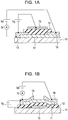
- Figs. 1A and 1B are cross-sectional views each showing an embodiment of a thin film transistor, that is, a thin film field effect transistor, according to the present invention.
- Fig. 1A is a cross-sectional view showing a top gate structure in which a gate insulating film 12 and a gate electrode 15 are formed in that order on a semiconductor channel layer 11.
- Fig. 1B is a cross-sectional showing a bottom gate structure in which the gate insulating film 12 and the semiconductor channel layer 11 are formed in that order on the gate electrode 15. From the positional relationship of the electrode and the interface between the channel layer and the insulating film, the structure shown in Fig. 1A is called a stagger structure, and that shown in Fig. 1B is called an inverted stagger structure.
- a field effect transistor having a top gate structure stagger structure
- a field effect transistor having a bottom gate structure inverted stagger structure
- the field effect transistors shown in Figs. 1A and 1B are each a three terminal device having the gate electrode 15, the source electrode 13, and the drain electrode 14.
- the above field effect transistor is an active device having a function in which a current Id flowing through the channel layer, that is, between the source electrode and the drain electrode, is controlled by applying a voltage Vg to the gate electrode.
- the TFT structure is not limited to the above structures, and any top gate or bottom gate structure, i.e., any stagger or inverted stagger structure, may also be used.
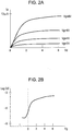
- Figs. 2A and 2B show typical properties of a field effect transistor (TFT) of the present invention.
- the properties of TFT are obtained from a field effect transistor which has the structure to be described in Example 1 and which is formed by a manufacturing method described therein.
- Vd voltage
- Vg gate voltage
- the current Id flowing between the source and the drain electrodes can be controlled (between ON and OFF).
- Fig. 2A shows the Id-Vd property at various Vg values
- Fig. 2B shows the Id-Vg property (transfer property) at a voltage Vd of 6 V.
- the channel layer of the TFT of this embodiment is formed of an amorphous oxide film containing hydrogen.
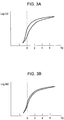
- FIGs. 3A and 3B show the TFT transistor properties obtained in comparative Example 1 and Example 1, respectively. That is, in Example 1, hydrogen was added to the channel layer, and in Comparative Example 1, hydrogen was not added to the channel layer.
- the hysteresis means that, for example, when Vg is swept (upward and downward) while Vd is fixed for evaluation of the TFT transfer property, the value of Id is different by upward sweep and downward sweep as shown in Fig. 3A .
- the hysteresis is large, when the Id value largely varies between upward sweep and downward seep at a predetermined Vg; hence, a device having a small hysteresis is preferred to control Id precisely.
- the hysteresis properties are as shown in Fig. 3A , and when the channel layer containing hydrogen according to the present invention is used, a device having a small hysteresis as shown in Fig. 3B can be obtained.
- the reason why the hysteresis is reduced when an oxide containing hydrogen is applied to the channel layer has not been clearly understood from a physical point of view.
- One estimated reason is that local structural disorder in an amorphous thin film is relaxed by addition of hydrogen, and as a result, an amorphous structure is realized in which carriers are not likely to be trapped (The number of deep traps decreases).
- the structural disorder at the interface between the channel layer and insulating film is decreased by addition of hydrogen to the channel layer and that as a result, an interface is realized between the channel layer and insulating film in which carriers are not likely to be trapped.
- Id source drain current
- Vg gate voltage
- Vd source-drain voltage
- the size of hysteresis may be evaluated by the difference between an upward-sweep Id-Vg curve and a downward-sweep Id-Vg curve.
- the area of a loop obtained from the upward-sweep Id-Vg curve and the downward-sweep Id-Vg curve may be used for this evaluation. When the area is small, it can be said that the hysteresis is small.
- this ⁇ Vt is called a threshold shift amount.
- a small ⁇ Vt indicates a small hysteresis.
- the thin-film transistor which uses an oxide containing hydrogen for its channel layer, according to the present invention, a thin-film transistor having a small ⁇ Vt can be realized.
- the threshold shift amount of the thin-film transistor of the present invention depends on a device structure, channel material, evaluation condition, and the like, for example, a voltage applied to the device is preferably set to a constant value under predetermined conditions.
- evaluation may be performed using the threshold shift amount which is obtained in the case in which Vg is swept (upward and downward) in the range of -5 to 15 V at a sweeping rate of 100 mV/sec under a constant Vg of 10 V.
- the threshold shift amount can be decreased to 2 V or less, preferably 1 V or less, and more preferably 0.5 V or less.
- the degree of required hysteresis depends on application of a thin-film transistor, a circuit structure to be used, and the like. For example, for liquid crystal display and electrophoretic display application, the requirement is relatively low; however, for organic EL display devices, arithmetic circuits, and the like, a higher degree (smaller hysteresis) is required.
- the threshold shift amount is preferably 2 V or less and more preferably 1 V or less. Furthermore, for a higher performance organic EL display device, the threshold shift amount is preferably 0.5 V or less.
- a thin film transistor having a channel layer made of an amorphous oxide was investigated.
- a semi-insulating amorphous oxide film having an electrical conductivity in the range of 0.0001 to 0.1 S/cm was favorably used as the channel layer.
- an amorphous oxide film having an electron carrier concentration of approximately 10 14 to 10 18 /cm 3 is preferably formed.
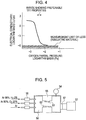
- Fig. 4 is a graph showing one example of the oxygen partial pressure dependence of the carrier concentration obtained when an In-Ga-Zn-O-based oxide thin film was formed by a sputtering method.
- a semi-insulating amorphous oxide film is obtained which has a carrier concentration of 10 14 to 10 18 /cm 3 , and when the thin film thus obtained is applied to the channel layer, a favorable TFT can be formed. As shown in Fig.
- the electron carrier concentration is controlled by addition of hydrogen (or deuterium).
- the control of the electron carrier concentration can be performed by the control of the amount of a hydrogen dopant.
- the electron carrier concentration may also be controlled by the amount of a hydrogen dopant and the amount of oxygen deficiency.
- the concentration of added hydrogen is controlled in the range of 10 16 to 10 20 /cm 3 .
- an oxide thin film can be realized which has an electron carrier concentration of approximately 10 14 to 10 18 /cm 3 and which is suitably used as the channel layer of TFT.
- the hydrogen concentration when the hydrogen concentration is set to 10 19 /cm 3 or less, the normally off operation and a large ON/OFF ratio of a transistor can be realized. Furthermore, the hydrogen concentration is preferably set to 10 17 /cm 3 or more, and by a hydrogen concentration of 10 17 /cm 3 or more, the hysteresis of a transistor can be more effectively reduced.
- the hydrogen concentration may be evaluated, for example, by secondary ion mass spectrometry (SIMS). Although depending on an evaluation apparatus, the detection limit is approximately 10 17 /cm 3 . In a region of less than the detection limit, the hydrogen concentration may be indirectly obtained by extrapolation based on the assumption of the linearity between the hydrogen concentration in a thin film and the process parameter (hydrogen partial pressure or ion implantation amount during film formation which will be described later) for addition of hydrogen.
- SIMS secondary ion mass spectrometry
- composition components of the channel layer made of an amorphous oxide containing hydrogen of the present invention and examples useful for understanding the invention are represented by the following equation (excluding the hydrogen): [(Sn 1-x M4 x )O 2 ]a ⁇ [(In 1-y M3 y ) 2 O 3 ]b ⁇ [(Zn 1-z M2 z O)]c
- composition components described above in particular, the following is an embodiment of the invention: [(In 1-y Ga y ) 2 O 3 ]b ⁇ [ZnO)]c, where 0 ⁇ y ⁇ 1, 0 ⁇ b ⁇ 1, and 0 ⁇ c ⁇ 1 hold, and the following is an example useful for understanding the invention: [(SnO 2 ]a ⁇ [(In 2 O 3 ]b ⁇ [(ZnO)]c where 0 ⁇ a ⁇ 1, 0 ⁇ b ⁇ 1, and 0 ⁇ c ⁇ 1 hold.
- the amorphous oxide film containing hydrogen can be realized by the following composition. That is, the amorphous oxide film has a secondary composition or a tertiary composition located inside a triangle having three peaks of Ga 2 O 3 , In 2 O 3 , and ZnO, or has a secondary composition or a tertiary composition located inside a triangle having three peaks of SnO 2 , In 2 O 3 , and ZnO.
- Some of tertiary compositions in a specific composition range may be crystallized in some cases. In particular, a primary composition is not preferable since it is crystallized.
- an In-Zn-O-based composition containing 20 to 70 atomic percent of In may form an amorphous film.
- an amorphous film may be formed from a composition containing 20 to 80 atomic percent of In.
- an amorphous oxide film When hydrogen atoms are added to an amorphous oxide film as described in the present invention, the amorphous film can be further stabilized at room temperature. Accordingly, an amorphous oxide can be formed in a wide tertiary composition range.
- the method (3) using ion implantation is preferable.
- the number of steps is unfavorably increased, and the distribution of hydrogen concentration is also unfavorably generated in the film thickness direction.
- the method (2) is simple as a film forming process; however, the material source containing hydrogen cannot be easily prepared, and the hydrogen concentration in the film cannot be easily controlled.
- the method (1) in which the hydrogen concentration in the film is controlled by the hydrogen partial pressure in the film-forming atmosphere the controllability is superior, and in addition, the manufacturing process is also relatively simple.
- the method (1) in which the film is formed in a gas containing hydrogen is most preferably used.
- the gas containing hydrogen used in the method (1) for example, a hydrogen gas, a deuterium gas, and a hydrocarbon gas may be mentioned.
- a hydrogen gas diluted with argon is preferably used.
- H + ions for example, H + ions, H - ions, D + ions (deuterium ions), and H 2 + ions (hydrogen molecular ions) may be mentioned.
- a vapor phase method such as a sputtering method (SP method), a pulse laser deposition method (PLD method), or an electron beam deposition method is preferably used.
- SP method sputtering method
- PLD method pulse laser deposition method
- electron beam deposition method an electron beam deposition method
- the film forming method is not limited to those mentioned above.
- the temperature of a substrate heating is not necessarily performed intentionally, so that the substrate can be maintained at approximately room temperature.
- the electron carrier concentration is controlled by the hydrogen concentration in an amorphous oxide film. Accordingly, a semi-insulating amorphous oxide film having an electron carrier concentration of 10 14 to 10 18 /cm 3 can be reproducibly obtained.
- an amorphous oxide containing hydrogen as described above is applied to the channel layer of a thin film transistor, a transistor having a small hysteresis can be reproducibly formed.
- any material may be used as long as having superior insulating properties.
- the gate insulating film 12 Al 2 O 3 , Y 2 O 3 , HfO 2 , or a mixed compound containing at least two compounds mentioned above may be used.
- the leak current between the source and the drain electrodes and that between the drain and the gate electrodes can be decreased to approximately 10 -7 A.
- any material may be used as long as having good electrical conductivity and being electrical connectable to the channel layer.
- a transparent conductive film made of In 2 O 3 :Sn, ZnO or the like or a metal film made of Au, Pt, Al, Ni or the like may be used.
- the substrate 10 for example, a glass substrate, a plastic substrate, or a plastic film may be used.
- the channel layer and the gate insulating film described above are transparent to visible light, when a transparent material is used as the materials for the above electrodes and substrate, a transparent thin film transistor can be formed.
- amorphous oxides which are applicable to the present invention, for example, there may be mentioned a Ga-In-Zn oxide, In-Zn-Ga-Mg oxide.
- the composition ratio between the constituent elements is not always required to be 1 to 1.
- the amorphous phase can be confirmed since no clear diffraction peaks are detected (that is, a hallow pattern is observed) when x-ray diffraction measurement is performed for a thin film at a low incident angle of approximately 0.5°.
- the channel layer may also contain a fine crystalline.
- a method for manufacturing an amorphous oxide film used for the channel layer of a field effect transistor comprises the following first and second steps.
- the first step is a step of disposing a substrate in a film-forming apparatus.
- the second step is a step of forming an amorphous oxide film on the substrate while a gas containing hydrogen atoms (except water vapor) and an oxygen gas are supplied in the film-forming apparatus at respective predetermined partial pressures.
- the electrical conductivity when it is intended to control the electrical conductivity and the carrier concentration only by the oxygen partial pressure, the electrical conductivity must be controlled in the narrow region in which the conductivity steeply changes depending on the oxygen partial pressure.
- the oxygen partial pressure is set to 0.008 Pa or more and preferably set to 0.01 Pa or more.
- the conductivity of the amorphous oxide films can be controlled by adjusting the partial pressure of the gas containing hydrogen atoms.
- the oxygen partial pressure dependence of the carrier concentration is not so high, for example, as compared to that in the region at an oxygen partial pressure of approximately 0.005 Pa.
- the carrier concentration can also be adjusted by hydrogen partial pressure, and in addition, since the hydrogen partial pressure dependence of the carrier concentration is low as compared to the oxygen partial pressure dependence thereof, as a result, the controllability of the film-forming atmosphere can be improved.
- the upper limit of the oxygen partial pressure is, for example, 0.1 Pa.
- the upper limit may be optionally set in the range of 0.05 to 0.5 Pa.
- the preferable hydrogen partial pressure also depends on the oxygen partial pressure, it is, for example, in the range of 0.001 to 0.01 Pa.
- water vapor is not preferably used since the control of the partial pressures of oxygen and hydrogen may become difficult in some cases.
- Hydrogen may be contained in the oxide film by addition of hydrogen in a step performed after the film formation.
- a top gate TFT shown in Fig. 1A was formed.
- the channel layer was an In-Ga-Zn-O-based amorphous oxide formed by a sputtering method in a hydrogen-containing atmosphere.
- an amorphous oxide film containing hydrogen was formed as the channel layer.
- an In-Ga-Zn-O-based amorphous oxide film containing hydrogen was formed by high-frequency sputtering in a mixed gas atmosphere containing an argon, an oxygen, and a hydrogen gas.
- reference numeral 51 indicates a sample
- reference numeral 52 a target
- reference numeral 53 a vacuum pump
- reference numeral 54 a vacuum gauge
- reference numeral 55 a substrate holder
- reference numeral 56 gas flow-rate controller provided for each gas introduction system
- reference numeral 57 a pressure controller
- reference numeral 58 a film-forming chamber.
- the vacuum pump 53 was used to evacuate the inside of the film-forming chamber 58.
- the substrate holder 55 was used to hold the substrate inside the film-forming chamber 58; the oxide film was formed on the substrate.
- the material source (the target) 52 was disposed to face the substrate holder 55. Furthermore, in the sputtering film-forming apparatus, there were provided an energy source (high-frequency electrical source, not shown) evaporating a material of the material source, means for supplying a hydrogen gas into the film-forming chamber 58, and means for supplying an oxygen gas into the film-forming chamber 58.
- an energy source high-frequency electrical source, not shown
- the gas flow-rate controllers 56 independently controlling the respective gas flow rates and the pressure controller 57 controlling the pumping speed, a predetermined gas atmosphere could be obtained in the film-forming chamber 58.
- the mixed gas of argon and oxygen and the mixed gas of argon and hydrogen were used, pure hydrogen and pure oxygen may also be used.
- the gas introduction was performed by the 3 lines for argon, the mixed gas of argon and oxygen, and the mixed gas of argon and hydrogen; however, the gas introduction may be performed by one line for a mixed gas of argon, oxygen and hydrogen or by 2 lines for a mixed gas of argon and oxygen and a mixed gas of argon and hydrogen.
- the target material source
- a 2-inch polycrystalline sintered material of InGaO 3 (ZnO) was used, and an input RF power was set to 100 W.
- the deposition rate was 12 nm/min.
- the substrate temperature was unheated and kept around room temperature of 25°C.
- spectroellipsometric measurement and analysis shows that the mean square roughness (Rrms) of the thin film was approximately 0.5 nm, and the film thickness was approximately 60 nm.
- the hydrogen concentration in the thin film was estimated to be 4 ⁇ 10 18 (1/cm 3 ).
- the electrical conductivity was approximately 10 -1 S/cm
- the electron carrier concentration and the electron mobility were estimated to be approximately 4 ⁇ 10 16 /cm 3 and 2 cm 2 /V ⁇ sec, respectively.
- the energy band gap of the amorphous oxide film thus formed was approximately 3 eV.
- the drain electrode 14 and the source electrode 13 were formed by patterning.
- the respective electrode materials were Au, and the thickness thereof was 30 nm.
- the gate insulating film 12 was formed by patterning.
- an Y 2 O 3 film having a thickness of 150 nm was formed by an electron beam deposition method.
- the relative dielectric constant of the Y 2 O 3 film was approximately 15.
- the gate electrode 15 was formed.
- the channel length and the channel width were 50 ⁇ m and 200 ⁇ m, respectively.
- the electrode material was Au, and the thickness was 30 nm.
- the channel layer When the channel layer is formed, hydrogen was not supplied, and argon and oxygen were only supplied, so that a TFT was formed.
- the total pressure was 0.4 Pa, and as the gas flow rate ratio in this case, Ar to O 2 was set to 100 to 1, so that the oxygen partial pressure was 0.004 Pa.
- the film-forming rate was 14 nm/min.
- the substrate temperature was unheated and kept around room temperature of 25°C.
- Fig. 4 is a graph showing the change in electrical conductivity of an amorphous oxide thin film as described above, which was obtained when the oxygen partial pressure was changed. As shown in the figure, in the range of the oxygen partial pressure used for TFT formation, the electrical conductivity is remarkably changed with a slight change in oxygen partial pressure; hence, the oxygen partial pressure must be accurately controlled.
- Figs. 2A and 2B are graphs each showing the current-voltage properties of a TFT, which were measured at room temperature.
- Fig. 2A shows the Id-Vd properties
- Fig. 2B shows the Id-Vg properties.
- FIG. 2A when the drain voltage Vd dependence of the current Id between the source and the drain electrodes was measured while a constant gate voltage Vg was applied, typical semiconductor transistor behavior was shown in which the Id was saturated (pinch-off) at a drain voltage Vd of approximately 6 V.
- the threshold value of the gate voltage V G at a drain voltage Vd of 4 V was approximately -0.5 V.
- the gate voltage Vg was 10 V, a current Id of approximately 1.0 ⁇ 10 -5 A flowed.
- the ON/OFF ratio of the transistor was more than 10 6 .
- a field-effect mobility of approximately 8 cm 2 (Vs) -1 was obtained in the saturated region.
- the device thus formed was irradiated with visible light and was measured in a manner similar to that described above; however, the change in transistor properties was not observed at all.
- Figs. 3A and 3B are graphs showing the Id-Vg relationships of the comparative example and this example, respectively.
- the Id-Vg relationship was one of the TFT properties. As shown in the figures, by addition of hydrogen to the channel layer, the hysteresis of the TFT can be reduced.
- the TFT can be reproducibly formed in this example, and the variation in properties of the devices thus formed tends to decrease. It is believed that since the film formation can be performed at a high oxygen partial pressure in this example as compared to that of the comparative example, the TFT can be reproducibly formed. In addition, it is also believed that since the channel layer can be formed in a hydrogen-containing atmosphere, the change in TFT properties with a slight change in oxygen partial pressure is decreased, and hence the variation in properties is decreased.
- the oxygen partial pressure was actually about 5 mPa in the comparative example and was approximately 0.015 Pa in this example.
- the oxygen partial pressure is controlled without addition of hydrogen in a sputtering method. Then, a thin film is formed having an electron carrier concentration which is suitable for the TFT channel layer.
- the oxygen partial pressure must be set to a pressure of approximately 5 mPa.
- the carrier concentration is sensitively changed with the change of the oxygen partial pressure under this condition, the properties are remarkably influenced by a slight change in film-forming condition, and as a result, it tends to be difficult to reproducibly obtain superior TFT properties.
- the electron carrier concentration is controlled by addition of hydrogen.
- a pressure of 0.01 Pa or more is used as the oxygen partial pressure.
- the film formed at this oxygen partial pressure (>0.01 Pa) without adding hydrogen is an insulating material, and hence the electron deficiency and the electron carrier concentration are sufficiently decreased.
- the film is formed in a hydrogen-containing atmosphere at a relatively high oxygen partial pressure.
- the electron mobility is decreased due to scattering between carriers and the like; however, in the amorphous oxide containing hydrogen of the present invention, as the electron carrier concentration is increased, the electron mobility is also increased. The physical mechanism of this phenomenon has not been well understood.
- the gate electrode When a voltage is applied to the gate electrode, since electrons are injected in the above amorphous oxide channel layer, current flows between the source and the drain electrodes, so that the region therebetween is put in an ON state.
- the electron mobility is increased as the electron carrier concentration is increased, the current can be further increased when the transistor is placed in an ON state. That is, the saturated current and the ON/OFF ratio can be further increased.
- the field effect transistor of the present invention having a relatively high field-effect mobility is applied, for example, to operational circuits of organic light-emitting diodes.
- an amorphous oxide film containing hydrogen will be described which is to be used for a channel layer of a thin-film transistor.
- an insulating thin film of an amorphous oxide was formed on a quartz substrate.
- a film-forming method of the amorphous oxide was performed in accordance with that described in Example 1.
- the target (material source) was InGaO 3 (ZnO), and the total pressure in an atmosphere during film formation was 0.3 Pa.
- a hydrogen gas was not supplied.
- the film thickness was set to approximately 400 nm.
- the composition analysis in the depth direction by SIMS was performed for a sample irradiated with hydrogen ions in an amount of 1 ⁇ 10 16 (1/cm 2 ), and the result is shown in Fig. 7 .
- the vertical axis (arbitrary axis) indicates the hydrogen concentration and the horizontal axis indicates the depth.
- a depth profile was obtained having a peak at approximately 200 nm deep from the surface.
- the hydrogen concentration in the thin film was approximately 2 ⁇ 10 20 (1/cm 3 ).
- the hydrogen concentration thereof is not more than the detection limit of SIMS, quantitative measurement cannot be performed; however, by the use of the above result, the hydrogen concentration can be estimated to be approximately 2 ⁇ 10 17 (1/cm 3 ).
- Fig. 6 is a graph showing the relationship between the resistivity and the amount of hydrogen ions implanted in an amorphous InGaZnO thin film.
- the horizontal axis indicates the amount of implanted hydrogen ions estimated by the method described above
- the vertical axis indicates the resistivity on a logarithm basis.
- the electrical conductivity can be controlled by addition of hydrogen to an amorphous oxide film.
- the electrical conductivity is significantly changed. That is, when hydrogen is implanted in an insulating In-Ga-Zn oxide to have a concentration of approximately 10 18 (1/cm 3 ), a semiconductor material can be obtained.
- the amount of implanted hydrogen ions is preferably set to approximately 10 18 (1/cm 3 ).
- the hydrogen content and the carrier concentration can be precisely controlled by the ion irradiation amount (irradiation time).
- the resistivity and the carrier concentration of the channel layer can be precisely controlled, and as a result, an advantage can be obtained in that devices can be reproducibly formed.
- a top gate TFT shown in Fig. 1A was formed.
- a channel layer of an amorphous oxide containing hydrogen (or deuterium) was formed by ion implantation of hydrogen or deuterium in an In-Ga-Zn-O-based amorphous oxide formed by a pulse laser deposition method (PLD method).
- PLD method pulse laser deposition method
- an In-Zn-Ga-O-based amorphous oxide film was formed by the PLD method.
- a polycrystalline sintered material of InGaO 3 (ZnO) 4 was used as the target, and an In-Zn-Ga-O-based amorphous oxide film was deposited.
- the oxygen partial pressure was 7 Pa during the film formation.
- the power of a KrF excimer laser was 1.5 ⁇ 10 -3 mJ/cm 2 /pulse, the pulse width was 20 nsec, and the repeated frequency was 10 Hz.
- the substrate temperature was unheated and kept around room temperature of 25°C.
- XRF fluorescent x-ray
- H + proton
- the acceleration voltage was 10 kV.
- Samples having various irradiation amounts in the range of 1 ⁇ 10 11 to 1 ⁇ 10 15 (1/cm 2 ) were prepared.
- samples which were ion-implanted with deuterium D + were also prepared.
- a sample irradiated with an ion amount of 2 ⁇ 10 14 (1/cm 2 ) had a hydrogen concentration of approximately 1 ⁇ 10 19 (1/cm 3 ).
- the hydrogen concentration of a sample irradiated with an ion amount of 2 ⁇ 10 12 (1/cm 2 ) is less than the detection limit, the measurement cannot be performed; however, the hydrogen concentration can be estimated to be approximately 1 ⁇ 10 17 (1/cm 3 ).
- the film was a semi-insulating film having an electrical conductivity of approximately 10 -2 S/cm.
- the drain electrode 14 and the source electrode 13 were formed by patterning.
- the respective electrode materials were Au, and the thickness thereof was 30 nm.
- the gate insulating film 12 was formed by patterning.
- a HfO 2 film having a thickness of 150 nm was formed by a laser deposition method.
- the gate electrode 15 was formed.
- the electrode material was Au, and the thickness was set to 50 nm.
- the channel length and the channel width were 50 ⁇ m and 200 ⁇ m, respectively.
- a top gate TFT shown in Fig. 1A was formed in a manner similar to that in Example 2 except for the formation of the channel layer.
- the channel layer was formed by a PLD method at an oxidation partial pressure of 6 Pa.
- ion implantation of hydrogen and deuterium was not performed. Since the oxygen partial pressure is lower than that in the example, a semi-insulating amorphous oxide film was formed because of the oxygen deficiency.
- the thin film transistor of this example showed typical semiconductor transistor behavior in which saturation (pinch-off) occurred at a voltage Vd of approximately 6 V.
- the ON/OFF ratio of the transistor was more than 10 6 , and the field-effect mobility was approximately 7 cm 2 (Vs) -1 .
- Vs cm 2
- the TFT of Example 2 had a small hysteresis as compared to that of the TFT of Comparative Example 2.
- the variation in properties in Example 2 when a plurality of devices is formed tends to be small as compared to that in Comparative Example 2. It is construed that TFTs can be reproducibly formed in this example since the film formation is performed at a higher oxygen partial pressure than that in the comparative example. In addition, it is believed that since the TFT properties are hardly changed with a slight change in oxygen partial pressure during the channel layer formation, the variation in properties among TFTs is decreased.
- the hydrogen concentration in the channel layer is low, the effect of reducing the hysteresis tends to decrease, and when the hydrogen concentration is high, the ON/OFF ratio tends to decrease.
- the hydrogen concentration is preferably set in the range of 10 17 to 10 19 (1/cm 3 ).
- the electron mobility is decreased because of scattering between carriers and the like; however, in the amorphous oxide containing hydrogen used in the present invention, with the increase in electron carrier concentration, the electron mobility is increased.
- the physical mechanism thereof has not been well understood.
- the gate electrode When a voltage is applied to the gate electrode, since electrons are injected in the above amorphous oxide channel layer, current flows between the source and the drain electrodes, so that the region therebetween is put in an ON state.
- the electron mobility is increased as the electron carrier concentration is increased, the current can be further increased when the transistor is placed in an ON state. That is, the saturated current and the ON/OFF ratio can be further increased.
- the field effect transistor of the present invention having a relatively high field-effect mobility is applied, for example, to operational circuits of organic light-emitting diodes.
- a bottom gate TFT shown in Fig. 1B was formed.
- a gate electrode of Ta having a thickness of 200 nm was formed by sputtering on a glass substrate.
- the patterning was performed by a photolithographic method and a dry etching method.
- an insulating film of a-SiN having a thickness of 250 nm was formed.
- a channel layer of an amorphous oxide containing hydrogen was formed.
- the method for forming a channel layer was performed in accordance with that of Example 1.
- a 2-inch polycrystalline sintered material of In 2 O 3 (SnO 2 ) was used, and an input RF power was set to 100 W.
- the film-forming rate was 11 nm/min.
- the substrate temperature was unheated and kept around room temperature of 25°C.
- the metal ratio of In to Sn was 0.95 to 1.
- the thin film transistor of this example showed a small hysteresis, and when a plurality of devices is formed, variation in properties tends to be small.
- the ON/OFF ratio of the transistor was more than 10 6
- the field-effect mobility was approximately 9 cm 2 (Vs) -1 .
- a top gate TFT shown in Fig. 1A was formed on a plastic substrate.
- the manufacturing method and the structure were similar to those in Example 1.
- PET polyethylene terephthalate
- the target for forming the channel layer a 2-inch polycrystalline sintered material of In 2 O 3 ⁇ ZnO was used, and an input RF power was set to 100 W.
- the film-forming rate was 12 nm/min.
- the substrate temperature was unheated and kept around room temperature of 25°C.
- the metal ratio of In to Zn was 1.1 to 0.9.
- the source electrode, the drain electrode, and the gate electrode were made of a transparent conductive film of In 2 O 3 :Sn.
- the thickness of the electrode was 100 nm.
- the thin film transistor formed on the PET film was measured at room temperature.
- the ON/OFF ratio of the transistor was more than 10 3 .
- the field-effect mobility was calculated, it was approximately 3 cm 2 (Vs) -1 .
- the transistor properties as described above were also evaluated, a significant change in transistor properties was not observed.
- irradiation of visible light was performed and the measurement as described above was performed, the change in transistor properties was not observed.
- the thin film transistor formed in this example was transparent to visible light and was formed on a flexible substrate.
- the above field effect transistor can be formed on a flexible material such as a PET film. That is, switching can be performed while this transistor is being bent, and the transistor is transparent to visible and infrared light having a wavelength of 400 nm or more (in this case, the transistor is not required to have a light transmission of 100% but may be required to be practically transparent).
- the field effect transistor may be used as a switching device of LCD and/or organic EL display devices.
- the field effect transistor of the present invention may also be widely used, for example, for see-through displays, IC cards, and ID tags besides flexible displays.
- the amorphous oxide containing hydrogen (or deuterium) is applied to the channel layer of a field effect transistor, a thin film field effect transistor having a small hysteresis can be realized.
- the film formation is performed in an atmosphere containing a hydrogen gas and an oxygen gas, the carrier concentration of an amorphous oxide can be highly accurately controlled.
- a low temperature process can be performed, and hence the field effect transistor can be formed on a substrate such as a plastic plate or film.
- the field effect transistor can be reproducibly formed.
- the amorphous oxide having a low electron carrier concentration can be formed with good control.
Landscapes
- Thin Film Transistor (AREA)
- Dram (AREA)
Applications Claiming Priority (3)
| Application Number | Priority Date | Filing Date | Title |
|---|---|---|---|
| JP2005258263 | 2005-09-06 | ||
| JP2006221552A JP4560502B2 (ja) | 2005-09-06 | 2006-08-15 | 電界効果型トランジスタ |
| EP06797762A EP1915784A1 (en) | 2005-09-06 | 2006-09-05 | Field effect transistor using amorphous oxide film as channel layer, manufacturing method of field effect transistor using amorphous oxide film as channel layer, and manufacturing method of amorphous oxide film |
Related Parent Applications (1)
| Application Number | Title | Priority Date | Filing Date |
|---|---|---|---|
| EP06797762A Division EP1915784A1 (en) | 2005-09-06 | 2006-09-05 | Field effect transistor using amorphous oxide film as channel layer, manufacturing method of field effect transistor using amorphous oxide film as channel layer, and manufacturing method of amorphous oxide film |
Publications (2)
| Publication Number | Publication Date |
|---|---|
| EP2816607A1 EP2816607A1 (en) | 2014-12-24 |
| EP2816607B1 true EP2816607B1 (en) | 2017-11-15 |
Family
ID=37460356
Family Applications (3)
| Application Number | Title | Priority Date | Filing Date |
|---|---|---|---|
| EP14184889.5A Active EP2816607B1 (en) | 2005-09-06 | 2006-09-05 | Field effect transistor using amorphous oxide film as channel layer |
| EP06797762A Withdrawn EP1915784A1 (en) | 2005-09-06 | 2006-09-05 | Field effect transistor using amorphous oxide film as channel layer, manufacturing method of field effect transistor using amorphous oxide film as channel layer, and manufacturing method of amorphous oxide film |
| EP11161456.6A Not-in-force EP2339639B1 (en) | 2005-09-06 | 2006-09-05 | Field effect transistor using amorphous oxide film as channel layer |
Family Applications After (2)
| Application Number | Title | Priority Date | Filing Date |
|---|---|---|---|
| EP06797762A Withdrawn EP1915784A1 (en) | 2005-09-06 | 2006-09-05 | Field effect transistor using amorphous oxide film as channel layer, manufacturing method of field effect transistor using amorphous oxide film as channel layer, and manufacturing method of amorphous oxide film |
| EP11161456.6A Not-in-force EP2339639B1 (en) | 2005-09-06 | 2006-09-05 | Field effect transistor using amorphous oxide film as channel layer |
Country Status (6)
| Country | Link |
|---|---|
| US (4) | US7791074B2 (enExample) |
| EP (3) | EP2816607B1 (enExample) |
| JP (1) | JP4560502B2 (enExample) |
| KR (1) | KR101051204B1 (enExample) |
| CN (2) | CN102496577B (enExample) |
| WO (1) | WO2007029844A1 (enExample) |
Families Citing this family (326)
| Publication number | Priority date | Publication date | Assignee | Title |
|---|---|---|---|---|
| EP1737044B1 (en) * | 2004-03-12 | 2014-12-10 | Japan Science and Technology Agency | Amorphous oxide and thin film transistor |
| CN102945857B (zh) * | 2004-11-10 | 2015-06-03 | 佳能株式会社 | 无定形氧化物和场效应晶体管 |
| CN101258607B (zh) * | 2005-09-06 | 2011-01-05 | 佳能株式会社 | 使用非晶氧化物膜作为沟道层的场效应晶体管、使用非晶氧化物膜作为沟道层的场效应晶体管的制造方法、以及非晶氧化物膜的制造方法 |
| JP4560502B2 (ja) | 2005-09-06 | 2010-10-13 | キヤノン株式会社 | 電界効果型トランジスタ |
| JP5058469B2 (ja) * | 2005-09-06 | 2012-10-24 | キヤノン株式会社 | スパッタリングターゲットおよび該ターゲットを用いた薄膜の形成方法 |
| JP5099740B2 (ja) * | 2005-12-19 | 2012-12-19 | 財団法人高知県産業振興センター | 薄膜トランジスタ |
| JP5110803B2 (ja) | 2006-03-17 | 2012-12-26 | キヤノン株式会社 | 酸化物膜をチャネルに用いた電界効果型トランジスタ及びその製造方法 |
| KR100982395B1 (ko) * | 2007-04-25 | 2010-09-14 | 주식회사 엘지화학 | 박막 트랜지스터 및 이의 제조방법 |
| JPWO2008139860A1 (ja) * | 2007-05-07 | 2010-07-29 | 出光興産株式会社 | 半導体薄膜、半導体薄膜の製造方法、および、半導体素子 |
| US8803781B2 (en) * | 2007-05-18 | 2014-08-12 | Semiconductor Energy Laboratory Co., Ltd. | Semiconductor device and display device |
| US9434642B2 (en) | 2007-05-21 | 2016-09-06 | Corning Incorporated | Mechanically flexible and durable substrates |
| KR101092483B1 (ko) * | 2007-05-31 | 2011-12-13 | 캐논 가부시끼가이샤 | 산화물 반도체를 사용한 박막트랜지스터의 제조 방법 |
| KR101238926B1 (ko) * | 2007-12-28 | 2013-03-06 | 가부시키가이샤 아루박 | 투명 도전막의 성막 방법 및 성막 장치 |
| JP5219529B2 (ja) | 2008-01-23 | 2013-06-26 | キヤノン株式会社 | 電界効果型トランジスタ及び、該電界効果型トランジスタを備えた表示装置 |
| JP2009206508A (ja) * | 2008-01-31 | 2009-09-10 | Canon Inc | 薄膜トランジスタ及び表示装置 |
| KR100963026B1 (ko) * | 2008-06-30 | 2010-06-10 | 삼성모바일디스플레이주식회사 | 박막 트랜지스터, 그의 제조 방법 및 박막 트랜지스터를구비하는 평판 표시 장치 |
| CN105575803B (zh) * | 2008-08-15 | 2018-11-09 | 株式会社爱发科 | 场效应晶体管的制造方法 |
| US8129718B2 (en) | 2008-08-28 | 2012-03-06 | Canon Kabushiki Kaisha | Amorphous oxide semiconductor and thin film transistor using the same |
| JP5430113B2 (ja) * | 2008-10-08 | 2014-02-26 | キヤノン株式会社 | 電界効果型トランジスタ及びその製造方法 |
| CN102187467A (zh) | 2008-10-23 | 2011-09-14 | 出光兴产株式会社 | 薄膜晶体管及其制造方法 |
| JP5616012B2 (ja) * | 2008-10-24 | 2014-10-29 | 株式会社半導体エネルギー研究所 | 半導体装置の作製方法 |
| JP5442234B2 (ja) * | 2008-10-24 | 2014-03-12 | 株式会社半導体エネルギー研究所 | 半導体装置及び表示装置 |
| CN103456794B (zh) | 2008-12-19 | 2016-08-10 | 株式会社半导体能源研究所 | 晶体管的制造方法 |
| WO2010074927A2 (en) * | 2008-12-24 | 2010-07-01 | 3M Innovative Properties Company | Stability enhancements in metal oxide semiconductor thin film transistors |
| EP2202802B1 (en) | 2008-12-24 | 2012-09-26 | Semiconductor Energy Laboratory Co., Ltd. | Driver circuit and semiconductor device |
| TWI474408B (zh) | 2008-12-26 | 2015-02-21 | 半導體能源研究所股份有限公司 | 半導體裝置及其製造方法 |
| US8174021B2 (en) * | 2009-02-06 | 2012-05-08 | Semiconductor Energy Laboratory Co., Ltd. | Semiconductor device and method of manufacturing the semiconductor device |
| JP5504008B2 (ja) | 2009-03-06 | 2014-05-28 | 株式会社半導体エネルギー研究所 | 半導体装置 |
| KR102342672B1 (ko) * | 2009-03-12 | 2021-12-24 | 가부시키가이샤 한도오따이 에네루기 켄큐쇼 | 반도체 장치 |
| KR101681884B1 (ko) | 2009-03-27 | 2016-12-05 | 가부시키가이샤 한도오따이 에네루기 켄큐쇼 | 반도체장치, 표시장치 및 전자기기 |
| US8338226B2 (en) * | 2009-04-02 | 2012-12-25 | Semiconductor Energy Laboratory Co., Ltd. | Method for manufacturing semiconductor device |
| EP2256814B1 (en) * | 2009-05-29 | 2019-01-16 | Semiconductor Energy Laboratory Co, Ltd. | Oxide semiconductor device and method for manufacturing the same |
| JP5564331B2 (ja) * | 2009-05-29 | 2014-07-30 | 株式会社半導体エネルギー研究所 | 半導体装置の作製方法 |
| US8865516B2 (en) * | 2009-06-29 | 2014-10-21 | Sharp Kabushiki Kaisha | Oxide semiconductor, thin film transistor array substrate and production method thereof, and display device |
| CN104576748B (zh) | 2009-06-30 | 2019-03-15 | 株式会社半导体能源研究所 | 半导体装置的制造方法 |
| KR101457837B1 (ko) | 2009-06-30 | 2014-11-05 | 가부시키가이샤 한도오따이 에네루기 켄큐쇼 | 반도체 장치 제작 방법 |
| EP2449594B1 (en) * | 2009-06-30 | 2019-08-21 | Semiconductor Energy Laboratory Co., Ltd. | Method for manufacturing semiconductor device |
| JP5478165B2 (ja) * | 2009-06-30 | 2014-04-23 | 株式会社半導体エネルギー研究所 | 半導体装置 |
| JP5640478B2 (ja) * | 2009-07-09 | 2014-12-17 | 株式会社リコー | 電界効果型トランジスタの製造方法及び電界効果型トランジスタ |
| WO2011007677A1 (en) * | 2009-07-17 | 2011-01-20 | Semiconductor Energy Laboratory Co., Ltd. | Semiconductor device and method for manufacturing the same |
| WO2011007682A1 (en) | 2009-07-17 | 2011-01-20 | Semiconductor Energy Laboratory Co., Ltd. | Method of manufacturing semiconductor device |
| KR102057221B1 (ko) * | 2009-09-16 | 2019-12-18 | 가부시키가이샤 한도오따이 에네루기 켄큐쇼 | 반도체 장치 및 그 제조 방법 |
| KR101519893B1 (ko) * | 2009-09-16 | 2015-05-14 | 가부시키가이샤 한도오따이 에네루기 켄큐쇼 | 트랜지스터 |
| CN102576677B (zh) * | 2009-09-24 | 2015-07-22 | 株式会社半导体能源研究所 | 半导体元件及其制造方法 |
| WO2011039853A1 (ja) | 2009-09-30 | 2011-04-07 | キヤノン株式会社 | 薄膜トランジスタ |
| WO2011043163A1 (en) | 2009-10-05 | 2011-04-14 | Semiconductor Energy Laboratory Co., Ltd. | Semiconductor device and manufacturing method thereof |
| WO2011043206A1 (en) * | 2009-10-09 | 2011-04-14 | Semiconductor Energy Laboratory Co., Ltd. | Semiconductor device |
| KR101820972B1 (ko) | 2009-10-09 | 2018-01-22 | 가부시키가이샤 한도오따이 에네루기 켄큐쇼 | 반도체 장치 및 그 제조 방법 |
| CN110061144A (zh) | 2009-10-16 | 2019-07-26 | 株式会社半导体能源研究所 | 逻辑电路和半导体器件 |
| KR101865546B1 (ko) * | 2009-10-16 | 2018-06-11 | 가부시키가이샤 한도오따이 에네루기 켄큐쇼 | 액정 표시 장치 및 액정 표시 장치를 포함한 전자 기기 |
| WO2011046015A1 (en) | 2009-10-16 | 2011-04-21 | Semiconductor Energy Laboratory Co., Ltd. | Logic circuit and semiconductor device |
| WO2011046048A1 (en) * | 2009-10-16 | 2011-04-21 | Semiconductor Energy Laboratory Co., Ltd. | Semiconductor device and manufacturing method thereof |
| CN116722019A (zh) | 2009-10-16 | 2023-09-08 | 株式会社半导体能源研究所 | 显示设备 |
| KR101847656B1 (ko) * | 2009-10-21 | 2018-05-24 | 가부시키가이샤 한도오따이 에네루기 켄큐쇼 | 반도체 장치 및 그 제조 방법 |
| WO2011048923A1 (en) * | 2009-10-21 | 2011-04-28 | Semiconductor Energy Laboratory Co., Ltd. | E-book reader |
| KR102223581B1 (ko) | 2009-10-21 | 2021-03-04 | 가부시키가이샤 한도오따이 에네루기 켄큐쇼 | 아날로그 회로 및 반도체 장치 |
| CN102598280B (zh) * | 2009-10-21 | 2016-05-18 | 株式会社半导体能源研究所 | 液晶显示器件及包括该液晶显示器件的电子设备 |
| CN104485336B (zh) | 2009-10-21 | 2018-01-02 | 株式会社半导体能源研究所 | 半导体器件 |
| CN105070715B (zh) * | 2009-10-21 | 2018-10-19 | 株式会社半导体能源研究所 | 半导体装置 |
| WO2011049230A1 (en) * | 2009-10-21 | 2011-04-28 | Semiconductor Energy Laboratory Co., Ltd. | Voltage regulator circuit |
| KR20120096463A (ko) * | 2009-10-21 | 2012-08-30 | 가부시키가이샤 한도오따이 에네루기 켄큐쇼 | 표시 장치 및 표시 장치를 갖는 전자 기기 |
| EP2494594B1 (en) * | 2009-10-29 | 2020-02-19 | Semiconductor Energy Laboratory Co. Ltd. | Semiconductor device |
| KR102416955B1 (ko) * | 2009-10-29 | 2022-07-05 | 가부시키가이샤 한도오따이 에네루기 켄큐쇼 | 반도체 장치 |
| KR20120091243A (ko) | 2009-10-30 | 2012-08-17 | 가부시키가이샤 한도오따이 에네루기 켄큐쇼 | 반도체 장치 |
| WO2011052413A1 (en) * | 2009-10-30 | 2011-05-05 | Semiconductor Energy Laboratory Co., Ltd. | Non-linear element, display device, and electronic device |
| KR101740684B1 (ko) * | 2009-10-30 | 2017-05-26 | 가부시키가이샤 한도오따이 에네루기 켄큐쇼 | 파워 다이오드, 정류기 및 그것을 가지는 반도체 장치 |
| WO2011052409A1 (en) * | 2009-10-30 | 2011-05-05 | Semiconductor Energy Laboratory Co., Ltd. | Transistor |
| WO2011052383A1 (en) * | 2009-10-30 | 2011-05-05 | Semiconductor Energy Laboratory Co., Ltd. | Logic circuit and semiconductor device |
| WO2011052411A1 (en) * | 2009-10-30 | 2011-05-05 | Semiconductor Energy Laboratory Co., Ltd. | Transistor |
| CN102668096B (zh) * | 2009-10-30 | 2015-04-29 | 株式会社半导体能源研究所 | 半导体装置及其制造方法 |
| KR102062077B1 (ko) * | 2009-10-30 | 2020-01-03 | 가부시키가이샤 한도오따이 에네루기 켄큐쇼 | 반도체 장치 |
| EP2494597A4 (en) * | 2009-10-30 | 2015-03-18 | Semiconductor Energy Lab | SEMICONDUCTOR COMPONENT |
| KR101835155B1 (ko) * | 2009-10-30 | 2018-03-06 | 가부시키가이샤 한도오따이 에네루기 켄큐쇼 | 액정 표시 장치, 액정 표시 장치의 구동 방법 및 액정 표시 장치를 포함하는 전자 기기 |
| WO2011052437A1 (en) * | 2009-10-30 | 2011-05-05 | Semiconductor Energy Laboratory Co., Ltd. | Non-linear element, display device including non-linear element, and electronic device including display device |
| KR101788521B1 (ko) | 2009-10-30 | 2017-10-19 | 가부시키가이샤 한도오따이 에네루기 켄큐쇼 | 반도체 장치 |
| KR101861980B1 (ko) | 2009-11-06 | 2018-05-28 | 가부시키가이샤 한도오따이 에네루기 켄큐쇼 | 반도체 장치 |
| EP2497011A4 (en) * | 2009-11-06 | 2013-10-02 | Semiconductor Energy Lab | TOUCH PANEL AND METHOD FOR CONTROLLING TOUCH PANEL |
| KR101810254B1 (ko) | 2009-11-06 | 2017-12-18 | 가부시키가이샤 한도오따이 에네루기 켄큐쇼 | 반도체 장치 및 그 동작 방법 |
| WO2011055638A1 (en) | 2009-11-06 | 2011-05-12 | Semiconductor Energy Laboratory Co., Ltd. | Display device |
| CN104393007A (zh) | 2009-11-06 | 2015-03-04 | 株式会社半导体能源研究所 | 半导体装置 |
| EP2497115A4 (en) | 2009-11-06 | 2015-09-02 | Semiconductor Energy Lab | SEMICONDUCTOR COMPONENT AND MANUFACTURING METHOD THEREFOR |
| CN102612741B (zh) * | 2009-11-06 | 2014-11-12 | 株式会社半导体能源研究所 | 半导体装置 |
| KR101930230B1 (ko) | 2009-11-06 | 2018-12-18 | 가부시키가이샤 한도오따이 에네루기 켄큐쇼 | 반도체 장치를 제작하기 위한 방법 |
| WO2011058913A1 (en) * | 2009-11-13 | 2011-05-19 | Semiconductor Energy Laboratory Co., Ltd. | Semiconductor device and manufacturing method thereof |
| KR102450568B1 (ko) | 2009-11-13 | 2022-10-07 | 가부시키가이샤 한도오따이 에네루기 켄큐쇼 | 반도체 장치 및 그 제작 방법 |
| CN105655351B (zh) * | 2009-11-13 | 2019-11-01 | 株式会社半导体能源研究所 | 显示器件 |
| KR101893332B1 (ko) * | 2009-11-13 | 2018-08-31 | 가부시키가이샤 한도오따이 에네루기 켄큐쇼 | 반도체 장치 및 반도체 장치의 구동 방법 |
| CN102668097B (zh) * | 2009-11-13 | 2015-08-12 | 株式会社半导体能源研究所 | 半导体器件及其制造方法 |
| WO2011058864A1 (en) * | 2009-11-13 | 2011-05-19 | Semiconductor Energy Laboratory Co., Ltd. | Device including nonvolatile memory element |
| JP5656325B2 (ja) * | 2009-11-13 | 2015-01-21 | 株式会社半導体エネルギー研究所 | 非線形素子、及び表示装置 |
| KR20120094013A (ko) * | 2009-11-13 | 2012-08-23 | 가부시키가이샤 한도오따이 에네루기 켄큐쇼 | 스퍼터링 타겟 및 그 제조방법, 및 트랜지스터 |
| WO2011062029A1 (en) * | 2009-11-18 | 2011-05-26 | Semiconductor Energy Laboratory Co., Ltd. | Memory device |
| WO2011062041A1 (en) * | 2009-11-20 | 2011-05-26 | Semiconductor Energy Laboratory Co., Ltd. | Transistor |
| KR101995704B1 (ko) | 2009-11-20 | 2019-07-03 | 가부시키가이샤 한도오따이 에네루기 켄큐쇼 | 반도체 장치의 제작 방법 |
| WO2011062057A1 (en) * | 2009-11-20 | 2011-05-26 | Semiconductor Energy Laboratory Co., Ltd. | Semiconductor device |
| KR102682982B1 (ko) | 2009-11-20 | 2024-07-10 | 가부시키가이샤 한도오따이 에네루기 켄큐쇼 | 반도체 장치 |
| WO2011062075A1 (en) | 2009-11-20 | 2011-05-26 | Semiconductor Energy Laboratory Co., Ltd. | Nonvolatile latch circuit and logic circuit, and semiconductor device using the same |
| KR101448908B1 (ko) * | 2009-11-20 | 2014-10-15 | 가부시키가이샤 한도오따이 에네루기 켄큐쇼 | 반도체 장치 |
| KR20120107079A (ko) | 2009-11-20 | 2012-09-28 | 가부시키가이샤 한도오따이 에네루기 켄큐쇼 | 박막 트랜지스터 |
| KR101829176B1 (ko) * | 2009-11-20 | 2018-02-13 | 가부시키가이샤 한도오따이 에네루기 켄큐쇼 | 반도체 장치 |
| JP5762723B2 (ja) | 2009-11-20 | 2015-08-12 | 株式会社半導体エネルギー研究所 | 変調回路及びそれを備えた半導体装置 |
| CN102668063B (zh) * | 2009-11-20 | 2015-02-18 | 株式会社半导体能源研究所 | 半导体装置 |
| JP5657878B2 (ja) * | 2009-11-20 | 2015-01-21 | 株式会社半導体エネルギー研究所 | トランジスタの作製方法 |
| WO2011065183A1 (en) * | 2009-11-24 | 2011-06-03 | Semiconductor Energy Laboratory Co., Ltd. | Semiconductor device including memory cell |
| WO2011065209A1 (en) | 2009-11-27 | 2011-06-03 | Semiconductor Energy Laboratory Co., Ltd. | Non-linear element, display device including non-linear element, and electronic device including display device |
| KR102614462B1 (ko) | 2009-11-27 | 2023-12-14 | 가부시키가이샤 한도오따이 에네루기 켄큐쇼 | 반도체 장치 및 반도체 장치의 제작방법 |
| CN102640293B (zh) * | 2009-11-27 | 2015-07-22 | 株式会社半导体能源研究所 | 半导体器件 |
| WO2011065258A1 (en) * | 2009-11-27 | 2011-06-03 | Semiconductor Energy Laboratory Co., Ltd. | Semiconductor device |
| CN105206514B (zh) | 2009-11-28 | 2018-04-10 | 株式会社半导体能源研究所 | 层叠的氧化物材料、半导体器件、以及用于制造该半导体器件的方法 |
| WO2011065210A1 (en) | 2009-11-28 | 2011-06-03 | Semiconductor Energy Laboratory Co., Ltd. | Stacked oxide material, semiconductor device, and method for manufacturing the semiconductor device |
| KR20190100462A (ko) | 2009-11-28 | 2019-08-28 | 가부시키가이샤 한도오따이 에네루기 켄큐쇼 | 반도체 장치 및 그 제조 방법 |
| CN102648490B (zh) | 2009-11-30 | 2016-08-17 | 株式会社半导体能源研究所 | 液晶显示设备、用于驱动该液晶显示设备的方法、以及包括该液晶显示设备的电子设备 |
| KR101464776B1 (ko) * | 2009-12-01 | 2014-11-25 | 엘지디스플레이 주식회사 | 탄소나노튜브 분산액, 이를 이용한 박막 및 표시장치의 제조방법 |
| KR101840623B1 (ko) * | 2009-12-04 | 2018-03-21 | 가부시키가이샤 한도오따이 에네루기 켄큐쇼 | 표시 장치 및 이를 포함하는 전자 기기 |
| WO2011068028A1 (en) | 2009-12-04 | 2011-06-09 | Semiconductor Energy Laboratory Co., Ltd. | Semiconductor element, semiconductor device, and method for manufacturing the same |
| KR20120103676A (ko) | 2009-12-04 | 2012-09-19 | 가부시키가이샤 한도오따이 에네루기 켄큐쇼 | 반도체 장치 |
| KR20120107107A (ko) | 2009-12-04 | 2012-09-28 | 가부시키가이샤 한도오따이 에네루기 켄큐쇼 | 반도체 장치 |
| KR101963300B1 (ko) | 2009-12-04 | 2019-03-28 | 가부시키가이샤 한도오따이 에네루기 켄큐쇼 | 표시 장치 |
| WO2011068021A1 (en) * | 2009-12-04 | 2011-06-09 | Semiconductor Energy Laboratory Co., Ltd. | Display device |
| KR102450889B1 (ko) | 2009-12-04 | 2022-10-06 | 가부시키가이샤 한도오따이 에네루기 켄큐쇼 | 반도체 장치 |
| WO2011068025A1 (en) * | 2009-12-04 | 2011-06-09 | Semiconductor Energy Laboratory Co., Ltd. | Dc converter circuit and power supply circuit |
| WO2011070892A1 (en) | 2009-12-08 | 2011-06-16 | Semiconductor Energy Laboratory Co., Ltd. | Semiconductor device and manufacturing method thereof |
| IN2012DN04871A (enExample) | 2009-12-11 | 2015-09-25 | Semiconductor Energy Laoboratory Co Ltd | |
| KR20170116239A (ko) * | 2009-12-11 | 2017-10-18 | 가부시키가이샤 한도오따이 에네루기 켄큐쇼 | 전계 효과 트랜지스터 |
| JP5727204B2 (ja) * | 2009-12-11 | 2015-06-03 | 株式会社半導体エネルギー研究所 | 半導体装置の作製方法 |
| KR102046308B1 (ko) | 2009-12-11 | 2019-11-19 | 가부시키가이샤 한도오따이 에네루기 켄큐쇼 | 반도체 장치 |
| KR101765849B1 (ko) | 2009-12-18 | 2017-08-08 | 가부시키가이샤 한도오따이 에네루기 켄큐쇼 | 액정 표시 장치 및 전자 기기 |
| KR101743620B1 (ko) | 2009-12-18 | 2017-06-05 | 가부시키가이샤 한도오따이 에네루기 켄큐쇼 | 광 센서를 포함하는 표시 장치 및 그 구동 방법 |
| WO2011074409A1 (en) * | 2009-12-18 | 2011-06-23 | Semiconductor Energy Laboratory Co., Ltd. | Method for manufacturing semiconductor device |
| KR101481399B1 (ko) * | 2009-12-18 | 2015-01-14 | 가부시키가이샤 한도오따이 에네루기 켄큐쇼 | 반도체 장치 |
| CN102656625B (zh) * | 2009-12-18 | 2016-08-03 | 株式会社半导体能源研究所 | 用于驱动液晶显示设备的方法 |
| WO2011074407A1 (en) * | 2009-12-18 | 2011-06-23 | Semiconductor Energy Laboratory Co., Ltd. | Semiconductor device and method for manufacturing the same |
| CN104700890B (zh) * | 2009-12-18 | 2017-10-17 | 株式会社半导体能源研究所 | 非易失性锁存电路和逻辑电路以及使用它们的半导体器件 |
| KR101900662B1 (ko) * | 2009-12-18 | 2018-11-08 | 가부시키가이샤 한도오따이 에네루기 켄큐쇼 | 액정 표시 장치 및 그 구동 방법 |
| WO2011077926A1 (en) * | 2009-12-24 | 2011-06-30 | Semiconductor Energy Laboratory Co., Ltd. | Display device and electronic device |
| CN102656801B (zh) * | 2009-12-25 | 2016-04-27 | 株式会社半导体能源研究所 | 存储器装置、半导体器件和电子装置 |
| KR101613701B1 (ko) * | 2009-12-25 | 2016-04-19 | 가부시키가이샤 한도오따이 에네루기 켄큐쇼 | 액정 표시 장치의 구동 방법 |
| KR101811203B1 (ko) * | 2009-12-25 | 2017-12-22 | 가부시키가이샤 한도오따이 에네루기 켄큐쇼 | 반도체 장치 및 이를 제작하기 위한 방법 |
| KR102167820B1 (ko) | 2009-12-25 | 2020-10-20 | 가부시키가이샤 한도오따이 에네루기 켄큐쇼 | 메모리 장치 |
| KR101434948B1 (ko) * | 2009-12-25 | 2014-08-28 | 가부시키가이샤 한도오따이 에네루기 켄큐쇼 | 반도체 장치 |
| KR20250156859A (ko) * | 2009-12-28 | 2025-11-03 | 가부시키가이샤 한도오따이 에네루기 켄큐쇼 | 기억 장치와 반도체 장치 |
| EP2519969A4 (en) * | 2009-12-28 | 2016-07-06 | Semiconductor Energy Lab | SEMICONDUCTOR COMPONENT |
| KR101749944B1 (ko) | 2009-12-28 | 2017-06-22 | 가부시키가이샤 한도오따이 에네루기 켄큐쇼 | 액정 표시 장치 및 전자 기기 |
| KR101842413B1 (ko) * | 2009-12-28 | 2018-03-26 | 가부시키가이샤 한도오따이 에네루기 켄큐쇼 | 반도체 장치 |
| US8780629B2 (en) * | 2010-01-15 | 2014-07-15 | Semiconductor Energy Laboratory Co., Ltd. | Semiconductor device and driving method thereof |
| WO2011086847A1 (en) * | 2010-01-15 | 2011-07-21 | Semiconductor Energy Laboratory Co., Ltd. | Semiconductor device |
| KR101791279B1 (ko) * | 2010-01-15 | 2017-10-27 | 가부시키가이샤 한도오따이 에네루기 켄큐쇼 | 반도체 장치 |
| CN102725841B (zh) * | 2010-01-15 | 2016-10-05 | 株式会社半导体能源研究所 | 半导体器件 |
| KR101848516B1 (ko) * | 2010-01-15 | 2018-04-12 | 가부시키가이샤 한도오따이 에네루기 켄큐쇼 | 반도체 장치 |
| WO2011089842A1 (en) | 2010-01-20 | 2011-07-28 | Semiconductor Energy Laboratory Co., Ltd. | Driving method of liquid crystal display device |
| KR101842860B1 (ko) | 2010-01-20 | 2018-03-28 | 가부시키가이샤 한도오따이 에네루기 켄큐쇼 | 표시 장치의 구동 방법 |
| WO2011089847A1 (en) | 2010-01-20 | 2011-07-28 | Semiconductor Energy Laboratory Co., Ltd. | Signal processing circuit and method for driving the same |
| KR102248998B1 (ko) | 2010-01-20 | 2021-05-07 | 가부시키가이샤 한도오따이 에네루기 켄큐쇼 | 전자 기기 |
| KR101978106B1 (ko) * | 2010-01-20 | 2019-05-13 | 가부시키가이샤 한도오따이 에네루기 켄큐쇼 | 반도체 장치 |
| US8415731B2 (en) * | 2010-01-20 | 2013-04-09 | Semiconductor Energy Laboratory Co., Ltd. | Semiconductor storage device with integrated capacitor and having transistor overlapping sections |
| KR101787734B1 (ko) * | 2010-01-20 | 2017-10-18 | 가부시키가이샤 한도오따이 에네루기 켄큐쇼 | 반도체 기억 장치 |
| KR101773641B1 (ko) | 2010-01-22 | 2017-09-12 | 가부시키가이샤 한도오따이 에네루기 켄큐쇼 | 반도체 장치 |
| CN102714026B (zh) * | 2010-01-24 | 2016-09-14 | 株式会社半导体能源研究所 | 显示装置 |
| KR101805378B1 (ko) | 2010-01-24 | 2017-12-06 | 가부시키가이샤 한도오따이 에네루기 켄큐쇼 | 표시 장치와 이의 제조 방법 |
| WO2011093003A1 (en) * | 2010-01-29 | 2011-08-04 | Semiconductor Energy Laboratory Co., Ltd. | Semiconductor memory device |
| KR101921618B1 (ko) * | 2010-02-05 | 2018-11-26 | 가부시키가이샤 한도오따이 에네루기 켄큐쇼 | 반도체 장치 및 반도체 장치의 구동 방법 |
| WO2011096270A1 (en) | 2010-02-05 | 2011-08-11 | Semiconductor Energy Laboratory Co., Ltd. | Semiconductor device |
| KR101862823B1 (ko) * | 2010-02-05 | 2018-05-30 | 가부시키가이샤 한도오따이 에네루기 켄큐쇼 | 반도체 장치 및 반도체 장치의 구동 방법 |
| KR101926336B1 (ko) * | 2010-02-05 | 2019-03-07 | 가부시키가이샤 한도오따이 에네루기 켄큐쇼 | 반도체 장치 |
| WO2011096286A1 (en) * | 2010-02-05 | 2011-08-11 | Semiconductor Energy Laboratory Co., Ltd. | Field effect transistor and semiconductor device |
| US8617920B2 (en) * | 2010-02-12 | 2013-12-31 | Semiconductor Energy Laboratory Co., Ltd. | Semiconductor device and manufacturing method thereof |
| KR101775180B1 (ko) | 2010-02-12 | 2017-09-05 | 가부시키가이샤 한도오따이 에네루기 켄큐쇼 | 반도체 장치 및 그 구동 방법 |
| EP2534679B1 (en) | 2010-02-12 | 2021-06-16 | Semiconductor Energy Laboratory Co., Ltd. | Semiconductor device and driving method of the same |
| WO2011099368A1 (en) | 2010-02-12 | 2011-08-18 | Semiconductor Energy Laboratory Co., Ltd. | Semiconductor device and display device including the same |
| JP5569780B2 (ja) * | 2010-02-18 | 2014-08-13 | 国立大学法人東京農工大学 | 薄膜トランジスタの製造方法 |
| CN102763214B (zh) | 2010-02-19 | 2015-02-18 | 株式会社半导体能源研究所 | 半导体器件 |
| CN102754163B (zh) * | 2010-02-19 | 2015-11-25 | 株式会社半导体能源研究所 | 半导体器件 |
| CN102763332B (zh) * | 2010-02-23 | 2016-04-13 | 株式会社半导体能源研究所 | 显示装置、半导体装置以及它们的驱动方法 |
| CN102754022B (zh) | 2010-02-26 | 2016-11-09 | 株式会社半导体能源研究所 | 液晶显示装置 |
| WO2011105310A1 (en) * | 2010-02-26 | 2011-09-01 | Semiconductor Energy Laboratory Co., Ltd. | Semiconductor device |
| KR101862811B1 (ko) | 2010-02-26 | 2018-05-30 | 가부시키가이샤 한도오따이 에네루기 켄큐쇼 | 표시장치 및 표시장치의 구동 방법 |
| WO2011105198A1 (en) * | 2010-02-26 | 2011-09-01 | Semiconductor Energy Laboratory Co., Ltd. | Semiconductor device |
| KR102341927B1 (ko) * | 2010-03-05 | 2021-12-23 | 가부시키가이샤 한도오따이 에네루기 켄큐쇼 | 표시 장치 |
| WO2011108346A1 (en) * | 2010-03-05 | 2011-09-09 | Semiconductor Energy Laboratory Co., Ltd. | Manufacturing method of oxide semiconductor film and manufacturing method of transistor |
| KR102220018B1 (ko) | 2010-03-08 | 2021-02-26 | 가부시키가이샤 한도오따이 에네루기 켄큐쇼 | 반도체 장치 및 반도체 장치를 제작하는 방법 |
| DE112011100840T5 (de) * | 2010-03-08 | 2013-01-17 | Semiconductor Energy Laboratory Co., Ltd. | Anzeigevorrichtung |
| WO2011114866A1 (en) | 2010-03-17 | 2011-09-22 | Semiconductor Energy Laboratory Co., Ltd. | Memory device and semiconductor device |
| KR101840797B1 (ko) | 2010-03-19 | 2018-03-21 | 가부시키가이샤 한도오따이 에네루기 켄큐쇼 | 반도체 메모리 장치 |
| US20110227082A1 (en) * | 2010-03-19 | 2011-09-22 | Semiconductor Energy Laboratory Co., Ltd. | Semiconductor device |
| WO2011114919A1 (en) | 2010-03-19 | 2011-09-22 | Semiconductor Energy Laboratory Co., Ltd. | Semiconductor device |
| WO2011114868A1 (en) * | 2010-03-19 | 2011-09-22 | Semiconductor Energy Laboratory Co., Ltd. | Semiconductor device |
| WO2011114867A1 (en) * | 2010-03-19 | 2011-09-22 | Semiconductor Energy Laboratory Co., Ltd. | Semiconductor device and driving method of semiconductor device |
| CN105789321B (zh) | 2010-03-26 | 2019-08-20 | 株式会社半导体能源研究所 | 半导体装置的制造方法 |
| WO2011118741A1 (en) | 2010-03-26 | 2011-09-29 | Semiconductor Energy Laboratory Co., Ltd. | Method for manufacturing semiconductor device |
| KR101862539B1 (ko) * | 2010-03-26 | 2018-05-31 | 가부시키가이샤 한도오따이 에네루기 켄큐쇼 | 반도체 장치 |
| US20110240462A1 (en) * | 2010-04-02 | 2011-10-06 | Semiconductor Energy Laboratory Co., Ltd. | Deposition apparatus and method for manufacturing semiconductor device |
| KR101884031B1 (ko) | 2010-04-07 | 2018-07-31 | 가부시키가이샤 한도오따이 에네루기 켄큐쇼 | 반도체 기억 장치 |
| WO2011129233A1 (en) * | 2010-04-16 | 2011-10-20 | Semiconductor Energy Laboratory Co., Ltd. | Semiconductor device |
| WO2011135987A1 (en) | 2010-04-28 | 2011-11-03 | Semiconductor Energy Laboratory Co., Ltd. | Method for manufacturing semiconductor device |
| US9697788B2 (en) | 2010-04-28 | 2017-07-04 | Semiconductor Energy Laboratory Co., Ltd. | Liquid crystal display device |
| US9349325B2 (en) | 2010-04-28 | 2016-05-24 | Semiconductor Energy Laboratory Co., Ltd. | Liquid crystal display device and electronic device |
| KR101831147B1 (ko) | 2010-04-28 | 2018-02-26 | 가부시키가이샤 한도오따이 에네루기 켄큐쇼 | 반도체 표시 장치 및 그 구동 방법 |
| US8664658B2 (en) * | 2010-05-14 | 2014-03-04 | Semiconductor Energy Laboratory Co., Ltd. | Semiconductor device |
| WO2011142371A1 (en) | 2010-05-14 | 2011-11-17 | Semiconductor Energy Laboratory Co., Ltd. | Semiconductor device |
| US8416622B2 (en) * | 2010-05-20 | 2013-04-09 | Semiconductor Energy Laboratory Co., Ltd. | Driving method of a semiconductor device with an inverted period having a negative potential applied to a gate of an oxide semiconductor transistor |
| US8928846B2 (en) | 2010-05-21 | 2015-01-06 | Semiconductor Energy Laboratory Co., Ltd. | Liquid crystal display device having dielectric film over and in contact with wall-like structures |
| WO2011145468A1 (en) * | 2010-05-21 | 2011-11-24 | Semiconductor Energy Laboratory Co., Ltd. | Memory device and semiconductor device |
| KR101808198B1 (ko) | 2010-05-21 | 2017-12-12 | 가부시키가이샤 한도오따이 에네루기 켄큐쇼 | 반도체 장치의 제작 방법 |
| EP2579316B1 (en) * | 2010-06-01 | 2015-09-02 | Sharp Kabushiki Kaisha | Thin film transistor and manufacturing method thereof |
| US8779433B2 (en) * | 2010-06-04 | 2014-07-15 | Semiconductor Energy Laboratory Co., Ltd. | Semiconductor device |
| WO2011162147A1 (en) * | 2010-06-23 | 2011-12-29 | Semiconductor Energy Laboratory Co., Ltd. | Semiconductor device |
| JP5771079B2 (ja) * | 2010-07-01 | 2015-08-26 | 株式会社半導体エネルギー研究所 | 撮像装置 |
| KR101350751B1 (ko) | 2010-07-01 | 2014-01-10 | 가부시키가이샤 한도오따이 에네루기 켄큐쇼 | 액정 표시 장치의 구동 방법 |
| WO2012002186A1 (en) * | 2010-07-02 | 2012-01-05 | Semiconductor Energy Laboratory Co., Ltd. | Semiconductor device |
| US8605059B2 (en) | 2010-07-02 | 2013-12-10 | Semiconductor Energy Laboratory Co., Ltd. | Input/output device and driving method thereof |
| KR20130090405A (ko) * | 2010-07-02 | 2013-08-13 | 가부시키가이샤 한도오따이 에네루기 켄큐쇼 | 액정 표시 장치 |
| WO2012002165A1 (en) * | 2010-07-02 | 2012-01-05 | Semiconductor Energy Laboratory Co., Ltd. | Liquid crystal display device and method for driving liquid crystal display device |
| US9336739B2 (en) | 2010-07-02 | 2016-05-10 | Semiconductor Energy Laboratory Co., Ltd. | Liquid crystal display device |
| TWI541782B (zh) | 2010-07-02 | 2016-07-11 | 半導體能源研究所股份有限公司 | 液晶顯示裝置 |
| WO2012004920A1 (ja) | 2010-07-05 | 2012-01-12 | シャープ株式会社 | 薄膜トランジスタメモリ及びそれを備えた表示装置 |
| WO2012008390A1 (en) * | 2010-07-16 | 2012-01-19 | Semiconductor Energy Laboratory Co., Ltd. | Semiconductor device |
| WO2012008286A1 (en) * | 2010-07-16 | 2012-01-19 | Semiconductor Energy Laboratory Co., Ltd. | Semiconductor device |
| WO2012014790A1 (en) * | 2010-07-27 | 2012-02-02 | Semiconductor Energy Laboratory Co., Ltd. | Semiconductor device |
| JP5671418B2 (ja) * | 2010-08-06 | 2015-02-18 | 株式会社半導体エネルギー研究所 | 半導体装置の駆動方法 |
| US8422272B2 (en) | 2010-08-06 | 2013-04-16 | Semiconductor Energy Laboratory Co., Ltd. | Semiconductor device and driving method thereof |
| TWI555128B (zh) | 2010-08-06 | 2016-10-21 | 半導體能源研究所股份有限公司 | 半導體裝置及半導體裝置的驅動方法 |
| US8582348B2 (en) | 2010-08-06 | 2013-11-12 | Semiconductor Energy Laboratory Co., Ltd. | Semiconductor device and method for driving semiconductor device |
| TWI605549B (zh) * | 2010-08-06 | 2017-11-11 | 半導體能源研究所股份有限公司 | 半導體裝置 |
| TWI587405B (zh) | 2010-08-16 | 2017-06-11 | 半導體能源研究所股份有限公司 | 半導體裝置之製造方法 |
| JP5848912B2 (ja) | 2010-08-16 | 2016-01-27 | 株式会社半導体エネルギー研究所 | 液晶表示装置の制御回路、液晶表示装置、及び当該液晶表示装置を具備する電子機器 |
| US9343480B2 (en) * | 2010-08-16 | 2016-05-17 | Semiconductor Energy Laboratory Co., Ltd. | Semiconductor device |
| JP2013009285A (ja) | 2010-08-26 | 2013-01-10 | Semiconductor Energy Lab Co Ltd | 信号処理回路及びその駆動方法 |
| KR102115344B1 (ko) * | 2010-08-27 | 2020-05-26 | 가부시키가이샤 한도오따이 에네루기 켄큐쇼 | 기억 장치, 반도체 장치 |
| US8634228B2 (en) | 2010-09-02 | 2014-01-21 | Semiconductor Energy Laboratory Co., Ltd. | Driving method of semiconductor device |
| WO2012029637A1 (en) | 2010-09-03 | 2012-03-08 | Semiconductor Energy Laboratory Co., Ltd. | Semiconductor device and driving method thereof |
| JP2012256819A (ja) * | 2010-09-08 | 2012-12-27 | Semiconductor Energy Lab Co Ltd | 半導体装置 |
| JP2012256821A (ja) | 2010-09-13 | 2012-12-27 | Semiconductor Energy Lab Co Ltd | 記憶装置 |
| TWI539453B (zh) * | 2010-09-14 | 2016-06-21 | 半導體能源研究所股份有限公司 | 記憶體裝置和半導體裝置 |
| JP5680916B2 (ja) * | 2010-09-15 | 2015-03-04 | 国立大学法人名古屋大学 | 電界効果トランジスタ及び電界効果トランジスタの製造方法 |
| KR101856722B1 (ko) * | 2010-09-22 | 2018-05-10 | 가부시키가이샤 한도오따이 에네루기 켄큐쇼 | 파워 절연 게이트형 전계 효과 트랜지스터 |
| TWI574259B (zh) | 2010-09-29 | 2017-03-11 | 半導體能源研究所股份有限公司 | 半導體記憶體裝置和其驅動方法 |
| WO2012060202A1 (en) * | 2010-11-05 | 2012-05-10 | Semiconductor Energy Laboratory Co., Ltd. | Semiconductor device |
| US8902637B2 (en) | 2010-11-08 | 2014-12-02 | Semiconductor Energy Laboratory Co., Ltd. | Semiconductor memory device comprising inverting amplifier circuit and driving method thereof |
| TWI654764B (zh) | 2010-11-11 | 2019-03-21 | Semiconductor Energy Laboratory Co., Ltd. | 半導體裝置及其製造方法 |
| TWI562379B (en) | 2010-11-30 | 2016-12-11 | Semiconductor Energy Lab Co Ltd | Semiconductor device and method for manufacturing semiconductor device |
| KR101995082B1 (ko) | 2010-12-03 | 2019-07-02 | 가부시키가이샤 한도오따이 에네루기 켄큐쇼 | 산화물 반도체막 및 반도체 장치 |
| TWI590249B (zh) | 2010-12-03 | 2017-07-01 | 半導體能源研究所股份有限公司 | 積體電路,其驅動方法,及半導體裝置 |
| JP2012142562A (ja) | 2010-12-17 | 2012-07-26 | Semiconductor Energy Lab Co Ltd | 半導体記憶装置 |
| US8730416B2 (en) * | 2010-12-17 | 2014-05-20 | Semiconductor Energy Laboratory Co., Ltd. | Liquid crystal display device |
| JP5852874B2 (ja) | 2010-12-28 | 2016-02-03 | 株式会社半導体エネルギー研究所 | 半導体装置 |
| JP5864054B2 (ja) * | 2010-12-28 | 2016-02-17 | 株式会社半導体エネルギー研究所 | 半導体装置 |
| JP2012151453A (ja) | 2010-12-28 | 2012-08-09 | Semiconductor Energy Lab Co Ltd | 半導体装置および半導体装置の駆動方法 |
| TWI621121B (zh) | 2011-01-05 | 2018-04-11 | Semiconductor Energy Laboratory Co., Ltd. | 儲存元件、儲存裝置、及信號處理電路 |
| US8536571B2 (en) * | 2011-01-12 | 2013-09-17 | Semiconductor Energy Laboratory Co., Ltd. | Manufacturing method of semiconductor device |
| KR102026718B1 (ko) | 2011-01-14 | 2019-09-30 | 가부시키가이샤 한도오따이 에네루기 켄큐쇼 | 기억장치, 반도체 장치, 검출 방법 |
| JP5859839B2 (ja) | 2011-01-14 | 2016-02-16 | 株式会社半導体エネルギー研究所 | 記憶素子の駆動方法、及び、記憶素子 |
| TWI564890B (zh) * | 2011-01-26 | 2017-01-01 | 半導體能源研究所股份有限公司 | 記憶體裝置及半導體裝置 |
| TWI525619B (zh) | 2011-01-27 | 2016-03-11 | 半導體能源研究所股份有限公司 | 記憶體電路 |
| US9799773B2 (en) * | 2011-02-02 | 2017-10-24 | Semiconductor Energy Laboratory Co., Ltd. | Transistor and semiconductor device |
| US8841664B2 (en) * | 2011-03-04 | 2014-09-23 | Semiconductor Energy Laboratory Co., Ltd. | Semiconductor device |
| JP5839474B2 (ja) | 2011-03-24 | 2016-01-06 | 株式会社半導体エネルギー研究所 | 信号処理回路 |
| TWI545652B (zh) | 2011-03-25 | 2016-08-11 | 半導體能源研究所股份有限公司 | 半導體裝置及其製造方法 |
| TWI567735B (zh) | 2011-03-31 | 2017-01-21 | 半導體能源研究所股份有限公司 | 記憶體電路,記憶體單元,及訊號處理電路 |
| US9142320B2 (en) * | 2011-04-08 | 2015-09-22 | Semiconductor Energy Laboratory Co., Ltd. | Memory element and signal processing circuit |
| KR101919056B1 (ko) | 2011-04-28 | 2018-11-15 | 가부시키가이샤 한도오따이 에네루기 켄큐쇼 | 반도체 회로 |
| WO2012153697A1 (en) | 2011-05-06 | 2012-11-15 | Semiconductor Energy Laboratory Co., Ltd. | Semiconductor memory device |
| TWI568181B (zh) | 2011-05-06 | 2017-01-21 | 半導體能源研究所股份有限公司 | 邏輯電路及半導體裝置 |
| US9443844B2 (en) | 2011-05-10 | 2016-09-13 | Semiconductor Energy Laboratory Co., Ltd. | Gain cell semiconductor memory device and driving method thereof |
| TWI536502B (zh) | 2011-05-13 | 2016-06-01 | 半導體能源研究所股份有限公司 | 記憶體電路及電子裝置 |
| KR101889383B1 (ko) | 2011-05-16 | 2018-08-17 | 가부시키가이샤 한도오따이 에네루기 켄큐쇼 | 프로그래머블 로직 디바이스 |
| US8779799B2 (en) | 2011-05-19 | 2014-07-15 | Semiconductor Energy Laboratory Co., Ltd. | Logic circuit |
| US8581625B2 (en) | 2011-05-19 | 2013-11-12 | Semiconductor Energy Laboratory Co., Ltd. | Programmable logic device |
| KR102081792B1 (ko) | 2011-05-19 | 2020-02-26 | 가부시키가이샤 한도오따이 에네루기 켄큐쇼 | 연산회로 및 연산회로의 구동방법 |
| JP5947099B2 (ja) | 2011-05-20 | 2016-07-06 | 株式会社半導体エネルギー研究所 | 半導体装置 |
| JP5951351B2 (ja) | 2011-05-20 | 2016-07-13 | 株式会社半導体エネルギー研究所 | 加算器及び全加算器 |
| JP6013682B2 (ja) | 2011-05-20 | 2016-10-25 | 株式会社半導体エネルギー研究所 | 半導体装置の駆動方法 |
| US20120298998A1 (en) | 2011-05-25 | 2012-11-29 | Semiconductor Energy Laboratory Co., Ltd. | Method for forming oxide semiconductor film, semiconductor device, and method for manufacturing semiconductor device |
| US8804405B2 (en) | 2011-06-16 | 2014-08-12 | Semiconductor Energy Laboratory Co., Ltd. | Memory device and semiconductor device |
| US9001564B2 (en) * | 2011-06-29 | 2015-04-07 | Semiconductor Energy Laboratory Co., Ltd. | Semiconductor device and a method for driving the same |
| US9076505B2 (en) | 2011-12-09 | 2015-07-07 | Semiconductor Energy Laboratory Co., Ltd. | Memory device |
| WO2013089115A1 (en) | 2011-12-15 | 2013-06-20 | Semiconductor Energy Laboratory Co., Ltd. | Semiconductor device and method for manufacturing the same |
| JP6041707B2 (ja) | 2012-03-05 | 2016-12-14 | 株式会社半導体エネルギー研究所 | ラッチ回路および半導体装置 |
| KR101955336B1 (ko) * | 2012-03-13 | 2019-03-07 | 삼성전자주식회사 | 광 센싱 트랜지스터, 이의 제조방법 및 이를 채용한 디스플레이 패널 |
| KR20140136975A (ko) | 2012-03-13 | 2014-12-01 | 가부시키가이샤 한도오따이 에네루기 켄큐쇼 | 발광 장치 및 그 구동 방법 |
| US9058892B2 (en) | 2012-03-14 | 2015-06-16 | Semiconductor Energy Laboratory Co., Ltd. | Semiconductor device and shift register |
| US9208849B2 (en) | 2012-04-12 | 2015-12-08 | Semiconductor Energy Laboratory Co., Ltd. | Semiconductor device and method for driving semiconductor device, and electronic device |
| US20160315196A1 (en) * | 2012-04-13 | 2016-10-27 | The Governors Of The University Of Alberta | Buried source schottky barrier thin film transistor and method of manufacture |
| US9135182B2 (en) | 2012-06-01 | 2015-09-15 | Semiconductor Energy Laboratory Co., Ltd. | Central processing unit and driving method thereof |
| US8873308B2 (en) | 2012-06-29 | 2014-10-28 | Semiconductor Energy Laboratory Co., Ltd. | Signal processing circuit |
| KR102082794B1 (ko) | 2012-06-29 | 2020-02-28 | 가부시키가이샤 한도오따이 에네루기 켄큐쇼 | 표시 장치의 구동 방법, 및 표시 장치 |
| US9626889B2 (en) | 2012-09-24 | 2017-04-18 | Semiconductor Energy Laboratory Co., Ltd. | Method and program for driving information processing device |
| TWI495615B (zh) * | 2012-09-28 | 2015-08-11 | Ind Tech Res Inst | p型金屬氧化物半導體材料 |
| KR102046996B1 (ko) | 2012-10-16 | 2019-11-21 | 삼성디스플레이 주식회사 | 박막 트랜지스터 표시판 |
| KR102178068B1 (ko) | 2012-11-06 | 2020-11-12 | 가부시키가이샤 한도오따이 에네루기 켄큐쇼 | 반도체 장치 및 그 구동 방법 |
| KR102148549B1 (ko) | 2012-11-28 | 2020-08-26 | 가부시키가이샤 한도오따이 에네루기 켄큐쇼 | 표시 장치 |
| KR102101863B1 (ko) | 2013-01-07 | 2020-04-21 | 삼성디스플레이 주식회사 | 박막 트랜지스터, 이의 제조 방법 및 이를 구비하는 표시 장치 |
| US8981374B2 (en) | 2013-01-30 | 2015-03-17 | Semiconductor Energy Laboratory Co., Ltd. | Semiconductor device |
| KR102112367B1 (ko) | 2013-02-12 | 2020-05-18 | 가부시키가이샤 한도오따이 에네루기 켄큐쇼 | 반도체 장치 |
| CN104022044B (zh) * | 2013-03-01 | 2017-05-10 | 北京京东方光电科技有限公司 | 氧化物薄膜晶体管及其制备方法、阵列基板和显示装置 |
| WO2014157019A1 (en) | 2013-03-25 | 2014-10-02 | Semiconductor Energy Laboratory Co., Ltd. | Semiconductor device |
| JP6376788B2 (ja) | 2013-03-26 | 2018-08-22 | 株式会社半導体エネルギー研究所 | 半導体装置およびその作製方法 |
| US9171497B2 (en) * | 2013-05-06 | 2015-10-27 | Shenzhen China Star Optoelectronics Technology Co., Ltd | Method for inspecting packaging effectiveness of OLED panel |
| JP6475424B2 (ja) | 2013-06-05 | 2019-02-27 | 株式会社半導体エネルギー研究所 | 半導体装置 |
| JP6516978B2 (ja) | 2013-07-17 | 2019-05-22 | 株式会社半導体エネルギー研究所 | 半導体装置 |
| JP6329843B2 (ja) | 2013-08-19 | 2018-05-23 | 株式会社半導体エネルギー研究所 | 半導体装置 |
| JP6570817B2 (ja) | 2013-09-23 | 2019-09-04 | 株式会社半導体エネルギー研究所 | 半導体装置 |
| JP2015084418A (ja) | 2013-09-23 | 2015-04-30 | 株式会社半導体エネルギー研究所 | 半導体装置 |
| US9806098B2 (en) | 2013-12-10 | 2017-10-31 | Semiconductor Energy Laboratory Co., Ltd. | Light-emitting device |
| JP6252904B2 (ja) * | 2014-01-31 | 2017-12-27 | 国立研究開発法人物質・材料研究機構 | 酸化物半導体およびその製法 |
| JP6442321B2 (ja) | 2014-03-07 | 2018-12-19 | 株式会社半導体エネルギー研究所 | 半導体装置及びその駆動方法、並びに電子機器 |
| SG11201606647PA (en) * | 2014-03-14 | 2016-09-29 | Semiconductor Energy Lab Co Ltd | Circuit system |
| WO2016035503A1 (ja) * | 2014-09-02 | 2016-03-10 | 株式会社神戸製鋼所 | 薄膜トランジスタ |
| JP6659255B2 (ja) * | 2014-09-02 | 2020-03-04 | 株式会社神戸製鋼所 | 薄膜トランジスタ |
| US9450581B2 (en) | 2014-09-30 | 2016-09-20 | Semiconductor Energy Laboratory Co., Ltd. | Logic circuit, semiconductor device, electronic component, and electronic device |
| JP6851166B2 (ja) | 2015-10-12 | 2021-03-31 | 株式会社半導体エネルギー研究所 | 半導体装置の作製方法 |
| WO2017072627A1 (ja) * | 2015-10-28 | 2017-05-04 | 株式会社半導体エネルギー研究所 | 半導体装置、モジュール、電子機器および半導体装置の作製方法 |
| US9773787B2 (en) | 2015-11-03 | 2017-09-26 | Semiconductor Energy Laboratory Co., Ltd. | Semiconductor device, memory device, electronic device, or method for driving the semiconductor device |
| CN105355663B (zh) * | 2015-11-30 | 2018-05-15 | 武汉大学 | 一种氢钝化氧化锌基双沟道层薄膜晶体管及其制备方法 |
| KR102617041B1 (ko) | 2015-12-28 | 2023-12-26 | 가부시키가이샤 한도오따이 에네루기 켄큐쇼 | 장치, 텔레비전 시스템, 및 전자 기기 |
| JP2017175022A (ja) | 2016-03-24 | 2017-09-28 | 株式会社Joled | 薄膜トランジスタ |
| US10490116B2 (en) | 2016-07-06 | 2019-11-26 | Semiconductor Energy Laboratory Co., Ltd. | Semiconductor device, memory device, and display system |
| KR102458660B1 (ko) | 2016-08-03 | 2022-10-26 | 가부시키가이샤 한도오따이 에네루기 켄큐쇼 | 표시 장치 및 전자 기기 |
| CN109565280B (zh) | 2016-08-19 | 2023-02-17 | 株式会社半导体能源研究所 | 半导体装置的电源控制方法 |
| CN106711192B (zh) * | 2016-10-20 | 2019-10-11 | 浙江大学 | 一种p型CuMSnO非晶氧化物半导体薄膜及其制备方法 |
| CN106711199B (zh) * | 2016-10-20 | 2020-05-19 | 浙江大学 | 一种p型CuNSnO非晶氧化物半导体薄膜及其制备方法 |
| CN114115609B (zh) | 2016-11-25 | 2024-09-03 | 株式会社半导体能源研究所 | 显示装置及其工作方法 |
| JP7321032B2 (ja) | 2019-08-20 | 2023-08-04 | 東京エレクトロン株式会社 | 熱処理方法及び熱処理装置 |
| CN111910155B (zh) * | 2020-06-30 | 2022-05-31 | 北京航空航天大学合肥创新研究院 | 一种薄膜材料的改性方法及改性薄膜材料 |
| CN112530978B (zh) * | 2020-12-01 | 2024-02-13 | 京东方科技集团股份有限公司 | 开关器件结构及其制备方法、薄膜晶体管膜层、显示面板 |
| CN114695561A (zh) * | 2022-04-02 | 2022-07-01 | 中国科学院微电子研究所 | 一种平面晶体管及制造方法 |
| CN119517744B (zh) * | 2024-11-05 | 2025-11-14 | 中国科学院微电子研究所 | 一种氧化物半导体沟道薄膜的等离子体处理方法 |
Family Cites Families (23)
| Publication number | Priority date | Publication date | Assignee | Title |
|---|---|---|---|---|
| TW237562B (enExample) * | 1990-11-09 | 1995-01-01 | Semiconductor Energy Res Co Ltd | |
| DE9406929U1 (de) | 1994-04-26 | 1994-06-16 | Roto Frank Ag, 70771 Leinfelden-Echterdingen | Dachfenster |
| US6867432B1 (en) * | 1994-06-09 | 2005-03-15 | Semiconductor Energy Lab | Semiconductor device having SiOxNy gate insulating film |
| JP3479375B2 (ja) | 1995-03-27 | 2003-12-15 | 科学技術振興事業団 | 亜酸化銅等の金属酸化物半導体による薄膜トランジスタとpn接合を形成した金属酸化物半導体装置およびそれらの製造方法 |
| DE69635107D1 (de) * | 1995-08-03 | 2005-09-29 | Koninkl Philips Electronics Nv | Halbleiteranordnung mit einem transparenten schaltungselement |
| JP2967745B2 (ja) * | 1997-02-06 | 1999-10-25 | 日本電気株式会社 | 半導体装置の製造方法 |
| JP4536866B2 (ja) * | 1999-04-27 | 2010-09-01 | キヤノン株式会社 | ナノ構造体及びその製造方法 |
| JP3610293B2 (ja) * | 1999-09-22 | 2005-01-12 | キヤノン株式会社 | 細孔を有する構造体及び前記細孔を有する構造体を用いたデバイス |
| JP4250834B2 (ja) | 1999-10-29 | 2009-04-08 | ソニー株式会社 | 触媒スパッタリングによる薄膜形成方法 |
| JP4089858B2 (ja) * | 2000-09-01 | 2008-05-28 | 国立大学法人東北大学 | 半導体デバイス |
| JP2003007716A (ja) | 2001-06-18 | 2003-01-10 | Sharp Corp | 半導体装置およびその製造方法 |
| US7189992B2 (en) * | 2002-05-21 | 2007-03-13 | State Of Oregon Acting By And Through The Oregon State Board Of Higher Education On Behalf Of Oregon State University | Transistor structures having a transparent channel |
| US7067843B2 (en) * | 2002-10-11 | 2006-06-27 | E. I. Du Pont De Nemours And Company | Transparent oxide semiconductor thin film transistors |
| JPWO2004105054A1 (ja) * | 2003-05-20 | 2006-07-20 | 出光興産株式会社 | 非晶質透明導電膜、及びその原料スパッタリングターゲット、及び非晶質透明電極基板、及びその製造方法、及び液晶ディスプレイ用カラーフィルタ |
| US7161173B2 (en) * | 2003-05-20 | 2007-01-09 | Burgener Ii Robert H | P-type group II-VI semiconductor compounds |
| JP4108633B2 (ja) * | 2003-06-20 | 2008-06-25 | シャープ株式会社 | 薄膜トランジスタおよびその製造方法ならびに電子デバイス |
| US20050017244A1 (en) * | 2003-07-25 | 2005-01-27 | Randy Hoffman | Semiconductor device |
| US7242039B2 (en) * | 2004-03-12 | 2007-07-10 | Hewlett-Packard Development Company, L.P. | Semiconductor device |
| US7145174B2 (en) * | 2004-03-12 | 2006-12-05 | Hewlett-Packard Development Company, Lp. | Semiconductor device |
| US7829444B2 (en) * | 2004-11-10 | 2010-11-09 | Canon Kabushiki Kaisha | Field effect transistor manufacturing method |
| JP4850457B2 (ja) * | 2005-09-06 | 2012-01-11 | キヤノン株式会社 | 薄膜トランジスタ及び薄膜ダイオード |
| JP4560502B2 (ja) * | 2005-09-06 | 2010-10-13 | キヤノン株式会社 | 電界効果型トランジスタ |
| JP5164357B2 (ja) * | 2006-09-27 | 2013-03-21 | キヤノン株式会社 | 半導体装置及び半導体装置の製造方法 |
-
2006
- 2006-08-15 JP JP2006221552A patent/JP4560502B2/ja not_active Expired - Fee Related
- 2006-09-05 US US11/993,456 patent/US7791074B2/en not_active Expired - Fee Related
- 2006-09-05 EP EP14184889.5A patent/EP2816607B1/en active Active
- 2006-09-05 EP EP06797762A patent/EP1915784A1/en not_active Withdrawn
- 2006-09-05 CN CN201110356335.3A patent/CN102496577B/zh active Active
- 2006-09-05 KR KR1020087008191A patent/KR101051204B1/ko active Active
- 2006-09-05 WO PCT/JP2006/317936 patent/WO2007029844A1/en not_active Ceased
- 2006-09-05 CN CN2010102032047A patent/CN101859711B/zh not_active Expired - Fee Related
- 2006-09-05 EP EP11161456.6A patent/EP2339639B1/en not_active Not-in-force
-
2010
- 2010-07-09 US US12/833,855 patent/US7956361B2/en not_active Expired - Fee Related
- 2010-07-09 US US12/833,850 patent/US7935582B2/en not_active Expired - Fee Related
-
2011
- 2011-04-19 US US13/089,703 patent/US8154024B2/en active Active
Non-Patent Citations (1)
| Title |
|---|
| None * |
Also Published As
| Publication number | Publication date |
|---|---|
| WO2007029844A1 (en) | 2007-03-15 |
| US7956361B2 (en) | 2011-06-07 |
| US20100279462A1 (en) | 2010-11-04 |
| CN101859711A (zh) | 2010-10-13 |
| US7935582B2 (en) | 2011-05-03 |
| US7791074B2 (en) | 2010-09-07 |
| US8154024B2 (en) | 2012-04-10 |
| KR20080053355A (ko) | 2008-06-12 |
| EP2339639A2 (en) | 2011-06-29 |
| CN101859711B (zh) | 2012-07-04 |
| EP2816607A1 (en) | 2014-12-24 |
| JP2007103918A (ja) | 2007-04-19 |
| KR101051204B1 (ko) | 2011-07-21 |
| JP4560502B2 (ja) | 2010-10-13 |
| US20110193082A1 (en) | 2011-08-11 |
| US20100276689A1 (en) | 2010-11-04 |
| EP1915784A1 (en) | 2008-04-30 |
| EP2339639B1 (en) | 2015-03-25 |
| US20090045397A1 (en) | 2009-02-19 |
| CN102496577B (zh) | 2015-01-14 |
| CN102496577A (zh) | 2012-06-13 |
| EP2339639A3 (en) | 2012-08-08 |
Similar Documents
| Publication | Publication Date | Title |
|---|---|---|
| EP2816607B1 (en) | Field effect transistor using amorphous oxide film as channel layer | |
| JP5710041B2 (ja) | 液晶表示装置 | |
| EP1984954B1 (en) | Field effect transistor using oxide film for channel and method of manufacturing the same | |
| EP2455975B1 (en) | Field effect transistor with amorphous oxide | |
| EP2175493B1 (en) | Field effect transistor and process for production thereof | |
| EP2165368B1 (en) | Amorphous oxide and field effect transistor | |
| WO2007086291A1 (en) | Field effect transistor | |
| WO2006051995A1 (en) | Field effect transistor employing an amorphous oxide |
Legal Events
| Date | Code | Title | Description |
|---|---|---|---|
| PUAI | Public reference made under article 153(3) epc to a published international application that has entered the european phase |
Free format text: ORIGINAL CODE: 0009012 |
|
| 17P | Request for examination filed |
Effective date: 20140916 |
|
| AC | Divisional application: reference to earlier application |
Ref document number: 1915784 Country of ref document: EP Kind code of ref document: P |
|
| AK | Designated contracting states |
Kind code of ref document: A1 Designated state(s): AT BE BG CH CY CZ DE DK EE ES FI FR GB GR HU IE IS IT LI LT LU LV MC NL PL PT RO SE SI SK TR |
|
| R17P | Request for examination filed (corrected) |
Effective date: 20150624 |
|
| RBV | Designated contracting states (corrected) |
Designated state(s): AT BE BG CH CY CZ DE DK EE ES FI FR GB GR HU IE IS IT LI LT LU LV MC NL PL PT RO SE SI SK TR |
|
| 17Q | First examination report despatched |
Effective date: 20161007 |
|
| GRAP | Despatch of communication of intention to grant a patent |
Free format text: ORIGINAL CODE: EPIDOSNIGR1 |
|
| INTG | Intention to grant announced |
Effective date: 20170601 |
|
| RIN1 | Information on inventor provided before grant (corrected) |
Inventor name: IWASAKI, TATSUYA |
|
| GRAS | Grant fee paid |
Free format text: ORIGINAL CODE: EPIDOSNIGR3 |
|
| GRAA | (expected) grant |
Free format text: ORIGINAL CODE: 0009210 |
|
| AC | Divisional application: reference to earlier application |
Ref document number: 1915784 Country of ref document: EP Kind code of ref document: P |
|
| AK | Designated contracting states |
Kind code of ref document: B1 Designated state(s): AT BE BG CH CY CZ DE DK EE ES FI FR GB GR HU IE IS IT LI LT LU LV MC NL PL PT RO SE SI SK TR |
|
| REG | Reference to a national code |
Ref country code: CH Ref legal event code: EP Ref country code: GB Ref legal event code: FG4D Ref country code: AT Ref legal event code: REF Ref document number: 947063 Country of ref document: AT Kind code of ref document: T Effective date: 20171115 |
|
| REG | Reference to a national code |
Ref country code: IE Ref legal event code: FG4D |
|
| REG | Reference to a national code |
Ref country code: DE Ref legal event code: R096 Ref document number: 602006054153 Country of ref document: DE |
|
| REG | Reference to a national code |
Ref country code: NL Ref legal event code: MP Effective date: 20171115 |
|
| REG | Reference to a national code |
Ref country code: LT Ref legal event code: MG4D |
|
| REG | Reference to a national code |
Ref country code: AT Ref legal event code: MK05 Ref document number: 947063 Country of ref document: AT Kind code of ref document: T Effective date: 20171115 |
|
| PG25 | Lapsed in a contracting state [announced via postgrant information from national office to epo] |
Ref country code: LT Free format text: LAPSE BECAUSE OF FAILURE TO SUBMIT A TRANSLATION OF THE DESCRIPTION OR TO PAY THE FEE WITHIN THE PRESCRIBED TIME-LIMIT Effective date: 20171115 Ref country code: FI Free format text: LAPSE BECAUSE OF FAILURE TO SUBMIT A TRANSLATION OF THE DESCRIPTION OR TO PAY THE FEE WITHIN THE PRESCRIBED TIME-LIMIT Effective date: 20171115 Ref country code: NL Free format text: LAPSE BECAUSE OF FAILURE TO SUBMIT A TRANSLATION OF THE DESCRIPTION OR TO PAY THE FEE WITHIN THE PRESCRIBED TIME-LIMIT Effective date: 20171115 Ref country code: ES Free format text: LAPSE BECAUSE OF FAILURE TO SUBMIT A TRANSLATION OF THE DESCRIPTION OR TO PAY THE FEE WITHIN THE PRESCRIBED TIME-LIMIT Effective date: 20171115 Ref country code: SE Free format text: LAPSE BECAUSE OF FAILURE TO SUBMIT A TRANSLATION OF THE DESCRIPTION OR TO PAY THE FEE WITHIN THE PRESCRIBED TIME-LIMIT Effective date: 20171115 |
|
| PG25 | Lapsed in a contracting state [announced via postgrant information from national office to epo] |
Ref country code: AT Free format text: LAPSE BECAUSE OF FAILURE TO SUBMIT A TRANSLATION OF THE DESCRIPTION OR TO PAY THE FEE WITHIN THE PRESCRIBED TIME-LIMIT Effective date: 20171115 Ref country code: BG Free format text: LAPSE BECAUSE OF FAILURE TO SUBMIT A TRANSLATION OF THE DESCRIPTION OR TO PAY THE FEE WITHIN THE PRESCRIBED TIME-LIMIT Effective date: 20180215 Ref country code: LV Free format text: LAPSE BECAUSE OF FAILURE TO SUBMIT A TRANSLATION OF THE DESCRIPTION OR TO PAY THE FEE WITHIN THE PRESCRIBED TIME-LIMIT Effective date: 20171115 Ref country code: GR Free format text: LAPSE BECAUSE OF FAILURE TO SUBMIT A TRANSLATION OF THE DESCRIPTION OR TO PAY THE FEE WITHIN THE PRESCRIBED TIME-LIMIT Effective date: 20180216 |
|
| PG25 | Lapsed in a contracting state [announced via postgrant information from national office to epo] |
Ref country code: CZ Free format text: LAPSE BECAUSE OF FAILURE TO SUBMIT A TRANSLATION OF THE DESCRIPTION OR TO PAY THE FEE WITHIN THE PRESCRIBED TIME-LIMIT Effective date: 20171115 Ref country code: CY Free format text: LAPSE BECAUSE OF FAILURE TO SUBMIT A TRANSLATION OF THE DESCRIPTION OR TO PAY THE FEE WITHIN THE PRESCRIBED TIME-LIMIT Effective date: 20171115 Ref country code: EE Free format text: LAPSE BECAUSE OF FAILURE TO SUBMIT A TRANSLATION OF THE DESCRIPTION OR TO PAY THE FEE WITHIN THE PRESCRIBED TIME-LIMIT Effective date: 20171115 Ref country code: DK Free format text: LAPSE BECAUSE OF FAILURE TO SUBMIT A TRANSLATION OF THE DESCRIPTION OR TO PAY THE FEE WITHIN THE PRESCRIBED TIME-LIMIT Effective date: 20171115 Ref country code: SK Free format text: LAPSE BECAUSE OF FAILURE TO SUBMIT A TRANSLATION OF THE DESCRIPTION OR TO PAY THE FEE WITHIN THE PRESCRIBED TIME-LIMIT Effective date: 20171115 |
|
| REG | Reference to a national code |
Ref country code: DE Ref legal event code: R097 Ref document number: 602006054153 Country of ref document: DE |
|
| PG25 | Lapsed in a contracting state [announced via postgrant information from national office to epo] |
Ref country code: RO Free format text: LAPSE BECAUSE OF FAILURE TO SUBMIT A TRANSLATION OF THE DESCRIPTION OR TO PAY THE FEE WITHIN THE PRESCRIBED TIME-LIMIT Effective date: 20171115 Ref country code: IT Free format text: LAPSE BECAUSE OF FAILURE TO SUBMIT A TRANSLATION OF THE DESCRIPTION OR TO PAY THE FEE WITHIN THE PRESCRIBED TIME-LIMIT Effective date: 20171115 Ref country code: PL Free format text: LAPSE BECAUSE OF FAILURE TO SUBMIT A TRANSLATION OF THE DESCRIPTION OR TO PAY THE FEE WITHIN THE PRESCRIBED TIME-LIMIT Effective date: 20171115 |
|
| PLBE | No opposition filed within time limit |
Free format text: ORIGINAL CODE: 0009261 |
|
| STAA | Information on the status of an ep patent application or granted ep patent |
Free format text: STATUS: NO OPPOSITION FILED WITHIN TIME LIMIT |
|
| 26N | No opposition filed |
Effective date: 20180817 |
|
| PG25 | Lapsed in a contracting state [announced via postgrant information from national office to epo] |
Ref country code: SI Free format text: LAPSE BECAUSE OF FAILURE TO SUBMIT A TRANSLATION OF THE DESCRIPTION OR TO PAY THE FEE WITHIN THE PRESCRIBED TIME-LIMIT Effective date: 20171115 |
|
| PG25 | Lapsed in a contracting state [announced via postgrant information from national office to epo] |
Ref country code: MC Free format text: LAPSE BECAUSE OF FAILURE TO SUBMIT A TRANSLATION OF THE DESCRIPTION OR TO PAY THE FEE WITHIN THE PRESCRIBED TIME-LIMIT Effective date: 20171115 |
|
| REG | Reference to a national code |
Ref country code: CH Ref legal event code: PL |
|
| GBPC | Gb: european patent ceased through non-payment of renewal fee |
Effective date: 20180905 |
|
| REG | Reference to a national code |
Ref country code: BE Ref legal event code: MM Effective date: 20180930 |
|
| REG | Reference to a national code |
Ref country code: IE Ref legal event code: MM4A |
|
| PG25 | Lapsed in a contracting state [announced via postgrant information from national office to epo] |
Ref country code: LU Free format text: LAPSE BECAUSE OF NON-PAYMENT OF DUE FEES Effective date: 20180905 |
|
| PG25 | Lapsed in a contracting state [announced via postgrant information from national office to epo] |
Ref country code: IE Free format text: LAPSE BECAUSE OF NON-PAYMENT OF DUE FEES Effective date: 20180905 |
|
| PG25 | Lapsed in a contracting state [announced via postgrant information from national office to epo] |
Ref country code: BE Free format text: LAPSE BECAUSE OF NON-PAYMENT OF DUE FEES Effective date: 20180930 Ref country code: FR Free format text: LAPSE BECAUSE OF NON-PAYMENT OF DUE FEES Effective date: 20180930 Ref country code: LI Free format text: LAPSE BECAUSE OF NON-PAYMENT OF DUE FEES Effective date: 20180930 Ref country code: CH Free format text: LAPSE BECAUSE OF NON-PAYMENT OF DUE FEES Effective date: 20180930 |
|
| PG25 | Lapsed in a contracting state [announced via postgrant information from national office to epo] |
Ref country code: GB Free format text: LAPSE BECAUSE OF NON-PAYMENT OF DUE FEES Effective date: 20180905 |
|
| PG25 | Lapsed in a contracting state [announced via postgrant information from national office to epo] |
Ref country code: TR Free format text: LAPSE BECAUSE OF FAILURE TO SUBMIT A TRANSLATION OF THE DESCRIPTION OR TO PAY THE FEE WITHIN THE PRESCRIBED TIME-LIMIT Effective date: 20171115 |
|
| PG25 | Lapsed in a contracting state [announced via postgrant information from national office to epo] |
Ref country code: HU Free format text: LAPSE BECAUSE OF FAILURE TO SUBMIT A TRANSLATION OF THE DESCRIPTION OR TO PAY THE FEE WITHIN THE PRESCRIBED TIME-LIMIT; INVALID AB INITIO Effective date: 20060905 Ref country code: PT Free format text: LAPSE BECAUSE OF FAILURE TO SUBMIT A TRANSLATION OF THE DESCRIPTION OR TO PAY THE FEE WITHIN THE PRESCRIBED TIME-LIMIT Effective date: 20171115 |
|
| PG25 | Lapsed in a contracting state [announced via postgrant information from national office to epo] |
Ref country code: IS Free format text: LAPSE BECAUSE OF FAILURE TO SUBMIT A TRANSLATION OF THE DESCRIPTION OR TO PAY THE FEE WITHIN THE PRESCRIBED TIME-LIMIT Effective date: 20180315 |
|
| REG | Reference to a national code |
Ref country code: DE Ref legal event code: R079 Ref document number: 602006054153 Country of ref document: DE Free format text: PREVIOUS MAIN CLASS: H01L0029786000 Ipc: H10D0030670000 |
|
| PGFP | Annual fee paid to national office [announced via postgrant information from national office to epo] |
Ref country code: DE Payment date: 20250820 Year of fee payment: 20 |