EP2204882B1 - IC-Funkgerät - Google Patents
IC-Funkgerät Download PDFInfo
- Publication number
- EP2204882B1 EP2204882B1 EP10158746.7A EP10158746A EP2204882B1 EP 2204882 B1 EP2204882 B1 EP 2204882B1 EP 10158746 A EP10158746 A EP 10158746A EP 2204882 B1 EP2204882 B1 EP 2204882B1
- Authority
- EP
- European Patent Office
- Prior art keywords
- wireless
- power feeding
- feeding circuit
- radiating plate
- chip
- Prior art date
- Legal status (The legal status is an assumption and is not a legal conclusion. Google has not performed a legal analysis and makes no representation as to the accuracy of the status listed.)
- Active
Links
- 230000005540 biological transmission Effects 0.000 claims description 48
- 230000005855 radiation Effects 0.000 claims description 7
- 230000001902 propagating effect Effects 0.000 claims 1
- 239000004020 conductor Substances 0.000 description 122
- 239000003990 capacitor Substances 0.000 description 96
- 230000000052 comparative effect Effects 0.000 description 55
- 239000000919 ceramic Substances 0.000 description 49
- 230000008878 coupling Effects 0.000 description 47
- 238000010168 coupling process Methods 0.000 description 47
- 238000005859 coupling reaction Methods 0.000 description 47
- 230000008901 benefit Effects 0.000 description 23
- 239000010408 film Substances 0.000 description 21
- 239000000284 extract Substances 0.000 description 19
- 238000010586 diagram Methods 0.000 description 17
- 239000003989 dielectric material Substances 0.000 description 17
- 239000011347 resin Substances 0.000 description 17
- 229920005989 resin Polymers 0.000 description 17
- 239000000853 adhesive Substances 0.000 description 13
- 229910000679 solder Inorganic materials 0.000 description 12
- 238000004804 winding Methods 0.000 description 11
- 230000004907 flux Effects 0.000 description 10
- 239000010410 layer Substances 0.000 description 9
- 239000002356 single layer Substances 0.000 description 9
- 238000000034 method Methods 0.000 description 8
- 238000010030 laminating Methods 0.000 description 7
- 230000008859 change Effects 0.000 description 6
- 239000002985 plastic film Substances 0.000 description 6
- 238000013461 design Methods 0.000 description 5
- 229910052751 metal Inorganic materials 0.000 description 5
- 239000002184 metal Substances 0.000 description 5
- 230000004048 modification Effects 0.000 description 5
- 238000012986 modification Methods 0.000 description 5
- 229920006255 plastic film Polymers 0.000 description 5
- 238000004891 communication Methods 0.000 description 4
- 238000007667 floating Methods 0.000 description 4
- 229910052782 aluminium Inorganic materials 0.000 description 3
- XAGFODPZIPBFFR-UHFFFAOYSA-N aluminium Chemical compound [Al] XAGFODPZIPBFFR-UHFFFAOYSA-N 0.000 description 3
- 229910010293 ceramic material Inorganic materials 0.000 description 3
- 230000005684 electric field Effects 0.000 description 3
- 239000011888 foil Substances 0.000 description 3
- 230000006870 function Effects 0.000 description 3
- 239000000463 material Substances 0.000 description 3
- 238000005476 soldering Methods 0.000 description 3
- 239000000758 substrate Substances 0.000 description 3
- RYGMFSIKBFXOCR-UHFFFAOYSA-N Copper Chemical compound [Cu] RYGMFSIKBFXOCR-UHFFFAOYSA-N 0.000 description 2
- 239000012790 adhesive layer Substances 0.000 description 2
- 230000005674 electromagnetic induction Effects 0.000 description 2
- 239000010931 gold Substances 0.000 description 2
- 230000005404 monopole Effects 0.000 description 2
- 239000010409 thin film Substances 0.000 description 2
- 238000012546 transfer Methods 0.000 description 2
- 229920000106 Liquid crystal polymer Polymers 0.000 description 1
- 239000004977 Liquid-crystal polymers (LCPs) Substances 0.000 description 1
- 239000004642 Polyimide Substances 0.000 description 1
- 230000015556 catabolic process Effects 0.000 description 1
- 229910052802 copper Inorganic materials 0.000 description 1
- 239000010949 copper Substances 0.000 description 1
- 239000011889 copper foil Substances 0.000 description 1
- 230000001419 dependent effect Effects 0.000 description 1
- 238000009826 distribution Methods 0.000 description 1
- 230000000694 effects Effects 0.000 description 1
- 230000005288 electromagnetic effect Effects 0.000 description 1
- 238000005516 engineering process Methods 0.000 description 1
- 229920002457 flexible plastic Polymers 0.000 description 1
- PCHJSUWPFVWCPO-UHFFFAOYSA-N gold Chemical compound [Au] PCHJSUWPFVWCPO-UHFFFAOYSA-N 0.000 description 1
- 229910052737 gold Inorganic materials 0.000 description 1
- 238000003475 lamination Methods 0.000 description 1
- 239000000696 magnetic material Substances 0.000 description 1
- 238000004519 manufacturing process Methods 0.000 description 1
- 239000002245 particle Substances 0.000 description 1
- 229920001721 polyimide Polymers 0.000 description 1
- 238000007639 printing Methods 0.000 description 1
- 230000008569 process Effects 0.000 description 1
- 230000000644 propagated effect Effects 0.000 description 1
- 230000004044 response Effects 0.000 description 1
- 230000000717 retained effect Effects 0.000 description 1
- 229910052709 silver Inorganic materials 0.000 description 1
- 239000004332 silver Substances 0.000 description 1
- 230000000087 stabilizing effect Effects 0.000 description 1
Images


Classifications
-
- G—PHYSICS
- G06—COMPUTING; CALCULATING OR COUNTING
- G06K—GRAPHICAL DATA READING; PRESENTATION OF DATA; RECORD CARRIERS; HANDLING RECORD CARRIERS
- G06K19/00—Record carriers for use with machines and with at least a part designed to carry digital markings
- G06K19/06—Record carriers for use with machines and with at least a part designed to carry digital markings characterised by the kind of the digital marking, e.g. shape, nature, code
- G06K19/067—Record carriers with conductive marks, printed circuits or semiconductor circuit elements, e.g. credit or identity cards also with resonating or responding marks without active components
- G06K19/07—Record carriers with conductive marks, printed circuits or semiconductor circuit elements, e.g. credit or identity cards also with resonating or responding marks without active components with integrated circuit chips
- G06K19/077—Constructional details, e.g. mounting of circuits in the carrier
- G06K19/07749—Constructional details, e.g. mounting of circuits in the carrier the record carrier being capable of non-contact communication, e.g. constructional details of the antenna of a non-contact smart card
-
- G—PHYSICS
- G06—COMPUTING; CALCULATING OR COUNTING
- G06K—GRAPHICAL DATA READING; PRESENTATION OF DATA; RECORD CARRIERS; HANDLING RECORD CARRIERS
- G06K19/00—Record carriers for use with machines and with at least a part designed to carry digital markings
- G06K19/06—Record carriers for use with machines and with at least a part designed to carry digital markings characterised by the kind of the digital marking, e.g. shape, nature, code
- G06K19/067—Record carriers with conductive marks, printed circuits or semiconductor circuit elements, e.g. credit or identity cards also with resonating or responding marks without active components
- G06K19/07—Record carriers with conductive marks, printed circuits or semiconductor circuit elements, e.g. credit or identity cards also with resonating or responding marks without active components with integrated circuit chips
- G06K19/077—Constructional details, e.g. mounting of circuits in the carrier
- G06K19/07749—Constructional details, e.g. mounting of circuits in the carrier the record carrier being capable of non-contact communication, e.g. constructional details of the antenna of a non-contact smart card
- G06K19/0775—Constructional details, e.g. mounting of circuits in the carrier the record carrier being capable of non-contact communication, e.g. constructional details of the antenna of a non-contact smart card arrangements for connecting the integrated circuit to the antenna
- G06K19/07756—Constructional details, e.g. mounting of circuits in the carrier the record carrier being capable of non-contact communication, e.g. constructional details of the antenna of a non-contact smart card arrangements for connecting the integrated circuit to the antenna the connection being non-galvanic, e.g. capacitive
-
- H—ELECTRICITY
- H01—ELECTRIC ELEMENTS
- H01Q—ANTENNAS, i.e. RADIO AERIALS
- H01Q1/00—Details of, or arrangements associated with, antennas
- H01Q1/12—Supports; Mounting means
- H01Q1/22—Supports; Mounting means by structural association with other equipment or articles
- H01Q1/2208—Supports; Mounting means by structural association with other equipment or articles associated with components used in interrogation type services, i.e. in systems for information exchange between an interrogator/reader and a tag/transponder, e.g. in Radio Frequency Identification [RFID] systems
- H01Q1/2225—Supports; Mounting means by structural association with other equipment or articles associated with components used in interrogation type services, i.e. in systems for information exchange between an interrogator/reader and a tag/transponder, e.g. in Radio Frequency Identification [RFID] systems used in active tags, i.e. provided with its own power source or in passive tags, i.e. deriving power from RF signal
-
- H—ELECTRICITY
- H01—ELECTRIC ELEMENTS
- H01Q—ANTENNAS, i.e. RADIO AERIALS
- H01Q1/00—Details of, or arrangements associated with, antennas
- H01Q1/12—Supports; Mounting means
- H01Q1/22—Supports; Mounting means by structural association with other equipment or articles
- H01Q1/24—Supports; Mounting means by structural association with other equipment or articles with receiving set
-
- H—ELECTRICITY
- H01—ELECTRIC ELEMENTS
- H01Q—ANTENNAS, i.e. RADIO AERIALS
- H01Q1/00—Details of, or arrangements associated with, antennas
- H01Q1/36—Structural form of radiating elements, e.g. cone, spiral, umbrella; Particular materials used therewith
- H01Q1/38—Structural form of radiating elements, e.g. cone, spiral, umbrella; Particular materials used therewith formed by a conductive layer on an insulating support
-
- H—ELECTRICITY
- H01—ELECTRIC ELEMENTS
- H01Q—ANTENNAS, i.e. RADIO AERIALS
- H01Q1/00—Details of, or arrangements associated with, antennas
- H01Q1/44—Details of, or arrangements associated with, antennas using equipment having another main function to serve additionally as an antenna, e.g. means for giving an antenna an aesthetic aspect
- H01Q1/46—Electric supply lines or communication lines
-
- H—ELECTRICITY
- H01—ELECTRIC ELEMENTS
- H01Q—ANTENNAS, i.e. RADIO AERIALS
- H01Q9/00—Electrically-short antennas having dimensions not more than twice the operating wavelength and consisting of conductive active radiating elements
- H01Q9/04—Resonant antennas
- H01Q9/16—Resonant antennas with feed intermediate between the extremities of the antenna, e.g. centre-fed dipole
-
- H04B5/22—
-
- H04B5/77—
-
- H—ELECTRICITY
- H01—ELECTRIC ELEMENTS
- H01L—SEMICONDUCTOR DEVICES NOT COVERED BY CLASS H10
- H01L2224/00—Indexing scheme for arrangements for connecting or disconnecting semiconductor or solid-state bodies and methods related thereto as covered by H01L24/00
- H01L2224/01—Means for bonding being attached to, or being formed on, the surface to be connected, e.g. chip-to-package, die-attach, "first-level" interconnects; Manufacturing methods related thereto
- H01L2224/10—Bump connectors; Manufacturing methods related thereto
- H01L2224/15—Structure, shape, material or disposition of the bump connectors after the connecting process
- H01L2224/16—Structure, shape, material or disposition of the bump connectors after the connecting process of an individual bump connector
- H01L2224/161—Disposition
- H01L2224/16151—Disposition the bump connector connecting between a semiconductor or solid-state body and an item not being a semiconductor or solid-state body, e.g. chip-to-substrate, chip-to-passive
- H01L2224/16221—Disposition the bump connector connecting between a semiconductor or solid-state body and an item not being a semiconductor or solid-state body, e.g. chip-to-substrate, chip-to-passive the body and the item being stacked
- H01L2224/16225—Disposition the bump connector connecting between a semiconductor or solid-state body and an item not being a semiconductor or solid-state body, e.g. chip-to-substrate, chip-to-passive the body and the item being stacked the item being non-metallic, e.g. insulating substrate with or without metallisation
-
- Y—GENERAL TAGGING OF NEW TECHNOLOGICAL DEVELOPMENTS; GENERAL TAGGING OF CROSS-SECTIONAL TECHNOLOGIES SPANNING OVER SEVERAL SECTIONS OF THE IPC; TECHNICAL SUBJECTS COVERED BY FORMER USPC CROSS-REFERENCE ART COLLECTIONS [XRACs] AND DIGESTS
- Y02—TECHNOLOGIES OR APPLICATIONS FOR MITIGATION OR ADAPTATION AGAINST CLIMATE CHANGE
- Y02D—CLIMATE CHANGE MITIGATION TECHNOLOGIES IN INFORMATION AND COMMUNICATION TECHNOLOGIES [ICT], I.E. INFORMATION AND COMMUNICATION TECHNOLOGIES AIMING AT THE REDUCTION OF THEIR OWN ENERGY USE
- Y02D30/00—Reducing energy consumption in communication networks
- Y02D30/70—Reducing energy consumption in communication networks in wireless communication networks
Definitions
- the present invention relates to a wireless IC device and, in particular, to a wireless IC device used for an RFID (Radio Frequency Identification) system.
- RFID Radio Frequency Identification
- RFID systems serving as article distribution management systems.
- an IC tag (hereinafter referred to as a "wireless IC device") which is stored with predetermined information about an article is attached to the article, and a reader/writer which generates a dielectric magnetic field communicates with the wireless IC device via a non-contact method, thereby transmitting information.
- wireless IC devices used in RFID systems are described in Patent Documents 1 and 2.
- the wireless IC device shown in Fig. 59 includes an antenna pattern 301 formed on a plastic film 300, and a wireless IC chip 310 is mounted on one end of the antenna pattern 301.
- the wireless IC device shown in Fig. 60 includes an antenna pattern 321 and a radiation electrode 322 formed on a plastic film 320, and a wireless IC chip 310 is mounted on a predetermined portion of the antenna pattern 321.
- the wireless IC chip 310 is DC-connected to and mounted on the antenna pattern 301 or 320 by using an Au bump. Accordingly, positioning of the small wireless IC chip 310 in the large plastic film 300 or 320 is required. However, it is very difficult to mount the small wireless IC chip 310 on the large plastic film 300 or 320 in place. If the wireless IC chip 310 is mounted out of position, the resonance frequency properties of an antenna disadvantageously change. In addition, the resonance frequency properties of an antenna change if the antenna pattern 301 or 321 is curled or is sandwiched between dielectric materials, for example, if the antenna pattern 301 or 321 is inserted into a book.
- US 2001/040507 A1 discloses a system for detecting the presence of an article.
- the system includes a transmitter for radiating a first electromagnetic signal at a predetermined primary frequency and a resonant tag secured to the article.
- the resonant tag generates a second electromagnetic signal in response to receiving the first electromagnetic signal.
- the second electromagnetic signal has components at the primary frequency and at a predetermined secondary frequency different from the primary frequency.
- the system also includes a receiver for receiving the second electromagnetic signal and a computer connected to an output of the receiver.
- the computer processes the received second electromagnetic signal and generates an output signal when the secondary frequency is detected in the second electromagnetic signal.
- the tag comprises inductors and capacitors forming plural resonant circuits, wherein inductors of resonance circuits are magnetically coupled to each other.
- EP 0704928 A2 discloses a radio frequency antenna structure comprising a dielectric substrate and a pair of mutually connected antenna coils on opposite sides of said substrate, which are oriented on the substrate to produce a mutual inductance between the coils that is greater than the sum of the individual inductances.
- a transponder communication system comprises a transponder that includes such an antenna structure with a distributed inductance and capacitance having parallel and series resonance at different respective parallel and series resonant frequencies.
- a circuit responds to energization at a parallel resonant frequency of said coils by transmitting an information signal from said coils at a series resonant frequency.;
- a transmitter transmits an actuation signal to said transponder at said parallel resonant frequency whereas a receiver receives an information signal transmitted from said transponder at said series resonant frequency.
- WO 02/07085 A1 discloses a wireless communication device that is capable of communicating using a pole antenna in a first mode and a slot antenna in a second mode.
- the wireless communication device contains a transponder and conductive tabs that provide an antenna.
- the tabs form a pole antenna, and the tabs may also be attached across a slot to form a slot antenna.
- the wireless communication device can communicate at different frequencies using the pole antenna in a first mode and the slot antenna in a second mode.
- An impedance matching network may be used to match the slot impedance to the transponder impedance.
- the present invention provides a wireless IC device having a stable frequency characteristic.
- the invention provides for a wireless IC device according to claim 1.
- the frequency of a transmission signal radiated from the radiating plate and the frequency of a reception signal supplied to the wireless IC chip are substantially determined on the basis of the resonance frequency of the power feeding circuit included in the power feeding circuit board.
- the term “substantially” means that the frequency may shift slightly in accordance with a positional relationship between the power feeding circuit board and the radiating plate. Since the frequency of the transmission and reception signals is determined on the basis of the power feeding circuit board, the frequency characteristic does not vary regardless of the shape, the size, and the mounting position of the radiating plate, for example, even when the wireless IC device is curled or is sandwiched by dielectric materials. Thus, a stable frequency characteristic is achieved.
- the wireless IC chip may be mounted on the power feeding circuit board, and the power feeding circuit board may be disposed on the radiating plate. Since the area of the power feeding circuit board is much smaller than that of the radiating plate, the wireless IC chip can be highly precisely positioned and mounted on the power feeding circuit board.
- the radiating plate may be disposed on the first surface and the second surface of the power feeding circuit board.
- the two radiating plates By sandwiching the power feeding circuit board by the two radiating plates, energy generated from the power feeding circuit is propagated to the radiating plates disposed on the first surface and the second surface of the power feeding circuit board. Accordingly, the gain is improved.
- the resonance circuit may be a distributed constant resonance circuit or a lumped constant resonance circuit including a capacitor pattern and an inductor pattern.
- the distributed constant resonance circuit includes an inductor formed of strip lines or the like. Therefore, in particular, the design of the resonance circuit can be facilitated when transmission/reception signals in a high frequency band equal to or greater than 5 GHz are used.
- the lumped constant resonance circuit includes a plurality of LC series resonance circuits.
- the resonance circuit by configuring the resonance circuit as a lumped constant resonance circuit that can be composed of a capacitor pattern and an inductor pattern, the design of the resonance circuit can be facilitated when transmission/reception signals in a low frequency band equal to or lower than 5 GHz are used.
- the resonance circuit is not easily affected by other elements, such as the radiating plate.
- the resonance circuit by configuring the resonance circuit as a combination of a plurality of resonance circuits, the plurality of resonance circuits are coupled with each other. Thus, transmission/reception signals in a broader frequency band can be used.
- the capacitor pattern When the capacitor pattern is disposed downstream of the wireless IC chip and between the wireless IC chip and the inductor pattern, the surge resistance is improved. Since surge is a low-frequency electrical current equal to or lower than 200 MHz, the surge can be suppressed by the capacitance element. Thus, the wireless IC chip can be protected from surge.
- the capacitor pattern and the inductor pattern may be disposed parallel to the radiating plate. That is, by disposing the capacitor pattern and the inductor pattern so as not to be aligned toward the radiating plate and so that an electric field generated by the capacitor pattern and a magnetic field generated by the inductor pattern are directly applied to the radiating plate, the magnetic field generated by the inductor pattern is not blocked by the capacitor pattern. Accordingly, the radiation efficiency of the inductor pattern is improved.
- a reflector and/or a wave director may be disposed at a portion where a magnetic field is formed by the inductor pattern.
- the radiation characteristic or directivity of the magnetic field from the power feeding circuit to the radiating plate can be easily controlled, and therefore, an external electromagnetic interference is minimized. As a result, a stable resonance characteristic can be obtained.
- the power feeding circuit board may be a multilayer board in which a plurality of dielectric layers or a plurality of magnetic layers are stacked.
- the capacitor pattern and the inductor pattern are formed on a surface of and/or inside the multilayer board.
- an element e.g., an electrode pattern
- the resonance circuit can be formed inside the board as well as on a surface of the board. Accordingly, the size of the board can be reduced.
- flexibility of the layout of the resonance circuit elements is improved. Thus, the performance of the resonance circuit is improved.
- the multilayer board may be a resin multilayer board in which a plurality of resin layers are stacked or a ceramic multilayer board in which a plurality of ceramic layers are stacked.
- the multilayer board may be a thin-film multilayer board produced by using a thin-film forming technology.
- the ceramic multilayer board it is desirable that the ceramic layers are made of a low-temperature sintered ceramic material, since silver or copper that has a low resistance value can be used as a member of the resonant circuit.
- the power feeding circuit board may be a dielectric or magnetic single-layer board.
- the capacitor pattern and/or inductor pattern are provided on the surface of the single-layer board.
- the material of the single-layer board may be resin or ceramic.
- the capacitance of the capacitor pattern may be formed between the flat electrodes provided on either side of the single-layer board, or may be formed between the electrodes disposed substantially parallel to each other on one surface of the single-layer board.
- the power feeding circuit board is a rigid board. If the board is rigid, the frequency of a transmission signal can be maintained stable even when the wireless IC device is bonded to an article of any shape. Moreover, the wireless IC chip can be reliably mounted on a rigid board.
- the radiating plate is made of a flexible metal film. The flexible radiating plate allows the wireless IC device to be bonded to an article of any shape.
- the wireless IC device when the flexible metal film is retained in a flexible resin film, the wireless IC device can be easily manipulated.
- the wireless IC chip, the power feeding circuit board, and the radiating plate when all of the wireless IC chip, the power feeding circuit board, and the radiating plate are covered by the film, these components can be protected from the surrounding environment.
- the electrical length of the radiating plate is an integer multiple of a half wavelength of the resonant frequency, and in this case, the gain is maximized.
- the frequency is substantially determined by the resonant circuit, it is not necessarily required that the electrical length of the radiating plate is an integer multiple of a half wavelength of the resonant frequency. This is a significant advantage as compared to a wireless IC device in which a radiating plate is an antenna device having a particular resonance frequency.
- the wireless IC chip may be provided with a chip-side electrode pattern
- the power feeding circuit board may be provided with a first board-side electrode pattern
- the chip-side electrode pattern may be DC-connected to the first board-side electrode pattern.
- the connection can be made by soldering, an electroconductive resin, or a gold bump, for example.
- the chip-side electrode pattern may be connected to the first board-side electrode pattern by capacitive coupling or magnetic coupling.
- an adhesive agent such as resin
- the chip-side electrode pattern and the first board-side electrode pattern need not be formed on the surface of the wireless IC chip and on the surface of the power feeding circuit board.
- a resin film may be formed on the surface of the chip-side electrode pattern, or the first board-side electrode pattern may be formed on an inner layer of the multilayer board.
- the area of the first board-side electrode pattern is larger than the area of the chip-side electrode pattern. Even if the positional accuracy slightly varies at the time of mounting the wireless IC chip on the power feeding circuit board, variations in capacitance between the two electrode patterns can be greatly reduced. Moreover, it is difficult to form an electrode pattern having a large area on the small wireless IC chip. However, since the power feeding circuit board is relatively large, an electrode pattern having a large area can be formed without any problem.
- the accuracy required when the wireless IC chip is mounted on the power feeding circuit board is not critical, as compared with the case using capacitive coupling, which further facilitates the mounting operation.
- the chip-side electrode pattern and the first board-side electrode pattern are coil-shaped electrode patterns.
- a coil-shaped electrode pattern such as a spiral pattern or a helical pattern, facilitates design.
- a meandering electrode pattern is advantageous.
- the power feeding circuit board may be provided with a second board-side electrode pattern, and the second board-side electrode pattern may be connected to the radiating plate using magnetic coupling.
- magnetic coupling it is not necessary to use soldering or electroconductive resin.
- the second board-side electrode pattern can be bonded to the radiating plate by an adhesive agent, such as resin.
- the second board-side electrode pattern need not be formed on the surface of the power feeding circuit board.
- the second board-side electrode pattern may be formed on an inner layer of the multilayer board.
- the second board-side electrode pattern is a coil-shaped electrode pattern.
- a coil-shaped electrode pattern such as a spiral pattern or a helical pattern, facilitates control of a magnetic flux, thereby facilitating design.
- a meandering electrode pattern may be employed.
- variations of magnetic flux that occur in the second board-side electrode pattern (coil-shaped electrode pattern) are not interrupted.
- an opening is provided in the radiating plate.
- the winding axis thereof may be disposed parallel or perpendicular to the radiating plate. In the latter case, it is desirable that the winding width of the coil-shaped electrode pattern gradually increases toward the radiating plate.
- the radiating plate is a both-side-open (both-end-open) type radiating plate including a radiating section for exchanging transmission/reception signals with an external apparatus and a power feeding section for exchanging transmission/reception signals with the power feeding circuit (resonant circuit)
- antenna gain can be improved by the radiating section.
- the wireless IC device can operate at a sufficient distance from the reader/writer, and even a frequency band not less than the UHF band can be sufficient for use.
- the resonant frequency is primarily determined by the power feeding circuit pattern, any shape of the radiating section can be freely used, the gain can be adjusted by the size of the radiating section, and the center frequency can be finely adjusted with the shape of the radiating section.
- the power feeding section of the radiating plate is disposed within the projection plane of the power feeding circuit pattern, and the area of the power feeding section may be less than the area of the projection plane of the power feeding circuit pattern.
- the term "projection plane” refers to a plane surrounded by the outline of the power feeding circuit pattern
- the term "area of the power feeding section” refers to the area of the metal section of the radiating plate.
- the power feeding section may be formed so as to cross the projection plane of the power feeding circuit pattern in the longitudinal direction thereof.
- the power feeding section may be formed in a straight line.
- the radiating section of the radiating plate may be provided on both ends of the power feeding section or may be provided on one end of the power feeding section. When the radiating section is provided on both ends of the power feeding section, the capacitive coupling with the power feeding circuit pattern is increased. By providing the radiating section on only one end of the power feeding section, the magnetic coupling with the power feeding circuit pattern is strong, and therefore, the gain increases.
- multiple power feeding circuit patterns may be formed on the power feeding circuit board.
- the power feeding section of the radiating plate is disposed between adjacent pairs of projection planes of the multiple power feeding patterns.
- the power feeding section in the longitudinal direction thereof may be formed so as to cross the space between adjacent pairs of projection planes of the multiple power feeding circuit patterns.
- the power feeding section in the longitudinal direction thereof may be formed in a straight line.
- the radiating plate may be formed in an x-y plane, and may include radiating sections extending in the x-axis direction and y-axis direction. Thus, circularly polarized waves can be received, and therefore, the antenna gain increases.
- the radiating plate may include radiating sections extending in the x-axis direction, y-axis direction, and z-axis direction, in an x-y-z space. By providing the radiating sections extending three-dimensionally, efficient transmission and reception can be performed in any direction.
- the radiating section of the radiating plate may extend substantially perpendicular to the plane of the power feeding circuit pattern. That is, the power feeding section may be provided in a plane which is located at the top end of the needle-shaped radiating section and which is substantially perpendicular to the radiating section, and the power feeding section may be connected to the power feeding circuit pattern via an electric field or a magnetic field.
- the wireless IC device can be attached to an article by inserting the needle-shaped radiating section into the article.
- the power feeding section and the power feeding circuit pattern may be covered with a magnetic member. In this way, leakage of electromagnetic energy can be prevented, and the coupling between the power feeding section and the power feeding circuit pattern is improved, thus increasing the antenna gain.
- the wireless IC chip can be highly precisely mounted on the wiring board or the power feeding circuit board.
- the frequency of a transmission signal and a reception signal is determined by the power feeding circuit disposed on the power feeding circuit board. Therefore, even when the wireless IC device is curled or is inserted between dielectric materials, the frequency characteristic does not vary, and therefore, a stable frequency characteristic can be obtained.
- a wireless IC device 1a is of a monopole type. As shown in Figs. 1 and 2 , the wireless IC device 1a includes a wireless IC chip 5, a power feeding circuit board 10 having the wireless IC chip 5 mounted on the upper surface thereof, and a radiating plate 20 having the power feeding circuit board 10 bonded thereon.
- the wireless IC chip 5 includes a clock circuit, a logic circuit and a memory circuit, and stores necessary information.
- the wireless IC chip 5 is directly DC-connected to a power feeding circuit 16 provided in the power feeding circuit board 10.
- the power feeding circuit 16 supplies a transmission signal having a predetermined frequency to the radiating plate 20 and/or selects a reception signal having a predetermined frequency from signals received by the radiating plate 20 so as to supply the selected signal to the wireless IC chip 5.
- the power feeding circuit 16 includes a resonance circuit that resonates with the frequency of the transmission/reception signal.
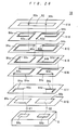
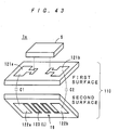
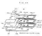
- the power feeding circuit board 10 includes the power feeding circuit 16 of a lumped-constant LC series type having a helical inductance element L and capacitance elements C1 and C2. More specifically, as shown in Fig. 4 , ceramic sheets 11A to 11G made of a dielectric material are laminated, pressed, and sintered so as to form the power feeding circuit board 10.
- the ceramic sheet 11A includes connection electrodes 12 and via-hole conductors 13a formed therein.
- the ceramic sheet 11B includes capacitor electrodes 14a formed therein.
- the ceramic sheet 11C includes capacitor electrodes 14b and via-hole conductors 13b formed therein.
- the ceramic sheet 11D includes via-hole conductors 13c formed therein.
- the ceramic sheet 11E includes conductor patterns 15a and via-hole conductors 13d formed therein.
- the (at least one) ceramic sheet 11F includes via-hole conductors 13e formed therein.
- the ceramic sheet 11G includes conductor patterns 15b formed therein.
- Each of the ceramic sheets 11A to 11G may be made of a magnetic ceramic material.
- the power feeding circuit board 10 can be easily manufactured using a known multilayer fabrication method, such as a sheet lamination method or a thick film printing method.
- the inductance element L and the capacitance elements C1 and C2 are formed.
- the inductance element L follows a helical path about a winding axis which is parallel to the radiating plate 20.
- the capacitor electrodes 14b are connected to either end of the inductance element L.
- each of the capacitor electrodes 14a is connected to one of the connection electrodes 12 via the via-hole conductor 13a.
- the connection electrode 12 that forms an electrode pattern on the board side is DC-connected to an electrode pattern (not shown) of the wireless IC chip 5 on the chip side via a solder bump 6.
- a transmission signal is fed from the inductance element L, which is a coil-shaped electrode pattern in the power feeding circuit 16, to the radiating plate 20 via a magnetic field.
- a reception signal is fed from the radiating plate 20 to the inductance element L via a magnetic field. Accordingly, it is desirable that, among the inductance element L and the capacitance elements C1 and C2 that form a resonance circuit, the inductance element L is disposed so as to be closer to the radiating plate 20.
- the radiating plate 20 is a long rectangular plate made of a nonmagnetic material, such as an aluminum foil or a copper foil. That is, the radiating plate 20 is a both-end-open type metal plate.
- the radiating plate 20 is formed on a flexible insulating resin film 21, such as a PET.
- the lower surface of the power feeding circuit board 10 is bonded to the radiating plate 20 with an insulating adhesive layer composed of an adhesive agent 18 in-between.
- the thickness of the wireless IC chip 5 is in the range of 50 ⁇ m to 100 ⁇ m.
- the thickness of the solder bump 6 is about 20 ⁇ m.
- the thickness of the power feeding circuit board 10 is in the range of 200 ⁇ m to 500 ⁇ m.
- the thickness of the adhesive agent 18 is in the range of 0. 1 ⁇ m to 10 ⁇ m.
- the thickness of the radiating plate 20 is in the range of 1 ⁇ m to 50 ⁇ m.
- the thickness of the film 21 is in the range of 10 ⁇ m to 100 ⁇ m.
- the size (area) of the wireless IC chip 5 can be varied, such as 0.4 mm by 0.4 mm or 0.9 mm by 0.8 mm.
- the size (area) of the power feeding circuit board 10 can be from the same size as the wireless IC chip 5 to about 3 mm by 3 mm.
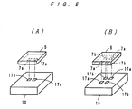
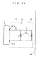
- Fig. 5 illustrates connection arrangements between the wireless IC chip 5 and the power feeding circuit board 10.
- a pair of antenna (balanced) terminals 7a and 17a are provided on the lower surface of the wireless IC chip 5 and the upper surface of the power feeding circuit board 10, respectively.
- Fig. 5B illustrates another connection arrangement.
- ground terminals 7b and 17b are provided on the lower surface of the wireless IC chip 5 and the upper surface of the power feeding circuit board 10, respectively, in addition to the pair of antenna (balanced) terminals 7a and 17a.
- the ground terminal 17b of the power feeding circuit board 10 is terminated and is not connected to any other elements of the power feeding circuit board 10.
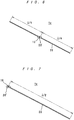
- the radiating plate 20 has a slender shape, and an area 20' of the radiating plate 20 to which the power feeding circuit board 10 is bonded is greater than the board 10. In this way, precise positioning is not required when the power feeding circuit board 10 is bonded to the radiating plate 20a, and stable electrical characteristics can be obtained.
- Fig. 3 illustrates an equivalent circuit of the wireless IC device 1a.
- the wireless IC device 1a receives a high-frequency signal (e.g., a signal in a UHF band) radiated from a reader/writer (not shown) at the radiating plate 20.
- a high-frequency signal e.g., a signal in a UHF band
- the wireless IC device 1a supplies the wireless IC chip 5 with only a reception signal in a predetermined frequency band.
- the wireless IC device 1a extracts predetermined energy from the reception signal, and by using this energy as a driving source, the wireless IC device 1a matches the information stored in the wireless IC chip 5 with a predetermined frequency at the power feeding circuit 16. Thereafter, the wireless IC device 1a propagates a transmission signal from the inductance element L of the power feeding circuit 16 to the radiating plate 20 via magnetic coupling. The radiating plate 20 transmits the transmission signal to the reader/writer.
- the coupling of the power feeding circuit 16 with the radiating plate 20 is mainly achieved via a magnetic field.
- coupling via an electric field may be present (electromagnetic coupling).
- the wireless IC chip 5 is directly DC-connected to the power feeding circuit board 10, which incorporates the power feeding circuit 16.
- the power feeding circuit board 10 has substantially the same area as the wireless IC chip 5, and is rigid. Accordingly, as compared with the existing case where the wireless IC chip 5 is mounted on a flexible film having a large area, the wireless IC chip 5 can be precisely positioned and mounted on the power feeding circuit board 10. Furthermore, the power feeding circuit board 10 is made of a ceramic material and has an excellent resistance to heat, and therefore, the wireless IC chip 5 can be soldered to the power feeding circuit board 10.
- the wireless IC chip 5 can be bonded to the power feeding circuit board 10 without using an expensive ultrasonic bonding method that has been conventionally adopted.
- the cost can be reduced, and there is no danger that the wireless IC chip 5 may be damaged due to pressure applied during ultrasonic bonding.
- a self-alignment effect provided by solder reflow can be used.
- the resonance frequency properties are determined by the resonance circuit including the inductance element L and the capacitance elements C1 and C2.
- the resonance frequency of a signal radiated from the radiating plate 20 is substantially the same as the self-resonance frequency of the power feeding circuit 16.
- the maximum gain of the signal is substantially determined by at least one of the size and shape of the power feeding circuit 16 and the distance and medium between the power feeding circuit 16 and the radiating plate 20. More specifically, according to the first example, the electrical length of the radiating plate 20 is set to 1/2 of the resonance frequency X. However, the electrical length of the radiating plate 20 need not be an integer multiple of ⁇ /2.
- the frequency of a signal radiated from the radiating plate 20 is substantially determined by the resonance frequency of the resonance circuit (the power feeding circuit 16). Therefore, the frequency characteristics are not substantially dependent on the electrical length of the radiating plate 20. It is desirable that the electrical length of the radiating plate 20 is an integer multiple of ⁇ /2 so as to maximize the gain.
- the resonance frequency characteristics of the power feeding circuit 16 are determined by the resonance circuit composed of the inductance element L and the capacitance elements C1 and C2 incorporated in the power feeding circuit board 10. Accordingly, even when the wireless IC device 1a is inserted into a book, the resonance frequency characteristics do not change. In addition, even when the wireless IC device 1a is curled to change the shape or the size of the radiating plate 20, the resonance frequency characteristics do not change. Furthermore, since the coil-shaped electrode pattern that forms the inductance element L is disposed so that the winding axis thereof is parallel to the radiating plate 20, the center frequency does not advantageously vary. Still furthermore, since the capacitance elements C1 and C2 are disposed downstream of the wireless IC chip 5, a low-frequency surge is prevented by the capacitance elements C1 and C2. Thus, the wireless IC chip 5 can be protected from a surge.
- the power feeding circuit board 10 is a rigid multilayer board, the wireless IC chip 5 can be easily soldered.
- the radiating plate 20 is formed from a flexible metal film supported by the flexible film 21. Therefore, the radiating plate 20 can be easily bonded to, for example, a cylindrical member, such as a PET bottle or a soft bag made of a plastic film.
- the resonance circuit may function as a matching circuit for matching the impedance of the wireless IC chip with the impedance of the radiating plate.
- the power feeding circuit board may further include a matching circuit that includes an inductance element and a capacitance element and that is provided separately from the resonance circuit.
- the resonance circuit includes the function of a matching circuit, the design of the resonance circuit is complicated.
- the resonance circuit and the matching circuit can be designed independently.
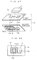
- the radiating plate 20 branches into two parts at an angle of 90°. That is, the radiating plate 20 includes a radiating section 20a that extends in an x-axis direction and a radiating section 20b that extends in a y-axis direction in an x-y plane. Further, the radiating plate 20 has an extension of the radiating section 20a, which serves as a power feeding section 20d. On the power feeding section 20d, a power feeding circuit board 10 having a wireless IC chip 5 mounted thereon is bonded.
- the internal structure of the power feeding circuit board 10 is similar to that of the first example.
- the operation and advantages of the second example are the same as those of the first example.
- the radiating sections 20a and 20b extend in the x-axis direction and the y-axis direction, respectively, the radiating plate 20 can receive circularly polarized waves. Accordingly, the antenna gain is improved.
- a radiating plate 20 in a wireless IC device 1c, includes radiating sections 20a, 20b, and 20c that extend in an x-axis direction, a y-axis direction, and a z-axis direction, respectively, in an x-y-z space.
- a power feeding circuit board 10 having a wireless IC chip 5 mounted thereon is bonded onto a power feeding section 20d which is an extension of the radiating section 20a.
- the wireless IC device 1c can be mounted at a corner of a box-shaped article. Since the radiating sections 20a, 20b, and 20c are disposed three-dimensionally, the directivity of the antenna can be eliminated. Thus, in any direction, efficient transmission and reception can be performed. In addition, the operation and advantages of the wireless IC device 1c are the same as those of the first example.
- the radiating plate 20 having a large area and made of an aluminum foil is formed on an insulating flexible plastic film 21 having a large area.
- a power feeding circuit board 10 having a wireless IC chip 5 mounted thereon is bonded to the radiating plate 20 at any location.
- the other structure of the wireless IC device 1d that is, the internal structure of the power feeding circuit board 10 is similar to that of the first example. Accordingly, the operation and advantages of the fourth example are the same as those of the first example. In addition, the fourth example has an advantage in that high-precision positioning is not required when the power feeding circuit board 10 is bonded to the radiating plate 20.
- the radiating plate 20 having a large area and made of an aluminum foil is formed in a mesh.
- the entire radiating plate 20 may be a mesh, or alternatively, a part of the radiating plate 20 may be a mesh.
- the other structures of the wireless IC device 1e are similar to those of the fourth example. Accordingly, high-precision positioning is not required when the power feeding circuit board 10 is bonded to the radiating plate 20. In addition, since the magnetic flux of the coil-shaped electrode pattern passes through the openings of the mesh, a change (a decrease) in magnetic flux emanating from the power feeding circuit board 10 is reduced. Thus, more magnetic fluxes can pass through the radiating plate 20, and the propagation efficiency of signal energy is improved. In addition, a shift of the frequency caused by bonding can be reduced.
- an adhesive agent 18 is applied to the entire surface of the film 21 to which the power feeding circuit board 10 is bonded via the radiating plate 20.
- the adhesive agent 18 enables the wireless IC device If to be bonded to an arbitrary portion of an article.
- the other structure of the wireless IC device If, that is, the internal structure of the power feeding circuit board 10 is similar to that of the first example. Accordingly, the operation and advantages of the sixth example are the same as those of the first example.
- a wireless IC device 1g has a power feeding circuit board 10 incorporating an inductance element L that serves as the power feeding circuit 16 and that has a coil-shaped electrode pattern.
- a capacitance element C that forms an LC parallel resonance circuit is provided in the form of a floating capacitance (distributed-constant-type capacitance) between the conductor patterns of the inductance element L.
- the coil-shaped electrode pattern when even one coil-shaped electrode pattern has self-resonance, the coil-shaped electrode pattern can function as an LC parallel resonance circuit by using the L component of the coil-shaped electrode pattern itself and the C component generated as a line floating capacitance, and a power feeding circuit 16 can be achieved. Accordingly, the wireless IC device 1g receives a high-frequency signal (e.g., a signal in a UHF band) radiated from a reader/writer (not shown) at the radiating plate 20.
- a high-frequency signal e.g., a signal in a UHF band
- the wireless IC device 1g By resonating the power feeding circuit 16 (the LC parallel resonance circuit composed of the inductance element L and the capacitance element C) that is mainly magnetically coupled with the radiating plate 20, the wireless IC device 1g supplies the wireless IC chip 5 with only a reception signal in a predetermined frequency band. Meanwhile, the wireless IC device 1g extracts predetermined energy from the reception signal, and by using this energy as a driving source, the wireless IC device 1g matches the information stored in the wireless IC chip 5 with a predetermined frequency at the power feeding circuit 16. Thereafter, the wireless IC device 1g propagates a transmission signal from the inductance element L of the power feeding circuit 16 to the radiating plate 20 via magnetic coupling. The radiating plate 20 transmits the transmission signal to the reader/writer.
- a wireless IC device 1h includes a dipole-type power feeding circuit 16 and radiating plates 20.
- the power feeding circuit 16 includes two LC parallel resonance circuits disposed in a power feeding circuit board.
- An inductance element L1 and a capacitance element C1 are connected to a first port side of the wireless IC chip 5.
- An inductance element L2 and a capacitance element C2 are connected to a second port side of the wireless IC chip 5.
- the inductance element L1 and the capacitance element C1 face one of the radiating plates 20.
- the inductance element L2 and the capacitance element C2 face the other radiating plate 20.
- An end of the inductance element L1 and the capacitance element C1 is open. Note that the first port and the second port form the I/O ports of a differential circuit.
- the wireless IC device 1h receives a high-frequency signal (e.g., a signal in a UHF band) radiated from a reader/writer (not shown) at the radiating plates 20.
- a high-frequency signal e.g., a signal in a UHF band
- the wireless IC device 1h supplies the wireless IC chip 5 with only a reception signal in a predetermined frequency band.
- the wireless IC device 1h extracts predetermined energy from the reception signal, and by using this energy as a driving source, the wireless IC device 1h matches the information stored in the wireless IC chip 5 with a predetermined frequency at the power feeding circuit 16. Thereafter, the wireless IC device 1h propagates a transmission signal from the inductance elements L1 and L2 of the power feeding circuit 16 to the radiating plates 20 via magnetic coupling. The radiating plates 20 transmit the transmission signal to the reader/writer.
- a wireless IC device 1i includes a dipole-type power feeding circuit 16 and radiating plates 20.
- the power feeding circuit 16 includes two LC series resonance circuits disposed in a power feeding circuit board.
- An inductance element L1 faces one of the radiating plates 20, and an inductance element L2 faces the other radiating plate 20.
- Capacitance elements C1 and C2 are grounded.
- the wireless IC device 1i receives a high-frequency signal (e.g., a signal in a UHF band) radiated from a reader/writer (not shown) at the radiating plates 20.
- a high-frequency signal e.g., a signal in a UHF band
- the wireless IC device 1i supplies the wireless IC chip 5 with only a reception signal in a predetermined frequency band.
- the wireless IC device 1i extracts predetermined energy from the reception signal, and by using this energy as a driving source, the wireless IC device 1i matches the information stored in the wireless IC chip 5 with a predetermined frequency at the power feeding circuit 16. Thereafter, the wireless IC device 1i propagates a transmission signal from the inductance elements L1 and L2 of the power feeding circuit 16 to the radiating plates 20 via magnetic coup ng. The radiating plates 20 transmit the transmission signal to the reader/writer.
- a wireless IC device 1j is of a monopole type.
- a power feeding circuit 16 includes an LC series resonance circuit, which is composed of an inductance element L and a capacitance element C, incorporated in a power feeding circuit board 10.
- a coil-shaped electrode pattern that forms the inductance element L has a winding axis that is perpendicular to the radiating plate 20.
- the power feeding circuit 16 is mainly magnetically coupled with the radiating plate 20.
- ceramic sheets 31A to 31F made of a dielectric material are laminated, pressed, and sintered so as to form the power feeding circuit board 10.
- the ceramic sheet 31A includes connection electrodes 32 and via-hole conductors 33a formed therein.
- the ceramic sheet 31B includes a capacitor electrode 34a and a via-hole conductor 33b formed therein.
- the ceramic sheet 31C includes a capacitor electrode 34b, a via-hole conductor 33c, and the via-hole conductor 33b formed therein.
- the (at least one) ceramic sheet 31D includes a conductor pattern 35a, a via-hole conductor 33d, and the via-hole conductor 33b formed therein.
- the (at least one) ceramic sheet 31E includes a conductor pattern 35b, a via-hole conductor 33e, and the via-hole conductor 33b formed therein.
- the ceramic sheet 31F includes a conductor pattern 35c formed therein.
- the power feeding circuit 16 including the LC series resonance circuit can be obtained.
- the capacitance element C is connected in series to the inductance element L having a helical winding axis which is parallel to the radiating plate 20.
- the capacitor electrode 34a is connected to one of the connection electrodes 32 via the via-hole conductor 33a.
- the capacitor electrode 34a is connected to the wireless IC chip 5 via a solder bump 6.
- One end of the inductance element L is connected to the other connection electrode 32 via the via-hole conductor 33b and is further connected to the wireless IC chip 5 via a solder bump 6.
- the wireless IC device 1j receives a high-frequency signal (e.g., a signal in a UHF band) radiated from a reader/writer (not shown) at the radiating plate 20.
- a high-frequency signal e.g., a signal in a UHF band
- the wireless IC device 1j supplies the wireless IC chip 5 with only a reception signal in a predetermined frequency band.
- the wireless IC device 1j extracts predetermined energy from the reception signal, and by using this energy as a driving source, the wireless IC device 1j matches the information stored in the wireless IC chip 5 with a predetermined frequency at the power feeding circuit 16. Thereafter, the wireless IC device 1j propagates a transmission signal from the inductance element L of the power feeding circuit 16 to the radiating plate 20 via magnetic coupling. The radiating plate 20 transmits the transmission signal to the reader/writer.
- the coil-shaped electrode pattern since the coil-shaped electrode pattern has a winding axis perpendicular to the radiating plate 20, the magnetic flux component arriving at the radiating plate 20 increases. Therefore, the propagation efficiency of signal energy improves, and the gain increases.
- the winding width (coil diameter) of the coil-shaped electrode pattern of the inductance element L described in the tenth example gradually increases towards the radiating plate 20.
- the other structure is similar to that of the tenth example.
- the operation and advantages of the eleventh example are similar to those of the tenth example.
- the winding width (coil diameter) of the coil-shaped electrode pattern of the inductance element L gradually increases towards the radiating plate 20, the propagation efficiency of signal energy is improved.
- a wireless IC device 11 is of a dipole type.
- the wireless IC device 11 includes a power feeding circuit 16 composed of two LC series resonance circuits disposed in a power feeding circuit board 10.
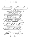
- ceramic sheets 41A to 41F made of a dielectric material are laminated, pressed, and sintered so as to form the power feeding circuit board 10.
- the ceramic sheet 41A includes connection electrodes 42 and via-hole conductors 43a formed therein.
- the ceramic sheet 41B includes capacitor electrodes 44a formed therein.
- the ceramic sheet 41C includes capacitor electrodes 44b and via-hole conductors 43b formed therein.
- the (at least one) ceramic sheet 41D includes conductor patterns 45a and via-hole conductors 43c formed therein.
- the (at least one) ceramic sheet 41E includes conductor patterns 45b and via-hole conductors 43d formed therein.
- the ceramic sheet 41F includes conductor patterns 45c formed therein.
- the power feeding circuit 16 including the LC series resonance circuit can be obtained.
- capacitance elements C1 and C2 are connected in series to inductance elements L1 and L2 having helical winding axes which are perpendicular to the radiating plate 20, respectively.
- the capacitor electrodes 44a are connected to the connection electrodes 42 via the via-hole conductors 43a.
- the capacitor electrodes 44a are connected to the wireless IC chip 5 via solder bumps 6.
- the wireless IC device 11 receives a high-frequency signal (e.g., a signal in a UHF band) radiated from a reader/writer (not shown) at the radiating plates 20.
- a high-frequency signal e.g., a signal in a UHF band
- the wireless IC device 11 supplies the wireless IC chip 5 with only a reception signal in a predetermined frequency band.
- the wireless IC device 11 extracts predetermined energy from the reception signal, and by using this energy as a driving source, the wireless IC device 11 matches the information stored in the wireless IC chip 5 with a predetermined frequency at the power feeding circuit 16. Thereafter, the wireless IC device 11 propagates a transmission signal from the inductance elements L1 and L2 of the power feeding circuit 16 to the radiating plates 20 via magnetic coupling. The radiating plates 20 transmit the transmission signal to the reader/writer.
- the capacitance elements C1 and C2 are disposed downstream of the wireless IC chip 5.
- the capacitance element C1 is disposed between the wireless IC chip 5 and the inductance element L1
- the capacitance element C2 is disposed between the wireless IC chip 5 and the inductance element L2. Accordingly, surge resistance is improved. Since surge is a low-frequency electrical current up to 200 MHz, the surge can be removed by the capacitance elements C1 and C2. Thus, surge breakdown of the wireless IC chip 5 is prevented.
- the resonance circuit composed of the capacitance element C1 and the inductance element L1 is not coupled to the resonance circuit composed of the capacitance element C2 and the inductance element L2.
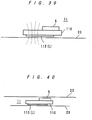
- a power feeding circuit 56 including a coil-shaped electrode pattern, that is, a spiral inductance element is formed on the surface of a power feeding circuit board 50, which is a rigid single-layer board made of ceramic or a heat-resisting resin. Either end of the power feeding circuit 56 is directly connected to a wireless IC chip 5 via a solder bump.
- the power feeding circuit board 50 is bonded to a film 21 that holds a radiating plate 20 by an adhesive agent.
- a conductor pattern 56a is separated from conductor patterns 56b and 56c, which cross the conductor pattern 56a, by an insulating film (not shown).
- the power feeding circuit 56 forms an LC parallel resonance circuit wherein a floating capacitance formed between the spirally wound conductor patterns is used as a capacitance component.
- the power feeding circuit board 50 is a single-layer board made of a dielectric material or a magnetic material.
- the power feeding circuit 56 is mainly magnetically coupled with the radiating plate 20. Accordingly, like the above-described examples, the wireless IC device 1m receives a high-frequency signal (e.g. , a signal in a UHF band) radiated from a reader/writer (not shown) at the radiating plate 20. By resonating the power feeding circuit 56, the wireless IC device 1m supplies the wireless IC chip 5 with only a reception signal in a predetermined frequency band.
- a high-frequency signal e.g. , a signal in a UHF band
- the wireless IC device 1m extracts predetermined energy from the reception signal, and by using this energy as a driving source, the wireless IC device 1m matches the information stored in the wireless IC chip 5 with a predetermined frequency at the power feeding circuit 56. Thereafter, the wireless IC device 1 m propagates a transmission signal from the inductance element of the power feeding circuit 56 to the radiating plate 20 via magnetic coupling. The radiating plate 20 transmits the transmission signal to the reader/writer.
- the wireless IC chip 5 is mounted on the rigid power feeding circuit board 50 having a small area. Accordingly, the wireless IC chip 5 can be precisely positioned and can be connected to the power feeding circuit board 50 using a solder bump.
- a power feeding circuit 56 includes a coil-shaped electrode pattern incorporated in a power feeding circuit board 50.
- ceramic sheets 51A to 51D made of a dielectric material are laminated, pressed, and sintered so as to form the power feeding circuit board 50.
- the ceramic sheet 51A includes connection electrodes 52 and via-hole conductors 53a formed therein.
- the ceramic sheet 51B includes a conductor pattern 54a and via-hole conductors 53b and 53c formed therein.
- the ceramic sheet 51C includes a conductor pattern 54b formed therein.
- Each of a plurality of the ceramic sheets 51D has no components therein.
- the power feeding circuit board 50 incorporating the power feeding circuit 56 can be obtained.
- the power feeding circuit 56 includes a resonance circuit composed of a spirally wound inductance element and a capacitance element defined by a floating capacitance between lines of the spirally wound electrode pattern.
- the connection electrodes 52 disposed at either end of the power feeding circuit 56 are connected to the wireless IC chip 5 via solder bumps 6.
- the operation and advantages of the fourteenth example are the same as those of the thirteenth example.
- a wireless IC device 10 includes a wireless IC chip 5 and a power feeding circuit board 10 that are capacitively coupled with each other, and the power feeding circuit board 10 is DC-connected to a radiating plate 20.
- the power feeding circuit board 10 incorporates a power feeding circuit 16 including two LC series resonance circuits.
- the winding axes of inductance elements L1 and L2 are perpendicular to the radiating plate 20.
- One end of the inductance element L1 and one end of the inductance element L2 are connected to capacitor electrodes 65a and 65b that form capacitance elements C1 and C2 (refer to Fig. 26 ), respectively.
- connection electrode 62 disposed on the upper surface (in Figs. 25 and 26 ) of the board 10.
- capacitor electrodes 66a and 66b that form the capacitance elements C1 and C2 are disposed on the upper surface (in Figs. 25 and 26 ) of the wireless IC chip 5.
- ceramic sheets 61A to 61G made of a dielectric material are laminated, pressed, and sintered so as to form the power feeding circuit board 10.
- the sheet 61A includes the connection electrode 62 and via-hole conductors 63a and 63b formed therein.
- Each of the sheets 61B to 61F includes conductor patterns 64a and 64b and via-hole conductors 63c and 63d formed therein.
- the sheet 61G includes capacitor electrodes 65a and 65b formed therein.
- the power feeding circuit 16 including two LC series resonance circuits can be obtained.
- the capacitance elements C1 and C2 are connected in series to the inductance elements L1 and L2, respectively.
- the capacitance element C1 is formed between the two parallel flat electrode patterns, that is, between the electrode 66a serving as a chip-side electrode pattern and the electrode 65a serving as a board-side electrode pattern.
- the capacitance element C2 is formed between the two parallel flat electrode patterns, that is, between the electrode 66b serving as a chip-side electrode pattern and the electrode 65b serving as a board-side electrode pattern.
- the wireless IC chip 5 is bonded and connected to the power feeding circuit board 10 via an insulating adhesive layer.
- the power feeding circuit board 10 is also DC-connected to the radiating plate 20 via a connection electrode 62 which is a second board-side electrode pattern.
- the connection electrode 62 and the radiating plate 20 may be connected to each other via a solder, a conductive adhesive agent or the like.
- the wireless IC device 1o receives a high-frequency signal (e.g., a signal in a UHF band) radiated from a reader/writer (not shown) at the radiating plate 20.
- a high-frequency signal e.g., a signal in a UHF band
- the wireless IC device 1o supplies the wireless IC chip 5 with only a reception signal in a predetermined frequency band.
- the wireless IC device 1o extracts predetermined energy from the reception signal, and by using this energy as a driving source, the wireless IC device 1o matches the information stored in the wireless IC chip 5 with a predetermined frequency at the power feeding circuit 16. Thereafter, the wireless IC device 1o propagates a transmission signal to the radiating plate 20 that is DC-connected to the power feeding circuit 16. The radiating plate 20 transmits the transmission signal to the reader/writer.
- the power feeding circuit 16 is capacitively coupled with the wireless IC chip 5 by the capacitance elements C1 and C2, so that electric power and transmission/reception signals are exchanged therebetween.
- the areas of the capacitor electrodes 65a and 65b formed on the power feeding circuit board 10 are larger than the areas of the capacitor electrodes 66a and 66b formed on the wireless IC chip 5, respectively. Accordingly, even when the accuracy in positioning of the wireless IC chip 5 on the power feeding circuit board 10 somewhat varies, variations in capacitance formed between the capacitor electrodes 65a and 66a and between the capacitor electrodes 65b and 66b are reduced. In addition, the capacitance elements C1 and C2 are disposed downstream of the wireless IC chip 5, which improves the resistance to surge.
- a power feeding circuit board 10 is capacitively coupled with radiating plates 20.
- the power feeding circuit board 10 incorporates a power feeding circuit 16 including two LC series resonance circuits.
- One end of an inductance element L1 and one end of an inductance element L2 are connected to the wireless IC chip 5.
- the other end of the inductance element L1 and the other end of the inductance element L2 are connected to capacitor electrodes 72a and 72b that are disposed on the upper surface (in Figs. 27 and 28 ) of the board 10 and that form capacitance elements C1 and C2 (refer to Fig. 28 ), respectively.
- An end portion 20a of one of the radiating plates 20 serves as the other capacitor electrode for the capacitance element C1, while an end portion 20b of the other radiating plate 20 serves as the other capacitor electrode for the capacitance element C2.
- ceramic sheets 71A to 71F made of a dielectric material are laminated, pressed, and sintered so as to form the power feeding circuit board 10.
- the sheet 71A includes the capacitor electrodes 72a and 72b and via-hole conductors 73a and 73b formed therein.
- Each of the sheets 71B to 71E includes conductor patterns 74a and 74b and via-hole conductors 73c and 73d formed therein.
- the sheet 71F includes the conductor patterns 74a and 74b formed on one surface and connection electrodes 75a and 75b formed on the other surface thereof.
- the conductor patterns 74a and 74b of the sheet 71F are connected to the connection electrodes 75a and 75b through via-hole conductors 73e and 73f, respectively.
- the power feeding circuit 16 including two LC series resonance circuits can be obtained.
- the capacitance elements C1 and C2 are connected in series to the inductance elements L1 and L2, respectively.
- the capacitor electrodes 72a and 72b which are flat electrode patterns parallel to the radiating plates 20 face the end portions 20a and 20b of the radiating plates 20, respectively, with the insulating adhesive agent in-between, and thus, the capacitance elements C1 and C2 are defined.
- connection electrodes 75a and 75b are connected to the wireless IC chip 5 via solder bumps, one end of the inductance element L1 and one end of the inductance element L2 are connected to the wireless IC chip 5, and therefore, the power feeding circuit board 10 is DC-connected to the wireless IC chip 5.
- the adhesive agent layer has a dielectric property, and the capacitance of the capacitance elements C1 and C2 is increased.
- the capacitor electrodes 72a and 72b serving as a second board-side electrode patterns are disposed on the upper surface (in Figs. 27 and 28 ) of the power feeding circuit board 10
- the capacitor electrodes 72a and 72b may be formed inside the power feeding circuit board 10 (but at a location adjacent to the radiating plates 20).
- the capacitor electrodes 72a and 72b may be formed in an inner layer of the board 10.
- the wireless IC device 1p receives a high-frequency signal (e.g., a signal in a UHF band) radiated from a reader/writer (not shown) at the radiating plate 20.
- a high-frequency signal e.g., a signal in a UHF band
- the wireless IC device 1p supplies the wireless IC chip 5 with only a reception signal in a predetermined frequency band.
- the wireless IC device 1p extracts predetermined energy from the reception signal, and by using this energy as a driving source, the wireless IC device 1p matches the information stored in the wireless IC chip 5 with a predetermined frequency at the power feeding circuit 16. Thereafter, the wireless IC device 1p propagates a transmission signal to the radiating plate 20 via the capacitive coupling provided by the capacitance elements C1 and C2. The radiating plate 20 transmits the transmission signal to the reader/writer.
- a wireless IC device 1q includes a power feeding circuit 16 including inductance elements L1 and L2 that are magnetically coupled with each other.
- the inductance element L1 is connected to a wireless IC chip 5 via capacitance elements C1a and C1b.
- the inductance element L1 is connected to the inductance element L2 in parallel via capacitance elements C2a and C2b. That is, the power feeding circuit 16 includes an LC series resonance circuit composed of the inductance element L1 and the capacitance elements C1a and C1b.
- the power feeding circuit 16 further includes an LC series resonance circuit composed of the inductance element L2 and the capacitance elements C2a and C2b.
- the two resonance circuits are coupled with each other via magnetic coupling indicated by "M” shown in Fig. 29 .
- the two inductance elements L1 and L2 are magnetically coupled with the radiating plate 20.
- ceramic sheets 81A to 81H made of a dielectric material are laminated, pressed, and sintered so as to form the power feeding circuit board 10.
- the sheet 81A has no components formed therein.
- the sheet 81B includes conductor patterns 82a and 82b and via-hole conductors 83a, 83b, 84a, and 84b formed therein.
- the sheet 81C includes conductor patterns 82a and 82b and via-hole conductors 83c, 84c, 83e, and 34e formed therein.
- the sheet 81D includes the conductor patterns 82a and 82b and via-hole conductors 83d, 84d, 83e, and 34e formed therein.
- the sheet 81E includes capacitor electrodes 85a and 85b and a via-hole conductor 83e formed therein.
- the sheet 81F includes capacitor electrodes 86a and 86b formed therein.
- the sheet 81G has no components formed therein.
- the sheet 81H includes capacitor electrodes 87a and 87b formed on the bottom surface (in Fig. 30 ) thereof.
- the conductor patterns 82a are connected to each other via the-via-hole conductors 83b and 83c so as to form the inductance element L1. Also, the conductor patterns 82b are connected to each other via the via-hole conductors 84b and 84c so as to form the inductance element L2.
- the capacitor electrodes 86a and 87a form the capacitance element C1a.
- the capacitor electrode 86a is connected to one end of the inductance element L1 via the via-hole conductor 83e.
- the capacitor electrodes 86b and 87b form the capacitance element C1b.
- the capacitor electrode 86b is connected to the other end of the inductance element L1 via the via-hole conductor 83d. Also, the capacitor electrodes 85a and 86a form the capacitance element C2a. The capacitor electrode 85a is connected to one end of the inductance element L2 via the via-hole conductor 84e. The capacitor electrodes 85b and 86b form the capacitance element C2b. The capacitor electrode 85b is connected to the other end of the inductance element L2 via the via-hole conductor 84d.
- the wireless IC device 1q receives a high-frequency signal (e.g., a signal in a UHF band) radiated from a reader/writer (not shown) at the radiating plate 20.
- a high-frequency signal e.g., a signal in a UHF band
- the wireless IC device 1q supplies the wireless IC chip 5 with only a reception signal in a predetermined frequency band.
- the wireless IC device 1q extracts predetermined energy from the reception signal, and by using this energy as a driving source, the wireless IC device 1q matches the information stored in the wireless IC chip 5 with a predetermined frequency at the power feeding circuit 16. Thereafter, the wireless IC device 1q propagates a transmission signal from the inductance elements L1 and L2 of the power feeding circuit 16 to the radiating plate 20 via magnetic coupling. The radiating plate 20 transmits the transmission signal to the reader/writer.
- the bandwidth X wherein a reflection characteristic of -5 dB or less can be obtained is an extremely broad frequency band not less than about 150 MHz.
- the power feeding circuit 16 includes a plurality of LC resonance circuits having the inductance elements L1 and L2 that are magnetically coupled with each other with high degree of coupling.
- the capacitance elements C1a and C1b are disposed downstream of the wireless IC chip 5, which improves the resistance to surge.
- a wireless IC device 1r includes a power feeding circuit 16 having inductance elements L1 and L2 that are magnetically coupled with each other with high degree of coupling.
- the inductance element L1 is magnetically coupled with an inductance element L5 provided in the wireless IC chip 5.
- the inductance element L2 and a capacitance element C2 form an LC series resonance circuit.
- the capacitance element C1 is capacitively coupled with the radiating plate 20.
- a capacitance element C3 is inserted between the capacitance elements C1 and C2.
- ceramic sheets 91A to 91E made of a dielectric material are laminated, pressed, and sintered so as to form the power feeding circuit board 10.
- the sheet 91A includes conductor patterns 92a and 92b and via-hole conductors 93a, 93b, 94a, and 94b formed therein.
- the sheet 91B includes a capacitor electrode 95 and via-hole conductors 93c, 93d, and 94c formed therein.
- the sheet 91C includes a capacitor electrode 96 and the via-hole conductors 93c and 93d formed therein.
- the sheet 91D includes a capacitor electrode 97 and the via-hole conductor 93c formed therein.
- the sheet 91E includes a capacitor electrode 98.
- the conductor pattern 92a forms the inductance element L1.
- the conductor pattern 92b forms the inductance element L2.
- the capacitor electrodes 97 and 98 form the capacitance element C1.
- One end of the inductance element L1 is connected to the capacitor electrode 98 via the via-hole conductors 93a and 93c.
- the other end of the inductance element L1 is connected to the capacitor electrode 97 via the via-hole conductors 93b and 93d.
- the capacitor electrodes 95 and 96 form the capacitance element C2.
- One end of the inductance element L2 is connected to the capacitor electrode 96 via the via-hole conductors 94a and 94c.
- the other end of the inductance element L2 is connected to the capacitor electrode 95 via the via-hole conductor 94b.
- the capacitor electrodes 96 and 97 form the capacitance element C3.
- a coil-shaped electrode pattern 99 is disposed on a surface of the wireless IC chip 5 as a chip-side electrode pattern, and the coil-shaped electrode pattern 99 defines the inductance element L5.
- a protecting film for example, a resin film is provided on the surface of the coil-shaped electrode pattern 99.
- the inductance elements L1 defined by the coil-shaped electrode pattern serving as a board-side electrode pattern is magnetically coupled with the coil-shaped electrode pattern 99.
- the wireless IC device 1r receives a high-frequency signal (e.g., a signal in a UHF band) radiated from a reader/writer (not shown) at the radiating plate 20.
- a high-frequency signal e.g., a signal in a UHF band
- the wireless IC device 1r supplies the wireless IC chip 5 with only a reception signal in a predetermined frequency band.
- the wireless IC device 1r extracts predetermined energy from the reception signal, and by using this energy as a driving source, the wireless IC device 1r matches the information stored in the wireless IC chip 5 with a predetermined frequency at the power feeding circuit 16. Thereafter, the wireless IC device 1r propagates a transmission signal from the inductance elements L1 and L2 of the power feeding circuit 16 to the radiating plate 20 via magnetic coupling. The radiating plate 20 transmits the transmission signal to the reader/writer.
- the power feeding circuit 16 is magnetically coupled with the wireless IC chip 5 by the inductance elements L1 and L5. Thus, electrical power and transmission/reception signals are exchanged.
- a wireless IC device Is includes a power feeding circuit 16 having inductance elements L1, L2, and L3 that are magnetically coupled with each other with high degree of coupling.
- the inductance element L1 is magnetically coupled with an inductance element L5 provided in the wireless IC chip 5.
- the inductance element L2 and capacitance elements C1a and C1b form an LC series resonance circuit.
- the inductance element L3 and capacitance elements C2a and C2b form an LC series resonance circuit.
- the inductance elements L1, L2, and L3 are magnetically coupled with the radiating plate 20.
- ceramic sheets 101A to 101E made of a dielectric material are laminated, pressed, and sintered so as to form the power feeding circuit board 10.
- the sheet 101A includes conductor pattern 102a and via-hole conductors 103a and 103b formed therein.
- the sheet 101B includes capacitor electrodes 104a and 104b formed therein.
- the sheet 101C includes capacitor electrodes 105a and 105b and via-hole conductors 103c and 103d formed therein.
- the sheet 101D includes capacitor electrodes 106a and 106b, the via -ole conductors 103c and 103d, and via-hole conductors 103e and 103f formed therein.
- the sheet 101E includes conductor patterns 102b and 102c formed therein. That is, a space is formed between the electrodes 104a, 105a and 106a and the electrodes 104b, 105b and 106b, which define the capacitance elements, so that the magnetic fluxes emanated from the inductance element L1 reach the inductance elements L2, L3, and the radiating plate 20.
- the conductor pattern 102a forms the inductance element L1.
- the conductor pattern 102b forms the inductance element L2.
- the conductor pattern 102c forms the inductance element L3.
- the capacitor electrodes 104a and 105a form the capacitance element C1a.
- the capacitor electrodes 104b and 105b form the capacitance element C1b.
- the capacitor electrodes 105a and 106a form the capacitance element C2a.
- the capacitor electrodes 105b and 106b form the capacitance element C2b.
- One end of the inductance element L1 is connected to the capacitor electrode 104a via the via-hole conductor 103a.
- the other end of the inductance element L1 is connected to the capacitor electrode 104b via the via-hole conductor 103b.
- One end of the inductance element L2 is connected to the capacitor electrode 105a via the via-hole conductor 103c.
- the other end of the inductance element L2 is connected to the capacitor electrode 106b via the via-hole conductor 103f.
- One end of the inductance element L3 is connected to the capacitor electrode 106a via the via-hole conductor 103e.
- the other end of the inductance element L3 is connected to the capacitor electrode 105b via the via-hole conductor 103d.
- a coil-shaped electrode pattern 99 as shown in Fig. 34 is disposed on a surface of the wireless IC chip 5 as a chip-side electrode pattern, and the coil-shaped electrode pattern 99 defines the inductance element L5.
- a protecting film for example, a resin film is provided on the surface of the coil-shaped electrode pattern 99.
- the inductance element L1 defined by the coil-shaped electrode pattern serving as a board-side electrode pattern is magnetically coupled with the coil-shaped electrode pattern 99.
- the wireless IC device Is receives a high-frequency signal (e.g., a signal in a UHF band) radiated from a reader/writer (not shown) using the radiating plate 20.
- a high-frequency signal e.g., a signal in a UHF band
- the wireless 1C device Is supplies the wireless IC chip 5 with only a reception signal in a predetermined frequency band.
- the wireless IC device Is extracts predetermined energy from the reception signal, and by using this energy as a driving source, the wireless IC device 1s matches the information stored in the wireless IC chip 5 with a predetermined frequency at the power feeding circuit 16. Thereafter, the wireless IC device Is propagates a transmission signal from the inductance elements L1, L2, and L3 of the power feeding circuit 16 to the radiating plate 20 via magnetic coupling. The radiating plate 20 transmits the transmission signal to the reader/writer.
- the power feeding circuit 16 is magnetically coupled with the wireless IC chip 5 by the inductance elements L1 and L5, and thus, electrical power and transmission/reception signals are exchanged.
- the power feeding circuit 16 includes a plurality of LC resonance circuits having the inductance elements L2 and L3 that are magnetically coupled with each other. Therefore, like the seventeenth example, the frequency band is increased.
- a wireless IC device 1t includes a power feeding circuit board 110 of a single-layer type.
- the equivalent circuit of the wireless IC device It is similar to that shown in Fig. 3 . That is, the power feeding circuit 16 includes an LC series resonance circuit in which capacitance elements C1 and C2 are connected to either end of an inductance element L.
- the power feeding circuit board 110 is a ceramic board made of a dielectric material. As shown in Fig. 37 , capacitor electrodes 111a and 111b are formed on the first surface of the power feeding circuit board 110. Capacitor electrodes 112a and 112b and a conductor pattern 113 are formed on the second surface of the power feeding circuit board 110.
- the capacitor electrodes 111a and 112a form the capacitance element C1.
- the capacitor electrodes 111b and 112b form the capacitance element C2.
- the wireless IC device It receives a high-frequency signal (e.g., a signal in a UHF band) radiated from a reader/writer (not shown) at the radiating plate 20.
- a high-frequency signal e.g., a signal in a UHF band
- the wireless IC device It supplies the wireless IC chip 5 with only a reception signal in a predetermined frequency band.
- the wireless IC device 1t extracts predetermined energy from the reception signal, and by using this energy as a driving source, the wireless IC device 1t matches the information stored in the wireless IC chip 5 with a predetermined frequency at the power feeding circuit 16. Thereafter, the wireless IC device It propagates a transmission signal from the inductance element L of the power feeding circuit 16 to the radiating plate 20 via magnetic coupling. The radiating plate 20 transmits the transmission signal to the reader/writer.
- the inductance element L overlaps the wireless IC chip 5 only partially in a plan view. Accordingly, most magnetic fluxes generated by the inductance element L are not blocked by the wireless IC chip 5. Thus, the magnetic fluxes rise markedly.
- the power feeding circuit board 110 having the wireless IC chip 5 mounted thereon may be sandwiched by radiating plates 20. In this way, the magnetic coupling efficiency between the power feeding circuit 16 and the radiating plates 20 is improved, and gain is also improved.
- the radiating plates 20 may be disposed in a line in the x-axis direction as shown in Fig. 41 , and alternatively, may be disposed in the x-axis direction and in the y-axis direction, respectively, as shown in Fig. 42 .
- a wireless IC device 1u includes an inductance element L formed from a meandering-shaped electrode pattern.
- the equivalent circuit of the wireless IC device 1u is similar to that shown in Fig. 3 . That is, the power feeding circuit 16 includes an LC series resonance circuit in which capacitance elements C1 and C2 are connected to either end of an inductance element L.
- a power feeding circuit board 110 is a ceramic single-layer board made of a dielectric material. As shown in Fig. 43 , capacitor electrodes 121a and 121b are formed on the first surface of the power feeding circuit board 110. Capacitor electrodes 122a and 122b and a meandering conductor pattern 123 are formed on the second surface of the power feeding circuit board 110. The capacitor electrodes 121a and 122a form the capacitance element C1. The capacitor electrodes 121b and 122b form the capacitance element C2.
- the wireless IC device 1u receives a high-frequency signal (e.g., a signal in a UHF band) radiated from a reader/writer (not shown) at the radiating plate 20.
- a high-frequency signal e.g., a signal in a UHF band
- the wireless IC device 1u supplies the wireless IC chip 5 with only a reception signal in a predetermined frequency band.
- the wireless IC device 1u extracts predetermined energy from the reception signal, and by using this energy as a driving source, the wireless IC device 1u matches the information stored in the wireless IC chip 5 with a predetermined frequency at the power feeding circuit 16. Thereafter, the wireless IC device 1u propagates a transmission signal from the inductance element L of the power feeding circuit 16 to the radiating plate 20 via magnetic coupling. The radiating plate 20 transmits the transmission signal to the reader/writer.
- the wireless IC device 1u can effectively transmit and receive a high-frequency signal.
- the power feeding circuit board 110 may be a multilayer board.
- a wireless IC device 1v includes a power feeding circuit 16 having inductance elements L1 and L2 that are magnetically coupled with each other (indicated by a reference symbol "M").
- One end of the inductance element L1 is connected to a wireless IC chip 5 via a capacitance element C1 and a connection electrode 131a, and is further connected to one end of the inductance element L2 via a capacitance element C2.
- the other end of the inductance element L1 and the other end of the inductance element L2 are connected to the wireless IC chip 5 via a connection electrode 131b.
- the power feeding circuit 16 includes an LC series resonance circuit composed of the inductance element L1 and the capacitance element C1, and an LC series resonance circuit composed of the inductance element L2 and the capacitance element C2.
- the inductance elements L1 and L2 are magnetically coupled with the radiating plate 20.
- the power feeding circuit board 10 is configured as shown in Fig. 45 .
- the connection electrode 131a is connected to a capacitor electrode 133 via a via-hole conductor 132a.
- the capacitor electrode 133 faces a capacitor electrode 134 so as to form the capacitance element C1.
- the capacitor electrode 134 faces a capacitor electrode 135 so as to form the capacitance element C2.
- the connection electrode 131b is connected to two-forked conductor patterns 136a and 137a via a via-hole conductor 132b.
- the conductor pattern 136a is connected to a conductor pattern 136b via a via-hole conductor 132c.
- the conductor pattern 136b is connected to a conductor pattern 136c via a via-hole conductor 132d.
- the conductor pattern 136c is connected to a conductor pattern 136d via a via-hole conductor 132e.
- the conductor pattern 136d is connected to the capacitor electrode 134 via a via-hole conductor
- the conductor pattern 137a is connected to a conductor pattern 137b via a via-hole conductor 132g.
- the conductor pattern 137b is connected to a conductor pattern 137c via a via-hole conductor 132h.
- the conductor pattern 137c is connected to the capacitor electrode 135 via a via-hole conductor 132i.
- the conductor patterns 136a, 136b, and 136c form the inductance element L1.
- the conductor patterns 137a, 137b, and 137c form the inductance element L2. Note that, in Fig. 45 , the ceramic sheets made of a dielectric material are not shown.
- the wireless IC device 1v receives a high-frequency signal (e.g., a signal in a UHF band) radiated from a reader/writer (not shown) at a radiating plate 20.
- a high-frequency signal e.g., a signal in a UHF band
- the wireless IC device 1v supplies the wireless IC chip 5 with only a reception signal in a predetermined frequency band.
- the wireless IC device 1v extracts predetermined energy from the reception signal, and by using this energy as a driving source, the wireless IC device 1v matches the information stored in the wireless IC chip 5 with a predetermined frequency at the power feeding circuit 16. Thereafter, the wireless IC device 1v propagates a transmission signal to the radiating plate 20 from the inductance elements L1 and L2 of the power feeding circuit 16 to the radiating plate 20 via magnetic coupling. The radiating plate 20 transmits the transmission signal to the reader/writer.
- the capacitor electrode 133, 134, and 135, the inductor conductor patterns 136a to 136c, and the inductor conductor patterns 137a to 137c are disposed so as to be parallel to the radiating plate 20. Accordingly, magnetic fields generated by the inductor conductor patterns 136a to 136c and 137a to 137c are not blocked by the capacitor electrodes 133, 134, and 135. Thus, the radiation properties of the inductor conductor patterns 136a to 136c and 137a to 137c are improved.
- a power feeding circuit board 10 including a power feeding circuit 16 incorporating an equivalent circuit as shown in Fig. 44 is employed.
- this power feeding circuit board 10 has a structure similar to that of the power feeding circuit board 10 shown in Fig. 45 .
- a reflector (a reflecting pattern) 138 and a wave director (a wave director pattern) 139 are provided in a section where magnetic fields are generated by the inductor conductor patterns 136a to 136c and the inductor conductor patterns 137a to 137c.
- the radiation characteristic and the directional characteristic from the power feeding circuit 16 to the radiating plate 20 can be easily controlled.
- an external electromagnetic effect can be minimized, thereby stabilizing the resonance characteristics.
- the operation and advantages of the twenty-second example are basically similar to those of the first embodiment.
- a wireless IC device 1w includes a power feeding circuit 150 formed as a distributed-constant-type resonance circuit of an inverted F antenna configuration.
- Fig. 47 illustrates an equivalent circuit of the wireless IC device 1w.
- a power feeding circuit board 140 is a multilayer board made of ceramic sheets.
- the power feeding circuit board 140 includes a high-side electrode 151 disposed on a first surface 140a thereof, a capacitor electrode 152 inside, and a low-side electrode 153 disposed on a second surface 140b thereof.
- the high-side electrode 151 is electrically connected to a radiating plate 20 via magnetic coupling and capacitive coupling.
- the high-side electrode 151 is further connected to a high-side terminal of a wireless IC chip 5 via a power feeding pin 154.
- the low-side electrode 153 is connected to a low-side terminal of the wireless IC chip 5.
- the low-side electrode 153 is further connected to the high-side electrode 151 via a short-circuit pin 155.
- the capacitor electrode 152 faces the high-side electrode 151 so as to form capacitance.
- the capacitor electrode 152 is connected to the low-side electrode 153 via a short-circuit pin 156.
- the wireless IC device 1w receives a high-frequency signal radiated from a reader/writer (not shown) at the radiating plate 20.
- the wireless IC device 1w supplies the wireless IC chip 5 with only a reception signal in a predetermined frequency band. Meanwhile, the wireless IC device 1w extracts predetermined energy from the reception signal, and by using this energy as a driving source, the wireless IC device 1w matches the information stored in the wireless IC chip 5 with a predetermined frequency at the power feeding circuit 150. Thereafter, The radiating plate 20 transmits the information to the reader/writer.
- a wireless IC device 1x includes a power feeding circuit 160 formed as a distributed-constant-type resonance circuit of an inverted F antenna configuration.
- Fig. 49 illustrates an equivalent circuit of the wireless IC device 1x.
- a power feeding circuit board 140 is a multilayer board made of ceramic sheets.
- the power feeding circuit board 140 includes a high-side electrode 161 disposed on a first surface 140a thereof and a low-side electrode 162 disposed on a second surface 140b thereof.
- the high-side electrode 161 is electrically connected to a radiating plate 20 via magnetic coupling and capacitive coupling.
- the high-side electrode 161 is further connected to a high-side terminal of a wireless IC chip 5 via a power feeding pin 163.
- the low-side electrode 162 is connected to a low-side terminal of the wireless IC chip 5.
- the low-side electrode 162 is further connected to the high-side electrode 161 via a short-circuit pin 164.
- the wireless IC device 1x receives a high-frequency signal radiated from a reader/writer (not shown) at the radiating plate 20.
- the wireless IC device 1x supplies the wireless IC chip 5 with only a reception signal in a predetermined frequency band. Meanwhile, the wireless IC device 1x extracts predetermined energy from the reception signal, and by using this energy as a driving source, the wireless IC device 1x matches the information stored in the wireless IC chip 5 with a predetermined frequency at the power feeding circuit 160. Thereafter, the radiating plate 20 transmits the information to the reader/writer.
- a wireless IC device 1y includes a power feeding circuit 170 formed as a distributed-constant-type resonance circuit of an inverted L antenna configuration.
- Fig. 51 illustrates an equivalent circuit of the wireless IC device 1y.
- a power feeding circuit board 140 is a multilayer board made of ceramic sheets.
- the power feeding circuit board 140 includes a high-side electrode 171 disposed on a first surface 140a thereof and a low-side electrode 172 disposed on a second surface 140b thereof.
- the high-side electrode 171 is electrically connected to a radiating plate 20 via magnetic coupling and capacitive coupling.
- the high-side electrode 171 is further connected to a high-side terminal of a wireless IC chip 5 via a power feeding pin 173.
- the low-side electrode 172 is connected to a low-side terminal of the wireless IC chip 5.
- the wireless IC device 1y receives a high-frequency signal radiated from a reader/writer (not shown) at the radiating plate 20.
- the wireless IC device 1y supplies the wireless IC chip 5 with only a reception signal in a predetermined frequency band. Meanwhile, the wireless IC device 1y extracts predetermined energy from the reception signal, and by using this energy as a driving source, the wireless IC device 1y matches the information stored in the wireless IC chip 5 with a predetermined frequency at the power feeding circuit 170. Thereafter, the radiating plate 20 transmits the information to the reader/writer.
- a wireless IC device 1z includes a power feeding circuit 180 formed as a distributed-constant-type resonance circuit of an inverted L antenna configuration.
- Fig. 53 illustrates an equivalent circuit of the wireless IC device 1z.
- a power feeding circuit board 140 is a multilayer board made of ceramic sheets.
- the power feeding circuit board 140 includes a high-side electrode 181 disposed on a first surface 140a thereof, a capacitor electrode 182 inside, and a low-side electrode 183 disposed on a second surface 140b thereof.
- the high-side electrode 181 is electrically connected to a radiating plate 20 via magnetic coupling and capacitive coupling.
- the capacitor electrode 182 faces the high-side electrode 181 so as to form capacitance.
- the capacitor electrode 182 is connected to a high-side terminal of the wireless IC chip 5 via a power feeding pin 184.
- the low-side electrode 183 is connected to a low-side terminal of the wireless IC chip 5.
- the low-side electrode 183 is further connected to the high-side electrode 181 via a short-circuit pin 185.
- the wireless IC device 1z receives a high-frequency signal radiated from a reader/writer (not shown) at the radiating plate 20.
- the wireless IC device 1z supplies the wireless IC chip 5 with only a reception signal in a predetermined frequency band. Meanwhile, the wireless IC device 1z extracts predetermined energy from the reception signal, and by using this energy as a driving source, the wireless IC device 1z matches the information stored in the wireless IC chip 5 with a predetermined frequency at the power feeding circuit 180. Thereafter, the radiating plate 20 transmits the information to the reader/writer.
- a wireless IC device 2a is configured so that a wireless IC chip 5 and a power feeding circuit board 10 are mounted on a rigid wiring board 8 so as to be parallel to each other, and the power feeding circuit board 10 is bonded to a radiating plate 20 by an adhesive agent 18.
- the power feeding circuit board 10 includes the power feeding circuit 16 shown in Fig. 2 .
- the power feeding circuit board 10 is electrically connected to the wireless IC chip 5 via a plurality of conductors 9 provided on the wiring board 8.
- the power feeding circuit 16 is mainly magnetically coupled with the radiating plate 20.
- the operation and advantages of the second embodiment are similar to those of the first example.
- the wireless IC device 2a communicates with a reader/writer.
- the power feeding circuit board 10 in the second embodiment may be not only the power feeding circuit board employed in the first example but also any of the power feeding circuit boards employed in the above-described embodiments. This point can also be applied to the following third embodiment.
- a wireless IC device 2b is configured so that one more radiating plate 20 is bonded to the wiring board 8 according to the second embodiment, and the pair of radiating plates 20 sandwiches the wireless IC chip 5, the power feeding circuit board 10, and the wiring board 8.
- the operation of the wireless IC device 2b is similar to that of the second embodiment.
- a magnetic coupling efficiency between the power feeding circuit 16 and the pair of radiating plates 20 is improved.
- a wireless IC device 2c is configured so that a radiating plate 22 shaped in a double closed loop is disposed in a lateral symmetrical manner on a surface of a resin film 21.
- a power feeding circuit board 10 having the wireless IC chip 5 mounted thereon is disposed in the center portion of the inner loop of the radiating plate 22.
- the power feeding circuit board 10 is disposed in the vicinity of the radiating plate 22 without being bonded to the radiating plate 22. Since the radiating plate 22 has is in the shape of a loop, the linearly measured length of the radiating plate 22 is small. As in the above-described embodiments, in such a configuration, electromagnetic induction coupling is achieved between the power feeding circuit board 10 and the radiating plate 22. Thus, a signal is exchanged between the power feeding circuit board 10 and the radiating plate 22. In this way, the wireless IC device 2c can communicate with a reader/writer. In addition, the power feeding circuit board 10 can be disposed around the center portion of the radiating plate 22. Therefore, precise positioning of the power feeding circuit board 10 is not required.
- a wireless IC device 2d is configured so that a radiating plate 23 having a combination of a meandering shape, a loop shape, and a spiral shape is disposed in a lateral symmetric manner on a surface of a resin film 21.
- a power feeding circuit board 10 having the wireless IC chip 5 mounted thereon is disposed in the center portion of the inner loop of the radiating plate 23.
- the power feeding circuit board 10 is disposed in the vicinity of the radiating plate 23 without being bonded to the radiating plate 23. Since the radiating plate 23 has a combination of a meandering shape, a loop shape, and a spiral shape, the linearly measured length of the radiating plate 23 is small. As in the above-described embodiments, in such a configuration, electromagnetic induction coupling is achieved between the power feeding circuit board 10 and the radiating plate 23. Thus, a signal is exchanged between the power feeding circuit board 10 and the radiating plate 23. In this way, the wireless IC device 2d can communicate with a reader/writer. In addition, like the fourth embodiment, precise positioning of the power feeding circuit board 10 is not required.
- the detailed internal structure of the power feeding circuit board and the detailed shapes of the radiating plate and the film can be freely determined.
- a method other than the method in which a solder bump is used may be employed.
- the power feeding circuit board is not necessarily rigid, but the power feeding circuit board may be a flexible board made of an organic resin material (e.g., polyimide or liquid crystal polymer).
- the present invention can be effectively applied to a wireless IC device.
- the present invention is advantageous in that wireless IC devices having stable frequency characteristics can be obtained.
Claims (2)
- Eine drahtlose IC-Vorrichtung, die folgende Merkmale aufweist:einen drahtlosen IC-Chip (5);eine Leistungsversorgungsschaltungsplatine (10), die mit dem drahtlosen IC-Chip (5) verbunden ist, wobei die Leistungsversorgungsschaltungsplatine (10) eine Leistungsversorgungsschaltung (16) aufweist, die eine Resonanzschaltung mit einer vorbestimmten Resonanzfrequenz umfasst; undeine Strahlungsplatte (20), auf der die Leistungsversorgungsschaltungsplatine per Bondverbindung gebondet ist oder bei der die Leistungsversorgungsschaltungsplatine in der Nähe derselben angeordnet ist, wobei die Strahlungsplatte (20) ein Sendesignal ausstrahlt, das von der Leistungsversorgungsschaltung (16) aus zugeführt wird, und/oder ein Empfangssignal an die Leistungsversorgungsschaltung (16) empfängt und verbreitet, wobei:die Resonanzschaltung eine erste Resonanzschaltung und eine zweite Resonanzschaltung umfasst,die erste Resonanzschaltung eine erste Serienschaltung eines ersten Kapazitätselements (C1) und eines ersten Induktivitätselements (L1) aufweist,die erste Serienschaltung zwischen zwei Anschlüssen (131a, 131b) des IC-Chips (5) geschaltet ist,die zweite Resonanzschaltung eine zweite Serienschaltung eines zweiten Kapazitätselements (C2) und eines zweiten Induktivitätselements (L2) aufweist,die zweite Serienschaltung parallel zu dem ersten Induktivitätselement (L1) geschaltet ist unddas erste und das zweite Induktivitätselement (L1, L2) miteinander und mit der Strahlungsplatte (20) magnetisch gekoppelt sind.
- Die drahtlose IC-Vorrichtung gemäß Anspruch 1, wobei
die Strahlungsplatte (20) eine elektrische Länge aufweist, die ein ganzzahliges Vielfaches einer halben Wellenlänge der Resonanzfrequenz der Resonanzschaltung ist.
Priority Applications (6)
| Application Number | Priority Date | Filing Date | Title |
|---|---|---|---|
| EP11164413.4A EP2375494B1 (de) | 2006-01-19 | 2007-01-12 | Drahtlose integrierte Schaltung |
| EP11164415A EP2375495A1 (de) | 2006-01-19 | 2007-01-12 | Drahtlose integrierte Schaltung |
| EP11164410.0A EP2375493B1 (de) | 2006-01-19 | 2007-01-12 | Drahtlose integrierte Schaltung |
| EP18156874.2A EP3367500B1 (de) | 2006-01-19 | 2007-01-12 | Drahtlose integrierte schaltungsvorrichtung |
| EP11164408A EP2385579A1 (de) | 2006-01-19 | 2007-01-12 | Drahtlose integrierte Schaltung |
| EP17174181.2A EP3244487A1 (de) | 2006-01-19 | 2007-01-12 | Drahtlose integrierte schaltungsvorrichtung |
Applications Claiming Priority (7)
| Application Number | Priority Date | Filing Date | Title |
|---|---|---|---|
| JP2006011626 | 2006-01-19 | ||
| JP2006079099 | 2006-03-22 | ||
| JP2006146258 | 2006-05-26 | ||
| JP2006182685 | 2006-06-30 | ||
| JP2006236777 | 2006-08-31 | ||
| PCT/JP2007/050308 WO2007083574A1 (ja) | 2006-01-19 | 2007-01-12 | 無線icデバイス及び無線icデバイス用部品 |
| EP07706650A EP1976056A4 (de) | 2006-01-19 | 2007-01-12 | Ic-funkgerät und ic-funkgeräteteil |
Related Parent Applications (2)
| Application Number | Title | Priority Date | Filing Date |
|---|---|---|---|
| EP07706650A Division EP1976056A4 (de) | 2006-01-19 | 2007-01-12 | Ic-funkgerät und ic-funkgeräteteil |
| EP07706650.4 Division | 2007-01-12 |
Related Child Applications (10)
| Application Number | Title | Priority Date | Filing Date |
|---|---|---|---|
| EP18156874.2A Division EP3367500B1 (de) | 2006-01-19 | 2007-01-12 | Drahtlose integrierte schaltungsvorrichtung |
| EP18156874.2A Division-Into EP3367500B1 (de) | 2006-01-19 | 2007-01-12 | Drahtlose integrierte schaltungsvorrichtung |
| EP11164413.4A Division EP2375494B1 (de) | 2006-01-19 | 2007-01-12 | Drahtlose integrierte Schaltung |
| EP11164413.4A Division-Into EP2375494B1 (de) | 2006-01-19 | 2007-01-12 | Drahtlose integrierte Schaltung |
| EP11164415A Division-Into EP2375495A1 (de) | 2006-01-19 | 2007-01-12 | Drahtlose integrierte Schaltung |
| EP17174181.2A Division EP3244487A1 (de) | 2006-01-19 | 2007-01-12 | Drahtlose integrierte schaltungsvorrichtung |
| EP17174181.2A Division-Into EP3244487A1 (de) | 2006-01-19 | 2007-01-12 | Drahtlose integrierte schaltungsvorrichtung |
| EP11164408A Division-Into EP2385579A1 (de) | 2006-01-19 | 2007-01-12 | Drahtlose integrierte Schaltung |
| EP11164410.0A Division EP2375493B1 (de) | 2006-01-19 | 2007-01-12 | Drahtlose integrierte Schaltung |
| EP11164410.0A Division-Into EP2375493B1 (de) | 2006-01-19 | 2007-01-12 | Drahtlose integrierte Schaltung |
Publications (2)
| Publication Number | Publication Date |
|---|---|
| EP2204882A1 EP2204882A1 (de) | 2010-07-07 |
| EP2204882B1 true EP2204882B1 (de) | 2020-04-22 |
Family
ID=38287527
Family Applications (9)
| Application Number | Title | Priority Date | Filing Date |
|---|---|---|---|
| EP11164415A Ceased EP2375495A1 (de) | 2006-01-19 | 2007-01-12 | Drahtlose integrierte Schaltung |
| EP11164410.0A Active EP2375493B1 (de) | 2006-01-19 | 2007-01-12 | Drahtlose integrierte Schaltung |
| EP10158746.7A Active EP2204882B1 (de) | 2006-01-19 | 2007-01-12 | IC-Funkgerät |
| EP07706650A Ceased EP1976056A4 (de) | 2006-01-19 | 2007-01-12 | Ic-funkgerät und ic-funkgeräteteil |
| EP11164413.4A Active EP2375494B1 (de) | 2006-01-19 | 2007-01-12 | Drahtlose integrierte Schaltung |
| EP10166024.9A Active EP2226893B8 (de) | 2006-01-19 | 2007-01-12 | IC-Funkgerät und IC-Funkgeräteteil |
| EP18156874.2A Active EP3367500B1 (de) | 2006-01-19 | 2007-01-12 | Drahtlose integrierte schaltungsvorrichtung |
| EP17174181.2A Withdrawn EP3244487A1 (de) | 2006-01-19 | 2007-01-12 | Drahtlose integrierte schaltungsvorrichtung |
| EP11164408A Ceased EP2385579A1 (de) | 2006-01-19 | 2007-01-12 | Drahtlose integrierte Schaltung |
Family Applications Before (2)
| Application Number | Title | Priority Date | Filing Date |
|---|---|---|---|
| EP11164415A Ceased EP2375495A1 (de) | 2006-01-19 | 2007-01-12 | Drahtlose integrierte Schaltung |
| EP11164410.0A Active EP2375493B1 (de) | 2006-01-19 | 2007-01-12 | Drahtlose integrierte Schaltung |
Family Applications After (6)
| Application Number | Title | Priority Date | Filing Date |
|---|---|---|---|
| EP07706650A Ceased EP1976056A4 (de) | 2006-01-19 | 2007-01-12 | Ic-funkgerät und ic-funkgeräteteil |
| EP11164413.4A Active EP2375494B1 (de) | 2006-01-19 | 2007-01-12 | Drahtlose integrierte Schaltung |
| EP10166024.9A Active EP2226893B8 (de) | 2006-01-19 | 2007-01-12 | IC-Funkgerät und IC-Funkgeräteteil |
| EP18156874.2A Active EP3367500B1 (de) | 2006-01-19 | 2007-01-12 | Drahtlose integrierte schaltungsvorrichtung |
| EP17174181.2A Withdrawn EP3244487A1 (de) | 2006-01-19 | 2007-01-12 | Drahtlose integrierte schaltungsvorrichtung |
| EP11164408A Ceased EP2385579A1 (de) | 2006-01-19 | 2007-01-12 | Drahtlose integrierte Schaltung |
Country Status (6)
| Country | Link |
|---|---|
| EP (9) | EP2375495A1 (de) |
| JP (7) | JP4069958B2 (de) |
| KR (3) | KR101050330B1 (de) |
| CN (3) | CN101901955B (de) |
| BR (1) | BRPI0702918A2 (de) |
| WO (1) | WO2007083574A1 (de) |
Families Citing this family (131)
| Publication number | Priority date | Publication date | Assignee | Title |
|---|---|---|---|---|
| US8447234B2 (en) | 2006-01-18 | 2013-05-21 | Qualcomm Incorporated | Method and system for powering an electronic device via a wireless link |
| US9130602B2 (en) | 2006-01-18 | 2015-09-08 | Qualcomm Incorporated | Method and apparatus for delivering energy to an electrical or electronic device via a wireless link |
| US7519328B2 (en) | 2006-01-19 | 2009-04-14 | Murata Manufacturing Co., Ltd. | Wireless IC device and component for wireless IC device |
| US9064198B2 (en) | 2006-04-26 | 2015-06-23 | Murata Manufacturing Co., Ltd. | Electromagnetic-coupling-module-attached article |
| CN101467209B (zh) | 2006-06-30 | 2012-03-21 | 株式会社村田制作所 | 光盘 |
| WO2008050535A1 (fr) | 2006-09-26 | 2008-05-02 | Murata Manufacturing Co., Ltd. | Module couplé électromagnétiquement et article muni de celui-ci |
| CN101523750B (zh) * | 2006-10-27 | 2016-08-31 | 株式会社村田制作所 | 带电磁耦合模块的物品 |
| JPWO2008096574A1 (ja) * | 2007-02-06 | 2010-05-20 | 株式会社村田製作所 | 電磁結合モジュール付き包装材 |
| JP4888494B2 (ja) | 2007-02-06 | 2012-02-29 | 株式会社村田製作所 | 電磁結合モジュール付き包装材 |
| US9774086B2 (en) | 2007-03-02 | 2017-09-26 | Qualcomm Incorporated | Wireless power apparatus and methods |
| EP2133827B1 (de) | 2007-04-06 | 2012-04-25 | Murata Manufacturing Co. Ltd. | Funk-ic-vorrichtung |
| JP4697332B2 (ja) | 2007-04-09 | 2011-06-08 | 株式会社村田製作所 | 無線icデバイス |
| US8235299B2 (en) | 2007-07-04 | 2012-08-07 | Murata Manufacturing Co., Ltd. | Wireless IC device and component for wireless IC device |
| ATE540377T1 (de) | 2007-04-26 | 2012-01-15 | Murata Manufacturing Co | Drahtlose ic-vorrichtung |
| WO2008136220A1 (ja) | 2007-04-27 | 2008-11-13 | Murata Manufacturing Co., Ltd. | 無線icデバイス |
| ATE544129T1 (de) | 2007-04-27 | 2012-02-15 | Murata Manufacturing Co | Drahtlose ic-vorrichtung |
| JP4867777B2 (ja) * | 2007-05-01 | 2012-02-01 | 富士ゼロックス株式会社 | ユニット間通信装置 |
| CN101568934A (zh) | 2007-05-10 | 2009-10-28 | 株式会社村田制作所 | 无线ic器件 |
| JP4666102B2 (ja) | 2007-05-11 | 2011-04-06 | 株式会社村田製作所 | 無線icデバイス |
| US9124120B2 (en) | 2007-06-11 | 2015-09-01 | Qualcomm Incorporated | Wireless power system and proximity effects |
| EP2077602B1 (de) | 2007-06-27 | 2012-02-08 | Murata Manufacturing Co. Ltd. | Kabelloses ic-gerät |
| CN104078767B (zh) | 2007-07-09 | 2015-12-09 | 株式会社村田制作所 | 无线ic器件 |
| EP2166490B1 (de) * | 2007-07-17 | 2015-04-01 | Murata Manufacturing Co. Ltd. | Drahtlose ic-vorrichtung und elektronische vorrichtung |
| EP2166616B1 (de) | 2007-07-18 | 2013-11-27 | Murata Manufacturing Co. Ltd. | Drahtlose ic-vorrichtung |
| JP4434311B2 (ja) | 2007-07-18 | 2010-03-17 | 株式会社村田製作所 | 無線icデバイスおよびその製造方法 |
| US20090021352A1 (en) | 2007-07-18 | 2009-01-22 | Murata Manufacturing Co., Ltd. | Radio frequency ic device and electronic apparatus |
| US7830311B2 (en) * | 2007-07-18 | 2010-11-09 | Murata Manufacturing Co., Ltd. | Wireless IC device and electronic device |
| JP2009037413A (ja) * | 2007-08-01 | 2009-02-19 | Murata Mfg Co Ltd | 無線icデバイス |
| WO2009023155A2 (en) | 2007-08-09 | 2009-02-19 | Nigelpower, Llc | Increasing the q factor of a resonator |
| JP5023885B2 (ja) * | 2007-08-28 | 2012-09-12 | 株式会社村田製作所 | 無線icデバイスの供給方法、電子部品の供給方法、および供給テープ |
| TW200814105A (en) * | 2007-10-25 | 2008-03-16 | Greatchip Technology Co Ltd | Manufacture adjustable leakage inductance transformer |
| EP2408064B1 (de) | 2007-12-20 | 2020-08-05 | Murata Manufacturing Co., Ltd. | Drahtlose integrierte Schaltung |
| JP4561931B2 (ja) | 2007-12-26 | 2010-10-13 | 株式会社村田製作所 | アンテナ装置および無線icデバイス |
| JP5267463B2 (ja) | 2008-03-03 | 2013-08-21 | 株式会社村田製作所 | 無線icデバイス及び無線通信システム |
| WO2009110382A1 (ja) | 2008-03-03 | 2009-09-11 | 株式会社村田製作所 | 複合アンテナ |
| WO2009119548A1 (ja) | 2008-03-26 | 2009-10-01 | 株式会社村田製作所 | 無線icデバイス |
| US8629576B2 (en) | 2008-03-28 | 2014-01-14 | Qualcomm Incorporated | Tuning and gain control in electro-magnetic power systems |
| CN101953025A (zh) | 2008-04-14 | 2011-01-19 | 株式会社村田制作所 | 无线ic器件、电子设备以及无线ic器件的谐振频率调整方法 |
| US20090273242A1 (en) * | 2008-05-05 | 2009-11-05 | Nigelpower, Llc | Wireless Delivery of power to a Fixed-Geometry power part |
| JP4609604B2 (ja) | 2008-05-21 | 2011-01-12 | 株式会社村田製作所 | 無線icデバイス |
| WO2009142068A1 (ja) | 2008-05-22 | 2009-11-26 | 株式会社村田製作所 | 無線icデバイス及びその製造方法 |
| EP2290586B1 (de) | 2008-05-26 | 2014-06-25 | Murata Manufacturing Co., Ltd. | Drahtloses ic-gerätesystem und verfahren zur authentifizierung eines drahtlosen ic-geräts |
| JP4535210B2 (ja) | 2008-05-28 | 2010-09-01 | 株式会社村田製作所 | 無線icデバイス用部品および無線icデバイス |
| JP4557186B2 (ja) | 2008-06-25 | 2010-10-06 | 株式会社村田製作所 | 無線icデバイスとその製造方法 |
| JP4671001B2 (ja) | 2008-07-04 | 2011-04-13 | 株式会社村田製作所 | 無線icデバイス |
| WO2010021217A1 (ja) * | 2008-08-19 | 2010-02-25 | 株式会社村田製作所 | 無線icデバイス及びその製造方法 |
| WO2010047214A1 (ja) | 2008-10-24 | 2010-04-29 | 株式会社村田製作所 | 無線icデバイス |
| WO2010050361A1 (ja) | 2008-10-29 | 2010-05-06 | 株式会社村田製作所 | 無線icデバイス |
| JPWO2010052839A1 (ja) | 2008-11-06 | 2012-03-29 | パナソニック株式会社 | 半導体装置 |
| DE112009002384B4 (de) | 2008-11-17 | 2021-05-06 | Murata Manufacturing Co., Ltd. | Antenne und Drahtlose-IC-Bauelement |
| WO2010079830A1 (ja) * | 2009-01-09 | 2010-07-15 | 株式会社村田製作所 | 無線icデバイス、無線icモジュール、および無線icモジュールの製造方法 |
| WO2010082413A1 (ja) | 2009-01-16 | 2010-07-22 | 株式会社村田製作所 | 高周波デバイス及び無線icデバイス |
| EP2385580B1 (de) | 2009-01-30 | 2014-04-09 | Murata Manufacturing Co., Ltd. | Antenne und drahtlose ic-vorrichtung |
| WO2010104179A1 (ja) * | 2009-03-13 | 2010-09-16 | 株式会社村田製作所 | 信号処理回路及びアンテナ装置 |
| CN102365828B (zh) | 2009-03-31 | 2014-04-16 | 株式会社村田制作所 | 信号传输用通信体和耦合器 |
| JP5510450B2 (ja) | 2009-04-14 | 2014-06-04 | 株式会社村田製作所 | 無線icデバイス |
| WO2010122685A1 (ja) | 2009-04-21 | 2010-10-28 | 株式会社村田製作所 | アンテナ装置及びその共振周波数設定方法 |
| CN102449846B (zh) | 2009-06-03 | 2015-02-04 | 株式会社村田制作所 | 无线ic器件及其制造方法 |
| WO2010146944A1 (ja) * | 2009-06-19 | 2010-12-23 | 株式会社村田製作所 | 無線icデバイス及び給電回路と放射板との結合方法 |
| CN102474009B (zh) * | 2009-07-03 | 2015-01-07 | 株式会社村田制作所 | 天线及天线模块 |
| JP5291570B2 (ja) * | 2009-08-18 | 2013-09-18 | トッパン・フォームズ株式会社 | 非接触通信部内蔵型金属製筐体 |
| WO2011037234A1 (ja) | 2009-09-28 | 2011-03-31 | 株式会社村田製作所 | 無線icデバイスおよびそれを用いた環境状態検出方法 |
| JP5201270B2 (ja) | 2009-09-30 | 2013-06-05 | 株式会社村田製作所 | 回路基板及びその製造方法 |
| JP5304580B2 (ja) | 2009-10-02 | 2013-10-02 | 株式会社村田製作所 | 無線icデバイス |
| JP5218369B2 (ja) * | 2009-10-13 | 2013-06-26 | Tdk株式会社 | Rfid及び無線通信機 |
| WO2011045970A1 (ja) | 2009-10-16 | 2011-04-21 | 株式会社村田製作所 | アンテナ及び無線icデバイス |
| JP5418600B2 (ja) | 2009-10-27 | 2014-02-19 | 株式会社村田製作所 | 送受信装置及び無線タグ読み取り装置 |
| WO2011055701A1 (ja) | 2009-11-04 | 2011-05-12 | 株式会社村田製作所 | 通信端末及び情報処理システム |
| WO2011055702A1 (ja) | 2009-11-04 | 2011-05-12 | 株式会社村田製作所 | 無線icタグ、リーダライタ及び情報処理システム |
| JP5327334B2 (ja) | 2009-11-04 | 2013-10-30 | 株式会社村田製作所 | 通信端末及び情報処理システム |
| GB2487491B (en) | 2009-11-20 | 2014-09-03 | Murata Manufacturing Co | Antenna device and mobile communication terminal |
| JP4978756B2 (ja) | 2009-12-24 | 2012-07-18 | 株式会社村田製作所 | 通信端末 |
| JP5403146B2 (ja) | 2010-03-03 | 2014-01-29 | 株式会社村田製作所 | 無線通信デバイス及び無線通信端末 |
| WO2011108340A1 (ja) | 2010-03-03 | 2011-09-09 | 株式会社村田製作所 | 無線通信モジュール及び無線通信デバイス |
| WO2011111509A1 (ja) | 2010-03-12 | 2011-09-15 | 株式会社村田製作所 | 無線通信デバイス及び金属製物品 |
| WO2011118379A1 (ja) | 2010-03-24 | 2011-09-29 | 株式会社村田製作所 | Rfidシステム |
| JP5630499B2 (ja) | 2010-03-31 | 2014-11-26 | 株式会社村田製作所 | アンテナ装置及び無線通信デバイス |
| JP5170156B2 (ja) | 2010-05-14 | 2013-03-27 | 株式会社村田製作所 | 無線icデバイス |
| JP5299351B2 (ja) | 2010-05-14 | 2013-09-25 | 株式会社村田製作所 | 無線icデバイス |
| WO2012005278A1 (ja) * | 2010-07-08 | 2012-01-12 | 株式会社村田製作所 | アンテナ及びrfidデバイス |
| CN104752813B (zh) | 2010-07-28 | 2018-03-02 | 株式会社村田制作所 | 天线装置及通信终端设备 |
| JP5609398B2 (ja) * | 2010-08-05 | 2014-10-22 | 株式会社村田製作所 | 磁界プローブ |
| JP5423897B2 (ja) | 2010-08-10 | 2014-02-19 | 株式会社村田製作所 | プリント配線板及び無線通信システム |
| JP5234071B2 (ja) | 2010-09-03 | 2013-07-10 | 株式会社村田製作所 | Rficモジュール |
| EP2863480B1 (de) | 2010-09-07 | 2018-11-07 | Murata Manufacturing Co., Ltd. | Kommunikationsendgerät mit einer Antennenvorrichtung |
| JP5672874B2 (ja) * | 2010-09-09 | 2015-02-18 | 株式会社村田製作所 | 無線icタグ及びrfidシステム |
| WO2012043432A1 (ja) | 2010-09-30 | 2012-04-05 | 株式会社村田製作所 | 無線icデバイス |
| CN103053074B (zh) | 2010-10-12 | 2015-10-21 | 株式会社村田制作所 | 天线装置及通信终端装置 |
| GB2501385B (en) | 2010-10-21 | 2015-05-27 | Murata Manufacturing Co | Communication terminal device |
| JP5510560B2 (ja) | 2011-01-05 | 2014-06-04 | 株式会社村田製作所 | 無線通信デバイス |
| CN103299325B (zh) | 2011-01-14 | 2016-03-02 | 株式会社村田制作所 | Rfid芯片封装以及rfid标签 |
| JP6039785B2 (ja) * | 2011-01-17 | 2016-12-07 | ルネサスエレクトロニクス株式会社 | 送信回路 |
| JP5852432B2 (ja) * | 2011-01-17 | 2016-02-03 | ルネサスエレクトロニクス株式会社 | 送信回路、受信回路及びこれらを有する通信システム |
| CN104899639B (zh) * | 2011-02-28 | 2018-08-07 | 株式会社村田制作所 | 无线通信器件 |
| WO2012121185A1 (ja) | 2011-03-08 | 2012-09-13 | 株式会社村田製作所 | アンテナ装置及び通信端末機器 |
| JP5273326B2 (ja) * | 2011-04-05 | 2013-08-28 | 株式会社村田製作所 | 無線通信デバイス |
| WO2012141070A1 (ja) | 2011-04-13 | 2012-10-18 | 株式会社村田製作所 | 無線icデバイス及び無線通信端末 |
| WO2012157596A1 (ja) | 2011-05-16 | 2012-11-22 | 株式会社村田製作所 | 無線icデバイス |
| WO2013008375A1 (ja) * | 2011-07-12 | 2013-01-17 | 株式会社村田製作所 | 信号伝達用通信体及びカプラ |
| KR101338173B1 (ko) | 2011-07-14 | 2013-12-06 | 가부시키가이샤 무라타 세이사쿠쇼 | 무선 통신 디바이스 |
| CN103370886B (zh) | 2011-07-15 | 2015-05-20 | 株式会社村田制作所 | 无线通信器件 |
| CN203850432U (zh) | 2011-07-19 | 2014-09-24 | 株式会社村田制作所 | 天线装置以及通信终端装置 |
| CN103733533A (zh) * | 2011-08-16 | 2014-04-16 | 皇家飞利浦有限公司 | 用于电容性无线供电系统中的高效电力传输的技术 |
| CN203553354U (zh) | 2011-09-09 | 2014-04-16 | 株式会社村田制作所 | 天线装置及无线器件 |
| JP5665710B2 (ja) * | 2011-09-26 | 2015-02-04 | 株式会社東芝 | 無線電力伝送システム、送電装置及び受電装置 |
| JP5344108B1 (ja) | 2011-12-01 | 2013-11-20 | 株式会社村田製作所 | 無線icデバイス及びその製造方法 |
| JP2013120110A (ja) * | 2011-12-07 | 2013-06-17 | Murata Mfg Co Ltd | 磁界プローブ |
| WO2013115019A1 (ja) | 2012-01-30 | 2013-08-08 | 株式会社村田製作所 | 無線icデバイス |
| WO2013125610A1 (ja) | 2012-02-24 | 2013-08-29 | 株式会社村田製作所 | アンテナ装置および無線通信装置 |
| JP2013183596A (ja) * | 2012-03-05 | 2013-09-12 | Nagasaki Univ | 無線電力伝送装置および無線電力伝送システム |
| WO2013153697A1 (ja) | 2012-04-13 | 2013-10-17 | 株式会社村田製作所 | Rfidタグの検査方法及び検査装置 |
| JP5641167B2 (ja) | 2012-11-16 | 2014-12-17 | 株式会社村田製作所 | 無線通信機器及びアンテナ装置 |
| WO2014141906A1 (ja) * | 2013-03-15 | 2014-09-18 | 株式会社日立システムズ | 積層コイルアンテナを備えた小型icタグ及びその製法 |
| US9601267B2 (en) | 2013-07-03 | 2017-03-21 | Qualcomm Incorporated | Wireless power transmitter with a plurality of magnetic oscillators |
| WO2015122421A1 (ja) * | 2014-02-14 | 2015-08-20 | 株式会社村田製作所 | アンテナ装置および無線通信装置 |
| CN207037707U (zh) * | 2014-06-06 | 2018-02-23 | 株式会社村田制作所 | 内置rfic封装的树脂成型体 |
| JP6511623B2 (ja) * | 2015-07-17 | 2019-05-15 | 株式会社フェニックスソリューション | 補助アンテナ、及び、rfidシステム |
| EP3370303B1 (de) * | 2016-10-21 | 2021-12-08 | KYOCERA Corporation | Substrat für etiketten, rfid-etikett und rfid-system |
| CN108122856B (zh) * | 2016-11-29 | 2021-05-14 | 京瓷株式会社 | 半导体元件搭载基板 |
| JP6593552B2 (ja) | 2017-03-09 | 2019-10-23 | 株式会社村田製作所 | 無線通信デバイス |
| JP6678617B2 (ja) * | 2017-03-29 | 2020-04-08 | 学校法人智香寺学園 | 円偏波アンテナ |
| JP6473210B1 (ja) * | 2017-11-02 | 2019-02-20 | 株式会社エスケーエレクトロニクス | Lc共振アンテナ |
| JP6586447B2 (ja) * | 2017-11-02 | 2019-10-02 | 株式会社エスケーエレクトロニクス | Lc共振アンテナ |
| EP3734514B1 (de) | 2017-12-25 | 2023-06-14 | Kyocera Corporation | Substrat für rfid-etiketten, rfid-etikett und rfid-system |
| JP7109232B2 (ja) * | 2018-03-30 | 2022-07-29 | 戸田工業株式会社 | モジュール基板用アンテナ、及びそれを用いたモジュール基板 |
| JP2020017142A (ja) * | 2018-07-26 | 2020-01-30 | 京セラ株式会社 | ケーブル及び電子装置 |
| JP6610849B1 (ja) | 2018-09-05 | 2019-11-27 | 株式会社村田製作所 | Rficモジュール、rfidタグ及び物品 |
| EP3648010B1 (de) | 2018-09-05 | 2022-08-10 | Murata Manufacturing Co., Ltd. | Rfic-modul, rfid-etikett und gegenstand |
| CN112955990B (zh) | 2019-09-05 | 2023-03-10 | 株式会社村田制作所 | 带有无线ic标签的医疗用金属制器具 |
| CN113016045B (zh) | 2019-10-18 | 2023-03-10 | 株式会社村田制作所 | 带有无线ic标签的医疗用金属制器具 |
| WO2021166490A1 (ja) | 2020-02-17 | 2021-08-26 | 株式会社村田製作所 | 無線通信モジュール |
Citations (1)
| Publication number | Priority date | Publication date | Assignee | Title |
|---|---|---|---|---|
| WO2002007085A1 (en) * | 2000-07-18 | 2002-01-24 | Marconi Corporation P.L.C. | Wireless communication device and method |
Family Cites Families (56)
| Publication number | Priority date | Publication date | Assignee | Title |
|---|---|---|---|---|
| JPH04111218A (ja) * | 1990-08-30 | 1992-04-13 | Fujitsu Ltd | 浮動型磁気ヘッドの支持機構 |
| NL9100176A (nl) * | 1991-02-01 | 1992-03-02 | Nedap Nv | Antenne met transformator voor contactloze informatieoverdracht vanuit integrated circuit-kaart. |
| NL9100347A (nl) * | 1991-02-26 | 1992-03-02 | Nedap Nv | Geintegreerde transformator voor een contactloze identificatiekaart. |
| US5491483A (en) * | 1994-01-05 | 1996-02-13 | Texas Instruments Incorporated | Single loop transponder system and method |
| EP0704928A3 (de) * | 1994-09-30 | 1998-08-05 | HID Corporation | HF Transpondersystem mit Parallelresonanz-Abfrage und Serienresonanz-Antwort |
| JP3426774B2 (ja) * | 1995-03-03 | 2003-07-14 | 日立マクセル株式会社 | 電磁結合コネクタ及びその製造方法 |
| US5955723A (en) * | 1995-05-03 | 1999-09-21 | Siemens Aktiengesellschaft | Contactless chip card |
| JP2001505682A (ja) * | 1996-10-09 | 2001-04-24 | ペーアーファウ カード ゲームベーハ | スマートカードの製造方法及び製造のための接続配置 |
| DE19645067C2 (de) * | 1996-10-09 | 2002-01-10 | Pav Card Gmbh | Verbindungsanordnung zum Herstellen einer Chipkarte |
| BR9808620A (pt) * | 1997-03-10 | 2000-05-16 | Precision Dynamics Corp | Elementos reativamente acoplados em circuitos sobre substratos flexìveis |
| JPH10293828A (ja) * | 1997-04-18 | 1998-11-04 | Omron Corp | データキャリア、コイルモジュール、リーダライタ及び衣服データ取得方法 |
| CN1179295C (zh) * | 1997-11-14 | 2004-12-08 | 凸版印刷株式会社 | 复合ic模块及复合ic卡 |
| US6154137A (en) * | 1998-06-08 | 2000-11-28 | 3M Innovative Properties Company | Identification tag with enhanced security |
| US6018299A (en) * | 1998-06-09 | 2000-01-25 | Motorola, Inc. | Radio frequency identification tag having a printed antenna and method |
| US6107920A (en) * | 1998-06-09 | 2000-08-22 | Motorola, Inc. | Radio frequency identification tag having an article integrated antenna |
| US6837438B1 (en) * | 1998-10-30 | 2005-01-04 | Hitachi Maxell, Ltd. | Non-contact information medium and communication system utilizing the same |
| JP2000137779A (ja) * | 1998-10-30 | 2000-05-16 | Hitachi Maxell Ltd | 非接触情報媒体とその製造方法 |
| JP2000286634A (ja) * | 1999-03-30 | 2000-10-13 | Ngk Insulators Ltd | アンテナ装置及びアンテナ装置の製造方法 |
| JP4186149B2 (ja) * | 1999-12-06 | 2008-11-26 | 株式会社エフ・イー・シー | Icカード用の補助アンテナ |
| US6628237B1 (en) * | 2000-03-25 | 2003-09-30 | Marconi Communications Inc. | Remote communication using slot antenna |
| JP4624536B2 (ja) * | 2000-04-04 | 2011-02-02 | 大日本印刷株式会社 | 非接触式データキャリア装置 |
| JP2001338813A (ja) * | 2000-05-29 | 2001-12-07 | Tdk Corp | 電子部品 |
| WO2001086967A2 (en) * | 2000-05-08 | 2001-11-15 | Checkpoint Systems, Inc. | Radio frequency detection and identification system |
| JP2001076111A (ja) * | 2000-07-12 | 2001-03-23 | Hitachi Kokusai Electric Inc | 共振回路 |
| JP2002076750A (ja) * | 2000-08-24 | 2002-03-15 | Murata Mfg Co Ltd | アンテナ装置およびそれを備えた無線機 |
| JP2002183690A (ja) * | 2000-12-11 | 2002-06-28 | Hitachi Maxell Ltd | 非接触icタグ装置 |
| JP2002204114A (ja) * | 2000-12-28 | 2002-07-19 | Matsushita Electric Ind Co Ltd | アンテナ装置およびそれを用いた通信機器 |
| JP4044302B2 (ja) * | 2001-06-20 | 2008-02-06 | 株式会社村田製作所 | 表面実装型アンテナおよびそれを用いた無線機 |
| JP2003087008A (ja) * | 2001-07-02 | 2003-03-20 | Ngk Insulators Ltd | 積層型誘電体フィルタ |
| JP2003179426A (ja) * | 2001-12-13 | 2003-06-27 | Matsushita Electric Ind Co Ltd | アンテナ装置及び携帯無線装置 |
| JP3915092B2 (ja) * | 2002-01-21 | 2007-05-16 | 株式会社エフ・イー・シー | Icカード用のブースタアンテナ |
| DE10204884A1 (de) * | 2002-02-06 | 2003-08-14 | Schreiner Gmbh & Co Kg | Transponderetikett |
| US7119693B1 (en) * | 2002-03-13 | 2006-10-10 | Celis Semiconductor Corp. | Integrated circuit with enhanced coupling |
| JP3873022B2 (ja) * | 2002-12-09 | 2007-01-24 | 株式会社東芝 | 線状無線タグ体 |
| JP2003298348A (ja) * | 2002-03-29 | 2003-10-17 | Honda Denshi Giken:Kk | アンテナ装置 |
| JP2003317052A (ja) * | 2002-04-24 | 2003-11-07 | Smart Card:Kk | Icタグシステム |
| JP2004040579A (ja) * | 2002-07-04 | 2004-02-05 | Mitsubishi Electric Corp | デジタル放送受信装置、およびデジタル放送同期再生方法 |
| JP3863464B2 (ja) * | 2002-07-05 | 2006-12-27 | 株式会社ヨコオ | フィルタ内蔵アンテナ |
| JP2004253858A (ja) * | 2003-02-18 | 2004-09-09 | Minerva:Kk | Icタグ用のブースタアンテナ装置 |
| JP4034676B2 (ja) * | 2003-03-20 | 2008-01-16 | 日立マクセル株式会社 | 非接触通信式情報担体 |
| EP1620922B1 (de) * | 2003-04-10 | 2007-10-03 | Avery Dennison Corporation | Selbstkompensierende antennen für substrate mit unterschiedlichen dielektrizitätskonstanten |
| JP2004336250A (ja) * | 2003-05-02 | 2004-11-25 | Taiyo Yuden Co Ltd | アンテナ整合回路、アンテナ整合回路を有する移動体通信装置、アンテナ整合回路を有する誘電体アンテナ |
| JP2004343410A (ja) * | 2003-05-15 | 2004-12-02 | Hitachi Maxell Ltd | 非接触通信式情報担体 |
| JP2004352190A (ja) * | 2003-05-30 | 2004-12-16 | Calsonic Kansei Corp | ステアリングロック装置 |
| JP2004362190A (ja) * | 2003-06-04 | 2004-12-24 | Hitachi Ltd | 半導体装置 |
| JP2004064780A (ja) * | 2003-08-27 | 2004-02-26 | Hiroji Kawakami | アンテナ |
| JP3570430B1 (ja) | 2003-10-29 | 2004-09-29 | オムロン株式会社 | ループコイルアンテナ |
| JP2005184094A (ja) * | 2003-12-16 | 2005-07-07 | Olympus Corp | アンテナおよびアンテナの製造方法 |
| JP4089680B2 (ja) * | 2003-12-25 | 2008-05-28 | 三菱マテリアル株式会社 | アンテナ装置 |
| JP4174801B2 (ja) * | 2004-01-15 | 2008-11-05 | 株式会社エフ・イー・シー | 識別タグのリーダライタ用アンテナ |
| US20080272885A1 (en) * | 2004-01-22 | 2008-11-06 | Mikoh Corporation | Modular Radio Frequency Identification Tagging Method |
| JP4393228B2 (ja) | 2004-02-27 | 2010-01-06 | シャープ株式会社 | 小型アンテナ及びそれを備えた無線タグ |
| JP2005284511A (ja) * | 2004-03-29 | 2005-10-13 | Matsushita Electric Ind Co Ltd | 挿入型無線通信媒体装置および電子機器 |
| JP2005352858A (ja) * | 2004-06-11 | 2005-12-22 | Hitachi Maxell Ltd | 通信式記録担体 |
| GB2419779A (en) * | 2004-10-29 | 2006-05-03 | Hewlett Packard Development Co | Document having conductive tracks for coupling to a memory tag and a reader |
| JP4437965B2 (ja) * | 2005-03-22 | 2010-03-24 | Necトーキン株式会社 | 無線タグ |
-
2007
- 2007-01-12 EP EP11164415A patent/EP2375495A1/de not_active Ceased
- 2007-01-12 EP EP11164410.0A patent/EP2375493B1/de active Active
- 2007-01-12 EP EP10158746.7A patent/EP2204882B1/de active Active
- 2007-01-12 EP EP07706650A patent/EP1976056A4/de not_active Ceased
- 2007-01-12 JP JP2007531525A patent/JP4069958B2/ja active Active
- 2007-01-12 KR KR1020107019190A patent/KR101050330B1/ko active IP Right Grant
- 2007-01-12 KR KR1020107004650A patent/KR101010834B1/ko active IP Right Grant
- 2007-01-12 CN CN201010134377.8A patent/CN101901955B/zh active Active
- 2007-01-12 KR KR1020087007823A patent/KR20080058355A/ko active Application Filing
- 2007-01-12 EP EP11164413.4A patent/EP2375494B1/de active Active
- 2007-01-12 WO PCT/JP2007/050308 patent/WO2007083574A1/ja active Application Filing
- 2007-01-12 EP EP10166024.9A patent/EP2226893B8/de active Active
- 2007-01-12 BR BRPI0702918-7A patent/BRPI0702918A2/pt not_active Application Discontinuation
- 2007-01-12 CN CN201510130386.2A patent/CN104751221B/zh active Active
- 2007-01-12 CN CN201610006138.1A patent/CN105631509A/zh active Pending
- 2007-01-12 EP EP18156874.2A patent/EP3367500B1/de active Active
- 2007-01-12 EP EP17174181.2A patent/EP3244487A1/de not_active Withdrawn
- 2007-01-12 EP EP11164408A patent/EP2385579A1/de not_active Ceased
- 2007-12-29 JP JP2007341513A patent/JP4367556B2/ja active Active
-
2009
- 2009-06-18 JP JP2009145247A patent/JP5077298B2/ja active Active
- 2009-06-18 JP JP2009145245A patent/JP5077296B2/ja active Active
- 2009-06-18 JP JP2009145246A patent/JP5077297B2/ja active Active
- 2009-11-25 JP JP2009267172A patent/JP4929485B2/ja active Active
-
2012
- 2012-08-30 JP JP2012189457A patent/JP2013013130A/ja active Pending
Patent Citations (1)
| Publication number | Priority date | Publication date | Assignee | Title |
|---|---|---|---|---|
| WO2002007085A1 (en) * | 2000-07-18 | 2002-01-24 | Marconi Corporation P.L.C. | Wireless communication device and method |
Also Published As
Similar Documents
| Publication | Publication Date | Title |
|---|---|---|
| EP2204882B1 (de) | IC-Funkgerät | |
| US8725071B2 (en) | Wireless IC device and component for wireless IC device | |
| US8342416B2 (en) | Wireless IC device, wireless IC module and method of manufacturing wireless IC module | |
| RU2378746C1 (ru) | Беспроводное устройство на интегральной схеме и компонент беспроводного устройства на интегральной схеме | |
| JP4367540B2 (ja) | 無線icデバイス用部品 | |
| KR101050317B1 (ko) | 무선ic디바이스 및 무선ic디바이스용 부품 |
Legal Events
| Date | Code | Title | Description |
|---|---|---|---|
| PUAI | Public reference made under article 153(3) epc to a published international application that has entered the european phase |
Free format text: ORIGINAL CODE: 0009012 |
|
| 17P | Request for examination filed |
Effective date: 20100331 |
|
| AC | Divisional application: reference to earlier application |
Ref document number: 1976056 Country of ref document: EP Kind code of ref document: P |
|
| AK | Designated contracting states |
Kind code of ref document: A1 Designated state(s): AT BE BG CH CY CZ DE DK EE ES FI FR GB GR HU IE IS IT LI LT LU LV MC NL PL PT RO SE SI SK TR |
|
| 17Q | First examination report despatched |
Effective date: 20110907 |
|
| APBK | Appeal reference recorded |
Free format text: ORIGINAL CODE: EPIDOSNREFNE |
|
| APBN | Date of receipt of notice of appeal recorded |
Free format text: ORIGINAL CODE: EPIDOSNNOA2E |
|
| APBR | Date of receipt of statement of grounds of appeal recorded |
Free format text: ORIGINAL CODE: EPIDOSNNOA3E |
|
| APAF | Appeal reference modified |
Free format text: ORIGINAL CODE: EPIDOSCREFNE |
|
| RIN1 | Information on inventor provided before grant (corrected) |
Inventor name: ISHINO, SATOSHI Inventor name: KATO, NOBORU Inventor name: DOKAI, YUYA |
|
| APBT | Appeal procedure closed |
Free format text: ORIGINAL CODE: EPIDOSNNOA9E |
|
| STAA | Information on the status of an ep patent application or granted ep patent |
Free format text: STATUS: EXAMINATION IS IN PROGRESS |
|
| RIC1 | Information provided on ipc code assigned before grant |
Ipc: H01Q 1/22 20060101ALI20190425BHEP Ipc: H01Q 1/50 20060101AFI20190425BHEP Ipc: H04B 5/00 20060101ALI20190425BHEP Ipc: H01Q 1/38 20060101ALI20190425BHEP Ipc: H01Q 9/16 20060101ALI20190425BHEP Ipc: G06K 19/07 20060101ALI20190425BHEP Ipc: H04B 5/02 20060101ALI20190425BHEP Ipc: G06K 19/077 20060101ALI20190425BHEP Ipc: H01Q 1/46 20060101ALI20190425BHEP |
|
| GRAP | Despatch of communication of intention to grant a patent |
Free format text: ORIGINAL CODE: EPIDOSNIGR1 |
|
| STAA | Information on the status of an ep patent application or granted ep patent |
Free format text: STATUS: GRANT OF PATENT IS INTENDED |
|
| INTG | Intention to grant announced |
Effective date: 20190604 |
|
| RIN1 | Information on inventor provided before grant (corrected) |
Inventor name: KATO, NOBURO Inventor name: ISHINO, SATOSHI Inventor name: DOKAI, YUYA |
|
| GRAJ | Information related to disapproval of communication of intention to grant by the applicant or resumption of examination proceedings by the epo deleted |
Free format text: ORIGINAL CODE: EPIDOSDIGR1 |
|
| STAA | Information on the status of an ep patent application or granted ep patent |
Free format text: STATUS: EXAMINATION IS IN PROGRESS |
|
| INTC | Intention to grant announced (deleted) | ||
| RIN1 | Information on inventor provided before grant (corrected) |
Inventor name: ISHINO, SATOSHI Inventor name: DOKAI, YUYA Inventor name: KATO, NOBORU |
|
| GRAP | Despatch of communication of intention to grant a patent |
Free format text: ORIGINAL CODE: EPIDOSNIGR1 |
|
| STAA | Information on the status of an ep patent application or granted ep patent |
Free format text: STATUS: GRANT OF PATENT IS INTENDED |
|
| INTG | Intention to grant announced |
Effective date: 20191119 |
|
| GRAS | Grant fee paid |
Free format text: ORIGINAL CODE: EPIDOSNIGR3 |
|
| GRAA | (expected) grant |
Free format text: ORIGINAL CODE: 0009210 |
|
| STAA | Information on the status of an ep patent application or granted ep patent |
Free format text: STATUS: THE PATENT HAS BEEN GRANTED |
|
| AC | Divisional application: reference to earlier application |
Ref document number: 1976056 Country of ref document: EP Kind code of ref document: P |
|
| AK | Designated contracting states |
Kind code of ref document: B1 Designated state(s): AT BE BG CH CY CZ DE DK EE ES FI FR GB GR HU IE IS IT LI LT LU LV MC NL PL PT RO SE SI SK TR |
|
| REG | Reference to a national code |
Ref country code: GB Ref legal event code: FG4D |
|
| REG | Reference to a national code |
Ref country code: CH Ref legal event code: EP |
|
| REG | Reference to a national code |
Ref country code: DE Ref legal event code: R096 Ref document number: 602007060134 Country of ref document: DE |
|
| REG | Reference to a national code |
Ref country code: IE Ref legal event code: FG4D |
|
| REG | Reference to a national code |
Ref country code: AT Ref legal event code: REF Ref document number: 1261366 Country of ref document: AT Kind code of ref document: T Effective date: 20200515 |
|
| REG | Reference to a national code |
Ref country code: LT Ref legal event code: MG4D |
|
| REG | Reference to a national code |
Ref country code: NL Ref legal event code: MP Effective date: 20200422 |
|
| PG25 | Lapsed in a contracting state [announced via postgrant information from national office to epo] |
Ref country code: FI Free format text: LAPSE BECAUSE OF FAILURE TO SUBMIT A TRANSLATION OF THE DESCRIPTION OR TO PAY THE FEE WITHIN THE PRESCRIBED TIME-LIMIT Effective date: 20200422 Ref country code: SE Free format text: LAPSE BECAUSE OF FAILURE TO SUBMIT A TRANSLATION OF THE DESCRIPTION OR TO PAY THE FEE WITHIN THE PRESCRIBED TIME-LIMIT Effective date: 20200422 Ref country code: PT Free format text: LAPSE BECAUSE OF FAILURE TO SUBMIT A TRANSLATION OF THE DESCRIPTION OR TO PAY THE FEE WITHIN THE PRESCRIBED TIME-LIMIT Effective date: 20200824 Ref country code: NL Free format text: LAPSE BECAUSE OF FAILURE TO SUBMIT A TRANSLATION OF THE DESCRIPTION OR TO PAY THE FEE WITHIN THE PRESCRIBED TIME-LIMIT Effective date: 20200422 Ref country code: LT Free format text: LAPSE BECAUSE OF FAILURE TO SUBMIT A TRANSLATION OF THE DESCRIPTION OR TO PAY THE FEE WITHIN THE PRESCRIBED TIME-LIMIT Effective date: 20200422 Ref country code: GR Free format text: LAPSE BECAUSE OF FAILURE TO SUBMIT A TRANSLATION OF THE DESCRIPTION OR TO PAY THE FEE WITHIN THE PRESCRIBED TIME-LIMIT Effective date: 20200723 Ref country code: IS Free format text: LAPSE BECAUSE OF FAILURE TO SUBMIT A TRANSLATION OF THE DESCRIPTION OR TO PAY THE FEE WITHIN THE PRESCRIBED TIME-LIMIT Effective date: 20200822 |
|
| REG | Reference to a national code |
Ref country code: AT Ref legal event code: MK05 Ref document number: 1261366 Country of ref document: AT Kind code of ref document: T Effective date: 20200422 |
|
| PG25 | Lapsed in a contracting state [announced via postgrant information from national office to epo] |
Ref country code: BG Free format text: LAPSE BECAUSE OF FAILURE TO SUBMIT A TRANSLATION OF THE DESCRIPTION OR TO PAY THE FEE WITHIN THE PRESCRIBED TIME-LIMIT Effective date: 20200722 Ref country code: LV Free format text: LAPSE BECAUSE OF FAILURE TO SUBMIT A TRANSLATION OF THE DESCRIPTION OR TO PAY THE FEE WITHIN THE PRESCRIBED TIME-LIMIT Effective date: 20200422 |
|
| REG | Reference to a national code |
Ref country code: DE Ref legal event code: R097 Ref document number: 602007060134 Country of ref document: DE |
|
| PG25 | Lapsed in a contracting state [announced via postgrant information from national office to epo] |
Ref country code: DK Free format text: LAPSE BECAUSE OF FAILURE TO SUBMIT A TRANSLATION OF THE DESCRIPTION OR TO PAY THE FEE WITHIN THE PRESCRIBED TIME-LIMIT Effective date: 20200422 Ref country code: IT Free format text: LAPSE BECAUSE OF FAILURE TO SUBMIT A TRANSLATION OF THE DESCRIPTION OR TO PAY THE FEE WITHIN THE PRESCRIBED TIME-LIMIT Effective date: 20200422 Ref country code: RO Free format text: LAPSE BECAUSE OF FAILURE TO SUBMIT A TRANSLATION OF THE DESCRIPTION OR TO PAY THE FEE WITHIN THE PRESCRIBED TIME-LIMIT Effective date: 20200422 Ref country code: CZ Free format text: LAPSE BECAUSE OF FAILURE TO SUBMIT A TRANSLATION OF THE DESCRIPTION OR TO PAY THE FEE WITHIN THE PRESCRIBED TIME-LIMIT Effective date: 20200422 Ref country code: ES Free format text: LAPSE BECAUSE OF FAILURE TO SUBMIT A TRANSLATION OF THE DESCRIPTION OR TO PAY THE FEE WITHIN THE PRESCRIBED TIME-LIMIT Effective date: 20200422 Ref country code: EE Free format text: LAPSE BECAUSE OF FAILURE TO SUBMIT A TRANSLATION OF THE DESCRIPTION OR TO PAY THE FEE WITHIN THE PRESCRIBED TIME-LIMIT Effective date: 20200422 Ref country code: AT Free format text: LAPSE BECAUSE OF FAILURE TO SUBMIT A TRANSLATION OF THE DESCRIPTION OR TO PAY THE FEE WITHIN THE PRESCRIBED TIME-LIMIT Effective date: 20200422 |
|
| PG25 | Lapsed in a contracting state [announced via postgrant information from national office to epo] |
Ref country code: PL Free format text: LAPSE BECAUSE OF FAILURE TO SUBMIT A TRANSLATION OF THE DESCRIPTION OR TO PAY THE FEE WITHIN THE PRESCRIBED TIME-LIMIT Effective date: 20200422 Ref country code: SK Free format text: LAPSE BECAUSE OF FAILURE TO SUBMIT A TRANSLATION OF THE DESCRIPTION OR TO PAY THE FEE WITHIN THE PRESCRIBED TIME-LIMIT Effective date: 20200422 |
|
| PLBE | No opposition filed within time limit |
Free format text: ORIGINAL CODE: 0009261 |
|
| STAA | Information on the status of an ep patent application or granted ep patent |
Free format text: STATUS: NO OPPOSITION FILED WITHIN TIME LIMIT |
|
| 26N | No opposition filed |
Effective date: 20210125 |
|
| PG25 | Lapsed in a contracting state [announced via postgrant information from national office to epo] |
Ref country code: SI Free format text: LAPSE BECAUSE OF FAILURE TO SUBMIT A TRANSLATION OF THE DESCRIPTION OR TO PAY THE FEE WITHIN THE PRESCRIBED TIME-LIMIT Effective date: 20200422 |
|
| PG25 | Lapsed in a contracting state [announced via postgrant information from national office to epo] |
Ref country code: MC Free format text: LAPSE BECAUSE OF FAILURE TO SUBMIT A TRANSLATION OF THE DESCRIPTION OR TO PAY THE FEE WITHIN THE PRESCRIBED TIME-LIMIT Effective date: 20200422 |
|
| REG | Reference to a national code |
Ref country code: CH Ref legal event code: PL |
|
| GBPC | Gb: european patent ceased through non-payment of renewal fee |
Effective date: 20210112 |
|
| PG25 | Lapsed in a contracting state [announced via postgrant information from national office to epo] |
Ref country code: LU Free format text: LAPSE BECAUSE OF NON-PAYMENT OF DUE FEES Effective date: 20210112 |
|
| REG | Reference to a national code |
Ref country code: BE Ref legal event code: MM Effective date: 20210131 |
|
| PG25 | Lapsed in a contracting state [announced via postgrant information from national office to epo] |
Ref country code: FR Free format text: LAPSE BECAUSE OF NON-PAYMENT OF DUE FEES Effective date: 20210131 |
|
| PG25 | Lapsed in a contracting state [announced via postgrant information from national office to epo] |
Ref country code: LI Free format text: LAPSE BECAUSE OF NON-PAYMENT OF DUE FEES Effective date: 20210131 Ref country code: CH Free format text: LAPSE BECAUSE OF NON-PAYMENT OF DUE FEES Effective date: 20210131 Ref country code: GB Free format text: LAPSE BECAUSE OF NON-PAYMENT OF DUE FEES Effective date: 20210112 |
|
| PG25 | Lapsed in a contracting state [announced via postgrant information from national office to epo] |
Ref country code: IE Free format text: LAPSE BECAUSE OF NON-PAYMENT OF DUE FEES Effective date: 20210112 |
|
| PG25 | Lapsed in a contracting state [announced via postgrant information from national office to epo] |
Ref country code: BE Free format text: LAPSE BECAUSE OF NON-PAYMENT OF DUE FEES Effective date: 20210131 |
|
| PG25 | Lapsed in a contracting state [announced via postgrant information from national office to epo] |
Ref country code: HU Free format text: LAPSE BECAUSE OF FAILURE TO SUBMIT A TRANSLATION OF THE DESCRIPTION OR TO PAY THE FEE WITHIN THE PRESCRIBED TIME-LIMIT; INVALID AB INITIO Effective date: 20070112 Ref country code: CY Free format text: LAPSE BECAUSE OF FAILURE TO SUBMIT A TRANSLATION OF THE DESCRIPTION OR TO PAY THE FEE WITHIN THE PRESCRIBED TIME-LIMIT Effective date: 20200422 |
|
| PGFP | Annual fee paid to national office [announced via postgrant information from national office to epo] |
Ref country code: DE Payment date: 20230123 Year of fee payment: 17 |