EP1538235A1 - Verfahren zum Ätzen von Werkstoffen mit hoher Dielektrizitätskonstante und Verfahren zur Reiningung eines Abscheidungskammer von Werkstoffen mit hoher Dielektrizitätskonstante - Google Patents
Verfahren zum Ätzen von Werkstoffen mit hoher Dielektrizitätskonstante und Verfahren zur Reiningung eines Abscheidungskammer von Werkstoffen mit hoher Dielektrizitätskonstante Download PDFInfo
- Publication number
- EP1538235A1 EP1538235A1 EP04027638A EP04027638A EP1538235A1 EP 1538235 A1 EP1538235 A1 EP 1538235A1 EP 04027638 A EP04027638 A EP 04027638A EP 04027638 A EP04027638 A EP 04027638A EP 1538235 A1 EP1538235 A1 EP 1538235A1
- Authority
- EP
- European Patent Office
- Prior art keywords
- group
- compound
- metal oxide
- substance
- transition metal
- Prior art date
- Legal status (The legal status is an assumption and is not a legal conclusion. Google has not performed a legal analysis and makes no representation as to the accuracy of the status listed.)
- Withdrawn
Links
Images



Classifications
-
- C—CHEMISTRY; METALLURGY
- C23—COATING METALLIC MATERIAL; COATING MATERIAL WITH METALLIC MATERIAL; CHEMICAL SURFACE TREATMENT; DIFFUSION TREATMENT OF METALLIC MATERIAL; COATING BY VACUUM EVAPORATION, BY SPUTTERING, BY ION IMPLANTATION OR BY CHEMICAL VAPOUR DEPOSITION, IN GENERAL; INHIBITING CORROSION OF METALLIC MATERIAL OR INCRUSTATION IN GENERAL
- C23C—COATING METALLIC MATERIAL; COATING MATERIAL WITH METALLIC MATERIAL; SURFACE TREATMENT OF METALLIC MATERIAL BY DIFFUSION INTO THE SURFACE, BY CHEMICAL CONVERSION OR SUBSTITUTION; COATING BY VACUUM EVAPORATION, BY SPUTTERING, BY ION IMPLANTATION OR BY CHEMICAL VAPOUR DEPOSITION, IN GENERAL
- C23C16/00—Chemical coating by decomposition of gaseous compounds, without leaving reaction products of surface material in the coating, i.e. chemical vapour deposition [CVD] processes
- C23C16/44—Chemical coating by decomposition of gaseous compounds, without leaving reaction products of surface material in the coating, i.e. chemical vapour deposition [CVD] processes characterised by the method of coating
- C23C16/4401—Means for minimising impurities, e.g. dust, moisture or residual gas, in the reaction chamber
- C23C16/4405—Cleaning of reactor or parts inside the reactor by using reactive gases
-
- H—ELECTRICITY
- H10—SEMICONDUCTOR DEVICES; ELECTRIC SOLID-STATE DEVICES NOT OTHERWISE PROVIDED FOR
- H10P—GENERIC PROCESSES OR APPARATUS FOR THE MANUFACTURE OR TREATMENT OF DEVICES COVERED BY CLASS H10
- H10P50/00—Etching of wafers, substrates or parts of devices
- H10P50/20—Dry etching; Plasma etching; Reactive-ion etching
- H10P50/24—Dry etching; Plasma etching; Reactive-ion etching of semiconductor materials
- H10P50/242—Dry etching; Plasma etching; Reactive-ion etching of semiconductor materials of Group IV materials
-
- B—PERFORMING OPERATIONS; TRANSPORTING
- B08—CLEANING
- B08B—CLEANING IN GENERAL; PREVENTION OF FOULING IN GENERAL
- B08B7/00—Cleaning by methods not provided for in a single other subclass or a single group in this subclass
-
- B—PERFORMING OPERATIONS; TRANSPORTING
- B08—CLEANING
- B08B—CLEANING IN GENERAL; PREVENTION OF FOULING IN GENERAL
- B08B7/00—Cleaning by methods not provided for in a single other subclass or a single group in this subclass
- B08B7/0035—Cleaning by methods not provided for in a single other subclass or a single group in this subclass by radiant energy, e.g. UV, laser, light beam or the like
-
- H—ELECTRICITY
- H10—SEMICONDUCTOR DEVICES; ELECTRIC SOLID-STATE DEVICES NOT OTHERWISE PROVIDED FOR
- H10P—GENERIC PROCESSES OR APPARATUS FOR THE MANUFACTURE OR TREATMENT OF DEVICES COVERED BY CLASS H10
- H10P14/00—Formation of materials, e.g. in the shape of layers or pillars
- H10P14/20—Formation of materials, e.g. in the shape of layers or pillars of semiconductor materials
Definitions
- dielectric materials such as silicon dioxide (SiO 2 ), silicon nitride (Si 3 N 4 ), and silicon oxynitride (SiON) have been widely used as insulators for transistor gates. Such insulators are often called gate dielectrics. As IC device geometry shrinks, gate dielectric layers have become progressively thinner. When the gate dielectric layer approaches thicknesses of a few nanometers or less, conventional SiO 2 , Si 3 N 4 , and SiON materials undergo electric breakdown and no longer provide insulation. To maintain adequate breakdown voltage at very small thickness ( ⁇ 10 nm), high dielectric constant materials (can be used as the gate insulating layer.
- high dielectric constant materials or "high-k materials”, as used herein, describe materials where the dielectric constant is greater than about 4.1, or the dielectric constant of silicon dioxide.
- high-k materials can also be used as the barrier layer in deep trench capacitors for semiconductor memory chip manufacturing.
- the IC industry has experimented with many high-k materials.
- the latest and most promising high-k materials are metal oxides such as Al 2 O 3 , HfO 2 , ZrO 2 , and mixtures thereof, and metal silicates such as HfSi x O y , ZrSiO 4 , and mixtures thereof.
- nitrogen may be incorporated into these metal oxides and metal silicates high-k materials (such as HfSiON or AlSiON) to improve the dielectric constant and to suppress crystallization of high-k materials.
- high-k materials such as HfSiON or AlSiON
- crystallization of high-k materials such as HfO 2 causes high leakage current and device failure. Therefore, incorporation of nitrogen can dramatically improve the device reliability.
- laminate structures of two or more of the above mentioned materials are deposited as the high k dielectric layer. For example, a laminate structure of Al 2 O 3 followed by HfO 2 is being employed as the barrier layer in deep trench capacitors.
- High-k materials such as Al 2 O 3 , HfO 2 , and ZrO 2 are very stable and resistive against most of the etching reactions, which has led to their use as etch stop layers and hard mask layers in plasma etching of other materials. See, e.g., K. K. Shih et al., "Hafnium dioxide etch-stop layer for phase-shifting masks", J. Vac. Sci. Technol. B 11 (6), pp. 2130-2131 (1993); J. A. Britten, et al., "Etch-stop characteristics of Sc 2 O 3 and HfO 2 films for multilayer dielectric grating applications", J. Vac. Sci. Technol. A 14(5), pp.
- high-k materials are typically deposited from chemical precursors that react in a deposition chamber to form films in a chemical vapor deposition (CVD) process.
- CVD chemical vapor deposition
- these high-k materials are deposited onto semiconductor substrates (wafers) by atomic layer deposition (ALD), in which the films are deposited in controlled, nearly monoatomic layers.
- ALD atomic layer deposition Apparatus and processes for performing ALD are disclosed in, e.g., U.S. Patent No. 5,879,459 to Gadgil et al., U.S. Patent No. 6,174,377 B1 to Doering et al., U.S. Patent Application Publication US2001/0011526 A1 to Doering et al., U.S. Patent No.
- Plasma sources have been used to enhance atomic layer deposition processes (PE-ALD).
- PE-ALD atomic layer deposition processes
- Pomarede et al. in WO 02/43115 A2 teach the use of plasma sources to generate excited reactive species that prepare/activate the substrate surface to facilitate subsequent ALD.
- Nguyen et al. in WO 02/43114 A2 teach the use of a pulsing plasma to enact ALD processes instead of alternating precursor chemical flows. Again, these publications do not disclose any method to clean the ALD residues after the wafers have been processed.
- the aforementioned high-k materials are excellent gate insulators, it is very difficult to dry etch these films for pattern transfer. While the deposition process desirably generates high-k films on a substrate (typically a silicon wafer), the reactions that form these films also occur non-productively on other exposed surfaces inside of the deposition chamber. Accumulation of deposition residues results in particle shedding, degradation of deposition uniformity, and processing drifts. These effects can lead to wafer defects and subsequent device failure. Therefore, all CVD chambers, and specifically ALD chambers, must be periodically cleaned.
- High chuck bias voltage can greatly enhance energetic ion sputtering and sputter induced etching.
- the authors used Cl 2 /Ar, BCl 3 /Ar, and SF 6 /Ar mixture under the extreme plasma conditions to etch various materials. Al 2 O 3 showed the slowest etch rates. In most of their experiments, Al 2 O 3 etch rates were less than 20% of the ZnS etch rates under identical conditions.
- the authors also noted "Fairly similar trends were seen with BCl 3 /Ar discharges, with the absolute rates being ⁇ 20% lower than that for Cl 2 /Ar.” While the authors' method may be used for anisotropic etching of flat panel display devices, high power plasma sputtering cannot be achieved on grounded chamber surfaces. Therefore, the authors' methods cannot be extended to clean deposition residues within ALD chambers.
- ALD reactors have typically been cleaned by mechanical means (scrubbing or blasting) to clean up the deposition residues from the internal surfaces of the chamber and downstream equipment (e.g. pump headers and exhaust manifolds).
- mechanical cleaning methods are time-consuming, labor-intensive, and damaging to the surfaces being cleaned.
- Fluorine-containing plasma-based processes are commonly used to remove residues of silicon compounds (such as polycrystalline silicon, SiO 2 , SiON, and Si 3 N 4 ) and tungsten from the interior surfaces of chemical vapor deposition (CVD) reactors.
- fluorine reacts with the aforementioned residues to produce, for example, SiF 4 or WF 6 , volatile species that can be pumped out of the reactor during the cleaning process.
- fluorine-based chemistry alone is ineffective to remove the high-k dielectric materials discussed above. See, e.g., J. Hong et al., J. Vac. Sci. Technol. A, Vol.
- a process for cleaning a substance from a reactor surface comprising: providing a reactor containing the reactor surface, wherein: (a) the reactor surface is at least partially coated with a film of the substance; (b) the substance is at least one member selected from the group consisting of a transition metal oxide, a transition metal silicate, a Group 13 metal oxide, a Group 13 metal silicate, a nitrogen containing Group 13 metal oxide, a nitrogen containing Group 13 metal silicate, a nitrogen containing transition metal oxide, a nitrogen containing transition metal silicate, or a laminate comprising at least one layer selected from the group consisting of a transition metal oxide, a transition metal silicate, a Group 13 metal oxide, a Group 13 metal silicate, a nitrogen containing transition metal oxide, a nitrogen containing transition metal silicate, a nitrogen containing Group 13 metal oxide, or a nitrogen containing Group 13 metal silicate; and (c)
- a process for removing a substance from a surface of a reaction chamber comprising: providing a reaction chamber wherein at least a portion of the surface is at least partially coated with the substance and wherein the substance has a dielectric constant of 4.1 or greater and is at least one member of the group consisting of a transition metal oxide, a transition metal silicate, a Group 13 metal oxide, a Group 13 metal silicate, a nitrogen containing Group 13 metal oxide, a nitrogen containing Group 13 metal silicate, a nitrogen containing transition metal oxide, a nitrogen containing transition metal silicate, or a laminate comprising at least one layer of the group consisting of a transition metal oxide, a transition metal silicate, a Group 13 metal oxide, a Group 13 metal silicate, a nitrogen containing Group 13 metal oxide, a nitrogen containing Group 13 metal silicate, a nitrogen containing transition metal oxide, a nitrogen containing transition metal silicate; introducing a reactive agent into the reaction chamber wherein the reactive agent comprises at least one member selected from the group
- an apparatus for removing a substance from at least one surface of a reactor comprising: an at least one reactive agent selected from the group consisting of a halogen-containing compound; a boron-containing compound, a carbon-containing compound, a hydrogen-containing compound, a nitrogen-containing compound, a chelating compound, a chlorosilane compound, a hydrochlorosilane compound, or an organochlorosilane compound; and a non-reactive support having the at least one reactive agent deposited thereupon.
- a mixture for removing a substance from at least one surface of a reactor comprising: an at least one reactive agent selected from the group consisting of a halogen-containing compound; a boron-containing compound, a carbon-containing compound, a hydrogen-containing compound, a nitrogen-containing compound, a chelating compound, a chlorosilane compound, a hydrochlorosilane compound, or an organochlorosilane compound; and an inert diluent.
- a process for removing a substance from an at least one surface of a substrate comprising: providing the substrate wherein the substrate is at least partially coated with a film of the substance that is at least one member selected from the group consisting of a transition metal oxide, a transition metal silicate, a Group 13 metal oxide other than Al 2 O 3 , a Group 13 metal silicate, a nitrogen containing Group 13 metal oxide, a nitrogen containing Group 13 metal silicate, a nitrogen containing transition metal oxide, a nitrogen containing transition metal silicate, or a laminate comprising at least one layer of the group consisting of a transition metal oxide, a transition metal silicate, a Group 13 metal oxide, a Group 13 metal silicate, a nitrogen containing Group 13 metal oxide, a nitrogen containing Group 13 metal silicate, a nitrogen containing transition metal oxide, or a nitrogen containing transition metal silicate; and wherein the substance has a dielectric constant greater than a dielectric constant of silicon dioxide; reacting the substance with a
- a process for cleaning a substance from a reactor surface comprising: providing a reactor containing the reactor surface, wherein: (a) the reactor surface is at least partially coated with a film of the substance; (b) the substance silicate; and oxide, a transition metal silicate, a Group 13 metal oxide, a Group 13 metal silicate, a nitrogen containing Group 13 metal oxide, a nitrogen containing Group 13 metal silicate, a nitrogen containing transition metal oxide, a nitrogen containing transition metal silicate, or a laminate comprising at least one layer selected from the group consisting of a transition metal oxide, a transition metal silicate, a Group 13 metal oxide, a Group 13 metal silicate, a nitrogen containing transition metal oxide, a nitrogen containing transition metal silicate, a nitrogen containing Group 13 metal oxide, or a nitrogen containing Group 13 metal silicate; and (c) the substance has a dielectric constant greater than the dielectric constant of silicon dioxide; reacting the substance with a reactive agent comprising at least one
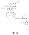
- Figures 1a and 1b provides an illustration of an apparatus suitable for performing chamber cleaning using an internal energy source or a remote energy source, respectively.
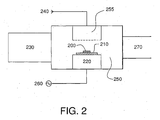
- Figure 2 provides an illustration of an apparatus for performing a process of the invention using plasma as the energy source.
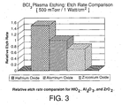
- Figure 3 provides a graphical illustration of the relative BCl 3 plasma etch rates of various high dielectric constant materials, normalized to Al 2 O 3 .
- Figure 4 provides an illustration of an apparatus for performing a process of the invention using thermal heating as the energy source
- Figure 5 provides an illustration of the etch rate dependence on lower electrode/pedestal set temperature at constant chamber pressure and BCl 3 flow rate.
- Figure 6 provides an illustration of the etch rate dependence on chamber pressure at constant lower electrode set temperature and BCl 3 flow rate.
- Figures 7a through 7c illustrate the HfO 2 , HfSi x O y , and ZrO 2 etch rates, respectively, at different NF 3 percentages in the mixture of BCl 3 and NF 3 for one embodiment of the present invention.
- the present process is useful for dry-etching high-k materials and dry-cleaning chemical vapor deposition (CVD) chambers (and more specifically, ALDchambers) used to deposit high-k materials onto wafer surfaces.
- the material to be removed from the surface being etched or cleaned is converted from a solid non-volatile material into materials having higher volatility than the high-k materials deposited thereupon and can be subsequently removed, for example, by reactor vacuum pumps.
- the invention removes a substance from a substrate using one or more reactive agents to volatilize the substance.
- dry-etching and dry-cleaning processes do not immerse the substrate in or expose the substrate to liquid chemical solutions.
- the substance to be removed can be a transition metal oxide, a transition metal silicate, a Group 13 metal oxide or a Group 13 metal silicate (in accordance with the IUPAC Nomenclature of Inorganic Chemistry, Recommendations 1990, Group 13 metals include Al, Ga, In and TI, and the transition metals occupy Groups 3-12).
- the substance may be a high-k material having a dielectric constant greater than that of silicon dioxide (i.e., greater than about 4.1), or greater than 5, or at least 7.
- the substance is at least one member selected from the group consisting of Al 2 O 3 , HfO 2 , ZrO 2 , HfSi x O y , ZrSi x O y , and mixtures thereof.
- HfSi x O y (and the formula ZrSi x O y ) represents a mixture of HfO 2 (ZrO 2 ) and SiO 2 , where x is greater than 0 and y is 2x + 2.
- the substance may be a laminate comprising layers of at least one member selected from the group of the following materials: a transition metal oxide, a transition metal silicate, a Group 13 metal oxide, a Group 13 metal silicate, a nitrogen containing transition metal oxide, a nitrogen containing transition metal silicate, a nitrogen containing Group 13 metal oxide, or a nitrogen containing Group 13 metal silicate.
- the laminate is preferably alternating between at least one of the foregoing materials and, optionally, other materials such as insulating materials.
- the laminate may be comprised of alternating layers of HfO 2 and Al 2 O 3 .
- the laminate may also consist of a certain number of layers of a first material and a certain number of layers of a second material or, alternatively, outer layers of at least one first material and inner layers of at least one second material.
- the substance may be a nitrogen containing material such as a nitrogen containing transition metal oxide, a nitrogen containing transition metal silicate, a nitrogen containing Group 13 metal oxide, or a nitrogen containing Group 13 metal silicate.
- a nitrogen containing material such as a nitrogen containing transition metal oxide, a nitrogen containing transition metal silicate, a nitrogen containing Group 13 metal oxide, or a nitrogen containing Group 13 metal silicate.
- An example of this type of substance includes HfAlON.
- the substance to be removed is reacted with a reactive agent to form a volatile product which can be readily removed from the substrate.
- the reactive agent may be exposed to one or more energy sources sufficient to form active species such as ions, radicals, excited neutrals, and the like, which react with the substance and form the volatile product.
- Suitable reactive agents include: a halogen-containing compound such as a chloride, bromide, fluoride, or iodide compound; a boron-containing compound, a carbon-containing compound, a hydrogen-containing compound, a nitrogen-containing compound , a chelating compound, a chlorosilane compound, a hydrochlorosilane compound, an organochlorosilane compound, or a mixture thereof.
- the reactive agents can be delivered to the reaction chamber by a variety of means, such as, for example, conventional cylinders, safe delivery systems, vacuum delivery systems, solid or liquid-based generators that create the reactive agent at the point of use.
- at least one reactive agent can be added to a non-reactive liquid or gaseous diluent and applied to the substrate having the substance to be removed as a spray or other means.
- the reactive agent can react with the substance to form the volatile product upon exposure to one or more energy sources.
- the reactive agent(s) can be deposited onto a non-reactive support which can be introduced into the reaction chamber.
- the material of the non-reactive support is one that will not react with the reactive agent prior to or during exposure to one of energy sources.
- the non-reactive support has a plurality of pores. The reactive agent(s) can be released upon exposure to one or more energy sources and react with the substance to be removed to form the volatile product.
- chlorides of these metals are more volatile, it may be preferrable to convert these high-k substances into chlorides. This conversion is accomplished by contacting the substance to be removed with a reactive agent containing chlorine.
- chlorine-containing reactive agents examples include BCl 3 , COCl 2 , HCl, Cl 2 , ClF 3 , and NF z Cl 3-z , where z is an integer from 0 to 2, chlorocarbons, and chlorohydrocarbons (such as C x H y Cl z where x is a number ranging from 1 to 6, y is a number ranging from 0 to 13, and z is a number ranging from 1 to 14).
- Chlorine-containing reactive agents that also contain oxygen-getter functions may be suitable in certain embodiments because the oxygen-getter component (B, CO, C, or H) in these molecules extracts oxygen from the high-k materials and hence enhances the conversion of metal oxides and metal silicates into metal chlorides.
- BCl 3 is the most preferred one.
- COCl 2 as the reactive agent it can be provided in prepared form or formed by an in situ reaction of CO and Cl 2 .
- the reactive agent can comprise a chlorine-containing gas and a fluorine-containing gas (e.g., BCl 3 and BF 3 ), or a gas containing both fluorine and chlorine such as ClF 3 , and NF 2 Cl 3-z , where z is an integer from 0 to 2.
- a fluorine-containing gas e.g., BCl 3 and BF 3
- a gas containing both fluorine and chlorine such as ClF 3 , and NF 2 Cl 3-z , where z is an integer from 0 to 2.
- one or more chlorine-containing reactive agents can be combined with one or more other halogen-containing compounds such as one or more fluorine-containing reactive agents to aid in etching and removing high-k materials.
- fluorides of transition metals such HfF 4 and ZrF 4 are less volatile than the corresponding chlorides, it is surprising and unexpected that adding at least one fluorine-containing reactive agent to chlorine-containing reactive agent may enhance the etch rate of high dielectric constant transition metal oxides.
- the gaseous mixture may comprise less than 50% by volume of at least one fluorine-containing reactive agent; at least one chlorine-containing reactive agent; and optionally inert diluent gas.
- An exemplary gas mixture may comprise from about 1 % to less than 50% by volume of at least one fluorine-containing compound and from about 50% to about 99% by volume of at least one chlorine-containing compound.
- the fluorine-containing reactive agent(s) may be combined with the chlorine-containing reactive agent(s) to provide the mixture prior to or after introduction to the reactor.
- fluorine-containing reactive agents include NF 3 (nitrogen trifluoride), ClF 3 (chlorine trifluoride), CIF (chlorine fluoride), SF 6 (sulfur hexafluoride), perfluorocarbons such as CF 4 and C 2 F 6 etc, hydrofluorocarbons such as CHF 3 and C 3 F 7 H etc., oxyfluorocarbons such as C 4 F 8 O (perfluorotetrahydrofuran) etc., hypofluorites such as CF 3 -OF (fluoroxytrifluoromethane (FTM)) and FO-CF 2 -OF (bis-difluoroxy-difluoromethane (BDM)) etc., fluoroperoxides such as CF 3 -O-O-CF 3 , F-O-O-F etc., fluorotrioxides such as CF 3 -O-O-O-CF 3 etc., COF 2 (carbonyl flouride), NOF
- Exemplary gaseous mixtures include, but are not limited to, BCl 3 and NF 3 ; BCl 3 and F 2 ; BCl 3 and CIF 3 ; BCl 3 and NF x Cl 3-x where x is an integer from 1 to 2.
- Other Cl-, Br-, or I- containing compounds such as, for example, any of the compounds disclosed herein, may also have this synergistic effect with the F-containing compounds.
- inert diluent gases such as nitrogen, CO, helium, neon, argon, krypton, and xenon etc. can also be added. Inert diluent gases can modify the plasma characteristics and cleaning processes to better suit some specific applications.
- concentration of the inert gases can range from 0 to 99%.
- etching embodiments of the invention include, e.g., semiconductor wafers and the like.
- Figure 3 shows a comparison of the relative etch rate of hafnium oxide, aluminum oxide, and zirconium oxide for one embodiment of the present invention using BCl 3 as the reactive agent.
- the present invention may be also suitable for cleaning substances from substrates such as surfaces of reaction chambers for CVD and/or ALD processes.
- the present invention is particularly suited for removing high k substances that have deposited onto the exposed surfaces of a reaction chamber such as, for example, the workpiece platform, grounded sidewalls, and/or showerhead of a typical reaction chamber.
- the one or more reactive agents are exposed to one or more energy sources sufficient to generate active species to at least partially react with the substance and/or boron-containing by-products and form volatile species.
- the energy source for the exposing step may include, but not be limited to, ⁇ -particles, ⁇ -particles, ⁇ -rays, x-rays, high energy electron, electron beam sources of energy; ultraviolet (wavelengths ranging from 10 to 400 nm), visible (wavelengths ranging from 400 to 750 nm), infrared (wavelengths ranging from 750 to 10 5 nm), microwave (frequency > 10 9 Hz), radiofrequency wave (frequency > 10 6 Hz) energy; thermal; RF, DC, arc or corona discharge; sonic, ultrasonic or megasonic energy; and mixtures thereof.
- thermal or plasma activation and/or enhancement can significantly impact the efficacy of dry etching and dry cleaning of high dielectric constant materials.
- the substrate can be heated up to 600°C, or up to 400°C, or up to 300°C.
- the pressure range is generally 10 mTorr to 760 Torr, or 1 Torr to 760 Torr.
- the reactive agent(s) are activated by a plasma in situ or within the reactor containing the substance to be removed.
- a plasma in situ or within the reactor containing the substance to be removed For in situ plasma activation, one can generate the plasma with a 13.56 MHz RF power supply, with RF power density at least 0.2 W/cm 2 , or at least 0.5 W/cm 2 , or at least 1 W/cm 2 .
- the operating pressure is generally in the range of 2.5 mTorr to 100 Torr, or 5 mTorr to 50 Torr, or 10 mTorr to 20 Torr.
- thermal and plasma enhancement for more effective cleaning of ALD chamber walls.
- the remote plasma source can be generated by either an RF or a microwave source.
- reactions between remote plasma generated reactive species and high-k materials can be activated/enhanced by heating ALD reactor components to elevated temperatures up to 600°C, or to 400°C, or up to 300°C.
- BCl 3 and COCl 2 can be used as the etchants for dry etching and cleaning of the high-k materials.
- BCl 3 boron trichloride
- COCl 2 phosgene
- phosgene is preferably provided in situ in etch or deposition reactors by reacting gaseous carbon monoxide and chlorine to form phosgene assisted by an external energy source (e.g. plasma) as follows: CO (g) + Cl 2 (g) ⁇ COCl 2
- chlorocarbons CC
- HCC hydrochlorocarbons
- CC and HCC compounds may be employed as the reactive agent because these compounds may contain chlorine as well as oxygen getter components (C or H).
- the general formula for the CC and HCC compounds is C x H y Cl z , where x ranges from 1 to 6, y ranges from 0 to 13, and z ranges from 1 to 14.
- suitable CC and HCC compounds include, but are not limited to, trans-dichloroethylene C 2 H 2 Cl 2 (a.k.a.
- Trans-LC® cis-dichloroethylene, 1,1-dichloroethylele, 1,1,1-trichloroethane (C 2 H 3 Cl 3 ), or tetrachloroethylene C 2 Cl 4 , C 4 H 4 Cl 4 , CHCl 3 , and CCl 4.
- Some CC and HCC compounds may react with high-k metal oxides without the addition of oxygen.
- tetrachloroethylene (C 2 Cl 4 ) can react with Al 2 O 3 to form volatile byproducts as follows: 1.5C 2 Cl 4 (g) + Al 2 O 3 ⁇ 2AlCl 3 (g) + 3CO(g)
- Table 8 illustrates that the reaction is thermodynamically favorable at temperatures above 100 °C.
- Thermodynamic data for reaction: 1.5C 2 Cl 4 (g) + Al 2 O 3 2AlCl 3 (g) + 3CO(g) T (°C) ⁇ H (kcal) ⁇ S (cal) ⁇ G (kcal) K eq 0.000 46.723 157.382 3.734 1.028E-003 100.000 46.760 157.552 -12.031 1.114E+007 200.000 46.314 156.508 -27.738 6.509E+012 300.000 45.599 155.144 -43.322 3.317E+016 400.000 44.704 153.709 -58.765 1.204E+019 500.000 43.674 152.284 -74.064 8.667E+020 600.000 42.541 150.907 -89.223 2.160E+022 700.000 41.340 149.605 -104.248 2.594E+023 800.000 40.087 148.380
- thermochemical calculations are illustrations of limiting cases for those chemical reactions.
- intermediate reaction products such as boron oxychloride (BOCl) can also be formed in reactions between high-k materials and BCl 3 .
- Intermediate reaction products such as BOCI may have higher volatility and thus may further enhance the removal of high-k materials.
- CC and HCC compounds may need the addition of oxygen to release chlorine without forming carbon residues (soot).
- trans-dichloroethylene C 2 H 2 Cl 2
- Trans-LC® trans-dichloroethylene
- Table 9 shows such a reaction is thermodynamically favorable at temperatures between 0 and 1000 °C.
- Both reactions are thermodynamically favorable, as shown in Tables 11 and 12.
- the bromide and iodide compounds of these high-k materials such as AlBr 3 , AlI 3 , HfBr 4 , Hfl 4 , ZrBr 4 , and ZrI 4 have volatility similar to their corresponding chlorides. Therefore, some bromo- and iodo-compounds can also be used to etch/clean these high-k materials. Bromine and iodine ions are heavier than chlorine ions, hence bromine and iodine ions can provide more effective sputtering to energize plasma-assisted etch/clean reactions with high-k materials. Bromine and iodine atoms have higher surface sticking coefficients than chlorine atoms.
- a higher sticking coefficient relates to a higher probability for bromine and iodine atoms/ions to be adsorbed onto the surface of high-k materials hence enhancing the bromination/iodization reactions.
- Desirable bromo- and iodo-compounds may contain an oxygen-getter function in the molecule.
- bromine and iodine containing compounds examples include boron tribromide (BBr 3 ), boron triiodide (Bl 3 ), hydrogen bromide (HBr), hydro iodide (Hl), bromocarbons such as CBr 4 , bromohydrocarbons such as trans-dibromoethylene (C 2 H 2 Br 2 ), iodocarbons such as Cl 4 , and iodohydrocarbons such as trans-diiodoethylene (C 2 H 2 I 2 ) etc.
- BBr 3 boron tribromide
- Bl 3 hydrogen bromide
- Hl hydro iodide
- bromocarbons such as CBr 4
- bromohydrocarbons such as trans-dibromoethylene (C 2 H 2 Br 2 )
- iodocarbons such as Cl 4
- iodohydrocarbons such as trans-diiodoethylene (C 2 H
- bromine and iodine chemistries are also thermodynamically favorable for reactions with Al 2 O 3 and ZrO 2 , as shown in Tables 16-18.
- Thermodynamic data for reaction: 2BBr 3 (g) + Al 2 O 3 2AlBr 3 (g) + B 2 O 3 T (°C) ⁇ H (kcal) ⁇ S (kcal) ⁇ G (kcal) K eq 0.000 -2.212 12.687 -5.678 3.493E+004 100.000 -2.279 12.503 -6.944 1.168E+004 200.000 -2.482 12.022 -8.170 5.945E+003 300.000 -2.685 11.632 -9.352 3.683E+003 400.000 -2.852 11.362 -10.501 2.567E+003 500.000 3.023 19.476 -12.035 2.525E+003 600.000 3.337 19.858 -14.003 3.200E+003 700.000 3.579 20.122 -16
- the reactive agent may comprise a chelating compound.
- a chelating compound describes a compound that contains at least two electron-rich (e.g., Lewis base) sites that could potentially interact with an electron-deficient (e.g., Lewis acid) metal atom such as, but not limited to, Zr, Al, or Hf. It is not required, however, that the plurality of sites simultaneously interact with the metal in order.
- the chelating compound may be delivered into the reaction chamber as a conjugate acid of the basic site. Examples of these compounds may be found in U. S. Pat. No. 3,634,477.
- chelating compounds include oxy-halocarbon compounds, such as chloroacetic acid, oxalyl chloride, etc., are known to be chelating compounds or agents that can react with metal oxides and metal chlorides to form volatile byproducts.
- Some exemplary chelating compounds may have the formula C ⁇ H ⁇ X ⁇ Y ⁇ O ⁇ , wherein X and Y are one of the halogen atoms F, Cl, Br, and I; ⁇ is a number ranging from 1 to 6, ⁇ is a number ranging from 0 to 13, the sum of y+ ⁇ is a number ranging from 1 to 14, and ⁇ is a number ranging from 1 to 6.
- Examples of these compounds include hexafluoropetanedione (CCl 3 C(O)CH 2 C(O)CCl 3 ) (a.k.a. Hhfac), hexachloropetanedione (CCl 3 C(O)CH 2 C(O)CCl 3 ), hexafluoroacetone (CF 3 C(O)CF 3 ) and hexachloroacetone (CCl 3 C(O)CCl 3 ).
- hexafluoropetanedione a.k.a.
- Hhfac (CF 3 C(O)CH 2 C(O)CF 3 , or C 5 H 2 O 2 F 6 ) is a common chelating agent that can react with a wide variety of metal oxides and/or chlorides to form volatile organo-metal compounds M(hfac) x , where M is a metal ion such as Al 3+ , Hf 4+ , and Zr 4+ etc.
- M is a metal ion such as Al 3+ , Hf 4+ , and Zr 4+ etc.
- Such chelating property can be used to enhance the etching and chamber cleaning of high-k materials.
- these molecules can be used as an oxygen scavenger to enhance chlorination of the high-k materials.
- HfO 2 + C 5 H 2 O 2 F 6 + 2Cl 2 + O 2 HfCl 4 (g) + H 2 O(g) + 3COF 2 (g) + 2CO(g)
- the chlorine analog of Hhfac, hexachloropetanedione (CCl 3 C(O)CH 2 C(O)CCl 3 ) may be more advantageous as the reactive agent since it can be both an oxygen scavenger and a chlorinating agent.
- These reactions can be also be assisted by thermal and/or plasma activation.
- chlorine can be used to replace oxygen:
- C 5 H 2 O 2 Cl 6 + Al 2 O 3 + Cl 2 2AlCl 3 (g) + 5CO(g) + 2HCl(g)
- chlorosilanes, hydrochlorosilane, and organochlorosilanes can also be effective agents to etch/clean high-k materials. Due in part to the highly stable SiO 2 byproduct, these compounds may be both a very effective oxygen scavenger and a chlorinating agent. Upon exposure to a thermal or plasma source, these compounds may be just as effective as BCl 3 to convert high-k materials into volatile chlorides without the potential problem of boron residue contamination.
- the chlorosilane, hydrochlorosilane, or organochlorosilane compound has the formula Si p Cl q R s H t , wherein: 1 ⁇ p ⁇ 3, 1 ⁇ q ⁇ ⁇ 2p + 2 - (s+t) ⁇ , s and t can have any values subject to the constraint that 0 ⁇ (s + t) ⁇ (2p + 1) and R is an organic radical having 1-8 carbon atoms, including: hydrocarbyl (e.g.
- halocarbyl e.g., trichloromethyl, trifluoromethyl, pentafluoroethyl
- halogenated hydrocarbyl e.g., chloromethyl, 2, 4-difluorophenyl
- oxygenated hydrocarbyl e.g., methoxy, hydroxyethyl, chlorormethoxy
- nitrogen-substituted hydrocarbyl moieties e.g., aminomethyl, dimethylaminonomethyl, pyridyl.
- Thermodynamic calculations show that the above reactions are favorable at room temperature or moderately elevated temperatures, as shown in Tables 19-23.
- chloride compounds such as GeCl 4 and related compounds can also be used to etch/clean high-k materials in a similar manner.
- AlCl 3 can be added into the reactants to enhance the chlorination of HfO 2 , ZrO 2 , HfSi x O y , and ZrSi x O y etc. This is because AlCl 3 can be used as an oxygen scavenger to facilitate the chlorination of HfO 2 and ZrO 2 etc. while forming aluminum oxychloride such as AIOCI, which is more volatile than Al 2 O 3 .
- a chemical reaction In addition to being thermodynamically favorable, a chemical reaction often requires an external energy source to overcome an activation energy barrier so that the reaction can proceed.
- the external energy source can be, for example, thermal heating or plasma activation. Higher temperatures can accelerate chemical reactions and make reaction byproducts more volatile.
- temperature in production deposition chambers Plasmas can generate more reactive species to facilitate reactions. Ions in the plasmas are accelerated by the electric field in the plasma sheath to gain energy. Energetic ions impinging upon surfaces can provide the energy needed to overcome reaction activation energy barrier. Ion bombardments also helps to volatize and remove reaction byproducts. These are common mechanisms in plasma etching/cleaning and reactive ion etching.
- reactions between remote plasma generated reactive species and high-k materials can be activated and/or enhanced by heating CVD or ALD reactor components to elevated temperatures up to 600 °C, or to 400 °C, and or up to 300 °C.
- Figures 1a and 1b provides an illustration of an apparatus 10 suitable for performing chamber cleaning using an internal energy source such as an in-situ plasma or a thermal source or an external energy source, respectively.
- the reactive agent 20 i.e., BCl 3
- the substrate 30 i.e., reaction chamber
- the substance 40 is deposited upon at least a portion of the exposed surface within the reaction chamber 30, particularly, the grounded sidewalls 32, showerhead 34, work piece platform 36, etc.
- the reactive agent 20 is exposed to an external energy source 50, such as the RF power supply or heater shown, which creates active species 60 such as BCl 3 and Cl shown by the dashed arrows.
- active species 60 such as BCl 3 and Cl shown by the dashed arrows.
- the active species 60 react with substance 40 and form a volatile product 70 such as HfCl 4 .
- the volatile product 70 is removed from the chamber 30 as shown by the dotted arrows.
- Figure 1b provides an example of an apparatus 100 wherein the reactive agent 120 (i.e., BCl 3 ) is exposed to an external energy source 150 such as a microwave source to produce a high density plasma 110 of the reactive agent within an applicator/resonant cavity 115.
- the high density plasma 110 can then be transported to the substrate 130 (i.e., reaction chamber) having the substance to be removed (not shown) and form the volatile product (not shown).
- the volatile product can be easily removed from the chamber 130 via the foreline shown 140 and assisted by pump 160.
- Reactor 250 is connected to a turbo pump (not shown) through line 270.
- the thickness of the high-k film on a coupon was measured by ellipsometry both before and after a timed exposure of the processing plasma. Change in high-k film thickness after plasma processing is used to calculate the etch rate. In addition to etch rate, plasma dc self bias voltage (V bias ) was also measured. In examples 1-3, both the wafer and the chamber walls were kept at room temperature.
- Example 1 Plasma etching/cleaning of Al 2 O 3 samples
- threshold power density 0.55 W/cm 2 or threshold V bias of 35 V for etching Al 2 O 3 .
- Higher power density and higher V bias resulted in higher etch rate.
- Tables 24 and 25 show, for example, that higher power and lower pressure can increase bias voltage, which in turn may enhance chemical etching of high-k materials. Lower pressure and higher power is particularly effective to enhance plasma etching of substrates coated with high-k films.
- Example 2 Plasma etching/cleaning of HfO 2 samples
- Example 3 Plasma etching/cleaning of ZrO 2 samples
- Figure 3 shows the relative comparison of BCl 3 plasma etch rates of high-k materials HfO 2 , Al 2 O 3 , and ZrO 2 at 500 mTorr chamber pressure and 1 W/cm 2 RF power density. It can be seen that HfO 2 has the highest etch rate, and ZrO 2 has the lowest etch rate among the three high-k materials.
- Examples 4 and 5 illustrate BCl 3 thermal etching/cleaning of high-k materials.
- Figure 4 is a schematic of the experimental setup for examples 4 and 5.
- RF power 310 can be applied on the top electrode 320, and the lower electrode 330 and the chamber walls 340 are grounded.
- This reactor can be operated with both RF plasma and thermal heating during an etching/cleaning experiments. Only thermal heating was used in examples 4 and 5.
- the lower electrode/pedestal 330 can be heated by an AC powered heater 350 and controlled by the temperature controller 360.
- the temperature range of the lower electrode/pedestal 330 is from room temperature up to 700°C.
- the sample 360 and the carrier wafer 370 were placed on the lower electrode/pedestal 330.
- Sample surface temperature is about 50°C lower than the lower electrode set point in ambient atmosphere. Sample preparation and measurement procedures were similar to those in examples 1 through 3. After sample introduction, the reactor was evacuated, and the heater 350 was turned on. When the lower electrode 330 reached the set point, process gases 380 were introduced into the chamber 300 to reach a set pressure. The sample was exposed to the process gases 380 for a set period of time. The process gases 380 were evacuated through line 390 that connects to a pump (not shown) and the sample 360 was retrieved from the reactor chamber 300 for measurement.
- Example 4 Thermal etching/cleaning of Al 2 O 3 samples
- Example 5 Thermal etching/cleaning of HfO 2 samples
- Figure 5 examines the etch rate dependence on lower electrode temperature at constant chamber pressure and BCl 3 flow rate. It can be seen that both Al 2 O 3 and HfO 2 etch rates increase at temperature increases. The etch rates of HfO 2 are higher than those of Al 2 O 3 under the same conditions.
- Figure 6 examines the etch rate dependence on chamber pressure at constant lower electrode set temperature and BCl 3 flow rate. It can be seen that etch rates increase at higher pressures. At lower electrode temperature about 350°C, increasing chamber pressure is a more effective method to enhance etch rates. Again, the etch rates of HfO 2 are higher than those of Al 2 O 3 under the.same conditions.
- Comparative Example 1 NF 3 plasma etching/cleaning of Al 2 O 3 , HfO 2 , and ZrO 2 samples
- a lower chamber pressure may also lead to faster desorption and diffusion of reaction byproducts.
- the NF 3 plasma had significantly lower etch rates for either the Al 2 O 3 , the HfO 2 , or the ZrO 2 samples.
- Example 6 Plasma Etching/Cleaning of HfO 2 , ZrO 2 , and HfSi x O y samples using a mixture of BCl 3 and NF 3
- a mixture of BCl 3 and NF 3 was used to test the etch rates of three different high-k materials, HfO 2 , ZrO 2 , and HfSi x O y .
- HfO 2 the flow rate of BCl 3 was 10 sccm and the flow rate of NF 3 was adjusted to obtain different NF 3 to BCl 3 volumetric ratios.
- ZrO 2 and HfSi x O y the total flow rate was 20 sccm and the flow rates of BCl 3 and NF 3 were adjusted accordingly to obtain different NF 3 to BCl 3 volumetric ratios.
- the power density was 0.55 W/cm 2 and the chamber pressure was 500 mTorr. The experiments were run using the same set-up as shown in Figure 2 and following the same method as Examples 1 through 3 and Comparative Example 1.
- Figures 7a through 7c illustrate the relationship between the volumetric percentage of NF 3 in the BCl 3 and NF 3 mixture and etch rates for HfO 2 , HfSi x O y , ZrO 2 , respectively.
- the etch rates for HfO 2 (shown in Figure 7a) and for HfSi x O y (shown in Figure 7b) were almost doubled at about 25% by volume NF 3 and 15% by volume NF 3 , respectively.
- Figure 7c shows the etch rates of ZrO 2 at different NF 3 additions to BCl 3 .
- BCl 3 cannot remove the ZrO 2 material under the given plasma condition: 0.55 W/cm 2 power density and 500 mTorr reactor chamber pressure.
- the thickness of ZrO 2 was increased after 1-minute exposure to the BCl 3 plasma.
- Etching occurs with addition of NF 3 .
Landscapes
- Chemical & Material Sciences (AREA)
- Physics & Mathematics (AREA)
- Optics & Photonics (AREA)
- General Chemical & Material Sciences (AREA)
- Chemical Kinetics & Catalysis (AREA)
- Engineering & Computer Science (AREA)
- Materials Engineering (AREA)
- Mechanical Engineering (AREA)
- Metallurgy (AREA)
- Organic Chemistry (AREA)
- Drying Of Semiconductors (AREA)
- Cleaning Or Drying Semiconductors (AREA)
Applications Claiming Priority (2)
| Application Number | Priority Date | Filing Date | Title |
|---|---|---|---|
| US723714 | 2003-11-26 | ||
| US10/723,714 US7357138B2 (en) | 2002-07-18 | 2003-11-26 | Method for etching high dielectric constant materials and for cleaning deposition chambers for high dielectric constant materials |
Publications (1)
| Publication Number | Publication Date |
|---|---|
| EP1538235A1 true EP1538235A1 (de) | 2005-06-08 |
Family
ID=34465714
Family Applications (1)
| Application Number | Title | Priority Date | Filing Date |
|---|---|---|---|
| EP04027638A Withdrawn EP1538235A1 (de) | 2003-11-26 | 2004-11-22 | Verfahren zum Ätzen von Werkstoffen mit hoher Dielektrizitätskonstante und Verfahren zur Reiningung eines Abscheidungskammer von Werkstoffen mit hoher Dielektrizitätskonstante |
Country Status (7)
| Country | Link |
|---|---|
| US (1) | US7357138B2 (de) |
| EP (1) | EP1538235A1 (de) |
| JP (1) | JP2005175466A (de) |
| KR (1) | KR100667723B1 (de) |
| CN (1) | CN100372055C (de) |
| SG (2) | SG112101A1 (de) |
| TW (1) | TWI267898B (de) |
Families Citing this family (595)
| Publication number | Priority date | Publication date | Assignee | Title |
|---|---|---|---|---|
| JP2004225152A (ja) * | 2003-01-27 | 2004-08-12 | Tokyo Electron Ltd | 基板処理方法および半導体装置の製造方法 |
| EP1629529A2 (de) * | 2003-05-30 | 2006-03-01 | Tokyo Electron Limited | Verfahren und system zum ätzen eines dielektrischen materials mit hohem k |
| US20050153563A1 (en) * | 2004-01-14 | 2005-07-14 | Lam Research Corporation | Selective etch of films with high dielectric constant |
| JP2005268292A (ja) * | 2004-03-16 | 2005-09-29 | Toshiba Corp | 半導体装置の製造方法 |
| US20050241671A1 (en) * | 2004-04-29 | 2005-11-03 | Dong Chun C | Method for removing a substance from a substrate using electron attachment |
| US20050241670A1 (en) * | 2004-04-29 | 2005-11-03 | Dong Chun C | Method for cleaning a reactor using electron attachment |
| US7581549B2 (en) * | 2004-07-23 | 2009-09-01 | Air Products And Chemicals, Inc. | Method for removing carbon-containing residues from a substrate |
| US20060017043A1 (en) * | 2004-07-23 | 2006-01-26 | Dingjun Wu | Method for enhancing fluorine utilization |
| US7179759B2 (en) * | 2004-09-30 | 2007-02-20 | Taiwan Semiconductor Manufacturing Company | Barrier layer and fabrication method thereof |
| JP4836112B2 (ja) * | 2004-12-24 | 2011-12-14 | 国立大学法人京都大学 | 半導体処理装置のクリーニング方法およびシリコン基板のエッチング方法 |
| US7509962B2 (en) * | 2005-01-21 | 2009-03-31 | Tokyo Electron Limited | Method and control system for treating a hafnium-based dielectric processing system |
| US20060183055A1 (en) * | 2005-02-15 | 2006-08-17 | O'neill Mark L | Method for defining a feature on a substrate |
| US7485580B2 (en) * | 2005-09-20 | 2009-02-03 | Air Products And Chemicals, Inc. | Method for removing organic electroluminescent residues from a substrate |
| US20080047579A1 (en) * | 2006-08-25 | 2008-02-28 | Bing Ji | Detecting the endpoint of a cleaning process |
| US8986456B2 (en) * | 2006-10-10 | 2015-03-24 | Asm America, Inc. | Precursor delivery system |
| KR101064354B1 (ko) * | 2006-11-09 | 2011-09-14 | 가부시키가이샤 알박 | 장벽막 형성 방법 |
| JP5110987B2 (ja) * | 2007-07-05 | 2012-12-26 | 株式会社日立ハイテクノロジーズ | プラズマ処理方法およびコンピュータ読み取り可能な記録媒体 |
| JP5297615B2 (ja) * | 2007-09-07 | 2013-09-25 | 株式会社日立ハイテクノロジーズ | ドライエッチング方法 |
| JP2009076590A (ja) * | 2007-09-19 | 2009-04-09 | Hitachi Kokusai Electric Inc | クリーニング方法 |
| JP5213868B2 (ja) * | 2007-09-19 | 2013-06-19 | 株式会社日立国際電気 | クリーニング方法及び基板処理装置 |
| JP4994197B2 (ja) * | 2007-11-16 | 2012-08-08 | 株式会社日立国際電気 | 半導体装置の製造方法及び基板処理装置 |
| JP5226452B2 (ja) * | 2008-10-09 | 2013-07-03 | 大日本スクリーン製造株式会社 | チャンバ洗浄方法 |
| US20100112191A1 (en) * | 2008-10-30 | 2010-05-06 | Micron Technology, Inc. | Systems and associated methods for depositing materials |
| US10378106B2 (en) | 2008-11-14 | 2019-08-13 | Asm Ip Holding B.V. | Method of forming insulation film by modified PEALD |
| US9394608B2 (en) | 2009-04-06 | 2016-07-19 | Asm America, Inc. | Semiconductor processing reactor and components thereof |
| US20100273291A1 (en) * | 2009-04-28 | 2010-10-28 | Applied Materials, Inc. | Decontamination of mocvd chamber using nh3 purge after in-situ cleaning |
| WO2010129289A2 (en) * | 2009-04-28 | 2010-11-11 | Applied Materials, Inc. | Decontamination of mocvd chamber using nh3 purge after in-situ cleaning |
| US8883270B2 (en) * | 2009-08-14 | 2014-11-11 | Asm America, Inc. | Systems and methods for thin-film deposition of metal oxides using excited nitrogen—oxygen species |
| US8802201B2 (en) | 2009-08-14 | 2014-08-12 | Asm America, Inc. | Systems and methods for thin-film deposition of metal oxides using excited nitrogen-oxygen species |
| US8877655B2 (en) | 2010-05-07 | 2014-11-04 | Asm America, Inc. | Systems and methods for thin-film deposition of metal oxides using excited nitrogen-oxygen species |
| CN102414801A (zh) * | 2009-08-27 | 2012-04-11 | 应用材料公司 | 在原位腔室清洁后的处理腔室去污方法 |
| US8778464B2 (en) * | 2009-11-04 | 2014-07-15 | Tel Solar Ag | Method of removing contamination from a reactor |
| JP5655296B2 (ja) * | 2009-12-01 | 2015-01-21 | セントラル硝子株式会社 | エッチングガス |
| US9324576B2 (en) | 2010-05-27 | 2016-04-26 | Applied Materials, Inc. | Selective etch for silicon films |
| US8901016B2 (en) * | 2010-12-28 | 2014-12-02 | Asm Japan K.K. | Method of forming metal oxide hardmask |
| US10283321B2 (en) | 2011-01-18 | 2019-05-07 | Applied Materials, Inc. | Semiconductor processing system and methods using capacitively coupled plasma |
| US8999856B2 (en) | 2011-03-14 | 2015-04-07 | Applied Materials, Inc. | Methods for etch of sin films |
| US9064815B2 (en) | 2011-03-14 | 2015-06-23 | Applied Materials, Inc. | Methods for etch of metal and metal-oxide films |
| US9312155B2 (en) | 2011-06-06 | 2016-04-12 | Asm Japan K.K. | High-throughput semiconductor-processing apparatus equipped with multiple dual-chamber modules |
| US9793148B2 (en) | 2011-06-22 | 2017-10-17 | Asm Japan K.K. | Method for positioning wafers in multiple wafer transport |
| US10364496B2 (en) | 2011-06-27 | 2019-07-30 | Asm Ip Holding B.V. | Dual section module having shared and unshared mass flow controllers |
| US10854498B2 (en) | 2011-07-15 | 2020-12-01 | Asm Ip Holding B.V. | Wafer-supporting device and method for producing same |
| US20130023129A1 (en) | 2011-07-20 | 2013-01-24 | Asm America, Inc. | Pressure transmitter for a semiconductor processing environment |
| US8808563B2 (en) | 2011-10-07 | 2014-08-19 | Applied Materials, Inc. | Selective etch of silicon by way of metastable hydrogen termination |
| US9341296B2 (en) | 2011-10-27 | 2016-05-17 | Asm America, Inc. | Heater jacket for a fluid line |
| US9096931B2 (en) | 2011-10-27 | 2015-08-04 | Asm America, Inc | Deposition valve assembly and method of heating the same |
| US9017481B1 (en) | 2011-10-28 | 2015-04-28 | Asm America, Inc. | Process feed management for semiconductor substrate processing |
| US9167625B2 (en) | 2011-11-23 | 2015-10-20 | Asm Ip Holding B.V. | Radiation shielding for a substrate holder |
| US9005539B2 (en) | 2011-11-23 | 2015-04-14 | Asm Ip Holding B.V. | Chamber sealing member |
| US9202727B2 (en) | 2012-03-02 | 2015-12-01 | ASM IP Holding | Susceptor heater shim |
| US8946830B2 (en) | 2012-04-04 | 2015-02-03 | Asm Ip Holdings B.V. | Metal oxide protective layer for a semiconductor device |
| US9029253B2 (en) | 2012-05-02 | 2015-05-12 | Asm Ip Holding B.V. | Phase-stabilized thin films, structures and devices including the thin films, and methods of forming same |
| US8728832B2 (en) | 2012-05-07 | 2014-05-20 | Asm Ip Holdings B.V. | Semiconductor device dielectric interface layer |
| US8933375B2 (en) | 2012-06-27 | 2015-01-13 | Asm Ip Holding B.V. | Susceptor heater and method of heating a substrate |
| US9267739B2 (en) | 2012-07-18 | 2016-02-23 | Applied Materials, Inc. | Pedestal with multi-zone temperature control and multiple purge capabilities |
| US9558931B2 (en) | 2012-07-27 | 2017-01-31 | Asm Ip Holding B.V. | System and method for gas-phase sulfur passivation of a semiconductor surface |
| US9117866B2 (en) | 2012-07-31 | 2015-08-25 | Asm Ip Holding B.V. | Apparatus and method for calculating a wafer position in a processing chamber under process conditions |
| US9373517B2 (en) | 2012-08-02 | 2016-06-21 | Applied Materials, Inc. | Semiconductor processing with DC assisted RF power for improved control |
| US9169975B2 (en) | 2012-08-28 | 2015-10-27 | Asm Ip Holding B.V. | Systems and methods for mass flow controller verification |
| US9659799B2 (en) | 2012-08-28 | 2017-05-23 | Asm Ip Holding B.V. | Systems and methods for dynamic semiconductor process scheduling |
| US9021985B2 (en) | 2012-09-12 | 2015-05-05 | Asm Ip Holdings B.V. | Process gas management for an inductively-coupled plasma deposition reactor |
| US9034770B2 (en) | 2012-09-17 | 2015-05-19 | Applied Materials, Inc. | Differential silicon oxide etch |
| US9023734B2 (en) | 2012-09-18 | 2015-05-05 | Applied Materials, Inc. | Radical-component oxide etch |
| US9390937B2 (en) | 2012-09-20 | 2016-07-12 | Applied Materials, Inc. | Silicon-carbon-nitride selective etch |
| US9132436B2 (en) | 2012-09-21 | 2015-09-15 | Applied Materials, Inc. | Chemical control features in wafer process equipment |
| US9324811B2 (en) | 2012-09-26 | 2016-04-26 | Asm Ip Holding B.V. | Structures and devices including a tensile-stressed silicon arsenic layer and methods of forming same |
| US10714315B2 (en) | 2012-10-12 | 2020-07-14 | Asm Ip Holdings B.V. | Semiconductor reaction chamber showerhead |
| US8969212B2 (en) | 2012-11-20 | 2015-03-03 | Applied Materials, Inc. | Dry-etch selectivity |
| US8980763B2 (en) | 2012-11-30 | 2015-03-17 | Applied Materials, Inc. | Dry-etch for selective tungsten removal |
| US9111877B2 (en) | 2012-12-18 | 2015-08-18 | Applied Materials, Inc. | Non-local plasma oxide etch |
| CN104853855B (zh) * | 2012-12-18 | 2020-07-24 | 海星化学有限公司 | 用于薄膜沉积反应器和薄膜层的原位干式清洁的过程和方法 |
| US8921234B2 (en) | 2012-12-21 | 2014-12-30 | Applied Materials, Inc. | Selective titanium nitride etching |
| US9640416B2 (en) | 2012-12-26 | 2017-05-02 | Asm Ip Holding B.V. | Single-and dual-chamber module-attachable wafer-handling chamber |
| US20160376700A1 (en) | 2013-02-01 | 2016-12-29 | Asm Ip Holding B.V. | System for treatment of deposition reactor |
| US8894870B2 (en) * | 2013-02-01 | 2014-11-25 | Asm Ip Holding B.V. | Multi-step method and apparatus for etching compounds containing a metal |
| US10256079B2 (en) | 2013-02-08 | 2019-04-09 | Applied Materials, Inc. | Semiconductor processing systems having multiple plasma configurations |
| US9362130B2 (en) | 2013-03-01 | 2016-06-07 | Applied Materials, Inc. | Enhanced etching processes using remote plasma sources |
| US9040422B2 (en) | 2013-03-05 | 2015-05-26 | Applied Materials, Inc. | Selective titanium nitride removal |
| US9484191B2 (en) | 2013-03-08 | 2016-11-01 | Asm Ip Holding B.V. | Pulsed remote plasma method and system |
| US9589770B2 (en) | 2013-03-08 | 2017-03-07 | Asm Ip Holding B.V. | Method and systems for in-situ formation of intermediate reactive species |
| US20140271097A1 (en) | 2013-03-15 | 2014-09-18 | Applied Materials, Inc. | Processing systems and methods for halide scavenging |
| JP6114636B2 (ja) * | 2013-06-06 | 2017-04-12 | 東京エレクトロン株式会社 | 乾燥装置及び乾燥処理方法 |
| US8993054B2 (en) | 2013-07-12 | 2015-03-31 | Asm Ip Holding B.V. | Method and system to reduce outgassing in a reaction chamber |
| US9493879B2 (en) | 2013-07-12 | 2016-11-15 | Applied Materials, Inc. | Selective sputtering for pattern transfer |
| US9018111B2 (en) | 2013-07-22 | 2015-04-28 | Asm Ip Holding B.V. | Semiconductor reaction chamber with plasma capabilities |
| US9793115B2 (en) | 2013-08-14 | 2017-10-17 | Asm Ip Holding B.V. | Structures and devices including germanium-tin films and methods of forming same |
| US9396934B2 (en) | 2013-08-14 | 2016-07-19 | Asm Ip Holding B.V. | Methods of forming films including germanium tin and structures and devices including the films |
| US9773648B2 (en) | 2013-08-30 | 2017-09-26 | Applied Materials, Inc. | Dual discharge modes operation for remote plasma |
| US9240412B2 (en) | 2013-09-27 | 2016-01-19 | Asm Ip Holding B.V. | Semiconductor structure and device and methods of forming same using selective epitaxial process |
| US9556516B2 (en) | 2013-10-09 | 2017-01-31 | ASM IP Holding B.V | Method for forming Ti-containing film by PEALD using TDMAT or TDEAT |
| US20150111394A1 (en) * | 2013-10-23 | 2015-04-23 | Taiwan Semiconductor Manufacturing Co., Ltd. | Mechanisms for forming uniform film on semiconductor substrate |
| US9576809B2 (en) | 2013-11-04 | 2017-02-21 | Applied Materials, Inc. | Etch suppression with germanium |
| US9520303B2 (en) | 2013-11-12 | 2016-12-13 | Applied Materials, Inc. | Aluminum selective etch |
| US9605343B2 (en) | 2013-11-13 | 2017-03-28 | Asm Ip Holding B.V. | Method for forming conformal carbon films, structures conformal carbon film, and system of forming same |
| US10179947B2 (en) | 2013-11-26 | 2019-01-15 | Asm Ip Holding B.V. | Method for forming conformal nitrided, oxidized, or carbonized dielectric film by atomic layer deposition |
| US9245762B2 (en) | 2013-12-02 | 2016-01-26 | Applied Materials, Inc. | Procedure for etch rate consistency |
| US9396989B2 (en) | 2014-01-27 | 2016-07-19 | Applied Materials, Inc. | Air gaps between copper lines |
| US9385028B2 (en) | 2014-02-03 | 2016-07-05 | Applied Materials, Inc. | Air gap process |
| US10683571B2 (en) | 2014-02-25 | 2020-06-16 | Asm Ip Holding B.V. | Gas supply manifold and method of supplying gases to chamber using same |
| US9499898B2 (en) | 2014-03-03 | 2016-11-22 | Applied Materials, Inc. | Layered thin film heater and method of fabrication |
| US9447498B2 (en) | 2014-03-18 | 2016-09-20 | Asm Ip Holding B.V. | Method for performing uniform processing in gas system-sharing multiple reaction chambers |
| US10167557B2 (en) | 2014-03-18 | 2019-01-01 | Asm Ip Holding B.V. | Gas distribution system, reactor including the system, and methods of using the same |
| US11015245B2 (en) | 2014-03-19 | 2021-05-25 | Asm Ip Holding B.V. | Gas-phase reactor and system having exhaust plenum and components thereof |
| US9299537B2 (en) | 2014-03-20 | 2016-03-29 | Applied Materials, Inc. | Radial waveguide systems and methods for post-match control of microwaves |
| US9299538B2 (en) | 2014-03-20 | 2016-03-29 | Applied Materials, Inc. | Radial waveguide systems and methods for post-match control of microwaves |
| KR20160137967A (ko) * | 2014-03-24 | 2016-12-02 | 아이엠이씨 브이제트더블유 | 프로세스 챔버의 클리닝 방법 |
| US9903020B2 (en) | 2014-03-31 | 2018-02-27 | Applied Materials, Inc. | Generation of compact alumina passivation layers on aluminum plasma equipment components |
| US9404587B2 (en) | 2014-04-24 | 2016-08-02 | ASM IP Holding B.V | Lockout tagout for semiconductor vacuum valve |
| US9309598B2 (en) | 2014-05-28 | 2016-04-12 | Applied Materials, Inc. | Oxide and metal removal |
| US9378969B2 (en) | 2014-06-19 | 2016-06-28 | Applied Materials, Inc. | Low temperature gas-phase carbon removal |
| US9406523B2 (en) | 2014-06-19 | 2016-08-02 | Applied Materials, Inc. | Highly selective doped oxide removal method |
| US9425058B2 (en) | 2014-07-24 | 2016-08-23 | Applied Materials, Inc. | Simplified litho-etch-litho-etch process |
| US10858737B2 (en) | 2014-07-28 | 2020-12-08 | Asm Ip Holding B.V. | Showerhead assembly and components thereof |
| US9496167B2 (en) | 2014-07-31 | 2016-11-15 | Applied Materials, Inc. | Integrated bit-line airgap formation and gate stack post clean |
| US9378978B2 (en) | 2014-07-31 | 2016-06-28 | Applied Materials, Inc. | Integrated oxide recess and floating gate fin trimming |
| US9543180B2 (en) | 2014-08-01 | 2017-01-10 | Asm Ip Holding B.V. | Apparatus and method for transporting wafers between wafer carrier and process tool under vacuum |
| US9659753B2 (en) | 2014-08-07 | 2017-05-23 | Applied Materials, Inc. | Grooved insulator to reduce leakage current |
| US9553102B2 (en) | 2014-08-19 | 2017-01-24 | Applied Materials, Inc. | Tungsten separation |
| US9890456B2 (en) | 2014-08-21 | 2018-02-13 | Asm Ip Holding B.V. | Method and system for in situ formation of gas-phase compounds |
| US9355856B2 (en) | 2014-09-12 | 2016-05-31 | Applied Materials, Inc. | V trench dry etch |
| US9368364B2 (en) | 2014-09-24 | 2016-06-14 | Applied Materials, Inc. | Silicon etch process with tunable selectivity to SiO2 and other materials |
| US9478434B2 (en) | 2014-09-24 | 2016-10-25 | Applied Materials, Inc. | Chlorine-based hardmask removal |
| US9613822B2 (en) | 2014-09-25 | 2017-04-04 | Applied Materials, Inc. | Oxide etch selectivity enhancement |
| US9657845B2 (en) | 2014-10-07 | 2017-05-23 | Asm Ip Holding B.V. | Variable conductance gas distribution apparatus and method |
| US10941490B2 (en) | 2014-10-07 | 2021-03-09 | Asm Ip Holding B.V. | Multiple temperature range susceptor, assembly, reactor and system including the susceptor, and methods of using the same |
| US9966240B2 (en) | 2014-10-14 | 2018-05-08 | Applied Materials, Inc. | Systems and methods for internal surface conditioning assessment in plasma processing equipment |
| US9355922B2 (en) | 2014-10-14 | 2016-05-31 | Applied Materials, Inc. | Systems and methods for internal surface conditioning in plasma processing equipment |
| KR102300403B1 (ko) | 2014-11-19 | 2021-09-09 | 에이에스엠 아이피 홀딩 비.브이. | 박막 증착 방법 |
| US11637002B2 (en) | 2014-11-26 | 2023-04-25 | Applied Materials, Inc. | Methods and systems to enhance process uniformity |
| US9299583B1 (en) * | 2014-12-05 | 2016-03-29 | Applied Materials, Inc. | Aluminum oxide selective etch |
| US10224210B2 (en) | 2014-12-09 | 2019-03-05 | Applied Materials, Inc. | Plasma processing system with direct outlet toroidal plasma source |
| US10573496B2 (en) | 2014-12-09 | 2020-02-25 | Applied Materials, Inc. | Direct outlet toroidal plasma source |
| WO2016100873A1 (en) * | 2014-12-18 | 2016-06-23 | The Regents Of The University Of Colorado, A Body Corporate | Novel methods of atomic layer etching (ale) using sequential, self-limiting thermal reactions |
| KR102263121B1 (ko) | 2014-12-22 | 2021-06-09 | 에이에스엠 아이피 홀딩 비.브이. | 반도체 소자 및 그 제조 방법 |
| US9502258B2 (en) | 2014-12-23 | 2016-11-22 | Applied Materials, Inc. | Anisotropic gap etch |
| US9343272B1 (en) | 2015-01-08 | 2016-05-17 | Applied Materials, Inc. | Self-aligned process |
| US11257693B2 (en) | 2015-01-09 | 2022-02-22 | Applied Materials, Inc. | Methods and systems to improve pedestal temperature control |
| US9373522B1 (en) | 2015-01-22 | 2016-06-21 | Applied Mateials, Inc. | Titanium nitride removal |
| US9449846B2 (en) | 2015-01-28 | 2016-09-20 | Applied Materials, Inc. | Vertical gate separation |
| US9728437B2 (en) | 2015-02-03 | 2017-08-08 | Applied Materials, Inc. | High temperature chuck for plasma processing systems |
| US20160225652A1 (en) | 2015-02-03 | 2016-08-04 | Applied Materials, Inc. | Low temperature chuck for plasma processing systems |
| US9478415B2 (en) | 2015-02-13 | 2016-10-25 | Asm Ip Holding B.V. | Method for forming film having low resistance and shallow junction depth |
| US9881805B2 (en) | 2015-03-02 | 2018-01-30 | Applied Materials, Inc. | Silicon selective removal |
| US10529542B2 (en) | 2015-03-11 | 2020-01-07 | Asm Ip Holdings B.V. | Cross-flow reactor and method |
| US10276355B2 (en) | 2015-03-12 | 2019-04-30 | Asm Ip Holding B.V. | Multi-zone reactor, system including the reactor, and method of using the same |
| JP6604738B2 (ja) * | 2015-04-10 | 2019-11-13 | 東京エレクトロン株式会社 | プラズマエッチング方法、パターン形成方法及びクリーニング方法 |
| JP6434617B2 (ja) * | 2015-05-22 | 2018-12-05 | 株式会社日立ハイテクノロジーズ | プラズマ処理装置およびそれを用いたプラズマ処理方法 |
| US10458018B2 (en) | 2015-06-26 | 2019-10-29 | Asm Ip Holding B.V. | Structures including metal carbide material, devices including the structures, and methods of forming same |
| US10600673B2 (en) | 2015-07-07 | 2020-03-24 | Asm Ip Holding B.V. | Magnetic susceptor to baseplate seal |
| US9899291B2 (en) | 2015-07-13 | 2018-02-20 | Asm Ip Holding B.V. | Method for protecting layer by forming hydrocarbon-based extremely thin film |
| US10043661B2 (en) | 2015-07-13 | 2018-08-07 | Asm Ip Holding B.V. | Method for protecting layer by forming hydrocarbon-based extremely thin film |
| JP6761166B2 (ja) * | 2015-07-23 | 2020-09-23 | セントラル硝子株式会社 | ウェットエッチング方法及びエッチング液 |
| US10083836B2 (en) | 2015-07-24 | 2018-09-25 | Asm Ip Holding B.V. | Formation of boron-doped titanium metal films with high work function |
| US10087525B2 (en) | 2015-08-04 | 2018-10-02 | Asm Ip Holding B.V. | Variable gap hard stop design |
| US9741593B2 (en) | 2015-08-06 | 2017-08-22 | Applied Materials, Inc. | Thermal management systems and methods for wafer processing systems |
| US9691645B2 (en) | 2015-08-06 | 2017-06-27 | Applied Materials, Inc. | Bolted wafer chuck thermal management systems and methods for wafer processing systems |
| US9349605B1 (en) | 2015-08-07 | 2016-05-24 | Applied Materials, Inc. | Oxide etch selectivity systems and methods |
| US9647114B2 (en) | 2015-08-14 | 2017-05-09 | Asm Ip Holding B.V. | Methods of forming highly p-type doped germanium tin films and structures and devices including the films |
| US9711345B2 (en) | 2015-08-25 | 2017-07-18 | Asm Ip Holding B.V. | Method for forming aluminum nitride-based film by PEALD |
| US10504700B2 (en) | 2015-08-27 | 2019-12-10 | Applied Materials, Inc. | Plasma etching systems and methods with secondary plasma injection |
| US9960072B2 (en) | 2015-09-29 | 2018-05-01 | Asm Ip Holding B.V. | Variable adjustment for precise matching of multiple chamber cavity housings |
| US9909214B2 (en) | 2015-10-15 | 2018-03-06 | Asm Ip Holding B.V. | Method for depositing dielectric film in trenches by PEALD |
| US10211308B2 (en) | 2015-10-21 | 2019-02-19 | Asm Ip Holding B.V. | NbMC layers |
| US10322384B2 (en) | 2015-11-09 | 2019-06-18 | Asm Ip Holding B.V. | Counter flow mixer for process chamber |
| US9455138B1 (en) | 2015-11-10 | 2016-09-27 | Asm Ip Holding B.V. | Method for forming dielectric film in trenches by PEALD using H-containing gas |
| US9905420B2 (en) | 2015-12-01 | 2018-02-27 | Asm Ip Holding B.V. | Methods of forming silicon germanium tin films and structures and devices including the films |
| US9607837B1 (en) | 2015-12-21 | 2017-03-28 | Asm Ip Holding B.V. | Method for forming silicon oxide cap layer for solid state diffusion process |
| US9735024B2 (en) | 2015-12-28 | 2017-08-15 | Asm Ip Holding B.V. | Method of atomic layer etching using functional group-containing fluorocarbon |
| US9627221B1 (en) | 2015-12-28 | 2017-04-18 | Asm Ip Holding B.V. | Continuous process incorporating atomic layer etching |
| US11139308B2 (en) | 2015-12-29 | 2021-10-05 | Asm Ip Holding B.V. | Atomic layer deposition of III-V compounds to form V-NAND devices |
| US10468251B2 (en) | 2016-02-19 | 2019-11-05 | Asm Ip Holding B.V. | Method for forming spacers using silicon nitride film for spacer-defined multiple patterning |
| US9754779B1 (en) | 2016-02-19 | 2017-09-05 | Asm Ip Holding B.V. | Method for forming silicon nitride film selectively on sidewalls or flat surfaces of trenches |
| US10529554B2 (en) | 2016-02-19 | 2020-01-07 | Asm Ip Holding B.V. | Method for forming silicon nitride film selectively on sidewalls or flat surfaces of trenches |
| US10256108B2 (en) | 2016-03-01 | 2019-04-09 | Lam Research Corporation | Atomic layer etching of AL2O3 using a combination of plasma and vapor treatments |
| US10501866B2 (en) | 2016-03-09 | 2019-12-10 | Asm Ip Holding B.V. | Gas distribution apparatus for improved film uniformity in an epitaxial system |
| US10343920B2 (en) | 2016-03-18 | 2019-07-09 | Asm Ip Holding B.V. | Aligned carbon nanotubes |
| US9892913B2 (en) | 2016-03-24 | 2018-02-13 | Asm Ip Holding B.V. | Radial and thickness control via biased multi-port injection settings |
| US10865475B2 (en) | 2016-04-21 | 2020-12-15 | Asm Ip Holding B.V. | Deposition of metal borides and silicides |
| US10190213B2 (en) | 2016-04-21 | 2019-01-29 | Asm Ip Holding B.V. | Deposition of metal borides |
| US10087522B2 (en) | 2016-04-21 | 2018-10-02 | Asm Ip Holding B.V. | Deposition of metal borides |
| US10367080B2 (en) | 2016-05-02 | 2019-07-30 | Asm Ip Holding B.V. | Method of forming a germanium oxynitride film |
| US10032628B2 (en) | 2016-05-02 | 2018-07-24 | Asm Ip Holding B.V. | Source/drain performance through conformal solid state doping |
| KR102592471B1 (ko) | 2016-05-17 | 2023-10-20 | 에이에스엠 아이피 홀딩 비.브이. | 금속 배선 형성 방법 및 이를 이용한 반도체 장치의 제조 방법 |
| US10504754B2 (en) | 2016-05-19 | 2019-12-10 | Applied Materials, Inc. | Systems and methods for improved semiconductor etching and component protection |
| US10522371B2 (en) | 2016-05-19 | 2019-12-31 | Applied Materials, Inc. | Systems and methods for improved semiconductor etching and component protection |
| WO2017213842A2 (en) | 2016-05-23 | 2017-12-14 | The Regents Of The University Of Colorado, A Body Corporate | Enhancement of thermal atomic layer etching |
| US11453943B2 (en) | 2016-05-25 | 2022-09-27 | Asm Ip Holding B.V. | Method for forming carbon-containing silicon/metal oxide or nitride film by ALD using silicon precursor and hydrocarbon precursor |
| KR102179230B1 (ko) * | 2016-06-03 | 2020-11-16 | 엔테그리스, 아이엔씨. | 하프니아 및 지르코니아의 기상 에칭 |
| US10388509B2 (en) | 2016-06-28 | 2019-08-20 | Asm Ip Holding B.V. | Formation of epitaxial layers via dislocation filtering |
| US9865484B1 (en) | 2016-06-29 | 2018-01-09 | Applied Materials, Inc. | Selective etch using material modification and RF pulsing |
| US9859151B1 (en) | 2016-07-08 | 2018-01-02 | Asm Ip Holding B.V. | Selective film deposition method to form air gaps |
| US10612137B2 (en) | 2016-07-08 | 2020-04-07 | Asm Ip Holdings B.V. | Organic reactants for atomic layer deposition |
| US9793135B1 (en) | 2016-07-14 | 2017-10-17 | ASM IP Holding B.V | Method of cyclic dry etching using etchant film |
| US10714385B2 (en) | 2016-07-19 | 2020-07-14 | Asm Ip Holding B.V. | Selective deposition of tungsten |
| US10381226B2 (en) | 2016-07-27 | 2019-08-13 | Asm Ip Holding B.V. | Method of processing substrate |
| US10177025B2 (en) | 2016-07-28 | 2019-01-08 | Asm Ip Holding B.V. | Method and apparatus for filling a gap |
| KR102532607B1 (ko) | 2016-07-28 | 2023-05-15 | 에이에스엠 아이피 홀딩 비.브이. | 기판 가공 장치 및 그 동작 방법 |
| US9887082B1 (en) | 2016-07-28 | 2018-02-06 | Asm Ip Holding B.V. | Method and apparatus for filling a gap |
| US9812320B1 (en) | 2016-07-28 | 2017-11-07 | Asm Ip Holding B.V. | Method and apparatus for filling a gap |
| US10395919B2 (en) | 2016-07-28 | 2019-08-27 | Asm Ip Holding B.V. | Method and apparatus for filling a gap |
| KR102613349B1 (ko) | 2016-08-25 | 2023-12-14 | 에이에스엠 아이피 홀딩 비.브이. | 배기 장치 및 이를 이용한 기판 가공 장치와 박막 제조 방법 |
| US10090316B2 (en) | 2016-09-01 | 2018-10-02 | Asm Ip Holding B.V. | 3D stacked multilayer semiconductor memory using doped select transistor channel |
| US10629473B2 (en) | 2016-09-09 | 2020-04-21 | Applied Materials, Inc. | Footing removal for nitride spacer |
| US10062575B2 (en) | 2016-09-09 | 2018-08-28 | Applied Materials, Inc. | Poly directional etch by oxidation |
| US10062585B2 (en) | 2016-10-04 | 2018-08-28 | Applied Materials, Inc. | Oxygen compatible plasma source |
| US9721789B1 (en) | 2016-10-04 | 2017-08-01 | Applied Materials, Inc. | Saving ion-damaged spacers |
| US9934942B1 (en) | 2016-10-04 | 2018-04-03 | Applied Materials, Inc. | Chamber with flow-through source |
| US10546729B2 (en) | 2016-10-04 | 2020-01-28 | Applied Materials, Inc. | Dual-channel showerhead with improved profile |
| US10062579B2 (en) | 2016-10-07 | 2018-08-28 | Applied Materials, Inc. | Selective SiN lateral recess |
| US9947549B1 (en) | 2016-10-10 | 2018-04-17 | Applied Materials, Inc. | Cobalt-containing material removal |
| US10410943B2 (en) | 2016-10-13 | 2019-09-10 | Asm Ip Holding B.V. | Method for passivating a surface of a semiconductor and related systems |
| US10643826B2 (en) | 2016-10-26 | 2020-05-05 | Asm Ip Holdings B.V. | Methods for thermally calibrating reaction chambers |
| US11532757B2 (en) | 2016-10-27 | 2022-12-20 | Asm Ip Holding B.V. | Deposition of charge trapping layers |
| US10714350B2 (en) | 2016-11-01 | 2020-07-14 | ASM IP Holdings, B.V. | Methods for forming a transition metal niobium nitride film on a substrate by atomic layer deposition and related semiconductor device structures |
| US10229833B2 (en) | 2016-11-01 | 2019-03-12 | Asm Ip Holding B.V. | Methods for forming a transition metal nitride film on a substrate by atomic layer deposition and related semiconductor device structures |
| US10643904B2 (en) | 2016-11-01 | 2020-05-05 | Asm Ip Holdings B.V. | Methods for forming a semiconductor device and related semiconductor device structures |
| US10435790B2 (en) | 2016-11-01 | 2019-10-08 | Asm Ip Holding B.V. | Method of subatmospheric plasma-enhanced ALD using capacitively coupled electrodes with narrow gap |
| US10134757B2 (en) | 2016-11-07 | 2018-11-20 | Asm Ip Holding B.V. | Method of processing a substrate and a device manufactured by using the method |
| US10163696B2 (en) | 2016-11-11 | 2018-12-25 | Applied Materials, Inc. | Selective cobalt removal for bottom up gapfill |
| US9768034B1 (en) | 2016-11-11 | 2017-09-19 | Applied Materials, Inc. | Removal methods for high aspect ratio structures |
| US10242908B2 (en) | 2016-11-14 | 2019-03-26 | Applied Materials, Inc. | Airgap formation with damage-free copper |
| US10026621B2 (en) | 2016-11-14 | 2018-07-17 | Applied Materials, Inc. | SiN spacer profile patterning |
| KR102546317B1 (ko) | 2016-11-15 | 2023-06-21 | 에이에스엠 아이피 홀딩 비.브이. | 기체 공급 유닛 및 이를 포함하는 기판 처리 장치 |
| US10340135B2 (en) | 2016-11-28 | 2019-07-02 | Asm Ip Holding B.V. | Method of topologically restricted plasma-enhanced cyclic deposition of silicon or metal nitride |
| KR102762543B1 (ko) | 2016-12-14 | 2025-02-05 | 에이에스엠 아이피 홀딩 비.브이. | 기판 처리 장치 |
| US11447861B2 (en) | 2016-12-15 | 2022-09-20 | Asm Ip Holding B.V. | Sequential infiltration synthesis apparatus and a method of forming a patterned structure |
| US9916980B1 (en) | 2016-12-15 | 2018-03-13 | Asm Ip Holding B.V. | Method of forming a structure on a substrate |
| US11581186B2 (en) | 2016-12-15 | 2023-02-14 | Asm Ip Holding B.V. | Sequential infiltration synthesis apparatus |
| KR102700194B1 (ko) | 2016-12-19 | 2024-08-28 | 에이에스엠 아이피 홀딩 비.브이. | 기판 처리 장치 |
| US10269558B2 (en) | 2016-12-22 | 2019-04-23 | Asm Ip Holding B.V. | Method of forming a structure on a substrate |
| US10566206B2 (en) | 2016-12-27 | 2020-02-18 | Applied Materials, Inc. | Systems and methods for anisotropic material breakthrough |
| US10867788B2 (en) | 2016-12-28 | 2020-12-15 | Asm Ip Holding B.V. | Method of forming a structure on a substrate |
| US11390950B2 (en) | 2017-01-10 | 2022-07-19 | Asm Ip Holding B.V. | Reactor system and method to reduce residue buildup during a film deposition process |
| US10403507B2 (en) | 2017-02-03 | 2019-09-03 | Applied Materials, Inc. | Shaped etch profile with oxidation |
| US10431429B2 (en) | 2017-02-03 | 2019-10-01 | Applied Materials, Inc. | Systems and methods for radial and azimuthal control of plasma uniformity |
| US10043684B1 (en) | 2017-02-06 | 2018-08-07 | Applied Materials, Inc. | Self-limiting atomic thermal etching systems and methods |
| US10319739B2 (en) | 2017-02-08 | 2019-06-11 | Applied Materials, Inc. | Accommodating imperfectly aligned memory holes |
| US10655221B2 (en) | 2017-02-09 | 2020-05-19 | Asm Ip Holding B.V. | Method for depositing oxide film by thermal ALD and PEALD |
| US10208383B2 (en) | 2017-02-09 | 2019-02-19 | The Regents Of The University Of Colorado, A Body Corporate | Atomic layer etching processes using sequential, self-limiting thermal reactions comprising oxidation and fluorination |
| US10468261B2 (en) | 2017-02-15 | 2019-11-05 | Asm Ip Holding B.V. | Methods for forming a metallic film on a substrate by cyclical deposition and related semiconductor device structures |
| US10943834B2 (en) | 2017-03-13 | 2021-03-09 | Applied Materials, Inc. | Replacement contact process |
| US10529563B2 (en) | 2017-03-29 | 2020-01-07 | Asm Ip Holdings B.V. | Method for forming doped metal oxide films on a substrate by cyclical deposition and related semiconductor device structures |
| US10283353B2 (en) | 2017-03-29 | 2019-05-07 | Asm Ip Holding B.V. | Method of reforming insulating film deposited on substrate with recess pattern |
| US10103040B1 (en) | 2017-03-31 | 2018-10-16 | Asm Ip Holding B.V. | Apparatus and method for manufacturing a semiconductor device |
| USD830981S1 (en) | 2017-04-07 | 2018-10-16 | Asm Ip Holding B.V. | Susceptor for semiconductor substrate processing apparatus |
| US10319649B2 (en) | 2017-04-11 | 2019-06-11 | Applied Materials, Inc. | Optical emission spectroscopy (OES) for remote plasma monitoring |
| JP6980406B2 (ja) * | 2017-04-25 | 2021-12-15 | 株式会社日立ハイテク | 半導体製造装置及び半導体装置の製造方法 |
| KR102457289B1 (ko) | 2017-04-25 | 2022-10-21 | 에이에스엠 아이피 홀딩 비.브이. | 박막 증착 방법 및 반도체 장치의 제조 방법 |
| US10770286B2 (en) | 2017-05-08 | 2020-09-08 | Asm Ip Holdings B.V. | Methods for selectively forming a silicon nitride film on a substrate and related semiconductor device structures |
| US10892156B2 (en) | 2017-05-08 | 2021-01-12 | Asm Ip Holding B.V. | Methods for forming a silicon nitride film on a substrate and related semiconductor device structures |
| US10446393B2 (en) | 2017-05-08 | 2019-10-15 | Asm Ip Holding B.V. | Methods for forming silicon-containing epitaxial layers and related semiconductor device structures |
| US11276590B2 (en) | 2017-05-17 | 2022-03-15 | Applied Materials, Inc. | Multi-zone semiconductor substrate supports |
| US11276559B2 (en) | 2017-05-17 | 2022-03-15 | Applied Materials, Inc. | Semiconductor processing chamber for multiple precursor flow |
| JP7176860B6 (ja) | 2017-05-17 | 2022-12-16 | アプライド マテリアルズ インコーポレイテッド | 前駆体の流れを改善する半導体処理チャンバ |
| US10497579B2 (en) | 2017-05-31 | 2019-12-03 | Applied Materials, Inc. | Water-free etching methods |
| US10049891B1 (en) | 2017-05-31 | 2018-08-14 | Applied Materials, Inc. | Selective in situ cobalt residue removal |
| US10504742B2 (en) | 2017-05-31 | 2019-12-10 | Asm Ip Holding B.V. | Method of atomic layer etching using hydrogen plasma |
| US10886123B2 (en) | 2017-06-02 | 2021-01-05 | Asm Ip Holding B.V. | Methods for forming low temperature semiconductor layers and related semiconductor device structures |
| US20180350571A1 (en) * | 2017-06-05 | 2018-12-06 | Applied Materials, Inc. | Selective in-situ cleaning of high-k films from processing chamber using reactive gas precursor |
| US12076763B2 (en) * | 2017-06-05 | 2024-09-03 | Applied Materials, Inc. | Selective in-situ cleaning of high-k films from processing chamber using reactive gas precursor |
| US20180347037A1 (en) * | 2017-06-05 | 2018-12-06 | Applied Materials, Inc. | Selective in-situ cleaning of high-k films from processing chamber using reactive gas precursor |
| CN109023302B (zh) * | 2017-06-12 | 2020-11-10 | 北京北方华创微电子装备有限公司 | 一种成膜设备及其原位清洗方法 |
| US10920320B2 (en) | 2017-06-16 | 2021-02-16 | Applied Materials, Inc. | Plasma health determination in semiconductor substrate processing reactors |
| US12040200B2 (en) | 2017-06-20 | 2024-07-16 | Asm Ip Holding B.V. | Semiconductor processing apparatus and methods for calibrating a semiconductor processing apparatus |
| US10541246B2 (en) | 2017-06-26 | 2020-01-21 | Applied Materials, Inc. | 3D flash memory cells which discourage cross-cell electrical tunneling |
| US11306395B2 (en) | 2017-06-28 | 2022-04-19 | Asm Ip Holding B.V. | Methods for depositing a transition metal nitride film on a substrate by atomic layer deposition and related deposition apparatus |
| US10685834B2 (en) | 2017-07-05 | 2020-06-16 | Asm Ip Holdings B.V. | Methods for forming a silicon germanium tin layer and related semiconductor device structures |
| US10727080B2 (en) | 2017-07-07 | 2020-07-28 | Applied Materials, Inc. | Tantalum-containing material removal |
| US10541184B2 (en) | 2017-07-11 | 2020-01-21 | Applied Materials, Inc. | Optical emission spectroscopic techniques for monitoring etching |
| US10354889B2 (en) | 2017-07-17 | 2019-07-16 | Applied Materials, Inc. | Non-halogen etching of silicon-containing materials |
| KR20190009245A (ko) | 2017-07-18 | 2019-01-28 | 에이에스엠 아이피 홀딩 비.브이. | 반도체 소자 구조물 형성 방법 및 관련된 반도체 소자 구조물 |
| US11018002B2 (en) | 2017-07-19 | 2021-05-25 | Asm Ip Holding B.V. | Method for selectively depositing a Group IV semiconductor and related semiconductor device structures |
| US11374112B2 (en) | 2017-07-19 | 2022-06-28 | Asm Ip Holding B.V. | Method for depositing a group IV semiconductor and related semiconductor device structures |
| US10541333B2 (en) | 2017-07-19 | 2020-01-21 | Asm Ip Holding B.V. | Method for depositing a group IV semiconductor and related semiconductor device structures |
| US10605530B2 (en) | 2017-07-26 | 2020-03-31 | Asm Ip Holding B.V. | Assembly of a liner and a flange for a vertical furnace as well as the liner and the vertical furnace |
| US10590535B2 (en) | 2017-07-26 | 2020-03-17 | Asm Ip Holdings B.V. | Chemical treatment, deposition and/or infiltration apparatus and method for using the same |
| US10312055B2 (en) | 2017-07-26 | 2019-06-04 | Asm Ip Holding B.V. | Method of depositing film by PEALD using negative bias |
| US10043674B1 (en) | 2017-08-04 | 2018-08-07 | Applied Materials, Inc. | Germanium etching systems and methods |
| US10170336B1 (en) | 2017-08-04 | 2019-01-01 | Applied Materials, Inc. | Methods for anisotropic control of selective silicon removal |
| TWI815813B (zh) | 2017-08-04 | 2023-09-21 | 荷蘭商Asm智慧財產控股公司 | 用於分配反應腔內氣體的噴頭總成 |
| US10297458B2 (en) | 2017-08-07 | 2019-05-21 | Applied Materials, Inc. | Process window widening using coated parts in plasma etch processes |
| US10770336B2 (en) | 2017-08-08 | 2020-09-08 | Asm Ip Holding B.V. | Substrate lift mechanism and reactor including same |
| US10692741B2 (en) | 2017-08-08 | 2020-06-23 | Asm Ip Holdings B.V. | Radiation shield |
| US10249524B2 (en) | 2017-08-09 | 2019-04-02 | Asm Ip Holding B.V. | Cassette holder assembly for a substrate cassette and holding member for use in such assembly |
| US11139191B2 (en) | 2017-08-09 | 2021-10-05 | Asm Ip Holding B.V. | Storage apparatus for storing cassettes for substrates and processing apparatus equipped therewith |
| US11769682B2 (en) | 2017-08-09 | 2023-09-26 | Asm Ip Holding B.V. | Storage apparatus for storing cassettes for substrates and processing apparatus equipped therewith |
| US10236177B1 (en) | 2017-08-22 | 2019-03-19 | ASM IP Holding B.V.. | Methods for depositing a doped germanium tin semiconductor and related semiconductor device structures |
| USD900036S1 (en) | 2017-08-24 | 2020-10-27 | Asm Ip Holding B.V. | Heater electrical connector and adapter |
| US11830730B2 (en) | 2017-08-29 | 2023-11-28 | Asm Ip Holding B.V. | Layer forming method and apparatus |
| US11056344B2 (en) | 2017-08-30 | 2021-07-06 | Asm Ip Holding B.V. | Layer forming method |
| US11295980B2 (en) | 2017-08-30 | 2022-04-05 | Asm Ip Holding B.V. | Methods for depositing a molybdenum metal film over a dielectric surface of a substrate by a cyclical deposition process and related semiconductor device structures |
| KR102491945B1 (ko) | 2017-08-30 | 2023-01-26 | 에이에스엠 아이피 홀딩 비.브이. | 기판 처리 장치 |
| KR102401446B1 (ko) | 2017-08-31 | 2022-05-24 | 에이에스엠 아이피 홀딩 비.브이. | 기판 처리 장치 |
| CN111066121B (zh) * | 2017-09-11 | 2024-03-19 | 应用材料公司 | 使用反应性气体前驱物从处理腔室选择性原位清洁高介电常数膜 |
| US10607895B2 (en) | 2017-09-18 | 2020-03-31 | Asm Ip Holdings B.V. | Method for forming a semiconductor device structure comprising a gate fill metal |
| KR102630301B1 (ko) | 2017-09-21 | 2024-01-29 | 에이에스엠 아이피 홀딩 비.브이. | 침투성 재료의 순차 침투 합성 방법 처리 및 이를 이용하여 형성된 구조물 및 장치 |
| US10844484B2 (en) | 2017-09-22 | 2020-11-24 | Asm Ip Holding B.V. | Apparatus for dispensing a vapor phase reactant to a reaction chamber and related methods |
| US10658205B2 (en) | 2017-09-28 | 2020-05-19 | Asm Ip Holdings B.V. | Chemical dispensing apparatus and methods for dispensing a chemical to a reaction chamber |
| US10403504B2 (en) | 2017-10-05 | 2019-09-03 | Asm Ip Holding B.V. | Method for selectively depositing a metallic film on a substrate |
| US10319588B2 (en) | 2017-10-10 | 2019-06-11 | Asm Ip Holding B.V. | Method for depositing a metal chalcogenide on a substrate by cyclical deposition |
| US10128086B1 (en) | 2017-10-24 | 2018-11-13 | Applied Materials, Inc. | Silicon pretreatment for nitride removal |
| US10283324B1 (en) | 2017-10-24 | 2019-05-07 | Applied Materials, Inc. | Oxygen treatment for nitride etching |
| US10923344B2 (en) | 2017-10-30 | 2021-02-16 | Asm Ip Holding B.V. | Methods for forming a semiconductor structure and related semiconductor structures |
| KR102443047B1 (ko) | 2017-11-16 | 2022-09-14 | 에이에스엠 아이피 홀딩 비.브이. | 기판 처리 장치 방법 및 그에 의해 제조된 장치 |
| US10910262B2 (en) | 2017-11-16 | 2021-02-02 | Asm Ip Holding B.V. | Method of selectively depositing a capping layer structure on a semiconductor device structure |
| US11022879B2 (en) | 2017-11-24 | 2021-06-01 | Asm Ip Holding B.V. | Method of forming an enhanced unexposed photoresist layer |
| TWI791689B (zh) | 2017-11-27 | 2023-02-11 | 荷蘭商Asm智慧財產控股私人有限公司 | 包括潔淨迷你環境之裝置 |
| JP7214724B2 (ja) | 2017-11-27 | 2023-01-30 | エーエスエム アイピー ホールディング ビー.ブイ. | バッチ炉で利用されるウェハカセットを収納するための収納装置 |
| US10290508B1 (en) | 2017-12-05 | 2019-05-14 | Asm Ip Holding B.V. | Method for forming vertical spacers for spacer-defined patterning |
| US10256112B1 (en) | 2017-12-08 | 2019-04-09 | Applied Materials, Inc. | Selective tungsten removal |
| SG11202005303XA (en) * | 2017-12-14 | 2020-07-29 | Applied Materials Inc | Methods of etching metal oxides with less etch residue |
| US10903054B2 (en) | 2017-12-19 | 2021-01-26 | Applied Materials, Inc. | Multi-zone gas distribution systems and methods |
| JP6902991B2 (ja) | 2017-12-19 | 2021-07-14 | 株式会社日立ハイテク | プラズマ処理装置 |
| US11328909B2 (en) | 2017-12-22 | 2022-05-10 | Applied Materials, Inc. | Chamber conditioning and removal processes |
| US10854426B2 (en) | 2018-01-08 | 2020-12-01 | Applied Materials, Inc. | Metal recess for semiconductor structures |
| US10872771B2 (en) | 2018-01-16 | 2020-12-22 | Asm Ip Holding B. V. | Method for depositing a material film on a substrate within a reaction chamber by a cyclical deposition process and related device structures |
| TWI799494B (zh) | 2018-01-19 | 2023-04-21 | 荷蘭商Asm 智慧財產控股公司 | 沈積方法 |
| KR102695659B1 (ko) | 2018-01-19 | 2024-08-14 | 에이에스엠 아이피 홀딩 비.브이. | 플라즈마 보조 증착에 의해 갭 충진 층을 증착하는 방법 |
| USD903477S1 (en) | 2018-01-24 | 2020-12-01 | Asm Ip Holdings B.V. | Metal clamp |
| US11018047B2 (en) | 2018-01-25 | 2021-05-25 | Asm Ip Holding B.V. | Hybrid lift pin |
| USD880437S1 (en) | 2018-02-01 | 2020-04-07 | Asm Ip Holding B.V. | Gas supply plate for semiconductor manufacturing apparatus |
| US10535516B2 (en) | 2018-02-01 | 2020-01-14 | Asm Ip Holdings B.V. | Method for depositing a semiconductor structure on a surface of a substrate and related semiconductor structures |
| US11081345B2 (en) | 2018-02-06 | 2021-08-03 | Asm Ip Holding B.V. | Method of post-deposition treatment for silicon oxide film |
| US11685991B2 (en) | 2018-02-14 | 2023-06-27 | Asm Ip Holding B.V. | Method for depositing a ruthenium-containing film on a substrate by a cyclical deposition process |
| US10896820B2 (en) | 2018-02-14 | 2021-01-19 | Asm Ip Holding B.V. | Method for depositing a ruthenium-containing film on a substrate by a cyclical deposition process |
| US10679870B2 (en) | 2018-02-15 | 2020-06-09 | Applied Materials, Inc. | Semiconductor processing chamber multistage mixing apparatus |
| US10731249B2 (en) | 2018-02-15 | 2020-08-04 | Asm Ip Holding B.V. | Method of forming a transition metal containing film on a substrate by a cyclical deposition process, a method for supplying a transition metal halide compound to a reaction chamber, and related vapor deposition apparatus |
| US10964512B2 (en) | 2018-02-15 | 2021-03-30 | Applied Materials, Inc. | Semiconductor processing chamber multistage mixing apparatus and methods |
| US10658181B2 (en) | 2018-02-20 | 2020-05-19 | Asm Ip Holding B.V. | Method of spacer-defined direct patterning in semiconductor fabrication |
| KR102636427B1 (ko) | 2018-02-20 | 2024-02-13 | 에이에스엠 아이피 홀딩 비.브이. | 기판 처리 방법 및 장치 |
| US10975470B2 (en) | 2018-02-23 | 2021-04-13 | Asm Ip Holding B.V. | Apparatus for detecting or monitoring for a chemical precursor in a high temperature environment |
| TWI766433B (zh) | 2018-02-28 | 2022-06-01 | 美商應用材料股份有限公司 | 形成氣隙的系統及方法 |
| US10593560B2 (en) | 2018-03-01 | 2020-03-17 | Applied Materials, Inc. | Magnetic induction plasma source for semiconductor processes and equipment |
| US11473195B2 (en) | 2018-03-01 | 2022-10-18 | Asm Ip Holding B.V. | Semiconductor processing apparatus and a method for processing a substrate |
| US11629406B2 (en) | 2018-03-09 | 2023-04-18 | Asm Ip Holding B.V. | Semiconductor processing apparatus comprising one or more pyrometers for measuring a temperature of a substrate during transfer of the substrate |
| US10319600B1 (en) | 2018-03-12 | 2019-06-11 | Applied Materials, Inc. | Thermal silicon etch |
| US10497573B2 (en) | 2018-03-13 | 2019-12-03 | Applied Materials, Inc. | Selective atomic layer etching of semiconductor materials |
| US11114283B2 (en) | 2018-03-16 | 2021-09-07 | Asm Ip Holding B.V. | Reactor, system including the reactor, and methods of manufacturing and using same |
| JP7093656B2 (ja) * | 2018-03-22 | 2022-06-30 | レール・リキード-ソシエテ・アノニム・プール・レテュード・エ・レクスプロワタシオン・デ・プロセデ・ジョルジュ・クロード | エッチング方法および半導体素子の製造方法 |
| KR102646467B1 (ko) | 2018-03-27 | 2024-03-11 | 에이에스엠 아이피 홀딩 비.브이. | 기판 상에 전극을 형성하는 방법 및 전극을 포함하는 반도체 소자 구조 |
| US11230766B2 (en) | 2018-03-29 | 2022-01-25 | Asm Ip Holding B.V. | Substrate processing apparatus and method |
| US10510536B2 (en) | 2018-03-29 | 2019-12-17 | Asm Ip Holding B.V. | Method of depositing a co-doped polysilicon film on a surface of a substrate within a reaction chamber |
| US11088002B2 (en) | 2018-03-29 | 2021-08-10 | Asm Ip Holding B.V. | Substrate rack and a substrate processing system and method |
| KR102501472B1 (ko) | 2018-03-30 | 2023-02-20 | 에이에스엠 아이피 홀딩 비.브이. | 기판 처리 방법 |
| US10573527B2 (en) | 2018-04-06 | 2020-02-25 | Applied Materials, Inc. | Gas-phase selective etching systems and methods |
| KR102600229B1 (ko) | 2018-04-09 | 2023-11-10 | 에이에스엠 아이피 홀딩 비.브이. | 기판 지지 장치, 이를 포함하는 기판 처리 장치 및 기판 처리 방법 |
| US10490406B2 (en) | 2018-04-10 | 2019-11-26 | Appled Materials, Inc. | Systems and methods for material breakthrough |
| US10699879B2 (en) | 2018-04-17 | 2020-06-30 | Applied Materials, Inc. | Two piece electrode assembly with gap for plasma control |
| US10886137B2 (en) | 2018-04-30 | 2021-01-05 | Applied Materials, Inc. | Selective nitride removal |
| TWI843623B (zh) | 2018-05-08 | 2024-05-21 | 荷蘭商Asm Ip私人控股有限公司 | 藉由循環沉積製程於基板上沉積氧化物膜之方法及相關裝置結構 |
| US12025484B2 (en) | 2018-05-08 | 2024-07-02 | Asm Ip Holding B.V. | Thin film forming method |
| US12272527B2 (en) | 2018-05-09 | 2025-04-08 | Asm Ip Holding B.V. | Apparatus for use with hydrogen radicals and method of using same |
| KR20190129718A (ko) | 2018-05-11 | 2019-11-20 | 에이에스엠 아이피 홀딩 비.브이. | 기판 상에 피도핑 금속 탄화물 막을 형성하는 방법 및 관련 반도체 소자 구조 |
| KR102596988B1 (ko) | 2018-05-28 | 2023-10-31 | 에이에스엠 아이피 홀딩 비.브이. | 기판 처리 방법 및 그에 의해 제조된 장치 |
| TWI840362B (zh) | 2018-06-04 | 2024-05-01 | 荷蘭商Asm Ip私人控股有限公司 | 水氣降低的晶圓處置腔室 |
| US11718913B2 (en) | 2018-06-04 | 2023-08-08 | Asm Ip Holding B.V. | Gas distribution system and reactor system including same |
| US11286562B2 (en) | 2018-06-08 | 2022-03-29 | Asm Ip Holding B.V. | Gas-phase chemical reactor and method of using same |
| US10797133B2 (en) | 2018-06-21 | 2020-10-06 | Asm Ip Holding B.V. | Method for depositing a phosphorus doped silicon arsenide film and related semiconductor device structures |
| KR102568797B1 (ko) | 2018-06-21 | 2023-08-21 | 에이에스엠 아이피 홀딩 비.브이. | 기판 처리 시스템 |
| TWI871083B (zh) | 2018-06-27 | 2025-01-21 | 荷蘭商Asm Ip私人控股有限公司 | 用於形成含金屬材料之循環沉積製程 |
| US11499222B2 (en) | 2018-06-27 | 2022-11-15 | Asm Ip Holding B.V. | Cyclic deposition methods for forming metal-containing material and films and structures including the metal-containing material |
| US10612136B2 (en) | 2018-06-29 | 2020-04-07 | ASM IP Holding, B.V. | Temperature-controlled flange and reactor system including same |
| KR102686758B1 (ko) | 2018-06-29 | 2024-07-18 | 에이에스엠 아이피 홀딩 비.브이. | 박막 증착 방법 및 반도체 장치의 제조 방법 |
| US10388513B1 (en) | 2018-07-03 | 2019-08-20 | Asm Ip Holding B.V. | Method for depositing silicon-free carbon-containing film as gap-fill layer by pulse plasma-assisted deposition |
| US10755922B2 (en) | 2018-07-03 | 2020-08-25 | Asm Ip Holding B.V. | Method for depositing silicon-free carbon-containing film as gap-fill layer by pulse plasma-assisted deposition |
| US10872778B2 (en) | 2018-07-06 | 2020-12-22 | Applied Materials, Inc. | Systems and methods utilizing solid-phase etchants |
| US10755941B2 (en) | 2018-07-06 | 2020-08-25 | Applied Materials, Inc. | Self-limiting selective etching systems and methods |
| US10767789B2 (en) | 2018-07-16 | 2020-09-08 | Asm Ip Holding B.V. | Diaphragm valves, valve components, and methods for forming valve components |
| US10672642B2 (en) | 2018-07-24 | 2020-06-02 | Applied Materials, Inc. | Systems and methods for pedestal configuration |
| US10483099B1 (en) | 2018-07-26 | 2019-11-19 | Asm Ip Holding B.V. | Method for forming thermally stable organosilicon polymer film |
| US11137536B2 (en) | 2018-07-26 | 2021-10-05 | Facebook Technologies, Llc | Bragg-like gratings on high refractive index material |
| US11053591B2 (en) | 2018-08-06 | 2021-07-06 | Asm Ip Holding B.V. | Multi-port gas injection system and reactor system including same |
| US10883175B2 (en) | 2018-08-09 | 2021-01-05 | Asm Ip Holding B.V. | Vertical furnace for processing substrates and a liner for use therein |
| US10829852B2 (en) | 2018-08-16 | 2020-11-10 | Asm Ip Holding B.V. | Gas distribution device for a wafer processing apparatus |
| US11430674B2 (en) | 2018-08-22 | 2022-08-30 | Asm Ip Holding B.V. | Sensor array, apparatus for dispensing a vapor phase reactant to a reaction chamber and related methods |
| WO2020050124A1 (ja) * | 2018-09-05 | 2020-03-12 | 株式会社Kokusai Electric | クリーニング方法、半導体装置の製造方法、プログラムおよび基板処理装置 |
| KR102707956B1 (ko) | 2018-09-11 | 2024-09-19 | 에이에스엠 아이피 홀딩 비.브이. | 박막 증착 방법 |
| US11024523B2 (en) | 2018-09-11 | 2021-06-01 | Asm Ip Holding B.V. | Substrate processing apparatus and method |
| US11049755B2 (en) | 2018-09-14 | 2021-06-29 | Applied Materials, Inc. | Semiconductor substrate supports with embedded RF shield |
| US11049751B2 (en) | 2018-09-14 | 2021-06-29 | Asm Ip Holding B.V. | Cassette supply system to store and handle cassettes and processing apparatus equipped therewith |
| US10892198B2 (en) | 2018-09-14 | 2021-01-12 | Applied Materials, Inc. | Systems and methods for improved performance in semiconductor processing |
| US11062887B2 (en) | 2018-09-17 | 2021-07-13 | Applied Materials, Inc. | High temperature RF heater pedestals |
| US11417534B2 (en) | 2018-09-21 | 2022-08-16 | Applied Materials, Inc. | Selective material removal |
| CN110970344B (zh) | 2018-10-01 | 2024-10-25 | Asmip控股有限公司 | 衬底保持设备、包含所述设备的系统及其使用方法 |
| US11232963B2 (en) | 2018-10-03 | 2022-01-25 | Asm Ip Holding B.V. | Substrate processing apparatus and method |
| KR102592699B1 (ko) | 2018-10-08 | 2023-10-23 | 에이에스엠 아이피 홀딩 비.브이. | 기판 지지 유닛 및 이를 포함하는 박막 증착 장치와 기판 처리 장치 |
| US11682560B2 (en) | 2018-10-11 | 2023-06-20 | Applied Materials, Inc. | Systems and methods for hafnium-containing film removal |
| US10847365B2 (en) | 2018-10-11 | 2020-11-24 | Asm Ip Holding B.V. | Method of forming conformal silicon carbide film by cyclic CVD |
| US10811256B2 (en) | 2018-10-16 | 2020-10-20 | Asm Ip Holding B.V. | Method for etching a carbon-containing feature |
| KR102546322B1 (ko) | 2018-10-19 | 2023-06-21 | 에이에스엠 아이피 홀딩 비.브이. | 기판 처리 장치 및 기판 처리 방법 |
| KR102605121B1 (ko) | 2018-10-19 | 2023-11-23 | 에이에스엠 아이피 홀딩 비.브이. | 기판 처리 장치 및 기판 처리 방법 |
| USD948463S1 (en) | 2018-10-24 | 2022-04-12 | Asm Ip Holding B.V. | Susceptor for semiconductor substrate supporting apparatus |
| US11121002B2 (en) | 2018-10-24 | 2021-09-14 | Applied Materials, Inc. | Systems and methods for etching metals and metal derivatives |
| US10381219B1 (en) | 2018-10-25 | 2019-08-13 | Asm Ip Holding B.V. | Methods for forming a silicon nitride film |
| US12378665B2 (en) | 2018-10-26 | 2025-08-05 | Asm Ip Holding B.V. | High temperature coatings for a preclean and etch apparatus and related methods |
| US11087997B2 (en) | 2018-10-31 | 2021-08-10 | Asm Ip Holding B.V. | Substrate processing apparatus for processing substrates |
| KR102748291B1 (ko) | 2018-11-02 | 2024-12-31 | 에이에스엠 아이피 홀딩 비.브이. | 기판 지지 유닛 및 이를 포함하는 기판 처리 장치 |
| US11572620B2 (en) | 2018-11-06 | 2023-02-07 | Asm Ip Holding B.V. | Methods for selectively depositing an amorphous silicon film on a substrate |
| US11031242B2 (en) | 2018-11-07 | 2021-06-08 | Asm Ip Holding B.V. | Methods for depositing a boron doped silicon germanium film |
| US10818758B2 (en) | 2018-11-16 | 2020-10-27 | Asm Ip Holding B.V. | Methods for forming a metal silicate film on a substrate in a reaction chamber and related semiconductor device structures |
| US10847366B2 (en) | 2018-11-16 | 2020-11-24 | Asm Ip Holding B.V. | Methods for depositing a transition metal chalcogenide film on a substrate by a cyclical deposition process |
| US10559458B1 (en) | 2018-11-26 | 2020-02-11 | Asm Ip Holding B.V. | Method of forming oxynitride film |
| US11437242B2 (en) | 2018-11-27 | 2022-09-06 | Applied Materials, Inc. | Selective removal of silicon-containing materials |
| US12040199B2 (en) | 2018-11-28 | 2024-07-16 | Asm Ip Holding B.V. | Substrate processing apparatus for processing substrates |
| US11217444B2 (en) | 2018-11-30 | 2022-01-04 | Asm Ip Holding B.V. | Method for forming an ultraviolet radiation responsive metal oxide-containing film |
| KR102636428B1 (ko) | 2018-12-04 | 2024-02-13 | 에이에스엠 아이피 홀딩 비.브이. | 기판 처리 장치를 세정하는 방법 |
| US11158513B2 (en) | 2018-12-13 | 2021-10-26 | Asm Ip Holding B.V. | Methods for forming a rhenium-containing film on a substrate by a cyclical deposition process and related semiconductor device structures |
| JP7504584B2 (ja) | 2018-12-14 | 2024-06-24 | エーエスエム・アイピー・ホールディング・ベー・フェー | 窒化ガリウムの選択的堆積を用いてデバイス構造体を形成する方法及びそのためのシステム |
| US11721527B2 (en) | 2019-01-07 | 2023-08-08 | Applied Materials, Inc. | Processing chamber mixing systems |
| US10920319B2 (en) | 2019-01-11 | 2021-02-16 | Applied Materials, Inc. | Ceramic showerheads with conductive electrodes |
| TWI866480B (zh) | 2019-01-17 | 2024-12-11 | 荷蘭商Asm Ip 私人控股有限公司 | 藉由循環沈積製程於基板上形成含過渡金屬膜之方法 |
| KR102727227B1 (ko) | 2019-01-22 | 2024-11-07 | 에이에스엠 아이피 홀딩 비.브이. | 기판 처리 장치 |
| CN111524788B (zh) | 2019-02-01 | 2023-11-24 | Asm Ip私人控股有限公司 | 氧化硅的拓扑选择性膜形成的方法 |
| KR102626263B1 (ko) | 2019-02-20 | 2024-01-16 | 에이에스엠 아이피 홀딩 비.브이. | 처리 단계를 포함하는 주기적 증착 방법 및 이를 위한 장치 |
| TWI873122B (zh) | 2019-02-20 | 2025-02-21 | 荷蘭商Asm Ip私人控股有限公司 | 填充一基板之一表面內所形成的一凹槽的方法、根據其所形成之半導體結構、及半導體處理設備 |
| TWI845607B (zh) | 2019-02-20 | 2024-06-21 | 荷蘭商Asm Ip私人控股有限公司 | 用來填充形成於基材表面內之凹部的循環沉積方法及設備 |
| KR20200102357A (ko) | 2019-02-20 | 2020-08-31 | 에이에스엠 아이피 홀딩 비.브이. | 3-d nand 응용의 플러그 충진체 증착용 장치 및 방법 |
| TWI842826B (zh) | 2019-02-22 | 2024-05-21 | 荷蘭商Asm Ip私人控股有限公司 | 基材處理設備及處理基材之方法 |
| KR102762833B1 (ko) | 2019-03-08 | 2025-02-04 | 에이에스엠 아이피 홀딩 비.브이. | SiOCN 층을 포함한 구조체 및 이의 형성 방법 |
| KR102782593B1 (ko) | 2019-03-08 | 2025-03-14 | 에이에스엠 아이피 홀딩 비.브이. | SiOC 층을 포함한 구조체 및 이의 형성 방법 |
| KR102858005B1 (ko) | 2019-03-08 | 2025-09-09 | 에이에스엠 아이피 홀딩 비.브이. | 실리콘 질화물 층을 선택적으로 증착하는 방법, 및 선택적으로 증착된 실리콘 질화물 층을 포함하는 구조체 |
| JP2020167398A (ja) | 2019-03-28 | 2020-10-08 | エーエスエム・アイピー・ホールディング・ベー・フェー | ドアオープナーおよびドアオープナーが提供される基材処理装置 |
| KR102809999B1 (ko) | 2019-04-01 | 2025-05-19 | 에이에스엠 아이피 홀딩 비.브이. | 반도체 소자를 제조하는 방법 |
| KR102897355B1 (ko) | 2019-04-19 | 2025-12-08 | 에이에스엠 아이피 홀딩 비.브이. | 층 형성 방법 및 장치 |
| KR20200125453A (ko) | 2019-04-24 | 2020-11-04 | 에이에스엠 아이피 홀딩 비.브이. | 기상 반응기 시스템 및 이를 사용하는 방법 |
| KR102929471B1 (ko) | 2019-05-07 | 2026-02-20 | 에이에스엠 아이피 홀딩 비.브이. | 딥 튜브가 있는 화학물질 공급원 용기 |
| KR102869364B1 (ko) | 2019-05-07 | 2025-10-10 | 에이에스엠 아이피 홀딩 비.브이. | 비정질 탄소 중합체 막을 개질하는 방법 |
| KR102929472B1 (ko) | 2019-05-10 | 2026-02-20 | 에이에스엠 아이피 홀딩 비.브이. | 표면 상에 재료를 증착하는 방법 및 본 방법에 따라 형성된 구조 |
| JP7612342B2 (ja) | 2019-05-16 | 2025-01-14 | エーエスエム・アイピー・ホールディング・ベー・フェー | ウェハボートハンドリング装置、縦型バッチ炉および方法 |
| JP7598201B2 (ja) | 2019-05-16 | 2024-12-11 | エーエスエム・アイピー・ホールディング・ベー・フェー | ウェハボートハンドリング装置、縦型バッチ炉および方法 |
| USD975665S1 (en) | 2019-05-17 | 2023-01-17 | Asm Ip Holding B.V. | Susceptor shaft |
| USD947913S1 (en) | 2019-05-17 | 2022-04-05 | Asm Ip Holding B.V. | Susceptor shaft |
| USD935572S1 (en) | 2019-05-24 | 2021-11-09 | Asm Ip Holding B.V. | Gas channel plate |
| USD922229S1 (en) | 2019-06-05 | 2021-06-15 | Asm Ip Holding B.V. | Device for controlling a temperature of a gas supply unit |
| KR20200141002A (ko) | 2019-06-06 | 2020-12-17 | 에이에스엠 아이피 홀딩 비.브이. | 배기 가스 분석을 포함한 기상 반응기 시스템을 사용하는 방법 |
| KR102918757B1 (ko) | 2019-06-10 | 2026-01-28 | 에이에스엠 아이피 홀딩 비.브이. | 석영 에피택셜 챔버를 세정하는 방법 |
| KR20200143254A (ko) | 2019-06-11 | 2020-12-23 | 에이에스엠 아이피 홀딩 비.브이. | 개질 가스를 사용하여 전자 구조를 형성하는 방법, 상기 방법을 수행하기 위한 시스템, 및 상기 방법을 사용하여 형성되는 구조 |
| USD944946S1 (en) | 2019-06-14 | 2022-03-01 | Asm Ip Holding B.V. | Shower plate |
| USD931978S1 (en) | 2019-06-27 | 2021-09-28 | Asm Ip Holding B.V. | Showerhead vacuum transport |
| KR102911421B1 (ko) | 2019-07-03 | 2026-01-12 | 에이에스엠 아이피 홀딩 비.브이. | 기판 처리 장치용 온도 제어 조립체 및 이를 사용하는 방법 |
| JP7499079B2 (ja) | 2019-07-09 | 2024-06-13 | エーエスエム・アイピー・ホールディング・ベー・フェー | 同軸導波管を用いたプラズマ装置、基板処理方法 |
| CN112216646B (zh) | 2019-07-10 | 2026-02-10 | Asmip私人控股有限公司 | 基板支撑组件及包括其的基板处理装置 |
| KR102895115B1 (ko) | 2019-07-16 | 2025-12-03 | 에이에스엠 아이피 홀딩 비.브이. | 기판 처리 장치 |
| TWI826704B (zh) | 2019-07-17 | 2023-12-21 | 荷蘭商Asm Ip私人控股有限公司 | 自由基輔助引燃電漿系統和方法 |
| KR102860110B1 (ko) | 2019-07-17 | 2025-09-16 | 에이에스엠 아이피 홀딩 비.브이. | 실리콘 게르마늄 구조를 형성하는 방법 |
| US11643724B2 (en) | 2019-07-18 | 2023-05-09 | Asm Ip Holding B.V. | Method of forming structures using a neutral beam |
| KR102903090B1 (ko) | 2019-07-19 | 2025-12-19 | 에이에스엠 아이피 홀딩 비.브이. | 토폴로지-제어된 비정질 탄소 중합체 막을 형성하는 방법 |
| TWI839544B (zh) | 2019-07-19 | 2024-04-21 | 荷蘭商Asm Ip私人控股有限公司 | 形成形貌受控的非晶碳聚合物膜之方法 |
| CN112309843B (zh) | 2019-07-29 | 2026-01-23 | Asmip私人控股有限公司 | 实现高掺杂剂掺入的选择性沉积方法 |
| CN112309899B (zh) | 2019-07-30 | 2025-11-14 | Asmip私人控股有限公司 | 基板处理设备 |
| KR20210015655A (ko) | 2019-07-30 | 2021-02-10 | 에이에스엠 아이피 홀딩 비.브이. | 기판 처리 장치 및 방법 |
| CN112309900B (zh) | 2019-07-30 | 2025-11-04 | Asmip私人控股有限公司 | 基板处理设备 |
| US11587815B2 (en) | 2019-07-31 | 2023-02-21 | Asm Ip Holding B.V. | Vertical batch furnace assembly |
| US11227782B2 (en) | 2019-07-31 | 2022-01-18 | Asm Ip Holding B.V. | Vertical batch furnace assembly |
| US11587814B2 (en) | 2019-07-31 | 2023-02-21 | Asm Ip Holding B.V. | Vertical batch furnace assembly |
| KR20210018759A (ko) | 2019-08-05 | 2021-02-18 | 에이에스엠 아이피 홀딩 비.브이. | 화학물질 공급원 용기를 위한 액체 레벨 센서 |
| KR20210018761A (ko) | 2019-08-09 | 2021-02-18 | 에이에스엠 아이피 홀딩 비.브이. | 냉각 장치를 포함한 히터 어셈블리 및 이를 사용하는 방법 |
| USD965044S1 (en) | 2019-08-19 | 2022-09-27 | Asm Ip Holding B.V. | Susceptor shaft |
| USD965524S1 (en) | 2019-08-19 | 2022-10-04 | Asm Ip Holding B.V. | Susceptor support |
| JP7810514B2 (ja) | 2019-08-21 | 2026-02-03 | エーエスエム・アイピー・ホールディング・ベー・フェー | 成膜原料混合ガス生成装置及び成膜装置 |
| KR20210024423A (ko) | 2019-08-22 | 2021-03-05 | 에이에스엠 아이피 홀딩 비.브이. | 홀을 구비한 구조체를 형성하기 위한 방법 |
| USD940837S1 (en) | 2019-08-22 | 2022-01-11 | Asm Ip Holding B.V. | Electrode |
| USD930782S1 (en) | 2019-08-22 | 2021-09-14 | Asm Ip Holding B.V. | Gas distributor |
| USD979506S1 (en) | 2019-08-22 | 2023-02-28 | Asm Ip Holding B.V. | Insulator |
| USD949319S1 (en) | 2019-08-22 | 2022-04-19 | Asm Ip Holding B.V. | Exhaust duct |
| KR102928101B1 (ko) | 2019-08-23 | 2026-02-13 | 에이에스엠 아이피 홀딩 비.브이. | 비스(디에틸아미노)실란을 사용하여 peald에 의해 개선된 품질을 갖는 실리콘 산화물 막을 증착하기 위한 방법 |
| US11286558B2 (en) | 2019-08-23 | 2022-03-29 | Asm Ip Holding B.V. | Methods for depositing a molybdenum nitride film on a surface of a substrate by a cyclical deposition process and related semiconductor device structures including a molybdenum nitride film |
| KR102868968B1 (ko) | 2019-09-03 | 2025-10-10 | 에이에스엠 아이피 홀딩 비.브이. | 칼코지나이드 막 및 상기 막을 포함한 구조체를 증착하기 위한 방법 및 장치 |
| KR102806450B1 (ko) | 2019-09-04 | 2025-05-12 | 에이에스엠 아이피 홀딩 비.브이. | 희생 캡핑 층을 이용한 선택적 증착 방법 |
| KR102733104B1 (ko) | 2019-09-05 | 2024-11-22 | 에이에스엠 아이피 홀딩 비.브이. | 기판 처리 장치 |
| US12469693B2 (en) | 2019-09-17 | 2025-11-11 | Asm Ip Holding B.V. | Method of forming a carbon-containing layer and structure including the layer |
| US11562901B2 (en) | 2019-09-25 | 2023-01-24 | Asm Ip Holding B.V. | Substrate processing method |
| CN112593212B (zh) | 2019-10-02 | 2023-12-22 | Asm Ip私人控股有限公司 | 通过循环等离子体增强沉积工艺形成拓扑选择性氧化硅膜的方法 |
| KR102948143B1 (ko) | 2019-10-08 | 2026-04-07 | 에이에스엠 아이피 홀딩 비.브이. | 활성 종을 이용하기 위한 가스 분배 어셈블리를 포함한 반응기 시스템 및 이를 사용하는 방법 |
| TW202128273A (zh) | 2019-10-08 | 2021-08-01 | 荷蘭商Asm Ip私人控股有限公司 | 氣體注入系統、及將材料沉積於反應室內之基板表面上的方法 |
| TWI846953B (zh) | 2019-10-08 | 2024-07-01 | 荷蘭商Asm Ip私人控股有限公司 | 基板處理裝置 |
| TWI846966B (zh) | 2019-10-10 | 2024-07-01 | 荷蘭商Asm Ip私人控股有限公司 | 形成光阻底層之方法及包括光阻底層之結構 |
| US12009241B2 (en) | 2019-10-14 | 2024-06-11 | Asm Ip Holding B.V. | Vertical batch furnace assembly with detector to detect cassette |
| TWI834919B (zh) | 2019-10-16 | 2024-03-11 | 荷蘭商Asm Ip私人控股有限公司 | 氧化矽之拓撲選擇性膜形成之方法 |
| US11637014B2 (en) | 2019-10-17 | 2023-04-25 | Asm Ip Holding B.V. | Methods for selective deposition of doped semiconductor material |
| KR102845724B1 (ko) | 2019-10-21 | 2025-08-13 | 에이에스엠 아이피 홀딩 비.브이. | 막을 선택적으로 에칭하기 위한 장치 및 방법 |
| US11996292B2 (en) | 2019-10-25 | 2024-05-28 | Asm Ip Holding B.V. | Methods for filling a gap feature on a substrate surface and related semiconductor structures |
| US11646205B2 (en) | 2019-10-29 | 2023-05-09 | Asm Ip Holding B.V. | Methods of selectively forming n-type doped material on a surface, systems for selectively forming n-type doped material, and structures formed using same |
| KR102890638B1 (ko) | 2019-11-05 | 2025-11-25 | 에이에스엠 아이피 홀딩 비.브이. | 도핑된 반도체 층을 갖는 구조체 및 이를 형성하기 위한 방법 및 시스템 |
| US11501968B2 (en) | 2019-11-15 | 2022-11-15 | Asm Ip Holding B.V. | Method for providing a semiconductor device with silicon filled gaps |
| KR102861314B1 (ko) | 2019-11-20 | 2025-09-17 | 에이에스엠 아이피 홀딩 비.브이. | 기판의 표면 상에 탄소 함유 물질을 증착하는 방법, 상기 방법을 사용하여 형성된 구조물, 및 상기 구조물을 형성하기 위한 시스템 |
| KR20210065848A (ko) | 2019-11-26 | 2021-06-04 | 에이에스엠 아이피 홀딩 비.브이. | 제1 유전체 표면과 제2 금속성 표면을 포함한 기판 상에 타겟 막을 선택적으로 형성하기 위한 방법 |
| CN112951697B (zh) | 2019-11-26 | 2025-07-29 | Asmip私人控股有限公司 | 基板处理设备 |
| CN112885692B (zh) | 2019-11-29 | 2025-08-15 | Asmip私人控股有限公司 | 基板处理设备 |
| CN120432376A (zh) | 2019-11-29 | 2025-08-05 | Asm Ip私人控股有限公司 | 基板处理设备 |
| JP7527928B2 (ja) | 2019-12-02 | 2024-08-05 | エーエスエム・アイピー・ホールディング・ベー・フェー | 基板処理装置、基板処理方法 |
| KR20210070898A (ko) | 2019-12-04 | 2021-06-15 | 에이에스엠 아이피 홀딩 비.브이. | 기판 처리 장치 |
| US11885013B2 (en) | 2019-12-17 | 2024-01-30 | Asm Ip Holding B.V. | Method of forming vanadium nitride layer and structure including the vanadium nitride layer |
| KR102943768B1 (ko) | 2019-12-19 | 2026-03-26 | 에이에스엠 아이피 홀딩 비.브이. | 기판 상의 갭 피처를 충진하는 방법 및 이와 관련된 반도체 소자 구조 |
| TWI887322B (zh) | 2020-01-06 | 2025-06-21 | 荷蘭商Asm Ip私人控股有限公司 | 反應器系統、抬升銷、及處理方法 |
| JP7730637B2 (ja) | 2020-01-06 | 2025-08-28 | エーエスエム・アイピー・ホールディング・ベー・フェー | ガス供給アセンブリ、その構成要素、およびこれを含む反応器システム |
| US11993847B2 (en) | 2020-01-08 | 2024-05-28 | Asm Ip Holding B.V. | Injector |
| KR102882467B1 (ko) | 2020-01-16 | 2025-11-05 | 에이에스엠 아이피 홀딩 비.브이. | 고 종횡비 피처를 형성하는 방법 |
| KR102675856B1 (ko) | 2020-01-20 | 2024-06-17 | 에이에스엠 아이피 홀딩 비.브이. | 박막 형성 방법 및 박막 표면 개질 방법 |
| TWI889744B (zh) | 2020-01-29 | 2025-07-11 | 荷蘭商Asm Ip私人控股有限公司 | 污染物捕集系統、及擋板堆疊 |
| TW202513845A (zh) | 2020-02-03 | 2025-04-01 | 荷蘭商Asm Ip私人控股有限公司 | 半導體裝置結構及其形成方法 |
| KR20210100010A (ko) | 2020-02-04 | 2021-08-13 | 에이에스엠 아이피 홀딩 비.브이. | 대형 물품의 투과율 측정을 위한 방법 및 장치 |
| US11776846B2 (en) | 2020-02-07 | 2023-10-03 | Asm Ip Holding B.V. | Methods for depositing gap filling fluids and related systems and devices |
| KR20210103953A (ko) | 2020-02-13 | 2021-08-24 | 에이에스엠 아이피 홀딩 비.브이. | 가스 분배 어셈블리 및 이를 사용하는 방법 |
| KR102916725B1 (ko) | 2020-02-13 | 2026-01-23 | 에이에스엠 아이피 홀딩 비.브이. | 수광 장치를 포함하는 기판 처리 장치 및 수광 장치의 교정 방법 |
| US11781243B2 (en) | 2020-02-17 | 2023-10-10 | Asm Ip Holding B.V. | Method for depositing low temperature phosphorous-doped silicon |
| TWI895326B (zh) | 2020-02-28 | 2025-09-01 | 荷蘭商Asm Ip私人控股有限公司 | 專用於零件清潔的系統 |
| KR102943116B1 (ko) | 2020-03-04 | 2026-03-23 | 에이에스엠 아이피 홀딩 비.브이. | 반응기 시스템용 정렬 고정구 |
| KR20210116240A (ko) | 2020-03-11 | 2021-09-27 | 에이에스엠 아이피 홀딩 비.브이. | 조절성 접합부를 갖는 기판 핸들링 장치 |
| US11876356B2 (en) | 2020-03-11 | 2024-01-16 | Asm Ip Holding B.V. | Lockout tagout assembly and system and method of using same |
| KR102775390B1 (ko) | 2020-03-12 | 2025-02-28 | 에이에스엠 아이피 홀딩 비.브이. | 타겟 토폴로지 프로파일을 갖는 층 구조를 제조하기 위한 방법 |
| US12173404B2 (en) | 2020-03-17 | 2024-12-24 | Asm Ip Holding B.V. | Method of depositing epitaxial material, structure formed using the method, and system for performing the method |
| KR102755229B1 (ko) | 2020-04-02 | 2025-01-14 | 에이에스엠 아이피 홀딩 비.브이. | 박막 형성 방법 |
| US11776792B2 (en) | 2020-04-03 | 2023-10-03 | Hitachi High-Tech Corporation | Plasma processing apparatus and plasma processing method |
| TWI887376B (zh) | 2020-04-03 | 2025-06-21 | 荷蘭商Asm Ip私人控股有限公司 | 半導體裝置的製造方法 |
| TWI888525B (zh) | 2020-04-08 | 2025-07-01 | 荷蘭商Asm Ip私人控股有限公司 | 用於選擇性蝕刻氧化矽膜之設備及方法 |
| KR20210128343A (ko) | 2020-04-15 | 2021-10-26 | 에이에스엠 아이피 홀딩 비.브이. | 크롬 나이트라이드 층을 형성하는 방법 및 크롬 나이트라이드 층을 포함하는 구조 |
| US11821078B2 (en) | 2020-04-15 | 2023-11-21 | Asm Ip Holding B.V. | Method for forming precoat film and method for forming silicon-containing film |
| US11996289B2 (en) | 2020-04-16 | 2024-05-28 | Asm Ip Holding B.V. | Methods of forming structures including silicon germanium and silicon layers, devices formed using the methods, and systems for performing the methods |
| KR102901748B1 (ko) | 2020-04-21 | 2025-12-17 | 에이에스엠 아이피 홀딩 비.브이. | 기판을 처리하기 위한 방법 |
| KR102521388B1 (ko) | 2020-04-21 | 2023-04-14 | 주식회사 히타치하이테크 | 플라스마 처리 장치 |
| KR102866804B1 (ko) | 2020-04-24 | 2025-09-30 | 에이에스엠 아이피 홀딩 비.브이. | 냉각 가스 공급부를 포함한 수직형 배치 퍼니스 어셈블리 |
| KR20210132600A (ko) | 2020-04-24 | 2021-11-04 | 에이에스엠 아이피 홀딩 비.브이. | 바나듐, 질소 및 추가 원소를 포함한 층을 증착하기 위한 방법 및 시스템 |
| TW202539998A (zh) | 2020-04-24 | 2025-10-16 | 荷蘭商Asm Ip私人控股有限公司 | 包含釩化合物之組成物與容器及用於穩定釩化合物之方法及系統 |
| KR102934380B1 (ko) | 2020-04-24 | 2026-03-05 | 에이에스엠 아이피 홀딩 비.브이. | 바나듐 보라이드 및 바나듐 포스파이드 층을 포함한 구조체를 형성하는 방법 |
| CN113555279A (zh) | 2020-04-24 | 2021-10-26 | Asm Ip私人控股有限公司 | 形成含氮化钒的层的方法及包含其的结构 |
| KR102783898B1 (ko) | 2020-04-29 | 2025-03-18 | 에이에스엠 아이피 홀딩 비.브이. | 고체 소스 전구체 용기 |
| KR20210134869A (ko) | 2020-05-01 | 2021-11-11 | 에이에스엠 아이피 홀딩 비.브이. | Foup 핸들러를 이용한 foup의 빠른 교환 |
| JP7726664B2 (ja) | 2020-05-04 | 2025-08-20 | エーエスエム・アイピー・ホールディング・ベー・フェー | 基板を処理するための基板処理システム |
| US11226446B2 (en) * | 2020-05-06 | 2022-01-18 | Facebook Technologies, Llc | Hydrogen/nitrogen doping and chemically assisted etching of high refractive index gratings |
| JP7736446B2 (ja) | 2020-05-07 | 2025-09-09 | エーエスエム・アイピー・ホールディング・ベー・フェー | 同調回路を備える反応器システム |
| KR102788543B1 (ko) | 2020-05-13 | 2025-03-27 | 에이에스엠 아이피 홀딩 비.브이. | 반응기 시스템용 레이저 정렬 고정구 |
| KR102936676B1 (ko) | 2020-05-15 | 2026-03-10 | 에이에스엠 아이피 홀딩 비.브이. | 다중 전구체를 사용하여 실리콘 게르마늄 균일도를 제어하기 위한 방법 |
| KR102905441B1 (ko) | 2020-05-19 | 2025-12-30 | 에이에스엠 아이피 홀딩 비.브이. | 기판 처리 장치 |
| KR20210145079A (ko) | 2020-05-21 | 2021-12-01 | 에이에스엠 아이피 홀딩 비.브이. | 기판을 처리하기 위한 플랜지 및 장치 |
| KR102795476B1 (ko) | 2020-05-21 | 2025-04-11 | 에이에스엠 아이피 홀딩 비.브이. | 다수의 탄소 층을 포함한 구조체 및 이를 형성하고 사용하는 방법 |
| TWI873343B (zh) | 2020-05-22 | 2025-02-21 | 荷蘭商Asm Ip私人控股有限公司 | 用於在基材上形成薄膜之反應系統 |
| KR20210146802A (ko) | 2020-05-26 | 2021-12-06 | 에이에스엠 아이피 홀딩 비.브이. | 붕소 및 갈륨을 함유한 실리콘 게르마늄 층을 증착하는 방법 |
| TWI876048B (zh) | 2020-05-29 | 2025-03-11 | 荷蘭商Asm Ip私人控股有限公司 | 基板處理方法 |
| TW202212620A (zh) | 2020-06-02 | 2022-04-01 | 荷蘭商Asm Ip私人控股有限公司 | 處理基板之設備、形成膜之方法、及控制用於處理基板之設備之方法 |
| KR20210156219A (ko) | 2020-06-16 | 2021-12-24 | 에이에스엠 아이피 홀딩 비.브이. | 붕소를 함유한 실리콘 게르마늄 층을 증착하는 방법 |
| TWI908816B (zh) | 2020-06-24 | 2025-12-21 | 荷蘭商Asm Ip私人控股有限公司 | 形成含矽層之方法 |
| TWI873359B (zh) | 2020-06-30 | 2025-02-21 | 荷蘭商Asm Ip私人控股有限公司 | 基板處理方法 |
| US12431354B2 (en) | 2020-07-01 | 2025-09-30 | Asm Ip Holding B.V. | Silicon nitride and silicon oxide deposition methods using fluorine inhibitor |
| KR102707957B1 (ko) | 2020-07-08 | 2024-09-19 | 에이에스엠 아이피 홀딩 비.브이. | 기판 처리 방법 |
| KR20220010438A (ko) | 2020-07-17 | 2022-01-25 | 에이에스엠 아이피 홀딩 비.브이. | 포토리소그래피에 사용하기 위한 구조체 및 방법 |
| KR20220011092A (ko) | 2020-07-20 | 2022-01-27 | 에이에스엠 아이피 홀딩 비.브이. | 전이 금속층을 포함하는 구조체를 형성하기 위한 방법 및 시스템 |
| TWI878570B (zh) | 2020-07-20 | 2025-04-01 | 荷蘭商Asm Ip私人控股有限公司 | 用於沉積鉬層之方法及系統 |
| TW202219303A (zh) | 2020-07-27 | 2022-05-16 | 荷蘭商Asm Ip私人控股有限公司 | 薄膜沉積製程 |
| KR20220020210A (ko) | 2020-08-11 | 2022-02-18 | 에이에스엠 아이피 홀딩 비.브이. | 기판 상에 티타늄 알루미늄 카바이드 막 구조체 및 관련 반도체 구조체를 증착하는 방법 |
| KR102915124B1 (ko) | 2020-08-14 | 2026-01-19 | 에이에스엠 아이피 홀딩 비.브이. | 기판 처리 방법 |
| US12040177B2 (en) | 2020-08-18 | 2024-07-16 | Asm Ip Holding B.V. | Methods for forming a laminate film by cyclical plasma-enhanced deposition processes |
| TWI911263B (zh) | 2020-08-25 | 2026-01-11 | 荷蘭商Asm Ip私人控股有限公司 | 清潔基板的方法、選擇性沉積的方法、及反應器系統 |
| TW202534193A (zh) | 2020-08-26 | 2025-09-01 | 荷蘭商Asm Ip私人控股有限公司 | 形成金屬氧化矽層及金屬氮氧化矽層的方法 |
| TWI911265B (zh) | 2020-08-27 | 2026-01-11 | 荷蘭商Asm Ip私人控股有限公司 | 形成圖案化結構的方法、操控機械特性的方法、及裝置結構 |
| TWI904232B (zh) | 2020-09-10 | 2025-11-11 | 荷蘭商Asm Ip私人控股有限公司 | 沉積間隙填充流體之方法及相關系統和裝置 |
| USD990534S1 (en) | 2020-09-11 | 2023-06-27 | Asm Ip Holding B.V. | Weighted lift pin |
| KR20220036866A (ko) | 2020-09-16 | 2022-03-23 | 에이에스엠 아이피 홀딩 비.브이. | 실리콘 산화물 증착 방법 |
| USD1012873S1 (en) | 2020-09-24 | 2024-01-30 | Asm Ip Holding B.V. | Electrode for semiconductor processing apparatus |
| TWI889903B (zh) | 2020-09-25 | 2025-07-11 | 荷蘭商Asm Ip私人控股有限公司 | 基板處理方法 |
| US12009224B2 (en) | 2020-09-29 | 2024-06-11 | Asm Ip Holding B.V. | Apparatus and method for etching metal nitrides |
| TW202229612A (zh) | 2020-10-06 | 2022-08-01 | 荷蘭商Asm Ip私人控股有限公司 | 在部件的側壁上形成氮化矽的方法及系統 |
| KR20220045900A (ko) | 2020-10-06 | 2022-04-13 | 에이에스엠 아이피 홀딩 비.브이. | 실리콘 함유 재료를 증착하기 위한 증착 방법 및 장치 |
| CN114293174A (zh) | 2020-10-07 | 2022-04-08 | Asm Ip私人控股有限公司 | 气体供应单元和包括气体供应单元的衬底处理设备 |
| JP7613805B2 (ja) | 2020-10-12 | 2025-01-15 | 東京エレクトロン株式会社 | 埋め込み方法及び成膜装置 |
| KR102855834B1 (ko) | 2020-10-14 | 2025-09-04 | 에이에스엠 아이피 홀딩 비.브이. | 단차형 구조 상에 재료를 증착하는 방법 |
| KR102873665B1 (ko) | 2020-10-15 | 2025-10-17 | 에이에스엠 아이피 홀딩 비.브이. | 반도체 소자의 제조 방법, 및 ether-cat을 사용하는 기판 처리 장치 |
| TW202217037A (zh) | 2020-10-22 | 2022-05-01 | 荷蘭商Asm Ip私人控股有限公司 | 沉積釩金屬的方法、結構、裝置及沉積總成 |
| TW202223136A (zh) | 2020-10-28 | 2022-06-16 | 荷蘭商Asm Ip私人控股有限公司 | 用於在基板上形成層之方法、及半導體處理系統 |
| TW202229620A (zh) | 2020-11-12 | 2022-08-01 | 特文特大學 | 沉積系統、用於控制反應條件之方法、沉積方法 |
| TW202229795A (zh) | 2020-11-23 | 2022-08-01 | 荷蘭商Asm Ip私人控股有限公司 | 具注入器之基板處理設備 |
| TW202235649A (zh) | 2020-11-24 | 2022-09-16 | 荷蘭商Asm Ip私人控股有限公司 | 填充間隙之方法與相關之系統及裝置 |
| TW202235675A (zh) | 2020-11-30 | 2022-09-16 | 荷蘭商Asm Ip私人控股有限公司 | 注入器、及基板處理設備 |
| KR20220077875A (ko) | 2020-12-02 | 2022-06-09 | 에이에스엠 아이피 홀딩 비.브이. | 샤워헤드 어셈블리용 세정 고정구 |
| US12255053B2 (en) | 2020-12-10 | 2025-03-18 | Asm Ip Holding B.V. | Methods and systems for depositing a layer |
| US12159788B2 (en) | 2020-12-14 | 2024-12-03 | Asm Ip Holding B.V. | Method of forming structures for threshold voltage control |
| CN114639631A (zh) | 2020-12-16 | 2022-06-17 | Asm Ip私人控股有限公司 | 跳动和摆动测量固定装置 |
| TW202232639A (zh) | 2020-12-18 | 2022-08-16 | 荷蘭商Asm Ip私人控股有限公司 | 具有可旋轉台的晶圓處理設備 |
| KR20220090435A (ko) | 2020-12-22 | 2022-06-29 | 에이에스엠 아이피 홀딩 비.브이. | 전구체 캡슐, 용기 및 방법 |
| TW202226899A (zh) | 2020-12-22 | 2022-07-01 | 荷蘭商Asm Ip私人控股有限公司 | 具匹配器的電漿處理裝置 |
| KR20220090438A (ko) | 2020-12-22 | 2022-06-29 | 에이에스엠 아이피 홀딩 비.브이. | 전이금속 증착 방법 |
| KR20220101830A (ko) * | 2021-01-12 | 2022-07-19 | 에스케이스페셜티 주식회사 | 금속산화물 반도체 물질의 증착 챔버의 세정 방법 |
| US11462414B2 (en) * | 2021-03-08 | 2022-10-04 | Tokyo Electron Limited | Atomic layer etching of metal oxides |
| USD1023959S1 (en) | 2021-05-11 | 2024-04-23 | Asm Ip Holding B.V. | Electrode for substrate processing apparatus |
| USD980814S1 (en) | 2021-05-11 | 2023-03-14 | Asm Ip Holding B.V. | Gas distributor for substrate processing apparatus |
| USD980813S1 (en) | 2021-05-11 | 2023-03-14 | Asm Ip Holding B.V. | Gas flow control plate for substrate processing apparatus |
| USD981973S1 (en) | 2021-05-11 | 2023-03-28 | Asm Ip Holding B.V. | Reactor wall for substrate processing apparatus |
| JP7307861B2 (ja) * | 2021-06-09 | 2023-07-12 | 株式会社日立ハイテク | 半導体製造方法及び半導体製造装置 |
| USD990441S1 (en) | 2021-09-07 | 2023-06-27 | Asm Ip Holding B.V. | Gas flow control plate |
| USD1099184S1 (en) | 2021-11-29 | 2025-10-21 | Asm Ip Holding B.V. | Weighted lift pin |
| USD1060598S1 (en) | 2021-12-03 | 2025-02-04 | Asm Ip Holding B.V. | Split showerhead cover |
| US20250174454A1 (en) * | 2022-03-04 | 2025-05-29 | Tes Co., Ltd | Method for treating substrate using boron compound |
| JP7598443B2 (ja) | 2022-03-07 | 2024-12-11 | 株式会社日立ハイテク | プラズマ処理方法 |
| KR102826180B1 (ko) | 2022-04-26 | 2025-06-27 | 주식회사 히타치하이테크 | 플라스마 처리 방법 |
| US20250067381A1 (en) * | 2023-08-21 | 2025-02-27 | Saudi Arabian Oil Company | Removing scale from a pipeline |
Citations (9)
| Publication number | Priority date | Publication date | Assignee | Title |
|---|---|---|---|---|
| US5637153A (en) * | 1993-04-30 | 1997-06-10 | Tokyo Electron Limited | Method of cleaning reaction tube and exhaustion piping system in heat processing apparatus |
| US5756400A (en) * | 1995-12-08 | 1998-05-26 | Applied Materials, Inc. | Method and apparatus for cleaning by-products from plasma chamber surfaces |
| WO1998027005A1 (en) * | 1996-12-19 | 1998-06-25 | British Nuclear Fuels Plc | Device and method for the storage, transportation and production of active fluorine |
| US20010023744A1 (en) * | 1994-04-20 | 2001-09-27 | Tokyo Electron Limited | Plasma treatment method and apparatus |
| WO2002043115A2 (en) * | 2000-11-24 | 2002-05-30 | Asm America, Inc. | Surface preparation prior to deposition |
| US6495054B1 (en) * | 1998-10-30 | 2002-12-17 | Kabushiki Kaisha Toshiba | Etching method and cleaning method of chemical vapor growth apparatus |
| WO2003012843A1 (en) * | 2001-07-31 | 2003-02-13 | L'air Liquide, Societe Anonyme Pour L'etude Et L'exploitation Des Procedes Georges Claude | Method and apparatus for cleaning and method and apparatus for etching |
| JP2003203907A (ja) * | 2002-01-07 | 2003-07-18 | Hitachi Ltd | Cvd装置およびそのクリーニング方法 |
| EP1382716A2 (de) * | 2002-07-18 | 2004-01-21 | Air Products And Chemicals, Inc. | Verfahren zum Ätzen von Werkstoffen mit hoher Dielektrizitätskonstante und Verfahren zur Reinigung eines Abscheidungskammer von Werkstoffen mit hoher Dielektrizitätskonstante |
Family Cites Families (22)
| Publication number | Priority date | Publication date | Assignee | Title |
|---|---|---|---|---|
| US4030967A (en) * | 1976-08-16 | 1977-06-21 | Northern Telecom Limited | Gaseous plasma etching of aluminum and aluminum oxide |
| US5288662A (en) * | 1992-06-15 | 1994-02-22 | Air Products And Chemicals, Inc. | Low ozone depleting organic chlorides for use during silicon oxidation and furnace tube cleaning |
| JP3502096B2 (ja) * | 1992-06-22 | 2004-03-02 | ラム リサーチ コーポレイション | プラズマ処理装置内の残留物を除去するためのプラズマクリーニング方法 |
| US5454903A (en) * | 1993-10-29 | 1995-10-03 | Applied Materials, Inc. | Plasma cleaning of a CVD or etch reactor using helium for plasma stabilization |
| US6174377B1 (en) * | 1997-03-03 | 2001-01-16 | Genus, Inc. | Processing chamber for atomic layer deposition processes |
| US5879459A (en) * | 1997-08-29 | 1999-03-09 | Genus, Inc. | Vertically-stacked process reactor and cluster tool system for atomic layer deposition |
| US6379575B1 (en) * | 1997-10-21 | 2002-04-30 | Applied Materials, Inc. | Treatment of etching chambers using activated cleaning gas |
| US5972722A (en) * | 1998-04-14 | 1999-10-26 | Texas Instruments Incorporated | Adhesion promoting sacrificial etch stop layer in advanced capacitor structures |
| JP2000133633A (ja) * | 1998-09-09 | 2000-05-12 | Texas Instr Inc <Ti> | ハ―ドマスクおよびプラズマ活性化エッチャントを使用した材料のエッチング方法 |
| KR100279907B1 (ko) * | 1998-12-31 | 2001-03-02 | 김동성 | 반도체 장치의 제조공정시 챔버의 평균 클리닝 주기를증가시키기 위한 챔버 시즈닝 처리방법 |
| US6238582B1 (en) * | 1999-03-30 | 2001-05-29 | Veeco Instruments, Inc. | Reactive ion beam etching method and a thin film head fabricated using the method |
| WO2000079019A1 (en) | 1999-06-24 | 2000-12-28 | Prasad Narhar Gadgil | Apparatus for atomic layer chemical vapor deposition |
| JP2002025991A (ja) * | 2000-07-13 | 2002-01-25 | Fuji Electric Co Ltd | プラズマクリーニング方法、半導体装置の製造方法 |
| US6689220B1 (en) | 2000-11-22 | 2004-02-10 | Simplus Systems Corporation | Plasma enhanced pulsed layer deposition |
| JP4163395B2 (ja) * | 2001-05-17 | 2008-10-08 | 株式会社日立国際電気 | 半導体装置の製造方法および半導体装置の製造装置 |
| JP4374854B2 (ja) * | 2001-12-25 | 2009-12-02 | 東京エレクトロン株式会社 | 処理装置及びそのクリーニング方法 |
| JP3891848B2 (ja) * | 2002-01-17 | 2007-03-14 | 東京エレクトロン株式会社 | 処理装置および処理方法 |
| JP2003218100A (ja) * | 2002-01-21 | 2003-07-31 | Central Glass Co Ltd | 混合クリーニングガス組成物 |
| US6806095B2 (en) * | 2002-03-06 | 2004-10-19 | Padmapani C. Nallan | Method of plasma etching of high-K dielectric materials with high selectivity to underlying layers |
| JP4099092B2 (ja) * | 2002-03-26 | 2008-06-11 | 東京エレクトロン株式会社 | 基板処理装置および基板処理方法、高速ロータリバルブ |
| JP3897165B2 (ja) | 2002-07-02 | 2007-03-22 | 株式会社日立国際電気 | 半導体装置の製造方法及び基板処理装置 |
| US20040011380A1 (en) * | 2002-07-18 | 2004-01-22 | Bing Ji | Method for etching high dielectric constant materials and for cleaning deposition chambers for high dielectric constant materials |
-
2003
- 2003-11-26 US US10/723,714 patent/US7357138B2/en not_active Expired - Fee Related
-
2004
- 2004-11-22 EP EP04027638A patent/EP1538235A1/de not_active Withdrawn
- 2004-11-22 TW TW093135906A patent/TWI267898B/zh not_active IP Right Cessation
- 2004-11-24 SG SG200407219A patent/SG112101A1/en unknown
- 2004-11-24 SG SG200706288-8A patent/SG135203A1/en unknown
- 2004-11-25 KR KR1020040097222A patent/KR100667723B1/ko not_active Expired - Fee Related
- 2004-11-26 JP JP2004342118A patent/JP2005175466A/ja active Pending
- 2004-11-26 CN CNB2004101005704A patent/CN100372055C/zh not_active Expired - Fee Related
Patent Citations (10)
| Publication number | Priority date | Publication date | Assignee | Title |
|---|---|---|---|---|
| US5637153A (en) * | 1993-04-30 | 1997-06-10 | Tokyo Electron Limited | Method of cleaning reaction tube and exhaustion piping system in heat processing apparatus |
| US20010023744A1 (en) * | 1994-04-20 | 2001-09-27 | Tokyo Electron Limited | Plasma treatment method and apparatus |
| US5756400A (en) * | 1995-12-08 | 1998-05-26 | Applied Materials, Inc. | Method and apparatus for cleaning by-products from plasma chamber surfaces |
| WO1998027005A1 (en) * | 1996-12-19 | 1998-06-25 | British Nuclear Fuels Plc | Device and method for the storage, transportation and production of active fluorine |
| US6495054B1 (en) * | 1998-10-30 | 2002-12-17 | Kabushiki Kaisha Toshiba | Etching method and cleaning method of chemical vapor growth apparatus |
| WO2002043115A2 (en) * | 2000-11-24 | 2002-05-30 | Asm America, Inc. | Surface preparation prior to deposition |
| WO2003012843A1 (en) * | 2001-07-31 | 2003-02-13 | L'air Liquide, Societe Anonyme Pour L'etude Et L'exploitation Des Procedes Georges Claude | Method and apparatus for cleaning and method and apparatus for etching |
| EP1460678A1 (de) * | 2001-07-31 | 2004-09-22 | L'air Liquide, Societe Anonyme Pour L'etude Et L'exploitation Des Procedes Georges Claude | Verfahren und vorrichtung zum reinigen und verfahren und vorrichtung zum ätzen |
| JP2003203907A (ja) * | 2002-01-07 | 2003-07-18 | Hitachi Ltd | Cvd装置およびそのクリーニング方法 |
| EP1382716A2 (de) * | 2002-07-18 | 2004-01-21 | Air Products And Chemicals, Inc. | Verfahren zum Ätzen von Werkstoffen mit hoher Dielektrizitätskonstante und Verfahren zur Reinigung eines Abscheidungskammer von Werkstoffen mit hoher Dielektrizitätskonstante |
Non-Patent Citations (1)
| Title |
|---|
| PATENT ABSTRACTS OF JAPAN vol. 2003, no. 11 5 November 2003 (2003-11-05) * |
Also Published As
| Publication number | Publication date |
|---|---|
| SG112101A1 (en) | 2005-06-29 |
| JP2005175466A (ja) | 2005-06-30 |
| CN1638028A (zh) | 2005-07-13 |
| US7357138B2 (en) | 2008-04-15 |
| SG135203A1 (en) | 2007-09-28 |
| CN100372055C (zh) | 2008-02-27 |
| TW200518178A (en) | 2005-06-01 |
| KR20050050579A (ko) | 2005-05-31 |
| US20040129671A1 (en) | 2004-07-08 |
| KR100667723B1 (ko) | 2007-01-15 |
| TWI267898B (en) | 2006-12-01 |
Similar Documents
| Publication | Publication Date | Title |
|---|---|---|
| US7357138B2 (en) | Method for etching high dielectric constant materials and for cleaning deposition chambers for high dielectric constant materials | |
| EP1382716A2 (de) | Verfahren zum Ätzen von Werkstoffen mit hoher Dielektrizitätskonstante und Verfahren zur Reinigung eines Abscheidungskammer von Werkstoffen mit hoher Dielektrizitätskonstante | |
| US20040011380A1 (en) | Method for etching high dielectric constant materials and for cleaning deposition chambers for high dielectric constant materials | |
| US7055263B2 (en) | Method for cleaning deposition chambers for high dielectric constant materials | |
| US7371688B2 (en) | Removal of transition metal ternary and/or quaternary barrier materials from a substrate | |
| KR101070666B1 (ko) | 클리닝 방법 및 기판 처리 장치 | |
| KR100760891B1 (ko) | 불소 이용 강화를 위한 방법 | |
| US10892143B2 (en) | Technique to prevent aluminum fluoride build up on the heater | |
| JP2006035213A (ja) | 窒化チタンの除去方法 | |
| EP1619267A2 (de) | Verfahren zum Entfernen kohlenstoffhaltiger Rückstände von einem Substrat | |
| EP1892047A2 (de) | Bestimmung des Endpunkts eines Reinigungsverfahrens | |
| KR20080097969A (ko) | 기판으로부터 유기 전계발광성 잔류물을 제거하는 방법 | |
| US20060254613A1 (en) | Method and process for reactive gas cleaning of tool parts | |
| JP2006173301A (ja) | 非シリコン系膜の成膜装置のクリーニング方法 |
Legal Events
| Date | Code | Title | Description |
|---|---|---|---|
| PUAI | Public reference made under article 153(3) epc to a published international application that has entered the european phase |
Free format text: ORIGINAL CODE: 0009012 |
|
| AK | Designated contracting states |
Kind code of ref document: A1 Designated state(s): AT BE BG CH CY CZ DE DK EE ES FI FR GB GR HU IE IS IT LI LU MC NL PL PT RO SE SI SK TR |
|
| AX | Request for extension of the european patent |
Extension state: AL HR LT LV MK YU |
|
| 17P | Request for examination filed |
Effective date: 20050707 |
|
| AKX | Designation fees paid |
Designated state(s): AT BE BG CH CY CZ DE DK EE ES FI FR GB GR HU IE IS IT LI LU MC NL PL PT RO SE SI SK TR |
|
| 17Q | First examination report despatched |
Effective date: 20051205 |
|
| GRAP | Despatch of communication of intention to grant a patent |
Free format text: ORIGINAL CODE: EPIDOSNIGR1 |
|
| GRAC | Information related to communication of intention to grant a patent modified |
Free format text: ORIGINAL CODE: EPIDOSCIGR1 |
|
| RTI1 | Title (correction) |
Free format text: METHOD FOR CLEANING DEPOSITION CHAMBERS FOR HIGH DIELECTRIC CONSTANT MATERIALS |
|
| GRAC | Information related to communication of intention to grant a patent modified |
Free format text: ORIGINAL CODE: EPIDOSCIGR1 |
|
| STAA | Information on the status of an ep patent application or granted ep patent |
Free format text: STATUS: THE APPLICATION IS DEEMED TO BE WITHDRAWN |
|
| 18D | Application deemed to be withdrawn |
Effective date: 20100526 |