EP1291907A2 - Verfahren zur Herstellung von Hochspannungshalbleiteranordnungen - Google Patents
Verfahren zur Herstellung von Hochspannungshalbleiteranordnungen Download PDFInfo
- Publication number
- EP1291907A2 EP1291907A2 EP02255737A EP02255737A EP1291907A2 EP 1291907 A2 EP1291907 A2 EP 1291907A2 EP 02255737 A EP02255737 A EP 02255737A EP 02255737 A EP02255737 A EP 02255737A EP 1291907 A2 EP1291907 A2 EP 1291907A2
- Authority
- EP
- European Patent Office
- Prior art keywords
- region
- substrate
- epitaxial layer
- conductivity type
- layer
- Prior art date
- Legal status (The legal status is an assumption and is not a legal conclusion. Google has not performed a legal analysis and makes no representation as to the accuracy of the status listed.)
- Withdrawn
Links
- 239000004065 semiconductor Substances 0.000 title claims description 26
- 238000004519 manufacturing process Methods 0.000 title claims description 9
- 239000000758 substrate Substances 0.000 claims abstract description 69
- 238000000034 method Methods 0.000 claims abstract description 39
- 239000004020 conductor Substances 0.000 claims abstract description 10
- 238000005530 etching Methods 0.000 claims abstract description 10
- VYPSYNLAJGMNEJ-UHFFFAOYSA-N Silicium dioxide Chemical compound O=[Si]=O VYPSYNLAJGMNEJ-UHFFFAOYSA-N 0.000 claims description 24
- 210000000746 body region Anatomy 0.000 claims description 19
- 235000012239 silicon dioxide Nutrition 0.000 claims description 12
- 239000000377 silicon dioxide Substances 0.000 claims description 12
- 229910021420 polycrystalline silicon Inorganic materials 0.000 claims description 10
- 229920005591 polysilicon Polymers 0.000 claims description 10
- 230000015572 biosynthetic process Effects 0.000 claims description 7
- 239000010410 layer Substances 0.000 description 121
- 239000000463 material Substances 0.000 description 14
- 238000012545 processing Methods 0.000 description 10
- XUIMIQQOPSSXEZ-UHFFFAOYSA-N Silicon Chemical compound [Si] XUIMIQQOPSSXEZ-UHFFFAOYSA-N 0.000 description 8
- 229910052710 silicon Inorganic materials 0.000 description 8
- 239000010703 silicon Substances 0.000 description 8
- 230000015556 catabolic process Effects 0.000 description 7
- 239000002184 metal Substances 0.000 description 6
- 229910052751 metal Inorganic materials 0.000 description 6
- 230000005684 electric field Effects 0.000 description 5
- 230000005669 field effect Effects 0.000 description 5
- 238000007796 conventional method Methods 0.000 description 3
- 238000000151 deposition Methods 0.000 description 3
- 238000000227 grinding Methods 0.000 description 3
- 239000011810 insulating material Substances 0.000 description 3
- 229910021332 silicide Inorganic materials 0.000 description 3
- FVBUAEGBCNSCDD-UHFFFAOYSA-N silicide(4-) Chemical compound [Si-4] FVBUAEGBCNSCDD-UHFFFAOYSA-N 0.000 description 3
- 229910052581 Si3N4 Inorganic materials 0.000 description 2
- 238000013459 approach Methods 0.000 description 2
- 230000000903 blocking effect Effects 0.000 description 2
- 230000008021 deposition Effects 0.000 description 2
- 239000003989 dielectric material Substances 0.000 description 2
- 238000009792 diffusion process Methods 0.000 description 2
- 230000008030 elimination Effects 0.000 description 2
- 238000003379 elimination reaction Methods 0.000 description 2
- 229910001092 metal group alloy Inorganic materials 0.000 description 2
- -1 n-type) Substances 0.000 description 2
- 238000000059 patterning Methods 0.000 description 2
- HQVNEWCFYHHQES-UHFFFAOYSA-N silicon nitride Chemical compound N12[Si]34N5[Si]62N3[Si]51N64 HQVNEWCFYHHQES-UHFFFAOYSA-N 0.000 description 2
- JCALBVZBIRXHMQ-UHFFFAOYSA-N [[hydroxy-(phosphonoamino)phosphoryl]amino]phosphonic acid Chemical compound OP(O)(=O)NP(O)(=O)NP(O)(O)=O JCALBVZBIRXHMQ-UHFFFAOYSA-N 0.000 description 1
- 239000000969 carrier Substances 0.000 description 1
- 239000002800 charge carrier Substances 0.000 description 1
- 238000006243 chemical reaction Methods 0.000 description 1
- 238000005229 chemical vapour deposition Methods 0.000 description 1
- 230000002939 deleterious effect Effects 0.000 description 1
- 238000009826 distribution Methods 0.000 description 1
- 238000001312 dry etching Methods 0.000 description 1
- 238000005516 engineering process Methods 0.000 description 1
- 238000002513 implantation Methods 0.000 description 1
- 239000012212 insulator Substances 0.000 description 1
- 239000007788 liquid Substances 0.000 description 1
- 230000000873 masking effect Effects 0.000 description 1
- 229910044991 metal oxide Inorganic materials 0.000 description 1
- 150000004706 metal oxides Chemical class 0.000 description 1
- 238000007747 plating Methods 0.000 description 1
- 238000005498 polishing Methods 0.000 description 1
- 230000002028 premature Effects 0.000 description 1
- 239000002356 single layer Substances 0.000 description 1
- 238000004544 sputter deposition Methods 0.000 description 1
- 238000001039 wet etching Methods 0.000 description 1
Images


Classifications
-
- H—ELECTRICITY
- H01—ELECTRIC ELEMENTS
- H01L—SEMICONDUCTOR DEVICES NOT COVERED BY CLASS H10
- H01L29/00—Semiconductor devices adapted for rectifying, amplifying, oscillating or switching, or capacitors or resistors with at least one potential-jump barrier or surface barrier, e.g. PN junction depletion layer or carrier concentration layer; Details of semiconductor bodies or of electrodes thereof ; Multistep manufacturing processes therefor
- H01L29/66—Types of semiconductor device ; Multistep manufacturing processes therefor
- H01L29/68—Types of semiconductor device ; Multistep manufacturing processes therefor controllable by only the electric current supplied, or only the electric potential applied, to an electrode which does not carry the current to be rectified, amplified or switched
- H01L29/76—Unipolar devices, e.g. field effect transistors
- H01L29/772—Field effect transistors
- H01L29/78—Field effect transistors with field effect produced by an insulated gate
- H01L29/7801—DMOS transistors, i.e. MISFETs with a channel accommodating body or base region adjoining a drain drift region
- H01L29/7802—Vertical DMOS transistors, i.e. VDMOS transistors
-
- H—ELECTRICITY
- H01—ELECTRIC ELEMENTS
- H01L—SEMICONDUCTOR DEVICES NOT COVERED BY CLASS H10
- H01L29/00—Semiconductor devices adapted for rectifying, amplifying, oscillating or switching, or capacitors or resistors with at least one potential-jump barrier or surface barrier, e.g. PN junction depletion layer or carrier concentration layer; Details of semiconductor bodies or of electrodes thereof ; Multistep manufacturing processes therefor
- H01L29/40—Electrodes ; Multistep manufacturing processes therefor
- H01L29/402—Field plates
- H01L29/407—Recessed field plates, e.g. trench field plates, buried field plates
-
- H—ELECTRICITY
- H01—ELECTRIC ELEMENTS
- H01L—SEMICONDUCTOR DEVICES NOT COVERED BY CLASS H10
- H01L29/00—Semiconductor devices adapted for rectifying, amplifying, oscillating or switching, or capacitors or resistors with at least one potential-jump barrier or surface barrier, e.g. PN junction depletion layer or carrier concentration layer; Details of semiconductor bodies or of electrodes thereof ; Multistep manufacturing processes therefor
- H01L29/66—Types of semiconductor device ; Multistep manufacturing processes therefor
- H01L29/66007—Multistep manufacturing processes
- H01L29/66075—Multistep manufacturing processes of devices having semiconductor bodies comprising group 14 or group 13/15 materials
- H01L29/66227—Multistep manufacturing processes of devices having semiconductor bodies comprising group 14 or group 13/15 materials the devices being controllable only by the electric current supplied or the electric potential applied, to an electrode which does not carry the current to be rectified, amplified or switched, e.g. three-terminal devices
- H01L29/66409—Unipolar field-effect transistors
- H01L29/66477—Unipolar field-effect transistors with an insulated gate, i.e. MISFET
- H01L29/66666—Vertical transistors
-
- H—ELECTRICITY
- H01—ELECTRIC ELEMENTS
- H01L—SEMICONDUCTOR DEVICES NOT COVERED BY CLASS H10
- H01L29/00—Semiconductor devices adapted for rectifying, amplifying, oscillating or switching, or capacitors or resistors with at least one potential-jump barrier or surface barrier, e.g. PN junction depletion layer or carrier concentration layer; Details of semiconductor bodies or of electrodes thereof ; Multistep manufacturing processes therefor
- H01L29/66—Types of semiconductor device ; Multistep manufacturing processes therefor
- H01L29/66007—Multistep manufacturing processes
- H01L29/66075—Multistep manufacturing processes of devices having semiconductor bodies comprising group 14 or group 13/15 materials
- H01L29/66227—Multistep manufacturing processes of devices having semiconductor bodies comprising group 14 or group 13/15 materials the devices being controllable only by the electric current supplied or the electric potential applied, to an electrode which does not carry the current to be rectified, amplified or switched, e.g. three-terminal devices
- H01L29/66409—Unipolar field-effect transistors
- H01L29/66477—Unipolar field-effect transistors with an insulated gate, i.e. MISFET
- H01L29/66674—DMOS transistors, i.e. MISFETs with a channel accommodating body or base region adjoining a drain drift region
- H01L29/66681—Lateral DMOS transistors, i.e. LDMOS transistors
- H01L29/66704—Lateral DMOS transistors, i.e. LDMOS transistors with a step of recessing the gate electrode, e.g. to form a trench gate electrode
-
- H—ELECTRICITY
- H01—ELECTRIC ELEMENTS
- H01L—SEMICONDUCTOR DEVICES NOT COVERED BY CLASS H10
- H01L29/00—Semiconductor devices adapted for rectifying, amplifying, oscillating or switching, or capacitors or resistors with at least one potential-jump barrier or surface barrier, e.g. PN junction depletion layer or carrier concentration layer; Details of semiconductor bodies or of electrodes thereof ; Multistep manufacturing processes therefor
- H01L29/66—Types of semiconductor device ; Multistep manufacturing processes therefor
- H01L29/66007—Multistep manufacturing processes
- H01L29/66075—Multistep manufacturing processes of devices having semiconductor bodies comprising group 14 or group 13/15 materials
- H01L29/66227—Multistep manufacturing processes of devices having semiconductor bodies comprising group 14 or group 13/15 materials the devices being controllable only by the electric current supplied or the electric potential applied, to an electrode which does not carry the current to be rectified, amplified or switched, e.g. three-terminal devices
- H01L29/66409—Unipolar field-effect transistors
- H01L29/66477—Unipolar field-effect transistors with an insulated gate, i.e. MISFET
- H01L29/66674—DMOS transistors, i.e. MISFETs with a channel accommodating body or base region adjoining a drain drift region
- H01L29/66712—Vertical DMOS transistors, i.e. VDMOS transistors
- H01L29/66734—Vertical DMOS transistors, i.e. VDMOS transistors with a step of recessing the gate electrode, e.g. to form a trench gate electrode
-
- H—ELECTRICITY
- H01—ELECTRIC ELEMENTS
- H01L—SEMICONDUCTOR DEVICES NOT COVERED BY CLASS H10
- H01L29/00—Semiconductor devices adapted for rectifying, amplifying, oscillating or switching, or capacitors or resistors with at least one potential-jump barrier or surface barrier, e.g. PN junction depletion layer or carrier concentration layer; Details of semiconductor bodies or of electrodes thereof ; Multistep manufacturing processes therefor
- H01L29/66—Types of semiconductor device ; Multistep manufacturing processes therefor
- H01L29/68—Types of semiconductor device ; Multistep manufacturing processes therefor controllable by only the electric current supplied, or only the electric potential applied, to an electrode which does not carry the current to be rectified, amplified or switched
- H01L29/76—Unipolar devices, e.g. field effect transistors
- H01L29/772—Field effect transistors
- H01L29/78—Field effect transistors with field effect produced by an insulated gate
- H01L29/7801—DMOS transistors, i.e. MISFETs with a channel accommodating body or base region adjoining a drain drift region
- H01L29/7802—Vertical DMOS transistors, i.e. VDMOS transistors
- H01L29/7813—Vertical DMOS transistors, i.e. VDMOS transistors with trench gate electrode, e.g. UMOS transistors
-
- H—ELECTRICITY
- H01—ELECTRIC ELEMENTS
- H01L—SEMICONDUCTOR DEVICES NOT COVERED BY CLASS H10
- H01L29/00—Semiconductor devices adapted for rectifying, amplifying, oscillating or switching, or capacitors or resistors with at least one potential-jump barrier or surface barrier, e.g. PN junction depletion layer or carrier concentration layer; Details of semiconductor bodies or of electrodes thereof ; Multistep manufacturing processes therefor
- H01L29/66—Types of semiconductor device ; Multistep manufacturing processes therefor
- H01L29/68—Types of semiconductor device ; Multistep manufacturing processes therefor controllable by only the electric current supplied, or only the electric potential applied, to an electrode which does not carry the current to be rectified, amplified or switched
- H01L29/76—Unipolar devices, e.g. field effect transistors
- H01L29/772—Field effect transistors
- H01L29/78—Field effect transistors with field effect produced by an insulated gate
- H01L29/7801—DMOS transistors, i.e. MISFETs with a channel accommodating body or base region adjoining a drain drift region
- H01L29/7816—Lateral DMOS transistors, i.e. LDMOS transistors
- H01L29/7824—Lateral DMOS transistors, i.e. LDMOS transistors with a substrate comprising an insulating layer, e.g. SOI-LDMOS transistors
-
- H—ELECTRICITY
- H01—ELECTRIC ELEMENTS
- H01L—SEMICONDUCTOR DEVICES NOT COVERED BY CLASS H10
- H01L29/00—Semiconductor devices adapted for rectifying, amplifying, oscillating or switching, or capacitors or resistors with at least one potential-jump barrier or surface barrier, e.g. PN junction depletion layer or carrier concentration layer; Details of semiconductor bodies or of electrodes thereof ; Multistep manufacturing processes therefor
- H01L29/66—Types of semiconductor device ; Multistep manufacturing processes therefor
- H01L29/68—Types of semiconductor device ; Multistep manufacturing processes therefor controllable by only the electric current supplied, or only the electric potential applied, to an electrode which does not carry the current to be rectified, amplified or switched
- H01L29/76—Unipolar devices, e.g. field effect transistors
- H01L29/772—Field effect transistors
- H01L29/78—Field effect transistors with field effect produced by an insulated gate
- H01L29/7801—DMOS transistors, i.e. MISFETs with a channel accommodating body or base region adjoining a drain drift region
- H01L29/7816—Lateral DMOS transistors, i.e. LDMOS transistors
- H01L29/7825—Lateral DMOS transistors, i.e. LDMOS transistors with trench gate electrode
-
- H—ELECTRICITY
- H01—ELECTRIC ELEMENTS
- H01L—SEMICONDUCTOR DEVICES NOT COVERED BY CLASS H10
- H01L29/00—Semiconductor devices adapted for rectifying, amplifying, oscillating or switching, or capacitors or resistors with at least one potential-jump barrier or surface barrier, e.g. PN junction depletion layer or carrier concentration layer; Details of semiconductor bodies or of electrodes thereof ; Multistep manufacturing processes therefor
- H01L29/66—Types of semiconductor device ; Multistep manufacturing processes therefor
- H01L29/68—Types of semiconductor device ; Multistep manufacturing processes therefor controllable by only the electric current supplied, or only the electric potential applied, to an electrode which does not carry the current to be rectified, amplified or switched
- H01L29/76—Unipolar devices, e.g. field effect transistors
- H01L29/772—Field effect transistors
- H01L29/78—Field effect transistors with field effect produced by an insulated gate
- H01L29/7827—Vertical transistors
- H01L29/7828—Vertical transistors without inversion channel, e.g. vertical ACCUFETs, normally-on vertical MISFETs
-
- H—ELECTRICITY
- H01—ELECTRIC ELEMENTS
- H01L—SEMICONDUCTOR DEVICES NOT COVERED BY CLASS H10
- H01L29/00—Semiconductor devices adapted for rectifying, amplifying, oscillating or switching, or capacitors or resistors with at least one potential-jump barrier or surface barrier, e.g. PN junction depletion layer or carrier concentration layer; Details of semiconductor bodies or of electrodes thereof ; Multistep manufacturing processes therefor
- H01L29/02—Semiconductor bodies ; Multistep manufacturing processes therefor
- H01L29/06—Semiconductor bodies ; Multistep manufacturing processes therefor characterised by their shape; characterised by the shapes, relative sizes, or dispositions of the semiconductor regions ; characterised by the concentration or distribution of impurities within semiconductor regions
- H01L29/0603—Semiconductor bodies ; Multistep manufacturing processes therefor characterised by their shape; characterised by the shapes, relative sizes, or dispositions of the semiconductor regions ; characterised by the concentration or distribution of impurities within semiconductor regions characterised by particular constructional design considerations, e.g. for preventing surface leakage, for controlling electric field concentration or for internal isolations regions
- H01L29/0642—Isolation within the component, i.e. internal isolation
- H01L29/0649—Dielectric regions, e.g. SiO2 regions, air gaps
- H01L29/0653—Dielectric regions, e.g. SiO2 regions, air gaps adjoining the input or output region of a field-effect device, e.g. the source or drain region
-
- H—ELECTRICITY
- H01—ELECTRIC ELEMENTS
- H01L—SEMICONDUCTOR DEVICES NOT COVERED BY CLASS H10
- H01L29/00—Semiconductor devices adapted for rectifying, amplifying, oscillating or switching, or capacitors or resistors with at least one potential-jump barrier or surface barrier, e.g. PN junction depletion layer or carrier concentration layer; Details of semiconductor bodies or of electrodes thereof ; Multistep manufacturing processes therefor
- H01L29/02—Semiconductor bodies ; Multistep manufacturing processes therefor
- H01L29/06—Semiconductor bodies ; Multistep manufacturing processes therefor characterised by their shape; characterised by the shapes, relative sizes, or dispositions of the semiconductor regions ; characterised by the concentration or distribution of impurities within semiconductor regions
- H01L29/08—Semiconductor bodies ; Multistep manufacturing processes therefor characterised by their shape; characterised by the shapes, relative sizes, or dispositions of the semiconductor regions ; characterised by the concentration or distribution of impurities within semiconductor regions with semiconductor regions connected to an electrode carrying current to be rectified, amplified or switched and such electrode being part of a semiconductor device which comprises three or more electrodes
- H01L29/0843—Source or drain regions of field-effect devices
- H01L29/0847—Source or drain regions of field-effect devices of field-effect transistors with insulated gate
- H01L29/0852—Source or drain regions of field-effect devices of field-effect transistors with insulated gate of DMOS transistors
- H01L29/0873—Drain regions
- H01L29/0878—Impurity concentration or distribution
-
- H—ELECTRICITY
- H01—ELECTRIC ELEMENTS
- H01L—SEMICONDUCTOR DEVICES NOT COVERED BY CLASS H10
- H01L29/00—Semiconductor devices adapted for rectifying, amplifying, oscillating or switching, or capacitors or resistors with at least one potential-jump barrier or surface barrier, e.g. PN junction depletion layer or carrier concentration layer; Details of semiconductor bodies or of electrodes thereof ; Multistep manufacturing processes therefor
- H01L29/40—Electrodes ; Multistep manufacturing processes therefor
- H01L29/402—Field plates
-
- H—ELECTRICITY
- H01—ELECTRIC ELEMENTS
- H01L—SEMICONDUCTOR DEVICES NOT COVERED BY CLASS H10
- H01L29/00—Semiconductor devices adapted for rectifying, amplifying, oscillating or switching, or capacitors or resistors with at least one potential-jump barrier or surface barrier, e.g. PN junction depletion layer or carrier concentration layer; Details of semiconductor bodies or of electrodes thereof ; Multistep manufacturing processes therefor
- H01L29/40—Electrodes ; Multistep manufacturing processes therefor
- H01L29/41—Electrodes ; Multistep manufacturing processes therefor characterised by their shape, relative sizes or dispositions
- H01L29/417—Electrodes ; Multistep manufacturing processes therefor characterised by their shape, relative sizes or dispositions carrying the current to be rectified, amplified or switched
- H01L29/41725—Source or drain electrodes for field effect devices
- H01L29/41741—Source or drain electrodes for field effect devices for vertical or pseudo-vertical devices
-
- H—ELECTRICITY
- H01—ELECTRIC ELEMENTS
- H01L—SEMICONDUCTOR DEVICES NOT COVERED BY CLASS H10
- H01L29/00—Semiconductor devices adapted for rectifying, amplifying, oscillating or switching, or capacitors or resistors with at least one potential-jump barrier or surface barrier, e.g. PN junction depletion layer or carrier concentration layer; Details of semiconductor bodies or of electrodes thereof ; Multistep manufacturing processes therefor
- H01L29/40—Electrodes ; Multistep manufacturing processes therefor
- H01L29/41—Electrodes ; Multistep manufacturing processes therefor characterised by their shape, relative sizes or dispositions
- H01L29/423—Electrodes ; Multistep manufacturing processes therefor characterised by their shape, relative sizes or dispositions not carrying the current to be rectified, amplified or switched
- H01L29/42312—Gate electrodes for field effect devices
- H01L29/42316—Gate electrodes for field effect devices for field-effect transistors
- H01L29/4232—Gate electrodes for field effect devices for field-effect transistors with insulated gate
- H01L29/42364—Gate electrodes for field effect devices for field-effect transistors with insulated gate characterised by the insulating layer, e.g. thickness or uniformity
- H01L29/42368—Gate electrodes for field effect devices for field-effect transistors with insulated gate characterised by the insulating layer, e.g. thickness or uniformity the thickness being non-uniform
-
- H—ELECTRICITY
- H01—ELECTRIC ELEMENTS
- H01L—SEMICONDUCTOR DEVICES NOT COVERED BY CLASS H10
- H01L29/00—Semiconductor devices adapted for rectifying, amplifying, oscillating or switching, or capacitors or resistors with at least one potential-jump barrier or surface barrier, e.g. PN junction depletion layer or carrier concentration layer; Details of semiconductor bodies or of electrodes thereof ; Multistep manufacturing processes therefor
- H01L29/40—Electrodes ; Multistep manufacturing processes therefor
- H01L29/41—Electrodes ; Multistep manufacturing processes therefor characterised by their shape, relative sizes or dispositions
- H01L29/423—Electrodes ; Multistep manufacturing processes therefor characterised by their shape, relative sizes or dispositions not carrying the current to be rectified, amplified or switched
- H01L29/42312—Gate electrodes for field effect devices
- H01L29/42316—Gate electrodes for field effect devices for field-effect transistors
- H01L29/4232—Gate electrodes for field effect devices for field-effect transistors with insulated gate
- H01L29/42372—Gate electrodes for field effect devices for field-effect transistors with insulated gate characterised by the conducting layer, e.g. the length, the sectional shape or the lay-out
- H01L29/4238—Gate electrodes for field effect devices for field-effect transistors with insulated gate characterised by the conducting layer, e.g. the length, the sectional shape or the lay-out characterised by the surface lay-out
-
- Y—GENERAL TAGGING OF NEW TECHNOLOGICAL DEVELOPMENTS; GENERAL TAGGING OF CROSS-SECTIONAL TECHNOLOGIES SPANNING OVER SEVERAL SECTIONS OF THE IPC; TECHNICAL SUBJECTS COVERED BY FORMER USPC CROSS-REFERENCE ART COLLECTIONS [XRACs] AND DIGESTS
- Y10—TECHNICAL SUBJECTS COVERED BY FORMER USPC
- Y10S—TECHNICAL SUBJECTS COVERED BY FORMER USPC CROSS-REFERENCE ART COLLECTIONS [XRACs] AND DIGESTS
- Y10S438/00—Semiconductor device manufacturing: process
- Y10S438/914—Doping
- Y10S438/925—Fluid growth doping control, e.g. delta doping
Definitions
- the present invention relates to semiconductor devices fabricated in a silicon substrate. More specifically, the present invention relates to field-effect semiconductor transistor structures capable of withstanding high voltages.
- HVFETs High-voltage, field-effect transistors
- HVFETs are well known in the semiconductor arts.
- HVFETs comprise a device structure that includes an extended drain region that supports the applied high-voltage when the device is in the "off" state.
- HVFETs of this type are commonly used in power conversion applications such as AC/DC converters for offline power supplies, motor controls, and so on. These devices can be switched at high voltages and achieve a high blocking voltage in the off state while minimizing the resistance to current flow in the "on” state.
- the blocking or breakdown voltage is generally denoted as Vbd.
- Rsp refers to the product of the resistance and surface area, and is generally used to describe the on-state performance of the device.
- An example of a prior art HVFET having an extended drain region with a top layer of a conductivity type opposite that of the extended drain region is found in U.S. Patent No. 4,811,075.
- the extended drain region is usually lightly doped to support high voltages applied to the drain when the device is off.
- the length of the extended drain region is also increased to spread the electric field over a larger area so the device can sustain higher voltages.
- the device is on (i.e., conducting) current flows through the extended drain region.
- the combined decrease in doping and increase in length of the extended drain region therefore have the deleterious effect on the on-state performance of the device, as both cause an increase in on-state resistance.
- conventional high-voltage FET designs are characterized by a trade-off between Vbd and Rsp.
- a typical prior art vertical HVFET may have a Vbd of 600V with a Rsp of about 16 ohm-mm 2 .
- Increasing the length of the extended drain would affect device performance by increasing Vbd beyond 600V at the expense of a higher Rsp value.
- reducing the length of the extended drain would improve the on-state resistance to a value below 16 ohm-mm 2 , but such a change in the device structure would also cause Vbd to be reduced to less than 600V.
- a device structure for supporting higher Vbd voltages with a low Rsp value is disclosed in U.S. Patent Nos. 4,754,310, 5,438,215, and also in the article entitled, "Theory of Semiconductor Superjunction Devices " by T. Fujihira, Jpn. J. Appl. Phys., Vol. 36, pp. 6254-6262, Oct. 1977.
- the extended drain region comprises alternating layers of semiconductor material having opposite conductivity types, e.g., PNPNP.... As high voltage is applied to the layers of one conductivity type, all of the layers are mutually depleted of charge carriers. This permits a high Vbd at much higher conducting layer doping concentrations as compared to single layer devices.
- a method for fabricating an extended drain region of a high-voltage transistor comprising:
- a source region of the first conductivity type is formed at the top surface of the epitaxial layer, the extended drain region being defined between the source region and the substrate.
- a source electrode may be connected to the source region and a drain electrode connected to the substrate.
- the substrate is thinned prior to formation of the drain electrode.
- the field plate members preferably comprise doped polysilicon.
- the substrate may be of the first conductivity type.
- the trenches extend through the epitaxial layer into the substrate.
- a method for fabricating a high-voltage transistor comprising:
- source, gate and field plate electrodes are formed that connect with the source region, gate members, and field plate members, respectively.
- the first conductivity type may be n-type.
- the epitaxial layer may have a linearly graded doping profile. The doping concentrating of the epitaxial layer may be lower near the top surface as compared to near the substrate.
- the body region has a thickness in the approximate range of 0.5-3.0 microns.
- the dielectric layer and the field plate members may be formed with a reduced spacing between the field plate members and the mesa near the top surface of the epitaxial layer as compared to near the substrate.
- the mesa may have a lateral width that is less than 20% of a depth of the trenches.
- the dielectric layer may comprise silicon dioxide and the dielectric layer may have a lateral width that is greater than a lateral width of the mesa.
- a method of fabricating a high-voltage transistor on a substrate comprising:
- a drain region of the first conductivity type is formed connected to the doped semiconductor layer of each of the drift regions.
- the substrate may be of the first conductivity type, which is preferably n-type.
- a drain electrode may be coupled to the drain region; and a source electrode may be coupled to the source region.
- the substrate may have a planar bottom surface, with the first direction preferably being oriented substantially parallel or perpendicular to the planar bottom surface.
- Each of the drift regions may have a linearly graded doping profile.
- the insulating layer may comprise silicon dioxide.
- a high-voltage field-effect transistor having an extended drain or drift region and a method for making the same is described.
- the HVFET has a low specific on-state resistance and supports high voltage in the off-state.
- numerous specific details are set forth, such as material types, doping levels, structural features, processing steps, etc., in order to provide a thorough understanding of the present invention. Practitioners having ordinary skill in the semiconductor arts will understand that the invention may be practiced without many of these details. In other instances, well-known elements, techniques, and processing steps have not been described in detail to avoid obscuring the invention.
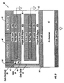
- Figure 1 is a cross-sectional side view of a vertical n-channel (i.e., NMOS) HVFET 20 in accordance with one embodiment of the present invention. It should be understood that the elements in the figures are representational, and are not drawn to scale in the interest of clarity. It is also appreciated that a p-channel transistor may be realized by utilizing the opposite conductivity types for all of the illustrated diffusion/doped regions. Furthermore, although the figure appears to show two separate devices, those of skill will understand that such transistor structures are commonly fabricated in an annular, interdigitated, or otherwise replicated manner.
- NMOS n-channel
- the device structure of Figure 1 includes an insulated-gate, field-effect transistor (IGFET) having a gate 30 (comprised, for example, of polysilicon), and a gate-insulating layer 29 that insulates gate 30 from the underlying semiconductor regions.
- Gate-insulating layer 29 may comprise ordinary silicon dioxide or another appropriate dielectric insulating material.
- the extended drain region of vertical HVFET 20 comprises two or more parallel N-type drift regions 22 situated between p-type body regions 26 and extending down to the N+ substrate 21.
- Figure 1 shows drift region 22a extending from beneath gate oxide 29a between P-body regions 26a & 26b down to N+ substrate 21.
- drift region 22b extends from gate oxide 29b between P-body regions 26c & 26d down to N+ substrate 21.
- Source electrode 32 is electrically connected to N+ source regions 27, which are disposed in respective P-body regions 26.
- N+ source region 27a is disposed in P-body region 26a;
- N+ region 27b is disposed in P-body region 27b, and so on.
- the area of the P-body regions directly beneath gate 30 (between N+ source regions 27 and drift regions 22) comprises the IGFET channel region of the transistor.
- the gate region is a metal-oxide semiconductor (MOS), and the IGFET is a NMOS transistor.
- MOS metal-oxide semiconductor
- the IGFET is a NMOS transistor.
- the channel regions of HVFET 20 are defined at one end by N+ source regions 27 and at the other end by N-type drift regions 22, which extend vertically from gate oxide 29 down to the N+ substrate 21. Insulating layers 33 separate gate 30 from source electrode 32.
- n-type extended drain or drift regions 22 are separated laterally by insulating regions or dielectric layers 28.
- dielectric layers 28 extend vertically from beneath P-body regions 26 down to N+ substrate 21 along the full vertical length of the drift regions 22.
- dielectric layers 28 may comprise silicon dioxide, but other insulating materials, such as silicon nitride, may also be used.
- Field plate members 24 Disposed within each of the dielectric layers 28, and fully insulated from the semiconductor substrate 21 and drift regions 22, is a field plate member 24.
- Field plate members 24 comprise a conducting layer of material such as heavily doped polysilicon, metal, metal alloys, etc.
- each of the field plate members 24 is electrically connected to source electrode 32.
- the field plate members may be connected to a separate electrode.
- Gates 30 are also connected to a separate electrode (not shown). Drain electrode 31 provides electrical connection to the bottom of N+ substrate 21.
- the extended drain region of vertical NMOS high-voltage transistor 20 of Figure 1 consists of a plurality of laterally interleaved layers of doped semiconductor material (e.g., n-type), insulating material (e.g., silicon dioxide), and conducting material (e.g., heavily-doped polysilicon).
- doped semiconductor material e.g., n-type
- insulating material e.g., silicon dioxide
- conducting material e.g., heavily-doped polysilicon
- the N-type drift region is normally very thick (i.e., long) and lightly doped; both of which contribute to high on state resistance.
- the doping in the N-type drift regions may be considerably higher, such that the on-state resistance is dramatically lowered. Lowering the on-state resistance is achieved in HVFET 20 by the use of multiple, parallel-arranged extended drain or drift regions.
- a high voltage e.g., 200V-1200V
- the doping profile in the drift regions 22 is tailored such that the resulting electric field is approximately constant along the path from the drain to the source.
- the doping concentration may be highest near the N+ substrate 21, lowest the near the P-body regions 26, and linearly graded in between.
- both the N-type drift regions 22 and oxide layers 28 should be designed so as to guard against prevent premature avalanche breakdown.
- Avalanche breakdown can be avoided by making the drift region relatively narrow, which reduces the ionization path and thereby increases the critical electric field at which avalanche occurs.
- making oxide layers 28 relatively wide allows the device structure to support a larger voltage for a given electric field.
- a device manufactured in accordance with Figure 1 having a drift region that is about 50um high and about 0.4 - 0.8 um wide, with an oxide layer width in the approximate range of 3.0 - 4.0 um is capable of supporting about 800V.
- the doping in the drift region may be linearly graded from about 5 x 10 15 cm -3 near the P-body regions to about 1 x 10 17 cm -3 near the N+ substrate.
- the on-state resistance of such a device is about 1.0 ohm-mm 2 .
- HVFET 20 may be improved when manufactured as a smaller total cell pitch (i.e., combined width of field plate, oxide layer and drift regions) because the contribution of each drift region is fairly constant.
- HVFET 40 of Figure 2 operates according to the same principles discussed in connection with the transistor structure of Figure 1, except that current flows laterally, as opposed to vertically, through the drift regions. Note that in the embodiment of Figure 2, field plate members 44 are fully insulated from the semiconductor material by oxide layers 49.
- field plate member 44a is disposed within oxide layer 49a just below the source and drain electrodes 46 and 45, respectively.
- Field plate member 44b is disposed within oxide layer 49b below N-type drift region 42a and above N-type drift region 42b.
- the field plate members may be connected to a field plate electrode at a certain location out of the plane of the figure.
- the N-type drift region which comprises the extended drain of the transistor, extends laterally from beneath P-body region 48 across to N+ drain region 43.
- N+ drain region 43 connects both drift regions 42a & 42b with drain electrode 45.
- An N+ source region 47 which is electrically connected to source electrode 46, is disposed adjacent P-body region 48.
- the HVFET 40 utilizes a vertical MOS gate structure 12 that comprises a gate electrode 56 that connects to gate 55.
- gate 55 comprises a layer of polysilicon that extends vertically from gate electrode 56.
- Gate 55 extends below the P-body region, and may extend down to oxide layer 50, as shown.
- Gate 55 is insulated from N+ source region 47, P-body region 48, and N-type drift region 42 by gate oxide 53.
- An oxide region 58 separates gate electrode 56 from source electrode 46.
- Oxide layer 50 insulates N+ substrate 41 from gate 55, N-type drift region 42, and N+ drain region 43. As can be seen, oxide layer 50 extends laterally over N+ substrate 41 beneath each of the regions 42, 43, and 55. Substrate electrode 57 provides electrical connection to the bottom of N+ substrate 41. The substrate may serve as the bottom field plate for drift region 42b.
- HVFET 40 The on-state and off-state operations of HVFET 40 are similar to those described for the embodiment of Figure 1. In this case, however, the source and drain electrodes are located on the top surface. This means that electrons flows down through N+ source region 47, across the channel region formed in P-body region 48 adjacent to gate oxide 53, laterally across the N-type drift regions 42, and up through the N+ drain region 43 before reaching the drain electrode.
- Figure 2 shows a trench gate structure
- planar gate structures could also be used.
- a trench drain structure could also be used in an alternative implementation.
- the embodiment of Figure 2 shows the extended drain region comprising two laterally-extending, parallel N-type drift regions 42a and 42b, other embodiments may utilize more than two parallel drift regions.
- the embodiment of Figure 2 is not limited to just two drift regions, but could include any number of layers of drift, oxide, and field plate regions within manufacturing limits.
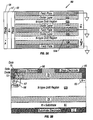
- Figures 3A & 3B illustrate another embodiment of a lateral HVFET in accordance with the present invention.
- Figure 3A is a top view of a lateral HVNMOS transistor 60
- Figure 3B is a cross-sectional side view of the same device, taken along cut lines A-A', which extends through drift region 62a.
- the source electrode 66, drain electrode 65, gate 75, gate oxide 73 and oxide layer 79 are not depicted in Figure 3A to avoid confusion. These elements are shown in the cross-sectional side view of Figure 3B.
- the lateral device structure of Figure 3 is similar to that shown in Figure 2. But rather than orient the drift, oxide, and field plate layered regions on top of one another (vertically), the embodiment of Figure 3 has these regions oriented side-by-side. Unlike the embodiment of Figure 2, each of the N-type drift regions 62, oxide layers 69, and field plate members 64 extend from underlying insulating layer 70 toward the upper substrate surface. Each of the N-type drift regions 62 and field plate members 64 are insulated from N+ substrate 61 by insulating layer 70. In one embodiment, layer 70 comprises silicon dioxide. An additional electrode 77 provides electrical connection to the bottom of N+ substrate 61.
- HVNMOS transistor 60 The planar gate and drain configurations of HVNMOS transistor 60 are illustrated in the side view of Figure 3B.
- a trench drain structure and/or a trench gate structure may be utilized.
- a gate member 75 is disposed above P-body region 68 and is insulated from the semiconductor substrate by a gate oxide 73.
- Source electrode 66 contacts N+ source region 67, which is disposed in P-body region 68.
- P-body region 68 is itself shown disposed in N-type drift region 62.
- N+ drain region 63 is disposed at the opposite end of the N-type drift region 62 and is electrically connected to drain electrode 65.
- the embodiments of Figures 2 and 3 show the field plate members being coupled to the lowest chip potential, e.g., ground.
- the source may be tied to the field plate members (at the lowest chip potential), or, alternatively, the source region may be left floating.
- the embodiments of Figures 1-3 are not limited to a source follower configuration.
- Each of the transistor structures of the present invention may be implemented as a four-terminal device, wherein the drain, source, field plate members, and insulated gate members are connected to a separate circuit terminal. In another embodiment, the field plate and insulated gate members may be connected together.
- transistor 80 comprises a plurality of parallel-arranged N-type drift regions 82 that extend vertically from P-body regions 86 down to the N+ substrate 81. Each of the drift regions 82 is adjoined on both sides by an oxide layer 88.
- N-type drift region 82a is bounded on one side by oxide layer 88a and on the opposite side by oxide layer 88b.
- a field plate member 84 Disposed within each of the oxide layers 88, and fully insulated from the drift region and substrate semiconductor materials, is a field plate member 84 that may be electrically connected to source electrode 92.
- the N-type drift regions 82, oxide layers 88, and field plate members 84 collectively comprise a parallel layered structure that extends in a lateral direction, which is perpendicular to the direction of current flow in the on-state.
- transistor 80 When transistor 80 is in the on-state, current flows vertically from the drain electrode 91 through the parallel N-type drift regions 82, through the MOS channel formed on the sidewalls of the P-body region, to the source electrode 92.
- the trench gate structure of vertical HVNMOS transistor 80 comprises gate members 90 disposed between field plate members 84 and P-body regions 86.
- a pair of N+ source regions 87 is disposed in each of P-body regions 86 on opposite sides.
- Each P-body region 86 is located at one end of a corresponding N-type drift region 82.
- a thin gate-insulating layer 89 e.g., oxide insulates each of gate members 90 (e.g., polysilicon) from the P-body semiconductor material.
- Figure 4 shows gate members 90a & 90b disposed along opposite sides of P-body region 86a.
- N+ source regions 87a & 87b are disposed in P-body region 86a at opposite sides adjacent to the gate members; both regions 87a & 87b are electrically connected to source electrode 92.
- P-body region 86a adjoins the source electrode at one end and drift region 82a at the other end.
- transistor 80 is in the on-state conducting channel regions are formed along the sides of P-body region 86a such that current flows from source electrode 92, through N+ regions 87, across P-body 86, down through N-type drift regions 82 and N+ substrate 81, to drain electrode 91.
- each P-body region 86 of Figure 4 may alternatively be replaced by a single N+ region that extends across the full width of region 86 adjacent to source electrode 92.
- the P-body region may be connected to the source electrode at various points (dimensionally into the page of the figure.)
- source electrode 92 may protrude through N+ source 87 to contact the underlying P-body region 86 (see Figure 5K).
- the trench gate structure of the embodiment of Figure 4 potentially offers an advantage of a simplified manufacturing process, due to the elimination of the T-shaped semiconductor regions shown in Figure 1. Also, the vertical HVNMOS structure of transistor 80 may provide lower on-resistance due to the elimination of the JFET structure formed between the P-body regions.
- Figures 5A-5K illustrate the various processing steps that may be employed to fabricate a vertical high-voltage transistor in accordance with the present invention.
- the described fabrication method may be used not only to form the device of Figure 5K, but also the vertical device structure shown in Figure 4.
- Figure 5A shows a vertical high-voltage transistor after the initial processing step of forming an epitaxial layer 101 of n-type semiconductor material on an N+ substrate 100.
- the device structure should have an epitaxial layer that is about 15um to 120um thick.
- the epitaxial layer of the device shown in Figure 5 is 40um thick.
- the N+ substrate 100 is heavily doped to minimize its resistance to current flowing through to the drain electrode, which is located on the bottom of the substrate in the completed device.
- Substrate 100 may be thinned, for example, by grinding or etching, and metal may be deposited on its bottom surface to further reduce the on-resistance of the transistor. Most often, these processing steps would be performed after the topside processing has been completed.
- the thickness and doping of epitaxial layer 101 largely determine the Vbd of the device.
- the doping may be carried out as the epitaxial layer is being formed.
- the optimal doping profile is linearly graded from the drain (at the bottom, adjacent to N+ substrate 100) to the source (at the top). Tailoring the doping concentration so that it is heavier near the substrate 100 results in a more uniform electric-field distribution. Linear grading may stop at some point below the top surface of the epitaxial layer 101.
- the doping concentration is approximately 2 x 10 15 cm -3 near the P-body region to about 6 x 10 16 cm -3 near the N+ substrate 100.
- FIG. 5B shows a cross-sectional view of the device structure following etching of epitaxial layer 101 and part of substrate 100. Note that the lateral width of the etched trenches is determined by the combined thickness of the dielectric and conductive refill layers, as described below.
- the lateral thickness (i.e., width) of the N-type drift region(s) is desired to make the lateral thickness (i.e., width) of the N-type drift region(s) as narrow as can be reliably manufactured in order to achieve a very high Vbd with a low Rsp.
- a larger lateral thickness is easier to manufacture, but the specific on-resistance of the device suffers with a larger lateral thickness since the current is required to flow across a larger silicon area.
- the thickness is in the approximate range of 0.4 to 1.2 microns. In this example, the thickness of the mesa is about 1um.
- Figure 5C shows the device structure of Figure 5B after partial filling of the etched trenches with a dielectric material, e.g., silicon dioxide.
- a dielectric material e.g., silicon dioxide.
- oxide region 102a covers one side of etched epitaxial region 101, while oxide region 102b covers the other side of epitaxial region 101.
- Oxide region 102 also covers the top surface of N+ substrate 100 in each of the trenches.
- the dielectric material may be introduced into the trenches using a variety of well-known methods. For instance, regions 102 may be grown thermally, deposited by chemical vapor deposition, and/or spun on in liquid form. For a given lateral thickness of epitaxial layer material 101, the thickness of the dielectric layer may be set to provide a required breakdown voltage, with thicker dielectric layers providing a higher Vbd. However, thicker dielectric layers increase the cell pitch of the transistor structure and result in higher specific on-resistance. In one implementation, the 600V device structure of Figure 5 has an oxide layer lateral thickness of 4um. For devices with other V bd performance, this thickness may be in the range of about 2um - 5um.
- Figure 5D illustrates the device structure of Figure 5C following the steps of filling the remaining portions of the trenches with a conductive material and planarizing the surface to form field plate regions 103.
- the conductive material may comprise a heavily doped polysilicon, a metal (or metal alloys), and/or silicide.
- Conductor regions 103a and 103b form the field plate members of the device.
- field plate members 103a and 103b should be made as narrow as can be reliably manufactured, since the field plate members occupy silicon area without directly contributing to device conductivity or breakdown voltage characteristics.
- the lateral thickness of field plate members 103 is approximately 0.5um - 1.0um.
- the planarization of the surface may be performed by conventional techniques such as chemical-mechanical polishing.
- fabrication of the extended drain region of the device is essentially complete.
- the remaining processing steps may be adapted to produce a stand-alone, high-voltage, depletion-mode MOSFET device structure (as shown in Figure 5G and Figure 6) or a high-voltage FET that incorporates a low-voltage MOSFET structure (e.g., Figure 5K), or other high-voltage devices.
- Figure 5E is a cross-sectional side view of the device structure of Figure 5D after the introduction of an N+ source region 105 at the top surface of epitaxial layer 101.
- Source region 105 may be formed using ordinary deposition, diffusion, and/or implantation processing techniques.
- interlevel dielectric layer 106 After formation of the N+ source region 105 an interlevel dielectric layer 106 if formed over the device.
- interlevel dielectric layer 106 comprises ordinary silicon dioxide that may be deposited and patterned by conventional methods. Openings are formed in dielectric layer 106 and a conductive layer of material (e.g., metal, silicide, etc.) is deposited and patterned to produce the structure shown in Figure 5F.
- source electrode 109 provides electrical connection to N+ source region 105
- electrodes 110a and 110b provide electrical connection to field plate members 103a and 103b, respectively.
- FIG. 5G shows the device structure of Figure 5F following formation of a drain electrode 111 on the bottom of N+ substrate 100.
- drain electrode 111 may be formed using the conventional technique of metal sputtering.
- the bottom of the substrate may first be subjected to grinding, implanting, etc., to lower the drain contact resistance.
- the device of Figure 5G represents a completed high-voltage transistor having a stand-alone drift region; that is, the device of Figure 5G does not include a low-voltage, series MOSFET structure at the top of the epitaxial layer. Instead, the extended drift region formed by the epitaxial layer, itself, performs the function of the MOSFET without the inclusion of a P-body region. Practitioners in the arts will note that in this device structure current cannot be completely turned-off, since there exists a continuous n-type path for electrons to flow from source electrode 109 to drain electrode 111. Current flow in the device structure of Figure 5G, however, does saturate when the mesa-like epitaxial layer 101 is pinched-off at high drain voltages.
- the device structure of Figure 6 achieves pinch-off of the extended drain region at lower voltages than the device of Figure 5G. This is achieved by reducing the spacing between the field plate members 103 and epitaxial layer 101 near the top of the N-type drift region, thereby increasing the capacitance to pinch-off the vertical drift region at a relatively low voltage.
- Figure 6 shows a multi-tiered field plate structure extending laterally into oxide regions 102a & 102b to control the pinch-off voltage and, therefore, the saturation current.
- the field plate members may comprise a single step, a linearly graded lateral extension, or some other profile shape designed to achieve the same result.
- FIG. 5H-5K there is shown an alternative processing sequence that may be used to fabricate a vertical HVNMOS transistor that includes an insulated gate MOS structure.
- Trenches 112a and 112b are formed in respective dielectric layers 102a and 102b on opposite sides of epitaxial layer 101 to accommodate the formation of the insulated gate structure.
- the depth of trenches 112a and 112b extends from the surface of N+ source region 105 to a depth governed by the intended MOSFET channel length and field plating considerations. In this example, the trench depth is about 1-5um.
- trenches 112 may be formed by appropriate application of a patterned masking layer to the semiconductor substrate followed by conventional dry or wet etching techniques into oxide layer 102.
- Figure 5J shows the device after formation of gate dielectric layers 116 and gate members 113 within trenches 112.
- the gate dielectric layers 116a & 116b may be formed by growing or depositing oxide on the sidewalls of the stacked N+ source, P-body, and epitaxial regions.
- the device threshold voltage determines the thickness of layers 116.
- layers 116 comprise silicon dioxide having a thickness on the order of 250 - 1000 angstroms.
- a portion of dielectric layers 112 isolates field plate members 103 from gate members 113.
- trenches 112 may expose the top portion of field plate 103 and the same processing steps used to create layers 116 may also be used to form dielectric layers on the sidewalls of the field plates to isolate the field plates from the gate members.
- a conductive material such as doped polysilicon, may be deposited to fill the remaining portions of the trenches.
- the doped polysilicon forms the gate members 113a and 113b of the MOS transistor structure.
- Figure 5J shows the device after introduction of a P-body region 107 and a N+ source region 105 at the top surface of epitaxial region 101. In the completed device, application of a sufficient voltage to gate members 113 causes a conductive channel to be formed along the sidewall portions of P-body region 107 between N+ source region 105 and epitaxial region 101.
- the channel length is therefore determined by the thickness of P-body region 107, which, for the particular embodiment shown, may be approximately 0.5um-3.0um, with the N+ source region 105 in the range of about 0.1-0.5um.
- a shorter channel length results in a lower channel resistance, which likewise reduces the on-resistance of the device. It should be understood, however, that a too short channel would cause punch-through problems.
- Figure 5K shows the completed HVFET device structure following formation of an interlevel dielectric layer 106 (e.g., silicon dioxide, silicon nitride, etc.).
- This layer may be deposited and patterned to form contact openings.
- the etching of layer 106 is followed by etching of the field plates, gate members, N+ and P-body regions.
- a conductive layer e.g., metal, silicide, etc.
- the optional etching step described above allows the source electrode to contact the P-body region without patterning the N+ source region, thus simplifying the process.
- a conductive layer may also be applied to the bottom of substrate 100 (after optional treatment by grinding, etching, implanting, etc.) to form the drain electrode 111.
- source electrode 109 is shown extending down to P-body 107 in the cross-sectional view of Figure 5K, in other embodiments electrode may only extend to the upper surface of source region 105. It should also be appreciated that electrode 109 does not separate region 105 into two separate source regions in the illustration of Figure 5K. Rather, electrode 109 is fabricated in the form of a plug that is surrounded by N+ material that comprises region 105.
- a method for fabricating a high-voltage transistor with an extended drain region comprises forming an epitaxial layer on a substrate, the epitaxial layer and the substrate being of a first conductivity type; then etching the epitaxial layer to form a pair of spaced-apart trenches that define first and second sidewall portions of the epitaxial layer. A dielectric layer is formed that partially fills each of the trenches, covering the first and second sidewall portions. The remaining portions of the trenches are then filled with a conductive material to form first and second field plate members that are insulated from the substrate and the epitaxial layer.
Priority Applications (4)
| Application Number | Priority Date | Filing Date | Title |
|---|---|---|---|
| EP10184810A EP2264747A3 (de) | 2001-09-07 | 2002-08-16 | Verfahren zur Herstellung eines Hochspannungstransistors |
| EP04078373A EP1536464A3 (de) | 2001-09-07 | 2002-08-16 | Verfahren zur Herstellung von Hochspannungshalbleiteranordnungen |
| EP10184815A EP2270843A3 (de) | 2001-09-07 | 2002-08-16 | Verfahren zur Herstellung eines Hochspannungstransistors mit isoliertem Gate |
| EP10184211A EP2264746A3 (de) | 2001-09-07 | 2002-08-16 | Verfahren zur Herstellung eines Hochspannungsfeldeffekttransistors |
Applications Claiming Priority (2)
| Application Number | Priority Date | Filing Date | Title |
|---|---|---|---|
| US09/948,879 US6635544B2 (en) | 2001-09-07 | 2001-09-07 | Method of fabricating a high-voltage transistor with a multi-layered extended drain structure |
| US948879 | 2001-09-07 |
Related Child Applications (1)
| Application Number | Title | Priority Date | Filing Date |
|---|---|---|---|
| EP04078373A Division EP1536464A3 (de) | 2001-09-07 | 2002-08-16 | Verfahren zur Herstellung von Hochspannungshalbleiteranordnungen |
Publications (2)
| Publication Number | Publication Date |
|---|---|
| EP1291907A2 true EP1291907A2 (de) | 2003-03-12 |
| EP1291907A3 EP1291907A3 (de) | 2004-02-04 |
Family
ID=25488349
Family Applications (5)
| Application Number | Title | Priority Date | Filing Date |
|---|---|---|---|
| EP04078373A Ceased EP1536464A3 (de) | 2001-09-07 | 2002-08-16 | Verfahren zur Herstellung von Hochspannungshalbleiteranordnungen |
| EP10184211A Withdrawn EP2264746A3 (de) | 2001-09-07 | 2002-08-16 | Verfahren zur Herstellung eines Hochspannungsfeldeffekttransistors |
| EP10184815A Withdrawn EP2270843A3 (de) | 2001-09-07 | 2002-08-16 | Verfahren zur Herstellung eines Hochspannungstransistors mit isoliertem Gate |
| EP02255737A Withdrawn EP1291907A3 (de) | 2001-09-07 | 2002-08-16 | Verfahren zur Herstellung von Hochspannungshalbleiteranordnungen |
| EP10184810A Withdrawn EP2264747A3 (de) | 2001-09-07 | 2002-08-16 | Verfahren zur Herstellung eines Hochspannungstransistors |
Family Applications Before (3)
| Application Number | Title | Priority Date | Filing Date |
|---|---|---|---|
| EP04078373A Ceased EP1536464A3 (de) | 2001-09-07 | 2002-08-16 | Verfahren zur Herstellung von Hochspannungshalbleiteranordnungen |
| EP10184211A Withdrawn EP2264746A3 (de) | 2001-09-07 | 2002-08-16 | Verfahren zur Herstellung eines Hochspannungsfeldeffekttransistors |
| EP10184815A Withdrawn EP2270843A3 (de) | 2001-09-07 | 2002-08-16 | Verfahren zur Herstellung eines Hochspannungstransistors mit isoliertem Gate |
Family Applications After (1)
| Application Number | Title | Priority Date | Filing Date |
|---|---|---|---|
| EP10184810A Withdrawn EP2264747A3 (de) | 2001-09-07 | 2002-08-16 | Verfahren zur Herstellung eines Hochspannungstransistors |
Country Status (3)
| Country | Link |
|---|---|
| US (8) | US6635544B2 (de) |
| EP (5) | EP1536464A3 (de) |
| JP (3) | JP4284428B2 (de) |
Cited By (9)
| Publication number | Priority date | Publication date | Assignee | Title |
|---|---|---|---|---|
| WO2005091339A2 (en) * | 2004-03-19 | 2005-09-29 | Hewlett-Packard Development Company, L.P. | Method of fabricating a semiconductor structure |
| DE10313712B4 (de) * | 2003-03-27 | 2008-04-03 | Infineon Technologies Ag | Laterales mittels Feldeffekt steuerbares Halbleiterbauelement für HF-Anwendungen |
| EP1903417A3 (de) * | 2003-05-27 | 2009-01-21 | Power Integrations, Inc. | Steuerungselement für eine elektronische Schaltung mit Auslaufelement |
| US8120097B2 (en) | 2004-07-08 | 2012-02-21 | Power Integrations, Inc. | Method and apparatus for controlling a circuit with a high voltage sense device |
| DE102005052734B4 (de) * | 2005-10-06 | 2012-02-23 | Infineon Technologies Ag | Halbleiterstruktur, Verfahren zum Betreiben einer Halbleiterstruktur und Verfahren zum Herstellen einer Halbleiterstruktur |
| US9537001B2 (en) | 2014-07-30 | 2017-01-03 | Fairchild Semiconductor Corporation | Reduction of degradation due to hot carrier injection |
| CN106328718A (zh) * | 2016-11-04 | 2017-01-11 | 四川洪芯微科技有限公司 | 一种台面二极管 |
| DE102016104757A1 (de) * | 2016-03-15 | 2017-09-21 | Infineon Technologies Austria Ag | Halbleitertransistor und Verfahren zum Bilden des Halbleitertransistors |
| CN113690301A (zh) * | 2020-05-18 | 2021-11-23 | 华润微电子(重庆)有限公司 | 半导体器件及其制备方法 |
Families Citing this family (92)
| Publication number | Priority date | Publication date | Assignee | Title |
|---|---|---|---|---|
| US6818513B2 (en) | 2001-01-30 | 2004-11-16 | Fairchild Semiconductor Corporation | Method of forming a field effect transistor having a lateral depletion structure |
| US7221011B2 (en) | 2001-09-07 | 2007-05-22 | Power Integrations, Inc. | High-voltage vertical transistor with a multi-gradient drain doping profile |
| US6573558B2 (en) * | 2001-09-07 | 2003-06-03 | Power Integrations, Inc. | High-voltage vertical transistor with a multi-layered extended drain structure |
| US6635544B2 (en) * | 2001-09-07 | 2003-10-21 | Power Intergrations, Inc. | Method of fabricating a high-voltage transistor with a multi-layered extended drain structure |
| US7786533B2 (en) * | 2001-09-07 | 2010-08-31 | Power Integrations, Inc. | High-voltage vertical transistor with edge termination structure |
| US6555873B2 (en) | 2001-09-07 | 2003-04-29 | Power Integrations, Inc. | High-voltage lateral transistor with a multi-layered extended drain structure |
| US6916398B2 (en) | 2001-10-26 | 2005-07-12 | Applied Materials, Inc. | Gas delivery apparatus and method for atomic layer deposition |
| DE10161125C1 (de) * | 2001-12-12 | 2003-07-31 | Infineon Technologies Ag | Halbleiterbauelement mit optimierter Stromdichte |
| US7400014B2 (en) | 2004-04-20 | 2008-07-15 | International Rectifier Corporation | ACCUFET with schottky source contact |
| US7482654B2 (en) * | 2004-04-20 | 2009-01-27 | International Rectifier Corporation | MOSgated power semiconductor device with source field electrode |
| US7183610B2 (en) * | 2004-04-30 | 2007-02-27 | Siliconix Incorporated | Super trench MOSFET including buried source electrode and method of fabricating the same |
| DE102004063946B4 (de) | 2004-05-19 | 2018-03-22 | Infineon Technologies Ag | Transistoranordnungen mit einer in einem Trennungstrench angeordneten Elektrode |
| US7268395B2 (en) | 2004-06-04 | 2007-09-11 | International Rectifier Corporation | Deep trench super switch device |
| JP2008504697A (ja) * | 2004-06-25 | 2008-02-14 | インターナショナル レクティファイアー コーポレイション | ソースフィールド電極を有するmosゲートが設けられているパワー半導体デバイス |
| US7087959B2 (en) * | 2004-08-18 | 2006-08-08 | Agere Systems Inc. | Metal-oxide-semiconductor device having an enhanced shielding structure |
| US7135748B2 (en) * | 2004-10-26 | 2006-11-14 | Power Integrations, Inc. | Integrated circuit with multi-length output transistor segment |
| JP4984398B2 (ja) * | 2005-02-04 | 2012-07-25 | 富士電機株式会社 | 半導体装置およびその製造方法 |
| DE102005014743B4 (de) * | 2005-03-31 | 2013-12-05 | Infineon Technologies Austria Ag | MOS-Feldplattentrench-Transistoreinrichtung |
| GB0508407D0 (en) * | 2005-04-26 | 2005-06-01 | Ami Semiconductor Belgium Bvba | Alignment of trench for MOS |
| US20060255401A1 (en) * | 2005-05-11 | 2006-11-16 | Yang Robert K | Increasing breakdown voltage in semiconductor devices with vertical series capacitive structures |
| US20070012983A1 (en) * | 2005-07-15 | 2007-01-18 | Yang Robert K | Terminations for semiconductor devices with floating vertical series capacitive structures |
| JP5070751B2 (ja) * | 2006-01-31 | 2012-11-14 | 富士電機株式会社 | 半導体装置およびその製造方法 |
| US7554153B2 (en) * | 2006-03-07 | 2009-06-30 | International Rectifier Corporation | Power semiconductor device |
| US7381618B2 (en) * | 2006-10-03 | 2008-06-03 | Power Integrations, Inc. | Gate etch process for a high-voltage FET |
| US8093621B2 (en) | 2008-12-23 | 2012-01-10 | Power Integrations, Inc. | VTS insulated gate bipolar transistor |
| JP4601603B2 (ja) * | 2006-12-27 | 2010-12-22 | ルネサスエレクトロニクス株式会社 | パワーmisfet、半導体装置およびdc/dcコンバータ |
| JP5298432B2 (ja) * | 2007-01-31 | 2013-09-25 | 富士電機株式会社 | 半導体装置およびその製造方法 |
| US7557406B2 (en) * | 2007-02-16 | 2009-07-07 | Power Integrations, Inc. | Segmented pillar layout for a high-voltage vertical transistor |
| US7859037B2 (en) | 2007-02-16 | 2010-12-28 | Power Integrations, Inc. | Checkerboarded high-voltage vertical transistor layout |
| US7468536B2 (en) | 2007-02-16 | 2008-12-23 | Power Integrations, Inc. | Gate metal routing for transistor with checkerboarded layout |
| US8653583B2 (en) | 2007-02-16 | 2014-02-18 | Power Integrations, Inc. | Sensing FET integrated with a high-voltage transistor |
| US7595523B2 (en) | 2007-02-16 | 2009-09-29 | Power Integrations, Inc. | Gate pullback at ends of high-voltage vertical transistor structure |
| US8159024B2 (en) * | 2007-04-20 | 2012-04-17 | Rensselaer Polytechnic Institute | High voltage (>100V) lateral trench power MOSFET with low specific-on-resistance |
| US7875962B2 (en) * | 2007-10-15 | 2011-01-25 | Power Integrations, Inc. | Package for a power semiconductor device |
| US8129815B2 (en) | 2009-08-20 | 2012-03-06 | Power Integrations, Inc | High-voltage transistor device with integrated resistor |
| US7816759B2 (en) * | 2008-01-09 | 2010-10-19 | Infineon Technologies Ag | Integrated circuit including isolation regions substantially through substrate |
| US7772651B2 (en) * | 2008-01-11 | 2010-08-10 | International Business Machines Corporation | Semiconductor-on-insulator high-voltage device structures, methods of fabricating such device structures, and design structures for high-voltage circuits |
| US7786535B2 (en) * | 2008-01-11 | 2010-08-31 | International Business Machines Corporation | Design structures for high-voltage integrated circuits |
| US7790524B2 (en) * | 2008-01-11 | 2010-09-07 | International Business Machines Corporation | Device and design structures for memory cells in a non-volatile random access memory and methods of fabricating such device structures |
| US7790543B2 (en) * | 2008-01-11 | 2010-09-07 | International Business Machines Corporation | Device structures for a metal-oxide-semiconductor field effect transistor and methods of fabricating such device structures |
| WO2009110229A1 (ja) * | 2008-03-07 | 2009-09-11 | 三菱電機株式会社 | 炭化珪素半導体装置およびその製造方法 |
| US7700428B2 (en) * | 2008-05-09 | 2010-04-20 | International Business Machines Corporation | Methods of fabricating a device structure for use as a memory cell in a non-volatile random access memory |
| US7804124B2 (en) * | 2008-05-09 | 2010-09-28 | International Business Machines Corporation | Device structures for a memory cell of a non-volatile random access memory and design structures for a non-volatile random access memory |
| US7671408B2 (en) * | 2008-07-09 | 2010-03-02 | Texas Instruments Incorporated | Vertical drain extended MOSFET transistor with vertical trench field plate |
| TWI385802B (zh) * | 2008-09-08 | 2013-02-11 | Niko Semiconductor Co Ltd | 高壓金氧半導體元件及其製作方法 |
| US7964912B2 (en) | 2008-09-18 | 2011-06-21 | Power Integrations, Inc. | High-voltage vertical transistor with a varied width silicon pillar |
| US8044459B2 (en) | 2008-11-10 | 2011-10-25 | Infineon Technologies Austria Ag | Semiconductor device with trench field plate including first and second semiconductor materials |
| US7871882B2 (en) | 2008-12-20 | 2011-01-18 | Power Integrations, Inc. | Method of fabricating a deep trench insulated gate bipolar transistor |
| US20100155831A1 (en) * | 2008-12-20 | 2010-06-24 | Power Integrations, Inc. | Deep trench insulated gate bipolar transistor |
| CA2762763A1 (en) | 2009-06-19 | 2010-12-23 | Ss Sc Ip, Llc | Vertical junction field effect transistors and diodes having graded doped regions and methods of making |
| US8207455B2 (en) * | 2009-07-31 | 2012-06-26 | Power Integrations, Inc. | Power semiconductor package with bottom surface protrusions |
| US8115457B2 (en) | 2009-07-31 | 2012-02-14 | Power Integrations, Inc. | Method and apparatus for implementing a power converter input terminal voltage discharge circuit |
| US8207577B2 (en) * | 2009-09-29 | 2012-06-26 | Power Integrations, Inc. | High-voltage transistor structure with reduced gate capacitance |
| US7893754B1 (en) | 2009-10-02 | 2011-02-22 | Power Integrations, Inc. | Temperature independent reference circuit |
| US8634218B2 (en) * | 2009-10-06 | 2014-01-21 | Power Integrations, Inc. | Monolithic AC/DC converter for generating DC supply voltage |
| JP5452195B2 (ja) | 2009-12-03 | 2014-03-26 | 株式会社 日立パワーデバイス | 半導体装置及びそれを用いた電力変換装置 |
| US8310845B2 (en) * | 2010-02-10 | 2012-11-13 | Power Integrations, Inc. | Power supply circuit with a control terminal for different functional modes of operation |
| US8305826B2 (en) | 2010-05-07 | 2012-11-06 | Power Integrations, Inc. | Method and apparatus for programming an anti-fuse element in a high-voltage integrated circuit |
| US8164125B2 (en) | 2010-05-07 | 2012-04-24 | Power Integrations, Inc. | Integrated transistor and anti-fuse as programming element for a high-voltage integrated circuit |
| US7932738B1 (en) | 2010-05-07 | 2011-04-26 | Power Integrations, Inc. | Method and apparatus for reading a programmable anti-fuse element in a high-voltage integrated circuit |
| CN102254796B (zh) * | 2010-05-20 | 2014-05-21 | 上海华虹宏力半导体制造有限公司 | 形成交替排列的p型和n型半导体薄层的方法 |
| US8497203B2 (en) | 2010-08-13 | 2013-07-30 | International Business Machines Corporation | Semiconductor structures and methods of manufacture |
| US7977742B1 (en) | 2010-08-20 | 2011-07-12 | Monolithic Power Systems, Inc. | Trench-gate MOSFET with capacitively depleted drift region |
| US8313995B2 (en) * | 2011-01-13 | 2012-11-20 | Infineon Technologies Austria Ag | Method for manufacturing a semiconductor device |
| CN102184944B (zh) * | 2011-04-29 | 2013-01-02 | 南京邮电大学 | 一种横向功率器件的结终端结构 |
| US8643135B2 (en) * | 2011-05-31 | 2014-02-04 | Alpha And Omega Semiconductor Incorporated | Edge termination configurations for high voltage semiconductor power devices |
| US8803225B2 (en) * | 2012-01-12 | 2014-08-12 | Tsinghua University | Tunneling field effect transistor having a lightly doped buried layer |
| US8723178B2 (en) | 2012-01-20 | 2014-05-13 | Monolithic Power Systems, Inc. | Integrated field effect transistors with high voltage drain sensing |
| JP5461599B2 (ja) * | 2012-02-15 | 2014-04-02 | 三菱電機株式会社 | 電力用半導体装置 |
| US8941188B2 (en) * | 2012-03-26 | 2015-01-27 | Infineon Technologies Austria Ag | Semiconductor arrangement with a superjunction transistor and a further device integrated in a common semiconductor body |
| US8653600B2 (en) | 2012-06-01 | 2014-02-18 | Power Integrations, Inc. | High-voltage monolithic schottky device structure |
| JP5609950B2 (ja) * | 2012-11-12 | 2014-10-22 | 富士電機株式会社 | 半導体装置およびその製造方法 |
| US9455621B2 (en) | 2013-08-28 | 2016-09-27 | Power Integrations, Inc. | Controller IC with zero-crossing detector and capacitor discharge switching element |
| US9111766B2 (en) * | 2013-09-24 | 2015-08-18 | Infineon Technologies Austria Ag | Transistor device with a field electrode |
| US20150118810A1 (en) * | 2013-10-24 | 2015-04-30 | Madhur Bobde | Buried field ring field effect transistor (buf-fet) integrated with cells implanted with hole supply path |
| AU2014346844B2 (en) | 2013-11-06 | 2017-06-15 | Watt Fuel Cell Corp. | Chemical reactor with manifold for management of a flow of gaseous reaction medium thereto |
| US9543396B2 (en) | 2013-12-13 | 2017-01-10 | Power Integrations, Inc. | Vertical transistor device structure with cylindrically-shaped regions |
| US10325988B2 (en) | 2013-12-13 | 2019-06-18 | Power Integrations, Inc. | Vertical transistor device structure with cylindrically-shaped field plates |
| CN106463508A (zh) | 2014-04-01 | 2017-02-22 | 英派尔科技开发有限公司 | 具有闪络保护的垂直晶体管 |
| US9406750B2 (en) | 2014-11-19 | 2016-08-02 | Empire Technology Development Llc | Output capacitance reduction in power transistors |
| JP2016171268A (ja) | 2015-03-16 | 2016-09-23 | 株式会社東芝 | 半導体装置 |
| US9667154B2 (en) | 2015-09-18 | 2017-05-30 | Power Integrations, Inc. | Demand-controlled, low standby power linear shunt regulator |
| US9602009B1 (en) | 2015-12-08 | 2017-03-21 | Power Integrations, Inc. | Low voltage, closed loop controlled energy storage circuit |
| US9629218B1 (en) | 2015-12-28 | 2017-04-18 | Power Integrations, Inc. | Thermal protection for LED bleeder in fault condition |
| US10205024B2 (en) * | 2016-02-05 | 2019-02-12 | Taiwan Semiconductor Manufacturing Company Ltd. | Semiconductor structure having field plate and associated fabricating method |
| EP3440696B1 (de) | 2016-04-08 | 2021-06-09 | Power Integrations, Inc. | Integrierter widerstand für halbleiterbauelement |
| US9786784B1 (en) | 2016-05-27 | 2017-10-10 | Samsung Electronics Co., Ltd. | Vertical field effect transistor and method of fabricating the same |
| US10135357B1 (en) | 2017-09-07 | 2018-11-20 | Power Integrations, Inc. | Threshold detection with tap |
| CN111133586B (zh) * | 2017-10-05 | 2023-04-07 | 三菱电机株式会社 | 半导体装置 |
| CN109346524B (zh) * | 2018-09-30 | 2020-06-02 | 重庆大学 | 一种具有阶梯浓度多晶硅侧墙结构的超结vdmos器件 |
| EP3905335A1 (de) * | 2020-04-28 | 2021-11-03 | Infineon Technologies AG | Gruppe-iii-nitrid-basierte transistorvorrichtung |
| CN115050816B (zh) * | 2022-08-12 | 2022-10-21 | 无锡新洁能股份有限公司 | 一种高速平面栅功率器件及其制造方法 |
Citations (15)
| Publication number | Priority date | Publication date | Assignee | Title |
|---|---|---|---|---|
| US4754310A (en) | 1980-12-10 | 1988-06-28 | U.S. Philips Corp. | High voltage semiconductor device |
| US4811075A (en) | 1987-04-24 | 1989-03-07 | Power Integrations, Inc. | High voltage MOS transistors |
| US5126807A (en) * | 1990-06-13 | 1992-06-30 | Kabushiki Kaisha Toshiba | Vertical MOS transistor and its production method |
| US5438215A (en) | 1993-03-25 | 1995-08-01 | Siemens Aktiengesellschaft | Power MOSFET |
| US5637898A (en) | 1995-12-22 | 1997-06-10 | North Carolina State University | Vertical field effect transistors having improved breakdown voltage capability and low on-state resistance |
| WO1999034449A2 (en) | 1997-12-24 | 1999-07-08 | Koninklijke Philips Electronics N.V. | A high voltage thin film transistor with improved on-state characteristics and method for making same |
| US5973360A (en) | 1996-03-20 | 1999-10-26 | Siemens Aktiengesellschaft | Field effect-controllable semiconductor component |
| US5998833A (en) | 1998-10-26 | 1999-12-07 | North Carolina State University | Power semiconductor devices having improved high frequency switching and breakdown characteristics |
| US6075259A (en) | 1994-11-14 | 2000-06-13 | North Carolina State University | Power semiconductor devices that utilize buried insulating regions to achieve higher than parallel-plane breakdown voltages |
| DE19905421A1 (de) | 1999-02-10 | 2000-08-24 | Semikron Elektronik Gmbh | Leistungshalbleiterbauelement mit reduzierter Millerkapazität |
| JP2000349288A (ja) | 1999-06-09 | 2000-12-15 | Fuji Electric Co Ltd | 縦型mosfet |
| US6184555B1 (en) | 1996-02-05 | 2001-02-06 | Siemens Aktiengesellschaft | Field effect-controlled semiconductor component |
| US6191447B1 (en) | 1999-05-28 | 2001-02-20 | Micro-Ohm Corporation | Power semiconductor devices that utilize tapered trench-based insulating regions to improve electric field profiles in highly doped drift region mesas and methods of forming same |
| JP2001085688A (ja) | 1999-09-14 | 2001-03-30 | Toshiba Corp | 半導体装置及びその製造方法 |
| US6362505B1 (en) | 1998-11-27 | 2002-03-26 | Siemens Aktiengesellschaft | MOS field-effect transistor with auxiliary electrode |
Family Cites Families (171)
| Publication number | Priority date | Publication date | Assignee | Title |
|---|---|---|---|---|
| JPS5638867A (en) | 1979-09-07 | 1981-04-14 | Hitachi Ltd | Insulated gate type field effect transistor |
| US4343015A (en) * | 1980-05-14 | 1982-08-03 | General Electric Company | Vertical channel field effect transistor |
| JPS5712557A (en) | 1980-06-25 | 1982-01-22 | Sanyo Electric Co Ltd | High dielectric resisting mos transistor |
| JPS5710975A (en) | 1980-06-25 | 1982-01-20 | Sanyo Electric Co Ltd | High dielectric strength high transistor |
| JPS5712558A (en) | 1980-06-25 | 1982-01-22 | Sanyo Electric Co Ltd | Mos transistor having high withstand voltage |
| US4626879A (en) | 1982-12-21 | 1986-12-02 | North American Philips Corporation | Lateral double-diffused MOS transistor devices suitable for source-follower applications |
| US4738936A (en) * | 1983-07-01 | 1988-04-19 | Acrian, Inc. | Method of fabrication lateral FET structure having a substrate to source contact |
| US4626789A (en) | 1983-08-19 | 1986-12-02 | Hitachi, Ltd. | Demodulating circuit for data signal |
| JPS6064471A (ja) | 1983-09-19 | 1985-04-13 | Nec Corp | 高電圧絶縁ゲ−ト型電界効果トランジスタ |
| US4531173A (en) | 1983-11-02 | 1985-07-23 | Motorola, Inc. | Protective power foldback circuit for a power semiconductor |
| US4618541A (en) | 1984-12-21 | 1986-10-21 | Advanced Micro Devices, Inc. | Method of forming a silicon nitride film transparent to ultraviolet radiation and resulting article |
| JPS61168253A (ja) * | 1985-01-19 | 1986-07-29 | Sharp Corp | 高耐圧mos電界効果半導体装置 |
| US4665426A (en) | 1985-02-01 | 1987-05-12 | Advanced Micro Devices, Inc. | EPROM with ultraviolet radiation transparent silicon nitride passivation layer |
| US4667173A (en) * | 1985-08-29 | 1987-05-19 | Kabushiki Kaisha Toshiba | Line filter |
| US4963951A (en) | 1985-11-29 | 1990-10-16 | General Electric Company | Lateral insulated gate bipolar transistors with improved latch-up immunity |
| US4764800A (en) | 1986-05-07 | 1988-08-16 | Advanced Micro Devices, Inc. | Seal structure for an integrated circuit |
| US4769685A (en) | 1986-10-27 | 1988-09-06 | General Motors Corporation | Recessed-gate junction-MOS field effect transistor |
| US4796070A (en) * | 1987-01-15 | 1989-01-03 | General Electric Company | Lateral charge control semiconductor device and method of fabrication |
| US5010024A (en) | 1987-03-04 | 1991-04-23 | Advanced Micro Devices, Inc. | Passivation for integrated circuit structures |
| US4890144A (en) | 1987-09-14 | 1989-12-26 | Motorola, Inc. | Integrated circuit trench cell |
| US5362711A (en) * | 1987-09-21 | 1994-11-08 | Kanegafuchi Chemical Industry Co., Ltd. | Method for producing single crystal superconducting LnA2 Cu3 O7-x films |
| EP0308612B1 (de) | 1987-09-24 | 1994-10-12 | Mitsubishi Denki Kabushiki Kaisha | Feldeffekttransistor und dessen Herstellungsmethode |
| JPH0734471B2 (ja) * | 1987-09-24 | 1995-04-12 | 三菱電機株式会社 | 電界効果型半導体装置 |
| JPH01112764A (ja) | 1987-10-27 | 1989-05-01 | Nec Corp | 半導体装置 |
| US4939566A (en) | 1987-10-30 | 1990-07-03 | North American Philips Corporation | Semiconductor switch with parallel DMOS and IGT |
| US4926074A (en) | 1987-10-30 | 1990-05-15 | North American Philips Corporation | Semiconductor switch with parallel lateral double diffused MOS transistor and lateral insulated gate transistor |
| US4890146A (en) | 1987-12-16 | 1989-12-26 | Siliconix Incorporated | High voltage level shift semiconductor device |
| US4922327A (en) | 1987-12-24 | 1990-05-01 | University Of Toronto Innovations Foundation | Semiconductor LDMOS device with upper and lower passages |
| DE68927866T2 (de) | 1988-01-14 | 1997-09-04 | Toshiba Kawasaki Kk | Methode zur Wertbestimmung für Leitungsfilter und zugehörige Komponenten |
| US4929987A (en) | 1988-02-01 | 1990-05-29 | General Instrument Corporation | Method for setting the threshold voltage of a power mosfet |
| US5025296A (en) | 1988-02-29 | 1991-06-18 | Motorola, Inc. | Center tapped FET |
| US5283201A (en) * | 1988-05-17 | 1994-02-01 | Advanced Power Technology, Inc. | High density power device fabrication process |
| JPH0775260B2 (ja) | 1988-06-01 | 1995-08-09 | 株式会社日立製作所 | 半導体装置 |
| US5237193A (en) * | 1988-06-24 | 1993-08-17 | Siliconix Incorporated | Lightly doped drain MOSFET with reduced on-resistance |
| EP0371785B1 (de) | 1988-11-29 | 1996-05-01 | Kabushiki Kaisha Toshiba | Lateraler Leitfähigkeitsmodulations-MOSFET |
| US5072266A (en) * | 1988-12-27 | 1991-12-10 | Siliconix Incorporated | Trench DMOS power transistor with field-shaping body profile and three-dimensional geometry |
| US5179362A (en) * | 1989-12-15 | 1993-01-12 | Kabushiki Kaisha Toshiba | Power line filter |
| US5008794A (en) | 1989-12-21 | 1991-04-16 | Power Integrations, Inc. | Regulated flyback converter with spike suppressing coupled inductors |
| JP2877408B2 (ja) | 1990-01-12 | 1999-03-31 | 株式会社東芝 | 導電変調型mosfet |
| JP2597412B2 (ja) | 1990-03-20 | 1997-04-09 | 三菱電機株式会社 | 半導体装置およびその製造方法 |
| US5040045A (en) | 1990-05-17 | 1991-08-13 | U.S. Philips Corporation | High voltage MOS transistor having shielded crossover path for a high voltage connection bus |
| US5242845A (en) * | 1990-06-13 | 1993-09-07 | Kabushiki Kaisha Toshiba | Method of production of vertical MOS transistor |
| JP2991753B2 (ja) | 1990-08-27 | 1999-12-20 | 松下電子工業株式会社 | 半導体装置及びその製造方法 |
| JP2599493B2 (ja) | 1990-08-27 | 1997-04-09 | 松下電子工業株式会社 | 半導体装置 |
| US5072268A (en) | 1991-03-12 | 1991-12-10 | Power Integrations, Inc. | MOS gated bipolar transistor |
| US5122848A (en) * | 1991-04-08 | 1992-06-16 | Micron Technology, Inc. | Insulated-gate vertical field-effect transistor with high current drive and minimum overlap capacitance |
| US5386136A (en) * | 1991-05-06 | 1995-01-31 | Siliconix Incorporated | Lightly-doped drain MOSFET with improved breakdown characteristics |
| US5146298A (en) | 1991-08-16 | 1992-09-08 | Eklund Klas H | Device which functions as a lateral double-diffused insulated gate field effect transistor or as a bipolar transistor |
| US5164891A (en) | 1991-08-21 | 1992-11-17 | Power Integrations, Inc. | Low noise voltage regulator and method using a gated single ended oscillator |
| US5258636A (en) | 1991-12-12 | 1993-11-02 | Power Integrations, Inc. | Narrow radius tips for high voltage semiconductor devices with interdigitated source and drain electrodes |
| US5270264A (en) | 1991-12-20 | 1993-12-14 | Intel Corporation | Process for filling submicron spaces with dielectric |
| US5744851A (en) * | 1992-01-27 | 1998-04-28 | Harris Corporation | Biasing of island-surrounding material to suppress reduction of breakdown voltage due to field plate acting on buried layer/island junction between high and low impurity concentration regions |
| US5285367A (en) | 1992-02-07 | 1994-02-08 | Power Integrations, Inc. | Linear load circuit to control switching power supplies under minimum load conditions |
| JP3435173B2 (ja) | 1992-07-10 | 2003-08-11 | 株式会社日立製作所 | 半導体装置 |
| US5294824A (en) * | 1992-07-31 | 1994-03-15 | Motorola, Inc. | High voltage transistor having reduced on-resistance |
| US5285369A (en) * | 1992-09-01 | 1994-02-08 | Power Integrations, Inc. | Switched mode power supply integrated circuit with start-up self-biasing |
| US5323044A (en) | 1992-10-02 | 1994-06-21 | Power Integrations, Inc. | Bi-directional MOSFET switch |
| DE4237110A1 (de) | 1992-11-03 | 1994-05-05 | Willi Waelte Elektronik Ingeni | Hydraulische Bremse für Fahrräder |
| US5326711A (en) * | 1993-01-04 | 1994-07-05 | Texas Instruments Incorporated | High performance high voltage vertical transistor and method of fabrication |
| JP3076468B2 (ja) | 1993-01-26 | 2000-08-14 | 松下電子工業株式会社 | 半導体装置 |
| US5274259A (en) | 1993-02-01 | 1993-12-28 | Power Integrations, Inc. | High voltage transistor |
| US5313082A (en) | 1993-02-16 | 1994-05-17 | Power Integrations, Inc. | High voltage MOS transistor with a low on-resistance |
| US5349225A (en) | 1993-04-12 | 1994-09-20 | Texas Instruments Incorporated | Field effect transistor with a lightly doped drain |
| JP3198200B2 (ja) * | 1993-04-30 | 2001-08-13 | 株式会社東芝 | 縦型mosトランジスタの製造方法 |
| US5324683A (en) | 1993-06-02 | 1994-06-28 | Motorola, Inc. | Method of forming a semiconductor structure having an air region |
| BE1007283A3 (nl) * | 1993-07-12 | 1995-05-09 | Philips Electronics Nv | Halfgeleiderinrichting met een most voorzien van een extended draingebied voor hoge spanningen. |
| ATE175523T1 (de) | 1993-09-17 | 1999-01-15 | Cons Ric Microelettronica | Eine integrierte vorrichtung mit einem bipolaren transistor und einem mosfet transistor in emittorschaltungsanordnung |
| US5523604A (en) | 1994-05-13 | 1996-06-04 | International Rectifier Corporation | Amorphous silicon layer for top surface of semiconductor device |
| CN1040814C (zh) | 1994-07-20 | 1998-11-18 | 电子科技大学 | 一种用于半导体器件的表面耐压区 |
| US5494853A (en) | 1994-07-25 | 1996-02-27 | United Microelectronics Corporation | Method to solve holes in passivation by metal layout |
| US5521105A (en) | 1994-08-12 | 1996-05-28 | United Microelectronics Corporation | Method of forming counter-doped island in power MOSFET |
| US5581100A (en) * | 1994-08-30 | 1996-12-03 | International Rectifier Corporation | Trench depletion MOSFET |
| US5550405A (en) | 1994-12-21 | 1996-08-27 | Advanced Micro Devices, Incorporated | Processing techniques for achieving production-worthy, low dielectric, low interconnect resistance and high performance ICS |
| US5656543A (en) | 1995-02-03 | 1997-08-12 | National Semiconductor Corporation | Fabrication of integrated circuits with borderless vias |
| DE69602114T2 (de) * | 1995-02-10 | 1999-08-19 | Siliconix Inc | Graben-Feldeffekttransistor mit PN-Verarmungsschicht-Barriere |
| JP3291958B2 (ja) | 1995-02-21 | 2002-06-17 | 富士電機株式会社 | バックソースmosfet |
| US5670828A (en) | 1995-02-21 | 1997-09-23 | Advanced Micro Devices, Inc. | Tunneling technology for reducing intra-conductive layer capacitance |
| US6140678A (en) * | 1995-06-02 | 2000-10-31 | Siliconix Incorporated | Trench-gated power MOSFET with protective diode |
| US5661322A (en) | 1995-06-02 | 1997-08-26 | Siliconix Incorporated | Bidirectional blocking accumulation-mode trench power MOSFET |
| US6049108A (en) | 1995-06-02 | 2000-04-11 | Siliconix Incorporated | Trench-gated MOSFET with bidirectional voltage clamping |
| US5659201A (en) | 1995-06-05 | 1997-08-19 | Advanced Micro Devices, Inc. | High conductivity interconnection line |
| KR100188096B1 (ko) | 1995-09-14 | 1999-06-01 | 김광호 | 반도체 장치 및 그 제조 방법 |
| US6097063A (en) | 1996-01-22 | 2000-08-01 | Fuji Electric Co., Ltd. | Semiconductor device having a plurality of parallel drift regions |
| JPH09266311A (ja) * | 1996-01-22 | 1997-10-07 | Fuji Electric Co Ltd | 半導体装置及びその製造方法 |
| DE69739206D1 (de) * | 1996-07-19 | 2009-02-26 | Siliconix Inc | Hochdichte-graben-dmos-transistor mit grabenbodemimplantierung |
| US5841166A (en) | 1996-09-10 | 1998-11-24 | Spectrian, Inc. | Lateral DMOS transistor for RF/microwave applications |
| US6800903B2 (en) | 1996-11-05 | 2004-10-05 | Power Integrations, Inc. | High-voltage transistor with multi-layer conduction region |
| US6207994B1 (en) | 1996-11-05 | 2001-03-27 | Power Integrations, Inc. | High-voltage transistor with multi-layer conduction region |
| US6168983B1 (en) | 1996-11-05 | 2001-01-02 | Power Integrations, Inc. | Method of making a high-voltage transistor with multiple lateral conduction layers |
| KR100228331B1 (ko) | 1996-12-30 | 1999-11-01 | 김영환 | 반도체 소자의 삼중웰 제조 방법 |
| JPH10256550A (ja) * | 1997-01-09 | 1998-09-25 | Toshiba Corp | 半導体装置 |
| DE69728852D1 (de) * | 1997-01-31 | 2004-06-03 | St Microelectronics Srl | Verfahren zur Herstellung von einer morphologischen Randstruktur um ein integriertes elektronisches Bauelement zu versiegeln, sowie ein entsprechendes Bauelement |
| JP3938964B2 (ja) * | 1997-02-10 | 2007-06-27 | 三菱電機株式会社 | 高耐圧半導体装置およびその製造方法 |
| JP3393544B2 (ja) | 1997-02-26 | 2003-04-07 | シャープ株式会社 | 半導体装置の製造方法 |
| US6133607A (en) * | 1997-05-22 | 2000-10-17 | Kabushiki Kaisha Toshiba | Semiconductor device |
| US5869875A (en) | 1997-06-10 | 1999-02-09 | Spectrian | Lateral diffused MOS transistor with trench source contact |
| US6054752A (en) * | 1997-06-30 | 2000-04-25 | Denso Corporation | Semiconductor device |
| JPH1197645A (ja) | 1997-09-19 | 1999-04-09 | Nec Corp | 半導体記憶装置 |
| US6194283B1 (en) * | 1997-10-29 | 2001-02-27 | Advanced Micro Devices, Inc. | High density trench fill due to new spacer fill method including isotropically etching silicon nitride spacers |
| US6316807B1 (en) * | 1997-12-05 | 2001-11-13 | Naoto Fujishima | Low on-resistance trench lateral MISFET with better switching characteristics and method for manufacturing same |
| US5988833A (en) | 1997-12-15 | 1999-11-23 | Ruud Lighting, Inc. | Adaptable directional floodlight |
| KR100429506B1 (ko) * | 1998-04-18 | 2004-11-20 | 삼성전자주식회사 | 통신시스템의 채널부호/복호장치 및 방법 |
| US6362064B2 (en) * | 1998-04-21 | 2002-03-26 | National Semiconductor Corporation | Elimination of walkout in high voltage trench isolated devices |
| DE19818300C1 (de) * | 1998-04-23 | 1999-07-22 | Siemens Ag | Lateraler Hochvolt-Seitenwandtransistor |
| JP3211771B2 (ja) | 1998-05-26 | 2001-09-25 | 日本電気株式会社 | 音声送受信装置 |
| DE19840032C1 (de) | 1998-09-02 | 1999-11-18 | Siemens Ag | Halbleiterbauelement und Herstellungsverfahren dazu |
| US6621121B2 (en) * | 1998-10-26 | 2003-09-16 | Silicon Semiconductor Corporation | Vertical MOSFETs having trench-based gate electrodes within deeper trench-based source electrodes |
| US6084277A (en) * | 1999-02-18 | 2000-07-04 | Power Integrations, Inc. | Lateral power MOSFET with improved gate design |
| JP2000252465A (ja) | 1999-03-03 | 2000-09-14 | Sony Corp | 半導体装置およびその製造方法 |
| US6973140B2 (en) * | 1999-03-05 | 2005-12-06 | Ipr Licensing, Inc. | Maximizing data rate by adjusting codes and code rates in CDMA system |
| US6785323B1 (en) * | 1999-11-22 | 2004-08-31 | Ipr Licensing, Inc. | Variable rate coding for forward link |
| JP2000260778A (ja) * | 1999-03-11 | 2000-09-22 | Toshiba Corp | 半導体装置およびその製造方法 |
| GB9917099D0 (en) | 1999-07-22 | 1999-09-22 | Koninkl Philips Electronics Nv | Cellular trench-gate field-effect transistors |
| DE19935442C1 (de) * | 1999-07-28 | 2000-12-21 | Siemens Ag | Verfahren zum Herstellen eines Trench-MOS-Leistungstransistors |
| JP3971062B2 (ja) * | 1999-07-29 | 2007-09-05 | 株式会社東芝 | 高耐圧半導体装置 |
| US6365932B1 (en) | 1999-08-20 | 2002-04-02 | Denso Corporation | Power MOS transistor |
| US6127703A (en) | 1999-08-31 | 2000-10-03 | Philips Electronics North America Corporation | Lateral thin-film silicon-on-insulator (SOI) PMOS device having a drain extension region |
| TW564557B (en) | 1999-12-22 | 2003-12-01 | Matsushita Electric Works Ltd | Semiconductor device and process for producing the same |
| US6489653B2 (en) | 1999-12-27 | 2002-12-03 | Kabushiki Kaisha Toshiba | Lateral high-breakdown-voltage transistor |
| GB0003185D0 (en) | 2000-02-12 | 2000-04-05 | Koninkl Philips Electronics Nv | An insulated gate field effect device |
| US6312993B1 (en) * | 2000-02-29 | 2001-11-06 | General Semiconductor, Inc. | High speed trench DMOS |
| DE10014660C2 (de) * | 2000-03-24 | 2002-08-29 | Infineon Technologies Ag | Halbleiteranordnung mit einer durch einen Hohlraum von einer Driftstrecke getrennten Trenchelektrode |
| US6781194B2 (en) | 2001-04-11 | 2004-08-24 | Silicon Semiconductor Corporation | Vertical power devices having retrograded-doped transition regions and insulated trench-based electrodes therein |
| JP4528460B2 (ja) | 2000-06-30 | 2010-08-18 | 株式会社東芝 | 半導体素子 |
| JP3908455B2 (ja) * | 2000-10-18 | 2007-04-25 | ユニ・チャーム株式会社 | 使い捨てのパンツ型おむつ |
| CA2360031C (en) | 2000-10-30 | 2006-06-20 | Thomas & Betts International, Inc. | Capacitive test point voltage and phasing detector |
| US6586833B2 (en) | 2000-11-16 | 2003-07-01 | Silicon Semiconductor Corporation | Packaged power devices having vertical power mosfets therein that are flip-chip mounted to slotted gate electrode strip lines |
| US6468847B1 (en) * | 2000-11-27 | 2002-10-22 | Power Integrations, Inc. | Method of fabricating a high-voltage transistor |
| US6509220B2 (en) | 2000-11-27 | 2003-01-21 | Power Integrations, Inc. | Method of fabricating a high-voltage transistor |
| US6768171B2 (en) | 2000-11-27 | 2004-07-27 | Power Integrations, Inc. | High-voltage transistor with JFET conduction channels |
| US6424007B1 (en) | 2001-01-24 | 2002-07-23 | Power Integrations, Inc. | High-voltage transistor with buried conduction layer |
| US6677641B2 (en) | 2001-10-17 | 2004-01-13 | Fairchild Semiconductor Corporation | Semiconductor structure with improved smaller forward voltage loss and higher blocking capability |
| US6710403B2 (en) * | 2002-07-30 | 2004-03-23 | Fairchild Semiconductor Corporation | Dual trench power MOSFET |
| US6683346B2 (en) | 2001-03-09 | 2004-01-27 | Fairchild Semiconductor Corporation | Ultra dense trench-gated power-device with the reduced drain-source feedback capacitance and Miller charge |
| TWI236134B (en) | 2001-04-04 | 2005-07-11 | Mitsubishi Electric Corp | Semiconductor device |
| JP4198469B2 (ja) * | 2001-04-11 | 2008-12-17 | シリコン・セミコンダクター・コーポレイション | パワーデバイスとその製造方法 |
| US6853033B2 (en) * | 2001-06-05 | 2005-02-08 | National University Of Singapore | Power MOSFET having enhanced breakdown voltage |
| JP4421144B2 (ja) | 2001-06-29 | 2010-02-24 | 株式会社東芝 | 半導体装置 |
| US7221011B2 (en) | 2001-09-07 | 2007-05-22 | Power Integrations, Inc. | High-voltage vertical transistor with a multi-gradient drain doping profile |
| US6573558B2 (en) | 2001-09-07 | 2003-06-03 | Power Integrations, Inc. | High-voltage vertical transistor with a multi-layered extended drain structure |
| US6555873B2 (en) | 2001-09-07 | 2003-04-29 | Power Integrations, Inc. | High-voltage lateral transistor with a multi-layered extended drain structure |
| US6683344B2 (en) * | 2001-09-07 | 2004-01-27 | Ixys Corporation | Rugged and fast power MOSFET and IGBT |
| US6635544B2 (en) | 2001-09-07 | 2003-10-21 | Power Intergrations, Inc. | Method of fabricating a high-voltage transistor with a multi-layered extended drain structure |
| US7786533B2 (en) | 2001-09-07 | 2010-08-31 | Power Integrations, Inc. | High-voltage vertical transistor with edge termination structure |
| US6555883B1 (en) * | 2001-10-29 | 2003-04-29 | Power Integrations, Inc. | Lateral power MOSFET for high switching speeds |
| US6552597B1 (en) | 2001-11-02 | 2003-04-22 | Power Integrations, Inc. | Integrated circuit with closely coupled high voltage output and offline transistor pair |
| US6738277B2 (en) * | 2001-11-27 | 2004-05-18 | Power Integrations, Inc. | Method and apparatus for balancing active capacitor leakage current |
| DE10214151B4 (de) * | 2002-03-28 | 2007-04-05 | Infineon Technologies Ag | Halbleiterbauelement mit erhöhter Durchbruchspannung im Randbereich |
| US6583663B1 (en) | 2002-04-22 | 2003-06-24 | Power Integrations, Inc. | Power integrated circuit with distributed gate driver |
| JP4107877B2 (ja) | 2002-05-16 | 2008-06-25 | セイコーインスツル株式会社 | 半導体不揮発性メモリ装置 |
| JP2004022700A (ja) | 2002-06-14 | 2004-01-22 | Sanyo Electric Co Ltd | 半導体装置 |
| US6865093B2 (en) | 2003-05-27 | 2005-03-08 | Power Integrations, Inc. | Electronic circuit control element with tap element |
| US6990729B2 (en) * | 2003-09-05 | 2006-01-31 | Harris Corporation | Method for forming an inductor |
| US7183610B2 (en) | 2004-04-30 | 2007-02-27 | Siliconix Incorporated | Super trench MOSFET including buried source electrode and method of fabricating the same |
| KR100629263B1 (ko) * | 2004-07-23 | 2006-09-29 | 삼성전자주식회사 | 리세스된 게이트 전극을 갖는 모스 트랜지스터 및 그제조방법 |
| JP4333519B2 (ja) * | 2004-08-18 | 2009-09-16 | サンケン電気株式会社 | スイッチング電源装置 |
| US20060086974A1 (en) | 2004-10-26 | 2006-04-27 | Power Integrations, Inc. | Integrated circuit with multi-length power transistor segments |
| US7135748B2 (en) | 2004-10-26 | 2006-11-14 | Power Integrations, Inc. | Integrated circuit with multi-length output transistor segment |
| US7436039B2 (en) | 2005-01-06 | 2008-10-14 | Velox Semiconductor Corporation | Gallium nitride semiconductor device |
| JP4791094B2 (ja) * | 2005-07-05 | 2011-10-12 | ルネサスエレクトロニクス株式会社 | 電源回路 |
| US7355831B2 (en) * | 2005-09-15 | 2008-04-08 | Gm Global Technology Operations, Inc. | Y-capacitance fault current discharge compensation for HVDC systems |
| US7381618B2 (en) | 2006-10-03 | 2008-06-03 | Power Integrations, Inc. | Gate etch process for a high-voltage FET |
| US7557406B2 (en) | 2007-02-16 | 2009-07-07 | Power Integrations, Inc. | Segmented pillar layout for a high-voltage vertical transistor |
| US7468536B2 (en) | 2007-02-16 | 2008-12-23 | Power Integrations, Inc. | Gate metal routing for transistor with checkerboarded layout |
| US7595523B2 (en) | 2007-02-16 | 2009-09-29 | Power Integrations, Inc. | Gate pullback at ends of high-voltage vertical transistor structure |
| US7939853B2 (en) | 2007-03-20 | 2011-05-10 | Power Integrations, Inc. | Termination and contact structures for a high voltage GaN-based heterojunction transistor |
| US7875962B2 (en) | 2007-10-15 | 2011-01-25 | Power Integrations, Inc. | Package for a power semiconductor device |
| US7964912B2 (en) | 2008-09-18 | 2011-06-21 | Power Integrations, Inc. | High-voltage vertical transistor with a varied width silicon pillar |
| US7871882B2 (en) | 2008-12-20 | 2011-01-18 | Power Integrations, Inc. | Method of fabricating a deep trench insulated gate bipolar transistor |
| US7893754B1 (en) | 2009-10-02 | 2011-02-22 | Power Integrations, Inc. | Temperature independent reference circuit |
| US9353252B2 (en) | 2012-03-29 | 2016-05-31 | Borealis Ag | Soft polypropylene with improved optical properties |
-
2001
- 2001-09-07 US US09/948,879 patent/US6635544B2/en not_active Expired - Lifetime
-
2002
- 2002-07-31 JP JP2002258264A patent/JP4284428B2/ja not_active Expired - Fee Related
- 2002-08-16 EP EP04078373A patent/EP1536464A3/de not_active Ceased
- 2002-08-16 EP EP10184211A patent/EP2264746A3/de not_active Withdrawn
- 2002-08-16 EP EP10184815A patent/EP2270843A3/de not_active Withdrawn
- 2002-08-16 EP EP02255737A patent/EP1291907A3/de not_active Withdrawn
- 2002-08-16 EP EP10184810A patent/EP2264747A3/de not_active Withdrawn
- 2002-10-22 US US10/278,551 patent/US6750105B2/en not_active Expired - Lifetime
- 2002-10-22 US US10/278,432 patent/US6667213B2/en not_active Expired - Lifetime
-
2003
- 2003-11-25 US US10/722,792 patent/US6838346B2/en not_active Expired - Fee Related
-
2004
- 2004-06-17 JP JP2004179789A patent/JP4744101B2/ja not_active Expired - Fee Related
- 2004-12-23 US US11/021,933 patent/US7253042B2/en not_active Expired - Fee Related
-
2007
- 2007-05-29 US US11/807,531 patent/US7745291B2/en not_active Expired - Fee Related
-
2009
- 2009-04-18 US US12/386,392 patent/US7998817B2/en not_active Expired - Fee Related
-
2011
- 2011-03-25 JP JP2011067774A patent/JP5419913B2/ja not_active Expired - Fee Related
- 2011-08-12 US US13/136,843 patent/US8940605B2/en not_active Expired - Fee Related
Patent Citations (15)
| Publication number | Priority date | Publication date | Assignee | Title |
|---|---|---|---|---|
| US4754310A (en) | 1980-12-10 | 1988-06-28 | U.S. Philips Corp. | High voltage semiconductor device |
| US4811075A (en) | 1987-04-24 | 1989-03-07 | Power Integrations, Inc. | High voltage MOS transistors |
| US5126807A (en) * | 1990-06-13 | 1992-06-30 | Kabushiki Kaisha Toshiba | Vertical MOS transistor and its production method |
| US5438215A (en) | 1993-03-25 | 1995-08-01 | Siemens Aktiengesellschaft | Power MOSFET |
| US6075259A (en) | 1994-11-14 | 2000-06-13 | North Carolina State University | Power semiconductor devices that utilize buried insulating regions to achieve higher than parallel-plane breakdown voltages |
| US5637898A (en) | 1995-12-22 | 1997-06-10 | North Carolina State University | Vertical field effect transistors having improved breakdown voltage capability and low on-state resistance |
| US6184555B1 (en) | 1996-02-05 | 2001-02-06 | Siemens Aktiengesellschaft | Field effect-controlled semiconductor component |
| US5973360A (en) | 1996-03-20 | 1999-10-26 | Siemens Aktiengesellschaft | Field effect-controllable semiconductor component |
| WO1999034449A2 (en) | 1997-12-24 | 1999-07-08 | Koninklijke Philips Electronics N.V. | A high voltage thin film transistor with improved on-state characteristics and method for making same |
| US5998833A (en) | 1998-10-26 | 1999-12-07 | North Carolina State University | Power semiconductor devices having improved high frequency switching and breakdown characteristics |
| US6362505B1 (en) | 1998-11-27 | 2002-03-26 | Siemens Aktiengesellschaft | MOS field-effect transistor with auxiliary electrode |
| DE19905421A1 (de) | 1999-02-10 | 2000-08-24 | Semikron Elektronik Gmbh | Leistungshalbleiterbauelement mit reduzierter Millerkapazität |
| US6191447B1 (en) | 1999-05-28 | 2001-02-20 | Micro-Ohm Corporation | Power semiconductor devices that utilize tapered trench-based insulating regions to improve electric field profiles in highly doped drift region mesas and methods of forming same |
| JP2000349288A (ja) | 1999-06-09 | 2000-12-15 | Fuji Electric Co Ltd | 縦型mosfet |
| JP2001085688A (ja) | 1999-09-14 | 2001-03-30 | Toshiba Corp | 半導体装置及びその製造方法 |
Non-Patent Citations (5)
| Title |
|---|
| "Oxide-Bypassed VDMOS (OBVDMOS): An Alternative to Superjunction High Voltage MOS Power Devices", IEEE ELECTRON DEVICES LETTERS, vol. 22, 8 August 2001 (2001-08-08), pages 407 |
| G. DEBOY ET AL.: "A new generation of high voltage MOSFETs breaks the limit line of silicon", IEDM TECH. DIGEST, 1998, pages 683 - 685, XP000859463 |
| S. MERCHANT ET AL.: "Realization of High Breakdown Voltage in Thin SOI Devices", PROC. INTL. SYMP. ON POWER DEVICES AND ICS, 1991, pages 31 - 35, XP010044309, DOI: doi:10.1109/ISPSD.1991.146060 |
| T. FUJIHIRA: "Theory of Semiconductor Superjunction Devices", JPN. J. APPL. PHYS., vol. 36, October 1977 (1977-10-01), pages 6254 - 6262, XP000918328, DOI: doi:10.1143/JJAP.36.6254 |
| T. LETAVIC ET AL.: "High Performance 600V Smart Power Technology Based on Thin Layer Silicon-on-Insulator", PROC. ISPSD, 1997, pages 49 - 52, XP000800155 |
Cited By (20)
| Publication number | Priority date | Publication date | Assignee | Title |
|---|---|---|---|---|
| DE10313712B4 (de) * | 2003-03-27 | 2008-04-03 | Infineon Technologies Ag | Laterales mittels Feldeffekt steuerbares Halbleiterbauelement für HF-Anwendungen |
| US7423325B2 (en) | 2003-03-27 | 2008-09-09 | Infineon Technologies Ag | Lateral field-effect-controllable semiconductor component for RF applications |
| US8264858B2 (en) | 2003-05-27 | 2012-09-11 | Power Integrations, Inc. | Electronic circuit control element with tap element |
| EP1903417A3 (de) * | 2003-05-27 | 2009-01-21 | Power Integrations, Inc. | Steuerungselement für eine elektronische Schaltung mit Auslaufelement |
| US7636247B2 (en) | 2003-05-27 | 2009-12-22 | Power Integrations, Inc. | Electronic circuit control element with tap element |
| US8611108B2 (en) | 2003-05-27 | 2013-12-17 | Power Integrations, Inc. | Electronic circuit control element with tap element |
| US8144484B2 (en) | 2003-05-27 | 2012-03-27 | Power Integrations, Inc. | Electronic circuit control element with tap element |
| WO2005091339A3 (en) * | 2004-03-19 | 2005-11-17 | Hewlett Packard Development Co | Method of fabricating a semiconductor structure |
| WO2005091339A2 (en) * | 2004-03-19 | 2005-09-29 | Hewlett-Packard Development Company, L.P. | Method of fabricating a semiconductor structure |
| US8120097B2 (en) | 2004-07-08 | 2012-02-21 | Power Integrations, Inc. | Method and apparatus for controlling a circuit with a high voltage sense device |
| US8236656B2 (en) | 2004-07-08 | 2012-08-07 | Power Integrations, Inc. | Method and apparatus for controlling a circuit with a high voltage sense device |
| US8247865B2 (en) | 2005-10-06 | 2012-08-21 | Infineon Technologies Austria Ag | Semiconductor structure, method for operating a semiconductor structure and method for producing a semiconductor structure |
| DE102005052734B4 (de) * | 2005-10-06 | 2012-02-23 | Infineon Technologies Ag | Halbleiterstruktur, Verfahren zum Betreiben einer Halbleiterstruktur und Verfahren zum Herstellen einer Halbleiterstruktur |
| US9537001B2 (en) | 2014-07-30 | 2017-01-03 | Fairchild Semiconductor Corporation | Reduction of degradation due to hot carrier injection |
| DE102016104757A1 (de) * | 2016-03-15 | 2017-09-21 | Infineon Technologies Austria Ag | Halbleitertransistor und Verfahren zum Bilden des Halbleitertransistors |
| US10573731B2 (en) | 2016-03-15 | 2020-02-25 | Infineon Technologies Austria Ag | Semiconductor transistor and method for forming the semiconductor transistor |
| DE102016104757B4 (de) | 2016-03-15 | 2021-12-02 | Infineon Technologies Austria Ag | Halbleitertransistor und Verfahren zum Bilden des Halbleitertransistors |
| CN106328718A (zh) * | 2016-11-04 | 2017-01-11 | 四川洪芯微科技有限公司 | 一种台面二极管 |
| CN113690301A (zh) * | 2020-05-18 | 2021-11-23 | 华润微电子(重庆)有限公司 | 半导体器件及其制备方法 |
| CN113690301B (zh) * | 2020-05-18 | 2024-01-26 | 华润微电子(重庆)有限公司 | 半导体器件及其制备方法 |
Also Published As
| Publication number | Publication date |
|---|---|
| US6750105B2 (en) | 2004-06-15 |
| EP1291907A3 (de) | 2004-02-04 |
| US7253042B2 (en) | 2007-08-07 |
| JP4744101B2 (ja) | 2011-08-10 |
| US20120015491A1 (en) | 2012-01-19 |
| EP2264747A3 (de) | 2011-02-02 |
| EP2264747A2 (de) | 2010-12-22 |
| US6667213B2 (en) | 2003-12-23 |
| US20050104121A1 (en) | 2005-05-19 |
| US8940605B2 (en) | 2015-01-27 |
| EP2270843A2 (de) | 2011-01-05 |
| US20040082122A1 (en) | 2004-04-29 |
| US20030049930A1 (en) | 2003-03-13 |
| US6635544B2 (en) | 2003-10-21 |
| EP2270843A3 (de) | 2011-01-26 |
| US6838346B2 (en) | 2005-01-04 |
| US7998817B2 (en) | 2011-08-16 |
| JP5419913B2 (ja) | 2014-02-19 |
| US20090233407A1 (en) | 2009-09-17 |
| US20070293002A1 (en) | 2007-12-20 |
| US7745291B2 (en) | 2010-06-29 |
| EP1536464A3 (de) | 2008-08-06 |
| JP4284428B2 (ja) | 2009-06-24 |
| EP2264746A2 (de) | 2010-12-22 |
| US20030060001A1 (en) | 2003-03-27 |
| EP1536464A2 (de) | 2005-06-01 |
| JP2004312037A (ja) | 2004-11-04 |
| JP2011159987A (ja) | 2011-08-18 |
| US20030057524A1 (en) | 2003-03-27 |
| JP2003204064A (ja) | 2003-07-18 |
| EP2264746A3 (de) | 2011-01-26 |
Similar Documents
| Publication | Publication Date | Title |
|---|---|---|
| US8940605B2 (en) | Method of fabricating a high-voltage transistor with an extended drain structure | |
| EP1528600B1 (de) | Vertikaler Hochspannungstransistor | |
| US6798020B2 (en) | High-voltage lateral transistor with a multi-layered extended drain structure | |
| US8552496B2 (en) | High-voltage vertical transistor with edge termination structure | |
| EP1684357A2 (de) | Hochspannungshalbleiteranordnungen |
Legal Events
| Date | Code | Title | Description |
|---|---|---|---|
| PUAI | Public reference made under article 153(3) epc to a published international application that has entered the european phase |
Free format text: ORIGINAL CODE: 0009012 |
|
| AK | Designated contracting states |
Kind code of ref document: A2 Designated state(s): AT BE BG CH CY CZ DE DK EE ES FI FR GB GR IE IT LI LU MC NL PT SE SK TR |
|
| AX | Request for extension of the european patent |
Extension state: AL LT LV MK RO SI |
|
| PUAL | Search report despatched |
Free format text: ORIGINAL CODE: 0009013 |
|
| AK | Designated contracting states |
Kind code of ref document: A3 Designated state(s): AT BE BG CH CY CZ DE DK EE ES FI FR GB GR IE IT LI LU MC NL PT SE SK TR |
|
| AX | Request for extension of the european patent |
Extension state: AL LT LV MK RO SI |
|
| RIC1 | Information provided on ipc code assigned before grant |
Ipc: 7H 01L 29/41 B Ipc: 7H 01L 29/423 B Ipc: 7H 01L 29/78 A |
|
| 17P | Request for examination filed |
Effective date: 20040309 |
|
| AKX | Designation fees paid |
Designated state(s): AT BE BG CH CY CZ DE DK EE ES FI FR GB GR IE IT LI LU MC NL PT SE SK TR |
|
| RAP3 | Party data changed (applicant data changed or rights of an application transferred) |
Owner name: POWER INTEGRATIONS, INC. |
|
| 17Q | First examination report despatched |
Effective date: 20080702 |
|
| GRAP | Despatch of communication of intention to grant a patent |
Free format text: ORIGINAL CODE: EPIDOSNIGR1 |
|
| RIC1 | Information provided on ipc code assigned before grant |
Ipc: H01L 29/78 20060101ALI20170529BHEP Ipc: H01L 29/41 20060101ALI20170529BHEP Ipc: H01L 29/423 20060101ALI20170529BHEP Ipc: H01L 21/336 20060101AFI20170529BHEP |
|
| INTG | Intention to grant announced |
Effective date: 20170616 |
|
| STAA | Information on the status of an ep patent application or granted ep patent |
Free format text: STATUS: THE APPLICATION IS DEEMED TO BE WITHDRAWN |
|
| 18D | Application deemed to be withdrawn |
Effective date: 20171027 |
|
| RIC1 | Information provided on ipc code assigned before grant |
Ipc: H01L 21/336 20060101AFI20170529BHEP Ipc: H01L 29/423 20060101ALI20170529BHEP Ipc: H01L 29/41 20060101ALI20170529BHEP Ipc: H01L 29/78 20060101ALI20170529BHEP |