EP0335313A2 - Verfahren zur Herstellung eines Halbleiterbauelementes und hierzu verwendeter Apparat - Google Patents
Verfahren zur Herstellung eines Halbleiterbauelementes und hierzu verwendeter Apparat Download PDFInfo
- Publication number
- EP0335313A2 EP0335313A2 EP89105425A EP89105425A EP0335313A2 EP 0335313 A2 EP0335313 A2 EP 0335313A2 EP 89105425 A EP89105425 A EP 89105425A EP 89105425 A EP89105425 A EP 89105425A EP 0335313 A2 EP0335313 A2 EP 0335313A2
- Authority
- EP
- European Patent Office
- Prior art keywords
- silicon
- oxide film
- semiconductor device
- film
- silicon oxide
- Prior art date
- Legal status (The legal status is an assumption and is not a legal conclusion. Google has not performed a legal analysis and makes no representation as to the accuracy of the status listed.)
- Ceased
Links
Images



Classifications
-
- H—ELECTRICITY
- H10—SEMICONDUCTOR DEVICES; ELECTRIC SOLID-STATE DEVICES NOT OTHERWISE PROVIDED FOR
- H10P—GENERIC PROCESSES OR APPARATUS FOR THE MANUFACTURE OR TREATMENT OF DEVICES COVERED BY CLASS H10
- H10P72/00—Handling or holding of wafers, substrates or devices during manufacture or treatment thereof
- H10P72/04—Apparatus for manufacture or treatment
- H10P72/0402—Apparatus for fluid treatment
- H10P72/0418—Apparatus for fluid treatment for etching
- H10P72/0421—Apparatus for fluid treatment for etching for drying etching
-
- H—ELECTRICITY
- H10—SEMICONDUCTOR DEVICES; ELECTRIC SOLID-STATE DEVICES NOT OTHERWISE PROVIDED FOR
- H10P—GENERIC PROCESSES OR APPARATUS FOR THE MANUFACTURE OR TREATMENT OF DEVICES COVERED BY CLASS H10
- H10P50/00—Etching of wafers, substrates or parts of devices
- H10P50/20—Dry etching; Plasma etching; Reactive-ion etching
- H10P50/28—Dry etching; Plasma etching; Reactive-ion etching of insulating materials
- H10P50/282—Dry etching; Plasma etching; Reactive-ion etching of insulating materials of inorganic materials
- H10P50/283—Dry etching; Plasma etching; Reactive-ion etching of insulating materials of inorganic materials by chemical means
-
- H—ELECTRICITY
- H10—SEMICONDUCTOR DEVICES; ELECTRIC SOLID-STATE DEVICES NOT OTHERWISE PROVIDED FOR
- H10W—GENERIC PACKAGES, INTERCONNECTIONS, CONNECTORS OR OTHER CONSTRUCTIONAL DETAILS OF DEVICES COVERED BY CLASS H10
- H10W20/00—Interconnections in chips, wafers or substrates
- H10W20/01—Manufacture or treatment
- H10W20/031—Manufacture or treatment of conductive parts of the interconnections
- H10W20/056—Manufacture or treatment of conductive parts of the interconnections by filling conductive material into holes, grooves or trenches
- H10W20/057—Manufacture or treatment of conductive parts of the interconnections by filling conductive material into holes, grooves or trenches by selectively depositing, e.g. by using selective CVD or plating
-
- Y—GENERAL TAGGING OF NEW TECHNOLOGICAL DEVELOPMENTS; GENERAL TAGGING OF CROSS-SECTIONAL TECHNOLOGIES SPANNING OVER SEVERAL SECTIONS OF THE IPC; TECHNICAL SUBJECTS COVERED BY FORMER USPC CROSS-REFERENCE ART COLLECTIONS [XRACs] AND DIGESTS
- Y10—TECHNICAL SUBJECTS COVERED BY FORMER USPC
- Y10S—TECHNICAL SUBJECTS COVERED BY FORMER USPC CROSS-REFERENCE ART COLLECTIONS [XRACs] AND DIGESTS
- Y10S438/00—Semiconductor device manufacturing: process
- Y10S438/913—Diverse treatments performed in unitary chamber
Definitions
- the present invention relates to a method of manufacturing semiconductor devices and apparatus for use in practicing the method, wherein a silicon oxide film on the surface of an intermediate semiconductor device is etched out and then another film is deposited on the device.
- a so-called ion mixing method has been adopted whereby after the deposition of a polysilicon film on the substrate by the CVD method, ions are implanted to destruct the oxide film for achieving electrical connection.
- This ion mixing method necessitates using an expensive ion implanting apparatus, and in addition, the semiconductor device is subject to damage due to ion radiation.
- a diffusion source such as polysilicon, silicon oxide or the like is deposited on the substrate to make impurities contained in the diffusion source diffuse into the substrate.
- the silicon oxide film acts as a diffusion barrier that suppresses the diffusion of impurities into the silicon substrate.
- the selective CVD method is also known whereby W is selectively deposited on only silicon by using WF6 and H2. If silicon subjected to the selective CVD method has a thin oxide film thereon, W will not be deposited thereon. In addition, if the surface of silicon on which W is not deposited primarily is soiled, W will nevertheless be deposited but it will not be uniform in thickness. For these reasons, it is difficult to apply the selective CVD method.
- the present invention results from consideration of the above problems. It is an object of this invention to provide a method of manufacturing a semiconductor device and apparatus for use in practicing the method, capable of removing a silicon oxide film on an intermediate semiconductor device without damaging it, and then forming another film on the surface of the device.
- the manufacturing method of this invention comprises the steps of: removing a surface oxide film on a surface material (silicon) of an intermediate semiconductor device, by using active species derived from a mixed gas of a gaseous halogen compound and gaseous oxygen, under the condition that the difference between the etching speeds of the surface material and the surface oxide film is made as small as possible by controlling the ratio of the flow of the gaseous oxygen to that of the mixed gas and the temperature of the intermediate semiconductor device; and forming another covering film on the surface of the surface material (silicon) with the surface oxide film removed therefrom.
- the manufacturing apparatus of this invention comprises: first means for forming active species and second means for removing an oxide film and forming a covering film; the first means comprising a regulating means for regulating a flow ratio of gaseous oxygen gas to a gaseous halogen compound and a discharge means for forming active species based on the gases, with the second means comprising a casing (chamber) capable of introducing the active species therein for housing an object intermediate semiconductor device, a heating means for heating the intermediate semiconductor device to remove a surface oxide film on a surface material (silicon) of the intermediate semiconductor device by using the active species, a regulating means for regulating the temperature of the intermediate semiconductor device through control of the heating means, and a film forming means for forming a covering film on the surface material of the intermediate semiconductor device with the surface oxide film removed therefrom.
- the flow ratio of the gaseous oxygen to a mixture gas of the gaseous oxygen and a gaseous halogen compound, and the temperature of an intermediate semiconductor device are both controlled. Therefore, it becomes possible to obtain the etching condition that a difference between the etching speeds of silicon and silicon oxide is made as small as possible. Under such an etching condition, an oxide film on the surface of an intermediate semiconductor device can be removed by using active species generated by the discharge in the mixed gas and without damaging the device. Another film is formed on the surface of the device. Since the surface of the device after removal of the oxide film is not exposed to the atmosphere, the other film can be reliably formed because the oxide film has been removed.
- Removal of an oxide film is carried out properly where the etching speed ratio of silicon to silicon oxide, is less than or equal to 5.
- the etching condition for the etching speed ratio less than or equal to 5 is obtained by satisfying the following formula: Y ⁇ -0.13 T + 106.3 where Y is a percent flow ratio of gaseous oxygen to the mixed gas, and T is the temperature (°C) of an intermediate semiconductor device.
- the flow ratio of oxygen gas to a mixed gas of gaseous oxygen and a gaseous halogen compound and the temperature of an intermediate semiconductor device are both controlled. Therefore, the etching condition of the difference of the etching speeds between silicon and silicon oxide being as small as possible, is easily satisfied. Under such condition, an oxide film on the surface of an intermediate semiconductor device can be removed without damaging the device, and another film can be formed.
- the so-called chemical dry etching is the most suitable method by which etching is performed with active species generated by the discharge plasma.
- the etching speed of a certain material is generally very large when compared with that of an oxide of the material.
- the etching speed of silicon is about 30 times as large as that of silicon oxide. Therefore, with this method, the underlying layer at the thin surface oxide film may be etched considerably while the surface oxide layer is removed, and so this method is not suitable for practical use.
- the present inventors have discovered the condition that the difference of the etching speeds between material and its oxide becomes considerably small even if such chemical dry etching is employed. Using this condition, an oxide film on the surface of an underlying layer can be removed properly.
- another film can be properly formed by using an apparatus for successively and sequentially depositing the film without degrading the property of a reduced pressure atmosphere so as to prevent the oxide film from regrowing and preventing surface grime.
- the present invention has been made on the basis of the above viewpoint.
- an apparatus whereby an oxide film on the surface of an underlying silicon layer or underlying polysilicon layer is removed, and sequentially thereafter, polysilicon, silicon nitride, silicon oxide or the like, respectively containing therein impurities, are deposited.
- an oxide film on the surface of an underlying silicon layer or underlying polysilicon layer is removed, and sequentially thereafter, polysilicon, silicon nitride, silicon oxide or the like, respectively containing therein impurities, are deposited.
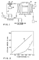
- Fig. 1 shows the outline of the manufacturing apparatus of the first embodiment whose function and use will be given hereinbelow.
- an object substrate (silicon wafer) 11 is inserted into a quartz tube 10 serving as a deposition chamber.
- the pressure within the quartz tube 10 is reduced with an exhaust pump 12, to introduce gaseous He and gaseous SiH4 from a He gas source 10A and SiH4 gas source 10B, respectively.
- the wafer 11 within the tube 10 is heated to around 600°C with an external heater 13.
- a polysilicon film is deposited on the wafer 11.
- the above-described reduced pressure CVD apparatus is coupled to a plasma discharge chamber in which gaseous CF4 and gaseous O2 from a CF4 gas source 14A and O2 gas source 14B, respectively, can be introduced via an introduction tube 17.
- gaseous CF4 and gaseous O2 from a CF4 gas source 14A and O2 gas source 14B, respectively can be introduced via an introduction tube 17.
- power is supplied from a microwave power source 15 to the discharge chamber 14 to generate a plasma 16 of the mixed gas.
- reference numeral 21 represents a flow regulator for regulating the flow ratio of O2 to CF4
- reference numeral 22 represents a temperature regulator for regulating the temperature of an intermediate semiconductor device within the tube 10 under control of the heater 13.
- a silicon wafer with a partially exposed polysilicon layer or a partially exposed diffused layer is subjected to cleaning, washing and drying processes using ordinary chemicals and thereafter, it is inserted into the quartz tube 10.
- the pressure within the tube 10 is reduced to about 10 ⁇ 2 Torr using the exhaust pump 12, with the temperature of the wafer being raised up to 600°C.
- air within the discharge chamber 14 is exhausted using the exhaust pump 12 to introduce therein a CF4 gas and an O2 gas to about 0.1 Torr under the condition of a flow ratio O2/(total gas flow) of about 50%.
- Microwave power is applied from the microwave power source 15 to the discharge chamber 14 to generate a plasma. Active species F* generated by the plasma are introduced into the deposition chamber 10.
- the etching speeds of Si and SiO2 under the active species F* relative to the temperature of the wafer are shown in Fig. 2. Particularly, at the low temperature range (room temperature to 150°C), a difference between the etching speeds of Si and SiO2 is large, whereas at the temperature range over 400°C, the difference becomes small. Therefore, by applying the active species F* to the silicon wafer heated to 600°C, polysilicon diffused layer and oxide film thereof are etched for a time sufficient for etching the very thin silicon oxide film (50 to 100 ⁇ ) formed on the exposed polysilicon or the exposed diffused layer. In this case, these are etched to the same degree. Thus, the difference between the etching speeds of the polysilicon and diffused layer, and oxide film thereof can be substantially neglected. After etching the oxide film, the reduced pressure CVD method is performed using He gas and SiH4 gas.
- polysilicon containing impurities can be deposited by using a gas containing impurities such as As, B, P and the like, or a silicon nitride film can be deposited by using ammonia.
- the apparatus of the second embodiment has a reduced pressure CVD apparatus for deposition of a polysilicon or silicon nitride film, the surface processing chamber and film deposition chamber thereof being separately mounted.
- An object wafer substrate similar to the first embodiment is transported into a load chamber 3-1 which is then subjected to vacuum exhaustion. Thereafter, a gate valve 3-2 is opened to move the wafer 3-3 to a cleaning chamber 3-4 as shown in Fig. 3.
- the cleaning chamber 3-4 is always maintained at reduced pressure by means of an air exhausting system 3-9.
- the temperature of the wafer 3-3 within the cleaning chamber 3-4 is rapidly raised to 600°C by means of an infrared heater 3-5 through a quartz glass window 3-17.
- a valve 3-7 between the cleaning chamber 3-4 and discharge chamber 3-6 is opened, and a mixed gas of CF4 and O2 is introduced into the discharge chamber 3-6.
- the wafer 3-14 with polysilicon deposited thereon as above is transported into an unload chamber 3-16 via a gate valve 3-20. Thereafter, a gas introduction system 3-15 is caused to operate so that active species are introduced from the discharge chamber 3-6 to the deposition chamber 3-10 to therefore effectively remove polysilicon attached on the inner wall of the deposition chamber 3-10.
- reference numeral 3-21 represents a flow regulator for regulating the flow ratio of O2 to CF4 (flow regulator in Fig. 8 is indicated at 8-21, and in Fig. 10 at 10-21), and reference numeral 3-22 represents a temperature regulator for regulating the temperature of an intermediate semiconductor device during etching (temperature regulator in Fig. 8 is indicated at 8-22, and in Fig. 10 at 10-22).
- the infrared heaters 3-5 and 3-12 have been used for heating the wafers 3-3 and 3-14, respectively.
- other heating means such as resistive wire heating means and induction heating means may also be used with the similar effects as above.
- etching in the cleaning chamber 3-4 is carried out at a high temperature but cleaning may be carried out at lower temperatures, e.g., near room temperature if the ratio of O2 to CF4 of the gases to be introduced into the discharge chamber 3-6 is changed.
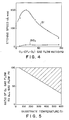
- Fig. 4 illustrates a change in the etching speeds of polysilicon and silicon oxide film relative to the ratio of O2 to (CF4 + O2) at the room temperature.
- the amount of O2 increases, the difference between the etching speeds of Si and SiO2 becomes correspondingly small.
- a relatively large amount of O2 allows an oxide film on the silicon surface to be properly removed even at room temperature.
- a significant point in the surface processing described in the second embodiment is that the difference between the etching speeds of silicon and silicon oxide is made as small as possible.
- the present inventors have thoroughly studied the etching of oxide films by using a mixed gas of a gaseous halogen compound and gaseous oxygen and have discovered that the gas flow ratio and temperature are important parameters. Taking into consideration the thickness of an oxide film and uniformity of etching, it can be judged that a practical value for the etching speed ratio of silicon to silicon oxide, is 5 or less. The region satisfying such a condition is indicated by oblique lines in Fig. 5.
- This region is given by the following formula: Y ⁇ -0.13 T + 106.3 where Y is a flow ratio in percent of the O2 gas to the total gas, and T (°C) is the temperature of a substrate.
- Y is a flow ratio in percent of the O2 gas to the total gas
- T (°C) is the temperature of a substrate.
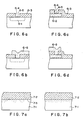
- Figs. 6a to 6d schematically show the processes of making polysilicon containing impurities come into contact with an underlying silicon diffused layer 6-1 (Figs. 6a and 6b) and with an underlying polysilicon layer containing impurities 6-2 (Figs. 6c and 6d).
- insulating layers 6-3 such as a silicon oxide film are deposited on the underlying diffused layer 6-1 or on the underlying polysilicon layer 6-2.
- contact holes 6-4 are formed above the insulating layers 6-3 for deposition of conductive polysilicon.
- thin natural oxide films 6-5 may grow on the surface of the polysilicon layer 6-2 or silicon diffused layer 6-1.
- the oxide film 6-5 is likely to grow much if impurities are contained in the underlying silicon or polysilicon layers. Electrical connection is not ensured even if polysilicon is deposited on the oxide film 6-5 but in this case, by using the embodiment apparatus, the oxide film 6-5 can be removed properly. Immediately after this removal, upper polysiliicon layers 6-6 can be deposited in the succeeding process to therefore allow satisfactory electrical connection (Figs. 6b and 6d).
- Figs. 7a and 7b Other applications of the above embodiments to a process of diffusing impurities into a silicon substrate are shown in Figs. 7a and 7b.
- a silicon oxide 7-2 containing impurities such as As, P and B is deposited on a silicon substrate 7-1. Thereafter, the impurities within the silicon oxide 7-2 are diffused into the silicon substrate 7-1 by means of heat treatment. If an oxide film 7-3 is present on the surface of the substrate 7-1 during the above processes, the diffusion at that portion is hindered (Fig. 7a).
- the above embodiments are applicable to a silicon nitride film forming process, although this is not shown.
- a silicon oxide film, polysilicon and silicon nitride film are deposited on a silicon substrate in this sequence.
- the silicon nitride film is patterned in a predetermined shape to use it as a selective oxidation mask for forming a field region (field oxide film).
- the oxide film inevitably formed on the polysilicon at the process of depositing the silicon nitride on the polysilicon can be removed so that abnormal oxidation during field oxidation can be avoided to therefore allow the formation of fine field regions.
- FIG. 8 A third embodiment is shown in Fig. 8 wherein the above-described cleaning means is mounted on a sputtering apparatus having a load lock mechanism.
- an object silicon wafer substrate 8-2 is transported from a load chamber 8-3 into an airtight cleaning chamber 8-1.
- the waer 8-2 is heated by an external infrared heater 8-4 through a quartz glass window 8-5.
- the cleaning chamber 8-1 is adapted to produce a vacuum by means of an air exhaust pump 8-6.
- the cleaning chamber 8-1 is coupled to a discharge chamber 8-7 which has a structure similar to the discharge chamber 3-6 shown in Fig. 3.
- a deposition chamber 8-8 for performing ordinary sputtering is mounted next the cleaning chamber 8-1.
- For the deposition chamber 8-8 there are provided a sputtering target 8-9, a silicon wafer 8-10 facing the target, a d.c.
- Reference numeral 8-11 represents a microwave power source
- 8-15, 8-18 and 8-19 represent a gate valve.
- an object wafer 8-2 is transported from the load chamber 8-3 into the cleaning chamber 8-1 as shown in Fig. 8.
- the inside of the load cleaning chamber 8-1 and discharge chamber 8-7 is made in a state of high vacuum state because of air exhaustion by means of an air exhaust system 8-6.
- a mixture gas of Cl2, NF3 and O2 is introduced into the discharge chamber 8-7 at about 0.1 Torr, and microwave power is supplied thereto from the microwave power source 8-13.
- discharge occurs within the discharge chamber 8-7 so that a number of active species are generated within the discharge chamber 8-7.
- the active species are introduced via an introduction system 8-14 into the cleaning chamber 8-1.
- the wafer 8-1 within the cleaning chamber 8-1 has been heated with the infrared heater 8-4 to have a temperature of about 450°C at the wafer surface.
- a silicon oxide film on the surface of the wafer 8-2 can be easily etched out with the active species containing the radical of Cl or F.
- the reaction speeds of silicon and silicon oxide with the active species are substantially equal to each other at such a high temperature. Therefore, the underlying silicon is scarcely damaged while removing the thin silicon oxide film formed thereon.
- the gate valve 8-15 is opened to transport the wafer 8-2 into the deposition chamber 8-8 to deposit an aluminum film for Al wiring on the silicon surface by means of sputtering. It was confirmed that the yield (provability) of electric connection between the underlying first layer and the Al wiring second layer improved remarkably.
- the cleaning chamber 8-1 and deposition chamber 8-8 have been provided separately in the apparatus shown in Fig. 8. However, they may be united into a single chamber to perform cleaning and deposition continuously and sequentially. Particularly in such a case, when a wafer is transported into a reaction chamber (single chamber), the reaction chamber is exhausted to have a vacuum and simultaneously therewith, the wafer is heated. Then, active species are introduced into the reaction chamber to remove an alumina layer 9-4 formed on an Al wiring first layer 9-1. Thereafter, the reaction chamber is again exhausted to create a high vacuum. Then, a gas such as Ar is introduced to deposit an Al wiring second layer through D.C. discharge sputtering.
- a fourth embodiment will be described with reference to Fig. 9, which uses a cold wall type, reduced pressure CVD apparatus with a load lock mechanism.
- a cleaning chamber 10-1 of the apparatus shown in Fig. 9 has the same structure as the cleaning chamber 8-1 shown in Fig. 8.
- a deposition chamber 10-2 for selective CVD of tungsten is mounted next the cleaning chamber 10-1.
- an air exhaust pump 10-3, infrared heater 10-4, and quartz glass window 105 adapted so as to introduce WF6 and H2.
- Reference numeral 10-6 represents an air exhaust pump, 10-8 a microwave power source, 10-9 an infrared heater, 10-10 a quartz glass window, 10-11 a load chamber, 10-12 and 10-13 a wafer, and 10-15 to 10-17 a gate valve.
- a silicon wafer with or without contact holes formed therein (refer to hole 6-4 in Fig. 6a) is subjected to cleaning, washing and drying processes using ordinary chemicals and thereafter, transported into the cleaning chamber 10-1 into which active species generated within the discharge chamber 10-7 are introduced.
- a thin natural oxide film (refer to film 6-5 in Fig. 6a) formed on the silicon surface exposed to atmosphere at the bottom of contact hole can be easily etched out with the active species. Therefore, the silicon surface (refer to surface 6-1 in Fig. 6a) becomes clean without an oxide film.
- the silicon surface is covered with a silicon oxide film which has been soiled considerably mainly due to organic substances, typically vacuum pump oil.
- the active species generated from the mixed gas of CF4 and O2 effectively etch out such organic substances.
- the active species slightly etch out the silicon oxide film so that the contaminated layer on the silicon surface can be completely removed and therefore expose an original, clean silicon oxide film.
- the inside of the cleaning chamber 10-1 is exhausted by means of the air exhaustion pump 10-6, and the wafer 10-12 is transported into the deposition chamber 10-2 which has been previously maintained vacuum by means of the air exhaust pump 10-3 so that the surface of the wafer 10-13 can be maintained clean.
- a mixture gas of WF6 and H2 is introduced into the deposition chamber 10-2 to selectively deposit W onto contact holes using the ordinary deposition conditions.
- the surfaces of the silicon and silicon oxide film are maintained sufficiently clean for presenting their intrinsic performance, so that selective deposition of W which is sensitive to the surface condition can be realized.
- the discharge chamber may be mounted on an epitaxial growing deposition apparatus wherein dry cleaning the deposition surface is performed, prior to the deposition, at relatively low temperature of 500 to 600°C using active species and thereafter, epitaxial growing is effected.
- the description has been directed to the case where an oxide film on the surface of silicon or aluminum is removed using CF4, NF3 or Cl2.
- the present invention is also applicable to other underlying materials such as high melting point metal, silicon compounds and the like, so long as the processes are performed for the purpose of improving contact between the underlying and overlaid layers by removing an oxide film or improving the overlaid film quality.
- other halogen compound gases such as CHF3, CFCl3 and the like may be used.
- the apparatus shown in Fig. 1 is used in this example.
- a substrate is inserted into the quartz tube 10 which is then subjected to pressure reduction. Thereafter, the silicon substrate is cleaned in the manner similar to the foregoing description. Then, an oxidizing gas such as O2 or H2O is introduced into the quartz tube 10 to oxidize the silicon and grow a silicon oxide film.
- the grown silicon oxide film can be used as a gate oxide film having a good breakdown voltage.
Landscapes
- Drying Of Semiconductors (AREA)
- Formation Of Insulating Films (AREA)
- Weting (AREA)
Applications Claiming Priority (2)
| Application Number | Priority Date | Filing Date | Title |
|---|---|---|---|
| JP73628/88 | 1988-03-28 | ||
| JP63073628A JP2768685B2 (ja) | 1988-03-28 | 1988-03-28 | 半導体装置の製造方法及びその装置 |
Publications (2)
| Publication Number | Publication Date |
|---|---|
| EP0335313A2 true EP0335313A2 (de) | 1989-10-04 |
| EP0335313A3 EP0335313A3 (de) | 1991-03-06 |
Family
ID=13523770
Family Applications (1)
| Application Number | Title | Priority Date | Filing Date |
|---|---|---|---|
| EP19890105425 Ceased EP0335313A3 (de) | 1988-03-28 | 1989-03-28 | Verfahren zur Herstellung eines Halbleiterbauelementes und hierzu verwendeter Apparat |
Country Status (4)
| Country | Link |
|---|---|
| US (1) | US5067437A (de) |
| EP (1) | EP0335313A3 (de) |
| JP (1) | JP2768685B2 (de) |
| KR (1) | KR920006261B1 (de) |
Cited By (2)
| Publication number | Priority date | Publication date | Assignee | Title |
|---|---|---|---|---|
| EP0413239A3 (en) * | 1989-08-14 | 1991-12-11 | Applied Materials Inc. | Gas distribution system |
| NL1009767C2 (nl) * | 1998-07-29 | 2000-02-04 | Asm Int | Werkwijze en inrichting voor het etsen van een substraat. |
Families Citing this family (298)
| Publication number | Priority date | Publication date | Assignee | Title |
|---|---|---|---|---|
| JPH01298181A (ja) * | 1988-05-25 | 1989-12-01 | Hitachi Ltd | ドライエッチング方法 |
| JP2744934B2 (ja) * | 1989-07-25 | 1998-04-28 | 東京エレクトロン株式会社 | 縦型処理装置 |
| US6047713A (en) * | 1994-02-03 | 2000-04-11 | Applied Materials, Inc. | Method for cleaning a throttle valve |
| US5425810A (en) * | 1994-05-11 | 1995-06-20 | Internation Business Machines Corporation | Removable gas injectors for use in chemical vapor deposition of aluminium oxide |
| KR100472175B1 (ko) * | 1997-08-25 | 2005-06-28 | 삼성전자주식회사 | 몰리브덴또는몰리브덴합금을이용한반도체장치의제조방법 |
| US5877064A (en) * | 1997-07-15 | 1999-03-02 | Taiwan Semiconductor Manufacturing Co.Ltd | Method for marking a wafer |
| US6352593B1 (en) * | 1997-08-11 | 2002-03-05 | Torrex Equipment Corp. | Mini-batch process chamber |
| US6352594B2 (en) * | 1997-08-11 | 2002-03-05 | Torrex | Method and apparatus for improved chemical vapor deposition processes using tunable temperature controlled gas injectors |
| US7393561B2 (en) * | 1997-08-11 | 2008-07-01 | Applied Materials, Inc. | Method and apparatus for layer by layer deposition of thin films |
| US20030049372A1 (en) * | 1997-08-11 | 2003-03-13 | Cook Robert C. | High rate deposition at low pressures in a small batch reactor |
| US6749687B1 (en) * | 1998-01-09 | 2004-06-15 | Asm America, Inc. | In situ growth of oxide and silicon layers |
| US6432830B1 (en) * | 1998-05-15 | 2002-08-13 | Applied Materials, Inc. | Semiconductor fabrication process |
| US6348420B1 (en) | 1999-12-23 | 2002-02-19 | Asm America, Inc. | Situ dielectric stacks |
| JP5089121B2 (ja) * | 2006-09-29 | 2012-12-05 | 東京エレクトロン株式会社 | シリコン酸化膜の形成方法およびプラズマ処理装置 |
| TWI421913B (zh) * | 2008-08-26 | 2014-01-01 | He Jian Technology Suzhou Co Ltd | 一種在爐管中沉積多晶矽的方法 |
| US20130023129A1 (en) | 2011-07-20 | 2013-01-24 | Asm America, Inc. | Pressure transmitter for a semiconductor processing environment |
| CN103545162B (zh) * | 2012-07-09 | 2016-06-08 | 北京北方微电子基地设备工艺研究中心有限责任公司 | 等离子体反应装置和石英窗加热方法 |
| US10714315B2 (en) | 2012-10-12 | 2020-07-14 | Asm Ip Holdings B.V. | Semiconductor reaction chamber showerhead |
| US20160376700A1 (en) | 2013-02-01 | 2016-12-29 | Asm Ip Holding B.V. | System for treatment of deposition reactor |
| US9099481B2 (en) | 2013-03-15 | 2015-08-04 | Semiconductor Components Industries, Llc | Methods of laser marking semiconductor substrates |
| US11015245B2 (en) | 2014-03-19 | 2021-05-25 | Asm Ip Holding B.V. | Gas-phase reactor and system having exhaust plenum and components thereof |
| US10858737B2 (en) | 2014-07-28 | 2020-12-08 | Asm Ip Holding B.V. | Showerhead assembly and components thereof |
| US10941490B2 (en) | 2014-10-07 | 2021-03-09 | Asm Ip Holding B.V. | Multiple temperature range susceptor, assembly, reactor and system including the susceptor, and methods of using the same |
| US10276355B2 (en) | 2015-03-12 | 2019-04-30 | Asm Ip Holding B.V. | Multi-zone reactor, system including the reactor, and method of using the same |
| US10458018B2 (en) | 2015-06-26 | 2019-10-29 | Asm Ip Holding B.V. | Structures including metal carbide material, devices including the structures, and methods of forming same |
| US10211308B2 (en) | 2015-10-21 | 2019-02-19 | Asm Ip Holding B.V. | NbMC layers |
| US11139308B2 (en) | 2015-12-29 | 2021-10-05 | Asm Ip Holding B.V. | Atomic layer deposition of III-V compounds to form V-NAND devices |
| US10529554B2 (en) | 2016-02-19 | 2020-01-07 | Asm Ip Holding B.V. | Method for forming silicon nitride film selectively on sidewalls or flat surfaces of trenches |
| US10343920B2 (en) | 2016-03-18 | 2019-07-09 | Asm Ip Holding B.V. | Aligned carbon nanotubes |
| US10367080B2 (en) | 2016-05-02 | 2019-07-30 | Asm Ip Holding B.V. | Method of forming a germanium oxynitride film |
| US11453943B2 (en) | 2016-05-25 | 2022-09-27 | Asm Ip Holding B.V. | Method for forming carbon-containing silicon/metal oxide or nitride film by ALD using silicon precursor and hydrocarbon precursor |
| US9859151B1 (en) | 2016-07-08 | 2018-01-02 | Asm Ip Holding B.V. | Selective film deposition method to form air gaps |
| US10612137B2 (en) | 2016-07-08 | 2020-04-07 | Asm Ip Holdings B.V. | Organic reactants for atomic layer deposition |
| US9812320B1 (en) | 2016-07-28 | 2017-11-07 | Asm Ip Holding B.V. | Method and apparatus for filling a gap |
| KR102532607B1 (ko) | 2016-07-28 | 2023-05-15 | 에이에스엠 아이피 홀딩 비.브이. | 기판 가공 장치 및 그 동작 방법 |
| US9887082B1 (en) | 2016-07-28 | 2018-02-06 | Asm Ip Holding B.V. | Method and apparatus for filling a gap |
| US11532757B2 (en) | 2016-10-27 | 2022-12-20 | Asm Ip Holding B.V. | Deposition of charge trapping layers |
| US10714350B2 (en) | 2016-11-01 | 2020-07-14 | ASM IP Holdings, B.V. | Methods for forming a transition metal niobium nitride film on a substrate by atomic layer deposition and related semiconductor device structures |
| KR102546317B1 (ko) | 2016-11-15 | 2023-06-21 | 에이에스엠 아이피 홀딩 비.브이. | 기체 공급 유닛 및 이를 포함하는 기판 처리 장치 |
| KR102762543B1 (ko) | 2016-12-14 | 2025-02-05 | 에이에스엠 아이피 홀딩 비.브이. | 기판 처리 장치 |
| US11447861B2 (en) | 2016-12-15 | 2022-09-20 | Asm Ip Holding B.V. | Sequential infiltration synthesis apparatus and a method of forming a patterned structure |
| US11581186B2 (en) | 2016-12-15 | 2023-02-14 | Asm Ip Holding B.V. | Sequential infiltration synthesis apparatus |
| KR102700194B1 (ko) | 2016-12-19 | 2024-08-28 | 에이에스엠 아이피 홀딩 비.브이. | 기판 처리 장치 |
| US10269558B2 (en) | 2016-12-22 | 2019-04-23 | Asm Ip Holding B.V. | Method of forming a structure on a substrate |
| US11390950B2 (en) | 2017-01-10 | 2022-07-19 | Asm Ip Holding B.V. | Reactor system and method to reduce residue buildup during a film deposition process |
| US10468261B2 (en) | 2017-02-15 | 2019-11-05 | Asm Ip Holding B.V. | Methods for forming a metallic film on a substrate by cyclical deposition and related semiconductor device structures |
| US10529563B2 (en) | 2017-03-29 | 2020-01-07 | Asm Ip Holdings B.V. | Method for forming doped metal oxide films on a substrate by cyclical deposition and related semiconductor device structures |
| US10770286B2 (en) | 2017-05-08 | 2020-09-08 | Asm Ip Holdings B.V. | Methods for selectively forming a silicon nitride film on a substrate and related semiconductor device structures |
| US12040200B2 (en) | 2017-06-20 | 2024-07-16 | Asm Ip Holding B.V. | Semiconductor processing apparatus and methods for calibrating a semiconductor processing apparatus |
| US11306395B2 (en) | 2017-06-28 | 2022-04-19 | Asm Ip Holding B.V. | Methods for depositing a transition metal nitride film on a substrate by atomic layer deposition and related deposition apparatus |
| KR20190009245A (ko) | 2017-07-18 | 2019-01-28 | 에이에스엠 아이피 홀딩 비.브이. | 반도체 소자 구조물 형성 방법 및 관련된 반도체 소자 구조물 |
| US11018002B2 (en) | 2017-07-19 | 2021-05-25 | Asm Ip Holding B.V. | Method for selectively depositing a Group IV semiconductor and related semiconductor device structures |
| US10541333B2 (en) | 2017-07-19 | 2020-01-21 | Asm Ip Holding B.V. | Method for depositing a group IV semiconductor and related semiconductor device structures |
| US11374112B2 (en) | 2017-07-19 | 2022-06-28 | Asm Ip Holding B.V. | Method for depositing a group IV semiconductor and related semiconductor device structures |
| US10590535B2 (en) | 2017-07-26 | 2020-03-17 | Asm Ip Holdings B.V. | Chemical treatment, deposition and/or infiltration apparatus and method for using the same |
| TWI815813B (zh) | 2017-08-04 | 2023-09-21 | 荷蘭商Asm智慧財產控股公司 | 用於分配反應腔內氣體的噴頭總成 |
| US10770336B2 (en) | 2017-08-08 | 2020-09-08 | Asm Ip Holding B.V. | Substrate lift mechanism and reactor including same |
| US10692741B2 (en) | 2017-08-08 | 2020-06-23 | Asm Ip Holdings B.V. | Radiation shield |
| US11139191B2 (en) | 2017-08-09 | 2021-10-05 | Asm Ip Holding B.V. | Storage apparatus for storing cassettes for substrates and processing apparatus equipped therewith |
| US11769682B2 (en) | 2017-08-09 | 2023-09-26 | Asm Ip Holding B.V. | Storage apparatus for storing cassettes for substrates and processing apparatus equipped therewith |
| US11830730B2 (en) | 2017-08-29 | 2023-11-28 | Asm Ip Holding B.V. | Layer forming method and apparatus |
| US11056344B2 (en) | 2017-08-30 | 2021-07-06 | Asm Ip Holding B.V. | Layer forming method |
| US11295980B2 (en) | 2017-08-30 | 2022-04-05 | Asm Ip Holding B.V. | Methods for depositing a molybdenum metal film over a dielectric surface of a substrate by a cyclical deposition process and related semiconductor device structures |
| KR102491945B1 (ko) | 2017-08-30 | 2023-01-26 | 에이에스엠 아이피 홀딩 비.브이. | 기판 처리 장치 |
| US10658205B2 (en) | 2017-09-28 | 2020-05-19 | Asm Ip Holdings B.V. | Chemical dispensing apparatus and methods for dispensing a chemical to a reaction chamber |
| US10403504B2 (en) | 2017-10-05 | 2019-09-03 | Asm Ip Holding B.V. | Method for selectively depositing a metallic film on a substrate |
| US10923344B2 (en) | 2017-10-30 | 2021-02-16 | Asm Ip Holding B.V. | Methods for forming a semiconductor structure and related semiconductor structures |
| US11022879B2 (en) | 2017-11-24 | 2021-06-01 | Asm Ip Holding B.V. | Method of forming an enhanced unexposed photoresist layer |
| TWI791689B (zh) | 2017-11-27 | 2023-02-11 | 荷蘭商Asm智慧財產控股私人有限公司 | 包括潔淨迷你環境之裝置 |
| JP7214724B2 (ja) | 2017-11-27 | 2023-01-30 | エーエスエム アイピー ホールディング ビー.ブイ. | バッチ炉で利用されるウェハカセットを収納するための収納装置 |
| US10872771B2 (en) | 2018-01-16 | 2020-12-22 | Asm Ip Holding B. V. | Method for depositing a material film on a substrate within a reaction chamber by a cyclical deposition process and related device structures |
| TWI799494B (zh) | 2018-01-19 | 2023-04-21 | 荷蘭商Asm 智慧財產控股公司 | 沈積方法 |
| KR102695659B1 (ko) | 2018-01-19 | 2024-08-14 | 에이에스엠 아이피 홀딩 비.브이. | 플라즈마 보조 증착에 의해 갭 충진 층을 증착하는 방법 |
| US11081345B2 (en) | 2018-02-06 | 2021-08-03 | Asm Ip Holding B.V. | Method of post-deposition treatment for silicon oxide film |
| US10896820B2 (en) | 2018-02-14 | 2021-01-19 | Asm Ip Holding B.V. | Method for depositing a ruthenium-containing film on a substrate by a cyclical deposition process |
| US11685991B2 (en) | 2018-02-14 | 2023-06-27 | Asm Ip Holding B.V. | Method for depositing a ruthenium-containing film on a substrate by a cyclical deposition process |
| US10731249B2 (en) | 2018-02-15 | 2020-08-04 | Asm Ip Holding B.V. | Method of forming a transition metal containing film on a substrate by a cyclical deposition process, a method for supplying a transition metal halide compound to a reaction chamber, and related vapor deposition apparatus |
| KR102636427B1 (ko) | 2018-02-20 | 2024-02-13 | 에이에스엠 아이피 홀딩 비.브이. | 기판 처리 방법 및 장치 |
| US10975470B2 (en) | 2018-02-23 | 2021-04-13 | Asm Ip Holding B.V. | Apparatus for detecting or monitoring for a chemical precursor in a high temperature environment |
| US11473195B2 (en) | 2018-03-01 | 2022-10-18 | Asm Ip Holding B.V. | Semiconductor processing apparatus and a method for processing a substrate |
| US11629406B2 (en) | 2018-03-09 | 2023-04-18 | Asm Ip Holding B.V. | Semiconductor processing apparatus comprising one or more pyrometers for measuring a temperature of a substrate during transfer of the substrate |
| US11114283B2 (en) | 2018-03-16 | 2021-09-07 | Asm Ip Holding B.V. | Reactor, system including the reactor, and methods of manufacturing and using same |
| KR102646467B1 (ko) | 2018-03-27 | 2024-03-11 | 에이에스엠 아이피 홀딩 비.브이. | 기판 상에 전극을 형성하는 방법 및 전극을 포함하는 반도체 소자 구조 |
| US11088002B2 (en) | 2018-03-29 | 2021-08-10 | Asm Ip Holding B.V. | Substrate rack and a substrate processing system and method |
| US11230766B2 (en) | 2018-03-29 | 2022-01-25 | Asm Ip Holding B.V. | Substrate processing apparatus and method |
| KR102600229B1 (ko) | 2018-04-09 | 2023-11-10 | 에이에스엠 아이피 홀딩 비.브이. | 기판 지지 장치, 이를 포함하는 기판 처리 장치 및 기판 처리 방법 |
| US12025484B2 (en) | 2018-05-08 | 2024-07-02 | Asm Ip Holding B.V. | Thin film forming method |
| TWI843623B (zh) | 2018-05-08 | 2024-05-21 | 荷蘭商Asm Ip私人控股有限公司 | 藉由循環沉積製程於基板上沉積氧化物膜之方法及相關裝置結構 |
| US12272527B2 (en) | 2018-05-09 | 2025-04-08 | Asm Ip Holding B.V. | Apparatus for use with hydrogen radicals and method of using same |
| KR102596988B1 (ko) | 2018-05-28 | 2023-10-31 | 에이에스엠 아이피 홀딩 비.브이. | 기판 처리 방법 및 그에 의해 제조된 장치 |
| TWI840362B (zh) | 2018-06-04 | 2024-05-01 | 荷蘭商Asm Ip私人控股有限公司 | 水氣降低的晶圓處置腔室 |
| US11718913B2 (en) | 2018-06-04 | 2023-08-08 | Asm Ip Holding B.V. | Gas distribution system and reactor system including same |
| US11286562B2 (en) | 2018-06-08 | 2022-03-29 | Asm Ip Holding B.V. | Gas-phase chemical reactor and method of using same |
| US10797133B2 (en) | 2018-06-21 | 2020-10-06 | Asm Ip Holding B.V. | Method for depositing a phosphorus doped silicon arsenide film and related semiconductor device structures |
| KR102568797B1 (ko) | 2018-06-21 | 2023-08-21 | 에이에스엠 아이피 홀딩 비.브이. | 기판 처리 시스템 |
| US11499222B2 (en) | 2018-06-27 | 2022-11-15 | Asm Ip Holding B.V. | Cyclic deposition methods for forming metal-containing material and films and structures including the metal-containing material |
| TWI871083B (zh) | 2018-06-27 | 2025-01-21 | 荷蘭商Asm Ip私人控股有限公司 | 用於形成含金屬材料之循環沉積製程 |
| US10612136B2 (en) | 2018-06-29 | 2020-04-07 | ASM IP Holding, B.V. | Temperature-controlled flange and reactor system including same |
| US10388513B1 (en) | 2018-07-03 | 2019-08-20 | Asm Ip Holding B.V. | Method for depositing silicon-free carbon-containing film as gap-fill layer by pulse plasma-assisted deposition |
| US10755922B2 (en) | 2018-07-03 | 2020-08-25 | Asm Ip Holding B.V. | Method for depositing silicon-free carbon-containing film as gap-fill layer by pulse plasma-assisted deposition |
| US11053591B2 (en) | 2018-08-06 | 2021-07-06 | Asm Ip Holding B.V. | Multi-port gas injection system and reactor system including same |
| US11430674B2 (en) | 2018-08-22 | 2022-08-30 | Asm Ip Holding B.V. | Sensor array, apparatus for dispensing a vapor phase reactant to a reaction chamber and related methods |
| US11024523B2 (en) | 2018-09-11 | 2021-06-01 | Asm Ip Holding B.V. | Substrate processing apparatus and method |
| KR102707956B1 (ko) | 2018-09-11 | 2024-09-19 | 에이에스엠 아이피 홀딩 비.브이. | 박막 증착 방법 |
| US11049751B2 (en) | 2018-09-14 | 2021-06-29 | Asm Ip Holding B.V. | Cassette supply system to store and handle cassettes and processing apparatus equipped therewith |
| CN110970344B (zh) | 2018-10-01 | 2024-10-25 | Asmip控股有限公司 | 衬底保持设备、包含所述设备的系统及其使用方法 |
| US11232963B2 (en) | 2018-10-03 | 2022-01-25 | Asm Ip Holding B.V. | Substrate processing apparatus and method |
| KR102592699B1 (ko) | 2018-10-08 | 2023-10-23 | 에이에스엠 아이피 홀딩 비.브이. | 기판 지지 유닛 및 이를 포함하는 박막 증착 장치와 기판 처리 장치 |
| KR102546322B1 (ko) | 2018-10-19 | 2023-06-21 | 에이에스엠 아이피 홀딩 비.브이. | 기판 처리 장치 및 기판 처리 방법 |
| KR102605121B1 (ko) | 2018-10-19 | 2023-11-23 | 에이에스엠 아이피 홀딩 비.브이. | 기판 처리 장치 및 기판 처리 방법 |
| USD948463S1 (en) | 2018-10-24 | 2022-04-12 | Asm Ip Holding B.V. | Susceptor for semiconductor substrate supporting apparatus |
| US12378665B2 (en) | 2018-10-26 | 2025-08-05 | Asm Ip Holding B.V. | High temperature coatings for a preclean and etch apparatus and related methods |
| US11087997B2 (en) | 2018-10-31 | 2021-08-10 | Asm Ip Holding B.V. | Substrate processing apparatus for processing substrates |
| KR102748291B1 (ko) | 2018-11-02 | 2024-12-31 | 에이에스엠 아이피 홀딩 비.브이. | 기판 지지 유닛 및 이를 포함하는 기판 처리 장치 |
| US11572620B2 (en) | 2018-11-06 | 2023-02-07 | Asm Ip Holding B.V. | Methods for selectively depositing an amorphous silicon film on a substrate |
| US11031242B2 (en) | 2018-11-07 | 2021-06-08 | Asm Ip Holding B.V. | Methods for depositing a boron doped silicon germanium film |
| US10818758B2 (en) | 2018-11-16 | 2020-10-27 | Asm Ip Holding B.V. | Methods for forming a metal silicate film on a substrate in a reaction chamber and related semiconductor device structures |
| US10847366B2 (en) | 2018-11-16 | 2020-11-24 | Asm Ip Holding B.V. | Methods for depositing a transition metal chalcogenide film on a substrate by a cyclical deposition process |
| US12040199B2 (en) | 2018-11-28 | 2024-07-16 | Asm Ip Holding B.V. | Substrate processing apparatus for processing substrates |
| US11217444B2 (en) | 2018-11-30 | 2022-01-04 | Asm Ip Holding B.V. | Method for forming an ultraviolet radiation responsive metal oxide-containing film |
| KR102636428B1 (ko) | 2018-12-04 | 2024-02-13 | 에이에스엠 아이피 홀딩 비.브이. | 기판 처리 장치를 세정하는 방법 |
| US11158513B2 (en) | 2018-12-13 | 2021-10-26 | Asm Ip Holding B.V. | Methods for forming a rhenium-containing film on a substrate by a cyclical deposition process and related semiconductor device structures |
| JP7504584B2 (ja) | 2018-12-14 | 2024-06-24 | エーエスエム・アイピー・ホールディング・ベー・フェー | 窒化ガリウムの選択的堆積を用いてデバイス構造体を形成する方法及びそのためのシステム |
| TWI866480B (zh) | 2019-01-17 | 2024-12-11 | 荷蘭商Asm Ip 私人控股有限公司 | 藉由循環沈積製程於基板上形成含過渡金屬膜之方法 |
| KR102727227B1 (ko) | 2019-01-22 | 2024-11-07 | 에이에스엠 아이피 홀딩 비.브이. | 기판 처리 장치 |
| CN111524788B (zh) | 2019-02-01 | 2023-11-24 | Asm Ip私人控股有限公司 | 氧化硅的拓扑选择性膜形成的方法 |
| TWI873122B (zh) | 2019-02-20 | 2025-02-21 | 荷蘭商Asm Ip私人控股有限公司 | 填充一基板之一表面內所形成的一凹槽的方法、根據其所形成之半導體結構、及半導體處理設備 |
| KR20200102357A (ko) | 2019-02-20 | 2020-08-31 | 에이에스엠 아이피 홀딩 비.브이. | 3-d nand 응용의 플러그 충진체 증착용 장치 및 방법 |
| KR102626263B1 (ko) | 2019-02-20 | 2024-01-16 | 에이에스엠 아이피 홀딩 비.브이. | 처리 단계를 포함하는 주기적 증착 방법 및 이를 위한 장치 |
| TWI845607B (zh) | 2019-02-20 | 2024-06-21 | 荷蘭商Asm Ip私人控股有限公司 | 用來填充形成於基材表面內之凹部的循環沉積方法及設備 |
| TWI842826B (zh) | 2019-02-22 | 2024-05-21 | 荷蘭商Asm Ip私人控股有限公司 | 基材處理設備及處理基材之方法 |
| KR102782593B1 (ko) | 2019-03-08 | 2025-03-14 | 에이에스엠 아이피 홀딩 비.브이. | SiOC 층을 포함한 구조체 및 이의 형성 방법 |
| KR102858005B1 (ko) | 2019-03-08 | 2025-09-09 | 에이에스엠 아이피 홀딩 비.브이. | 실리콘 질화물 층을 선택적으로 증착하는 방법, 및 선택적으로 증착된 실리콘 질화물 층을 포함하는 구조체 |
| KR102762833B1 (ko) | 2019-03-08 | 2025-02-04 | 에이에스엠 아이피 홀딩 비.브이. | SiOCN 층을 포함한 구조체 및 이의 형성 방법 |
| JP2020167398A (ja) | 2019-03-28 | 2020-10-08 | エーエスエム・アイピー・ホールディング・ベー・フェー | ドアオープナーおよびドアオープナーが提供される基材処理装置 |
| KR102809999B1 (ko) | 2019-04-01 | 2025-05-19 | 에이에스엠 아이피 홀딩 비.브이. | 반도체 소자를 제조하는 방법 |
| KR102897355B1 (ko) | 2019-04-19 | 2025-12-08 | 에이에스엠 아이피 홀딩 비.브이. | 층 형성 방법 및 장치 |
| KR20200125453A (ko) | 2019-04-24 | 2020-11-04 | 에이에스엠 아이피 홀딩 비.브이. | 기상 반응기 시스템 및 이를 사용하는 방법 |
| KR102869364B1 (ko) | 2019-05-07 | 2025-10-10 | 에이에스엠 아이피 홀딩 비.브이. | 비정질 탄소 중합체 막을 개질하는 방법 |
| KR102929471B1 (ko) | 2019-05-07 | 2026-02-20 | 에이에스엠 아이피 홀딩 비.브이. | 딥 튜브가 있는 화학물질 공급원 용기 |
| KR102929472B1 (ko) | 2019-05-10 | 2026-02-20 | 에이에스엠 아이피 홀딩 비.브이. | 표면 상에 재료를 증착하는 방법 및 본 방법에 따라 형성된 구조 |
| JP7612342B2 (ja) | 2019-05-16 | 2025-01-14 | エーエスエム・アイピー・ホールディング・ベー・フェー | ウェハボートハンドリング装置、縦型バッチ炉および方法 |
| JP7598201B2 (ja) | 2019-05-16 | 2024-12-11 | エーエスエム・アイピー・ホールディング・ベー・フェー | ウェハボートハンドリング装置、縦型バッチ炉および方法 |
| USD975665S1 (en) | 2019-05-17 | 2023-01-17 | Asm Ip Holding B.V. | Susceptor shaft |
| USD947913S1 (en) | 2019-05-17 | 2022-04-05 | Asm Ip Holding B.V. | Susceptor shaft |
| USD935572S1 (en) | 2019-05-24 | 2021-11-09 | Asm Ip Holding B.V. | Gas channel plate |
| USD922229S1 (en) | 2019-06-05 | 2021-06-15 | Asm Ip Holding B.V. | Device for controlling a temperature of a gas supply unit |
| KR20200141002A (ko) | 2019-06-06 | 2020-12-17 | 에이에스엠 아이피 홀딩 비.브이. | 배기 가스 분석을 포함한 기상 반응기 시스템을 사용하는 방법 |
| KR102918757B1 (ko) | 2019-06-10 | 2026-01-28 | 에이에스엠 아이피 홀딩 비.브이. | 석영 에피택셜 챔버를 세정하는 방법 |
| KR20200143254A (ko) | 2019-06-11 | 2020-12-23 | 에이에스엠 아이피 홀딩 비.브이. | 개질 가스를 사용하여 전자 구조를 형성하는 방법, 상기 방법을 수행하기 위한 시스템, 및 상기 방법을 사용하여 형성되는 구조 |
| USD944946S1 (en) | 2019-06-14 | 2022-03-01 | Asm Ip Holding B.V. | Shower plate |
| USD931978S1 (en) | 2019-06-27 | 2021-09-28 | Asm Ip Holding B.V. | Showerhead vacuum transport |
| KR102911421B1 (ko) | 2019-07-03 | 2026-01-12 | 에이에스엠 아이피 홀딩 비.브이. | 기판 처리 장치용 온도 제어 조립체 및 이를 사용하는 방법 |
| JP7499079B2 (ja) | 2019-07-09 | 2024-06-13 | エーエスエム・アイピー・ホールディング・ベー・フェー | 同軸導波管を用いたプラズマ装置、基板処理方法 |
| CN112216646B (zh) | 2019-07-10 | 2026-02-10 | Asmip私人控股有限公司 | 基板支撑组件及包括其的基板处理装置 |
| KR102895115B1 (ko) | 2019-07-16 | 2025-12-03 | 에이에스엠 아이피 홀딩 비.브이. | 기판 처리 장치 |
| KR102860110B1 (ko) | 2019-07-17 | 2025-09-16 | 에이에스엠 아이피 홀딩 비.브이. | 실리콘 게르마늄 구조를 형성하는 방법 |
| TWI826704B (zh) | 2019-07-17 | 2023-12-21 | 荷蘭商Asm Ip私人控股有限公司 | 自由基輔助引燃電漿系統和方法 |
| US11643724B2 (en) | 2019-07-18 | 2023-05-09 | Asm Ip Holding B.V. | Method of forming structures using a neutral beam |
| KR102903090B1 (ko) | 2019-07-19 | 2025-12-19 | 에이에스엠 아이피 홀딩 비.브이. | 토폴로지-제어된 비정질 탄소 중합체 막을 형성하는 방법 |
| TWI839544B (zh) | 2019-07-19 | 2024-04-21 | 荷蘭商Asm Ip私人控股有限公司 | 形成形貌受控的非晶碳聚合物膜之方法 |
| CN112309843B (zh) | 2019-07-29 | 2026-01-23 | Asmip私人控股有限公司 | 实现高掺杂剂掺入的选择性沉积方法 |
| CN112309899B (zh) | 2019-07-30 | 2025-11-14 | Asmip私人控股有限公司 | 基板处理设备 |
| KR20210015655A (ko) | 2019-07-30 | 2021-02-10 | 에이에스엠 아이피 홀딩 비.브이. | 기판 처리 장치 및 방법 |
| CN112309900B (zh) | 2019-07-30 | 2025-11-04 | Asmip私人控股有限公司 | 基板处理设备 |
| US11227782B2 (en) | 2019-07-31 | 2022-01-18 | Asm Ip Holding B.V. | Vertical batch furnace assembly |
| US11587814B2 (en) | 2019-07-31 | 2023-02-21 | Asm Ip Holding B.V. | Vertical batch furnace assembly |
| US11587815B2 (en) | 2019-07-31 | 2023-02-21 | Asm Ip Holding B.V. | Vertical batch furnace assembly |
| KR20210018759A (ko) | 2019-08-05 | 2021-02-18 | 에이에스엠 아이피 홀딩 비.브이. | 화학물질 공급원 용기를 위한 액체 레벨 센서 |
| KR20210018761A (ko) | 2019-08-09 | 2021-02-18 | 에이에스엠 아이피 홀딩 비.브이. | 냉각 장치를 포함한 히터 어셈블리 및 이를 사용하는 방법 |
| USD965044S1 (en) | 2019-08-19 | 2022-09-27 | Asm Ip Holding B.V. | Susceptor shaft |
| USD965524S1 (en) | 2019-08-19 | 2022-10-04 | Asm Ip Holding B.V. | Susceptor support |
| JP7810514B2 (ja) | 2019-08-21 | 2026-02-03 | エーエスエム・アイピー・ホールディング・ベー・フェー | 成膜原料混合ガス生成装置及び成膜装置 |
| USD930782S1 (en) | 2019-08-22 | 2021-09-14 | Asm Ip Holding B.V. | Gas distributor |
| USD949319S1 (en) | 2019-08-22 | 2022-04-19 | Asm Ip Holding B.V. | Exhaust duct |
| USD979506S1 (en) | 2019-08-22 | 2023-02-28 | Asm Ip Holding B.V. | Insulator |
| USD940837S1 (en) | 2019-08-22 | 2022-01-11 | Asm Ip Holding B.V. | Electrode |
| KR20210024423A (ko) | 2019-08-22 | 2021-03-05 | 에이에스엠 아이피 홀딩 비.브이. | 홀을 구비한 구조체를 형성하기 위한 방법 |
| KR102928101B1 (ko) | 2019-08-23 | 2026-02-13 | 에이에스엠 아이피 홀딩 비.브이. | 비스(디에틸아미노)실란을 사용하여 peald에 의해 개선된 품질을 갖는 실리콘 산화물 막을 증착하기 위한 방법 |
| US11286558B2 (en) | 2019-08-23 | 2022-03-29 | Asm Ip Holding B.V. | Methods for depositing a molybdenum nitride film on a surface of a substrate by a cyclical deposition process and related semiconductor device structures including a molybdenum nitride film |
| KR102868968B1 (ko) | 2019-09-03 | 2025-10-10 | 에이에스엠 아이피 홀딩 비.브이. | 칼코지나이드 막 및 상기 막을 포함한 구조체를 증착하기 위한 방법 및 장치 |
| KR102806450B1 (ko) | 2019-09-04 | 2025-05-12 | 에이에스엠 아이피 홀딩 비.브이. | 희생 캡핑 층을 이용한 선택적 증착 방법 |
| KR102733104B1 (ko) | 2019-09-05 | 2024-11-22 | 에이에스엠 아이피 홀딩 비.브이. | 기판 처리 장치 |
| US12469693B2 (en) | 2019-09-17 | 2025-11-11 | Asm Ip Holding B.V. | Method of forming a carbon-containing layer and structure including the layer |
| US11562901B2 (en) | 2019-09-25 | 2023-01-24 | Asm Ip Holding B.V. | Substrate processing method |
| CN112593212B (zh) | 2019-10-02 | 2023-12-22 | Asm Ip私人控股有限公司 | 通过循环等离子体增强沉积工艺形成拓扑选择性氧化硅膜的方法 |
| KR102948143B1 (ko) | 2019-10-08 | 2026-04-07 | 에이에스엠 아이피 홀딩 비.브이. | 활성 종을 이용하기 위한 가스 분배 어셈블리를 포함한 반응기 시스템 및 이를 사용하는 방법 |
| TW202128273A (zh) | 2019-10-08 | 2021-08-01 | 荷蘭商Asm Ip私人控股有限公司 | 氣體注入系統、及將材料沉積於反應室內之基板表面上的方法 |
| TWI846953B (zh) | 2019-10-08 | 2024-07-01 | 荷蘭商Asm Ip私人控股有限公司 | 基板處理裝置 |
| TWI846966B (zh) | 2019-10-10 | 2024-07-01 | 荷蘭商Asm Ip私人控股有限公司 | 形成光阻底層之方法及包括光阻底層之結構 |
| US12009241B2 (en) | 2019-10-14 | 2024-06-11 | Asm Ip Holding B.V. | Vertical batch furnace assembly with detector to detect cassette |
| TWI834919B (zh) | 2019-10-16 | 2024-03-11 | 荷蘭商Asm Ip私人控股有限公司 | 氧化矽之拓撲選擇性膜形成之方法 |
| US11637014B2 (en) | 2019-10-17 | 2023-04-25 | Asm Ip Holding B.V. | Methods for selective deposition of doped semiconductor material |
| KR102845724B1 (ko) | 2019-10-21 | 2025-08-13 | 에이에스엠 아이피 홀딩 비.브이. | 막을 선택적으로 에칭하기 위한 장치 및 방법 |
| US11996292B2 (en) | 2019-10-25 | 2024-05-28 | Asm Ip Holding B.V. | Methods for filling a gap feature on a substrate surface and related semiconductor structures |
| US11646205B2 (en) | 2019-10-29 | 2023-05-09 | Asm Ip Holding B.V. | Methods of selectively forming n-type doped material on a surface, systems for selectively forming n-type doped material, and structures formed using same |
| KR102890638B1 (ko) | 2019-11-05 | 2025-11-25 | 에이에스엠 아이피 홀딩 비.브이. | 도핑된 반도체 층을 갖는 구조체 및 이를 형성하기 위한 방법 및 시스템 |
| US11501968B2 (en) | 2019-11-15 | 2022-11-15 | Asm Ip Holding B.V. | Method for providing a semiconductor device with silicon filled gaps |
| KR102861314B1 (ko) | 2019-11-20 | 2025-09-17 | 에이에스엠 아이피 홀딩 비.브이. | 기판의 표면 상에 탄소 함유 물질을 증착하는 방법, 상기 방법을 사용하여 형성된 구조물, 및 상기 구조물을 형성하기 위한 시스템 |
| KR20210065848A (ko) | 2019-11-26 | 2021-06-04 | 에이에스엠 아이피 홀딩 비.브이. | 제1 유전체 표면과 제2 금속성 표면을 포함한 기판 상에 타겟 막을 선택적으로 형성하기 위한 방법 |
| CN112951697B (zh) | 2019-11-26 | 2025-07-29 | Asmip私人控股有限公司 | 基板处理设备 |
| CN112885692B (zh) | 2019-11-29 | 2025-08-15 | Asmip私人控股有限公司 | 基板处理设备 |
| CN120432376A (zh) | 2019-11-29 | 2025-08-05 | Asm Ip私人控股有限公司 | 基板处理设备 |
| JP7527928B2 (ja) | 2019-12-02 | 2024-08-05 | エーエスエム・アイピー・ホールディング・ベー・フェー | 基板処理装置、基板処理方法 |
| KR20210070898A (ko) | 2019-12-04 | 2021-06-15 | 에이에스엠 아이피 홀딩 비.브이. | 기판 처리 장치 |
| US11885013B2 (en) | 2019-12-17 | 2024-01-30 | Asm Ip Holding B.V. | Method of forming vanadium nitride layer and structure including the vanadium nitride layer |
| KR102943768B1 (ko) | 2019-12-19 | 2026-03-26 | 에이에스엠 아이피 홀딩 비.브이. | 기판 상의 갭 피처를 충진하는 방법 및 이와 관련된 반도체 소자 구조 |
| JP7730637B2 (ja) | 2020-01-06 | 2025-08-28 | エーエスエム・アイピー・ホールディング・ベー・フェー | ガス供給アセンブリ、その構成要素、およびこれを含む反応器システム |
| TWI887322B (zh) | 2020-01-06 | 2025-06-21 | 荷蘭商Asm Ip私人控股有限公司 | 反應器系統、抬升銷、及處理方法 |
| US11993847B2 (en) | 2020-01-08 | 2024-05-28 | Asm Ip Holding B.V. | Injector |
| KR102882467B1 (ko) | 2020-01-16 | 2025-11-05 | 에이에스엠 아이피 홀딩 비.브이. | 고 종횡비 피처를 형성하는 방법 |
| KR102675856B1 (ko) | 2020-01-20 | 2024-06-17 | 에이에스엠 아이피 홀딩 비.브이. | 박막 형성 방법 및 박막 표면 개질 방법 |
| TWI889744B (zh) | 2020-01-29 | 2025-07-11 | 荷蘭商Asm Ip私人控股有限公司 | 污染物捕集系統、及擋板堆疊 |
| TW202513845A (zh) | 2020-02-03 | 2025-04-01 | 荷蘭商Asm Ip私人控股有限公司 | 半導體裝置結構及其形成方法 |
| KR20210100010A (ko) | 2020-02-04 | 2021-08-13 | 에이에스엠 아이피 홀딩 비.브이. | 대형 물품의 투과율 측정을 위한 방법 및 장치 |
| US11776846B2 (en) | 2020-02-07 | 2023-10-03 | Asm Ip Holding B.V. | Methods for depositing gap filling fluids and related systems and devices |
| KR20210103953A (ko) | 2020-02-13 | 2021-08-24 | 에이에스엠 아이피 홀딩 비.브이. | 가스 분배 어셈블리 및 이를 사용하는 방법 |
| KR102916725B1 (ko) | 2020-02-13 | 2026-01-23 | 에이에스엠 아이피 홀딩 비.브이. | 수광 장치를 포함하는 기판 처리 장치 및 수광 장치의 교정 방법 |
| US11781243B2 (en) | 2020-02-17 | 2023-10-10 | Asm Ip Holding B.V. | Method for depositing low temperature phosphorous-doped silicon |
| TWI895326B (zh) | 2020-02-28 | 2025-09-01 | 荷蘭商Asm Ip私人控股有限公司 | 專用於零件清潔的系統 |
| KR102943116B1 (ko) | 2020-03-04 | 2026-03-23 | 에이에스엠 아이피 홀딩 비.브이. | 반응기 시스템용 정렬 고정구 |
| US11876356B2 (en) | 2020-03-11 | 2024-01-16 | Asm Ip Holding B.V. | Lockout tagout assembly and system and method of using same |
| KR20210116240A (ko) | 2020-03-11 | 2021-09-27 | 에이에스엠 아이피 홀딩 비.브이. | 조절성 접합부를 갖는 기판 핸들링 장치 |
| KR102775390B1 (ko) | 2020-03-12 | 2025-02-28 | 에이에스엠 아이피 홀딩 비.브이. | 타겟 토폴로지 프로파일을 갖는 층 구조를 제조하기 위한 방법 |
| US12173404B2 (en) | 2020-03-17 | 2024-12-24 | Asm Ip Holding B.V. | Method of depositing epitaxial material, structure formed using the method, and system for performing the method |
| KR102755229B1 (ko) | 2020-04-02 | 2025-01-14 | 에이에스엠 아이피 홀딩 비.브이. | 박막 형성 방법 |
| TWI887376B (zh) | 2020-04-03 | 2025-06-21 | 荷蘭商Asm Ip私人控股有限公司 | 半導體裝置的製造方法 |
| TWI888525B (zh) | 2020-04-08 | 2025-07-01 | 荷蘭商Asm Ip私人控股有限公司 | 用於選擇性蝕刻氧化矽膜之設備及方法 |
| US11821078B2 (en) | 2020-04-15 | 2023-11-21 | Asm Ip Holding B.V. | Method for forming precoat film and method for forming silicon-containing film |
| KR20210128343A (ko) | 2020-04-15 | 2021-10-26 | 에이에스엠 아이피 홀딩 비.브이. | 크롬 나이트라이드 층을 형성하는 방법 및 크롬 나이트라이드 층을 포함하는 구조 |
| US11996289B2 (en) | 2020-04-16 | 2024-05-28 | Asm Ip Holding B.V. | Methods of forming structures including silicon germanium and silicon layers, devices formed using the methods, and systems for performing the methods |
| KR102901748B1 (ko) | 2020-04-21 | 2025-12-17 | 에이에스엠 아이피 홀딩 비.브이. | 기판을 처리하기 위한 방법 |
| CN113555279A (zh) | 2020-04-24 | 2021-10-26 | Asm Ip私人控股有限公司 | 形成含氮化钒的层的方法及包含其的结构 |
| KR102934380B1 (ko) | 2020-04-24 | 2026-03-05 | 에이에스엠 아이피 홀딩 비.브이. | 바나듐 보라이드 및 바나듐 포스파이드 층을 포함한 구조체를 형성하는 방법 |
| KR20210132600A (ko) | 2020-04-24 | 2021-11-04 | 에이에스엠 아이피 홀딩 비.브이. | 바나듐, 질소 및 추가 원소를 포함한 층을 증착하기 위한 방법 및 시스템 |
| KR102866804B1 (ko) | 2020-04-24 | 2025-09-30 | 에이에스엠 아이피 홀딩 비.브이. | 냉각 가스 공급부를 포함한 수직형 배치 퍼니스 어셈블리 |
| TW202539998A (zh) | 2020-04-24 | 2025-10-16 | 荷蘭商Asm Ip私人控股有限公司 | 包含釩化合物之組成物與容器及用於穩定釩化合物之方法及系統 |
| KR102783898B1 (ko) | 2020-04-29 | 2025-03-18 | 에이에스엠 아이피 홀딩 비.브이. | 고체 소스 전구체 용기 |
| KR20210134869A (ko) | 2020-05-01 | 2021-11-11 | 에이에스엠 아이피 홀딩 비.브이. | Foup 핸들러를 이용한 foup의 빠른 교환 |
| JP7726664B2 (ja) | 2020-05-04 | 2025-08-20 | エーエスエム・アイピー・ホールディング・ベー・フェー | 基板を処理するための基板処理システム |
| JP7736446B2 (ja) | 2020-05-07 | 2025-09-09 | エーエスエム・アイピー・ホールディング・ベー・フェー | 同調回路を備える反応器システム |
| KR20210137395A (ko) | 2020-05-07 | 2021-11-17 | 에이에스엠 아이피 홀딩 비.브이. | 불소계 라디칼을 이용하여 반응 챔버의 인시츄 식각을 수행하기 위한 장치 및 방법 |
| KR102788543B1 (ko) | 2020-05-13 | 2025-03-27 | 에이에스엠 아이피 홀딩 비.브이. | 반응기 시스템용 레이저 정렬 고정구 |
| KR102936676B1 (ko) | 2020-05-15 | 2026-03-10 | 에이에스엠 아이피 홀딩 비.브이. | 다중 전구체를 사용하여 실리콘 게르마늄 균일도를 제어하기 위한 방법 |
| KR102905441B1 (ko) | 2020-05-19 | 2025-12-30 | 에이에스엠 아이피 홀딩 비.브이. | 기판 처리 장치 |
| KR102795476B1 (ko) | 2020-05-21 | 2025-04-11 | 에이에스엠 아이피 홀딩 비.브이. | 다수의 탄소 층을 포함한 구조체 및 이를 형성하고 사용하는 방법 |
| KR20210145079A (ko) | 2020-05-21 | 2021-12-01 | 에이에스엠 아이피 홀딩 비.브이. | 기판을 처리하기 위한 플랜지 및 장치 |
| TWI873343B (zh) | 2020-05-22 | 2025-02-21 | 荷蘭商Asm Ip私人控股有限公司 | 用於在基材上形成薄膜之反應系統 |
| KR20210146802A (ko) | 2020-05-26 | 2021-12-06 | 에이에스엠 아이피 홀딩 비.브이. | 붕소 및 갈륨을 함유한 실리콘 게르마늄 층을 증착하는 방법 |
| TWI876048B (zh) | 2020-05-29 | 2025-03-11 | 荷蘭商Asm Ip私人控股有限公司 | 基板處理方法 |
| TW202212620A (zh) | 2020-06-02 | 2022-04-01 | 荷蘭商Asm Ip私人控股有限公司 | 處理基板之設備、形成膜之方法、及控制用於處理基板之設備之方法 |
| KR20210156219A (ko) | 2020-06-16 | 2021-12-24 | 에이에스엠 아이피 홀딩 비.브이. | 붕소를 함유한 실리콘 게르마늄 층을 증착하는 방법 |
| TWI908816B (zh) | 2020-06-24 | 2025-12-21 | 荷蘭商Asm Ip私人控股有限公司 | 形成含矽層之方法 |
| TWI873359B (zh) | 2020-06-30 | 2025-02-21 | 荷蘭商Asm Ip私人控股有限公司 | 基板處理方法 |
| US12431354B2 (en) | 2020-07-01 | 2025-09-30 | Asm Ip Holding B.V. | Silicon nitride and silicon oxide deposition methods using fluorine inhibitor |
| KR102707957B1 (ko) | 2020-07-08 | 2024-09-19 | 에이에스엠 아이피 홀딩 비.브이. | 기판 처리 방법 |
| KR20220010438A (ko) | 2020-07-17 | 2022-01-25 | 에이에스엠 아이피 홀딩 비.브이. | 포토리소그래피에 사용하기 위한 구조체 및 방법 |
| TWI878570B (zh) | 2020-07-20 | 2025-04-01 | 荷蘭商Asm Ip私人控股有限公司 | 用於沉積鉬層之方法及系統 |
| KR20220011092A (ko) | 2020-07-20 | 2022-01-27 | 에이에스엠 아이피 홀딩 비.브이. | 전이 금속층을 포함하는 구조체를 형성하기 위한 방법 및 시스템 |
| TW202219303A (zh) | 2020-07-27 | 2022-05-16 | 荷蘭商Asm Ip私人控股有限公司 | 薄膜沉積製程 |
| KR20220020210A (ko) | 2020-08-11 | 2022-02-18 | 에이에스엠 아이피 홀딩 비.브이. | 기판 상에 티타늄 알루미늄 카바이드 막 구조체 및 관련 반도체 구조체를 증착하는 방법 |
| KR102915124B1 (ko) | 2020-08-14 | 2026-01-19 | 에이에스엠 아이피 홀딩 비.브이. | 기판 처리 방법 |
| US12040177B2 (en) | 2020-08-18 | 2024-07-16 | Asm Ip Holding B.V. | Methods for forming a laminate film by cyclical plasma-enhanced deposition processes |
| TWI911263B (zh) | 2020-08-25 | 2026-01-11 | 荷蘭商Asm Ip私人控股有限公司 | 清潔基板的方法、選擇性沉積的方法、及反應器系統 |
| TW202534193A (zh) | 2020-08-26 | 2025-09-01 | 荷蘭商Asm Ip私人控股有限公司 | 形成金屬氧化矽層及金屬氮氧化矽層的方法 |
| TWI911265B (zh) | 2020-08-27 | 2026-01-11 | 荷蘭商Asm Ip私人控股有限公司 | 形成圖案化結構的方法、操控機械特性的方法、及裝置結構 |
| TWI904232B (zh) | 2020-09-10 | 2025-11-11 | 荷蘭商Asm Ip私人控股有限公司 | 沉積間隙填充流體之方法及相關系統和裝置 |
| USD990534S1 (en) | 2020-09-11 | 2023-06-27 | Asm Ip Holding B.V. | Weighted lift pin |
| KR20220036866A (ko) | 2020-09-16 | 2022-03-23 | 에이에스엠 아이피 홀딩 비.브이. | 실리콘 산화물 증착 방법 |
| USD1012873S1 (en) | 2020-09-24 | 2024-01-30 | Asm Ip Holding B.V. | Electrode for semiconductor processing apparatus |
| TWI889903B (zh) | 2020-09-25 | 2025-07-11 | 荷蘭商Asm Ip私人控股有限公司 | 基板處理方法 |
| US12009224B2 (en) | 2020-09-29 | 2024-06-11 | Asm Ip Holding B.V. | Apparatus and method for etching metal nitrides |
| KR20220045900A (ko) | 2020-10-06 | 2022-04-13 | 에이에스엠 아이피 홀딩 비.브이. | 실리콘 함유 재료를 증착하기 위한 증착 방법 및 장치 |
| TW202229612A (zh) | 2020-10-06 | 2022-08-01 | 荷蘭商Asm Ip私人控股有限公司 | 在部件的側壁上形成氮化矽的方法及系統 |
| CN114293174A (zh) | 2020-10-07 | 2022-04-08 | Asm Ip私人控股有限公司 | 气体供应单元和包括气体供应单元的衬底处理设备 |
| KR102855834B1 (ko) | 2020-10-14 | 2025-09-04 | 에이에스엠 아이피 홀딩 비.브이. | 단차형 구조 상에 재료를 증착하는 방법 |
| KR102873665B1 (ko) | 2020-10-15 | 2025-10-17 | 에이에스엠 아이피 홀딩 비.브이. | 반도체 소자의 제조 방법, 및 ether-cat을 사용하는 기판 처리 장치 |
| TW202217037A (zh) | 2020-10-22 | 2022-05-01 | 荷蘭商Asm Ip私人控股有限公司 | 沉積釩金屬的方法、結構、裝置及沉積總成 |
| TW202223136A (zh) | 2020-10-28 | 2022-06-16 | 荷蘭商Asm Ip私人控股有限公司 | 用於在基板上形成層之方法、及半導體處理系統 |
| TW202229620A (zh) | 2020-11-12 | 2022-08-01 | 特文特大學 | 沉積系統、用於控制反應條件之方法、沉積方法 |
| TW202229795A (zh) | 2020-11-23 | 2022-08-01 | 荷蘭商Asm Ip私人控股有限公司 | 具注入器之基板處理設備 |
| TW202235649A (zh) | 2020-11-24 | 2022-09-16 | 荷蘭商Asm Ip私人控股有限公司 | 填充間隙之方法與相關之系統及裝置 |
| TW202235675A (zh) | 2020-11-30 | 2022-09-16 | 荷蘭商Asm Ip私人控股有限公司 | 注入器、及基板處理設備 |
| KR20220077875A (ko) | 2020-12-02 | 2022-06-09 | 에이에스엠 아이피 홀딩 비.브이. | 샤워헤드 어셈블리용 세정 고정구 |
| US12255053B2 (en) | 2020-12-10 | 2025-03-18 | Asm Ip Holding B.V. | Methods and systems for depositing a layer |
| US12159788B2 (en) | 2020-12-14 | 2024-12-03 | Asm Ip Holding B.V. | Method of forming structures for threshold voltage control |
| CN114639631A (zh) | 2020-12-16 | 2022-06-17 | Asm Ip私人控股有限公司 | 跳动和摆动测量固定装置 |
| TW202232639A (zh) | 2020-12-18 | 2022-08-16 | 荷蘭商Asm Ip私人控股有限公司 | 具有可旋轉台的晶圓處理設備 |
| TW202226899A (zh) | 2020-12-22 | 2022-07-01 | 荷蘭商Asm Ip私人控股有限公司 | 具匹配器的電漿處理裝置 |
| KR20220090435A (ko) | 2020-12-22 | 2022-06-29 | 에이에스엠 아이피 홀딩 비.브이. | 전구체 캡슐, 용기 및 방법 |
| KR20220090438A (ko) | 2020-12-22 | 2022-06-29 | 에이에스엠 아이피 홀딩 비.브이. | 전이금속 증착 방법 |
| USD1023959S1 (en) | 2021-05-11 | 2024-04-23 | Asm Ip Holding B.V. | Electrode for substrate processing apparatus |
| USD981973S1 (en) | 2021-05-11 | 2023-03-28 | Asm Ip Holding B.V. | Reactor wall for substrate processing apparatus |
| USD980814S1 (en) | 2021-05-11 | 2023-03-14 | Asm Ip Holding B.V. | Gas distributor for substrate processing apparatus |
| USD980813S1 (en) | 2021-05-11 | 2023-03-14 | Asm Ip Holding B.V. | Gas flow control plate for substrate processing apparatus |
| USD990441S1 (en) | 2021-09-07 | 2023-06-27 | Asm Ip Holding B.V. | Gas flow control plate |
| USD1099184S1 (en) | 2021-11-29 | 2025-10-21 | Asm Ip Holding B.V. | Weighted lift pin |
| USD1060598S1 (en) | 2021-12-03 | 2025-02-04 | Asm Ip Holding B.V. | Split showerhead cover |
Family Cites Families (19)
| Publication number | Priority date | Publication date | Assignee | Title |
|---|---|---|---|---|
| US4138306A (en) * | 1976-08-31 | 1979-02-06 | Tokyo Shibaura Electric Co., Ltd. | Apparatus for the treatment of semiconductors |
| JPS5827656B2 (ja) * | 1976-11-17 | 1983-06-10 | 株式会社東芝 | プラズマcvd装置 |
| JPS5789226A (en) * | 1980-11-19 | 1982-06-03 | Ibm | Method of etching silicon nitride layer |
| JPS57114235A (en) * | 1981-01-08 | 1982-07-16 | Toshiba Corp | Cleaning of semiconductor substrate |
| US4629635A (en) * | 1984-03-16 | 1986-12-16 | Genus, Inc. | Process for depositing a low resistivity tungsten silicon composite film on a substrate |
| US4484979A (en) * | 1984-04-16 | 1984-11-27 | At&T Bell Laboratories | Two-step anisotropic etching process for patterning a layer without penetrating through an underlying thinner layer |
| JPS60249328A (ja) * | 1984-05-25 | 1985-12-10 | Kokusai Electric Co Ltd | 半導体ウエ−ハ用ドライエツチング・化学気相生成装置 |
| US4581100A (en) * | 1984-10-29 | 1986-04-08 | International Business Machines Corporation | Mixed excitation plasma etching system |
| US4693777A (en) * | 1984-11-30 | 1987-09-15 | Kabushiki Kaisha Toshiba | Apparatus for producing semiconductor devices |
| JP2510488B2 (ja) * | 1985-02-05 | 1996-06-26 | キヤノン株式会社 | 堆積膜形成法 |
| US4605479A (en) * | 1985-06-24 | 1986-08-12 | Rca Corporation | In-situ cleaned ohmic contacts |
| JPS6220331A (ja) * | 1985-07-18 | 1987-01-28 | Fujitsu Ltd | アルミナ膜の選択成長方法 |
| JPS62221116A (ja) * | 1986-03-24 | 1987-09-29 | Hitachi Micro Comput Eng Ltd | プラズマ処理装置 |
| JPS62221163A (ja) * | 1986-03-24 | 1987-09-29 | Toppan Printing Co Ltd | 薄膜トランジスタの作成方法 |
| JPH0639703B2 (ja) * | 1986-04-15 | 1994-05-25 | キヤノン株式会社 | 堆積膜形成法 |
| JPS62274082A (ja) * | 1986-05-20 | 1987-11-28 | Toshiba Corp | ドライエツチング方法 |
| JPS6353929A (ja) * | 1986-08-22 | 1988-03-08 | Fuji Xerox Co Ltd | 半導体装置の製造方法 |
| JPS63157870A (ja) * | 1986-12-19 | 1988-06-30 | Anelva Corp | 基板処理装置 |
| US4866346A (en) * | 1987-06-22 | 1989-09-12 | Applied Science & Technology, Inc. | Microwave plasma generator |
-
1988
- 1988-03-28 JP JP63073628A patent/JP2768685B2/ja not_active Expired - Fee Related
-
1989
- 1989-03-28 US US07/329,847 patent/US5067437A/en not_active Expired - Lifetime
- 1989-03-28 KR KR1019890003912A patent/KR920006261B1/ko not_active Expired
- 1989-03-28 EP EP19890105425 patent/EP0335313A3/de not_active Ceased
Cited By (4)
| Publication number | Priority date | Publication date | Assignee | Title |
|---|---|---|---|---|
| EP0413239A3 (en) * | 1989-08-14 | 1991-12-11 | Applied Materials Inc. | Gas distribution system |
| NL1009767C2 (nl) * | 1998-07-29 | 2000-02-04 | Asm Int | Werkwijze en inrichting voor het etsen van een substraat. |
| WO2000007224A1 (en) * | 1998-07-29 | 2000-02-10 | Asm International N.V. | Method and installation for etching a substrate |
| US6884317B2 (en) | 1998-07-29 | 2005-04-26 | Asm International, N.V. | Method and installation for etching a substrate |
Also Published As
| Publication number | Publication date |
|---|---|
| KR890015361A (ko) | 1989-10-30 |
| JP2768685B2 (ja) | 1998-06-25 |
| EP0335313A3 (de) | 1991-03-06 |
| KR920006261B1 (ko) | 1992-08-01 |
| US5067437A (en) | 1991-11-26 |
| JPH01245524A (ja) | 1989-09-29 |
Similar Documents
| Publication | Publication Date | Title |
|---|---|---|
| US5067437A (en) | Apparatus for coating of silicon semiconductor surface | |
| US6171977B1 (en) | Semiconductor device applied to composite insulative film manufacturing method thereof | |
| US6638855B1 (en) | Method of filling contact hole of semiconductor device | |
| CN100533683C (zh) | 硅氧化膜的去除方法 | |
| US5225036A (en) | Method of manufacturing semiconductor device | |
| US20020064944A1 (en) | Method of manufacturing a contact of a semiconductor device using cluster apparatus having at least one plasma pretreatment module | |
| US6645835B1 (en) | Semiconductor film forming method and manufacturing method for semiconductor devices thereof | |
| JP4503095B2 (ja) | 半導体素子の製造方法 | |
| KR940000906B1 (ko) | 반도체장치의 제조방법 | |
| US6358859B1 (en) | HBr silicon etching process | |
| JPH07165410A (ja) | シリコン表面からの自然酸化物のインシチュウ清浄化法 | |
| US4981811A (en) | Process for fabricating low defect polysilicon | |
| EP0467392A1 (de) | CVD-Anlage und Verfahren zum Herstellen geglühter Filme | |
| US7947605B2 (en) | Post ion implant photoresist strip using a pattern fill and method | |
| JP3297291B2 (ja) | 半導体装置の製造方法 | |
| US5514621A (en) | Method of etching polysilicon using a thin oxide mask formed on the polysilicon while doping | |
| JP5015134B2 (ja) | 基板から酸化物を除去する方法 | |
| US5492854A (en) | Method of manufacturing semiconductor device | |
| JP3578155B2 (ja) | 被処理体の酸化方法 | |
| JP2001525613A (ja) | インサイチュプレクリーニングステップを含むウェーハ上のチタン化学気相堆積法 | |
| US6214736B1 (en) | Silicon processing method | |
| US5928786A (en) | Monocrystalline silicon wafer and method of thermally oxidizing a surface thereof | |
| JP3686163B2 (ja) | 半導体集積回路装置の製造方法およびその製造装置 | |
| JP2504598B2 (ja) | 半導体基板の枚葉式表面処理方法 | |
| JPH0888198A (ja) | 半導体装置の製造方法 |
Legal Events
| Date | Code | Title | Description |
|---|---|---|---|
| PUAI | Public reference made under article 153(3) epc to a published international application that has entered the european phase |
Free format text: ORIGINAL CODE: 0009012 |
|
| 17P | Request for examination filed |
Effective date: 19890328 |
|
| AK | Designated contracting states |
Kind code of ref document: A2 Designated state(s): DE FR GB |
|
| PUAL | Search report despatched |
Free format text: ORIGINAL CODE: 0009013 |
|
| AK | Designated contracting states |
Kind code of ref document: A3 Designated state(s): DE FR GB |
|
| 17Q | First examination report despatched |
Effective date: 19930907 |
|
| APAD | Appeal reference recorded |
Free format text: ORIGINAL CODE: EPIDOS REFNE |
|
| APAB | Appeal dossier modified |
Free format text: ORIGINAL CODE: EPIDOS NOAPE |
|
| APBJ | Interlocutory revision of appeal recorded |
Free format text: ORIGINAL CODE: EPIDOS IRAPE |
|
| STAA | Information on the status of an ep patent application or granted ep patent |
Free format text: STATUS: THE APPLICATION HAS BEEN REFUSED |
|
| 18R | Application refused |
Effective date: 20001011 |
|
| APAF | Appeal reference modified |
Free format text: ORIGINAL CODE: EPIDOSCREFNE |