WO2017090733A1 - 磁気抵抗効果素子、磁気メモリ、磁化反転方法、及び、スピン流磁化反転素子 - Google Patents
磁気抵抗効果素子、磁気メモリ、磁化反転方法、及び、スピン流磁化反転素子 Download PDFInfo
- Publication number
- WO2017090733A1 WO2017090733A1 PCT/JP2016/084979 JP2016084979W WO2017090733A1 WO 2017090733 A1 WO2017090733 A1 WO 2017090733A1 JP 2016084979 W JP2016084979 W JP 2016084979W WO 2017090733 A1 WO2017090733 A1 WO 2017090733A1
- Authority
- WO
- WIPO (PCT)
- Prior art keywords
- spin
- current
- metal layer
- orbit torque
- torque wiring
- Prior art date
- Legal status (The legal status is an assumption and is not a legal conclusion. Google has not performed a legal analysis and makes no representation as to the accuracy of the status listed.)
- Ceased
Links
Images





Classifications
-
- H—ELECTRICITY
- H10—SEMICONDUCTOR DEVICES; ELECTRIC SOLID-STATE DEVICES NOT OTHERWISE PROVIDED FOR
- H10N—ELECTRIC SOLID-STATE DEVICES NOT OTHERWISE PROVIDED FOR
- H10N52/00—Hall-effect devices
-
- G—PHYSICS
- G01—MEASURING; TESTING
- G01R—MEASURING ELECTRIC VARIABLES; MEASURING MAGNETIC VARIABLES
- G01R33/00—Arrangements or instruments for measuring magnetic variables
- G01R33/02—Measuring direction or magnitude of magnetic fields or magnetic flux
- G01R33/06—Measuring direction or magnitude of magnetic fields or magnetic flux using galvano-magnetic devices
- G01R33/09—Magnetoresistive devices
- G01R33/098—Magnetoresistive devices comprising tunnel junctions, e.g. tunnel magnetoresistance sensors
-
- G—PHYSICS
- G06—COMPUTING OR CALCULATING; COUNTING
- G06F—ELECTRIC DIGITAL DATA PROCESSING
- G06F8/00—Arrangements for software engineering
- G06F8/60—Software deployment
- G06F8/65—Updates
-
- G—PHYSICS
- G11—INFORMATION STORAGE
- G11B—INFORMATION STORAGE BASED ON RELATIVE MOVEMENT BETWEEN RECORD CARRIER AND TRANSDUCER
- G11B5/00—Recording by magnetisation or demagnetisation of a record carrier; Reproducing by magnetic means; Record carriers therefor
- G11B5/127—Structure or manufacture of heads, e.g. inductive
- G11B5/33—Structure or manufacture of flux-sensitive heads, i.e. for reproduction only; Combination of such heads with means for recording or erasing only
- G11B5/39—Structure or manufacture of flux-sensitive heads, i.e. for reproduction only; Combination of such heads with means for recording or erasing only using magneto-resistive devices or effects
-
- G—PHYSICS
- G11—INFORMATION STORAGE
- G11C—STATIC STORES
- G11C11/00—Digital stores characterised by the use of particular electric or magnetic storage elements; Storage elements therefor
- G11C11/02—Digital stores characterised by the use of particular electric or magnetic storage elements; Storage elements therefor using magnetic elements
- G11C11/16—Digital stores characterised by the use of particular electric or magnetic storage elements; Storage elements therefor using magnetic elements using elements in which the storage effect is based on magnetic spin effect
- G11C11/161—Digital stores characterised by the use of particular electric or magnetic storage elements; Storage elements therefor using magnetic elements using elements in which the storage effect is based on magnetic spin effect details concerning the memory cell structure, e.g. the layers of the ferromagnetic memory cell
-
- G—PHYSICS
- G11—INFORMATION STORAGE
- G11C—STATIC STORES
- G11C11/00—Digital stores characterised by the use of particular electric or magnetic storage elements; Storage elements therefor
- G11C11/02—Digital stores characterised by the use of particular electric or magnetic storage elements; Storage elements therefor using magnetic elements
- G11C11/16—Digital stores characterised by the use of particular electric or magnetic storage elements; Storage elements therefor using magnetic elements using elements in which the storage effect is based on magnetic spin effect
- G11C11/165—Auxiliary circuits
- G11C11/1675—Writing or programming circuits or methods
-
- G—PHYSICS
- G11—INFORMATION STORAGE
- G11C—STATIC STORES
- G11C11/00—Digital stores characterised by the use of particular electric or magnetic storage elements; Storage elements therefor
- G11C11/02—Digital stores characterised by the use of particular electric or magnetic storage elements; Storage elements therefor using magnetic elements
- G11C11/16—Digital stores characterised by the use of particular electric or magnetic storage elements; Storage elements therefor using magnetic elements using elements in which the storage effect is based on magnetic spin effect
- G11C11/165—Auxiliary circuits
- G11C11/1697—Power supply circuits
-
- G—PHYSICS
- G11—INFORMATION STORAGE
- G11C—STATIC STORES
- G11C11/00—Digital stores characterised by the use of particular electric or magnetic storage elements; Storage elements therefor
- G11C11/18—Digital stores characterised by the use of particular electric or magnetic storage elements; Storage elements therefor using Hall-effect devices
-
- H—ELECTRICITY
- H01—ELECTRIC ELEMENTS
- H01F—MAGNETS; INDUCTANCES; TRANSFORMERS; SELECTION OF MATERIALS FOR THEIR MAGNETIC PROPERTIES
- H01F10/00—Thin magnetic films, e.g. of one-domain structure
- H01F10/32—Spin-exchange-coupled multilayers, e.g. nanostructured superlattices
-
- H—ELECTRICITY
- H01—ELECTRIC ELEMENTS
- H01F—MAGNETS; INDUCTANCES; TRANSFORMERS; SELECTION OF MATERIALS FOR THEIR MAGNETIC PROPERTIES
- H01F10/00—Thin magnetic films, e.g. of one-domain structure
- H01F10/32—Spin-exchange-coupled multilayers, e.g. nanostructured superlattices
- H01F10/324—Exchange coupling of magnetic film pairs via a very thin non-magnetic spacer, e.g. by exchange with conduction electrons of the spacer
- H01F10/3254—Exchange coupling of magnetic film pairs via a very thin non-magnetic spacer, e.g. by exchange with conduction electrons of the spacer the spacer being semiconducting or insulating, e.g. for spin tunnel junction [STJ]
-
- H—ELECTRICITY
- H01—ELECTRIC ELEMENTS
- H01F—MAGNETS; INDUCTANCES; TRANSFORMERS; SELECTION OF MATERIALS FOR THEIR MAGNETIC PROPERTIES
- H01F10/00—Thin magnetic films, e.g. of one-domain structure
- H01F10/32—Spin-exchange-coupled multilayers, e.g. nanostructured superlattices
- H01F10/324—Exchange coupling of magnetic film pairs via a very thin non-magnetic spacer, e.g. by exchange with conduction electrons of the spacer
- H01F10/329—Spin-exchange coupled multilayers wherein the magnetisation of the free layer is switched by a spin-polarised current, e.g. spin torque effect
-
- H—ELECTRICITY
- H03—ELECTRONIC CIRCUITRY
- H03B—GENERATION OF OSCILLATIONS, DIRECTLY OR BY FREQUENCY-CHANGING, BY CIRCUITS EMPLOYING ACTIVE ELEMENTS WHICH OPERATE IN A NON-SWITCHING MANNER; GENERATION OF NOISE BY SUCH CIRCUITS
- H03B15/00—Generation of oscillations using galvano-magnetic devices, e.g. Hall-effect devices, or using superconductivity effects
-
- H—ELECTRICITY
- H03—ELECTRONIC CIRCUITRY
- H03B—GENERATION OF OSCILLATIONS, DIRECTLY OR BY FREQUENCY-CHANGING, BY CIRCUITS EMPLOYING ACTIVE ELEMENTS WHICH OPERATE IN A NON-SWITCHING MANNER; GENERATION OF NOISE BY SUCH CIRCUITS
- H03B15/00—Generation of oscillations using galvano-magnetic devices, e.g. Hall-effect devices, or using superconductivity effects
- H03B15/006—Generation of oscillations using galvano-magnetic devices, e.g. Hall-effect devices, or using superconductivity effects using spin transfer effects or giant magnetoresistance
-
- H—ELECTRICITY
- H10—SEMICONDUCTOR DEVICES; ELECTRIC SOLID-STATE DEVICES NOT OTHERWISE PROVIDED FOR
- H10B—ELECTRONIC MEMORY DEVICES
- H10B61/00—Magnetic memory devices, e.g. magnetoresistive RAM [MRAM] devices
-
- H—ELECTRICITY
- H10—SEMICONDUCTOR DEVICES; ELECTRIC SOLID-STATE DEVICES NOT OTHERWISE PROVIDED FOR
- H10D—INORGANIC ELECTRIC SEMICONDUCTOR DEVICES
- H10D48/00—Individual devices not covered by groups H10D1/00 - H10D44/00
- H10D48/40—Devices controlled by magnetic fields
-
- H—ELECTRICITY
- H10—SEMICONDUCTOR DEVICES; ELECTRIC SOLID-STATE DEVICES NOT OTHERWISE PROVIDED FOR
- H10D—INORGANIC ELECTRIC SEMICONDUCTOR DEVICES
- H10D84/00—Integrated devices formed in or on semiconductor substrates that comprise only semiconducting layers, e.g. on Si wafers or on GaAs-on-Si wafers
- H10D84/80—Integrated devices formed in or on semiconductor substrates that comprise only semiconducting layers, e.g. on Si wafers or on GaAs-on-Si wafers characterised by the integration of at least one component covered by groups H10D12/00 or H10D30/00, e.g. integration of IGFETs
-
- H—ELECTRICITY
- H10—SEMICONDUCTOR DEVICES; ELECTRIC SOLID-STATE DEVICES NOT OTHERWISE PROVIDED FOR
- H10N—ELECTRIC SOLID-STATE DEVICES NOT OTHERWISE PROVIDED FOR
- H10N50/00—Galvanomagnetic devices
- H10N50/10—Magnetoresistive devices
-
- H—ELECTRICITY
- H10—SEMICONDUCTOR DEVICES; ELECTRIC SOLID-STATE DEVICES NOT OTHERWISE PROVIDED FOR
- H10N—ELECTRIC SOLID-STATE DEVICES NOT OTHERWISE PROVIDED FOR
- H10N50/00—Galvanomagnetic devices
- H10N50/80—Constructional details
-
- H—ELECTRICITY
- H10—SEMICONDUCTOR DEVICES; ELECTRIC SOLID-STATE DEVICES NOT OTHERWISE PROVIDED FOR
- H10N—ELECTRIC SOLID-STATE DEVICES NOT OTHERWISE PROVIDED FOR
- H10N50/00—Galvanomagnetic devices
- H10N50/80—Constructional details
- H10N50/85—Materials of the active region
-
- H—ELECTRICITY
- H10—SEMICONDUCTOR DEVICES; ELECTRIC SOLID-STATE DEVICES NOT OTHERWISE PROVIDED FOR
- H10N—ELECTRIC SOLID-STATE DEVICES NOT OTHERWISE PROVIDED FOR
- H10N52/00—Hall-effect devices
- H10N52/01—Manufacture or treatment
-
- H—ELECTRICITY
- H10—SEMICONDUCTOR DEVICES; ELECTRIC SOLID-STATE DEVICES NOT OTHERWISE PROVIDED FOR
- H10N—ELECTRIC SOLID-STATE DEVICES NOT OTHERWISE PROVIDED FOR
- H10N52/00—Hall-effect devices
- H10N52/80—Constructional details
-
- H—ELECTRICITY
- H01—ELECTRIC ELEMENTS
- H01F—MAGNETS; INDUCTANCES; TRANSFORMERS; SELECTION OF MATERIALS FOR THEIR MAGNETIC PROPERTIES
- H01F10/00—Thin magnetic films, e.g. of one-domain structure
- H01F10/32—Spin-exchange-coupled multilayers, e.g. nanostructured superlattices
- H01F10/324—Exchange coupling of magnetic film pairs via a very thin non-magnetic spacer, e.g. by exchange with conduction electrons of the spacer
- H01F10/3286—Spin-exchange coupled multilayers having at least one layer with perpendicular magnetic anisotropy
Definitions
- writing magnetization reversal
- writing is performed using a magnetic field generated by current
- writing is performed using spin transfer torque (STT) generated by flowing a current in the stacking direction of the magnetoresistive element.
- STT spin transfer torque
- Non-Patent Document 1 magnetization reversal using a pure spin current generated by spin-orbit interaction is also applicable (for example, Non-Patent Document 1).
- the pure spin current generated by the spin-orbit interaction induces spin-orbit torque (SOT) and can cause magnetization reversal depending on the magnitude of SOT.
- SOT spin-orbit torque
- the pure spin current is produced by the same number of upward spin electrons and downward spin electrons flowing in opposite directions, and the electric charge flow is canceled out, so that the current flowing through the magnetoresistive effect element is zero. If the magnetization can be reversed only by this pure spin current, since the current is zero, the lifetime of the magnetoresistive element can be extended.
- the current used for STT can be reduced by using SOT by pure spin current. It is thought that the life can be extended. Even when both STT and SOT are used, it is considered that the higher the ratio of using SOT, the longer the life of the magnetoresistive effect element.
- the spin orbit torque wiring may include a nonmagnetic metal having an atomic number of 39 or more having d electrons or f electrons in the outermost shell.
- a cap layer is provided between the spin orbit torque wiring and the second ferromagnetic metal layer, The orbital torque wiring and the second ferromagnetic metal layer may be joined via the cap layer.
- the spin orbit torque wiring has a side wall junction that is joined to a side wall of the second ferromagnetic metal layer. May be.
- the current density flowing through the spin orbit torque wiring is 1 ⁇ 10 7 A / cm 2. Less than.
- the magnetoresistive effect element described in (1) to (6) above is obtained after a current is applied to the power source of the spin orbit torque wiring. A current is applied to the power supply of the element.
- a spin current magnetization reversal element includes a second ferromagnetic metal layer having a variable magnetization direction and extending in a direction intersecting with the perpendicular direction of the second ferromagnetic metal layer.
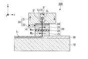
- a spin orbit torque wiring connected to the second ferromagnetic metal layer, The spin orbit torque wiring includes a pure spin current generation unit made of a material that generates a pure spin current, and a low resistance unit made of a material having an electric resistance smaller than that of the pure spin current generation unit. At least a part of the portion is in contact with the second ferromagnetic metal layer.
- the magnetoresistance effect element of the present invention it is possible to reduce the density of reversal current flowing through the magnetoresistance effect element.
- a wiring 30 for flowing a current in the stacking direction of the magnetoresistive effect element 20, a substrate 10 on which the wiring 30 is formed, and a cap layer are also shown.
- the stacking direction of the magnetoresistive effect element 20 is the z direction
- the direction perpendicular to the z direction and parallel to the spin orbit torque wiring 40 is the x direction
- the direction orthogonal to the x direction and the z direction is the y direction.
- the magnetoresistive element 20 is a tunneling magnetoresistance (TMR) element when the nonmagnetic layer 22 is made of an insulator, and a giant magnetoresistance (GMR) when the nonmagnetic layer 22 is made of metal. Giant Magnetoresistance) element.
- TMR tunneling magnetoresistance
- GMR giant magnetoresistance
- Heusler alloy such as Co 2 FeSi.
- the Heusler alloy includes an intermetallic compound having a chemical composition of X 2 YZ, where X is a transition metal element or noble metal element of Co, Fe, Ni, or Cu group on the periodic table, and Y is Mn, V It is a transition metal of Cr, Ti or Ti, and can take the elemental species of X, and Z is a typical element of Group III to Group V. Examples thereof include Co 2 FeSi, Co 2 MnSi, and Co 2 Mn 1-a Fe a Al b Si 1-b .
- the first ferromagnetic metal layer 21 has [Co (0.24 nm) / Pt (0.16 nm)] 6 / Ru (0.9 nm) / [Pt (0.16 nm) / Co (0.16 nm). )] 4 / Ta (0.2 nm) / FeB (1.0 nm).
- a ferromagnetic material particularly a soft magnetic material can be applied.
- a metal selected from the group consisting of Cr, Mn, Co, Fe, and Ni, an alloy containing one or more of these metals, these metals and at least one element of B, C, and N are included. Alloys that can be used can be used. Specific examples include Co—Fe, Co—Fe—B, and Ni—Fe.
- a known material can be used for the nonmagnetic layer 22.
- the nonmagnetic layer 22 is made of an insulator (when it is a tunnel barrier layer), as the material, Al 2 O 3 , SiO 2 , Mg, MgAl 2 O 4 O, or the like can be used.
- materials in which a part of Al, Si, Mg is substituted with Zn, Be, or the like can also be used.
- MgO and MgAl 2 O 4 are materials that can realize a coherent tunnel, spin can be injected efficiently.
- the nonmagnetic layer 22 is made of metal, Cu, Au, Ag, or the like can be used as the material.
- a cap layer 24 is preferably formed on the surface of the second ferromagnetic metal layer 23 opposite to the nonmagnetic layer 22 as shown in FIG.
- the cap layer 24 can suppress element diffusion from the second ferromagnetic metal layer 23.
- the cap layer 24 also contributes to the crystal orientation of each layer of the magnetoresistive effect element 20. As a result, by providing the cap layer 24, the magnetism of the first ferromagnetic metal layer 21 and the second ferromagnetic metal layer 23 of the magnetoresistive effect element 20 can be stabilized, and the resistance of the magnetoresistive effect element 20 can be reduced. it can.
- any one selected from the group consisting of silver, copper, magnesium, and aluminum for the cap layer 24.
- the cap layer 24 does not dissipate the spin propagating from the spin orbit torque wiring 40. It is known that silver, copper, magnesium, aluminum, and the like have a long spin diffusion length of 100 nm or more and are difficult to dissipate spin.
- the thickness of the cap layer 24 is preferably equal to or less than the spin diffusion length of the substance constituting the cap layer 24. If the thickness of the cap layer 24 is equal to or less than the spin diffusion length, the spin propagating from the spin orbit torque wiring 40 can be sufficiently transmitted to the magnetoresistive element 20.
- the upward spin S + (S1) and the downward spin S ⁇ (S2) are bent in directions orthogonal to the current, respectively.
- the normal Hall effect and the spin Hall effect are common in that the moving (moving) charge (electrons) can bend in the moving (moving) direction, but the normal Hall effect is that the charged particles moving in the magnetic field exert Lorentz force.
- the direction of motion is bent, but the spin Hall effect is greatly different in that the direction of movement is bent only by the movement of electrons (only the current flows) even though there is no magnetic field.
- the material of the spin orbit torque wiring does not include a material made only of a ferromagnetic material.
- the electron flow of the upward spin S + is defined as J ⁇
- the electron flow of the downward spin S ⁇ as J ⁇
- the spin current as J S
- J S J ⁇ ⁇ J ⁇
- JS flows upward in the figure as a pure spin current.
- J S is an electron flow having a polarizability of 100%.
- a current is passed through the spin orbit torque wiring to generate a pure spin current, and the pure spin current is diffused to the second ferromagnetic metal layer in contact with the spin orbit torque wiring.
- the spin orbit torque wiring 40 may include a nonmagnetic heavy metal.
- the heavy metal is used to mean a metal having a specific gravity equal to or higher than yttrium.
- the spin orbit torque wiring 40 may be made of only nonmagnetic heavy metal.
- the nonmagnetic heavy metal is preferably a nonmagnetic metal having an atomic number of 39 or more having d electrons or f electrons in the outermost shell. This is because such a nonmagnetic metal has a large spin-orbit interaction that causes a spin Hall effect.
- the spin orbit torque wiring 40 may be made of only a nonmagnetic metal having an atomic number of 39 or more and having d electrons or f electrons in the outermost shell.
- topological insulator for example, SnTe, Bi 1.5 Sb 0.5 Te 1.7 Se 1.3 , TlBiSe 2 , Bi 2 Te 3 , (Bi 1-x Sb x ) 2 Te 3 are preferable. These topological insulators can generate a spin current with high efficiency.
- a base layer (not shown) may be formed on the surface of the substrate 10 on the magnetoresistive effect element 20 side.
- the crystallinity such as crystal orientation and crystal grain size of each layer including the first ferromagnetic metal layer 21 laminated on the substrate 10 can be controlled.
- the underlayer preferably has an insulating property. This is to prevent current flowing in the wiring 30 and the like from being dissipated.
- Various layers can be used for the underlayer.
- the underlayer has a (001) -oriented NaCl structure and is at least one selected from the group consisting of Ti, Zr, Nb, V, Hf, Ta, Mo, W, B, Al, and Ce.
- a nitride layer containing two elements can be used.
- the wiring 30 is electrically connected to the first ferromagnetic metal layer 21 of the magnetoresistive effect element 20, and in FIG. 1, the wiring 30, the spin orbit torque wiring 40, and a power source (not shown) constitute a closed circuit. A current flows in the stacking direction of the magnetoresistive effect element 20.
- 3 to 6 are schematic views for explaining an embodiment of the spin orbit torque wiring, wherein (a) is a cross-sectional view and (b) is a plan view, respectively.
- the current that flows for the magnetization reversal of the magnetoresistive effect element of the present invention is the current that flows directly to the magnetoresistive effect element in order to use the STT effect (hereinafter referred to as “STT inversion current”
- STT inversion current the current that flows directly to the magnetoresistive effect element in order to use the STT effect
- SOT inversion current a current that flows through the spin orbit torque wiring in order to use the SOT effect. Since both currents are normal currents accompanied by the flow of electric charge, Joule heat is generated when the current is passed.
- the STT reversal current is reduced as compared with the configuration in which the magnetization reversal is performed only by the STT effect, but the energy of the SOT reversal current is reduced. Will consume.
- the spin orbit torque wiring has a portion with a small electric resistance rather than being made only of a material that can generate a pure spin current. That is, from this point of view, the spin orbit torque wiring includes a portion made of a material that generates a pure spin current (spin current generating portion), and a portion made of a material that has a lower electrical resistance than the spin current generating portion (low resistance portion). Preferably it consists of.
- the heavy metal does not form an alloy with the light metal, but the atoms of the heavy metal are randomly distributed in the light metal. Since the spin-orbit interaction is weak in light metals, a pure spin current is hardly generated by the spin Hall effect. However, when electrons pass through the heavy metal in the light metal, spin is scattered at the interface between the light metal and the heavy metal, so that a pure spin current can be efficiently generated even in a region where the concentration of heavy metal is low. If the concentration of heavy metal exceeds 50%, the proportion of the spin Hall effect in the heavy metal increases, but the effect at the interface between the light metal and heavy metal decreases, so the overall effect decreases. Therefore, the concentration of heavy metal is preferable so that a sufficient interface effect can be expected.
- the spin current generation portion in the spin orbit torque wiring can be made of an antiferromagnetic metal.
- the antiferromagnetic metal can obtain the same effect as the case of 100% nonmagnetic metal having an atomic number of 39 or more whose heavy metal has d electrons or f electrons in the outermost shell.
- the antiferromagnetic metal is preferably, for example, IrMn or PtMn, and more preferably IrMn that is stable against heat.
- the spin current generation unit in the spin orbit torque wiring can be made of a topological insulator.
- topological insulator for example, SnTe, Bi 1.5 Sb 0.5 Te 1.7 Se 1.3 , TlBiSe 2 , Bi 2 Te 3 , (Bi 1-x Sb x ) 2 Te 3 are preferable. These topological insulators can generate a spin current with high efficiency.
- the spin current generation unit In order for the pure spin current generated by the spin orbit torque wiring to effectively diffuse to the magnetoresistive effect element, at least a part of the spin current generation unit needs to be in contact with the second ferromagnetic metal layer. .
- the cap layer When the cap layer is provided, it is necessary that at least a part of the spin current generator is in contact with the cap layer. In all the embodiments of the spin orbit torque wiring shown in FIGS. 3 to 6, at least a part of the spin current generator is in contact with the second ferromagnetic metal layer.
- the junction 40 ′ with the second ferromagnetic metal layer is entirely composed of the spin current generator 41, and the spin current generator 41 is connected to the low resistance parts 42A and 42B. It is a sandwiched configuration.
- the spin current generation unit 41 is superimposed on a part of the junction 23 ′ of the second ferromagnetic metal layer 23 in plan view from the stacking direction of the magnetoresistive effect element 20.
- the thickness direction includes only the spin current generation unit 41, and the low resistance portions 42A and 42B are arranged so as to sandwich the spin current generation unit 41 in the direction of current flow.
- the spin orbit torque wiring 40 shown in FIG. 5 is superimposed so that the spin current generation part 41 includes the junction part 23 ′ of the second ferromagnetic metal layer 23 in plan view from the stacking direction of the magnetoresistive effect element 20,
- the spin current generation unit 41 and the low resistance unit 42C are sequentially stacked from the second ferromagnetic metal layer side, and the low resistance units 42A and 42B are stacked in the direction of current flow.
- the resistor portions 42C are arranged so as to sandwich the portion where the resistor portions 42C are stacked.
- the second spin current generator is superposed so as to overlap the junction of the second ferromagnetic metal layer in plan view from the stacking direction of the magnetoresistive effect element, and the others Has the same configuration as the spin orbit torque wiring shown in FIG.
- the nonmagnetic metal since the area where the spin current generation unit 41 and the low resistance unit 42 are in contact with each other is wide, the nonmagnetic metal having a large atomic number that forms the spin current generation unit 41 and the metal that configures the low resistance unit 42 High adhesion.
- the magnetoresistive effect element of the present invention can be manufactured using a known method. A method for manufacturing the magnetoresistive effect element shown in FIGS. 3 to 6 will be described below.
- the magnetoresistive element 20 can be formed using, for example, a magnetron sputtering apparatus.
- the tunnel barrier layer is initially about 0.4 to 2.0 nm of aluminum on the first ferromagnetic metal layer, and divalent cations of a plurality of nonmagnetic elements.
- the metal thin film to be formed is sputtered and subjected to natural oxidation by plasma oxidation or oxygen introduction, followed by heat treatment.
- a thin film forming method in addition to a magnetron sputtering method, a thin film forming method such as a vapor deposition method, a laser ablation method, or an MBE method can be used.
- a thin film forming method such as a vapor deposition method, a laser ablation method, or an MBE method.
- the spin current generator 41 After forming the magnetoresistive effect element 20 and forming the shape, it is preferable to form the spin current generator 41 first. This is because a structure that can suppress the scattering of pure spin current from the spin current generator 41 to the magnetoresistive element 20 as much as possible leads to high efficiency.
- the periphery of the processed magnetoresistive effect element 20 is filled with a resist or the like to form a surface including the upper surface of the magnetoresistive effect element 20.
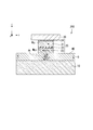
- FIG. 7 is a schematic cross-sectional view of the magnetoresistive effect element according to one embodiment of the present invention cut along a yz plane. Based on FIG. 7, an operation of the magnetoresistive element 100 according to one embodiment of the present invention will be described.
- the current I 2 corresponds to the current I shown in FIG.
- the upward spin S + and the downward spin S ⁇ are bent toward the end of the spin orbit torque wiring 40 to generate a pure spin current J s .
- the pure spin current J s is induced in a direction perpendicular to the direction in which the current I 2 flows. That is, a pure spin current Js is generated in the z-axis direction and the x-axis direction in the figure.
- FIG. 7 only the pure spin current J s in the z-axis direction that contributes to the magnetization direction of the second ferromagnetic metal layer 23 is illustrated.
- the magnetization M 23 of the second ferromagnetic metal layer 23 is affected. That is, in FIG. 7, the torque that attempts to cause the magnetization reversal of the magnetization M 23 of the second ferromagnetic metal layer 23 oriented in the + x direction by the spin directed in the ⁇ x direction flowing into the second ferromagnetic metal layer 23. (SOT) is added.
- the SOT effect caused by the pure spin current J s generated by the current flowing through the second current path I 2 is added to the STT effect generated by the current flowing through the first current path I 1 , and the second ferromagnetic metal layer 23. the magnetization M 23 to the magnetization reversal of.
- the magnetization of the second ferromagnetic metal layer 23 is to be reversed only by the STT effect (that is, a current flows only in the current I 1 ), it is necessary to apply a voltage higher than a predetermined voltage to the magnetoresistive effect element 20.
- a general drive voltage of a TMR element is relatively small, such as several volts or less, but the nonmagnetic layer 22 is a very thin film of about several nm, and dielectric breakdown may occur. By continuing energization of the nonmagnetic layer 22, a weak portion of the nonmagnetic layer (film quality is poor, film thickness is thin, etc.) is destroyed.
- the current density of the current flowing through the spin orbit torque wiring is preferably less than 1 ⁇ 10 7 A / cm 2 . If the current density of the current flowing through the spin orbit torque wiring is too large, heat is generated by the current flowing through the spin orbit torque wiring. When heat is applied to the second ferromagnetic metal layer, the magnetization stability of the second ferromagnetic metal layer is lost, and unexpected magnetization reversal may occur. When such unexpected magnetization reversal occurs, there arises a problem that recorded information is rewritten. That is, in order to avoid unexpected magnetization reversal, it is preferable that the current density of the current flowing through the spin orbit torque wiring is not excessively increased. If the current density of the current flowing through the spin orbit torque wiring is less than 1 ⁇ 10 7 A / cm 2 , it is possible to avoid at least magnetization reversal caused by generated heat.
- FIG. 8 shows a magnetoresistive element according to another embodiment of the present invention.
- the spin orbit torque wiring 50 has a second strong strength in addition to the upper surface joint portion 51 (corresponding to the spin orbit torque wiring 40 described above) provided in the stacking direction of the magnetoresistive effect element 20.
- Side wall joints 52 that join the side walls of the magnetic metal layer 23 are provided.
- FIG. 9 shows a magnetoresistive effect element according to another embodiment of the present invention.
- the magnetoresistive effect element 300 shown in FIG. 9 has a spin orbit torque wiring 40 on the substrate 10 side.
- the stacking order of the first ferromagnetic metal layer 23 that is a fixed layer and the second ferromagnetic metal layer 24 that is a free layer is opposite to that of the magnetoresistive element 100 shown in FIG.
- the magnetoresistive element of the present invention may have a top pin structure as in this configuration, or may have a bottom pin structure as shown in FIG.
- the substrate 10, the spin orbit torque wiring 40, the second ferromagnetic metal layer 23, the nonmagnetic layer 22, the first ferromagnetic metal layer 21, the cap layer 24, and the wiring 30 are arranged in this order. Laminated. Since the second ferromagnetic metal layer 23 is laminated before the first ferromagnetic metal layer 21, the second ferromagnetic metal layer 23 is less likely to be affected by lattice distortion or the like than the magnetoresistive effect element 100. As a result, in the magnetoresistive effect element 300, the perpendicular magnetic anisotropy of the second ferromagnetic metal layer 23 is increased. When the perpendicular magnetic anisotropy of the second ferromagnetic metal layer 23 increases, the MR ratio of the magnetoresistive element can be increased.
- FIG. 10 shows a first power supply 110 for supplying current in the stacking direction of the magnetoresistive effect element 20 and a second power supply 120 for supplying current to the spin orbit torque wiring 40 in the magnetoresistive effect element 100 shown in FIG. It is a thing.
- the first power supply 110 is connected to the wiring 30 and the spin orbit torque wiring 40.
- the first power source 110 can control the current flowing in the stacking direction of the magnetoresistive effect element 100.
- the second power source 120 is connected to both ends of the spin orbit torque wiring 40.
- the second power supply 120 can control the current flowing in the spin orbit torque wiring 40 that is a current flowing in a direction orthogonal to the stacking direction of the magnetoresistive effect element 20.
- the current flowing in the stacking direction of the magnetoresistive effect element 20 induces STT.
- the current flowing through the spin orbit torque wiring 40 induces SOT. Both STT and SOT contribute to the magnetization reversal of the second ferromagnetic metal layer 23.
- the contribution ratio of SOT and STT contributing to the magnetization reversal is free. Can be controlled.
- the amount of current flowing from the first power source 110 can be increased, and the amount of current flowing from the second power source 120 can be reduced.
- the amount of current flowing from the first power source 110 can be reduced, the amount of current flowing from the second power source 120 can be increased, and the contribution rate of SOT can be increased.
- a well-known thing can be used for the 1st power supply 110 and the 2nd power supply 120.
- the contribution ratios of STT and SOT can be freely controlled by the amount of current supplied from the first power supply and the second power supply. Therefore, the contribution ratio of STT and SOT can be freely controlled according to the performance required for the device, and it can function as a more versatile magnetoresistive element.
- Magnetic memory The magnetic memory (MRAM) of the present invention includes a plurality of magnetoresistive elements of the present invention.
- the magnetization reversal method according to an aspect of the present invention is such that the current density flowing through the spin orbit torque wiring is less than 1 ⁇ 10 7 A / cm 2 in the magnetoresistive effect element of the present invention. If the current density of the current flowing through the spin orbit torque wiring is too large, heat is generated by the current flowing through the spin orbit torque wiring. When heat is applied to the second ferromagnetic metal layer, the magnetization stability of the second ferromagnetic metal layer is lost, and unexpected magnetization reversal may occur. When such unexpected magnetization reversal occurs, there arises a problem that recorded information is rewritten.
- the current density of the current flowing through the spin orbit torque wiring is not excessively increased. If the current density of the current flowing through the spin orbit torque wiring is less than 1 ⁇ 10 7 A / cm 2 , it is possible to avoid at least magnetization reversal caused by generated heat.
- the magnetization reversal method is a method of applying a current to a power source of a magnetoresistive effect element after applying a current to a power source of a spin orbit torque wiring in the magnetoresistive effect element of the present invention.
- the assist process and the magnetization reversal process may be performed simultaneously, or after the assist process is performed in advance, the magnetization reversal process may be added. That is, in the magnetoresistive effect element 200 shown in FIG. 7, the current may be supplied simultaneously from the first power source 110 and the second power source 120, or after the current is supplied from the second current 120, the first power source 110 is added.
- the current is supplied to the power source of the magnetoresistive effect element. It is preferable to apply. That is, it is preferable to supply current from the first power source 110 after supplying current from the second current 120.
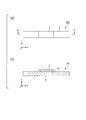
- FIG. 11 shows a schematic diagram of an example of a spin current magnetization switching element according to an embodiment of the present invention.
- 11A is a plan view
- FIG. 11B is a cross-sectional view taken along the line XX which is the center line in the width direction of the spin orbit torque wiring 2 of FIG. 11A.
- the spin current magnetization reversal element 101 according to one embodiment of the present invention is different from the spin current magnetization reversal element 101 shown in FIG. 1 in that the surface of the second ferromagnetic metal layer 1 and the second ferromagnetic metal layer 1 whose magnetization direction is variable.
- a spin orbit torque wiring 2 extending in a second direction (x direction) intersecting the first direction (z direction) which is a straight direction and joining to the first surface 1a of the second ferromagnetic metal layer 1; Is provided.
- the spin orbit torque wiring 2 and the second ferromagnetic metal layer 1 may be joined “directly” or “via another layer” such as a cap layer as described above. If the configuration is such that the pure spin current generated in the spin orbit torque wiring 2 flows into the second ferromagnetic metal layer 1, the junction (connection or coupling) between the spin orbit torque wiring and the first ferromagnetic metal layer is possible. There is no limit to how.
- the spin orbit torque wiring 2 includes a pure spin current generator 2A made of a material that generates a pure spin current, and a low resistance part 2B made of a material having a smaller electrical resistance than the pure spin current generator.
- a pure spin current generator 2A made of a material that generates a pure spin current
- a low resistance part 2B made of a material having a smaller electrical resistance than the pure spin current generator.
- at least a part of the pure spin current generator can be in contact with the second ferromagnetic metal layer 1.
- the configuration shown in FIG. 12 is an example in which the configuration of the spin orbit torque wiring shown in FIG. 3 is applied to the spin current magnetization switching element of the present invention.
- the configuration of the spin orbit torque wiring shown in FIGS. 4 to 6 can be applied to the spin current magnetization switching element of the present invention.
- a magnetoresistive effect element can be mainly mentioned. Therefore, in the constituent elements included in the spin current magnetization reversal element of the present invention, all the equivalent constituent elements such as the above-described magnetoresistive effect element can be applied.
- the application of the spin current magnetization reversal element of the present invention is not limited to the magnetoresistive effect element, and can be applied to other applications.
- Other applications include, for example, a spatial light modulator that spatially modulates incident light using a magneto-optic effect by arranging a spin current magnetization reversal element in each pixel,
- the magnetic field applied to the easy axis of the magnet may be replaced with a spin current magnetization reversal element.
- Magnetoresistance effect element 101 ... Spin current magnetization reversal element, I ... current, S1 ... up spin, S2 ... down spin, M 21, M 23 ... magnetization, I 1 ... first current path, I 2 ... second current path, 110 ... first power supply, 120 ... second Power supply
Landscapes
- Engineering & Computer Science (AREA)
- Computer Hardware Design (AREA)
- Crystallography & Structural Chemistry (AREA)
- Power Engineering (AREA)
- Chemical & Material Sciences (AREA)
- Physics & Mathematics (AREA)
- Manufacturing & Machinery (AREA)
- General Physics & Mathematics (AREA)
- General Engineering & Computer Science (AREA)
- Theoretical Computer Science (AREA)
- Software Systems (AREA)
- Condensed Matter Physics & Semiconductors (AREA)
- Computer Security & Cryptography (AREA)
- Hall/Mr Elements (AREA)
- Mram Or Spin Memory Techniques (AREA)
Abstract
Description
本願は、2015年11月27日に、日本に出願された特願2015-232334号、2016年3月16日に、日本に出願された特願2016-53072号、2016年3月18日に、日本に出願された特願2016-56058号、2016年10月27日に、日本に出願された特願2016-210531号、2016年10月27日に、日本に出願された特願2016-210533号に基づき優先権を主張し、その内容をここに援用する。
磁場を利用する方式では、素子サイズが小さくなると、細い配線に流すことができる電流では書き込みができなくなるという問題がある。
これに対して、スピントランスファートルク(STT)を利用する方式では、一方の強磁性層(固定層、参照層)が電流をスピン分極させ、その電流のスピンがもう一方の強磁性層(自由層、記録層)の磁化に移行され、その際に生じるトルク(STT)によって書き込み(磁化反転)が行われるが、素子サイズが小さくなるほど書き込みに必要な電流が小さくて済むという利点がある。
TMR素子の長寿命の観点からはこの反転電流密度は低いことが望ましい。この点は、GMR素子についても同様である。
従って、TMR素子及びGMR素子のいずれの磁気抵抗効果素子においても、この磁気抵抗効果素子に流れる電流密度を低減することが望まれる。
前記スピン軌道トルク配線は、純スピン流を生成する材料からなる純スピン流生成部と、該純スピン流生成部よりも電気抵抗が小さい材料からなる低抵抗部とからなり、該純スピン流生成部の少なくとも一部が前記第2強磁性金属層と接している。
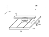
図1は、本発明の一態様に係る磁気抵抗効果素子を模式的に示した斜視図である。
本発明の一態様に係る磁気抵抗効果素子100は、磁気抵抗効果素子20と、該磁気抵抗効果素子20の積層方向に対して交差する方向に延在し、磁気抵抗効果素子20に接合するスピン軌道トルク配線40とを有する。
図1を含めて以下では、スピン軌道トルク配線が磁気抵抗効果素子の積層方向に対して交差する方向に延在する構成の例として、直交する方向に延在する構成の場合について説明する。
図1においては、磁気抵抗効果素子20の積層方向に電流を流すための配線30と、その配線30を形成する基板10と、キャップ層も示している。
以下、磁気抵抗効果素子20の積層方向をz方向、z方向と垂直でスピン軌道トルク配線40と平行な方向をx方向、x方向及びz方向と直交する方向をy方向とする。
磁気抵抗効果素子20は、磁化の向きが固定された第1強磁性金属層21と、磁化の向きが可変な第2強磁性金属層23と、第1強磁性金属層21及び第2強磁性金属層23に挟持された非磁性層22とを有する。
第1強磁性金属層21の磁化が一方向に固定され、第2強磁性金属層23の磁化の向きが相対的に変化することで、磁気抵抗効果素子20として機能する。保磁力差型(擬似スピンバルブ型;Pseudo spin valve 型)のMRAMに適用する場合には、第1強磁性金属層の保持力は第2強磁性金属層の保磁力よりも大きいものであり、また、交換バイアス型(スピンバルブ;spin valve型)のMRAMに適用する場合には、第1強磁性金属層では反強磁性層との交換結合によって磁化の向きが固定される。
また、磁気抵抗効果素子20は、非磁性層22が絶縁体からなる場合は、トンネル磁気抵抗(TMR:Tunneling Magnetoresistance)素子であり、非磁性層22が金属からなる場合は巨大磁気抵抗(GMR:Giant Magnetoresistance)素子である。
第1強磁性金属層21は固定層や参照層、第2強磁性金属層23は自由層や記憶層などと呼ばれる。
例えば、非磁性層22が絶縁体からなる場合(トンネルバリア層である場合)、その材料としては、Al2O3、SiO2、Mg、及び、MgAl2O4O等を用いることができる。またこれらの他にも、Al,Si,Mgの一部が、Zn、Be等に置換された材料等も用いることができる。これらの中でも、MgOやMgAl2O4はコヒーレントトンネルが実現できる材料であるため、スピンを効率よく注入できる。
また、非磁性層22が金属からなる場合、その材料としては、Cu、Au、Ag等を用いることができる。
スピン軌道トルク配線は、磁気抵抗効果素子の積層方向に対して交差する方向に延在する。スピン軌道トルク配線は、該スピン軌道トルク配線に磁気抵抗効果素子の積層方向に対して直交する方向に電流を流す電源に電気的に接続され、その電源と共に、磁気抵抗効果素子に純スピン流を注入するスピン注入手段として機能する。
スピン軌道トルク配線40は、第2強磁性金属層23に直接接続されていてもよいし、他の層を介して例えば、図1に示すようにキャップ層24を介して接続されていてもよい。
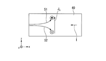
スピンホール効果とは、材料に電流を流した場合にスピン軌道相互作用に基づき、電流の向きに直交する方向に純スピン流が誘起される現象である。
非磁性体(強磁性体ではない材料)では上向きスピンS+の電子数と下向きスピンS-の電子数とが等しいので、図中で上方向に向かう上向きスピンS+の電子数と下方向に向かう下向きスピンS-の電子数が等しい。そのため、電荷の正味の流れとしての電流はゼロである。この電流を伴わないスピン流は特に純スピン流と呼ばれる。
これに対して、強磁性体中に電流を流した場合にも上向きスピン電子と下向きスピン電子が互いに反対方向に曲げられる点は同じであるが、強磁性体中では上向きスピン電子と下向きスピン電子のいずれかが多い状態であるため、結果として電荷の正味の流れが生じてしまう(電圧が発生してしまう)点で異なる。従って、スピン軌道トルク配線の材料としては、強磁性体だけからなる材料は含まれない。
図2において、スピン軌道トルク配線40の上面に強磁性体を接触させると、純スピン流は強磁性体中に拡散して流れ込むことになる。
本発明では、このようにスピン軌道トルク配線に電流を流して純スピン流を生成し、その純スピン流がスピン軌道トルク配線に接する第2強磁性金属層に拡散する構成とすることで、従来のSTTを利用する磁気抵抗効果素子において強磁性金属層の磁化反転のアシスト手段あるいは主力手段として用いることもできるし、純スピン流によるSOTのみで強磁性金属層の磁化反転を行う新規の磁気抵抗効果素子において用いることもできる。。
この場合、非磁性の重金属は最外殻にd電子又はf電子を有する原子番号39以上の原子番号が大きい非磁性金属であることが好ましい。かかる非磁性金属は、スピンホール効果を生じさせるスピン軌道相互作用が大きいからである。スピン軌道トルク配線40は、最外殻にd電子又はf電子を有する原子番号39以上の原子番号が大きい非磁性金属だけからなってもよい。
通常、金属に電流を流すとすべての電子はそのスピンの向きに関わりなく、電流とは逆向きに動くのに対して、最外殻にd電子又はf電子を有する原子番号が大きい非磁性金属はスピン軌道相互作用が大きいためにスピンホール効果によって電子の動く方向が電子のスピンの向きに依存し、純スピン流JSが発生しやすい。
スピン軌道相互作用はスピン軌道トルク配線材料の物質の固有の内場によって生じるため、非磁性材料でも純スピン流が生じる。スピン軌道トルク配線材料に微量の磁性金属を添加すると、磁性金属自体が流れる電子スピンを散乱するためにスピン流生成効率が向上する。ただし、磁性金属の添加量が増大し過ぎると、発生した純スピン流が添加された磁性金属によって散乱されるため、結果としてスピン流が減少する作用が強くなる。したがって、添加される磁性金属のモル比はスピン軌道トルク配線における純スピン生成部の主成分のモル比よりも十分小さい方が好ましい。目安で言えば、添加される磁性金属のモル比は3%以下であることが好ましい。
トポロジカル絶縁体としては例えば、SnTe,Bi1.5Sb0.5Te1.7Se1.3,TlBiSe2,Bi2Te3,(Bi1-xSbx)2Te3などが好ましい。これらのトポロジカル絶縁体は、高効率でスピン流を生成することが可能である。
基板10は、平坦性に優れることが好ましい。平坦性に優れた表面を得るために、材料として例えば、Si、AlTiC等を用いることができる。
例えば1つの例として、下地層には(001)配向したNaCl構造を有し、Ti,Zr,Nb,V,Hf,Ta,Mo,W,B,Al,Ceの群から選択される少なくとも1つの元素を含む窒化物の層を用いることができる。
配線30は、磁気抵抗効果素子20の第1強磁性金属層21に電気的に接続され、図1においては、配線30とスピン軌道トルク配線40と電源(図示略)とで閉回路を構成し、磁気抵抗効果素子20の積層方向に電流が流される。
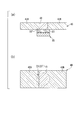
図3~図6に示すスピン軌道トルク配線の実施形態は、上述の材料以外の構成によって、SOT反転電流によるジュール熱を低減する構成の例である。
この構成においては、STT効果による磁化反転とSOT効果による磁化反転を併用するため、STT効果だけで磁化反転を行う構成に比べてSTT反転電流は低減されるが、SOT反転電流の分のエネルギーを消費することになる。
そのため、SOT反転電流によるジュール熱を低減する観点では、スピン軌道トルク配線はすべてが純スピン流を生成しうる材料だけからなるよりも、電気抵抗が小さい部分を有することが好ましい。すなわち、この観点では、スピン軌道トルク配線は純スピン流を生成する材料からなる部分(スピン流生成部)と、このスピン流生成部よりも電気抵抗が小さい材料からなる部分(低抵抗部)とからなるのが好ましい。
低抵抗部は、通常の配線として用いられる材料を用いることができる。例えば、アルミニウム、銀、銅、金等を用いることができる。低抵抗部は、スピン流生成部よりも電気抵抗が小さい材料からなっていればよく、例えば、複数種類の材料部分からなる構成等であってもよい。
なお、低抵抗部において純スピン流が生成されても構わない。この場合、スピン流生成部と低抵抗部との区別は、本明細書中にスピン流生成部及び低抵抗部の材料として記載したものからなる部分はスピン流生成部または低抵抗部であるとして区別できる。また、純スピン流を生成する主要部以外の部分であって、その主要部より電気抵抗が小さい部分は低抵抗部として、スピン流生成部と区別できる。
ここで、スピン流生成部の主成分よりも純スピン流を生成しうる重金属が十分少ない濃度領域とは、例えば、銅を主成分とするスピン流生成部において、モル比で重金属の濃度が10%以下を指す。スピン流生成部を構成する主成分が上述の重金属以外からなる場合、スピン流生成部に含まれる重金属の濃度はモル比で50%以下であることが好ましく、10%以下であることがさらに好ましい。これらの濃度領域は、電子のスピン散乱の効果が有効に得られる領域である。重金属の濃度が低い場合、重金属よりも原子番号が小さい軽金属が主成分となる。なお、この場合、重金属は軽金属との合金を形成しているのではなく、軽金属中に重金属の原子が無秩序に分散していることを想定している。軽金属中ではスピン軌道相互作用が弱いため、スピンホール効果によって純スピン流は生成しにくい。しかしながら、電子が軽金属中の重金属を通過する際に、軽金属と重金属の界面でもスピンが散乱される効果があるため重金属の濃度が低い領域でも純スピン流が効率よく発生させることが可能である。重金属の濃度が50%を超えると、重金属中のスピンホール効果の割合は大きくなるが、軽金属と重金属の界面の効果が低下するため総合的な効果が減少する。したがって、十分な界面の効果が期待できる程度の重金属の濃度が好ましい。
また、上述のスピン軌道トルク配線がトポロジカル絶縁体を含む場合、スピン軌道トルク配線におけるスピン流生成部をトポロジカル絶縁体からなるものとすることができる。トポロジカル絶縁体としては例えば、SnTe,Bi1.5Sb0.5Te1.7Se1.3,TlBiSe2,Bi2Te3,(Bi1-xSbx)2Te3などが好ましい。これらのトポロジカル絶縁体は高効率でスピン流を生成することが可能である。
SOT反転電流に対する純スピン流生成効率の観点で、スピン軌道トルク配線に流れる電流がすべてスピン流生成部を流れるようにするためには、スピン流生成部と低抵抗部とが電気的に並列に配置する部分がなく、すべて電気的に直列に配置するようにする。
図3~図6に示すスピン軌道トルク配線は、磁気抵抗効果素子の積層方向からの平面視で、スピン流生成部と低抵抗部とが電気的に並列に配置する部分がない構成であり、(a)で示す断面を有する構成の中で、SOT反転電流に対する純スピン流生成効率が最も高い構成の場合である。
図6に示す構成では、スピン流生成部41と低抵抗部42とが接する面積が広いため、スピン流生成部41を構成する原子番号の大きい非磁性金属と低抵抗部42を構成する金属との密着性が高い。
まず、磁気抵抗効果素子20例えば、マグネトロンスパッタ装置を用いて形成することができる。磁気抵抗効果素子20がTMR素子の場合、例えば、トンネルバリア層は第1強磁性金属層上に最初に0.4~2.0nm程度のアルミニウム、及び複数の非磁性元素の二価の陽イオンとなる金属薄膜をスパッタし、プラズマ酸化あるいは酸素導入による自然酸化を行い、その後の熱処理によって形成される。成膜法としてはマグネトロンスパッタ法のほか、蒸着法、レーザアブレーション法、MBE法等の薄膜作成法を用いることができる。
磁気抵抗効果素子20の成膜及び形状の形成を行った後、スピン流生成部41を最初に形成することが好ましい。これはスピン流生成部41から磁気抵抗効果素子20に純スピン流の散乱をできるだけ抑制できる構造にすることが高効率化に繋がるからである。
磁気抵抗効果素子20の成膜及び形状の形成を行った後、加工後の磁気抵抗効果素子20の周囲をレジスト等で埋めて、磁気抵抗効果素子20の上面を含む面を形成する。この際、磁気抵抗効果素子20の上面を平坦化することが好ましい。平坦化することで、スピン流生成部41と磁気抵抗効果素子20の界面におけるスピン散乱を抑制することができる。
次に、平坦化した磁気抵抗効果素子20の上面にスピン流生成部41の材料を成膜する。成膜はスパッタ等を用いることができる。
次に、スピン流生成部41を作製したい部分にレジストまたは保護膜を設置し、イオンミリング法または反応性イオンエッチング(RIE)法を用いて不要部を除去する。
次に、低抵抗部42を構成する材料をスパッタ等で成膜し、レジスト等を剥離することで、スピン軌道トルク配線40が作製される。スピン流生成部41の形状が複雑な場合は、レジストまたは保護膜の形成と、スピン流生成部41の成膜を複数回に分けて形成してもよい。
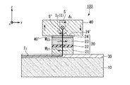
図7に基づいて、本発明の一態様に係る磁気抵抗効果素子100の作用について説明する。
もう一つは、スピン軌道トルク配線40の延在方向に流れる電流I2(SOT反転電流)である。
電流I1と電流I2とは互いに交差(直交)するものであり、磁気抵抗効果素子20とスピン軌道トルク配線40とが接合する部分(符号24’は磁気抵抗効果素子20(キャップ層24)側の接合部を示し、符号40’はスピン軌道トルク配線40側の接合部を示す)において、磁気抵抗効果素子20に流れる電流とスピン軌道トルク配線40に流れる電流が合流し、または、分配される。
図8に示す磁気抵抗効果素子200において、スピン軌道トルク配線50は磁気抵抗効果素子20の積層方向に備えた上面接合部51(上述のスピン軌道トルク配線40に相当)の他に、第2強磁性金属層23の側壁に接合する側壁接合部52を有する。
従って、純スピン流Jsが磁気抵抗効果素子20の上面からキャップ層24を介して第2強磁性金属層23に流れ込むだけでなく、純スピン流Js’が第2強磁性金属層23の側壁から流れ込むので、SOT効果が増強される。
図9に示す磁気抵抗効果素子300では、基板10側にスピン軌道トルク配線40を有する。この場合、固定層である第1強磁性金属層23と自由層である第2強磁性金属層24の積層順が図1に示す磁気抵抗効果素子100とは逆になる。
このように、本発明の磁気抵抗効果素子は、この構成のようにトップピン構造であってもよいし、図1に示したようなボトムピン構造であってもよい。
第2電源120は、スピン軌道トルク配線40の両端に接続されている。第2電源120は、磁気抵抗効果素子20の積層方向に対して直交する方向に流れる電流である、スピン軌道トルク配線40に流れる電流を制御することができる。
また、例えば薄いデバイスを作製する必要があり、非磁性層22の厚みを薄くせざる得ない場合は、非磁性層22に流れる電流を少なくことが求められる。この場合は、第1電源110から流れる電流量を少なくし、第2電源120から流れる電流量を多くし、SOTの寄与率を高めることができる。
本発明の磁気メモリ(MRAM)は、本発明の磁気抵抗効果素子を複数備える。
本発明の一態様に係る磁化反転方法は、本発明の磁気抵抗効果素子において、スピン軌道トルク配線に流れる電流密度が1×10⁷A/cm2未満とするものである。
スピン軌道トルク配線に流す電流の電流密度が大きすぎると、スピン軌道トルク配線に流れる電流によって熱が生じる。熱が第2強磁性金属層に加わると、第2強磁性金属層の磁化の安定性が失われ、想定外の磁化反転等が生じる場合がある。このような想定外の磁化反転が生じると、記録した情報が書き換わるという問題が生じる。すなわち、想定外の磁化反転を避けるためには、スピン軌道トルク配線に流す電流の電流密度が大きくなりすぎないようにすることが好ましい。スピン軌道トルク配線に流す電流の電流密度は1×10⁷A/cm2未満であれば、少なくとも発生する熱により磁化反転が生じることを避けることができる。
アシスト工程と磁化反転工程は、同時に行ってもよいし、アシスト工程を事前に行った後に磁化反転工程を加えて行ってもよい。すなわち、図7に示す磁気抵抗効果素子200においては、第1電源110と第2電源120から電流を同時に供給してもよいし、第2電流120から電流を供給後に、加えて第1電源110から電流を供給してもよいが、SOTを利用した磁化反転のアシスト効果をより確実に得るためには、スピン軌道トルク配線の電源に電流が印加した後に、磁気抵抗効果素子の電源に電流を印加することが好ましい。すなわち、第2電流120から電流を供給後に、加えて第1電源110から電流を供給することが好ましい。
図11に、本発明の一実施形態に係るスピン流磁化反転素子の一例の模式図を示す。図11(a)は平面図であり、図11(b)は図11(a)のスピン軌道トルク配線2の幅方向の中心線であるX-X線で切った断面図である。
本発明の一態様に係るスピン流磁化反転素子は、図1に示すスピン流磁化反転素子101は、磁化の向きが可変な第2強磁性金属層1と、第2強磁性金属層1の面直方向である第1方向(z方向)に対して交差する第2方向(x方向)に延在し、第2強磁性金属層1の第1面1aに接合するスピン軌道トルク配線2と、を備える。
ここで、スピン軌道トルク配線2と第2強磁性金属層1との接合は、「直接」接合してもよいし、上述したようにキャップ層のような「他の層を介して」接合してもよく、スピン軌道トルク配線2で発生した純スピン流が第2強磁性金属層1に流れ込む構成であれば、スピン軌道トルク配線と第1強磁性金属層との接合(接続あるいは結合)の仕方に限定はない。
図12に示す構成は、図3に示したスピン軌道トルク配線の構成を本発明のスピン流磁化反転素子に適用した例である。本発明のスピン流磁化反転素子に図4~図6に示したスピン軌道トルク配線の構成を適用することができる。
Claims (10)
- 磁化の向きが固定された第1強磁性金属層と、磁化の向きが可変な第2強磁性金属層と、第1強磁性金属層及び第2強磁性金属層に挟持された非磁性層とを有する磁気抵抗効果素子と、
該磁気抵抗効果素子の積層方向に対して交差する方向に延在し、前記第2強磁性金属層に接合するスピン軌道トルク配線と、を備え、
前記磁気抵抗効果素子と前記スピン軌道トルク配線とが接合する部分において、前記磁気抵抗効果素子に流れる電流と前記スピン軌道トルク配線に流れる電流が合流し、または、分配される磁気抵抗効果素子。 - 前記スピン軌道トルク配線は、最外殻にd電子又はf電子を有する原子番号39以上の非磁性金属を含む請求項1に記載の磁気抵抗効果素子。
- 前記スピン軌道トルク配線は、純スピン流を生成する材料からなる純スピン流生成部と、該純スピン流生成部よりも電気抵抗が小さい材料からなる低抵抗部とからなり、該純スピン流生成部の少なくとも一部が前記第2強磁性金属層と接している請求項1又は2のいずれかに記載の磁気抵抗効果素子。
- 前記スピン軌道トルク配線は、磁性金属を含む請求項1~3のいずれか一項に記載の磁気抵抗効果素子。
- 前記スピン軌道トルク配線と前記第2強磁性金属層との間にキャップ層を有し、前記スピン軌道トルク配線と前記第2強磁性金属層とは前記キャップ層を介して接合されている請求項1~4のいずれか一項に記載の磁気抵抗効果素子。
- 前記スピン軌道トルク配線は、前記第2強磁性金属層の側壁に接合する側壁接合部を有する請求項1~5のいずれか一項に記載の磁気抵抗効果素子。
- 請求項1~6のいずれか一項に記載の磁気抵抗効果素子を複数備えた磁気メモリ。
- 前記スピン軌道トルク配線に流れる電流密度が1×10⁷A/cm2未満とすることを特徴とする請求項1~6に記載の磁気抵抗効果素子における磁化反転方法。
- 前記スピン軌道トルク配線の電源に電流を印加した後に、前記磁気抵抗効果素子の電源に電流を印加することを特徴とする請求項1~6に記載の磁気抵抗効果素子における磁化反転方法。
- 磁化の向きが可変な第2強磁性金属層と、
前記第2強磁性金属層の面直方向に対して交差する方向に延在し、前記第2強磁性金属層に接合するスピン軌道トルク配線と、を備え、
前記スピン軌道トルク配線は、純スピン流を生成する材料からなる純スピン流生成部と、該純スピン流生成部よりも電気抵抗が小さい材料からなる低抵抗部とからなり、該純スピン流生成部の少なくとも一部が前記第2強磁性金属層と接しているスピン流磁化反転素子。
Priority Applications (10)
| Application Number | Priority Date | Filing Date | Title |
|---|---|---|---|
| CN202210022833.2A CN114361329A (zh) | 2015-11-27 | 2016-11-25 | 磁阻效应元件、磁存储器、磁化反转方法及自旋流磁化反转元件 |
| US15/777,894 US10510948B2 (en) | 2015-11-27 | 2016-11-25 | Magnetoresistive effect element, magnetic memory, magnetization rotation method, and spin current magnetization rotational element |
| CN201680068515.2A CN108292702B (zh) | 2015-11-27 | 2016-11-25 | 磁阻效应元件、磁存储器、磁化反转方法及自旋流磁化反转元件 |
| JP2017552731A JP6621839B2 (ja) | 2015-11-27 | 2016-11-25 | 磁気抵抗効果素子、磁気メモリ、磁化反転方法、及び、スピン流磁化反転素子 |
| US16/671,567 US10964885B2 (en) | 2015-11-27 | 2019-11-01 | Magnetoresistive effect element, magnetic memory, magnetization rotation method, and spin current magnetization rotational element |
| US17/184,206 US11355698B2 (en) | 2015-11-27 | 2021-02-24 | Magnetoresistive effect element, magnetic memory, magnetization rotation method, and spin current magnetization rotational element |
| US17/715,477 US11637237B2 (en) | 2015-11-27 | 2022-04-07 | Spin current magnetization rotational element |
| US18/167,325 US12096699B2 (en) | 2015-11-27 | 2023-02-10 | Magnetoresistive effect element |
| US18/397,344 US20240130247A1 (en) | 2015-11-27 | 2023-12-27 | Magnetization rotational element and magnetoresistive effect element |
| US18/771,471 US20240365684A1 (en) | 2015-11-27 | 2024-07-12 | Spin current magnetization rotational element, spin current magnetization rotational type magnetoresistive element, magnetic memory, and magnetization rotation method |
Applications Claiming Priority (10)
| Application Number | Priority Date | Filing Date | Title |
|---|---|---|---|
| JP2015-232334 | 2015-11-27 | ||
| JP2015232334 | 2015-11-27 | ||
| JP2016-053072 | 2016-03-16 | ||
| JP2016053072 | 2016-03-16 | ||
| JP2016-056058 | 2016-03-18 | ||
| JP2016056058 | 2016-03-18 | ||
| JP2016210531 | 2016-10-27 | ||
| JP2016-210531 | 2016-10-27 | ||
| JP2016-210533 | 2016-10-27 | ||
| JP2016210533 | 2016-10-27 |
Related Child Applications (2)
| Application Number | Title | Priority Date | Filing Date |
|---|---|---|---|
| US15/777,894 A-371-Of-International US10510948B2 (en) | 2015-11-27 | 2016-11-25 | Magnetoresistive effect element, magnetic memory, magnetization rotation method, and spin current magnetization rotational element |
| US16/671,567 Continuation US10964885B2 (en) | 2015-11-27 | 2019-11-01 | Magnetoresistive effect element, magnetic memory, magnetization rotation method, and spin current magnetization rotational element |
Publications (1)
| Publication Number | Publication Date |
|---|---|
| WO2017090733A1 true WO2017090733A1 (ja) | 2017-06-01 |
Family
ID=58763271
Family Applications (6)
| Application Number | Title | Priority Date | Filing Date |
|---|---|---|---|
| PCT/JP2016/084995 Ceased WO2017090736A1 (ja) | 2015-11-27 | 2016-11-25 | スピン流磁化反転型磁気抵抗効果素子及びスピン流磁化反転型磁気抵抗効果素子の製造方法 |
| PCT/JP2016/084979 Ceased WO2017090733A1 (ja) | 2015-11-27 | 2016-11-25 | 磁気抵抗効果素子、磁気メモリ、磁化反転方法、及び、スピン流磁化反転素子 |
| PCT/JP2016/085001 Ceased WO2017090739A1 (ja) | 2015-11-27 | 2016-11-25 | スピン流磁化反転素子、磁気抵抗効果素子および磁気メモリ |
| PCT/JP2016/084976 Ceased WO2017090730A1 (ja) | 2015-11-27 | 2016-11-25 | スピン流磁化反転素子、磁気抵抗効果素子、および磁気メモリ |
| PCT/JP2016/084974 Ceased WO2017090728A1 (ja) | 2015-11-27 | 2016-11-25 | スピン流磁化反転素子、磁気抵抗効果素子、および磁気メモリ |
| PCT/JP2016/084968 Ceased WO2017090726A1 (ja) | 2015-11-27 | 2016-11-25 | スピン流磁化反転素子、磁気抵抗効果素子及び磁気メモリ |
Family Applications Before (1)
| Application Number | Title | Priority Date | Filing Date |
|---|---|---|---|
| PCT/JP2016/084995 Ceased WO2017090736A1 (ja) | 2015-11-27 | 2016-11-25 | スピン流磁化反転型磁気抵抗効果素子及びスピン流磁化反転型磁気抵抗効果素子の製造方法 |
Family Applications After (4)
| Application Number | Title | Priority Date | Filing Date |
|---|---|---|---|
| PCT/JP2016/085001 Ceased WO2017090739A1 (ja) | 2015-11-27 | 2016-11-25 | スピン流磁化反転素子、磁気抵抗効果素子および磁気メモリ |
| PCT/JP2016/084976 Ceased WO2017090730A1 (ja) | 2015-11-27 | 2016-11-25 | スピン流磁化反転素子、磁気抵抗効果素子、および磁気メモリ |
| PCT/JP2016/084974 Ceased WO2017090728A1 (ja) | 2015-11-27 | 2016-11-25 | スピン流磁化反転素子、磁気抵抗効果素子、および磁気メモリ |
| PCT/JP2016/084968 Ceased WO2017090726A1 (ja) | 2015-11-27 | 2016-11-25 | スピン流磁化反転素子、磁気抵抗効果素子及び磁気メモリ |
Country Status (5)
| Country | Link |
|---|---|
| US (14) | US10522742B2 (ja) |
| EP (2) | EP3382768B1 (ja) |
| JP (11) | JP6777093B2 (ja) |
| CN (5) | CN114361329A (ja) |
| WO (6) | WO2017090736A1 (ja) |
Cited By (10)
| Publication number | Priority date | Publication date | Assignee | Title |
|---|---|---|---|---|
| JP2019047110A (ja) * | 2017-09-05 | 2019-03-22 | Tdk株式会社 | スピン流磁化反転素子、スピン軌道トルク型磁気抵抗効果素子、磁気メモリ及び高周波磁気素子 |
| JP2019161176A (ja) * | 2018-03-16 | 2019-09-19 | Tdk株式会社 | スピン軌道トルク型磁化回転素子、スピン軌道トルク型磁気抵抗効果素子、磁気メモリ及び発振器 |
| US10600465B1 (en) | 2018-12-17 | 2020-03-24 | Spin Memory, Inc. | Spin-orbit torque (SOT) magnetic memory with voltage or current assisted switching |
| US10658021B1 (en) | 2018-12-17 | 2020-05-19 | Spin Memory, Inc. | Scalable spin-orbit torque (SOT) magnetic memory |
| KR20200071370A (ko) * | 2018-12-11 | 2020-06-19 | 삼성전자주식회사 | 자기 메모리 장치 |
| US10930843B2 (en) | 2018-12-17 | 2021-02-23 | Spin Memory, Inc. | Process for manufacturing scalable spin-orbit torque (SOT) magnetic memory |
| JP2022507531A (ja) * | 2018-11-19 | 2022-01-18 | アプライド マテリアルズ インコーポレイテッド | Mram応用のための構造を形成する方法 |
| US12035638B2 (en) | 2020-09-04 | 2024-07-09 | Tdk Corporation | Magnetoresistance effect element and magnetic memory |
| JP2024115536A (ja) * | 2023-02-14 | 2024-08-26 | 中国科学院物理研究所 | マグノン接合、マグノンランダムアクセスメモリ、マイクロ波発振器、検出器及び電子機器 |
| US12520733B2 (en) | 2020-10-02 | 2026-01-06 | Tdk Corporation | Magnetic element and integrated device |
Families Citing this family (82)
| Publication number | Priority date | Publication date | Assignee | Title |
|---|---|---|---|---|
| WO2017090736A1 (ja) | 2015-11-27 | 2017-06-01 | Tdk株式会社 | スピン流磁化反転型磁気抵抗効果素子及びスピン流磁化反転型磁気抵抗効果素子の製造方法 |
| CN108701721B (zh) * | 2016-12-02 | 2022-06-14 | Tdk株式会社 | 自旋流磁化反转元件及其制造方法、磁阻效应元件、磁存储器 |
| JP6792841B2 (ja) * | 2017-04-07 | 2020-12-02 | 日本電信電話株式会社 | スピン軌道相互作用の増大方法 |
| JP6509971B2 (ja) * | 2017-08-08 | 2019-05-08 | 株式会社東芝 | 磁気記憶素子及び磁気記憶装置 |
| JP6686990B2 (ja) * | 2017-09-04 | 2020-04-22 | Tdk株式会社 | スピン軌道トルク型磁化反転素子及び磁気メモリ |
| JP6479120B1 (ja) | 2017-09-14 | 2019-03-06 | 株式会社東芝 | 磁気記憶装置 |
| JP7227614B2 (ja) * | 2017-09-15 | 2023-02-22 | 国立大学法人東京工業大学 | 磁性体とBiSbの積層構造の製造方法、磁気抵抗メモリ、純スピン注入源 |
| JP7098914B2 (ja) | 2017-11-14 | 2022-07-12 | Tdk株式会社 | スピン軌道トルク型磁化回転素子、スピン軌道トルク型磁気抵抗効果素子及び磁気メモリ |
| WO2019111765A1 (ja) * | 2017-12-04 | 2019-06-13 | 株式会社村田製作所 | 磁気センサ |
| CN110914974B (zh) * | 2018-01-10 | 2023-07-18 | Tdk株式会社 | 自旋轨道转矩型磁化旋转元件、自旋轨道转矩型磁阻效应元件和磁存储器 |
| CN110392931B (zh) * | 2018-02-19 | 2022-05-03 | Tdk株式会社 | 自旋轨道转矩型磁化旋转元件、自旋轨道转矩型磁阻效应元件及磁存储器 |
| WO2019159428A1 (ja) | 2018-02-19 | 2019-08-22 | Tdk株式会社 | スピン軌道トルク型磁化回転素子、スピン軌道トルク型磁気抵抗効果素子及び磁気メモリ |
| CN110392932B (zh) * | 2018-02-22 | 2023-09-26 | Tdk株式会社 | 自旋轨道转矩型磁化旋转元件、自旋轨道转矩型磁阻效应元件及磁存储器 |
| JP6919608B2 (ja) * | 2018-03-16 | 2021-08-18 | Tdk株式会社 | スピン軌道トルク型磁化回転素子、スピン軌道トルク型磁気抵抗効果素子及び磁気メモリ |
| JP7251811B2 (ja) * | 2018-04-18 | 2023-04-04 | 国立大学法人東北大学 | 磁気抵抗効果素子、磁気メモリ装置並びに磁気メモリ装置の書き込み及び読み出し方法 |
| CN111492491B (zh) * | 2018-05-31 | 2024-04-09 | Tdk株式会社 | 自旋轨道转矩型磁化旋转元件、自旋轨道转矩型磁阻效应元件以及磁存储器 |
| JP6696635B2 (ja) * | 2018-05-31 | 2020-05-20 | Tdk株式会社 | スピン軌道トルク型磁気抵抗効果素子及び磁気メモリ |
| WO2019230351A1 (ja) * | 2018-05-31 | 2019-12-05 | Tdk株式会社 | スピン軌道トルク型磁気抵抗効果素子及び磁気メモリ |
| US11374164B2 (en) * | 2018-06-29 | 2022-06-28 | Intel Corporation | Multi-layer spin orbit torque electrodes for perpendicular magnetic random access memory |
| WO2020055547A2 (en) | 2018-08-18 | 2020-03-19 | Seed Health, Inc. | Methods and compositions for honey bee health |
| CN109285577B (zh) * | 2018-08-31 | 2021-07-30 | 北京大学(天津滨海)新一代信息技术研究院 | 一种基于分子自旋态的超低功耗存储器件及数据存储方法 |
| CN110890115A (zh) * | 2018-09-07 | 2020-03-17 | 上海磁宇信息科技有限公司 | 一种自旋轨道矩磁存储器 |
| JP6625281B1 (ja) * | 2018-09-12 | 2019-12-25 | Tdk株式会社 | リザボア素子及びニューロモルフィック素子 |
| CN109301063B (zh) * | 2018-09-27 | 2022-05-13 | 中国科学院微电子研究所 | 自旋轨道转矩驱动器件 |
| US11165012B2 (en) | 2018-10-29 | 2021-11-02 | Taiwan Semiconductor Manufacturing Co., Ltd. | Magnetic device and magnetic random access memory |
| US11810700B2 (en) | 2018-10-30 | 2023-11-07 | Tanaka Kikinzoku Kogyo K.K. | In-plane magnetized film, in-plane magnetized film multilayer structure, hard bias layer, magnetoresistive element, and sputtering target |
| US10756259B2 (en) * | 2018-11-20 | 2020-08-25 | Applied Materials, Inc. | Spin orbit torque MRAM and manufacture thereof |
| JP6970655B2 (ja) * | 2018-12-04 | 2021-11-24 | 株式会社東芝 | 磁気記憶装置及びその製造方法 |
| CN109638151B (zh) * | 2018-12-04 | 2020-07-31 | 中国科学院上海微系统与信息技术研究所 | 存储单元、低温存储器及其读写方法 |
| CN113841248B (zh) * | 2018-12-17 | 2025-04-01 | 芯成半导体(开曼)有限公司 | 自旋轨道扭矩磁存储器阵列及其制造 |
| US11276730B2 (en) * | 2019-01-11 | 2022-03-15 | Intel Corporation | Spin orbit torque memory devices and methods of fabrication |
| CN109888089A (zh) * | 2019-01-28 | 2019-06-14 | 北京航空航天大学 | 一种制备sot-mram底电极的方法 |
| CN113330582B (zh) * | 2019-01-31 | 2024-06-28 | Tdk株式会社 | 自旋轨道转矩型磁化旋转元件、自旋轨道转矩型磁阻效应元件、磁存储器及储备池元件 |
| WO2020161814A1 (ja) * | 2019-02-06 | 2020-08-13 | Tdk株式会社 | スピン軌道トルク型磁化回転素子、スピン軌道トルク型磁気抵抗効果素子及び磁気メモリ |
| CN118201462A (zh) * | 2019-03-28 | 2024-06-14 | Tdk株式会社 | 存储元件、半导体装置、磁记录阵列和存储元件的制造方法 |
| JP7192611B2 (ja) * | 2019-03-28 | 2022-12-20 | Tdk株式会社 | 記憶素子、半導体装置、磁気記録アレイ及び記憶素子の製造方法 |
| JP6973679B2 (ja) | 2019-04-08 | 2021-12-01 | Tdk株式会社 | 磁性素子、磁気メモリ、リザボア素子、認識機及び磁性素子の製造方法 |
| JP2021034480A (ja) * | 2019-08-21 | 2021-03-01 | 国立大学法人東京工業大学 | 磁気記録デバイス |
| JP2021057357A (ja) * | 2019-09-26 | 2021-04-08 | 国立大学法人東京工業大学 | 磁気抵抗メモリ |
| CN110752288B (zh) * | 2019-09-29 | 2022-05-20 | 华中科技大学 | 一种基于非易失器件阵列构造可重构强puf的方法 |
| US11895928B2 (en) * | 2019-10-03 | 2024-02-06 | Headway Technologies, Inc. | Integration scheme for three terminal spin-orbit-torque (SOT) switching devices |
| US11328757B2 (en) * | 2019-10-24 | 2022-05-10 | Regents Of The University Of Minnesota | Topological material for trapping charge and switching a ferromagnet |
| US11437059B2 (en) * | 2019-11-07 | 2022-09-06 | Kabushiki Kaisha Toshiba | Magnetic head and magnetic recording device with stacked body material configurations |
| CN111235423B (zh) * | 2020-01-15 | 2021-10-26 | 电子科技大学 | 室温高自旋霍尔角铂-稀土薄膜材料及其制备方法和应用 |
| CN111406326B (zh) | 2020-02-19 | 2021-03-23 | 长江存储科技有限责任公司 | 磁性存储结构和器件 |
| WO2021166155A1 (ja) * | 2020-02-20 | 2021-08-26 | Tdk株式会社 | 磁化回転素子、磁気抵抗効果素子および磁気メモリ |
| CN115039235B (zh) | 2020-03-13 | 2025-12-12 | Tdk株式会社 | 磁化旋转元件、磁阻效应元件、磁记录阵列、高频器件及磁化旋转元件的制造方法 |
| DE102020204391B4 (de) * | 2020-04-03 | 2021-12-02 | Infineon Technologies Ag | Vorrichtung und verfahren zum detektieren eines magnetfelds unter ausnutzung des spin-bahn-drehmoment-effekts |
| US11489108B2 (en) | 2020-04-28 | 2022-11-01 | Western Digital Technologies, Inc. | BiSb topological insulator with seed layer or interlayer to prevent sb diffusion and promote BiSb (012) orientation |
| US11844287B2 (en) | 2020-05-20 | 2023-12-12 | Taiwan Semiconductor Manufacturing Co., Ltd. | Magnetic tunneling junction with synthetic free layer for SOT-MRAM |
| US11495741B2 (en) | 2020-06-30 | 2022-11-08 | Western Digital Technologies, Inc. | Bismuth antimony alloys for use as topological insulators |
| US11100946B1 (en) | 2020-07-01 | 2021-08-24 | Western Digital Technologies, Inc. | SOT differential reader and method of making same |
| US11094338B1 (en) | 2020-07-09 | 2021-08-17 | Western Digital Technologies, Inc. | SOT film stack for differential reader |
| US11222656B1 (en) | 2020-07-09 | 2022-01-11 | Western Digital Technologies, Inc. | Method to reduce baseline shift for a SOT differential reader |
| IL276842B (en) * | 2020-08-20 | 2021-12-01 | Yeda Res & Dev | Spin current and magnetoresistance from the orbital Hall effect |
| WO2022064309A1 (ja) * | 2020-09-22 | 2022-03-31 | 株式会社半導体エネルギー研究所 | 半導体装置、及び電子機器 |
| JP2022059441A (ja) * | 2020-10-01 | 2022-04-13 | 三星電子株式会社 | 磁気メモリ素子及び磁気メモリ装置 |
| US12178140B2 (en) * | 2020-12-02 | 2024-12-24 | Northeastern University | Topological insulator/normal metal bilayers as spin hall materials for spin orbit torque devices, and methods of fabrication of same |
| US20220190234A1 (en) * | 2020-12-10 | 2022-06-16 | Tdk Corporation | Magnetization rotation element, magnetoresistance effect element, magnetic memory, and method of manufacturing spin-orbit torque wiring |
| US12156479B2 (en) | 2021-01-04 | 2024-11-26 | Taiwan Semiconductor Manufacturing Co., Ltd. | Memory device and manufacturing method thereof |
| US11282538B1 (en) | 2021-01-11 | 2022-03-22 | Seagate Technology Llc | Non-local spin valve sensor for high linear density |
| US11805706B2 (en) | 2021-03-04 | 2023-10-31 | Tdk Corporation | Magnetoresistance effect element and magnetic memory |
| US11961544B2 (en) | 2021-05-27 | 2024-04-16 | International Business Machines Corporation | Spin-orbit torque (SOT) magnetoresistive random-access memory (MRAM) with low resistivity spin hall effect (SHE) write line |
| KR102550681B1 (ko) * | 2021-07-21 | 2023-06-30 | 한양대학교 산학협력단 | 자화 씨드층과 자화 자유층 접합 계면의 비대칭 구조를 이용하는 스핀 소자 |
| KR102932424B1 (ko) | 2021-08-05 | 2026-03-03 | 삼성전자주식회사 | 자기 기억 소자 |
| US11763973B2 (en) | 2021-08-13 | 2023-09-19 | Western Digital Technologies, Inc. | Buffer layers and interlayers that promote BiSbx (012) alloy orientation for SOT and MRAM devices |
| US11532323B1 (en) | 2021-08-18 | 2022-12-20 | Western Digital Technologies, Inc. | BiSbX (012) layers having increased operating temperatures for SOT and MRAM devices |
| US12553961B2 (en) * | 2021-08-30 | 2026-02-17 | Infineon Technologies Ag | Strayfield insensitive magnetic sensing device and method using spin orbit torque effect |
| JP7614589B2 (ja) * | 2021-08-31 | 2025-01-16 | 国立大学法人東京科学大学 | スピン注入源、磁気メモリ、スピンホール発振器、及び計算機 |
| CN113571632B (zh) * | 2021-09-23 | 2021-12-10 | 南开大学 | 一种反常霍尔元件及其制备方法 |
| JP7676650B2 (ja) | 2021-12-22 | 2025-05-14 | ウェスタン デジタル テクノロジーズ インコーポレーテッド | より平滑なBiSb膜表面のために粒径を微細化するための新規なドーピングプロセス |
| US11875827B2 (en) | 2022-03-25 | 2024-01-16 | Western Digital Technologies, Inc. | SOT reader using BiSb topological insulator |
| US11783853B1 (en) | 2022-05-31 | 2023-10-10 | Western Digital Technologies, Inc. | Topological insulator based spin torque oscillator reader |
| US12274179B2 (en) | 2022-06-17 | 2025-04-08 | International Business Machines Corporation | Seed layer for enhancing tunnel magnetoresistance with perpendicularly magnetized Heusler films |
| JP7724248B2 (ja) * | 2023-03-13 | 2025-08-15 | Tdk株式会社 | 磁気センサ |
| US12354627B2 (en) | 2023-06-28 | 2025-07-08 | Western Digital Technologies, Inc. | Higher areal density non-local spin orbit torque (SOT) writer with topological insulator materials |
| US12154603B1 (en) | 2023-06-14 | 2024-11-26 | Western Digital Technologies, Inc. | Spin-orbit torque (SOT) writer with topological insulator materials |
| US12394432B2 (en) * | 2023-06-19 | 2025-08-19 | Western Digital Technologies, Inc. | Non-localized spin valve reader hybridized with spin orbit torque layer |
| US12412597B2 (en) | 2023-06-26 | 2025-09-09 | Western Digital Technologies, Inc. | Non-localized spin valve multi-free-layer reader hybridized with spin orbit torque layers |
| JP2025023820A (ja) * | 2023-08-04 | 2025-02-17 | Tdk株式会社 | スピン変換器 |
| FR3156233A1 (fr) * | 2023-12-04 | 2025-06-06 | Commissariat A L'energie Atomique Et Aux Energies Alternatives | Procédé de fabrication d’une mémoire à effet de couple de spin-orbite |
| FR3161671B1 (fr) * | 2024-04-30 | 2026-04-10 | Commissariat A L Energie Atomique Et Aux Energies Alternatives | Dispositif magnétique à effet hall orbital et procédé de fabrication d’un tel dispositif |
Citations (5)
| Publication number | Priority date | Publication date | Assignee | Title |
|---|---|---|---|---|
| JP2014045196A (ja) * | 2012-08-26 | 2014-03-13 | Samsung Electronics Co Ltd | スイッチングに基づいたスピン軌道相互作用を使用する磁気トンネルリング接合と、磁気トンネルリング接合を利用するメモリを提供するための方法及びシステム |
| US20150036415A1 (en) * | 2013-07-30 | 2015-02-05 | Commissariat à l'Energie Atomique et aux Energies Alternatives | Non-volatile memory cell |
| US20150041934A1 (en) * | 2013-08-08 | 2015-02-12 | Samsung Electronics Co., Ltd. | Method and system for providing magnetic memories switchable using spin accumulation and selectable using magnetoelectric devices |
| US20150200003A1 (en) * | 2012-08-06 | 2015-07-16 | Cornell University | Electrically gated three-terminal circuits and devices based on spin hall torque effects in magnetic nanostructures apparatus, methods and applications |
| US20150213869A1 (en) * | 2014-01-28 | 2015-07-30 | Qualcomm Incorporated | Single-phase gshe-mtj non-volatile flip-flop |
Family Cites Families (163)
| Publication number | Priority date | Publication date | Assignee | Title |
|---|---|---|---|---|
| US4785241A (en) | 1985-08-08 | 1988-11-15 | Canon Denshi Kabushiki Kaisha | Encoder unit using magnetoresistance effect element |
| JPH05217996A (ja) * | 1992-02-05 | 1993-08-27 | Mitsuba Electric Mfg Co Ltd | メサ型半導体素子の形成方法 |
| JP2000285413A (ja) * | 1999-03-26 | 2000-10-13 | Fujitsu Ltd | スピンバルブ磁気抵抗効果型素子とその製造法、及びこの素子を用いた磁気ヘッド |
| US6937446B2 (en) * | 2000-10-20 | 2005-08-30 | Kabushiki Kaisha Toshiba | Magnetoresistance effect element, magnetic head and magnetic recording and/or reproducing system |
| US6761982B2 (en) * | 2000-12-28 | 2004-07-13 | Showa Denko Kabushiki Kaisha | Magnetic recording medium, production process and apparatus thereof, and magnetic recording and reproducing apparatus |
| JP2002208682A (ja) * | 2001-01-12 | 2002-07-26 | Hitachi Ltd | 磁気半導体記憶装置及びその製造方法 |
| JP3959335B2 (ja) | 2002-07-30 | 2007-08-15 | 株式会社東芝 | 磁気記憶装置及びその製造方法 |
| JP2004179483A (ja) * | 2002-11-28 | 2004-06-24 | Hitachi Ltd | 不揮発性磁気メモリ |
| JP2004235512A (ja) * | 2003-01-31 | 2004-08-19 | Sony Corp | 磁気記憶装置およびその製造方法 |
| KR100660539B1 (ko) | 2004-07-29 | 2006-12-22 | 삼성전자주식회사 | 자기 기억 소자 및 그 형성 방법 |
| JP2006080379A (ja) * | 2004-09-10 | 2006-03-23 | Sharp Corp | 異種結晶多層構造体ならびに異種結晶多層構造体を含む金属ベーストランジスタ、面発光レーザ、磁気抵抗膜および共鳴トンネルダイオード |
| JP2006100424A (ja) * | 2004-09-28 | 2006-04-13 | Tdk Corp | 磁気記憶装置 |
| JP2006156608A (ja) | 2004-11-29 | 2006-06-15 | Hitachi Ltd | 磁気メモリおよびその製造方法 |
| US7430135B2 (en) | 2005-12-23 | 2008-09-30 | Grandis Inc. | Current-switched spin-transfer magnetic devices with reduced spin-transfer switching current density |
| JP2007266498A (ja) * | 2006-03-29 | 2007-10-11 | Toshiba Corp | 磁気記録素子及び磁気メモリ |
| JP2007299931A (ja) * | 2006-04-28 | 2007-11-15 | Toshiba Corp | 磁気抵抗効果素子および磁気メモリ |
| KR100709395B1 (ko) * | 2006-06-23 | 2007-04-20 | 한국과학기술연구원 | 강자성체를 이용한 스핀 트랜지스터 |
| JP2008192916A (ja) | 2007-02-06 | 2008-08-21 | Toshiba Corp | 磁気ランダムアクセスメモリ及びその書き込み方法 |
| US8593862B2 (en) * | 2007-02-12 | 2013-11-26 | Avalanche Technology, Inc. | Spin-transfer torque magnetic random access memory having magnetic tunnel junction with perpendicular magnetic anisotropy |
| WO2008099626A1 (ja) | 2007-02-13 | 2008-08-21 | Nec Corporation | 磁気抵抗効果素子、および磁気ランダムアクセスメモリ |
| JP2008311373A (ja) | 2007-06-13 | 2008-12-25 | Toshiba Corp | 磁性多層膜通電素子 |
| KR100855105B1 (ko) * | 2007-06-14 | 2008-08-29 | 한국과학기술연구원 | 수직자화를 이용한 스핀 트랜지스터 |
| US7978439B2 (en) | 2007-06-19 | 2011-07-12 | Headway Technologies, Inc. | TMR or CPP structure with improved exchange properties |
| JP4820783B2 (ja) | 2007-07-11 | 2011-11-24 | 昭和電工株式会社 | 磁気記録媒体の製造方法および製造装置 |
| JP2009094104A (ja) | 2007-10-03 | 2009-04-30 | Toshiba Corp | 磁気抵抗素子 |
| KR100938254B1 (ko) | 2007-12-13 | 2010-01-22 | 한국과학기술연구원 | 에피택셜 성장 강자성체-반도체 접합을 이용한 스핀트랜지스터 |
| JP4934582B2 (ja) * | 2007-12-25 | 2012-05-16 | 株式会社日立製作所 | スピンホール効果素子を用いた磁気センサ、磁気ヘッド及び磁気メモリ |
| JP2009158877A (ja) * | 2007-12-28 | 2009-07-16 | Hitachi Ltd | 磁気メモリセル及びランダムアクセスメモリ |
| JP5036585B2 (ja) | 2008-02-13 | 2012-09-26 | 株式会社東芝 | 磁性発振素子、この磁性発振素子を有する磁気ヘッド、および磁気記録再生装置 |
| JP2009239135A (ja) | 2008-03-28 | 2009-10-15 | Tokyo Metropolitan Univ | 磁気メモリセル及びそれを用いた磁気記憶装置、磁気記憶方法 |
| KR100985409B1 (ko) * | 2008-08-29 | 2010-10-06 | 주식회사 하이닉스반도체 | 반도체 장치의 캐패시터 제조 방법 |
| US8537604B2 (en) * | 2008-10-20 | 2013-09-17 | Nec Corporation | Magnetoresistance element, MRAM, and initialization method for magnetoresistance element |
| KR101255474B1 (ko) * | 2008-12-10 | 2013-04-16 | 가부시키가이샤 히타치세이사쿠쇼 | 자기 저항 효과 소자, 그것을 이용한 자기 메모리 셀 및 자기 랜덤 액세스 메모리 |
| US20100148167A1 (en) | 2008-12-12 | 2010-06-17 | Everspin Technologies, Inc. | Magnetic tunnel junction stack |
| US9368716B2 (en) | 2009-02-02 | 2016-06-14 | Qualcomm Incorporated | Magnetic tunnel junction (MTJ) storage element and spin transfer torque magnetoresistive random access memory (STT-MRAM) cells having an MTJ |
| JP5318191B2 (ja) | 2009-03-04 | 2013-10-16 | 株式会社日立製作所 | 磁気メモリ |
| US8102703B2 (en) * | 2009-07-14 | 2012-01-24 | Crocus Technology | Magnetic element with a fast spin transfer torque writing procedure |
| US8072800B2 (en) | 2009-09-15 | 2011-12-06 | Grandis Inc. | Magnetic element having perpendicular anisotropy with enhanced efficiency |
| US8513749B2 (en) | 2010-01-14 | 2013-08-20 | Qualcomm Incorporated | Composite hardmask architecture and method of creating non-uniform current path for spin torque driven magnetic tunnel junction |
| JP5600344B2 (ja) | 2010-03-10 | 2014-10-01 | 株式会社日立製作所 | 磁気抵抗効果素子及び磁気メモリ |
| JP5725735B2 (ja) * | 2010-06-04 | 2015-05-27 | 株式会社日立製作所 | 磁気抵抗効果素子及び磁気メモリ |
| FR2963153B1 (fr) | 2010-07-26 | 2013-04-26 | Centre Nat Rech Scient | Element magnetique inscriptible |
| FR2963152B1 (fr) * | 2010-07-26 | 2013-03-29 | Centre Nat Rech Scient | Element de memoire magnetique |
| JP5232206B2 (ja) | 2010-09-21 | 2013-07-10 | 株式会社東芝 | 磁気抵抗素子及び磁気ランダムアクセスメモリ |
| JP5565238B2 (ja) * | 2010-09-24 | 2014-08-06 | Tdk株式会社 | 磁気センサ及び磁気ヘッド |
| US9300301B2 (en) | 2010-10-05 | 2016-03-29 | Carnegie Mellon University | Nonvolatile magnetic logic device |
| KR101531122B1 (ko) * | 2011-02-09 | 2015-06-23 | 닛본 덴끼 가부시끼가이샤 | 열전 변환 소자, 열전 변환 소자의 제조 방법 및 열전 변환 방법 |
| US9006704B2 (en) * | 2011-02-11 | 2015-04-14 | Headway Technologies, Inc. | Magnetic element with improved out-of-plane anisotropy for spintronic applications |
| US9196332B2 (en) * | 2011-02-16 | 2015-11-24 | Avalanche Technology, Inc. | Perpendicular magnetic tunnel junction (pMTJ) with in-plane magneto-static switching-enhancing layer |
| JP5655646B2 (ja) * | 2011-03-11 | 2015-01-21 | Tdk株式会社 | スピン素子及びこれを用いた磁気センサ及びスピンfet |
| WO2012127722A1 (ja) * | 2011-03-22 | 2012-09-27 | ルネサスエレクトロニクス株式会社 | 磁気メモリ |
| JP5644620B2 (ja) * | 2011-03-23 | 2014-12-24 | Tdk株式会社 | スピン伝導素子及び磁気ヘッド |
| JP5443420B2 (ja) | 2011-03-23 | 2014-03-19 | 株式会社東芝 | 半導体記憶装置 |
| US20120250189A1 (en) | 2011-03-29 | 2012-10-04 | Tdk Corporation | Magnetic head including side shield layers on both sides of a mr element |
| SG185922A1 (en) * | 2011-06-02 | 2012-12-28 | Agency Science Tech & Res | Magnetoresistive device |
| US8693241B2 (en) | 2011-07-13 | 2014-04-08 | SK Hynix Inc. | Semiconductor intergrated circuit device, method of manufacturing the same, and method of driving the same |
| WO2013025994A2 (en) | 2011-08-18 | 2013-02-21 | Cornell University | Spin hall effect magnetic apparatus, method and applications |
| US9293694B2 (en) | 2011-11-03 | 2016-03-22 | Ge Yi | Magnetoresistive random access memory cell with independently operating read and write components |
| JPWO2013122024A1 (ja) * | 2012-02-14 | 2015-05-11 | Tdk株式会社 | スピン注入電極構造及びそれを用いたスピン伝導素子 |
| JP5935444B2 (ja) * | 2012-03-29 | 2016-06-15 | Tdk株式会社 | スピン伝導素子、及びスピン伝導を用いた磁気センサ及び磁気ヘッド |
| US9105830B2 (en) * | 2012-08-26 | 2015-08-11 | Samsung Electronics Co., Ltd. | Method and system for providing dual magnetic tunneling junctions using spin-orbit interaction-based switching and memories utilizing the dual magnetic tunneling junctions |
| US9379313B2 (en) | 2012-09-01 | 2016-06-28 | Purdue Research Foundation | Non-volatile spin switch |
| US9099641B2 (en) * | 2012-11-06 | 2015-08-04 | The Regents Of The University Of California | Systems and methods for implementing magnetoelectric junctions having improved read-write characteristics |
| US8981505B2 (en) * | 2013-01-11 | 2015-03-17 | Headway Technologies, Inc. | Mg discontinuous insertion layer for improving MTJ shunt |
| KR102023626B1 (ko) | 2013-01-25 | 2019-09-20 | 삼성전자 주식회사 | 스핀 홀 효과를 이용한 메모리 소자와 그 제조 및 동작방법 |
| US9007837B2 (en) | 2013-02-11 | 2015-04-14 | Sony Corporation | Non-volatile memory system with reset control mechanism and method of operation thereof |
| US10783943B2 (en) | 2013-02-19 | 2020-09-22 | Yimin Guo | MRAM having novel self-referenced read method |
| US20140252439A1 (en) | 2013-03-08 | 2014-09-11 | T3Memory, Inc. | Mram having spin hall effect writing and method of making the same |
| US9076541B2 (en) | 2013-03-14 | 2015-07-07 | Samsung Electronics Co., Ltd. | Architecture for magnetic memories including magnetic tunneling junctions using spin-orbit interaction based switching |
| US9130155B2 (en) * | 2013-03-15 | 2015-09-08 | Samsung Electronics Co., Ltd. | Magnetic junctions having insertion layers and magnetic memories using the magnetic junctions |
| US8963222B2 (en) * | 2013-04-17 | 2015-02-24 | Yimin Guo | Spin hall effect magnetic-RAM |
| CN105229741B (zh) * | 2013-06-21 | 2018-03-30 | 英特尔公司 | Mtj自旋霍尔mram位单元以及阵列 |
| US9147833B2 (en) | 2013-07-05 | 2015-09-29 | Headway Technologies, Inc. | Hybridized oxide capping layer for perpendicular magnetic anisotropy |
| US20150028440A1 (en) * | 2013-07-26 | 2015-01-29 | Agency For Science, Technology And Research | Magnetoresistive device and method of forming the same |
| JP6413428B2 (ja) * | 2013-08-02 | 2018-10-31 | Tdk株式会社 | 磁気センサ、磁気ヘッド及び生体磁気センサ |
| US9461242B2 (en) | 2013-09-13 | 2016-10-04 | Micron Technology, Inc. | Magnetic memory cells, methods of fabrication, semiconductor devices, memory systems, and electronic systems |
| EP2851903B1 (en) * | 2013-09-19 | 2017-03-01 | Crocus Technology S.A. | Self-referenced memory device and method for operating the memory device |
| WO2015047194A1 (en) * | 2013-09-24 | 2015-04-02 | National University Of Singapore | Spin orbit and spin transfer torque-based spintronics devices |
| KR20150036987A (ko) | 2013-09-30 | 2015-04-08 | 에스케이하이닉스 주식회사 | 전자 장치 및 그 제조 방법 |
| US9460397B2 (en) | 2013-10-04 | 2016-10-04 | Samsung Electronics Co., Ltd. | Quantum computing device spin transfer torque magnetic memory |
| US9691458B2 (en) | 2013-10-18 | 2017-06-27 | Cornell University | Circuits and devices based on spin hall effect to apply a spin transfer torque with a component perpendicular to the plane of magnetic layers |
| US9343658B2 (en) * | 2013-10-30 | 2016-05-17 | The Regents Of The University Of California | Magnetic memory bits with perpendicular magnetization switched by current-induced spin-orbit torques |
| JP6414754B2 (ja) | 2013-11-06 | 2018-10-31 | 日本電気株式会社 | 磁気抵抗効果素子および磁気メモリ |
| US9099115B2 (en) * | 2013-11-12 | 2015-08-04 | HGST Netherlands B.V. | Magnetic sensor with doped ferromagnetic cap and/or underlayer |
| US9384812B2 (en) * | 2014-01-28 | 2016-07-05 | Qualcomm Incorporated | Three-phase GSHE-MTJ non-volatile flip-flop |
| US20150213867A1 (en) | 2014-01-28 | 2015-07-30 | Qualcomm Incorporated | Multi-level cell designs for high density low power gshe-stt mram |
| US9864950B2 (en) | 2014-01-29 | 2018-01-09 | Purdue Research Foundation | Compact implementation of neuron and synapse with spin switches |
| US9824711B1 (en) | 2014-02-14 | 2017-11-21 | WD Media, LLC | Soft underlayer for heat assisted magnetic recording media |
| SG10201501339QA (en) * | 2014-03-05 | 2015-10-29 | Agency Science Tech & Res | Magnetoelectric Device, Method For Forming A Magnetoelectric Device, And Writing Method For A Magnetoelectric Device |
| JP6135018B2 (ja) | 2014-03-13 | 2017-05-31 | 株式会社東芝 | 磁気抵抗素子および磁気メモリ |
| US10460804B2 (en) | 2014-03-14 | 2019-10-29 | Massachusetts Institute Of Technology | Voltage-controlled resistive devices |
| EP3123476B1 (en) * | 2014-03-28 | 2019-10-16 | Intel Corporation | Techniques for forming spin-transfer-torque memory having a dot-contacted free magnetic layer |
| KR102192205B1 (ko) | 2014-04-28 | 2020-12-18 | 삼성전자주식회사 | 메모리 장치 |
| KR102419536B1 (ko) | 2014-07-17 | 2022-07-11 | 코넬 유니버시티 | 효율적인 스핀 전달 토크를 위한 향상된 스핀 홀 효과에 기초한 회로들 및 디바이스들 |
| JP6168578B2 (ja) | 2014-08-08 | 2017-07-26 | 国立大学法人東北大学 | 磁気抵抗効果素子、及び磁気メモリ装置 |
| WO2016047254A1 (ja) * | 2014-09-22 | 2016-03-31 | ソニー株式会社 | メモリセルユニットアレイ |
| US9218864B1 (en) | 2014-10-04 | 2015-12-22 | Ge Yi | Magnetoresistive random access memory cell and 3D memory cell array |
| CN104393169B (zh) * | 2014-10-10 | 2017-01-25 | 北京航空航天大学 | 一种无需外部磁场的自旋轨道动量矩磁存储器 |
| US9490423B2 (en) | 2014-11-11 | 2016-11-08 | Globalfoundries Singapore Pte. Ltd. | Integrated circuit structures with spin torque transfer magnetic random access memory ultilizing aluminum metallization layers and methods for fabricating the same |
| US10103317B2 (en) | 2015-01-05 | 2018-10-16 | Inston, Inc. | Systems and methods for implementing efficient magnetoelectric junctions |
| US11257862B2 (en) * | 2015-01-30 | 2022-02-22 | Yimin Guo | MRAM having spin hall effect writing and method of making the same |
| US9589619B2 (en) | 2015-02-09 | 2017-03-07 | Qualcomm Incorporated | Spin-orbit-torque magnetoresistive random access memory with voltage-controlled anisotropy |
| WO2016159017A1 (ja) | 2015-03-31 | 2016-10-06 | 国立大学法人東北大学 | 磁気抵抗効果素子、磁気メモリ装置、製造方法、動作方法、及び集積回路 |
| US20160300999A1 (en) | 2015-04-07 | 2016-10-13 | Ge Yi | Magnetoresistive Random Access Memory Cell |
| KR101683440B1 (ko) | 2015-05-13 | 2016-12-07 | 고려대학교 산학협력단 | 자기 메모리 소자 |
| EP3304741A4 (en) | 2015-05-28 | 2019-05-01 | INTEL Corporation | EXCLUSIVE OR LOGICAL DEVICE WITH SPIN-ORBIT TORQUE EFFECT |
| EP3314671A4 (en) * | 2015-06-24 | 2019-03-20 | INTEL Corporation | METALLIC SPIN SUPER GRILLE FOR LOGIC AND STORAGE DEVICES |
| JP6200471B2 (ja) | 2015-09-14 | 2017-09-20 | 株式会社東芝 | 磁気メモリ |
| US9768229B2 (en) * | 2015-10-22 | 2017-09-19 | Western Digital Technologies, Inc. | Bottom pinned SOT-MRAM bit structure and method of fabrication |
| US9830966B2 (en) * | 2015-10-29 | 2017-11-28 | Western Digital Technologies, Inc. | Three terminal SOT memory cell with anomalous Hall effect |
| US9608039B1 (en) * | 2015-11-16 | 2017-03-28 | Samsung Electronics Co., Ltd. | Magnetic junctions programmable using spin-orbit interaction torque in the absence of an external magnetic field |
| WO2017090736A1 (ja) | 2015-11-27 | 2017-06-01 | Tdk株式会社 | スピン流磁化反転型磁気抵抗効果素子及びスピン流磁化反転型磁気抵抗効果素子の製造方法 |
| US10490735B2 (en) | 2016-03-14 | 2019-11-26 | Tdk Corporation | Magnetic memory |
| JP2017199443A (ja) | 2016-04-27 | 2017-11-02 | ソニー株式会社 | 半導体記憶装置、駆動方法、および電子機器 |
| US10497417B2 (en) | 2016-06-01 | 2019-12-03 | Tdk Corporation | Spin current assisted magnetoresistance effect device |
| US9734850B1 (en) | 2016-06-28 | 2017-08-15 | Western Digital Technologies, Inc. | Magnetic tunnel junction (MTJ) free layer damping reduction |
| US9979401B2 (en) | 2016-07-19 | 2018-05-22 | Georgia Tech Research Corporation | Magnetoelectric computational devices |
| US10381060B2 (en) * | 2016-08-25 | 2019-08-13 | Qualcomm Incorporated | High-speed, low power spin-orbit torque (SOT) assisted spin-transfer torque magnetic random access memory (STT-MRAM) bit cell array |
| WO2018063159A1 (en) | 2016-09-27 | 2018-04-05 | Intel Corporation | Spin transfer torque memory devices having heusler magnetic tunnel junctions |
| KR101998268B1 (ko) | 2016-10-21 | 2019-07-11 | 한국과학기술원 | 반도체 소자 |
| KR101825318B1 (ko) | 2017-01-03 | 2018-02-05 | 고려대학교 산학협력단 | 스핀필터 구조체를 포함하는 자기 터널 접합 소자 |
| US10211393B2 (en) | 2017-02-23 | 2019-02-19 | Sandisk Technologies Llc | Spin accumulation torque MRAM |
| CN108738371B (zh) | 2017-02-24 | 2022-01-25 | Tdk株式会社 | 磁化反转元件、磁阻效应元件和存储设备 |
| US11250897B2 (en) | 2017-02-27 | 2022-02-15 | Tdk Corporation | Spin current magnetization rotational element, magnetoresistance effect element, and magnetic memory |
| JP6290487B1 (ja) | 2017-03-17 | 2018-03-07 | 株式会社東芝 | 磁気メモリ |
| JP6316474B1 (ja) | 2017-03-21 | 2018-04-25 | 株式会社東芝 | 磁気メモリ |
| US9953692B1 (en) | 2017-04-11 | 2018-04-24 | Sandisk Technologies Llc | Spin orbit torque MRAM memory cell with enhanced thermal stability |
| US11276447B2 (en) | 2017-08-07 | 2022-03-15 | Tdk Corporation | Spin current magnetoresistance effect element and magnetic memory |
| US10374151B2 (en) * | 2017-08-22 | 2019-08-06 | Tdk Corporation | Spin current magnetoresistance effect element and magnetic memory |
| US10134457B1 (en) | 2017-08-31 | 2018-11-20 | Sandisk Technologies Llc | Cross-point spin accumulation torque MRAM |
| JP2019047119A (ja) | 2017-09-04 | 2019-03-22 | Tdk株式会社 | 磁気抵抗効果素子、磁気メモリ、および磁気デバイス |
| US10229723B1 (en) * | 2017-09-12 | 2019-03-12 | Sandisk Technologies Llc | Spin orbit torque magnetoresistive random access memory containing composite spin hall effect layer including beta phase tungsten |
| JP6542319B2 (ja) | 2017-09-20 | 2019-07-10 | 株式会社東芝 | 磁気メモリ |
| JP7098914B2 (ja) | 2017-11-14 | 2022-07-12 | Tdk株式会社 | スピン軌道トルク型磁化回転素子、スピン軌道トルク型磁気抵抗効果素子及び磁気メモリ |
| US10361359B1 (en) | 2017-12-30 | 2019-07-23 | Spin Memory, Inc. | Magnetic random access memory with reduced internal operating temperature range |
| US10381548B1 (en) | 2018-02-08 | 2019-08-13 | Sandisk Technologies Llc | Multi-resistance MRAM |
| JP6610847B1 (ja) | 2018-02-28 | 2019-11-27 | Tdk株式会社 | スピン軌道トルク型磁化回転素子、スピン軌道トルク型磁気抵抗効果素子及び磁気メモリ |
| US11502188B2 (en) | 2018-06-14 | 2022-11-15 | Intel Corporation | Apparatus and method for boosting signal in magnetoelectric spin orbit logic |
| US10553783B2 (en) | 2018-06-29 | 2020-02-04 | Sandisk Technologies Llc | Spin orbit torque magnetoresistive random access memory containing shielding element and method of making thereof |
| US10726893B2 (en) | 2018-08-02 | 2020-07-28 | Sandisk Technologies Llc | Perpendicular SOT-MRAM memory cell using spin swapping induced spin current |
| JP2020035971A (ja) | 2018-08-31 | 2020-03-05 | Tdk株式会社 | スピン流磁化回転型磁気素子、スピン流磁化回転型磁気抵抗効果素子及び磁気メモリ |
| US11411047B2 (en) | 2018-09-11 | 2022-08-09 | Intel Corporation | Stacked transistor bit-cell for magnetic random access memory |
| US11264558B2 (en) | 2018-09-11 | 2022-03-01 | Intel Corporation | Nano-rod spin orbit coupling based magnetic random access memory with shape induced perpendicular magnetic anisotropy |
| US11594270B2 (en) | 2018-09-25 | 2023-02-28 | Intel Corporation | Perpendicular spin injection via spatial modulation of spin orbit coupling |
| US20200105324A1 (en) * | 2018-09-27 | 2020-04-02 | Intel Corporation | Multi-magnet stabilized spin orbit torque mram |
| US11605670B2 (en) | 2018-10-30 | 2023-03-14 | Taiwan Semiconductor Manufacturing Co., Ltd. | Magnetic tunnel junction structures and related methods |
| US11107975B2 (en) * | 2018-10-30 | 2021-08-31 | Taiwan Semiconductor Manufacturing Co., Ltd. | Magnetic tunnel junction structures and related methods |
| US10726892B2 (en) | 2018-12-06 | 2020-07-28 | Sandisk Technologies Llc | Metallic magnetic memory devices for cryogenic operation and methods of operating the same |
| US10658021B1 (en) | 2018-12-17 | 2020-05-19 | Spin Memory, Inc. | Scalable spin-orbit torque (SOT) magnetic memory |
| US11127896B2 (en) | 2019-01-18 | 2021-09-21 | Everspin Technologies, Inc. | Shared spin-orbit-torque write line in a spin-orbit-torque MRAM |
| US11637235B2 (en) * | 2019-01-18 | 2023-04-25 | Everspin Technologies, Inc. | In-plane spin orbit torque magnetoresistive stack/structure and methods therefor |
| KR102650546B1 (ko) | 2019-01-28 | 2024-03-27 | 삼성전자주식회사 | 자기 기억 소자 |
| US10833258B1 (en) | 2019-05-02 | 2020-11-10 | International Business Machines Corporation | MRAM device formation with in-situ encapsulation |
| JP7441483B2 (ja) | 2019-08-23 | 2024-03-01 | 国立大学法人東北大学 | 磁気メモリ素子及びその製造方法、並びに磁気メモリ |
| US11195993B2 (en) | 2019-09-16 | 2021-12-07 | International Business Machines Corporation | Encapsulation topography-assisted self-aligned MRAM top contact |
| US11177431B2 (en) | 2019-12-02 | 2021-11-16 | HeFeChip Corporation Limited | Magnetic memory device and method for manufacturing the same |
| US11217744B2 (en) | 2019-12-10 | 2022-01-04 | HeFeChip Corporation Limited | Magnetic memory device with multiple sidewall spacers covering sidewall of MTJ element and method for manufacturing the same |
| US11387406B2 (en) | 2020-01-17 | 2022-07-12 | Taiwan Semiconductor Manufacturing Company, Ltd. | Magnetic of forming magnetic tunnel junction device using protective mask |
| US11139340B2 (en) | 2020-02-12 | 2021-10-05 | Tdk Corporation | Spin element and reservoir element |
| US11251362B2 (en) | 2020-02-18 | 2022-02-15 | International Business Machines Corporation | Stacked spin-orbit-torque magnetoresistive random-access memory |
| US12317509B2 (en) | 2021-08-04 | 2025-05-27 | International Business Machines Corporation | Stacked spin-orbit-torque magnetoresistive random-access memory |
| US11793001B2 (en) | 2021-08-13 | 2023-10-17 | International Business Machines Corporation | Spin-orbit-torque magnetoresistive random-access memory |
| KR20230141577A (ko) | 2022-03-31 | 2023-10-10 | 가꼬우 호징 관세이 가쿠잉 | 유기 전계 발광 소자 |
-
2016
- 2016-11-25 WO PCT/JP2016/084995 patent/WO2017090736A1/ja not_active Ceased
- 2016-11-25 CN CN202210022833.2A patent/CN114361329A/zh active Pending
- 2016-11-25 JP JP2017552728A patent/JP6777093B2/ja active Active
- 2016-11-25 US US15/778,577 patent/US10522742B2/en active Active
- 2016-11-25 WO PCT/JP2016/084979 patent/WO2017090733A1/ja not_active Ceased
- 2016-11-25 WO PCT/JP2016/085001 patent/WO2017090739A1/ja not_active Ceased
- 2016-11-25 US US17/689,150 patent/USRE50517E1/en active Active
- 2016-11-25 JP JP2017552733A patent/JPWO2017090736A1/ja active Pending
- 2016-11-25 WO PCT/JP2016/084976 patent/WO2017090730A1/ja not_active Ceased
- 2016-11-25 WO PCT/JP2016/084974 patent/WO2017090728A1/ja not_active Ceased
- 2016-11-25 JP JP2017552727A patent/JPWO2017090728A1/ja active Pending
- 2016-11-25 JP JP2017552731A patent/JP6621839B2/ja active Active
- 2016-11-25 JP JP2017552725A patent/JP6777649B2/ja active Active
- 2016-11-25 EP EP16868682.2A patent/EP3382768B1/en active Active
- 2016-11-25 JP JP2017552735A patent/JP6777094B2/ja active Active
- 2016-11-25 CN CN201680068515.2A patent/CN108292702B/zh active Active
- 2016-11-25 US US15/777,884 patent/US10490731B2/en active Active
- 2016-11-25 EP EP16868673.1A patent/EP3382767B1/en active Active
- 2016-11-25 WO PCT/JP2016/084968 patent/WO2017090726A1/ja not_active Ceased
- 2016-11-25 US US15/777,894 patent/US10510948B2/en active Active
- 2016-11-25 CN CN201680068776.4A patent/CN108292704B/zh active Active
- 2016-11-25 US US15/778,115 patent/US10586916B2/en not_active Ceased
- 2016-11-25 CN CN201680068769.4A patent/CN108292703B/zh active Active
- 2016-11-25 US US15/778,159 patent/US11374166B2/en active Active
- 2016-11-25 CN CN201680068794.2A patent/CN108292705B/zh active Active
- 2016-11-25 US US15/778,174 patent/US20180351084A1/en active Pending
-
2019
- 2019-09-18 US US16/574,221 patent/US10892401B2/en active Active
- 2019-11-01 US US16/671,567 patent/US10964885B2/en active Active
- 2019-11-19 JP JP2019209055A patent/JP6845300B2/ja active Active
-
2020
- 2020-10-08 JP JP2020170783A patent/JP7035147B2/ja active Active
-
2021
- 2021-02-24 US US17/184,206 patent/US11355698B2/en active Active
- 2021-02-25 JP JP2021028881A patent/JP7168922B2/ja active Active
-
2022
- 2022-02-09 US US17/667,948 patent/US12501838B2/en active Active
- 2022-04-07 US US17/715,477 patent/US11637237B2/en active Active
- 2022-10-12 JP JP2022164291A patent/JP7495463B2/ja active Active
-
2023
- 2023-02-10 US US18/167,325 patent/US12096699B2/en active Active
-
2024
- 2024-05-23 JP JP2024084269A patent/JP7708931B2/ja active Active
- 2024-07-12 US US18/771,471 patent/US20240365684A1/en active Pending
Patent Citations (5)
| Publication number | Priority date | Publication date | Assignee | Title |
|---|---|---|---|---|
| US20150200003A1 (en) * | 2012-08-06 | 2015-07-16 | Cornell University | Electrically gated three-terminal circuits and devices based on spin hall torque effects in magnetic nanostructures apparatus, methods and applications |
| JP2014045196A (ja) * | 2012-08-26 | 2014-03-13 | Samsung Electronics Co Ltd | スイッチングに基づいたスピン軌道相互作用を使用する磁気トンネルリング接合と、磁気トンネルリング接合を利用するメモリを提供するための方法及びシステム |
| US20150036415A1 (en) * | 2013-07-30 | 2015-02-05 | Commissariat à l'Energie Atomique et aux Energies Alternatives | Non-volatile memory cell |
| US20150041934A1 (en) * | 2013-08-08 | 2015-02-12 | Samsung Electronics Co., Ltd. | Method and system for providing magnetic memories switchable using spin accumulation and selectable using magnetoelectric devices |
| US20150213869A1 (en) * | 2014-01-28 | 2015-07-30 | Qualcomm Incorporated | Single-phase gshe-mtj non-volatile flip-flop |
Cited By (18)
| Publication number | Priority date | Publication date | Assignee | Title |
|---|---|---|---|---|
| JP2019047110A (ja) * | 2017-09-05 | 2019-03-22 | Tdk株式会社 | スピン流磁化反転素子、スピン軌道トルク型磁気抵抗効果素子、磁気メモリ及び高周波磁気素子 |
| JP7139701B2 (ja) | 2017-09-05 | 2022-09-21 | Tdk株式会社 | スピン流磁化反転素子、スピン軌道トルク型磁気抵抗効果素子、磁気メモリ及び高周波磁気素子 |
| JP2019161176A (ja) * | 2018-03-16 | 2019-09-19 | Tdk株式会社 | スピン軌道トルク型磁化回転素子、スピン軌道トルク型磁気抵抗効果素子、磁気メモリ及び発振器 |
| JP7052448B2 (ja) | 2018-03-16 | 2022-04-12 | Tdk株式会社 | スピン軌道トルク型磁化回転素子、スピン軌道トルク型磁気抵抗効果素子、磁気メモリ及び発振器 |
| JP2022507531A (ja) * | 2018-11-19 | 2022-01-18 | アプライド マテリアルズ インコーポレイテッド | Mram応用のための構造を形成する方法 |
| JP7577060B2 (ja) | 2018-11-19 | 2024-11-01 | アプライド マテリアルズ インコーポレイテッド | Mram応用のための構造を形成する方法 |
| US11818959B2 (en) | 2018-11-19 | 2023-11-14 | Applied Materials, Inc. | Methods for forming structures for MRAM applications |
| KR20200071370A (ko) * | 2018-12-11 | 2020-06-19 | 삼성전자주식회사 | 자기 메모리 장치 |
| CN111312745A (zh) * | 2018-12-11 | 2020-06-19 | 三星电子株式会社 | 磁存储器装置 |
| KR102604743B1 (ko) * | 2018-12-11 | 2023-11-22 | 삼성전자주식회사 | 자기 메모리 장치 |
| CN111312745B (zh) * | 2018-12-11 | 2024-11-29 | 三星电子株式会社 | 磁存储器装置 |
| US10930843B2 (en) | 2018-12-17 | 2021-02-23 | Spin Memory, Inc. | Process for manufacturing scalable spin-orbit torque (SOT) magnetic memory |
| US10658021B1 (en) | 2018-12-17 | 2020-05-19 | Spin Memory, Inc. | Scalable spin-orbit torque (SOT) magnetic memory |
| US10600465B1 (en) | 2018-12-17 | 2020-03-24 | Spin Memory, Inc. | Spin-orbit torque (SOT) magnetic memory with voltage or current assisted switching |
| US12035638B2 (en) | 2020-09-04 | 2024-07-09 | Tdk Corporation | Magnetoresistance effect element and magnetic memory |
| US12520733B2 (en) | 2020-10-02 | 2026-01-06 | Tdk Corporation | Magnetic element and integrated device |
| JP2024115536A (ja) * | 2023-02-14 | 2024-08-26 | 中国科学院物理研究所 | マグノン接合、マグノンランダムアクセスメモリ、マイクロ波発振器、検出器及び電子機器 |
| JP7793661B2 (ja) | 2023-02-14 | 2026-01-05 | 中国科学院物理研究所 | マグノン接合、マグノンランダムアクセスメモリ、マイクロ波発振器、検出器及び電子機器 |
Also Published As
Similar Documents
| Publication | Publication Date | Title |
|---|---|---|
| JP6621839B2 (ja) | 磁気抵抗効果素子、磁気メモリ、磁化反転方法、及び、スピン流磁化反転素子 | |
| JP6607302B2 (ja) | スピン流磁化回転素子、磁気抵抗効果素子及び磁気メモリ | |
| WO2017208880A1 (ja) | スピン流アシスト型磁気抵抗効果装置 | |
| JP2019009478A (ja) | スピン流磁化回転素子、磁気抵抗効果素子及び磁気メモリ | |
| JP2018093059A (ja) | スピン流磁化反転素子、磁気抵抗効果素子および磁気メモリ | |
| JP2018074139A (ja) | 電流磁場アシスト型スピン流磁化反転素子、磁気抵抗効果素子、磁気メモリおよび高周波フィルタ | |
| WO2018101028A1 (ja) | スピン流磁化反転素子とその製造方法、磁気抵抗効果素子、磁気メモリ |
Legal Events
| Date | Code | Title | Description |
|---|---|---|---|
| 121 | Ep: the epo has been informed by wipo that ep was designated in this application |
Ref document number: 16868676 Country of ref document: EP Kind code of ref document: A1 |
|
| ENP | Entry into the national phase |
Ref document number: 2017552731 Country of ref document: JP Kind code of ref document: A |
|
| WWE | Wipo information: entry into national phase |
Ref document number: 15777894 Country of ref document: US |
|
| NENP | Non-entry into the national phase |
Ref country code: DE |
|
| 122 | Ep: pct application non-entry in european phase |
Ref document number: 16868676 Country of ref document: EP Kind code of ref document: A1 |