WO2010146967A1 - 積層セラミック電子部品およびその製造方法 - Google Patents
積層セラミック電子部品およびその製造方法 Download PDFInfo
- Publication number
- WO2010146967A1 WO2010146967A1 PCT/JP2010/058618 JP2010058618W WO2010146967A1 WO 2010146967 A1 WO2010146967 A1 WO 2010146967A1 JP 2010058618 W JP2010058618 W JP 2010058618W WO 2010146967 A1 WO2010146967 A1 WO 2010146967A1
- Authority
- WO
- WIPO (PCT)
- Prior art keywords
- ceramic
- laminate
- temperature
- grain region
- internal electrode
- Prior art date
Links
Images


Classifications
-
- B—PERFORMING OPERATIONS; TRANSPORTING
- B32—LAYERED PRODUCTS
- B32B—LAYERED PRODUCTS, i.e. PRODUCTS BUILT-UP OF STRATA OF FLAT OR NON-FLAT, e.g. CELLULAR OR HONEYCOMB, FORM
- B32B18/00—Layered products essentially comprising ceramics, e.g. refractory products
-
- H—ELECTRICITY
- H01—ELECTRIC ELEMENTS
- H01G—CAPACITORS; CAPACITORS, RECTIFIERS, DETECTORS, SWITCHING DEVICES OR LIGHT-SENSITIVE DEVICES, OF THE ELECTROLYTIC TYPE
- H01G4/00—Fixed capacitors; Processes of their manufacture
- H01G4/002—Details
- H01G4/005—Electrodes
-
- C—CHEMISTRY; METALLURGY
- C04—CEMENTS; CONCRETE; ARTIFICIAL STONE; CERAMICS; REFRACTORIES
- C04B—LIME, MAGNESIA; SLAG; CEMENTS; COMPOSITIONS THEREOF, e.g. MORTARS, CONCRETE OR LIKE BUILDING MATERIALS; ARTIFICIAL STONE; CERAMICS; REFRACTORIES; TREATMENT OF NATURAL STONE
- C04B35/00—Shaped ceramic products characterised by their composition; Ceramics compositions; Processing powders of inorganic compounds preparatory to the manufacturing of ceramic products
- C04B35/01—Shaped ceramic products characterised by their composition; Ceramics compositions; Processing powders of inorganic compounds preparatory to the manufacturing of ceramic products based on oxide ceramics
- C04B35/46—Shaped ceramic products characterised by their composition; Ceramics compositions; Processing powders of inorganic compounds preparatory to the manufacturing of ceramic products based on oxide ceramics based on titanium oxides or titanates
- C04B35/462—Shaped ceramic products characterised by their composition; Ceramics compositions; Processing powders of inorganic compounds preparatory to the manufacturing of ceramic products based on oxide ceramics based on titanium oxides or titanates based on titanates
- C04B35/465—Shaped ceramic products characterised by their composition; Ceramics compositions; Processing powders of inorganic compounds preparatory to the manufacturing of ceramic products based on oxide ceramics based on titanium oxides or titanates based on titanates based on alkaline earth metal titanates
- C04B35/468—Shaped ceramic products characterised by their composition; Ceramics compositions; Processing powders of inorganic compounds preparatory to the manufacturing of ceramic products based on oxide ceramics based on titanium oxides or titanates based on titanates based on alkaline earth metal titanates based on barium titanates
- C04B35/4682—Shaped ceramic products characterised by their composition; Ceramics compositions; Processing powders of inorganic compounds preparatory to the manufacturing of ceramic products based on oxide ceramics based on titanium oxides or titanates based on titanates based on alkaline earth metal titanates based on barium titanates based on BaTiO3 perovskite phase
-
- C—CHEMISTRY; METALLURGY
- C04—CEMENTS; CONCRETE; ARTIFICIAL STONE; CERAMICS; REFRACTORIES
- C04B—LIME, MAGNESIA; SLAG; CEMENTS; COMPOSITIONS THEREOF, e.g. MORTARS, CONCRETE OR LIKE BUILDING MATERIALS; ARTIFICIAL STONE; CERAMICS; REFRACTORIES; TREATMENT OF NATURAL STONE
- C04B35/00—Shaped ceramic products characterised by their composition; Ceramics compositions; Processing powders of inorganic compounds preparatory to the manufacturing of ceramic products
- C04B35/622—Forming processes; Processing powders of inorganic compounds preparatory to the manufacturing of ceramic products
- C04B35/626—Preparing or treating the powders individually or as batches ; preparing or treating macroscopic reinforcing agents for ceramic products, e.g. fibres; mechanical aspects section B
- C04B35/62605—Treating the starting powders individually or as mixtures
- C04B35/62685—Treating the starting powders individually or as mixtures characterised by the order of addition of constituents or additives
-
- H—ELECTRICITY
- H01—ELECTRIC ELEMENTS
- H01G—CAPACITORS; CAPACITORS, RECTIFIERS, DETECTORS, SWITCHING DEVICES OR LIGHT-SENSITIVE DEVICES, OF THE ELECTROLYTIC TYPE
- H01G4/00—Fixed capacitors; Processes of their manufacture
- H01G4/002—Details
- H01G4/005—Electrodes
- H01G4/012—Form of non-self-supporting electrodes
-
- H—ELECTRICITY
- H01—ELECTRIC ELEMENTS
- H01G—CAPACITORS; CAPACITORS, RECTIFIERS, DETECTORS, SWITCHING DEVICES OR LIGHT-SENSITIVE DEVICES, OF THE ELECTROLYTIC TYPE
- H01G4/00—Fixed capacitors; Processes of their manufacture
- H01G4/002—Details
- H01G4/018—Dielectrics
- H01G4/06—Solid dielectrics
- H01G4/08—Inorganic dielectrics
- H01G4/12—Ceramic dielectrics
- H01G4/1209—Ceramic dielectrics characterised by the ceramic dielectric material
-
- H—ELECTRICITY
- H01—ELECTRIC ELEMENTS
- H01G—CAPACITORS; CAPACITORS, RECTIFIERS, DETECTORS, SWITCHING DEVICES OR LIGHT-SENSITIVE DEVICES, OF THE ELECTROLYTIC TYPE
- H01G4/00—Fixed capacitors; Processes of their manufacture
- H01G4/30—Stacked capacitors
-
- C—CHEMISTRY; METALLURGY
- C04—CEMENTS; CONCRETE; ARTIFICIAL STONE; CERAMICS; REFRACTORIES
- C04B—LIME, MAGNESIA; SLAG; CEMENTS; COMPOSITIONS THEREOF, e.g. MORTARS, CONCRETE OR LIKE BUILDING MATERIALS; ARTIFICIAL STONE; CERAMICS; REFRACTORIES; TREATMENT OF NATURAL STONE
- C04B2235/00—Aspects relating to ceramic starting mixtures or sintered ceramic products
- C04B2235/02—Composition of constituents of the starting material or of secondary phases of the final product
- C04B2235/30—Constituents and secondary phases not being of a fibrous nature
- C04B2235/32—Metal oxides, mixed metal oxides, or oxide-forming salts thereof, e.g. carbonates, nitrates, (oxy)hydroxides, chlorides
- C04B2235/3205—Alkaline earth oxides or oxide forming salts thereof, e.g. beryllium oxide
- C04B2235/3206—Magnesium oxides or oxide-forming salts thereof
-
- C—CHEMISTRY; METALLURGY
- C04—CEMENTS; CONCRETE; ARTIFICIAL STONE; CERAMICS; REFRACTORIES
- C04B—LIME, MAGNESIA; SLAG; CEMENTS; COMPOSITIONS THEREOF, e.g. MORTARS, CONCRETE OR LIKE BUILDING MATERIALS; ARTIFICIAL STONE; CERAMICS; REFRACTORIES; TREATMENT OF NATURAL STONE
- C04B2235/00—Aspects relating to ceramic starting mixtures or sintered ceramic products
- C04B2235/02—Composition of constituents of the starting material or of secondary phases of the final product
- C04B2235/30—Constituents and secondary phases not being of a fibrous nature
- C04B2235/32—Metal oxides, mixed metal oxides, or oxide-forming salts thereof, e.g. carbonates, nitrates, (oxy)hydroxides, chlorides
- C04B2235/3205—Alkaline earth oxides or oxide forming salts thereof, e.g. beryllium oxide
- C04B2235/3215—Barium oxides or oxide-forming salts thereof
-
- C—CHEMISTRY; METALLURGY
- C04—CEMENTS; CONCRETE; ARTIFICIAL STONE; CERAMICS; REFRACTORIES
- C04B—LIME, MAGNESIA; SLAG; CEMENTS; COMPOSITIONS THEREOF, e.g. MORTARS, CONCRETE OR LIKE BUILDING MATERIALS; ARTIFICIAL STONE; CERAMICS; REFRACTORIES; TREATMENT OF NATURAL STONE
- C04B2235/00—Aspects relating to ceramic starting mixtures or sintered ceramic products
- C04B2235/02—Composition of constituents of the starting material or of secondary phases of the final product
- C04B2235/30—Constituents and secondary phases not being of a fibrous nature
- C04B2235/32—Metal oxides, mixed metal oxides, or oxide-forming salts thereof, e.g. carbonates, nitrates, (oxy)hydroxides, chlorides
- C04B2235/3224—Rare earth oxide or oxide forming salts thereof, e.g. scandium oxide
-
- C—CHEMISTRY; METALLURGY
- C04—CEMENTS; CONCRETE; ARTIFICIAL STONE; CERAMICS; REFRACTORIES
- C04B—LIME, MAGNESIA; SLAG; CEMENTS; COMPOSITIONS THEREOF, e.g. MORTARS, CONCRETE OR LIKE BUILDING MATERIALS; ARTIFICIAL STONE; CERAMICS; REFRACTORIES; TREATMENT OF NATURAL STONE
- C04B2235/00—Aspects relating to ceramic starting mixtures or sintered ceramic products
- C04B2235/02—Composition of constituents of the starting material or of secondary phases of the final product
- C04B2235/30—Constituents and secondary phases not being of a fibrous nature
- C04B2235/32—Metal oxides, mixed metal oxides, or oxide-forming salts thereof, e.g. carbonates, nitrates, (oxy)hydroxides, chlorides
- C04B2235/3231—Refractory metal oxides, their mixed metal oxides, or oxide-forming salts thereof
- C04B2235/3232—Titanium oxides or titanates, e.g. rutile or anatase
- C04B2235/3234—Titanates, not containing zirconia
- C04B2235/3236—Alkaline earth titanates
-
- C—CHEMISTRY; METALLURGY
- C04—CEMENTS; CONCRETE; ARTIFICIAL STONE; CERAMICS; REFRACTORIES
- C04B—LIME, MAGNESIA; SLAG; CEMENTS; COMPOSITIONS THEREOF, e.g. MORTARS, CONCRETE OR LIKE BUILDING MATERIALS; ARTIFICIAL STONE; CERAMICS; REFRACTORIES; TREATMENT OF NATURAL STONE
- C04B2235/00—Aspects relating to ceramic starting mixtures or sintered ceramic products
- C04B2235/02—Composition of constituents of the starting material or of secondary phases of the final product
- C04B2235/30—Constituents and secondary phases not being of a fibrous nature
- C04B2235/32—Metal oxides, mixed metal oxides, or oxide-forming salts thereof, e.g. carbonates, nitrates, (oxy)hydroxides, chlorides
- C04B2235/3262—Manganese oxides, manganates, rhenium oxides or oxide-forming salts thereof, e.g. MnO
-
- C—CHEMISTRY; METALLURGY
- C04—CEMENTS; CONCRETE; ARTIFICIAL STONE; CERAMICS; REFRACTORIES
- C04B—LIME, MAGNESIA; SLAG; CEMENTS; COMPOSITIONS THEREOF, e.g. MORTARS, CONCRETE OR LIKE BUILDING MATERIALS; ARTIFICIAL STONE; CERAMICS; REFRACTORIES; TREATMENT OF NATURAL STONE
- C04B2235/00—Aspects relating to ceramic starting mixtures or sintered ceramic products
- C04B2235/02—Composition of constituents of the starting material or of secondary phases of the final product
- C04B2235/30—Constituents and secondary phases not being of a fibrous nature
- C04B2235/34—Non-metal oxides, non-metal mixed oxides, or salts thereof that form the non-metal oxides upon heating, e.g. carbonates, nitrates, (oxy)hydroxides, chlorides
- C04B2235/3418—Silicon oxide, silicic acids, or oxide forming salts thereof, e.g. silica sol, fused silica, silica fume, cristobalite, quartz or flint
-
- C—CHEMISTRY; METALLURGY
- C04—CEMENTS; CONCRETE; ARTIFICIAL STONE; CERAMICS; REFRACTORIES
- C04B—LIME, MAGNESIA; SLAG; CEMENTS; COMPOSITIONS THEREOF, e.g. MORTARS, CONCRETE OR LIKE BUILDING MATERIALS; ARTIFICIAL STONE; CERAMICS; REFRACTORIES; TREATMENT OF NATURAL STONE
- C04B2235/00—Aspects relating to ceramic starting mixtures or sintered ceramic products
- C04B2235/02—Composition of constituents of the starting material or of secondary phases of the final product
- C04B2235/50—Constituents or additives of the starting mixture chosen for their shape or used because of their shape or their physical appearance
- C04B2235/54—Particle size related information
- C04B2235/5418—Particle size related information expressed by the size of the particles or aggregates thereof
- C04B2235/5445—Particle size related information expressed by the size of the particles or aggregates thereof submicron sized, i.e. from 0,1 to 1 micron
-
- C—CHEMISTRY; METALLURGY
- C04—CEMENTS; CONCRETE; ARTIFICIAL STONE; CERAMICS; REFRACTORIES
- C04B—LIME, MAGNESIA; SLAG; CEMENTS; COMPOSITIONS THEREOF, e.g. MORTARS, CONCRETE OR LIKE BUILDING MATERIALS; ARTIFICIAL STONE; CERAMICS; REFRACTORIES; TREATMENT OF NATURAL STONE
- C04B2235/00—Aspects relating to ceramic starting mixtures or sintered ceramic products
- C04B2235/65—Aspects relating to heat treatments of ceramic bodies such as green ceramics or pre-sintered ceramics, e.g. burning, sintering or melting processes
- C04B2235/656—Aspects relating to heat treatments of ceramic bodies such as green ceramics or pre-sintered ceramics, e.g. burning, sintering or melting processes characterised by specific heating conditions during heat treatment
- C04B2235/6562—Heating rate
-
- C—CHEMISTRY; METALLURGY
- C04—CEMENTS; CONCRETE; ARTIFICIAL STONE; CERAMICS; REFRACTORIES
- C04B—LIME, MAGNESIA; SLAG; CEMENTS; COMPOSITIONS THEREOF, e.g. MORTARS, CONCRETE OR LIKE BUILDING MATERIALS; ARTIFICIAL STONE; CERAMICS; REFRACTORIES; TREATMENT OF NATURAL STONE
- C04B2235/00—Aspects relating to ceramic starting mixtures or sintered ceramic products
- C04B2235/65—Aspects relating to heat treatments of ceramic bodies such as green ceramics or pre-sintered ceramics, e.g. burning, sintering or melting processes
- C04B2235/656—Aspects relating to heat treatments of ceramic bodies such as green ceramics or pre-sintered ceramics, e.g. burning, sintering or melting processes characterised by specific heating conditions during heat treatment
- C04B2235/6567—Treatment time
-
- C—CHEMISTRY; METALLURGY
- C04—CEMENTS; CONCRETE; ARTIFICIAL STONE; CERAMICS; REFRACTORIES
- C04B—LIME, MAGNESIA; SLAG; CEMENTS; COMPOSITIONS THEREOF, e.g. MORTARS, CONCRETE OR LIKE BUILDING MATERIALS; ARTIFICIAL STONE; CERAMICS; REFRACTORIES; TREATMENT OF NATURAL STONE
- C04B2235/00—Aspects relating to ceramic starting mixtures or sintered ceramic products
- C04B2235/65—Aspects relating to heat treatments of ceramic bodies such as green ceramics or pre-sintered ceramics, e.g. burning, sintering or melting processes
- C04B2235/658—Atmosphere during thermal treatment
- C04B2235/6582—Hydrogen containing atmosphere
-
- C—CHEMISTRY; METALLURGY
- C04—CEMENTS; CONCRETE; ARTIFICIAL STONE; CERAMICS; REFRACTORIES
- C04B—LIME, MAGNESIA; SLAG; CEMENTS; COMPOSITIONS THEREOF, e.g. MORTARS, CONCRETE OR LIKE BUILDING MATERIALS; ARTIFICIAL STONE; CERAMICS; REFRACTORIES; TREATMENT OF NATURAL STONE
- C04B2235/00—Aspects relating to ceramic starting mixtures or sintered ceramic products
- C04B2235/65—Aspects relating to heat treatments of ceramic bodies such as green ceramics or pre-sintered ceramics, e.g. burning, sintering or melting processes
- C04B2235/658—Atmosphere during thermal treatment
- C04B2235/6583—Oxygen containing atmosphere, e.g. with changing oxygen pressures
- C04B2235/6584—Oxygen containing atmosphere, e.g. with changing oxygen pressures at an oxygen percentage below that of air
-
- C—CHEMISTRY; METALLURGY
- C04—CEMENTS; CONCRETE; ARTIFICIAL STONE; CERAMICS; REFRACTORIES
- C04B—LIME, MAGNESIA; SLAG; CEMENTS; COMPOSITIONS THEREOF, e.g. MORTARS, CONCRETE OR LIKE BUILDING MATERIALS; ARTIFICIAL STONE; CERAMICS; REFRACTORIES; TREATMENT OF NATURAL STONE
- C04B2235/00—Aspects relating to ceramic starting mixtures or sintered ceramic products
- C04B2235/65—Aspects relating to heat treatments of ceramic bodies such as green ceramics or pre-sintered ceramics, e.g. burning, sintering or melting processes
- C04B2235/658—Atmosphere during thermal treatment
- C04B2235/6588—Water vapor containing atmospheres
-
- C—CHEMISTRY; METALLURGY
- C04—CEMENTS; CONCRETE; ARTIFICIAL STONE; CERAMICS; REFRACTORIES
- C04B—LIME, MAGNESIA; SLAG; CEMENTS; COMPOSITIONS THEREOF, e.g. MORTARS, CONCRETE OR LIKE BUILDING MATERIALS; ARTIFICIAL STONE; CERAMICS; REFRACTORIES; TREATMENT OF NATURAL STONE
- C04B2235/00—Aspects relating to ceramic starting mixtures or sintered ceramic products
- C04B2235/70—Aspects relating to sintered or melt-casted ceramic products
- C04B2235/72—Products characterised by the absence or the low content of specific components, e.g. alkali metal free alumina ceramics
- C04B2235/721—Carbon content
-
- C—CHEMISTRY; METALLURGY
- C04—CEMENTS; CONCRETE; ARTIFICIAL STONE; CERAMICS; REFRACTORIES
- C04B—LIME, MAGNESIA; SLAG; CEMENTS; COMPOSITIONS THEREOF, e.g. MORTARS, CONCRETE OR LIKE BUILDING MATERIALS; ARTIFICIAL STONE; CERAMICS; REFRACTORIES; TREATMENT OF NATURAL STONE
- C04B2235/00—Aspects relating to ceramic starting mixtures or sintered ceramic products
- C04B2235/70—Aspects relating to sintered or melt-casted ceramic products
- C04B2235/74—Physical characteristics
- C04B2235/78—Grain sizes and shapes, product microstructures, e.g. acicular grains, equiaxed grains, platelet-structures
- C04B2235/785—Submicron sized grains, i.e. from 0,1 to 1 micron
-
- C—CHEMISTRY; METALLURGY
- C04—CEMENTS; CONCRETE; ARTIFICIAL STONE; CERAMICS; REFRACTORIES
- C04B—LIME, MAGNESIA; SLAG; CEMENTS; COMPOSITIONS THEREOF, e.g. MORTARS, CONCRETE OR LIKE BUILDING MATERIALS; ARTIFICIAL STONE; CERAMICS; REFRACTORIES; TREATMENT OF NATURAL STONE
- C04B2235/00—Aspects relating to ceramic starting mixtures or sintered ceramic products
- C04B2235/70—Aspects relating to sintered or melt-casted ceramic products
- C04B2235/74—Physical characteristics
- C04B2235/78—Grain sizes and shapes, product microstructures, e.g. acicular grains, equiaxed grains, platelet-structures
- C04B2235/786—Micrometer sized grains, i.e. from 1 to 100 micron
-
- C—CHEMISTRY; METALLURGY
- C04—CEMENTS; CONCRETE; ARTIFICIAL STONE; CERAMICS; REFRACTORIES
- C04B—LIME, MAGNESIA; SLAG; CEMENTS; COMPOSITIONS THEREOF, e.g. MORTARS, CONCRETE OR LIKE BUILDING MATERIALS; ARTIFICIAL STONE; CERAMICS; REFRACTORIES; TREATMENT OF NATURAL STONE
- C04B2235/00—Aspects relating to ceramic starting mixtures or sintered ceramic products
- C04B2235/70—Aspects relating to sintered or melt-casted ceramic products
- C04B2235/74—Physical characteristics
- C04B2235/79—Non-stoichiometric products, e.g. perovskites (ABO3) with an A/B-ratio other than 1
-
- C—CHEMISTRY; METALLURGY
- C04—CEMENTS; CONCRETE; ARTIFICIAL STONE; CERAMICS; REFRACTORIES
- C04B—LIME, MAGNESIA; SLAG; CEMENTS; COMPOSITIONS THEREOF, e.g. MORTARS, CONCRETE OR LIKE BUILDING MATERIALS; ARTIFICIAL STONE; CERAMICS; REFRACTORIES; TREATMENT OF NATURAL STONE
- C04B2237/00—Aspects relating to ceramic laminates or to joining of ceramic articles with other articles by heating
- C04B2237/30—Composition of layers of ceramic laminates or of ceramic or metallic articles to be joined by heating, e.g. Si substrates
- C04B2237/32—Ceramic
- C04B2237/34—Oxidic
- C04B2237/345—Refractory metal oxides
- C04B2237/346—Titania or titanates
-
- C—CHEMISTRY; METALLURGY
- C04—CEMENTS; CONCRETE; ARTIFICIAL STONE; CERAMICS; REFRACTORIES
- C04B—LIME, MAGNESIA; SLAG; CEMENTS; COMPOSITIONS THEREOF, e.g. MORTARS, CONCRETE OR LIKE BUILDING MATERIALS; ARTIFICIAL STONE; CERAMICS; REFRACTORIES; TREATMENT OF NATURAL STONE
- C04B2237/00—Aspects relating to ceramic laminates or to joining of ceramic articles with other articles by heating
- C04B2237/50—Processing aspects relating to ceramic laminates or to the joining of ceramic articles with other articles by heating
- C04B2237/58—Forming a gradient in composition or in properties across the laminate or the joined articles
- C04B2237/588—Forming a gradient in composition or in properties across the laminate or the joined articles by joining layers or articles of the same composition but having different particle or grain sizes
-
- C—CHEMISTRY; METALLURGY
- C04—CEMENTS; CONCRETE; ARTIFICIAL STONE; CERAMICS; REFRACTORIES
- C04B—LIME, MAGNESIA; SLAG; CEMENTS; COMPOSITIONS THEREOF, e.g. MORTARS, CONCRETE OR LIKE BUILDING MATERIALS; ARTIFICIAL STONE; CERAMICS; REFRACTORIES; TREATMENT OF NATURAL STONE
- C04B2237/00—Aspects relating to ceramic laminates or to joining of ceramic articles with other articles by heating
- C04B2237/50—Processing aspects relating to ceramic laminates or to the joining of ceramic articles with other articles by heating
- C04B2237/70—Forming laminates or joined articles comprising layers of a specific, unusual thickness
- C04B2237/704—Forming laminates or joined articles comprising layers of a specific, unusual thickness of one or more of the ceramic layers or articles
Definitions
- the present invention relates to a multilayer ceramic electronic component and a method for manufacturing the same, and particularly to a technique that can be advantageously employed for miniaturization of the multilayer ceramic electronic component.
- the thickness (thinning) of a multilayer ceramic capacitor it is effective to reduce not only the ceramic layer but also the internal electrode.
- the internal electrode is made thinner, the electrode is likely to be cut off as a result of the firing step for sintering the green laminate.
- the following techniques have been proposed as techniques that can suppress this electrode breakage.
- the rate of temperature increase in the firing step is set to 500 ° C./hour to 5000 ° C./hour, so that electrode breakage is suppressed, and the electrode thickness is 0.8 to 1 ⁇ m. Realized.
- the temperature rise rate is 700 ° C. to 1100 ° C. in the temperature raising process during firing, the temperature rising rate is 500 ° C./hour or higher, and the oxygen partial pressure in the atmosphere is 1100 ° C. or higher. and 10 -8 atm or less, by the oxygen partial pressure and 10 -8 atm or more at 1100 ° C. the following part of the cooling process, to suppress structural defects such as cracks, the reliability of the obtained multilayer ceramic capacitor I try to increase it.
- Patent Document 3 Korean Patent Laid-Open No. 10-2006-0135249 (Patent Document 3), by raising the temperature at a rate of temperature increase of 10 ° C./second to a temperature 20 ° C. lower than the maximum temperature, suppression of electrode breakage and overshoot during temperature increase ( The temperature is further higher than the desired firing temperature at the time of temperature rise).
- An atmosphere for firing a raw laminate including an internal electrode using a base metal as a conductive component is, for example, an N 2 / H 2 / H 2 O system, which is closer to the reduction side than Ni / NiO equilibrium oxygen partial pressure. This needs to be controlled, which is a constraint on equipment and material design.
- the low-temperature sintered ceramic material may contain a volatile component such as Li, but this volatile component tends to be scattered during firing.
- the residual amount of the volatile component tends to vary depending on the size of the raw laminate to be fired, that is, the chip size and the amount of charge to the firing furnace, but it is difficult to suppress this variation in the residual amount.
- thinning the ceramic layer is also effective for reducing the size of the multilayer ceramic capacitor.
- the thinning of the ceramic layer may cause the following problems.
- a ferroelectric ceramic is used for a ceramic layer of a multilayer ceramic capacitor having a relatively high capacitance per unit volume.
- the ferroelectric ceramic has a property that its dielectric constant decreases when a large DC voltage is applied thereto. Further, the ferroelectric ceramic tends to have a higher rate of decrease in dielectric constant due to application of a DC voltage when the dielectric constant is higher and when the applied DC electric field strength is higher.
- the direct current voltage per thickness of the ceramic layer becomes higher, which decreases the dielectric constant of the dielectric ceramic under the direct current voltage.
- the capacitance of the multilayer ceramic capacitor under a direct current voltage is reduced. That is, even if the ceramic layer is made thinner, the ceramic layer has already been made thinner to the point where it is difficult to increase the capacity of the multilayer ceramic capacitor.
- JP 2008-226941 A JP 2000-216042 A Republic of Korea Open Patent Gazette 10-2006-0135249 JP 2006-165259 A
- an object of the present invention is to provide a multilayer ceramic electronic component that can solve the above-described problems and a method for manufacturing the same.
- the present invention includes a laminated body including a plurality of laminated ceramic layers and internal electrodes formed along a specific interface between the ceramic layers, and the laminated body so as to be electrically connected to the specific internal electrodes.
- the multilayer electrode is first directed to a multilayer ceramic electronic component including an external electrode formed on an outer surface, and is characterized by having the following configuration in order to solve the technical problem described above.
- the laminated body is classified into a relatively large large grain region and a relatively small small grain region with respect to the grain diameter of the ceramic constituting the ceramic layer, and the large grain region is located outside the small grain region,
- the boundary surface between the large grain region and the small grain region is characterized in that it is located inside the outer surface of the multilayer body while surrounding the portion where the internal electrode is present in the multilayer body.
- the multilayer body has an LW surface defined by its lengthwise dimension L and its widthwise dimension W, its lengthwise dimension L and its It has a rectangular parallelepiped shape having an LT surface defined by a thickness direction dimension T, a width direction dimension W and a WT surface defined by the thickness direction dimension T, and the external electrode is formed on the WT surface.
- the boundary surface between the large grain region and the small grain region is outside the portion where the internal electrode exists in the multilayer body, and extends outside the multilayer body so as to continuously extend along at least the LW plane and the LT plane. Located inside the surface.
- the D 80 value in the grain diameter distribution of the ceramic in the large grain region is 5 times or more than the D 80 value in the grain diameter distribution of the ceramic in the small grain region.
- the present invention also includes a step of preparing a raw laminate including a plurality of laminated ceramic layers and internal electrodes formed along a specific interface between the ceramic layers, and sintering the raw laminate. Therefore, the present invention is also directed to a method for manufacturing a multilayer ceramic electronic component including a firing step.
- the method for manufacturing a multilayer ceramic electronic component according to the present invention has a temperature profile in which an average temperature increase rate from room temperature to the maximum temperature is 40 ° C./second or more in the firing step. It is characterized by performing a heat treatment step.
- the above heat treatment step is preferably performed with a temperature profile in which the average rate of temperature rise from room temperature to the maximum temperature is 100 ° C./second or more.
- the heat treatment step is preferably performed in an atmosphere in which an atmospheric gas on the oxidation side is supplied with respect to the equilibrium oxygen partial pressure of the base metal.
- the DC bias characteristics can be maintained well even when the ceramic layer is thinned.
- the rate of decrease in capacitance due to application of a DC voltage can be kept low, and a relatively high dielectric constant can be obtained in the ceramic layer. Such an effect is presumed to be brought about by the following mechanism.
- the large grain region outside the boundary surface is considered to have a larger ferroelectricity as seen in the BaTiO 3 ferroelectrics than the small grain region inside the boundary surface. For this reason, when the phase transition occurs from the high-temperature phase (paraelectric phase) to the normal temperature phase (ferroelectric phase) during cooling after firing, the c-axis direction of the crystal in the region outside the boundary surface is on the surface of the laminate. On the other hand, it becomes easy to orient in the vertical direction, and it is assumed that stress perpendicular to the surface is generated toward the inside of the laminate.
- the boundary surface When the portion where the internal electrode exists is only partially covered by the boundary surface (for example, when the boundary surface is formed only inside the LT surface or only inside the LW surface), the above phenomenon occurs. It is presumed that the stress estimated to occur is dispersed. Therefore, in this case, the object of the present invention is not sufficiently achieved.
- the characteristic grain diameter distribution as described above can be advantageously realized in the multilayer body.
- the method for manufacturing a multilayer ceramic electronic component according to the present invention in the internal electrode, state changes such as electrode breakage and dizziness during heat treatment are suppressed, and the internal electrode is made thinner and has higher coverage. Can do.
- the conventional heat treatment method for example, in the case of a multilayer ceramic capacitor including an internal electrode containing Ni as a conductive component, it is very difficult to realize an electrode thickness of 0.3 ⁇ m or less and a coverage of 80% or more for the internal electrode.
- an electrode thickness of 0.2 ⁇ m or less and a coverage of 80% or more can be achieved by employing a heating rate of 40 ° C./second or more.
- a coverage of 80% or more can be achieved at an electrode thickness of 0.1 ⁇ m or less.
- the thinning and high coverage of the internal electrode are brought about as a result of suppressing the shrinkage of the internal electrode, it is possible to simultaneously suppress the generation of voids and gaps at the end of the internal electrode. Therefore, the sealing performance of the laminated body after the heat treatment is improved, and the environmental reliability as the multilayer ceramic electronic component can be improved.
- the contraction of the internal electrode is suppressed as described above, when the internal electrode is pulled out to a predetermined surface of the laminate, the degree of retraction at the leading end of the internal electrode becomes very small. Further, as described above, since the sintering is completed in a short time, the migration and precipitation to the surface of the glass phase due to the ceramic additive component constituting the ceramic layer hardly occur. Therefore, when forming the external electrode that is electrically connected to the internal electrode, the step for exposing the lead end of the internal electrode can be omitted.
- the additive elements in the ceramic constituting the ceramic layer can be present uniformly without segregation. Therefore, the characteristics given by the ceramic layer can be stabilized. Furthermore, even with a relatively small addition amount, the effect of the additive element can be sufficiently exhibited.
- the ceramic constituting the ceramic layer contains volatile components (sintering aids) such as Li, B, and Pb, since the sintering is completed in a short time, scattering of these volatile components during heat treatment is suppressed. Is done. As a result, it is possible to suppress the residual amount of these volatile components from fluctuating due to the change in the size of the laminate and the charge amount to the firing furnace.
- volatile components such as Li, B, and Pb
- the oxygen partial pressure in the atmosphere Must be precisely controlled in the vicinity of the equilibrium oxygen partial pressure of the base metal, which makes the design of the firing furnace complicated.
- the rate of temperature rise is high in the heat treatment step, and the heat treatment (ceramic sintering shrinkage) time is as short as 120 to 5 seconds. Even in the atmosphere on the oxidation side, heat treatment can be performed with little oxidation.
- the internal electrode containing the base metal can be heat-treated under a high oxygen partial pressure with almost no oxidation. Therefore, it is difficult to reduce the ceramic, and it is not necessary to re-oxidize the multilayer ceramic electronic component with high reliability.
- FIG. 1 is a cross-sectional view schematically showing a multilayer ceramic capacitor as an example of a multilayer ceramic electronic component manufactured by a manufacturing method according to an embodiment of the present invention. It is a figure for demonstrating the grain diameter distribution of the ceramic implement
- FIG. 1 the structure of a multilayer ceramic capacitor 1 as an example of a multilayer ceramic electronic component to which the present invention is applied will be described.
- the multilayer ceramic capacitor 1 includes a multilayer body 2 as a component body.
- the laminate 2 includes a plurality of laminated ceramic layers 3 and a plurality of internal electrodes 4 and 5 formed along a specific interface between the ceramic layers 3.
- the ends of the plurality of internal electrodes 4 and 5 are exposed on the one and other end faces 6 and 7 of the laminate 2, respectively.
- the ends of the internal electrodes 4 and the ends of the internal electrodes 5 are External electrodes 8 and 9 are formed so as to be electrically connected to each other.
- the raw material of the multilayer body 2 is first produced by a known method of laminating ceramic green sheets on which the internal electrodes 4 and 5 are printed. Next, a firing step is performed to sinter the raw laminate. Next, external electrodes 8 and 9 are respectively formed on the end faces 6 and 7 of the sintered multilayer body 2 to complete the multilayer ceramic capacitor 1.
- a heat treatment step is applied in which a temperature profile is applied in which the average rate of temperature increase from room temperature to the maximum temperature is 40 ° C./second or more.
- the temperature profile is 100 ° C./second or more.
- the raw laminate is degreased before the above heat treatment step.
- the heat treatment step may be performed in an atmosphere in which an atmosphere gas on the oxidation side is supplied with respect to the equilibrium oxygen partial pressure of the base metal.
- the temperature is immediately cooled without maintaining this temperature after reaching the above-mentioned maximum temperature.
- the ceramic grain diameter distribution as described below with reference to FIG. 2 is realized in the obtained multilayer ceramic electronic component laminate.
- FIG. 2A shows a cross-sectional view along a plane parallel to the LW plane defined by the lengthwise dimension L and the widthwise dimension W of the laminate 12, and FIG. 2B shows the longitudinal direction of the laminate 12.
- a sectional view along a plane parallel to the LT plane defined by the dimension L and the thickness direction dimension T is shown, and (C) is parallel to the WT plane defined by the width direction dimension W and the thickness direction dimension T of the laminate 12.
- a cross-sectional view along the plane is shown.
- the laminated body 12 has a rectangular parallelepiped shape having the LW surface, the LT surface, and the WT surface.
- the laminate 12 includes a plurality of laminated ceramic layers and internal electrodes formed along a specific interface between the ceramic layers.
- external electrodes are formed on the outer surface of the laminated body 12 so as to be electrically connected to specific internal electrodes.
- the ceramic layer, internal electrodes and external electrodes not shown in FIG. 2 correspond to the ceramic layer 3, internal electrodes 4 and 5 and external electrodes 8 and 9 shown in FIG.
- the surface directions of the ceramic layer and the internal electrode are, for example, parallel to the LW surface, and the external electrode is formed on the WT surface.
- the laminated body 12 is classified into a large grain region 13 and a relatively small small grain region 14 in which the diameter of the ceramic constituting the ceramic layer is relatively large.
- the D 80 value in the grain diameter distribution of the ceramic in the large grain region 13 is five times or more than the D 80 value in the grain diameter distribution of the ceramic in the small grain region 14.
- the large grain region 13 is located outside the small grain region 14.
- a boundary surface 15 between the large grain region 13 and the small grain region 14 is located outside the element portion 16 where the internal electrode exists in the multilayer body 12 and inside the outer surface of the multilayer body 12. As described above, when the external electrode is formed on the WT surface, the boundary surface 15 preferably extends continuously along at least the LW surface and the LT surface.
- the LW surface and the LT surface on the outer surface of the laminate 12 are in the large grain region 13, and the boundary surface 15 exists inside each of the LW surface and the LT surface. That is, the boundary surface 15 exists somewhere in the outer layer portion corresponding to both end portions in the stacking direction in the stacked body 12, and the boundary surface 15 exists somewhere in the side gap portions formed on both sides of the internal electrode. It will be.
- the action of the boundary surface on the WT surface is smaller than the action of the boundary surface 15 on the LW surface or the LT surface. Therefore, it does not matter whether the boundary surface 15 is formed along the WT surface.
- the ceramic layer 3 is made of a dielectric ceramic.
- the present invention is not limited to a multilayer ceramic capacitor, but may be an inductor, a thermistor, a piezoelectric component, or the like. Therefore, according to the function of the multilayer ceramic electronic component, the ceramic layer may be composed of a dielectric ceramic, a magnetic ceramic, a semiconductor ceramic, a piezoelectric ceramic, or the like.
- the multilayer ceramic capacitor 1 shown in FIG. 1 is a two-terminal type having two external terminals 8 and 9, but the present invention can also be applied to a multi-terminal type multilayer ceramic electronic component. it can.
- the present invention is not limited to a multilayer ceramic electronic component having a rectangular parallelepiped laminate, but can be applied to a multilayer ceramic electronic component having a laminate having a shape other than a rectangular parallelepiped shape.
- Experimental Example 1 Comparison of Examples and Comparative Examples under Typical Heat Treatment Conditions
- a raw laminate for a multilayer ceramic capacitor having an internal electrode containing Ni as a conductive component and a ceramic layer mainly composed of BaTiO 3 is degreased until the residual carbon content is about 1000 ppm by weight, and then the following It heat-processed on the heat processing conditions as shown in Table 1, and obtained the laminated body after the sintering which concerns on each of an Example and a comparative example.
- temperature increase rate indicates an average temperature increase rate from room temperature to the maximum temperature.
- FIG. 3 shows each temperature profile in order to facilitate relative comparison between the example and the comparative example.
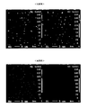
- FIG. 4 shows a cross section in the thickness direction of the internal electrode at the center of the laminate.
- the relatively dark color area is the internal electrode. From FIG. 4, it can be seen that, compared to the comparative example, the embodiment achieves a thinner layer while ensuring the continuity of the internal electrodes.
- FIG. 5 shows the surface state of the internal electrode at the center of the laminate.
- a relatively dark spot is a deficient portion of the internal electrode. From FIG. 5, it can be seen that, according to the example, higher coverage of the internal electrode is achieved as compared with the comparative example.
- FIG. 6 shows a cross section in the thickness direction at the end of the internal electrode.
- the relatively light colored area is the internal electrode. From FIG. 6, it can be seen that, according to the example, generation of voids and gaps at the end of the internal electrode is suppressed as compared with the comparative example.
- FIG. 7 shows a WDX mapping image of the ceramic layer at the center of the laminate.
- FIG. 7 particularly shows the segregation state of different phases (Mg and Si). These heterophases are indicated by relatively bright spots in FIG.
- Additive elements (Mg, Si, etc.) added to the ceramic constituting the ceramic layer are easily segregated after heat treatment, and the segregated heterogeneous phase often adversely affects the reliability of the ceramic layer.
- the segregation of the additive element is very small as compared with the comparative example. Therefore, according to the example, it can be seen that the characteristics are stable.
- FIG. 8 shows the lead-out portion of the internal electrode.
- the internal electrode was made thinner, but the amount of retraction at the lead-out portion was very small, and sintering was completed in a short time. For this reason, the movement and precipitation of the glass phase to the surface due to the additive component hardly occur. Therefore, when forming the external electrode, it is possible to omit the process for exposing the lead end portion of the internal electrode.
- Experimental Example 2 (Relationship between heating rate and electrode thickness) As shown in Table 2 below, the temperature increase rate was variously changed, and the minimum electrode thickness at which coverage of 80% or more was obtained in the internal electrode was determined.
- two types of samples were prepared, one using an Ni foil (Ni foil electrode) and one using a conductive paste containing Ni spherical powder (Ni spherical electrode) as an internal electrode. did.
- the conductive paste containing Ni spherical powder a paste having a relatively low filling rate of about 40 to 50% was used.
- Ni electrode A is a Ni foil electrode
- Ni electrode B is a Ni spherical electrode
- the thinning of the internal electrode is affected by the gap at the interface between the ceramic layer and the internal electrode. As shown in Table 2 and FIG. 9, at a heating rate of 15 ° C./second or less, the restraining force for the internal electrode having an electrode thickness of 0.3 ⁇ m or less cannot be maintained, and it is difficult to ensure coverage of 80% or more. On the other hand, since the ceramic is sintered and contracted in a short time by setting the temperature raising rate to 40 ° C./second or more, it is possible to ensure a coverage of 80% or more even at an electrode thickness of 0.3 ⁇ m or less. . Furthermore, by setting the rate of temperature rise to 100 ° C./second or more, 80% or more coverage can be secured even with an electrode thickness of 0.1 ⁇ m or less.
- the level of electrode thickness as described above varies depending on the filling rate of the conductive paste used.
- the electrode thickness must be relatively thick in order to ensure a predetermined coverage.
- Ni was used as the conductive component of the internal electrode, but the same applies to Cu, Ag, Pt, Pd, Al, Ti, Cr or alloys thereof other than Ni. There is a trend.
- the residual rate variation due to the size of the laminate can be reduced by increasing the rate of temperature rise, and in particular by setting the rate of temperature rise to 40 ° C./second or more, the residual rate variation is 1% or less. It can be seen that it can be suppressed.
- Experimental Example 4 (Relationship between maximum temperature holding time and electrode coverage) As described above, according to the present invention, it is possible to reduce the thickness of the internal electrode and increase the coverage, but these are also affected by the maximum temperature holding time in addition to the rate of temperature increase.
- FIG. 10 in order to obtain a multilayer body for a multilayer ceramic capacitor having an Ni internal electrode corresponding to an electrode thickness of 0.3 ⁇ m, after reaching 1380 ° C. at a temperature rising rate of 40 ° C./second, The relationship between retention time and electrode coverage is shown.
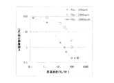
- Experimental Example 5 (Relationship between heating rate and Ni electrode oxidation degree)
- oxygen partial pressure (PO 2 ) in the heat treatment step three atmospheres of 100 ppm, 1000 ppm and 10000 ppm were adopted as shown in Table 4 and FIG. Table 4 and FIG. 11 show the relationship between the average temperature increase rate from room temperature to the maximum temperature under three oxygen partial pressures of 100 ppm, 1000 ppm, and 10000 ppm and the Ni electrode oxidation degree. These oxygen partial pressures were adjusted by introducing a predetermined amount of oxygen into the nitrogen atmosphere.
- Experimental Example 6 Influence of boundary surface between large grain region and small grain region
- samples 1 to 4 were prepared and evaluated for multilayer ceramic capacitors having a normal rectangular parallelepiped shape.
- the outline of Samples 1 to 4 is as follows.
- Sample 1 is an example within the scope of the present invention, and a boundary surface exists inside each of the LW surface and the LT surface.
- Samples 2 to 4 are comparative examples outside the scope of the present invention. In particular, sample 2 has a boundary surface only inside the LW surface, sample 3 has a boundary surface only inside the LT surface, and sample 4 has no boundary surface. is there.
- a ceramic green sheet B having a thickness of 5 ⁇ m was formed by the same method.
- a portion of the slurry prepared for forming the ceramic green sheet B was taken, and the solvent was partially removed to prepare a thickened ceramic slurry C.
- the ceramic slurry C was applied by a predetermined thickness on the surface to be the LT surface of the individual piece thus cut, and dried to set the side gap thickness to 145 ⁇ m on one side. Further cutting was performed to obtain a green laminated chip C.
- the green laminated chip A according to Sample 1 was fired under heating conditions of an average temperature rising rate of 40 ° C./second, a maximum temperature of 1300 ° C., and a maximum temperature holding time of 1 second.
- green laminated chips B, C, and D relating to each of Samples 2, 3, and 4 were fired under heating conditions of an average temperature rising rate of 0.17 ° C./second, a maximum temperature of 1220 ° C., and a maximum temperature holding time of 1 hour. did.
- the dimensions of the multilayer ceramic capacitor thus obtained were length L: 2.0 mm, width W: 1.2 mm, and thickness T: 1.2 mm.
- the thickness of the dielectric ceramic layer per layer was 2.0 ⁇ m.
- the area of the overlapping part of the internal electrodes was 2.0 mm 2 .
- the thickness of the outer layer portion was 120 ⁇ m, and the thickness of the side gap portion was 120 ⁇ m.
- FIG. 12 shows an SEM image obtained by imaging a cross section parallel to the LT surface of the multilayer ceramic capacitor multilayer body according to Sample 1.
- the upper end of FIG. 12 is at a distance of 60 ⁇ m from the outermost internal electrode, and the lower end of FIG. 12 is at a distance of 25 ⁇ m from the outermost internal electrode.
- FIG. 12 it is observed that the grain diameter distributions are different from each other inside and outside the boundary surface.
- the image analysis was performed on SEM photographs having an area per visual field of 12.5 ⁇ m 2 and 50 visual fields, and the grain diameter was determined. In each field of view, are arranged in ascending order of the grain diameter, total area of each grain, the grain diameter of the order reaching 80% of the entire field of view was defined as the 80 value D of the grain size distribution in its field of view.
- a region having a distance of 20 to 40 ⁇ m from the internal electrode corresponds to a region on the inner side of the boundary surface in the sample 1, for example.
- the maximum The values are shown in Table 6 as “maximum D 80 values in the 20-40 ⁇ m region”.
- the distance from the internal electrode is equivalent to 50 to 70 [mu] m in the region of the sample 1 at the boundary surface outer e.g. region of the D 80 value in this region, a minimum value, in Table 6, "50 ⁇ The value is shown as “Minimum D 80 value in 70 ⁇ m region”.
- Table 6 also shows the presence or absence of the boundary surface described above.
- the “maximum D 80 value in the 20 to 40 ⁇ m region” and the “minimum D 80 value in the 50 to 70 ⁇ m region” are naturally It shows the same value.
- the “minimum D 80 value in the 50 to 70 ⁇ m region” is larger than the “maximum D 80 value in the 20 to 40 ⁇ m region”.
- the latter “minimum D 80 value in the 50 to 70 ⁇ m region” was 5 times or more than the former “maximum D 80 value in the 20 to 40 ⁇ m region”.
- the capacitance (C DC0V ) of the multilayer ceramic capacitor according to each sample when no DC voltage is applied is measured at a temperature of 25 ° C. under the conditions of 120 Hz and 1.0 V using an automatic bridge type measuring instrument. did.
- the capacitance under application of a DC voltage was determined as the capacitance (C DC4V ) when a DC voltage of 4 V was applied for 1 second.
- the sample of the multilayer ceramic capacitor to be measured was heated at a temperature of 150 ° C. for 1 hour, and the voltage was applied at a temperature of 25 ° C. until the measurement was performed after the heating. The process which stored without applying is performed.
- the dielectric constant change rate ( ⁇ ) is small.
- the minimum "50 ⁇ 70 [mu] m region as compared with Sample 1 the boundary surface is present in both the outer portion and the side gap portion, and" maximum D 80 value of 20 ⁇ 40 [mu] m region " “D 80 value” indicates a large value. Therefore, as in Sample 1, the large grain region is located outside the small grain region, and the boundary surface between the large grain region and the grain region is outside the portion where the internal electrode exists, and the outer layer portion.
- the ceramic layer is located inside the outer surface of the laminate so as to extend along the side gap portion, it can be seen that the DC bias characteristics can be maintained well even when the ceramic layer is thinned.
- a temperature profile in which the average rate of temperature increase from room temperature to the maximum temperature is 40 ° C./second or more is used. It can be seen that it is effective to employ a heat treatment step.
Landscapes
- Engineering & Computer Science (AREA)
- Chemical & Material Sciences (AREA)
- Power Engineering (AREA)
- Manufacturing & Machinery (AREA)
- Ceramic Engineering (AREA)
- Microelectronics & Electronic Packaging (AREA)
- Inorganic Chemistry (AREA)
- Materials Engineering (AREA)
- Structural Engineering (AREA)
- Organic Chemistry (AREA)
- Ceramic Capacitors (AREA)
- Fixed Capacitors And Capacitor Manufacturing Machines (AREA)
Priority Applications (5)
| Application Number | Priority Date | Filing Date | Title |
|---|---|---|---|
| CN201080002124.3A CN102099880B (zh) | 2009-06-15 | 2010-05-21 | 层叠陶瓷电子部件及其制造方法 |
| KR1020117000219A KR101143128B1 (ko) | 2009-06-15 | 2010-05-21 | 적층 세라믹 전자부품 및 그 제조방법 |
| JP2010543339A JP5287869B2 (ja) | 2009-06-15 | 2010-05-21 | 積層セラミック電子部品およびその製造方法 |
| US13/004,213 US8540832B2 (en) | 2009-06-15 | 2011-01-11 | Laminated ceramic electronic component and manufacturing method therefor |
| US13/956,616 US9183986B2 (en) | 2009-06-15 | 2013-08-01 | Laminated ceramic electronic component and manufacturing method therefor |
Applications Claiming Priority (4)
| Application Number | Priority Date | Filing Date | Title |
|---|---|---|---|
| JP2009141866 | 2009-06-15 | ||
| JP2009-141866 | 2009-06-15 | ||
| JP2009156655 | 2009-07-01 | ||
| JP2009-156655 | 2009-07-01 |
Related Child Applications (1)
| Application Number | Title | Priority Date | Filing Date |
|---|---|---|---|
| US13/004,213 Continuation US8540832B2 (en) | 2009-06-15 | 2011-01-11 | Laminated ceramic electronic component and manufacturing method therefor |
Publications (1)
| Publication Number | Publication Date |
|---|---|
| WO2010146967A1 true WO2010146967A1 (ja) | 2010-12-23 |
Family
ID=43356288
Family Applications (1)
| Application Number | Title | Priority Date | Filing Date |
|---|---|---|---|
| PCT/JP2010/058618 WO2010146967A1 (ja) | 2009-06-15 | 2010-05-21 | 積層セラミック電子部品およびその製造方法 |
Country Status (6)
| Country | Link |
|---|---|
| US (2) | US8540832B2 (zh) |
| JP (1) | JP5287869B2 (zh) |
| KR (1) | KR101143128B1 (zh) |
| CN (1) | CN102099880B (zh) |
| TW (1) | TWI424455B (zh) |
| WO (1) | WO2010146967A1 (zh) |
Cited By (12)
| Publication number | Priority date | Publication date | Assignee | Title |
|---|---|---|---|---|
| WO2012111592A1 (ja) * | 2011-02-14 | 2012-08-23 | 株式会社村田製作所 | 積層セラミックコンデンサ及び積層セラミックコンデンサの製造方法 |
| JP2013055333A (ja) * | 2011-08-31 | 2013-03-21 | Samsung Electro-Mechanics Co Ltd | 磁性基板及びその製造方法 |
| JP2013157459A (ja) * | 2012-01-30 | 2013-08-15 | Tdk Corp | 積層セラミックコンデンサ |
| US20130222973A1 (en) * | 2010-11-24 | 2013-08-29 | Murata Manufacturing Co., Ltd. | Laminated Ceramic Electronic Component and Manufacturing Method Therefor |
| JP5298255B1 (ja) * | 2012-06-19 | 2013-09-25 | 太陽誘電株式会社 | 積層セラミックコンデンサ |
| JP2013229546A (ja) * | 2012-04-26 | 2013-11-07 | Samsung Electro-Mechanics Co Ltd | 積層セラミック電子部品及びその製造方法 |
| JP2014082462A (ja) * | 2012-09-27 | 2014-05-08 | Taiyo Yuden Co Ltd | 積層セラミックコンデンサ |
| JP2014093515A (ja) * | 2012-11-06 | 2014-05-19 | Samsung Electro-Mechanics Co Ltd | 積層セラミック電子部品 |
| JPWO2013175945A1 (ja) * | 2012-05-24 | 2016-01-12 | 株式会社村田製作所 | 積層セラミック電子部品 |
| JP2018098489A (ja) * | 2016-12-14 | 2018-06-21 | サムソン エレクトロ−メカニックス カンパニーリミテッド. | インダクタ |
| JP2018142728A (ja) * | 2016-02-18 | 2018-09-13 | 太陽誘電株式会社 | 積層セラミックコンデンサ |
| JP2019029422A (ja) * | 2017-07-26 | 2019-02-21 | 太陽誘電株式会社 | 積層セラミックコンデンサおよびその製造方法 |
Families Citing this family (21)
| Publication number | Priority date | Publication date | Assignee | Title |
|---|---|---|---|---|
| CN102473523B (zh) * | 2009-08-20 | 2014-07-23 | 株式会社村田制作所 | 层叠陶瓷电容器的制造方法以及层叠陶瓷电容器 |
| US20140252693A1 (en) * | 2011-08-05 | 2014-09-11 | Murata Manufacturing Co., Ltd. | Method for manufacturing ceramic electronic component |
| JP5556854B2 (ja) * | 2012-06-12 | 2014-07-23 | 株式会社村田製作所 | セラミック電子部品の製造方法及びセラミック電子部品 |
| KR101983130B1 (ko) | 2012-09-06 | 2019-05-28 | 삼성전기주식회사 | 적층형 세라믹 커패시터 및 그 제조방법 |
| JP2015126219A (ja) * | 2013-12-27 | 2015-07-06 | 株式会社村田製作所 | 積層セラミックコンデンサ |
| JP2015126220A (ja) * | 2013-12-27 | 2015-07-06 | 株式会社村田製作所 | 積層セラミックコンデンサ |
| JP6439551B2 (ja) * | 2014-05-21 | 2018-12-19 | 株式会社村田製作所 | 積層セラミックコンデンサ |
| JP6665438B2 (ja) | 2015-07-17 | 2020-03-13 | 株式会社村田製作所 | 積層セラミックコンデンサ |
| JP6793027B2 (ja) * | 2016-12-16 | 2020-12-02 | 太陽誘電株式会社 | 積層セラミック電子部品 |
| JP6888324B2 (ja) * | 2017-02-23 | 2021-06-16 | 株式会社村田製作所 | 積層セラミック電子部品の製造方法 |
| JP2020167283A (ja) * | 2019-03-29 | 2020-10-08 | 株式会社村田製作所 | 積層セラミックコンデンサ |
| KR102257992B1 (ko) * | 2019-07-08 | 2021-05-28 | 삼성전기주식회사 | 커패시터 부품 |
| KR102333094B1 (ko) * | 2019-07-08 | 2021-12-01 | 삼성전기주식회사 | 커패시터 부품 |
| JP2021034648A (ja) * | 2019-08-28 | 2021-03-01 | 株式会社村田製作所 | 積層セラミックコンデンサ |
| WO2021166191A1 (ja) * | 2020-02-20 | 2021-08-26 | 日本碍子株式会社 | セラミックス成形体の誘電乾燥方法及び誘電乾燥装置、並びにセラミックス構造体の製造方法 |
| JP2022095349A (ja) * | 2020-12-16 | 2022-06-28 | 太陽誘電株式会社 | 積層セラミックコンデンサおよび積層セラミックコンデンサの製造方法 |
| US11961681B2 (en) * | 2020-12-28 | 2024-04-16 | Samsung Electro-Mechanics Co., Ltd. | Multilayer capacitor including internal electrodes having pores on ends thereof and board having the same mounted thereon |
| JP2022143334A (ja) * | 2021-03-17 | 2022-10-03 | 太陽誘電株式会社 | セラミック電子部品およびその製造方法 |
| US20220392706A1 (en) * | 2021-05-25 | 2022-12-08 | Samsung Electro-Mechanics Co., Ltd. | Multilayered electronic component |
| US20220392703A1 (en) * | 2021-05-25 | 2022-12-08 | Samsung Electro-Mechanics Co., Ltd. | Mutilayer electronic component and method of manufacturing the same |
| KR20230100937A (ko) * | 2021-12-29 | 2023-07-06 | 삼성전기주식회사 | 적층형 전자 부품 |
Citations (6)
| Publication number | Priority date | Publication date | Assignee | Title |
|---|---|---|---|---|
| JPH06267785A (ja) * | 1993-03-12 | 1994-09-22 | Toshiba Corp | 積層セラミック電子部品の製造方法 |
| JPH10149941A (ja) * | 1996-11-18 | 1998-06-02 | Toyota Central Res & Dev Lab Inc | 多層基板の製造方法 |
| JPH10241987A (ja) * | 1997-02-25 | 1998-09-11 | Tokin Corp | 積層セラミックコンデンサの製造方法 |
| JP2002289457A (ja) * | 2001-03-28 | 2002-10-04 | Kyocera Corp | 積層セラミック電子部品の製造方法 |
| KR20060135249A (ko) * | 2005-06-24 | 2006-12-29 | 삼성전기주식회사 | 적층형 칩의 고속 승온 소성 방법 |
| JP2008226941A (ja) * | 2007-03-09 | 2008-09-25 | Matsushita Electric Ind Co Ltd | セラミックコンデンサの製造方法 |
Family Cites Families (15)
| Publication number | Priority date | Publication date | Assignee | Title |
|---|---|---|---|---|
| US4039338A (en) * | 1972-12-29 | 1977-08-02 | International Business Machines Corporation | Accelerated sintering for a green ceramic sheet |
| US4490319A (en) * | 1983-10-26 | 1984-12-25 | General Electric Company | Rapid rate sintering of ceramics |
| US5260094A (en) * | 1991-09-30 | 1993-11-09 | Cornell Research Foundation, Inc. | Preparing densified low porosity titania sol-gel forms |
| US5391339A (en) * | 1992-12-31 | 1995-02-21 | Valenite Inc. | Continuous process for producing alumina-titanium carbide composites |
| JPH08264721A (ja) * | 1995-03-28 | 1996-10-11 | Olympus Optical Co Ltd | 誘電体キャパシタ |
| JPH11163273A (ja) * | 1997-12-01 | 1999-06-18 | Tokyo Ohka Kogyo Co Ltd | 誘電体薄膜、誘電体キャパシタの製造方法、および誘電体メモリ |
| JP4803854B2 (ja) | 1999-01-27 | 2011-10-26 | Tdk株式会社 | 積層型セラミックコンデンサの製造方法 |
| JP4551991B2 (ja) | 2000-06-27 | 2010-09-29 | ルネサスエレクトロニクス株式会社 | プラズマエッチング方法およびこれを用いて製造された半導体装置 |
| JP2001284341A (ja) | 2001-02-22 | 2001-10-12 | Tokyo Electron Ltd | 熱処理方法 |
| JP4407299B2 (ja) * | 2004-01-30 | 2010-02-03 | Tdk株式会社 | 積層セラミックコンデンサ |
| JP4574267B2 (ja) * | 2004-07-28 | 2010-11-04 | 京セラ株式会社 | 積層型電子部品の製法および積層型電子部品 |
| JP2006165259A (ja) | 2004-12-07 | 2006-06-22 | Kyocera Corp | 誘電体磁器および積層型電子部品 |
| JP2007173480A (ja) * | 2005-12-21 | 2007-07-05 | Tdk Corp | 積層型電子部品およびその製造方法 |
| JP5164463B2 (ja) * | 2007-07-26 | 2013-03-21 | 太陽誘電株式会社 | 積層セラミックコンデンサの製造方法及び積層セラミックコンデンサ |
| CN102473523B (zh) * | 2009-08-20 | 2014-07-23 | 株式会社村田制作所 | 层叠陶瓷电容器的制造方法以及层叠陶瓷电容器 |
-
2010
- 2010-05-21 KR KR1020117000219A patent/KR101143128B1/ko active IP Right Grant
- 2010-05-21 JP JP2010543339A patent/JP5287869B2/ja active Active
- 2010-05-21 CN CN201080002124.3A patent/CN102099880B/zh active Active
- 2010-05-21 WO PCT/JP2010/058618 patent/WO2010146967A1/ja active Application Filing
- 2010-05-31 TW TW099117472A patent/TWI424455B/zh active
-
2011
- 2011-01-11 US US13/004,213 patent/US8540832B2/en active Active
-
2013
- 2013-08-01 US US13/956,616 patent/US9183986B2/en active Active
Patent Citations (6)
| Publication number | Priority date | Publication date | Assignee | Title |
|---|---|---|---|---|
| JPH06267785A (ja) * | 1993-03-12 | 1994-09-22 | Toshiba Corp | 積層セラミック電子部品の製造方法 |
| JPH10149941A (ja) * | 1996-11-18 | 1998-06-02 | Toyota Central Res & Dev Lab Inc | 多層基板の製造方法 |
| JPH10241987A (ja) * | 1997-02-25 | 1998-09-11 | Tokin Corp | 積層セラミックコンデンサの製造方法 |
| JP2002289457A (ja) * | 2001-03-28 | 2002-10-04 | Kyocera Corp | 積層セラミック電子部品の製造方法 |
| KR20060135249A (ko) * | 2005-06-24 | 2006-12-29 | 삼성전기주식회사 | 적층형 칩의 고속 승온 소성 방법 |
| JP2008226941A (ja) * | 2007-03-09 | 2008-09-25 | Matsushita Electric Ind Co Ltd | セラミックコンデンサの製造方法 |
Cited By (24)
| Publication number | Priority date | Publication date | Assignee | Title |
|---|---|---|---|---|
| US20130222973A1 (en) * | 2010-11-24 | 2013-08-29 | Murata Manufacturing Co., Ltd. | Laminated Ceramic Electronic Component and Manufacturing Method Therefor |
| US9136058B2 (en) * | 2010-11-24 | 2015-09-15 | Murata Manufacturing Co., Ltd. | Laminated ceramic electronic component and manufacturing method therefor |
| US9099244B2 (en) | 2011-02-14 | 2015-08-04 | Murata Manufacturing Co., Ltd. | Multilayer ceramic capacitor and method for manufacturing multilayer ceramic capacitor |
| WO2012111592A1 (ja) * | 2011-02-14 | 2012-08-23 | 株式会社村田製作所 | 積層セラミックコンデンサ及び積層セラミックコンデンサの製造方法 |
| JP5488725B2 (ja) * | 2011-02-14 | 2014-05-14 | 株式会社村田製作所 | 積層セラミックコンデンサの製造方法 |
| JP2013055333A (ja) * | 2011-08-31 | 2013-03-21 | Samsung Electro-Mechanics Co Ltd | 磁性基板及びその製造方法 |
| JP2013157459A (ja) * | 2012-01-30 | 2013-08-15 | Tdk Corp | 積層セラミックコンデンサ |
| KR101823160B1 (ko) * | 2012-04-26 | 2018-01-29 | 삼성전기주식회사 | 적층 세라믹 전자부품 및 이의 제조방법 |
| JP2013229546A (ja) * | 2012-04-26 | 2013-11-07 | Samsung Electro-Mechanics Co Ltd | 積層セラミック電子部品及びその製造方法 |
| JPWO2013175945A1 (ja) * | 2012-05-24 | 2016-01-12 | 株式会社村田製作所 | 積層セラミック電子部品 |
| WO2013190718A1 (ja) * | 2012-06-19 | 2013-12-27 | 太陽誘電株式会社 | 積層セラミックコンデンサ |
| US9607766B2 (en) | 2012-06-19 | 2017-03-28 | Taiyo Yuden Co., Ltd. | Laminated ceramic capacitor |
| JP5298255B1 (ja) * | 2012-06-19 | 2013-09-25 | 太陽誘電株式会社 | 積層セラミックコンデンサ |
| JP2014082462A (ja) * | 2012-09-27 | 2014-05-08 | Taiyo Yuden Co Ltd | 積層セラミックコンデンサ |
| JP2014093515A (ja) * | 2012-11-06 | 2014-05-19 | Samsung Electro-Mechanics Co Ltd | 積層セラミック電子部品 |
| JP2022020816A (ja) * | 2016-02-18 | 2022-02-01 | 太陽誘電株式会社 | 積層セラミックコンデンサ |
| JP2018142728A (ja) * | 2016-02-18 | 2018-09-13 | 太陽誘電株式会社 | 積層セラミックコンデンサ |
| JP2021010036A (ja) * | 2016-02-18 | 2021-01-28 | 太陽誘電株式会社 | 積層セラミックコンデンサ及びその製造方法 |
| JP7019781B2 (ja) | 2016-02-18 | 2022-02-15 | 太陽誘電株式会社 | 積層セラミックコンデンサ及びその製造方法 |
| JP7326407B2 (ja) | 2016-02-18 | 2023-08-15 | 太陽誘電株式会社 | 積層セラミックコンデンサ |
| US10490332B2 (en) | 2016-12-14 | 2019-11-26 | Samsung Electro-Mechanics Co., Ltd. | Inductor |
| JP2018098489A (ja) * | 2016-12-14 | 2018-06-21 | サムソン エレクトロ−メカニックス カンパニーリミテッド. | インダクタ |
| JP2019029422A (ja) * | 2017-07-26 | 2019-02-21 | 太陽誘電株式会社 | 積層セラミックコンデンサおよびその製造方法 |
| JP7227690B2 (ja) | 2017-07-26 | 2023-02-22 | 太陽誘電株式会社 | 積層セラミックコンデンサおよびその製造方法 |
Also Published As
| Publication number | Publication date |
|---|---|
| US20140078641A1 (en) | 2014-03-20 |
| TW201108275A (en) | 2011-03-01 |
| JPWO2010146967A1 (ja) | 2012-12-06 |
| CN102099880B (zh) | 2015-03-25 |
| KR101143128B1 (ko) | 2012-05-08 |
| US8540832B2 (en) | 2013-09-24 |
| KR20110018936A (ko) | 2011-02-24 |
| CN102099880A (zh) | 2011-06-15 |
| US9183986B2 (en) | 2015-11-10 |
| US20110110014A1 (en) | 2011-05-12 |
| JP5287869B2 (ja) | 2013-09-11 |
| TWI424455B (zh) | 2014-01-21 |
Similar Documents
| Publication | Publication Date | Title |
|---|---|---|
| JP5287869B2 (ja) | 積層セラミック電子部品およびその製造方法 | |
| CN108257779B (zh) | 层叠陶瓷电子部件 | |
| JP5316642B2 (ja) | 積層セラミックコンデンサの製造方法および積層セラミックコンデンサ | |
| JP4858248B2 (ja) | 誘電体磁器組成物および電子部品 | |
| JP7091584B2 (ja) | 誘電体組成物及び積層型電子部品 | |
| JP4483597B2 (ja) | 電子部品、誘電体磁器組成物およびその製造方法 | |
| JP5316641B2 (ja) | 積層セラミックコンデンサの製造方法および積層セラミックコンデンサ | |
| KR20070088360A (ko) | 유전체 자기조성물 및 그 제조방법 | |
| JP2009044017A (ja) | 積層セラミックコンデンサおよび積層セラミックコンデンサの製造方法 | |
| KR100720804B1 (ko) | 세라믹 전자 부품 및 그 제조방법 | |
| JP2007173480A (ja) | 積層型電子部品およびその製造方法 | |
| JP2005294317A (ja) | 積層セラミックコンデンサ | |
| CN112992538B (zh) | 电介质组合物及电子部件 | |
| JP4710908B2 (ja) | 誘電体磁器組成物および電子部品 | |
| JP4561922B2 (ja) | 誘電体磁器組成物、電子部品およびこれらの製造方法 | |
| JP2010024126A (ja) | 誘電体磁器組成物 | |
| JP2008247657A (ja) | 誘電体磁器組成物および電子部品 | |
| JP4661203B2 (ja) | セラミック電子部品およびその製造方法 | |
| KR100581398B1 (ko) | 유전체 자기조성물, 전자부품 및 이들의 제조방법 | |
| JP2007258477A (ja) | 積層型電子部品およびその製造方法 | |
| JP2008222521A (ja) | 誘電体磁器組成物および電子部品 | |
| JP2019067827A (ja) | 積層電子部品 | |
| JP5114861B2 (ja) | 誘電体磁器組成物および電子部品 | |
| JP2007157769A (ja) | 積層型電子部品 | |
| KR101115647B1 (ko) | 유전체 자기 조성물, 전자 부품 및 이들의 제조 방법 |
Legal Events
| Date | Code | Title | Description |
|---|---|---|---|
| WWE | Wipo information: entry into national phase |
Ref document number: 201080002124.3 Country of ref document: CN |
|
| ENP | Entry into the national phase |
Ref document number: 2010543339 Country of ref document: JP Kind code of ref document: A |
|
| ENP | Entry into the national phase |
Ref document number: 20117000219 Country of ref document: KR Kind code of ref document: A |
|
| 121 | Ep: the epo has been informed by wipo that ep was designated in this application |
Ref document number: 10789342 Country of ref document: EP Kind code of ref document: A1 |
|
| NENP | Non-entry into the national phase |
Ref country code: DE |
|
| 122 | Ep: pct application non-entry in european phase |
Ref document number: 10789342 Country of ref document: EP Kind code of ref document: A1 |