WO2009142235A1 - Dispositif ci sans fil et son procédé de fabrication - Google Patents
Dispositif ci sans fil et son procédé de fabrication Download PDFInfo
- Publication number
- WO2009142235A1 WO2009142235A1 PCT/JP2009/059259 JP2009059259W WO2009142235A1 WO 2009142235 A1 WO2009142235 A1 WO 2009142235A1 JP 2009059259 W JP2009059259 W JP 2009059259W WO 2009142235 A1 WO2009142235 A1 WO 2009142235A1
- Authority
- WO
- WIPO (PCT)
- Prior art keywords
- wireless
- coil
- normal direction
- insulating sheet
- connection portion
- Prior art date
Links
- 238000000034 method Methods 0.000 title claims abstract description 33
- 238000004519 manufacturing process Methods 0.000 title claims abstract description 27
- 239000004020 conductor Substances 0.000 claims description 56
- 230000008878 coupling Effects 0.000 claims description 8
- 238000010168 coupling process Methods 0.000 claims description 8
- 238000005859 coupling reaction Methods 0.000 claims description 8
- 230000005540 biological transmission Effects 0.000 claims description 6
- 238000010030 laminating Methods 0.000 claims description 6
- 239000003990 capacitor Substances 0.000 description 22
- 238000010586 diagram Methods 0.000 description 17
- 239000000919 ceramic Substances 0.000 description 12
- 239000000758 substrate Substances 0.000 description 8
- 230000015572 biosynthetic process Effects 0.000 description 6
- 239000004148 curcumin Substances 0.000 description 6
- 239000011888 foil Substances 0.000 description 5
- 239000000463 material Substances 0.000 description 5
- 101100229939 Mus musculus Gpsm1 gene Proteins 0.000 description 4
- 238000013459 approach Methods 0.000 description 4
- 230000007423 decrease Effects 0.000 description 4
- 229910052751 metal Inorganic materials 0.000 description 4
- 239000002184 metal Substances 0.000 description 4
- 229920000139 polyethylene terephthalate Polymers 0.000 description 4
- 239000005020 polyethylene terephthalate Substances 0.000 description 4
- 229920005989 resin Polymers 0.000 description 4
- 239000011347 resin Substances 0.000 description 4
- 239000000853 adhesive Substances 0.000 description 3
- 230000001070 adhesive effect Effects 0.000 description 3
- 238000013461 design Methods 0.000 description 3
- 230000001678 irradiating effect Effects 0.000 description 3
- RYGMFSIKBFXOCR-UHFFFAOYSA-N Copper Chemical compound [Cu] RYGMFSIKBFXOCR-UHFFFAOYSA-N 0.000 description 2
- 229920000106 Liquid crystal polymer Polymers 0.000 description 2
- 239000004977 Liquid-crystal polymers (LCPs) Substances 0.000 description 2
- 239000004642 Polyimide Substances 0.000 description 2
- BZHJMEDXRYGGRV-UHFFFAOYSA-N Vinyl chloride Chemical compound ClC=C BZHJMEDXRYGGRV-UHFFFAOYSA-N 0.000 description 2
- 239000011889 copper foil Substances 0.000 description 2
- 238000005520 cutting process Methods 0.000 description 2
- 239000003989 dielectric material Substances 0.000 description 2
- 230000000694 effects Effects 0.000 description 2
- 238000005530 etching Methods 0.000 description 2
- 238000002474 experimental method Methods 0.000 description 2
- 238000003475 lamination Methods 0.000 description 2
- -1 polyethylene terephthalate Polymers 0.000 description 2
- 229920001721 polyimide Polymers 0.000 description 2
- 238000003825 pressing Methods 0.000 description 2
- 238000007650 screen-printing Methods 0.000 description 2
- 101710187785 60S ribosomal protein L1-A Proteins 0.000 description 1
- 101710187786 60S ribosomal protein L1-B Proteins 0.000 description 1
- 239000004593 Epoxy Substances 0.000 description 1
- 229910052782 aluminium Inorganic materials 0.000 description 1
- XAGFODPZIPBFFR-UHFFFAOYSA-N aluminium Chemical compound [Al] XAGFODPZIPBFFR-UHFFFAOYSA-N 0.000 description 1
- 229910010293 ceramic material Inorganic materials 0.000 description 1
- 238000005094 computer simulation Methods 0.000 description 1
- 230000003247 decreasing effect Effects 0.000 description 1
- 230000002950 deficient Effects 0.000 description 1
- 230000005674 electromagnetic induction Effects 0.000 description 1
- 238000010304 firing Methods 0.000 description 1
- 230000004907 flux Effects 0.000 description 1
- 239000011521 glass Substances 0.000 description 1
- 230000010365 information processing Effects 0.000 description 1
- 238000003780 insertion Methods 0.000 description 1
- 230000037431 insertion Effects 0.000 description 1
- 239000011810 insulating material Substances 0.000 description 1
- 230000003071 parasitic effect Effects 0.000 description 1
- 230000000149 penetrating effect Effects 0.000 description 1
- 229920005644 polyethylene terephthalate glycol copolymer Polymers 0.000 description 1
- 238000002360 preparation method Methods 0.000 description 1
- 238000007639 printing Methods 0.000 description 1
- 238000012545 processing Methods 0.000 description 1
- 239000004065 semiconductor Substances 0.000 description 1
Images


Classifications
-
- H—ELECTRICITY
- H01—ELECTRIC ELEMENTS
- H01Q—ANTENNAS, i.e. RADIO AERIALS
- H01Q1/00—Details of, or arrangements associated with, antennas
- H01Q1/12—Supports; Mounting means
- H01Q1/22—Supports; Mounting means by structural association with other equipment or articles
- H01Q1/2208—Supports; Mounting means by structural association with other equipment or articles associated with components used in interrogation type services, i.e. in systems for information exchange between an interrogator/reader and a tag/transponder, e.g. in Radio Frequency Identification [RFID] systems
- H01Q1/2225—Supports; Mounting means by structural association with other equipment or articles associated with components used in interrogation type services, i.e. in systems for information exchange between an interrogator/reader and a tag/transponder, e.g. in Radio Frequency Identification [RFID] systems used in active tags, i.e. provided with its own power source or in passive tags, i.e. deriving power from RF signal
-
- G—PHYSICS
- G06—COMPUTING; CALCULATING OR COUNTING
- G06K—GRAPHICAL DATA READING; PRESENTATION OF DATA; RECORD CARRIERS; HANDLING RECORD CARRIERS
- G06K19/00—Record carriers for use with machines and with at least a part designed to carry digital markings
- G06K19/06—Record carriers for use with machines and with at least a part designed to carry digital markings characterised by the kind of the digital marking, e.g. shape, nature, code
- G06K19/067—Record carriers with conductive marks, printed circuits or semiconductor circuit elements, e.g. credit or identity cards also with resonating or responding marks without active components
- G06K19/07—Record carriers with conductive marks, printed circuits or semiconductor circuit elements, e.g. credit or identity cards also with resonating or responding marks without active components with integrated circuit chips
- G06K19/077—Constructional details, e.g. mounting of circuits in the carrier
- G06K19/07749—Constructional details, e.g. mounting of circuits in the carrier the record carrier being capable of non-contact communication, e.g. constructional details of the antenna of a non-contact smart card
- G06K19/07773—Antenna details
- G06K19/07777—Antenna details the antenna being of the inductive type
- G06K19/07779—Antenna details the antenna being of the inductive type the inductive antenna being a coil
- G06K19/07783—Antenna details the antenna being of the inductive type the inductive antenna being a coil the coil being planar
-
- G—PHYSICS
- G06—COMPUTING; CALCULATING OR COUNTING
- G06K—GRAPHICAL DATA READING; PRESENTATION OF DATA; RECORD CARRIERS; HANDLING RECORD CARRIERS
- G06K19/00—Record carriers for use with machines and with at least a part designed to carry digital markings
- G06K19/06—Record carriers for use with machines and with at least a part designed to carry digital markings characterised by the kind of the digital marking, e.g. shape, nature, code
- G06K19/067—Record carriers with conductive marks, printed circuits or semiconductor circuit elements, e.g. credit or identity cards also with resonating or responding marks without active components
- G06K19/07—Record carriers with conductive marks, printed circuits or semiconductor circuit elements, e.g. credit or identity cards also with resonating or responding marks without active components with integrated circuit chips
- G06K19/077—Constructional details, e.g. mounting of circuits in the carrier
- G06K19/07749—Constructional details, e.g. mounting of circuits in the carrier the record carrier being capable of non-contact communication, e.g. constructional details of the antenna of a non-contact smart card
- G06K19/07773—Antenna details
- G06K19/07777—Antenna details the antenna being of the inductive type
- G06K19/07784—Antenna details the antenna being of the inductive type the inductive antenna consisting of a plurality of coils stacked on top of one another
-
- H—ELECTRICITY
- H01—ELECTRIC ELEMENTS
- H01Q—ANTENNAS, i.e. RADIO AERIALS
- H01Q1/00—Details of, or arrangements associated with, antennas
- H01Q1/36—Structural form of radiating elements, e.g. cone, spiral, umbrella; Particular materials used therewith
- H01Q1/38—Structural form of radiating elements, e.g. cone, spiral, umbrella; Particular materials used therewith formed by a conductive layer on an insulating support
-
- H—ELECTRICITY
- H01—ELECTRIC ELEMENTS
- H01Q—ANTENNAS, i.e. RADIO AERIALS
- H01Q7/00—Loop antennas with a substantially uniform current distribution around the loop and having a directional radiation pattern in a plane perpendicular to the plane of the loop
-
- H04B5/26—
-
- Y—GENERAL TAGGING OF NEW TECHNOLOGICAL DEVELOPMENTS; GENERAL TAGGING OF CROSS-SECTIONAL TECHNOLOGIES SPANNING OVER SEVERAL SECTIONS OF THE IPC; TECHNICAL SUBJECTS COVERED BY FORMER USPC CROSS-REFERENCE ART COLLECTIONS [XRACs] AND DIGESTS
- Y10—TECHNICAL SUBJECTS COVERED BY FORMER USPC
- Y10T—TECHNICAL SUBJECTS COVERED BY FORMER US CLASSIFICATION
- Y10T29/00—Metal working
- Y10T29/49—Method of mechanical manufacture
- Y10T29/49002—Electrical device making
- Y10T29/49117—Conductor or circuit manufacturing
- Y10T29/49124—On flat or curved insulated base, e.g., printed circuit, etc.
Definitions
- the present invention relates to a wireless IC (Integrated Circuit) device and a manufacturing method thereof, and more specifically, to a wireless IC device having a wireless IC used for an RFID (Radio Frequency Identification) system and a manufacturing method thereof.
- a wireless IC Integrated Circuit
- RFID Radio Frequency Identification
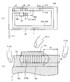
- a non-contact IC card described in Patent Document 1 is known as a wireless IC device used for entrance / exit management, commuter pass, credit card, and the like.
- 19A is a top view of the non-contact IC card 100 described in Patent Document 1
- FIG. 19B is a bottom view of the non-contact IC card 100 described in Patent Document 1.
- an antenna coil 104 that spirals around a plurality of times is formed on the main surface of the substrate 102, and an adjustment resistor (not shown in FIG. 19) is formed on the antenna coil 104.
- an adjustment capacitor 108 is connected.
- An IC 106 is connected to the antenna coil 104. According to the non-contact IC card, the resistance value and the capacitance value of the non-contact IC card 100 are adjusted by cutting a part of the adjustment resistor and the adjustment capacitor 108 at the time of manufacture, so that the resonance frequency and the sharpness (Q ) Can be adjusted.
- FIG. 20A is a cross-sectional structural view taken along the line BB of the antenna coil and the substrate of the non-contact IC card 100
- FIG. 20B is an equivalent circuit diagram of the non-contact IC card 100.
- FIG. FIG. 20A shows the substrate 102 and the antenna coil 104.
- FIG. 20B shows the inductance L100 of the antenna coil 104, the resistance R100 of the IC 106, and the capacitance C100 of the antenna coil 104.
- the antenna coil 104 is spirally wound around the main surface of the substrate 102 a plurality of times.
- the wirings constituting the antenna coil 104 are arranged close to each other on the main surface.
- an electric force line E100 connecting the wirings is generated as shown by an arrow due to a potential difference between the wirings, and a capacitance C100 is generated between the wirings.
- Such a capacitor C100 is connected in parallel between an inductance L100 and a resistor R100, as shown in FIG.
- the shape of the antenna coil 104 is designed so that an inductance L100 and a capacitance C100 having a desired resonance frequency can be obtained.
- the inventor of the present application has found that even if the shape of the antenna coil 104 is designed so that a desired resonance frequency can be obtained, the resonance frequency of the non-contact IC card 100 varies depending on the use situation. Therefore, the inventor of the present application conducted experiments and computer simulations to investigate the reason why the resonance frequency of the non-contact IC card 100 varies. As a result, it has been found that the phenomenon described below occurs in the non-contact IC card 100 as a cause of variation in the resonance frequency.
- the non-contact IC card 100 is used as, for example, entrance / exit management, commuter pass, credit card and the like.
- a non-contact IC card 100 is normally used close to a dedicated reader / writer while being held by a human hand.
- a human hand is positioned near the antenna coil 104, and the electric lines of force E100 pass through the human hand. Since the dielectric constant of a human hand is much larger than the dielectric constant of air, when a human hand approaches between the wirings of the antenna coil 104, the capacitance C100 generated between the wirings of the antenna coil 104 increases. As a result, the resonance frequency of the non-contact IC card 100 becomes lower than a desired resonance frequency.
- the positional relationship between the wiring of the antenna coil 104 and the human hand is not constant.
- the increase amount of the capacity C100 also varies depending on the use situation
- the decrease amount of the resonance frequency of the non-contact IC card 100 also varies depending on the use situation. That is, the resonance frequency of the non-contact IC card 100 varies depending on the use situation.
- the resonance frequency of the non-contact IC card 100 varies depending on the use situation.
- an object of the present invention is to provide a wireless IC device and a method for manufacturing the same, which can reduce the variation of the resonance frequency depending on the use situation.
- a wireless IC device includes an insulating sheet, and a plurality of coil electrodes that are provided with the insulating sheet interposed therebetween and that are connected to each other to form an antenna coil.
- the coil electrode is characterized in that when viewed in plan from the normal direction of the insulating sheet, it overlaps to form one ring.
- the method of manufacturing the wireless IC device includes a step of forming coil electrodes on a plurality of insulating sheets, and the plurality of coil electrodes overlapping when viewed in plan from the normal direction of the insulating sheets. And laminating the plurality of insulating sheets so as to form one ring.
- the plurality of coil electrodes constitute one ring by overlapping when viewed in plan from the normal direction of the insulating sheet. Therefore, in the wireless IC device, the coil electrodes are not lined up in the direction in which the main surface of the insulating sheet extends. As a result, the lines of electric force generated between the coil electrodes are prevented from leaking outside the wireless IC device. As a result, the capacitance generated in the coil electrode is changed depending on how the wireless IC device is held, and the resonance frequency of the wireless IC device is prevented from varying.
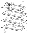
- FIG. 1 is an exploded perspective view of a wireless IC device according to a first embodiment.
- FIG. 2A is a plan view of the wireless IC device of FIG. 1 from the z-axis direction.
- FIG. 2B is a cross-sectional structure view taken along line AA of the wireless IC device shown in FIG.
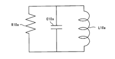
- FIG. 2 is an equivalent circuit diagram of the wireless IC device shown in FIG. 1.
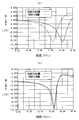
- FIG. 4A is a graph showing the loss characteristics of the first sample
- FIG. 4B is a graph showing the loss characteristics of the second sample. It is a disassembled perspective view of the radio
- FIG. 6 is a cross-sectional structure diagram of the wireless IC device of FIG. 5 in the zy plane.
- FIG. 8 is a cross-sectional structure diagram of the wireless IC device of FIG. 7 in the zy plane. It is a disassembled perspective view of the radio
- FIG. 10 is a cross-sectional structure diagram in the zy plane in the vicinity of the connection portion of the wireless IC device of FIG. 9.
- FIG. 11A is a top view of the wireless IC device according to the fifth embodiment.
- FIG. 11B is a bottom view of the wireless IC device according to the fifth embodiment. It is a disassembled perspective view of the radio
- FIG. 11A is a top view of the wireless IC device according to the fifth embodiment.
- FIG. 11B is a bottom view of the wireless IC device according to the fifth embodiment. It is a disassembled perspective view of the radio
- FIG. 13 is a cross-sectional structure diagram in the xz plane in the vicinity of the electromagnetic coupling module of the wireless IC device of FIG. 12. It is a disassembled perspective view of a feeder circuit board. It is a disassembled perspective view of the radio
- 16A is a cross-sectional structure diagram in the zy plane in the vicinity of the wireless IC of the wireless IC device according to the reference example
- FIG. 16B is a cross-sectional structure diagram in the zy plane in the vicinity of the wireless IC of the wireless IC device. is there. It is an enlarged view of the coil electrode of the radio
- FIG. 19A is a top view of the non-contact IC card described in Patent Document 1
- FIG. 19B is a bottom view of the non-contact IC card described in Patent Document 1.
- FIG. 20A is a cross-sectional structure diagram of the antenna coil and substrate BB of the non-contact IC card
- FIG. 20B is an equivalent circuit diagram of the non-contact IC card.
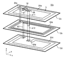
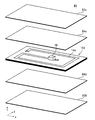
- FIG. 1 is an exploded perspective view of a wireless IC device 10a according to the first embodiment.
- the x axis is the long side direction of the wireless IC device 10a
- the y axis is the short side direction of the wireless IC device 10a
- the z axis is the stacking direction of the wireless IC device 10a.
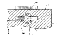
- FIG. 2A is a plan view of the wireless IC device 10a from the z-axis direction.
- FIG. 2B is a sectional structural view taken along line AA of the wireless IC device 10a shown in FIG. In FIG. 2, a human hand is shown, but it is shown much smaller than actual.
- FIG. 3 is an equivalent circuit diagram of the wireless IC device 10a shown in FIG.
- the wireless IC device 10a has a resonance frequency of 13.56 MHz and transmits a transmission / reception signal to / from the reader / writer by an electromagnetic induction method.
- the wireless IC device 10a includes insulating sheets 12a to 12d, coil electrodes 14a to 14d, a connection portion 16, a wireless IC 18, connection portions 20a and 20d, and via-hole conductors b1 to b3 and b11 to b13. I have.
- an alphabet or numeral is appended to the reference symbol, and when an element is generically referred to, the alphabet or number after the reference symbol is omitted.
- the insulating sheet 12 is a rectangular sheet made of an insulating material, and is made of, for example, vinyl chloride or a polyethylene terephthalate (PET) resin sheet.
- the normal direction of the insulating sheet 12 coincides with the z-axis direction.
- the coil electrodes 14a to 14d are formed on the insulating sheets 12a to 12d so as to have the same line width by a metal foil such as copper foil or aluminum foil, and are connected to each other to advance in the z-axis direction while rotating.
- a spiral antenna coil L is formed. More specifically, the coil electrode 14 has a shape in which four linear electrodes extending along each side of the insulating sheet 12 are connected and a part of a ring (rectangle) is cut out. That is, the coil electrode 14 circulates around the coil axis of the antenna coil L with a length of less than one turn.
- the coil electrodes 14a to 14d form one rectangular ring by overlapping each other when viewed in plan from the z-axis direction. That is, the coil electrodes 14a to 14d are configured not to line up in a state of being close to each other in the xy plane when viewed in plan from the z-axis direction, and as shown in FIG. In FIG. 2, the insulating layers 12a) are provided so as to face each other.
- the connection parts 16 and 20 need to be pulled out to the inside or the outside of the antenna coil L from the property of connecting the coil electrode 14 and the wireless IC 18 or connecting the coil electrodes 14 to each other.
- connection portions 16 and 20 are arranged in a state of being close to the coil electrode 14 in the xy plane.
- this degree of proximity does not significantly affect the resonance frequency, and thus is allowed in the wireless IC device 10a according to the present embodiment.
- the via-hole conductor b1 is a connection conductor formed so as to penetrate the insulating sheet 12a, and connects the coil electrode 14a and the coil electrode 14b.
- the via-hole conductor b2 is a connection conductor formed so as to penetrate the insulating sheet 12b, and connects the coil electrode 14b and the coil electrode 14c.
- the via-hole conductor b3 is a connection conductor formed so as to penetrate the insulating sheet 12c, and connects the coil electrode 14c and the coil electrode 14d.
- the coil electrodes 14a to 14d are electrically connected to constitute the antenna coil L.
- the via-hole conductors b1 to b3 are preferably provided at positions overlapping the coil electrodes 14a and 14d as shown in FIG. 1 when viewed in plan from the z-axis direction.
- the wireless IC 18 is an integrated circuit that is mounted on the insulating sheet 12a and processes transmission / reception signals exchanged with the reader / writer.
- the wireless IC 18 stores information related to a usable section of the commuter pass and information related to the owner of the commuter pass. These pieces of information may be rewritable or may have an information processing function other than the RFID system including the reader / writer and the wireless IC device 10a.
- the connecting portion 16 is formed of a metal foil on the insulating sheet 12a located on the uppermost side in the z-axis direction, and is connected to the wireless IC 18.
- the connecting portion 20a is formed of a metal foil on the insulating sheet 12a located on the uppermost side in the z-axis direction, and is connected to the coil electrode 14a and the wireless IC 18. More specifically, one end of the connecting portion 20a is connected to the end of the coil electrode 14a that is not connected to the via-hole conductor b1, and the other end of the connecting portion 20a is connected to the wireless IC 18.
- the connecting portion 20d is formed of a metal foil on the insulating sheet 12d located on the lowermost side in the z-axis direction, and is connected to the coil electrode 14d. More specifically, one end of the connecting portion 20d is connected to the end of the coil electrode 14d that is not connected to the via-hole conductor b3. Further, the other end of the connection portion 20d overlaps the connection portion 16 when viewed in plan from the z-axis direction.
- the via-hole conductors b11 to b13 are connection conductors formed so as to penetrate the insulating sheets 12a to 12d, and connect the connection portion 16 and the connection portion 20d.
- the via-hole conductors b11 to b13 are provided at the same position when viewed in plan from the z-axis direction.
- the wireless IC device 10a is configured by laminating a plurality of insulating sheets 12a to 12d shown in FIG.
- the wireless IC device 10a forms an equivalent circuit as shown in FIG. More specifically, the capacitor C10a of the coil electrode 14 is connected in parallel between the inductance L10a of the antenna coil L and the resistor R10a of the wireless IC 18. In FIG. 3, the parasitic capacitance of the wireless IC 18 is omitted.
- the distance between the coil electrodes 14 in the z-axis direction is larger. More specifically, as shown in FIG. 2B, the distance D1 between the outer edge of the coil electrode 14 and the outer edge of the insulating sheet 12 is formed larger than the distance D2 between the coil electrodes 14 in the z-axis direction. Yes.
- the antenna coil 104 circulates a plurality of times on the main surface of the substrate 102, and therefore, as shown in FIG. Are arranged adjacent to each other on the main surface.
- an electric force line E100 connecting the wirings is generated as shown by an arrow due to a potential difference between the wirings, and a capacitance C100 is generated between the wirings.
- Such electric lines of force E100 are generated so as to go above the main surface of the non-contact IC card 100. Therefore, when the non-contact IC card 100 is held, the electric lines of force E100 pass through the human hand.
- the dielectric constant of a human hand is much larger than the dielectric constant of air, when a human hand approaches between the wirings of the antenna coil 104, the capacitance C100 generated between the wirings of the antenna coil 104 increases. As a result, the resonance frequency of the non-contact IC card 100 becomes lower than a desired resonance frequency.
- the positional relationship between the wiring of the antenna coil 104 and the human hand is not constant. For this reason, the increase amount of the capacity C100 also varies depending on the use situation, and the decrease amount of the resonance frequency of the non-contact IC card 100 also varies depending on the use situation. That is, the resonance frequency of the non-contact IC card 100 varies depending on the use situation.
- the coil electrodes 14a to 14d overlap each other in the z-axis direction, as shown in FIG. Therefore, when a current flows through the antenna coil L, as shown in FIG. 2B, between the coil electrodes 14 facing each other (between the coil electrode 14a and the coil electrode 14b in FIG. 2B).
- the electric lines of force E10a that contribute to the formation of the capacitor C10a in FIG. 3 are generated. That is, the electric lines of force E10a are not generated above the coil electrode 14a in the z-axis direction.
- the capacitance C10a does not vary depending on how the wireless IC device 10a is held, and the resonance frequency of the wireless IC device 10a is suppressed from varying depending on the use situation.
- FIG. 4A is a graph showing the loss characteristics of the first sample
- FIG. 4B is a graph showing the loss characteristics of the second sample.
- the vertical axis represents insertion loss (dB), and the horizontal axis represents frequency (MHz).
- the resonance frequency in the state where the hand is not touched is slightly higher than 13.56 MHz for both the first sample and the second sample.
- the resonance frequency of the first sample is lowered by about 1.8 MHz.
- the resonance frequency has hardly decreased (about 0.11 MHz).
- the resonance frequency hardly changes between the state held by the hand and the state not held by the hand. It was. Further, since the resonance frequency of the wireless IC device 10a hardly changes between the state of being held by the hand and the state of being not held by the hand, the resonance of the wireless IC device 10a depends on how the wireless IC device 10a is held. It can also be understood that the frequency does not vary.
- the resonance frequency is less likely to vary depending on the material of the overlay sheet.
- the non-contact IC card 100 and the wireless IC device 10a are generally used in a state of being sandwiched from above and below by an overlay sheet on which a pattern is printed. Since the overlay sheet is made of, for example, resin or paper, it has a dielectric constant larger than that of air. Therefore, in the conventional non-contact IC card 100, when the overlay sheet is attached, the electric lines of force E100 contributing to the formation of the capacitor C100 pass through the overlay sheet. As a result, the resonance frequency of the non-contact IC card 100 decreases. Therefore, the conventional non-contact IC card 100 is designed to have a resonance frequency slightly higher than the desired resonance frequency so as to obtain a desired resonance frequency.
- the overlay sheet can be made of various materials having different dielectric constants such as resin and paper, the dielectric constant of the overlay sheet varies depending on the material. Therefore, in the non-contact IC card 100, the resonance frequency varies depending on the material of the overlay sheet, and a desired resonance frequency may not be obtained.
- the electric lines of force E10a contributing to the formation of the capacitor C10a do not leak to the outside of the wireless IC device 10a as shown in FIG. It occurs only between 14. Therefore, even if the overlay sheet is attached, the electric lines of force E10a do not pass through the overlay sheet, so that the resonance frequency is prevented from changing before and after the overlay sheet is attached. That is, according to the wireless IC device 10a, variations in the resonance frequency due to the material of the overlay sheet are unlikely to occur.
- the wireless IC device 10a since the resonance frequency hardly changes before and after the overlay sheet is attached, it is not necessary to design the wireless IC device 10a by predicting a decrease in the resonance frequency due to the overlay sheet. As a result, the design of the wireless IC device 10a is facilitated, and the design cost of the wireless IC device 10a can be reduced.
- the resonance frequency hardly changes before and after the overlay sheet is pasted. Therefore, like the non-contact IC card 100 described in Patent Document 1, the preparation capacitor 108 is cut at the time of manufacture and the resonance frequency is reduced. There is no need to adjust.
- the adjustment capacitor 108 is often cut by, for example, irradiating the adjustment capacitor 108 by irradiating a laser beam, so that a hole is formed in the insulating sheet, resulting in a defective product due to a short circuit of the capacitor. There were problems such as. However, since the adjustment capacitor 108 is unnecessary in the wireless IC device 10a, such a problem does not occur.
- the minimum value of the distance D1 between the outer edge of the ring formed by the coil electrode 14 shown in FIG. 2 and the outer edge of the insulating sheet 12 is larger than the distance D2 between the coil electrodes 14 in the z-axis direction. It is getting bigger. Thereby, as will be described below, it is possible to more effectively suppress the variation of the resonance frequency due to the usage state of the wireless IC device 10a.
- the wireless IC device 10a may be held so as to sandwich the long side or the short side in FIG.
- the human hand Fin2 is located on the side surface of the wireless IC device 10a.
- the electric lines of force E10a are generated between the coil electrode 14a and the coil electrode 14b, in addition to those linearly generated between the coil electrode 14a and the coil electrode 14b.
- the electric force lines E10a may protrude from the insulating sheet 12.
- the presence of the human hand Fin2 may change the capacitance C10, which may change the resonance frequency of the wireless IC device 10a.
- the wireless IC device 10a by making the distance D1 larger than the distance D2, the electric lines of force E10a protrude outside the region sandwiched between the coil electrodes 14 and outside the wireless IC device 10a. That is restrained. Thereby, even if the wireless IC device 10a is held so as to sandwich the long side or the short side, the electric lines of force E10a are suppressed from passing through the human hand Fin2. As a result, it is possible to more effectively suppress variations in resonance frequency due to the holding state of the wireless IC device 10a.
- the via-hole conductors b1 to b3 are provided at positions overlapping the coil electrodes 14a and 14d as shown in FIG. 1 when viewed in plan from the z-axis direction. Therefore, the lines of electric force generated between the via-hole conductors b1 to b3 and the coil electrode 14 and going out of the wireless IC device 10a are shielded by the coil electrode 14. As a result, it is possible to suppress variations in the resonance frequency depending on the usage state of the wireless IC device 10a.
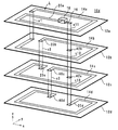
- FIG. 5 is an exploded perspective view of the wireless IC device 10b according to the second embodiment.
- the x-axis is the long side direction of the wireless IC device 10b
- the y-axis is the short side direction of the wireless IC device 10b
- the z-axis is the stacking direction of the wireless IC device 10b.
- FIG. 6 is a cross-sectional structure diagram of the wireless IC device 10b in the zy plane. 5 and 6, the same components as those in FIGS. 1 and 2 are denoted by the same reference numerals.
- the difference between the wireless IC device 10a and the wireless IC device 10b is that the coil electrodes 14a and 14d are replaced with coil electrodes 24a and 24d. More specifically, the line widths of the coil electrodes 24a and 24d are formed wider than the line widths of the coil electrodes 14a and 14b. Thereby, the coil electrodes 24a and 24d located at both ends in the z-axis direction have a wider line width than the other coil electrodes 14b and 14c.
- the coil electrodes 24a and 24d cover at least a part of the other coil electrodes 14b and 14c in the line width direction when viewed in plan from the z-axis direction.
- the coil electrode 24a and the coil electrode 14b will be described.
- the coil electrode 14b is provided so that both ends thereof are accommodated in the coil electrode 24a and do not protrude in the line width direction. Thereby, the electric lines of force E10b generated between the coil electrode 24a and the coil electrode 14b are unlikely to protrude from the coil electrode 24a when viewed in plan from the z-axis direction.
- FIG. 6 the coil electrode 14b is provided so that both ends thereof are accommodated in the coil electrode 24a and do not protrude in the line width direction.
- the coil electrodes 24a and 24d cover at least part of the other coil electrodes 14b and 14c when viewed in plan from the z-axis direction.
- This “being at least partially covered” means, for example, that there is a portion ( ⁇ portion in FIG. 5) where the coil electrode 24a is not provided on the upper side in the z-axis direction of the coil electrode 14b.
- 24a means that the coil electrode 14b may not be completely covered.
- the other configuration of the wireless IC device 10b is the same as that of the wireless IC device 10a, and thus the description thereof is omitted.
- FIG. 7 is an exploded perspective view of the wireless IC device 10c according to the third embodiment.
- the x-axis is the long side direction of the wireless IC device 10c
- the y-axis is the short side direction of the wireless IC device 10c
- the z-axis is the stacking direction of the wireless IC device 10c.
- FIG. 8 is a cross-sectional structure diagram of the wireless IC device 10c in the zy plane. 7 and 8, the same components as those in FIGS. 5 and 6 are denoted by the same reference numerals.
- the difference between the wireless IC device 10b and the wireless IC device 10c is that the insulating sheet 12c is not provided and the coil electrode 14b is replaced with the coil electrode 34b.
- the wireless IC device 10b is configured by stacking four insulating sheets 12, whereas the wireless IC device 10c is configured by stacking three insulating sheets 12 as shown in FIG. Has been. Therefore, in the wireless IC device 10c, the number of coil electrodes 14 and 34 is one less than that in the wireless IC device 10b. Therefore, in the wireless IC device 10c, the number of turns of the antenna coil L of the wireless IC device 10c is made equal to the number of turns of the antenna coil L of the wireless IC device 10b by setting the length of the coil electrode 34b to two rounds. Yes.
- the other configuration of the wireless IC device 10c is the same as that of the wireless IC device 10b, and thus the description thereof is omitted.
- the coil electrodes 24a and 24d positioned at both ends in the z-axis direction circulate around the coil axis of the antenna coil L with a length of less than one turn
- the coil electrodes 24a and 24d other than the coil electrodes 24a and 24d can be used.
- the coil electrode 34b may circulate around the coil axis of the antenna coil L with a length of one or more rounds. Since the wireless IC device 10c has the above-described configuration, as described below, it is possible to reduce the variation in the resonance frequency depending on the use situation, and to increase the number of turns of the antenna coil L even with a small number of layers. Is possible.
- the coil electrode 34b circulates around the coil axis a plurality of times as shown in FIG. 7, the coil electrodes 34b are close to each other on the insulating sheet 12b as shown in FIG. Will be lined up. Therefore, when a current flows through the antenna coil L, an electric force line E10c is generated in the vertical direction of the coil electrode 34b in the z-axis direction.
- the coil electrode 34b is not a coil electrode located at both ends in the z-axis direction, there is a sufficient distance from the coil electrode 34b to the outside of the wireless IC device 10c. Therefore, as shown in FIG. 8, the electric lines of force E10c generated between the coil electrodes 34b hardly protrude from the wireless IC device 10c. Therefore, when the wireless IC device 10c is held by a human hand, the capacitance of the antenna coil L is suppressed from changing due to the electric lines of force E10c passing through the human hand.
- the coil electrodes 24a and 24d when the coil electrodes 24a and 24d are viewed in plan from the z-axis direction, at least a part of the other coil electrodes 34b is covered in the line width direction, which will be described below. As described above, it is possible to more effectively suppress the variation in the resonance frequency depending on the usage state of the wireless IC device 10c. More specifically, as shown in FIG. 8, the coil electrode 34 b does not protrude beyond both ends of the coil electrodes 24 a and 24 d (the coil electrode 24 d is not shown in FIG. 8) in the line width direction. It is provided as follows.
- the electric lines of force E10c are shielded by the coil electrodes 24a and 24d and are more effectively suppressed from protruding out of the wireless IC device 10c. As a result, it is possible to more effectively suppress variations in resonance frequency due to the holding state of the wireless IC device 10c. Although electric lines of force are also generated between the coil electrode 24a and the coil electrode 34b, it is difficult to protrude outside the coil electrode 24a as in the first and second embodiments. Can be suppressed.
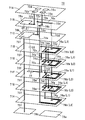
- FIG. 9 is an exploded perspective view of a wireless IC device 10d according to the fourth embodiment.
- the x-axis is the long side direction of the wireless IC device 10d
- the y-axis is the short side direction of the wireless IC device 10d
- the z-axis is the stacking direction of the wireless IC device 10d.
- FIG. 10 is a cross-sectional structure diagram in the zy plane in the vicinity of the connection portion 16 of the wireless IC device 10d. 9 and 10, the same components as those in FIGS. 1 and 2 are denoted by the same reference numerals.
- the difference between the wireless IC device 10a and the wireless IC device 10d is that in the wireless IC device 10d, the coil electrodes 14 are connected by a pouching process instead of being connected by the via-hole conductor b.
- the coil electrodes 14 are connected by a pouching process instead of being connected by the via-hole conductor b.
- the pouching process is a process for connecting two or more electrodes facing each other with an insulating sheet interposed therebetween. Specifically, by pressing a needle or a blade against one electrode, a small hole penetrating the one electrode and the insulating sheet is formed. At this time, the one electrode is plastically deformed so as to reach the other electrode along the inner periphery of the hole. As a result, the two electrodes sandwiching the insulating sheet are connected.
- connection portions 20b, 20c, 20d, 40c, 40d, 42b, and 42c as shown in FIG. .
- the connecting portion 20b is connected to the coil electrode 14b and extends to the inside of the coil electrode 14b so as not to overlap the coil electrodes 14a, 14c, 14d in the z-axis direction.
- the connecting portion 20c is connected to the coil electrode 14c and extends to the inside of the coil electrode 14c so as not to overlap the coil electrodes 14a, 14b, 14d in the z-axis direction.
- the ends of the connection portion 20b and the connection portion 20c overlap in the z-axis direction and are connected by a connection portion c2 formed by pouching processing.
- the connecting portion 40c is connected to the coil electrode 14c and extends to the inside of the coil electrode 14c so as not to overlap the coil electrodes 14a, 14b, 14d in the z-axis direction.
- the connecting portion 40d is connected to the coil electrode 14d and extends to the inside of the coil electrode 14d so as not to overlap the coil electrodes 14a, 14b, 14c in the z-axis direction.
- the ends of the connection part 40c and the connection part 40d overlap in the z-axis direction and are connected by a connection part c3 formed by a pouching process.
- connection portion 16 is connected to the wireless IC 18 on the insulating sheet 12a located on the uppermost side in the z-axis direction. Insulating sheets 12b and 12c other than the insulating sheets 12a and 12d positioned on the uppermost side and the lower side in the z-axis direction so that the connecting parts 42b and 42c overlap with the connecting part 16 when viewed in plan from the z-axis direction. It is provided above. Furthermore, the connecting portion 20d overlaps with the connecting portion 16 and is connected to the coil electrode 14d when viewed in plan from the z-axis direction on the insulating sheet 12d positioned on the lowest side in the z-axis direction. Then, as shown in FIG. 10, the connection portions 16, 42b, 42c, and 20d are collectively placed at the same position when viewed in plan from the z-axis direction by the connection portions c11, c12, and c13 formed by the pouching process. Connected.
- the other configuration of the wireless IC device 10d is the same as that of the wireless IC device 10a, and thus the description thereof is omitted.
- the connecting portions 16, 42b, 42c, and 20d are provided so as to overlap each other when viewed in plan from the z-axis direction. For this reason, it is possible to connect them by a single pouching process. As a result, the manufacturing process of the wireless IC device 10d can be reduced, and the manufacturing cost of the wireless IC device 10d can be reduced.
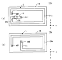
- FIG. 11A is a top view of the wireless IC device 10e according to the fifth embodiment.
- FIG. 11B is a bottom view of the wireless IC device 10e according to the fifth embodiment.
- the x axis is the long side direction of the wireless IC device 10e
- the y axis is the short side direction of the wireless IC device 10e
- the z axis is a direction orthogonal to the x axis and the y axis.
- the wireless IC device according to the embodiment of the present invention does not need to be configured by the plurality of insulating sheets 12. That is, as shown in the wireless IC device 10e shown in FIG. 11, it may be composed of a single insulating sheet 12.
- the wireless IC device 10e will be described below.
- the wireless IC device 10e includes an insulating sheet 12, connection portions 16 and 20a, a wireless IC 18, coil electrodes 54a and 54b, a connection portion 56, and via-hole conductors b21 and b22. Since the insulating sheet 12, the connecting parts 16, 20a, and the wireless IC 18 are the same as the insulating sheet 12, the connecting parts 16, 20a, and the wireless IC 18 of the wireless IC device 10a, description thereof is omitted.
- the coil electrode 54a is formed on the main surface on the upper side in the z-axis direction of the insulating sheet 12, as shown in FIG. As shown in FIG. 11, the coil electrode 54 b is formed on the lower main surface of the insulating sheet 12 in the z-axis direction. That is, the coil electrodes 54a and 54b are provided so as to sandwich the insulating sheet 12.
- the coil electrodes 54a and 54b constitute one ring by overlapping each other when viewed in plan from the z-axis direction.
- the connecting portion 56 is connected to the coil electrode 54b and extends to the inside of the coil electrode 54b.
- the via-hole conductor b21 connects the coil electrode 54a and the coil electrode 54b.
- the via-hole conductor b22 connects the connection part 16 and the connection part 56.
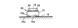
- FIG. 12 is an exploded perspective view of a wireless IC device 10f according to the sixth embodiment.
- the x axis is the long side direction of the wireless IC device 10f
- the y axis is the short side direction of the wireless IC device 10f
- the z axis is the stacking direction of the wireless IC device 10f.
- FIG. 13 is a cross-sectional structure diagram in the xz plane in the vicinity of the electromagnetic coupling module 60 of the wireless IC device 10f.
- FIGS. 12 and 13 the same components as those in FIGS. 1 and 2 are denoted by the same reference numerals.
- the wireless IC 18 is directly connected to the connection units 16 and 20a, whereas in the wireless IC device 10f, as shown in FIG. 12, the wireless IC 18 includes the power supply circuit board 70. Is connected to the connection parts 16 and 20a. In the wireless IC device 10f, the wireless IC 18 and the power supply circuit board 70 constitute an electromagnetic coupling module 60.
- connection electrode 58 is provided on the lower surface of the wireless IC 18.
- the wireless IC 18 is mounted on the power supply circuit board 70 via the connection electrode 58.
- the power supply circuit board 70 includes an inductance element connected to the wireless IC 18 and includes connection electrodes 79a and 79b on the lower surface.
- the connection electrodes 79a and 79b are connected to the connection portions 16 and 20a, respectively.
- FIG. 14 is an exploded perspective view of the feeder circuit board 70.
- the feeder circuit board 70 is formed by laminating, pressing and firing ceramic sheets 71A to 71H made of a dielectric material, and connection electrodes 72a and 72b, electrodes 72c and 72d, and via-hole conductors 73a and 73b are formed on the sheet 71A.
- the ceramic sheet 71B has capacitor electrodes 78a, conductor patterns 75a and 75b, and via-hole conductors 73c to 73e
- the ceramic sheet 71C has capacitor electrodes 78b and via-hole conductors 73d to 73f.
- conductor patterns 76a and 76b and via-hole conductors 73e, 73f, 74a, 74b and 74d are formed on the ceramic sheet 71D
- conductor patterns 76a and 76b and via-hole conductors 73e, 73f, 74a, 74c and 74e are formed on the ceramic sheet 71E.
- the ceramic sheet 71F is formed with capacitor electrodes 77, conductor patterns 76a and 76b, and via-hole conductors 73e, 73f, 74f, and 74g.
- the ceramic sheet 71G is formed with conductor patterns 76a and 76b and via-hole conductors 73e, 73f, and 74f. 74g and conductor patterns 76a and 76b and via-hole conductors 73f are formed on the ceramic sheet 71H.
- the inductance element L1 is configured by the conductor pattern 76a spirally connected by the via-hole conductors 74c, 74d, and 74g, and spirally formed by the via-hole conductors 74b, 74e, and 74f.
- the connected conductor pattern 76b constitutes an inductance element L2
- the capacitor electrodes 78a and 78b constitute a capacitance element C1
- the capacitor electrodes 78b and 77 constitute a capacitance element C2.
- One end of the inductance element L1 is connected to the capacitor electrode 78b via the via-hole conductor 73d, the conductor pattern 75a, and the via-hole conductor 73c, and one end of the inductance element L2 is connected to the capacitor electrode 77 via the via-hole conductor 74a.
- the other ends of the inductance elements L1 and L2 are combined together on the ceramic sheet 71H and connected to the connection electrode 72a via the via-hole conductor 73e, the conductor pattern 75b, and the via-hole conductor 73a.
- the capacitor electrode 78a is electrically connected to the connection electrode 72b through the via-hole conductor 73b.
- connection electrodes 72 a to 72 d are connected to the wireless IC 18 through the connection electrode 58.
- external electrodes 79a and 79b are provided on the lower surface of the feeder circuit board 70 by applying a conductive paste, the external electrode 79a is coupled to the inductance elements L (L1 and L2) by a magnetic field, and the external electrode 79b is a via-hole conductor 73f. Is electrically connected to the capacitor electrode 78b.
- the inductance elements L1 and L2 have a structure in which two conductor patterns 76a and 76b are arranged in parallel.
- the two conductor patterns 76a and 76b have different line lengths, can have different resonance frequencies, and can widen the band of the wireless IC device.
- Each of the ceramic sheets 71A to 71H may be a sheet made of a magnetic ceramic material, and the power supply circuit board 70 may be manufactured by a multilayer substrate manufacturing process such as a conventionally used sheet lamination method or thick film printing method. Can be easily obtained.
- the ceramic sheets 71A to 71H are formed as flexible sheets made of a dielectric material such as polyimide or liquid crystal polymer, and electrodes and conductors are formed on the sheet by a thick film forming method or the like.
- a laminated body may be formed by thermocompression bonding or the like, and inductance elements L1 and L2 and capacitance elements C1 and C2 may be incorporated.
- the inductance elements L1 and L2 and the capacitance elements C1 and C2 are provided at different positions in a plan view, and are coupled magnetically to the external electrode 79a by the inductance elements L1 and L2, and the external electrode 79b is a capacitance. This is one electrode constituting the element C1.
- the electromagnetic coupling module 60 in which the wireless IC 18 is mounted on the power supply circuit board 70 receives a high-frequency signal from a reader / writer (not shown) by the antenna coil L, and magnetically couples with the external electrodes 79a and 79b via the antenna coil L.
- the resonance circuit is resonated, and only a reception signal in a predetermined frequency band is supplied to the wireless IC 18.
- a predetermined energy is extracted from the received signal, and information stored in the wireless IC 18 using this energy as a drive source is matched with a predetermined frequency by a resonance circuit, and then the external electrodes 79a and 79b and the antenna coil L are matched.
- the data is transmitted to the reader / writer via.
- the resonance frequency characteristic is determined by a resonance circuit composed of the inductance elements L1 and L2 and the capacitance elements C1 and C2.
- the frequency of the signal from the antenna coil L is substantially determined by the self-resonance frequency of the resonance circuit.
- the other configuration of the wireless IC device 10f is the same as that of the wireless IC device 10a, and thus the description thereof is omitted.
- the power supply circuit board 70 can also be applied to the wireless IC devices 10b to 10e other than the wireless IC device 10a.
- FIG. 15 is an exploded perspective view of a wireless IC device 10g according to the seventh embodiment.
- the x-axis is the long side direction of the wireless IC device 10g
- the y-axis is the short side direction of the wireless IC device 10g
- the z-axis is the stacking direction of the wireless IC device 10g.
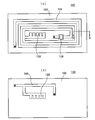
- FIG. 16A is a cross-sectional structure diagram in the zy plane in the vicinity of the wireless IC of the wireless IC device according to the reference example
- FIG. 16B is a cross-sectional structure diagram in the zy plane in the vicinity of the wireless IC 18 of the wireless IC device 10g. It is. 15 and FIG. 16, the same reference numerals are assigned to the same components as those in FIG. 1 and FIG.
- the difference between the wireless IC device 10a and the wireless IC device 10g is that, in the wireless IC device 10g, the wireless IC 18 has one ring formed of a plurality of coil electrodes 14a to 14c when viewed in plan from the z-axis direction. It is the point provided so that it may overlap. The following points will be described.
- the wireless IC 18 is provided so as to overlap with one ring formed by the plurality of coil electrodes 14a to 14c when viewed in plan from the z-axis direction. Therefore, the wireless IC 18 is connected to one end of the coil electrode 14a.
- connection portion 16 is provided so as to overlap with one ring formed by the plurality of coil electrodes 14a to 14c, and is connected to the wireless IC 18.
- the other end of the connection portion 16 is drawn into the one ring and is connected to the connection portion 20c via the via-hole conductors b11 and b12.
- the other configuration of the wireless IC device 10g is the same as that of the wireless IC device 10a, and thus the description thereof is omitted.
- the wireless IC device 10g when the insulating sheet 12 is bent, a load on the wireless IC 18 is suppressed. More specifically, since the insulating sheet 12 is a flexible sheet, it may be bent during use. Since the wireless IC 18 is composed of a semiconductor substrate, the wireless IC 18 is harder than the insulating sheet 12. Therefore, when the insulating sheet 12 is bent, the stress may be concentrated on the wireless IC 18 and the connecting portion between the wireless IC 18 and the antenna coil L, or the wireless IC 18 may be damaged, or the wireless IC 18 may be disconnected from the antenna coil L. May come off.
- the wireless IC 18 is provided so as to overlap with one ring formed by the coil electrodes 14a to 14c.
- the one ring is less likely to bend than the other part of the wireless IC device 10g because the coil electrodes 14a to 14c overlap each other. Therefore, even if the insulating sheet 12 is bent, the portion where the wireless IC 18 is provided is suppressed from being bent greatly. As a result, it is possible to suppress the load from being applied to the wireless IC 18 and the connection portion between the wireless IC 18 and the antenna coil L.
- the magnetic field is less likely to be disturbed as will be described below. More specifically, the magnetic field is generated so as to circulate around the coil electrode 14. Therefore, when the wireless IC 18 is provided so as not to overlap with the coils 14a to 14c when seen in a plan view from the z-axis direction, the wireless IC 18 has a coil shape like the wireless IC device according to the reference example shown in FIG. The magnetic field generated by the electrode 14 is hindered. That is, in the wireless IC device according to the reference example, the magnetic flux is disturbed.
- the wireless IC 18 is provided so as to overlap the coil electrodes 14a to 14c when viewed in plan from the z-axis direction. Therefore, as shown in FIG. 16B, the magnetic field is generated so as to circulate around the coil electrodes 14a to 14c and the wireless IC 18. Therefore, the wireless IC 18 does not disturb the magnetic field. As a result, in the wireless IC device 10g, the magnetic field is hardly disturbed.
- the wireless IC device according to the embodiment of the present invention is not limited to the wireless IC devices 10a to 10g described in the first to seventh embodiments, and can be changed within the scope of the gist thereof.
- the coil electrode 14 has a length of less than one turn means that the length is substantially less than one turn. Therefore, it is allowed that the length of the coil electrode 14 slightly exceeds one round so that the resonance frequency of the wireless IC device 10 does not vary depending on the use situation.
- the human hand touched the wireless IC device 10 as a cause of the resonance frequency variation
- the cause of the resonance frequency variation is not limited to this.
- the wireless IC device 10 is used in a card case or the like
- the resonance frequency varies also when the card case or the like touches the wireless IC device 10.
- the shape of the insulating sheet 12 is not necessarily rectangular, but it is preferable that no large hole or notch is formed inside the antenna coil L. If a large hole or notch is provided inside the antenna coil L in the insulating sheet 12, for example, the human hand Fin3 approaches from the left side of FIG. This is because the line E10a may pass through a human hand.
- the coil electrodes 14, 24, and 34 are provided so as to coincide with the line width direction when viewed in plan from the z-axis direction.
- the lower coil electrodes 14, 24, and 34 in the z-axis direction may slightly protrude from the upper coil electrodes 14, 24, and 34 in the z-axis direction when viewed in plan from the z-axis direction.
- the amount of protrusion of the coil electrodes 14, 24, and 34 needs to be an extent that does not affect the resonance frequency.
- the coil electrode 14a located on the uppermost side in the z-axis direction is separated from the coil electrodes 14a to 14d with the insulating sheet 12 sandwiched in the passage region of the ring constituted by the coil electrodes 14a to 14d. Do not line up. This is because, when the coil electrodes 14 are arranged as shown in FIG. 17, electric lines of force that protrude outside the wireless IC device 10 a are generated between the coil electrodes 14.
- the coil electrode 14d positioned on the lowermost side in the z-axis direction has an insulating sheet inside the ring formed by the coil electrodes 14a to 14d. 12, the coil electrodes 14a to 14d should not be arranged apart from each other.
- the wireless IC device 10a has been described as an example, but the same applies to the wireless IC devices 10b to 10g.
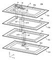
- FIG. 18 is an exploded perspective view of the wireless IC card 80.
- an insulating sheet 12 made of glass epoxy base, polyimide, vinyl chloride, polyethylene terephthalate (PET), PET-G, liquid crystal polymer resin or the like.
- a coil electrode 14 shown in FIG. 9 is formed on each of the insulating sheets 12.
- the coil electrode 14 is a copper foil, the coil electrode 14 is formed by, for example, an etching process.
- the connecting portions 16, 20a, 20b, 20c, 20d, 40c, 40d, 42b, and 42c are also formed by, for example, an etching process. More specifically, the connection portion 20a connected to the coil electrode 14a is formed on the insulating sheet 12a, and the connection portion 16 is formed at a position away from the connection portion 20a by the region where the wireless IC 18 is mounted. Further, when the insulating sheets 12a to 12d are stacked on the insulating sheets 12b and 12c, the connecting portions 42b and 42c are formed so as to overlap the connecting portion 16 when viewed in plan from the z-axis direction.
- connection portions 20b and 20c connected to the coil electrodes 14b and 14c are formed simultaneously with the formation of the connection portions 42b and 42c.
- a connection portion 20d that overlaps with the connection portion 16 and is connected to the coil electrode 14d when viewed in plan from the z-axis direction is formed on the insulating sheet 12d.
- a connection portion 40d connected to the coil electrode 14d is formed simultaneously with the formation of the connection portion 20d.
- the coil electrodes 14a to 14d and the connecting portions 16, 20a, 20b, 20c, 20d, 40c, 40d, 42b, and 42c can be formed by a screen printing method in which a conductive paste is applied.
- the plurality of insulating sheets 12a to 12d are aligned and laminated so that the plurality of coil electrodes 14a to 14d overlap to form one ring.
- the connecting portions 16, 42b, 42c, and 20d also overlap each other.
- connection portion 16 the connection portion 42b, the connection portion 42c, and the connection portion 20d are pouched. Connecting. At this time, since the connection portion 16, the connection portion 42b, the connection portion 42c, and the connection portion 20d overlap when viewed in plan from the z-axis direction, they are collectively connected by a single pouching process.
- the wireless IC 18 is mounted on the connection portions 16 and 20a of the insulating sheet 12a. Specifically, the wireless IC 18 is mounted by a flip chip mounting method using an anisotropic conductive film (ACF). At this time, alignment is performed so that the wireless IC 18 is connected to the connection portions 16 and 20a, and temporary bonding is performed, and then the wireless IC 18 is permanently bonded by applying heat pressure.
- the wireless IC device 10d is completed through the above steps.
- the wireless IC card 80 is manufactured by attaching the overlay sheets 82a and 82b using the adhesive sheets 84a and 84b as shown in FIG. More specifically, the adhesive sheet 84a and the overlay sheet 82a are stacked on the upper side of the wireless IC device 10d in the z-axis direction, and the adhesive sheet 84b and the overlay sheet 82b are stacked on the lower side of the wireless IC device 10d. And these are heated and pressure-bonded. Thereby, the wireless IC card 80 is completed.
- the wireless IC devices 10a to 10c can be manufactured by substantially the same manufacturing method.
- the coil electrodes 14, 24, and 34 are connected not by the pouching process but by the via-hole conductor b. Therefore, a step of forming the via-hole conductor b is performed on each insulating sheet 12 instead of the step of performing the pouching process.
- the via hole conductor b is formed by irradiating the insulating sheet 12 with a laser beam to form a via hole and filling the via hole with a conductive paste.
- the conductive paste is applied to the insulating sheet 12 simultaneously with the step of filling the via holes with the conductive paste, and the coil electrodes 14, 24, 34 can be formed.
- an electromagnetic coupling module 60 including the wireless IC 18 and the power feeding circuit board 70 is mounted instead of the wireless IC 18.
- the present invention is useful for a wireless IC device and a method for manufacturing the same, and is particularly excellent in that the resonance frequency can be reduced from varying depending on use conditions.
- Electromagnetic coupling module 70 Power supply circuit board 80 Wireless IC card
Abstract
Priority Applications (4)
| Application Number | Priority Date | Filing Date | Title |
|---|---|---|---|
| JP2010513041A JP4661994B2 (ja) | 2008-05-22 | 2009-05-20 | 無線icデバイス及びその製造方法 |
| EP09750597.8A EP2280449B1 (fr) | 2008-05-22 | 2009-05-20 | Dispositif ci sans fil et son procédé de fabrication |
| CN200980118906.0A CN102037607B (zh) | 2008-05-22 | 2009-05-20 | 无线ic器件及其制造方法 |
| US12/940,103 US8047445B2 (en) | 2008-05-22 | 2010-11-05 | Wireless IC device and method of manufacturing the same |
Applications Claiming Priority (4)
| Application Number | Priority Date | Filing Date | Title |
|---|---|---|---|
| JP2008133829 | 2008-05-22 | ||
| JP2008-133829 | 2008-05-22 | ||
| JPPCT/JP2009/056698 | 2009-03-31 | ||
| PCT/JP2009/056698 WO2009142068A1 (fr) | 2008-05-22 | 2009-03-31 | Dispositif à circuit intégré sans fil et son procédé de fabrication |
Related Child Applications (1)
| Application Number | Title | Priority Date | Filing Date |
|---|---|---|---|
| PCT/JP2009/056698 Continuation WO2009142068A1 (fr) | 2008-05-22 | 2009-03-31 | Dispositif à circuit intégré sans fil et son procédé de fabrication |
Publications (1)
| Publication Number | Publication Date |
|---|---|
| WO2009142235A1 true WO2009142235A1 (fr) | 2009-11-26 |
Family
ID=41340007
Family Applications (3)
| Application Number | Title | Priority Date | Filing Date |
|---|---|---|---|
| PCT/JP2009/056698 WO2009142068A1 (fr) | 2008-05-22 | 2009-03-31 | Dispositif à circuit intégré sans fil et son procédé de fabrication |
| PCT/JP2009/059259 WO2009142235A1 (fr) | 2008-05-22 | 2009-05-20 | Dispositif ci sans fil et son procédé de fabrication |
| PCT/JP2009/059410 WO2009142288A1 (fr) | 2008-05-22 | 2009-05-22 | Dispositif ci sans fil |
Family Applications Before (1)
| Application Number | Title | Priority Date | Filing Date |
|---|---|---|---|
| PCT/JP2009/056698 WO2009142068A1 (fr) | 2008-05-22 | 2009-03-31 | Dispositif à circuit intégré sans fil et son procédé de fabrication |
Family Applications After (1)
| Application Number | Title | Priority Date | Filing Date |
|---|---|---|---|
| PCT/JP2009/059410 WO2009142288A1 (fr) | 2008-05-22 | 2009-05-22 | Dispositif ci sans fil |
Country Status (5)
| Country | Link |
|---|---|
| US (2) | US7967216B2 (fr) |
| EP (1) | EP2280449B1 (fr) |
| JP (2) | JP4661994B2 (fr) |
| CN (2) | CN102037607B (fr) |
| WO (3) | WO2009142068A1 (fr) |
Cited By (7)
| Publication number | Priority date | Publication date | Assignee | Title |
|---|---|---|---|---|
| WO2011157693A1 (fr) * | 2010-06-18 | 2011-12-22 | Fci | Circuit imprimé multi-couche souple et son procédé de fabrication |
| WO2012020073A3 (fr) * | 2010-08-12 | 2012-05-24 | Féinics Amatech Teoranta Limited | Modules d'antenne rfid et amélioration de couplage |
| CN102668241A (zh) * | 2010-03-24 | 2012-09-12 | 株式会社村田制作所 | Rfid系统 |
| US8474726B2 (en) | 2010-08-12 | 2013-07-02 | Feinics Amatech Teoranta | RFID antenna modules and increasing coupling |
| US8991712B2 (en) | 2010-08-12 | 2015-03-31 | Féinics Amatech Teoranta | Coupling in and to RFID smart cards |
| US9033250B2 (en) | 2010-08-12 | 2015-05-19 | Féinics Amatech Teoranta | Dual interface smart cards, and methods of manufacturing |
| JP2019008596A (ja) * | 2017-06-26 | 2019-01-17 | 京セラ株式会社 | 配線基板およびrfidタグ |
Families Citing this family (77)
| Publication number | Priority date | Publication date | Assignee | Title |
|---|---|---|---|---|
| US7519328B2 (en) * | 2006-01-19 | 2009-04-14 | Murata Manufacturing Co., Ltd. | Wireless IC device and component for wireless IC device |
| US9306358B2 (en) | 2009-03-09 | 2016-04-05 | Nucurrent, Inc. | Method for manufacture of multi-layer wire structure for high efficiency wireless communication |
| US9208942B2 (en) * | 2009-03-09 | 2015-12-08 | Nucurrent, Inc. | Multi-layer-multi-turn structure for high efficiency wireless communication |
| US9232893B2 (en) | 2009-03-09 | 2016-01-12 | Nucurrent, Inc. | Method of operation of a multi-layer-multi-turn structure for high efficiency wireless communication |
| US9439287B2 (en) | 2009-03-09 | 2016-09-06 | Nucurrent, Inc. | Multi-layer wire structure for high efficiency wireless communication |
| US9300046B2 (en) * | 2009-03-09 | 2016-03-29 | Nucurrent, Inc. | Method for manufacture of multi-layer-multi-turn high efficiency inductors |
| WO2010104569A1 (fr) | 2009-03-09 | 2010-09-16 | Neurds Inc. | Système et procédé pour le transfert d'énergie sans fil dans des dispositifs médicaux aptes à être implantés |
| US11476566B2 (en) | 2009-03-09 | 2022-10-18 | Nucurrent, Inc. | Multi-layer-multi-turn structure for high efficiency wireless communication |
| US9444213B2 (en) | 2009-03-09 | 2016-09-13 | Nucurrent, Inc. | Method for manufacture of multi-layer wire structure for high efficiency wireless communication |
| JP5287485B2 (ja) * | 2009-05-11 | 2013-09-11 | 富士ゼロックス株式会社 | 情報表現画像、印刷物、画像処理装置及び画像処理プログラム |
| JP2011238016A (ja) * | 2010-05-10 | 2011-11-24 | Sony Corp | 非接触通信媒体、アンテナパターン配置媒体、通信装置及びアンテナ調整方法 |
| JP5234084B2 (ja) * | 2010-11-05 | 2013-07-10 | 株式会社村田製作所 | アンテナ装置および通信端末装置 |
| CN102799909A (zh) * | 2011-06-24 | 2012-11-28 | 深圳光启高等理工研究院 | 读写器、电子标签和射频识别系统 |
| JP5790200B2 (ja) * | 2011-06-27 | 2015-10-07 | ソニー株式会社 | 通信装置並びに通信システム |
| US9634391B2 (en) | 2011-08-08 | 2017-04-25 | Féinics Amatech Teoranta | RFID transponder chip modules |
| US9622359B2 (en) | 2011-08-08 | 2017-04-11 | Féinics Amatech Teoranta | RFID transponder chip modules |
| US9489613B2 (en) | 2011-08-08 | 2016-11-08 | Féinics Amatech Teoranta | RFID transponder chip modules with a band of the antenna extending inward |
| DE102011056326B4 (de) * | 2011-12-13 | 2019-04-04 | Infineon Technologies Ag | Chipkarten-Kontaktfeld-Anordnung |
| US8890751B2 (en) * | 2012-02-17 | 2014-11-18 | Pinyon Technologies, Inc. | Antenna having a planar conducting element with first and second end portions separated by a non-conductive gap |
| KR101859575B1 (ko) * | 2012-03-21 | 2018-05-18 | 삼성전자 주식회사 | 근거리무선통신 안테나 장치 및 이를 구비하는 전자기기 |
| CN102663486B (zh) * | 2012-04-04 | 2016-03-30 | 上海仪电智能电子有限公司 | 一种微型智能标签 |
| JP5505571B2 (ja) * | 2012-04-27 | 2014-05-28 | 株式会社村田製作所 | コイルアンテナおよび通信端末装置 |
| WO2014045518A1 (fr) * | 2012-09-18 | 2014-03-27 | パナソニック株式会社 | Antenne, dispositif d'envoi, dispositif de réception, circuit intégré tridimensionnel, et système de communication sans contact |
| US9202162B2 (en) * | 2012-11-09 | 2015-12-01 | Maxim Integrated Products, Inc. | Embedded radio frequency identification (RFID) package |
| WO2014083916A1 (fr) * | 2012-11-30 | 2014-06-05 | 株式会社村田製作所 | Module d'antenne |
| JP5655987B2 (ja) * | 2012-12-07 | 2015-01-21 | 株式会社村田製作所 | アンテナモジュール |
| CN103050779B (zh) * | 2013-01-24 | 2015-10-28 | 青岛歌尔声学科技有限公司 | 一种nfc天线及其制造方法和一种nfc通信设备 |
| US9197277B2 (en) * | 2014-01-13 | 2015-11-24 | Tyco Fire & Security Gmbh | Two-way wireless communication enabled intrusion detector assemblies |
| US9196137B2 (en) | 2014-01-13 | 2015-11-24 | Tyco Fire & Security Gmbh | Two-way wireless communication enabled intrusion detector assemblies |
| WO2015128188A2 (fr) * | 2014-02-27 | 2015-09-03 | Féinics Amatech Teoranta | Modules de puce rfid de transpondeur |
| US10839282B2 (en) | 2014-03-08 | 2020-11-17 | Féinics Amatech Teoranta | RFID transponder chip modules, elements thereof, and methods |
| CN106233310B (zh) * | 2014-12-19 | 2019-05-10 | 株式会社村田制作所 | 无线ic器件、树脂成型体及其制造方法 |
| WO2016120254A1 (fr) * | 2015-01-27 | 2016-08-04 | At & S Austria Technologie & Systemtechnik Aktiengesellschaft | Porte-composant avec structure d'antenne integrée |
| DE102015003784A1 (de) * | 2015-03-23 | 2016-09-29 | Dieter Kilian | Antenne für Nahbereichsanwendungen sowie Verwendung einer derartigen Antenne |
| US9807704B2 (en) | 2015-03-30 | 2017-10-31 | Ford Global Technologies, Llc | Key fob transmission compensation |
| US9865111B2 (en) * | 2015-03-30 | 2018-01-09 | Ford Global Technologies, Llc | Fob case for reduced transmission interference |
| USD812598S1 (en) * | 2015-06-17 | 2018-03-13 | Inside Secure | Data communication antenna |
| US10636563B2 (en) | 2015-08-07 | 2020-04-28 | Nucurrent, Inc. | Method of fabricating a single structure multi mode antenna for wireless power transmission using magnetic field coupling |
| US9941590B2 (en) | 2015-08-07 | 2018-04-10 | Nucurrent, Inc. | Single structure multi mode antenna for wireless power transmission using magnetic field coupling having magnetic shielding |
| US9960628B2 (en) | 2015-08-07 | 2018-05-01 | Nucurrent, Inc. | Single structure multi mode antenna having a single layer structure with coils on opposing sides for wireless power transmission using magnetic field coupling |
| US9941743B2 (en) | 2015-08-07 | 2018-04-10 | Nucurrent, Inc. | Single structure multi mode antenna having a unitary body construction for wireless power transmission using magnetic field coupling |
| US9941729B2 (en) | 2015-08-07 | 2018-04-10 | Nucurrent, Inc. | Single layer multi mode antenna for wireless power transmission using magnetic field coupling |
| US11205848B2 (en) | 2015-08-07 | 2021-12-21 | Nucurrent, Inc. | Method of providing a single structure multi mode antenna having a unitary body construction for wireless power transmission using magnetic field coupling |
| US10063100B2 (en) | 2015-08-07 | 2018-08-28 | Nucurrent, Inc. | Electrical system incorporating a single structure multimode antenna for wireless power transmission using magnetic field coupling |
| US10658847B2 (en) | 2015-08-07 | 2020-05-19 | Nucurrent, Inc. | Method of providing a single structure multi mode antenna for wireless power transmission using magnetic field coupling |
| US9960629B2 (en) | 2015-08-07 | 2018-05-01 | Nucurrent, Inc. | Method of operating a single structure multi mode antenna for wireless power transmission using magnetic field coupling |
| US9948129B2 (en) | 2015-08-07 | 2018-04-17 | Nucurrent, Inc. | Single structure multi mode antenna for wireless power transmission using magnetic field coupling having an internal switch circuit |
| US10985465B2 (en) | 2015-08-19 | 2021-04-20 | Nucurrent, Inc. | Multi-mode wireless antenna configurations |
| EP3166181A1 (fr) * | 2015-11-05 | 2017-05-10 | Gemalto Sa | Procede de fabrication d'antenne radiofrequence sur un support et antenne ainsi obtenue |
| JP6573199B2 (ja) * | 2016-02-04 | 2019-09-11 | パナソニックIpマネジメント株式会社 | 無線電力伝送システムおよび送電装置 |
| EP4340012A2 (fr) | 2016-04-28 | 2024-03-20 | AT & S Austria Technologie & Systemtechnik Aktiengesellschaft | Support de composant avec agencement d'antenne intégré, appareil électronique, procédé de communication radio |
| US10879704B2 (en) | 2016-08-26 | 2020-12-29 | Nucurrent, Inc. | Wireless connector receiver module |
| CN106503784A (zh) * | 2016-10-10 | 2017-03-15 | 杭州潮盛科技有限公司 | Rfid标签及其制作工艺 |
| EP3552298A4 (fr) | 2016-12-09 | 2020-01-15 | NuCurrent, Inc. | Substrat configuré pour faciliter un transfert d'énergie par métal par l'intermédiaire d'un couplage magnétique en champ proche |
| US10958105B2 (en) | 2017-02-13 | 2021-03-23 | Nucurrent, Inc. | Transmitting base with repeater |
| WO2018179045A1 (fr) | 2017-03-27 | 2018-10-04 | 三菱電機株式会社 | Sonde de champ électromagnétique |
| JP6555444B2 (ja) * | 2017-03-27 | 2019-08-07 | 株式会社村田製作所 | アンテナ装置 |
| KR102312002B1 (ko) * | 2017-04-12 | 2021-10-13 | 주식회사 위츠 | 무선 통신 안테나 및 그를 이용한 무선 통신 장치 |
| JP6485608B1 (ja) * | 2017-04-28 | 2019-03-20 | 株式会社村田製作所 | Rfidタグ |
| US11282638B2 (en) | 2017-05-26 | 2022-03-22 | Nucurrent, Inc. | Inductor coil structures to influence wireless transmission performance |
| FR3073307B1 (fr) * | 2017-11-08 | 2021-05-28 | Oberthur Technologies | Dispositif de securite tel qu'une carte a puce |
| JP7233893B2 (ja) * | 2017-11-21 | 2023-03-07 | 台湾東電化股▲ふん▼有限公司 | 無線装置 |
| CN109492741A (zh) * | 2018-11-26 | 2019-03-19 | 昆山联滔电子有限公司 | 一种电子模组及电子装置 |
| CN111313150A (zh) * | 2018-12-11 | 2020-06-19 | 航天信息股份有限公司 | 一种rfid天线 |
| WO2020255791A1 (fr) * | 2019-06-18 | 2020-12-24 | 凸版印刷株式会社 | Carte de câblage multicouche ayant un circuit de résonance lc, et boîtier de composant électronique utilisant une carte de câblage multicouche ayant un circuit de résonance lc |
| US11271430B2 (en) | 2019-07-19 | 2022-03-08 | Nucurrent, Inc. | Wireless power transfer system with extended wireless charging range |
| US11227712B2 (en) | 2019-07-19 | 2022-01-18 | Nucurrent, Inc. | Preemptive thermal mitigation for wireless power systems |
| US10977539B1 (en) * | 2019-12-20 | 2021-04-13 | Capital One Services, Llc | Systems and methods for use of capacitive member to prevent chip fraud |
| US11056922B1 (en) | 2020-01-03 | 2021-07-06 | Nucurrent, Inc. | Wireless power transfer system for simultaneous transfer to multiple devices |
| US11283303B2 (en) | 2020-07-24 | 2022-03-22 | Nucurrent, Inc. | Area-apportioned wireless power antenna for maximized charging volume |
| USD943024S1 (en) | 2020-07-30 | 2022-02-08 | Federal Card Services, LLC | Asymmetrical arrangement of contact pads and connection bridges of a transponder chip module |
| USD942538S1 (en) | 2020-07-30 | 2022-02-01 | Federal Card Services, LLC | Asymmetrical arrangement of contact pads and connection bridges of a transponder chip module |
| JP2022099098A (ja) * | 2020-12-22 | 2022-07-04 | 富士フイルム株式会社 | 非接触式通信媒体 |
| US11881716B2 (en) | 2020-12-22 | 2024-01-23 | Nucurrent, Inc. | Ruggedized communication for wireless power systems in multi-device environments |
| US11876386B2 (en) | 2020-12-22 | 2024-01-16 | Nucurrent, Inc. | Detection of foreign objects in large charging volume applications |
| US11695302B2 (en) | 2021-02-01 | 2023-07-04 | Nucurrent, Inc. | Segmented shielding for wide area wireless power transmitter |
| US11831174B2 (en) | 2022-03-01 | 2023-11-28 | Nucurrent, Inc. | Cross talk and interference mitigation in dual wireless power transmitter |
Citations (4)
| Publication number | Priority date | Publication date | Assignee | Title |
|---|---|---|---|---|
| JPH10193851A (ja) * | 1997-01-08 | 1998-07-28 | Denso Corp | 非接触カード |
| JP2001010264A (ja) | 1999-07-02 | 2001-01-16 | Dainippon Printing Co Ltd | 非接触型icカードとそのアンテナ特性調整方法 |
| JP2006042097A (ja) * | 2004-07-29 | 2006-02-09 | Kyocera Corp | アンテナ配線基板 |
| JP2008072243A (ja) * | 2006-09-12 | 2008-03-27 | Murata Mfg Co Ltd | 無線icデバイス |
Family Cites Families (288)
| Publication number | Priority date | Publication date | Assignee | Title |
|---|---|---|---|---|
| US3364564A (en) * | 1965-06-28 | 1968-01-23 | Gregory Ind Inc | Method of producing welding studs dischargeable in end-to-end relationship |
| JPS6193701A (ja) * | 1984-10-13 | 1986-05-12 | Toyota Motor Corp | 自動車用アンテナ装置 |
| US5253969A (en) * | 1989-03-10 | 1993-10-19 | Sms Schloemann-Siemag Aktiengesellschaft | Feeding system for strip material, particularly in treatment plants for metal strips |
| JP2763664B2 (ja) * | 1990-07-25 | 1998-06-11 | 日本碍子株式会社 | 分布定数回路用配線基板 |
| NL9100176A (nl) | 1991-02-01 | 1992-03-02 | Nedap Nv | Antenne met transformator voor contactloze informatieoverdracht vanuit integrated circuit-kaart. |
| NL9100347A (nl) | 1991-02-26 | 1992-03-02 | Nedap Nv | Geintegreerde transformator voor een contactloze identificatiekaart. |
| JPH04321190A (ja) * | 1991-04-22 | 1992-11-11 | Mitsubishi Electric Corp | 非接触型携帯記憶装置のアンテナ回路 |
| EP0522806B1 (fr) * | 1991-07-08 | 1996-11-20 | Nippon Telegraph And Telephone Corporation | Système d'antenne rétractable |
| US5491483A (en) * | 1994-01-05 | 1996-02-13 | Texas Instruments Incorporated | Single loop transponder system and method |
| US6096431A (en) | 1994-07-25 | 2000-08-01 | Toppan Printing Co., Ltd. | Biodegradable cards |
| JP3141692B2 (ja) * | 1994-08-11 | 2001-03-05 | 松下電器産業株式会社 | ミリ波用検波器 |
| US5528222A (en) * | 1994-09-09 | 1996-06-18 | International Business Machines Corporation | Radio frequency circuit and memory in thin flexible package |
| US5955723A (en) * | 1995-05-03 | 1999-09-21 | Siemens Aktiengesellschaft | Contactless chip card |
| US5629241A (en) * | 1995-07-07 | 1997-05-13 | Hughes Aircraft Company | Microwave/millimeter wave circuit structure with discrete flip-chip mounted elements, and method of fabricating the same |
| JP3150575B2 (ja) * | 1995-07-18 | 2001-03-26 | 沖電気工業株式会社 | タグ装置及びその製造方法 |
| GB2305075A (en) | 1995-09-05 | 1997-03-26 | Ibm | Radio Frequency Tag for Electronic Apparatus |
| DE19534229A1 (de) * | 1995-09-15 | 1997-03-20 | Licentia Gmbh | Transponderanordnung |
| AUPO055296A0 (en) * | 1996-06-19 | 1996-07-11 | Integrated Silicon Design Pty Ltd | Enhanced range transponder system |
| US6104311A (en) | 1996-08-26 | 2000-08-15 | Addison Technologies | Information storage and identification tag |
| JP2001505682A (ja) | 1996-10-09 | 2001-04-24 | ペーアーファウ カード ゲームベーハ | スマートカードの製造方法及び製造のための接続配置 |
| JPH10193849A (ja) | 1996-12-27 | 1998-07-28 | Rohm Co Ltd | 回路チップ搭載カードおよび回路チップモジュール |
| DE19703029A1 (de) | 1997-01-28 | 1998-07-30 | Amatech Gmbh & Co Kg | Übertragungsmodul für eine Transpondervorrichtung sowie Transpondervorrichtung und Verfahren zum Betrieb einer Transpondervorrichtung |
| US6181287B1 (en) * | 1997-03-10 | 2001-01-30 | Precision Dynamics Corporation | Reactively coupled elements in circuits on flexible substrates |
| EP1031939B1 (fr) * | 1997-11-14 | 2005-09-14 | Toppan Printing Co., Ltd. | Carte ci composite |
| JPH11261325A (ja) * | 1998-03-10 | 1999-09-24 | Shiro Sugimura | コイル素子と、その製造方法 |
| US6362784B1 (en) * | 1998-03-31 | 2002-03-26 | Matsuda Electric Industrial Co., Ltd. | Antenna unit and digital television receiver |
| US5936150A (en) * | 1998-04-13 | 1999-08-10 | Rockwell Science Center, Llc | Thin film resonant chemical sensor with resonant acoustic isolator |
| CA2293228A1 (fr) | 1998-04-14 | 1999-10-21 | Robert A. Katchmazenski | Contenant pour compresseurs et autres marchandises |
| US6018299A (en) | 1998-06-09 | 2000-01-25 | Motorola, Inc. | Radio frequency identification tag having a printed antenna and method |
| US6107920A (en) * | 1998-06-09 | 2000-08-22 | Motorola, Inc. | Radio frequency identification tag having an article integrated antenna |
| JP2000021639A (ja) | 1998-07-02 | 2000-01-21 | Sharp Corp | インダクター、これを用いた共振回路、整合回路、アンテナ回路及び発振回路 |
| JP2000022421A (ja) * | 1998-07-03 | 2000-01-21 | Murata Mfg Co Ltd | チップアンテナ及びそれを搭載した無線機器 |
| JP2000311226A (ja) | 1998-07-28 | 2000-11-07 | Toshiba Corp | 無線icカード及びその製造方法並びに無線icカード読取り書込みシステム |
| EP0977145A3 (fr) | 1998-07-28 | 2002-11-06 | Kabushiki Kaisha Toshiba | Carte à puce radio |
| JP2000059260A (ja) | 1998-08-04 | 2000-02-25 | Sony Corp | 記憶装置 |
| CA2338522C (fr) | 1998-08-14 | 2009-04-07 | 3M Innovative Properties Company | Applications pour des systemes d'identification de frequence radio |
| EP1298573A3 (fr) * | 1998-08-14 | 2003-09-17 | 3M Innovative Properties Company | Système d'identification radio fréquence comprenant plusieurs antennes |
| JP4411670B2 (ja) | 1998-09-08 | 2010-02-10 | 凸版印刷株式会社 | 非接触icカードの製造方法 |
| JP4508301B2 (ja) | 1998-09-16 | 2010-07-21 | 大日本印刷株式会社 | 非接触icカード |
| JP3632466B2 (ja) | 1998-10-23 | 2005-03-23 | 凸版印刷株式会社 | 非接触icカード用の検査装置および検査方法 |
| JP3924962B2 (ja) | 1998-10-30 | 2007-06-06 | 株式会社デンソー | 皿状物品用idタグ |
| JP2000137779A (ja) | 1998-10-30 | 2000-05-16 | Hitachi Maxell Ltd | 非接触情報媒体とその製造方法 |
| US6837438B1 (en) * | 1998-10-30 | 2005-01-04 | Hitachi Maxell, Ltd. | Non-contact information medium and communication system utilizing the same |
| JP2000137785A (ja) | 1998-10-30 | 2000-05-16 | Sony Corp | 非接触型icカードの製造方法および非接触型icカード |
| JP2000148948A (ja) | 1998-11-05 | 2000-05-30 | Sony Corp | 非接触型icラベルおよびその製造方法 |
| JP2000172812A (ja) | 1998-12-08 | 2000-06-23 | Hitachi Maxell Ltd | 非接触情報媒体 |
| JP3088404B2 (ja) | 1999-01-14 | 2000-09-18 | 埼玉日本電気株式会社 | 移動無線端末および内蔵アンテナ |
| JP2000222540A (ja) | 1999-02-03 | 2000-08-11 | Hitachi Maxell Ltd | 非接触型半導体タグ |
| JP2000228602A (ja) * | 1999-02-08 | 2000-08-15 | Alps Electric Co Ltd | 共振線路 |
| JP2000243797A (ja) | 1999-02-18 | 2000-09-08 | Sanken Electric Co Ltd | 半導体ウエハ及びその切断法並びに半導体ウエハ組立体及びその切断法 |
| JP3967487B2 (ja) | 1999-02-23 | 2007-08-29 | 株式会社東芝 | Icカード |
| JP2000251049A (ja) | 1999-03-03 | 2000-09-14 | Konica Corp | カード及びその製造方法 |
| JP4106673B2 (ja) * | 1999-03-05 | 2008-06-25 | 株式会社エフ・イー・シー | コイルユニットを使用するアンテナ装置、プリント回路基板 |
| JP4349597B2 (ja) | 1999-03-26 | 2009-10-21 | 大日本印刷株式会社 | Icチップの製造方法及びそれを内蔵したメモリー媒体の製造方法 |
| JP2000286634A (ja) | 1999-03-30 | 2000-10-13 | Ngk Insulators Ltd | アンテナ装置及びアンテナ装置の製造方法 |
| JP3751178B2 (ja) | 1999-03-30 | 2006-03-01 | 日本碍子株式会社 | 送受信機 |
| US6542050B1 (en) * | 1999-03-30 | 2003-04-01 | Ngk Insulators, Ltd. | Transmitter-receiver |
| JP3067764B1 (ja) | 1999-03-31 | 2000-07-24 | 株式会社豊田自動織機製作所 | 移動体通信用結合器、移動体及び移動体の通信方法 |
| JP2000321984A (ja) | 1999-05-12 | 2000-11-24 | Hitachi Ltd | Rf−idタグ付きラベル |
| JP3557130B2 (ja) | 1999-07-14 | 2004-08-25 | 新光電気工業株式会社 | 半導体装置の製造方法 |
| JP2001043340A (ja) | 1999-07-29 | 2001-02-16 | Toppan Printing Co Ltd | 複合icカード |
| US6259369B1 (en) * | 1999-09-30 | 2001-07-10 | Moore North America, Inc. | Low cost long distance RFID reading |
| JP3451373B2 (ja) * | 1999-11-24 | 2003-09-29 | オムロン株式会社 | 電磁波読み取り可能なデータキャリアの製造方法 |
| JP4186149B2 (ja) | 1999-12-06 | 2008-11-26 | 株式会社エフ・イー・シー | Icカード用の補助アンテナ |
| JP2001188890A (ja) | 2000-01-05 | 2001-07-10 | Omron Corp | 非接触タグ |
| JP2001240046A (ja) | 2000-02-25 | 2001-09-04 | Toppan Forms Co Ltd | 容器及びその製造方法 |
| JP2001257292A (ja) | 2000-03-10 | 2001-09-21 | Hitachi Maxell Ltd | 半導体装置 |
| JP2001256457A (ja) | 2000-03-13 | 2001-09-21 | Toshiba Corp | 半導体装置及びその製造方法、icカード通信システム |
| EP1269412A1 (fr) | 2000-03-28 | 2003-01-02 | Lucatron AG | Etiquette rfid dotee d'un element permettant de regler la frequence de resonance |
| JP4624537B2 (ja) | 2000-04-04 | 2011-02-02 | 大日本印刷株式会社 | 非接触式データキャリア装置、収納体 |
| JP2001319380A (ja) | 2000-05-11 | 2001-11-16 | Mitsubishi Materials Corp | Rfid付光ディスク |
| JP2001331976A (ja) | 2000-05-17 | 2001-11-30 | Casio Comput Co Ltd | 光記録型記録媒体 |
| JP4223174B2 (ja) | 2000-05-19 | 2009-02-12 | Dxアンテナ株式会社 | フィルムアンテナ |
| JP2001339226A (ja) | 2000-05-26 | 2001-12-07 | Nec Saitama Ltd | アンテナ装置 |
| JP2001344574A (ja) | 2000-05-30 | 2001-12-14 | Mitsubishi Materials Corp | 質問器のアンテナ装置 |
| JP2001352176A (ja) | 2000-06-05 | 2001-12-21 | Fuji Xerox Co Ltd | 多層プリント配線基板および多層プリント配線基板製造方法 |
| AU2001275117A1 (en) | 2000-06-06 | 2001-12-17 | Battelle Memorial Institute | Remote communication system and method |
| JP2002157564A (ja) | 2000-11-21 | 2002-05-31 | Toyo Aluminium Kk | Icカード用アンテナコイルとその製造方法 |
| US6400323B2 (en) * | 2000-06-23 | 2002-06-04 | Toyo Aluminium Kabushiki Kaisha | Antenna coil for IC card and manufacturing method thereof |
| CN1604492A (zh) * | 2000-07-04 | 2005-04-06 | 克里蒂帕斯株式会社 | 信用卡类发射机应答器 |
| JP4138211B2 (ja) | 2000-07-06 | 2008-08-27 | 株式会社村田製作所 | 電子部品およびその製造方法、集合電子部品、電子部品の実装構造、ならびに電子装置 |
| JP2002024776A (ja) | 2000-07-07 | 2002-01-25 | Nippon Signal Co Ltd:The | Icカード用リーダライタ |
| US7088249B2 (en) * | 2000-07-19 | 2006-08-08 | Hanex Co., Ltd. | Housing structure for RFID tag, installation structure for RFID tag, and communication using such RFID tag |
| RU2163739C1 (ru) | 2000-07-20 | 2001-02-27 | Криштопов Александр Владимирович | Антенна |
| JP2002042076A (ja) | 2000-07-21 | 2002-02-08 | Dainippon Printing Co Ltd | 非接触型データキャリア及び非接触型データキャリアを有する冊子 |
| JP3075400U (ja) | 2000-08-03 | 2001-02-16 | 昌栄印刷株式会社 | 非接触型icカード |
| JP2002063557A (ja) | 2000-08-21 | 2002-02-28 | Mitsubishi Materials Corp | Rfid用タグ |
| JP2002076750A (ja) | 2000-08-24 | 2002-03-15 | Murata Mfg Co Ltd | アンテナ装置およびそれを備えた無線機 |
| JP4615695B2 (ja) | 2000-10-19 | 2011-01-19 | 三星エスディーエス株式会社 | Icカード用のicモジュールと、それを使用するicカード |
| US6634564B2 (en) * | 2000-10-24 | 2003-10-21 | Dai Nippon Printing Co., Ltd. | Contact/noncontact type data carrier module |
| JP4628611B2 (ja) * | 2000-10-27 | 2011-02-09 | 三菱マテリアル株式会社 | アンテナ |
| JP4432254B2 (ja) | 2000-11-20 | 2010-03-17 | 株式会社村田製作所 | 表面実装型アンテナ構造およびそれを備えた通信機 |
| JP2002185358A (ja) | 2000-11-24 | 2002-06-28 | Supersensor Pty Ltd | 容器にrfトランスポンダを装着する方法 |
| JP4641096B2 (ja) | 2000-12-07 | 2011-03-02 | 大日本印刷株式会社 | 非接触式データキャリア装置とブースターアンテナ部用配線部材 |
| JP2002183690A (ja) | 2000-12-11 | 2002-06-28 | Hitachi Maxell Ltd | 非接触icタグ装置 |
| AU2002226093A1 (en) * | 2000-12-15 | 2002-06-24 | Electrox Corp. | Process for the manufacture of novel, inexpensive radio frequency identificationdevices |
| JP3788325B2 (ja) | 2000-12-19 | 2006-06-21 | 株式会社村田製作所 | 積層型コイル部品及びその製造方法 |
| TW531976B (en) * | 2001-01-11 | 2003-05-11 | Hanex Co Ltd | Communication apparatus and installing structure, manufacturing method and communication method |
| JP3621655B2 (ja) | 2001-04-23 | 2005-02-16 | 株式会社ハネックス中央研究所 | Rfidタグ構造及びその製造方法 |
| KR20020061103A (ko) * | 2001-01-12 | 2002-07-22 | 후루까와덴끼고오교 가부시끼가이샤 | 안테나 장치 및 이 안테나 장치가 부착된 단말기기 |
| JP2002280821A (ja) | 2001-01-12 | 2002-09-27 | Furukawa Electric Co Ltd:The | アンテナ装置および端末機器 |
| JP2002232221A (ja) | 2001-01-30 | 2002-08-16 | Alps Electric Co Ltd | 送受信ユニット |
| JPWO2002061675A1 (ja) | 2001-01-31 | 2004-06-03 | 株式会社ルネサステクノロジ | 非接触識別媒体 |
| JP4662400B2 (ja) | 2001-02-05 | 2011-03-30 | 大日本印刷株式会社 | コイルオンチップ型の半導体モジュール付き物品 |
| ATE499725T1 (de) | 2001-03-02 | 2011-03-15 | Nxp Bv | Modul und elektronische vorrichtung |
| JP4712986B2 (ja) | 2001-03-06 | 2011-06-29 | 大日本印刷株式会社 | Rfidタグ付き液体容器 |
| JP3570386B2 (ja) * | 2001-03-30 | 2004-09-29 | 松下電器産業株式会社 | 無線機能内蔵携帯用情報端末 |
| JP2002298109A (ja) | 2001-03-30 | 2002-10-11 | Toppan Forms Co Ltd | 非接触型icメディアおよびその製造方法 |
| JP2002308437A (ja) | 2001-04-16 | 2002-10-23 | Dainippon Printing Co Ltd | Rfidタグを用いた検査システム |
| JP2002319812A (ja) | 2001-04-20 | 2002-10-31 | Oji Paper Co Ltd | データキャリヤ貼着方法 |
| JP4700831B2 (ja) | 2001-04-23 | 2011-06-15 | 株式会社ハネックス | Rfidタグの通信距離拡大方法 |
| JP2005236339A (ja) | 2001-07-19 | 2005-09-02 | Oji Paper Co Ltd | Icチップ実装体 |
| FI112550B (fi) | 2001-05-31 | 2003-12-15 | Rafsec Oy | Älytarra ja älytarraraina |
| JP2002362613A (ja) | 2001-06-07 | 2002-12-18 | Toppan Printing Co Ltd | 非接触icが積層された積層包装材及びこれを用いた包装容器、並びに包装容器の開封検出方法 |
| JP4710174B2 (ja) | 2001-06-13 | 2011-06-29 | 株式会社村田製作所 | バランス型lcフィルタ |
| JP4882167B2 (ja) | 2001-06-18 | 2012-02-22 | 大日本印刷株式会社 | 非接触icチップ付きカード一体型フォーム |
| JP2002373029A (ja) | 2001-06-18 | 2002-12-26 | Hitachi Ltd | Icタグによるソフトウェアの不正コピーの防止方法 |
| JP4759854B2 (ja) | 2001-06-19 | 2011-08-31 | 株式会社寺岡精工 | Icタグの金属物への装着方法及びicタグ内蔵マーカー |
| JP2003087008A (ja) * | 2001-07-02 | 2003-03-20 | Ngk Insulators Ltd | 積層型誘電体フィルタ |
| JP4058919B2 (ja) | 2001-07-03 | 2008-03-12 | 日立化成工業株式会社 | 非接触式icラベル、非接触式icカード、非接触式icラベルまたは非接触式icカード用icモジュール |
| JP2003026177A (ja) | 2001-07-12 | 2003-01-29 | Toppan Printing Co Ltd | 非接触方式icチップ付き包装体 |
| JP2003030612A (ja) | 2001-07-19 | 2003-01-31 | Oji Paper Co Ltd | Icチップ実装体 |
| DE60131270T2 (de) | 2001-07-26 | 2008-08-21 | Irdeto Access B.V. | Zeitvaliderungssystem |
| JP3629448B2 (ja) * | 2001-07-27 | 2005-03-16 | Tdk株式会社 | アンテナ装置及びそれを備えた電子機器 |
| JP2003069335A (ja) | 2001-08-28 | 2003-03-07 | Hitachi Kokusai Electric Inc | 補助アンテナ |
| JP2003067711A (ja) | 2001-08-29 | 2003-03-07 | Toppan Forms Co Ltd | Icチップ実装体あるいはアンテナ部を備えた物品 |
| JP2003078333A (ja) * | 2001-08-30 | 2003-03-14 | Murata Mfg Co Ltd | 無線通信機 |
| JP2003078336A (ja) | 2001-08-30 | 2003-03-14 | Tokai Univ | 積層スパイラルアンテナ |
| JP4514374B2 (ja) | 2001-09-05 | 2010-07-28 | トッパン・フォームズ株式会社 | Rf−idの検査システム |
| JP4747467B2 (ja) | 2001-09-07 | 2011-08-17 | 大日本印刷株式会社 | 非接触icタグ |
| JP2003085520A (ja) | 2001-09-11 | 2003-03-20 | Oji Paper Co Ltd | Icカードの製造方法 |
| JP4845306B2 (ja) | 2001-09-25 | 2011-12-28 | トッパン・フォームズ株式会社 | Rf−idの検査システム |
| JP4698096B2 (ja) | 2001-09-25 | 2011-06-08 | トッパン・フォームズ株式会社 | Rf−idの検査システム |
| JP2003110344A (ja) | 2001-09-26 | 2003-04-11 | Hitachi Metals Ltd | 表面実装型アンテナおよびそれを搭載したアンテナ装置 |
| JP2003132330A (ja) | 2001-10-25 | 2003-05-09 | Sato Corp | Rfidラベルプリンタ |
| JP2003134007A (ja) | 2001-10-30 | 2003-05-09 | Auto Network Gijutsu Kenkyusho:Kk | 車載機器間における信号送受信システム及び車載機器間における信号送受信方法 |
| JP3908514B2 (ja) | 2001-11-20 | 2007-04-25 | 大日本印刷株式会社 | Icタグ付き包装体とicタグ付き包装体の製造方法 |
| JP3984458B2 (ja) | 2001-11-20 | 2007-10-03 | 大日本印刷株式会社 | Icタグ付き包装体の製造方法 |
| US6812707B2 (en) * | 2001-11-27 | 2004-11-02 | Mitsubishi Materials Corporation | Detection element for objects and detection device using the same |
| JP3894540B2 (ja) | 2001-11-30 | 2007-03-22 | トッパン・フォームズ株式会社 | 導電接続部を有するインターポーザ |
| JP2003188338A (ja) * | 2001-12-13 | 2003-07-04 | Sony Corp | 回路基板装置及びその製造方法 |
| JP3700777B2 (ja) | 2001-12-17 | 2005-09-28 | 三菱マテリアル株式会社 | Rfid用タグの電極構造及び該電極を用いた共振周波数の調整方法 |
| JP2003188620A (ja) | 2001-12-19 | 2003-07-04 | Murata Mfg Co Ltd | モジュール一体型アンテナ |
| JP4028224B2 (ja) | 2001-12-20 | 2007-12-26 | 大日本印刷株式会社 | 非接触通信機能を有する紙製icカード用基材 |
| JP3895175B2 (ja) | 2001-12-28 | 2007-03-22 | Ntn株式会社 | 誘電性樹脂統合アンテナ |
| JP2003209421A (ja) | 2002-01-17 | 2003-07-25 | Dainippon Printing Co Ltd | 透明アンテナを有するrfidタグ、及びその製造方法 |
| JP3915092B2 (ja) | 2002-01-21 | 2007-05-16 | 株式会社エフ・イー・シー | Icカード用のブースタアンテナ |
| JP2003216919A (ja) | 2002-01-23 | 2003-07-31 | Toppan Forms Co Ltd | Rf−idメディア |
| JP2003233780A (ja) | 2002-02-06 | 2003-08-22 | Mitsubishi Electric Corp | データ通信装置 |
| JP3998992B2 (ja) | 2002-02-14 | 2007-10-31 | 大日本印刷株式会社 | ウェブに実装されたicチップへのアンテナパターン形成方法とicタグ付き包装体 |
| JP2003243918A (ja) | 2002-02-18 | 2003-08-29 | Dainippon Printing Co Ltd | 非接触icタグ用アンテナと非接触icタグ |
| JP2003249813A (ja) | 2002-02-25 | 2003-09-05 | Tecdia Kk | ループアンテナ付きrfid用タグ |
| US7119693B1 (en) * | 2002-03-13 | 2006-10-10 | Celis Semiconductor Corp. | Integrated circuit with enhanced coupling |
| JP2003288560A (ja) | 2002-03-27 | 2003-10-10 | Toppan Forms Co Ltd | 帯電防止機能を有するインターポーザおよびインレットシート |
| US7129834B2 (en) * | 2002-03-28 | 2006-10-31 | Kabushiki Kaisha Toshiba | String wireless sensor and its manufacturing method |
| JP2003309418A (ja) | 2002-04-17 | 2003-10-31 | Alps Electric Co Ltd | ダイポールアンテナ |
| JP2003317060A (ja) | 2002-04-22 | 2003-11-07 | Dainippon Printing Co Ltd | Icカード |
| JP2003317052A (ja) | 2002-04-24 | 2003-11-07 | Smart Card:Kk | Icタグシステム |
| JP3879098B2 (ja) | 2002-05-10 | 2007-02-07 | 株式会社エフ・イー・シー | Icカード用のブースタアンテナ |
| JP3979178B2 (ja) | 2002-05-14 | 2007-09-19 | 凸版印刷株式会社 | 非接触ic媒体用モジュール及び非接触ic媒体 |
| US6753814B2 (en) * | 2002-06-27 | 2004-06-22 | Harris Corporation | Dipole arrangements using dielectric substrates of meta-materials |
| JP3863464B2 (ja) | 2002-07-05 | 2006-12-27 | 株式会社ヨコオ | フィルタ内蔵アンテナ |
| JP3803085B2 (ja) * | 2002-08-08 | 2006-08-02 | 株式会社日立製作所 | 無線icタグ |
| JP4107381B2 (ja) | 2002-08-23 | 2008-06-25 | 横浜ゴム株式会社 | 空気入りタイヤ |
| JP2004096566A (ja) | 2002-09-02 | 2004-03-25 | Toenec Corp | 誘導通信装置 |
| KR101148268B1 (ko) | 2002-09-20 | 2012-05-21 | 페어차일드 세미컨덕터 코포레이션 | Rfid 태그 광대역 로그 나선 안테나 시스템 및 rf신호 수신 방법 |
| JP2006503504A (ja) | 2002-10-17 | 2006-01-26 | アンビエント・コーポレイション | 電力線通信のためのデータ結合器の構成 |
| JP2004213582A (ja) | 2003-01-09 | 2004-07-29 | Mitsubishi Materials Corp | Rfidタグ及びリーダ/ライタ並びに該タグを備えたrfidシステム |
| DE602004026549D1 (de) | 2003-02-03 | 2010-05-27 | Panasonic Corp | Antenneneinrichtung und diese verwendende drahtlose kommunikationseinrichtung |
| JP2004234595A (ja) | 2003-02-03 | 2004-08-19 | Matsushita Electric Ind Co Ltd | 情報記録媒体読取装置 |
| EP1445821A1 (fr) * | 2003-02-06 | 2004-08-11 | Matsushita Electric Industrial Co., Ltd. | Appareil de communication radio portable muni d'un bras de support |
| US7225992B2 (en) | 2003-02-13 | 2007-06-05 | Avery Dennison Corporation | RFID device tester and method |
| JP2004253858A (ja) | 2003-02-18 | 2004-09-09 | Minerva:Kk | Icタグ用のブースタアンテナ装置 |
| JP2004280390A (ja) | 2003-03-14 | 2004-10-07 | Toppan Forms Co Ltd | Rf−idメディア及びrf−idメディアの製造方法 |
| JP4034676B2 (ja) | 2003-03-20 | 2008-01-16 | 日立マクセル株式会社 | 非接触通信式情報担体 |
| JP2004297249A (ja) | 2003-03-26 | 2004-10-21 | Matsushita Electric Ind Co Ltd | 異相線間カプラーとその装着方法、及び、異相線間のカップリング方法 |
| JP2004297681A (ja) | 2003-03-28 | 2004-10-21 | Toppan Forms Co Ltd | 非接触型情報記録媒体 |
| JP4208631B2 (ja) | 2003-04-17 | 2009-01-14 | 日本ミクロン株式会社 | 半導体装置の製造方法 |
| JP2004326380A (ja) | 2003-04-24 | 2004-11-18 | Dainippon Printing Co Ltd | Rfidタグ |
| JP2004334268A (ja) | 2003-04-30 | 2004-11-25 | Dainippon Printing Co Ltd | 紙片icタグと紙片icタグ付き書籍・雑誌、紙片icタグ付き書籍 |
| JP2004336250A (ja) * | 2003-05-02 | 2004-11-25 | Taiyo Yuden Co Ltd | アンテナ整合回路、アンテナ整合回路を有する移動体通信装置、アンテナ整合回路を有する誘電体アンテナ |
| JP2004343000A (ja) | 2003-05-19 | 2004-12-02 | Fujikura Ltd | 半導体モジュールとそれを備えた非接触icタグ及び半導体モジュールの製造方法 |
| JP2004362190A (ja) | 2003-06-04 | 2004-12-24 | Hitachi Ltd | 半導体装置 |
| JP4828088B2 (ja) | 2003-06-05 | 2011-11-30 | 凸版印刷株式会社 | Icタグ |
| JP2005005866A (ja) * | 2003-06-10 | 2005-01-06 | Alps Electric Co Ltd | アンテナ一体型モジュール |
| JP3982476B2 (ja) * | 2003-10-01 | 2007-09-26 | ソニー株式会社 | 通信システム |
| JP4062233B2 (ja) | 2003-10-20 | 2008-03-19 | トヨタ自動車株式会社 | ループアンテナ装置 |
| JP4680489B2 (ja) | 2003-10-21 | 2011-05-11 | 三菱電機株式会社 | 情報記録読取システム |
| JP3570430B1 (ja) | 2003-10-29 | 2004-09-29 | オムロン株式会社 | ループコイルアンテナ |
| JP4402426B2 (ja) | 2003-10-30 | 2010-01-20 | 大日本印刷株式会社 | 温度変化感知検出システム |
| JP4343655B2 (ja) * | 2003-11-12 | 2009-10-14 | 株式会社日立製作所 | アンテナ |
| JP4451125B2 (ja) | 2003-11-28 | 2010-04-14 | シャープ株式会社 | 小型アンテナ |
| JP4177241B2 (ja) * | 2003-12-04 | 2008-11-05 | 株式会社日立情報制御ソリューションズ | 無線icタグ用アンテナ、無線icタグ及び無線icタグ付き容器 |
| JP2005165839A (ja) | 2003-12-04 | 2005-06-23 | Nippon Signal Co Ltd:The | リーダライタ、icタグ、物品管理装置、及び光ディスク装置 |
| US6999028B2 (en) * | 2003-12-23 | 2006-02-14 | 3M Innovative Properties Company | Ultra high frequency radio frequency identification tag |
| JP4326936B2 (ja) | 2003-12-24 | 2009-09-09 | シャープ株式会社 | 無線タグ |
| EP1548674A1 (fr) * | 2003-12-25 | 2005-06-29 | Hitachi, Ltd. | Etiquette interrogeable par radio, procédé de production et appareil pour fabrication d'une telle étiquette |
| JP4089680B2 (ja) | 2003-12-25 | 2008-05-28 | 三菱マテリアル株式会社 | アンテナ装置 |
| KR100995265B1 (ko) | 2003-12-25 | 2010-11-19 | 미쓰비시 마테리알 가부시키가이샤 | 안테나 장치 및 통신기기 |
| JP2005210676A (ja) * | 2003-12-25 | 2005-08-04 | Hitachi Ltd | 無線用icタグ、無線用icタグの製造方法、及び、無線用icタグの製造装置 |
| JP2005190417A (ja) | 2003-12-26 | 2005-07-14 | Taketani Shoji:Kk | 固定物管理システム及びこのシステムに用いる個体識別子 |
| WO2005073937A2 (fr) | 2004-01-22 | 2005-08-11 | Mikoh Corporation | Methode modulaire d'identification de frequence radio par marquage |
| JP4271591B2 (ja) | 2004-01-30 | 2009-06-03 | 双信電機株式会社 | アンテナ装置 |
| KR101270180B1 (ko) | 2004-01-30 | 2013-05-31 | 가부시키가이샤 한도오따이 에네루기 켄큐쇼 | 검사장치 및 검사방법과, 반도체장치 제작방법 |
| JP2005229474A (ja) | 2004-02-16 | 2005-08-25 | Olympus Corp | 情報端末装置 |
| JP4393228B2 (ja) | 2004-02-27 | 2010-01-06 | シャープ株式会社 | 小型アンテナ及びそれを備えた無線タグ |
| JP2005252853A (ja) | 2004-03-05 | 2005-09-15 | Fec Inc | Rf−id用アンテナ |
| JP2005275870A (ja) | 2004-03-25 | 2005-10-06 | Matsushita Electric Ind Co Ltd | 挿入型無線通信媒体装置および電子機器 |
| JP2005284352A (ja) | 2004-03-26 | 2005-10-13 | Toshiba Corp | 携帯可能電子装置 |
| JP4067510B2 (ja) | 2004-03-31 | 2008-03-26 | シャープ株式会社 | テレビジョン受信装置 |
| JP2005293537A (ja) | 2004-04-05 | 2005-10-20 | Fuji Xynetics Kk | Icタグ付き段ボ−ル |
| US8139759B2 (en) * | 2004-04-16 | 2012-03-20 | Panasonic Corporation | Line state detecting apparatus and transmitting apparatus and receiving apparatus of balanced transmission system |
| JP2005311205A (ja) * | 2004-04-23 | 2005-11-04 | Nec Corp | 半導体装置 |
| JP2005322119A (ja) | 2004-05-11 | 2005-11-17 | Ic Brains Co Ltd | Icタグ付き物品の不正持ち出し防止装置 |
| JP2005321305A (ja) | 2004-05-10 | 2005-11-17 | Murata Mfg Co Ltd | 電子部品測定治具 |
| US7317396B2 (en) | 2004-05-26 | 2008-01-08 | Funai Electric Co., Ltd. | Optical disc having RFID tag, optical disc apparatus, and system for preventing unauthorized copying |
| JP4551122B2 (ja) | 2004-05-26 | 2010-09-22 | 株式会社岩田レーベル | Rfidラベルの貼付装置 |
| JP4360276B2 (ja) | 2004-06-02 | 2009-11-11 | 船井電機株式会社 | 無線icタグを有する光ディスク及び光ディスク再生装置 |
| JP2005345802A (ja) | 2004-06-03 | 2005-12-15 | Casio Comput Co Ltd | 撮像装置、この撮像装置に用いられる交換ユニット、交換ユニット使用制御方法及びプログラム |
| JP4348282B2 (ja) | 2004-06-11 | 2009-10-21 | 株式会社日立製作所 | 無線用icタグ、及び無線用icタグの製造方法 |
| JP2005352858A (ja) | 2004-06-11 | 2005-12-22 | Hitachi Maxell Ltd | 通信式記録担体 |
| JP4359198B2 (ja) * | 2004-06-30 | 2009-11-04 | 株式会社日立製作所 | Icタグ実装基板の製造方法 |
| JP4328682B2 (ja) * | 2004-07-13 | 2009-09-09 | 富士通株式会社 | 光記録媒体用の無線タグアンテナ構造および無線タグアンテナ付き光記録媒体の収納ケース |
| JP2004362602A (ja) | 2004-07-26 | 2004-12-24 | Hitachi Ltd | Rfidタグ |
| JP2005129019A (ja) | 2004-09-03 | 2005-05-19 | Sony Chem Corp | Icカード |
| JP4600742B2 (ja) | 2004-09-30 | 2010-12-15 | ブラザー工業株式会社 | 印字ヘッド及びタグラベル作成装置 |
| JP2006107296A (ja) | 2004-10-08 | 2006-04-20 | Dainippon Printing Co Ltd | 非接触icタグおよび非接触icタグ用アンテナ |
| GB2419779A (en) | 2004-10-29 | 2006-05-03 | Hewlett Packard Development Co | Document having conductive tracks for coupling to a memory tag and a reader |
| EP1807814A1 (fr) | 2004-11-05 | 2007-07-18 | Qinetiq Limited | Étiquettes rf désaccordables |
| JP2006148518A (ja) | 2004-11-19 | 2006-06-08 | Matsushita Electric Works Ltd | 非接触icカードの調整装置および調整方法 |
| JP2006151402A (ja) | 2004-11-25 | 2006-06-15 | Rengo Co Ltd | 無線タグを備えた段ボール箱 |
| US7545328B2 (en) * | 2004-12-08 | 2009-06-09 | Electronics And Telecommunications Research Institute | Antenna using inductively coupled feeding method, RFID tag using the same and antenna impedance matching method thereof |
| JP4281683B2 (ja) | 2004-12-16 | 2009-06-17 | 株式会社デンソー | Icタグの取付構造 |
| JP4942998B2 (ja) | 2004-12-24 | 2012-05-30 | 株式会社半導体エネルギー研究所 | 半導体装置及び半導体装置の作製方法 |
| JP4541246B2 (ja) | 2004-12-24 | 2010-09-08 | トッパン・フォームズ株式会社 | 非接触icモジュール |
| EP1829102A4 (fr) | 2004-12-24 | 2014-08-13 | Semiconductor Energy Lab | Dispositif a semiconducteur |
| JP4737505B2 (ja) | 2005-01-14 | 2011-08-03 | 日立化成工業株式会社 | Icタグインレット及びicタグインレットの製造方法 |
| JP4711692B2 (ja) | 2005-02-01 | 2011-06-29 | 富士通株式会社 | メアンダラインアンテナ |
| JP2006237674A (ja) | 2005-02-22 | 2006-09-07 | Suncall Corp | パッチアンテナ及びrfidインレット |
| JP2006232292A (ja) | 2005-02-22 | 2006-09-07 | Nippon Sheet Glass Co Ltd | 電子タグ付き容器およびrfidシステム |
| EP2333561A3 (fr) * | 2005-03-10 | 2014-06-11 | Gen-Probe Incorporated | Système permettant d'exécuter des analyses multi-formats |
| JP4330575B2 (ja) | 2005-03-17 | 2009-09-16 | 富士通株式会社 | タグアンテナ |
| JP4437965B2 (ja) | 2005-03-22 | 2010-03-24 | Necトーキン株式会社 | 無線タグ |
| JP4087859B2 (ja) | 2005-03-25 | 2008-05-21 | 東芝テック株式会社 | 無線タグ |
| JP4750450B2 (ja) * | 2005-04-05 | 2011-08-17 | 富士通株式会社 | Rfidタグ |
| JP2006302219A (ja) | 2005-04-25 | 2006-11-02 | Fujita Denki Seisakusho:Kk | Rfidタグ通信範囲設定装置 |
| JP4771115B2 (ja) | 2005-04-27 | 2011-09-14 | 日立化成工業株式会社 | Icタグ |
| JP4529786B2 (ja) * | 2005-04-28 | 2010-08-25 | 株式会社日立製作所 | 信号処理回路、及びこれを用いた非接触icカード並びにタグ |
| JP4452865B2 (ja) | 2005-04-28 | 2010-04-21 | 智三 太田 | 無線icタグ装置及びrfidシステム |
| JP4740645B2 (ja) | 2005-05-17 | 2011-08-03 | 富士通株式会社 | 半導体装置の製造方法 |
| US7688272B2 (en) * | 2005-05-30 | 2010-03-30 | Semiconductor Energy Laboratory Co., Ltd. | Semiconductor device |
| JP4255931B2 (ja) | 2005-06-01 | 2009-04-22 | 日本電信電話株式会社 | 非接触ic媒体及び制御装置 |
| JP2007007888A (ja) | 2005-06-28 | 2007-01-18 | Oji Paper Co Ltd | 非接触icチップ実装体装着ダンボールおよびその製造方法 |
| JP4720348B2 (ja) | 2005-08-04 | 2011-07-13 | パナソニック株式会社 | Rf−idリーダーライター装置用アンテナ及びそれを用いたrf−idリーダーライター装置並びにrf−idシステム |
| JP4737716B2 (ja) | 2005-08-11 | 2011-08-03 | ブラザー工業株式会社 | 無線タグic回路保持体、タグテープロール、無線タグカートリッジ |
| JP4801951B2 (ja) * | 2005-08-18 | 2011-10-26 | 富士通フロンテック株式会社 | Rfidタグ |
| DE102005042444B4 (de) * | 2005-09-06 | 2007-10-11 | Ksw Microtec Ag | Anordnung für eine RFID - Transponder - Antenne |
| JP4384102B2 (ja) * | 2005-09-13 | 2009-12-16 | 株式会社東芝 | 携帯無線機およびアンテナ装置 |
| JP4075919B2 (ja) * | 2005-09-29 | 2008-04-16 | オムロン株式会社 | アンテナユニットおよび非接触icタグ |
| JP4826195B2 (ja) | 2005-09-30 | 2011-11-30 | 大日本印刷株式会社 | Rfidタグ |
| JP4774273B2 (ja) | 2005-10-31 | 2011-09-14 | 株式会社サトー | Rfidラベルおよびrfidラベルの貼付方法 |
| JP2007159083A (ja) | 2005-11-09 | 2007-06-21 | Alps Electric Co Ltd | アンテナ整合回路 |
| JP2007150642A (ja) | 2005-11-28 | 2007-06-14 | Hitachi Ulsi Systems Co Ltd | 無線タグ用質問器、無線タグ用アンテナ、無線タグシステムおよび無線タグ選別装置 |
| JP2007150868A (ja) | 2005-11-29 | 2007-06-14 | Renesas Technology Corp | 電子装置およびその製造方法 |
| US7573388B2 (en) | 2005-12-08 | 2009-08-11 | The Kennedy Group, Inc. | RFID device with augmented grain |
| CN101901955B (zh) | 2006-01-19 | 2014-11-26 | 株式会社村田制作所 | 供电电路 |
| WO2007083575A1 (fr) | 2006-01-19 | 2007-07-26 | Murata Manufacturing Co., Ltd. | Dispositif de circuit intégré radio |
| US7519328B2 (en) * | 2006-01-19 | 2009-04-14 | Murata Manufacturing Co., Ltd. | Wireless IC device and component for wireless IC device |
| WO2007086130A1 (fr) | 2006-01-27 | 2007-08-02 | Totoku Electric Co., Ltd. | Dispositif étiquette, dispositif émetteur/récepteur et système d’étiquette |
| JP4026080B2 (ja) * | 2006-02-24 | 2007-12-26 | オムロン株式会社 | アンテナ、およびrfidタグ |
| JP2007287128A (ja) | 2006-03-22 | 2007-11-01 | Orient Sokki Computer Kk | 非接触ic媒体 |
| JP5023530B2 (ja) * | 2006-03-27 | 2012-09-12 | 大日本印刷株式会社 | 非接触式データキャリアおよび非接触式データキャリア用配線基材 |
| JP4735368B2 (ja) | 2006-03-28 | 2011-07-27 | 富士通株式会社 | 平面アンテナ |
| CN101416353B (zh) | 2006-04-10 | 2013-04-10 | 株式会社村田制作所 | 无线集成电路设备 |
| JP4572983B2 (ja) | 2006-04-14 | 2010-11-04 | 株式会社村田製作所 | 無線icデバイス |
| BRPI0702888B1 (pt) | 2006-04-14 | 2019-09-17 | Murata Manufacturing Co., Ltd | Antena |
| CN101416350B (zh) | 2006-04-26 | 2013-09-04 | 株式会社村田制作所 | 带馈电电路板的物件 |
| EP2012258B2 (fr) | 2006-04-26 | 2014-10-22 | Murata Manufacturing Co. Ltd. | Article ayant un module couple de maniere electromagnetique |
| US9064198B2 (en) | 2006-04-26 | 2015-06-23 | Murata Manufacturing Co., Ltd. | Electromagnetic-coupling-module-attached article |
| US7589675B2 (en) | 2006-05-19 | 2009-09-15 | Industrial Technology Research Institute | Broadband antenna |
| EP2023275B1 (fr) | 2006-06-01 | 2011-04-27 | Murata Manufacturing Co. Ltd. | Dispositif à circuits intégrés radiofréquence et ses composant composite |
| WO2008007606A1 (fr) | 2006-07-11 | 2008-01-17 | Murata Manufacturing Co., Ltd. | Dispositif à antenne et circuit résonnant |
| DE102006057369A1 (de) | 2006-12-04 | 2008-06-05 | Airbus Deutschland Gmbh | RFID-Etikett, sowie dessen Verwendung und ein damit gekennzeichnetes Objekt |
| JP4666102B2 (ja) | 2007-05-11 | 2011-04-06 | 株式会社村田製作所 | 無線icデバイス |
| JP5167709B2 (ja) * | 2007-07-17 | 2013-03-21 | 株式会社村田製作所 | 無線icデバイス、その検査システム及び該検査システムを用いた無線icデバイスの製造方法 |
| CN104540317B (zh) * | 2007-07-17 | 2018-11-02 | 株式会社村田制作所 | 印制布线基板 |
| KR101006808B1 (ko) | 2007-07-18 | 2011-01-10 | 가부시키가이샤 무라타 세이사쿠쇼 | 무선 ic 디바이스 |
| ATE555518T1 (de) | 2007-12-20 | 2012-05-15 | Murata Manufacturing Co | Ic-radiogerät |
-
2009
- 2009-03-31 WO PCT/JP2009/056698 patent/WO2009142068A1/fr active Application Filing
- 2009-05-20 JP JP2010513041A patent/JP4661994B2/ja not_active Expired - Fee Related
- 2009-05-20 CN CN200980118906.0A patent/CN102037607B/zh not_active Expired - Fee Related
- 2009-05-20 EP EP09750597.8A patent/EP2280449B1/fr active Active
- 2009-05-20 WO PCT/JP2009/059259 patent/WO2009142235A1/fr active Application Filing
- 2009-05-22 WO PCT/JP2009/059410 patent/WO2009142288A1/fr active Application Filing
- 2009-05-22 JP JP2010513066A patent/JP5163743B2/ja not_active Expired - Fee Related
- 2009-05-22 CN CN2009801189075A patent/CN102037608A/zh active Pending
-
2010
- 2010-10-12 US US12/902,174 patent/US7967216B2/en not_active Expired - Fee Related
- 2010-11-05 US US12/940,103 patent/US8047445B2/en not_active Expired - Fee Related
Patent Citations (4)
| Publication number | Priority date | Publication date | Assignee | Title |
|---|---|---|---|---|
| JPH10193851A (ja) * | 1997-01-08 | 1998-07-28 | Denso Corp | 非接触カード |
| JP2001010264A (ja) | 1999-07-02 | 2001-01-16 | Dainippon Printing Co Ltd | 非接触型icカードとそのアンテナ特性調整方法 |
| JP2006042097A (ja) * | 2004-07-29 | 2006-02-09 | Kyocera Corp | アンテナ配線基板 |
| JP2008072243A (ja) * | 2006-09-12 | 2008-03-27 | Murata Mfg Co Ltd | 無線icデバイス |
Non-Patent Citations (1)
| Title |
|---|
| See also references of EP2280449A4 |
Cited By (11)
| Publication number | Priority date | Publication date | Assignee | Title |
|---|---|---|---|---|
| CN102668241A (zh) * | 2010-03-24 | 2012-09-12 | 株式会社村田制作所 | Rfid系统 |
| CN102668241B (zh) * | 2010-03-24 | 2015-01-28 | 株式会社村田制作所 | Rfid系统 |
| US9727765B2 (en) | 2010-03-24 | 2017-08-08 | Murata Manufacturing Co., Ltd. | RFID system including a reader/writer and RFID tag |
| WO2011157693A1 (fr) * | 2010-06-18 | 2011-12-22 | Fci | Circuit imprimé multi-couche souple et son procédé de fabrication |
| CN103026372A (zh) * | 2010-06-18 | 2013-04-03 | 微连接股份公司 | 多层柔性印刷电路和制造方法 |
| WO2012020073A3 (fr) * | 2010-08-12 | 2012-05-24 | Féinics Amatech Teoranta Limited | Modules d'antenne rfid et amélioration de couplage |
| US8474726B2 (en) | 2010-08-12 | 2013-07-02 | Feinics Amatech Teoranta | RFID antenna modules and increasing coupling |
| US8991712B2 (en) | 2010-08-12 | 2015-03-31 | Féinics Amatech Teoranta | Coupling in and to RFID smart cards |
| US9033250B2 (en) | 2010-08-12 | 2015-05-19 | Féinics Amatech Teoranta | Dual interface smart cards, and methods of manufacturing |
| US9239982B2 (en) | 2010-08-12 | 2016-01-19 | Féinics Amatech Teoranta | RFID antenna modules and increasing coupling |
| JP2019008596A (ja) * | 2017-06-26 | 2019-01-17 | 京セラ株式会社 | 配線基板およびrfidタグ |
Also Published As
| Publication number | Publication date |
|---|---|
| US20110024510A1 (en) | 2011-02-03 |
| US7967216B2 (en) | 2011-06-28 |
| EP2280449A4 (fr) | 2016-05-11 |
| JPWO2009142235A1 (ja) | 2011-09-29 |
| CN102037607A (zh) | 2011-04-27 |
| JPWO2009142288A1 (ja) | 2011-09-29 |
| EP2280449A1 (fr) | 2011-02-02 |
| US20110049249A1 (en) | 2011-03-03 |
| US8047445B2 (en) | 2011-11-01 |
| JP5163743B2 (ja) | 2013-03-13 |
| CN102037607B (zh) | 2015-01-28 |
| WO2009142288A1 (fr) | 2009-11-26 |
| EP2280449B1 (fr) | 2019-10-16 |
| CN102037608A (zh) | 2011-04-27 |
| JP4661994B2 (ja) | 2011-03-30 |
| WO2009142068A1 (fr) | 2009-11-26 |
Similar Documents
| Publication | Publication Date | Title |
|---|---|---|
| JP4661994B2 (ja) | 無線icデバイス及びその製造方法 | |
| JP6414614B2 (ja) | 物品 | |
| US10373043B2 (en) | Radio IC device | |
| US8704716B2 (en) | Antenna device and mobile communication terminal | |
| JP5413489B2 (ja) | プリント配線回路基板及び電子機器 | |
| US8400307B2 (en) | Radio frequency IC device and electronic apparatus | |
| US8847831B2 (en) | Antenna and antenna module | |
| US8602310B2 (en) | Radio communication device and radio communication terminal | |
| JP6090536B2 (ja) | アンテナ装置、アンテナモジュールおよび通信端末装置 | |
| US10374305B2 (en) | Multilayer substrate and electronic device | |
| EP2385579A1 (fr) | Dispositif CI sans fil | |
| WO2013035821A1 (fr) | Dispositif d'antenne et dispositif sans fil | |
| US20170005391A1 (en) | Antenna device and communication apparatus | |
| US11797815B2 (en) | Container including RFID module | |
| JP2011193245A (ja) | アンテナ装置、無線通信デバイス及び無線通信端末 | |
| JPWO2016114180A1 (ja) | アンテナ装置およびその製造方法 | |
| WO2012043432A1 (fr) | Dispositif à circuit intégré sans fil | |
| JP5655602B2 (ja) | アンテナおよびrfidデバイス |
Legal Events
| Date | Code | Title | Description |
|---|---|---|---|
| WWE | Wipo information: entry into national phase |
Ref document number: 200980118906.0 Country of ref document: CN |
|
| 121 | Ep: the epo has been informed by wipo that ep was designated in this application |
Ref document number: 09750597 Country of ref document: EP Kind code of ref document: A1 |
|
| ENP | Entry into the national phase |
Ref document number: 2010513041 Country of ref document: JP Kind code of ref document: A |
|
| WWE | Wipo information: entry into national phase |
Ref document number: 2009750597 Country of ref document: EP |
|
| NENP | Non-entry into the national phase |
Ref country code: DE |