WO2009081885A1 - Transistor à effet de champ à oxyde semi-conducteur et son procédé de fabrication - Google Patents
Transistor à effet de champ à oxyde semi-conducteur et son procédé de fabrication Download PDFInfo
- Publication number
- WO2009081885A1 WO2009081885A1 PCT/JP2008/073252 JP2008073252W WO2009081885A1 WO 2009081885 A1 WO2009081885 A1 WO 2009081885A1 JP 2008073252 W JP2008073252 W JP 2008073252W WO 2009081885 A1 WO2009081885 A1 WO 2009081885A1
- Authority
- WO
- WIPO (PCT)
- Prior art keywords
- semiconductor layer
- field effect
- effect transistor
- target
- film
- Prior art date
Links
- 239000004065 semiconductor Substances 0.000 title claims abstract description 173
- 230000005669 field effect Effects 0.000 title claims abstract description 81
- 238000004519 manufacturing process Methods 0.000 title claims description 21
- 238000000034 method Methods 0.000 title description 43
- 229910052710 silicon Inorganic materials 0.000 claims abstract description 29
- 229910052782 aluminium Inorganic materials 0.000 claims abstract description 15
- 229910052726 zirconium Inorganic materials 0.000 claims abstract description 15
- 229910052732 germanium Inorganic materials 0.000 claims abstract description 14
- 229910052735 hafnium Inorganic materials 0.000 claims abstract description 14
- 229910052706 scandium Inorganic materials 0.000 claims abstract description 14
- 229910052719 titanium Inorganic materials 0.000 claims abstract description 14
- 229910052796 boron Inorganic materials 0.000 claims abstract description 12
- 229910052747 lanthanoid Inorganic materials 0.000 claims abstract description 12
- 150000002602 lanthanoids Chemical class 0.000 claims abstract description 12
- 229910052759 nickel Inorganic materials 0.000 claims abstract description 12
- 229910052727 yttrium Inorganic materials 0.000 claims abstract description 12
- 229910052802 copper Inorganic materials 0.000 claims abstract description 11
- 229910052748 manganese Inorganic materials 0.000 claims abstract description 11
- 229910052742 iron Inorganic materials 0.000 claims abstract description 10
- 229910052804 chromium Inorganic materials 0.000 claims abstract description 9
- 229910052750 molybdenum Inorganic materials 0.000 claims abstract description 9
- 229910052758 niobium Inorganic materials 0.000 claims abstract description 9
- 229910052720 vanadium Inorganic materials 0.000 claims abstract description 9
- 229910052721 tungsten Inorganic materials 0.000 claims abstract description 8
- 238000004544 sputter deposition Methods 0.000 claims description 28
- 229910052684 Cerium Inorganic materials 0.000 claims description 11
- 229910052692 Dysprosium Inorganic materials 0.000 claims description 11
- 229910052691 Erbium Inorganic materials 0.000 claims description 11
- 229910052693 Europium Inorganic materials 0.000 claims description 11
- 229910052688 Gadolinium Inorganic materials 0.000 claims description 11
- 229910052689 Holmium Inorganic materials 0.000 claims description 11
- 229910052765 Lutetium Inorganic materials 0.000 claims description 11
- 229910052779 Neodymium Inorganic materials 0.000 claims description 11
- 229910052777 Praseodymium Inorganic materials 0.000 claims description 11
- 229910052772 Samarium Inorganic materials 0.000 claims description 11
- 229910052771 Terbium Inorganic materials 0.000 claims description 11
- 229910052775 Thulium Inorganic materials 0.000 claims description 11
- 229910052769 Ytterbium Inorganic materials 0.000 claims description 11
- 229910052746 lanthanum Inorganic materials 0.000 claims description 10
- 239000002131 composite material Substances 0.000 claims description 9
- 229910052718 tin Inorganic materials 0.000 claims description 8
- 108091006149 Electron carriers Proteins 0.000 claims description 5
- 239000010410 layer Substances 0.000 description 142
- 239000010408 film Substances 0.000 description 127
- 239000011701 zinc Substances 0.000 description 89
- 239000000758 substrate Substances 0.000 description 51
- 239000000126 substance Substances 0.000 description 39
- XLOMVQKBTHCTTD-UHFFFAOYSA-N Zinc monoxide Chemical compound [Zn]=O XLOMVQKBTHCTTD-UHFFFAOYSA-N 0.000 description 35
- 239000002994 raw material Substances 0.000 description 35
- 239000000843 powder Substances 0.000 description 32
- 239000000203 mixture Substances 0.000 description 25
- 229910003437 indium oxide Inorganic materials 0.000 description 24
- PJXISJQVUVHSOJ-UHFFFAOYSA-N indium(iii) oxide Chemical compound [O-2].[O-2].[O-2].[In+3].[In+3] PJXISJQVUVHSOJ-UHFFFAOYSA-N 0.000 description 24
- 239000011241 protective layer Substances 0.000 description 23
- 230000015572 biosynthetic process Effects 0.000 description 22
- 229910052760 oxygen Inorganic materials 0.000 description 21
- 229910004298 SiO 2 Inorganic materials 0.000 description 20
- 238000010438 heat treatment Methods 0.000 description 19
- XUIMIQQOPSSXEZ-UHFFFAOYSA-N Silicon Chemical compound [Si] XUIMIQQOPSSXEZ-UHFFFAOYSA-N 0.000 description 18
- 239000011521 glass Substances 0.000 description 18
- 239000010703 silicon Substances 0.000 description 18
- 239000010409 thin film Substances 0.000 description 18
- 239000011787 zinc oxide Substances 0.000 description 18
- 229910052725 zinc Inorganic materials 0.000 description 16
- QVGXLLKOCUKJST-UHFFFAOYSA-N atomic oxygen Chemical compound [O] QVGXLLKOCUKJST-UHFFFAOYSA-N 0.000 description 15
- 229910052738 indium Inorganic materials 0.000 description 15
- 238000005259 measurement Methods 0.000 description 15
- 239000001301 oxygen Substances 0.000 description 15
- 239000010936 titanium Substances 0.000 description 14
- 230000007423 decrease Effects 0.000 description 12
- 230000008859 change Effects 0.000 description 11
- 238000005498 polishing Methods 0.000 description 11
- 238000010298 pulverizing process Methods 0.000 description 11
- 229910004205 SiNX Inorganic materials 0.000 description 10
- HCHKCACWOHOZIP-UHFFFAOYSA-N Zinc Chemical compound [Zn] HCHKCACWOHOZIP-UHFFFAOYSA-N 0.000 description 10
- 238000005477 sputtering target Methods 0.000 description 10
- 238000012360 testing method Methods 0.000 description 10
- 230000003247 decreasing effect Effects 0.000 description 9
- 230000000694 effects Effects 0.000 description 9
- 238000001755 magnetron sputter deposition Methods 0.000 description 9
- 239000002245 particle Substances 0.000 description 9
- IJGRMHOSHXDMSA-UHFFFAOYSA-N Atomic nitrogen Chemical compound N#N IJGRMHOSHXDMSA-UHFFFAOYSA-N 0.000 description 8
- 239000002253 acid Substances 0.000 description 8
- 229910021417 amorphous silicon Inorganic materials 0.000 description 8
- APFVFJFRJDLVQX-UHFFFAOYSA-N indium atom Chemical compound [In] APFVFJFRJDLVQX-UHFFFAOYSA-N 0.000 description 8
- 239000000463 material Substances 0.000 description 8
- 230000000052 comparative effect Effects 0.000 description 7
- 238000011156 evaluation Methods 0.000 description 7
- 239000004973 liquid crystal related substance Substances 0.000 description 7
- 230000008569 process Effects 0.000 description 7
- 230000005355 Hall effect Effects 0.000 description 6
- 238000005452 bending Methods 0.000 description 6
- 238000000151 deposition Methods 0.000 description 6
- 238000010304 firing Methods 0.000 description 6
- 239000012535 impurity Substances 0.000 description 6
- 239000011812 mixed powder Substances 0.000 description 6
- 238000012545 processing Methods 0.000 description 6
- ATJFFYVFTNAWJD-UHFFFAOYSA-N Tin Chemical compound [Sn] ATJFFYVFTNAWJD-UHFFFAOYSA-N 0.000 description 5
- 238000002056 X-ray absorption spectroscopy Methods 0.000 description 5
- XAGFODPZIPBFFR-UHFFFAOYSA-N aluminium Chemical compound [Al] XAGFODPZIPBFFR-UHFFFAOYSA-N 0.000 description 5
- 239000013078 crystal Substances 0.000 description 5
- 238000009616 inductively coupled plasma Methods 0.000 description 5
- 229910052751 metal Inorganic materials 0.000 description 5
- 238000002156 mixing Methods 0.000 description 5
- 238000001552 radio frequency sputter deposition Methods 0.000 description 5
- 239000011347 resin Substances 0.000 description 5
- 229920005989 resin Polymers 0.000 description 5
- 238000005245 sintering Methods 0.000 description 5
- 230000003746 surface roughness Effects 0.000 description 5
- XLYOFNOQVPJJNP-UHFFFAOYSA-N water Substances O XLYOFNOQVPJJNP-UHFFFAOYSA-N 0.000 description 5
- 238000001039 wet etching Methods 0.000 description 5
- 229910018072 Al 2 O 3 Inorganic materials 0.000 description 4
- 150000007513 acids Chemical class 0.000 description 4
- 238000005315 distribution function Methods 0.000 description 4
- 239000007789 gas Substances 0.000 description 4
- 239000002184 metal Substances 0.000 description 4
- 229910052757 nitrogen Inorganic materials 0.000 description 4
- 238000000623 plasma-assisted chemical vapour deposition Methods 0.000 description 4
- 230000009467 reduction Effects 0.000 description 4
- ZOXJGFHDIHLPTG-UHFFFAOYSA-N Boron Chemical compound [B] ZOXJGFHDIHLPTG-UHFFFAOYSA-N 0.000 description 3
- MUBZPKHOEPUJKR-UHFFFAOYSA-N Oxalic acid Chemical compound OC(=O)C(O)=O MUBZPKHOEPUJKR-UHFFFAOYSA-N 0.000 description 3
- 229910010413 TiO 2 Inorganic materials 0.000 description 3
- RTAQQCXQSZGOHL-UHFFFAOYSA-N Titanium Chemical compound [Ti] RTAQQCXQSZGOHL-UHFFFAOYSA-N 0.000 description 3
- 238000000333 X-ray scattering Methods 0.000 description 3
- QCWXUUIWCKQGHC-UHFFFAOYSA-N Zirconium Chemical compound [Zr] QCWXUUIWCKQGHC-UHFFFAOYSA-N 0.000 description 3
- 230000002159 abnormal effect Effects 0.000 description 3
- 238000001994 activation Methods 0.000 description 3
- 230000004913 activation Effects 0.000 description 3
- 239000003513 alkali Substances 0.000 description 3
- 238000004458 analytical method Methods 0.000 description 3
- 238000005229 chemical vapour deposition Methods 0.000 description 3
- 238000004140 cleaning Methods 0.000 description 3
- 150000001875 compounds Chemical class 0.000 description 3
- 229910021419 crystalline silicon Inorganic materials 0.000 description 3
- 230000008021 deposition Effects 0.000 description 3
- 238000005530 etching Methods 0.000 description 3
- 238000000192 extended X-ray absorption fine structure spectroscopy Methods 0.000 description 3
- GNPVGFCGXDBREM-UHFFFAOYSA-N germanium atom Chemical compound [Ge] GNPVGFCGXDBREM-UHFFFAOYSA-N 0.000 description 3
- 229910052737 gold Inorganic materials 0.000 description 3
- VBJZVLUMGGDVMO-UHFFFAOYSA-N hafnium atom Chemical compound [Hf] VBJZVLUMGGDVMO-UHFFFAOYSA-N 0.000 description 3
- TWNQGVIAIRXVLR-UHFFFAOYSA-N oxo(oxoalumanyloxy)alumane Chemical compound O=[Al]O[Al]=O TWNQGVIAIRXVLR-UHFFFAOYSA-N 0.000 description 3
- RVTZCBVAJQQJTK-UHFFFAOYSA-N oxygen(2-);zirconium(4+) Chemical compound [O-2].[O-2].[Zr+4] RVTZCBVAJQQJTK-UHFFFAOYSA-N 0.000 description 3
- -1 polyethylene terephthalate Polymers 0.000 description 3
- 238000012805 post-processing Methods 0.000 description 3
- SIXSYDAISGFNSX-UHFFFAOYSA-N scandium atom Chemical compound [Sc] SIXSYDAISGFNSX-UHFFFAOYSA-N 0.000 description 3
- 238000012546 transfer Methods 0.000 description 3
- 238000004506 ultrasonic cleaning Methods 0.000 description 3
- VWQVUPCCIRVNHF-UHFFFAOYSA-N yttrium atom Chemical compound [Y] VWQVUPCCIRVNHF-UHFFFAOYSA-N 0.000 description 3
- 229910001928 zirconium oxide Inorganic materials 0.000 description 3
- 238000007088 Archimedes method Methods 0.000 description 2
- GYHNNYVSQQEPJS-UHFFFAOYSA-N Gallium Chemical compound [Ga] GYHNNYVSQQEPJS-UHFFFAOYSA-N 0.000 description 2
- UFHFLCQGNIYNRP-UHFFFAOYSA-N Hydrogen Chemical compound [H][H] UFHFLCQGNIYNRP-UHFFFAOYSA-N 0.000 description 2
- 241001175904 Labeo bata Species 0.000 description 2
- 229910018068 Li 2 O Inorganic materials 0.000 description 2
- ZOKXTWBITQBERF-UHFFFAOYSA-N Molybdenum Chemical compound [Mo] ZOKXTWBITQBERF-UHFFFAOYSA-N 0.000 description 2
- CBENFWSGALASAD-UHFFFAOYSA-N Ozone Chemical compound [O-][O+]=O CBENFWSGALASAD-UHFFFAOYSA-N 0.000 description 2
- 229920001665 Poly-4-vinylphenol Polymers 0.000 description 2
- 229910002367 SrTiO Inorganic materials 0.000 description 2
- 238000010521 absorption reaction Methods 0.000 description 2
- 229910045601 alloy Inorganic materials 0.000 description 2
- 239000000956 alloy Substances 0.000 description 2
- 239000002585 base Substances 0.000 description 2
- 229910052791 calcium Inorganic materials 0.000 description 2
- 239000000969 carrier Substances 0.000 description 2
- 239000000470 constituent Substances 0.000 description 2
- 238000011109 contamination Methods 0.000 description 2
- 230000007547 defect Effects 0.000 description 2
- AJNVQOSZGJRYEI-UHFFFAOYSA-N digallium;oxygen(2-) Chemical compound [O-2].[O-2].[O-2].[Ga+3].[Ga+3] AJNVQOSZGJRYEI-UHFFFAOYSA-N 0.000 description 2
- 238000009826 distribution Methods 0.000 description 2
- 229910052733 gallium Inorganic materials 0.000 description 2
- 229910001195 gallium oxide Inorganic materials 0.000 description 2
- 230000005484 gravity Effects 0.000 description 2
- 239000001257 hydrogen Substances 0.000 description 2
- 229910052739 hydrogen Inorganic materials 0.000 description 2
- 239000011261 inert gas Substances 0.000 description 2
- 238000007733 ion plating Methods 0.000 description 2
- 229910052749 magnesium Inorganic materials 0.000 description 2
- 230000007257 malfunction Effects 0.000 description 2
- 239000011159 matrix material Substances 0.000 description 2
- 238000000059 patterning Methods 0.000 description 2
- 238000009832 plasma treatment Methods 0.000 description 2
- 229920000052 poly(p-xylylene) Polymers 0.000 description 2
- 239000011112 polyethylene naphthalate Substances 0.000 description 2
- 229920000139 polyethylene terephthalate Polymers 0.000 description 2
- 239000005020 polyethylene terephthalate Substances 0.000 description 2
- 230000001681 protective effect Effects 0.000 description 2
- 238000005546 reactive sputtering Methods 0.000 description 2
- 238000011160 research Methods 0.000 description 2
- 230000000630 rising effect Effects 0.000 description 2
- 239000000523 sample Substances 0.000 description 2
- VYPSYNLAJGMNEJ-UHFFFAOYSA-N silicon dioxide Inorganic materials O=[Si]=O VYPSYNLAJGMNEJ-UHFFFAOYSA-N 0.000 description 2
- 229910052708 sodium Inorganic materials 0.000 description 2
- 239000007921 spray Substances 0.000 description 2
- 230000006641 stabilisation Effects 0.000 description 2
- 238000011105 stabilization Methods 0.000 description 2
- 229910052712 strontium Inorganic materials 0.000 description 2
- 238000001771 vacuum deposition Methods 0.000 description 2
- 229920001621 AMOLED Polymers 0.000 description 1
- 238000004438 BET method Methods 0.000 description 1
- 229910005793 GeO 2 Inorganic materials 0.000 description 1
- 229910017493 Nd 2 O 3 Inorganic materials 0.000 description 1
- 239000004952 Polyamide Substances 0.000 description 1
- 229910006404 SnO 2 Inorganic materials 0.000 description 1
- NIXOWILDQLNWCW-UHFFFAOYSA-N acrylic acid group Chemical group C(C=C)(=O)O NIXOWILDQLNWCW-UHFFFAOYSA-N 0.000 description 1
- 229910052910 alkali metal silicate Inorganic materials 0.000 description 1
- 229910002065 alloy metal Inorganic materials 0.000 description 1
- 229910052786 argon Inorganic materials 0.000 description 1
- 238000001354 calcination Methods 0.000 description 1
- 238000009694 cold isostatic pressing Methods 0.000 description 1
- 238000002425 crystallisation Methods 0.000 description 1
- 230000008025 crystallization Effects 0.000 description 1
- 238000011161 development Methods 0.000 description 1
- 239000010432 diamond Substances 0.000 description 1
- 229910003460 diamond Inorganic materials 0.000 description 1
- 239000000428 dust Substances 0.000 description 1
- 238000005401 electroluminescence Methods 0.000 description 1
- 238000005516 engineering process Methods 0.000 description 1
- 238000001704 evaporation Methods 0.000 description 1
- 230000008020 evaporation Effects 0.000 description 1
- 230000001747 exhibiting effect Effects 0.000 description 1
- 238000007667 floating Methods 0.000 description 1
- 230000006870 function Effects 0.000 description 1
- 238000001654 grazing-incidence X-ray scattering Methods 0.000 description 1
- 229910052734 helium Inorganic materials 0.000 description 1
- 230000006872 improvement Effects 0.000 description 1
- AMGQUBHHOARCQH-UHFFFAOYSA-N indium;oxotin Chemical compound [In].[Sn]=O AMGQUBHHOARCQH-UHFFFAOYSA-N 0.000 description 1
- 229910052743 krypton Inorganic materials 0.000 description 1
- 239000007788 liquid Substances 0.000 description 1
- 229910052754 neon Inorganic materials 0.000 description 1
- 150000004767 nitrides Chemical class 0.000 description 1
- 230000003287 optical effect Effects 0.000 description 1
- 230000010355 oscillation Effects 0.000 description 1
- 235000006408 oxalic acid Nutrition 0.000 description 1
- 230000003071 parasitic effect Effects 0.000 description 1
- 229920003207 poly(ethylene-2,6-naphthalate) Polymers 0.000 description 1
- 229920002647 polyamide Polymers 0.000 description 1
- 229920000515 polycarbonate Polymers 0.000 description 1
- 239000004417 polycarbonate Substances 0.000 description 1
- 229920006254 polymer film Polymers 0.000 description 1
- 239000002861 polymer material Substances 0.000 description 1
- 238000002360 preparation method Methods 0.000 description 1
- 239000010453 quartz Substances 0.000 description 1
- 238000011946 reduction process Methods 0.000 description 1
- 239000005368 silicate glass Substances 0.000 description 1
- 229910052709 silver Inorganic materials 0.000 description 1
- 239000007787 solid Substances 0.000 description 1
- 238000003756 stirring Methods 0.000 description 1
- 239000002344 surface layer Substances 0.000 description 1
- 230000005469 synchrotron radiation Effects 0.000 description 1
- 238000007725 thermal activation Methods 0.000 description 1
- 230000001131 transforming effect Effects 0.000 description 1
- 230000005068 transpiration Effects 0.000 description 1
- 238000012800 visualization Methods 0.000 description 1
- 238000005406 washing Methods 0.000 description 1
- 239000013585 weight reducing agent Substances 0.000 description 1
- 229910052724 xenon Inorganic materials 0.000 description 1
- YVTHLONGBIQYBO-UHFFFAOYSA-N zinc indium(3+) oxygen(2-) Chemical compound [O--].[Zn++].[In+3] YVTHLONGBIQYBO-UHFFFAOYSA-N 0.000 description 1
Images

Classifications
-
- H—ELECTRICITY
- H01—ELECTRIC ELEMENTS
- H01L—SEMICONDUCTOR DEVICES NOT COVERED BY CLASS H10
- H01L29/00—Semiconductor devices adapted for rectifying, amplifying, oscillating or switching, or capacitors or resistors with at least one potential-jump barrier or surface barrier, e.g. PN junction depletion layer or carrier concentration layer; Details of semiconductor bodies or of electrodes thereof ; Multistep manufacturing processes therefor
- H01L29/02—Semiconductor bodies ; Multistep manufacturing processes therefor
- H01L29/12—Semiconductor bodies ; Multistep manufacturing processes therefor characterised by the materials of which they are formed
- H01L29/26—Semiconductor bodies ; Multistep manufacturing processes therefor characterised by the materials of which they are formed including, apart from doping materials or other impurities, elements provided for in two or more of the groups H01L29/16, H01L29/18, H01L29/20, H01L29/22, H01L29/24, e.g. alloys
- H01L29/263—Amorphous materials
-
- H—ELECTRICITY
- H01—ELECTRIC ELEMENTS
- H01L—SEMICONDUCTOR DEVICES NOT COVERED BY CLASS H10
- H01L29/00—Semiconductor devices adapted for rectifying, amplifying, oscillating or switching, or capacitors or resistors with at least one potential-jump barrier or surface barrier, e.g. PN junction depletion layer or carrier concentration layer; Details of semiconductor bodies or of electrodes thereof ; Multistep manufacturing processes therefor
- H01L29/66—Types of semiconductor device ; Multistep manufacturing processes therefor
- H01L29/68—Types of semiconductor device ; Multistep manufacturing processes therefor controllable by only the electric current supplied, or only the electric potential applied, to an electrode which does not carry the current to be rectified, amplified or switched
- H01L29/76—Unipolar devices, e.g. field effect transistors
- H01L29/772—Field effect transistors
- H01L29/78—Field effect transistors with field effect produced by an insulated gate
- H01L29/786—Thin film transistors, i.e. transistors with a channel being at least partly a thin film
- H01L29/7869—Thin film transistors, i.e. transistors with a channel being at least partly a thin film having a semiconductor body comprising an oxide semiconductor material, e.g. zinc oxide, copper aluminium oxide, cadmium stannate
-
- C—CHEMISTRY; METALLURGY
- C23—COATING METALLIC MATERIAL; COATING MATERIAL WITH METALLIC MATERIAL; CHEMICAL SURFACE TREATMENT; DIFFUSION TREATMENT OF METALLIC MATERIAL; COATING BY VACUUM EVAPORATION, BY SPUTTERING, BY ION IMPLANTATION OR BY CHEMICAL VAPOUR DEPOSITION, IN GENERAL; INHIBITING CORROSION OF METALLIC MATERIAL OR INCRUSTATION IN GENERAL
- C23C—COATING METALLIC MATERIAL; COATING MATERIAL WITH METALLIC MATERIAL; SURFACE TREATMENT OF METALLIC MATERIAL BY DIFFUSION INTO THE SURFACE, BY CHEMICAL CONVERSION OR SUBSTITUTION; COATING BY VACUUM EVAPORATION, BY SPUTTERING, BY ION IMPLANTATION OR BY CHEMICAL VAPOUR DEPOSITION, IN GENERAL
- C23C14/00—Coating by vacuum evaporation, by sputtering or by ion implantation of the coating forming material
- C23C14/06—Coating by vacuum evaporation, by sputtering or by ion implantation of the coating forming material characterised by the coating material
- C23C14/08—Oxides
- C23C14/086—Oxides of zinc, germanium, cadmium, indium, tin, thallium or bismuth
-
- H—ELECTRICITY
- H01—ELECTRIC ELEMENTS
- H01L—SEMICONDUCTOR DEVICES NOT COVERED BY CLASS H10
- H01L29/00—Semiconductor devices adapted for rectifying, amplifying, oscillating or switching, or capacitors or resistors with at least one potential-jump barrier or surface barrier, e.g. PN junction depletion layer or carrier concentration layer; Details of semiconductor bodies or of electrodes thereof ; Multistep manufacturing processes therefor
- H01L29/66—Types of semiconductor device ; Multistep manufacturing processes therefor
- H01L29/68—Types of semiconductor device ; Multistep manufacturing processes therefor controllable by only the electric current supplied, or only the electric potential applied, to an electrode which does not carry the current to be rectified, amplified or switched
- H01L29/76—Unipolar devices, e.g. field effect transistors
- H01L29/772—Field effect transistors
- H01L29/78—Field effect transistors with field effect produced by an insulated gate
- H01L29/786—Thin film transistors, i.e. transistors with a channel being at least partly a thin film
- H01L29/7869—Thin film transistors, i.e. transistors with a channel being at least partly a thin film having a semiconductor body comprising an oxide semiconductor material, e.g. zinc oxide, copper aluminium oxide, cadmium stannate
- H01L29/78693—Thin film transistors, i.e. transistors with a channel being at least partly a thin film having a semiconductor body comprising an oxide semiconductor material, e.g. zinc oxide, copper aluminium oxide, cadmium stannate the semiconducting oxide being amorphous
Definitions
- the present invention relates to a field effect transistor using an oxide semiconductor film as a channel layer, and a method for manufacturing the same.
- TFTs thin film transistors
- LCD liquid crystal display devices
- EL electroluminescence display devices
- FED field emission displays
- a silicon semiconductor compound As a material for a semiconductor layer (channel layer) which is a main member of a field effect transistor, a silicon semiconductor compound is most widely used.
- a silicon single crystal is used for a high-frequency amplifying element or an integrated circuit element that requires high-speed operation.
- an amorphous silicon semiconductor (amorphous silicon) is used for a liquid crystal driving element or the like because of a demand for a large area.
- TFT an inverted stagger structure in which a gate electrode, a gate insulating layer, a semiconductor layer such as hydrogenated amorphous silicon (a-Si: H), a source and a drain electrode are stacked on a substrate such as glass.
- a-Si: H hydrogenated amorphous silicon
- This TFT is used as a drive element for a flat panel display represented by an active matrix type liquid crystal display in the field of large area devices including image sensors. In these applications, even those using amorphous silicon have been required to operate at higher speeds with higher functionality.
- Such silicon-based thin films are generally manufactured by a chemical vapor deposition (CVD) method.
- a crystalline silicon-based thin film requires a high temperature of, for example, 800 ° C. or higher when crystallization is performed, and is difficult to construct on a glass substrate or an organic substrate. Therefore, it can be formed only on an expensive substrate having high heat resistance such as a silicon wafer or quartz, and there is a problem that much energy and the number of steps are required for production.
- a crystalline silicon-based thin film is difficult to reduce costs such as a reduction in the number of masks because the element configuration of a TFT is usually limited to a top gate configuration.
- an amorphous silicon thin film can be formed at a relatively low temperature, its switching speed is slower than that of a crystalline one, so when used as a switching element for driving a display device, it cannot follow the display of high-speed moving images. There is a case. Further, when visible light is irradiated to the semiconductor active layer, there is a problem that the characteristics as a switching element are deteriorated, for example, conductivity is exhibited and a leakage current is generated, which may cause malfunction. Therefore, a method of providing a light shielding layer that blocks visible light is known. For example, a metal thin film is used as the light shielding layer.
- amorphous silicon having a mobility of 0.5 to 1 cm 2 / Vs could be used, but when the resolution is SXGA, UXGA, QXGA or higher, 2 cm 2 / Mobility greater than Vs is required. Further, when the driving frequency is increased in order to improve the image quality, higher mobility is required.
- the organic EL display is driven by current, there is a problem that when amorphous silicon whose characteristics change due to DC stress is used, the image quality deteriorates due to long-time use.
- crystalline silicon when crystalline silicon is used for these applications, there is a problem that it cannot cope with a large area, and high-temperature heat treatment is required, resulting in an increase in manufacturing cost.
- Patent Document 1 describes a TFT using zinc oxide as a semiconductor layer.
- this semiconductor layer has a field effect mobility as low as about 1 cm 2 / V ⁇ sec and a small on-off ratio.
- leakage current is likely to occur, it has been difficult to put it to practical use industrially.
- many studies have been made on crystalline oxide semiconductors using zinc oxide.
- a film is formed by a sputtering method generally used in the industry, the following problems occur. there were.
- the performance of the TFT may be lowered such as low mobility, low on-off ratio, large leakage current, unclear pinch-off, and normally on.
- the chemical resistance is inferior, there are limitations on the manufacturing process and use environment such as difficulty in wet etching.
- it is necessary to form a film at a high pressure in order to improve the performance, it is necessary to form a film at a high pressure, and there is a problem in industrialization such as a slow film formation speed or a high temperature treatment of 700 ° C. or higher.
- TFT performance such as electrolytic mobility in the bottom gate configuration is low, and there is a limitation on the TFT device configuration such that the film thickness needs to be 50 nm or more in the top gate configuration in order to improve performance.
- Patent Document 2 a method of manufacturing an amorphous oxide semiconductor film made of indium oxide and zinc oxide and driving a thin film transistor has been studied (Patent Document 2).
- this transistor has insufficient performance.
- a corresponding thermal history for example, heat treatment at a high temperature of 300 ° C. or higher for 1 hour or longer
- Non-Patent Document 1 it was necessary to apply (Non-Patent Document 1). Therefore, in addition to the problems of low mobility and large S value, it is necessary to use a substrate with high heat resistance when used as a TFT of a liquid crystal display or an organic EL display. Therefore, it is difficult to reduce the cost by using an inexpensive glass substrate or to industrialize a flexible display by using a resin substrate.
- Patent Documents 3 and 4 a method for producing an amorphous oxide semiconductor film made of indium oxide, zinc oxide, and gallium oxide and driving a thin film transistor has been studied.
- Patent Documents 3 and 4 it is difficult to lower the resistance of the target and increase the density of the target, the target is easily damaged, and it is difficult to use the DC sputtering method.
- specific studies have been made with a large amount of gallium, and those with aluminum have not been studied.
- the conventional semiconductor layer containing a large amount of gallium has a problem that the S value is large, the heat resistance is low, and the threshold shift due to stress is large.
- Patent Document 5 composite oxides containing elements such as indium and zinc and aluminum have been studied as transparent conductive films (see Patent Document 5 and Non-Patent Document 2).
- the carrier density is high and it cannot be used as a transistor.
- the present invention has been made in view of the above circumstances, and an object thereof is to provide a field effect transistor having high mobility and low S value. It is another object of the present invention to provide a method for manufacturing a field effect transistor that can obtain high characteristics even at a low temperature or a short thermal history.
- the following field effect transistors and the like are provided.
- element and Zn element Zr, Hf, Ge, Si, Ti, Mn, W, Mo, V, Cu, Ni, Co, Fe, Cr, Nb, Al, B, Sc, Y and lanthanoids (La,
- elements X selected from the group consisting of Ce, Pr, Nd, Sm, Eu, Gd, Tb, Dy, Ho, Er, Tm, Yb, and Lu are atoms of the following (1) to (3)
- In / (In + Zn) 0.2 to 0.8
- In / (In + X) 0.29 to 0.99
- Zn / (X + Zn) 0.29 to 0.99 (3)
- the present invention is divided into the following two modes depending on the type of element X.
- First aspect of the present invention 1 selected from the group consisting of In (indium) element and Zn (zinc) element and Zr, Hf, Ge, Si, Ti, Mn, W, Mo, V, Cu, Ni, Co, Fe, Cr and Nb.
- the field effect transistor according to 1 or 2 wherein the semiconductor layer is an amorphous film, the electron carrier concentration is 10 13 to 10 18 / cm 3 , and the band gap is 2.0 to 6.0 eV. 4). 4.
- a target for a semiconductor layer comprising a complex oxide containing the above element X in the following atomic ratios (1) to (3).
- a method for producing a field effect transistor comprising: forming a semiconductor layer by DC or AC sputtering using the target according to 5 above; and heat-treating the semiconductor layer at 70 to 350 ° C.
- the field effect transistor according to 1, wherein the semiconductor layer made of a complex oxide contains the element X in an atomic ratio of the following (2) ′. In / (In + X) 0.59 to 0.99 (2) ′ 3. 3.
- In / (In + Zn) 0.2 to 0.8
- In / (In + X) 0.29 to 0.99
- Zn / (X + Zn) 0.29 to 0.99 (3) 9.
- a method for producing a field effect transistor comprising: forming a semiconductor layer by DC or AC sputtering using the target according to 8 or 9; and heat-treating the semiconductor layer at 70 to 350 ° C.
- a field effect transistor having a high mobility and a low S value can be obtained.
- a field effect transistor can be manufactured with a low temperature or a short thermal history.
- FIG. 1 is a schematic top view of a field effect transistor 1.
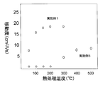
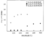
- FIG. It is a schematic sectional drawing of the field effect transistor of other embodiment of this invention. It is a schematic sectional drawing of the field effect transistor of other embodiment of this invention. It is a schematic sectional drawing of the field effect transistor of other embodiment of this invention. It is a schematic sectional drawing of the field effect transistor of other embodiment of this invention. It is a graph which shows the relationship between the heat processing temperature of a semiconductor layer, and a mobility. It is a graph which shows the relationship between the heat processing temperature of a semiconductor layer, and a mobility.
- a field effect transistor having high mobility and low S value can be obtained.
- a field effect transistor with high characteristics can be obtained even with a low-temperature or short-time thermal history (heat treatment).
- the mobility may be lowered, the S value may be increased, the moisture resistance may be lowered, or the chemical resistance to acid / alkali may be lowered. There is.
- the off current and the gate leakage current may be increased, the S value may be increased, the plasma resistance may be decreased, or the threshold may be negative and normally on.
- In / (In + Zn) is preferably 0.3 to 0.75, more preferably 0.35 to 0.7.
- In / (In + X) is preferably 0.45 to 0.98, more preferably 0.65 to 0.98, and particularly preferably 0.7 to 0.97.
- Zn / (X + Zn) is preferably 0.45 to 0.98, more preferably 0.6 to 0.98, and still more preferably 0.7 to 0.97.
- the semiconductor layer further satisfies the following ratio (4) (atomic ratio).
- ratio (4) (atomic ratio).
- X / (In + Zn + X) 0.01 to 0.2 (4) If the ratio of X is greater than 0.2, the S value may increase, the mobility may decrease, and the threshold voltage may increase. On the other hand, if it is less than 0.01, there is a risk that the thermal stability and heat resistance will decrease, the moisture resistance will decrease, the chemical resistance to acids, alkalis, etc. will decrease, and the threshold voltage shift will increase. is there.
- X / (In + Zn + X) is more preferably 0.02 to 0.15, and particularly preferably 0.03 to 0.1.
- the semiconductor layer satisfies the following ratio (5) or (6) (atomic ratio) depending on the application.
- ratio (5) 0.3 to 0.5
- In / (In + Zn + X) 0.5 to 0.7 (not including 0.5) (6)
- the ratio of (5) can easily reduce the off-current and increase the on-off ratio.
- the ratio is (6), the mobility can be increased and the threshold voltage can be decreased.
- the element X is preferably Zr or Hf, and particularly preferably Zr, because the thermal stability, heat resistance, and chemical resistance are improved and the S value and off-current can be reduced.
- the element X is preferably Zr, Hf, Ge, Si, or Ti.
- the element X is preferably Cu, Ni, Co, Fe, Cr, Mn, W, Mo, V, and Nb.
- the field effect transistor of the present invention contains an In (indium) element and a Zn (zinc) element and one or more elements X selected from the following group A in the atomic ratios of (1) to (3) below. It has a semiconductor layer made of a complex oxide.
- a field effect transistor having high mobility and low S value can be obtained.
- a field effect transistor with high characteristics can be obtained even with a low-temperature or short-time thermal history (heat treatment).
- the mobility may be lowered, the S value may be increased, the moisture resistance may be lowered, or the chemical resistance to acid / alkali may be lowered. There is.
- the off current and the gate leakage current may be increased, the S value may be increased, the plasma resistance may be decreased, or the threshold may be negative and normally on.
- In / (In + Zn) is preferably 0.3 to 0.75, more preferably 0.35 to 0.7.
- In / (In + X) is usually 0.29 to 0.99, preferably 0.59 to 0.98, more preferably 0.6 to 0.97, and further preferably 0.65 to 0.96. Particularly preferred is 0.7 to 0.95.
- Zn / (X + Zn) is preferably 0.45 to 0.98, more preferably 0.6 to 0.98, and even more preferably 0. 0.7 to 0.97, particularly preferably 0.75 to 0.90.
- the semiconductor layer further satisfies the following ratio (4) (atomic ratio).
- X / (In + Zn + X) 0.02 to 0.3 (4) If the ratio of X is greater than 0.3, the S value may increase, the mobility may decrease, and the threshold voltage may increase. On the other hand, if it is smaller than 0.02, the thermal stability and heat resistance are lowered, the moisture resistance is lowered, the chemical resistance to acids and alkalis is lowered, the off-current is increased, the threshold voltage is increased. There is a risk of a large shift.
- X / (In + Zn + X) is more preferably 0.04 to 0.25, further preferably 0.055 to 0.2, and particularly preferably 0.06 to 0.15.
- the semiconductor layer satisfy the following ratio (5) or (6) (atomic ratio) because it can be used properly depending on the application.
- ratio (5) 0.3 to 0.5
- In / (In + Zn + X) 0.5 to 0.7 (0.5 is not included) (6)
- the ratio (5) the off-current can be easily reduced and the on-off ratio can be increased.
- the ratio is (6), the mobility can be increased and the threshold voltage can be decreased.
- the element X is preferably Al or B. Also preferred is Sc or Y. Furthermore, lanthanoids (La, Ce, Pr, Nd, Sm, Eu, Gd, Tb, Dy, Ho, Er, Tm, Yb, Lu) are also preferable.
- the field effect transistor of the present invention is not particularly limited as long as it has the semiconductor layer shown in the first aspect or the second aspect described above.
- a known structure such as a top gate type or a bottom gate type can be used.
- a configuration example of a field effect transistor will be described with reference to the drawings.
- FIG. 1 is a schematic cross-sectional view of a field effect transistor according to an embodiment of the present invention.
- the field effect transistor 1 is a bottom gate type, and a gate electrode 12 is formed in a stripe shape on a silicon substrate 10 having a thermal oxide film 11.
- a gate insulating film 13 is provided so as to cover the gate electrode 12, and a semiconductor layer 14 (active layer) is formed on the gate insulating film 13 and on the gate electrode 12.
- a source electrode 15 is connected to one end 14 a of the semiconductor layer 14 in a direction orthogonal to the gate electrode 12. Further, the drain electrode 16 is connected to the other end 14 b facing the one end 14 a of the semiconductor layer 14.
- FIG. 2 is a schematic top view showing the positional relationship between the gate electrode 12, the semiconductor layer 14, the source electrode 15, and the drain electrode 16. Some members are omitted for visualization of the positional relationship.
- the semiconductor layer is preferably protected by a protective layer.
- a protective layer In the case of a bottom gate type transistor, if there is no protective layer, the main part of the semiconductor layer is exposed, so the effect of the protective layer is great.
- 3 and 4 are schematic cross-sectional views of a field effect transistor according to another embodiment of the present invention.
- the field effect transistors 2 and 3 have the same configuration as the field effect transistor 1 described above except that the protective layer 17 is formed.
- FIG. 5 is a schematic cross-sectional view illustrating an example of a top gate type field effect transistor.
- a source electrode 35 and a drain electrode 36 are formed on a substrate 30, and a semiconductor layer 34 is provided so as to cover the gap and part of these electrodes.
- a gate electrode 32 is formed on the semiconductor layer 34 via a gate insulating film 33.
- the substrate 30 serves as the protective layer 37.
- Substrate there is no particular limitation, and those known in this technical field can be used.
- glass substrates such as alkali silicate glass, non-alkali glass and quartz glass, silicon substrates, resin substrates such as acrylic, polycarbonate and polyethylene naphthalate (PEN), polymer film bases such as polyethylene terephthalate (PET) and polyamide Materials can be used.
- the thickness of the substrate or base material is generally 0.1 to 10 mm, preferably 0.3 to 5 mm.
- a glass substrate those chemically or thermally reinforced are preferred.
- a glass substrate and a resin substrate are preferable, and a glass substrate is particularly preferable.
- weight reduction is required, a resin substrate or a polymer material is preferable.
- the semiconductor layer contains In (indium), Zn (zinc) and the element X shown in the first aspect or the second aspect described above in a ratio of (1) to (3), preferably (1) to It consists of the complex oxide contained so that the ratio of (4) may be satisfy
- Such a semiconductor layer can be produced, for example, by forming a thin film using the complex oxide target (target for semiconductor layer) of the present invention.
- the target for a semiconductor layer of the present invention is composed of a composite oxide sintered body satisfying the ratios (1) to (3) or (1) to (4) shown in the first aspect or the second aspect.
- the target is made of, for example, a mixed powder containing indium oxide, zinc oxide, and an oxide of element X so as to satisfy the above element ratio.
- the raw material powder can be produced by finely pulverizing with a ball mill or the like, then forming into a target and firing.
- a part of raw material powder to be used may be one obtained by collecting from high-purity indium oxide-containing scrap such as target scraps and used targets.
- indium oxide recovered from the ITO target preferably contains Sn (tin) as an impurity.
- Indium oxide can be recovered by a known method such as the method described in JP-A No. 2002-069544.
- the element X shown in the first aspect is Zr, Hf, Ge, Si, Ti, V, and Nb, it is easy to manufacture a target having a particularly good appearance and high bending strength.
- the purity of each raw material powder is usually 99.9% (3N) or higher, preferably 99.99% (4N) or higher, more preferably 99.995% or higher, particularly preferably 99.999% (5N) or higher. . If the purity of each raw material powder is less than 99.9% (3N), the semiconductor characteristics may be deteriorated due to impurities, appearance defects such as uneven color and spots may occur, and reliability may be reduced. is there.
- the specific surface area of the indium oxide powder is 8 to 10 m 2 / g
- the specific surface area of the zinc oxide powder is 2 to 4 m 2 / g
- the specific surface area of the oxide of the element X is 5 to 10 m 2 / g (more preferably Is preferably 8 to 10 m 2 / g).
- the median diameter of the indium oxide powder is preferably 0.2 to 2 ⁇ m
- the median diameter of the zinc oxide powder is preferably 0.8 to 1.6 ⁇ m.
- the difference in specific surface area is preferably 5 m 2 / g or less. If the specific surface area is too different, efficient pulverization and mixing cannot be performed, and oxide particles of the element X may remain in the sintered body.
- the mixed powder is mixed and ground using, for example, a wet medium stirring mill.
- the specific surface area after pulverization is increased by 1.5 to 2.5 m 2 / g from the specific surface area of the raw material mixed powder, or is pulverized so that the average median diameter after pulverization is 0.6 to 1 ⁇ m. It is preferable to do.
- a high-density oxide sintered body can be obtained without requiring a calcination step at all. Moreover, a reduction process is also unnecessary.
- the increase in the specific surface area of the raw material mixed powder is less than 1.0 m 2 / g or the average median diameter of the raw material mixed powder after pulverization exceeds 1 ⁇ m, the sintered density may not be sufficiently increased.
- the increase in the specific surface area of the raw material mixed powder exceeds 3.0 m 2 / g, or if the average median diameter after pulverization is less than 0.6 ⁇ m, contamination from the pulverizer during pulverization (impurity contamination amount) ) May increase.
- the specific surface area of each powder is a value measured by the BET method.
- the median diameter of the particle size distribution of each powder is a value measured with a particle size distribution meter.
- These values can be adjusted by pulverizing the powder by a dry pulverization method, a wet pulverization method or the like.
- the raw material after the pulverization step is dried with a spray dryer or the like and then molded.
- a known method such as pressure forming or cold isostatic pressing can be employed.
- the obtained molded product is sintered to obtain a sintered body.
- Sintering is preferably performed at 1350 to 1600 ° C. for 2 to 20 hours. When the temperature is lower than 1350 ° C., the density is not improved. When the temperature exceeds 1600 ° C., zinc is evaporated, the composition of the sintered body is changed, or voids (voids) are generated in the sintered body due to the evaporation. There is. Sintering is preferably performed in an oxygen atmosphere by circulating oxygen or under pressure. Thereby, transpiration of zinc can be suppressed, and a sintered body free from voids (voids) can be obtained. Since the sintered body manufactured in this manner has a high density and generates less nodules and particles during use, an oxide semiconductor film having excellent film characteristics can be manufactured.
- the oxide sintered body becomes a target by performing processing such as polishing.
- the sintered body is ground by, for example, a surface grinder so that the surface roughness Ra is 5 ⁇ m or less.
- the sputter surface of the target may be mirror-finished so that the average surface roughness Ra is 1000 angstroms or less.
- a known polishing technique such as mechanical polishing, chemical polishing, mechanochemical polishing (a combination of mechanical polishing and chemical polishing) can be used.
- polishing to # 2000 or more with a fixed abrasive polisher polishing liquid: water
- lapping with loose abrasive lapping abrasive: SiC paste, etc.
- lapping by changing the abrasive to diamond paste can be obtained by:
- Such a polishing method is not particularly limited.
- the film forming method include a sputtering method, a PLD (pulse laser deposition) method, a vacuum deposition method, and an ion plating method.
- cleaning, etc. can be used for the cleaning process of a target.
- cleaning, etc. can be used for the cleaning process of a target.
- ultrasonic cleaning and the like can also be performed.
- a method of performing multiple oscillation at a frequency of 25 to 300 KHz is effective.
- the particle size of each compound in the oxide sintered body is preferably 20 ⁇ m or less, more preferably 10 ⁇ m or less, and particularly preferably 5 ⁇ m or less.
- the particle size is an average particle size measured with an electron probe microanalyzer (EPMA).
- the crystal grain size is, for example, the raw material indium oxide, the oxide of X element, the blending ratio of each powder of zinc oxide, the grain size of the raw material powder, the purity, the temperature rise time, the sintering temperature, the sintering time, It is obtained by adjusting the sintering atmosphere and the temperature lowering time. If the particle size of the compound is larger than 20 ⁇ m, nodules may be generated during sputtering.
- the density of the target is preferably 95% or more of the theoretical density, more preferably 98% or more, and particularly preferably 99% or more. If the density of the target is less than 95%, the strength is insufficient and the target may be damaged during film formation. In addition, performance may be uneven when a transistor is manufactured.
- the theoretical relative density of the target is the specific gravity of each oxide (for example, ZnO is 5.66 g / cm 3 , In 2 O 3 is 7.12 g / cm 3 , and ZrO 2 is 5.98 g / cm 3 ). The density is calculated from the quantitative ratio, and the ratio with the density measured by the Archimedes method is calculated to obtain the theoretical relative density.
- the target bulk resistance is preferably 20 m ⁇ or less, more preferably 10 m ⁇ or less, further preferably 5 m ⁇ or less, and particularly preferably 2 m ⁇ cm or less. . If it is greater than 20 m ⁇ , the target may be damaged during film formation by DC sputtering. In addition, a spark may be generated due to abnormal discharge, and the target may be cracked, or particles ejected by the spark may adhere to the deposition substrate and deteriorate the performance as an oxide semiconductor film. In addition, the target may break during discharge.
- the bulk resistance is a value measured by a four-probe method using a resistivity meter.
- the bending strength of the target of the present invention is preferably 8 kg / mm 2 or more, more preferably 10 kg / mm 2 or more, and particularly preferably 12 kg / mm 2 or more.
- the target is required to have a certain level of bending force because a load is applied during transportation and mounting of the target, and the target may be damaged. If the target is less than 8 kg / mm 2 , it cannot be used as a target. There is a fear.
- the bending strength of the target can be measured according to JIS R 1601.
- the target relating to the second aspect of the present invention is further selected from the group consisting of Sn (tin), Ge (germanium), Si (silicon), Ti (titanium), Zr (zirconium) and Hf (hafnium). It is preferable to contain 100 to 10,000 ppm of one or more elements. When these elements are included, the target density is improved, the strength is increased, the resistance is decreased, the color unevenness is decreased, the uniformity is improved, the abnormal discharge and the yellow flakes are decreased, and the quality as a semiconductor target is improved. It can be expected to improve.
- the above elements may be contained as impurities using raw materials recovered from a sintered body (target) containing these elements. Moreover, you may add to a raw material as a metal powder or an oxide.
- the semiconductor layer is preferably an amorphous film.
- an amorphous film By being an amorphous film, adhesion to an insulating film and a protective layer is improved, and uniform transistor characteristics can be easily obtained even in a large area.
- whether the semiconductor layer is an amorphous film can be confirmed by X-ray crystal structure analysis. The case where no clear peak is observed is amorphous.
- the electron carrier concentration of the semiconductor layer is preferably 10 13 to 10 18 / cm 3 , particularly preferably 10 14 to 10 17 / cm 3 .
- the band gap is preferably 2.0 to 6.0 eV, and more preferably 2.8 to 5.0 eV. If the band gap is smaller than 2.0 eV, visible light is absorbed and the field effect transistor may malfunction. On the other hand, if it is larger than 6.0 eV, it is difficult to supply carriers and the field effect transistor may not function.
- the semiconductor layer is preferably a non-degenerate semiconductor exhibiting a thermal activation type. If the semiconductor is a degenerate semiconductor, there are too many carriers, which may increase the off-current / gate leakage current, or the threshold value may become negative, resulting in normally-on. Whether the semiconductor layer is a non-degenerate semiconductor can be determined by measuring temperature changes in mobility and carrier density using the Hall effect. In addition, the semiconductor layer can be a non-degenerate semiconductor by adjusting the oxygen partial pressure during film formation or by performing post-processing to control the amount of oxygen defects and optimize the carrier density.
- the surface roughness (RMS) of the semiconductor layer is preferably 1 nm or less, more preferably 0.6 nm or less, and particularly preferably 0.3 nm or less. If it is larger than 1 nm, the mobility may decrease.
- the semiconductor layer is preferably an amorphous film that maintains at least part of the edge sharing structure of the bixbite structure of indium oxide. Whether or not the amorphous film containing indium oxide maintains at least a part of the edge sharing structure of the bixbite structure of indium oxide is determined by small angle incident X-ray scattering (GIXS) using high-intensity synchrotron radiation or the like. From the radial distribution function (RDF) obtained by the above, it can be confirmed that the peak representing In—X (X is In, Zn) is between 0.30 and 0.36 nm. For details, the following documents may be referred to. F. Utsuno, et al. , Thin Solid Films, Volume 496, 2006, Pages 95-98
- a / B> 0.7 is preferably satisfied, A / B> 0.85 is more preferable, A / B> 1 is further more preferable, and A / B> 1.2 is particularly preferable.
- a / B is 0.7 or less, when a semiconductor layer is used as an active layer of a transistor, there is a possibility that the mobility may decrease or the threshold value or S value may become too large. It is considered that the small A / B reflects the poor short-range order of the amorphous film.
- the average In—In bond distance is preferably 0.3 to 0.322 nm, particularly preferably 0.31 to 0.32 nm.
- the average bond distance of In—In can be determined by X-ray absorption spectroscopy.
- the measurement by X-ray absorption spectroscopy shows an X-ray absorption wide-area microstructure (EXAFS) that has spread to a high energy as high as several hundred eV from the rise.
- EXAFS is caused by backscattering of electrons by atoms around the excited atom. Interference effect between the flying electron wave and the back-scattered wave occurs. Interference depends on the wavelength of the electronic state and the optical path length to and from surrounding atoms.
- a radial distribution function (RDF) is obtained by Fourier transforming EXAFS.
- the average bond distance can be estimated from the RDF peak.
- the film thickness of the semiconductor layer is usually 0.5 to 500 nm, preferably 1 to 150 nm, more preferably 3 to 80 nm, and particularly preferably 10 to 60 nm. If it is thinner than 0.5 nm, it is difficult to form a uniform film industrially. On the other hand, if it is thicker than 500 nm, the film formation time becomes long and cannot be adopted industrially. When the thickness is in the range of 3 to 80 nm, TFT characteristics such as mobility and on / off ratio are particularly good.
- the semiconductor layer is preferably an amorphous film, and the energy width (E 0 ) of the delocalized level is preferably 14 meV or less.
- the energy width (E 0 ) of the delocalized level of the semiconductor layer is more preferably 10 meV or less, further preferably 8 meV or less, and particularly preferably 6 meV or less.
- the energy width (E 0 ) of the delocalized level is larger than 14 meV, when the semiconductor layer is used as the active layer of the transistor, the mobility may be lowered or the threshold value or the S value may be too large. It is considered that the large energy width (E 0 ) of the delocalized level of the semiconductor layer reflects the poor short-range order of the amorphous film.
- the field effect transistor preferably has a protective layer of semiconductor. Without the semiconductor protective layer, oxygen in the surface layer of the semiconductor is desorbed in a vacuum or under a low pressure, which may increase the off-current or make the threshold voltage negative. Further, even in the atmosphere, there is a risk that variations in transistor characteristics such as threshold voltage may increase due to the influence of surroundings such as humidity.
- the material for forming the semiconductor protective layer is not particularly limited. What is generally used can be arbitrarily selected as long as the effects of the present invention are not lost.
- SiO 2, SiNx, Al 2 O 3, Ta 2 O 5, TiO 2, MgO, ZrO 2, CeO 2, K 2 O, Li 2 O, Na 2 O, Rb 2 O, Sc 2 O 3, Y 2 O 3 , Hf 2 O 3 , CaHfO 3 , PbTi 3 , BaTa 2 O 6 , SrTiO 3 , AlN, or the like can be used.
- the number of oxygen in these oxides does not necessarily match the stoichiometric ratio (for example, it may be SiO 2 or SiO x).
- SiNx may contain a hydrogen element.
- Such a protective film may have a structure in which two or more different insulating films are stacked.
- the protective layer may be crystalline, polycrystalline, or amorphous, but is preferably polycrystalline or amorphous that is easy to produce industrially. However, it is particularly preferred that the protective layer is amorphous. If it is not an amorphous film, the smoothness of the interface is poor, and the mobility may be lowered, or the threshold voltage and S value may be too large.
- the protective layer of the semiconductor layer is preferably an amorphous oxide or an amorphous nitride, and particularly preferably an amorphous oxide. Further, if the protective layer is not an oxide, oxygen in the semiconductor moves to the protective layer side, and there is a possibility that the off current becomes high or the threshold voltage becomes negative and normally off. Further, an organic insulating film such as poly (4-vinylphenol) (PVP) or parylene may be used for the protective layer of the semiconductor layer. Further, the protective layer of the semiconductor layer may have a laminated structure of two or more layers of an inorganic insulating film and an organic insulating film.
- Gate insulating film There is no particular limitation on the material for forming the gate insulating film. What is generally used can be arbitrarily selected as long as the effects of the invention of the present embodiment are not lost. For example, SiO 2, SiNx, Al 2 O 3, Ta 2 O 5, TiO 2, MgO, ZrO 2, CeO 2, K 2 O, Li 2 O, Na 2 O, Rb 2 O, Sc 2 O 3, Y 2 O 3 , Hf 2 O 3 , CaHfO 3 , PbTi 3 , BaTa 2 O 6 , SrTiO 3 , AlN, or the like can be used.
- the number of oxygen in these oxides does not necessarily match the stoichiometric ratio (for example, it may be SiO 2 or SiO x).
- SiNx may contain a hydrogen element.
- Such a gate insulating film may have a structure in which two or more different insulating films are stacked.
- the gate insulating film may be crystalline, polycrystalline, or amorphous, but is preferably polycrystalline or amorphous that is easy to manufacture industrially.
- the gate insulating film may be an organic insulating film such as poly (4-vinylphenol) (PVP) or parylene. Further, the gate insulating film may have a stacked structure of two or more layers of an inorganic insulating film and an organic insulating film.
- Electrode There are no particular limitations on the material for forming each of the gate electrode, the source electrode, and the drain electrode, and any material generally used can be selected as long as the effects of the present invention are not lost.
- transparent electrodes such as indium tin oxide (ITO), indium zinc oxide, ZnO, SnO 2 , metal electrodes such as Al, Ag, Cr, Ni, Mo, Au, Ti, Ta, Cu, or these An alloy metal electrode can be used.
- ITO indium tin oxide
- ZnO zinc oxide
- SnO 2 zinc oxide
- metal electrodes such as Al, Ag, Cr, Ni, Mo, Au, Ti, Ta, Cu, or these
- the resistance of the interface with the semiconductor electrode may be adjusted by plasma treatment, ozone treatment or the like.
- the manufacturing method of the present invention includes a step of forming a semiconductor layer by DC or AC sputtering using the above-described target of the present invention, and a step of heat-treating at 70 to 350 ° C. after forming the semiconductor layer, To do.
- Each constituent member (layer) of the above-described field effect transistor can be formed by a method known in this technical field. Specifically, as a film formation method, a chemical film formation method such as a spray method, a dip method, or a CVD method, or a physical film formation method such as a sputtering method, a vacuum evaporation method, an ion plating method, or a pulse laser deposition method. The method can be used. Since the carrier density is easily controlled and the film quality can be easily improved, a physical film formation method is preferably used, and a sputtering method is more preferably used because of high productivity.
- a method using a sintered complex oxide target In sputtering, a method using a sintered complex oxide target, a method using co-sputtering using a plurality of sintered targets, a method using reactive sputtering using an alloy target, and the like can be used.
- the uniformity and reproducibility are deteriorated, or the energy width of delocalized levels (E 0 ) May increase, and the transistor characteristics may be deteriorated, for example, the mobility may be decreased or the threshold voltage may be increased.
- a composite oxide sintered target is used.
- the formed film can be patterned by various etching methods.
- the semiconductor layer is formed by DC or AC sputtering using the target of the present invention.
- DC or AC sputtering damage during film formation can be reduced as compared with RF sputtering. For this reason, in the field effect transistor, effects such as a reduction in threshold voltage shift, an improvement in mobility, a reduction in threshold voltage, and a reduction in S value can be expected.
- heat treatment is performed at 70 to 350 ° C. If it is lower than 70 ° C., the thermal stability and heat resistance of the obtained transistor may be lowered, the mobility may be lowered, the S value may be increased, or the threshold voltage may be increased. On the other hand, when the temperature is higher than 350 ° C., a substrate having no heat resistance may not be used, the cost of heat treatment equipment may be increased, the interface of the protective layer, the insulating film, or the semiconductor layer may be deteriorated, or the moisture pressure may be lowered. When the film is formed, it may crystallize and an amorphous film may not be obtained.
- the heat treatment temperature is preferably 80 to 260 ° C, more preferably 90 to 180 ° C, and further preferably 100 to 150 ° C.
- a heat treatment temperature of 180 ° C. or lower is preferable because a resin substrate having low heat resistance such as PEN can be used as the substrate.
- the heat treatment time is usually preferably 1 second to 24 hours, but is preferably adjusted according to the treatment temperature. For example, at 70 to 180 ° C., 10 minutes to 24 hours are more preferable, 20 minutes to 6 hours are more preferable, and 30 minutes to 3 hours are particularly preferable. At 180 to 260 ° C., 6 minutes to 4 hours is more preferable, and 15 minutes to 2 hours is more preferable. At 260 to 300 ° C., 30 seconds to 4 hours is more preferable, and 1 minute to 2 hours is particularly preferable. At 300 to 350 ° C., 1 second to 1 hour is more preferable, and 2 seconds to 30 minutes is particularly preferable.
- the heat treatment is preferably performed in an inert gas in an environment where the oxygen partial pressure is 10 ⁇ 3 Pa or less, or after the semiconductor layer is covered with a protective layer. Reproducibility is improved under the above conditions.
- the inert gas N 2 , He, Ne, Ar, Kr, and Xe are preferable.
- the field effect transistor of the present invention mobility is preferably at least 1 cm 2 / Vs, more preferably at least 3 cm 2 / Vs, particularly preferably at least 8 cm 2 / Vs. If it is smaller than 1 cm 2 / Vs, the switching speed becomes slow, and there is a possibility that it cannot be used for a large-screen high-definition display.
- the on / off ratio is preferably 10 6 or more, more preferably 10 7 or more, and particularly preferably 10 8 or more.
- the off current is preferably 2 pA or less, more preferably 1 pA or less, further preferably 0.5 pA or less, and particularly preferably 0.2 pA or less.
- the gate leakage current is preferably 1 pA or less. If it is larger than 1 pA, the contrast may deteriorate when used as a TFT of a display.
- the threshold voltage is usually 0 to 10V, preferably 0 to 4V, more preferably 0 to 3V, and particularly preferably 0 to 2V. If it is less than 0V, it is normally on, and it is necessary to apply a voltage when it is off, which may increase power consumption. If it is greater than 10V, the drive voltage may increase and the power consumption may increase, or high mobility may be required.
- the S value is preferably 0.8 V / dec or less, more preferably 0.3 V / dec or less, further preferably 0.25 V / dec or less, and particularly preferably 0.2 V / dec or less. If it is greater than 0.8 V / dec, the drive voltage may increase and power consumption may increase. In particular, when used in an organic EL display, it is preferable to set the S value to 0.3 V / dec or less because of direct current drive because power consumption can be greatly reduced.
- the S value is a value indicating the steepness of the drain current that rises sharply from the off state to the on state when the gate voltage is increased from the off state.
- S value dVg / dlog (Ids)
- the smaller the S value, the sharper the rise (All about Thin Film Transistor Technology", Ikuhiro Ukai, 2007, Industrial Research Committee).
- the S value is large, it is necessary to apply a high gate voltage when switching from on to off, and power consumption may increase.
- the shift amount of the threshold voltage before and after being applied for 100 hours at a DC voltage of 10 ⁇ A at 50 ° C. is preferably 1.0 V or less, and more preferably 0.5 V or less. If it is greater than 1V, the image quality may change when used as a transistor in an organic EL display.
- the hysteresis when the gate voltage is raised and lowered by the transfer curve is small.
- the ratio W / L of the channel width W to the channel length L is usually 0.1 to 100, preferably 0.5 to 20, and particularly preferably 1 to 8. If W / L exceeds 100, the leakage current may increase or the on-off ratio may decrease. If it is less than 0.1, the field effect mobility may be lowered, or pinch-off may be unclear.
- the channel length L is usually 0.1 to 1000 ⁇ m, preferably 1 to 100 ⁇ m, more preferably 2 to 10 ⁇ m. If the thickness is 0.1 ⁇ m or less, it is difficult to produce industrially and the leakage current may be increased. If the thickness is 1000 ⁇ m or more, the device becomes too large, which is not preferable.
- the field effect transistor of the present invention preferably has a structure for shielding the semiconductor layer. If the semiconductor layer does not have a structure that shields light (for example, a light shielding layer), when electrons enter the semiconductor layer, carrier electrons may be excited and off current may be increased.
- the light shielding layer is preferably a thin film having absorption at 300 to 800 nm.
- the light shielding layer may be either the upper part or the lower part of the semiconductor layer, but is preferably on both the upper part and the lower part. Further, the light shielding layer may also be used as a gate insulating film, a black matrix, or the like. When the light shielding layer is on only one side, it is necessary to devise a structure so that light is not irradiated to the semiconductor layer from the side where the light shielding layer is not present.
- the contact layer it is preferable to provide a contact layer between the semiconductor layer and the source or drain electrode.
- a material for forming the contact layer a composite oxide having the same composition as that of the semiconductor layer described above can be used. That is, the contact layer is preferably an oxide whose main component is an element contained in the semiconductor layer, such as In or Zn. If these elements are not included, element movement occurs between the contact layer and the semiconductor layer, and the threshold voltage may shift significantly when a stress test or the like is performed.
- a contact layer having the same composition ratio as the semiconductor layer can be formed by changing the film formation conditions, a layer having a composition ratio different from that of the semiconductor layer can be formed, or a semiconductor electrode
- the contact portion may be formed by increasing the resistance by plasma treatment or ozone treatment, or a layer having a higher resistance may be formed by film formation conditions such as oxygen partial pressure when forming the semiconductor layer.
- an oxide resistance layer having higher resistance than the semiconductor layer is provided between the semiconductor layer and the gate insulating film and / or between the semiconductor layer and the protective layer. . If the oxide resistance layer is not provided, off current may be generated, or the threshold voltage may be negative and normally on. Further, the semiconductor layer may be altered during the post-treatment process such as protective film formation or etching, and the characteristics may be deteriorated.
- the following can be illustrated as an oxide resistance layer.
- ⁇ Amorphous oxide film with the same composition as the semiconductor layer deposited at a higher oxygen partial pressure than when the semiconductor film was deposited ⁇ Amorphous oxide film with the same composition as the semiconductor layer but with a different composition ratio
- An amorphous oxide film containing In and Zn and containing an element X different from the semiconductor layer a polycrystalline oxide film containing indium oxide as a main component.
- Indium oxide as a main component Zn, Cu, Co, Ni, Mn
- the composition contained in the polycrystalline oxide film / semiconductor layer doped with one or more positive divalent elements such as Mg is further selected from Cu, Co, Ni, Mn, Fe, Mg, Ca, Sr, Ba, Ag, Au Amorphous oxide film with one or more elements added
- the In composition ratio is the semiconductor layer. Is preferably less. Moreover, it is preferable that the composition ratio of the element X is larger than that of the semiconductor layer.
- the oxide resistance layer is preferably an oxide containing each element of In and Zn. If these elements are not included, element movement occurs between the oxide resistance layer and the semiconductor layer, and the threshold voltage may shift significantly when a stress test or the like is performed.
- an amorphous oxide film in which one or more elements selected from Cu, Co, Ni, Mn, Fe, Mg, Ca, Sr, Ba, Ag, Au are added to the composition contained in the semiconductor layer
- the In composition ratio is preferably smaller than that of the semiconductor layer.
- Example 1 Production of sputtering target As raw materials, powders of indium oxide, zinc oxide and zirconium oxide have an atomic ratio [In / (In + Zn + Zr)] of 0.48 and an atomic ratio [Zn / (In + Zn + Zr)] of 0.50. Mixing was performed so that the atomic ratio [Zr / (In + Zn + Zr)] was 0.02. This was supplied to a wet ball mill and mixed and ground for 72 hours to obtain a raw material fine powder. After granulating the obtained raw material fine powder, it was press-molded to a size of 10 cm in diameter and 5 mm in thickness, put in a firing furnace and fired at 1500 ° C.
- the target had a bulk resistance of 3 m ⁇ and a theoretical relative density of 0.99.
- the theoretical relative density was obtained by calculating the ratio of the density calculated from the specific gravity of each oxide and the amount ratio thereof to the density measured by the Archimedes method.
- the target manufactured in (1) is mounted on a DC magnetron sputtering film forming apparatus, which is one of the DC sputtering methods, formed on the gate insulating film, and then patterned to form a semiconductor layer (film thickness). 50 nm).
- Sputtering conditions are: substrate temperature: 25 ° C., ultimate pressure: 1 ⁇ 10 ⁇ 6 Pa, atmospheric gas: Ar 99.5% and oxygen 0.5%, sputtering pressure (total pressure): 2 ⁇ 10 ⁇ 1 Pa, input power The distance was 100 W, the film formation time was 6 minutes, and the ST distance was 110 mm.
- a source / drain electrode made of In 2 O 3 —ZnO was formed using a lift-off process and RF magnetron sputtering (room temperature, Ar 100%). Thereafter, a field effect transistor was manufactured by heat treatment at 170 ° C. for 2 hours in a nitrogen environment (a bottom-gate field effect transistor having W of 40 ⁇ m and L of 4 ⁇ m in FIG. 2).
- a semiconductor layer was formed on the glass substrate (Corning 1737) using the target manufactured in Example (1) and evaluated.
- the semiconductor layer was formed in the same manner as in Example (2) using a DC magnetron sputtering film forming apparatus. As a result, an oxide thin film having a thickness of 50 nm was formed on the glass substrate.
- the atomic ratio [In / (In + Zn + Zr)] was 0.49
- the atomic ratio [Zn / (In + Zn + Zr)] was 0.49
- the atomic ratio [Ga / (In + Zn + Zr)] was 0.02.
- the semiconductor film was heat-treated at 170 ° C. for 2 hours in a nitrogen environment.
- the carrier concentration and hole mobility of the semiconductor film after the heat treatment were measured with a hole measuring device.
- the result was n-type, the carrier concentration was 4 ⁇ 10 17 cm ⁇ 3 , and the hole mobility was 2 cm 2 / Vs.
- the Hall measuring device and the measurement conditions were as follows: ⁇ Hall measuring device manufactured by Toyo Technica: Resi Test 8310 ⁇ Measurement conditions Measurement temperature: Room temperature (25 °C) Measurement magnetic field: 0.5T Measurement current: 10 ⁇ 12 to 10 ⁇ 4 A Measurement mode: AC magnetic field hall measurement
- the surface roughness measured by AMF was RMS 0.2 nm.
- the band gap obtained optically was 3.8 eV.
- the Hall effect was measured by changing the measurement temperature in the range of 77 to 300K, it was confirmed that the semiconductor film was a non-degenerate semiconductor.
- the energy width (E 0 ) of the delocalized level was 6 meV or less from the relationship between the carrier concentration and the activation energy measured using the Hall effect while changing the temperature.
- a radial distribution function (RDF) obtained by X-ray scattering measurement confirmed that a peak representing In—In was observed at around 0.35 nm, and a ridge sharing structure of the bixbite structure of indium oxide remained. did it.
- a / B where A is the maximum value of RDF with an interatomic distance of 0.30 to 0.36 nm, and B is the maximum value of RDF with an interatomic distance of 0.36 to 0.42.
- the average In—In bond distance determined by X-ray absorption spectroscopy was 0.318 nm.
- Acid resistance and moisture resistance were evaluated as follows.
- the resistance before and after the test was measured and classified as follows.
- the rate of change was defined as the resistance value before the test divided by the resistance value after the test or the resistance value after the test divided by the resistance value before the test.
- ⁇ Change rate less than 2 times
- ⁇ Change rate 2 to 5 times change
- ⁇ Change rate 5 to 100 times change
- Table 1 shows the measurement results.
- Example 2 Comparative Examples 1 to 7
- a sputtering target was manufactured in the same manner as in Example 1 (1) except that the mixing ratio of the raw materials, indium oxide, zinc oxide, and X element oxide was adjusted to the composition shown in Table 1-4.
- a field effect transistor was fabricated and evaluated in the same manner as in Example 1 (2) except that the above sputtering target was used and the film formation conditions were changed as shown in Table 1-4.
- the raw materials used in place of zirconium oxide when manufacturing the sputtering target are as follows.
- Example 12 HfO 2 , manufactured by Kojundo Chemical Laboratory Co., Ltd., HFO01PB
- Example 13 GeO 2 , GEO06PB manufactured by Kojundo Chemical Laboratory Co., Ltd.
- Example 14 SiO 2 , manufactured by Kojundo Chemical Laboratory Co., Ltd., SIO12PB
- Example 15 TiO 2 , manufactured by Kojundo Chemical Laboratory Co., Ltd., TIO14PB
- Example 16 MnO 2 , manufactured by Kojundo Chemical Laboratory Co., Ltd., MNO03PB
- Example 17 WO 3, Kojundo Chemical Laboratory Co., Ltd.
- Example 18 MoO 3 , manufactured by Kojundo Chemical Laboratory Co., Ltd., MOO03PB
- Example 19 V 2 O 5 , manufactured by Kojundo Chemical Laboratory Co., Ltd., VVO09PB
- Example 20 Nb 2 O 5 , manufactured by Kojundo Chemical Laboratory Co., Ltd., NBO08PB
- Example 25 CuO, manufactured by Kojundo Chemical Laboratory Co., Ltd., CUO08PB
- Example 26 NiO, manufactured by Kojundo Chemical Laboratory Co., Ltd., NIO11PB
- Example 27 CoO, manufactured by Kojundo Chemical Laboratory Co., Ltd., COO03PB
- Example 28 FeO, manufactured by Kojundo Chemical Laboratory Co., Ltd., FEO01PB
- Example 29 Cr 2 O 3 , manufactured by Kojundo Chemical Laboratory Co., Ltd., CRO01GB
- Example 21 after forming the source / drain electrodes, a protective layer was formed by forming 300 nm of SiO 2 by RF magnetron sputtering to produce the field effect transistor shown in FIG.
- Example 22 and Comparative Examples 1 to 7 the semiconductor layer was formed by RF sputtering.
- the target was mounted on an RF magnetron sputtering film forming apparatus to form a film.
- the sputtering conditions here are: substrate temperature: 25 ° C., ultimate pressure: 1 ⁇ 10 ⁇ 6 Pa, atmospheric gas: Ar 99.5% and oxygen 0.5%, sputtering pressure (total pressure); 2 ⁇ 10 ⁇ 1 Pa
- the input power was 100 W
- the film formation time was 8 minutes
- the ST distance was 100 mm.
- Example 23 a silicon substrate with a SiO 2 thermal oxide film was used. The thickness of the SiO 2 thermal oxide film was 100 nm.
- the gate insulating film is a SiO 2 thermal oxide film, and the silicon substrate serves as a gate electrode and a substrate.
- a semiconductor layer, a source electrode, and a drain electrode were formed in the same manner as in Example 1 on a silicon substrate with a SiO 2 thermal oxide film.
- Example 30 As raw materials, powders of indium oxide, zinc oxide and zirconium oxide have an atomic ratio [In / (In + Zn + Zr)] of 0.4, an atomic ratio [Zn / (In + Zn + Zr)] of 0.4, and an atomic ratio [Zr / (In + Zn + Zr). )] was 0.2. This was supplied to a wet ball mill and mixed and ground for 72 hours to obtain a raw material fine powder. After granulating the obtained raw material fine powder, it was press-molded to a size of 20 cm in diameter and 5 mm in thickness, and then placed in a firing furnace and fired at 1400 ° C.
- the target had a bulk resistance of 5 m ⁇ and a theoretical relative density of 0.98.
- the target bending strength was 12 kg / mm 2 .
- a target having no color unevenness and high appearance uniformity was obtained.
- Comparative Example 8 As raw materials, powders of indium oxide, zinc oxide and gallium oxide have an atomic ratio [In / (In + Zn + Ga)] of 0.4, an atomic ratio [Zn / (In + Zn + Ga)] of 0.4, and an atomic ratio [Ga / (In + Zn + Ga). )] was 0.2. This was supplied to a wet ball mill and mixed and ground for 72 hours to obtain a raw material fine powder. After granulating the obtained raw material fine powder, it was press-molded to a size of 20 cm in diameter and 5 mm in thickness, and then placed in a firing furnace and fired at 1400 ° C. for 12 hours to obtain a sintered body (target). It was. The target had a bulk resistance of 70 m ⁇ and a theoretical relative density of 0.82. The target bending strength was 7 kg / mm 2 . In addition, slight uneven color was confirmed on the target.
- FIG. 6 shows the relationship between the heat treatment temperature and the mobility of the semiconductor layer having the same composition as in Examples 1 and 5.
- the processing time is 2 hours.
- the mobility was stabilized by treatment at 150 ° C., whereas in the composition of Example 5, a treatment temperature of 300 ° C. or more was required to stabilize the mobility.
- Example 31 [Second embodiment] [Production of sputtering target]
- Example 31 (Target I)
- 5N purity 99.999%) indium oxide (INO04PB manufactured by Kojundo Chemical Laboratory Co., Ltd.), 5N zinc oxide (ZNO04PB manufactured by Kojundo Chemical Laboratory Co., Ltd.) and 5N aluminum oxide (stock) Company high purity chemical research laboratory company) powder
- atomic ratio [In / (In + Zn + Al)] is 0.48
- atomic ratio [Zn / (In + Zn + Al)] is 0.50
- atomic ratio [Al / (In + Zn + Al)] was mixed to 0.02. This was supplied to a wet ball mill and mixed and ground for 72 hours to obtain a raw material fine powder.
- the target After granulating the obtained raw material fine powder, it is press-molded to a size of 10 cm in diameter and 5 mm in thickness, put in a firing furnace and fired at 1500 ° C. for 12 hours to obtain a sintered body (target). It was.
- impurities such as Sn (tin), Ge (germanium), Si (silicon), Ti (titanium), Zr (zirconium), and Hf (hafnium) were not contained. Further, the target had a bulk resistance of 20 m ⁇ and a theoretical relative density of 0.95.
- Example 32 Powders of indium oxide, 5N zinc oxide (ZNO04PB manufactured by Kojundo Chemical Laboratory Co., Ltd.) and 4N aluminum oxide (ALO12PB manufactured by Kojundo Chemical Laboratory Co., Ltd.) recovered from used ITO targets as raw materials Were mixed so that the atomic ratio [In / (In + Zn + Al)] was 0.48, the atomic ratio [Zn / (In + Zn + Al)] was 0.50, and the atomic ratio [Al / (In + Zn + Al)] was 0.02. This was supplied to a wet ball mill and mixed and ground for 72 hours to obtain a raw material fine powder.
- the obtained raw material fine powder After granulating the obtained raw material fine powder, it is press-molded to a size of 10 cm in diameter and 5 mm in thickness, put in a firing furnace and fired at 1500 ° C. for 12 hours to obtain a sintered body (target). It was.
- the target When the target was pulverized and analyzed by ICP, 500 ppm of Sn (tin) was contained as an impurity. Further, the target had a bulk resistance of 3 m ⁇ and a theoretical relative density of 0.99. In addition, a target having no color unevenness and high appearance uniformity was obtained.
- Examples 33-37 (Targets III-VII) A Ge, Si, Ti, Zr, or Hf element was produced in the same process as the target I except that it was added as an oxide so as to be 500 atomic ppm with respect to the entire metal elements in the raw material.
- the target was almost the same quality as the target II, but the appearance was more uniform and beautiful.
- Target I The target I manufactured in Example 31 was mounted on a film deposition apparatus using an RF magnetron sputtering method, which is one of RF sputtering methods, and a semiconductor film was formed on a glass substrate (Corning 1737).
- RF magnetron sputtering method which is one of RF sputtering methods
- a semiconductor film was formed on a glass substrate (Corning 1737).
- substrate temperature 25 ° C.
- ultimate pressure 1 ⁇ 10 ⁇ 6 Pa
- atmospheric gas Ar 99.5% and oxygen 0.5%
- sputtering pressure (total pressure) 2 ⁇ 10 ⁇ 1 Pa
- input power 100 W film formation time 8 minutes
- ST distance 100 mm As sputtering conditions here, substrate temperature: 25 ° C., ultimate pressure: 1 ⁇ 10 ⁇ 6 Pa, atmospheric gas: Ar 99.5% and oxygen 0.5%, sputtering pressure (total pressure): 2 ⁇ 10 ⁇ 1 Pa, input power 100 W, film formation time 8 minutes
- the target I was able to form a semiconductor film.
- Targets II to VII A semiconductor film was formed in the same manner as the above target I. As a result, when using targets II to VII, a semiconductor film could be formed in substantially the same manner as the result of target I. However, when continuous discharge was performed for a long period of time, it was confirmed that the frequency of abnormal discharge during sputtering and the amount of yellow flakes were decreased compared to the case where target I was used.
- the semiconductor film formed using the target I was heat-treated at 150 ° C. for 2 hours in a nitrogen environment.
- the carrier concentration and the hole mobility were measured with the hole measuring apparatus.
- the semiconductor film was n-type, the carrier concentration was 4 ⁇ 10 17 cm ⁇ 3 , and the hole mobility was 3 cm 2 / Vs.
- the Hall effect was measured by changing the measurement temperature in the range of 77 to 300 K, it was confirmed that the semiconductor film was a non-degenerate semiconductor. Further, the energy width (E 0 ) of the delocalized level was 6 meV or less from the relationship between the carrier concentration and the activation energy measured using the Hall effect while changing the temperature. Furthermore, a radial distribution function (RDF) obtained by X-ray scattering measurement confirmed that a peak representing In—In was observed at around 0.35 nm, and a ridge sharing structure of the bixbite structure of indium oxide remained. did it.
- RDF radial distribution function
- a / B where A is the maximum value of RDF with an interatomic distance of 0.30 to 0.36 nm, and B is the maximum value of RDF with an interatomic distance of 0.36 to 0.42. 1.5.
- the average In—In bond distance determined by X-ray absorption spectroscopy was 0.317 nm.
- Example 38 A transistor similar to the field effect transistor shown in FIG. 1 was manufactured except that a glass substrate was used as the substrate. After depositing 200 nm of molybdenum metal on a glass substrate by RF sputtering at room temperature, patterning was performed by wet etching to produce a gate electrode. Next, SiNx was formed at a temperature of 300 ° C. (thickness: 200 nm) using a plasma enhanced chemical vapor deposition apparatus (PECVD) on the substrate on which the gate electrode was formed, thereby forming a gate insulating film.
- PECVD plasma enhanced chemical vapor deposition apparatus
- a film was formed under the same conditions as the semiconductor film manufactured at the time of evaluation of the target I, and then patterned to form a semiconductor layer.
- a source / drain electrode made of In 2 O 3 —ZnO was formed using a lift-off process and RF magnetron sputtering (room temperature, Ar 100%). Thereafter, heat treatment was performed at 150 ° C. for 2 hours in a nitrogen environment to manufacture a field effect transistor (a bottom-gate field effect transistor having W of 50 ⁇ m and L of 4 ⁇ m in FIG. 2).
- Example 39 to 61, Comparative Examples 11 to 18 A sputtering target was produced in the same manner as in Example 31, except that the mixing ratio of indium oxide, zinc oxide and X element oxide as raw materials was adjusted to the composition shown in Table 6-9.
- a field effect transistor was fabricated and evaluated in the same manner as in Example 38 except that the above sputtering target was used and the film formation conditions were changed as shown in Table 6-9.
- the raw material used instead of aluminum oxide at the time of manufacture of a sputtering target is as follows.
- Example 50 Y 2 O 3 , manufactured by Kojundo Chemical Laboratory Co., Ltd., YYO03PB
- Example 51 Sc 2 O 3, Kojundo Chemical Laboratory Co., Ltd. Co., SCO01PB
- Example 52 CeO 2 , manufactured by Kojundo Chemical Laboratory Co., Ltd., CEO05PB
- Example 53 Nd 2 O 3 , manufactured by Kojundo Chemical Laboratory Co., Ltd., NDO01PB
- Example 54 Sm 2 O 3 , manufactured by Kojundo Chemical Laboratory Co., Ltd., SMO01PB
- Example 55 Gd 2 O 3 , manufactured by Kojundo Chemical Laboratory Co., Ltd., GDO01PB
- Example 56 Tb 2 O 3 , manufactured by Kojundo Chemical Laboratory Co., Ltd., TBO02PB
- Example 57 Yb 2 O 3 , manufactured by Kojundo Chemical Laboratory Co., Ltd., YBO02PB
- Example 58 after forming the source / drain electrodes, a protective layer was formed by forming 300 nm of SiO 2 by RF magnetron sputtering to produce the field effect transistor shown in FIG.
- Example 59 the semiconductor layer was formed by DC sputtering.
- the target was mounted on a DC magnetron sputtering film forming apparatus (manufactured by Shinko Seiki Co., Ltd.), and a semiconductor layer was formed on a glass substrate (Corning 1737).
- sputtering conditions here, substrate temperature: 25 ° C., ultimate pressure: 1 ⁇ 10 ⁇ 6 Pa, atmospheric gas: Ar 99% and oxygen 1.0%, sputtering pressure (total pressure): 2 ⁇ 10 ⁇ 1 Pa,
- the input power was 100 W
- the film formation time was 8 minutes
- the ST distance was 100 mm.
- the chamber Prior to film formation, the chamber was sufficiently baked, the ultimate pressure was sufficiently lowered, and the substrate was loaded using a load lock, whereby the moisture pressure during film formation was reduced.
- H 2 O water
- Q-mass quadrupole mass spectrometer
- Example 60 a silicon substrate with a SiO 2 thermal oxide film was used.
- the thickness of the SiO 2 thermal oxide film was 100 nm.
- the gate insulating film is a SiO 2 thermal oxide film
- the silicon substrate serves as a gate electrode and a substrate.
- a semiconductor layer, a source electrode, and a drain electrode were formed in the same manner as in Example 38 on a silicon substrate with a SiO 2 thermal oxide film.
- the thin film of Comparative Example 17 had an In—In average bond distance of 0.325 nm determined by X-ray absorption spectroscopy. Furthermore, the energy width (E 0 ) of the delocalized level obtained from the relationship between the carrier concentration measured using the Hall effect and the activation energy was 22 meV.
- FIG. 7 shows the relationship between the heat treatment temperature and mobility for the semiconductor layers having the same composition as in Examples 41 and 61 and Comparative Example 14.
- the processing time is 2 hours.
- the mobility is stabilized by treatment at 150 ° C.
- a treatment temperature of 300 ° C. or higher is necessary to stabilize the mobility
- Comparative Example 14 the mobility is 400 It has been confirmed that there is no effect even if heat treatment is performed at a temperature equal to or higher than ° C.
- the electrolytic effect transistor of the present invention can be applied to integrated circuits such as logic circuits, memory circuits, and differential amplifier circuits. In particular, it can be used as a switching element for driving a liquid crystal display or an organic EL display.
Abstract
Priority Applications (6)
| Application Number | Priority Date | Filing Date | Title |
|---|---|---|---|
| JP2009547088A JP5372776B2 (ja) | 2007-12-25 | 2008-12-19 | 酸化物半導体電界効果型トランジスタ及びその製造方法 |
| KR1020107013989A KR101516034B1 (ko) | 2007-12-25 | 2008-12-19 | 산화물 반도체 전계효과형 트랜지스터 및 그의 제조 방법 |
| CN200880122558XA CN101911303B (zh) | 2007-12-25 | 2008-12-19 | 氧化物半导体场效应晶体管及其制造方法 |
| US12/810,189 US8461583B2 (en) | 2007-12-25 | 2008-12-19 | Oxide semiconductor field effect transistor and method for manufacturing the same |
| US13/748,831 US8723175B2 (en) | 2007-12-08 | 2013-01-24 | Oxide semiconductor field effect transistor and method for manufacturing the same |
| US13/862,568 US8791457B2 (en) | 2007-12-25 | 2013-04-15 | Oxide semiconductor field effect transistor and method for manufacturing the same |
Applications Claiming Priority (4)
| Application Number | Priority Date | Filing Date | Title |
|---|---|---|---|
| JP2007332508 | 2007-12-25 | ||
| JP2007-332508 | 2007-12-25 | ||
| JP2007-338918 | 2007-12-28 | ||
| JP2007338918 | 2007-12-28 |
Related Child Applications (3)
| Application Number | Title | Priority Date | Filing Date |
|---|---|---|---|
| US12/810,189 A-371-Of-International US8461583B2 (en) | 2007-12-25 | 2008-12-19 | Oxide semiconductor field effect transistor and method for manufacturing the same |
| US13/748,831 Continuation US8723175B2 (en) | 2007-12-08 | 2013-01-24 | Oxide semiconductor field effect transistor and method for manufacturing the same |
| US13/862,568 Continuation US8791457B2 (en) | 2007-12-25 | 2013-04-15 | Oxide semiconductor field effect transistor and method for manufacturing the same |
Publications (1)
| Publication Number | Publication Date |
|---|---|
| WO2009081885A1 true WO2009081885A1 (fr) | 2009-07-02 |
Family
ID=40801186
Family Applications (1)
| Application Number | Title | Priority Date | Filing Date |
|---|---|---|---|
| PCT/JP2008/073252 WO2009081885A1 (fr) | 2007-12-08 | 2008-12-19 | Transistor à effet de champ à oxyde semi-conducteur et son procédé de fabrication |
Country Status (6)
| Country | Link |
|---|---|
| US (3) | US8461583B2 (fr) |
| JP (3) | JP5372776B2 (fr) |
| KR (1) | KR101516034B1 (fr) |
| CN (1) | CN101911303B (fr) |
| TW (1) | TWI460862B (fr) |
| WO (1) | WO2009081885A1 (fr) |
Cited By (75)
| Publication number | Priority date | Publication date | Assignee | Title |
|---|---|---|---|---|
| JP2010251606A (ja) * | 2009-04-17 | 2010-11-04 | Bridgestone Corp | 薄膜トランジスタ |
| JP2010251604A (ja) * | 2009-04-17 | 2010-11-04 | Bridgestone Corp | 薄膜トランジスタの製造方法 |
| JP2011054946A (ja) * | 2009-08-07 | 2011-03-17 | Semiconductor Energy Lab Co Ltd | 半導体装置及び半導体装置の作製方法 |
| JP2011093730A (ja) * | 2009-10-28 | 2011-05-12 | Jx Nippon Mining & Metals Corp | 酸化物焼結体及びその製造方法 |
| JP2011103458A (ja) * | 2009-10-16 | 2011-05-26 | Semiconductor Energy Lab Co Ltd | 半導体装置およびその作製方法 |
| JP2011129923A (ja) * | 2009-12-15 | 2011-06-30 | Samsung Mobile Display Co Ltd | 薄膜トランジスタ、その製造方法及び薄膜トランジスタを具備した有機電界発光装置 |
| JP2011129926A (ja) * | 2009-12-15 | 2011-06-30 | Samsung Mobile Display Co Ltd | 薄膜トランジスタ及びその製造方法 |
| JP2011129895A (ja) * | 2009-11-20 | 2011-06-30 | Semiconductor Energy Lab Co Ltd | 半導体装置の作製方法 |
| JP2011142315A (ja) * | 2009-12-11 | 2011-07-21 | Semiconductor Energy Lab Co Ltd | 電界効果トランジスタ |
| JP2011141522A (ja) * | 2009-10-16 | 2011-07-21 | Semiconductor Energy Lab Co Ltd | 液晶表示装置、及び当該液晶表示装置を具備する電子機器 |
| JP2011525041A (ja) * | 2008-05-29 | 2011-09-08 | サムスン エレクトロニクス カンパニー リミテッド | 酸化物半導体及びこれを含む薄膜トランジスタ |
| WO2011108381A1 (fr) * | 2010-03-05 | 2011-09-09 | Semiconductor Energy Laboratory Co., Ltd. | Dispositif à semi-conducteur et procédé de fabrication associé |
| JP2011181722A (ja) * | 2010-03-02 | 2011-09-15 | Idemitsu Kosan Co Ltd | スパッタリングターゲット |
| JP2011238912A (ja) * | 2010-04-16 | 2011-11-24 | Semiconductor Energy Lab Co Ltd | 成膜方法及び半導体装置の作製方法 |
| EP2421048A1 (fr) * | 2009-04-17 | 2012-02-22 | Bridgestone Corporation | Transistor à film mince et son procédé de fabrication |
| WO2012029455A1 (fr) * | 2010-08-31 | 2012-03-08 | Jx日鉱日石金属株式会社 | Oxyde fritté et film mince semi-conducteur en oxyde |
| WO2012049830A1 (fr) * | 2010-10-12 | 2012-04-19 | 出光興産株式会社 | Film mince semi-conducteur, transistor en couches minces et son procédé de fabrication |
| KR20120054496A (ko) * | 2010-11-19 | 2012-05-30 | 삼성전자주식회사 | 트랜지스터와 그 제조방법 및 트랜지스터를 포함하는 전자소자 |
| JP2012151469A (ja) * | 2010-12-28 | 2012-08-09 | Kobe Steel Ltd | 薄膜トランジスタの半導体層用酸化物およびスパッタリングターゲット、並びに薄膜トランジスタ |
| JP2012160744A (ja) * | 2009-07-03 | 2012-08-23 | Semiconductor Energy Lab Co Ltd | 半導体装置の作製方法 |
| WO2012153522A1 (fr) * | 2011-05-10 | 2012-11-15 | 出光興産株式会社 | Cible de pulvérisation à in2o3-zno |
| WO2012165047A1 (fr) * | 2011-05-27 | 2012-12-06 | 三井金属鉱業株式会社 | Matériau semi-conducteur de type oxyde et cible de pulvérisation |
| JP2013012724A (ja) * | 2011-05-27 | 2013-01-17 | Semiconductor Energy Lab Co Ltd | トリミング回路、トリミング回路の駆動方法 |
| JP2013033934A (ja) * | 2011-05-25 | 2013-02-14 | Semiconductor Energy Lab Co Ltd | 酸化物半導体膜の成膜方法、半導体装置および半導体装置の作製方法 |
| JP2013042121A (ja) * | 2011-07-15 | 2013-02-28 | Semiconductor Energy Lab Co Ltd | 半導体装置 |
| CN102986034A (zh) * | 2010-07-02 | 2013-03-20 | 惠普发展公司,有限责任合伙企业 | 薄膜晶体管 |
| JP2013084752A (ja) * | 2011-10-07 | 2013-05-09 | Semiconductor Energy Lab Co Ltd | 半導体装置およびその作製方法 |
| WO2013065786A1 (fr) * | 2011-11-04 | 2013-05-10 | 株式会社コベルコ科研 | Corps compact fritté d'oxydes et cible de pulvérisation, procédé de production correspondant |
| WO2013065784A1 (fr) * | 2011-11-04 | 2013-05-10 | 株式会社コベルコ科研 | Corps compact fritté d'oxydes et cible de pulvérisation, procédé de production correspondant |
| JP2013214752A (ja) * | 2009-09-24 | 2013-10-17 | Semiconductor Energy Lab Co Ltd | 半導体装置の作製方法 |
| JP2014015673A (ja) * | 2012-06-13 | 2014-01-30 | Idemitsu Kosan Co Ltd | スパッタリングターゲット、半導体薄膜及びそれを用いた薄膜トランジスタ |
| JP2014022549A (ja) * | 2012-07-18 | 2014-02-03 | Japan Advanced Institute Of Science & Technology Hokuriku | 薄膜トランジスタ及び薄膜トランジスタの製造方法 |
| JP2014033208A (ja) * | 2009-09-24 | 2014-02-20 | Semiconductor Energy Lab Co Ltd | 半導体素子の作製方法 |
| WO2014034122A1 (fr) * | 2012-08-31 | 2014-03-06 | 出光興産株式会社 | Cible de pulvérisation |
| JP2014060405A (ja) * | 2009-08-07 | 2014-04-03 | Semiconductor Energy Lab Co Ltd | 半導体装置 |
| WO2014073213A1 (fr) * | 2012-11-08 | 2014-05-15 | 出光興産株式会社 | Cible de pulvérisation |
| WO2014076916A1 (fr) * | 2012-11-14 | 2014-05-22 | 出光興産株式会社 | Cible de pulvérisation cathodique, couche mince de semi-conducteur de type oxyde et procédé pour leur production |
| WO2014084406A1 (fr) * | 2012-11-30 | 2014-06-05 | Ricoh Company, Ltd. | Transistor à effet de champ, élément d'affichage, dispositif d'affichage d'image, et système |
| JP2014152353A (ja) * | 2013-02-06 | 2014-08-25 | Sumitomo Metal Mining Co Ltd | 酸化インジウム系の酸化物焼結体およびその製造方法 |
| JP2014159634A (ja) * | 2012-07-03 | 2014-09-04 | Jx Nippon Mining & Metals Corp | 焼結体及びアモルファス膜 |
| JP2015053486A (ja) * | 2009-09-16 | 2015-03-19 | 株式会社半導体エネルギー研究所 | 半導体装置 |
| JP2015144175A (ja) * | 2014-01-31 | 2015-08-06 | 国立研究開発法人物質・材料研究機構 | 薄膜トランジスタおよびその製造方法 |
| JP2015165577A (ja) * | 2009-11-06 | 2015-09-17 | 株式会社半導体エネルギー研究所 | 半導体装置の作製方法 |
| JP2015165311A (ja) * | 2010-02-12 | 2015-09-17 | 株式会社半導体エネルギー研究所 | 表示装置 |
| JP2016001340A (ja) * | 2010-07-01 | 2016-01-07 | 株式会社半導体エネルギー研究所 | 液晶表示装置 |
| JP2016058554A (ja) * | 2014-09-09 | 2016-04-21 | 株式会社Joled | 薄膜トランジスタ |
| JP2016149570A (ja) * | 2009-10-21 | 2016-08-18 | 株式会社半導体エネルギー研究所 | 半導体装置 |
| US9564531B2 (en) | 2010-03-22 | 2017-02-07 | Samsung Electronics Co., Ltd. | Thin film transistors, methods of manufacturing thin film transistors, and semiconductor device including thin film transistors |
| JP2017069589A (ja) * | 2009-10-21 | 2017-04-06 | 株式会社半導体エネルギー研究所 | 半導体装置及び半導体装置の作製方法 |
| US9627198B2 (en) | 2009-10-05 | 2017-04-18 | Semiconductor Energy Laboratory Co., Ltd. | Method for manufacturing thin film semiconductor device |
| JP2017076131A (ja) * | 2011-02-14 | 2017-04-20 | 株式会社半導体エネルギー研究所 | 表示装置 |
| JP2017126804A (ja) * | 2010-02-05 | 2017-07-20 | 株式会社半導体エネルギー研究所 | 半導体装置 |
| JPWO2016121152A1 (ja) * | 2015-01-26 | 2017-09-28 | 住友電気工業株式会社 | 酸化物半導体膜および半導体デバイス |
| TWI602180B (zh) * | 2009-12-25 | 2017-10-11 | 半導體能源研究所股份有限公司 | 記憶體裝置,半導體裝置以及電子設備 |
| JP2017201725A (ja) * | 2013-04-12 | 2017-11-09 | 株式会社半導体エネルギー研究所 | 半導体装置 |
| JP2018008852A (ja) * | 2016-07-14 | 2018-01-18 | 東ソー株式会社 | 酸化物焼結体、その製造方法及びスパッタリングターゲット |
| JP2018037663A (ja) * | 2009-10-16 | 2018-03-08 | 株式会社半導体エネルギー研究所 | 半導体装置 |
| JP2018133576A (ja) * | 2009-07-17 | 2018-08-23 | 株式会社半導体エネルギー研究所 | 酸化物半導体膜の作製方法 |
| WO2018225114A1 (fr) * | 2017-06-05 | 2018-12-13 | 凸版印刷株式会社 | Dispositif à semi-conducteur, dispositif d'affichage et cible de pulvérisation |
| KR20190017753A (ko) | 2016-06-13 | 2019-02-20 | 스미토모덴키고교가부시키가이샤 | 반도체 디바이스 및 그 제조 방법 |
| JP2019083322A (ja) * | 2009-10-21 | 2019-05-30 | 株式会社半導体エネルギー研究所 | トランジスタ |
| WO2019107043A1 (fr) * | 2017-11-29 | 2019-06-06 | 株式会社神戸製鋼所 | Film mince semi-conducteur à oxyde, transistor à couches minces et cible de pulvérisation cathodique |
| JP2019102793A (ja) * | 2017-11-29 | 2019-06-24 | 株式会社神戸製鋼所 | 酸化物半導体薄膜、薄膜トランジスタ及びスパッタリングターゲット |
| JP2019216281A (ja) * | 2015-11-25 | 2019-12-19 | 株式会社アルバック | 薄膜トランジスタ、酸化物半導体膜及びスパッタリングターゲット |
| JP2019220705A (ja) * | 2009-12-08 | 2019-12-26 | 株式会社半導体エネルギー研究所 | 半導体装置の作製方法 |
| US10566459B2 (en) | 2009-10-30 | 2020-02-18 | Semiconductor Energy Laboratory Co., Ltd. | Semiconductor device having a first region comprising silicon, oxygen and at least one metal element formed between an oxide semiconductor layer and an insulating layer |
| KR20200040733A (ko) * | 2011-11-11 | 2020-04-20 | 가부시키가이샤 한도오따이 에네루기 켄큐쇼 | 반도체 장치 |
| JP2020127015A (ja) * | 2010-04-23 | 2020-08-20 | 株式会社半導体エネルギー研究所 | 半導体装置の作製方法 |
| JP2020194945A (ja) * | 2019-05-30 | 2020-12-03 | 株式会社神戸製鋼所 | ディスプレイ用酸化物半導体薄膜、ディスプレイ用薄膜トランジスタ及びスパッタリングターゲット |
| WO2020241227A1 (fr) * | 2019-05-30 | 2020-12-03 | 株式会社コベルコ科研 | Corps fritté à base d'oxyde et cible de pulvérisation |
| JP2020196660A (ja) * | 2019-05-30 | 2020-12-10 | 株式会社コベルコ科研 | 酸化物焼結体及びスパッタリングターゲット |
| JP2022518522A (ja) * | 2019-09-18 | 2022-03-15 | 華南理工大学 | 複合金属酸化物半導体および薄膜トランジスタとその応用 |
| WO2023145498A1 (fr) * | 2022-01-31 | 2023-08-03 | 三井金属鉱業株式会社 | Matériau cible de pulvérisation cathodique et procédé de production d'un oxyde semiconducteur |
| WO2023199722A1 (fr) * | 2022-04-15 | 2023-10-19 | 株式会社神戸製鋼所 | Fil semi-conducteur d'oxyde, transistor à film fin, cible de pulvérisation cathodique, et corps fritté d'oxyde |
| US11967648B2 (en) | 2011-05-25 | 2024-04-23 | Semiconductor Energy Laboratory Co., Ltd. | Method for forming oxide semiconductor film, semiconductor device, and method for manufacturing semiconductor device |
Families Citing this family (46)
| Publication number | Priority date | Publication date | Assignee | Title |
|---|---|---|---|---|
| JP2009194351A (ja) * | 2007-04-27 | 2009-08-27 | Canon Inc | 薄膜トランジスタおよびその製造方法 |
| JP5213458B2 (ja) * | 2008-01-08 | 2013-06-19 | キヤノン株式会社 | アモルファス酸化物及び電界効果型トランジスタ |
| CN102227781B (zh) * | 2008-12-18 | 2013-01-09 | 圣戈本陶瓷及塑料股份有限公司 | 基于氧化锡的电极组合物 |
| CN105110633A (zh) * | 2008-12-18 | 2015-12-02 | 圣戈本陶瓷及塑料股份有限公司 | 套管块 |
| WO2011048959A1 (fr) * | 2009-10-21 | 2011-04-28 | Semiconductor Energy Laboratory Co., Ltd. | Dispositif à semi-conducteur et son procédé de fabrication |
| KR102019239B1 (ko) | 2009-10-30 | 2019-09-06 | 가부시키가이샤 한도오따이 에네루기 켄큐쇼 | 반도체 장치 |
| WO2011055645A1 (fr) * | 2009-11-06 | 2011-05-12 | Semiconductor Energy Laboratory Co., Ltd. | Dispositif a semi-conducteur |
| TWI395298B (zh) * | 2009-12-31 | 2013-05-01 | Huang Chung Cheng | 非揮發性記憶體及其製造方法 |
| WO2011135987A1 (fr) * | 2010-04-28 | 2011-11-03 | Semiconductor Energy Laboratory Co., Ltd. | Procédé de fabrication d'un dispositif à semi-conducteur |
| US9496405B2 (en) | 2010-05-20 | 2016-11-15 | Semiconductor Energy Laboratory Co., Ltd. | Method for manufacturing semiconductor device including step of adding cation to oxide semiconductor layer |
| US8642380B2 (en) | 2010-07-02 | 2014-02-04 | Semiconductor Energy Laboratory Co., Ltd. | Manufacturing method of semiconductor device |
| US8728860B2 (en) | 2010-09-03 | 2014-05-20 | Semiconductor Energy Laboratory Co., Ltd. | Method for manufacturing semiconductor device |
| US9209098B2 (en) | 2011-05-19 | 2015-12-08 | Taiwan Semiconductor Manufacturing Company, Ltd. | HVMOS reliability evaluation using bulk resistances as indices |
| CN102208453A (zh) * | 2011-06-02 | 2011-10-05 | 上海大学 | 基于氧化物薄膜晶体管阵列制备的复合叠层电极 |
| US9099556B2 (en) * | 2011-08-19 | 2015-08-04 | Taiwan Semiconductor Manufacturing Company, Ltd. | Transistor having an active region with wing structure |
| JP5301021B2 (ja) | 2011-09-06 | 2013-09-25 | 出光興産株式会社 | スパッタリングターゲット |
| JP6022880B2 (ja) | 2011-10-07 | 2016-11-09 | 株式会社半導体エネルギー研究所 | 半導体装置及び半導体装置の作製方法 |
| JP2013093561A (ja) | 2011-10-07 | 2013-05-16 | Semiconductor Energy Lab Co Ltd | 酸化物半導体膜及び半導体装置 |
| JP6059968B2 (ja) * | 2011-11-25 | 2017-01-11 | 株式会社半導体エネルギー研究所 | 半導体装置、及び液晶表示装置 |
| TWI562361B (en) | 2012-02-02 | 2016-12-11 | Semiconductor Energy Lab Co Ltd | Semiconductor device |
| US9536993B2 (en) | 2012-03-23 | 2017-01-03 | Japan Science And Technology Agency | Thin film transistor and method for manufacturing thin film transistor |
| JP2013229453A (ja) * | 2012-04-26 | 2013-11-07 | Sony Corp | 半導体装置、表示装置及び半導体装置の製造方法 |
| TWI631579B (zh) * | 2012-07-03 | 2018-08-01 | Jx日鑛日石金屬股份有限公司 | Sintered body and amorphous film |
| US20140014943A1 (en) * | 2012-07-16 | 2014-01-16 | National Chung Cheng University | Amorphous phase yttrium-doped indium zinc oxide thin film transistors and method for making same |
| JP5965338B2 (ja) * | 2012-07-17 | 2016-08-03 | 出光興産株式会社 | スパッタリングターゲット、酸化物半導体薄膜及びそれらの製造方法 |
| CN102779758B (zh) * | 2012-07-24 | 2015-07-29 | 复旦大学 | 一种以铟锌铝氧化物为沟道层的薄膜晶体管的制备方法 |
| JP6107085B2 (ja) * | 2012-11-22 | 2017-04-05 | 住友金属鉱山株式会社 | 酸化物半導体薄膜および薄膜トランジスタ |
| JP6394171B2 (ja) | 2013-10-30 | 2018-09-26 | 株式会社リコー | 電界効果型トランジスタ、表示素子、画像表示装置、及びシステム |
| KR102080484B1 (ko) | 2013-10-31 | 2020-02-24 | 엘지디스플레이 주식회사 | 액정표시장치용 어레이기판 및 그의 제조방법 |
| US9590111B2 (en) | 2013-11-06 | 2017-03-07 | Semiconductor Energy Laboratory Co., Ltd. | Semiconductor device and display device including the semiconductor device |
| JP6119773B2 (ja) | 2014-03-25 | 2017-04-26 | 住友電気工業株式会社 | 酸化物焼結体およびその製造方法、スパッタターゲット、ならびに半導体デバイス |
| KR101816468B1 (ko) | 2014-10-22 | 2018-01-08 | 스미토모덴키고교가부시키가이샤 | 산화물 소결체 및 반도체 디바이스 |
| JP6560497B2 (ja) * | 2015-01-27 | 2019-08-14 | デクセリアルズ株式会社 | Mn−Zn−W−O系スパッタリングターゲット及びその製造方法 |
| US10475631B2 (en) | 2015-02-13 | 2019-11-12 | Sumitomo Electric Industries, Ltd. | Oxide sintered body and method for manufacturing the same, sputtering target, and semiconductor device |
| CN106206684B (zh) * | 2015-05-04 | 2020-06-09 | 清华大学 | 氧化物半导体膜及其制备方法 |
| CN106206743B (zh) * | 2015-05-04 | 2020-04-28 | 清华大学 | 薄膜晶体管及其制备方法、薄膜晶体管面板以及显示装置 |
| CN106435490B (zh) * | 2015-08-06 | 2018-11-30 | 清华大学 | 溅射靶及氧化物半导体膜以及其制备方法 |
| CN106435491B (zh) * | 2015-08-06 | 2019-02-12 | 清华大学 | 溅射靶及氧化物半导体膜以及其制备方法 |
| JP6828293B2 (ja) * | 2015-09-15 | 2021-02-10 | 株式会社リコー | n型酸化物半導体膜形成用塗布液、n型酸化物半導体膜の製造方法、及び電界効果型トランジスタの製造方法 |
| JP6042520B1 (ja) * | 2015-11-05 | 2016-12-14 | デクセリアルズ株式会社 | Mn−Zn−O系スパッタリングターゲット及びその製造方法 |
| JP6412539B2 (ja) * | 2015-11-09 | 2018-10-24 | 日東電工株式会社 | 光透過性導電フィルムおよび調光フィルム |
| CN108178624A (zh) * | 2018-01-03 | 2018-06-19 | 京东方科技集团股份有限公司 | 一种氧化物靶材及其制备方法、薄膜晶体管、显示装置 |
| JP7440372B2 (ja) | 2020-08-11 | 2024-02-28 | 株式会社アルバック | 酸化物半導体膜の形成方法及び電子部品 |
| KR102462893B1 (ko) | 2020-10-21 | 2022-11-04 | 경희대학교 산학협력단 | 산화물 반도체 박막 트랜지스터 및 그 제조 방법 |
| CN113735564A (zh) * | 2021-08-11 | 2021-12-03 | 芜湖映日科技股份有限公司 | 一种Nb掺杂IZO靶胚及其制备方法 |
| CN116947311B (zh) * | 2023-07-26 | 2024-03-08 | 连云港福京石英制品有限公司 | 大功率激光器增益介质用掺杂石英玻璃其制备方法 |
Citations (4)
| Publication number | Priority date | Publication date | Assignee | Title |
|---|---|---|---|---|
| JP2006165529A (ja) * | 2004-11-10 | 2006-06-22 | Canon Inc | 非晶質酸化物、及び電界効果型トランジスタ |
| JP2007142195A (ja) * | 2005-11-18 | 2007-06-07 | Idemitsu Kosan Co Ltd | 半導体薄膜、及びその製造方法、並びに薄膜トランジスタ、アクティブマトリックス駆動表示パネル |
| JP2007142196A (ja) * | 2005-11-18 | 2007-06-07 | Idemitsu Kosan Co Ltd | 半導体薄膜、及びその製造方法、並びに薄膜トランジスタ |
| JP2007212699A (ja) * | 2006-02-09 | 2007-08-23 | Idemitsu Kosan Co Ltd | 反射型tft基板及び反射型tft基板の製造方法 |
Family Cites Families (24)
| Publication number | Priority date | Publication date | Assignee | Title |
|---|---|---|---|---|
| JP4837811B2 (ja) * | 1998-04-09 | 2011-12-14 | 出光興産株式会社 | 有機エレクトロルミネッセンス素子 |
| JP4170454B2 (ja) | 1998-07-24 | 2008-10-22 | Hoya株式会社 | 透明導電性酸化物薄膜を有する物品及びその製造方法 |
| EP1083776A4 (fr) * | 1999-02-15 | 2003-10-15 | Idemitsu Kosan Co | Dispositif organique electroluminescent et son procede de fabrication |
| JP4850378B2 (ja) * | 1999-11-25 | 2012-01-11 | 出光興産株式会社 | スパッタリングターゲット、透明導電性酸化物、およびスパッタリングターゲットの製造方法 |
| JP4090716B2 (ja) | 2001-09-10 | 2008-05-28 | 雅司 川崎 | 薄膜トランジスタおよびマトリクス表示装置 |
| CN101336022A (zh) * | 2002-02-12 | 2008-12-31 | 出光兴产株式会社 | 有机el显示装置及其制造方法 |
| JP2004303650A (ja) * | 2003-03-31 | 2004-10-28 | Sanyo Electric Co Ltd | 有機エレクトロルミネッセンス素子 |
| US7612850B2 (en) * | 2004-03-05 | 2009-11-03 | Kazuyoshi Inoue | Semi-transmissive/semi-reflective electrode substrate, method for manufacturing same, and liquid crystal display using such semi-transmissive/semi-reflective electrode substrate |
| CN103121799A (zh) * | 2004-03-09 | 2013-05-29 | 出光兴产株式会社 | 溅射靶、透明导电膜、薄膜晶体管、薄膜晶体管基板及其制造方法及液晶显示装置 |
| US7145174B2 (en) * | 2004-03-12 | 2006-12-05 | Hewlett-Packard Development Company, Lp. | Semiconductor device |
| CN1998087B (zh) | 2004-03-12 | 2014-12-31 | 独立行政法人科学技术振兴机构 | 非晶形氧化物和薄膜晶体管 |
| JP4826066B2 (ja) * | 2004-04-27 | 2011-11-30 | 住友金属鉱山株式会社 | 非晶質の透明導電性薄膜およびその製造方法、並びに、該非晶質の透明導電性薄膜を得るためのスパッタリングターゲットおよびその製造方法 |
| RU2399989C2 (ru) * | 2004-11-10 | 2010-09-20 | Кэнон Кабусики Кайся | Аморфный оксид и полевой транзистор с его использованием |
| US8153033B2 (en) * | 2005-03-09 | 2012-04-10 | Idemitsu Kosan Co., Ltd. | Amorphous transparent conductive film, target and production method for amorphous conductive film |
| JP4697404B2 (ja) * | 2005-04-18 | 2011-06-08 | 三菱マテリアル株式会社 | 光記録媒体保護膜形成用スパッタリングターゲット |
| JP4738931B2 (ja) * | 2005-07-29 | 2011-08-03 | 富士フイルム株式会社 | ナノ粒子分散液、それを用いた半導体デバイスの製造方法及び半導体デバイス |
| JP4947942B2 (ja) * | 2005-09-20 | 2012-06-06 | 出光興産株式会社 | スパッタリングターゲット |
| JP5058469B2 (ja) | 2005-09-06 | 2012-10-24 | キヤノン株式会社 | スパッタリングターゲットおよび該ターゲットを用いた薄膜の形成方法 |
| JP4981283B2 (ja) | 2005-09-06 | 2012-07-18 | キヤノン株式会社 | アモルファス酸化物層を用いた薄膜トランジスタ |
| JP4846726B2 (ja) * | 2005-09-20 | 2011-12-28 | 出光興産株式会社 | スパッタリングターゲット、透明導電膜及び透明電極 |
| CN101309864B (zh) | 2005-11-18 | 2012-06-27 | 出光兴产株式会社 | 半导体薄膜及其制造方法以及薄膜晶体管 |
| JP2007311404A (ja) * | 2006-05-16 | 2007-11-29 | Fuji Electric Holdings Co Ltd | 薄膜トランジスタの製造方法 |
| JP5244331B2 (ja) * | 2007-03-26 | 2013-07-24 | 出光興産株式会社 | 非晶質酸化物半導体薄膜、その製造方法、薄膜トランジスタの製造方法、電界効果型トランジスタ、発光装置、表示装置及びスパッタリングターゲット |
| US8378342B2 (en) * | 2009-03-23 | 2013-02-19 | Samsung Electronics Co., Ltd. | Oxide semiconductor and thin film transistor including the same |
-
2008
- 2008-12-19 JP JP2009547088A patent/JP5372776B2/ja active Active
- 2008-12-19 KR KR1020107013989A patent/KR101516034B1/ko active IP Right Grant
- 2008-12-19 WO PCT/JP2008/073252 patent/WO2009081885A1/fr active Application Filing
- 2008-12-19 US US12/810,189 patent/US8461583B2/en active Active
- 2008-12-19 CN CN200880122558XA patent/CN101911303B/zh active Active
- 2008-12-24 TW TW097150419A patent/TWI460862B/zh active
-
2012
- 2012-10-17 JP JP2012230042A patent/JP2013080929A/ja active Pending
-
2013
- 2013-01-24 US US13/748,831 patent/US8723175B2/en not_active Expired - Fee Related
- 2013-04-15 US US13/862,568 patent/US8791457B2/en active Active
- 2013-09-19 JP JP2013194322A patent/JP5759523B2/ja active Active
Patent Citations (4)
| Publication number | Priority date | Publication date | Assignee | Title |
|---|---|---|---|---|
| JP2006165529A (ja) * | 2004-11-10 | 2006-06-22 | Canon Inc | 非晶質酸化物、及び電界効果型トランジスタ |
| JP2007142195A (ja) * | 2005-11-18 | 2007-06-07 | Idemitsu Kosan Co Ltd | 半導体薄膜、及びその製造方法、並びに薄膜トランジスタ、アクティブマトリックス駆動表示パネル |
| JP2007142196A (ja) * | 2005-11-18 | 2007-06-07 | Idemitsu Kosan Co Ltd | 半導体薄膜、及びその製造方法、並びに薄膜トランジスタ |
| JP2007212699A (ja) * | 2006-02-09 | 2007-08-23 | Idemitsu Kosan Co Ltd | 反射型tft基板及び反射型tft基板の製造方法 |
Cited By (178)
| Publication number | Priority date | Publication date | Assignee | Title |
|---|---|---|---|---|
| JP2011525041A (ja) * | 2008-05-29 | 2011-09-08 | サムスン エレクトロニクス カンパニー リミテッド | 酸化物半導体及びこれを含む薄膜トランジスタ |
| JP2010251604A (ja) * | 2009-04-17 | 2010-11-04 | Bridgestone Corp | 薄膜トランジスタの製造方法 |
| EP2421048A4 (fr) * | 2009-04-17 | 2012-08-29 | Bridgestone Corp | Transistor à film mince et son procédé de fabrication |
| JP2010251606A (ja) * | 2009-04-17 | 2010-11-04 | Bridgestone Corp | 薄膜トランジスタ |
| EP2421048A1 (fr) * | 2009-04-17 | 2012-02-22 | Bridgestone Corporation | Transistor à film mince et son procédé de fabrication |
| US10297679B2 (en) | 2009-07-03 | 2019-05-21 | Semiconductor Energy Laboratory Co., Ltd. | Method for manufacturing semiconductor device |
| US9887276B2 (en) | 2009-07-03 | 2018-02-06 | Semiconductor Energy Laboratory Co., Ltd. | Method for manufacturing semiconductor device having oxide semiconductor |
| JP2012160744A (ja) * | 2009-07-03 | 2012-08-23 | Semiconductor Energy Lab Co Ltd | 半導体装置の作製方法 |
| JP2018133576A (ja) * | 2009-07-17 | 2018-08-23 | 株式会社半導体エネルギー研究所 | 酸化物半導体膜の作製方法 |
| US9954005B2 (en) | 2009-08-07 | 2018-04-24 | Semiconductor Energy Laboratory Co., Ltd. | Semiconductor device comprising oxide semiconductor layer |
| US9171867B2 (en) | 2009-08-07 | 2015-10-27 | Semiconductor Energy Laboratory Co., Ltd. | Semiconductor device |
| JP2014060405A (ja) * | 2009-08-07 | 2014-04-03 | Semiconductor Energy Lab Co Ltd | 半導体装置 |
| JP2011054946A (ja) * | 2009-08-07 | 2011-03-17 | Semiconductor Energy Lab Co Ltd | 半導体装置及び半導体装置の作製方法 |
| US8759132B2 (en) | 2009-08-07 | 2014-06-24 | Semiconductor Energy Laboratory Co., Ltd. | Method for manufacturing semiconductor device |
| US8912541B2 (en) | 2009-08-07 | 2014-12-16 | Semiconductor Energy Laboratory Co., Ltd. | Semiconductor device and method for manufacturing the same |
| JP6138391B1 (ja) * | 2009-09-16 | 2017-05-31 | 株式会社半導体エネルギー研究所 | 半導体装置の作製方法 |
| JP2017120918A (ja) * | 2009-09-16 | 2017-07-06 | 株式会社半導体エネルギー研究所 | 半導体装置の作製方法 |
| JP2017120919A (ja) * | 2009-09-16 | 2017-07-06 | 株式会社半導体エネルギー研究所 | 液晶表示装置の作製方法 |
| JP2015053486A (ja) * | 2009-09-16 | 2015-03-19 | 株式会社半導体エネルギー研究所 | 半導体装置 |
| JP2023178324A (ja) * | 2009-09-16 | 2023-12-14 | 株式会社半導体エネルギー研究所 | トランジスタ、発光表示装置、半導体装置 |
| JP7390520B1 (ja) | 2009-09-16 | 2023-12-01 | 株式会社半導体エネルギー研究所 | トランジスタ、発光表示装置、半導体装置 |
| US9520288B2 (en) | 2009-09-24 | 2016-12-13 | Semiconductor Energy Laboratory Co., Ltd. | Semiconductor device including IGZO layer and manufacturing method thereof |
| JP2014033208A (ja) * | 2009-09-24 | 2014-02-20 | Semiconductor Energy Lab Co Ltd | 半導体素子の作製方法 |
| US9171938B2 (en) | 2009-09-24 | 2015-10-27 | Semiconductor Energy Laboratory Co., Ltd. | Semiconductor element and method for manufacturing the same |
| US9530872B2 (en) | 2009-09-24 | 2016-12-27 | Semiconductor Energy Laboratory Co., Ltd. | Semiconductor element and method for manufacturing the same |
| TWI577026B (zh) * | 2009-09-24 | 2017-04-01 | 半導體能源研究所股份有限公司 | 半導體裝置和其製造方法 |
| JP2013214752A (ja) * | 2009-09-24 | 2013-10-17 | Semiconductor Energy Lab Co Ltd | 半導体装置の作製方法 |
| US9048094B2 (en) | 2009-09-24 | 2015-06-02 | Semiconductor Energy Laboratory Co., Ltd. | Method for manufacturing semiconductor device comprising forming oxide semiconductor by sputtering |
| US9627198B2 (en) | 2009-10-05 | 2017-04-18 | Semiconductor Energy Laboratory Co., Ltd. | Method for manufacturing thin film semiconductor device |
| US9754784B2 (en) | 2009-10-05 | 2017-09-05 | Semiconductor Energy Laboratory Co., Ltd. | Method for manufacturing oxide semiconductor device |
| US10777682B2 (en) | 2009-10-16 | 2020-09-15 | Semiconductor Energy Laboratory Co., Ltd. | Semiconductor device and manufacturing method thereof |
| JP2018037663A (ja) * | 2009-10-16 | 2018-03-08 | 株式会社半導体エネルギー研究所 | 半導体装置 |
| US9959822B2 (en) | 2009-10-16 | 2018-05-01 | Semiconductor Energy Laboratory Co., Ltd. | Liquid crystal display device and electronic device including the liquid crystal display device |
| US10074747B2 (en) | 2009-10-16 | 2018-09-11 | Semiconductor Energy Laboratory Co., Ltd. | Semiconductor device and manufacturing method thereof |
| US10211344B2 (en) | 2009-10-16 | 2019-02-19 | Semiconductor Energy Laboratory Co., Ltd. | Logic circuit and semiconductor device |
| US9666678B2 (en) | 2009-10-16 | 2017-05-30 | Semiconductor Energy Laboratory Co., Ltd. | Semiconductor device and manufacturing method thereof |
| TWI664680B (zh) * | 2009-10-16 | 2019-07-01 | 日商半導體能源研究所股份有限公司 | 半導體裝置和其製造方法 |
| US10490671B2 (en) | 2009-10-16 | 2019-11-26 | Semiconductor Energy Laboratory Co., Ltd. | Logic circuit and semiconductor device |
| US10565946B2 (en) | 2009-10-16 | 2020-02-18 | Semiconductor Energy Laboratory Co., Ltd. | Liquid crystal display device and electronic device including the liquid crystal display device |
| US10593810B2 (en) | 2009-10-16 | 2020-03-17 | Semiconductor Energy Laboratory Co., Ltd. | Logic circuit and semiconductor device |
| TWI697055B (zh) * | 2009-10-16 | 2020-06-21 | 日商半導體能源研究所股份有限公司 | 半導體裝置和其製造方法 |
| US9368082B2 (en) | 2009-10-16 | 2016-06-14 | Semiconductor Energy Laboratory Co., Ltd. | Liquid crystal display device and electronic device including the liquid crystal display device |
| US10770597B2 (en) | 2009-10-16 | 2020-09-08 | Semiconductor Energy Laboratory Co., Ltd. | Logic circuit and semiconductor device |
| TWI509803B (zh) * | 2009-10-16 | 2015-11-21 | Semiconductor Energy Lab | 半導體裝置和其製造方法 |
| TWI755747B (zh) * | 2009-10-16 | 2022-02-21 | 日商半導體能源研究所股份有限公司 | 半導體裝置和其製造方法 |
| JP2011141522A (ja) * | 2009-10-16 | 2011-07-21 | Semiconductor Energy Lab Co Ltd | 液晶表示装置、及び当該液晶表示装置を具備する電子機器 |
| US11302824B2 (en) | 2009-10-16 | 2022-04-12 | Semiconductor Energy Laboratory Co., Ltd. | Logic circuit and semiconductor device |
| US11742432B2 (en) | 2009-10-16 | 2023-08-29 | Semiconductor Energy Laboratory Co., Ltd. | Logic circuit and semiconductor device |
| US11837461B2 (en) | 2009-10-16 | 2023-12-05 | Semiconductor Energy Laboratory Co., Ltd. | Semiconductor device and manufacturing method thereof |
| JP2011103458A (ja) * | 2009-10-16 | 2011-05-26 | Semiconductor Energy Lab Co Ltd | 半導体装置およびその作製方法 |
| US8854286B2 (en) | 2009-10-16 | 2014-10-07 | Semiconductor Energy Laboratory Co., Ltd. | Liquid crystal display device and electronic device including the liquid crystal display device |
| JP2019165255A (ja) * | 2009-10-21 | 2019-09-26 | 株式会社半導体エネルギー研究所 | 半導体装置及び電子書籍 |
| JP2017183757A (ja) * | 2009-10-21 | 2017-10-05 | 株式会社半導体エネルギー研究所 | 半導体装置 |
| JP2019083322A (ja) * | 2009-10-21 | 2019-05-30 | 株式会社半導体エネルギー研究所 | トランジスタ |
| US10553726B2 (en) | 2009-10-21 | 2020-02-04 | Semiconductor Energy Laboratory Co., Ltd. | Semiconductor device |
| JP2017069589A (ja) * | 2009-10-21 | 2017-04-06 | 株式会社半導体エネルギー研究所 | 半導体装置及び半導体装置の作製方法 |
| JP2016149570A (ja) * | 2009-10-21 | 2016-08-18 | 株式会社半導体エネルギー研究所 | 半導体装置 |
| US11004983B2 (en) | 2009-10-21 | 2021-05-11 | Semiconductor Energy Laboratory Co., Ltd. | Semiconductor device |
| JP2011093730A (ja) * | 2009-10-28 | 2011-05-12 | Jx Nippon Mining & Metals Corp | 酸化物焼結体及びその製造方法 |
| US10566459B2 (en) | 2009-10-30 | 2020-02-18 | Semiconductor Energy Laboratory Co., Ltd. | Semiconductor device having a first region comprising silicon, oxygen and at least one metal element formed between an oxide semiconductor layer and an insulating layer |
| JP2015165577A (ja) * | 2009-11-06 | 2015-09-17 | 株式会社半導体エネルギー研究所 | 半導体装置の作製方法 |
| US11107838B2 (en) | 2009-11-06 | 2021-08-31 | Semiconductor Energy Laboratory Co., Ltd. | Transistor comprising an oxide semiconductor |
| US10868046B2 (en) | 2009-11-06 | 2020-12-15 | Semiconductor Energy Laboratory Co., Ltd. | Semiconductor device applying an oxide semiconductor |
| US20210288079A1 (en) | 2009-11-06 | 2021-09-16 | Semiconductor Energy Laboratory Co., Ltd. | Semiconductor device and manufacturing method thereof |
| US10249647B2 (en) | 2009-11-06 | 2019-04-02 | Semiconductor Energy Laboratory Co., Ltd. | Semiconductor device and display device comprising oxide semiconductor layer |
| US11107840B2 (en) | 2009-11-06 | 2021-08-31 | Semiconductor Energy Laboratory Co., Ltd. | Method for fabricating a semiconductor device comprising an oxide semiconductor |
| US11776968B2 (en) | 2009-11-06 | 2023-10-03 | Semiconductor Energy Laboratory Co., Ltd. | Semiconductor device comprising oxide semiconductor layer |
| CN103151266A (zh) * | 2009-11-20 | 2013-06-12 | 株式会社半导体能源研究所 | 用于制造半导体器件的方法 |
| CN102598285A (zh) * | 2009-11-20 | 2012-07-18 | 株式会社半导体能源研究所 | 用于制造半导体器件的方法 |
| JP2013033997A (ja) * | 2009-11-20 | 2013-02-14 | Semiconductor Energy Lab Co Ltd | 半導体装置の作製方法 |
| JP2011129895A (ja) * | 2009-11-20 | 2011-06-30 | Semiconductor Energy Lab Co Ltd | 半導体装置の作製方法 |
| US10186619B2 (en) | 2009-11-20 | 2019-01-22 | Semiconductor Energy Laboratory Co., Ltd. | Method for manufacturing semiconductor device |
| US9093262B2 (en) | 2009-11-20 | 2015-07-28 | Semiconductor Energy Laboratory Co., Ltd. | Method for manufacturing semiconductor device |
| US9461181B2 (en) | 2009-11-20 | 2016-10-04 | Semiconductor Energy Laboratory Co., Ltd. | Method for manufacturing semiconductor device |
| CN102598285B (zh) * | 2009-11-20 | 2016-08-03 | 株式会社半导体能源研究所 | 用于制造半导体器件的方法 |
| JP2019220705A (ja) * | 2009-12-08 | 2019-12-26 | 株式会社半導体エネルギー研究所 | 半導体装置の作製方法 |
| JP7004471B2 (ja) | 2009-12-08 | 2022-01-21 | 株式会社半導体エネルギー研究所 | 半導体装置の作製方法 |
| JP2021040161A (ja) * | 2009-12-08 | 2021-03-11 | 株式会社半導体エネルギー研究所 | 半導体装置の作製方法 |
| JP2011142315A (ja) * | 2009-12-11 | 2011-07-21 | Semiconductor Energy Lab Co Ltd | 電界効果トランジスタ |
| JP2015164196A (ja) * | 2009-12-11 | 2015-09-10 | 株式会社半導体エネルギー研究所 | 半導体装置の作製方法 |
| TWI559553B (zh) * | 2009-12-15 | 2016-11-21 | 三星顯示器有限公司 | 氧化物半導體薄膜電晶體、製造其之方法及包含其之有機電致發光裝置 |
| JP2011129923A (ja) * | 2009-12-15 | 2011-06-30 | Samsung Mobile Display Co Ltd | 薄膜トランジスタ、その製造方法及び薄膜トランジスタを具備した有機電界発光装置 |
| JP2011129926A (ja) * | 2009-12-15 | 2011-06-30 | Samsung Mobile Display Co Ltd | 薄膜トランジスタ及びその製造方法 |
| US9941304B2 (en) | 2009-12-25 | 2018-04-10 | Semiconductor Energy Laboratory Co., Ltd. | Memory device, semiconductor device, and electronic device |
| TWI602180B (zh) * | 2009-12-25 | 2017-10-11 | 半導體能源研究所股份有限公司 | 記憶體裝置,半導體裝置以及電子設備 |
| TWI620181B (zh) * | 2009-12-25 | 2018-04-01 | 半導體能源研究所股份有限公司 | 記憶體裝置,半導體裝置以及電子設備 |
| JP2017126804A (ja) * | 2010-02-05 | 2017-07-20 | 株式会社半導体エネルギー研究所 | 半導体装置 |
| US10032422B2 (en) | 2010-02-12 | 2018-07-24 | Semiconductor Energy Laboratory Co., Ltd. | Display device and driving method |
| US10157584B2 (en) | 2010-02-12 | 2018-12-18 | Semiconductor Energy Laboratory Co., Ltd. | Display device and driving method |
| US9704446B2 (en) | 2010-02-12 | 2017-07-11 | Semiconductor Energy Laboratory Co., Ltd. | Display device and driving method |
| JP2015165311A (ja) * | 2010-02-12 | 2015-09-17 | 株式会社半導体エネルギー研究所 | 表示装置 |
| JP2011181722A (ja) * | 2010-03-02 | 2011-09-15 | Idemitsu Kosan Co Ltd | スパッタリングターゲット |
| US20170040181A1 (en) | 2010-03-05 | 2017-02-09 | Semiconductor Energy Laboratory Co., Ltd. | Semiconductor device and manufacturing method thereof |
| WO2011108381A1 (fr) * | 2010-03-05 | 2011-09-09 | Semiconductor Energy Laboratory Co., Ltd. | Dispositif à semi-conducteur et procédé de fabrication associé |
| US9496404B2 (en) | 2010-03-05 | 2016-11-15 | Semiconductor Energy Laboratory Co., Ltd. | Semiconductor device and manufacturing method thereof |
| US10388538B2 (en) | 2010-03-05 | 2019-08-20 | Semiconductor Energy Laboratory Co., Ltd. | Semiconductor device and manufacturing method thereof |
| US9564531B2 (en) | 2010-03-22 | 2017-02-07 | Samsung Electronics Co., Ltd. | Thin film transistors, methods of manufacturing thin film transistors, and semiconductor device including thin film transistors |
| US10529556B2 (en) | 2010-04-16 | 2020-01-07 | Semiconductor Energy Laboratory Co., Ltd. | Deposition method and method for manufacturing semiconductor device |
| US9006046B2 (en) | 2010-04-16 | 2015-04-14 | Semiconductor Energy Laboratory Co., Ltd. | Deposition method and method for manufacturing semiconductor device |
| JP2011238912A (ja) * | 2010-04-16 | 2011-11-24 | Semiconductor Energy Lab Co Ltd | 成膜方法及び半導体装置の作製方法 |
| US9698008B2 (en) | 2010-04-16 | 2017-07-04 | Semiconductor Energy Laboratory Co., Ltd. | Deposition method and method for manufacturing semiconductor device |
| JP2020127015A (ja) * | 2010-04-23 | 2020-08-20 | 株式会社半導体エネルギー研究所 | 半導体装置の作製方法 |
| JP2017126070A (ja) * | 2010-07-01 | 2017-07-20 | 株式会社半導体エネルギー研究所 | 液晶表示装置、及び液晶表示装置の駆動方法 |
| US9734780B2 (en) | 2010-07-01 | 2017-08-15 | Semiconductor Energy Laboratory Co., Ltd. | Driving method of liquid crystal display device |
| US10008169B2 (en) | 2010-07-01 | 2018-06-26 | Semiconductor Energy Laboratory Co., Ltd. | Driving method of liquid crystal display device |
| JP2016001340A (ja) * | 2010-07-01 | 2016-01-07 | 株式会社半導体エネルギー研究所 | 液晶表示装置 |
| CN108538919A (zh) * | 2010-07-02 | 2018-09-14 | 惠普发展公司,有限责任合伙企业 | 薄膜晶体管 |
| KR101757022B1 (ko) * | 2010-07-02 | 2017-07-12 | 오레곤 스테이트 유니버시티 | 박막 트랜지스터 |
| CN102986034A (zh) * | 2010-07-02 | 2013-03-20 | 惠普发展公司,有限责任合伙企业 | 薄膜晶体管 |
| JP2013531383A (ja) * | 2010-07-02 | 2013-08-01 | ヒューレット−パッカード デベロップメント カンパニー エル.ピー. | 薄膜トランジスタ |
| JP2012054335A (ja) * | 2010-08-31 | 2012-03-15 | Jx Nippon Mining & Metals Corp | 酸化物焼結体及び酸化物半導体薄膜 |
| WO2012029455A1 (fr) * | 2010-08-31 | 2012-03-08 | Jx日鉱日石金属株式会社 | Oxyde fritté et film mince semi-conducteur en oxyde |
| JP2012104809A (ja) * | 2010-10-12 | 2012-05-31 | Idemitsu Kosan Co Ltd | 半導体薄膜、薄膜トランジスタ及びその製造方法 |
| WO2012049830A1 (fr) * | 2010-10-12 | 2012-04-19 | 出光興産株式会社 | Film mince semi-conducteur, transistor en couches minces et son procédé de fabrication |
| KR101694876B1 (ko) * | 2010-11-19 | 2017-01-23 | 삼성전자주식회사 | 트랜지스터와 그 제조방법 및 트랜지스터를 포함하는 전자소자 |
| KR20120054496A (ko) * | 2010-11-19 | 2012-05-30 | 삼성전자주식회사 | 트랜지스터와 그 제조방법 및 트랜지스터를 포함하는 전자소자 |
| JP2012151469A (ja) * | 2010-12-28 | 2012-08-09 | Kobe Steel Ltd | 薄膜トランジスタの半導体層用酸化物およびスパッタリングターゲット、並びに薄膜トランジスタ |
| JP2017076131A (ja) * | 2011-02-14 | 2017-04-20 | 株式会社半導体エネルギー研究所 | 表示装置 |
| CN103518003A (zh) * | 2011-05-10 | 2014-01-15 | 出光兴产株式会社 | In2O3-ZnO系溅射靶 |
| JPWO2012153522A1 (ja) * | 2011-05-10 | 2014-07-31 | 出光興産株式会社 | In2O3−ZnO系スパッタリングターゲット |
| WO2012153522A1 (fr) * | 2011-05-10 | 2012-11-15 | 出光興産株式会社 | Cible de pulvérisation à in2o3-zno |
| US11489077B2 (en) | 2011-05-25 | 2022-11-01 | Semiconductor Energy Laboratory Co., Ltd. | Method for forming oxide semiconductor film, semiconductor device, and method for manufacturing semiconductor device |
| US11967648B2 (en) | 2011-05-25 | 2024-04-23 | Semiconductor Energy Laboratory Co., Ltd. | Method for forming oxide semiconductor film, semiconductor device, and method for manufacturing semiconductor device |
| JP2013033934A (ja) * | 2011-05-25 | 2013-02-14 | Semiconductor Energy Lab Co Ltd | 酸化物半導体膜の成膜方法、半導体装置および半導体装置の作製方法 |
| JP2019068103A (ja) * | 2011-05-25 | 2019-04-25 | 株式会社半導体エネルギー研究所 | 半導体装置及びその作製方法 |
| JPWO2012165047A1 (ja) * | 2011-05-27 | 2015-02-23 | 三井金属鉱業株式会社 | 酸化物型半導体材料及びスパッタリングターゲット |
| WO2012165047A1 (fr) * | 2011-05-27 | 2012-12-06 | 三井金属鉱業株式会社 | Matériau semi-conducteur de type oxyde et cible de pulvérisation |
| KR101523333B1 (ko) * | 2011-05-27 | 2015-05-27 | 미쓰이금속광업주식회사 | 산화물형 반도체 재료 및 스퍼터링 타깃 |
| JP2013012724A (ja) * | 2011-05-27 | 2013-01-17 | Semiconductor Energy Lab Co Ltd | トリミング回路、トリミング回路の駆動方法 |
| US9472677B2 (en) | 2011-07-15 | 2016-10-18 | Semiconductor Energy Laboratory Co., Ltd. | Semiconductor device |
| JP2013042121A (ja) * | 2011-07-15 | 2013-02-28 | Semiconductor Energy Lab Co Ltd | 半導体装置 |
| JP2013084752A (ja) * | 2011-10-07 | 2013-05-09 | Semiconductor Energy Lab Co Ltd | 半導体装置およびその作製方法 |
| WO2013065784A1 (fr) * | 2011-11-04 | 2013-05-10 | 株式会社コベルコ科研 | Corps compact fritté d'oxydes et cible de pulvérisation, procédé de production correspondant |
| WO2013065786A1 (fr) * | 2011-11-04 | 2013-05-10 | 株式会社コベルコ科研 | Corps compact fritté d'oxydes et cible de pulvérisation, procédé de production correspondant |
| JP2013095655A (ja) * | 2011-11-04 | 2013-05-20 | Kobelco Kaken:Kk | 酸化物焼結体およびスパッタリングターゲット、並びにその製造方法 |
| JP2013095656A (ja) * | 2011-11-04 | 2013-05-20 | Kobelco Kaken:Kk | 酸化物焼結体およびスパッタリングターゲット、並びにその製造方法 |
| KR20200040733A (ko) * | 2011-11-11 | 2020-04-20 | 가부시키가이샤 한도오따이 에네루기 켄큐쇼 | 반도체 장치 |
| KR102210220B1 (ko) * | 2011-11-11 | 2021-01-29 | 가부시키가이샤 한도오따이 에네루기 켄큐쇼 | 반도체 장치 |
| JP2014015673A (ja) * | 2012-06-13 | 2014-01-30 | Idemitsu Kosan Co Ltd | スパッタリングターゲット、半導体薄膜及びそれを用いた薄膜トランジスタ |
| JP2014159634A (ja) * | 2012-07-03 | 2014-09-04 | Jx Nippon Mining & Metals Corp | 焼結体及びアモルファス膜 |
| JP2014022549A (ja) * | 2012-07-18 | 2014-02-03 | Japan Advanced Institute Of Science & Technology Hokuriku | 薄膜トランジスタ及び薄膜トランジスタの製造方法 |
| JP2014047407A (ja) * | 2012-08-31 | 2014-03-17 | Idemitsu Kosan Co Ltd | スパッタリングターゲット |
| WO2014034122A1 (fr) * | 2012-08-31 | 2014-03-06 | 出光興産株式会社 | Cible de pulvérisation |
| JPWO2014073213A1 (ja) * | 2012-11-08 | 2016-09-08 | 出光興産株式会社 | スパッタリングターゲット |
| WO2014073213A1 (fr) * | 2012-11-08 | 2014-05-15 | 出光興産株式会社 | Cible de pulvérisation |
| US11443943B2 (en) | 2012-11-14 | 2022-09-13 | Idemitsu Kosam Co., Ltd. | Sputtering target, oxide semiconductor thin film, and method for producing these |
| WO2014076916A1 (fr) * | 2012-11-14 | 2014-05-22 | 出光興産株式会社 | Cible de pulvérisation cathodique, couche mince de semi-conducteur de type oxyde et procédé pour leur production |
| JP2014099493A (ja) * | 2012-11-14 | 2014-05-29 | Idemitsu Kosan Co Ltd | スパッタリングターゲット、酸化物半導体薄膜及びそれらの製造方法 |
| JP2014107527A (ja) * | 2012-11-30 | 2014-06-09 | Ricoh Co Ltd | 電界効果型トランジスタ、表示素子、画像表示装置、及びシステム |
| WO2014084406A1 (fr) * | 2012-11-30 | 2014-06-05 | Ricoh Company, Ltd. | Transistor à effet de champ, élément d'affichage, dispositif d'affichage d'image, et système |
| US11876137B2 (en) | 2012-11-30 | 2024-01-16 | Ricoh Company, Ltd. | Field-effect transistor including a metal oxide composite protective layer, and display element, image display device, and system including the field-effect transistor |
| EP2926366A4 (fr) * | 2012-11-30 | 2015-11-25 | Ricoh Co Ltd | Transistor à effet de champ, élément d'affichage, dispositif d'affichage d'image, et système |
| US10505046B2 (en) | 2012-11-30 | 2019-12-10 | Ricoh Company, Ltd. | Field-effect transistor including a metal oxide composite protective layer, and display element, image display device, and system including the field-effect transistor |
| JP2014152353A (ja) * | 2013-02-06 | 2014-08-25 | Sumitomo Metal Mining Co Ltd | 酸化インジウム系の酸化物焼結体およびその製造方法 |
| US10304859B2 (en) | 2013-04-12 | 2019-05-28 | Semiconductor Energy Laboratory Co., Ltd. | Semiconductor device having an oxide film on an oxide semiconductor film |
| US11843004B2 (en) | 2013-04-12 | 2023-12-12 | Semiconductor Energy Laboratory Co., Ltd. | Semiconductor device having specified relative material concentration between In—Ga—Zn—O films |
| JP2017201725A (ja) * | 2013-04-12 | 2017-11-09 | 株式会社半導体エネルギー研究所 | 半導体装置 |
| US11063066B2 (en) | 2013-04-12 | 2021-07-13 | Semiconductor Energy Laboratory Co., Ltd. | C-axis alignment of an oxide film over an oxide semiconductor film |
| JP2015144175A (ja) * | 2014-01-31 | 2015-08-06 | 国立研究開発法人物質・材料研究機構 | 薄膜トランジスタおよびその製造方法 |
| JP2016058554A (ja) * | 2014-09-09 | 2016-04-21 | 株式会社Joled | 薄膜トランジスタ |
| JPWO2016121152A1 (ja) * | 2015-01-26 | 2017-09-28 | 住友電気工業株式会社 | 酸化物半導体膜および半導体デバイス |
| US11049976B2 (en) | 2015-11-25 | 2021-06-29 | Ulvac, Inc. | Thin-film transistor, oxide semiconductor film, and sputtering target |
| JP2019216281A (ja) * | 2015-11-25 | 2019-12-19 | 株式会社アルバック | 薄膜トランジスタ、酸化物半導体膜及びスパッタリングターゲット |
| KR20190017753A (ko) | 2016-06-13 | 2019-02-20 | 스미토모덴키고교가부시키가이샤 | 반도체 디바이스 및 그 제조 방법 |
| JP2018008852A (ja) * | 2016-07-14 | 2018-01-18 | 東ソー株式会社 | 酸化物焼結体、その製造方法及びスパッタリングターゲット |
| JP6451868B1 (ja) * | 2017-06-05 | 2019-01-16 | 凸版印刷株式会社 | 半導体装置、表示装置、及びスパッタリングターゲット |
| WO2018225114A1 (fr) * | 2017-06-05 | 2018-12-13 | 凸版印刷株式会社 | Dispositif à semi-conducteur, dispositif d'affichage et cible de pulvérisation |
| WO2019107043A1 (fr) * | 2017-11-29 | 2019-06-06 | 株式会社神戸製鋼所 | Film mince semi-conducteur à oxyde, transistor à couches minces et cible de pulvérisation cathodique |
| JP2019102793A (ja) * | 2017-11-29 | 2019-06-24 | 株式会社神戸製鋼所 | 酸化物半導体薄膜、薄膜トランジスタ及びスパッタリングターゲット |
| JP2020196660A (ja) * | 2019-05-30 | 2020-12-10 | 株式会社コベルコ科研 | 酸化物焼結体及びスパッタリングターゲット |
| JP2020194945A (ja) * | 2019-05-30 | 2020-12-03 | 株式会社神戸製鋼所 | ディスプレイ用酸化物半導体薄膜、ディスプレイ用薄膜トランジスタ及びスパッタリングターゲット |
| WO2020241227A1 (fr) * | 2019-05-30 | 2020-12-03 | 株式会社コベルコ科研 | Corps fritté à base d'oxyde et cible de pulvérisation |
| KR20200138001A (ko) * | 2019-05-30 | 2020-12-09 | 가부시키가이샤 고베 세이코쇼 | 산화물 반도체 박막, 박막 트랜지스터 및 스퍼터링 타겟 |
| KR102350155B1 (ko) | 2019-05-30 | 2022-01-11 | 가부시키가이샤 고베 세이코쇼 | 산화물 반도체 박막, 박막 트랜지스터 및 스퍼터링 타겟 |
| JP2022518522A (ja) * | 2019-09-18 | 2022-03-15 | 華南理工大学 | 複合金属酸化物半導体および薄膜トランジスタとその応用 |
| JP7424659B2 (ja) | 2019-09-18 | 2024-01-30 | 華南理工大学 | 複合金属酸化物半導体および薄膜トランジスタとその応用 |
| WO2023145498A1 (fr) * | 2022-01-31 | 2023-08-03 | 三井金属鉱業株式会社 | Matériau cible de pulvérisation cathodique et procédé de production d'un oxyde semiconducteur |
| WO2023199722A1 (fr) * | 2022-04-15 | 2023-10-19 | 株式会社神戸製鋼所 | Fil semi-conducteur d'oxyde, transistor à film fin, cible de pulvérisation cathodique, et corps fritté d'oxyde |
Also Published As
| Publication number | Publication date |
|---|---|
| US20100276688A1 (en) | 2010-11-04 |
| US8461583B2 (en) | 2013-06-11 |
| JP5372776B2 (ja) | 2013-12-18 |
| KR101516034B1 (ko) | 2015-05-04 |
| JP2014030040A (ja) | 2014-02-13 |
| CN101911303A (zh) | 2010-12-08 |
| US20130140175A1 (en) | 2013-06-06 |
| TWI460862B (zh) | 2014-11-11 |
| JP2013080929A (ja) | 2013-05-02 |
| US8723175B2 (en) | 2014-05-13 |
| US20130313548A1 (en) | 2013-11-28 |
| CN101911303B (zh) | 2013-03-27 |
| JP5759523B2 (ja) | 2015-08-05 |
| KR20100094535A (ko) | 2010-08-26 |
| JPWO2009081885A1 (ja) | 2011-05-06 |
| US8791457B2 (en) | 2014-07-29 |
| TW200943552A (en) | 2009-10-16 |
Similar Documents
| Publication | Publication Date | Title |
|---|---|---|
| JP5759523B2 (ja) | 酸化物半導体電界効果型トランジスタ及びその製造方法 | |
| JP5829659B2 (ja) | スパッタリングターゲット及びその製造方法 | |
| US20210020784A1 (en) | SEMICONDUCTOR FILM COMPRISING AN OXIDE CONTAINING IN ATOMS, Sn ATOMS AND Zn ATOMS | |
| JP5395994B2 (ja) | 半導体薄膜、及びその製造方法、並びに薄膜トランジスタ | |
| JP5376750B2 (ja) | 半導体薄膜、及びその製造方法、並びに薄膜トランジスタ、アクティブマトリックス駆動表示パネル | |
| US9767998B2 (en) | Sputtering target | |
| WO2010070832A1 (fr) | Oxyde complexe fritté et cible de pulvérisation à base de celui-ci. | |
| WO2010067571A1 (fr) | Corps fritté en oxyde composite et cible de pulvérisation associée | |
| JP2009253204A (ja) | 酸化物半導体を用いた電界効果型トランジスタ及びその製造方法 | |
| JP2009231664A (ja) | 電界効果トランジスタ及びその製造方法 | |
| JP2011103402A (ja) | 酸化物半導体を用いた、高移動度の電界効果型トランジスタ | |
| JP2012114367A (ja) | 錫を含む非晶質酸化物薄膜、及び薄膜トランジスタ |
Legal Events
| Date | Code | Title | Description |
|---|---|---|---|
| WWE | Wipo information: entry into national phase |
Ref document number: 200880122558.X Country of ref document: CN |
|
| 121 | Ep: the epo has been informed by wipo that ep was designated in this application |
Ref document number: 08864042 Country of ref document: EP Kind code of ref document: A1 |
|
| ENP | Entry into the national phase |
Ref document number: 2009547088 Country of ref document: JP Kind code of ref document: A |
|
| WWE | Wipo information: entry into national phase |
Ref document number: 12810189 Country of ref document: US |
|
| ENP | Entry into the national phase |
Ref document number: 20107013989 Country of ref document: KR Kind code of ref document: A |
|
| NENP | Non-entry into the national phase |
Ref country code: DE |
|
| 122 | Ep: pct application non-entry in european phase |
Ref document number: 08864042 Country of ref document: EP Kind code of ref document: A1 |