JP6121709B2 - 半導体記憶装置 - Google Patents
半導体記憶装置 Download PDFInfo
- Publication number
- JP6121709B2 JP6121709B2 JP2012277937A JP2012277937A JP6121709B2 JP 6121709 B2 JP6121709 B2 JP 6121709B2 JP 2012277937 A JP2012277937 A JP 2012277937A JP 2012277937 A JP2012277937 A JP 2012277937A JP 6121709 B2 JP6121709 B2 JP 6121709B2
- Authority
- JP
- Japan
- Prior art keywords
- transistor
- gate
- oxide semiconductor
- capacitor
- oxide
- Prior art date
- Legal status (The legal status is an assumption and is not a legal conclusion. Google has not performed a legal analysis and makes no representation as to the accuracy of the status listed.)
- Active
Links
- 239000004065 semiconductor Substances 0.000 title claims description 173
- 230000015654 memory Effects 0.000 claims description 103
- 239000003990 capacitor Substances 0.000 claims description 93
- 230000006870 function Effects 0.000 claims description 12
- 239000010408 film Substances 0.000 description 212
- 239000000758 substrate Substances 0.000 description 48
- 238000000034 method Methods 0.000 description 44
- 239000001301 oxygen Substances 0.000 description 41
- 229910052760 oxygen Inorganic materials 0.000 description 41
- QVGXLLKOCUKJST-UHFFFAOYSA-N atomic oxygen Chemical compound [O] QVGXLLKOCUKJST-UHFFFAOYSA-N 0.000 description 39
- IJGRMHOSHXDMSA-UHFFFAOYSA-N Atomic nitrogen Chemical compound N#N IJGRMHOSHXDMSA-UHFFFAOYSA-N 0.000 description 37
- 239000011229 interlayer Substances 0.000 description 32
- 239000010410 layer Substances 0.000 description 30
- 238000010438 heat treatment Methods 0.000 description 29
- 239000012298 atmosphere Substances 0.000 description 26
- XUIMIQQOPSSXEZ-UHFFFAOYSA-N Silicon Chemical compound [Si] XUIMIQQOPSSXEZ-UHFFFAOYSA-N 0.000 description 25
- 229910052710 silicon Inorganic materials 0.000 description 25
- 239000010703 silicon Substances 0.000 description 25
- 230000015572 biosynthetic process Effects 0.000 description 22
- 239000011701 zinc Substances 0.000 description 21
- 239000012535 impurity Substances 0.000 description 20
- 229910052757 nitrogen Inorganic materials 0.000 description 19
- 239000013078 crystal Substances 0.000 description 18
- 238000004544 sputter deposition Methods 0.000 description 15
- 239000007789 gas Substances 0.000 description 14
- 230000001590 oxidative effect Effects 0.000 description 13
- 125000004429 atom Chemical group 0.000 description 11
- 125000004430 oxygen atom Chemical group O* 0.000 description 11
- 238000004458 analytical method Methods 0.000 description 10
- 239000002019 doping agent Substances 0.000 description 10
- 239000001257 hydrogen Substances 0.000 description 10
- 229910052739 hydrogen Inorganic materials 0.000 description 10
- 239000000463 material Substances 0.000 description 10
- 238000003860 storage Methods 0.000 description 10
- UFHFLCQGNIYNRP-UHFFFAOYSA-N Hydrogen Chemical compound [H][H] UFHFLCQGNIYNRP-UHFFFAOYSA-N 0.000 description 9
- -1 titanium oxide Chemical compound 0.000 description 9
- 229910052782 aluminium Inorganic materials 0.000 description 8
- XAGFODPZIPBFFR-UHFFFAOYSA-N aluminium Chemical compound [Al] XAGFODPZIPBFFR-UHFFFAOYSA-N 0.000 description 7
- 239000010949 copper Substances 0.000 description 7
- 229910052751 metal Inorganic materials 0.000 description 7
- 239000002184 metal Substances 0.000 description 7
- VYPSYNLAJGMNEJ-UHFFFAOYSA-N silicon dioxide Inorganic materials O=[Si]=O VYPSYNLAJGMNEJ-UHFFFAOYSA-N 0.000 description 7
- 239000010936 titanium Substances 0.000 description 7
- 238000005229 chemical vapour deposition Methods 0.000 description 6
- 229910052802 copper Inorganic materials 0.000 description 6
- 229910003437 indium oxide Inorganic materials 0.000 description 6
- PJXISJQVUVHSOJ-UHFFFAOYSA-N indium(iii) oxide Chemical compound [O-2].[O-2].[O-2].[In+3].[In+3] PJXISJQVUVHSOJ-UHFFFAOYSA-N 0.000 description 6
- AMGQUBHHOARCQH-UHFFFAOYSA-N indium;oxotin Chemical compound [In].[Sn]=O AMGQUBHHOARCQH-UHFFFAOYSA-N 0.000 description 6
- MRELNEQAGSRDBK-UHFFFAOYSA-N lanthanum(3+);oxygen(2-) Chemical compound [O-2].[O-2].[O-2].[La+3].[La+3] MRELNEQAGSRDBK-UHFFFAOYSA-N 0.000 description 6
- 238000004519 manufacturing process Methods 0.000 description 6
- 238000001451 molecular beam epitaxy Methods 0.000 description 6
- 229910052814 silicon oxide Inorganic materials 0.000 description 6
- 238000001228 spectrum Methods 0.000 description 6
- RYGMFSIKBFXOCR-UHFFFAOYSA-N Copper Chemical compound [Cu] RYGMFSIKBFXOCR-UHFFFAOYSA-N 0.000 description 5
- 238000010586 diagram Methods 0.000 description 5
- 238000009832 plasma treatment Methods 0.000 description 5
- 238000012545 processing Methods 0.000 description 5
- 238000004549 pulsed laser deposition Methods 0.000 description 5
- 239000002356 single layer Substances 0.000 description 5
- 229910052719 titanium Inorganic materials 0.000 description 5
- 229910052721 tungsten Inorganic materials 0.000 description 5
- 239000010937 tungsten Substances 0.000 description 5
- YVTHLONGBIQYBO-UHFFFAOYSA-N zinc indium(3+) oxygen(2-) Chemical compound [O--].[Zn++].[In+3] YVTHLONGBIQYBO-UHFFFAOYSA-N 0.000 description 5
- GQPLMRYTRLFLPF-UHFFFAOYSA-N Nitrous Oxide Chemical compound [O-][N+]#N GQPLMRYTRLFLPF-UHFFFAOYSA-N 0.000 description 4
- OAICVXFJPJFONN-UHFFFAOYSA-N Phosphorus Chemical compound [P] OAICVXFJPJFONN-UHFFFAOYSA-N 0.000 description 4
- 229910052581 Si3N4 Inorganic materials 0.000 description 4
- GWEVSGVZZGPLCZ-UHFFFAOYSA-N Titan oxide Chemical compound O=[Ti]=O GWEVSGVZZGPLCZ-UHFFFAOYSA-N 0.000 description 4
- RTAQQCXQSZGOHL-UHFFFAOYSA-N Titanium Chemical compound [Ti] RTAQQCXQSZGOHL-UHFFFAOYSA-N 0.000 description 4
- XLOMVQKBTHCTTD-UHFFFAOYSA-N Zinc monoxide Chemical compound [Zn]=O XLOMVQKBTHCTTD-UHFFFAOYSA-N 0.000 description 4
- 239000011651 chromium Substances 0.000 description 4
- 238000001312 dry etching Methods 0.000 description 4
- 238000005530 etching Methods 0.000 description 4
- 229910052735 hafnium Inorganic materials 0.000 description 4
- 230000010354 integration Effects 0.000 description 4
- 229910044991 metal oxide Inorganic materials 0.000 description 4
- 150000004706 metal oxides Chemical class 0.000 description 4
- 229910052750 molybdenum Inorganic materials 0.000 description 4
- QGLKJKCYBOYXKC-UHFFFAOYSA-N nonaoxidotritungsten Chemical compound O=[W]1(=O)O[W](=O)(=O)O[W](=O)(=O)O1 QGLKJKCYBOYXKC-UHFFFAOYSA-N 0.000 description 4
- 230000002093 peripheral effect Effects 0.000 description 4
- 229910052698 phosphorus Inorganic materials 0.000 description 4
- 239000011574 phosphorus Substances 0.000 description 4
- HQVNEWCFYHHQES-UHFFFAOYSA-N silicon nitride Chemical compound N12[Si]34N5[Si]62N3[Si]51N64 HQVNEWCFYHHQES-UHFFFAOYSA-N 0.000 description 4
- OGIDPMRJRNCKJF-UHFFFAOYSA-N titanium oxide Inorganic materials [Ti]=O OGIDPMRJRNCKJF-UHFFFAOYSA-N 0.000 description 4
- 229910001930 tungsten oxide Inorganic materials 0.000 description 4
- QTBSBXVTEAMEQO-UHFFFAOYSA-N Acetic acid Chemical compound CC(O)=O QTBSBXVTEAMEQO-UHFFFAOYSA-N 0.000 description 3
- 229910018137 Al-Zn Inorganic materials 0.000 description 3
- 229910018573 Al—Zn Inorganic materials 0.000 description 3
- VYZAMTAEIAYCRO-UHFFFAOYSA-N Chromium Chemical compound [Cr] VYZAMTAEIAYCRO-UHFFFAOYSA-N 0.000 description 3
- ZOKXTWBITQBERF-UHFFFAOYSA-N Molybdenum Chemical compound [Mo] ZOKXTWBITQBERF-UHFFFAOYSA-N 0.000 description 3
- 229910052779 Neodymium Inorganic materials 0.000 description 3
- MUBZPKHOEPUJKR-UHFFFAOYSA-N Oxalic acid Chemical compound OC(=O)C(O)=O MUBZPKHOEPUJKR-UHFFFAOYSA-N 0.000 description 3
- 229910052804 chromium Inorganic materials 0.000 description 3
- 238000000151 deposition Methods 0.000 description 3
- 230000005669 field effect Effects 0.000 description 3
- VBJZVLUMGGDVMO-UHFFFAOYSA-N hafnium atom Chemical compound [Hf] VBJZVLUMGGDVMO-UHFFFAOYSA-N 0.000 description 3
- 229910000449 hafnium oxide Inorganic materials 0.000 description 3
- WIHZLLGSGQNAGK-UHFFFAOYSA-N hafnium(4+);oxygen(2-) Chemical compound [O-2].[O-2].[Hf+4] WIHZLLGSGQNAGK-UHFFFAOYSA-N 0.000 description 3
- 239000011261 inert gas Substances 0.000 description 3
- 239000000203 mixture Substances 0.000 description 3
- 239000011733 molybdenum Substances 0.000 description 3
- QEFYFXOXNSNQGX-UHFFFAOYSA-N neodymium atom Chemical compound [Nd] QEFYFXOXNSNQGX-UHFFFAOYSA-N 0.000 description 3
- 150000004767 nitrides Chemical class 0.000 description 3
- SIWVEOZUMHYXCS-UHFFFAOYSA-N oxo(oxoyttriooxy)yttrium Chemical compound O=[Y]O[Y]=O SIWVEOZUMHYXCS-UHFFFAOYSA-N 0.000 description 3
- 229910021420 polycrystalline silicon Inorganic materials 0.000 description 3
- 239000003381 stabilizer Substances 0.000 description 3
- 229910052715 tantalum Inorganic materials 0.000 description 3
- GUVRBAGPIYLISA-UHFFFAOYSA-N tantalum atom Chemical compound [Ta] GUVRBAGPIYLISA-UHFFFAOYSA-N 0.000 description 3
- WFKWXMTUELFFGS-UHFFFAOYSA-N tungsten Chemical compound [W] WFKWXMTUELFFGS-UHFFFAOYSA-N 0.000 description 3
- 238000001039 wet etching Methods 0.000 description 3
- 229910018120 Al-Ga-Zn Inorganic materials 0.000 description 2
- XKRFYHLGVUSROY-UHFFFAOYSA-N Argon Chemical compound [Ar] XKRFYHLGVUSROY-UHFFFAOYSA-N 0.000 description 2
- ZOXJGFHDIHLPTG-UHFFFAOYSA-N Boron Chemical compound [B] ZOXJGFHDIHLPTG-UHFFFAOYSA-N 0.000 description 2
- ZAMOUSCENKQFHK-UHFFFAOYSA-N Chlorine atom Chemical compound [Cl] ZAMOUSCENKQFHK-UHFFFAOYSA-N 0.000 description 2
- 102100040844 Dual specificity protein kinase CLK2 Human genes 0.000 description 2
- KRHYYFGTRYWZRS-UHFFFAOYSA-N Fluorane Chemical compound F KRHYYFGTRYWZRS-UHFFFAOYSA-N 0.000 description 2
- PXGOKWXKJXAPGV-UHFFFAOYSA-N Fluorine Chemical compound FF PXGOKWXKJXAPGV-UHFFFAOYSA-N 0.000 description 2
- 101000749291 Homo sapiens Dual specificity protein kinase CLK2 Proteins 0.000 description 2
- BPQQTUXANYXVAA-UHFFFAOYSA-N Orthosilicate Chemical compound [O-][Si]([O-])([O-])[O-] BPQQTUXANYXVAA-UHFFFAOYSA-N 0.000 description 2
- CBENFWSGALASAD-UHFFFAOYSA-N Ozone Chemical compound [O-][O+]=O CBENFWSGALASAD-UHFFFAOYSA-N 0.000 description 2
- NBIIXXVUZAFLBC-UHFFFAOYSA-N Phosphoric acid Chemical compound OP(O)(O)=O NBIIXXVUZAFLBC-UHFFFAOYSA-N 0.000 description 2
- 229910020833 Sn-Al-Zn Inorganic materials 0.000 description 2
- 229910020923 Sn-O Inorganic materials 0.000 description 2
- 229910020994 Sn-Zn Inorganic materials 0.000 description 2
- 229910006404 SnO 2 Inorganic materials 0.000 description 2
- 229910009069 Sn—Zn Inorganic materials 0.000 description 2
- ATJFFYVFTNAWJD-UHFFFAOYSA-N Tin Chemical compound [Sn] ATJFFYVFTNAWJD-UHFFFAOYSA-N 0.000 description 2
- NRTOMJZYCJJWKI-UHFFFAOYSA-N Titanium nitride Chemical compound [Ti]#N NRTOMJZYCJJWKI-UHFFFAOYSA-N 0.000 description 2
- 229910007541 Zn O Inorganic materials 0.000 description 2
- 239000000956 alloy Substances 0.000 description 2
- 239000012300 argon atmosphere Substances 0.000 description 2
- 238000000231 atomic layer deposition Methods 0.000 description 2
- GPBUGPUPKAGMDK-UHFFFAOYSA-N azanylidynemolybdenum Chemical compound [Mo]#N GPBUGPUPKAGMDK-UHFFFAOYSA-N 0.000 description 2
- 229910052796 boron Inorganic materials 0.000 description 2
- 239000000969 carrier Substances 0.000 description 2
- 229910052801 chlorine Inorganic materials 0.000 description 2
- 239000000460 chlorine Substances 0.000 description 2
- 239000004020 conductor Substances 0.000 description 2
- 230000007547 defect Effects 0.000 description 2
- 238000003795 desorption Methods 0.000 description 2
- AJNVQOSZGJRYEI-UHFFFAOYSA-N digallium;oxygen(2-) Chemical compound [O-2].[O-2].[O-2].[Ga+3].[Ga+3] AJNVQOSZGJRYEI-UHFFFAOYSA-N 0.000 description 2
- 230000009977 dual effect Effects 0.000 description 2
- 238000001678 elastic recoil detection analysis Methods 0.000 description 2
- 239000011737 fluorine Substances 0.000 description 2
- 229910052731 fluorine Inorganic materials 0.000 description 2
- 229910001195 gallium oxide Inorganic materials 0.000 description 2
- 239000011521 glass Substances 0.000 description 2
- 229910052738 indium Inorganic materials 0.000 description 2
- 238000009616 inductively coupled plasma Methods 0.000 description 2
- 238000005468 ion implantation Methods 0.000 description 2
- 150000002500 ions Chemical class 0.000 description 2
- 238000002955 isolation Methods 0.000 description 2
- CPLXHLVBOLITMK-UHFFFAOYSA-N magnesium oxide Inorganic materials [Mg]=O CPLXHLVBOLITMK-UHFFFAOYSA-N 0.000 description 2
- 239000000395 magnesium oxide Substances 0.000 description 2
- AXZKOIWUVFPNLO-UHFFFAOYSA-N magnesium;oxygen(2-) Chemical compound [O-2].[Mg+2] AXZKOIWUVFPNLO-UHFFFAOYSA-N 0.000 description 2
- 239000011159 matrix material Substances 0.000 description 2
- 239000007769 metal material Substances 0.000 description 2
- PLDDOISOJJCEMH-UHFFFAOYSA-N neodymium(3+);oxygen(2-) Chemical compound [O-2].[O-2].[O-2].[Nd+3].[Nd+3] PLDDOISOJJCEMH-UHFFFAOYSA-N 0.000 description 2
- RUFLMLWJRZAWLJ-UHFFFAOYSA-N nickel silicide Chemical compound [Ni]=[Si]=[Ni] RUFLMLWJRZAWLJ-UHFFFAOYSA-N 0.000 description 2
- 229910021334 nickel silicide Inorganic materials 0.000 description 2
- 239000001272 nitrous oxide Substances 0.000 description 2
- TWNQGVIAIRXVLR-UHFFFAOYSA-N oxo(oxoalumanyloxy)alumane Chemical compound O=[Al]O[Al]=O TWNQGVIAIRXVLR-UHFFFAOYSA-N 0.000 description 2
- BPUBBGLMJRNUCC-UHFFFAOYSA-N oxygen(2-);tantalum(5+) Chemical compound [O-2].[O-2].[O-2].[O-2].[O-2].[Ta+5].[Ta+5] BPUBBGLMJRNUCC-UHFFFAOYSA-N 0.000 description 2
- 238000000206 photolithography Methods 0.000 description 2
- 238000005001 rutherford backscattering spectroscopy Methods 0.000 description 2
- 229910052706 scandium Inorganic materials 0.000 description 2
- SIXSYDAISGFNSX-UHFFFAOYSA-N scandium atom Chemical compound [Sc] SIXSYDAISGFNSX-UHFFFAOYSA-N 0.000 description 2
- 229910021332 silicide Inorganic materials 0.000 description 2
- FVBUAEGBCNSCDD-UHFFFAOYSA-N silicide(4-) Chemical compound [Si-4] FVBUAEGBCNSCDD-UHFFFAOYSA-N 0.000 description 2
- 230000003746 surface roughness Effects 0.000 description 2
- 229910001936 tantalum oxide Inorganic materials 0.000 description 2
- XOLBLPGZBRYERU-UHFFFAOYSA-N tin dioxide Chemical compound O=[Sn]=O XOLBLPGZBRYERU-UHFFFAOYSA-N 0.000 description 2
- 229910001887 tin oxide Inorganic materials 0.000 description 2
- XLYOFNOQVPJJNP-UHFFFAOYSA-N water Substances O XLYOFNOQVPJJNP-UHFFFAOYSA-N 0.000 description 2
- 239000011787 zinc oxide Substances 0.000 description 2
- 238000012935 Averaging Methods 0.000 description 1
- 229910052684 Cerium Inorganic materials 0.000 description 1
- 102100040862 Dual specificity protein kinase CLK1 Human genes 0.000 description 1
- 229910052692 Dysprosium Inorganic materials 0.000 description 1
- 229910052691 Erbium Inorganic materials 0.000 description 1
- 229910052693 Europium Inorganic materials 0.000 description 1
- 229910052688 Gadolinium Inorganic materials 0.000 description 1
- GYHNNYVSQQEPJS-UHFFFAOYSA-N Gallium Chemical compound [Ga] GYHNNYVSQQEPJS-UHFFFAOYSA-N 0.000 description 1
- 229910004129 HfSiO Inorganic materials 0.000 description 1
- 229910052689 Holmium Inorganic materials 0.000 description 1
- 101000749294 Homo sapiens Dual specificity protein kinase CLK1 Proteins 0.000 description 1
- 206010021143 Hypoxia Diseases 0.000 description 1
- 229910052765 Lutetium Inorganic materials 0.000 description 1
- GRYLNZFGIOXLOG-UHFFFAOYSA-N Nitric acid Chemical compound O[N+]([O-])=O GRYLNZFGIOXLOG-UHFFFAOYSA-N 0.000 description 1
- 229910052777 Praseodymium Inorganic materials 0.000 description 1
- 229910052772 Samarium Inorganic materials 0.000 description 1
- 241001591005 Siga Species 0.000 description 1
- 229910020868 Sn-Ga-Zn Inorganic materials 0.000 description 1
- 229910020944 Sn-Mg Inorganic materials 0.000 description 1
- 229910052771 Terbium Inorganic materials 0.000 description 1
- 229910052775 Thulium Inorganic materials 0.000 description 1
- 229910052769 Ytterbium Inorganic materials 0.000 description 1
- QCWXUUIWCKQGHC-UHFFFAOYSA-N Zirconium Chemical compound [Zr] QCWXUUIWCKQGHC-UHFFFAOYSA-N 0.000 description 1
- 229910009369 Zn Mg Inorganic materials 0.000 description 1
- 229910007573 Zn-Mg Inorganic materials 0.000 description 1
- 229910000147 aluminium phosphate Inorganic materials 0.000 description 1
- 229910052786 argon Inorganic materials 0.000 description 1
- 230000005540 biological transmission Effects 0.000 description 1
- 230000000903 blocking effect Effects 0.000 description 1
- 229910052792 caesium Inorganic materials 0.000 description 1
- TVFDJXOCXUVLDH-UHFFFAOYSA-N caesium atom Chemical compound [Cs] TVFDJXOCXUVLDH-UHFFFAOYSA-N 0.000 description 1
- 239000000919 ceramic Substances 0.000 description 1
- GWXLDORMOJMVQZ-UHFFFAOYSA-N cerium Chemical compound [Ce] GWXLDORMOJMVQZ-UHFFFAOYSA-N 0.000 description 1
- 150000001875 compounds Chemical class 0.000 description 1
- 239000000470 constituent Substances 0.000 description 1
- PMHQVHHXPFUNSP-UHFFFAOYSA-M copper(1+);methylsulfanylmethane;bromide Chemical compound Br[Cu].CSC PMHQVHHXPFUNSP-UHFFFAOYSA-M 0.000 description 1
- 238000002425 crystallisation Methods 0.000 description 1
- 230000008025 crystallization Effects 0.000 description 1
- 238000011161 development Methods 0.000 description 1
- 238000009792 diffusion process Methods 0.000 description 1
- 238000009826 distribution Methods 0.000 description 1
- KBQHZAAAGSGFKK-UHFFFAOYSA-N dysprosium atom Chemical compound [Dy] KBQHZAAAGSGFKK-UHFFFAOYSA-N 0.000 description 1
- UYAHIZSMUZPPFV-UHFFFAOYSA-N erbium Chemical compound [Er] UYAHIZSMUZPPFV-UHFFFAOYSA-N 0.000 description 1
- OGPBJKLSAFTDLK-UHFFFAOYSA-N europium atom Chemical compound [Eu] OGPBJKLSAFTDLK-UHFFFAOYSA-N 0.000 description 1
- UIWYJDYFSGRHKR-UHFFFAOYSA-N gadolinium atom Chemical compound [Gd] UIWYJDYFSGRHKR-UHFFFAOYSA-N 0.000 description 1
- 229910052733 gallium Inorganic materials 0.000 description 1
- 239000001307 helium Substances 0.000 description 1
- 229910052734 helium Inorganic materials 0.000 description 1
- SWQJXJOGLNCZEY-UHFFFAOYSA-N helium atom Chemical compound [He] SWQJXJOGLNCZEY-UHFFFAOYSA-N 0.000 description 1
- KJZYNXUDTRRSPN-UHFFFAOYSA-N holmium atom Chemical compound [Ho] KJZYNXUDTRRSPN-UHFFFAOYSA-N 0.000 description 1
- 150000002431 hydrogen Chemical class 0.000 description 1
- 125000004435 hydrogen atom Chemical group [H]* 0.000 description 1
- APFVFJFRJDLVQX-UHFFFAOYSA-N indium atom Chemical compound [In] APFVFJFRJDLVQX-UHFFFAOYSA-N 0.000 description 1
- RHZWSUVWRRXEJF-UHFFFAOYSA-N indium tin Chemical compound [In].[Sn] RHZWSUVWRRXEJF-UHFFFAOYSA-N 0.000 description 1
- 238000009413 insulation Methods 0.000 description 1
- 239000012212 insulator Substances 0.000 description 1
- 229910052747 lanthanoid Inorganic materials 0.000 description 1
- 150000002602 lanthanoids Chemical class 0.000 description 1
- 229910052746 lanthanum Inorganic materials 0.000 description 1
- FZLIPJUXYLNCLC-UHFFFAOYSA-N lanthanum atom Chemical compound [La] FZLIPJUXYLNCLC-UHFFFAOYSA-N 0.000 description 1
- OHSVLFRHMCKCQY-UHFFFAOYSA-N lutetium atom Chemical compound [Lu] OHSVLFRHMCKCQY-UHFFFAOYSA-N 0.000 description 1
- 239000011777 magnesium Substances 0.000 description 1
- 239000011259 mixed solution Substances 0.000 description 1
- 229910017604 nitric acid Inorganic materials 0.000 description 1
- 239000012299 nitrogen atmosphere Substances 0.000 description 1
- QJGQUHMNIGDVPM-UHFFFAOYSA-N nitrogen group Chemical group [N] QJGQUHMNIGDVPM-UHFFFAOYSA-N 0.000 description 1
- 235000006408 oxalic acid Nutrition 0.000 description 1
- 230000003647 oxidation Effects 0.000 description 1
- 238000007254 oxidation reaction Methods 0.000 description 1
- RVTZCBVAJQQJTK-UHFFFAOYSA-N oxygen(2-);zirconium(4+) Chemical compound [O-2].[O-2].[Zr+4] RVTZCBVAJQQJTK-UHFFFAOYSA-N 0.000 description 1
- 230000000149 penetrating effect Effects 0.000 description 1
- 238000005268 plasma chemical vapour deposition Methods 0.000 description 1
- 238000005498 polishing Methods 0.000 description 1
- PUDIUYLPXJFUGB-UHFFFAOYSA-N praseodymium atom Chemical compound [Pr] PUDIUYLPXJFUGB-UHFFFAOYSA-N 0.000 description 1
- 239000010453 quartz Substances 0.000 description 1
- 238000004151 rapid thermal annealing Methods 0.000 description 1
- 239000003870 refractory metal Substances 0.000 description 1
- 238000004439 roughness measurement Methods 0.000 description 1
- KZUNJOHGWZRPMI-UHFFFAOYSA-N samarium atom Chemical compound [Sm] KZUNJOHGWZRPMI-UHFFFAOYSA-N 0.000 description 1
- 229910052594 sapphire Inorganic materials 0.000 description 1
- 239000010980 sapphire Substances 0.000 description 1
- VSZWPYCFIRKVQL-UHFFFAOYSA-N selanylidenegallium;selenium Chemical compound [Se].[Se]=[Ga].[Se]=[Ga] VSZWPYCFIRKVQL-UHFFFAOYSA-N 0.000 description 1
- 238000000926 separation method Methods 0.000 description 1
- HBMJWWWQQXIZIP-UHFFFAOYSA-N silicon carbide Chemical compound [Si+]#[C-] HBMJWWWQQXIZIP-UHFFFAOYSA-N 0.000 description 1
- 229910010271 silicon carbide Inorganic materials 0.000 description 1
- 230000003595 spectral effect Effects 0.000 description 1
- 238000004611 spectroscopical analysis Methods 0.000 description 1
- 238000004528 spin coating Methods 0.000 description 1
- 238000005477 sputtering target Methods 0.000 description 1
- 239000000126 substance Substances 0.000 description 1
- JBQYATWDVHIOAR-UHFFFAOYSA-N tellanylidenegermanium Chemical compound [Te]=[Ge] JBQYATWDVHIOAR-UHFFFAOYSA-N 0.000 description 1
- GZCRRIHWUXGPOV-UHFFFAOYSA-N terbium atom Chemical compound [Tb] GZCRRIHWUXGPOV-UHFFFAOYSA-N 0.000 description 1
- 239000010409 thin film Substances 0.000 description 1
- FRNOGLGSGLTDKL-UHFFFAOYSA-N thulium atom Chemical compound [Tm] FRNOGLGSGLTDKL-UHFFFAOYSA-N 0.000 description 1
- NAWDYIZEMPQZHO-UHFFFAOYSA-N ytterbium Chemical compound [Yb] NAWDYIZEMPQZHO-UHFFFAOYSA-N 0.000 description 1
- 229910052725 zinc Inorganic materials 0.000 description 1
- 229910052726 zirconium Inorganic materials 0.000 description 1
- 229910001928 zirconium oxide Inorganic materials 0.000 description 1
Images


Classifications
-
- H—ELECTRICITY
- H10—SEMICONDUCTOR DEVICES; ELECTRIC SOLID-STATE DEVICES NOT OTHERWISE PROVIDED FOR
- H10B—ELECTRONIC MEMORY DEVICES
- H10B12/00—Dynamic random access memory [DRAM] devices
- H10B12/01—Manufacture or treatment
- H10B12/02—Manufacture or treatment for one transistor one-capacitor [1T-1C] memory cells
- H10B12/03—Making the capacitor or connections thereto
- H10B12/036—Making the capacitor or connections thereto the capacitor extending under the transistor
-
- H—ELECTRICITY
- H10—SEMICONDUCTOR DEVICES; ELECTRIC SOLID-STATE DEVICES NOT OTHERWISE PROVIDED FOR
- H10B—ELECTRONIC MEMORY DEVICES
- H10B12/00—Dynamic random access memory [DRAM] devices
-
- H—ELECTRICITY
- H01—ELECTRIC ELEMENTS
- H01L—SEMICONDUCTOR DEVICES NOT COVERED BY CLASS H10
- H01L29/00—Semiconductor devices adapted for rectifying, amplifying, oscillating or switching, or capacitors or resistors with at least one potential-jump barrier or surface barrier, e.g. PN junction depletion layer or carrier concentration layer; Details of semiconductor bodies or of electrodes thereof ; Multistep manufacturing processes therefor
- H01L29/02—Semiconductor bodies ; Multistep manufacturing processes therefor
- H01L29/12—Semiconductor bodies ; Multistep manufacturing processes therefor characterised by the materials of which they are formed
- H01L29/24—Semiconductor bodies ; Multistep manufacturing processes therefor characterised by the materials of which they are formed including, apart from doping materials or other impurities, only semiconductor materials not provided for in groups H01L29/16, H01L29/18, H01L29/20, H01L29/22
-
- H—ELECTRICITY
- H10—SEMICONDUCTOR DEVICES; ELECTRIC SOLID-STATE DEVICES NOT OTHERWISE PROVIDED FOR
- H10B—ELECTRONIC MEMORY DEVICES
- H10B12/00—Dynamic random access memory [DRAM] devices
- H10B12/01—Manufacture or treatment
-
- H—ELECTRICITY
- H10—SEMICONDUCTOR DEVICES; ELECTRIC SOLID-STATE DEVICES NOT OTHERWISE PROVIDED FOR
- H10B—ELECTRONIC MEMORY DEVICES
- H10B12/00—Dynamic random access memory [DRAM] devices
- H10B12/01—Manufacture or treatment
- H10B12/02—Manufacture or treatment for one transistor one-capacitor [1T-1C] memory cells
- H10B12/03—Making the capacitor or connections thereto
- H10B12/033—Making the capacitor or connections thereto the capacitor extending over the transistor
-
- H—ELECTRICITY
- H10—SEMICONDUCTOR DEVICES; ELECTRIC SOLID-STATE DEVICES NOT OTHERWISE PROVIDED FOR
- H10B—ELECTRONIC MEMORY DEVICES
- H10B12/00—Dynamic random access memory [DRAM] devices
- H10B12/01—Manufacture or treatment
- H10B12/02—Manufacture or treatment for one transistor one-capacitor [1T-1C] memory cells
- H10B12/05—Making the transistor
Description
本実施の形態では、半導体記憶装置であるメモリセルの構成およびその動作の例について、図1及び図2等を用いて説明する。

本実施の形態では、実施の形態1とは異なる構造の半導体記憶装置について、図6を用いて説明する。実施の形態1との違いは、酸化物半導体を有するトランジスタを用いて形成されるメモリセルに加え、さらにシリコンを有するトランジスタを有する半導体記憶装置である。
実施の形態1または実施の形態2で示した半導体記憶装置を少なくとも一部に用いてCPU(Central Processing Unit)を構成することができる。
本実施の形態では、実施の形態1または実施の形態2に示す半導体記憶装置及び実施の形態3に示すCPUの一種以上を含む電子機器の例について説明する。
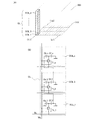
101 第1の配線
102 層間絶縁膜
103 酸化物半導体膜
104 下地絶縁膜
106 酸化物半導体膜
106a チャネル形成領域
106b ソース領域及びドレイン領域
107 レジストマスク
108 ゲート絶縁膜
110 ゲート電極
112 層間絶縁膜
114 第2の配線
130 容量電極
140 第3の配線
200 シリコン基板
201 チャネル形成領域
203 素子分離絶縁層
206 不純物領域
208 ゲート絶縁層
210 ゲート電極
212 層間絶縁膜
214 ドレイン電極
216 層間絶縁膜
300 半導体記憶装置
800 トランジスタ
1141 スイッチング素子
1142 記憶素子
1143 記憶素子群
1189 ROMインターフェース
1190 基板
1191 ALU
1192 ALUコントローラ
1193 インストラクションデコーダ
1194 インタラプトコントローラ
1195 タイミングコントローラ
1196 レジスタ
1197 レジスタコントローラ
1198 バスインターフェース
1199 ROM
9300 筐体
9301 ボタン
9302 マイクロフォン
9303 表示部
9304 スピーカ
9305 カメラ
9310 筐体
9311 表示部
9320 筐体
9321 ボタン
9322 マイクロフォン
9323 表示部
9630 筐体
9631a 表示部
9631b 表示部
9633 留め具
9638 操作スイッチ
Claims (5)
- 第1のメモリセルと、前記第1のメモリセルに積層された第2のメモリセルと、を有し、
前記第1のメモリセルは、第1のトランジスタと、前記第1のトランジスタと電気的に接続された第1の容量及び第2の容量と、を有し、
前記第2のメモリセルは、第2のトランジスタと、前記第2のトランジスタと電気的に接続された第3の容量及び第4の容量と、を有し、
前記第1のトランジスタは、チャネルが形成される第1の酸化物半導体層を有し、
前記第2のトランジスタは、チャネルが形成される第2の酸化物半導体層を有し、
前記第1のトランジスタの第1のゲートは、前記第1の酸化物半導体層の上方に設けられ、
前記第2のトランジスタの第1のゲートは、前記第2の酸化物半導体層の上方に設けられ、
前記第2のトランジスタの第1のゲートは、前記第1の酸化物半導体層の下方に設けられ、
前記第2のトランジスタの第1のゲートは、前記第1のトランジスタの第2のゲートとして機能し、
前記第2のトランジスタの第2のゲートは、前記第2の酸化物半導体層の下方に設けられ、
前記第1の酸化物半導体層は、前記第1の容量の一方の電極、及び、前記第2の容量の一方の電極として機能し、
前記第1の容量の他方の電極は、前記第1のトランジスタの第1のゲートと同層に設けられ、
前記第2の酸化物半導体層は、前記第3の容量の一方の電極、及び、前記第4の容量の一方の電極として機能し、
前記第3の容量の他方の電極は、前記第2のトランジスタの第1のゲートと同層に設けられ、前記第2の容量の他方の電極として機能し、
前記第4の容量の他方の電極は、前記第2のトランジスタの第2のゲートと同層に設けられることを特徴とする半導体記憶装置。 - 第1のメモリセルと、前記第1のメモリセルに積層された第2のメモリセルと、を有し、
前記第1のメモリセルは、第1のトランジスタと、前記第1のトランジスタと電気的に接続された第1の容量及び第2の容量と、を有し、
前記第2のメモリセルは、第2のトランジスタと、前記第2のトランジスタと電気的に接続された第3の容量及び第4の容量と、を有し、
前記第1のトランジスタは、チャネルが形成される第1の酸化物半導体層を有し、
前記第2のトランジスタは、チャネルが形成される第2の酸化物半導体層を有し、
前記第1のトランジスタの第1のゲートは、前記第1の酸化物半導体層の上方に設けられ、
前記第2のトランジスタの第1のゲートは、前記第2の酸化物半導体層の上方に設けられ、
前記第2のトランジスタの第1のゲートは、前記第1の酸化物半導体層の下方に設けられ、
前記第2のトランジスタの第1のゲートは、前記第1のトランジスタの第2のゲートとして機能し、
前記第2のトランジスタの第2のゲートは、前記第2の酸化物半導体層の下方に設けられ、
前記第1のトランジスタの第1のゲートは、前記第2のトランジスタの第1のゲートに電気的に接続され、
前記第1のトランジスタの第1のゲートは、前記第2のトランジスタの第2のゲートに電気的に接続されることを特徴とする半導体記憶装置。 - 請求項2において、
前記第1の酸化物半導体層は、前記第1の容量の一方の電極、及び、前記第2の容量の一方の電極として機能し、
前記第1の容量の他方の電極は、前記第1のトランジスタの第1のゲートと同層に設けられ、
前記第2の酸化物半導体層は、前記第3の容量の一方の電極、及び、前記第4の容量の一方の電極として機能し、
前記第3の容量の他方の電極は、前記第2のトランジスタの第1のゲートと同層に設けられ、前記第2の容量の他方の電極として機能し、
前記第4の容量の他方の電極は、前記第2のトランジスタの第2のゲートと同層に設けられることを特徴とする半導体記憶装置。 - 請求項1乃至請求項3のいずれか一において、
前記第1のトランジスタの第1のゲートは、前記第1のトランジスタのチャネル幅方向において、前記第1の酸化物半導体層の端部を越えて設けられ、
前記第2のトランジスタの第1のゲートは、前記第2のトランジスタのチャネル幅方向において、前記第2の酸化物半導体層の端部を越えて設けられ、且つ、前記第1のトランジスタのチャネル幅方向において、前記第1の酸化物半導体層の端部を越えて設けられ、
前記第2のトランジスタの第2のゲートは、前記第2のトランジスタのチャネル幅方向において、前記第2の酸化物半導体層の端部を越えて設けられることを特徴とする半導体記憶装置。 - 請求項1乃至請求項4のいずれか一において、
前記第1の容量の他方の電極は、前記第1のトランジスタのチャネル幅方向において、前記第1の酸化物半導体層の端部を越えて設けられ、
前記第3の容量の他方の電極は、前記第2のトランジスタのチャネル幅方向において、前記第2の酸化物半導体層の端部を越えて設けられ、且つ、前記第1のトランジスタのチャネル幅方向において、前記第1の酸化物半導体層の端部を越えて設けられ、
前記第4の容量の他方の電極は、前記第2のトランジスタのチャネル幅方向において、前記第2の酸化物半導体層の端部を越えて設けられることを特徴とする半導体記憶装置。
Priority Applications (1)
| Application Number | Priority Date | Filing Date | Title |
|---|---|---|---|
| JP2012277937A JP6121709B2 (ja) | 2011-12-22 | 2012-12-20 | 半導体記憶装置 |
Applications Claiming Priority (3)
| Application Number | Priority Date | Filing Date | Title |
|---|---|---|---|
| JP2011281599 | 2011-12-22 | ||
| JP2011281599 | 2011-12-22 | ||
| JP2012277937A JP6121709B2 (ja) | 2011-12-22 | 2012-12-20 | 半導体記憶装置 |
Related Child Applications (1)
| Application Number | Title | Priority Date | Filing Date |
|---|---|---|---|
| JP2017019287A Division JP6293936B2 (ja) | 2011-12-22 | 2017-02-06 | 半導体記憶装置 |
Publications (3)
| Publication Number | Publication Date |
|---|---|
| JP2013149970A JP2013149970A (ja) | 2013-08-01 |
| JP2013149970A5 JP2013149970A5 (ja) | 2015-11-12 |
| JP6121709B2 true JP6121709B2 (ja) | 2017-04-26 |
Family
ID=48653676
Family Applications (7)
| Application Number | Title | Priority Date | Filing Date |
|---|---|---|---|
| JP2012277937A Active JP6121709B2 (ja) | 2011-12-22 | 2012-12-20 | 半導体記憶装置 |
| JP2017019287A Expired - Fee Related JP6293936B2 (ja) | 2011-12-22 | 2017-02-06 | 半導体記憶装置 |
| JP2018024083A Active JP6567105B2 (ja) | 2011-12-22 | 2018-02-14 | 半導体装置 |
| JP2019139870A Active JP6823695B2 (ja) | 2011-12-22 | 2019-07-30 | 半導体装置 |
| JP2021001992A Active JP7035230B2 (ja) | 2011-12-22 | 2021-01-08 | 半導体装置 |
| JP2022031869A Active JP7291821B2 (ja) | 2011-12-22 | 2022-03-02 | 半導体装置 |
| JP2023092504A Pending JP2023110044A (ja) | 2011-12-22 | 2023-06-05 | 半導体装置 |
Family Applications After (6)
| Application Number | Title | Priority Date | Filing Date |
|---|---|---|---|
| JP2017019287A Expired - Fee Related JP6293936B2 (ja) | 2011-12-22 | 2017-02-06 | 半導体記憶装置 |
| JP2018024083A Active JP6567105B2 (ja) | 2011-12-22 | 2018-02-14 | 半導体装置 |
| JP2019139870A Active JP6823695B2 (ja) | 2011-12-22 | 2019-07-30 | 半導体装置 |
| JP2021001992A Active JP7035230B2 (ja) | 2011-12-22 | 2021-01-08 | 半導体装置 |
| JP2022031869A Active JP7291821B2 (ja) | 2011-12-22 | 2022-03-02 | 半導体装置 |
| JP2023092504A Pending JP2023110044A (ja) | 2011-12-22 | 2023-06-05 | 半導体装置 |
Country Status (2)
| Country | Link |
|---|---|
| US (3) | US8907392B2 (ja) |
| JP (7) | JP6121709B2 (ja) |
Families Citing this family (30)
| Publication number | Priority date | Publication date | Assignee | Title |
|---|---|---|---|---|
| US8642380B2 (en) * | 2010-07-02 | 2014-02-04 | Semiconductor Energy Laboratory Co., Ltd. | Manufacturing method of semiconductor device |
| US8981367B2 (en) | 2011-12-01 | 2015-03-17 | Semiconductor Energy Laboratory Co., Ltd. | Semiconductor device |
| US10002968B2 (en) | 2011-12-14 | 2018-06-19 | Semiconductor Energy Laboratory Co., Ltd. | Semiconductor device and display device including the same |
| US8704221B2 (en) | 2011-12-23 | 2014-04-22 | Semiconductor Energy Laboratory Co., Ltd. | Semiconductor device |
| US9006024B2 (en) | 2012-04-25 | 2015-04-14 | Semiconductor Energy Laboratory Co., Ltd. | Method for manufacturing semiconductor device |
| JP2014045175A (ja) | 2012-08-02 | 2014-03-13 | Semiconductor Energy Lab Co Ltd | 半導体装置 |
| US9515068B1 (en) | 2013-08-29 | 2016-12-06 | Hrl Laboratories, Llc | Monolithic integration of GaN and InP components |
| US9607991B2 (en) | 2013-09-05 | 2017-03-28 | Semiconductor Energy Laboratory Co., Ltd. | Semiconductor device |
| JP6383616B2 (ja) | 2013-09-25 | 2018-08-29 | 株式会社半導体エネルギー研究所 | 半導体装置 |
| CN103500710B (zh) * | 2013-10-11 | 2015-11-25 | 京东方科技集团股份有限公司 | 一种薄膜晶体管制作方法、薄膜晶体管及显示设备 |
| US9443876B2 (en) | 2014-02-05 | 2016-09-13 | Semiconductor Energy Laboratory Co., Ltd. | Semiconductor device, display device including the semiconductor device, display module including the display device, and electronic device including the semiconductor device, the display device, and the display module |
| JP6607681B2 (ja) | 2014-03-07 | 2019-11-20 | 株式会社半導体エネルギー研究所 | 半導体装置 |
| US9087689B1 (en) * | 2014-07-11 | 2015-07-21 | Inoso, Llc | Method of forming a stacked low temperature transistor and related devices |
| JP6801969B2 (ja) * | 2015-03-03 | 2020-12-16 | 株式会社半導体エネルギー研究所 | 半導体装置、表示装置、および電子機器 |
| JP6773453B2 (ja) * | 2015-05-26 | 2020-10-21 | 株式会社半導体エネルギー研究所 | 記憶装置及び電子機器 |
| US9847406B2 (en) | 2015-08-27 | 2017-12-19 | Semiconductor Energy Laboratory Co., Ltd. | Semiconductor device, storage device, resistor circuit, display device, and electronic device |
| JP6811084B2 (ja) | 2015-12-18 | 2021-01-13 | 株式会社半導体エネルギー研究所 | 半導体装置 |
| US10115741B2 (en) * | 2016-02-05 | 2018-10-30 | Semiconductor Energy Laboratory Co., Ltd. | Semiconductor device and electronic device |
| CN106098687B (zh) * | 2016-08-03 | 2019-04-16 | 贵州大学 | 一种三维功率vdmos器件及其集成方法 |
| TWI708329B (zh) * | 2017-03-20 | 2020-10-21 | 聯華電子股份有限公司 | 記憶體元件及其製作方法 |
| KR102268704B1 (ko) | 2017-04-11 | 2021-06-28 | 삼성전자주식회사 | 쓰기 보조 회로를 포함하는 메모리 장치 |
| KR20230021180A (ko) * | 2017-06-27 | 2023-02-13 | 가부시키가이샤 한도오따이 에네루기 켄큐쇼 | 기억 장치 |
| US10535659B2 (en) | 2017-09-29 | 2020-01-14 | Samsung Electronics Co., Ltd. | Semiconductor memory devices |
| KR102524614B1 (ko) | 2017-11-24 | 2023-04-24 | 삼성전자주식회사 | 반도체 메모리 소자 |
| US11342461B2 (en) * | 2018-03-07 | 2022-05-24 | Sharp Kabushiki Kaisha | Thin film transistor, method for producing same and display device |
| JP7433250B2 (ja) * | 2019-01-29 | 2024-02-19 | 株式会社半導体エネルギー研究所 | 記憶装置 |
| KR20200127101A (ko) * | 2019-04-30 | 2020-11-10 | 삼성전자주식회사 | 반도체 메모리 소자 및 이의 제조 방법 |
| KR20210002775A (ko) | 2019-06-27 | 2021-01-11 | 삼성전자주식회사 | 반도체 메모리 소자 |
| KR20220055513A (ko) * | 2020-10-26 | 2022-05-04 | 삼성전자주식회사 | 반도체 메모리 장치 |
| US20230299197A1 (en) * | 2022-03-17 | 2023-09-21 | Renesas Electronics Corporation | Semiconductor device |
Family Cites Families (162)
| Publication number | Priority date | Publication date | Assignee | Title |
|---|---|---|---|---|
| US4555721A (en) | 1981-05-19 | 1985-11-26 | International Business Machines Corporation | Structure of stacked, complementary MOS field effect transistor circuits |
| JPS5837948A (ja) * | 1981-08-31 | 1983-03-05 | Toshiba Corp | 積層半導体記憶装置 |
| JPS60198861A (ja) | 1984-03-23 | 1985-10-08 | Fujitsu Ltd | 薄膜トランジスタ |
| JPS613450A (ja) * | 1984-06-18 | 1986-01-09 | Hiroshima Daigaku | 三次元光結合共有メモリ集積装置 |
| JPS63102264A (ja) | 1986-10-20 | 1988-05-07 | Nissan Motor Co Ltd | 薄膜半導体装置 |
| JPH0244256B2 (ja) | 1987-01-28 | 1990-10-03 | Kagaku Gijutsucho Mukizaishitsu Kenkyushocho | Ingazn2o5deshimesarerurotsuhoshokeinosojokozoojusurukagobutsuoyobisonoseizoho |
| JPH0244260B2 (ja) | 1987-02-24 | 1990-10-03 | Kagaku Gijutsucho Mukizaishitsu Kenkyushocho | Ingazn5o8deshimesarerurotsuhoshokeinosojokozoojusurukagobutsuoyobisonoseizoho |
| JPS63210023A (ja) | 1987-02-24 | 1988-08-31 | Natl Inst For Res In Inorg Mater | InGaZn↓4O↓7で示される六方晶系の層状構造を有する化合物およびその製造法 |
| JPH0244258B2 (ja) | 1987-02-24 | 1990-10-03 | Kagaku Gijutsucho Mukizaishitsu Kenkyushocho | Ingazn3o6deshimesarerurotsuhoshokeinosojokozoojusurukagobutsuoyobisonoseizoho |
| JPH0244262B2 (ja) | 1987-02-27 | 1990-10-03 | Kagaku Gijutsucho Mukizaishitsu Kenkyushocho | Ingazn6o9deshimesarerurotsuhoshokeinosojokozoojusurukagobutsuoyobisonoseizoho |
| JPH0244263B2 (ja) | 1987-04-22 | 1990-10-03 | Kagaku Gijutsucho Mukizaishitsu Kenkyushocho | Ingazn7o10deshimesarerurotsuhoshokeinosojokozoojusurukagobutsuoyobisonoseizoho |
| JPH01246863A (ja) | 1988-03-29 | 1989-10-02 | Seiko Epson Corp | 半導体装置及び製造方法 |
| EP0469217B1 (en) | 1990-07-31 | 1996-04-10 | International Business Machines Corporation | Method of forming stacked self-aligned polysilicon PFET devices and structures resulting therefrom |
| US5095347A (en) | 1990-08-01 | 1992-03-10 | Motorola, Inc. | Plural transistor silicon on insulator structure with shared electrodes |
| JP3015186B2 (ja) | 1991-03-28 | 2000-03-06 | 三菱電機株式会社 | 半導体記憶装置とそのデータの読み出しおよび書き込み方法 |
| JPH05251705A (ja) | 1992-03-04 | 1993-09-28 | Fuji Xerox Co Ltd | 薄膜トランジスタ |
| JPH0613606A (ja) | 1992-06-25 | 1994-01-21 | Victor Co Of Japan Ltd | 半導体装置 |
| JP3298974B2 (ja) | 1993-03-23 | 2002-07-08 | 電子科学株式会社 | 昇温脱離ガス分析装置 |
| JPH06291269A (ja) | 1993-04-06 | 1994-10-18 | Sony Corp | 電界効果トランジスタ |
| JPH0794743A (ja) | 1993-09-20 | 1995-04-07 | Fujitsu Ltd | 半導体装置 |
| KR0169157B1 (ko) | 1993-11-29 | 1999-02-01 | 기다오까 다까시 | 반도체 회로 및 mos-dram |
| JP2734962B2 (ja) | 1993-12-27 | 1998-04-02 | 日本電気株式会社 | 薄膜トランジスタ及びその製造方法 |
| JPH08148693A (ja) | 1994-09-22 | 1996-06-07 | Sanyo Electric Co Ltd | 薄膜トランジスタ及びその製造方法 |
| JP3479375B2 (ja) | 1995-03-27 | 2003-12-15 | 科学技術振興事業団 | 亜酸化銅等の金属酸化物半導体による薄膜トランジスタとpn接合を形成した金属酸化物半導体装置およびそれらの製造方法 |
| EP0820644B1 (en) | 1995-08-03 | 2005-08-24 | Koninklijke Philips Electronics N.V. | Semiconductor device provided with transparent switching element |
| JP3625598B2 (ja) | 1995-12-30 | 2005-03-02 | 三星電子株式会社 | 液晶表示装置の製造方法 |
| JPH09245482A (ja) | 1996-03-08 | 1997-09-19 | Hitachi Ltd | 論理回路及び半導体記憶装置 |
| US5949092A (en) | 1997-08-01 | 1999-09-07 | Advanced Micro Devices, Inc. | Ultra-high-density pass gate using dual stacked transistors having a gate structure with planarized upper surface in relation to interlayer insulator |
| KR100269309B1 (ko) * | 1997-09-29 | 2000-10-16 | 윤종용 | 고집적강유전체메모리장치및그제조방법 |
| JP4170454B2 (ja) | 1998-07-24 | 2008-10-22 | Hoya株式会社 | 透明導電性酸化物薄膜を有する物品及びその製造方法 |
| JP2000150861A (ja) | 1998-11-16 | 2000-05-30 | Tdk Corp | 酸化物薄膜 |
| JP3276930B2 (ja) | 1998-11-17 | 2002-04-22 | 科学技術振興事業団 | トランジスタ及び半導体装置 |
| JP2000323668A (ja) * | 1999-05-14 | 2000-11-24 | Nec Corp | 強誘電体容量及びこれを備えた回路装置 |
| TW460731B (en) | 1999-09-03 | 2001-10-21 | Ind Tech Res Inst | Electrode structure and production method of wide viewing angle LCD |
| JP4089858B2 (ja) | 2000-09-01 | 2008-05-28 | 国立大学法人東北大学 | 半導体デバイス |
| KR20020038482A (ko) | 2000-11-15 | 2002-05-23 | 모리시타 요이찌 | 박막 트랜지스터 어레이, 그 제조방법 및 그것을 이용한표시패널 |
| JP2002184993A (ja) | 2000-12-11 | 2002-06-28 | Sony Corp | 半導体装置 |
| JP3997731B2 (ja) | 2001-03-19 | 2007-10-24 | 富士ゼロックス株式会社 | 基材上に結晶性半導体薄膜を形成する方法 |
| JP2002289859A (ja) | 2001-03-23 | 2002-10-04 | Minolta Co Ltd | 薄膜トランジスタ |
| JP4731718B2 (ja) * | 2001-04-27 | 2011-07-27 | 株式会社半導体エネルギー研究所 | 表示装置 |
| JP3640177B2 (ja) | 2001-06-04 | 2005-04-20 | セイコーエプソン株式会社 | 不揮発性半導体記憶装置 |
| JP3925839B2 (ja) | 2001-09-10 | 2007-06-06 | シャープ株式会社 | 半導体記憶装置およびその試験方法 |
| JP4090716B2 (ja) | 2001-09-10 | 2008-05-28 | 雅司 川崎 | 薄膜トランジスタおよびマトリクス表示装置 |
| JP4164562B2 (ja) | 2002-09-11 | 2008-10-15 | 独立行政法人科学技術振興機構 | ホモロガス薄膜を活性層として用いる透明薄膜電界効果型トランジスタ |
| WO2003040441A1 (en) | 2001-11-05 | 2003-05-15 | Japan Science And Technology Agency | Natural superlattice homologous single crystal thin film, method for preparation thereof, and device using said single crystal thin film |
| JP4275336B2 (ja) * | 2001-11-16 | 2009-06-10 | 株式会社半導体エネルギー研究所 | 半導体装置の作製方法 |
| JP4083486B2 (ja) | 2002-02-21 | 2008-04-30 | 独立行政法人科学技術振興機構 | LnCuO(S,Se,Te)単結晶薄膜の製造方法 |
| US7049190B2 (en) | 2002-03-15 | 2006-05-23 | Sanyo Electric Co., Ltd. | Method for forming ZnO film, method for forming ZnO semiconductor layer, method for fabricating semiconductor device, and semiconductor device |
| JP3933591B2 (ja) | 2002-03-26 | 2007-06-20 | 淳二 城戸 | 有機エレクトロルミネッセント素子 |
| US7339187B2 (en) | 2002-05-21 | 2008-03-04 | State Of Oregon Acting By And Through The Oregon State Board Of Higher Education On Behalf Of Oregon State University | Transistor structures |
| JP2004022625A (ja) | 2002-06-13 | 2004-01-22 | Murata Mfg Co Ltd | 半導体デバイス及び該半導体デバイスの製造方法 |
| US7105868B2 (en) | 2002-06-24 | 2006-09-12 | Cermet, Inc. | High-electron mobility transistor with zinc oxide |
| US7067843B2 (en) | 2002-10-11 | 2006-06-27 | E. I. Du Pont De Nemours And Company | Transparent oxide semiconductor thin film transistors |
| JP4166105B2 (ja) | 2003-03-06 | 2008-10-15 | シャープ株式会社 | 半導体装置およびその製造方法 |
| JP2004273732A (ja) | 2003-03-07 | 2004-09-30 | Sharp Corp | アクティブマトリクス基板およびその製造方法 |
| JP4108633B2 (ja) | 2003-06-20 | 2008-06-25 | シャープ株式会社 | 薄膜トランジスタおよびその製造方法ならびに電子デバイス |
| US7262463B2 (en) | 2003-07-25 | 2007-08-28 | Hewlett-Packard Development Company, L.P. | Transistor including a deposited channel region having a doped portion |
| US7487373B2 (en) | 2004-01-30 | 2009-02-03 | Semiconductor Energy Laboratory Co., Ltd. | Wireless semiconductor device having low power consumption |
| US7282782B2 (en) | 2004-03-12 | 2007-10-16 | Hewlett-Packard Development Company, L.P. | Combined binary oxide semiconductor device |
| KR20070116888A (ko) | 2004-03-12 | 2007-12-11 | 도꾸리쯔교세이호징 가가꾸 기쥬쯔 신꼬 기꼬 | 아몰퍼스 산화물 및 박막 트랜지스터 |
| US7297977B2 (en) | 2004-03-12 | 2007-11-20 | Hewlett-Packard Development Company, L.P. | Semiconductor device |
| US7145174B2 (en) | 2004-03-12 | 2006-12-05 | Hewlett-Packard Development Company, Lp. | Semiconductor device |
| US7211825B2 (en) | 2004-06-14 | 2007-05-01 | Yi-Chi Shih | Indium oxide-based thin film transistors and circuits |
| JP2006100760A (ja) | 2004-09-02 | 2006-04-13 | Casio Comput Co Ltd | 薄膜トランジスタおよびその製造方法 |
| US7285501B2 (en) | 2004-09-17 | 2007-10-23 | Hewlett-Packard Development Company, L.P. | Method of forming a solution processed device |
| US7298084B2 (en) | 2004-11-02 | 2007-11-20 | 3M Innovative Properties Company | Methods and displays utilizing integrated zinc oxide row and column drivers in conjunction with organic light emitting diodes |
| EP1815530B1 (en) | 2004-11-10 | 2021-02-17 | Canon Kabushiki Kaisha | Field effect transistor employing an amorphous oxide |
| BRPI0517568B8 (pt) | 2004-11-10 | 2022-03-03 | Canon Kk | Transistor de efeito de campo |
| US7453065B2 (en) | 2004-11-10 | 2008-11-18 | Canon Kabushiki Kaisha | Sensor and image pickup device |
| US7791072B2 (en) | 2004-11-10 | 2010-09-07 | Canon Kabushiki Kaisha | Display |
| US7863611B2 (en) | 2004-11-10 | 2011-01-04 | Canon Kabushiki Kaisha | Integrated circuits utilizing amorphous oxides |
| US7829444B2 (en) | 2004-11-10 | 2010-11-09 | Canon Kabushiki Kaisha | Field effect transistor manufacturing method |
| JP5118811B2 (ja) * | 2004-11-10 | 2013-01-16 | キヤノン株式会社 | 発光装置及び表示装置 |
| US7579224B2 (en) | 2005-01-21 | 2009-08-25 | Semiconductor Energy Laboratory Co., Ltd. | Method for manufacturing a thin film semiconductor device |
| TWI412138B (zh) | 2005-01-28 | 2013-10-11 | Semiconductor Energy Lab | 半導體裝置,電子裝置,和半導體裝置的製造方法 |
| US7608531B2 (en) | 2005-01-28 | 2009-10-27 | Semiconductor Energy Laboratory Co., Ltd. | Semiconductor device, electronic device, and method of manufacturing semiconductor device |
| US7858451B2 (en) | 2005-02-03 | 2010-12-28 | Semiconductor Energy Laboratory Co., Ltd. | Electronic device, semiconductor device and manufacturing method thereof |
| US7948171B2 (en) | 2005-02-18 | 2011-05-24 | Semiconductor Energy Laboratory Co., Ltd. | Light emitting device |
| JP4586573B2 (ja) * | 2005-02-28 | 2010-11-24 | エプソンイメージングデバイス株式会社 | 電気光学装置及びその製造方法、薄膜トランジスタ、電子機器 |
| US20060197092A1 (en) | 2005-03-03 | 2006-09-07 | Randy Hoffman | System and method for forming conductive material on a substrate |
| US8681077B2 (en) | 2005-03-18 | 2014-03-25 | Semiconductor Energy Laboratory Co., Ltd. | Semiconductor device, and display device, driving method and electronic apparatus thereof |
| WO2006105077A2 (en) | 2005-03-28 | 2006-10-05 | Massachusetts Institute Of Technology | Low voltage thin film transistor with high-k dielectric material |
| US7645478B2 (en) | 2005-03-31 | 2010-01-12 | 3M Innovative Properties Company | Methods of making displays |
| US8300031B2 (en) | 2005-04-20 | 2012-10-30 | Semiconductor Energy Laboratory Co., Ltd. | Semiconductor device comprising transistor having gate and drain connected through a current-voltage conversion element |
| JP2006344849A (ja) | 2005-06-10 | 2006-12-21 | Casio Comput Co Ltd | 薄膜トランジスタ |
| US7691666B2 (en) | 2005-06-16 | 2010-04-06 | Eastman Kodak Company | Methods of making thin film transistors comprising zinc-oxide-based semiconductor materials and transistors made thereby |
| US7402506B2 (en) | 2005-06-16 | 2008-07-22 | Eastman Kodak Company | Methods of making thin film transistors comprising zinc-oxide-based semiconductor materials and transistors made thereby |
| US7507618B2 (en) | 2005-06-27 | 2009-03-24 | 3M Innovative Properties Company | Method for making electronic devices using metal oxide nanoparticles |
| KR100711890B1 (ko) | 2005-07-28 | 2007-04-25 | 삼성에스디아이 주식회사 | 유기 발광표시장치 및 그의 제조방법 |
| JP2007059128A (ja) | 2005-08-23 | 2007-03-08 | Canon Inc | 有機el表示装置およびその製造方法 |
| JP4280736B2 (ja) | 2005-09-06 | 2009-06-17 | キヤノン株式会社 | 半導体素子 |
| JP4732080B2 (ja) * | 2005-09-06 | 2011-07-27 | キヤノン株式会社 | 発光素子 |
| JP2007073705A (ja) | 2005-09-06 | 2007-03-22 | Canon Inc | 酸化物半導体チャネル薄膜トランジスタおよびその製造方法 |
| JP5116225B2 (ja) | 2005-09-06 | 2013-01-09 | キヤノン株式会社 | 酸化物半導体デバイスの製造方法 |
| JP4850457B2 (ja) | 2005-09-06 | 2012-01-11 | キヤノン株式会社 | 薄膜トランジスタ及び薄膜ダイオード |
| EP1998375A3 (en) | 2005-09-29 | 2012-01-18 | Semiconductor Energy Laboratory Co, Ltd. | Semiconductor device having oxide semiconductor layer and manufacturing method |
| JP5037808B2 (ja) | 2005-10-20 | 2012-10-03 | キヤノン株式会社 | アモルファス酸化物を用いた電界効果型トランジスタ、及び該トランジスタを用いた表示装置 |
| KR101358954B1 (ko) | 2005-11-15 | 2014-02-06 | 가부시키가이샤 한도오따이 에네루기 켄큐쇼 | 다이오드 및 액티브 매트릭스 표시장치 |
| TWI292281B (en) | 2005-12-29 | 2008-01-01 | Ind Tech Res Inst | Pixel structure of active organic light emitting diode and method of fabricating the same |
| US7867636B2 (en) | 2006-01-11 | 2011-01-11 | Murata Manufacturing Co., Ltd. | Transparent conductive film and method for manufacturing the same |
| JP4977478B2 (ja) | 2006-01-21 | 2012-07-18 | 三星電子株式会社 | ZnOフィルム及びこれを用いたTFTの製造方法 |
| US7576394B2 (en) | 2006-02-02 | 2009-08-18 | Kochi Industrial Promotion Center | Thin film transistor including low resistance conductive thin films and manufacturing method thereof |
| US7977169B2 (en) | 2006-02-15 | 2011-07-12 | Kochi Industrial Promotion Center | Semiconductor device including active layer made of zinc oxide with controlled orientations and manufacturing method thereof |
| KR20070101595A (ko) | 2006-04-11 | 2007-10-17 | 삼성전자주식회사 | ZnO TFT |
| US20070252928A1 (en) | 2006-04-28 | 2007-11-01 | Toppan Printing Co., Ltd. | Structure, transmission type liquid crystal display, reflection type display and manufacturing method thereof |
| JP5028033B2 (ja) | 2006-06-13 | 2012-09-19 | キヤノン株式会社 | 酸化物半導体膜のドライエッチング方法 |
| JP4609797B2 (ja) | 2006-08-09 | 2011-01-12 | Nec液晶テクノロジー株式会社 | 薄膜デバイス及びその製造方法 |
| JP5045022B2 (ja) | 2006-08-09 | 2012-10-10 | 富士通セミコンダクター株式会社 | 半導体記憶装置 |
| JP4999400B2 (ja) | 2006-08-09 | 2012-08-15 | キヤノン株式会社 | 酸化物半導体膜のドライエッチング方法 |
| JP4179393B2 (ja) | 2006-09-14 | 2008-11-12 | エプソンイメージングデバイス株式会社 | 表示装置及びその製造方法 |
| JP4332545B2 (ja) | 2006-09-15 | 2009-09-16 | キヤノン株式会社 | 電界効果型トランジスタ及びその製造方法 |
| JP5164357B2 (ja) | 2006-09-27 | 2013-03-21 | キヤノン株式会社 | 半導体装置及び半導体装置の製造方法 |
| JP4274219B2 (ja) | 2006-09-27 | 2009-06-03 | セイコーエプソン株式会社 | 電子デバイス、有機エレクトロルミネッセンス装置、有機薄膜半導体装置 |
| US7622371B2 (en) | 2006-10-10 | 2009-11-24 | Hewlett-Packard Development Company, L.P. | Fused nanocrystal thin film semiconductor and method |
| US7772021B2 (en) | 2006-11-29 | 2010-08-10 | Samsung Electronics Co., Ltd. | Flat panel displays comprising a thin-film transistor having a semiconductive oxide in its channel and methods of fabricating the same for use in flat panel displays |
| JP2008140912A (ja) * | 2006-11-30 | 2008-06-19 | Toshiba Corp | 不揮発性半導体記憶装置 |
| JP2008140684A (ja) | 2006-12-04 | 2008-06-19 | Toppan Printing Co Ltd | カラーelディスプレイおよびその製造方法 |
| KR101303578B1 (ko) | 2007-01-05 | 2013-09-09 | 삼성전자주식회사 | 박막 식각 방법 |
| US8207063B2 (en) | 2007-01-26 | 2012-06-26 | Eastman Kodak Company | Process for atomic layer deposition |
| KR100851215B1 (ko) | 2007-03-14 | 2008-08-07 | 삼성에스디아이 주식회사 | 박막 트랜지스터 및 이를 이용한 유기 전계 발광표시장치 |
| US7795613B2 (en) | 2007-04-17 | 2010-09-14 | Toppan Printing Co., Ltd. | Structure with transistor |
| KR101325053B1 (ko) | 2007-04-18 | 2013-11-05 | 삼성디스플레이 주식회사 | 박막 트랜지스터 기판 및 이의 제조 방법 |
| KR20080094300A (ko) | 2007-04-19 | 2008-10-23 | 삼성전자주식회사 | 박막 트랜지스터 및 그 제조 방법과 박막 트랜지스터를포함하는 평판 디스플레이 |
| KR101334181B1 (ko) | 2007-04-20 | 2013-11-28 | 삼성전자주식회사 | 선택적으로 결정화된 채널층을 갖는 박막 트랜지스터 및 그제조 방법 |
| WO2008133345A1 (en) | 2007-04-25 | 2008-11-06 | Canon Kabushiki Kaisha | Oxynitride semiconductor |
| JP5288391B2 (ja) | 2007-05-24 | 2013-09-11 | ルネサスエレクトロニクス株式会社 | 半導体記憶装置 |
| KR101345376B1 (ko) | 2007-05-29 | 2013-12-24 | 삼성전자주식회사 | ZnO 계 박막 트랜지스터 및 그 제조방법 |
| CN101689532B (zh) | 2007-06-29 | 2013-06-12 | 株式会社半导体能源研究所 | 半导体器件及其制造方法 |
| US8049253B2 (en) | 2007-07-11 | 2011-11-01 | Semiconductor Energy Laboratory Co., Ltd. | Semiconductor device and method for manufacturing the same |
| JP5430846B2 (ja) * | 2007-12-03 | 2014-03-05 | 株式会社半導体エネルギー研究所 | 半導体装置の作製方法 |
| JP5215158B2 (ja) | 2007-12-17 | 2013-06-19 | 富士フイルム株式会社 | 無機結晶性配向膜及びその製造方法、半導体デバイス |
| JP5537020B2 (ja) * | 2008-01-18 | 2014-07-02 | ルネサスエレクトロニクス株式会社 | 不揮発性半導体記憶装置 |
| KR101496148B1 (ko) * | 2008-05-15 | 2015-02-27 | 삼성전자주식회사 | 반도체소자 및 그 제조방법 |
| JP2010016100A (ja) | 2008-07-02 | 2010-01-21 | Toshiba Corp | 半導体記憶装置 |
| JP4623179B2 (ja) | 2008-09-18 | 2011-02-02 | ソニー株式会社 | 薄膜トランジスタおよびその製造方法 |
| KR101623958B1 (ko) * | 2008-10-01 | 2016-05-25 | 삼성전자주식회사 | 인버터 및 그의 동작방법과 인버터를 포함하는 논리회로 |
| JP5451280B2 (ja) | 2008-10-09 | 2014-03-26 | キヤノン株式会社 | ウルツ鉱型結晶成長用基板およびその製造方法ならびに半導体装置 |
| CN102422426B (zh) | 2009-05-01 | 2016-06-01 | 株式会社半导体能源研究所 | 半导体装置的制造方法 |
| JP2010263211A (ja) * | 2009-05-04 | 2010-11-18 | Samsung Electronics Co Ltd | 積層メモリ素子 |
| WO2011007677A1 (en) * | 2009-07-17 | 2011-01-20 | Semiconductor Energy Laboratory Co., Ltd. | Semiconductor device and method for manufacturing the same |
| JP5685805B2 (ja) | 2009-07-23 | 2015-03-18 | セイコーエプソン株式会社 | 半導体装置、半導体装置の製造方法、および電子機器 |
| FR2949904B1 (fr) * | 2009-09-07 | 2012-01-06 | Commissariat Energie Atomique | Circuit integre a transistors mos couples electrostatiquement et procede de realisation d'un tel circuit integre |
| JP5044624B2 (ja) * | 2009-09-25 | 2012-10-10 | 株式会社東芝 | 不揮発性半導体記憶装置 |
| JP2011091110A (ja) | 2009-10-20 | 2011-05-06 | Canon Inc | 酸化物半導体素子を用いた回路及びその製造方法、並びに表示装置 |
| KR101490726B1 (ko) | 2009-10-21 | 2015-02-09 | 가부시키가이샤 한도오따이 에네루기 켄큐쇼 | 반도체 장치 |
| CN102640279B (zh) * | 2009-10-30 | 2015-06-17 | 株式会社半导体能源研究所 | 半导体器件 |
| WO2011074407A1 (en) * | 2009-12-18 | 2011-06-23 | Semiconductor Energy Laboratory Co., Ltd. | Semiconductor device and method for manufacturing the same |
| EP2517245B1 (en) * | 2009-12-25 | 2019-07-24 | Semiconductor Energy Laboratory Co. Ltd. | Semiconductor device |
| CN102804360B (zh) | 2009-12-25 | 2014-12-17 | 株式会社半导体能源研究所 | 半导体装置 |
| CN102656691B (zh) | 2009-12-28 | 2015-07-29 | 株式会社半导体能源研究所 | 存储器装置和半导体装置 |
| KR101855060B1 (ko) * | 2010-01-22 | 2018-05-09 | 가부시키가이샤 한도오따이 에네루기 켄큐쇼 | 반도체 메모리 장치 및 그 구동 방법 |
| KR101820776B1 (ko) * | 2010-02-19 | 2018-01-22 | 가부시키가이샤 한도오따이 에네루기 켄큐쇼 | 반도체 장치 |
| WO2011125806A1 (en) * | 2010-04-09 | 2011-10-13 | Semiconductor Energy Laboratory Co., Ltd. | Manufacturing method of semiconductor device |
| US20120032165A1 (en) * | 2010-08-06 | 2012-02-09 | Korea Advanced Institute Of Science And Technology | Aqueous solution composition for fluorine doped metal oxide semiconductor and thin film transistor including the same |
| CN103201831B (zh) | 2010-11-05 | 2015-08-05 | 株式会社半导体能源研究所 | 半导体装置 |
| JP5993141B2 (ja) | 2010-12-28 | 2016-09-14 | 株式会社半導体エネルギー研究所 | 記憶装置 |
| US8785923B2 (en) | 2011-04-29 | 2014-07-22 | Semiconductor Energy Laboratory Co., Ltd. | Semiconductor device |
| US20120299074A1 (en) * | 2011-05-24 | 2012-11-29 | Sharp Kabushiki Kaisha | Semiconductor device |
| US8891285B2 (en) | 2011-06-10 | 2014-11-18 | Semiconductor Energy Laboratory Co., Ltd. | Semiconductor memory device |
| US8981367B2 (en) | 2011-12-01 | 2015-03-17 | Semiconductor Energy Laboratory Co., Ltd. | Semiconductor device |
| US10002968B2 (en) | 2011-12-14 | 2018-06-19 | Semiconductor Energy Laboratory Co., Ltd. | Semiconductor device and display device including the same |
| US8704221B2 (en) | 2011-12-23 | 2014-04-22 | Semiconductor Energy Laboratory Co., Ltd. | Semiconductor device |
-
2012
- 2012-12-18 US US13/718,426 patent/US8907392B2/en active Active
- 2012-12-20 JP JP2012277937A patent/JP6121709B2/ja active Active
-
2014
- 2014-12-02 US US14/557,506 patent/US9368501B2/en active Active
-
2016
- 2016-06-10 US US15/179,049 patent/US20160293605A1/en not_active Abandoned
-
2017
- 2017-02-06 JP JP2017019287A patent/JP6293936B2/ja not_active Expired - Fee Related
-
2018
- 2018-02-14 JP JP2018024083A patent/JP6567105B2/ja active Active
-
2019
- 2019-07-30 JP JP2019139870A patent/JP6823695B2/ja active Active
-
2021
- 2021-01-08 JP JP2021001992A patent/JP7035230B2/ja active Active
-
2022
- 2022-03-02 JP JP2022031869A patent/JP7291821B2/ja active Active
-
2023
- 2023-06-05 JP JP2023092504A patent/JP2023110044A/ja active Pending
Also Published As
| Publication number | Publication date |
|---|---|
| US9368501B2 (en) | 2016-06-14 |
| JP2018107464A (ja) | 2018-07-05 |
| JP6567105B2 (ja) | 2019-08-28 |
| JP2021064806A (ja) | 2021-04-22 |
| JP6823695B2 (ja) | 2021-02-03 |
| US20130161713A1 (en) | 2013-06-27 |
| JP2017118127A (ja) | 2017-06-29 |
| JP2019204968A (ja) | 2019-11-28 |
| JP2013149970A (ja) | 2013-08-01 |
| JP2022088391A (ja) | 2022-06-14 |
| JP2023110044A (ja) | 2023-08-08 |
| JP6293936B2 (ja) | 2018-03-14 |
| US20160293605A1 (en) | 2016-10-06 |
| JP7291821B2 (ja) | 2023-06-15 |
| US8907392B2 (en) | 2014-12-09 |
| JP7035230B2 (ja) | 2022-03-14 |
| US20150129872A1 (en) | 2015-05-14 |
Similar Documents
| Publication | Publication Date | Title |
|---|---|---|
| JP7291821B2 (ja) | 半導体装置 | |
| TWI615980B (zh) | 半導體裝置以及半導體裝置的製造方法 | |
| JP6268264B2 (ja) | 半導体装置の作製方法 | |
| US9960279B2 (en) | Semiconductor device and manufacturing method thereof | |
| US20150014683A1 (en) | Semiconductor device | |
| JP6080563B2 (ja) | 半導体装置の作製方法 | |
| JP6013676B2 (ja) | 半導体装置及び半導体装置の作製方法 | |
| US8878270B2 (en) | Semiconductor memory device | |
| US9123692B2 (en) | Semiconductor device and method of manufacturing semiconductor device | |
| JP5881388B2 (ja) | 半導体装置及び半導体装置の作製方法 | |
| JP2013089875A (ja) | 半導体装置およびその作製方法 | |
| JP5912444B2 (ja) | 半導体装置の作製方法 | |
| JP6268248B2 (ja) | トランジスタの作製方法 | |
| JP6194147B2 (ja) | 半導体装置 | |
| JP7209043B2 (ja) | 半導体装置 | |
| JP6246260B2 (ja) | 半導体装置 | |
| JP2019192925A (ja) | 半導体装置 | |
| JP2018026595A (ja) | 半導体装置 |
Legal Events
| Date | Code | Title | Description |
|---|---|---|---|
| A521 | Request for written amendment filed |
Free format text: JAPANESE INTERMEDIATE CODE: A523 Effective date: 20150924 |
|
| A621 | Written request for application examination |
Free format text: JAPANESE INTERMEDIATE CODE: A621 Effective date: 20150924 |
|
| A977 | Report on retrieval |
Free format text: JAPANESE INTERMEDIATE CODE: A971007 Effective date: 20160826 |
|
| A131 | Notification of reasons for refusal |
Free format text: JAPANESE INTERMEDIATE CODE: A131 Effective date: 20160906 |
|
| A521 | Request for written amendment filed |
Free format text: JAPANESE INTERMEDIATE CODE: A523 Effective date: 20161006 |
|
| A02 | Decision of refusal |
Free format text: JAPANESE INTERMEDIATE CODE: A02 Effective date: 20170117 |
|
| A521 | Request for written amendment filed |
Free format text: JAPANESE INTERMEDIATE CODE: A523 Effective date: 20170206 |
|
| A911 | Transfer to examiner for re-examination before appeal (zenchi) |
Free format text: JAPANESE INTERMEDIATE CODE: A911 Effective date: 20170214 |
|
| TRDD | Decision of grant or rejection written | ||
| A01 | Written decision to grant a patent or to grant a registration (utility model) |
Free format text: JAPANESE INTERMEDIATE CODE: A01 Effective date: 20170314 |
|
| A61 | First payment of annual fees (during grant procedure) |
Free format text: JAPANESE INTERMEDIATE CODE: A61 Effective date: 20170330 |
|
| R150 | Certificate of patent or registration of utility model |
Ref document number: 6121709 Country of ref document: JP Free format text: JAPANESE INTERMEDIATE CODE: R150 |
|
| R250 | Receipt of annual fees |
Free format text: JAPANESE INTERMEDIATE CODE: R250 |