JP5616552B2 - フォトダイオードアレイ - Google Patents
フォトダイオードアレイ Download PDFInfo
- Publication number
- JP5616552B2 JP5616552B2 JP2014090297A JP2014090297A JP5616552B2 JP 5616552 B2 JP5616552 B2 JP 5616552B2 JP 2014090297 A JP2014090297 A JP 2014090297A JP 2014090297 A JP2014090297 A JP 2014090297A JP 5616552 B2 JP5616552 B2 JP 5616552B2
- Authority
- JP
- Japan
- Prior art keywords
- semiconductor layer
- photodiode array
- light
- type semiconductor
- insulating film
- Prior art date
- Legal status (The legal status is an assumption and is not a legal conclusion. Google has not performed a legal analysis and makes no representation as to the accuracy of the status listed.)
- Active
Links
Images


Classifications
-
- H—ELECTRICITY
- H10—SEMICONDUCTOR DEVICES; ELECTRIC SOLID-STATE DEVICES NOT OTHERWISE PROVIDED FOR
- H10F—INORGANIC SEMICONDUCTOR DEVICES SENSITIVE TO INFRARED RADIATION, LIGHT, ELECTROMAGNETIC RADIATION OF SHORTER WAVELENGTH OR CORPUSCULAR RADIATION
- H10F39/00—Integrated devices, or assemblies of multiple devices, comprising at least one element covered by group H10F30/00, e.g. radiation detectors comprising photodiode arrays
- H10F39/10—Integrated devices
- H10F39/107—Integrated devices having multiple elements covered by H10F30/00 in a repetitive configuration, e.g. radiation detectors comprising photodiode arrays
-
- H—ELECTRICITY
- H10—SEMICONDUCTOR DEVICES; ELECTRIC SOLID-STATE DEVICES NOT OTHERWISE PROVIDED FOR
- H10F—INORGANIC SEMICONDUCTOR DEVICES SENSITIVE TO INFRARED RADIATION, LIGHT, ELECTROMAGNETIC RADIATION OF SHORTER WAVELENGTH OR CORPUSCULAR RADIATION
- H10F30/00—Individual radiation-sensitive semiconductor devices in which radiation controls the flow of current through the devices, e.g. photodetectors
- H10F30/20—Individual radiation-sensitive semiconductor devices in which radiation controls the flow of current through the devices, e.g. photodetectors the devices having potential barriers, e.g. phototransistors
- H10F30/21—Individual radiation-sensitive semiconductor devices in which radiation controls the flow of current through the devices, e.g. photodetectors the devices having potential barriers, e.g. phototransistors the devices being sensitive to infrared, visible or ultraviolet radiation
- H10F30/22—Individual radiation-sensitive semiconductor devices in which radiation controls the flow of current through the devices, e.g. photodetectors the devices having potential barriers, e.g. phototransistors the devices being sensitive to infrared, visible or ultraviolet radiation the devices having only one potential barrier, e.g. photodiodes
- H10F30/225—Individual radiation-sensitive semiconductor devices in which radiation controls the flow of current through the devices, e.g. photodetectors the devices having potential barriers, e.g. phototransistors the devices being sensitive to infrared, visible or ultraviolet radiation the devices having only one potential barrier, e.g. photodiodes the potential barrier working in avalanche mode, e.g. avalanche photodiodes
-
- H—ELECTRICITY
- H10—SEMICONDUCTOR DEVICES; ELECTRIC SOLID-STATE DEVICES NOT OTHERWISE PROVIDED FOR
- H10F—INORGANIC SEMICONDUCTOR DEVICES SENSITIVE TO INFRARED RADIATION, LIGHT, ELECTROMAGNETIC RADIATION OF SHORTER WAVELENGTH OR CORPUSCULAR RADIATION
- H10F39/00—Integrated devices, or assemblies of multiple devices, comprising at least one element covered by group H10F30/00, e.g. radiation detectors comprising photodiode arrays
- H10F39/80—Constructional details of image sensors
- H10F39/802—Geometry or disposition of elements in pixels, e.g. address-lines or gate electrodes
- H10F39/8023—Disposition of the elements in pixels, e.g. smaller elements in the centre of the imager compared to larger elements at the periphery
-
- H—ELECTRICITY
- H10—SEMICONDUCTOR DEVICES; ELECTRIC SOLID-STATE DEVICES NOT OTHERWISE PROVIDED FOR
- H10F—INORGANIC SEMICONDUCTOR DEVICES SENSITIVE TO INFRARED RADIATION, LIGHT, ELECTROMAGNETIC RADIATION OF SHORTER WAVELENGTH OR CORPUSCULAR RADIATION
- H10F39/00—Integrated devices, or assemblies of multiple devices, comprising at least one element covered by group H10F30/00, e.g. radiation detectors comprising photodiode arrays
- H10F39/80—Constructional details of image sensors
- H10F39/811—Interconnections
-
- H—ELECTRICITY
- H10—SEMICONDUCTOR DEVICES; ELECTRIC SOLID-STATE DEVICES NOT OTHERWISE PROVIDED FOR
- H10F—INORGANIC SEMICONDUCTOR DEVICES SENSITIVE TO INFRARED RADIATION, LIGHT, ELECTROMAGNETIC RADIATION OF SHORTER WAVELENGTH OR CORPUSCULAR RADIATION
- H10F99/00—Subject matter not provided for in other groups of this subclass
-
- H—ELECTRICITY
- H10—SEMICONDUCTOR DEVICES; ELECTRIC SOLID-STATE DEVICES NOT OTHERWISE PROVIDED FOR
- H10F—INORGANIC SEMICONDUCTOR DEVICES SENSITIVE TO INFRARED RADIATION, LIGHT, ELECTROMAGNETIC RADIATION OF SHORTER WAVELENGTH OR CORPUSCULAR RADIATION
- H10F39/00—Integrated devices, or assemblies of multiple devices, comprising at least one element covered by group H10F30/00, e.g. radiation detectors comprising photodiode arrays
- H10F39/80—Constructional details of image sensors
- H10F39/802—Geometry or disposition of elements in pixels, e.g. address-lines or gate electrodes
Landscapes
- Light Receiving Elements (AREA)
- Solid State Image Pick-Up Elements (AREA)
- Physics & Mathematics (AREA)
- Electromagnetism (AREA)
Description
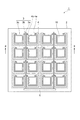
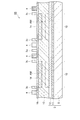
図1及び図2を参照して、第1実施形態に係るフォトダイオードアレイ1の構成について説明する。図1は、第1実施形態に係るフォトダイオードアレイ1の上面を概略的に示す図である。図2は、図1に示したフォトダイオードアレイ1のII−II矢印断面の一部を示す図である。
図6を参照して、第2実施形態に係るフォトダイオードアレイ30の構成について説明する。図6は、第2実施形態に係るフォトダイオードアレイ30の断面図である。第2実施形態に係るフォトダイオードアレイ30は、分離部20が遮光部を有している点で第1実施形態に係るフォトダイオードアレイ1と異なる。
図7を参照して、第3実施形態に係るフォトダイオードアレイ40の構成について説明する。図7は、第3実施形態に係るフォトダイオードアレイ40の断面構造を概略的に説明するための図である。第3実施形態に係るフォトダイオードアレイ40は、信号導線3が窒化シリコン膜上に形成されている点で第1実施形態に係るフォトダイオードアレイ1と異なる。
図8を参照して、第4実施形態に係るフォトダイオードアレイ50の構成について説明する。図8は、第4実施形態に係るフォトダイオードアレイ50の断面図である。第4実施形態に係るフォトダイオードアレイ50は、分離部20を備えていない点で第1実施形態に係るフォトダイオードアレイ1と異なる。
Claims (5)
- ガイガーモードで動作する複数のアバランシェフォトダイオードを配列してなるフォトダイオードアレイにおいて、
前記アバランシェフォトダイオードが形成された基板と、
前記基板上に形成された第1の絶縁膜と、
前記第1の絶縁膜上に形成された第2の絶縁膜と、
前記第2の絶縁膜上に設けられた信号導線と、
前記アバランシェフォトダイオードと前記信号導線とを接続し、前記第1の絶縁膜と前記第2の絶縁膜との間に介在する抵抗と、
を備えることを特徴とするフォトダイオードアレイ。 - 前記信号導線は、アルミニウムからなり、
前記第2の絶縁膜は、窒化シリコンからなる、ことを特徴とする請求項1に記載のフォトダイオードアレイ。 - 前記抵抗は、ポリシリコンからなり、
前記第1の絶縁膜は、酸化シリコンからなる、ことを特徴とする請求項1又は2に記載のフォトダイオードアレイ。 - 第1導電型の第1の半導体層と、
前記第1の半導体層上に形成された第2導電型の第2の半導体層と、
前記第2の半導体層上に形成された第2導電型の第3の半導体層と、を備え、
前記第1の絶縁膜は、前記第3の半導体層上に形成されている、ことを特徴とする請求項1〜3のいずれか一項に記載のフォトダイオードアレイ。 - 第1導電型の第1の半導体層と、
前記第1の半導体層上に形成された第1導電型の第2の半導体層と、
前記第2の半導体層上に形成された第2導電型の第3の半導体層と、を備え、
前記第1の絶縁膜は、前記第3の半導体層上に形成されている、
ことを特徴とする請求項1〜3のいずれか一項に記載のフォトダイオードアレイ。
Priority Applications (1)
| Application Number | Priority Date | Filing Date | Title |
|---|---|---|---|
| JP2014090297A JP5616552B2 (ja) | 2006-07-03 | 2014-04-24 | フォトダイオードアレイ |
Applications Claiming Priority (3)
| Application Number | Priority Date | Filing Date | Title |
|---|---|---|---|
| JP2006183598 | 2006-07-03 | ||
| JP2006183598 | 2006-07-03 | ||
| JP2014090297A JP5616552B2 (ja) | 2006-07-03 | 2014-04-24 | フォトダイオードアレイ |
Related Parent Applications (1)
| Application Number | Title | Priority Date | Filing Date |
|---|---|---|---|
| JP2012238222A Division JP5536853B2 (ja) | 2006-07-03 | 2012-10-29 | フォトダイオードアレイ |
Related Child Applications (1)
| Application Number | Title | Priority Date | Filing Date |
|---|---|---|---|
| JP2014185233A Division JP5952362B2 (ja) | 2006-07-03 | 2014-09-11 | フォトダイオードアレイ |
Publications (2)
| Publication Number | Publication Date |
|---|---|
| JP2014143443A JP2014143443A (ja) | 2014-08-07 |
| JP5616552B2 true JP5616552B2 (ja) | 2014-10-29 |
Family
ID=38894515
Family Applications (6)
| Application Number | Title | Priority Date | Filing Date |
|---|---|---|---|
| JP2008523687A Active JP5183471B2 (ja) | 2006-07-03 | 2007-07-03 | フォトダイオードアレイ |
| JP2012238222A Active JP5536853B2 (ja) | 2006-07-03 | 2012-10-29 | フォトダイオードアレイ |
| JP2014090297A Active JP5616552B2 (ja) | 2006-07-03 | 2014-04-24 | フォトダイオードアレイ |
| JP2014185233A Active JP5952362B2 (ja) | 2006-07-03 | 2014-09-11 | フォトダイオードアレイ |
| JP2016115483A Active JP6134844B2 (ja) | 2006-07-03 | 2016-06-09 | フォトダイオードアレイ |
| JP2017085367A Active JP6454373B2 (ja) | 2006-07-03 | 2017-04-24 | フォトダイオードアレイ |
Family Applications Before (2)
| Application Number | Title | Priority Date | Filing Date |
|---|---|---|---|
| JP2008523687A Active JP5183471B2 (ja) | 2006-07-03 | 2007-07-03 | フォトダイオードアレイ |
| JP2012238222A Active JP5536853B2 (ja) | 2006-07-03 | 2012-10-29 | フォトダイオードアレイ |
Family Applications After (3)
| Application Number | Title | Priority Date | Filing Date |
|---|---|---|---|
| JP2014185233A Active JP5952362B2 (ja) | 2006-07-03 | 2014-09-11 | フォトダイオードアレイ |
| JP2016115483A Active JP6134844B2 (ja) | 2006-07-03 | 2016-06-09 | フォトダイオードアレイ |
| JP2017085367A Active JP6454373B2 (ja) | 2006-07-03 | 2017-04-24 | フォトダイオードアレイ |
Country Status (6)
| Country | Link |
|---|---|
| US (5) | US8008741B2 (ja) |
| EP (2) | EP3002794B1 (ja) |
| JP (6) | JP5183471B2 (ja) |
| CN (1) | CN101484999B (ja) |
| TW (3) | TWI615954B (ja) |
| WO (1) | WO2008004547A1 (ja) |
Cited By (3)
| Publication number | Priority date | Publication date | Assignee | Title |
|---|---|---|---|---|
| US10497823B2 (en) | 2018-03-14 | 2019-12-03 | Kabushiki Kaisha Toshiba | Light receiving device and method of manufacturing light receiving device |
| US11398544B2 (en) | 2019-09-18 | 2022-07-26 | Kabushiki Kaisha Toshiba | Light detector, light detection system, lidar device, and vehicle |
| US12009442B2 (en) | 2021-01-14 | 2024-06-11 | Kabushiki Kaisha Toshiba | Light detector, light detection system, lidar device, and moving body |
Families Citing this family (120)
| Publication number | Priority date | Publication date | Assignee | Title |
|---|---|---|---|---|
| RU2290721C2 (ru) | 2004-05-05 | 2006-12-27 | Борис Анатольевич Долгошеин | Кремниевый фотоэлектронный умножитель (варианты) и ячейка для кремниевого фотоэлектронного умножителя |
| CN102066976A (zh) * | 2008-06-16 | 2011-05-18 | 皇家飞利浦电子股份有限公司 | 辐射探测器和制造辐射探测器的方法 |
| US8279411B2 (en) * | 2008-08-27 | 2012-10-02 | The Boeing Company | Systems and methods for reducing crosstalk in an avalanche photodiode detector array |
| JP5805680B2 (ja) * | 2009-02-24 | 2015-11-04 | 浜松ホトニクス株式会社 | フォトダイオード及びフォトダイオードアレイ |
| JP5185207B2 (ja) * | 2009-02-24 | 2013-04-17 | 浜松ホトニクス株式会社 | フォトダイオードアレイ |
| JP5185205B2 (ja) | 2009-02-24 | 2013-04-17 | 浜松ホトニクス株式会社 | 半導体光検出素子 |
| JP5185206B2 (ja) | 2009-02-24 | 2013-04-17 | 浜松ホトニクス株式会社 | 半導体光検出素子 |
| JP5185208B2 (ja) | 2009-02-24 | 2013-04-17 | 浜松ホトニクス株式会社 | フォトダイオード及びフォトダイオードアレイ |
| JP5297907B2 (ja) * | 2009-06-18 | 2013-09-25 | 浜松ホトニクス株式会社 | 光検出装置 |
| JP5297276B2 (ja) * | 2009-06-18 | 2013-09-25 | 浜松ホトニクス株式会社 | フォトダイオードアレイ |
| EP2462630B1 (en) * | 2009-08-03 | 2016-03-30 | Max-Planck-Gesellschaft zur Förderung der Wissenschaften e.V. | Highly efficient cmos technology compatible silicon photoelectric multiplier |
| US8860166B2 (en) * | 2010-03-23 | 2014-10-14 | Stmicroelectronics S.R.L. | Photo detector array of geiger mode avalanche photodiodes for computed tomography systems |
| JP5726434B2 (ja) * | 2010-04-14 | 2015-06-03 | 浜松ホトニクス株式会社 | 半導体光検出素子 |
| WO2012019640A1 (en) * | 2010-08-10 | 2012-02-16 | MAX-PLANCK-Gesellschaft zur Förderung der Wissenschaften e.V. | Silicon photoelectric multiplier with multiple "isochronic" read-out |
| IT1402264B1 (it) * | 2010-09-16 | 2013-08-28 | St Microelectronics Srl | Array fotorilevatore multi-pixel di fotodiodi a valanga geiger-mode |
| JP5562207B2 (ja) | 2010-10-29 | 2014-07-30 | 浜松ホトニクス株式会社 | フォトダイオードアレイ |
| GB2485400B (en) * | 2010-11-12 | 2014-12-10 | Toshiba Res Europ Ltd | Photon detector |
| US9395182B1 (en) | 2011-03-03 | 2016-07-19 | The Boeing Company | Methods and systems for reducing crosstalk in avalanche photodiode detector arrays |
| CN102184929B (zh) * | 2011-03-24 | 2013-04-24 | 南京大学 | 紫外光雪崩管成像阵列像元、其应用方法及雪崩管成像阵列 |
| WO2012129755A1 (zh) * | 2011-03-25 | 2012-10-04 | 南京大学 | 紫外光雪崩管成像阵列像元、其应用方法及雪崩管成像阵列 |
| JP5808592B2 (ja) * | 2011-07-04 | 2015-11-10 | 浜松ホトニクス株式会社 | 基準電圧決定方法及び推奨動作電圧決定方法 |
| US8368159B2 (en) * | 2011-07-08 | 2013-02-05 | Excelitas Canada, Inc. | Photon counting UV-APD |
| TWI458111B (zh) * | 2011-07-26 | 2014-10-21 | Univ Nat Central | 水平式累崩型光檢測器結構 |
| US9917118B2 (en) * | 2011-09-09 | 2018-03-13 | Zecotek Imaging Systems Pte. Ltd. | Photodetector array and method of manufacture |
| JP5926921B2 (ja) * | 2011-10-21 | 2016-05-25 | 浜松ホトニクス株式会社 | 光検出装置 |
| JP5791461B2 (ja) * | 2011-10-21 | 2015-10-07 | 浜松ホトニクス株式会社 | 光検出装置 |
| JP5832852B2 (ja) * | 2011-10-21 | 2015-12-16 | 浜松ホトニクス株式会社 | 光検出装置 |
| US9466747B1 (en) * | 2011-10-25 | 2016-10-11 | Radiation Monitoring Devices, Inc. | Avalanche photodiode and methods of forming the same |
| JP5749675B2 (ja) | 2012-03-21 | 2015-07-15 | 株式会社東芝 | 放射線検出装置及びct装置 |
| JP5984617B2 (ja) | 2012-10-18 | 2016-09-06 | 浜松ホトニクス株式会社 | フォトダイオードアレイ |
| JP5963642B2 (ja) * | 2012-10-29 | 2016-08-03 | 浜松ホトニクス株式会社 | フォトダイオードアレイ |
| KR101451250B1 (ko) * | 2013-01-23 | 2014-10-15 | 한국과학기술원 | 스트립형 p-n 접합구조를 갖는 실리콘 광전자증배관 및 그 제조 방법 |
| GB201311055D0 (en) | 2013-06-21 | 2013-08-07 | St Microelectronics Res & Dev | Single-photon avalanche diode and an array thereof |
| JP2015084392A (ja) * | 2013-10-25 | 2015-04-30 | 浜松ホトニクス株式会社 | 光検出器 |
| JP6162595B2 (ja) * | 2013-12-19 | 2017-07-12 | 浜松ホトニクス株式会社 | 光検出器 |
| JP6260917B2 (ja) | 2014-07-25 | 2018-01-17 | パナソニックIpマネジメント株式会社 | フォトダイオード、フォトダイオードアレイ、及び固体撮像素子 |
| JP2016062996A (ja) | 2014-09-16 | 2016-04-25 | 株式会社東芝 | 光検出器 |
| JP6386847B2 (ja) * | 2014-09-19 | 2018-09-05 | 浜松ホトニクス株式会社 | 紫外線センサ及び紫外線検出装置 |
| JP2016122716A (ja) * | 2014-12-24 | 2016-07-07 | 株式会社東芝 | 光検出装置およびこの光検出装置を備えたct装置 |
| JP6570844B2 (ja) * | 2015-02-26 | 2019-09-04 | 株式会社東芝 | 光検出器、その製造方法、放射線検出器、および放射線検出装置 |
| CN104637970B (zh) * | 2015-03-03 | 2018-03-06 | 京东方科技集团股份有限公司 | 阵列基板及其制作方法、x射线平板探测器、摄像系统 |
| JP6663167B2 (ja) * | 2015-03-18 | 2020-03-11 | 浜松ホトニクス株式会社 | 光検出装置 |
| JP6122903B2 (ja) * | 2015-04-30 | 2017-04-26 | 株式会社東芝 | 放射線検出装置 |
| US9450007B1 (en) | 2015-05-28 | 2016-09-20 | Stmicroelectronics S.R.L. | Integrated circuit with reflective material in trenches and related methods |
| JP5989872B2 (ja) * | 2015-08-04 | 2016-09-07 | 浜松ホトニクス株式会社 | 光検出装置の接続構造 |
| JP5911629B2 (ja) * | 2015-08-04 | 2016-04-27 | 浜松ホトニクス株式会社 | 光検出装置 |
| CN107949913B (zh) | 2015-09-09 | 2019-04-19 | 松下知识产权经营株式会社 | 固体摄像元件 |
| JP5927334B2 (ja) * | 2015-10-28 | 2016-06-01 | 浜松ホトニクス株式会社 | 光検出装置 |
| JP6730820B2 (ja) * | 2016-03-10 | 2020-07-29 | 株式会社東芝 | 光検出器およびこれを用いたライダー装置 |
| JP6116728B2 (ja) * | 2016-03-29 | 2017-04-19 | 浜松ホトニクス株式会社 | 半導体光検出素子 |
| JP6186038B2 (ja) * | 2016-04-25 | 2017-08-23 | 浜松ホトニクス株式会社 | 半導体光検出素子 |
| JP6318190B2 (ja) * | 2016-04-25 | 2018-04-25 | 浜松ホトニクス株式会社 | 光検出装置 |
| JP6282307B2 (ja) * | 2016-06-01 | 2018-02-21 | 浜松ホトニクス株式会社 | 半導体光検出素子 |
| JP6244403B2 (ja) * | 2016-06-01 | 2017-12-06 | 浜松ホトニクス株式会社 | 半導体光検出素子 |
| JP6748486B2 (ja) * | 2016-06-08 | 2020-09-02 | 浜松ホトニクス株式会社 | 光検出ユニット、光検出装置、及び、光検出ユニットの製造方法 |
| JP6140868B2 (ja) * | 2016-06-17 | 2017-05-31 | 浜松ホトニクス株式会社 | 半導体光検出素子 |
| CN109314153B (zh) * | 2016-06-21 | 2022-05-17 | 深圳帧观德芯科技有限公司 | 基于雪崩光电二极管的图像感测器 |
| US11374043B2 (en) | 2016-07-27 | 2022-06-28 | Hamamatsu Photonics K.K. | Photodetection device with matrix array of avalanche diodes |
| EP3387676B1 (en) | 2016-10-18 | 2024-12-04 | Sony Semiconductor Solutions Corporation | Photodetector |
| JP7058479B2 (ja) | 2016-10-18 | 2022-04-22 | ソニーセミコンダクタソリューションズ株式会社 | 光検出器 |
| WO2018088479A1 (ja) | 2016-11-11 | 2018-05-17 | 浜松ホトニクス株式会社 | 光検出装置 |
| JP7055544B2 (ja) | 2016-11-29 | 2022-04-18 | ソニーセミコンダクタソリューションズ株式会社 | センサチップおよび電子機器 |
| JP2018148183A (ja) | 2017-03-09 | 2018-09-20 | 株式会社東芝 | 光検出器および放射線検出器 |
| JP2018156984A (ja) | 2017-03-15 | 2018-10-04 | 株式会社東芝 | 光検出素子 |
| US10777597B2 (en) | 2017-03-22 | 2020-09-15 | Sony Semiconductor Solutions Corporation | Imaging device |
| CN107275433B (zh) * | 2017-03-29 | 2018-12-04 | 湖北京邦科技有限公司 | 一种新型半导体光电倍增器件 |
| JP6282368B2 (ja) * | 2017-04-25 | 2018-02-21 | 浜松ホトニクス株式会社 | 光検出装置 |
| WO2018216400A1 (ja) * | 2017-05-25 | 2018-11-29 | パナソニックIpマネジメント株式会社 | 固体撮像素子、及び撮像装置 |
| US20190157479A1 (en) * | 2017-09-15 | 2019-05-23 | Kabushiki Kaisha Toshiba | Photodetection element, photodetector, photodetection system and laser imaging detection and ranging apparatus |
| US20190088812A1 (en) * | 2017-09-15 | 2019-03-21 | Kabushiki Kaisha Toshiba | Photodetection element, photodetector and laser imaging detection and ranging apparatus |
| KR20230170996A (ko) | 2017-11-15 | 2023-12-19 | 소니 세미컨덕터 솔루션즈 가부시키가이샤 | 광검출 소자 및 그 제조 방법 |
| KR102496483B1 (ko) * | 2017-11-23 | 2023-02-06 | 삼성전자주식회사 | 아발란치 광검출기 및 이를 포함하는 이미지 센서 |
| JP7169071B2 (ja) * | 2018-02-06 | 2022-11-10 | ソニーセミコンダクタソリューションズ株式会社 | 画素構造、撮像素子、撮像装置、および電子機器 |
| JP6862386B2 (ja) | 2018-03-22 | 2021-04-21 | 株式会社東芝 | 光検出器、ライダー装置、及び光検出器の製造方法 |
| JPWO2019186750A1 (ja) * | 2018-03-28 | 2021-04-01 | パナソニックIpマネジメント株式会社 | 固体撮像素子 |
| CN113851499B (zh) * | 2018-03-30 | 2025-09-30 | 松下知识产权经营株式会社 | 光检测器 |
| JP7271091B2 (ja) * | 2018-05-10 | 2023-05-11 | 浜松ホトニクス株式会社 | 裏面入射型半導体光検出装置 |
| WO2020045363A1 (ja) | 2018-08-28 | 2020-03-05 | パナソニックIpマネジメント株式会社 | フォトセンサ、イメージセンサ及びフォトセンサの駆動方法 |
| JP7454917B2 (ja) | 2018-12-12 | 2024-03-25 | 浜松ホトニクス株式会社 | 光検出装置 |
| US12113088B2 (en) | 2018-12-12 | 2024-10-08 | Hamamatsu Photonics K.K. | Light detection device |
| US11901379B2 (en) | 2018-12-12 | 2024-02-13 | Hamamatsu Photonics K.K. | Photodetector |
| JPWO2020121857A1 (ja) | 2018-12-12 | 2021-11-04 | 浜松ホトニクス株式会社 | 光検出装置及び光検出装置の製造方法 |
| US12080822B2 (en) | 2018-12-12 | 2024-09-03 | Hamamatsu Photonics K.K. | Photodetector and method for manufacturing photodetector |
| CN109728132B (zh) * | 2018-12-18 | 2020-10-16 | 暨南大学 | 倒装型可见光增敏硅基雪崩光电二极管阵列的制备方法 |
| CN109713081B (zh) * | 2018-12-27 | 2022-02-01 | 中国科学院长春光学精密机械与物理研究所 | 集成硅基可见光探测器阵列器件的制作方法 |
| JP7337517B2 (ja) | 2019-03-14 | 2023-09-04 | 株式会社東芝 | 光検出器及び距離測定装置 |
| JP7098559B2 (ja) * | 2019-03-14 | 2022-07-11 | 株式会社東芝 | 光検出器及びライダー装置 |
| JP2020155503A (ja) | 2019-03-19 | 2020-09-24 | 株式会社東芝 | 光検出装置 |
| CN113614932B (zh) * | 2019-03-28 | 2024-01-09 | 松下知识产权经营株式会社 | 光检测器 |
| JP7162204B2 (ja) | 2019-03-28 | 2022-10-28 | パナソニックIpマネジメント株式会社 | 光検出器 |
| CN113632244B (zh) * | 2019-03-29 | 2024-04-09 | 松下知识产权经营株式会社 | 光检测器 |
| GB2575151B (en) | 2019-04-25 | 2020-06-17 | X Fab Semiconductor Foundries Gmbh | Semiconductor device for light detection |
| CN110197859B (zh) * | 2019-06-28 | 2020-12-01 | 重庆邮电大学 | 一种工作在可见光波段的高带宽cmos apd光电器件 |
| CN113189466B (zh) * | 2019-08-26 | 2023-01-20 | 上海禾赛科技有限公司 | 光电二极管的击穿电压测试 |
| JP7222851B2 (ja) * | 2019-08-29 | 2023-02-15 | 株式会社東芝 | 光検出器、光検出システム、ライダー装置、及び車 |
| JP7443006B2 (ja) | 2019-09-19 | 2024-03-05 | 株式会社東芝 | 光検出器及び距離測定装置 |
| JP7328868B2 (ja) * | 2019-10-30 | 2023-08-17 | 株式会社東芝 | 光検出器、光検出システム、ライダー装置、及び車 |
| US12498484B2 (en) | 2019-12-26 | 2025-12-16 | Hamamatsu Photonics K.K. | Ranging image sensor |
| WO2021131651A1 (ja) * | 2019-12-26 | 2021-07-01 | 浜松ホトニクス株式会社 | 測距イメージセンサ及びその製造方法 |
| JP7471817B2 (ja) | 2019-12-27 | 2024-04-22 | 浜松ホトニクス株式会社 | 増倍型イメージセンサ |
| JP7570037B2 (ja) | 2020-01-21 | 2024-10-21 | パナソニックIpマネジメント株式会社 | フォトセンサ及び距離測定システム |
| JP7638664B2 (ja) | 2020-01-31 | 2025-03-04 | キヤノン株式会社 | 光電変換装置、光電変換システム、および移動体 |
| TWI872166B (zh) * | 2020-03-16 | 2025-02-11 | 日商索尼半導體解決方案公司 | 受光元件及測距系統 |
| JP2021150359A (ja) * | 2020-03-17 | 2021-09-27 | 株式会社東芝 | 光検出素子、光検出システム、ライダー装置、および移動体 |
| JP7379230B2 (ja) * | 2020-03-19 | 2023-11-14 | 株式会社東芝 | 光検出器、光検出システム、ライダー装置、及び車 |
| JP6913793B1 (ja) * | 2020-05-08 | 2021-08-04 | 浜松ホトニクス株式会社 | 光センサ |
| WO2021261093A1 (ja) * | 2020-06-24 | 2021-12-30 | ソニーセミコンダクタソリューションズ株式会社 | 半導体装置及び電子機器 |
| CN115989395A (zh) * | 2020-09-29 | 2023-04-18 | 松下知识产权经营株式会社 | 光电探测器、光电探测器阵列以及驱动方法 |
| WO2022210149A1 (ja) * | 2021-03-30 | 2022-10-06 | パナソニックIpマネジメント株式会社 | 固体撮像素子および固体撮像素子の製造方法 |
| JP7466493B2 (ja) | 2021-04-28 | 2024-04-12 | 株式会社東芝 | 光検出器、光検出システム、ライダー装置、及び移動体 |
| JP2022186423A (ja) * | 2021-06-04 | 2022-12-15 | ソニーセミコンダクタソリューションズ株式会社 | 光検出素子、光検出素子の製造方法、及び電子機器 |
| US12302648B2 (en) * | 2021-07-30 | 2025-05-13 | Sony Semiconductor Solutions Corporation | Backside illuminated single photon avalanche diode |
| CN115706177A (zh) * | 2021-08-09 | 2023-02-17 | 北京一径科技有限公司 | 光电探测阵列、光电探测器装置、设备及存储介质 |
| CN115706176B (zh) * | 2021-08-09 | 2023-12-12 | 北京一径科技有限公司 | 光电探测器、设备及存储介质 |
| CN115706175B (zh) * | 2021-08-09 | 2024-02-27 | 北京一径科技有限公司 | 光电探测阵列、光电探测器、及激光雷达 |
| CN114284432B (zh) * | 2021-12-14 | 2024-10-18 | 武汉新芯集成电路股份有限公司 | 多晶硅电阻器件及其制作方法、光子检测器件及其制作方法 |
| WO2023190406A1 (ja) * | 2022-03-29 | 2023-10-05 | ラピスセミコンダクタ株式会社 | 半導体装置、固体撮像装置 |
| WO2023190407A1 (ja) * | 2022-03-29 | 2023-10-05 | ラピスセミコンダクタ株式会社 | 半導体装置、固体撮像装置 |
| CN115172394B (zh) * | 2022-07-12 | 2026-04-10 | 泉州市三安光通讯科技有限公司 | 一种半导体器件及其制作方法 |
| US20260123097A1 (en) * | 2023-07-13 | 2026-04-30 | Pixelexx Systems, Inc. | Internal gain devices using mie scattering and resonance |
Family Cites Families (28)
| Publication number | Priority date | Publication date | Assignee | Title |
|---|---|---|---|---|
| JPS61114548A (ja) * | 1984-11-09 | 1986-06-02 | Res Dev Corp Of Japan | 半導体素子分離帯の形成方法 |
| JP2861119B2 (ja) | 1989-10-13 | 1999-02-24 | 富士ゼロックス株式会社 | イメージセンサの製造方法 |
| JPH05102512A (ja) | 1991-10-09 | 1993-04-23 | Nikko Kyodo Co Ltd | 半導体放射線検出器の製造方法 |
| JPH07240534A (ja) * | 1993-03-16 | 1995-09-12 | Seiko Instr Inc | 光電変換半導体装置及びその製造方法 |
| JPH07221341A (ja) * | 1993-12-08 | 1995-08-18 | Nikon Corp | 紫外線検出用シリコンアバランシェフォトダイオード |
| JPH07183568A (ja) * | 1993-12-24 | 1995-07-21 | Ricoh Co Ltd | 受光素子 |
| JP3607385B2 (ja) | 1995-11-24 | 2005-01-05 | 浜松ホトニクス株式会社 | シリコンアバランシェフォトダイオード |
| JPH1146010A (ja) * | 1997-05-27 | 1999-02-16 | Hamamatsu Photonics Kk | アバランシェフォトダイオード |
| JP2001244494A (ja) * | 2000-02-29 | 2001-09-07 | Hamamatsu Photonics Kk | 光追尾センサ |
| JP2001352094A (ja) | 2000-04-06 | 2001-12-21 | Hamamatsu Photonics Kk | ホトダイオードアレイ |
| US6538299B1 (en) * | 2000-10-03 | 2003-03-25 | International Business Machines Corporation | Silicon-on-insulator (SOI) trench photodiode |
| EP1328975B1 (en) * | 2000-10-19 | 2011-04-27 | Quantum Semiconductor, LLC | Method of fabricating heterojunction photodiodes integrated with cmos |
| IES20010616A2 (en) | 2001-06-28 | 2002-05-15 | Nat Microelectronics Res Ct | Microelectronic device and method of its manufacture |
| JP2003168818A (ja) * | 2001-09-18 | 2003-06-13 | Anritsu Corp | 順メサ型アバランシェフォトダイオード及びその製造方法 |
| AU2002238699A1 (en) | 2002-02-08 | 2003-09-02 | Qinetiq Limited | Photodetector circuit |
| GB0216075D0 (en) * | 2002-07-11 | 2002-08-21 | Qinetiq Ltd | Photodetector circuits |
| JP2004273746A (ja) * | 2003-03-07 | 2004-09-30 | Hitachi Cable Ltd | 発光ダイオードアレイ |
| US7576369B2 (en) * | 2005-10-25 | 2009-08-18 | Udt Sensors, Inc. | Deep diffused thin photodiodes |
| JP2005045125A (ja) * | 2003-07-24 | 2005-02-17 | Hamamatsu Photonics Kk | 光検出素子の製造方法 |
| WO2005048319A2 (en) * | 2003-11-06 | 2005-05-26 | Yale University | Large-area detector |
| KR101046817B1 (ko) * | 2003-12-29 | 2011-07-06 | 크로스텍 캐피탈, 엘엘씨 | 센싱 감도를 개선하기 위한 이미지 센서 및 그 구동 방법 |
| RU2290721C2 (ru) * | 2004-05-05 | 2006-12-27 | Борис Анатольевич Долгошеин | Кремниевый фотоэлектронный умножитель (варианты) и ячейка для кремниевого фотоэлектронного умножителя |
| EP1794797B1 (en) * | 2004-07-28 | 2015-09-09 | Quantum Semiconductor, LLC | Layouts for the monolithic integration of cmos and deposited photonic active layers |
| JP2006156837A (ja) | 2004-11-30 | 2006-06-15 | Matsushita Electric Ind Co Ltd | 半導体発光装置、発光モジュール、および照明装置 |
| JP4841834B2 (ja) * | 2004-12-24 | 2011-12-21 | 浜松ホトニクス株式会社 | ホトダイオードアレイ |
| EP1679749A1 (en) * | 2005-01-11 | 2006-07-12 | Ecole Polytechnique Federale De Lausanne Epfl - Sti - Imm - Lmis3 | Semiconductor photodiode and method of making |
| US7714292B2 (en) * | 2006-02-01 | 2010-05-11 | Koninklijke Philips Electronics N.V. | Geiger mode avalanche photodiode |
| JP5437791B2 (ja) * | 2006-04-25 | 2014-03-12 | コーニンクレッカ フィリップス エヌ ヴェ | (Bi)CMOSプロセスによるアバランシェフォトダイオードの製造方法 |
-
2007
- 2007-07-03 EP EP15169498.1A patent/EP3002794B1/en active Active
- 2007-07-03 TW TW104143447A patent/TWI615954B/zh active
- 2007-07-03 CN CN2007800253075A patent/CN101484999B/zh active Active
- 2007-07-03 WO PCT/JP2007/063299 patent/WO2008004547A1/ja not_active Ceased
- 2007-07-03 EP EP07768073.4A patent/EP2040308B1/en active Active
- 2007-07-03 US US12/306,963 patent/US8008741B2/en active Active
- 2007-07-03 TW TW103118194A patent/TWI523209B/zh active
- 2007-07-03 TW TW096124158A patent/TWI443817B/zh active
- 2007-07-03 JP JP2008523687A patent/JP5183471B2/ja active Active
-
2011
- 2011-05-26 US US13/116,525 patent/US8610231B2/en active Active
-
2012
- 2012-10-29 JP JP2012238222A patent/JP5536853B2/ja active Active
-
2013
- 2013-02-22 US US13/774,002 patent/US9484366B2/en active Active
-
2014
- 2014-04-24 JP JP2014090297A patent/JP5616552B2/ja active Active
- 2014-09-11 JP JP2014185233A patent/JP5952362B2/ja active Active
-
2016
- 2016-06-09 JP JP2016115483A patent/JP6134844B2/ja active Active
- 2016-10-14 US US15/293,784 patent/US10050069B2/en active Active
-
2017
- 2017-04-24 JP JP2017085367A patent/JP6454373B2/ja active Active
-
2018
- 2018-07-20 US US16/040,709 patent/US10396107B2/en active Active
Cited By (3)
| Publication number | Priority date | Publication date | Assignee | Title |
|---|---|---|---|---|
| US10497823B2 (en) | 2018-03-14 | 2019-12-03 | Kabushiki Kaisha Toshiba | Light receiving device and method of manufacturing light receiving device |
| US11398544B2 (en) | 2019-09-18 | 2022-07-26 | Kabushiki Kaisha Toshiba | Light detector, light detection system, lidar device, and vehicle |
| US12009442B2 (en) | 2021-01-14 | 2024-06-11 | Kabushiki Kaisha Toshiba | Light detector, light detection system, lidar device, and moving body |
Also Published As
Similar Documents
| Publication | Publication Date | Title |
|---|---|---|
| JP6454373B2 (ja) | フォトダイオードアレイ | |
| EP1840967B1 (en) | Photodiode array | |
| JP5185207B2 (ja) | フォトダイオードアレイ | |
| JP5726434B2 (ja) | 半導体光検出素子 | |
| JP5805681B2 (ja) | フォトダイオードアレイ |
Legal Events
| Date | Code | Title | Description |
|---|---|---|---|
| A975 | Report on accelerated examination |
Free format text: JAPANESE INTERMEDIATE CODE: A971005 Effective date: 20140523 |
|
| A131 | Notification of reasons for refusal |
Free format text: JAPANESE INTERMEDIATE CODE: A131 Effective date: 20140617 |
|
| A521 | Request for written amendment filed |
Free format text: JAPANESE INTERMEDIATE CODE: A523 Effective date: 20140701 |
|
| TRDD | Decision of grant or rejection written | ||
| A01 | Written decision to grant a patent or to grant a registration (utility model) |
Free format text: JAPANESE INTERMEDIATE CODE: A01 Effective date: 20140812 |
|
| A61 | First payment of annual fees (during grant procedure) |
Free format text: JAPANESE INTERMEDIATE CODE: A61 Effective date: 20140911 |
|
| R150 | Certificate of patent or registration of utility model |
Ref document number: 5616552 Country of ref document: JP Free format text: JAPANESE INTERMEDIATE CODE: R150 |
|
| R250 | Receipt of annual fees |
Free format text: JAPANESE INTERMEDIATE CODE: R250 |
|
| R250 | Receipt of annual fees |
Free format text: JAPANESE INTERMEDIATE CODE: R250 |