JP4860927B2 - エピタキシ用基板及びその製造方法 - Google Patents
エピタキシ用基板及びその製造方法 Download PDFInfo
- Publication number
- JP4860927B2 JP4860927B2 JP2004558483A JP2004558483A JP4860927B2 JP 4860927 B2 JP4860927 B2 JP 4860927B2 JP 2004558483 A JP2004558483 A JP 2004558483A JP 2004558483 A JP2004558483 A JP 2004558483A JP 4860927 B2 JP4860927 B2 JP 4860927B2
- Authority
- JP
- Japan
- Prior art keywords
- layer
- nitride
- substrate
- gallium
- manufacturing
- Prior art date
- Legal status (The legal status is an assumption and is not a legal conclusion. Google has not performed a legal analysis and makes no representation as to the accuracy of the status listed.)
- Expired - Lifetime
Links
- 239000000758 substrate Substances 0.000 title claims abstract description 97
- 238000004519 manufacturing process Methods 0.000 title claims description 26
- 238000000407 epitaxy Methods 0.000 title abstract description 5
- 150000004767 nitrides Chemical class 0.000 claims abstract description 122
- 238000002248 hydride vapour-phase epitaxy Methods 0.000 claims abstract description 25
- 238000002488 metal-organic chemical vapour deposition Methods 0.000 claims abstract 3
- 229910052733 gallium Inorganic materials 0.000 claims description 118
- GYHNNYVSQQEPJS-UHFFFAOYSA-N Gallium Chemical compound [Ga] GYHNNYVSQQEPJS-UHFFFAOYSA-N 0.000 claims description 108
- QGZKDVFQNNGYKY-UHFFFAOYSA-N Ammonia Chemical compound N QGZKDVFQNNGYKY-UHFFFAOYSA-N 0.000 claims description 91
- 238000000034 method Methods 0.000 claims description 87
- 229910052782 aluminium Inorganic materials 0.000 claims description 86
- 239000013078 crystal Substances 0.000 claims description 85
- XAGFODPZIPBFFR-UHFFFAOYSA-N aluminium Chemical compound [Al] XAGFODPZIPBFFR-UHFFFAOYSA-N 0.000 claims description 76
- 229910021529 ammonia Inorganic materials 0.000 claims description 45
- 239000002904 solvent Substances 0.000 claims description 33
- 230000008569 process Effects 0.000 claims description 27
- 229910052783 alkali metal Inorganic materials 0.000 claims description 20
- 150000001340 alkali metals Chemical group 0.000 claims description 20
- 230000005693 optoelectronics Effects 0.000 claims description 12
- 239000012808 vapor phase Substances 0.000 claims description 11
- IJGRMHOSHXDMSA-UHFFFAOYSA-N Atomic nitrogen Chemical compound N#N IJGRMHOSHXDMSA-UHFFFAOYSA-N 0.000 claims description 10
- 238000000137 annealing Methods 0.000 claims description 9
- 229910052739 hydrogen Inorganic materials 0.000 claims description 9
- 239000001257 hydrogen Substances 0.000 claims description 9
- 239000012535 impurity Substances 0.000 claims description 7
- CURLTUGMZLYLDI-UHFFFAOYSA-N Carbon dioxide Chemical compound O=C=O CURLTUGMZLYLDI-UHFFFAOYSA-N 0.000 claims description 6
- 229910052760 oxygen Inorganic materials 0.000 claims description 6
- UFHFLCQGNIYNRP-UHFFFAOYSA-N Hydrogen Chemical compound [H][H] UFHFLCQGNIYNRP-UHFFFAOYSA-N 0.000 claims description 5
- QVGXLLKOCUKJST-UHFFFAOYSA-N atomic oxygen Chemical compound [O] QVGXLLKOCUKJST-UHFFFAOYSA-N 0.000 claims description 5
- 150000002500 ions Chemical class 0.000 claims description 5
- 229910052757 nitrogen Inorganic materials 0.000 claims description 5
- 239000001301 oxygen Substances 0.000 claims description 5
- 238000005520 cutting process Methods 0.000 claims description 4
- 150000002431 hydrogen Chemical class 0.000 claims description 4
- 238000005498 polishing Methods 0.000 claims description 4
- 239000001569 carbon dioxide Substances 0.000 claims description 3
- 229910002092 carbon dioxide Inorganic materials 0.000 claims description 3
- 238000004140 cleaning Methods 0.000 claims description 3
- 238000010894 electron beam technology Methods 0.000 claims description 3
- 238000007654 immersion Methods 0.000 claims description 3
- XLYOFNOQVPJJNP-UHFFFAOYSA-N water Substances O XLYOFNOQVPJJNP-UHFFFAOYSA-N 0.000 claims description 3
- 230000009471 action Effects 0.000 claims description 2
- 239000011261 inert gas Substances 0.000 claims description 2
- 239000000463 material Substances 0.000 claims description 2
- 238000001451 molecular beam epitaxy Methods 0.000 abstract description 10
- 238000000927 vapour-phase epitaxy Methods 0.000 abstract description 8
- 239000007792 gaseous phase Substances 0.000 abstract 1
- 239000010410 layer Substances 0.000 description 94
- 229910002601 GaN Inorganic materials 0.000 description 48
- 238000002425 crystallisation Methods 0.000 description 42
- 230000008025 crystallization Effects 0.000 description 41
- 239000000243 solution Substances 0.000 description 36
- 238000004090 dissolution Methods 0.000 description 25
- JMASRVWKEDWRBT-UHFFFAOYSA-N Gallium nitride Chemical compound [Ga]#N JMASRVWKEDWRBT-UHFFFAOYSA-N 0.000 description 19
- 230000007547 defect Effects 0.000 description 17
- 239000000126 substance Substances 0.000 description 15
- 229910001413 alkali metal ion Inorganic materials 0.000 description 12
- 150000001875 compounds Chemical class 0.000 description 11
- 239000000654 additive Substances 0.000 description 10
- 230000008859 change Effects 0.000 description 10
- 230000008018 melting Effects 0.000 description 10
- 238000002844 melting Methods 0.000 description 10
- 229910052751 metal Inorganic materials 0.000 description 10
- 239000002184 metal Substances 0.000 description 10
- 230000000996 additive effect Effects 0.000 description 9
- 238000006243 chemical reaction Methods 0.000 description 9
- 239000002243 precursor Substances 0.000 description 8
- 235000012431 wafers Nutrition 0.000 description 8
- 229910002704 AlGaN Inorganic materials 0.000 description 6
- NLXLAEXVIDQMFP-UHFFFAOYSA-N Ammonium chloride Substances [NH4+].[Cl-] NLXLAEXVIDQMFP-UHFFFAOYSA-N 0.000 description 6
- VHUUQVKOLVNVRT-UHFFFAOYSA-N Ammonium hydroxide Chemical compound [NH4+].[OH-] VHUUQVKOLVNVRT-UHFFFAOYSA-N 0.000 description 6
- 235000011114 ammonium hydroxide Nutrition 0.000 description 6
- 238000001816 cooling Methods 0.000 description 6
- 239000000203 mixture Substances 0.000 description 6
- 238000001947 vapour-phase growth Methods 0.000 description 6
- 150000002259 gallium compounds Chemical class 0.000 description 5
- 150000001408 amides Chemical class 0.000 description 4
- 150000001540 azides Chemical class 0.000 description 4
- 230000003247 decreasing effect Effects 0.000 description 4
- 238000010438 heat treatment Methods 0.000 description 4
- 150000004678 hydrides Chemical class 0.000 description 4
- 239000011777 magnesium Substances 0.000 description 4
- 230000036961 partial effect Effects 0.000 description 4
- 239000011241 protective layer Substances 0.000 description 4
- 239000004065 semiconductor Substances 0.000 description 4
- 229910052710 silicon Inorganic materials 0.000 description 4
- 230000002269 spontaneous effect Effects 0.000 description 4
- 238000007740 vapor deposition Methods 0.000 description 4
- 229910045601 alloy Inorganic materials 0.000 description 3
- 239000000956 alloy Substances 0.000 description 3
- -1 amide-imides Chemical class 0.000 description 3
- 239000013626 chemical specie Substances 0.000 description 3
- 239000007789 gas Substances 0.000 description 3
- 229910052736 halogen Inorganic materials 0.000 description 3
- 150000002367 halogens Chemical class 0.000 description 3
- 150000003949 imides Chemical class 0.000 description 3
- 229910052749 magnesium Inorganic materials 0.000 description 3
- 239000012071 phase Substances 0.000 description 3
- 230000002829 reductive effect Effects 0.000 description 3
- 238000010956 selective crystallization Methods 0.000 description 3
- 239000011734 sodium Substances 0.000 description 3
- 229910052717 sulfur Inorganic materials 0.000 description 3
- 229910052725 zinc Inorganic materials 0.000 description 3
- 239000011701 zinc Substances 0.000 description 3
- OAKJQQAXSVQMHS-UHFFFAOYSA-N Hydrazine Chemical compound NN OAKJQQAXSVQMHS-UHFFFAOYSA-N 0.000 description 2
- DGAQECJNVWCQMB-PUAWFVPOSA-M Ilexoside XXIX Chemical compound C[C@@H]1CC[C@@]2(CC[C@@]3(C(=CC[C@H]4[C@]3(CC[C@@H]5[C@@]4(CC[C@@H](C5(C)C)OS(=O)(=O)[O-])C)C)[C@@H]2[C@]1(C)O)C)C(=O)O[C@H]6[C@@H]([C@H]([C@@H]([C@H](O6)CO)O)O)O.[Na+] DGAQECJNVWCQMB-PUAWFVPOSA-M 0.000 description 2
- FYYHWMGAXLPEAU-UHFFFAOYSA-N Magnesium Chemical compound [Mg] FYYHWMGAXLPEAU-UHFFFAOYSA-N 0.000 description 2
- VYPSYNLAJGMNEJ-UHFFFAOYSA-N Silicium dioxide Chemical compound O=[Si]=O VYPSYNLAJGMNEJ-UHFFFAOYSA-N 0.000 description 2
- XUIMIQQOPSSXEZ-UHFFFAOYSA-N Silicon Chemical compound [Si] XUIMIQQOPSSXEZ-UHFFFAOYSA-N 0.000 description 2
- 230000015572 biosynthetic process Effects 0.000 description 2
- 238000005229 chemical vapour deposition Methods 0.000 description 2
- 239000011651 chromium Substances 0.000 description 2
- 239000002131 composite material Substances 0.000 description 2
- 238000009792 diffusion process Methods 0.000 description 2
- 238000009826 distribution Methods 0.000 description 2
- 238000007716 flux method Methods 0.000 description 2
- 239000003446 ligand Substances 0.000 description 2
- 229910052748 manganese Inorganic materials 0.000 description 2
- 239000011572 manganese Substances 0.000 description 2
- 239000012299 nitrogen atmosphere Substances 0.000 description 2
- 230000003287 optical effect Effects 0.000 description 2
- 230000002093 peripheral effect Effects 0.000 description 2
- 229910052698 phosphorus Inorganic materials 0.000 description 2
- 230000000717 retained effect Effects 0.000 description 2
- 230000002441 reversible effect Effects 0.000 description 2
- 229910052594 sapphire Inorganic materials 0.000 description 2
- 239000010980 sapphire Substances 0.000 description 2
- 239000010703 silicon Substances 0.000 description 2
- ZFFBIQMNKOJDJE-UHFFFAOYSA-N 2-bromo-1,2-diphenylethanone Chemical compound C=1C=CC=CC=1C(Br)C(=O)C1=CC=CC=C1 ZFFBIQMNKOJDJE-UHFFFAOYSA-N 0.000 description 1
- 101150061900 Ambn gene Proteins 0.000 description 1
- ZAMOUSCENKQFHK-UHFFFAOYSA-N Chlorine atom Chemical compound [Cl] ZAMOUSCENKQFHK-UHFFFAOYSA-N 0.000 description 1
- VYZAMTAEIAYCRO-UHFFFAOYSA-N Chromium Chemical compound [Cr] VYZAMTAEIAYCRO-UHFFFAOYSA-N 0.000 description 1
- 229910001218 Gallium arsenide Inorganic materials 0.000 description 1
- PWHULOQIROXLJO-UHFFFAOYSA-N Manganese Chemical compound [Mn] PWHULOQIROXLJO-UHFFFAOYSA-N 0.000 description 1
- ZLMJMSJWJFRBEC-UHFFFAOYSA-N Potassium Chemical compound [K] ZLMJMSJWJFRBEC-UHFFFAOYSA-N 0.000 description 1
- 229910000831 Steel Inorganic materials 0.000 description 1
- NINIDFKCEFEMDL-UHFFFAOYSA-N Sulfur Chemical compound [S] NINIDFKCEFEMDL-UHFFFAOYSA-N 0.000 description 1
- HCHKCACWOHOZIP-UHFFFAOYSA-N Zinc Chemical compound [Zn] HCHKCACWOHOZIP-UHFFFAOYSA-N 0.000 description 1
- 230000002411 adverse Effects 0.000 description 1
- 239000003513 alkali Substances 0.000 description 1
- 150000001339 alkali metal compounds Chemical class 0.000 description 1
- PNEYBMLMFCGWSK-UHFFFAOYSA-N aluminium oxide Inorganic materials [O-2].[O-2].[O-2].[Al+3].[Al+3] PNEYBMLMFCGWSK-UHFFFAOYSA-N 0.000 description 1
- 125000004429 atom Chemical group 0.000 description 1
- 229910052796 boron Inorganic materials 0.000 description 1
- 229910052793 cadmium Inorganic materials 0.000 description 1
- BDOSMKKIYDKNTQ-UHFFFAOYSA-N cadmium atom Chemical compound [Cd] BDOSMKKIYDKNTQ-UHFFFAOYSA-N 0.000 description 1
- 239000012159 carrier gas Substances 0.000 description 1
- 239000003153 chemical reaction reagent Substances 0.000 description 1
- 239000000460 chlorine Substances 0.000 description 1
- 229910052801 chlorine Inorganic materials 0.000 description 1
- 150000001805 chlorine compounds Chemical class 0.000 description 1
- XOYLJNJLGBYDTH-UHFFFAOYSA-M chlorogallium Chemical compound [Ga]Cl XOYLJNJLGBYDTH-UHFFFAOYSA-M 0.000 description 1
- 229910052804 chromium Inorganic materials 0.000 description 1
- 230000001010 compromised effect Effects 0.000 description 1
- 238000010924 continuous production Methods 0.000 description 1
- PMHQVHHXPFUNSP-UHFFFAOYSA-M copper(1+);methylsulfanylmethane;bromide Chemical compound Br[Cu].CSC PMHQVHHXPFUNSP-UHFFFAOYSA-M 0.000 description 1
- 230000007797 corrosion Effects 0.000 description 1
- 238000005260 corrosion Methods 0.000 description 1
- 239000011557 critical solution Substances 0.000 description 1
- 238000010586 diagram Methods 0.000 description 1
- 229910003460 diamond Inorganic materials 0.000 description 1
- 239000010432 diamond Substances 0.000 description 1
- 230000001747 exhibiting effect Effects 0.000 description 1
- 230000001771 impaired effect Effects 0.000 description 1
- 229910052738 indium Inorganic materials 0.000 description 1
- APFVFJFRJDLVQX-UHFFFAOYSA-N indium atom Chemical compound [In] APFVFJFRJDLVQX-UHFFFAOYSA-N 0.000 description 1
- 229910000765 intermetallic Inorganic materials 0.000 description 1
- 230000002427 irreversible effect Effects 0.000 description 1
- 238000005184 irreversible process Methods 0.000 description 1
- 238000005259 measurement Methods 0.000 description 1
- 150000002736 metal compounds Chemical class 0.000 description 1
- 229910001507 metal halide Inorganic materials 0.000 description 1
- 150000005309 metal halides Chemical class 0.000 description 1
- 230000005012 migration Effects 0.000 description 1
- 238000013508 migration Methods 0.000 description 1
- 229910003465 moissanite Inorganic materials 0.000 description 1
- 125000004433 nitrogen atom Chemical group N* 0.000 description 1
- 238000010899 nucleation Methods 0.000 description 1
- 230000006911 nucleation Effects 0.000 description 1
- 238000005192 partition Methods 0.000 description 1
- 238000007517 polishing process Methods 0.000 description 1
- 229910052700 potassium Inorganic materials 0.000 description 1
- 239000011591 potassium Substances 0.000 description 1
- 229910001414 potassium ion Inorganic materials 0.000 description 1
- 239000002994 raw material Substances 0.000 description 1
- 238000001953 recrystallisation Methods 0.000 description 1
- 229910010271 silicon carbide Inorganic materials 0.000 description 1
- 239000000377 silicon dioxide Substances 0.000 description 1
- 239000002002 slurry Substances 0.000 description 1
- 229910052708 sodium Inorganic materials 0.000 description 1
- 229910001415 sodium ion Inorganic materials 0.000 description 1
- 239000007787 solid Substances 0.000 description 1
- 239000010959 steel Substances 0.000 description 1
- 239000011593 sulfur Substances 0.000 description 1
- JBQYATWDVHIOAR-UHFFFAOYSA-N tellanylidenegermanium Chemical compound [Te]=[Ge] JBQYATWDVHIOAR-UHFFFAOYSA-N 0.000 description 1
- 238000011144 upstream manufacturing Methods 0.000 description 1
Images


Classifications
-
- C—CHEMISTRY; METALLURGY
- C30—CRYSTAL GROWTH
- C30B—SINGLE-CRYSTAL GROWTH; UNIDIRECTIONAL SOLIDIFICATION OF EUTECTIC MATERIAL OR UNIDIRECTIONAL DEMIXING OF EUTECTOID MATERIAL; REFINING BY ZONE-MELTING OF MATERIAL; PRODUCTION OF A HOMOGENEOUS POLYCRYSTALLINE MATERIAL WITH DEFINED STRUCTURE; SINGLE CRYSTALS OR HOMOGENEOUS POLYCRYSTALLINE MATERIAL WITH DEFINED STRUCTURE; AFTER-TREATMENT OF SINGLE CRYSTALS OR A HOMOGENEOUS POLYCRYSTALLINE MATERIAL WITH DEFINED STRUCTURE; APPARATUS THEREFOR
- C30B25/00—Single-crystal growth by chemical reaction of reactive gases, e.g. chemical vapour-deposition growth
- C30B25/02—Epitaxial-layer growth
-
- H—ELECTRICITY
- H01—ELECTRIC ELEMENTS
- H01L—SEMICONDUCTOR DEVICES NOT COVERED BY CLASS H10
- H01L21/00—Processes or apparatus adapted for the manufacture or treatment of semiconductor or solid state devices or of parts thereof
- H01L21/02—Manufacture or treatment of semiconductor devices or of parts thereof
- H01L21/04—Manufacture or treatment of semiconductor devices or of parts thereof the devices having at least one potential-jump barrier or surface barrier, e.g. PN junction, depletion layer or carrier concentration layer
- H01L21/18—Manufacture or treatment of semiconductor devices or of parts thereof the devices having at least one potential-jump barrier or surface barrier, e.g. PN junction, depletion layer or carrier concentration layer the devices having semiconductor bodies comprising elements of Group IV of the Periodic System or AIIIBV compounds with or without impurities, e.g. doping materials
- H01L21/20—Deposition of semiconductor materials on a substrate, e.g. epitaxial growth solid phase epitaxy
-
- C—CHEMISTRY; METALLURGY
- C30—CRYSTAL GROWTH
- C30B—SINGLE-CRYSTAL GROWTH; UNIDIRECTIONAL SOLIDIFICATION OF EUTECTIC MATERIAL OR UNIDIRECTIONAL DEMIXING OF EUTECTOID MATERIAL; REFINING BY ZONE-MELTING OF MATERIAL; PRODUCTION OF A HOMOGENEOUS POLYCRYSTALLINE MATERIAL WITH DEFINED STRUCTURE; SINGLE CRYSTALS OR HOMOGENEOUS POLYCRYSTALLINE MATERIAL WITH DEFINED STRUCTURE; AFTER-TREATMENT OF SINGLE CRYSTALS OR A HOMOGENEOUS POLYCRYSTALLINE MATERIAL WITH DEFINED STRUCTURE; APPARATUS THEREFOR
- C30B25/00—Single-crystal growth by chemical reaction of reactive gases, e.g. chemical vapour-deposition growth
- C30B25/02—Epitaxial-layer growth
- C30B25/18—Epitaxial-layer growth characterised by the substrate
-
- C—CHEMISTRY; METALLURGY
- C30—CRYSTAL GROWTH
- C30B—SINGLE-CRYSTAL GROWTH; UNIDIRECTIONAL SOLIDIFICATION OF EUTECTIC MATERIAL OR UNIDIRECTIONAL DEMIXING OF EUTECTOID MATERIAL; REFINING BY ZONE-MELTING OF MATERIAL; PRODUCTION OF A HOMOGENEOUS POLYCRYSTALLINE MATERIAL WITH DEFINED STRUCTURE; SINGLE CRYSTALS OR HOMOGENEOUS POLYCRYSTALLINE MATERIAL WITH DEFINED STRUCTURE; AFTER-TREATMENT OF SINGLE CRYSTALS OR A HOMOGENEOUS POLYCRYSTALLINE MATERIAL WITH DEFINED STRUCTURE; APPARATUS THEREFOR
- C30B29/00—Single crystals or homogeneous polycrystalline material with defined structure characterised by the material or by their shape
- C30B29/10—Inorganic compounds or compositions
- C30B29/40—AIIIBV compounds wherein A is B, Al, Ga, In or Tl and B is N, P, As, Sb or Bi
- C30B29/403—AIII-nitrides
- C30B29/406—Gallium nitride
-
- H—ELECTRICITY
- H01—ELECTRIC ELEMENTS
- H01L—SEMICONDUCTOR DEVICES NOT COVERED BY CLASS H10
- H01L21/00—Processes or apparatus adapted for the manufacture or treatment of semiconductor or solid state devices or of parts thereof
- H01L21/02—Manufacture or treatment of semiconductor devices or of parts thereof
- H01L21/02104—Forming layers
- H01L21/02365—Forming inorganic semiconducting materials on a substrate
- H01L21/02367—Substrates
- H01L21/0237—Materials
- H01L21/02387—Group 13/15 materials
- H01L21/02389—Nitrides
-
- H—ELECTRICITY
- H01—ELECTRIC ELEMENTS
- H01L—SEMICONDUCTOR DEVICES NOT COVERED BY CLASS H10
- H01L21/00—Processes or apparatus adapted for the manufacture or treatment of semiconductor or solid state devices or of parts thereof
- H01L21/02—Manufacture or treatment of semiconductor devices or of parts thereof
- H01L21/02104—Forming layers
- H01L21/02365—Forming inorganic semiconducting materials on a substrate
- H01L21/02436—Intermediate layers between substrates and deposited layers
- H01L21/02439—Materials
- H01L21/02441—Group 14 semiconducting materials
- H01L21/0245—Silicon, silicon germanium, germanium
-
- H—ELECTRICITY
- H01—ELECTRIC ELEMENTS
- H01L—SEMICONDUCTOR DEVICES NOT COVERED BY CLASS H10
- H01L21/00—Processes or apparatus adapted for the manufacture or treatment of semiconductor or solid state devices or of parts thereof
- H01L21/02—Manufacture or treatment of semiconductor devices or of parts thereof
- H01L21/02104—Forming layers
- H01L21/02365—Forming inorganic semiconducting materials on a substrate
- H01L21/02436—Intermediate layers between substrates and deposited layers
- H01L21/02439—Materials
- H01L21/02455—Group 13/15 materials
- H01L21/02458—Nitrides
-
- H—ELECTRICITY
- H01—ELECTRIC ELEMENTS
- H01L—SEMICONDUCTOR DEVICES NOT COVERED BY CLASS H10
- H01L21/00—Processes or apparatus adapted for the manufacture or treatment of semiconductor or solid state devices or of parts thereof
- H01L21/02—Manufacture or treatment of semiconductor devices or of parts thereof
- H01L21/02104—Forming layers
- H01L21/02365—Forming inorganic semiconducting materials on a substrate
- H01L21/02436—Intermediate layers between substrates and deposited layers
- H01L21/02516—Crystal orientation
-
- H—ELECTRICITY
- H01—ELECTRIC ELEMENTS
- H01L—SEMICONDUCTOR DEVICES NOT COVERED BY CLASS H10
- H01L21/00—Processes or apparatus adapted for the manufacture or treatment of semiconductor or solid state devices or of parts thereof
- H01L21/02—Manufacture or treatment of semiconductor devices or of parts thereof
- H01L21/02104—Forming layers
- H01L21/02365—Forming inorganic semiconducting materials on a substrate
- H01L21/02518—Deposited layers
- H01L21/02521—Materials
- H01L21/02538—Group 13/15 materials
- H01L21/0254—Nitrides
-
- H—ELECTRICITY
- H01—ELECTRIC ELEMENTS
- H01L—SEMICONDUCTOR DEVICES NOT COVERED BY CLASS H10
- H01L21/00—Processes or apparatus adapted for the manufacture or treatment of semiconductor or solid state devices or of parts thereof
- H01L21/02—Manufacture or treatment of semiconductor devices or of parts thereof
- H01L21/02104—Forming layers
- H01L21/02365—Forming inorganic semiconducting materials on a substrate
- H01L21/02518—Deposited layers
- H01L21/0257—Doping during depositing
- H01L21/02573—Conductivity type
- H01L21/02576—N-type
-
- H—ELECTRICITY
- H01—ELECTRIC ELEMENTS
- H01L—SEMICONDUCTOR DEVICES NOT COVERED BY CLASS H10
- H01L21/00—Processes or apparatus adapted for the manufacture or treatment of semiconductor or solid state devices or of parts thereof
- H01L21/02—Manufacture or treatment of semiconductor devices or of parts thereof
- H01L21/02104—Forming layers
- H01L21/02365—Forming inorganic semiconducting materials on a substrate
- H01L21/02518—Deposited layers
- H01L21/0257—Doping during depositing
- H01L21/02573—Conductivity type
- H01L21/02579—P-type
-
- H—ELECTRICITY
- H01—ELECTRIC ELEMENTS
- H01L—SEMICONDUCTOR DEVICES NOT COVERED BY CLASS H10
- H01L21/00—Processes or apparatus adapted for the manufacture or treatment of semiconductor or solid state devices or of parts thereof
- H01L21/02—Manufacture or treatment of semiconductor devices or of parts thereof
- H01L21/02104—Forming layers
- H01L21/02365—Forming inorganic semiconducting materials on a substrate
- H01L21/02518—Deposited layers
- H01L21/0257—Doping during depositing
- H01L21/02573—Conductivity type
- H01L21/02581—Transition metal or rare earth elements
-
- H—ELECTRICITY
- H01—ELECTRIC ELEMENTS
- H01L—SEMICONDUCTOR DEVICES NOT COVERED BY CLASS H10
- H01L21/00—Processes or apparatus adapted for the manufacture or treatment of semiconductor or solid state devices or of parts thereof
- H01L21/02—Manufacture or treatment of semiconductor devices or of parts thereof
- H01L21/02104—Forming layers
- H01L21/02365—Forming inorganic semiconducting materials on a substrate
- H01L21/02612—Formation types
- H01L21/02617—Deposition types
- H01L21/0262—Reduction or decomposition of gaseous compounds, e.g. CVD
-
- H—ELECTRICITY
- H01—ELECTRIC ELEMENTS
- H01L—SEMICONDUCTOR DEVICES NOT COVERED BY CLASS H10
- H01L21/00—Processes or apparatus adapted for the manufacture or treatment of semiconductor or solid state devices or of parts thereof
- H01L21/02—Manufacture or treatment of semiconductor devices or of parts thereof
- H01L21/02104—Forming layers
- H01L21/02365—Forming inorganic semiconducting materials on a substrate
- H01L21/02612—Formation types
- H01L21/02617—Deposition types
- H01L21/02623—Liquid deposition
- H01L21/02628—Liquid deposition using solutions
-
- H—ELECTRICITY
- H01—ELECTRIC ELEMENTS
- H01L—SEMICONDUCTOR DEVICES NOT COVERED BY CLASS H10
- H01L21/00—Processes or apparatus adapted for the manufacture or treatment of semiconductor or solid state devices or of parts thereof
- H01L21/02—Manufacture or treatment of semiconductor devices or of parts thereof
- H01L21/02104—Forming layers
- H01L21/02365—Forming inorganic semiconducting materials on a substrate
- H01L21/02612—Formation types
- H01L21/02617—Deposition types
- H01L21/02636—Selective deposition, e.g. simultaneous growth of mono- and non-monocrystalline semiconductor materials
-
- Y—GENERAL TAGGING OF NEW TECHNOLOGICAL DEVELOPMENTS; GENERAL TAGGING OF CROSS-SECTIONAL TECHNOLOGIES SPANNING OVER SEVERAL SECTIONS OF THE IPC; TECHNICAL SUBJECTS COVERED BY FORMER USPC CROSS-REFERENCE ART COLLECTIONS [XRACs] AND DIGESTS
- Y10—TECHNICAL SUBJECTS COVERED BY FORMER USPC
- Y10T—TECHNICAL SUBJECTS COVERED BY FORMER US CLASSIFICATION
- Y10T428/00—Stock material or miscellaneous articles
- Y10T428/26—Web or sheet containing structurally defined element or component, the element or component having a specified physical dimension
- Y10T428/266—Web or sheet containing structurally defined element or component, the element or component having a specified physical dimension of base or substrate
Landscapes
- Engineering & Computer Science (AREA)
- Chemical & Material Sciences (AREA)
- Microelectronics & Electronic Packaging (AREA)
- General Physics & Mathematics (AREA)
- Manufacturing & Machinery (AREA)
- Computer Hardware Design (AREA)
- Power Engineering (AREA)
- Condensed Matter Physics & Semiconductors (AREA)
- Physics & Mathematics (AREA)
- Crystallography & Structural Chemistry (AREA)
- Materials Engineering (AREA)
- Metallurgy (AREA)
- Organic Chemistry (AREA)
- Inorganic Chemistry (AREA)
- General Chemical & Material Sciences (AREA)
- Chemical Kinetics & Catalysis (AREA)
- Crystals, And After-Treatments Of Crystals (AREA)
- Inorganic Compounds Of Heavy Metals (AREA)
- Adornments (AREA)
- Mechanical Treatment Of Semiconductor (AREA)
- Liquid Deposition Of Substances Of Which Semiconductor Devices Are Composed (AREA)
- Semiconductor Lasers (AREA)
- Chemical Vapour Deposition (AREA)
Description
少なくとも1種のアルカリ金属を含有する超臨界アンモニア溶液中で窒化物の結晶化により形成した層A)の濃度よりも低い。アルカリ金属の濃度は、層B)またはC)及び層B1)及びB2)またはC1)及びC2)を形成する工程中に、層A)からの拡散を生じさせるからである。この場合、層B)、B1)、C)またはC1)はMOCVD法により形成でき、好ましくは厚さが0.1から3μmである。
(a)超臨界アンモニア含有溶液からシード上にガリウムまたはアルミニウム含有窒化物を結晶させて、アルカリ金属(I族元素、IUPAC 1989)の少なくとも1種を含有する窒化物バルク単結晶の層A)を基板のための膜厚をもたせて形成し、
(b)気相エピタキシャル成長法により、層A)のAlまたはGa極性面上に窒化物の層B)またはC)を形成し、
(c)基板A)から層B)またはC)を切り出し、100μm以上の膜厚をもたせ、主面が実質的にAlまたはGa極性面を有する基板を得る工程を備える。
a)化合物AmBn:AがH+および/または金属、好ましくはアルカリ、NH4+、Si、S、Pであり、Bがハロゲン、S、P、ならびにnとmが1以上の化学量論係数に相当する。
b)化学種のグループ:
−S4N4,S2N2,SN,S4N2,S11N2,P3N5、P4N6,PN
−PN2−,PN34−,PC47−,PN−,PN2−
−PNC12,P(NH)2NH2,P4S10,NP(SNH4)2,NPSNH4SH,NP(SH)2,PNS
ガリウム含有窒化物の結晶格子で形成される硫黄またはシリコン種をドナーとして機能させ;マグネシウム、亜鉛またはカドミウムをアクセプターとし;窒化ガリウム結晶格子において、マンガンまたはクロムといった添加物が磁性特性を付与し;蛍光体原子が窒素原子に対して等電子となり、エネルギーギャップは純粋なガリウム含有窒化物でのエネルギーギャップより狭くなる。これらの化学種は超臨界溶媒のアンモノ塩基性を損い、ガリウム含有窒化物の光学的、電気的、磁性的特性を変化させる。
アルミニウム含有フィードストックの溶解にも、類似の定義が適用される。
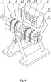
本発明の方法を行うにあたり、図3および図4に示す装置を用いるのが好ましい。詳細を以下に示す。
上記の方法および装置により、ガリウムまたはアルミニウム含有窒化物バルク単結晶を形成できる。バルク単結晶は低い欠陥密度を示す(バルクGaNの場合:104/cm2)バルク単結晶GaNは内径が1インチ以上、同時に、3mm以上(好ましくは5mm)の厚さを有することが重要である。単結晶をワイヤーソーでウエハに切断し、0.5mm厚のバルク単結晶基板を得る。バルク単結晶基板を後にシードとして用いることができる。n型導電性を改良するためには、気相成長中にSiをドープすることによりn型キャリア濃度を増加させるのが好ましい。ガリウムまたはアルミニウム含有窒化物を気相成長を用いて積層すれば、超臨界アンモニア中で形成するガリウムまたはアルミニウム含有窒化物がAlxGa1−xN(0≦x<1)を有するか、GaN上に積層したバルク単結晶AlxGa1−xN(0≦x<1)を用いるのが好ましい。ガリウムまたはアルミニウム含有窒化物の気相成長中にSiをドープすることにより、n型導電性を有するAlxGa1−x−yInyN、(0≦x≦1、0≦y<1、0≦x+y≦1)を形成でき、それを超臨界アンモニア中で、気相成長条件下でガリウムまたはアルミニウム含有窒化物上に結晶化させるので、高い結晶性及び105/cm2以下の欠陥密度を有するテンプレート型基板の形成に使用することができる。
本発明の方法においては、フィードストックの溶解工程と、超臨界溶液をより高温および/またはより低圧に輸送する工程とを分離でき、シードの表面にガリウムまたはアルミニウム含有窒化物の結晶化が生じる。さらに、該方法は、オートクレーブ中の異なる温度を有する少なくとも2つの領域を同時に形成する工程をそなえ、ガリウムまたはアルミニウム含有フィードストックをより低温の溶解領域に、シードをより高温の結晶化領域に配置する。溶解領域と結晶化領域間の温度差は1℃以上となるように制御し、超臨界溶液内での対流による化学輸送を確保する。超臨界アンモニア内で形成したガリウムまたはアルミニウム含有窒化物は、AlxGa1−xN、(0≦x<1)であり、ドナー型、アクセプター型、または磁気型の添加物を含有してもよく、一方、気相成長で形成したガリウムまたはアルミニウム含有窒化物は、AlxGa1−x−yInyN、(0≦x≦1、0≦y<1、0≦x+y≦1)である。
アルカリ金属イオンおよび/またはその誘導体を含んだアンモニアは超臨界溶媒として機能できる。フィードストックは主として、アジド類、イミド類、アミド−イミド類、アミド類、水素化物、金属間化合物およびガリウムまたはアルミニウム含有合金からなる群から選択されたガリウムまたはアルミニウム含有窒化物またはその前駆体と同様に、金属ガリウムからなる。シードは少なくともガリウムまたはアルミニウム含有窒化物または第XIII族(IUPAC, 1989)の他の元素の結晶層を備える。
半導体装置の適切な品質と寿命を確保できる。同時に、基板が導電性を有するので、n型パッド電極をその上に積層できる。
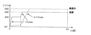
1)HVPE−GaNシード上に成長した5mmの単結晶の層を、加熱炉内に配置し、1〜5時間、600〜900℃、若干の酸素を含む窒素雰囲気で、アニール処理を行う。
2)次に、タカトリ(株)のワイヤーソーにサンプルを設置する。設置する際にはサンプルに結晶の主軸に適したオフ角を形成するため、1°以下傾けて設置する。その後ワイヤーソーを用いて5枚のウエハに切断し、0.05〜0.2度のオフ角のサンプルを得る。
3)次にサンプルを加熱炉内に設置し、1〜5時間、600〜900℃、若干の酸素を含む窒素雰囲気で、再度アニール処理を行う(以下、これをGaN基板と呼ぶ)。
4)次に、作業台上にGaN基板を載せ、ロジッテック社の研磨機にかけて、片面ずつ研磨する。研磨の行程においてはダイヤモンドツール及びシリカまたはアルミナスラリー溶液(pH3〜6またはpH9〜11)を用い、最終面10オングストローム以下の粗さに仕上げる。
5)その後、HVPE法またはMOCVD法にてGaN基板表面に(1〜数μm厚の)GaNまたはAlGaNの保護層を加え、テンプレート型基板を得る。
6)あるいは、上記保護層を備えるGaN基板上、または同保護層を備えないGaN基板上のいずれかに、3mm厚のGaN層を以下に示す一定条件の下でHVPE法により形成する。上記種々の方法を用いて切断、研磨した後、0.5mm厚のテンプレート型基板が形成され、オプトエレクトロニクス機器に使用される。HVPE条件は以下の通りである:反応温度:1050℃、反応圧力:気圧(0.1Mpa)、アンモニア分圧0.03Mpa、GaCl3分圧:100Pa、水素キャリアガス。
7)GaNまたはAlGaNにかわり、SiCまたはZnOからなる別の保護層をGaN基板上に形成でき、さらに3mm厚のGaN層をHVPE法を用いて形成できる。
Claims (14)
- オプトエレクトロニクスまたはエレクトロニクス機器のための基板の製造方法であって、
(a)超臨界アンモニア含有溶液からシード上にガリウムまたはアルミニウム含有窒化物を結晶させて、アルカリ金属(I族元素、IUPAC1989)の少なくとも1種を含有する窒化物バルク単結晶の層A)を、基板のための膜厚をもたせて形成する工程と、
(b)気相エピタキシャル成長法により、層A)のAlまたはGa極性面上に窒化物の層を100μm以上の厚さに形成する工程と、
(c)層A)から、工程(b)において形成した窒化物の層を100μm 以上の厚さに切り出し、主面が実質的にAl極性面またはGa極性面を有する基板を形成する工程と、を備えることを特徴とする製造方法。 - 前記工程(b)において、(b1)窒化物の第1層をMOCVD法またはMBE法により、層A)のAlまたはGa極性面上に形成し、(b2)窒化物の第2層をHVPE法により、100μm 以上の厚さに前記第1層上に形成することにより前記窒化物の層を形成し、
前記工程(c)において、 層A)から前記第2層を切り出すことを特徴とする請求項1記載の製造方法。 - 前記第1層がMOCVD法により形成され、膜厚が0.1から3μmであることを特徴とする請求項2記載の製造方法。
- 前記第2層の1つの表面を研磨し、気相エピタキシャル成長用の基板を得る工程をさらに備えることを特徴とする請求項3に記載の製造方法。
- 水素を含有しない空気中で、600℃ から1050℃ の温度で、工程(b)において形成した窒化物の層または第2層をアニーリング処理し、アニーリング処理前よりもより良好な結晶性を有する材料を製造する工程をさらに備えることを特徴とする請求項1から4のいずれかに記載の製造方法。
- 前記アニーリング処理を10から30Vol.%の酸素を添加した不活性ガスの空気中で行うことを特徴とする請求項5に記載の製造方法。
- 不純物(水素および/またはアンモニアまたは結晶および/またはアニーリング処理中に生じた不純物から形成されたイオン)が望ましいレベルに達するまで、アニーリング処理を単一工程または複数の工程で行うことを特徴とする請求項5に記載の製造方法。
- アンモニア含有溶媒、水または二酸化炭素の超臨界環境下に浸漬、またはガス状水素、窒素またはアンモニアの作用下に付し、窒化物バルク単結晶から不純物を除去する工程をさらに備えることを特徴とする請求項1から7のいずれかに記載の製造方法。
- 洗浄工程で超音波または電子ビーム照射を補助的に用いることを特徴とする請求項8に記載の製造方法。
- 前記(a)工程において、層A)はA軸成長されてC面からなる上面を有する請求項1から9のいずれかに記載の製造方法。
- 前記(c)工程で、切り出される基板の直径が1インチ以上である請求項1〜10のいずれかに記載の製造方法。
- 前記窒化物の層がAlxGa1−xN(0≦x≦1)で表わされる窒化物からなる請求項1から11のいずれかに記載の製造方法。
- 前記第2層がAlxGa1−xN(0≦x≦1)で表わされる窒化物からなる請求項1から12のいずれかに記載の製造方法。
- 前記(c)工程で、切り出される基板の厚さが150μm以上である請求項1から13いずれかに記載の製造方法。
Applications Claiming Priority (9)
| Application Number | Priority Date | Filing Date | Title |
|---|---|---|---|
| PL02357708A PL357708A1 (en) | 2002-12-11 | 2002-12-11 | Method of fabrication of epitaxial layer standardized substrate (template type substrates) from voluminal mono-crystalline aluminium nitride and nitride containing gallium for epitaxy of layers with high aluminium content as well as devices requiring efficient heat abstraction |
| PLP-357696 | 2002-12-11 | ||
| PLP-357707 | 2002-12-11 | ||
| PL357696A PL225423B1 (pl) | 2002-12-11 | 2002-12-11 | Sposób wytwarzania podłoża standaryzowanego warstwą epitaksjalną ( podłoża typu template), z objętościowego monokrystalicznego azotku zawierającego gal |
| PLP-357709 | 2002-12-11 | ||
| PLP-357708 | 2002-12-11 | ||
| PL357709A PL225425B1 (pl) | 2002-12-11 | 2002-12-11 | Sposób wytwarzania złożonego podłoża standaryzowanego warstwą epitaksjalną (podłoża typu template) z objętościowego monokrystalicznego azotku zawierającego gal |
| PL357707A PL225424B1 (pl) | 2002-12-11 | 2002-12-11 | Sposób wytwarzania podłoża typu template z objętościowego monokrystalicznego azotku zawierającego gal |
| PCT/JP2003/015906 WO2004053210A1 (en) | 2002-12-11 | 2003-12-11 | A substrate for epitaxy and a method of preparing the same |
Publications (3)
| Publication Number | Publication Date |
|---|---|
| JP2006509710A JP2006509710A (ja) | 2006-03-23 |
| JP2006509710A5 JP2006509710A5 (ja) | 2007-02-01 |
| JP4860927B2 true JP4860927B2 (ja) | 2012-01-25 |
Family
ID=32512483
Family Applications (2)
| Application Number | Title | Priority Date | Filing Date |
|---|---|---|---|
| JP2004558482A Expired - Fee Related JP4558502B2 (ja) | 2002-12-11 | 2003-12-11 | テンプレート型基板の製造方法 |
| JP2004558483A Expired - Lifetime JP4860927B2 (ja) | 2002-12-11 | 2003-12-11 | エピタキシ用基板及びその製造方法 |
Family Applications Before (1)
| Application Number | Title | Priority Date | Filing Date |
|---|---|---|---|
| JP2004558482A Expired - Fee Related JP4558502B2 (ja) | 2002-12-11 | 2003-12-11 | テンプレート型基板の製造方法 |
Country Status (11)
| Country | Link |
|---|---|
| US (3) | US7387677B2 (ja) |
| EP (2) | EP1576210B1 (ja) |
| JP (2) | JP4558502B2 (ja) |
| KR (2) | KR100789889B1 (ja) |
| AT (2) | ATE445722T1 (ja) |
| AU (2) | AU2003285768A1 (ja) |
| DE (2) | DE60331245D1 (ja) |
| HK (1) | HK1083030A1 (ja) |
| PL (2) | PL224992B1 (ja) |
| TW (2) | TWI334229B (ja) |
| WO (2) | WO2004053210A1 (ja) |
Families Citing this family (78)
| Publication number | Priority date | Publication date | Assignee | Title |
|---|---|---|---|---|
| TWI277666B (en) * | 2001-06-06 | 2007-04-01 | Ammono Sp Zoo | Process and apparatus for obtaining bulk mono-crystalline gallium-containing nitride |
| US7750355B2 (en) * | 2001-10-26 | 2010-07-06 | Ammono Sp. Z O.O. | Light emitting element structure using nitride bulk single crystal layer |
| US7638346B2 (en) * | 2001-12-24 | 2009-12-29 | Crystal Is, Inc. | Nitride semiconductor heterostructures and related methods |
| US8545629B2 (en) | 2001-12-24 | 2013-10-01 | Crystal Is, Inc. | Method and apparatus for producing large, single-crystals of aluminum nitride |
| US20060005763A1 (en) * | 2001-12-24 | 2006-01-12 | Crystal Is, Inc. | Method and apparatus for producing large, single-crystals of aluminum nitride |
| US20060138431A1 (en) | 2002-05-17 | 2006-06-29 | Robert Dwilinski | Light emitting device structure having nitride bulk single crystal layer |
| JP4416648B2 (ja) * | 2002-05-17 | 2010-02-17 | アンモノ・スプウカ・ジ・オグラニチョノン・オドポヴィエドニアウノシツィオン | 発光素子の製造方法 |
| US7811380B2 (en) * | 2002-12-11 | 2010-10-12 | Ammono Sp. Z O.O. | Process for obtaining bulk mono-crystalline gallium-containing nitride |
| AU2003285768A1 (en) | 2002-12-11 | 2004-06-30 | Ammono Sp. Z O.O. | A template type substrate and a method of preparing the same |
| US7351994B2 (en) * | 2004-01-21 | 2008-04-01 | Taiwan Semiconductor Manufacturing Company | Noble high-k device |
| KR100848380B1 (ko) | 2004-06-11 | 2008-07-25 | 암모노 에스피. 제트오. 오. | 갈륨 함유 질화물의 벌크 단결정 및 그의 어플리케이션 |
| PL371405A1 (pl) | 2004-11-26 | 2006-05-29 | Ammono Sp.Z O.O. | Sposób wytwarzania objętościowych monokryształów metodą wzrostu na zarodku |
| EP1864338A4 (en) * | 2005-02-04 | 2010-01-20 | Seoul Opto Device Co Ltd | LIGHT-EMITTING COMPONENT WITH SEVERAL LIGHT-EMITTING CELLS AND MANUFACTURING METHOD THEREFOR |
| JP4563230B2 (ja) | 2005-03-28 | 2010-10-13 | 昭和電工株式会社 | AlGaN基板の製造方法 |
| US20060288929A1 (en) * | 2005-06-10 | 2006-12-28 | Crystal Is, Inc. | Polar surface preparation of nitride substrates |
| JP4277826B2 (ja) * | 2005-06-23 | 2009-06-10 | 住友電気工業株式会社 | 窒化物結晶、窒化物結晶基板、エピ層付窒化物結晶基板、ならびに半導体デバイスおよびその製造方法 |
| WO2007006001A2 (en) | 2005-07-06 | 2007-01-11 | International Rectifier Corporation | Iii-nitride enhancement mode devices |
| US20070069225A1 (en) * | 2005-09-27 | 2007-03-29 | Lumileds Lighting U.S., Llc | III-V light emitting device |
| EP1775356A3 (en) * | 2005-10-14 | 2009-12-16 | Ricoh Company, Ltd. | Crystal growth apparatus and manufacturing method of group III nitride crystal |
| CN101415864B (zh) * | 2005-11-28 | 2014-01-08 | 晶体公司 | 具有减少缺陷的大的氮化铝晶体及其制造方法 |
| JP5281408B2 (ja) | 2005-12-02 | 2013-09-04 | クリスタル・イズ,インコーポレイテッド | ドープされた窒化アルミニウム結晶及びそれを製造する方法 |
| JP2009530798A (ja) | 2006-01-05 | 2009-08-27 | イルミテックス, インコーポレイテッド | Ledから光を導くための独立した光学デバイス |
| JP2007277074A (ja) * | 2006-01-10 | 2007-10-25 | Ngk Insulators Ltd | 窒化アルミニウム単結晶の製造方法及び窒化アルミニウム単結晶 |
| KR100714629B1 (ko) * | 2006-03-17 | 2007-05-07 | 삼성전기주식회사 | 질화물 반도체 단결정 기판, 그 제조방법 및 이를 이용한수직구조 질화물 발광소자 제조방법 |
| KR101155061B1 (ko) * | 2006-03-22 | 2012-06-11 | 삼성코닝정밀소재 주식회사 | 질화물 반도체 기판 및 이의 제조방법 |
| EP2918708B1 (en) * | 2006-03-30 | 2019-10-30 | Crystal Is, Inc. | Method for annealing of aluminium nitride wafer |
| US9034103B2 (en) * | 2006-03-30 | 2015-05-19 | Crystal Is, Inc. | Aluminum nitride bulk crystals having high transparency to ultraviolet light and methods of forming them |
| US20100095882A1 (en) * | 2008-10-16 | 2010-04-22 | Tadao Hashimoto | Reactor design for growing group iii nitride crystals and method of growing group iii nitride crystals |
| CN101437987A (zh) * | 2006-04-07 | 2009-05-20 | 加利福尼亚大学董事会 | 生长大表面积氮化镓晶体 |
| US8253221B2 (en) | 2007-09-19 | 2012-08-28 | The Regents Of The University Of California | Gallium nitride bulk crystals and their growth method |
| US7755172B2 (en) * | 2006-06-21 | 2010-07-13 | The Regents Of The University Of California | Opto-electronic and electronic devices using N-face or M-plane GaN substrate prepared with ammonothermal growth |
| US9803293B2 (en) * | 2008-02-25 | 2017-10-31 | Sixpoint Materials, Inc. | Method for producing group III-nitride wafers and group III-nitride wafers |
| US7789531B2 (en) | 2006-10-02 | 2010-09-07 | Illumitex, Inc. | LED system and method |
| EP2100990A1 (en) | 2006-10-16 | 2009-09-16 | Mitsubishi Chemical Corporation | Process for producing nitride semiconductor, crystal growth rate enhancement agent, nitride single crystal, wafer and device |
| JP2008160025A (ja) * | 2006-12-26 | 2008-07-10 | Sharp Corp | 窒化物半導体発光素子 |
| JP5125098B2 (ja) * | 2006-12-26 | 2013-01-23 | 信越半導体株式会社 | 窒化物半導体自立基板の製造方法 |
| US9771666B2 (en) | 2007-01-17 | 2017-09-26 | Crystal Is, Inc. | Defect reduction in seeded aluminum nitride crystal growth |
| US9028612B2 (en) | 2010-06-30 | 2015-05-12 | Crystal Is, Inc. | Growth of large aluminum nitride single crystals with thermal-gradient control |
| WO2008088838A1 (en) | 2007-01-17 | 2008-07-24 | Crystal Is, Inc. | Defect reduction in seeded aluminum nitride crystal growth |
| CN101652832B (zh) * | 2007-01-26 | 2011-06-22 | 晶体公司 | 厚的赝晶氮化物外延层 |
| US8080833B2 (en) | 2007-01-26 | 2011-12-20 | Crystal Is, Inc. | Thick pseudomorphic nitride epitaxial layers |
| US8269251B2 (en) | 2007-05-17 | 2012-09-18 | Mitsubishi Chemical Corporation | Method for producing group III nitride semiconductor crystal, group III nitride semiconductor substrate, and semiconductor light-emitting device |
| US8088220B2 (en) * | 2007-05-24 | 2012-01-03 | Crystal Is, Inc. | Deep-eutectic melt growth of nitride crystals |
| EP2240968A1 (en) | 2008-02-08 | 2010-10-20 | Illumitex, Inc. | System and method for emitter layer shaping |
| JP2011523931A (ja) * | 2008-05-28 | 2011-08-25 | ザ リージェンツ オブ ザ ユニバーシティ オブ カリフォルニア | 低濃度アルカリ金属保有の六方晶系ウルツ鉱型エピタキシャル層およびその生成方法 |
| EP2281076A1 (en) | 2008-06-04 | 2011-02-09 | Sixpoint Materials, Inc. | Methods for producing improved crystallinty group iii-nitride crystals from initial group iii-nitride seed by ammonothermal growth |
| TWI460323B (zh) | 2008-06-04 | 2014-11-11 | Sixpoint Materials Inc | 用於生長第iii族氮化物結晶之高壓容器及使用高壓容器生長第iii族氮化物結晶之方法及第iii族氮化物結晶 |
| EP2286007B1 (en) | 2008-06-12 | 2018-04-04 | SixPoint Materials, Inc. | Method for testing gallium nitride wafers and method for producing gallium nitride wafers |
| JP5177084B2 (ja) * | 2008-08-06 | 2013-04-03 | 住友電気工業株式会社 | 波長変換素子および波長変換素子の製造方法 |
| KR20110097813A (ko) * | 2008-11-07 | 2011-08-31 | 더 리전츠 오브 더 유니버시티 오브 캘리포니아 | Ⅲ족 질화물 결정들의 암모노열 성장을 위한 신규한 용기 설계 및 소스 물질과 씨드 결정들의 상기 용기에 대한 상대적인 배치 |
| US8852341B2 (en) * | 2008-11-24 | 2014-10-07 | Sixpoint Materials, Inc. | Methods for producing GaN nutrient for ammonothermal growth |
| JP4867981B2 (ja) * | 2008-12-04 | 2012-02-01 | 住友電気工業株式会社 | GaN結晶の成長方法 |
| TW201034256A (en) | 2008-12-11 | 2010-09-16 | Illumitex Inc | Systems and methods for packaging light-emitting diode devices |
| WO2010129718A2 (en) | 2009-05-05 | 2010-11-11 | Sixpoint Materials, Inc. | Growth reactor for gallium-nitride crystals using ammonia and hydrogen chloride |
| US20100314551A1 (en) * | 2009-06-11 | 2010-12-16 | Bettles Timothy J | In-line Fluid Treatment by UV Radiation |
| US8449128B2 (en) | 2009-08-20 | 2013-05-28 | Illumitex, Inc. | System and method for a lens and phosphor layer |
| US8585253B2 (en) | 2009-08-20 | 2013-11-19 | Illumitex, Inc. | System and method for color mixing lens array |
| JP5310534B2 (ja) | 2009-12-25 | 2013-10-09 | 豊田合成株式会社 | Iii族窒化物半導体の製造方法 |
| JPWO2011108640A1 (ja) * | 2010-03-04 | 2013-06-27 | Jx日鉱日石金属株式会社 | 結晶成長装置、窒化物系化合物半導体結晶の製造方法及び窒化物系化合物半導体結晶 |
| PL224995B1 (pl) | 2010-04-06 | 2017-02-28 | Inst Wysokich Ciśnień Polskiej Akademii Nauk | Podłoże do wzrostu epitaksjalnego |
| US9142412B2 (en) | 2011-02-03 | 2015-09-22 | Soitec | Semiconductor devices including substrate layers and overlying semiconductor layers having closely matching coefficients of thermal expansion, and related methods |
| US8436363B2 (en) | 2011-02-03 | 2013-05-07 | Soitec | Metallic carrier for layer transfer and methods for forming the same |
| US9082948B2 (en) | 2011-02-03 | 2015-07-14 | Soitec | Methods of fabricating semiconductor structures using thermal spray processes, and semiconductor structures fabricated using such methods |
| US8962359B2 (en) | 2011-07-19 | 2015-02-24 | Crystal Is, Inc. | Photon extraction from nitride ultraviolet light-emitting devices |
| US8960657B2 (en) | 2011-10-05 | 2015-02-24 | Sunedison, Inc. | Systems and methods for connecting an ingot to a wire saw |
| JP5888208B2 (ja) * | 2011-11-18 | 2016-03-16 | 三菱化学株式会社 | 窒化物結晶の製造方法 |
| CN103243389B (zh) | 2012-02-08 | 2016-06-08 | 丰田合成株式会社 | 制造第III族氮化物半导体单晶的方法及制造GaN衬底的方法 |
| JP5754391B2 (ja) * | 2012-02-08 | 2015-07-29 | 豊田合成株式会社 | Iii族窒化物半導体結晶の製造方法 |
| JP2014027092A (ja) * | 2012-07-26 | 2014-02-06 | Sharp Corp | 半導体発光素子 |
| JP6137197B2 (ja) | 2012-12-17 | 2017-05-31 | 三菱化学株式会社 | 窒化ガリウム基板、および、窒化物半導体結晶の製造方法 |
| JP6275817B2 (ja) | 2013-03-15 | 2018-02-07 | クリスタル アイエス, インコーポレーテッドCrystal Is, Inc. | 仮像電子及び光学電子装置に対する平面コンタクト |
| JP5999443B2 (ja) | 2013-06-07 | 2016-09-28 | 豊田合成株式会社 | III 族窒化物半導体結晶の製造方法およびGaN基板の製造方法 |
| JP6015566B2 (ja) | 2013-06-11 | 2016-10-26 | 豊田合成株式会社 | III 族窒化物半導体のエッチング方法およびIII 族窒化物半導体結晶の製造方法およびGaN基板の製造方法 |
| JP6516738B2 (ja) | 2013-07-11 | 2019-05-22 | シックスポイント マテリアルズ, インコーポレイテッド | Iii族窒化物半導体を用いた電子デバイスおよびその製造方法、および該電子デバイスを製作するためのエピタキシャル多層ウエハ |
| JP2015115343A (ja) * | 2013-12-09 | 2015-06-22 | シャープ株式会社 | 窒化物半導体素子の製造方法 |
| JP6264990B2 (ja) * | 2014-03-26 | 2018-01-24 | 日亜化学工業株式会社 | 窒化物半導体基板の製造方法 |
| CN108023001B (zh) * | 2017-11-30 | 2020-03-10 | 武汉大学 | 蚀刻阻挡层结构、含其的外延片及该外延片的制作方法 |
| US11087975B1 (en) * | 2018-07-02 | 2021-08-10 | United States Of America As Represented By The Secretary Of The Air Force | Method for fabrication of orientation-patterned templates on common substrates |
Citations (5)
| Publication number | Priority date | Publication date | Assignee | Title |
|---|---|---|---|---|
| WO1995004845A1 (en) * | 1993-08-10 | 1995-02-16 | Centrum Badan Wysokocisnieniowych | Crystalline multilayer structure and manufacturing method thereof |
| WO1997013891A1 (en) * | 1995-10-13 | 1997-04-17 | Centrum Badan Wysokocisnieniowych | METHOD OF MANUFACTURING EPITAXIAL LAYERS OF GaN OR Ga(A1,In)N ON SINGLE CRYSTAL GaN AND MIXED Ga(A1,In)N SUBSTRATES |
| FR2796657A1 (fr) * | 1999-07-20 | 2001-01-26 | Thomson Csf | Procede de synthese de materiaux massifs monocristallins en nitrures d'elements de la colonne iii du tableau de la classification periodique |
| JP2001185718A (ja) * | 1999-12-24 | 2001-07-06 | Hitachi Cable Ltd | 窒化ガリウム系化合物半導体を用いた高電子移動度トランジスタ用エピタキシャルウェハの製造方法 |
| JP2002029897A (ja) * | 2000-07-10 | 2002-01-29 | Sumitomo Electric Ind Ltd | 単結晶GaN基板の製造方法と単結晶GaN基板 |
Family Cites Families (131)
| Publication number | Priority date | Publication date | Assignee | Title |
|---|---|---|---|---|
| US3922703A (en) * | 1974-04-03 | 1975-11-25 | Rca Corp | Electroluminescent semiconductor device |
| FR2514566A1 (fr) * | 1982-02-02 | 1983-04-15 | Bagratishvili Givi | Dispositif emetteur de lumiere semi-conducteur a base de nitrure de gallium et procede de fabrication dudit dispositif |
| JPS6065798A (ja) | 1983-09-19 | 1985-04-15 | Toyota Central Res & Dev Lab Inc | 窒化ガリウム単結晶の成長方法 |
| CN1014535B (zh) | 1988-12-30 | 1991-10-30 | 中国科学院物理研究所 | 利用改进的矿化剂生长磷酸钛氧钾单晶的方法 |
| US5096860A (en) * | 1990-05-25 | 1992-03-17 | Alcan International Limited | Process for producing unagglomerated single crystals of aluminum nitride |
| KR920004181B1 (ko) * | 1990-09-13 | 1992-05-30 | 한국과학기술연구원 | 입방정질화붕소의 제조방법 |
| US5190738A (en) * | 1991-06-17 | 1993-03-02 | Alcan International Limited | Process for producing unagglomerated single crystals of aluminum nitride |
| US5306662A (en) * | 1991-11-08 | 1994-04-26 | Nichia Chemical Industries, Ltd. | Method of manufacturing P-type compound semiconductor |
| US5456204A (en) * | 1993-05-28 | 1995-10-10 | Alfa Quartz, C.A. | Filtering flow guide for hydrothermal crystal growth |
| GB9412849D0 (en) * | 1993-08-02 | 1994-08-17 | Marketing Store Ltd | Package |
| EP0717788B1 (en) * | 1993-09-17 | 1997-07-30 | Brent International Plc. | Pre-rinse for phosphating metal surfaces |
| US5679152A (en) * | 1994-01-27 | 1997-10-21 | Advanced Technology Materials, Inc. | Method of making a single crystals Ga*N article |
| DE69511995T2 (de) | 1994-04-08 | 2000-04-20 | Japan Energy Corp | Verfahren zum züchten von galliumnitridhalbleiterkristallen und vorrichtung |
| US5599520A (en) * | 1994-11-03 | 1997-02-04 | Garces; Juan M. | Synthesis of crystalline porous solids in ammonia |
| US5777350A (en) | 1994-12-02 | 1998-07-07 | Nichia Chemical Industries, Ltd. | Nitride semiconductor light-emitting device |
| US5679965A (en) * | 1995-03-29 | 1997-10-21 | North Carolina State University | Integrated heterostructures of Group III-V nitride semiconductor materials including epitaxial ohmic contact, non-nitride buffer layer and methods of fabricating same |
| US5670798A (en) * | 1995-03-29 | 1997-09-23 | North Carolina State University | Integrated heterostructures of Group III-V nitride semiconductor materials including epitaxial ohmic contact non-nitride buffer layer and methods of fabricating same |
| JP3728332B2 (ja) * | 1995-04-24 | 2005-12-21 | シャープ株式会社 | 化合物半導体発光素子 |
| WO1997008759A1 (fr) * | 1995-08-31 | 1997-03-06 | Kabushiki Kaisha Toshiba | Dispositif emetteur de lumiere bleue et son procede de fabrication |
| US6377596B1 (en) * | 1995-09-18 | 2002-04-23 | Hitachi, Ltd. | Semiconductor materials, methods for fabricating semiconductor materials, and semiconductor devices |
| JP3563869B2 (ja) * | 1996-03-25 | 2004-09-08 | トヨタ自動車株式会社 | エンジン出力制御装置 |
| CN1065289C (zh) | 1996-07-22 | 2001-05-02 | 中国科学院物理研究所 | 一种制备掺杂钒酸盐单晶的水热生长方法 |
| JP3179346B2 (ja) * | 1996-08-27 | 2001-06-25 | 松下電子工業株式会社 | 窒化ガリウム結晶の製造方法 |
| JPH1084161A (ja) * | 1996-09-06 | 1998-03-31 | Sumitomo Electric Ind Ltd | 半導体レーザ及びその製造方法 |
| US6031858A (en) * | 1996-09-09 | 2000-02-29 | Kabushiki Kaisha Toshiba | Semiconductor laser and method of fabricating same |
| US6542526B1 (en) * | 1996-10-30 | 2003-04-01 | Hitachi, Ltd. | Optical information processor and semiconductor light emitting device suitable for the same |
| JPH111399A (ja) * | 1996-12-05 | 1999-01-06 | Lg Electron Inc | 窒化ガリウム半導体単結晶基板の製造方法並びにその基板を用いた窒化ガリウムダイオード |
| EP1017113B1 (en) * | 1997-01-09 | 2012-08-22 | Nichia Corporation | Nitride semiconductor device |
| US6677619B1 (en) * | 1997-01-09 | 2004-01-13 | Nichia Chemical Industries, Ltd. | Nitride semiconductor device |
| US5868837A (en) * | 1997-01-17 | 1999-02-09 | Cornell Research Foundation, Inc. | Low temperature method of preparing GaN single crystals |
| PL184902B1 (pl) * | 1997-04-04 | 2003-01-31 | Centrum Badan Wysokocisnieniowych Pan | Sposób usuwania nierówności i obszarów silnie zdefektowanych z powierzchni kryształów i warstw epitaksjalnych GaN i Ga AL In N |
| JP3491492B2 (ja) * | 1997-04-09 | 2004-01-26 | 松下電器産業株式会社 | 窒化ガリウム結晶の製造方法 |
| EP0942459B1 (en) | 1997-04-11 | 2012-03-21 | Nichia Corporation | Method of growing nitride semiconductors |
| US5888389A (en) * | 1997-04-24 | 1999-03-30 | Hydroprocessing, L.L.C. | Apparatus for oxidizing undigested wastewater sludges |
| PL183687B1 (pl) * | 1997-06-06 | 2002-06-28 | Centrum Badan | Sposób wytwarzania półprzewodnikowych związków grupy A-B o przewodnictwie elektrycznym typu p i typu n |
| GB2333521B (en) | 1997-06-11 | 2000-04-26 | Hitachi Cable | Nitride crystal growth method |
| TW519551B (en) | 1997-06-11 | 2003-02-01 | Hitachi Cable | Methods of fabricating nitride crystals and nitride crystals obtained therefrom |
| US6270569B1 (en) * | 1997-06-11 | 2001-08-07 | Hitachi Cable Ltd. | Method of fabricating nitride crystal, mixture, liquid phase growth method, nitride crystal, nitride crystal powders, and vapor phase growth method |
| US6593589B1 (en) * | 1998-01-30 | 2003-07-15 | The University Of New Mexico | Semiconductor nitride structures |
| US6249534B1 (en) * | 1998-04-06 | 2001-06-19 | Matsushita Electronics Corporation | Nitride semiconductor laser device |
| TW428331B (en) * | 1998-05-28 | 2001-04-01 | Sumitomo Electric Industries | Gallium nitride single crystal substrate and method of producing the same |
| JPH11340576A (ja) | 1998-05-28 | 1999-12-10 | Sumitomo Electric Ind Ltd | 窒化ガリウム系半導体デバイス |
| JP4005701B2 (ja) * | 1998-06-24 | 2007-11-14 | シャープ株式会社 | 窒素化合物半導体膜の形成方法および窒素化合物半導体素子 |
| JP2000031533A (ja) | 1998-07-14 | 2000-01-28 | Toshiba Corp | 半導体発光素子 |
| TW413956B (en) * | 1998-07-28 | 2000-12-01 | Sumitomo Electric Industries | Fluorescent substrate LED |
| US6335546B1 (en) * | 1998-07-31 | 2002-01-01 | Sharp Kabushiki Kaisha | Nitride semiconductor structure, method for producing a nitride semiconductor structure, and light emitting device |
| JP2000091637A (ja) | 1998-09-07 | 2000-03-31 | Rohm Co Ltd | 半導体発光素子の製法 |
| US6423984B1 (en) * | 1998-09-10 | 2002-07-23 | Toyoda Gosei Co., Ltd. | Light-emitting semiconductor device using gallium nitride compound semiconductor |
| US6252261B1 (en) * | 1998-09-30 | 2001-06-26 | Nec Corporation | GaN crystal film, a group III element nitride semiconductor wafer and a manufacturing process therefor |
| JP3592553B2 (ja) * | 1998-10-15 | 2004-11-24 | 株式会社東芝 | 窒化ガリウム系半導体装置 |
| DE69941921D1 (de) * | 1998-11-06 | 2010-03-04 | Panasonic Corp | Halbleitervorrichtung |
| TW498102B (en) * | 1998-12-28 | 2002-08-11 | Futaba Denshi Kogyo Kk | A process for preparing GaN fluorescent substance |
| US6372041B1 (en) * | 1999-01-08 | 2002-04-16 | Gan Semiconductor Inc. | Method and apparatus for single crystal gallium nitride (GaN) bulk synthesis |
| US20020096674A1 (en) * | 1999-01-08 | 2002-07-25 | Cho Hak Dong | Nucleation layer growth and lift-up of process for GaN wafer |
| JP2000216494A (ja) | 1999-01-20 | 2000-08-04 | Sanyo Electric Co Ltd | 半導体発光素子およびその製造方法 |
| EP1024524A2 (en) | 1999-01-27 | 2000-08-02 | Matsushita Electric Industrial Co., Ltd. | Deposition of dielectric layers using supercritical CO2 |
| US6177057B1 (en) * | 1999-02-09 | 2001-01-23 | The United States Of America As Represented By The Secretary Of The Navy | Process for preparing bulk cubic gallium nitride |
| JP3399392B2 (ja) * | 1999-02-19 | 2003-04-21 | 株式会社村田製作所 | 半導体発光素子、およびその製造方法 |
| WO2000052796A1 (fr) | 1999-03-04 | 2000-09-08 | Nichia Corporation | Element de laser semiconducteur au nitrure |
| JP3957918B2 (ja) | 1999-05-17 | 2007-08-15 | 独立行政法人科学技術振興機構 | 窒化ガリウム単結晶の育成方法 |
| US6592663B1 (en) * | 1999-06-09 | 2003-07-15 | Ricoh Company Ltd. | Production of a GaN bulk crystal substrate and a semiconductor device formed on a GaN bulk crystal substrate |
| JP4329229B2 (ja) | 1999-06-30 | 2009-09-09 | 住友電気工業株式会社 | Iii−v族窒化物半導体の成長方法および気相成長装置 |
| US6475277B1 (en) * | 1999-06-30 | 2002-11-05 | Sumitomo Electric Industries, Ltd. | Group III-V nitride semiconductor growth method and vapor phase growth apparatus |
| JP3968920B2 (ja) * | 1999-08-10 | 2007-08-29 | 双葉電子工業株式会社 | 蛍光体 |
| JP4646359B2 (ja) | 1999-09-09 | 2011-03-09 | シャープ株式会社 | 窒化物半導体発光素子の製造方法 |
| JP2001085737A (ja) * | 1999-09-10 | 2001-03-30 | Sharp Corp | 窒化物半導体発光素子 |
| US6265322B1 (en) | 1999-09-21 | 2001-07-24 | Agere Systems Guardian Corp. | Selective growth process for group III-nitride-based semiconductors |
| JP4145437B2 (ja) | 1999-09-28 | 2008-09-03 | 住友電気工業株式会社 | 単結晶GaNの結晶成長方法及び単結晶GaN基板の製造方法と単結晶GaN基板 |
| CN1113988C (zh) | 1999-09-29 | 2003-07-09 | 中国科学院物理研究所 | 一种氮化镓单晶的热液生长方法 |
| US6398867B1 (en) | 1999-10-06 | 2002-06-04 | General Electric Company | Crystalline gallium nitride and method for forming crystalline gallium nitride |
| EP1104031B1 (en) * | 1999-11-15 | 2012-04-11 | Panasonic Corporation | Nitride semiconductor laser diode and method of fabricating the same |
| JP2001168385A (ja) | 1999-12-06 | 2001-06-22 | Toyoda Gosei Co Ltd | Iii族窒化物系化合物半導体素子及びiii族窒化物系化合物半導体発光素子 |
| US6653663B2 (en) * | 1999-12-06 | 2003-11-25 | Matsushita Electric Industrial Co., Ltd. | Nitride semiconductor device |
| US7315599B1 (en) * | 1999-12-29 | 2008-01-01 | Intel Corporation | Skew correction circuit |
| US6355497B1 (en) * | 2000-01-18 | 2002-03-12 | Xerox Corporation | Removable large area, low defect density films for led and laser diode growth |
| JP3335974B2 (ja) | 2000-01-24 | 2002-10-21 | 星和電機株式会社 | 窒化ガリウム系半導体発光素子及びその製造方法 |
| US20010015437A1 (en) * | 2000-01-25 | 2001-08-23 | Hirotatsu Ishii | GaN field-effect transistor, inverter device, and production processes therefor |
| JP4429459B2 (ja) | 2000-03-03 | 2010-03-10 | 古河電気工業株式会社 | 高抵抗GaN結晶層の製造方法 |
| US6596079B1 (en) | 2000-03-13 | 2003-07-22 | Advanced Technology Materials, Inc. | III-V nitride substrate boule and method of making and using the same |
| US6447604B1 (en) * | 2000-03-13 | 2002-09-10 | Advanced Technology Materials, Inc. | Method for achieving improved epitaxy quality (surface texture and defect density) on free-standing (aluminum, indium, gallium) nitride ((al,in,ga)n) substrates for opto-electronic and electronic devices |
| JP3946427B2 (ja) | 2000-03-29 | 2007-07-18 | 株式会社東芝 | エピタキシャル成長用基板の製造方法及びこのエピタキシャル成長用基板を用いた半導体装置の製造方法 |
| WO2001080311A1 (en) * | 2000-04-17 | 2001-10-25 | Virginia Commonwealth University | Defect reduction in gan and related materials |
| JP2001339121A (ja) * | 2000-05-29 | 2001-12-07 | Sharp Corp | 窒化物半導体発光素子とそれを含む光学装置 |
| GB2363518A (en) | 2000-06-17 | 2001-12-19 | Sharp Kk | A method of growing a nitride layer on a GaN substrate |
| US6693935B2 (en) * | 2000-06-20 | 2004-02-17 | Sony Corporation | Semiconductor laser |
| JP2002016285A (ja) * | 2000-06-27 | 2002-01-18 | National Institute Of Advanced Industrial & Technology | 半導体発光素子 |
| US6586762B2 (en) * | 2000-07-07 | 2003-07-01 | Nichia Corporation | Nitride semiconductor device with improved lifetime and high output power |
| EP1176120A1 (en) * | 2000-07-28 | 2002-01-30 | Japan Pionics Co., Ltd. | Process for purifying ammonia |
| JP4190711B2 (ja) | 2000-08-31 | 2008-12-03 | 株式会社リコー | Iii族窒化物結晶の結晶製造方法および結晶製造装置 |
| JP4154558B2 (ja) * | 2000-09-01 | 2008-09-24 | 日本電気株式会社 | 半導体装置 |
| WO2002021604A1 (fr) * | 2000-09-08 | 2002-03-14 | Sharp Kabushiki Kaisha | Dispositif emetteur de lumiere a semi-conducteurs au nitrure |
| JP4416297B2 (ja) * | 2000-09-08 | 2010-02-17 | シャープ株式会社 | 窒化物半導体発光素子、ならびにそれを使用した発光装置および光ピックアップ装置 |
| JP2002094189A (ja) * | 2000-09-14 | 2002-03-29 | Sharp Corp | 窒化物半導体レーザ素子およびそれを用いた光学装置 |
| JP2002134416A (ja) | 2000-10-19 | 2002-05-10 | Ricoh Co Ltd | p型3族窒化物の結晶成長方法および製造方法、並びに半導体素子 |
| US6936488B2 (en) | 2000-10-23 | 2005-08-30 | General Electric Company | Homoepitaxial gallium-nitride-based light emitting device and method for producing |
| US7053413B2 (en) * | 2000-10-23 | 2006-05-30 | General Electric Company | Homoepitaxial gallium-nitride-based light emitting device and method for producing |
| JP4063520B2 (ja) * | 2000-11-30 | 2008-03-19 | 日本碍子株式会社 | 半導体発光素子 |
| KR100831751B1 (ko) | 2000-11-30 | 2008-05-23 | 노쓰 캐롤라이나 스테이트 유니버시티 | M'n 물의 제조 방법 및 장치 |
| JP4003413B2 (ja) | 2000-12-11 | 2007-11-07 | 日亜化学工業株式会社 | 13族窒化物結晶の製造方法 |
| JP3785566B2 (ja) | 2001-03-19 | 2006-06-14 | 株式会社日鉱マテリアルズ | GaN系化合物半導体結晶の製造方法 |
| US6806508B2 (en) * | 2001-04-20 | 2004-10-19 | General Electic Company | Homoepitaxial gallium nitride based photodetector and method of producing |
| JP4633962B2 (ja) | 2001-05-18 | 2011-02-16 | 日亜化学工業株式会社 | 窒化物半導体基板の製造方法 |
| US6734530B2 (en) | 2001-06-06 | 2004-05-11 | Matsushita Electric Industries Co., Ltd. | GaN-based compound semiconductor EPI-wafer and semiconductor element using the same |
| TWI277666B (en) * | 2001-06-06 | 2007-04-01 | Ammono Sp Zoo | Process and apparatus for obtaining bulk mono-crystalline gallium-containing nitride |
| PL350375A1 (en) | 2001-10-26 | 2003-05-05 | Ammono Sp Z Oo | Epitaxial layer substrate |
| PL207400B1 (pl) * | 2001-06-06 | 2010-12-31 | Ammono Społka Z Ograniczoną Odpowiedzialnością | Sposób i urządzenie do otrzymywania objętościowego monokryształu azotku zawierającego gal |
| US6488767B1 (en) * | 2001-06-08 | 2002-12-03 | Advanced Technology Materials, Inc. | High surface quality GaN wafer and method of fabricating same |
| JP2002009392A (ja) | 2001-06-22 | 2002-01-11 | Matsushita Electric Ind Co Ltd | 半導体発光素子およびその製造方法 |
| US6562466B2 (en) | 2001-07-02 | 2003-05-13 | Essilor International Compagnie Generale D'optique | Process for transferring a coating onto a surface of a lens blank |
| US7750355B2 (en) | 2001-10-26 | 2010-07-06 | Ammono Sp. Z O.O. | Light emitting element structure using nitride bulk single crystal layer |
| CN1316070C (zh) * | 2001-10-26 | 2007-05-16 | 波兰商艾蒙诺公司 | 取向生长用基底 |
| US6949140B2 (en) | 2001-12-05 | 2005-09-27 | Ricoh Company, Ltd. | Crystal growth method, crystal growth apparatus, group-III nitride crystal and group-III nitride semiconductor device |
| US7097707B2 (en) * | 2001-12-31 | 2006-08-29 | Cree, Inc. | GaN boule grown from liquid melt using GaN seed wafers |
| US20030209191A1 (en) | 2002-05-13 | 2003-11-13 | Purdy Andrew P. | Ammonothermal process for bulk synthesis and growth of cubic GaN |
| TWI274735B (en) * | 2002-05-17 | 2007-03-01 | Ammono Sp Zoo | Bulk single crystal production facility employing supercritical ammonia |
| US20060138431A1 (en) | 2002-05-17 | 2006-06-29 | Robert Dwilinski | Light emitting device structure having nitride bulk single crystal layer |
| JP4416648B2 (ja) | 2002-05-17 | 2010-02-17 | アンモノ・スプウカ・ジ・オグラニチョノン・オドポヴィエドニアウノシツィオン | 発光素子の製造方法 |
| JP2005531154A (ja) | 2002-06-26 | 2005-10-13 | アンモノ・スプウカ・ジ・オグラニチョノン・オドポヴィエドニアウノシツィオン | 窒化物半導体レーザ素子及びその性能を向上させる方法 |
| EP1518009B1 (en) * | 2002-06-26 | 2013-07-17 | Ammono S.A. | Process for obtaining of bulk monocrystalline gallium-containing nitride |
| US7099073B2 (en) * | 2002-09-27 | 2006-08-29 | Lucent Technologies Inc. | Optical frequency-converters based on group III-nitrides |
| AU2003285768A1 (en) * | 2002-12-11 | 2004-06-30 | Ammono Sp. Z O.O. | A template type substrate and a method of preparing the same |
| US7811380B2 (en) | 2002-12-11 | 2010-10-12 | Ammono Sp. Z O.O. | Process for obtaining bulk mono-crystalline gallium-containing nitride |
| AU2003285766A1 (en) | 2002-12-11 | 2004-06-30 | Ammono Sp. Z O.O. | Process for obtaining bulk-crystalline gallium-containing nitride |
| KR100902525B1 (ko) | 2003-04-03 | 2009-06-15 | 미쓰비시 가가꾸 가부시키가이샤 | 산화아연 단결정 |
| KR100848380B1 (ko) | 2004-06-11 | 2008-07-25 | 암모노 에스피. 제트오. 오. | 갈륨 함유 질화물의 벌크 단결정 및 그의 어플리케이션 |
| US8754449B2 (en) | 2004-06-11 | 2014-06-17 | Ammono Sp. Z O.O. | High electron mobility transistor (HEMT) made of layers of Group XIII element nitrides and manufacturing method thereof |
| PL371405A1 (pl) | 2004-11-26 | 2006-05-29 | Ammono Sp.Z O.O. | Sposób wytwarzania objętościowych monokryształów metodą wzrostu na zarodku |
| US7704324B2 (en) | 2005-01-25 | 2010-04-27 | General Electric Company | Apparatus for processing materials in supercritical fluids and methods thereof |
| CN101437987A (zh) | 2006-04-07 | 2009-05-20 | 加利福尼亚大学董事会 | 生长大表面积氮化镓晶体 |
| US7803344B2 (en) | 2006-10-25 | 2010-09-28 | The Regents Of The University Of California | Method for growing group III-nitride crystals in a mixture of supercritical ammonia and nitrogen, and group III-nitride crystals grown thereby |
| US8253221B2 (en) | 2007-09-19 | 2012-08-28 | The Regents Of The University Of California | Gallium nitride bulk crystals and their growth method |
-
2003
- 2003-12-11 AU AU2003285768A patent/AU2003285768A1/en not_active Abandoned
- 2003-12-11 AT AT03778842T patent/ATE445722T1/de not_active IP Right Cessation
- 2003-12-11 WO PCT/JP2003/015906 patent/WO2004053210A1/en active Application Filing
- 2003-12-11 AT AT03778843T patent/ATE457372T1/de not_active IP Right Cessation
- 2003-12-11 TW TW092135277A patent/TWI334229B/zh active
- 2003-12-11 KR KR1020057010733A patent/KR100789889B1/ko active IP Right Grant
- 2003-12-11 JP JP2004558482A patent/JP4558502B2/ja not_active Expired - Fee Related
- 2003-12-11 TW TW092135267A patent/TWI352434B/zh active
- 2003-12-11 EP EP03778843A patent/EP1576210B1/en not_active Expired - Lifetime
- 2003-12-11 DE DE60331245T patent/DE60331245D1/de not_active Expired - Lifetime
- 2003-12-11 PL PL379546A patent/PL224992B1/pl unknown
- 2003-12-11 DE DE60329713T patent/DE60329713D1/de not_active Expired - Lifetime
- 2003-12-11 WO PCT/JP2003/015905 patent/WO2004053209A1/en active Application Filing
- 2003-12-11 JP JP2004558483A patent/JP4860927B2/ja not_active Expired - Lifetime
- 2003-12-11 EP EP03778842A patent/EP1581675B1/en not_active Expired - Lifetime
- 2003-12-11 US US10/538,407 patent/US7387677B2/en active Active
- 2003-12-11 PL PL379545A patent/PL224991B1/pl unknown
- 2003-12-11 AU AU2003285769A patent/AU2003285769A1/en not_active Abandoned
- 2003-12-11 US US10/538,654 patent/US7410539B2/en active Active
- 2003-12-11 KR KR1020057010670A patent/KR101060073B1/ko active IP Right Grant
-
2006
- 2006-02-20 HK HK06102217A patent/HK1083030A1/xx not_active IP Right Cessation
-
2008
- 2008-06-16 US US12/213,212 patent/US8110848B2/en active Active
Patent Citations (5)
| Publication number | Priority date | Publication date | Assignee | Title |
|---|---|---|---|---|
| WO1995004845A1 (en) * | 1993-08-10 | 1995-02-16 | Centrum Badan Wysokocisnieniowych | Crystalline multilayer structure and manufacturing method thereof |
| WO1997013891A1 (en) * | 1995-10-13 | 1997-04-17 | Centrum Badan Wysokocisnieniowych | METHOD OF MANUFACTURING EPITAXIAL LAYERS OF GaN OR Ga(A1,In)N ON SINGLE CRYSTAL GaN AND MIXED Ga(A1,In)N SUBSTRATES |
| FR2796657A1 (fr) * | 1999-07-20 | 2001-01-26 | Thomson Csf | Procede de synthese de materiaux massifs monocristallins en nitrures d'elements de la colonne iii du tableau de la classification periodique |
| JP2001185718A (ja) * | 1999-12-24 | 2001-07-06 | Hitachi Cable Ltd | 窒化ガリウム系化合物半導体を用いた高電子移動度トランジスタ用エピタキシャルウェハの製造方法 |
| JP2002029897A (ja) * | 2000-07-10 | 2002-01-29 | Sumitomo Electric Ind Ltd | 単結晶GaN基板の製造方法と単結晶GaN基板 |
Also Published As
Similar Documents
| Publication | Publication Date | Title |
|---|---|---|
| JP4860927B2 (ja) | エピタキシ用基板及びその製造方法 | |
| JP4663319B2 (ja) | ガリウム含有窒化物バルク単結晶の製造方法 | |
| KR101419940B1 (ko) | 알칼리 금속 이온을 이용한 초임계 암모니아에서의 질화물단결정 시드 성장 | |
| KR100848380B1 (ko) | 갈륨 함유 질화물의 벌크 단결정 및 그의 어플리케이션 | |
| JP4824313B2 (ja) | ガリウム含有窒化物バルク単結晶を得るためのプロセス、得られた結晶から不純物を排除するためのプロセス、及びガリウム含有窒化物バルク単結晶からなる基板を製造するためのプロセス | |
| RU2004116073A (ru) | Подложка для эпитаксии | |
| JP6137197B2 (ja) | 窒化ガリウム基板、および、窒化物半導体結晶の製造方法 | |
| JP2006509707A (ja) | ガリウム含有窒化物のバルク単結晶を得るための改良されたプロセス | |
| US10961619B2 (en) | Method for producing GaN crystal | |
| PL225423B1 (pl) | Sposób wytwarzania podłoża standaryzowanego warstwą epitaksjalną ( podłoża typu template), z objętościowego monokrystalicznego azotku zawierającego gal | |
| KR101094409B1 (ko) | 질화갈륨 단결정 후막의 제조 방법 | |
| PL221055B1 (pl) | Sposób wytwarzania objętościowego monokrystalicznego azotku zawierającego gal | |
| PL225424B1 (pl) | Sposób wytwarzania podłoża typu template z objętościowego monokrystalicznego azotku zawierającego gal | |
| PL225425B1 (pl) | Sposób wytwarzania złożonego podłoża standaryzowanego warstwą epitaksjalną (podłoża typu template) z objętościowego monokrystalicznego azotku zawierającego gal |
Legal Events
| Date | Code | Title | Description |
|---|---|---|---|
| A521 | Request for written amendment filed |
Free format text: JAPANESE INTERMEDIATE CODE: A523 Effective date: 20061211 |
|
| A621 | Written request for application examination |
Free format text: JAPANESE INTERMEDIATE CODE: A621 Effective date: 20061211 |
|
| RD03 | Notification of appointment of power of attorney |
Free format text: JAPANESE INTERMEDIATE CODE: A7423 Effective date: 20061211 |
|
| RD03 | Notification of appointment of power of attorney |
Free format text: JAPANESE INTERMEDIATE CODE: A7423 Effective date: 20090514 |
|
| A131 | Notification of reasons for refusal |
Free format text: JAPANESE INTERMEDIATE CODE: A131 Effective date: 20100330 |
|
| A601 | Written request for extension of time |
Free format text: JAPANESE INTERMEDIATE CODE: A601 Effective date: 20100625 |
|
| A602 | Written permission of extension of time |
Free format text: JAPANESE INTERMEDIATE CODE: A602 Effective date: 20100702 |
|
| A601 | Written request for extension of time |
Free format text: JAPANESE INTERMEDIATE CODE: A601 Effective date: 20100827 |
|
| A602 | Written permission of extension of time |
Free format text: JAPANESE INTERMEDIATE CODE: A602 Effective date: 20100903 |
|
| A521 | Request for written amendment filed |
Free format text: JAPANESE INTERMEDIATE CODE: A523 Effective date: 20100929 |
|
| A02 | Decision of refusal |
Free format text: JAPANESE INTERMEDIATE CODE: A02 Effective date: 20110301 |
|
| A521 | Request for written amendment filed |
Free format text: JAPANESE INTERMEDIATE CODE: A523 Effective date: 20110630 |
|
| A911 | Transfer to examiner for re-examination before appeal (zenchi) |
Free format text: JAPANESE INTERMEDIATE CODE: A911 Effective date: 20110812 |
|
| TRDD | Decision of grant or rejection written | ||
| A01 | Written decision to grant a patent or to grant a registration (utility model) |
Free format text: JAPANESE INTERMEDIATE CODE: A01 Effective date: 20111018 |
|
| A01 | Written decision to grant a patent or to grant a registration (utility model) |
Free format text: JAPANESE INTERMEDIATE CODE: A01 |
|
| A61 | First payment of annual fees (during grant procedure) |
Free format text: JAPANESE INTERMEDIATE CODE: A61 Effective date: 20111104 |
|
| R150 | Certificate of patent or registration of utility model |
Ref document number: 4860927 Country of ref document: JP Free format text: JAPANESE INTERMEDIATE CODE: R150 Free format text: JAPANESE INTERMEDIATE CODE: R150 |
|
| FPAY | Renewal fee payment (event date is renewal date of database) |
Free format text: PAYMENT UNTIL: 20141111 Year of fee payment: 3 |
|
| R250 | Receipt of annual fees |
Free format text: JAPANESE INTERMEDIATE CODE: R250 |
|
| R250 | Receipt of annual fees |
Free format text: JAPANESE INTERMEDIATE CODE: R250 |
|
| R250 | Receipt of annual fees |
Free format text: JAPANESE INTERMEDIATE CODE: R250 |
|
| R250 | Receipt of annual fees |
Free format text: JAPANESE INTERMEDIATE CODE: R250 |
|
| R250 | Receipt of annual fees |
Free format text: JAPANESE INTERMEDIATE CODE: R250 |
|
| R250 | Receipt of annual fees |
Free format text: JAPANESE INTERMEDIATE CODE: R250 |
|
| R250 | Receipt of annual fees |
Free format text: JAPANESE INTERMEDIATE CODE: R250 |
|
| R250 | Receipt of annual fees |
Free format text: JAPANESE INTERMEDIATE CODE: R250 |
|
| R250 | Receipt of annual fees |
Free format text: JAPANESE INTERMEDIATE CODE: R250 |